EP4325281A2 - Directional display apparatus - Google Patents
Directional display apparatus Download PDFInfo
- Publication number
- EP4325281A2 EP4325281A2 EP23218625.4A EP23218625A EP4325281A2 EP 4325281 A2 EP4325281 A2 EP 4325281A2 EP 23218625 A EP23218625 A EP 23218625A EP 4325281 A2 EP4325281 A2 EP 4325281A2
- Authority
- EP
- European Patent Office
- Prior art keywords
- pixels
- parallax barrier
- polariser
- retarder
- display device
- Prior art date
- Legal status (The legal status is an assumption and is not a legal conclusion. Google has not performed a legal analysis and makes no representation as to the accuracy of the status listed.)
- Pending
Links
Images


Classifications
-
- G—PHYSICS
- G02—OPTICS
- G02F—OPTICAL DEVICES OR ARRANGEMENTS FOR THE CONTROL OF LIGHT BY MODIFICATION OF THE OPTICAL PROPERTIES OF THE MEDIA OF THE ELEMENTS INVOLVED THEREIN; NON-LINEAR OPTICS; FREQUENCY-CHANGING OF LIGHT; OPTICAL LOGIC ELEMENTS; OPTICAL ANALOGUE/DIGITAL CONVERTERS
- G02F1/00—Devices or arrangements for the control of the intensity, colour, phase, polarisation or direction of light arriving from an independent light source, e.g. switching, gating or modulating; Non-linear optics
- G02F1/01—Devices or arrangements for the control of the intensity, colour, phase, polarisation or direction of light arriving from an independent light source, e.g. switching, gating or modulating; Non-linear optics for the control of the intensity, phase, polarisation or colour
- G02F1/13—Devices or arrangements for the control of the intensity, colour, phase, polarisation or direction of light arriving from an independent light source, e.g. switching, gating or modulating; Non-linear optics for the control of the intensity, phase, polarisation or colour based on liquid crystals, e.g. single liquid crystal display cells
- G02F1/133—Constructional arrangements; Operation of liquid crystal cells; Circuit arrangements
- G02F1/1333—Constructional arrangements; Manufacturing methods
- G02F1/1335—Structural association of cells with optical devices, e.g. polarisers or reflectors
- G02F1/133528—Polarisers
-
- H—ELECTRICITY
- H04—ELECTRIC COMMUNICATION TECHNIQUE
- H04N—PICTORIAL COMMUNICATION, e.g. TELEVISION
- H04N13/00—Stereoscopic video systems; Multi-view video systems; Details thereof
- H04N13/30—Image reproducers
- H04N13/302—Image reproducers for viewing without the aid of special glasses, i.e. using autostereoscopic displays
- H04N13/31—Image reproducers for viewing without the aid of special glasses, i.e. using autostereoscopic displays using parallax barriers
- H04N13/315—Image reproducers for viewing without the aid of special glasses, i.e. using autostereoscopic displays using parallax barriers the parallax barriers being time-variant
-
- H—ELECTRICITY
- H04—ELECTRIC COMMUNICATION TECHNIQUE
- H04N—PICTORIAL COMMUNICATION, e.g. TELEVISION
- H04N13/00—Stereoscopic video systems; Multi-view video systems; Details thereof
- H04N13/30—Image reproducers
- H04N13/302—Image reproducers for viewing without the aid of special glasses, i.e. using autostereoscopic displays
- H04N13/31—Image reproducers for viewing without the aid of special glasses, i.e. using autostereoscopic displays using parallax barriers
-
- G—PHYSICS
- G02—OPTICS
- G02B—OPTICAL ELEMENTS, SYSTEMS OR APPARATUS
- G02B30/00—Optical systems or apparatus for producing three-dimensional [3D] effects, e.g. stereoscopic images
- G02B30/20—Optical systems or apparatus for producing three-dimensional [3D] effects, e.g. stereoscopic images by providing first and second parallax images to an observer's left and right eyes
- G02B30/26—Optical systems or apparatus for producing three-dimensional [3D] effects, e.g. stereoscopic images by providing first and second parallax images to an observer's left and right eyes of the autostereoscopic type
- G02B30/30—Optical systems or apparatus for producing three-dimensional [3D] effects, e.g. stereoscopic images by providing first and second parallax images to an observer's left and right eyes of the autostereoscopic type involving parallax barriers
-
- G—PHYSICS
- G02—OPTICS
- G02F—OPTICAL DEVICES OR ARRANGEMENTS FOR THE CONTROL OF LIGHT BY MODIFICATION OF THE OPTICAL PROPERTIES OF THE MEDIA OF THE ELEMENTS INVOLVED THEREIN; NON-LINEAR OPTICS; FREQUENCY-CHANGING OF LIGHT; OPTICAL LOGIC ELEMENTS; OPTICAL ANALOGUE/DIGITAL CONVERTERS
- G02F1/00—Devices or arrangements for the control of the intensity, colour, phase, polarisation or direction of light arriving from an independent light source, e.g. switching, gating or modulating; Non-linear optics
- G02F1/01—Devices or arrangements for the control of the intensity, colour, phase, polarisation or direction of light arriving from an independent light source, e.g. switching, gating or modulating; Non-linear optics for the control of the intensity, phase, polarisation or colour
- G02F1/13—Devices or arrangements for the control of the intensity, colour, phase, polarisation or direction of light arriving from an independent light source, e.g. switching, gating or modulating; Non-linear optics for the control of the intensity, phase, polarisation or colour based on liquid crystals, e.g. single liquid crystal display cells
- G02F1/1323—Arrangements for providing a switchable viewing angle
-
- G—PHYSICS
- G02—OPTICS
- G02F—OPTICAL DEVICES OR ARRANGEMENTS FOR THE CONTROL OF LIGHT BY MODIFICATION OF THE OPTICAL PROPERTIES OF THE MEDIA OF THE ELEMENTS INVOLVED THEREIN; NON-LINEAR OPTICS; FREQUENCY-CHANGING OF LIGHT; OPTICAL LOGIC ELEMENTS; OPTICAL ANALOGUE/DIGITAL CONVERTERS
- G02F1/00—Devices or arrangements for the control of the intensity, colour, phase, polarisation or direction of light arriving from an independent light source, e.g. switching, gating or modulating; Non-linear optics
- G02F1/01—Devices or arrangements for the control of the intensity, colour, phase, polarisation or direction of light arriving from an independent light source, e.g. switching, gating or modulating; Non-linear optics for the control of the intensity, phase, polarisation or colour
- G02F1/13—Devices or arrangements for the control of the intensity, colour, phase, polarisation or direction of light arriving from an independent light source, e.g. switching, gating or modulating; Non-linear optics for the control of the intensity, phase, polarisation or colour based on liquid crystals, e.g. single liquid crystal display cells
- G02F1/133—Constructional arrangements; Operation of liquid crystal cells; Circuit arrangements
- G02F1/1333—Constructional arrangements; Manufacturing methods
- G02F1/13338—Input devices, e.g. touch panels
-
- G—PHYSICS
- G02—OPTICS
- G02F—OPTICAL DEVICES OR ARRANGEMENTS FOR THE CONTROL OF LIGHT BY MODIFICATION OF THE OPTICAL PROPERTIES OF THE MEDIA OF THE ELEMENTS INVOLVED THEREIN; NON-LINEAR OPTICS; FREQUENCY-CHANGING OF LIGHT; OPTICAL LOGIC ELEMENTS; OPTICAL ANALOGUE/DIGITAL CONVERTERS
- G02F1/00—Devices or arrangements for the control of the intensity, colour, phase, polarisation or direction of light arriving from an independent light source, e.g. switching, gating or modulating; Non-linear optics
- G02F1/01—Devices or arrangements for the control of the intensity, colour, phase, polarisation or direction of light arriving from an independent light source, e.g. switching, gating or modulating; Non-linear optics for the control of the intensity, phase, polarisation or colour
- G02F1/13—Devices or arrangements for the control of the intensity, colour, phase, polarisation or direction of light arriving from an independent light source, e.g. switching, gating or modulating; Non-linear optics for the control of the intensity, phase, polarisation or colour based on liquid crystals, e.g. single liquid crystal display cells
- G02F1/133—Constructional arrangements; Operation of liquid crystal cells; Circuit arrangements
- G02F1/1333—Constructional arrangements; Manufacturing methods
- G02F1/1335—Structural association of cells with optical devices, e.g. polarisers or reflectors
- G02F1/133553—Reflecting elements
-
- H—ELECTRICITY
- H10—SEMICONDUCTOR DEVICES; ELECTRIC SOLID-STATE DEVICES NOT OTHERWISE PROVIDED FOR
- H10K—ORGANIC ELECTRIC SOLID-STATE DEVICES
- H10K50/00—Organic light-emitting devices
- H10K50/80—Constructional details
- H10K50/86—Arrangements for improving contrast, e.g. preventing reflection of ambient light
- H10K50/865—Arrangements for improving contrast, e.g. preventing reflection of ambient light comprising light absorbing layers, e.g. light-blocking layers
-
- H—ELECTRICITY
- H10—SEMICONDUCTOR DEVICES; ELECTRIC SOLID-STATE DEVICES NOT OTHERWISE PROVIDED FOR
- H10K—ORGANIC ELECTRIC SOLID-STATE DEVICES
- H10K59/00—Integrated devices, or assemblies of multiple devices, comprising at least one organic light-emitting element covered by group H10K50/00
- H10K59/40—OLEDs integrated with touch screens
-
- H—ELECTRICITY
- H10—SEMICONDUCTOR DEVICES; ELECTRIC SOLID-STATE DEVICES NOT OTHERWISE PROVIDED FOR
- H10K—ORGANIC ELECTRIC SOLID-STATE DEVICES
- H10K59/00—Integrated devices, or assemblies of multiple devices, comprising at least one organic light-emitting element covered by group H10K50/00
- H10K59/50—OLEDs integrated with light modulating elements, e.g. with electrochromic elements, photochromic elements or liquid crystal elements
-
- H—ELECTRICITY
- H10—SEMICONDUCTOR DEVICES; ELECTRIC SOLID-STATE DEVICES NOT OTHERWISE PROVIDED FOR
- H10K—ORGANIC ELECTRIC SOLID-STATE DEVICES
- H10K59/00—Integrated devices, or assemblies of multiple devices, comprising at least one organic light-emitting element covered by group H10K50/00
- H10K59/80—Constructional details
- H10K59/8791—Arrangements for improving contrast, e.g. preventing reflection of ambient light
- H10K59/8792—Arrangements for improving contrast, e.g. preventing reflection of ambient light comprising light absorbing layers, e.g. black layers
-
- H—ELECTRICITY
- H10—SEMICONDUCTOR DEVICES; ELECTRIC SOLID-STATE DEVICES NOT OTHERWISE PROVIDED FOR
- H10K—ORGANIC ELECTRIC SOLID-STATE DEVICES
- H10K71/00—Manufacture or treatment specially adapted for the organic devices covered by this subclass
-
- G—PHYSICS
- G02—OPTICS
- G02B—OPTICAL ELEMENTS, SYSTEMS OR APPARATUS
- G02B2207/00—Coding scheme for general features or characteristics of optical elements and systems of subclass G02B, but not including elements and systems which would be classified in G02B6/00 and subgroups
- G02B2207/123—Optical louvre elements, e.g. for directional light blocking
-
- G—PHYSICS
- G02—OPTICS
- G02F—OPTICAL DEVICES OR ARRANGEMENTS FOR THE CONTROL OF LIGHT BY MODIFICATION OF THE OPTICAL PROPERTIES OF THE MEDIA OF THE ELEMENTS INVOLVED THEREIN; NON-LINEAR OPTICS; FREQUENCY-CHANGING OF LIGHT; OPTICAL LOGIC ELEMENTS; OPTICAL ANALOGUE/DIGITAL CONVERTERS
- G02F1/00—Devices or arrangements for the control of the intensity, colour, phase, polarisation or direction of light arriving from an independent light source, e.g. switching, gating or modulating; Non-linear optics
- G02F1/01—Devices or arrangements for the control of the intensity, colour, phase, polarisation or direction of light arriving from an independent light source, e.g. switching, gating or modulating; Non-linear optics for the control of the intensity, phase, polarisation or colour
- G02F1/13—Devices or arrangements for the control of the intensity, colour, phase, polarisation or direction of light arriving from an independent light source, e.g. switching, gating or modulating; Non-linear optics for the control of the intensity, phase, polarisation or colour based on liquid crystals, e.g. single liquid crystal display cells
- G02F1/133—Constructional arrangements; Operation of liquid crystal cells; Circuit arrangements
- G02F1/1333—Constructional arrangements; Manufacturing methods
- G02F1/1335—Structural association of cells with optical devices, e.g. polarisers or reflectors
- G02F1/133528—Polarisers
- G02F1/133531—Polarisers characterised by the arrangement of polariser or analyser axes
Definitions
- This disclosure generally relates to illumination from light modulation devices, and more specifically relates to optical stacks for providing control of illumination for use in display including privacy display and night-time display.
- Privacy displays provide image visibility to a primary user that is typically in an on-axis position and reduced visibility of image content to a snooper, that is typically in an off-axis position.
- a privacy function may be provided by micro-louvre optical films that transmit some light from a display in an on-axis direction with low luminance in off-axis positions.
- Such films have high losses for head-on illumination and the micro-louvres may cause Moiré artefacts due to beating with the pixels of the spatial light modulator.
- the pitch of the micro-louvre may need selection for panel resolution, increasing inventory and cost.
- Switchable privacy displays may be provided by control of the off-axis optical output.
- Control may be provided by means of luminance reduction, for example by means of switchable backlights for a liquid crystal display (LCD) spatial light modulator.
- Display backlights in general employ waveguides and edge emitting sources.
- Certain imaging directional backlights have the additional capability of directing the illumination through a display panel into viewing windows.
- An imaging system may be formed between multiple sources and the respective window images.
- One example of an imaging directional backlight is an optical valve that may employ a folded optical system and hence may also be an example of a folded imaging directional backlight.
- Light may propagate substantially without loss in one direction through the optical valve while counter-propagating light may be extracted by reflection off tilted facets as described in U.S. Patent No. 9,519,153 , which is herein incorporated by reference in its entirety.
- a display device comprising: an emissive spatial light modulator comprising an array of pixels arranged in a pixel layer; a parallax barrier forming an array of apertures, wherein the parallax barrier is separated from the pixel layer by a parallax distance along an axis along a normal to the plane of the pixel layer; each pixel being aligned with an aperture.
- the parallax barrier may direct light from each pixel into a common viewing window.
- a full resolution image with low reflectivity and reduced off-axis luminance may be achieved.
- the apertures Along the direction in which the apertures are closest, the apertures have a width a and the pixels have a width w that may meet the requirement that a ⁇ w.
- Advantageously full luminance may be achieved in at least one viewing direction.
- the apertures have a width a
- the pixels have a pitch p
- the pixels have a width w that may meet the requirement that a ⁇ (p-w/2).
- the off-axis luminance may be reduced to at most 50% for at least one viewing direction.
- the parallax barrier has a separation d from the pixels and the pixels have a pitch p along the direction in which the apertures are closest and material between the parallax barrier and the pixels has a refractive index n that may meet the requirement that 2 d / p ⁇ ⁇ 2 n 2 ⁇ 1 .
- the direction of minimum luminance may be at least 45 degrees to advantageously achieve desirable off-axis luminance for a privacy display.
- the parallax barrier has a separation d from the pixels and the apertures have a width a along the direction in which the apertures are closest and material between the parallax barrier and the pixels has a refractive index n that may meet the requirement that d ⁇ a ⁇ n 2 ⁇ 1 / 2 . At most 50% luminance is provided at a polar angle of 90 degrees to advantageously achieve desirable off-axis luminance for a privacy display.
- the parallax barrier has a separation d from the pixels and the apertures have a width a along the direction in which the apertures are closest and material between the parallax barrier and the pixels has a refractive index n that may meet the requirement that d ⁇ an ⁇ 1 ⁇ 3 / 4 n 2 / ⁇ 3 .
- At most 50% luminance is provided at a polar angle of 60 degrees to advantageously achieve desirable off-axis luminance for a privacy display.
- the pitch p' along the direction in which the apertures are closest may be smaller than the pitch p of the respective aligned pixels along the direction in which the pixels are closest; and the viewing window may be formed at a viewing window plane that is on the output side of the spatial light modulator.
- Advantageously luminance uniformity is increased for a head-on display user.
- the parallax barrier may form a two dimensional array of apertures, each pixel being aligned with a respective aperture. Luminance reduction may be achieved for lateral and elevation angles.
- a privacy display may be provided with landscape and portrait privacy operation. Display reflectivity may be reduced and display efficiency in a head-on direction increased.
- the pixels may be arranged in columns and rows, the direction in which the apertures are closest may be at 45 degrees with respect to the electric vector transmission direction of the output linear polariser; and each pixel may have a light emission region that is a square shape with edges rotated by 45 degrees with respect to the electric vector transmission direction of the output linear polariser.
- the apertures may have a square shape with edges rotated by 45 degrees with respect to the electric vector transmission direction of the output linear polariser; or the apertures may have a circular shape.
- Advantageously uniform luminance roll-off and reduced luminance at high polar angles may be achieved along lateral and elevation azimuthal directions.
- the light emission region may comprise light emitting sub-regions and non-light emitting sub-regions.
- the ratio of the area of light emitting sub-regions to non-light emitting regions may be different for red, green and blue pixels.
- the colour pixels may be driven with similar drive voltages to achieve matched output luminance to those that are provided in displays for which the parallax barrier is not provided.
- Advantageously control and driver electronics have reduced complexity and increased efficiency.
- the parallax barrier may form a one dimensional array of apertures, the pixels being arranged in columns, each column of pixels being aligned with a respective aperture. Modifications to pixel arrangements may be reduced, reducing cost.
- Each pixel may have a light emission region that is extended in the direction in which the apertures are extended; the width of the red, green and blue light emission regions may be the same for each of the pixels; and the height of the light emission regions may be different for red, green and blue light emitting pixels.
- the display may conveniently be rotated about an axis one direction to advantageously provide a comfortable viewing height for a head-on observer. The yield and cost of alignment of the parallax barrier may be reduced.
- the parallax barrier may be arranged to absorb light incident thereon. Display reflections may be reduced, advantageously increasing display contrast in brightly lit environments.
- the absorption of the region of the parallax barrier between the apertures may be less than 100%, and may be greater than 80% preferably greater than 90% and more preferably greater than 95%.
- the off-axis image visibility of the display may be increased in comparison to parallax barriers that are provided with 100% absorption in absorbing regions.
- the display device may be for use in ambient illumination and the parallax barrier may absorb at least some of the ambient illumination transmitted through the apertures that is reflected from the pixel layer. Reflections are reduced, advantageously increasing observed image contrast.
- the display device may have one or more additional layers between the pixel layer and the parallax barrier, wherein the pixels, the one or more additional layers and the parallax barrier may be formed as a monolithic stack.
- the separation of the pixel layer and parallax barrier layer may be provided with high stability during applied mechanical forces.
- the one or more additional layers may comprise at least one light transmitting inorganic layer arranged to provide a barrier to water and oxygen.
- the parallax barrier may comprise at least one light transmitting inorganic material that is arranged to provide a barrier to water and oxygen.
- the parallax barrier may be arranged between the pixel layer and at least one light transmitting inorganic layer that may be arranged to provide a barrier to water and oxygen.
- the lifetime of the display may be increased.
- An output polariser may be arranged on the output of the spatial light modulator, the output polariser being a linear polariser; and a reflection control quarter-wave retarder may be arranged between the output polariser and spatial light modulator.
- Advantageously reflections from the pixel layer may be reduced.
- the parallax barrier may be arranged between the pixel layer and the reflection control quarter-wave retarder.
- a small separation between the pixel layer and the parallax barrier may be conveniently achieved.
- the display device may further comprise an additional polariser arranged on the output side of the output polariser, the additional polariser being a linear polariser; and at least one polar control retarder arranged between the output polariser and the additional polariser.
- a privacy display may be provided that advantageously has high visual security level.
- At least one of the output polariser and additional polariser, when crossed with a notional polariser of the same material may have transmission for wavelengths from 520nm to 560nm that is less than the transmission for wavelengths from 450nm to 490nm.
- the transmission for wavelengths from 450nm to 490nm may be greater than 1%, preferably greater than 2% and most preferably greater than 3%; and the transmission for wavelengths from 520nm to 560nm may be less than 3%, preferably less than 2% and most preferably less than 1%.
- the transmission of the display may be increased in comparison to broadband absorbing polarisers.
- Advantageously display efficiency is increased.
- the transmission may be relatively greater for blue wavelengths.
- the lifetime of the display may be increased.
- the at least one polar control retarder may further comprise at least one passive retarder.
- the at least one polar control retarder may be capable of simultaneously introducing no net relative phase shift to orthogonal polarisation components of light passed by the output polariser along an axis along a normal to the plane of the at least one polar control retarder and introducing a relative phase shift to orthogonal polarisation components of light passed by the reflective polariser along an axis inclined to a normal to the plane of the at least one polar control retarder.
- the at least one passive retarder may comprise a retarder having its optical axis perpendicular to the plane of the retarder, the at least one passive retarder having a retardance for light of a wavelength of 550nm in a range from -150nm to -900nm, preferably in a range from -200nm to -500nm and most preferably in a range from -250nm to - 400nm.
- a large off-axis polar region with reduced luminance may be achieved.
- the visual security level is high for many snooper locations.
- the at least one retarder may comprise first and second quarter-wave plates arranged between the additional polariser and the output polariser, the first quarter-wave plate being arranged on the input side of the second quarter-wave plate and being arranged to convert a linearly polarised polarisation state passed by the output polariser on the input side thereof into a circularly polarised polarisation state, and the second quarter-wave plate on the output side being arranged to convert a circularly polarised polarisation state that is incident thereon into a linearly polarised polarisation state that is passed by the additional polariser on the output side thereof; and at least one retarder arranged between the pair of quarter-wave plates.
- the retarder arranged between the pair of quarter-wave plates may comprise a retarder having its optical axis perpendicular to the plane of the retarder, the at least one passive retarder having a retardance for light of a wavelength of 550nm in a range from -150nm to -500nm, preferably in a range from -200nm to -400nm and most preferably in a range from -250nm to -350nm.
- a rotationally symmetric polar luminance reduction profile may be provided.
- a privacy display may be operated in landscape and portrait modes. High visual security may be achieved for a snooper looking down from over a user's head.
- the at least one polar control retarder may comprise a switchable liquid crystal (LC) retarder comprising a layer of liquid crystal material and electrodes arranged to apply a voltage for switching the layer of liquid crystal material.
- the at least one polar control retarder may be arranged, in a first switchable state of the switchable liquid crystal retarder, simultaneously to introduce no net relative phase shift to orthogonal polarisation components of light passed by the reflective polariser along an axis along a normal to the plane of the at least one polar control retarder and to introduce a net relative phase shift to orthogonal polarisation components of light passed by the reflective polariser along an axis inclined to a normal to the plane of the at least one polar control retarder; and in a second switchable state of the switchable liquid crystal retarder, simultaneously to introduce no net relative phase shift to orthogonal polarisation components of light passed by the reflective polariser along an axis along a normal to the plane of the at least one polar control retarder and to introduce no net relative phase shift to orthogon
- a display may be switched between privacy and public modes of operation.
- the region for which high visual security is provided to an off-axis snooper in privacy mode and high image visibility is provided to an off-axis user in public mode is extended.
- a head-on user sees an image with high efficiency and high image visibility in both modes.
- the display device may further comprise a reflective polariser arranged between the output polariser and the at least one polar control retarder, the reflective polariser being a linear polariser arranged to pass the same linearly polarised polarisation component as the output polariser.
- a privacy display may be provided with high reflectivity in a privacy mode of operation. In a privacy mode, the visual security level may be maintained for a wide range of ambient lighting conditions. In a public mode the display reflectivity is reduced to achieve high image visibility for a wide range of viewing locations.
- the output polariser may be a reflective polariser.
- Advantageously display efficiency may be increased.
- Display reflectivity may be reduced in comparison to displays with no parallax barrier.
- the pixels may comprise light emitting diodes.
- Advantageously high luminous efficiency, high contrast and high luminance may be achieved with wide colour gamuts.
- the light emitting diodes may be organic light emitting diodes comprising an organic light emitting material.
- Advantageously thin and robust display may be provided.
- the thickness of the light emitting material may be different for each of the red, green and blue light emitting regions.
- the pixel sizes may be nominally the same for all colours so that colour roll-off is substantially the same for all polar angles. The cost and complexity of drive electronics may be reduced.
- At least some of the light emitting diodes may be inorganic micro light emitting diodes.
- Advantageously very high luminance can be achieved.
- Barrier layers for water and oxygen may be omitted, advantageously reducing cost.
- Large areas may be provided between the micro-LEDs.
- the apertures have an absorption that may have a transmission gradient at the edges of the aperture that has a transmission gradient width of greater than 1 micron, preferably greater than 2 microns and more preferably greater than 3 microns. Diffraction effects may be reduced to advantageously achieve increased uniformity. Luminance roll-off profiles may be provided with increased polar width to improve uniformity for off-axis uses.
- the array of apertures may be formed on a touch sensor electrode array.
- the at least one absorbing region of the parallax barrier may comprise a touch sensor electrode array.
- Advantageously low reflectivity touch electrodes may be conveniently provided.
- At least some of the apertures of the parallax barrier may comprise a colour filter.
- the apertures of the parallax barrier comprise an array of red, green and blue colour filters.
- Advantageously cross talk between adjacent pixels may be reduced. Colour gamut may be increased.
- a method to form a display device comprising the steps of forming an array of emissive pixels on a backplane by means of directing emissive materials through a fine metal mask forming an encapsulation layer on the array of emissive pixels comprising at least one transparent inorganic layer; forming the parallax barrier comprising an array of apertures on the surface of the encapsulation layer by directing light absorbing material through a fine metal mask.
- the parallax barrier may be formed using the same equipment used to form an OLED display, reducing cost.
- a method to form a display device comprising the steps of forming an array of emissive pixels on a backplane by means of directing emissive materials through a fine metal mask forming an encapsulation layer on the array of emissive pixels comprising at least one transparent inorganic layer; forming the parallax barrier comprising an array of apertures on the surface of the encapsulation layer by means of lithographic patterning.
- Advantageously precise parallax barriers may be conveniently aligned with the pixel layer.
- a reflectivity control display device for use in ambient illumination comprising the display device of the first aspect wherein the parallax barrier absorbs at least some of the ambient illumination.
- Advantageously output efficiency may be increased while display reflectivity is maintained or reduced.
- Embodiments of the present disclosure may be used in a variety of optical systems.
- the embodiments may include or work with a variety of projectors, projection systems, optical components, displays, microdisplays, computer systems, processors, self-contained projector systems, visual and/or audio-visual systems and electrical and/or optical devices.
- aspects of the present disclosure may be used with practically any apparatus related to optical and electrical devices, optical systems, presentation systems or any apparatus that may contain any type of optical system. Accordingly, embodiments of the present disclosure may be employed in optical systems, devices used in visual and/or optical presentations, visual peripherals and so on and in a number of computing environments.
- optical axis of an optical retarder refers to the direction of propagation of a light ray in the uniaxial birefringent material in which no birefringence is experienced. This is different from the optical axis of an optical system which may for example be parallel to a line of symmetry or normal to a display surface along which a principal ray propagates.
- the optical axis is the slow axis when linearly polarized light with an electric vector direction parallel to the slow axis travels at the slowest speed.
- the slow axis direction is the direction with the highest refractive index at the design wavelength.
- the fast axis direction is the direction with the lowest refractive index at the design wavelength.
- the slow axis direction is the extraordinary axis of the birefringent material.
- the fast axis direction is the extraordinary axis of the birefringent material.
- half a wavelength and quarter a wavelength refer to the operation of a retarder for a design wavelength ⁇ 0 that may typically be between 500nm and 570nm.
- exemplary retardance values are provided for a wavelength of 550nm unless otherwise specified.
- half-wave retarder herein typically refers to light propagating normal to the retarder and normal to the spatial light modulator.
- the state of polarisation (SOP) of a light ray is described by the relative amplitude and phase shift between any two orthogonal polarization components.
- Transparent retarders do not alter the relative amplitudes of these orthogonal polarisation components but act only on their relative phase.
- Providing a net phase shift between the orthogonal polarisation components alters the SOP whereas maintaining net relative phase preserves the SOP.
- the SOP may be termed the polarisation state.
- a linear SOP has a polarisation component with a non-zero amplitude and an orthogonal polarisation component which has zero amplitude.
- a linear polariser transmits a unique linear SOP that has a linear polarisation component parallel to the electric vector transmission direction of the linear polariser and attenuates light with a different SOP.
- Absorbing polarisers are polarisers that absorb one polarisation component of incident light and transmit a second orthogonal polarisation component.
- Examples of absorbing linear polarisers are dichroic polarisers.
- Reflective polarisers are polarisers that reflect one polarisation component of incident light and transmit a second orthogonal polarisation component.
- Examples of reflective polarisers that are linear polarisers are multilayer polymeric film stacks such as DBEF TM or APF TM from 3M Corporation, or wire grid polarisers such as ProFlux TM from Moxtek.
- Reflective linear polarisers may further comprise cholesteric reflective materials and a quarter-wave plate arranged in series.
- a retarder arranged between a linear polariser and a parallel linear analysing polariser that introduces no relative net phase shift provides full transmission of the light other than residual absorption within the linear polariser.
- a retarder that provides a relative net phase shift between orthogonal polarisation components changes the SOP and provides attenuation at the analysing polariser.
- an 'A-plate' refers to an optical retarder utilizing a layer of birefringent material with its optical axis parallel to the plane of the layer.
- a 'positive A-plate' refers to positively birefringent A-plates, i.e. A-plates with a positive ⁇ n.
- a 'C-plate' refers to an optical retarder utilizing a layer of birefringent material with its optical axis perpendicular to the plane of the layer.
- a 'positive C-plate' refers to a positively birefringent C-plate, i.e. a C-plate with a positive ⁇ n.
- a 'negative C-plate' refers to a negatively birefringent C-plate, i.e. a C-plate with a negative ⁇ n.
- 'O-plate' refers to an optical retarder utilizing a layer of birefringent material with its optical axis having a component parallel to the plane of the layer and a component perpendicular to the plane of the layer.
- a 'positive O-plate' refers to positively birefringent O-plates, i.e. O-plates with a positive ⁇ n.
- suitable materials include modified polycarbonates from Teijin Films.
- Achromatic retarders may be provided in the present embodiments to advantageously minimise color changes between polar angular viewing directions which have low luminance reduction and polar angular viewing directions which have increased luminance reductions as will be described below.
- a liquid crystal cell has a retardance given by ⁇ n . d where ⁇ n is the birefringence of the liquid crystal material in the liquid crystal cell and d is the thickness of the liquid crystal cell, independent of the alignment of the liquid crystal material in the liquid crystal cell.
- Homogeneous alignment refers to the alignment of liquid crystals in switchable liquid crystal displays where molecules align substantially parallel to a substrate. Homogeneous alignment is sometimes referred to as planar alignment. Homogeneous alignment may typically be provided with a small pre-tilt such as 2 degrees, so that the molecules at the surfaces of the alignment layers of the liquid crystal cell are slightly inclined as will be described below. Pretilt is arranged to minimise degeneracies in switching of cells.
- homeotropic alignment is the state in which rod-like liquid crystalline molecules align substantially perpendicularly to the substrate.
- discotic liquid crystals homeotropic alignment is defined as the state in which an axis of the column structure, which is formed by disc-like liquid crystalline molecules, aligns perpendicularly to a surface.
- pretilt is the tilt angle of the molecules that are close to the alignment layer and is typically close to 90 degrees and for example may be 88 degrees.
- a twisted configuration also known as a helical structure or helix
- the twist may be achieved by means of a non-parallel alignment of alignment layers.
- cholesteric dopants may be added to the liquid crystal material to break degeneracy of the twist direction (clockwise or anti-clockwise) and to further control the pitch of the twist in the relaxed (typically undriven) state.
- a supertwisted liquid crystal layer has a twist of greater than 180 degrees.
- a twisted nematic layer used in spatial light modulators typically has a twist of 90 degrees.
- Liquid crystal molecules with positive dielectric anisotropy are switched from a homogeneous alignment (such as an A-plate retarder orientation) to a homeotropic alignment (such as a C-plate or O-plate retarder orientation) by means of an applied electric field.
- a homogeneous alignment such as an A-plate retarder orientation
- a homeotropic alignment such as a C-plate or O-plate retarder orientation
- Liquid crystal molecules with negative dielectric anisotropy are switched from a homeotropic alignment (such as a C-plate or O-plate retarder orientation) to a homogeneous alignment (such as an A-plate retarder orientation) by means of an applied electric field.
- a homeotropic alignment such as a C-plate or O-plate retarder orientation
- a homogeneous alignment such as an A-plate retarder orientation
- Rod-like molecules have a positive birefringence so that n e > n o as described in eqn. 2.
- Discotic molecules have negative birefringence so that n e ⁇ n o .
- Positive retarders such as A-plates, positive O-plates and positive C-plates may typically be provided by stretched films or rod-like liquid crystal molecules.
- Negative retarders such as negative C-plates may be provided by stretched films or discotic like liquid crystal molecules.
- Parallel liquid crystal cell alignment refers to the alignment direction of homogeneous alignment layers being parallel or more typically antiparallel.
- the alignment layers may have components that are substantially parallel or antiparallel.
- Hybrid aligned liquid crystal cells may have one homogeneous alignment layer and one homeotropic alignment layer. Twisted liquid crystal cells may be provided by alignment layers that do not have parallel alignment, for example oriented at 90 degrees to each other.
- Transmissive spatial light modulators may further comprise retarders between the input display polariser and the output display polariser for example as disclosed in U.S. Patent No. 8,237,876 , which is herein incorporated by reference in its entirety.
- Such retarders are in a different place to the passive retarders of the present embodiments.
- Such retarders compensate for contrast degradations for off-axis viewing locations, which is a different effect to the luminance reduction for off-axis viewing positions of the present embodiments.
- a private mode of operation of a display is one in which an observer sees a low contrast sensitivity such that an image is not clearly visible.
- Contrast sensitivity is a measure of the ability to discern between luminances of different levels in a static image.
- Inverse contrast sensitivity may be used as a measure of visual security, in that a high visual security level (VSL) corresponds to low image visibility.
- VSL Y + R / Y ⁇ K
- VSL is the visual security level
- Y is the luminance of the white state of the display at a snooper viewing angle
- K is the luminance of the black state of the display at the snooper viewing angle
- R is the luminance of reflected light from the display.
- the white state transmission remains substantially constant with viewing angle.
- white state transmission typically reduces as black state transmission increases such that Y + K ⁇ P .L
- VSL C + I . ⁇ / ⁇ . C + 1 / P .L C ⁇ 1
- off-axis relative luminance P is typically defined as the percentage of head-on luminance
- L at the snooper angle and the display may have image contrast ratio C and the surface reflectivity is ⁇ .
- the off-axis relative luminance, P is sometimes referred to as the privacy level.
- P describes relative luminance of a display at a given polar angle compared to head-on luminance, and is not a measure of privacy appearance.
- the display may be illuminated by Lambertian ambient illuminance I.
- a high contrast display has VSL of approximately 1.0.
- VSL increases and a private image is perceived.
- VSL 1 + I . ⁇ / ⁇ .P .L
- Desirable limits for S were determined in the following manner.
- a privacy display device was provided. Measurements of the variation of privacy level, P( ⁇ ) of the display device with polar viewing angle and variation of reflectivity ⁇ ( ⁇ ) of the display device with polar viewing angle were made using photopic measurement equipment.
- a light source such as a substantially uniform luminance light box was arranged to provide illumination from an illuminated region that was arranged to illuminate the privacy display device along an incident direction for reflection to a viewer positions at a polar angle of greater than 0° to the normal to the display device.
- the variation I( ⁇ ) of illuminance of a substantially Lambertian emitting lightbox with polar viewing angle was determined by measuring the variation of recorded reflective luminance with polar viewing angle taking into account the variation of reflectivity ⁇ ( ⁇ ).
- the measurements of P( ⁇ ), r( ⁇ ) and I( ⁇ ) were used to determine the variation of Security Factor S( ⁇ ) with polar viewing angle along the zero elevation axis.
- a series of high contrast images were provided on the privacy display including (i) small text images with maximum font height 3mm, (ii) large text images with maximum font height 30mm and (iii) moving images.
- each observer (with eyesight correction for viewing at 1000mm where appropriate) viewed each of the images from a distance of 1000m, and adjusted their polar angle of viewing at zero elevation until image invisibility was achieved for one eye from a position near on the display at or close to the centre-line of the display.
- S ⁇ 1.0 provides low or no visual security
- 1.0 ⁇ S ⁇ 1.5 provides visual security that is dependent on the contrast, spatial frequency and temporal frequency of image content
- 1.5 ⁇ S ⁇ 1.8 provides acceptable image invisibility (that is no image contrast is observable) for most images and most observers
- S ⁇ 1.8 provides full image invisibility, independent of image content for all observers.
- VSL visual security level
- Catadioptric elements employ both refraction and reflection, which may be total internal reflection or reflection from metallised surfaces.
- FIGURE 1A is a schematic diagram illustrating in side perspective view a switchable privacy display 100 for use in ambient illumination 604 comprising an OLED emissive spatial light modulator 48, parallax barrier 700, output polariser 218 and reflection control quarter-wave retarder 228, reflective polariser 302, a switchable polar control retarder 300 and an additional polariser 318 arranged on the output side of the spatial light modulator 48; and
- FIGURE 1B is a schematic diagram illustrating in front view alignment of optical layers in the optical stack of FIGURE 1A .
- Emissive spatial light modulator 48 comprises an array of red, green and blue pixels 220, 222, 224 arranged in a pixel layer 214 on backplane substrate 212.
- the pixels are arranged to output light 400 along an output direction.
- the pixels 220, 222, 224 comprise light emitting diodes that are organic light emitting diodes comprising an organic light emitting material 232.
- the regions 226 between the pixels 220, 222, 224 comprises control electronics and are typically reflective for OLED pixel layers 214.
- Parallax barrier 700 comprises an array of apertures 702 with a light absorbing region 704 between the apertures.
- the parallax barrier 700 is arranged a two dimensional array of apertures 702, each pixel 220, 222, 224 being aligned with a respective aperture.
- the parallax barrier 700 is arranged on a spacer layer 216 that provides a separation from the pixel layer 214 with a parallax distance d along an axis 199 along a normal to the plane of the pixel layer 214.
- An output polariser 218 is arranged on the output of the spatial light modulator 48, the output polariser 218 being a linear polariser with an electric vector transmission direction 219.
- a reflection control quarter-wave retarder 228 with optical axis direction 229 is arranged between the output polariser 218 and spatial light modulator 48.
- the retarder 228 may be provided by a stretched birefringent film such as polycarbonate.
- Advantageously low cost retarders 228 may be provided.
- the parallax barrier 700 is arranged between the pixel layer 214 and the reflection control quarter-wave retarder 228.
- the quarter-wave retarder 228 may be provided by a layer formed between the pixel layer 214 and the parallax barrier 700.
- Such retarders 228 may comprise cured reactive mesogen liquid crystal layers for example.
- a retarder may be provided with thickness that is the same or less than the desirable thickness d as will be described further below.
- Additional polariser 318 is arranged on the output side of the output polariser 218, the additional polariser 318 being a linear polariser.
- Polar control retarder 300 is arranged between the output polariser 218 and the additional polariser 318.
- the output polariser 218 and the additional polariser 318 are arranged to pass respective linearly polarised polarisation states.
- the polar control retarder 300 comprises passive retarders 330A, 330B and switchable liquid crystal retarder 301 that comprises transparent substrates 312, 316 and switchable liquid crystal layer 314.
- Voltage driver 350 may be used to select mode of operation, and may be controlled by controller 352.
- FIGURE 9 Illustrative embodiments are described with respect to FIGURE 9 , FIGURE 17D , FIGURES 22A-B and FIGURE 23A as will be described in further detail below.
- FIGURE 1A further comprises a reflective polariser 302 arranged between the output polariser 218 and the at least one polar control retarder 300, the reflective polariser 302 being a linear polariser with electric vector transmission direction 303 arranged to pass the same linearly polarised polarisation state as the output polariser 218.
- polar control retarders 300 and reflective polariser 302 are described in further detail in U.S. Patent Publ. No. 2019-0086706 , in U.S. Patent Publ. No. 2019-0250458 , in U.S. Patent Publ. No. 2018-0321553 , in U.S. Patent Publ. No. 2020-0159055 , and in WIPO Publ. No. WO 2018/208618 , all of which are herein incorporated by reference in their entireties.
- the polar control retarders in the present description can be replaced by any of the ones described therein.
- the at least one polar control retarder 300 is capable of simultaneously introducing no net relative phase shift to orthogonal polarisation components of light passed by the output polariser 218 along an axis 199 along a normal to the plane of the at least one polar control retarder 300 and introducing a relative phase shift to orthogonal polarisation components of light passed by the reflective polariser 302 along an axis 197 inclined to a normal to the plane of the at least one polar control retarder 300.
- the at least one polar control retarder 300 is capable of simultaneously introducing no net relative phase shift to orthogonal polarisation components of light passed by the output polariser 218 along an axis 199 along a normal to the plane of the at least one polar control retarder 300 and introducing substantially no relative phase shift to orthogonal polarisation components of light passed by the reflective polariser 302 along an axis 197 inclined to a normal to the plane of the at least one polar control retarder 300.
- phase control of output light when combined with the reflective polariser 302 advantageously achieves reduction of off-axis luminance and increase of off-axis reflectivity of the display of FIGURE 1A in privacy mode.
- high transmission and low display reflectivity is achieved over a wide range of polar angles.
- high transmission and low reflectivity is achieved for on-axis display users.
- a display user sees a high luminance and high contrast image in both modes while an off-axis snooper sees a high visual security level in privacy mode and an off-axis user sees high image visibility in public mode.
- parallax barrier 700 The structure and operation of the parallax barrier 700 will now be described.
- emissive displays high luminance is typically provided at high polar angles.
- a typical emissive display such as an OLED display may for example provide luminance of greater than 25% of head-on luminance at a polar angle of 60 degrees.
- Micro-LED displays that comprise inorganic LEDs may have substantially Lambertian luminance output so luminance at 60 degrees may approach 100% of head-on luminance.
- the polar control retarders 300 are typically arranged to provide optimum visual security level at a design polar location.
- polar location may for example be +/-45 degrees lateral angle and 0 degrees elevation.
- lateral angles that are different to the design polar location 5 degrees the reduction of luminance and increase of reflectivity are reduced.
- off-axis luminance may be at least 2.5% and preferably at least 5% of head-on luminance for high image visibility in typical ambient lighting conditions. Desirably off-axis luminance may be less than 1% and preferably less than 0.5% for high image security in typical ambient lighting conditions. It would be further desirable to provide low chromatic variations with polar viewing angle.
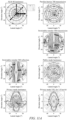
- FIGURES 2A-B are schematic diagrams illustrating in side views a parallax barrier 700 for the privacy display 100 of FIGURES 1A-B .
- FIGURES 2A-B illustrate a cross section in the direction ⁇ in which the apertures 702 are closest.
- monolithic layer 110 Various output layers such as polarisers and retarders that are arranged at the output of the parallax barrier are indicated by monolithic layer 110 for purposes of description.
- Desirable ranges for the structure of the parallax barrier have been established by means of simulation of retarder stacks, parallax barriers, pixel arrangements and experiments with display optical stacks.
- Light rays 710 that are directed along the axis 199 that is normal to the spatial light modulator 48 are directed through the respective aligned aperture 702 of width a.
- the aperture size a is larger than the pixel width w to achieve 100% luminance for head-on directions.
- the apertures 702 have a width a and the pixels 220, 222, 224 have a width w meeting the requirement that: a ⁇ w
- Some light rays 726 are directed in off-axis directions such that the luminance in said off-axis direction is reduced in comparison to the head-on luminance for rays 710.
- the minimum absorption provided by the parallax barrier is desirably 50% so that along the direction in which the apertures 702 are closest, the apertures 702 have a width a, the pixels 220, 222, 224 have a pitch p and the pixels 220, 222, 224 have a width w meeting the requirement that: a ⁇ p ⁇ w / 2
- Some light rays 712 from pixels 220, 222, 224 are incident on the lower side of the parallax barrier absorbing regions 704 and may be absorbed.
- the angle for minimum transmission is provided when the light ray 712 from the centre of the pixel is incident on the centre of the absorbing region 704.
- the polar angle in air ⁇ min may be at least 45 degrees so that along the direction in which the apertures 702 are closest and material between the parallax barrier 700 and the pixels 220, 222, 224 has a refractive index n meeting the requirement that: d ⁇ p ⁇ 2 n 2 ⁇ 1 / 2
- Light rays 716 from the centre of pixels 220, 222, 224 that are incident on the edge of the parallax barrier 700 absorbing region are at the polar angle in air ⁇ max at which the luminance is at most 50% of the head-on luminance. Desirably ⁇ max (in air) is at most 90 degrees and thus the parallax barrier has a separation d from the pixels 220, 222, 224 meeting the requirement that: d ⁇ a ⁇ n 2 ⁇ 1 / 2
- the desirable angle for ⁇ max is preferably at most 60 degrees and thus the parallax barrier has a separation d from the pixels 220, 222, 224 meeting the requirement that: d ⁇ an ⁇ 1 ⁇ 3 / 4 n 2 / ⁇ 3
- TABLE 1 Illustrative dimensions in micrometers for a pixel pitch of 50 micrometers in the direction in which the pixels are closest and refractive index of the medium between the pixel layer 214 and parallax barrier 700 of 1.5 are given in TABLE 1.
- TABLE 1 Pixel pitch, p Pixel width, w Aperture, a Thickness, d Minimum Maximum Minimum Maximum 50 ⁇ m 25 ⁇ m 25 ⁇ m 37.5 ⁇ m 280 ⁇ m 46.8 ⁇ m 50 ⁇ m 3 ⁇ m 3 ⁇ m 48.5 ⁇ m 280 ⁇ m 46.8 ⁇ m
- the thickness, d of the parallax barrier spacer layer 216 is of the order of 30 ⁇ m. Such thickness is typical of typical encapsulation layers for OLED panels as will be described further below.
- Parallax barrier 700 may be formed in desirable proximity to pixel layer 214 to advantageously achieve desirable performance for a switchable privacy display.
- TABLE 2 illustrates a structure for a two view parallax barrier autostereoscopic display for the same pixel pitch and pixel widths wherein the pixel columns are directed to viewing windows, each window providing a left- or right-eye image.
- the ranges of desirable thickness are provided for minimum window size of 60mm, maximum window size 67mm, minimum viewing distance 250mm and maximum window distance 700mm.
- the present embodiments achieve increased luminance and lower thickness than that used for autostereoscopic display.
- Autostereoscopic display parallax barriers do not achieve desirable privacy display luminance control characteristics.
- Some light rays 714 may pass through apertures 702 at angles greater than the critical angle and are thus totally internally reflected. Such rays may be absorbed by the top of the parallax barrier absorbing regions 704. Other absorption mechanisms will be discussed further below.
- the absorbing regions 704 may be partially absorbing. Some light rays 712 may pass through the absorbing regions 704 due to reduced absorption of the absorbing material. Additionally or alternatively the absorbing regions 704 may be arranged with sub-apertures 722 arranged to permit propagation of light rays 712. The sub-apertures 722 may have size and density arranged to provide desirable illumination profile in public mode of operation.
- the barrier regions 704 may transmit 5% of incident light rays by means of sub-apertures 722.
- the luminance at an angle of 60 degrees may be arranged to be 5% by means of control of density and size of sub-apertures 722 and width of aperture for a given pixel pitch p and pixel size a.
- the luminance may be less than 1%.
- Advantageously image visibility in public mode of operation may be increased while high visual security level may be achieved in privacy mode by means of the polar control retarders 300.
- FIGURE 3A is a schematic diagram illustrating in side perspective view the alignment of the parallax barrier 700 with the pixels 220, 222, 224 of FIGURE 1A for a non-pupillated output.
- the parallax barrier 700 directs light from each pixel 220, 222, 224 into a common viewing window 26.
- the common viewing windows are angularly aligned, in other words the common sub-windows 26 from each pixel and aligned barrier aperture 702 overlap at infinity and are collimated.
- the window represents the angular distribution of light from each slit.
- such an arrangement provides similar spatial roll-off across the area of the display 100 as the polar control retarders 300 and polarisers 218, 318. Natural variations of image uniformity across the display area are achieved for a moving observer, that is the part of the display nearest to the user appears the brightest.
- FIGURE 3B is a schematic diagram illustrating in side perspective view the alignment of the parallax barrier 700 with the pixels 220, 222, 224 of FIGURE 1A for a pupillated output.
- the pitch p' along the direction in which the apertures 702 are closest is smaller than the pitch p of the respective aligned pixels 220, 222, 224 along the direction in which the pixels 220, 222, 224 are closest.
- the pitch s' of the apertures 702 are closest is smaller than the pitch s of the respective aligned pixels 220, 222, 224.
- the viewing window 26 is formed at a viewing window plane at distance v that is on the output side of the spatial light modulator 48 such that the common viewing window at which the viewing windows overlap is at a finite distance.
- a head-on observer located at the window plane the luminance uniformity across the area of the display is increased.
- At least some of the apertures of the parallax barrier may comprise a colour filter 703R, 703G, 703B so the apertures of the parallax barrier comprise an array of red, green and blue colour filters.
- the colour filters may correspond to the colour of the respective aligned pixels 220, 222, 224.
- the filters reduce the colour crosstalk from for example blue light leaking into the red pixel aperture advantageously achieving increased colour gamut.
- the apertures 702 may comprise a colour filter for example the apertures 702 corresponding to the red and green emitting pixels 220, 222 may comprise a yellow transmission filter.
- coloured emission may be achieved by for example blue emitting pixels and colour conversion materials aligned to the pixels 220, 222 to achieve coloured output.
- the yellow colour filters of the apertures 702 may provide absorption of residual blue light, advantageously achieving increased colour gamut.
- the materials of the colour filter of the aperture 702 may comprise a non-scattering or low scattering material so that the angular control function of the apertures 702 and absorbing regions 704 is maintained.
- FIGURE 4 is a schematic diagram illustrating in top view an arrangement of uniform emissive pixels 220, 222, 224 and eye spot locations 260, 262, 264 for various polar viewing angles.
- the pixels 220, 222, 224 are arranged in columns and rows, the direction in which the apertures 702 are closest is at 45 degrees with respect to the electric vector transmission direction 219 of the output linear polariser; and each pixel 220, 222, 224 has a light emission region that is a square shape with edges rotated by 45 degrees with respect to the electric vector transmission direction of the output linear polariser.
- the apertures 702 have a square shape with edges rotated by 45 degrees with respect to the electric vector transmission direction of the output linear polariser.
- the eye spot locations 260, 262, 264 represent the image of an observer's pupil at the pixel layer 214 provided by the aperture 702.
- the eye spot location 260 represents the location of a head-on observer's pupil. As the spot location 260 has a size larger than the pixel, the observer sees the same brightness as the pixel brightness and 100% luminance is achieved.
- the observer's eye is located in a display quadrant (with non-zero lateral angle and elevation) and at a transmission minimum.
- the observer's eye is located with zero elevation with a lateral offset and at a transmission minimum.
- the eye spot location 264 has a greater separation from the on-axis location than location 262 so that the transmission minimum is nearest in the quadrant rather than the lateral direction.
- Advantageously suppression in viewing quadrants can be optimised.
- FIGURE 4 achieves desirable rendering of horizontal and vertical lines while reducing the number of red and blue pixels compared to the number of green pixels.
- OLED displays typically provide different emitting areas for red, green and blue pixels due to the different luminous emittance (lumen / mm 2 ) for the respective material systems.
- the pixels 220, 222, 224 of the present disclosure when used with two dimensional aperture 702 arrays comprise emitting regions with substantially the same area for all pixels.
- the variation of white point with viewing angle may be minimised.
- each pixel 220, 222, 224 may be varied by adjusting the drive current between the different coloured pixels so that white point is maintained.
- the green pixels 222 may have for example twice the emitting area than conventionally used.
- the drive current for the green pixels 222 and red pixels 220 may be reduced to achieve desirable white points.
- FIGURE 5 is a schematic diagram illustrating in top view an arrangement of structured emissive pixels 220, 222, 224 and eye spot locations for various polar viewing angles.
- the light emission region of at least some of the pixels comprises light emitting sub-regions 232R, 232G, 232B and non-light emitting sub-regions 234.
- the ratio of the area of light emitting sub-regions to non-light emitting regions is different for red, green and blue pixels 220, 222, 224.
- the sub-regions 232R, 232G, 232B may be provided within the same area for each of the pixels.
- the distribution of sub-regions 232 and eye-spot 260 size may be arranged to provide substantially uniform roll-off of luminance with polar angle to advantageously achieve minimised variation of white point with viewing angle; and desirable drive currents may be provided for each of the colour pixels 220, 222, 224.
- FIGURE 6 is a schematic diagram illustrating in side view the structure of a spatial light modulator 48 and aligned parallax barrier 700 comprising upper ingress reduction layers 750, 752.
- Pixel layer 214 is formed on the substrate 212 and comprises thin film control circuitry 240 that comprises thin film transistors, capacitors, electrodes and other electronic control components. Electrical vias 242 provide connection to electrode 230 that is typically reflective. Emission layers 232R, 232G, 232B are arranged between electron transport layers 236R, 232G, 232B and hole transport layers 238R, 238G, 238B. Transparent electrode 244 is arranged to provide output side electrical connection.
- the emission layer thickness 233R, 233G, 233B and electron transfer layer thickness 237R, 237G, 237B may be adjusted to provide suitable light output characteristics.
- the thickness 233R, 233G, 233B of the light emitting material is different for each of the red, green and blue light emitting regions in pixels 220, 222, 224.
- hole and electron transport layers 236, 238 may be alternatively arranged below and above emission region 232.
- the total thickness of pixel layer 214 may typically be one micron or less, and so differences in location of emission layer 232 are small in comparison to the distance of the spacer layer 216.
- the display 100 device has one or more additional layers 750, 752 arranged in the spacer layer 216 between the pixel layer 214 and the parallax barrier 700, wherein the pixels 220, 222, 224, the one or more additional layers and the parallax barrier 700 are formed as a monolithic stack.
- the one or more additional layers comprise at least one light transmitting inorganic layer 752 arranged to provide a barrier to water and oxygen.
- the material 752 may for example be an oxide material such as SiO x .
- the layers 750 may be provided with an organic material.
- the substrate 212 may be further provided with layers 750, 752 (not shown). Ingress to water and oxygen may be inhibited while maintaining a flexible display structure with desirable mechanical properties. Advantageously display lifetime may be increased.
- the total thickness d may be adjusted to advantageously achieve the desirable luminance roll-off as described elsewhere herein.
- the parallax barrier 700 further comprises at least one light transmitting inorganic material that is arranged to provide a barrier to water and oxygen.
- Advantageously increased lifetime may be provided.
- Further non-transmissive barrier layers may be provided in the absorption regions 704 to achieve increased inhibition to ingress over at least part of the barrier.
- the parallax barrier 700 is arranged between the pixel layer 214 and at least one light transmitting inorganic layer 752 that is arranged to provide a barrier to water and oxygen.
- the inorganic layers 752 are separated by organic layer 750.
- Advantageously high resistance to water and oxygen ingress may be provided in a flexible substrate.
- FIGURE 7 is a schematic diagram illustrating in side view the structure of a spatial light modulator 48 and aligned parallax barrier comprising a glass material 110.
- a glass material 110 may be provided for the cover layer 217 that provides high barrier layer resistance to oxygen and water ingress in comparison to the layers 752, 750 of FIGURE 6 .
- the spacer layer 216 may be provided by an adhesive material or a polymer material. Alternatively the spacer layer 216 may be provided by a glass material which is thinned by chemical-mechanical polishing after fabrication of the backplane 212 and pixel layer 214 to achieve the desirable thickness d.
- FIGURES 8A-C are schematic graphs illustrating the variation of parallax barrier 700 transmission with position for various parallax barrier 700 structures.
- FIGURE 8A illustrates a first transmission profile 701 of relative transmission against position in a direction ⁇ at which the apertures are closest; wherein the absorption regions 704 have 100% absorption.
- Advantageously very low luminance can be achieved in privacy mode at polar angles greater than 45 degrees.
- FIGURE 8B illustrates increased transmission 705 for absorption regions 704, for example by control of the thickness of the material used to form the absorption regions 704.
- the absorption of the region of the parallax barrier 700 between the apertures 702 is less than 100%, and is greater than 80% preferably greater than 90% and more preferably greater than 95%.
- Transmission 705 may for example be less than 5% or less than 2.5%.
- Advantageously increased luminance may be provided at higher polar viewing angles in public mode of operation.
- FIGURE 8C illustrates increased transmission for absorption regions 704 by means of subaperture regions 722 as illustrated in FIGURE 2A for example.
- Average transmission 705 across the light absorbing regions 704 may for example be less than 5% or less than 2.5%.
- Advantageously increased luminance may be provided at higher polar viewing angles in public mode of operation.
- the polar control retarder 300 comprises passive polar control retarder 330 and switchable liquid crystal retarder 301, but in general may be replaced by other configurations of at least one retarder, some examples of which are present in the devices described below.
- FIGURE 9 is a diagram illustrating in perspective side view an arrangement of a switchable polar control retarder 300 comprising a liquid crystal retarder 301 comprising a switchable liquid crystal layer 314 with homogeneous alignment and crossed A-plate polar control retarders 330A, 330B.
- a switchable polar control retarder 300 comprising a liquid crystal retarder 301 comprising a switchable liquid crystal layer 314 with homogeneous alignment and crossed A-plate polar control retarders 330A, 330B.
- TABLE 3 Mode Passive polar control retarder(s) Active LC retarder Type ⁇ n.d /nm Alignment layers Pretilt /deg ⁇ n.d / nm ⁇ Voltage /V Public Crossed A +500 @ 45° Homogeneous 2 750 132 10 Privacy +500 @ 135° Homogeneous 2 23
- the switchable liquid crystal retarder 301 comprises two surface alignment layers 419a, 419b disposed adjacent to the layer of liquid crystal material 421 and on opposite sides thereof and each arranged to provide homogeneous alignment in the adjacent liquid crystal material 421.
- the layer 314 of liquid crystal material 421 of the switchable liquid crystal retarder 301 comprises a liquid crystal material 421 with a positive dielectric anisotropy.
- the passive polar control retarder 330 is provided by a pair of A-plates 330A, 330B that have crossed axes.
- 'crossed' refers to an angle of substantially 90° between the optical axes of the two retarders in the plane of the retarders.
- the angle 310A is at least 35° and at most 55°, more preferably at least 40° and at most 50° and most preferably at least 42.5° and at most 47.5°.
- the angle 310B is at least 125° and at most 145°, more preferably at least 130° and at most 135° and most preferably at least 132.5° and at most 137.5°.
- the passive retarders 330A, 330B may be provided using stretched films to advantageously achieve low cost and high uniformity. Further field of view for liquid crystal retarders with homogeneous alignment is increased while providing resilience to the visibility of flow of liquid crystal material during applied pressure.
- the at least one polar control retarder 300 is arranged, in a first switchable state of the switchable liquid crystal retarder 301, simultaneously to introduce no net relative phase shift to orthogonal polarisation components of light passed by the reflective polariser 302 along an axis 199 along a normal to the plane of the at least one polar control retarder 300 and to introduce a net relative phase shift to orthogonal polarisation components of light passed by the reflective polariser 302 along an axis 197 inclined to a normal to the plane of the at least one polar control retarder 300; and in a second switchable state of the switchable liquid crystal retarder 301, simultaneously to introduce no net relative phase shift to orthogonal polarisation components of light passed by the reflective polariser 302 along an axis 199 along a normal to the plane of the at least one polar control retarder 300 and to introduce no net relative phase shift to orthogonal polarisation components of light passed by the reflective polariser 302 along an axis 197 inclined to a normal to the plane of the
- phase shifts provide polar transmission and reflectivity profiles that achieve (i) high transmission and low reflectivity on-axis; (ii) in a privacy mode reduced transmission and increased reflectivity off-axis; and (ii) in a public mode high transmission and low reflectivity off-axis.
- a switchable privacy display provides high image quality to a head-on user, high visual security level to off-axis snooper and high image visibility to off-axis display users as will now be described.
- FIGURE 10A is a schematic diagram illustrating in side view propagation of output light from a spatial light modulator 48 through the optical stack of FIGURE 1A in a public mode of operation.
- light rays 710 emitted by the pixels 220, 222, 224 and transmitted through the barrier 700 aperture 702 in an on-axis direction have a polarisation state 360 parallel to the electric vector transmission direction 219 of the output polariser 218.
- the on-axis ray 710 then traverses the multiple retarder layers 300 comprising the switchable liquid crystal retarder 301 and the passive retarder 330.
- the switchable liquid crystal retarder 301 is in the off state with a different control voltage across the liquid crystal layer 314.
- the polarised state of the on-axis light ray 710 therefore experiences a retardation when passing through the switchable liquid crystal retarder 301.
- the passive retarder 330 is a C-plate retarder
- the on-axis light ray 710 is propagating in a direction that is substantially parallel to the optical axis of the passive retarder 330.
- the on-axis light ray 710 therefore experiences minimal retardation when passing through the passive retarder 330.
- the combined effect off the plurality of retarders 300 results in the on-axis light ray 710 exiting the plurality of retarders 300 with the same or similar linear polarisation state 362 to the linear polarisation state 360 with which the on-axis light ray 710 entered the plurality of retarders 300.
- This linear polarisation state 362 is parallel to the electric vector transmission direction 319 of the additional polariser 318 and the on-axis ray 710 therefore exits the display device 100 with a relatively unmodified luminance.
- the off-axis ray 726 that is transmitted by the barrier 700 aperture 702 traverses the plurality of retarders 300 in a similar fashion to the on-axis ray 710.
- the plurality of retarders 300 provides no overall transformation of polarisation states 360, 361 of light ray 710 passing therethrough perpendicular to the plane of the switchable retarder or light ray 726 passing therethrough at an acute angle to the perpendicular to the plane of the switchable retarder 301.
- Polarisation state 362 is substantially the same as polarisation state 360 and polarisation state 364 is substantially the same as polarisation state 361.
- the angular transmission profile is substantially uniformly transmitting across a wide polar region.
- the plural retarders 300 provide no overall retardance to light passing therethrough perpendicular to the plane of the retarders or at an acute angle to the perpendicular to the plane of the plural retarders 300.
- the variation of display luminance with viewing angle in the first state is substantially unmodified. Multiple users may conveniently view the display from a wide range of viewing angles.
- FIGURE 10B is a schematic diagram illustrating in side view propagation of light rays from an ambient light source 604 through the optical stack of FIGURE 1A in a public mode of operation.
- the on-axis ray 410 of ambient light 604 traverses the plurality of retarders 300 in a similar fashion to the on-axis ray 710 emitted from the emissive pixels 220, 222, 224 discussed above.
- the on-axis ray 410 traverses the plurality of retarders 300 in the reverse direction to the on-axis ray 710 emitted from the emissive pixels 220, 222, 224
- the traversal of the plurality of retarders 300 in a reverse direction may not change the effect of the plurality of retarders 300 on the light ray as discussed above for light emitted from the emissive pixels 220, 222, 224.
- the on-axis ray 410 therefore reaches the parallax barrier 700 absorption regions 704 whereon it is absorbed; or the pixel layer 214 whereon it may be absorbed or reflected as will be described further below.
- the off-axis ray 412 experiences no overall transformation of polarisation state when passing through the plurality of retarders 300.
- Ambient light 604 is unpolarised and the off-axis light ray initially has no polarisation 370.
- the additional polariser 318 passes the polarisation component 372 that is parallel to the electric vector transmission direction 319 of the additional polariser.
- the additional polariser 318 absorbs the majority of the polarisation state 372 that is perpendicular to the electric vector transmission direction 319 of the additional polariser 318.
- Some light is reflected from the front surface of the polariser 318 by Fresnel reflections at the outer air interface.
- the linear polarisation state 374 of the off-axis ray 412 is therefore parallel to the electric vector transmission direction 303 of the reflective polariser 302 and the off-axis ray is not reflected but instead passes the reflective polariser 302 to reach the parallax barrier 700 where it may be absorbed by the parallax barrier absorption regions or transmitted to the pixel layer 214. Some of the reflected light rays 412 will be further absorbed by the absorption regions 704 of the parallax barrier 700 as further described below.
- the display reflectance in the public mode is reduced across a wide range of viewing angles. Multiple users may conveniently view the display from a wide range of viewing angles with high image contrast.
- FIGURE 10C is a schematic diagram illustrating in side view propagation of output light from a spatial light modulator 48 through the optical stack of FIGURE 1A in a privacy mode of operation.
- the switchable liquid crystal retarder 301 In the privacy mode, the switchable liquid crystal retarder 301 is in the on state where a voltage is applied to the liquid crystal layer 314. The switchable liquid crystal retarder 301 may therefore be in the second state of the said two states. In the case where the switchable liquid crystal retarder 301 has a positive dielectric anisotropy, the switchable liquid crystal retarder 301 therefore acts in the second state in a similar manner to adjust the phase of the incident polarisation state that is output.
- the on-axis light ray 710 experiences no retardation when passing through the switchable liquid crystal retarder 301 in the second state, and therefore the linear polarisation state 360 of the on-axis light ray 710 prior to traversing the plurality of retarders 300 is the same as the linear polarisation state 362 after traversing the plurality of retarders 300.
- the on-axis ray 710 therefore exits the display via the additional polariser 318 with a largely unchanged luminance in the privacy mode of operation.
- the off-axis light ray 726 therefore arrives at the additional polariser 318 with a linear polarisation state 364 that is at least partially rotated when compared to the linear polarisation state 361.
- the linear polarisation state 364 has at least some perpendicular component to the electric vector transmission direction 319 of the additional polariser 318 and the luminance of the off-axis light ray 726 is therefore reduced compared to the on-axis ray 710.
- the display luminance at wide viewing angles may be reduced in the second state. Snoopers may therefore be prevented from viewing the image emitted by the display device 100 at wide viewing angles. Stray light may be reduced in night-time operation while the head-on user may see an image.
- FIGURE 10D is a schematic diagram illustrating in side view propagation of light rays from an ambient light source 604 through the optical stack of FIGURE 1A in a privacy mode of operation.
- incident on-axis light rays 410 from the ambient light source 604 traverse the plurality of retarders 300 in a similar fashion to the on-axis ray 710 emitted from the emissive pixels 220, 222, 224 as described in relation to FIGURE 10C .
- the on-axis ray 410 traverses the plurality of retarders 300 in the reverse direction to the on-axis ray 710 emitted from the emissive pixels 220, 222, 224
- the direction of traversal of the plurality of retarders 300 into or out of the display does not change the effect of the plurality of retarders 300 on the light ray as discussed for light emitted from the emissive pixels 220, 222, 224.
- the on-axis ray 410 therefore reaches the parallax barrier 700 where it may be absorbed by the parallax barrier absorption regions or transmitted to the pixel layer 214. Some of the reflected light rays 412 will be further absorbed by the absorption regions 704 of the parallax barrier 700 as further described below.
- off-axis light rays 412 experience a transformation of polarisation when passing through the material 414 of the switchable liquid crystal retarder 301. This is because of the acute angle of entry of the off-axis light ray 412, as discussed in further detail below.
- the off-axis light ray 412 therefore arrives at the reflective polariser 302 with a linear polarisation state 374 that is at least partially rotated when compared to the linear polarisation state 372.
- the linear polarisation state 374 has at least some perpendicular state to the electric vector transmission direction 303 of the reflective polariser 302 and is therefore at least partially reflected by the reflective polariser 302.
- the ray 412 then traverses the plurality of retarders 300 in the reverse direction, reversing the polarisation conversion from the first pass of the plurality of retarders 300 and resulting in a polarisation state 376 that is parallel to the electric vector transmission direction of the additional polariser 318.
- the off-axis ray 412 therefore leaves the display device 100 with polarisation state 378, resulting in the stack appearing as a mirror when viewed from a wide-angle.
- the additional polariser 318 absorbs the majority of the polarisation state 372 that is perpendicular to the electric vector transmission direction 319 of the additional polariser, but may reflect a small proportion of the perpendicular state 404.
- the reflectance at wide viewing angles may be increased in the second state. Snoopers may therefore be prevented from viewing the image emitted by the display device 100 at wide viewing angles due to the reflected light reducing the contrast of the image being emitted by the display device, and so increasing visual security level, VSL as described in eqn. 7, above due to increased reflectivity, R.
- FIGURE 11A is a polar plot array for the component contributions and output of the arrangement of FIGURE 1A comprising polar plots for spatial light modulator 48 luminance, parallax barrier 700 transmission, switchable retarder 300 transmission, normalised switchable retarder 300 reflection, public mode luminance, privacy mode luminance and visual security level for a lux/nit ratio of 1.0; and
- FIGURE 11B is a linear profile plot array for the component contributions and output of the arrangements of FIGURE 11A comprising linear profiles at azimuthal angles of 0 degrees (Eastern direction), 90 degrees (Northern direction), 45 degrees (North Eastern direction) and 225 degrees (South Western direction). For purposes of the current description, the azimuthal orientations of the profiles in FIGURE 11B are illustrated on the SLM luminance plot of FIGURE 11A .
- Illustrative parallax barrier 700 and OLED pixel parameters for FIGURES 11A-B are provided in the first row of TABLE 4 with reference to the pitch, p of 50 ⁇ m in the direction in which the pixels are closest.
- the pixels 220, 222, 224 are provided in the diamond arrangement of FIGURE 4 .
- the direction in which the pixels are closest is for an azimuth of 45 degrees. TABLE 4 FIGS.
- a peak eQM reflectivity of 36% is used which corresponds to the 100% contour on the plot of normalised switchable retarder reflection after taking into account polariser 318 transmission and reflective polariser 302 reflectance to polarised light.
- the SLM 48 luminance plot illustrates that OLED displays provide a non-Lambertian luminance roll-off typically with greater than 20% of head-on luminance provided at polar angles of 50 degrees.
- the parallax barrier 700 transmission plot illustrates the difference in profiles for 0 degrees and 45 degrees azimuths due to the different separations of the pixels in this orientation.
- the switchable retarder 300 transmission and reflectivity plots illustrate the control of phase is along the lateral direction using the structure of FIGURE 9 .
- the public mode illuminance is determined by the transmission by the parallax barrier 700 of the light from the spatial light modulator 48.
- the switchable polar control retarder 300 provides only a small modulation of this luminance profile.
- the privacy mode luminance illustrates that less than 1% luminance is provide in the lateral direction and in upper viewing quadrants.
- the display has high visibility for 0 degrees lateral angle and for rotations about the horizontal axis.
- a comfortable viewing angle may be set for viewing the display from an on-axis position by the user.
- FIGURE 11C is a polar profile plot and linear polar profile plot for the illustrative embodiment of FIGURES 11A-B with a lux/nit ratio of 0.25.
- the display 100 properties are described in the second row of TABLE 4.
- the visual security level (VSL) plots are dependent on the ambient illuminance condition.
- the ambient illuminance is provided as a ratio of head-on luminance.
- a display with 300nit head-on luminance and ambient illuminance falling on to the display of 300 lux has a lux/nit ratio of 1.0.
- a head-on luminance of 100 nits may be provided for an ambient illuminance of 25nits, providing a lux/nit ratio of 0.25.
- the switchable reflectivity of the present embodiment achieves increased visual security level at low lux/nit ratios. Further the parallax barrier 700 may further reduce the off-axis luminance to advantageously achieve further increased visual security in low illuminance conditions.
- the visual security level line profiles of FIGURES 11B-C illustrate that a visual security level of greater than 4.0 may be achieved for lateral angles and in viewing quadrants at lateral angles of at least 45 degrees and for azimuthal angles in the lateral direction and in the viewing quadrants in illumination conditions of less than 0.25 lux/nit.
- Advantageously high visual security level may be achieved for off-axis users over a wide range of polar locations. The visual security level does not degrade at higher polar angles in the lateral direction.
- FIGURE 12A is a polar plot array for the component contributions and output of the arrangement of FIGURE 1A for an illustrative arrangement in which the parallax barrier 700 is removed comprising polar plots for spatial light modulator 48 luminance, parallax barrier 700 transmission, switchable retarder transmission, switchable retarder reflection, public mode luminance, privacy mode luminance and visual security level at 1.0 lux/nit; and
- FIGURE 12B is a linear profile plot array for the component contributions and output of the arrangements of FIGURE 12A comprising linear profiles at azimuthal angles of 0, 90, 45 and 225 degrees.
- the display 100 properties are described in the third row of TABLE 4.
- the polar control retarders 300 may not achieve desirable visual security levels in displays with the high off-axis luminance levels as are typically provided by emissive spatial light modulators 48 in which the parallax barrier 700 is not present.
- VSL falls below 4.0 for 1.0 lux/nit.
- Such an arrangement provides undesirable visual security to an off-axis snooper despite having high VSL at angles around 45 degrees.
- FIGURE 13A is a polar plot array for the component contributions and output of the arrangement of FIGURE 1A for an illustrative arrangement in which the switchable retarder is removed comprising polar plots for spatial light modulator 48 luminance, parallax barrier 700 transmission, switchable retarder transmission, switchable retarder reflection, public mode luminance, privacy mode luminance and visual security level for 1.0 lux/nit; and
- FIGURE 13B is a linear profile plot array for the component contributions and output of the arrangements of FIGURE 13A comprising linear profiles at azimuthal angles of 0, 90, 45 and 225 degrees.
- the parallax barrier thickness 700 is designed to be the minimum thickness to provide a VSL of greater than 4.0 at at least one azimuth for a polar angle of 45 degrees in the lateral direction.
- Such a display has undesirable privacy performance over a wide range of polar viewing angles and in particular viewing quadrants without substantial reduction in aperture size and subsequent undesirable loss of transmission efficiency.
- FIGURE 14 is a schematic diagram illustrating in side view reflection of ambient light in the display 100 of FIGURE 1A .
- Features of the arrangement of FIGURE 14 not discussed in further detail may be assumed to correspond to the features with equivalent reference numerals as discussed above, including any potential variations in the features.
- Light rays 710 are passed by linear polarisers 218, 318 with a spectral modification of light from the pixels 220, 222, 224 provided by the spectral transmission of the polarisers 218, 318.
- Light rays 714, 715 that are internally reflected from the outer surface of the display 100 Light rays 714 are absorbed at incidence are directed on to the parallax barrier 700 absorbing regions 704. Light rays 715 are reflected from the reflective pixel layer 214.
- the reflection reduction quarter-wave retarder 228 provides circular polarisation state 442 that undergoes a phase change at reflection to provide circular polarisation state 444 after reflection which is converted to a polarisation state that is orthogonal to the direction 219 and is absorbed.
- the parallax barrier 700 is arranged to absorb light incident thereon. Light rays 410 from ambient source 604 are passed by polarisers 218, 318 and absorbed by barrier regions 704. Light rays 412 that pass through the barrier and are reflected may be absorbed by the barrier after reflection.
- the display 100 device is for use in ambient illumination 604 and the parallax barrier 700 absorbs at least some of the ambient illumination 604 light rays 412 transmitted through the apertures 702 that is reflected from the pixel layer 214.
- FIGURE 15 is a schematic graph illustrating the variation of output luminance with wavelength for a case that the additional polariser 318 is a broadband absorbing polariser and for a case that the additional polariser 318 is a leaking absorbing polariser.
- Profile 870 illustrates the variation of transmitted luminance by parallel broadband polarisers;
- profile 872 illustrates the variation of transmitted luminance by parallel leaking polarisers;
- profile 874 illustrates the variation of transmitted luminance by crossed broadband polarisers;
- profile 876 illustrates the variation of transmitted luminance by crossed leaking polarisers.
- the leaking polariser 318 has increased leakage in the blue spectral band and increased transmission.
- the output polariser 218 and additional polariser 318 when crossed with a second notional polariser of the same material has transmission for wavelengths from 520nm to 560nm that is less than the transmission for wavelengths from 450nm to 490nm.
- the transmission for wavelengths from 450nm to 490nm is greater than 1%, preferably greater than 2% and most preferably greater than 3%; and the transmission for wavelengths from 520nm to 560nm is less than 3%, preferably less than 2% and most preferably less than 1%.
- FIGURE 16A is a schematic graph illustrating the variation of polariser 218, 318 transmission with wavelength for broadband absorbing polarisers and for leaking absorbing polarisers and with respect to the spectral outputs 890R, 890G, 890B of red, green and blue emitting pixels 220, 222, 224 for transmitted rays 710 of FIGURE 14 .
- Profile 882 illustrates the spectral transmission of the embodiment of FIGURE 1A comprising leaking polarisers 218, 318.
- profile 880 illustrates the spectral transmission of the embodiment of FIGURE 1A comprising broadband absorbing polarisers 218, 318.
- profile 882 achieves substantially higher transmission in the red, green and blue channels in comparison to arrangements comprising broadband polarisers 218, 318.
- profile 870 illustrates the spectral output of a display that comprises a broadband absorbing polariser and broadband reflectance control quarter-wave retarder and does not comprise barrier 700, polar control retarder 300 or additional polariser 318.
- profile 882 has substantially the same transmission for blue light as a display not comprising additional polariser 318. Efficient blue light emission provides increased lifetime for OLED displays.
- the present embodiment achieves the same display lifetime as for conventional displays without additional polariser 318.
- FIGURE 16B is a schematic graph illustrating the variation of reflectance with wavelength for broadband absorbing polarisers 218, 318 and for leaking absorbing polarisers 218, 318 and with respect to the spectral output 890R, 890G, 890B of red, green and blue emitting pixels 220, 222, 224 for reflected rays of FIGURE 14 .
- Reflectance is determined at least in part by the transmission of light rays 440 in FIGURE 14 through polarisers 218, 318 after reflection reduction quarter-wave retarder 228 and by absorption of parallax barrier 700.
- the aperture ratio of the parallax barrier is 25% so that the barrier absorption is 75% for light rays 410, 412 of FIGURE 14 .
- 318 profile 888 illustrates the average spectral transmission of the display integrated over viewing angles.
- Advantageously very low average reflectance may be provided by the display. Further display efficiency is increased as illustrated in FIGURE 16A .
- Profile 884 illustrates the spectral transmission of the display of FIGURE 14 for light rays 440 that are both transmitted and reflected by aperture 702 of the parallax barrier 700.
- Profile 884 has significantly improved extinction in comparison to profile 876 with leakage at the peak blue spectral wavelength of less than 1%.
- low reflectivity is achieved.
- profile 886 illustrates the spectral output of a display that comprises a broadband absorbing polariser and broadband reflectance control quarter-wave retarder and does not comprise barrier 700, polar control retarder 300 or additional polariser 318.
- a display achieves low reflectance over a wide spectral range but has reduced spectral transmission.
- profile 876 illustrates the spectral output of a display that comprises a leaking absorbing polariser and broadband reflectance control quarter-wave retarder and does not comprise barrier 700, polar control retarder 300 or additional polariser 318.
- a display achieves low reflectance over a wide spectral range.
- Such a display provides undesirable reflectance of light, particularly in the blue and green parts of the spectrum. Leaking polarisers with spectral transmission profiles 872, 876 are thus not suitable for reflectance control in emissive displays.
- FIGURE 17A is a schematic diagram illustrating in side perspective view a switchable privacy display 100 for use in ambient illumination 604 comprising a micro-LED emissive spatial light modulator 48, parallax barrier 700, output polariser 218 and reflection control quarter-wave retarder 228, passive polar control retarder 380, reflective polariser 302, a switchable polar control retarder 300 and an additional polariser 318 arranged on the output side of the spatial light modulator 48; and
- FIGURE 17B is a schematic diagram illustrating in front view alignment of optical layers in the optical stack of FIGURE 17A .
- FIGURES 18A-B not discussed in further detail may be assumed to correspond to the features with equivalent reference numerals as discussed above, including any potential variations in the features.
- pixels 220, 222, 224 comprising inorganic micro-LEDs may have luminous emittance (lm/mm 2 ) that is more than 10 3 greater.
- the area of micro-LED pixels 220, 222, 224 may be significantly smaller than that used for OLED pixels 220, 222, 224.
- Further smaller micro-LED pixels 220, 222, 224 are lower cost due to reduced monolithic semiconductor area usage.
- micro-LEDs may have a width or diameter of less than 5 micrometers for a pixel pitch of 50 micrometers in the direction in which the pixels are closest.
- the pixel layer 214 may comprise a light absorbing material 227 to advantageously achieve reduced reflectance in comparison to the reflective pixel layer typical of OLED pixel layers 214 of FIGURE 1A .
- FIGURE 17A further differs from FIGURE 1A in comprising apertures 702 with a circular shape.
- Advantageously transmission profile symmetry may be increased.
- the pixels 220, 222, 224 are arranged on a square grid rather than diamond grid. Such an arrangement provides for reduced luminance in the lateral direction with increased luminance in the quadrants.
- Advantageously visual security level in privacy mode may be increased for small elevations as will be illustrated below.
- displays comprising mixtures of OLED and micro-LED pixels may be provided (not shown).
- blue micro-LEDs may be provided and green and blue OLED pixels.
- Advantageously blue lifetime may be increased and colour conversion for micro-LEDs is not used.
- FIGURE 17C is a schematic diagram illustrating in top view an arrangement of micro-LED emissive pixels 220, 222, 224 and eye spot locations for various polar viewing angles.
- FIGURE 17D is a schematic diagram illustrating in side perspective view the passive polar control retarder 380 arranged between the output polariser 218 and reflective polariser 302.
- Passive polar control retarder 380 is arranged between the output polariser 218 and reflective polariser 302.
- the passive polar control retarder 380 is capable of simultaneously introducing no net relative phase shift to orthogonal polarisation components of light rays passed by the output polariser 218 along an axis 199 along a normal to the plane of the at least one polar control retarder 380 and introducing a relative phase shift to orthogonal polarisation components of light passed by the reflective polariser 302 along an axis 197 inclined to a normal to the plane of the at least one polar control retarder 380.
- the at least one passive retarder 380 comprises a retarder material 430 having its optical axis 431 perpendicular to the plane of the retarder, the at least one passive retarder 330 having a retardance for light of a wavelength of 550nm in a range from -150nm to -900nm, preferably in a range from -200nm to -500nm and most preferably in a range from -250nm to -400nm.
- FIGURE 18A is a schematic diagram illustrating in side view the structure of a spatial light modulator and aligned parallax barrier comprising vignetted parallax barrier apertures.
- the apertures 702 have an absorption that has a transmission gradient at the edges of the aperture 702 that has a transmission gradient width ⁇ of greater than 1 micron, preferably greater than 2 microns and more preferably greater than 3 microns.
- a point emitter 720 within the pixel 222 emits a spherical wavefront 711 towards the aperture 702.
- residual wavefront curvature results in near field Fresnel diffraction such that rays 714 are provided at unintended angles in the far field.
- such rays may provide undesirable polar luminance variations from a point source and provide visible uniformity variations that can be seen by an observer across the area of the display 100.
- the separation p of pixels may be 50 micrometers and the pixel width may be 3 micrometers. In an illustrative OLED embodiment, the separation p of pixels may be 50 micrometers and the pixel width may be 25 micrometers. In both arrangements the aperture 702 width a may be 16 micrometers.
- the diffracted rays are blurred due to the convolution with the large pixel area.
- Advantageously high display uniformity may be achieved.
- the convolution blurring in OLED arrangements may be substantially greater than for micro-LED displays due to the small size of the micro-LED emitters 220, 222, 224.
- the transmission gradient width ⁇ provides diffractive apodisation of diffracted rays 714 in particular for small emitting areas such as micro-LEDs in which substantial convolution blurring is not provided.
- the luminance variations from the diffracted rays 714 are reduced by the transmission gradient width ⁇ .
- Advantageously the visibility of spatial luminance variations across the display using micro-LED pixels 220, 222, 224 is reduced.
- FIGURES 18B-D are schematic graphs illustrating the variation of parallax barrier transmission with position for various parallax barrier 700 structures.
- FIGURE 18B illustrates a first apodised transmission profile 701 of relative transmission against position in a direction ⁇ at which the apertures are closest; wherein the absorption regions 704 have 100% absorption.
- the slope may be formed by thickness variations of absorbing material and/or by half tone patterning across the width ⁇ .
- Advantageously luminance variations across the display may be minimised.
- the transmission varies to apodise the output as described with reference to FIGURE 18A .
- FIGURE 18C illustrates increased transmission 705 for absorption regions 704, for example by control of the thickness of the material used to form the absorption regions 704.
- the absorption of the region of the parallax barrier 700 between the apertures 702 is less than 100%, and is greater than 80% preferably greater than 90% and more preferably greater than 95%.
- Transmission 705 may for example be less than 5% or less than 2.5%.
- Advantageously increased luminance may be provided at higher polar viewing angles in public mode of operation.
- FIGURE 18D illustrates increased transmission for absorption regions 704 by means of subaperture regions 722 as illustrated in FIGURE 2A for example.
- Average transmission 705 across the light absorbing regions 704 may for example be less than 5% or less than 2.5%.
- Advantageously increased luminance may be provided at higher polar viewing angles in public mode of operation.
- FIGURE 19A is a polar plot array for the component contributions and output of the arrangement of FIGURE 17A omitting the passive polar control retarder 380 comprising polar plots for spatial light modulator 48 luminance, parallax barrier 700 transmission, switchable retarder 300 transmission, normalised switchable retarder 300 reflection, public mode luminance, privacy mode luminance and visual security level for a lux/nit ratio of 1.0; and
- FIGURE 19B is a linear profile plot array for the component contributions and output of the arrangements of FIGURE 19A .
- Illustrative parallax barrier 700 and micro-LED pixel 220, 222, 224 parameters for FIGURES 19A-B are provided in the first row of TABLE 5 with reference to the pitch, p of 50 ⁇ m in the direction in which the pixels are closest.
- the pixels 220, 222, 224 are provided in the square packed arrangement of FIGURE 17C and square parallax barrier 700 apertures 702 are provided (in comparison to the illustrated circular apertures).
- the direction in which the pixels are closest is for an azimuth of 0 degrees.
- the luminance profile from the micro-LED pixels 220, 222, 224 is illustrated as Lambertian and thus higher levels of luminance are provided at higher polar angles.
- the polar output profile from the parallax barrier 700 has a high central output region and then slopes to 5% luminance at high polar angles using for example the arrangements of FIGURE 2A .
- the public mode of operation retains desirable image visibility at high viewing angles.
- the slope of the luminance roll-off in public mode is determined by the profile of the barrier edge which in the present illustrative embodiment is hard-edged.
- the soft-edged parallax barriers of FIGURES 18A-D may further achieve a smoother roll-off of luminance profile in public mode of operation.
- Advantageously luminance uniformity for head-on use, and uniformity for off-axis polar viewing regions is improved.
- a visual security level of greater than 4.0 is achieved for polar angles above 45 degrees and in particular in the viewing quadrants.
- the visual security level may be further increased by reducing the transmission level of the parallax barrier 700 absorption regions 704.
- FIGURE 19C is a polar plot array for the component contributions and output of the arrangement of FIGURE 17A comprising polar plots for spatial light modulator 48 luminance, parallax barrier 700 light absorbing region 704 transmission, passive polar control retarder 380 transmission, switchable retarder 300 transmission, switchable retarder 300 reflection, public mode luminance, privacy mode luminance and visual security level; and
- FIGURE 19D is a linear profile plot array for the component contributions and output of the arrangements of FIGURE 19C comprising linear profiles at azimuthal angles of 0, 90, 45 and 225 degrees.
- the display 100 properties are described in the second row of TABLE 5.
- the passive polar control retarder 380 reduces the luminance in the viewing quadrants.
- the visual security levels in the viewing quadrants may be improved.
- FIGURE 20A is a polar plot array for the component contributions and output of the arrangement of FIGURE 17A for an illustrative arrangement in which the parallax barrier 700 is removed comprising polar plots for spatial light modulator 48 luminance, parallax barrier 700 light absorbing region 704 transmission, switchable retarder 300 transmission, switchable retarder 300 reflection, public mode luminance, privacy mode luminance and visual security level; and
- FIGURE 20B is a linear profile plot array for the component contributions and output of the arrangements of FIGURE 20A comprising linear profiles at azimuthal angles of 0, 90, 45 and 225 degrees.
- the display 100 properties are described in the third row of TABLE 5.
- the polar control retarders 300 may not achieve desirable visual security levels in displays with the high off-axis luminance levels as are typically provided by emissive spatial light modulators 48 comprising micro-LEDs in which the parallax barrier 700 is not present.
- VSL linear polar profile plot of visual security level in the lateral (0 degrees) direction at angles of greater than 60 degrees
- VSL remains below 4.0 for 1.0 lux/nit for almost all polar viewing angles.
- Such an arrangement provides undesirable visual security to an off-axis snooper.
- FIGURE 21A is a polar plot array for the component contributions and output of the arrangement of FIGURE 17A for an illustrative arrangement in which the switchable retarder 300 and passive polarisation control retarder 380 are removed and the parallax barrier 700 provides transmission in the light absorbing regions 704; comprising polar plots for spatial light modulator 48 luminance, parallax barrier 700 transmission, switchable retarder 300 transmission, switchable retarder 300 reflection, public mode luminance, privacy mode luminance and visual security level; and FIGURE 21B is a linear profile plot array for the component contributions and output of the arrangements of FIGURE 21A comprising linear profiles at azimuthal angles of 0, 90, 45 and 225 degrees.
- the display 100 properties are described in the fourth row of TABLE 5. To achieve desirable image visibility in public mode, the luminance at high polar viewing angles is 5%. However, the visual security level is below 4.0 for all polar viewing angles and below 2.0 for most polar viewing angles. Such a display does not provide a satisfactory privacy mode of operation.
- FIGURE 21C is a polar plot array for the component contributions and output of the arrangement of FIGURE 17A for an illustrative arrangement in which the switchable retarder 300 and passive polarisation control retarder 380 are omitted and the parallax barrier 700 provides no transmission in the light absorbing regions 704; comprising polar plots for spatial light modulator 48 luminance, parallax barrier 700 transmission, switchable retarder 300 transmission, switchable retarder 300 reflection, public mode luminance, privacy mode luminance and visual security level; and FIGURE 21D is a linear profile plot array for the component contributions and output of the arrangements of FIGURE 21C comprising linear profiles at azimuthal angles of 0, 90, 45 and 225 degrees.
- the display 100 properties are described in the fifth row of TABLE 5.
- the luminance at high polar viewing angles is 0%, that is the absorbing regions 704 are highly absorbing.
- Such a display does not provide a satisfactory public mode of operation. Transmission levels between 0% and 5% do not provide satisfactory trade-offs between privacy and public modes of operation.
- the present embodiments achieve high visual security level over a wide polar range in privacy mode and achieve high image visibility of a wide polar range in public mode. Further high head-on image visibility is achieved in both privacy and public modes of operation.
- FIGURE 22A is a diagram illustrating in perspective side view an arrangement of a switchable retarder in a privacy mode wherein the switchable retarder comprises a switchable LC layer with homogeneous alignment arranged between C-plate passive polar control retarders 330A, 330B; and FIGURE 22B is a diagram illustrating in perspective side view an arrangement of a switchable retarder in a public mode wherein the switchable retarder comprises a switchable LC layer with homogeneous alignment arranged between C-plate passive polar control retarders 330A, 330B.
- FIGURES 22A-B not discussed in further detail may be assumed to correspond to the features with equivalent reference numerals as discussed above, including any potential variations in the features.
- the retarders 330A, 330B may comprise the substrates for the switchable liquid crystal layer 314. Advantageously thickness may be reduced. Further, flexible substrates may be provided.
- the display 100 may be provided in active flexible embodiments (bendable multiple times by the user) or in passive flexible embodiments (bendable during manufacturing) to achieve free-form display profiles.
- FIGURE 23A is a schematic diagram illustrating in perspective side view an arrangement of retarder layers arranged between parallel polarisers and comprising a 270 degree supertwisted switchable liquid crystal retarder 301 arranged between quarter-wave plates.
- FIGURES 23A-C not discussed in further detail may be assumed to correspond to the features with equivalent reference numerals as discussed above, including any potential variations in the features.
- Further embodiments of polar control retarders that achieve symmetric polar profiles are described in U.S. Patent Publ. No. 2020-0159055 , which is herein incorporated by reference in its entirety.
- First and second quarter-wave plates 296A, 296B are arranged between the additional polariser 318 and the output polariser 218.
- the first quarter-wave plate 296A is arranged on the input side of the second quarter-wave plate 296B and is arranged to convert a linearly polarised polarisation state passed by the output polariser 218 on the input side thereof into a circularly polarised polarisation state.
- the second quarter-wave plate 296B on the output side being arranged to convert a circularly polarised polarisation state that is incident thereon into a linearly polarised polarisation state that is passed by the additional polariser 318 on the output side thereof.
- At least one retarder 301 is arranged between the pair of quarter-wave plates 296A, 296B.
- the at least one polar control retarder 300 comprises a switchable liquid crystal retarder 301 comprising a layer of liquid crystal material and electrodes arranged to apply a voltage for switching the layer of liquid crystal material.
- the layer of liquid crystal material has a twist of 360 degrees and a retardance for light of a wavelength of 550nm in a range from 1 100nm to 1400nm and most preferably in a range from 1150nm to 1300nm.
- FIGURE 23B is a polar plot array for the component contributions and output of the arrangement of FIGURE 17A omitting the passive polar control retarder 380 comprising polar plots for spatial light modulator 48 luminance, parallax barrier 700 transmission, switchable retarder 300 transmission, normalised switchable retarder 300 reflection, public mode luminance, privacy mode luminance and visual security level for a lux/nit ratio of 1.0; and
- FIGURE 23C is a linear profile plot array for the component contributions and output of the arrangements of FIGURE 23A .
- An illustrative liquid crystal retarder 300 is described in TABLE 6.
- An illustrative parallax barrier 700 and OLED pixel 220, 222, 224 for FIGURES 23B-C is described in TABLE 7 with reference to the pitch, p of 50 ⁇ m in the direction in which the pixels are closest.
- the pixels 220, 222, 224 are provided in the square packed arrangement of FIGURE 4 and square parallax barrier 700 apertures 702 are provided.
- the direction in which the pixels are closest is for an azimuth of 0 degrees.
- a rotationally symmetric privacy mode may be achieved in comparison to the laterally symmetric profiles achieved by the embodiments using polar control retarders 300 such as those of FIGURE 9 for example.
- FIGURE 24A is a schematic diagram illustrating in perspective views the appearance of luminance of a mobile device in public mode comprising the display device 100 of FIGURE 1A with the switchable polar control retarder 300 of FIGURE 23 with appearance shown in order from top left clockwise: head-on landscape, head-on portrait, look-down portrait and look-from-right landscape.
- the viewing direction along axis 199 of the display device 100 is perpendicular to the viewing surface of the display device 100.
- the image being emitted by the display device 100 is visible to an observer as represented by the white colouring representing the image emitted by the display device 100.
- the image is visible in all of an on-axis landscape and portrait orientation 520, a look-down portrait orientation 522 and a look-from-right landscape orientation 528.
- FIGURE 24B is a schematic diagram illustrating in perspective views the appearance of luminance of a mobile device in privacy mode comprising the display device 100 of FIGURE 1A with the switchable polar control retarder 300 of FIGURE 23 with appearance shown in order from top left clockwise: head-on landscape, head-on portrait, look-down portrait and look-from-right landscape.
- the view to an observer remains unchanged in the on-axis landscape and portrait orientation 520 and the image emitted by the display device 100 is visible to an observer.
- the look-down portrait orientation 522 and the look-from-right landscape orientation 528 the image emitted by the display device is no longer visible.
- a snooper observing from a wide-angle instead observes a mirror-like surface provided by the reflective polariser 302 as described above.
- FIGURE 24C is a schematic diagram illustrating in perspective views the appearance of reflectivity of a mobile device in privacy mode comprising the display device 100 of FIGURE 1A with the switchable polar control retarder 300 of FIGURE 23 with appearance shown in order from top left clockwise: head-on landscape, head-on portrait, look-down portrait and look-from-right landscape.
- the view to an observer remains unchanged in the on-axis landscape and portrait orientation 520 as the reflectivity from the additional polariser 318 is minimal.
- reflections from the surface of the additional polariser 318 may result in frontal reflections as described above, desirably increasing visual security level, VSL.
- FIGURE 25A is a schematic diagram illustrating in top view an automotive vehicle 600 with a switchable directional display 100 arranged within the vehicle cabin 602 in a night mode of operation.
- the night mode of the switchable directional display 100 may correspond to the privacy mode discussed above.
- a light cone 620 (for example representing the cone of light within which the luminance is greater than 50% of the peak luminance emitted by the switchable directional display 100) may indicate the range of angles in which the image emitted by the switchable directional display 100 is discernible.
- the driver 604 falls within the area defined by the light cone 620 in a horizontal direction and the image emitted by the switchable directional display 100 is therefore discernible to the driver 604.
- high-angle light rays 622 falling outside the light cone 620 in a horizontal direction have a reduced luminance and the image emitted by the switchable directional display 100 therefore may not be discernible to a passenger 608 in the vehicle 600. This may be advantageous if the passenger is attempting to sleep or relax during the night.
- the reflective polariser 302 may be omitted if some image visibility to other users is acceptable.
- Advantageously display efficiency may be increased and visibility of stray light reduced.
- FIGURE 25B is a schematic diagram illustrating in side view an automotive vehicle 600 with a switchable directional display 100 arranged within the vehicle cabin 602 in a night mode of operation.
- the volume 606 occupied by the face of the driver falls within the area defined by the light cone 620 in a vertical direction and the image emitted by the switchable directional display 100 is therefore discernible to the driver in volume 606.
- high-angle light rays 622 falling outside the light cone 620 in a vertical direction may have a reduced luminance in night mode operation.
- the luminance of high-angle light rays 622 that may reflect off of the windscreen 618 of the automotive vehicle 600 may be reduced. This advantageously may reduce the reflections of the display 100 perceived on the windscreen 618 by the driver in volume 606.
- FIGURE 26 is a schematic diagram illustrating in side perspective view a switchable privacy display 100 for use in ambient illumination 604 comprising an OLED emissive spatial light modulator 48, one dimensional parallax barrier 700, output polariser 218 and reflection control quarter-wave retarder 228, a reflective polariser 302, a switchable polar control retarder 300 and an additional polariser 318 arranged on the output side of the spatial light modulator 48; and
- FIGURE 27 is a schematic diagram illustrating in front view alignment of optical layers in the optical stack of FIGURE 26 .
- the polar control retarder 300 is as illustrated in FIGURES 22A-B .
- the parallax barrier 700 forms a one dimensional array of apertures 702, the pixels 220, 222, 224 being arranged in columns, each column of pixels 220, 222, 224 being aligned with a respective aperture.
- Pixel 220, 222, 224 has a light emission region that is extended in the direction in which the apertures 702 are extended; the width of the red, green and blue light emission regions are the same for each of the pixels 220, 222, 224; and the height of the light emission regions are different for red, green and blue light emitting pixels 220, 222, 224.
- a switchable privacy display may be provided with high image visibility for off-axis users in a lateral direction and high visual security for off-axis snoopers in a lateral direction in public and privacy modes respectively. Viewing freedom for rotation about a horizontal axis may be increased.
- the head-on user location may be conveniently adjusted in the elevation direction with high luminance uniformity.
- the alignment of the parallax barrier 700 to the pixel layer may be controlled in lateral and orientation axes only in comparison to the arrangement of FIGURE 1A wherein the alignment is controlled in lateral, vertical and orientation axes.
- Advantageously yield may be increased and cost reduced.
- FIGURE 28 is a schematic diagram illustrating in side perspective view a switchable privacy display 100 for use in ambient illumination 604 comprising a micro-LED emissive spatial light modulator 48, parallax barrier 700, and output polariser 218 that is a reflective polariser 302, reflection control quarter-wave retarder 228, a switchable polar control retarder 300 and an additional polariser 318 arranged on the output side of the spatial light modulator 48; and
- FIGURE 29 is a schematic diagram illustrating in side view reflection of ambient light in the display 100 of FIGURE 28 .
- FIGURES 28-29 not discussed in further detail may be assumed to correspond to the features with equivalent reference numerals as discussed above, including any potential variations in the features.
- a reflective output polariser 218302 is provided.
- the absorptive polariser 218 is omitted so that the transmission of the display is advantageously increased, achieving increased luminance and reduced power consumption for a desirable image luminance.
- light ray 760 from ambient light source 604 has a polarisation state that is substantially reflected from the reflective output polariser 218302 to provide ray 762, which is absorbed by absorptive regions 704 of the parallax barrier 700.
- Light rays 764 that are transmitted by the reflective polariser 218302 are absorbed by polariser 318.
- Advantageously reflection of ambient light rays 760 is reduced.
- FIGURE 30 is a schematic diagram illustrating in side perspective view a low reflectivity display 200 for use in ambient illumination 604 comprising an OLED emissive spatial light modulator 48, two dimensional parallax barrier 700, leaking output polariser 218 and reflection control quarter-wave retarder 228 arranged on the output side of the spatial light modulator 48; and
- FIGURE 31 is a schematic diagram illustrating in side view reflection of ambient light in the display 200 of FIGURE 30 .
- a reflectivity control display 200 device for use in ambient illumination comprises the display 200 wherein the parallax barrier 700 absorbs at least some of the ambient illumination 604.
- the display 200 is not provided as a privacy display 100.
- the output may be provided for example as illustrated in FIGURES 21A-B and in the illustrative embodiment of the fourth row of TABLE 5 such that the aperture ratio of the apertures 702 is 25% and the transmission of the absorbing regions 704 of the parallax barrier 700 is 5%.
- the polariser 218 comprises a leaking polariser such as illustrated in FIGURE 15 .
- Advantageously output efficiency in the head-on direction is increased in comparison to arrangements with a high extinction type polariser.
- FIGURE 32 is a schematic diagram illustrating in side perspective view a touch screen low reflectivity display 200 for use in ambient illumination 604 comprising an OLED emissive spatial light modulator 48, two dimensional parallax barrier 700 comprising touch sensor electrode layers, leaking output polariser 218 and reflection control quarter-wave retarder 228 arranged on the output side of the spatial light modulator 48;
- FIGURE 33 is a schematic diagram illustrating in front view reflection of ambient light in the display 200 of FIGURE 32 ;
- FIGURE 34 is a schematic diagram illustrating in side view the structure of FIGURE 32 .
- the array of apertures 702 are formed on a touch sensor electrode array 500. Finger 25 location at or near a protective cover layer 320 is detected by means of the touch electrode arrays 500, 502, touch drivers 452, 454 and touch control system 450.
- the touch electrode array 500 may be formed on the surface of the parallax barrier 700 or on the surface of the quarter-wave retarder.
- the pair of touch electrode arrays 500, 502 are arranged in layers separated by dielectric layer 504.
- the dielectric layer 504 is arranged between the switchable liquid crystal layer 314 and the additional polariser 318.
- the first and second touch electrode arrays 500, 502 are arranged on the dielectric layer 504 and on opposite sides of the dielectric layer 504.
- the touch electrode arrays 500, 502 are arranged between the pixel layer 214 and parallax barrier 700 or as illustrated in FIGURE 32 between the parallax barrier 700 and quarter-wave reflection control retarder 228.
- the touch input display device 100 further comprises a control system 450, wherein the control system 450 is arranged to address the touch electrode arrays 500, 502 for capacitive touch sensing.
- the control system 450 is further arranged to address the SLM 48.
- the control system comprises a system controller that is arranged to control the signal applied to and measured from the touch electrode arrays 500, 502 by means of touch drivers 452, 454.
- the electrodes 500, 502 are arranged between the apertures 702 of the parallax barrier. Advantageously high efficiency may be achieved.
- the at least one absorbing region 704 of the parallax barrier 700 comprises a touch sensor electrode array 502.
- the touch sensor electrode arrays 500, 502 may have reduced reflectivity.
- Further touch electrodes 504 may be provided at the pixel layer 214.
- a touch sensing electrode layer may be arranged at the pixel layer 214.
- the control of the sensing electrodes may be provided with the control of the pixel data, reducing cost and complexity.
- FIGURE 35A is a schematic diagram illustrating in side perspective view a low reflectivity display 200 for use in ambient illumination 604 comprising an OLED emissive spatial light modulator 48, two dimensional parallax barrier 700 and no output polariser arranged on the output side of the spatial light modulator 48; and
- FIGURE 35B is a schematic diagram illustrating in side view reflection of ambient light in the display 200 of FIGURE 35A .
- Features of the arrangement of FIGURES 35A-B not discussed in further detail may be assumed to correspond to the features with equivalent reference numerals as discussed above, including any potential variations in the features.
- the output polariser 218 is omitted.
- Advantageously efficiency is increased.
- Ambient light rays 410, 412 are absorbed by absorption regions 704 while output rays 710 in the normal are transmitted without loss. High angle light rays 712 from pixel 220 are further absorbed. Thus some ambient light rays are absorbed, advantageously increasing image contrast.
- FIGURE 36A is a schematic diagram illustrating in side perspective view a low reflectivity display for use in ambient illumination comprising an OLED emissive spatial light modulator, two one-dimensional parallax barriers 700A, 700B and no output polariser arranged on the output side of the spatial light modulator 48; and
- FIGURE 36B is a schematic diagram illustrating in side view reflection of ambient light in the display of FIGURE 36A .
- the barriers 700A, 700B may be arranged on separate substrates 216A, 216B that provide a separation of the barriers. Light may be trapped within the substrate 216B and absorbed.
- each barrier 700A, 700B may be relaxed, increasing yield and reducing cost. Further additional high light rays 713 may be absorbed reducing leakage between pixels. Advantageously image contrast may be increased.
- FIGURE 37A is a schematic diagram illustrating in side view a catadioptric optical element array arranged between the pixels 220, 222, 224 of the spatial light modulator 48 and the parallax barrier 700; and FIGURE 37B is a schematic graph illustrating the variation of output luminance with polar angle for the arrangement of FIGURE 37A .
- FIGURES 37A may be assumed to correspond to the features with equivalent reference numerals as discussed above, including any potential variations in the features.
- Catadioptric optical elements for emissive displays are described in WIPO Publ. No. WO 2019/138243 (Attorney Ref. No. 442002), which is herein incorporated by reference in its entirety.
- Catadioptric optical structure 800 is aligned with the emissive pixels 220, 222, 224 to provide a directional light output distribution from the spatial light modulator 48 that is similar to that illustrated in FIGURE 11A or FIGURE 19A .
- the catadioptric optical structure 800 comprises a plurality of catadioptric optical elements 838 arranged in a catadioptric optical element array, each of the catadioptric optical elements 838 of the plurality of catadioptric optical elements 800 aligned in correspondence with a respective one or more of the pixels of the plurality of pixels 220, 222, 224, each of the pixels of the plurality of LEDs being aligned with only a respective one of the catadioptric optical elements 838 of the catadioptric optical structure 800.
- Each of the plurality of catadioptric optical elements 838 comprises in at least one catadioptric cross-sectional plane through its optical axis 199 a first cross-sectional outer interface 804A and a second cross-sectional outer interface 804B facing the first cross-sectional outer interface 804A.
- the first and second cross-sectional outer interfaces 804A, 804B each comprise curved interfaces comprising first and second outer interface regions 840, 842.
- the first and second cross-sectional outer interfaces 804A, 804B extend from a first end of the catadioptric optical element 838 to a second end of the catadioptric optical element 838, the second end of the catadioptric optical element 838 facing the first end of the catadioptric element.
- the distance between the first and second cross-sectional outer interfaces at the first end of the catadioptric optical element that is at the pixel layer is less than the distance between the first and second cross-sectional outer interfaces 804A, 804B at the second end of the catadioptric optical element 838 that is at the output side of the catadioptric optical element 838.
- At least one transparent inner interface 810 is arranged between the first and second ends and between the first and second outer interfaces 804A, 804B.
- the catadioptric optical structure 838 comprises: (i) a first transparent non-gaseous material with a first refractive index arranged between the first and second cross-sectional outer interfaces and the at least one transparent inner interface and between the first and second end of each of the catadioptric optical elements; (ii) a second transparent non-gaseous material with a second refractive index lower than the first refractive index arranged between a respective aligned pixel 220, 222, 224 and the transparent inner interface of each of the catadioptric optical elements; (iii) a third transparent non-gaseous material with a third refractive index lower than the first refractive index arranged between the first cross-sectional outer interface of a first catadioptric optical element and the second cross-sectional outer interface of an adjacent catadioptric optical element of the plurality of catadioptric optical elements and between the first and second end of each of the catadioptric optical elements.
- the tilt angle with respect to the optical axis 199 of the interface normal of each of the first and second cross-sectional outer interfaces 804A, 804B varies continuously with the distance c from the first end towards the second end.
- the derivative of the tilt angle with respect to distance ⁇ from the optical axis 199 has a discontinuity at the boundary 844 between the respective first and second outer interface regions 840, 842 of the first and second cross-sectional outer interfaces 804A, 804B.
- the materials 802, 814 may be transparent and conveniently provided in layer 800, reducing manufacturing cost and complexity.
- the present embodiments achieve encapsulation of an OLED pixel by means of the solid catadioptric optical element 838 that has interfaces 804A, 804B arranged to advantageously achieve directional illumination with low levels of cross talk to snoopers.
- Profile 850 of FIGURE 37B may be provided by the illustrative embodiment of TABLE 8.
- Most of the principal rays 820 in the second outer interface region 842 are directed in a direction that is close to parallel to the optical axis 199 by total internal reflection, providing high levels of collimation for light rays reflected from the outer surfaces 804A, 804B.
- Light rays 822 that are incident on the region 840 are directed in directions that are close to but not identical to the collimation direction for known low cost materials in a solid catadioptric optical element 38.
- the interfaces 804 may be provided by metallic surfaces to provide some collimation of output light.
- Parallax barrier 700 absorption regions 704 may be arranged to reduce the luminance at higher polar angles.
- the shape of the surfaces 804A, 804B may be arranged to provide controlled light rays at high polar angles to achieve increased luminance at higher polar angles, for example between 2.5% and 15% of head-on luminance.
- Public mode luminance may be provided with high image visibility.
- Polarisers 218, 318 and polar control retarders 300 may be arranged to achieve switching between public mode and privacy mode.
- Further pixels may be arranged on the pixel layer between in catadioptric optical elements 838 to achieve increased light at high polar angles as described in WIPO Publ. No. WO 2018/185475 (Attorney Ref. No. 439002), which is herein incorporated by reference in its entirety.
- FIGURES 38A-D are schematic diagrams illustrating in side views a method to manufacture a parallax barrier 700 for an emissive display 100, 200 using a fine metal mask 900.
- FIGURE 38A illustrates in a first step the forming an array of emissive pixels 220, 222, 224 on a backplane by means of directing emissive materials 802 through a fine metal mask.
- the structure of pixels 220, 222, 224 is further described in FIGURE 6 for example.
- FIGURE 38B illustrates in a second step the addition of inorganic layers 752 and organic layers 750 to provide substrate 216 as an encapsulation layer for the pixel layer 214.
- the step of forming an encapsulation layer on the array of emissive pixels 220, 222, 224 thus comprises forming at least one transparent inorganic layer 752.
- the at least one transparent inorganic layer may be a glass layer.
- the glass layer may be provided with the appropriate thickness d by means of chemical-mechanical polishing of a thicker glass layer.
- the organic layers 750 may be omitted.
- An adhesive layer 244 may be provided between the pixel layer 214 and the substrate 216.
- FIGURE 38C illustrates forming the parallax barrier 700 comprising an array of apertures 702 on the surface of the encapsulation layer substrate 216 by directing light absorbing material 903 through a fine metal mask 904.
- the mask 904 may be the same as the mask 900.
- the alignment of the mask 904 is displaced in lateral position with respect to the alignment of the mask 900 to achieve alignment of the apertures 702 with the centre of the pixels 220, 222, 224.
- FIGURE 38D illustrates the barrier formed on the layer 216 prior to arranging layers such as further encapsulation layers, reflection reduction retarder 228, polarisers 218, 318 and polar control retarder 300 on the parallax barrier.
- parallax barrier 700 may be formed using similar equipment and masking technologies used for forming the pixels 220, 222, 224. Cost of applying parallax barriers 700 may be advantageously reduced.
- the pixels 220, 222, 224 have a pitch p along the direction in which the apertures 702 are closest, the material between the parallax barrier 700 and the pixels 220, 222, 224 has a bulk refractive index n and the encapsulation layer has a thickness d meeting the requirement that 2dlp ⁇ ⁇ (2n 2 -1).
- the apertures 702 have a width a along the direction in which the apertures 702 are closest, the material between the parallax barrier 700 and the pixels 220, 222, 224 has a bulk refractive index n and the encapsulation layer has a thickness d meeting the requirement that d ⁇ a ⁇ (n 2 -1) / 2 and preferably meeting the requirement that d ⁇ an ⁇ (1-3/(4n 2 )) / ⁇ 3.
- FIGURES 39A-F are schematic diagrams illustrating in side views a method to manufacture a parallax barrier 700 for an emissive display using lithography.
- a method to form a display device comprising the steps of forming an array of emissive pixels 220, 222, 224 on a backplane by means of directing emissive materials through a fine metal mask forming an encapsulation layer on the array of emissive pixels 220, 222, 224 comprising at least one transparent inorganic layer; forming the parallax barrier 700 comprising an array of apertures 702 on the surface of the encapsulation layer by means of lithographic patterning.
- the emissive display is provided as illustrated in FIGURES 38A-B .
- FIGURE 39A illustrates that in a third step barrier material 904 is formed on the upper surface of the layer 216.
- FIGURE 39B illustrates that in a fourth step a photolithographic masking material 906 is arranged on the upper surface of the material 904.
- FIGURE 39C illustrates that in a fifth step a photomask 908 is arranged in alignment with the pixels 220, 222, 224 and exposed to UV radiation 910.
- FIGURE 39D illustrates that in a sixth etch step the material 904 is removed.
- FIGURE 39E illustrates that in a seventh step the photolithographic material is removed.
- FIGURE 39F illustrates the final device after addition of a further encapsulation layer.
- a high resolution and accurately aligned parallax barrier may be provided, reducing cost and complexity and providing highest luminance in the normal direction aligned with axis 199.
- FIGURES 40A-D are schematic diagrams illustrating in side views a method to manufacture a parallax barrier 700 for an emissive display 100, 200 using printing.
- FIGURE 40A illustrates that parallax barrier 700 may be provided using a printing method such as ink jet printing, lithography, flexography or other know printing technology to apply absorbing material in regions 704.
- the parallax barrier 700 may be provided on substrate 110.
- FIGURE 40B illustrates that the parallax barrier may be aligned to the pixel layer 214.
- Material 246 is input into the gap between the substrate 216 and parallax barrier 700.
- FIGURE 40C illustrates the device structure after curing of the adhesive material 246.
- FIGURE 40D illustrates thinning of the substrate 110 for example by chemical-mechanical polishing of the substrate 110.
- the parallax barrier may be formed after fabrication of the emissive display.
- FIGURES 38A-D may be assumed to correspond to the features with equivalent reference numerals as discussed above, including any potential variations in the features.
- FIGURE 41 is a schematic diagram illustrating in side perspective view a switchable privacy display 100 for use in ambient illumination comprising an OLED emissive spatial light modulator 48 comprising profiled OLED pixels 220, 222, 224, output polariser 218 and reflection control quarter-wave retarder 228, reflective polariser 302, a switchable polar control retarder 300 and an additional polariser 318 arranged on the output side of the spatial light modulator 48; and
- FIGURE 42 is a schematic diagram illustrating in side perspective view pixels of an OLED emissive spatial light modulator 48 wherein the OLED pixels 220, 222, 224 are profiled OLED pixels comprising profiled wells 272 and a high index filler material 270.
- FIGURE 43 is a schematic diagram illustrating in side view one pixel of an OLED emissive spatial light modulator wherein the OLED pixel comprises profiled wells 272 and a high index filler material 270.
- the pixel 220 is driven by pixel circuitry 249 comprising electrodes 243, 245 and layers 241, 251, 253 comprising semiconductor and dielectric layers to provide transistor, capacitor and other drive circuity elements.
- via 242 is arranged to connect to electrode 234 that in turn is contacted to rear reflector 240 that may for example be a silver electrode.
- Electron transport layer 236, emission layer 232, hole transparent electrode layer 238 and transparent electrode 244 is provided on the electrode 234 to achieve the emitting pixel 220.
- the pixel 220 is provided with well profile 272 with a central region 273 that may be substantially planar and tilt regions 271 that are tilted and may further be provided with planar surfaces or curved surfaces.
- Filler material 270 is provided between the tilt regions 271.
- the filler material may for example have a refractive index of approximately 1.8.
- the refractive index of the filler material may be similar to the refractive index of the emission layer 232 material.
- light rays are provided by source 269 that have an angular distribution of luminous intensity that is determined by wavelength, reflections from reflective layer, interference between coherent wavefronts, guiding within layers and surface plasmon absorption in the metal layers.
- Such propagation properties are commonly referred to as microcavity emission effects.
- light rays 276 are emitted towards the normal direction are directly output without incidence at the outer regions 271 of the pixel 220.
- Light rays 274 are output after incidence at the reflective layers of the tilt regions 271.
- Light rays 276 are guided within the filler material 270 and output after incidence of the tilt region 271.
- the parallax barrier 700 may be omitted and cost reduced.
- the profiled pixels of FIGURES 41-43 may be provided together with parallax barrier 700.
- Advantageously efficiency is increased and off-axis visual security level increased for privacy mode of operation.
- the profiles of the tilt regions 271 may be different for red, green and blue pixels 220, 222, 224. Such differences may compensate for different colour roll-offs for microcavity interference affects. Advantageously colour uniformity may be improved.
- FIGURE 44 is a schematic graph illustrating variation of luminous intensity for profiled and non-profiled OLED pixels.
- the profile of luminous intensity against lateral angle is given.
- a Lambertian output profile 280 has a cos ⁇ profile.
- the profile 282 for a conventional OLED pixel is provided together with a desirable profiles 284, 286 that may be provided by the profiled pixel 220 with tilt regions 271.
- the luminous intensity at polar angles of at least 45 degrees is less than 15% of the maximum luminous intensity and preferably less than 10% of the maximum luminous intensity.
- the maximum luminous intensity at polar angles of at least 60 degrees is less than 7.5% of the maximum luminous intensity and preferably less than 5% of the maximum luminous intensity.
- FIGURE 45A is a polar plot array for the component contributions and output of the arrangement of FIGURE 41 comprising polar plots for spatial light modulator luminance of luminous intensity profile 286 in FIGURE 44 , switchable retarder transmission, switchable retarder reflection, public mode luminance, privacy mode luminance and visual security level; and
- FIGURE 45B is a linear profile plot array for the component contributions and output of the arrangements of FIGURE 45A comprising linear profiles at azimuthal angles of 0, 90, 45 and 225 degrees.
- the profiled OLED pixels 220, 222, 224 are arranged to provide increased head-on luminance and reduced off-axis luminance.
- Advantageously visual security level is increased for off-axis snoopers in a privacy mode of operation. Further output efficiency is increased for the head-on user.
- FIGURE 46 is a schematic diagram illustrating in side perspective view a switchable privacy display device 100 for use in ambient illumination 604 comprising an emissive spatial light modulator 48, a parallax barrier 700, a first polar control retarder 300A arranged between the display polariser 218 of the emissive spatial light modulator 48 and a first additional polariser 318A; and a reflective polariser 302 and second polar control retarder 300B arranged between the first additional polariser 318A and a second additional polariser 318B.
- FIGURE 47A is a schematic diagram illustrating in front perspective view an arrangement polarisers and polar control retarders for the embodiment of FIGURE 46 wherein the first and second polar control retarders are crossed and the spatial light modulator comprises the parallax barrier 700.
- liquid crystal alignment in the switchable polar control retarder 301A is provided by homeotropic alignment layer with alignment direction 419AAz with pretilt direction 419AAy and homogeneous alignment layer with pretilt direction 419AB, where the directions 419AAy, 419AB are anti-parallel; and liquid crystal alignment in the switchable polar control retarder 301B is provided by homeotropic alignment layer with alignment direction 419BAz with pretilt direction 419BAy and homogeneous alignment layer with pretilt direction 419BB, where the directions 419BAy, 419BB are anti-parallel, and directions 419AAy, 419AB are orthogonal to directions 419BAy, 419BB.
- FIGURE 47B is a graph illustrating a simulated polar profile of luminance output of an emissive spatial light modulator without the barrier structure 700 of FIGURE 46 .
- FIGURE 47C is a graph illustrating a simulated polar profile of transmission of the barrier structure of FIGURE 2 of light from the pixels of the emissive spatial light modulator.
- An illustrative example is provided in TABLE 9 where the emissive spatial light modulator 48 and the aligned parallax barrier 700 has an output luminance profile having a full width half maximum that is at most 40 degrees.
- FIGURE 47D is a graph illustrating a simulated polar profile of transmission of the second polar control retarder of FIGURE 47A and TABLE 10 arranged between the first and second additional polarisers wherein the electric vector transmission directions of the polarisers are parallel;
- FIGURE 47E is a graph illustrating a simulated polar profile of reflectivity of the second polar control retarder of FIGURE 47A and TABLE 10 arranged between a reflective polariser and the second additional polariser wherein the electric vector transmission directions of the polarisers are parallel;
- FIGURE 47F is a graph illustrating a simulated polar profile of the total reflectivity comprising the reflectivity of FIGURE 47E and TABLE 10 and the Fresnel reflectivity from the front surface of the display device;
- FIGURE 47G is a graph illustrating a simulated polar profile of transmission of the first polar control retarder of FIGURE 47A and TABLE 10 arranged between the display polariser and the first additional polariser wherein the electric vector transmission directions of the
- FIGURE 47I is a graph illustrating a simulated polar profile of the security level, S of the arrangement of FIGURE 47A , TABLE 9 and TABLE 10 in privacy mode for an ambient illuminance measured in lux that is twice the head-on display luminance measured in nits.
- an emissive display may be provided with a polar profile of security level that is desirable for both landscape and portrait operation.
- FIGURE 47J is a graph illustrating a simulated polar profile of the security level, S of the arrangement of FIGURE 47A , TABLE 9 and TABLE 10 in privacy mode for an ambient illuminance measured in lux that is twice the head-on display luminance measured in nits.
- the output is determined by the profile 47B multiplied by the profile 47C.
- Security factor is illustrated in FIGURE 47J .
- S is less that 0.1 over a wide polar angular range so that an image can be clearly seen on the display.
- the retardances and alignment layers of the first and/or second polar control retarders 301A, 301B may be provided by two homogeneous alignment layers or two homeotropic alignment layers.
- the polar range for high security factor and the resilience to applied pressure may be modified to achieve desirable alternative characteristics.
- the terms “substantially” and “approximately” provide an industry-accepted tolerance for its corresponding term and/or relativity between items. Such an industry-accepted tolerance ranges from zero percent to ten percent and corresponds to, but is not limited to, component values, angles, et cetera. Such relativity between items ranges between approximately zero percent to ten percent.
Landscapes
- Physics & Mathematics (AREA)
- Nonlinear Science (AREA)
- Optics & Photonics (AREA)
- General Physics & Mathematics (AREA)
- Chemical & Material Sciences (AREA)
- Crystallography & Structural Chemistry (AREA)
- Mathematical Physics (AREA)
- Engineering & Computer Science (AREA)
- Signal Processing (AREA)
- Multimedia (AREA)
- Manufacturing & Machinery (AREA)
- Devices For Indicating Variable Information By Combining Individual Elements (AREA)
- Electroluminescent Light Sources (AREA)
- Liquid Crystal (AREA)
Abstract
Description
- This disclosure generally relates to illumination from light modulation devices, and more specifically relates to optical stacks for providing control of illumination for use in display including privacy display and night-time display.
- Privacy displays provide image visibility to a primary user that is typically in an on-axis position and reduced visibility of image content to a snooper, that is typically in an off-axis position. A privacy function may be provided by micro-louvre optical films that transmit some light from a display in an on-axis direction with low luminance in off-axis positions. However such films have high losses for head-on illumination and the micro-louvres may cause Moiré artefacts due to beating with the pixels of the spatial light modulator. The pitch of the micro-louvre may need selection for panel resolution, increasing inventory and cost.
- Switchable privacy displays may be provided by control of the off-axis optical output.
- Control may be provided by means of luminance reduction, for example by means of switchable backlights for a liquid crystal display (LCD) spatial light modulator. Display backlights in general employ waveguides and edge emitting sources. Certain imaging directional backlights have the additional capability of directing the illumination through a display panel into viewing windows. An imaging system may be formed between multiple sources and the respective window images. One example of an imaging directional backlight is an optical valve that may employ a folded optical system and hence may also be an example of a folded imaging directional backlight. Light may propagate substantially without loss in one direction through the optical valve while counter-propagating light may be extracted by reflection off tilted facets as described in
U.S. Patent No. 9,519,153 - According to a first aspect of the present disclosure there is provided a display device comprising: an emissive spatial light modulator comprising an array of pixels arranged in a pixel layer; a parallax barrier forming an array of apertures, wherein the parallax barrier is separated from the pixel layer by a parallax distance along an axis along a normal to the plane of the pixel layer; each pixel being aligned with an aperture. The parallax barrier may direct light from each pixel into a common viewing window. Advantageously a full resolution image with low reflectivity and reduced off-axis luminance may be achieved.
- Along the direction in which the apertures are closest, the apertures have a width a and the pixels have a width w that may meet the requirement that a ≥ w. Advantageously full luminance may be achieved in at least one viewing direction.
- Along the direction in which the apertures are closest, the apertures have a width a, the pixels have a pitch p and the pixels have a width w that may meet the requirement that a ≤ (p-w/2). Advantageously the off-axis luminance may be reduced to at most 50% for at least one viewing direction.
- The parallax barrier has a separation d from the pixels and the pixels have a pitch p along the direction in which the apertures are closest and material between the parallax barrier and the pixels has a refractive index n that may meet the requirement that

- The parallax barrier has a separation d from the pixels and the apertures have a width a along the direction in which the apertures are closest and material between the parallax barrier and the pixels has a refractive index n that may meet the requirement that

- The parallax barrier has a separation d from the pixels and the apertures have a width a along the direction in which the apertures are closest and material between the parallax barrier and the pixels has a refractive index n that may meet the requirement that

- The pitch p' along the direction in which the apertures are closest may be smaller than the pitch p of the respective aligned pixels along the direction in which the pixels are closest; and the viewing window may be formed at a viewing window plane that is on the output side of the spatial light modulator. Advantageously luminance uniformity is increased for a head-on display user.
- The parallax barrier may form a two dimensional array of apertures, each pixel being aligned with a respective aperture. Luminance reduction may be achieved for lateral and elevation angles. Advantageously a privacy display may be provided with landscape and portrait privacy operation. Display reflectivity may be reduced and display efficiency in a head-on direction increased.
- The pixels may be arranged in columns and rows, the direction in which the apertures are closest may be at 45 degrees with respect to the electric vector transmission direction of the output linear polariser; and each pixel may have a light emission region that is a square shape with edges rotated by 45 degrees with respect to the electric vector transmission direction of the output linear polariser. The apertures may have a square shape with edges rotated by 45 degrees with respect to the electric vector transmission direction of the output linear polariser; or the apertures may have a circular shape. Advantageously uniform luminance roll-off and reduced luminance at high polar angles may be achieved along lateral and elevation azimuthal directions.
- For at least some of the pixels the light emission region may comprise light emitting sub-regions and non-light emitting sub-regions. The ratio of the area of light emitting sub-regions to non-light emitting regions may be different for red, green and blue pixels. The colour pixels may be driven with similar drive voltages to achieve matched output luminance to those that are provided in displays for which the parallax barrier is not provided. Advantageously control and driver electronics have reduced complexity and increased efficiency.
- The parallax barrier may form a one dimensional array of apertures, the pixels being arranged in columns, each column of pixels being aligned with a respective aperture. Modifications to pixel arrangements may be reduced, reducing cost. Each pixel may have a light emission region that is extended in the direction in which the apertures are extended; the width of the red, green and blue light emission regions may be the same for each of the pixels; and the height of the light emission regions may be different for red, green and blue light emitting pixels. The display may conveniently be rotated about an axis one direction to advantageously provide a comfortable viewing height for a head-on observer. The yield and cost of alignment of the parallax barrier may be reduced.
- The parallax barrier may be arranged to absorb light incident thereon. Display reflections may be reduced, advantageously increasing display contrast in brightly lit environments.
- The absorption of the region of the parallax barrier between the apertures may be less than 100%, and may be greater than 80% preferably greater than 90% and more preferably greater than 95%. The off-axis image visibility of the display may be increased in comparison to parallax barriers that are provided with 100% absorption in absorbing regions.
- The display device may be for use in ambient illumination and the parallax barrier may absorb at least some of the ambient illumination transmitted through the apertures that is reflected from the pixel layer. Reflections are reduced, advantageously increasing observed image contrast.
- The display device may have one or more additional layers between the pixel layer and the parallax barrier, wherein the pixels, the one or more additional layers and the parallax barrier may be formed as a monolithic stack. Advantageously the separation of the pixel layer and parallax barrier layer may be provided with high stability during applied mechanical forces.
- The one or more additional layers may comprise at least one light transmitting inorganic layer arranged to provide a barrier to water and oxygen. The parallax barrier may comprise at least one light transmitting inorganic material that is arranged to provide a barrier to water and oxygen. The parallax barrier may be arranged between the pixel layer and at least one light transmitting inorganic layer that may be arranged to provide a barrier to water and oxygen. Advantageously the lifetime of the display may be increased.
- An output polariser may be arranged on the output of the spatial light modulator, the output polariser being a linear polariser; and a reflection control quarter-wave retarder may be arranged between the output polariser and spatial light modulator. Advantageously reflections from the pixel layer may be reduced.
- The parallax barrier may be arranged between the pixel layer and the reflection control quarter-wave retarder. Advantageously a small separation between the pixel layer and the parallax barrier may be conveniently achieved.
- The display device may further comprise an additional polariser arranged on the output side of the output polariser, the additional polariser being a linear polariser; and at least one polar control retarder arranged between the output polariser and the additional polariser. A privacy display may be provided that advantageously has high visual security level.
- At least one of the output polariser and additional polariser, when crossed with a notional polariser of the same material may have transmission for wavelengths from 520nm to 560nm that is less than the transmission for wavelengths from 450nm to 490nm. The transmission for wavelengths from 450nm to 490nm may be greater than 1%, preferably greater than 2% and most preferably greater than 3%; and the transmission for wavelengths from 520nm to 560nm may be less than 3%, preferably less than 2% and most preferably less than 1%. The transmission of the display may be increased in comparison to broadband absorbing polarisers. Advantageously display efficiency is increased. The transmission may be relatively greater for blue wavelengths. Advantageously the lifetime of the display may be increased.
- The at least one polar control retarder may further comprise at least one passive retarder.
- The at least one polar control retarder may be capable of simultaneously introducing no net relative phase shift to orthogonal polarisation components of light passed by the output polariser along an axis along a normal to the plane of the at least one polar control retarder and introducing a relative phase shift to orthogonal polarisation components of light passed by the reflective polariser along an axis inclined to a normal to the plane of the at least one polar control retarder. The at least one passive retarder may comprise a retarder having its optical axis perpendicular to the plane of the retarder, the at least one passive retarder having a retardance for light of a wavelength of 550nm in a range from -150nm to -900nm, preferably in a range from -200nm to -500nm and most preferably in a range from -250nm to - 400nm. A large off-axis polar region with reduced luminance may be achieved. Advantageously the visual security level is high for many snooper locations.
- The at least one retarder may comprise first and second quarter-wave plates arranged between the additional polariser and the output polariser, the first quarter-wave plate being arranged on the input side of the second quarter-wave plate and being arranged to convert a linearly polarised polarisation state passed by the output polariser on the input side thereof into a circularly polarised polarisation state, and the second quarter-wave plate on the output side being arranged to convert a circularly polarised polarisation state that is incident thereon into a linearly polarised polarisation state that is passed by the additional polariser on the output side thereof; and at least one retarder arranged between the pair of quarter-wave plates. The retarder arranged between the pair of quarter-wave plates may comprise a retarder having its optical axis perpendicular to the plane of the retarder, the at least one passive retarder having a retardance for light of a wavelength of 550nm in a range from -150nm to -500nm, preferably in a range from -200nm to -400nm and most preferably in a range from -250nm to -350nm. A rotationally symmetric polar luminance reduction profile may be provided. Advantageously a privacy display may be operated in landscape and portrait modes. High visual security may be achieved for a snooper looking down from over a user's head.
- The at least one polar control retarder may comprise a switchable liquid crystal (LC) retarder comprising a layer of liquid crystal material and electrodes arranged to apply a voltage for switching the layer of liquid crystal material. The at least one polar control retarder may be arranged, in a first switchable state of the switchable liquid crystal retarder, simultaneously to introduce no net relative phase shift to orthogonal polarisation components of light passed by the reflective polariser along an axis along a normal to the plane of the at least one polar control retarder and to introduce a net relative phase shift to orthogonal polarisation components of light passed by the reflective polariser along an axis inclined to a normal to the plane of the at least one polar control retarder; and in a second switchable state of the switchable liquid crystal retarder, simultaneously to introduce no net relative phase shift to orthogonal polarisation components of light passed by the reflective polariser along an axis along a normal to the plane of the at least one polar control retarder and to introduce no net relative phase shift to orthogonal polarisation components of light passed by the reflective polariser along an axis inclined to a normal to the plane of the at least one polar control retarder. Advantageously a display may be switched between privacy and public modes of operation. The region for which high visual security is provided to an off-axis snooper in privacy mode and high image visibility is provided to an off-axis user in public mode is extended. A head-on user sees an image with high efficiency and high image visibility in both modes.
- The display device may further comprise a reflective polariser arranged between the output polariser and the at least one polar control retarder, the reflective polariser being a linear polariser arranged to pass the same linearly polarised polarisation component as the output polariser. A privacy display may be provided with high reflectivity in a privacy mode of operation. In a privacy mode, the visual security level may be maintained for a wide range of ambient lighting conditions. In a public mode the display reflectivity is reduced to achieve high image visibility for a wide range of viewing locations.
- The output polariser may be a reflective polariser. Advantageously display efficiency may be increased. Display reflectivity may be reduced in comparison to displays with no parallax barrier.
- The pixels may comprise light emitting diodes. Advantageously high luminous efficiency, high contrast and high luminance may be achieved with wide colour gamuts.
- The light emitting diodes may be organic light emitting diodes comprising an organic light emitting material. Advantageously thin and robust display may be provided. The thickness of the light emitting material may be different for each of the red, green and blue light emitting regions. The pixel sizes may be nominally the same for all colours so that colour roll-off is substantially the same for all polar angles. The cost and complexity of drive electronics may be reduced.
- At least some of the light emitting diodes may be inorganic micro light emitting diodes. Advantageously very high luminance can be achieved. Barrier layers for water and oxygen may be omitted, advantageously reducing cost. Large areas may be provided between the micro-LEDs. Advantageously the reflectivity of the pixel layer may be reduced. Leaking polarisers may be provided for switchable privacy displays to achieve increased output efficiency.
- The apertures have an absorption that may have a transmission gradient at the edges of the aperture that has a transmission gradient width of greater than 1 micron, preferably greater than 2 microns and more preferably greater than 3 microns. Diffraction effects may be reduced to advantageously achieve increased uniformity. Luminance roll-off profiles may be provided with increased polar width to improve uniformity for off-axis uses.
- The array of apertures may be formed on a touch sensor electrode array. The at least one absorbing region of the parallax barrier may comprise a touch sensor electrode array. Advantageously low reflectivity touch electrodes may be conveniently provided.
- At least some of the apertures of the parallax barrier may comprise a colour filter. The apertures of the parallax barrier comprise an array of red, green and blue colour filters. Advantageously cross talk between adjacent pixels may be reduced. Colour gamut may be increased.
- According to a second aspect of the present disclosure there is provided a method to form a display device comprising the steps of forming an array of emissive pixels on a backplane by means of directing emissive materials through a fine metal mask forming an encapsulation layer on the array of emissive pixels comprising at least one transparent inorganic layer; forming the parallax barrier comprising an array of apertures on the surface of the encapsulation layer by directing light absorbing material through a fine metal mask. Advantageously the parallax barrier may be formed using the same equipment used to form an OLED display, reducing cost.
- According to a third aspect of the present disclosure there is provided a method to form a display device comprising the steps of forming an array of emissive pixels on a backplane by means of directing emissive materials through a fine metal mask forming an encapsulation layer on the array of emissive pixels comprising at least one transparent inorganic layer; forming the parallax barrier comprising an array of apertures on the surface of the encapsulation layer by means of lithographic patterning. Advantageously precise parallax barriers may be conveniently aligned with the pixel layer.
- According to a fourth aspect of the present disclosure there is provided a reflectivity control display device for use in ambient illumination comprising the display device of the first aspect wherein the parallax barrier absorbs at least some of the ambient illumination. Advantageously output efficiency may be increased while display reflectivity is maintained or reduced.
- Any of the aspects of the present disclosure may be applied in any combination.
- Embodiments of the present disclosure may be used in a variety of optical systems. The embodiments may include or work with a variety of projectors, projection systems, optical components, displays, microdisplays, computer systems, processors, self-contained projector systems, visual and/or audio-visual systems and electrical and/or optical devices. Aspects of the present disclosure may be used with practically any apparatus related to optical and electrical devices, optical systems, presentation systems or any apparatus that may contain any type of optical system. Accordingly, embodiments of the present disclosure may be employed in optical systems, devices used in visual and/or optical presentations, visual peripherals and so on and in a number of computing environments.
- Before proceeding to the disclosed embodiments in detail, it should be understood that the disclosure is not limited in its application or creation to the details of the particular arrangements shown, because the disclosure is capable of other embodiments. Moreover, aspects of the disclosure may be set forth in different combinations and arrangements to define embodiments unique in their own right. Also, the terminology used herein is for the purpose of description and not of limitation.
- These and other advantages and features of the present disclosure will become apparent to those of ordinary skill in the art upon reading this disclosure in its entirety.
- Embodiments are illustrated by way of example in the accompanying FIGURES, in which like reference numbers indicate similar parts, and in which:
-
FIGURE 1A is a schematic diagram illustrating in side perspective view a switchable privacy display for use in ambient illumination comprising an OLED emissive spatial light modulator, parallax barrier, output polariser and reflection control quarter-wave retarder, reflective polariser, a switchable polar control retarder and an additional polariser arranged on the output side of the spatial light modulator; -
FIGURE 1B is a schematic diagram illustrating in front view alignment of optical layers in the optical stack ofFIGURE 1A ; -
FIGURES 2A and 2B are schematic diagrams illustrating in side views a parallax barrier for the privacy display ofFIGURES 1A-B ; -
FIGURE 3A is a schematic diagram illustrating in side perspective view the alignment of the parallax barrier with the pixels ofFIGURE 1A for a non-pupillated output; -
FIGURE 3B is a schematic diagram illustrating in side perspective view the alignment of the parallax barrier with the pixels ofFIGURE 1A for a pupillated output; -
FIGURE 4 is a schematic diagram illustrating in top view an arrangement of uniform emissive pixels and eye spot locations for various polar viewing angles; -
FIGURE 5 is a schematic diagram illustrating in top view an arrangement of structured emissive pixels and eye spot locations for various polar viewing angles; -
FIGURE 6 is a schematic diagram illustrating in side view the structure of a spatial light modulator and aligned parallax barrier comprising upper ingress reduction layers; -
FIGURE 7 is a schematic diagram illustrating in side view the structure of a spatial light modulator and aligned parallax barrier comprising a glass cover layer; -
FIGURES 8A, 8B, and 8C are schematic graphs illustrating the variation of parallax barrier transmission with position for various parallax barrier structures; -
FIGURE 9 is a diagram illustrating in perspective side view an arrangement of a switchable retarder in a public mode wherein the switchable retarder comprises a switchable LC layer with homogeneous alignment and crossed A-plate polar control retarders; -
FIGURE 10A is a schematic diagram illustrating in side view propagation of output light from a spatial light modulator through the optical stack ofFIGURE 1A in a public mode of operation; -
FIGURE 10B is a schematic diagram illustrating in side view propagation of light rays from an ambient light source through the optical stack ofFIGURE 1A in a public mode of operation; -
FIGURE 10C is a schematic diagram illustrating in side view propagation of output light from a spatial light modulator through the optical stack ofFIGURE 1A in a privacy mode of operation; -
FIGURE 10D is a schematic diagram illustrating in side view propagation of light rays from an ambient light source through the optical stack ofFIGURE 1A in a privacy mode of operation; -
FIGURE 11A is a polar plot array for the component contributions and output of the arrangement ofFIGURE 1A comprising polar plots for spatial light modulator luminance, parallax barrier transmission, switchable retarder transmission, switchable retarder reflection, public mode luminance, privacy mode luminance and visual security level for a lux/nit ratio of 1.0; -
FIGURE 11B is a linear profile plot array for the component contributions and output of the arrangements ofFIGURE 11A comprising linear profiles at azimuthal angles of 0 degrees (Eastern direction), 90 degrees (Northern direction), 45 degrees (North Eastern direction) and 225 degrees (South Western direction); -
FIGURE 11C is a polar profile plot and linear polar profile plot for the illustrative embodiment ofFIGURES 11A-B with a lux/nit ratio of 0.25; -
FIGURE 12A is a polar plot array for the component contributions and output of the arrangement ofFIGURE 1A for an illustrative arrangement in which the parallax barrier is removed comprising polar plots for spatial light modulator luminance, parallax barrier transmission, switchable retarder transmission, switchable retarder reflection, public mode luminance, privacy mode luminance and visual security level; -
FIGURE 12B is a linear profile plot array for the component contributions and output of the arrangements ofFIGURE 12A comprising linear profiles at azimuthal angles of 0, 90, 45 and 225 degrees; -
FIGURE 13A is a polar plot array for the component contributions and output of the arrangement ofFIGURE 1A for an illustrative arrangement in which the switchable retarder is removed comprising polar plots for spatial light modulator luminance, parallax barrier transmission, switchable retarder transmission, switchable retarder reflection, public mode luminance, privacy mode luminance and visual security level; -
FIGURE 13B is a linear profile plot array for the component contributions and output of the arrangements ofFIGURE 13A comprising linear profiles at azimuthal angles of 0, 90, 45 and 225 degrees; -
FIGURE 14 is a schematic diagram illustrating in side view reflection of ambient light in the display ofFIGURE 1A ; -
FIGURE 15 is a schematic graph illustrating the variation of output luminance with wavelength for a broadband absorbing polariser and for a leaking absorbing polariser; -
FIGURE 16A is a schematic graph illustrating the variation of polariser transmission with wavelength for a broadband absorbing polariser and for a leaking absorbing polariser and with respect to the spectral output of red, green and blue emitting pixels for transmitted rays ofFIGURE 14 ; -
FIGURE 16B is a schematic graph illustrating the variation of reflectance with wavelength for a broadband absorbing polariser and for a leaking absorbing polariser and with respect to the spectral output of red, green and blue emitting pixels for reflected rays ofFIGURE 14 ; -
FIGURE 17A is a schematic diagram illustrating in side perspective view a switchable privacy display for use in ambient illumination comprising a micro-LED emissive spatial light modulator, parallax barrier, output polariser and reflection control quarter-wave retarder, passive polar control retarder, reflective polariser, a switchable polar control retarder and an additional polariser arranged on the output side of the spatial light modulator; -
FIGURE 17B is a schematic diagram illustrating in front view alignment of optical layers in the optical stack ofFIGURE 17A ; -
FIGURE 17C is a schematic diagram illustrating in top view an arrangement of micro-LED emissive pixels and eye spot locations for various polar viewing angles; -
FIGURE 17D is a schematic diagram illustrating in side perspective view the passive polar control retarder arranged between the output polariser and reflective polariser; -
FIGURE 18A is a schematic diagram illustrating in side view the structure of a spatial light modulator and aligned parallax barrier comprising vignetted parallax barrier apertures; -
FIGURES 18B, 18C, and 18D are schematic graphs illustrating the variation of parallax barrier transmission with position for various parallax barrier structures; -
FIGURE 19A is a polar plot array for the component contributions and output of the arrangement ofFIGURE 17A comprising polar plots for spatial light modulator luminance, parallax barrier transmission, passive polar control retarder, switchable retarder transmission, switchable retarder reflection, public mode luminance, privacy mode luminance and visual security level; -
FIGURE 19B is a linear profile plot array for the component contributions and output of the arrangements ofFIGURE 19A comprising linear profiles at azimuthal angles of 0, 90, 45 and 225 degrees; -
FIGURE 19C is a polar plot array for the component contributions and output of the arrangement ofFIGURE 17A comprising polar plots for spatial light modulator luminance, parallax barrier transmission, passive polar control retarder, switchable retarder transmission, switchable retarder reflection, public mode luminance, privacy mode luminance and visual security level; -
FIGURE 19D is a linear profile plot array for the component contributions and output of the arrangements ofFIGURE 19C comprising linear profiles at azimuthal angles of 0, 90, 45 and 225 degrees; -
FIGURE 20A is a polar plot array for the component contributions and output of the arrangement ofFIGURE 17A for an illustrative arrangement in which the parallax barrier is removed comprising polar plots for spatial light modulator luminance, parallax barrier transmission, switchable retarder transmission, switchable retarder reflection, public mode luminance, privacy mode luminance and visual security level; -
FIGURE 20B is a linear profile plot array for the component contributions and output of the arrangements ofFIGURE 20A comprising linear profiles at azimuthal angles of 0, 90, 45 and 225 degrees; -
FIGURE 21A is a polar plot array for the component contributions and output of the arrangement ofFIGURE 17A for an illustrative arrangement in which the switchable retarder and passive polarisation control retarder are removed and the parallax barrier provides transmission in the light absorbing regions; comprising polar plots for spatial light modulator luminance, parallax barrier transmission, switchable retarder transmission, switchable retarder reflection, public mode luminance, privacy mode luminance and visual security level; -
FIGURE 21B is a linear profile plot array for the component contributions and output of the arrangements ofFIGURE 21A comprising linear profiles at azimuthal angles of 0, 90, 45 and 225 degrees; -
FIGURE 21C is a polar plot array for the component contributions and output of the arrangement ofFIGURE 17A for an illustrative arrangement in which the switchable retarder and passive polarisation control retarder are removed and the parallax barrier provides no transmission in the light absorbing regions; comprising polar plots for spatial light modulator luminance, parallax barrier transmission, switchable retarder transmission, switchable retarder reflection, public mode luminance, privacy mode luminance and visual security level; -
FIGURE 21D is a linear profile plot array for the component contributions and output of the arrangements ofFIGURE 21A comprising linear profiles at azimuthal angles of 0, 90, 45 and 225 degrees; -
FIGURES 22A is a diagram illustrating in perspective side view an arrangement of a switchable retarder in a privacy mode wherein the switchable retarder comprises a switchable LC layer with homogeneous alignment arranged between C-plate passive polar control retarders; -
FIGURES 22B is a diagram illustrating in perspective side view an arrangement of a switchable retarder in a public mode wherein the switchable retarder comprises a switchable LC layer with homogeneous alignment arranged between C-plate passive polar control retarders; -
FIGURE 23A is a schematic diagram illustrating in perspective side view an arrangement of retarder layers arranged between parallel polarisers and comprising a 270 degree supertwisted switchable liquid crystal retarder arranged between quarter-wave plates; -
FIGURE 23B is a polar plot array for the component contributions and output of the arrangement ofFIGURE 23A comprising polar plots for spatial light modulator luminance, parallax barrier transmission, switchable retarder transmission, switchable retarder reflection, public mode luminance, privacy mode luminance and visual security level; -
FIGURE 23C is a linear profile plot array for the component contributions and output of the arrangements ofFIGURE 23B comprising linear profiles at azimuthal angles of 0, 90, 45 and 225 degrees; -
FIGURE 24A is a schematic diagram illustrating in perspective views the appearance of luminance of a mobile device in public mode comprising the display ofFIGURE 1A with polar control retarder ofFIGURE 23A with appearance shown in order from top left clockwise: head-on landscape, head-on portrait, look-down portrait and look-from-right landscape; -
FIGURE 24B is a schematic diagram illustrating in perspective views the appearance of luminance of a mobile device in privacy mode comprising the display ofFIGURE 1A with polar control retarder ofFIGURE 23A with appearance shown in order from top left clockwise: head-on landscape, head-on portrait, look-down portrait and look-from-right landscape; -
FIGURE 24C is a schematic diagram illustrating in perspective views the appearance of reflectivity of a mobile device in privacy mode comprising the display ofFIGURE 1A with polar control retarder ofFIGURE 23A with appearance shown in order from top left clockwise: head-on landscape, head-on portrait, look-down portrait and look-from-right landscape; -
FIGURE 25A is a schematic diagram illustrating in top view an automotive vehicle with a switchable directional display arranged within the vehicle cabin in a night mode of operation; -
FIGURE 25B is a schematic diagram illustrating in side view an automotive vehicle with a switchable directional display arranged within the vehicle cabin in a night mode of operation; -
FIGURE 26 is a schematic diagram illustrating in side perspective view a switchable privacy display for use in ambient illumination comprising an OLED emissive spatial light modulator, one dimensional parallax barrier, output polariser and reflection control quarter-wave retarder, a reflective polariser, a switchable polar control retarder and an additional polariser arranged on the output side of the spatial light modulator; -
FIGURE 27 is a schematic diagram illustrating in front view alignment of optical layers in the optical stack ofFIGURE 26 ; -
FIGURE 28 is a schematic diagram illustrating in side perspective view a switchable privacy display for use in ambient illumination comprising a micro-LED emissive spatial light modulator, parallax barrier, and output polariser that is a reflective polariser, reflection control quarter-wave retarder, a switchable polar control retarder and an additional polariser arranged on the output side of the spatial light modulator; -
FIGURE 29 is a schematic diagram illustrating in side view reflection of ambient light in the display ofFIGURE 28 ; -
FIGURE 30 is a schematic diagram illustrating in side perspective view a low reflectivity display for use in ambient illumination comprising an OLED emissive spatial light modulator, two dimensional parallax barrier, leaking output polariser and reflection control quarter-wave retarder arranged on the output side of the spatial light modulator; -
FIGURE 31 is a schematic diagram illustrating in side view reflection of ambient light in the display ofFIGURE 30 ; -
FIGURE 32 is a schematic diagram illustrating in side perspective view a touch screen low reflectivity display for use in ambient illumination comprising an OLED emissive spatial light modulator, two dimensional parallax barrier comprising touch sensor electrode layers, leaking output polariser and reflection control quarter-wave retarder arranged on the output side of the spatial light modulator; -
FIGURE 33 is a schematic diagram illustrating in front view reflection of ambient light in the display ofFIGURE 32 ; -
FIGURE 34 is a schematic diagram illustrating in side view the structure ofFIGURE 32 ; -
FIGURE 35A is a schematic diagram illustrating in side perspective view a low reflectivity display for use in ambient illumination comprising an OLED emissive spatial light modulator, two dimensional parallax barrier and no output polariser arranged on the output side of the spatial light modulator; -
FIGURE 35B is a schematic diagram illustrating in side view reflection of ambient light in the display ofFIGURE 35A ; -
FIGURE 36A is a schematic diagram illustrating in side perspective view a low reflectivity display for use in ambient illumination comprising an OLED emissive spatial light modulator, two one dimensional parallax barriers and no output polariser arranged on the output side of the spatial light modulator; -
FIGURE 36B is a schematic diagram illustrating in side view reflection of ambient light in the display ofFIGURE 36A ; -
FIGURE 37A is a schematic diagram illustrating in side view a catadioptric optical element array arranged between the pixels of the spatial light modulator and the parallax barrier; -
FIGURE 37B is a schematic graph illustrating the variation of output luminance with polar angle for the arrangement ofFIGURE 37A ; -
FIGURES 38A, 38B, 38C, and 38D are schematic diagrams illustrating in side views a method to manufacture a parallax barrier for an emissive display using a fine metal mask; -
FIGURES 39A, 39B, 39C, 39D ,39E, and 39F are schematic diagrams illustrating in side views a method to manufacture a parallax barrier for an emissive display using lithography; -
FIGURES 40A, 40B ,40C, and 40D are schematic diagrams illustrating in side views a method to manufacture a parallax barrier for an emissive display using printing; -
FIGURE 41 is a schematic diagram illustrating in side perspective view a switchable privacy display for use in ambient illumination comprising an OLED emissive spatial light modulator comprising profiled OLED pixels, output polariser and reflection control quarter-wave retarder, reflective polariser, a switchable polar control retarder and an additional polariser arranged on the output side of the spatial light modulator; -
FIGURE 42 is a schematic diagram illustrating in side perspective view pixels of an OLED emissive spatial light modulator wherein the OLED pixels are profiled OLED pixels comprising profiled wells and a high index filler material; -
FIGURE 43 is a schematic diagram illustrating in side view one pixel of an OLED emissive spatial light modulator wherein the OLED pixel comprises profiled wells and a high index filler material; -
FIGURE 44 is a schematic graph illustrating variation of luminous intensity for profiled and nonprofiled OLED pixels; -
FIGURE 45A is a polar plot array for the component contributions and output of the arrangement ofFIGURE 41 comprising polar plots for spatial light modulator luminance, switchable retarder transmission, switchable retarder reflection, public mode luminance, privacy mode luminance and visual security level; -
FIGURE 45B is a linear profile plot array for the component contributions and output of the arrangements ofFIGURE 45A comprising linear profiles at azimuthal angles of 0, 90, 45 and 225 degrees; -
FIGURE 46 is a schematic diagram illustrating in side perspective view a switchable privacy display for use in ambient illumination comprising an emissive spatial light modulator, a parallax barrier, a first polar control retarder arranged between the display polariser of the emissive spatial light modulator and a first additional polariser; and a reflective polariser and second polar control retarder arranged between the first additional polariser and a second additional polariser; -
FIGURE 47A is a schematic diagram illustrating in front perspective view an arrangement of polarisers and polar control retarders for the embodiment ofFIGURE 46 wherein the first and second polar control retarders are crossed; -
FIGURE 47B is a graph illustrating a simulated polar profile of luminance output of an emissive spatial light modulator without the barrier structure; -
FIGURE 47C is a graph illustrating a simulated polar profile of transmission of the barrier structure of light from the pixels of the emissive spatial light modulator; -
FIGURE 47D is a graph illustrating a simulated polar profile of transmission of the second polar control retarder ofFIGURE 47A arranged between the first and second additional polarisers wherein the electric vector transmission directions of the polarisers are parallel; -
FIGURE 47E is a graph illustrating a simulated polar profile of reflectivity of the second polar control retarder ofFIGURE 47A arranged between a reflective polariser and the second additional polariser wherein the electric vector transmission directions of the polarisers are parallel; -
FIGURE 47F is a graph illustrating a simulated polar profile of the total reflectivity comprising the reflectivity ofFIGURE 47E and the Fresnel reflectivity from the front surface of the display device; -
FIGURE 47G is a graph illustrating a simulated polar profile of transmission of the first polar control retarder ofFIGURE 47A arranged between the display polariser and the first additional polariser wherein the electric vector transmission directions of the polarisers are parallel; -
FIGURE 47H is a graph illustrating a simulated polar profile of the logarithm of total output luminance of the spatial light modulator and first and second polar control retarders ofFIGURE 47A ; -
FIGURE 47I is a graph illustrating a simulated polar profile of the security level, S of the arrangement ofFIGURE 47A in privacy mode for an ambient illuminance measured in lux that is twice the head-on display luminance measured in nits; and -
FIGURE 47J is a graph illustrating a simulated polar profile of the security level, S of the arrangement ofFIGURE 47A in public mode for an ambient illuminance measured in lux that is twice the head-on display luminance measured in nits. - Terms related to optical retarders for the purposes of the present disclosure will now be described.
- In a layer comprising a uniaxial birefringent material there is a direction governing the optical anisotropy whereas all directions perpendicular to it (or at a given angle to it) have equivalent birefringence.
- The optical axis of an optical retarder refers to the direction of propagation of a light ray in the uniaxial birefringent material in which no birefringence is experienced. This is different from the optical axis of an optical system which may for example be parallel to a line of symmetry or normal to a display surface along which a principal ray propagates.
- For light propagating in a direction orthogonal to the optical axis, the optical axis is the slow axis when linearly polarized light with an electric vector direction parallel to the slow axis travels at the slowest speed. The slow axis direction is the direction with the highest refractive index at the design wavelength. Similarly the fast axis direction is the direction with the lowest refractive index at the design wavelength.
- For positive dielectric anisotropy uniaxial birefringent materials the slow axis direction is the extraordinary axis of the birefringent material. For negative dielectric anisotropy uniaxial birefringent materials the fast axis direction is the extraordinary axis of the birefringent material.
- The terms half a wavelength and quarter a wavelength refer to the operation of a retarder for a design wavelength λ0 that may typically be between 500nm and 570nm. In the present illustrative embodiments exemplary retardance values are provided for a wavelength of 550nm unless otherwise specified.
- The retarder provides a phase shift between two perpendicular polarization components of the light wave incident thereon and is characterized by the amount of relative phase, Γ, that it imparts on the two polarization components; which is related to the birefringence Δn and the thickness d of the retarder by

- In eqn. 1, Δn is defined as the difference between the extraordinary and the ordinary index of refraction, i.e.

- For a half-wave retarder, the relationship between d, Δn, and λ0 is chosen so that the phase shift between polarization components is Γ = π. For a quarter-wave retarder, the relationship between d, Δn, and λ0 is chosen so that the phase shift between polarization components is Γ = π/2.
- The term half-wave retarder herein typically refers to light propagating normal to the retarder and normal to the spatial light modulator.
- Some aspects of the propagation of light rays through a transparent retarder between a pair of polarisers will now be described.
- The state of polarisation (SOP) of a light ray is described by the relative amplitude and phase shift between any two orthogonal polarization components. Transparent retarders do not alter the relative amplitudes of these orthogonal polarisation components but act only on their relative phase. Providing a net phase shift between the orthogonal polarisation components alters the SOP whereas maintaining net relative phase preserves the SOP. In the current description, the SOP may be termed the polarisation state.
- A linear SOP has a polarisation component with a non-zero amplitude and an orthogonal polarisation component which has zero amplitude.
- A linear polariser transmits a unique linear SOP that has a linear polarisation component parallel to the electric vector transmission direction of the linear polariser and attenuates light with a different SOP.
- Absorbing polarisers are polarisers that absorb one polarisation component of incident light and transmit a second orthogonal polarisation component. Examples of absorbing linear polarisers are dichroic polarisers.
- Reflective polarisers are polarisers that reflect one polarisation component of incident light and transmit a second orthogonal polarisation component. Examples of reflective polarisers that are linear polarisers are multilayer polymeric film stacks such as DBEF™ or APF™ from 3M Corporation, or wire grid polarisers such as ProFlux™ from Moxtek. Reflective linear polarisers may further comprise cholesteric reflective materials and a quarter-wave plate arranged in series.
- A retarder arranged between a linear polariser and a parallel linear analysing polariser that introduces no relative net phase shift provides full transmission of the light other than residual absorption within the linear polariser.
- A retarder that provides a relative net phase shift between orthogonal polarisation components changes the SOP and provides attenuation at the analysing polariser.
- In the present disclosure an 'A-plate' refers to an optical retarder utilizing a layer of birefringent material with its optical axis parallel to the plane of the layer.
- A 'positive A-plate' refers to positively birefringent A-plates, i.e. A-plates with a positive Δn.
- In the present disclosure a 'C-plate' refers to an optical retarder utilizing a layer of birefringent material with its optical axis perpendicular to the plane of the layer. A 'positive C-plate' refers to a positively birefringent C-plate, i.e. a C-plate with a positive Δn. A 'negative C-plate' refers to a negatively birefringent C-plate, i.e. a C-plate with a negative Δn.
- 'O-plate' refers to an optical retarder utilizing a layer of birefringent material with its optical axis having a component parallel to the plane of the layer and a component perpendicular to the plane of the layer. A 'positive O-plate' refers to positively birefringent O-plates, i.e. O-plates with a positive Δn.
- Achromatic retarders may be provided wherein the material of the retarder is provided with a retardance Δn . d that varies with wavelength λ as

- Examples of suitable materials include modified polycarbonates from Teijin Films. Achromatic retarders may be provided in the present embodiments to advantageously minimise color changes between polar angular viewing directions which have low luminance reduction and polar angular viewing directions which have increased luminance reductions as will be described below.
- Various other terms used in the present disclosure related to retarders and to liquid crystals will now be described.
- A liquid crystal cell has a retardance given by Δn . d where Δn is the birefringence of the liquid crystal material in the liquid crystal cell and d is the thickness of the liquid crystal cell, independent of the alignment of the liquid crystal material in the liquid crystal cell.
- Homogeneous alignment refers to the alignment of liquid crystals in switchable liquid crystal displays where molecules align substantially parallel to a substrate. Homogeneous alignment is sometimes referred to as planar alignment. Homogeneous alignment may typically be provided with a small pre-tilt such as 2 degrees, so that the molecules at the surfaces of the alignment layers of the liquid crystal cell are slightly inclined as will be described below. Pretilt is arranged to minimise degeneracies in switching of cells.
- In the present disclosure, homeotropic alignment is the state in which rod-like liquid crystalline molecules align substantially perpendicularly to the substrate. In discotic liquid crystals homeotropic alignment is defined as the state in which an axis of the column structure, which is formed by disc-like liquid crystalline molecules, aligns perpendicularly to a surface. In homeotropic alignment, pretilt is the tilt angle of the molecules that are close to the alignment layer and is typically close to 90 degrees and for example may be 88 degrees.
- In a twisted liquid crystal layer a twisted configuration (also known as a helical structure or helix) of nematic liquid crystal molecules is provided. The twist may be achieved by means of a non-parallel alignment of alignment layers. Further, cholesteric dopants may be added to the liquid crystal material to break degeneracy of the twist direction (clockwise or anti-clockwise) and to further control the pitch of the twist in the relaxed (typically undriven) state. A supertwisted liquid crystal layer has a twist of greater than 180 degrees. A twisted nematic layer used in spatial light modulators typically has a twist of 90 degrees.
- Liquid crystal molecules with positive dielectric anisotropy are switched from a homogeneous alignment (such as an A-plate retarder orientation) to a homeotropic alignment (such as a C-plate or O-plate retarder orientation) by means of an applied electric field.
- Liquid crystal molecules with negative dielectric anisotropy are switched from a homeotropic alignment (such as a C-plate or O-plate retarder orientation) to a homogeneous alignment (such as an A-plate retarder orientation) by means of an applied electric field.
- Rod-like molecules have a positive birefringence so that ne > no as described in eqn. 2. Discotic molecules have negative birefringence so that ne < no.
- Positive retarders such as A-plates, positive O-plates and positive C-plates may typically be provided by stretched films or rod-like liquid crystal molecules. Negative retarders such as negative C-plates may be provided by stretched films or discotic like liquid crystal molecules.
- Parallel liquid crystal cell alignment refers to the alignment direction of homogeneous alignment layers being parallel or more typically antiparallel. In the case of pre-tilted homeotropic alignment, the alignment layers may have components that are substantially parallel or antiparallel. Hybrid aligned liquid crystal cells may have one homogeneous alignment layer and one homeotropic alignment layer. Twisted liquid crystal cells may be provided by alignment layers that do not have parallel alignment, for example oriented at 90 degrees to each other.
- Transmissive spatial light modulators may further comprise retarders between the input display polariser and the output display polariser for example as disclosed in
U.S. Patent No. 8,237,876 , which is herein incorporated by reference in its entirety. Such retarders (not shown) are in a different place to the passive retarders of the present embodiments. Such retarders compensate for contrast degradations for off-axis viewing locations, which is a different effect to the luminance reduction for off-axis viewing positions of the present embodiments. - Terms related to privacy display appearance will now be described.
- A private mode of operation of a display is one in which an observer sees a low contrast sensitivity such that an image is not clearly visible. Contrast sensitivity is a measure of the ability to discern between luminances of different levels in a static image. Inverse contrast sensitivity may be used as a measure of visual security, in that a high visual security level (VSL) corresponds to low image visibility.
- For a privacy display providing an image to an observer, visual security may be given as:

- where VSL is the visual security level, Y is the luminance of the white state of the display at a snooper viewing angle, K is the luminance of the black state of the display at the snooper viewing angle and R is the luminance of reflected light from the display.
- Panel contrast ratio is given as:

- For high contrast optical LCD modes, the white state transmission remains substantially constant with viewing angle. In the contrast reducing liquid crystal modes of the present embodiments, white state transmission typically reduces as black state transmission increases such that

- The visual security level may then be further given as:

- where off-axis relative luminance, P is typically defined as the percentage of head-on luminance, L at the snooper angle and the display may have image contrast ratio C and the surface reflectivity is ρ.
- The off-axis relative luminance, P is sometimes referred to as the privacy level. However, such privacy level P describes relative luminance of a display at a given polar angle compared to head-on luminance, and is not a measure of privacy appearance.
- The display may be illuminated by Lambertian ambient illuminance I. Thus in a perfectly dark environment, a high contrast display has VSL of approximately 1.0. As ambient illuminance increases, the perceived image contrast degrades, VSL increases and a private image is perceived.
- For typical liquid crystal displays the panel contrast C is above 100:1 for almost all viewing angles, allowing the visual security level to be approximated to:

- The perceptual image security may be determined from the logarithmic response of the eye, such that

- Desirable limits for S were determined in the following manner. In a first step a privacy display device was provided. Measurements of the variation of privacy level, P(θ) of the display device with polar viewing angle and variation of reflectivity ρ(θ) of the display device with polar viewing angle were made using photopic measurement equipment. A light source such as a substantially uniform luminance light box was arranged to provide illumination from an illuminated region that was arranged to illuminate the privacy display device along an incident direction for reflection to a viewer positions at a polar angle of greater than 0° to the normal to the display device. The variation I(θ) of illuminance of a substantially Lambertian emitting lightbox with polar viewing angle was determined by measuring the variation of recorded reflective luminance with polar viewing angle taking into account the variation of reflectivity ρ(θ). The measurements of P(θ), r(θ) and I(θ) were used to determine the variation of Security Factor S(θ) with polar viewing angle along the zero elevation axis.
- In a second step a series of high contrast images were provided on the privacy display including (i) small text images with maximum font height 3mm, (ii) large text images with maximum font height 30mm and (iii) moving images.
- In a third step each observer (with eyesight correction for viewing at 1000mm where appropriate) viewed each of the images from a distance of 1000m, and adjusted their polar angle of viewing at zero elevation until image invisibility was achieved for one eye from a position near on the display at or close to the centre-line of the display. The polar location of the observer's eye was recorded. From the relationship S(θ), the security factor at said polar location was determined. The measurement was repeated for the different images, for various display luminance Ymax, different lightbox illuminance I(q=0), for different background lighting conditions and for different observers.
- From the above measurements S<1.0 provides low or no visual security, 1.0 ≤ S< 1.5 provides visual security that is dependent on the contrast, spatial frequency and temporal frequency of image content, 1.5 ≤ S< 1.8 provides acceptable image invisibility (that is no image contrast is observable) for most images and most observers and S ≥ 1.8 provides full image invisibility, independent of image content for all observers.
- In comparison to privacy displays, desirably wide-angle displays are easily observed in standard ambient illuminance conditions. One measure of image visibility is given by the contrast sensitivity such as the Michelson contrast which is given by:


- Thus the visual security level (VSL), is equivalent (but not identical to) 1/M. In the present discussion, for a given off-axis relative luminance, P the wide-angle image visibility, W is approximated as

- In the present discussion the colour variation Δε of an output colour (uw' + Δu', vw' +Δv') from a desirable white point (uw', vw') may be determined by the CIELUV colour difference metric, assuming a typical display spectral illuminant and is given by:

- Catadioptric elements employ both refraction and reflection, which may be total internal reflection or reflection from metallised surfaces.
- The structure and operation of various directional display devices will now be described. In this description, common elements have common reference numerals. It is noted that the disclosure relating to any element applies to each device in which the same or corresponding element is provided. Accordingly, for brevity such disclosure is not repeated.
- It would be desirable to provide a switchable privacy display using emissive spatial light modulators.
-
FIGURE 1A is a schematic diagram illustrating in side perspective view aswitchable privacy display 100 for use inambient illumination 604 comprising an OLED emissive spatiallight modulator 48,parallax barrier 700,output polariser 218 and reflection control quarter-wave retarder 228,reflective polariser 302, a switchablepolar control retarder 300 and anadditional polariser 318 arranged on the output side of the spatiallight modulator 48; andFIGURE 1B is a schematic diagram illustrating in front view alignment of optical layers in the optical stack ofFIGURE 1A . - Emissive spatial
light modulator 48 comprises an array of red, green andblue pixels pixel layer 214 onbackplane substrate 212. The pixels are arranged tooutput light 400 along an output direction. Thepixels light emitting material 232. - The
regions 226 between thepixels -
Parallax barrier 700 comprises an array ofapertures 702 with alight absorbing region 704 between the apertures. Theparallax barrier 700 is arranged a two dimensional array ofapertures 702, eachpixel - The
parallax barrier 700 is arranged on aspacer layer 216 that provides a separation from thepixel layer 214 with a parallax distance d along anaxis 199 along a normal to the plane of thepixel layer 214. - An
output polariser 218 is arranged on the output of the spatiallight modulator 48, theoutput polariser 218 being a linear polariser with an electricvector transmission direction 219. A reflection control quarter-wave retarder 228 withoptical axis direction 229 is arranged between theoutput polariser 218 and spatiallight modulator 48. Theretarder 228 may be provided by a stretched birefringent film such as polycarbonate. Advantageouslylow cost retarders 228 may be provided. - In the embodiment of
FIGURES 1A-B theparallax barrier 700 is arranged between thepixel layer 214 and the reflection control quarter-wave retarder 228. In other embodiments (not shown) the quarter-wave retarder 228 may be provided by a layer formed between thepixel layer 214 and theparallax barrier 700.Such retarders 228 may comprise cured reactive mesogen liquid crystal layers for example. Advantageously a retarder may be provided with thickness that is the same or less than the desirable thickness d as will be described further below. -
Additional polariser 318 is arranged on the output side of theoutput polariser 218, theadditional polariser 318 being a linear polariser.Polar control retarder 300 is arranged between theoutput polariser 218 and theadditional polariser 318. Theoutput polariser 218 and theadditional polariser 318 are arranged to pass respective linearly polarised polarisation states. - The
polar control retarder 300 comprisespassive retarders liquid crystal retarder 301 that comprisestransparent substrates liquid crystal layer 314.Voltage driver 350 may be used to select mode of operation, and may be controlled bycontroller 352. - Illustrative embodiments are described with respect to
FIGURE 9 ,FIGURE 17D ,FIGURES 22A-B andFIGURE 23A as will be described in further detail below. - The embodiment of
FIGURE 1A further comprises areflective polariser 302 arranged between theoutput polariser 218 and the at least onepolar control retarder 300, thereflective polariser 302 being a linear polariser with electricvector transmission direction 303 arranged to pass the same linearly polarised polarisation state as theoutput polariser 218. - The structure and operation of
polar control retarders 300 andreflective polariser 302 are described in further detail inU.S. Patent Publ. No. 2019-0086706 , inU.S. Patent Publ. No. 2019-0250458 , inU.S. Patent Publ. No. 2018-0321553 , inU.S. Patent Publ. No. 2020-0159055 , and in WIPO Publ. No.WO 2018/208618 , all of which are herein incorporated by reference in their entireties. The polar control retarders in the present description can be replaced by any of the ones described therein. - The operation of the switchable liquid crystal retarder will be described further with reference to
FIGURES 10A-D below. In the privacy mode of operation, the at least onepolar control retarder 300 is capable of simultaneously introducing no net relative phase shift to orthogonal polarisation components of light passed by theoutput polariser 218 along anaxis 199 along a normal to the plane of the at least onepolar control retarder 300 and introducing a relative phase shift to orthogonal polarisation components of light passed by thereflective polariser 302 along anaxis 197 inclined to a normal to the plane of the at least onepolar control retarder 300. In the public mode of operation, the at least onepolar control retarder 300 is capable of simultaneously introducing no net relative phase shift to orthogonal polarisation components of light passed by theoutput polariser 218 along anaxis 199 along a normal to the plane of the at least onepolar control retarder 300 and introducing substantially no relative phase shift to orthogonal polarisation components of light passed by thereflective polariser 302 along anaxis 197 inclined to a normal to the plane of the at least onepolar control retarder 300. - Such phase control of output light when combined with the
reflective polariser 302 advantageously achieves reduction of off-axis luminance and increase of off-axis reflectivity of the display ofFIGURE 1A in privacy mode. In public mode, high transmission and low display reflectivity is achieved over a wide range of polar angles. Further in both modes of operation high transmission and low reflectivity is achieved for on-axis display users. Advantageously a display user sees a high luminance and high contrast image in both modes while an off-axis snooper sees a high visual security level in privacy mode and an off-axis user sees high image visibility in public mode. - The structure and operation of the
parallax barrier 700 will now be described. - In emissive displays, high luminance is typically provided at high polar angles. A typical emissive display such as an OLED display may for example provide luminance of greater than 25% of head-on luminance at a polar angle of 60 degrees. Micro-LED displays that comprise inorganic LEDs may have substantially Lambertian luminance output so luminance at 60 degrees may approach 100% of head-on luminance.
- As will be described in
FIGURES 11A-B , thepolar control retarders 300 are typically arranged to provide optimum visual security level at a design polar location. Such polar location may for example be +/-45 degrees lateral angle and 0 degrees elevation. At lateral angles that are different to the designpolar location 5 degrees, the reduction of luminance and increase of reflectivity are reduced. - It would be desirable to provide a switchable privacy display with high visual security in privacy mode at polar angles greater than 45 degrees and with high image visibility in public mode at polar angles greater than 45 degrees. Desirably off-axis luminance may be at least 2.5% and preferably at least 5% of head-on luminance for high image visibility in typical ambient lighting conditions. Desirably off-axis luminance may be less than 1% and preferably less than 0.5% for high image security in typical ambient lighting conditions. It would be further desirable to provide low chromatic variations with polar viewing angle.
-
FIGURES 2A-B are schematic diagrams illustrating in side views aparallax barrier 700 for theprivacy display 100 ofFIGURES 1A-B .FIGURES 2A-B illustrate a cross section in the direction θ in which theapertures 702 are closest. - Features of the arrangements of
FIGURES 2A-2B not discussed in further detail may be assumed to correspond to the features with equivalent reference numerals as discussed above, including any potential variations in the features. - Various output layers such as polarisers and retarders that are arranged at the output of the parallax barrier are indicated by
monolithic layer 110 for purposes of description. - Desirable ranges for the structure of the parallax barrier have been established by means of simulation of retarder stacks, parallax barriers, pixel arrangements and experiments with display optical stacks.
- Light rays 710 that are directed along the
axis 199 that is normal to the spatiallight modulator 48 are directed through the respective alignedaperture 702 of width a. The aperture size a is larger than the pixel width w to achieve 100% luminance for head-on directions. Thus along the direction in which theapertures 702 are closest, theapertures 702 have a width a and thepixels 
- Some
light rays 726 are directed in off-axis directions such that the luminance in said off-axis direction is reduced in comparison to the head-on luminance forrays 710. The minimum absorption provided by the parallax barrier is desirably 50% so that along the direction in which theapertures 702 are closest, theapertures 702 have a width a, thepixels pixels 
- Some
light rays 712 frompixels barrier absorbing regions 704 and may be absorbed. The angle for minimum transmission is provided when thelight ray 712 from the centre of the pixel is incident on the centre of the absorbingregion 704. The polar angle in air φmin may be at least 45 degrees so that along the direction in which theapertures 702 are closest and material between theparallax barrier 700 and thepixels 
-
Light rays 716 from the centre ofpixels parallax barrier 700 absorbing region are at the polar angle in air φmax at which the luminance is at most 50% of the head-on luminance. Desirably φmax (in air) is at most 90 degrees and thus the parallax barrier has a separation d from thepixels 
- In other embodiments the desirable angle for φmax is preferably at most 60 degrees and thus the parallax barrier has a separation d from the
pixels 
- Illustrative dimensions in micrometers for a pixel pitch of 50 micrometers in the direction in which the pixels are closest and refractive index of the medium between the
pixel layer 214 andparallax barrier 700 of 1.5 are given in TABLE 1.TABLE 1 Pixel pitch, p Pixel width, w Aperture, a Thickness, d Minimum Maximum Minimum Maximum 50 µm 25 µm 25 µm 37.5 µm 280 µm 46.8 µm 50 µm 3 µm 3 µm 48.5 µm 280 µm 46.8 µm - Thus the thickness, d of the parallax
barrier spacer layer 216 is of the order of 30 µm. Such thickness is typical of typical encapsulation layers for OLED panels as will be described further below.Parallax barrier 700 may be formed in desirable proximity topixel layer 214 to advantageously achieve desirable performance for a switchable privacy display. - By way of comparison with the present embodiments, TABLE 2 illustrates a structure for a two view parallax barrier autostereoscopic display for the same pixel pitch and pixel widths wherein the pixel columns are directed to viewing windows, each window providing a left- or right-eye image. The ranges of desirable thickness are provided for minimum window size of 60mm, maximum window size 67mm, minimum viewing distance 250mm and maximum window distance 700mm.
TABLE 2 Pixel pitch, p Pixel width, w Aperture, a Thickness, d Minimum Maximum Minimum Maximum 50 µm 25 µm ∼5 µm 25 µm 290 µm 875 µm 50 µm 3 µm ∼10 µm 25 µm 290 µm 875 µm - Advantageously the present embodiments achieve increased luminance and lower thickness than that used for autostereoscopic display. Autostereoscopic display parallax barriers do not achieve desirable privacy display luminance control characteristics.
- Some
light rays 714 may pass throughapertures 702 at angles greater than the critical angle and are thus totally internally reflected. Such rays may be absorbed by the top of the parallaxbarrier absorbing regions 704. Other absorption mechanisms will be discussed further below. - The absorbing
regions 704 may be partially absorbing. Somelight rays 712 may pass through the absorbingregions 704 due to reduced absorption of the absorbing material. Additionally or alternatively the absorbingregions 704 may be arranged withsub-apertures 722 arranged to permit propagation oflight rays 712. The sub-apertures 722 may have size and density arranged to provide desirable illumination profile in public mode of operation. - In an illustrative example, the
barrier regions 704 may transmit 5% of incident light rays by means of sub-apertures 722. For aLambertian emitting pixel sub-apertures 722 and width of aperture for a given pixel pitch p and pixel size a. In privacy mode, the luminance may be less than 1%. Advantageously image visibility in public mode of operation may be increased while high visual security level may be achieved in privacy mode by means of thepolar control retarders 300. - Arrangements of parallax barrier pitch p' compared to pixel pitch p will now be described.
-
FIGURE 3A is a schematic diagram illustrating in side perspective view the alignment of theparallax barrier 700 with thepixels FIGURE 1A for a non-pupillated output. - The
parallax barrier 700 directs light from eachpixel common viewing window 26. InFIGURE 3A , the common viewing windows are angularly aligned, in other words thecommon sub-windows 26 from each pixel and alignedbarrier aperture 702 overlap at infinity and are collimated. The window represents the angular distribution of light from each slit. Advantageously, such an arrangement provides similar spatial roll-off across the area of thedisplay 100 as thepolar control retarders 300 andpolarisers -
FIGURE 3B is a schematic diagram illustrating in side perspective view the alignment of theparallax barrier 700 with thepixels FIGURE 1A for a pupillated output. The pitch p' along the direction in which theapertures 702 are closest is smaller than the pitch p of the respective alignedpixels pixels apertures 702 are closest is smaller than the pitch s of the respective alignedpixels - The
viewing window 26 is formed at a viewing window plane at distance v that is on the output side of the spatiallight modulator 48 such that the common viewing window at which the viewing windows overlap is at a finite distance. Advantageously for a head-on observer located at the window plane the luminance uniformity across the area of the display is increased. - At least some of the apertures of the parallax barrier may comprise a
colour filter pixels - Alternatively only some of the
apertures 702 may comprise a colour filter for example theapertures 702 corresponding to the red and green emittingpixels pixels apertures 702 may provide absorption of residual blue light, advantageously achieving increased colour gamut. - The materials of the colour filter of the
aperture 702 may comprise a non-scattering or low scattering material so that the angular control function of theapertures 702 and absorbingregions 704 is maintained. - Features of the arrangements of
FIGURES 3A-B not discussed in further detail may be assumed to correspond to the features with equivalent reference numerals as discussed above, including any potential variations in the features. -
FIGURE 4 is a schematic diagram illustrating in top view an arrangement of uniformemissive pixels eye spot locations - The
pixels apertures 702 are closest is at 45 degrees with respect to the electricvector transmission direction 219 of the output linear polariser; and eachpixel - The
apertures 702 have a square shape with edges rotated by 45 degrees with respect to the electric vector transmission direction of the output linear polariser. - The
eye spot locations pixel layer 214 provided by theaperture 702. Theeye spot location 260 represents the location of a head-on observer's pupil. As thespot location 260 has a size larger than the pixel, the observer sees the same brightness as the pixel brightness and 100% luminance is achieved. - For
location 262, the observer's eye is located in a display quadrant (with non-zero lateral angle and elevation) and at a transmission minimum. Forlocation 262, the observer's eye is located with zero elevation with a lateral offset and at a transmission minimum. - The
eye spot location 264 has a greater separation from the on-axis location thanlocation 262 so that the transmission minimum is nearest in the quadrant rather than the lateral direction. Advantageously suppression in viewing quadrants can be optimised. - Further the pixel arrangement of
FIGURE 4 achieves desirable rendering of horizontal and vertical lines while reducing the number of red and blue pixels compared to the number of green pixels. - OLED displays typically provide different emitting areas for red, green and blue pixels due to the different luminous emittance (lumen / mm2) for the respective material systems. By way of comparison in the embodiment of
FIGURE 4 thepixels dimensional aperture 702 arrays comprise emitting regions with substantially the same area for all pixels. Advantageously the variation of white point with viewing angle may be minimised. - It would be desirable to compensate for the different luminous emittance of red, green and blue emitters in an OLED display to achieve a desirable white point.
- The luminous emittance of each
pixel green pixels 222 may have for example twice the emitting area than conventionally used. The drive current for thegreen pixels 222 andred pixels 220 may be reduced to achieve desirable white points. - It may be desirable to provide drive currents that are the same as used for typical OLED displays.
-
FIGURE 5 is a schematic diagram illustrating in top view an arrangement of structuredemissive pixels - For at least some of the
pixels sub-regions sub-regions 234. The ratio of the area of light emitting sub-regions to non-light emitting regions is different for red, green andblue pixels sub-regions sub-regions 232 and eye-spot 260 size may be arranged to provide substantially uniform roll-off of luminance with polar angle to advantageously achieve minimised variation of white point with viewing angle; and desirable drive currents may be provided for each of thecolour pixels - Features of the arrangements of
FIGURES 4-5 not discussed in further detail may be assumed to correspond to the features with equivalent reference numerals as discussed above, including any potential variations in the features. - The structure of OLED displays comprising the
parallax barrier 700 will now be described. -
FIGURE 6 is a schematic diagram illustrating in side view the structure of a spatiallight modulator 48 and alignedparallax barrier 700 comprising upper ingress reduction layers 750, 752. -
Pixel layer 214 is formed on thesubstrate 212 and comprises thinfilm control circuitry 240 that comprises thin film transistors, capacitors, electrodes and other electronic control components.Electrical vias 242 provide connection toelectrode 230 that is typically reflective. Emission layers 232R, 232G, 232B are arranged between electron transport layers 236R, 232G, 232B and hole transport layers 238R, 238G, 238B.Transparent electrode 244 is arranged to provide output side electrical connection. - The
emission layer thickness transfer layer thickness 237R, 237G, 237B may be adjusted to provide suitable light output characteristics. Thethickness pixels - In another arrangement (not shown) hole and
electron transport layers emission region 232. The total thickness ofpixel layer 214 may typically be one micron or less, and so differences in location ofemission layer 232 are small in comparison to the distance of thespacer layer 216. - The
display 100 device has one or moreadditional layers spacer layer 216 between thepixel layer 214 and theparallax barrier 700, wherein thepixels parallax barrier 700 are formed as a monolithic stack. The one or more additional layers comprise at least one light transmittinginorganic layer 752 arranged to provide a barrier to water and oxygen. Thematerial 752 may for example be an oxide material such as SiOx. - The
layers 750 may be provided with an organic material. Thesubstrate 212 may be further provided withlayers 750, 752 (not shown). Ingress to water and oxygen may be inhibited while maintaining a flexible display structure with desirable mechanical properties. Advantageously display lifetime may be increased. - The total thickness d may be adjusted to advantageously achieve the desirable luminance roll-off as described elsewhere herein.
- The
parallax barrier 700 further comprises at least one light transmitting inorganic material that is arranged to provide a barrier to water and oxygen. Advantageously increased lifetime may be provided. Further non-transmissive barrier layers may be provided in theabsorption regions 704 to achieve increased inhibition to ingress over at least part of the barrier. - Further reduction of ingress may be desirable. The
parallax barrier 700 is arranged between thepixel layer 214 and at least one light transmittinginorganic layer 752 that is arranged to provide a barrier to water and oxygen. Theinorganic layers 752 are separated byorganic layer 750. Advantageously high resistance to water and oxygen ingress may be provided in a flexible substrate. -
FIGURE 7 is a schematic diagram illustrating in side view the structure of a spatiallight modulator 48 and aligned parallax barrier comprising aglass material 110. In comparison to the arrangement ofFIGURE 6 aglass material 110 may be provided for thecover layer 217 that provides high barrier layer resistance to oxygen and water ingress in comparison to thelayers FIGURE 6 . Thespacer layer 216 may be provided by an adhesive material or a polymer material. Alternatively thespacer layer 216 may be provided by a glass material which is thinned by chemical-mechanical polishing after fabrication of thebackplane 212 andpixel layer 214 to achieve the desirable thickness d. - Features of the arrangements of FIGURES 6A-B not discussed in further detail may be assumed to correspond to the features with equivalent reference numerals as discussed above, including any potential variations in the features.
- Arrangements of transmission profile of the
parallax barrier 700 will now be described in further detail. -
FIGURES 8A-C are schematic graphs illustrating the variation ofparallax barrier 700 transmission with position forvarious parallax barrier 700 structures. -
FIGURE 8A illustrates afirst transmission profile 701 of relative transmission against position in a direction θ at which the apertures are closest; wherein theabsorption regions 704 have 100% absorption. Advantageously very low luminance can be achieved in privacy mode at polar angles greater than 45 degrees. -
FIGURE 8B illustrates increasedtransmission 705 forabsorption regions 704, for example by control of the thickness of the material used to form theabsorption regions 704. The absorption of the region of theparallax barrier 700 between theapertures 702 is less than 100%, and is greater than 80% preferably greater than 90% and more preferably greater than 95%.Transmission 705 may for example be less than 5% or less than 2.5%. Advantageously increased luminance may be provided at higher polar viewing angles in public mode of operation. -
FIGURE 8C illustrates increased transmission forabsorption regions 704 by means ofsubaperture regions 722 as illustrated inFIGURE 2A for example.Average transmission 705 across thelight absorbing regions 704 may for example be less than 5% or less than 2.5%. Advantageously increased luminance may be provided at higher polar viewing angles in public mode of operation. - The structure of an illustrative embodiment of the polar retarder of
FIGURE 1A will now be described. - Features of the arrangements of
FIGURES 8A-C not discussed in further detail may be assumed to correspond to the features with equivalent reference numerals as discussed above, including any potential variations in the features. - In the embodiment of
FIGURES 1A-B , thepolar control retarder 300 comprises passivepolar control retarder 330 and switchableliquid crystal retarder 301, but in general may be replaced by other configurations of at least one retarder, some examples of which are present in the devices described below. -
FIGURE 9 is a diagram illustrating in perspective side view an arrangement of a switchablepolar control retarder 300 comprising aliquid crystal retarder 301 comprising a switchableliquid crystal layer 314 with homogeneous alignment and crossed A-platepolar control retarders FIGURE 9 not discussed in further detail may be assumed to correspond to the features with equivalent reference numerals as discussed above, including any potential variations in the features. - An illustrative embodiment is given in TABLE 3 and polar profiles in privacy and public mode.
TABLE 3 Mode Passive polar control retarder(s) Active LC retarder Type Δn.d /nm Alignment layers Pretilt /deg Δn.d / nm Δε Voltage /V Public Crossed A +500 @ 45° Homogeneous 2 750 132 10 Privacy +500 @ 135° Homogeneous 2 23 - The switchable
liquid crystal retarder 301 comprises twosurface alignment layers liquid crystal material 421 and on opposite sides thereof and each arranged to provide homogeneous alignment in the adjacentliquid crystal material 421. Thelayer 314 ofliquid crystal material 421 of the switchableliquid crystal retarder 301 comprises aliquid crystal material 421 with a positive dielectric anisotropy. - The passive
polar control retarder 330 is provided by a pair ofA-plates angle 310A is at least 35° and at most 55°, more preferably at least 40° and at most 50° and most preferably at least 42.5° and at most 47.5°. Preferably theangle 310B is at least 125° and at most 145°, more preferably at least 130° and at most 135° and most preferably at least 132.5° and at most 137.5°. - Homogeneous alignment advantageously provides reduced recovery time during mechanical distortion, such as when touching the display. The
passive retarders - The at least one
polar control retarder 300 is arranged, in a first switchable state of the switchableliquid crystal retarder 301, simultaneously to introduce no net relative phase shift to orthogonal polarisation components of light passed by thereflective polariser 302 along anaxis 199 along a normal to the plane of the at least onepolar control retarder 300 and to introduce a net relative phase shift to orthogonal polarisation components of light passed by thereflective polariser 302 along anaxis 197 inclined to a normal to the plane of the at least onepolar control retarder 300; and in a second switchable state of the switchableliquid crystal retarder 301, simultaneously to introduce no net relative phase shift to orthogonal polarisation components of light passed by thereflective polariser 302 along anaxis 199 along a normal to the plane of the at least onepolar control retarder 300 and to introduce no net relative phase shift to orthogonal polarisation components of light passed by thereflective polariser 302 along anaxis 197 inclined to a normal to the plane of the at least onepolar control retarder 300. - Such phase shifts provide polar transmission and reflectivity profiles that achieve (i) high transmission and low reflectivity on-axis; (ii) in a privacy mode reduced transmission and increased reflectivity off-axis; and (ii) in a public mode high transmission and low reflectivity off-axis. Advantageously a switchable privacy display provides high image quality to a head-on user, high visual security level to off-axis snooper and high image visibility to off-axis display users as will now be described.
-
FIGURE 10A is a schematic diagram illustrating in side view propagation of output light from a spatiallight modulator 48 through the optical stack ofFIGURE 1A in a public mode of operation. - In the public mode of operation,
light rays 710 emitted by thepixels barrier 700aperture 702 in an on-axis direction have apolarisation state 360 parallel to the electricvector transmission direction 219 of theoutput polariser 218. The on-axis ray 710 then traverses themultiple retarder layers 300 comprising the switchableliquid crystal retarder 301 and thepassive retarder 330. In public mode, the switchableliquid crystal retarder 301 is in the off state with a different control voltage across theliquid crystal layer 314. - The polarised state of the on-
axis light ray 710 therefore experiences a retardation when passing through the switchableliquid crystal retarder 301. In the case where thepassive retarder 330 is a C-plate retarder, the on-axis light ray 710 is propagating in a direction that is substantially parallel to the optical axis of thepassive retarder 330. The on-axis light ray 710 therefore experiences minimal retardation when passing through thepassive retarder 330. The combined effect off the plurality ofretarders 300 results in the on-axis light ray 710 exiting the plurality ofretarders 300 with the same or similarlinear polarisation state 362 to thelinear polarisation state 360 with which the on-axis light ray 710 entered the plurality ofretarders 300. Thislinear polarisation state 362 is parallel to the electricvector transmission direction 319 of theadditional polariser 318 and the on-axis ray 710 therefore exits thedisplay device 100 with a relatively unmodified luminance. - In the public mode, the off-
axis ray 726 that is transmitted by thebarrier 700aperture 702 traverses the plurality ofretarders 300 in a similar fashion to the on-axis ray 710. Thus, when the switchableliquid crystal retarder 301 is in a first state of said two states, the plurality ofretarders 300 provides no overall transformation of polarisation states 360, 361 oflight ray 710 passing therethrough perpendicular to the plane of the switchable retarder orlight ray 726 passing therethrough at an acute angle to the perpendicular to the plane of theswitchable retarder 301. -
Polarisation state 362 is substantially the same aspolarisation state 360 andpolarisation state 364 is substantially the same aspolarisation state 361. Thus the angular transmission profile is substantially uniformly transmitting across a wide polar region. - In other words, when the
layer 314 ofliquid crystal material 414 is in the first state of said two states, theplural retarders 300 provide no overall retardance to light passing therethrough perpendicular to the plane of the retarders or at an acute angle to the perpendicular to the plane of theplural retarders 300. - Advantageously the variation of display luminance with viewing angle in the first state is substantially unmodified. Multiple users may conveniently view the display from a wide range of viewing angles.
-
FIGURE 10B is a schematic diagram illustrating in side view propagation of light rays from an ambientlight source 604 through the optical stack ofFIGURE 1A in a public mode of operation. - The on-
axis ray 410 ofambient light 604 traverses the plurality ofretarders 300 in a similar fashion to the on-axis ray 710 emitted from theemissive pixels axis ray 410 traverses the plurality ofretarders 300 in the reverse direction to the on-axis ray 710 emitted from theemissive pixels retarders 300 in a reverse direction may not change the effect of the plurality ofretarders 300 on the light ray as discussed above for light emitted from theemissive pixels axis ray 410 therefore reaches theparallax barrier 700absorption regions 704 whereon it is absorbed; or thepixel layer 214 whereon it may be absorbed or reflected as will be described further below. - In a similar fashion, the off-
axis ray 412 experiences no overall transformation of polarisation state when passing through the plurality ofretarders 300.Ambient light 604 is unpolarised and the off-axis light ray initially has nopolarisation 370. Theadditional polariser 318 passes thepolarisation component 372 that is parallel to the electricvector transmission direction 319 of the additional polariser. Theadditional polariser 318 absorbs the majority of thepolarisation state 372 that is perpendicular to the electricvector transmission direction 319 of theadditional polariser 318. Some light is reflected from the front surface of thepolariser 318 by Fresnel reflections at the outer air interface. After traversing the plurality ofretarders 300, thelinear polarisation state 374 of the off-axis ray 412 is therefore parallel to the electricvector transmission direction 303 of thereflective polariser 302 and the off-axis ray is not reflected but instead passes thereflective polariser 302 to reach theparallax barrier 700 where it may be absorbed by the parallax barrier absorption regions or transmitted to thepixel layer 214. Some of the reflectedlight rays 412 will be further absorbed by theabsorption regions 704 of theparallax barrier 700 as further described below. - Advantageously the display reflectance in the public mode is reduced across a wide range of viewing angles. Multiple users may conveniently view the display from a wide range of viewing angles with high image contrast.
-
FIGURE 10C is a schematic diagram illustrating in side view propagation of output light from a spatiallight modulator 48 through the optical stack ofFIGURE 1A in a privacy mode of operation. - In the privacy mode, the switchable
liquid crystal retarder 301 is in the on state where a voltage is applied to theliquid crystal layer 314. The switchableliquid crystal retarder 301 may therefore be in the second state of the said two states. In the case where the switchableliquid crystal retarder 301 has a positive dielectric anisotropy, the switchableliquid crystal retarder 301 therefore acts in the second state in a similar manner to adjust the phase of the incident polarisation state that is output. The on-axis light ray 710 experiences no retardation when passing through the switchableliquid crystal retarder 301 in the second state, and therefore thelinear polarisation state 360 of the on-axis light ray 710 prior to traversing the plurality ofretarders 300 is the same as thelinear polarisation state 362 after traversing the plurality ofretarders 300. The on-axis ray 710 therefore exits the display via theadditional polariser 318 with a largely unchanged luminance in the privacy mode of operation. - Off-axis light rays 726 emitted from the
emissive pixels aperture 702 of thebarrier 700 experiences a transformation of polarisation when passing through the material of the switchableliquid crystal retarder 301. This is because of the acute angle of entry of the off-axis light ray 726. The off-axis light ray 726 therefore arrives at theadditional polariser 318 with alinear polarisation state 364 that is at least partially rotated when compared to thelinear polarisation state 361. Thelinear polarisation state 364 has at least some perpendicular component to the electricvector transmission direction 319 of theadditional polariser 318 and the luminance of the off-axis light ray 726 is therefore reduced compared to the on-axis ray 710. - Advantageously the display luminance at wide viewing angles may be reduced in the second state. Snoopers may therefore be prevented from viewing the image emitted by the
display device 100 at wide viewing angles. Stray light may be reduced in night-time operation while the head-on user may see an image. -
FIGURE 10D is a schematic diagram illustrating in side view propagation of light rays from an ambientlight source 604 through the optical stack ofFIGURE 1A in a privacy mode of operation. - In privacy mode operation, incident on-axis light rays 410 from the ambient
light source 604 traverse the plurality ofretarders 300 in a similar fashion to the on-axis ray 710 emitted from theemissive pixels FIGURE 10C . Although the on-axis ray 410 traverses the plurality ofretarders 300 in the reverse direction to the on-axis ray 710 emitted from theemissive pixels retarders 300 into or out of the display does not change the effect of the plurality ofretarders 300 on the light ray as discussed for light emitted from theemissive pixels axis ray 410 therefore reaches theparallax barrier 700 where it may be absorbed by the parallax barrier absorption regions or transmitted to thepixel layer 214. Some of the reflectedlight rays 412 will be further absorbed by theabsorption regions 704 of theparallax barrier 700 as further described below. - In contrast to this, off-axis light rays 412 experience a transformation of polarisation when passing through the
material 414 of the switchableliquid crystal retarder 301. This is because of the acute angle of entry of the off-axis light ray 412, as discussed in further detail below. The off-axis light ray 412 therefore arrives at thereflective polariser 302 with alinear polarisation state 374 that is at least partially rotated when compared to thelinear polarisation state 372. Thelinear polarisation state 374 has at least some perpendicular state to the electricvector transmission direction 303 of thereflective polariser 302 and is therefore at least partially reflected by thereflective polariser 302. Theray 412 then traverses the plurality ofretarders 300 in the reverse direction, reversing the polarisation conversion from the first pass of the plurality ofretarders 300 and resulting in apolarisation state 376 that is parallel to the electric vector transmission direction of theadditional polariser 318. The off-axis ray 412 therefore leaves thedisplay device 100 withpolarisation state 378, resulting in the stack appearing as a mirror when viewed from a wide-angle. Theadditional polariser 318 absorbs the majority of thepolarisation state 372 that is perpendicular to the electricvector transmission direction 319 of the additional polariser, but may reflect a small proportion of theperpendicular state 404. - Advantageously the reflectance at wide viewing angles may be increased in the second state. Snoopers may therefore be prevented from viewing the image emitted by the
display device 100 at wide viewing angles due to the reflected light reducing the contrast of the image being emitted by the display device, and so increasing visual security level, VSL as described in eqn. 7, above due to increased reflectivity, R. - Features of the arrangements of
FIGURES 10A-D not discussed in further detail may be assumed to correspond to the features with equivalent reference numerals as discussed above, including any potential variations in the features. - The simulated output of an illustrative embodiment will now be described.
-
FIGURE 11A is a polar plot array for the component contributions and output of the arrangement ofFIGURE 1A comprising polar plots for spatiallight modulator 48 luminance,parallax barrier 700 transmission,switchable retarder 300 transmission, normalisedswitchable retarder 300 reflection, public mode luminance, privacy mode luminance and visual security level for a lux/nit ratio of 1.0; andFIGURE 11B is a linear profile plot array for the component contributions and output of the arrangements ofFIGURE 11A comprising linear profiles at azimuthal angles of 0 degrees (Eastern direction), 90 degrees (Northern direction), 45 degrees (North Eastern direction) and 225 degrees (South Western direction). For purposes of the current description, the azimuthal orientations of the profiles inFIGURE 11B are illustrated on the SLM luminance plot ofFIGURE 11A . -
Illustrative parallax barrier 700 and OLED pixel parameters forFIGURES 11A-B are provided in the first row of TABLE 4 with reference to the pitch, p of 50 µm in the direction in which the pixels are closest. Thepixels FIGURE 4 . The direction in which the pixels are closest is for an azimuth of 45 degrees.TABLE 4 FIGS. Pixel pitch, p Pixel width, w Aperture, a Thickness, d Compensated LC retarder Lux/nit ratio 11A- B 50 µm 25 µm 27.5 µm 32.5 µm See TABLE 3 1.0 11C 50 µm 25 µm 27.5 µm 32.5 µm See TABLE 3 0.25 12A- B 50 µm 25 µm None None See TABLE 3 1.0 13A- B 50 µm 25 µm 25 µm 500 µm None 1.0 - A peak eQM reflectivity of 36% is used which corresponds to the 100% contour on the plot of normalised switchable retarder reflection after taking into
account polariser 318 transmission andreflective polariser 302 reflectance to polarised light. - The
SLM 48 luminance plot illustrates that OLED displays provide a non-Lambertian luminance roll-off typically with greater than 20% of head-on luminance provided at polar angles of 50 degrees. - The
parallax barrier 700 transmission plot illustrates the difference in profiles for 0 degrees and 45 degrees azimuths due to the different separations of the pixels in this orientation. - The
switchable retarder 300 transmission and reflectivity plots illustrate the control of phase is along the lateral direction using the structure ofFIGURE 9 . - The public mode illuminance is determined by the transmission by the
parallax barrier 700 of the light from the spatiallight modulator 48. The switchablepolar control retarder 300 provides only a small modulation of this luminance profile. - The privacy mode luminance illustrates that less than 1% luminance is provide in the lateral direction and in upper viewing quadrants. The display has high visibility for 0 degrees lateral angle and for rotations about the horizontal axis. Advantageously a comfortable viewing angle may be set for viewing the display from an on-axis position by the user.
- The effect of ambient light level on visual security level will now be described.
-
FIGURE 11C is a polar profile plot and linear polar profile plot for the illustrative embodiment ofFIGURES 11A-B with a lux/nit ratio of 0.25. Thedisplay 100 properties are described in the second row of TABLE 4. - The visual security level (VSL) plots are dependent on the ambient illuminance condition. The ambient illuminance is provided as a ratio of head-on luminance. Thus in a typical office environment a display with 300nit head-on luminance and ambient illuminance falling on to the display of 300 lux has a lux/nit ratio of 1.0. In a darkened aircraft cabin, a head-on luminance of 100 nits may be provided for an ambient illuminance of 25nits, providing a lux/nit ratio of 0.25.
- The switchable reflectivity of the present embodiment achieves increased visual security level at low lux/nit ratios. Further the
parallax barrier 700 may further reduce the off-axis luminance to advantageously achieve further increased visual security in low illuminance conditions. - It has been determined by means of experiment and simulation that a visual security level in privacy mode of greater than 3.0 and preferably greater than 4.0 is desirable for high isolation of the displayed image to an off-axis snooper. It has also been determined by means of experiment and simulation that an image visibility W of greater than 50% and preferably greater than 83.3% (visual security level V in public mode of less than 2.0 and preferably less than 1.2) achieves desirable image visibility of the displayed image to an off-axis user.
- The visual security level line profiles of
FIGURES 11B-C illustrate that a visual security level of greater than 4.0 may be achieved for lateral angles and in viewing quadrants at lateral angles of at least 45 degrees and for azimuthal angles in the lateral direction and in the viewing quadrants in illumination conditions of less than 0.25 lux/nit. Advantageously high visual security level may be achieved for off-axis users over a wide range of polar locations. The visual security level does not degrade at higher polar angles in the lateral direction. - By way of comparison with the present embodiments, the simulated appearance of the arrangement of
FIGURE 1A omitting theparallax barrier 700 will now be described. -
FIGURE 12A is a polar plot array for the component contributions and output of the arrangement ofFIGURE 1A for an illustrative arrangement in which theparallax barrier 700 is removed comprising polar plots for spatiallight modulator 48 luminance,parallax barrier 700 transmission, switchable retarder transmission, switchable retarder reflection, public mode luminance, privacy mode luminance and visual security level at 1.0 lux/nit; andFIGURE 12B is a linear profile plot array for the component contributions and output of the arrangements ofFIGURE 12A comprising linear profiles at azimuthal angles of 0, 90, 45 and 225 degrees. Thedisplay 100 properties are described in the third row of TABLE 4. - By way of comparison with the present embodiments as will be described in
FIGURES 12A-B thepolar control retarders 300 may not achieve desirable visual security levels in displays with the high off-axis luminance levels as are typically provided by emissive spatiallight modulators 48 in which theparallax barrier 700 is not present. - Considering the linear polar profile plot of visual security level in the lateral (0 degrees) direction at angles of greater than 60 degrees, the VSL falls below 4.0 for 1.0 lux/nit. Such an arrangement provides undesirable visual security to an off-axis snooper despite having high VSL at angles around 45 degrees.
- By way of comparison with the present embodiments, the simulated appearance of the arrangement of
FIGURE 1A omitting thepolar control retarder 300 will now be described. -
FIGURE 13A is a polar plot array for the component contributions and output of the arrangement ofFIGURE 1A for an illustrative arrangement in which the switchable retarder is removed comprising polar plots for spatiallight modulator 48 luminance,parallax barrier 700 transmission, switchable retarder transmission, switchable retarder reflection, public mode luminance, privacy mode luminance and visual security level for 1.0 lux/nit; andFIGURE 13B is a linear profile plot array for the component contributions and output of the arrangements ofFIGURE 13A comprising linear profiles at azimuthal angles of 0, 90, 45 and 225 degrees. - The
display 100 properties are described in the fourth row of TABLE 4. Theparallax barrier thickness 700 is designed to be the minimum thickness to provide a VSL of greater than 4.0 at at least one azimuth for a polar angle of 45 degrees in the lateral direction. - Such a display has undesirable privacy performance over a wide range of polar viewing angles and in particular viewing quadrants without substantial reduction in aperture size and subsequent undesirable loss of transmission efficiency.
- The spectral transmission and spectral reflection of ambient light from surfaces of the
display 100 ofFIGURE 1A in public mode of operation will now be considered further. -
FIGURE 14 is a schematic diagram illustrating in side view reflection of ambient light in thedisplay 100 ofFIGURE 1A . Features of the arrangement ofFIGURE 14 not discussed in further detail may be assumed to correspond to the features with equivalent reference numerals as discussed above, including any potential variations in the features. - Light rays 710 are passed by
linear polarisers pixels polarisers - Light rays 714, 715 that are internally reflected from the outer surface of the
display 100. Light rays 714 are absorbed at incidence are directed on to theparallax barrier 700 absorbingregions 704. Light rays 715 are reflected from thereflective pixel layer 214. The reflection reduction quarter-wave retarder 228 providescircular polarisation state 442 that undergoes a phase change at reflection to providecircular polarisation state 444 after reflection which is converted to a polarisation state that is orthogonal to thedirection 219 and is absorbed. - Thus
light rays polarisers - The
parallax barrier 700 is arranged to absorb light incident thereon.Light rays 410 fromambient source 604 are passed bypolarisers barrier regions 704. Light rays 412 that pass through the barrier and are reflected may be absorbed by the barrier after reflection. Thedisplay 100 device is for use inambient illumination 604 and theparallax barrier 700 absorbs at least some of theambient illumination 604light rays 412 transmitted through theapertures 702 that is reflected from thepixel layer 214. - It would be desirable to increase the spectral transmission of the
display 100 ofFIGURE 1A . Further it would be desirable to increase blue transmission while not degrading appearance of display reflections. -
FIGURE 15 is a schematic graph illustrating the variation of output luminance with wavelength for a case that theadditional polariser 318 is a broadband absorbing polariser and for a case that theadditional polariser 318 is a leaking absorbing polariser.Profile 870 illustrates the variation of transmitted luminance by parallel broadband polarisers;profile 872 illustrates the variation of transmitted luminance by parallel leaking polarisers;profile 874 illustrates the variation of transmitted luminance by crossed broadband polarisers; andprofile 876 illustrates the variation of transmitted luminance by crossed leaking polarisers. The leakingpolariser 318 has increased leakage in the blue spectral band and increased transmission. - The
output polariser 218 andadditional polariser 318 when crossed with a second notional polariser of the same material has transmission for wavelengths from 520nm to 560nm that is less than the transmission for wavelengths from 450nm to 490nm. The transmission for wavelengths from 450nm to 490nm is greater than 1%, preferably greater than 2% and most preferably greater than 3%; and the transmission for wavelengths from 520nm to 560nm is less than 3%, preferably less than 2% and most preferably less than 1%. - The operation of the
display 100 ofFIGURE 1A when using leaking polarisers will now be described. -
FIGURE 16A is a schematic graph illustrating the variation ofpolariser spectral outputs pixels rays 710 ofFIGURE 14 . -
Profile 882 illustrates the spectral transmission of the embodiment ofFIGURE 1A comprising leakingpolarisers - By way of comparison with the present embodiment,
profile 880 illustrates the spectral transmission of the embodiment ofFIGURE 1A comprisingbroadband absorbing polarisers profile 882 achieves substantially higher transmission in the red, green and blue channels in comparison to arrangements comprisingbroadband polarisers - By way of further comparison with the present embodiments,
profile 870 illustrates the spectral output of a display that comprises a broadband absorbing polariser and broadband reflectance control quarter-wave retarder and does not comprisebarrier 700,polar control retarder 300 oradditional polariser 318. Advantageously the present embodiment illustrated byprofile 882 has substantially the same transmission for blue light as a display not comprisingadditional polariser 318. Efficient blue light emission provides increased lifetime for OLED displays. Advantageously the present embodiment achieves the same display lifetime as for conventional displays withoutadditional polariser 318. -
FIGURE 16B is a schematic graph illustrating the variation of reflectance with wavelength forbroadband absorbing polarisers polarisers spectral output pixels FIGURE 14 . - Reflectance is determined at least in part by the transmission of
light rays 440 inFIGURE 14 throughpolarisers wave retarder 228 and by absorption ofparallax barrier 700. - To continue the illustrative embodiment of the first row of TABLE 4, the aperture ratio of the parallax barrier is 25% so that the barrier absorption is 75% for
light rays FIGURE 14 . Returning to the embodiment ofFIGURE 14 comprising leakingpolarisers profile 888 illustrates the average spectral transmission of the display integrated over viewing angles. Advantageously very low average reflectance may be provided by the display. Further display efficiency is increased as illustrated inFIGURE 16A . -
Profile 884 illustrates the spectral transmission of the display ofFIGURE 14 forlight rays 440 that are both transmitted and reflected byaperture 702 of theparallax barrier 700.Profile 884 has significantly improved extinction in comparison to profile 876 with leakage at the peak blue spectral wavelength of less than 1%. Advantageously, low reflectivity is achieved. - By way of further comparison with the present embodiments,
profile 886 illustrates the spectral output of a display that comprises a broadband absorbing polariser and broadband reflectance control quarter-wave retarder and does not comprisebarrier 700,polar control retarder 300 oradditional polariser 318. Such a display achieves low reflectance over a wide spectral range but has reduced spectral transmission. - By way of further comparison with the present embodiments,
profile 876 illustrates the spectral output of a display that comprises a leaking absorbing polariser and broadband reflectance control quarter-wave retarder and does not comprisebarrier 700,polar control retarder 300 oradditional polariser 318. Such a display achieves low reflectance over a wide spectral range. Such a display provides undesirable reflectance of light, particularly in the blue and green parts of the spectrum. Leaking polarisers with spectral transmission profiles 872, 876 are thus not suitable for reflectance control in emissive displays. - The operation of embodiments comprising inorganic micro-LEDs will now be described.
-
FIGURE 17A is a schematic diagram illustrating in side perspective view aswitchable privacy display 100 for use inambient illumination 604 comprising a micro-LED emissive spatiallight modulator 48,parallax barrier 700,output polariser 218 and reflection control quarter-wave retarder 228, passivepolar control retarder 380,reflective polariser 302, a switchablepolar control retarder 300 and anadditional polariser 318 arranged on the output side of the spatiallight modulator 48; andFIGURE 17B is a schematic diagram illustrating in front view alignment of optical layers in the optical stack ofFIGURE 17A . Features of the arrangement ofFIGURES 18A-B not discussed in further detail may be assumed to correspond to the features with equivalent reference numerals as discussed above, including any potential variations in the features. - In comparison to OLED materials,
pixels micro-LED pixels OLED pixels micro-LED pixels - It would be desirable to achieve a public mode of operation with high image visibility over a wide polar range and private mode with high visual security level to off-axis snoopers.
- The
pixel layer 214 may comprise alight absorbing material 227 to advantageously achieve reduced reflectance in comparison to the reflective pixel layer typical of OLED pixel layers 214 ofFIGURE 1A . -
FIGURE 17A further differs fromFIGURE 1A in comprisingapertures 702 with a circular shape. Advantageously transmission profile symmetry may be increased. - The
pixels - In embodiments (not shown) displays comprising mixtures of OLED and micro-LED pixels may be provided (not shown). For example blue micro-LEDs may be provided and green and blue OLED pixels. Advantageously blue lifetime may be increased and colour conversion for micro-LEDs is not used.
-
FIGURE 17C is a schematic diagram illustrating in top view an arrangement of micro-LEDemissive pixels -
FIGURE 17D is a schematic diagram illustrating in side perspective view the passivepolar control retarder 380 arranged between theoutput polariser 218 andreflective polariser 302. - Passive
polar control retarder 380 is arranged between theoutput polariser 218 andreflective polariser 302. The passivepolar control retarder 380 is capable of simultaneously introducing no net relative phase shift to orthogonal polarisation components of light rays passed by theoutput polariser 218 along anaxis 199 along a normal to the plane of the at least onepolar control retarder 380 and introducing a relative phase shift to orthogonal polarisation components of light passed by thereflective polariser 302 along anaxis 197 inclined to a normal to the plane of the at least onepolar control retarder 380. - The at least one
passive retarder 380 comprises a retarder material 430 having its optical axis 431 perpendicular to the plane of the retarder, the at least onepassive retarder 330 having a retardance for light of a wavelength of 550nm in a range from -150nm to -900nm, preferably in a range from -200nm to -500nm and most preferably in a range from -250nm to -400nm. - The operation of the passive
polar control retarder 380 will be described further below with regards toFIGURES 19A-B . - It would be desirable to optimise the spatial luminance uniformity of the
display 100 comprisingmicro-LED pixels -
FIGURE 18A is a schematic diagram illustrating in side view the structure of a spatial light modulator and aligned parallax barrier comprising vignetted parallax barrier apertures. - The
apertures 702 have an absorption that has a transmission gradient at the edges of theaperture 702 that has a transmission gradient width ε of greater than 1 micron, preferably greater than 2 microns and more preferably greater than 3 microns. - In operation a
point emitter 720 within thepixel 222 emits aspherical wavefront 711 towards theaperture 702. On incidence at theaperture 702 with thewavefront 711, residual wavefront curvature results in near field Fresnel diffraction such that rays 714 are provided at unintended angles in the far field. - In parallax barriers with hard edges such that the transmission gradient width ε is smaller than 1 micron such rays may provide undesirable polar luminance variations from a point source and provide visible uniformity variations that can be seen by an observer across the area of the
display 100. - In an illustrative micro-LED embodiment, the separation p of pixels may be 50 micrometers and the pixel width may be 3 micrometers. In an illustrative OLED embodiment, the separation p of pixels may be 50 micrometers and the pixel width may be 25 micrometers. In both arrangements the
aperture 702 width a may be 16 micrometers. In displays with organic emitters such as those illustrated inFIGURE 1A , the diffracted rays are blurred due to the convolution with the large pixel area. Advantageously high display uniformity may be achieved. The convolution blurring in OLED arrangements may be substantially greater than for micro-LED displays due to the small size of themicro-LED emitters - In the present embodiments, the transmission gradient width ε provides diffractive apodisation of diffracted
rays 714 in particular for small emitting areas such as micro-LEDs in which substantial convolution blurring is not provided. The luminance variations from the diffractedrays 714 are reduced by the transmission gradient width ε. Advantageously the visibility of spatial luminance variations across the display usingmicro-LED pixels - The transmission profile of
various parallax barriers 700 will now be further described. -
FIGURES 18B-D are schematic graphs illustrating the variation of parallax barrier transmission with position forvarious parallax barrier 700 structures. -
FIGURE 18B illustrates a firstapodised transmission profile 701 of relative transmission against position in a direction θ at which the apertures are closest; wherein theabsorption regions 704 have 100% absorption. The slope may be formed by thickness variations of absorbing material and/or by half tone patterning across the width ε. Advantageously luminance variations across the display may be minimised. Within the region of the width ε of the slope of theprofile 701 the transmission varies to apodise the output as described with reference toFIGURE 18A . -
FIGURE 18C illustrates increasedtransmission 705 forabsorption regions 704, for example by control of the thickness of the material used to form theabsorption regions 704. The absorption of the region of theparallax barrier 700 between theapertures 702 is less than 100%, and is greater than 80% preferably greater than 90% and more preferably greater than 95%.Transmission 705 may for example be less than 5% or less than 2.5%. Advantageously increased luminance may be provided at higher polar viewing angles in public mode of operation. -
FIGURE 18D illustrates increased transmission forabsorption regions 704 by means ofsubaperture regions 722 as illustrated inFIGURE 2A for example.Average transmission 705 across thelight absorbing regions 704 may for example be less than 5% or less than 2.5%. Advantageously increased luminance may be provided at higher polar viewing angles in public mode of operation. - The simulated output of an illustrative embodiment of
FIGURE 17A will now be described. -
FIGURE 19A is a polar plot array for the component contributions and output of the arrangement ofFIGURE 17A omitting the passivepolar control retarder 380 comprising polar plots for spatiallight modulator 48 luminance,parallax barrier 700 transmission,switchable retarder 300 transmission, normalisedswitchable retarder 300 reflection, public mode luminance, privacy mode luminance and visual security level for a lux/nit ratio of 1.0; andFIGURE 19B is a linear profile plot array for the component contributions and output of the arrangements ofFIGURE 19A . -
Illustrative parallax barrier 700 andmicro-LED pixel FIGURES 19A-B are provided in the first row of TABLE 5 with reference to the pitch, p of 50 µm in the direction in which the pixels are closest. Thepixels FIGURE 17C andsquare parallax barrier 700apertures 702 are provided (in comparison to the illustrated circular apertures). The direction in which the pixels are closest is for an azimuth of 0 degrees.TABLE 5 FIGS. Pixel pitch, p Pixel width, w Aperture, a Absorption region 704 transmissionThickness, d Passive retarder 330 Compensated LC retarder Lux/nit ratio 19A- B 50 µm 5 µm 20 µm 5% 27.5 µm None See TABLE 3 1.0 19C- D 50 µm 5 µm 20 µm 5% 27.5 µm C plate -350nm See TABLE 3 1.0 20A- B 50 µm None None None None None See TABLE 3 1.0 21A- B 50 µm 5 µm 20 µm 5% 27.5 µm None None 1.0 21C- D 50 µm 5 µm 20 µm 0% 27.5 µm None None 1.0 - In comparison to the output of
FIGURE 11A , the luminance profile from themicro-LED pixels - The polar output profile from the
parallax barrier 700 has a high central output region and then slopes to 5% luminance at high polar angles using for example the arrangements ofFIGURE 2A . Advantageously the public mode of operation retains desirable image visibility at high viewing angles. - The slope of the luminance roll-off in public mode is determined by the profile of the barrier edge which in the present illustrative embodiment is hard-edged. The soft-edged parallax barriers of
FIGURES 18A-D may further achieve a smoother roll-off of luminance profile in public mode of operation. Advantageously luminance uniformity for head-on use, and uniformity for off-axis polar viewing regions is improved. - In privacy mode of operation, advantageously a visual security level of greater than 4.0 is achieved for polar angles above 45 degrees and in particular in the viewing quadrants. In other embodiments, not shown, the visual security level may be further increased by reducing the transmission level of the
parallax barrier 700absorption regions 704. - It may be desirable to provide further luminance reduction in the viewing quadrants.
-
FIGURE 19C is a polar plot array for the component contributions and output of the arrangement ofFIGURE 17A comprising polar plots for spatiallight modulator 48 luminance,parallax barrier 700light absorbing region 704 transmission, passivepolar control retarder 380 transmission,switchable retarder 300 transmission,switchable retarder 300 reflection, public mode luminance, privacy mode luminance and visual security level; andFIGURE 19D is a linear profile plot array for the component contributions and output of the arrangements ofFIGURE 19C comprising linear profiles at azimuthal angles of 0, 90, 45 and 225 degrees. Thedisplay 100 properties are described in the second row of TABLE 5. The passivepolar control retarder 380 reduces the luminance in the viewing quadrants. Advantageously the visual security levels in the viewing quadrants may be improved. - By way of comparison with the present embodiments, the simulated appearance of the arrangement of
FIGURE 17A omitting theparallax barrier 700 andpolar control retarder 380 will now be described. -
FIGURE 20A is a polar plot array for the component contributions and output of the arrangement ofFIGURE 17A for an illustrative arrangement in which theparallax barrier 700 is removed comprising polar plots for spatiallight modulator 48 luminance,parallax barrier 700light absorbing region 704 transmission,switchable retarder 300 transmission,switchable retarder 300 reflection, public mode luminance, privacy mode luminance and visual security level; andFIGURE 20B is a linear profile plot array for the component contributions and output of the arrangements ofFIGURE 20A comprising linear profiles at azimuthal angles of 0, 90, 45 and 225 degrees. Thedisplay 100 properties are described in the third row of TABLE 5. - By way of comparison with the present embodiments the
polar control retarders 300 may not achieve desirable visual security levels in displays with the high off-axis luminance levels as are typically provided by emissive spatiallight modulators 48 comprising micro-LEDs in which theparallax barrier 700 is not present. - Considering the linear polar profile plot of visual security level in the lateral (0 degrees) direction at angles of greater than 60 degrees, the VSL remains below 4.0 for 1.0 lux/nit for almost all polar viewing angles. Such an arrangement provides undesirable visual security to an off-axis snooper.
- By way of comparison with the present embodiments, the simulated appearance of the arrangement of
FIGURE 1A omitting thepolar control retarders -
FIGURE 21A is a polar plot array for the component contributions and output of the arrangement ofFIGURE 17A for an illustrative arrangement in which theswitchable retarder 300 and passivepolarisation control retarder 380 are removed and theparallax barrier 700 provides transmission in thelight absorbing regions 704; comprising polar plots for spatiallight modulator 48 luminance,parallax barrier 700 transmission,switchable retarder 300 transmission,switchable retarder 300 reflection, public mode luminance, privacy mode luminance and visual security level; andFIGURE 21B is a linear profile plot array for the component contributions and output of the arrangements ofFIGURE 21A comprising linear profiles at azimuthal angles of 0, 90, 45 and 225 degrees. Thedisplay 100 properties are described in the fourth row of TABLE 5. To achieve desirable image visibility in public mode, the luminance at high polar viewing angles is 5%. However, the visual security level is below 4.0 for all polar viewing angles and below 2.0 for most polar viewing angles. Such a display does not provide a satisfactory privacy mode of operation. -
FIGURE 21C is a polar plot array for the component contributions and output of the arrangement ofFIGURE 17A for an illustrative arrangement in which theswitchable retarder 300 and passivepolarisation control retarder 380 are omitted and theparallax barrier 700 provides no transmission in thelight absorbing regions 704; comprising polar plots for spatiallight modulator 48 luminance,parallax barrier 700 transmission,switchable retarder 300 transmission,switchable retarder 300 reflection, public mode luminance, privacy mode luminance and visual security level; andFIGURE 21D is a linear profile plot array for the component contributions and output of the arrangements ofFIGURE 21C comprising linear profiles at azimuthal angles of 0, 90, 45 and 225 degrees. Thedisplay 100 properties are described in the fifth row of TABLE 5. To achieve desirable visual security level in privacy mode, the luminance at high polar viewing angles is 0%, that is the absorbingregions 704 are highly absorbing. However, there is no image visibility for polar viewing angles above about 45 degrees. Such a display does not provide a satisfactory public mode of operation. Transmission levels between 0% and 5% do not provide satisfactory trade-offs between privacy and public modes of operation. - Advantageously the present embodiments achieve high visual security level over a wide polar range in privacy mode and achieve high image visibility of a wide polar range in public mode. Further high head-on image visibility is achieved in both privacy and public modes of operation.
- Further arrangements of polar control retarders will now be described.
-
FIGURE 22A is a diagram illustrating in perspective side view an arrangement of a switchable retarder in a privacy mode wherein the switchable retarder comprises a switchable LC layer with homogeneous alignment arranged between C-plate passivepolar control retarders FIGURE 22B is a diagram illustrating in perspective side view an arrangement of a switchable retarder in a public mode wherein the switchable retarder comprises a switchable LC layer with homogeneous alignment arranged between C-plate passivepolar control retarders FIGURES 22A-B not discussed in further detail may be assumed to correspond to the features with equivalent reference numerals as discussed above, including any potential variations in the features. - The
retarders liquid crystal layer 314. Advantageously thickness may be reduced. Further, flexible substrates may be provided. Thedisplay 100 may be provided in active flexible embodiments (bendable multiple times by the user) or in passive flexible embodiments (bendable during manufacturing) to achieve free-form display profiles. - It would be desirable to provide displays that operate in landscape and portrait orientations for both privacy and public modes of operation.
-
FIGURE 23A is a schematic diagram illustrating in perspective side view an arrangement of retarder layers arranged between parallel polarisers and comprising a 270 degree supertwisted switchableliquid crystal retarder 301 arranged between quarter-wave plates. Features of the arrangements ofFIGURES 23A-C not discussed in further detail may be assumed to correspond to the features with equivalent reference numerals as discussed above, including any potential variations in the features. Further embodiments of polar control retarders that achieve symmetric polar profiles are described inU.S. Patent Publ. No. 2020-0159055 , which is herein incorporated by reference in its entirety. - First and second quarter-
wave plates additional polariser 318 and theoutput polariser 218. The first quarter-wave plate 296A is arranged on the input side of the second quarter-wave plate 296B and is arranged to convert a linearly polarised polarisation state passed by theoutput polariser 218 on the input side thereof into a circularly polarised polarisation state. The second quarter-wave plate 296B on the output side being arranged to convert a circularly polarised polarisation state that is incident thereon into a linearly polarised polarisation state that is passed by theadditional polariser 318 on the output side thereof. At least oneretarder 301 is arranged between the pair of quarter-wave plates - The at least one
polar control retarder 300 comprises a switchableliquid crystal retarder 301 comprising a layer of liquid crystal material and electrodes arranged to apply a voltage for switching the layer of liquid crystal material. The layer of liquid crystal material has a twist of 360 degrees and a retardance for light of a wavelength of 550nm in a range from 1 100nm to 1400nm and most preferably in a range from 1150nm to 1300nm. - The simulated output of an illustrative embodiment of
FIGURE 17A comprising the switchable polar control retarder ofFIGURE 23A will now be described. -
FIGURE 23B is a polar plot array for the component contributions and output of the arrangement ofFIGURE 17A omitting the passivepolar control retarder 380 comprising polar plots for spatiallight modulator 48 luminance,parallax barrier 700 transmission,switchable retarder 300 transmission, normalisedswitchable retarder 300 reflection, public mode luminance, privacy mode luminance and visual security level for a lux/nit ratio of 1.0; andFIGURE 23C is a linear profile plot array for the component contributions and output of the arrangements ofFIGURE 23A . - An illustrative
liquid crystal retarder 300 is described in TABLE 6. Anillustrative parallax barrier 700 andOLED pixel FIGURES 23B-C is described in TABLE 7 with reference to the pitch, p of 50 µm in the direction in which the pixels are closest. Thepixels FIGURE 4 andsquare parallax barrier 700apertures 702 are provided. The direction in which the pixels are closest is for an azimuth of 0 degrees.TABLE 6 LC alignment layer 314 & pretilt directionsLC twist LC retardance (desirable range) Dielectric anisotropy Δε Drive voltage Quarter- wave Polariser spectral profile Homogeneous 45°/135° 360° 1220nm (1100nm ∼1400nm) 10 Public mode 0V 135nm Leaking type profile Privacy mode 10V TABLE 7 FIGS. Pixel pitch, p Pixel width, w Aperture, a Absorption region 704 transmissionThickness, d Passive retarder 330 Compensated LC retarder Lux/nit ratio 23B- C 50 µm 25 µm 27.5 µm 0% 38.5 µm None See TABLE 6 1.0 - Advantageously a rotationally symmetric privacy mode may be achieved in comparison to the laterally symmetric profiles achieved by the embodiments using
polar control retarders 300 such as those ofFIGURE 9 for example. -
FIGURE 24A is a schematic diagram illustrating in perspective views the appearance of luminance of a mobile device in public mode comprising thedisplay device 100 ofFIGURE 1A with the switchablepolar control retarder 300 ofFIGURE 23 with appearance shown in order from top left clockwise: head-on landscape, head-on portrait, look-down portrait and look-from-right landscape. - The viewing direction along
axis 199 of thedisplay device 100 is perpendicular to the viewing surface of thedisplay device 100. In all the orientations shown, in public mode the image being emitted by thedisplay device 100 is visible to an observer as represented by the white colouring representing the image emitted by thedisplay device 100. The image is visible in all of an on-axis landscape andportrait orientation 520, a look-down portrait orientation 522 and a look-from-right landscape orientation 528. -
FIGURE 24B is a schematic diagram illustrating in perspective views the appearance of luminance of a mobile device in privacy mode comprising thedisplay device 100 ofFIGURE 1A with the switchablepolar control retarder 300 ofFIGURE 23 with appearance shown in order from top left clockwise: head-on landscape, head-on portrait, look-down portrait and look-from-right landscape. - In the privacy mode, the view to an observer remains unchanged in the on-axis landscape and
portrait orientation 520 and the image emitted by thedisplay device 100 is visible to an observer. However, in the look-down portrait orientation 522 and the look-from-right landscape orientation 528 the image emitted by the display device is no longer visible. A snooper observing from a wide-angle instead observes a mirror-like surface provided by thereflective polariser 302 as described above. -
FIGURE 24C is a schematic diagram illustrating in perspective views the appearance of reflectivity of a mobile device in privacy mode comprising thedisplay device 100 ofFIGURE 1A with the switchablepolar control retarder 300 ofFIGURE 23 with appearance shown in order from top left clockwise: head-on landscape, head-on portrait, look-down portrait and look-from-right landscape. - In the privacy mode, the view to an observer remains unchanged in the on-axis landscape and
portrait orientation 520 as the reflectivity from theadditional polariser 318 is minimal. However, in the look-down portrait orientation 522 and the look-from-right landscape orientation 528, reflections from the surface of theadditional polariser 318 may result in frontal reflections as described above, desirably increasing visual security level, VSL. -
FIGURE 25A is a schematic diagram illustrating in top view anautomotive vehicle 600 with a switchabledirectional display 100 arranged within thevehicle cabin 602 in a night mode of operation. - The night mode of the switchable
directional display 100 may correspond to the privacy mode discussed above. A light cone 620 (for example representing the cone of light within which the luminance is greater than 50% of the peak luminance emitted by the switchable directional display 100) may indicate the range of angles in which the image emitted by the switchabledirectional display 100 is discernible. As shown inFIGURE 25A , when the switchabledirectional display 100 is in night mode, thedriver 604 falls within the area defined by thelight cone 620 in a horizontal direction and the image emitted by the switchabledirectional display 100 is therefore discernible to thedriver 604. In contrast to this, high-angle light rays 622 falling outside thelight cone 620 in a horizontal direction have a reduced luminance and the image emitted by the switchabledirectional display 100 therefore may not be discernible to apassenger 608 in thevehicle 600. This may be advantageous if the passenger is attempting to sleep or relax during the night. - In such an arrangement, the
reflective polariser 302 may be omitted if some image visibility to other users is acceptable. Advantageously display efficiency may be increased and visibility of stray light reduced. -
FIGURE 25B is a schematic diagram illustrating in side view anautomotive vehicle 600 with a switchabledirectional display 100 arranged within thevehicle cabin 602 in a night mode of operation. - In night mode, the
volume 606 occupied by the face of the driver falls within the area defined by thelight cone 620 in a vertical direction and the image emitted by the switchabledirectional display 100 is therefore discernible to the driver involume 606. However, high-angle light rays 622 falling outside thelight cone 620 in a vertical direction may have a reduced luminance in night mode operation. The luminance of high-angle light rays 622 that may reflect off of thewindscreen 618 of theautomotive vehicle 600 may be reduced. This advantageously may reduce the reflections of thedisplay 100 perceived on thewindscreen 618 by the driver involume 606. - It would be desirable to provide increased uniformity for rotation of the
display 100 about a horizontal axis and to relax alignment tolerances between theparallax barrier 700 andpixel layer 214. -
FIGURE 26 is a schematic diagram illustrating in side perspective view aswitchable privacy display 100 for use inambient illumination 604 comprising an OLED emissive spatiallight modulator 48, onedimensional parallax barrier 700,output polariser 218 and reflection control quarter-wave retarder 228, areflective polariser 302, a switchablepolar control retarder 300 and anadditional polariser 318 arranged on the output side of the spatiallight modulator 48; andFIGURE 27 is a schematic diagram illustrating in front view alignment of optical layers in the optical stack ofFIGURE 26 . Features of the arrangement ofFIGURES 26-27 not discussed in further detail may be assumed to correspond to the features with equivalent reference numerals as discussed above, including any potential variations in the features. - The
polar control retarder 300 is as illustrated inFIGURES 22A-B . - The
parallax barrier 700 forms a one dimensional array ofapertures 702, thepixels pixels -
Pixel apertures 702 are extended; the width of the red, green and blue light emission regions are the same for each of thepixels light emitting pixels - Advantageously a switchable privacy display may be provided with high image visibility for off-axis users in a lateral direction and high visual security for off-axis snoopers in a lateral direction in public and privacy modes respectively. Viewing freedom for rotation about a horizontal axis may be increased. Advantageously the head-on user location may be conveniently adjusted in the elevation direction with high luminance uniformity.
- Further the alignment of the
parallax barrier 700 to the pixel layer may be controlled in lateral and orientation axes only in comparison to the arrangement ofFIGURE 1A wherein the alignment is controlled in lateral, vertical and orientation axes. Advantageously yield may be increased and cost reduced. - It would be desirable to increase the efficiency of the
display 100 while providing low reflectivity of light from thereflective pixel layer 214. -
FIGURE 28 is a schematic diagram illustrating in side perspective view aswitchable privacy display 100 for use inambient illumination 604 comprising a micro-LED emissive spatiallight modulator 48,parallax barrier 700, andoutput polariser 218 that is areflective polariser 302, reflection control quarter-wave retarder 228, a switchablepolar control retarder 300 and anadditional polariser 318 arranged on the output side of the spatiallight modulator 48; andFIGURE 29 is a schematic diagram illustrating in side view reflection of ambient light in thedisplay 100 ofFIGURE 28 . Features of the arrangement ofFIGURES 28-29 not discussed in further detail may be assumed to correspond to the features with equivalent reference numerals as discussed above, including any potential variations in the features. - In comparison to the arrangement of
FIGURES 1A and17A , areflective output polariser 218302 is provided. Theabsorptive polariser 218 is omitted so that the transmission of the display is advantageously increased, achieving increased luminance and reduced power consumption for a desirable image luminance. - In comparison to the embodiment of
FIGURE 14 ,light ray 760 from ambientlight source 604 has a polarisation state that is substantially reflected from thereflective output polariser 218302 to provideray 762, which is absorbed byabsorptive regions 704 of theparallax barrier 700. Light rays 764 that are transmitted by thereflective polariser 218302 are absorbed bypolariser 318. Advantageously reflection of ambientlight rays 760 is reduced. - It would be desirable to provide a low reflectivity display with high efficiency.
-
FIGURE 30 is a schematic diagram illustrating in side perspective view alow reflectivity display 200 for use inambient illumination 604 comprising an OLED emissive spatiallight modulator 48, twodimensional parallax barrier 700, leakingoutput polariser 218 and reflection control quarter-wave retarder 228 arranged on the output side of the spatiallight modulator 48; andFIGURE 31 is a schematic diagram illustrating in side view reflection of ambient light in thedisplay 200 ofFIGURE 30 . Features of the arrangement ofFIGURES 30-31 not discussed in further detail may be assumed to correspond to the features with equivalent reference numerals as discussed above, including any potential variations in the features. - A
reflectivity control display 200 device for use in ambient illumination comprises thedisplay 200 wherein theparallax barrier 700 absorbs at least some of theambient illumination 604. - In comparison to the arrangement of
FIGURE 1A , thedisplay 200 is not provided as aprivacy display 100. The output may be provided for example as illustrated inFIGURES 21A-B and in the illustrative embodiment of the fourth row of TABLE 5 such that the aperture ratio of theapertures 702 is 25% and the transmission of the absorbingregions 704 of theparallax barrier 700 is 5%. Thepolariser 218 comprises a leaking polariser such as illustrated inFIGURE 15 . Advantageously output efficiency in the head-on direction is increased in comparison to arrangements with a high extinction type polariser. - It would be desirable to provide a touch sensor for a
low reflectivity display 200. -
FIGURE 32 is a schematic diagram illustrating in side perspective view a touch screenlow reflectivity display 200 for use inambient illumination 604 comprising an OLED emissive spatiallight modulator 48, twodimensional parallax barrier 700 comprising touch sensor electrode layers, leakingoutput polariser 218 and reflection control quarter-wave retarder 228 arranged on the output side of the spatiallight modulator 48;FIGURE 33 is a schematic diagram illustrating in front view reflection of ambient light in thedisplay 200 ofFIGURE 32 ; andFIGURE 34 is a schematic diagram illustrating in side view the structure ofFIGURE 32 . Features of the arrangement ofFIGURES 32-34 not discussed in further detail may be assumed to correspond to the features with equivalent reference numerals as discussed above, including any potential variations in the features. - The array of
apertures 702 are formed on a touchsensor electrode array 500.Finger 25 location at or near aprotective cover layer 320 is detected by means of thetouch electrode arrays touch drivers touch control system 450. Thetouch electrode array 500, may be formed on the surface of theparallax barrier 700 or on the surface of the quarter-wave retarder. - The pair of
touch electrode arrays dielectric layer 504. Thedielectric layer 504 is arranged between the switchableliquid crystal layer 314 and theadditional polariser 318. The first and secondtouch electrode arrays dielectric layer 504 and on opposite sides of thedielectric layer 504. - The
touch electrode arrays pixel layer 214 andparallax barrier 700 or as illustrated inFIGURE 32 between theparallax barrier 700 and quarter-wavereflection control retarder 228. - The touch
input display device 100 further comprises acontrol system 450, wherein thecontrol system 450 is arranged to address thetouch electrode arrays - The
control system 450 is further arranged to address theSLM 48. The control system comprises a system controller that is arranged to control the signal applied to and measured from thetouch electrode arrays touch drivers - The
electrodes apertures 702 of the parallax barrier. Advantageously high efficiency may be achieved. - In other embodiments as illustrated in
FIGURE 34 the at least one absorbingregion 704 of theparallax barrier 700 comprises a touchsensor electrode array 502. Advantageously the touchsensor electrode arrays Further touch electrodes 504 may be provided at thepixel layer 214. - In other embodiments (not shown) a touch sensing electrode layer may be arranged at the
pixel layer 214. Advantageously the control of the sensing electrodes may be provided with the control of the pixel data, reducing cost and complexity. - It would be further desirable to achieve increased transmission efficiency.
-
FIGURE 35A is a schematic diagram illustrating in side perspective view alow reflectivity display 200 for use inambient illumination 604 comprising an OLED emissive spatiallight modulator 48, twodimensional parallax barrier 700 and no output polariser arranged on the output side of the spatiallight modulator 48; andFIGURE 35B is a schematic diagram illustrating in side view reflection of ambient light in thedisplay 200 ofFIGURE 35A . Features of the arrangement ofFIGURES 35A-B not discussed in further detail may be assumed to correspond to the features with equivalent reference numerals as discussed above, including any potential variations in the features. - In comparison to the embodiment of
FIGURE 30 , theoutput polariser 218 is omitted. Advantageously efficiency is increased. - Ambient light rays 410, 412 are absorbed by
absorption regions 704 whileoutput rays 710 in the normal are transmitted without loss. High angle light rays 712 frompixel 220 are further absorbed. Thus some ambient light rays are absorbed, advantageously increasing image contrast. - It would be desirable to further reduce reflectivity of ambient light rays.
-
FIGURE 36A is a schematic diagram illustrating in side perspective view a low reflectivity display for use in ambient illumination comprising an OLED emissive spatial light modulator, two one-dimensional parallax barriers light modulator 48; andFIGURE 36B is a schematic diagram illustrating in side view reflection of ambient light in the display ofFIGURE 36A . Features of the arrangement ofFIGURES 36A-B not discussed in further detail may be assumed to correspond to the features with equivalent reference numerals as discussed above, including any potential variations in the features. - The
barriers separate substrates substrate 216B and absorbed. - In comparison to the embodiments of
FIGURES 35A-B , the alignment tolerance for eachbarrier light rays 713 may be absorbed reducing leakage between pixels. Advantageously image contrast may be increased. - It may be desirable to reduce off-axis light from emissive pixels and increase efficiency directed into the forwards direction.
-
FIGURE 37A is a schematic diagram illustrating in side view a catadioptric optical element array arranged between thepixels light modulator 48 and theparallax barrier 700; andFIGURE 37B is a schematic graph illustrating the variation of output luminance with polar angle for the arrangement ofFIGURE 37A . Features of the arrangement ofFIGURES 37A not discussed in further detail may be assumed to correspond to the features with equivalent reference numerals as discussed above, including any potential variations in the features. - Catadioptric optical elements for emissive displays are described in WIPO Publ. No.
WO 2019/138243 (Attorney Ref. No. 442002), which is herein incorporated by reference in its entirety. - Catadioptric
optical structure 800 is aligned with theemissive pixels light modulator 48 that is similar to that illustrated inFIGURE 11A orFIGURE 19A . The catadioptricoptical structure 800 comprises a plurality of catadioptricoptical elements 838 arranged in a catadioptric optical element array, each of the catadioptricoptical elements 838 of the plurality of catadioptricoptical elements 800 aligned in correspondence with a respective one or more of the pixels of the plurality ofpixels optical elements 838 of the catadioptricoptical structure 800. - Each of the plurality of catadioptric
optical elements 838 comprises in at least one catadioptric cross-sectional plane through its optical axis 199 a first cross-sectionalouter interface 804A and a second cross-sectionalouter interface 804B facing the first cross-sectionalouter interface 804A. - The first and second cross-sectional
outer interfaces outer interface regions - The first and second cross-sectional
outer interfaces optical element 838 to a second end of the catadioptricoptical element 838, the second end of the catadioptricoptical element 838 facing the first end of the catadioptric element. - The distance between the first and second cross-sectional outer interfaces at the first end of the catadioptric optical element that is at the pixel layer is less than the distance between the first and second cross-sectional
outer interfaces optical element 838 that is at the output side of the catadioptricoptical element 838. - At least one transparent
inner interface 810 is arranged between the first and second ends and between the first and secondouter interfaces - The catadioptric
optical structure 838 comprises: (i) a first transparent non-gaseous material with a first refractive index arranged between the first and second cross-sectional outer interfaces and the at least one transparent inner interface and between the first and second end of each of the catadioptric optical elements; (ii) a second transparent non-gaseous material with a second refractive index lower than the first refractive index arranged between a respective alignedpixel - The tilt angle with respect to the
optical axis 199 of the interface normal of each of the first and second cross-sectionalouter interfaces optical axis 199 has a discontinuity at theboundary 844 between the respective first and secondouter interface regions outer interfaces - The
materials 802, 814 may be transparent and conveniently provided inlayer 800, reducing manufacturing cost and complexity. - The present embodiments achieve encapsulation of an OLED pixel by means of the solid catadioptric
optical element 838 that hasinterfaces Profile 850 ofFIGURE 37B may be provided by the illustrative embodiment of TABLE 8.TABLE 8 Material 808Refractive index Material 802 Refractive index Material 812 Refractive index Critical angle /deg 1.60 1.38 1.38 59.6 - Most of the
principal rays 820 in the secondouter interface region 842 are directed in a direction that is close to parallel to theoptical axis 199 by total internal reflection, providing high levels of collimation for light rays reflected from theouter surfaces region 840 are directed in directions that are close to but not identical to the collimation direction for known low cost materials in a solid catadioptric optical element 38. - Advantageously losses are reduced and efficiency is increased for on-axis light rays.
- In other embodiments, the interfaces 804 may be provided by metallic surfaces to provide some collimation of output light.
- It would be desirable to reduce the number of rays at higher polar angles.
Parallax barrier 700absorption regions 704 may be arranged to reduce the luminance at higher polar angles. - In further embodiments, the shape of the
surfaces Polarisers polar control retarders 300 may be arranged to achieve switching between public mode and privacy mode. Further pixels may be arranged on the pixel layer between in catadioptricoptical elements 838 to achieve increased light at high polar angles as described in WIPO Publ. No.WO 2018/185475 (Attorney Ref. No. 439002), which is herein incorporated by reference in its entirety. - Methods to manufacture display apparatuses of the present embodiments will now be described.
-
FIGURES 38A-D are schematic diagrams illustrating in side views a method to manufacture aparallax barrier 700 for anemissive display fine metal mask 900. -
FIGURE 38A illustrates in a first step the forming an array ofemissive pixels emissive materials 802 through a fine metal mask. The structure ofpixels FIGURE 6 for example. -
FIGURE 38B illustrates in a second step the addition ofinorganic layers 752 andorganic layers 750 to providesubstrate 216 as an encapsulation layer for thepixel layer 214. The step of forming an encapsulation layer on the array ofemissive pixels inorganic layer 752. The at least one transparent inorganic layer may be a glass layer. The glass layer may be provided with the appropriate thickness d by means of chemical-mechanical polishing of a thicker glass layer. Theorganic layers 750 may be omitted. Anadhesive layer 244 may be provided between thepixel layer 214 and thesubstrate 216. -
FIGURE 38C illustrates forming theparallax barrier 700 comprising an array ofapertures 702 on the surface of theencapsulation layer substrate 216 by directinglight absorbing material 903 through afine metal mask 904. Themask 904 may be the same as themask 900. The alignment of themask 904 is displaced in lateral position with respect to the alignment of themask 900 to achieve alignment of theapertures 702 with the centre of thepixels -
FIGURE 38D illustrates the barrier formed on thelayer 216 prior to arranging layers such as further encapsulation layers,reflection reduction retarder 228,polarisers polar control retarder 300 on the parallax barrier. - Advantageously the
parallax barrier 700 may be formed using similar equipment and masking technologies used for forming thepixels parallax barriers 700 may be advantageously reduced. - The
pixels apertures 702 are closest, the material between theparallax barrier 700 and thepixels apertures 702 have a width a along the direction in which theapertures 702 are closest, the material between theparallax barrier 700 and thepixels - It would be desirable to provide the parallax barrier by means of high precision lithography.
-
FIGURES 39A-F are schematic diagrams illustrating in side views a method to manufacture aparallax barrier 700 for an emissive display using lithography. - A method to form a display device comprising the steps of forming an array of
emissive pixels emissive pixels parallax barrier 700 comprising an array ofapertures 702 on the surface of the encapsulation layer by means of lithographic patterning. - In the first and second steps the emissive display is provided as illustrated in
FIGURES 38A-B . -
FIGURE 39A illustrates that in a thirdstep barrier material 904 is formed on the upper surface of thelayer 216. -
FIGURE 39B illustrates that in a fourth step aphotolithographic masking material 906 is arranged on the upper surface of thematerial 904. -
FIGURE 39C illustrates that in a fifth step aphotomask 908 is arranged in alignment with thepixels UV radiation 910. -
FIGURE 39D illustrates that in a sixth etch step thematerial 904 is removed. -
FIGURE 39E illustrates that in a seventh step the photolithographic material is removed. -
FIGURE 39F illustrates the final device after addition of a further encapsulation layer. - Advantageously a high resolution and accurately aligned parallax barrier may be provided, reducing cost and complexity and providing highest luminance in the normal direction aligned with
axis 199. - It may be desirable to provide the parallax barrier on a separate layer and align with the spatial
light modulator 48. -
FIGURES 40A-D are schematic diagrams illustrating in side views a method to manufacture aparallax barrier 700 for anemissive display -
FIGURE 40A illustrates thatparallax barrier 700 may be provided using a printing method such as ink jet printing, lithography, flexography or other know printing technology to apply absorbing material inregions 704. Theparallax barrier 700 may be provided onsubstrate 110. -
FIGURE 40B illustrates that the parallax barrier may be aligned to thepixel layer 214.Material 246 is input into the gap between thesubstrate 216 andparallax barrier 700. -
FIGURE 40C illustrates the device structure after curing of theadhesive material 246. -
FIGURE 40D illustrates thinning of thesubstrate 110 for example by chemical-mechanical polishing of thesubstrate 110. - Advantageously the parallax barrier may be formed after fabrication of the emissive display.
- Features of the arrangement of
FIGURES 38A-D ,FIGURES 39A-F andFIGURES 40A-D not discussed in further detail may be assumed to correspond to the features with equivalent reference numerals as discussed above, including any potential variations in the features. - It would be desirable to provide an emissive privacy display with increased head-on efficiency and reduced off-axis luminance.
-
FIGURE 41 is a schematic diagram illustrating in side perspective view aswitchable privacy display 100 for use in ambient illumination comprising an OLED emissive spatiallight modulator 48 comprising profiledOLED pixels output polariser 218 and reflection control quarter-wave retarder 228,reflective polariser 302, a switchablepolar control retarder 300 and anadditional polariser 318 arranged on the output side of the spatiallight modulator 48; andFIGURE 42 is a schematic diagram illustrating in side perspective view pixels of an OLED emissive spatiallight modulator 48 wherein theOLED pixels wells 272 and a highindex filler material 270. Features of the arrangement ofFIGURES 41-42 not discussed in further detail may be assumed to correspond to the features with equivalent reference numerals as discussed above and below, including any potential variations in the features. - The structure and operation of one of the
pixels 220 will now be described. -
FIGURE 43 is a schematic diagram illustrating in side view one pixel of an OLED emissive spatial light modulator wherein the OLED pixel comprises profiledwells 272 and a highindex filler material 270. Thepixel 220 is driven bypixel circuitry 249 comprisingelectrodes layers FIGURES 6-7 via 242 is arranged to connect toelectrode 234 that in turn is contacted torear reflector 240 that may for example be a silver electrode.Electron transport layer 236,emission layer 232, holetransparent electrode layer 238 andtransparent electrode 244 is provided on theelectrode 234 to achieve the emittingpixel 220. - The
pixel 220 is provided withwell profile 272 with acentral region 273 that may be substantially planar andtilt regions 271 that are tilted and may further be provided with planar surfaces or curved surfaces. -
Filler material 270 is provided between thetilt regions 271. The filler material may for example have a refractive index of approximately 1.8. The refractive index of the filler material may be similar to the refractive index of theemission layer 232 material. - In operation, light rays are provided by
source 269 that have an angular distribution of luminous intensity that is determined by wavelength, reflections from reflective layer, interference between coherent wavefronts, guiding within layers and surface plasmon absorption in the metal layers. Such propagation properties are commonly referred to as microcavity emission effects. - In the present embodiments,
light rays 276 are emitted towards the normal direction are directly output without incidence at theouter regions 271 of thepixel 220. Light rays 274 are output after incidence at the reflective layers of thetilt regions 271. Light rays 276 are guided within thefiller material 270 and output after incidence of thetilt region 271. - Advantageously light rays 274, 276 that would be lost by guiding within the
cover layer 246 are directed in the forwards direction. In comparison to the arrangements described elsewhere, theparallax barrier 700 may be omitted and cost reduced. In other embodiments, not shown the profiled pixels ofFIGURES 41-43 may be provided together withparallax barrier 700. Advantageously efficiency is increased and off-axis visual security level increased for privacy mode of operation. - Returning to
FIGURE 42 , the profiles of thetilt regions 271 may be different for red, green andblue pixels -
FIGURE 44 is a schematic graph illustrating variation of luminous intensity for profiled and non-profiled OLED pixels. In comparison to the profiles of luminance against polar angle, the profile of luminous intensity against lateral angle is given. Thus aLambertian output profile 280 has a cos θ profile. Theprofile 282 for a conventional OLED pixel is provided together with adesirable profiles pixel 220 withtilt regions 271. Desirably the luminous intensity at polar angles of at least 45 degrees is less than 15% of the maximum luminous intensity and preferably less than 10% of the maximum luminous intensity. Further the maximum luminous intensity at polar angles of at least 60 degrees is less than 7.5% of the maximum luminous intensity and preferably less than 5% of the maximum luminous intensity. -
FIGURE 45A is a polar plot array for the component contributions and output of the arrangement ofFIGURE 41 comprising polar plots for spatial light modulator luminance ofluminous intensity profile 286 inFIGURE 44 , switchable retarder transmission, switchable retarder reflection, public mode luminance, privacy mode luminance and visual security level; andFIGURE 45B is a linear profile plot array for the component contributions and output of the arrangements ofFIGURE 45A comprising linear profiles at azimuthal angles of 0, 90, 45 and 225 degrees. - The profiled
OLED pixels - It may be desirable to provide a display that provides a privacy function in landscape and portrait modes of operation.
-
FIGURE 46 is a schematic diagram illustrating in side perspective view a switchableprivacy display device 100 for use inambient illumination 604 comprising an emissive spatiallight modulator 48, aparallax barrier 700, a first polar control retarder 300A arranged between thedisplay polariser 218 of the emissive spatiallight modulator 48 and a firstadditional polariser 318A; and areflective polariser 302 and secondpolar control retarder 300B arranged between the firstadditional polariser 318A and a secondadditional polariser 318B. -
FIGURE 47A is a schematic diagram illustrating in front perspective view an arrangement polarisers and polar control retarders for the embodiment ofFIGURE 46 wherein the first and second polar control retarders are crossed and the spatial light modulator comprises theparallax barrier 700. In this embodiment, liquid crystal alignment in the switchablepolar control retarder 301A is provided by homeotropic alignment layer with alignment direction 419AAz with pretilt direction 419AAy and homogeneous alignment layer with pretilt direction 419AB, where the directions 419AAy, 419AB are anti-parallel; and liquid crystal alignment in the switchablepolar control retarder 301B is provided by homeotropic alignment layer with alignment direction 419BAz with pretilt direction 419BAy and homogeneous alignment layer with pretilt direction 419BB, where the directions 419BAy, 419BB are anti-parallel, and directions 419AAy, 419AB are orthogonal to directions 419BAy, 419BB. - Features of the embodiment of
FIGURE 47A not discussed in further detail may be assumed to correspond to the features with equivalent reference numerals as discussed above, including any potential variations in the features. -
FIGURE 47B is a graph illustrating a simulated polar profile of luminance output of an emissive spatial light modulator without thebarrier structure 700 ofFIGURE 46 . -
FIGURE 47C is a graph illustrating a simulated polar profile of transmission of the barrier structure ofFIGURE 2 of light from the pixels of the emissive spatial light modulator. An illustrative example is provided in TABLE 9 where the emissive spatiallight modulator 48 and the alignedparallax barrier 700 has an output luminance profile having a full width half maximum that is at most 40 degrees.TABLE 9 Parameter, x-axis direction Illustrative value Pixel 224 pitch 20 microns Pixel 224 emitting width 10 microns Barrier aperture 702 width 10 microns Barrier separation, d 20 microns TABLE 10 Layer Alignment type Pretilt / deg In-plane alignment direction LC layer 314 retardance (range) Additional passive retarder 330 typeAdditional passive retarder 330 retardance (range)419BB Homogeneous 2 270 1250nm (700nm-2500nm) 419BA Homeotropic 88 90 330B Negative C-plate -1000nm (-400nm to -2100nm) 419AB Homogeneous 2 180 1250nm (700nm-2500nm) 419AA Homeotropic 88 0 330A Negative C-plate -1000nm (-400nm to -2100nm) -
FIGURE 47D is a graph illustrating a simulated polar profile of transmission of the second polar control retarder ofFIGURE 47A and TABLE 10 arranged between the first and second additional polarisers wherein the electric vector transmission directions of the polarisers are parallel;FIGURE 47E is a graph illustrating a simulated polar profile of reflectivity of the second polar control retarder ofFIGURE 47A and TABLE 10 arranged between a reflective polariser and the second additional polariser wherein the electric vector transmission directions of the polarisers are parallel;FIGURE 47F is a graph illustrating a simulated polar profile of the total reflectivity comprising the reflectivity ofFIGURE 47E and TABLE 10 and the Fresnel reflectivity from the front surface of the display device;FIGURE 47G is a graph illustrating a simulated polar profile of transmission of the first polar control retarder ofFIGURE 47A and TABLE 10 arranged between the display polariser and the first additional polariser wherein the electric vector transmission directions of the polarisers are parallel; andFIGURE 47H is a graph illustrating a simulated polar profile of the logarithm of total output luminance of the spatial light modulator and first and second polar control retarders ofFIGURE 47A . -
FIGURE 47I is a graph illustrating a simulated polar profile of the security level, S of the arrangement ofFIGURE 47A , TABLE 9 and TABLE 10 in privacy mode for an ambient illuminance measured in lux that is twice the head-on display luminance measured in nits. Advantageously an emissive display may be provided with a polar profile of security level that is desirable for both landscape and portrait operation. -
FIGURE 47J is a graph illustrating a simulated polar profile of the security level, S of the arrangement ofFIGURE 47A , TABLE 9 and TABLE 10 in privacy mode for an ambient illuminance measured in lux that is twice the head-on display luminance measured in nits. In public mode, the output is determined by the profile 47B multiplied by the profile 47C. Security factor is illustrated inFIGURE 47J . Advantageously security factor, S is less that 0.1 over a wide polar angular range so that an image can be clearly seen on the display. - As alternatives to the embodiment of TABLE 10, the retardances and alignment layers of the first and/or second
polar control retarders - As may be used herein, the terms "substantially" and "approximately" provide an industry-accepted tolerance for its corresponding term and/or relativity between items. Such an industry-accepted tolerance ranges from zero percent to ten percent and corresponds to, but is not limited to, component values, angles, et cetera. Such relativity between items ranges between approximately zero percent to ten percent.
- While various embodiments in accordance with the principles disclosed herein have been described above, it should be understood that they have been presented by way of example only, and not limitation. Thus, the breadth and scope of this disclosure should not be limited by any of the above-described exemplary embodiments, but should be defined only in accordance with any claims and their equivalents issuing from this disclosure. Furthermore, the above advantages and features are provided in described embodiments, but shall not limit the application of such issued claims to processes and structures accomplishing any or all of the above advantages.
- Additionally, the section headings herein are provided for consistency with the suggestions under 37 CFR 1.77 or otherwise to provide organizational cues. These headings shall not limit or characterize the embodiment(s) set out in any claims that may issue from this disclosure. Specifically and by way of example, although the headings refer to a "Technical Field," the claims should not be limited by the language chosen under this heading to describe the so-called field. Further, a description of a technology in the "Background" is not to be construed as an admission that certain technology is prior art to any embodiment(s) in this disclosure. Neither is the "Summary" to be considered as a characterization of the embodiment(s) set forth in issued claims. Furthermore, any reference in this disclosure to "invention" in the singular should not be used to argue that there is only a single point of novelty in this disclosure. Multiple embodiments may be set forth according to the limitations of the multiple claims issuing from this disclosure, and such claims accordingly define the embodiment(s), and their equivalents, that are protected thereby. In all instances, the scope of such claims shall be considered on their own merits in light of this disclosure, but should not be constrained by the headings set forth herein.
- The claims of the parent application of this divisional application are reproduced below. They are not claims of this divisional application but do form part of the content of this divisional application. The claims of the original parent application define subject matter that is related to, and may be combined with, the other subject matter in the description and claims of this divisional application.
- 1. A display device comprising:
- an emissive spatial light modulator comprising an array of pixels arranged in a pixel layer;
- a parallax barrier forming an array of apertures, wherein the parallax barrier is separated from the pixel layer by a parallax distance along an axis along a normal to the plane of the pixel layer;
- each pixel being aligned with an aperture.
- 2. A display device according to
claim 1, wherein the parallax barrier directs light from each pixel into a common viewing window. - 3. A display device according to
claim - 4. A display device according to any one of the preceding claims, wherein, along the direction in which the apertures are closest, the apertures have a width a, the pixels have a pitch p and the pixels have a width w meeting the requirement that a ≤ (p-w/2).
- 5. A display device according to any one of the preceding claims, wherein the parallax barrier has a separation d from the pixels and the pixels have a pitch p along the direction in which the apertures are closest and material between the parallax barrier and the pixels has a refractive index n meeting the requirement that 2dlp ≤ √(2n2-1).
- 6. A display device according to any one of the preceding claims, wherein the parallax barrier has a separation d from the pixels and the apertures have a width a along the direction in which the apertures are closest and material between the parallax barrier and the pixels has a refractive index n meeting the requirement that d ≥ a√(n2-1) / 2.
- 7. A reflectivity control display device according to claim 6, wherein the parallax barrier has a separation d from the pixels and the apertures have a width a along the direction in which the apertures are closest and material between the parallax barrier and the pixels has a refractive index n meeting the requirement that d ≥ an√(1-3/(4n2)) / √3.
- 8. A display device according to any one of the preceding claims, wherein the pitch p' along the direction in which the apertures are closest is smaller than the pitch p of the respective aligned pixels along the direction in which the pixels are closest; and
the viewing window is formed at a viewing window plane that is on the output side of the spatial light modulator. - 9. A display device according to any one of the preceding claims, wherein the parallax barrier forms a two dimensional array of apertures, each pixel being aligned with a respective aperture.
- 10. A display device according to
claim 9, wherein the pixels are arranged in columns and rows,- the direction in which the apertures are closest is at 45 degrees with respect to the electric vector transmission direction of the output linear polariser; and
- each pixel has a light emission region that is a square shape with edges rotated by 45 degrees with respect to the electric vector transmission direction of the output linear polariser.
- 11. A display device according to
claim 10, wherein the apertures have a square shape with edges rotated by 45 degrees with respect to the electric vector transmission direction of the output linear polariser; or the apertures have a circular shape. - 12. A display device according to any one of the preceding claims, wherein for at least some of the pixels the light emission region comprises light emitting sub-regions and non-light emitting sub-regions.
- 13. A display device according to claim 12, wherein the ratio of the area of light emitting sub-regions to non-light emitting regions is different for red, green and blue pixels.
- 14. A display device according to any one of
claims 1 to 8, wherein the parallax barrier forms a one dimensional array of apertures, the pixels being arranged in columns, each column of pixels being aligned with a respective aperture. - 15. A display device according to claim 14, wherein each pixel has a light emission region that is extended in the direction in which the apertures are extended;
- the width of the red, green and blue light emission regions are the same for each of the pixels; and
- the height of the light emission regions are different for red, green and blue light emitting pixels.
- 16. A display device according to any one of the preceding claims, wherein the parallax barrier is arranged to absorb light incident thereon.
- 17. A display device according to any one of the preceding claims, wherein the absorption of the region of the parallax barrier between the apertures is less than 100%, and
is greater than 80% preferably greater than 90% and more preferably greater than 95%. - 18. A display device according to claim 16 or 17, wherein the display device is for use in ambient illumination and the parallax barrier absorbs at least some of the ambient illumination transmitted through the apertures that is reflected from the pixel layer.
- 19. A display device according to any one of the preceding claims, wherein the display device has one or more additional layers between the pixel layer and the parallax barrier, wherein the pixels, the one or more additional layers and the parallax barrier are formed as a monolithic stack.
- 20. A display device according to
claim 19, wherein the one or more additional layers comprise at least one light transmitting inorganic layer arranged to provide a barrier to water and oxygen. - 21. A display device according to any one of the preceding claims, wherein the parallax barrier comprises at least one light transmitting inorganic material that is arranged to provide a barrier to water and oxygen.
- 22. A display device according to any one of the preceding claims, wherein the parallax barrier is arranged between the pixel layer and at least one light transmitting inorganic layer that is arranged to provide a barrier to water and oxygen.
- 23. A display device according to any one of the preceding claims, wherein an output polariser is arranged on the output of the spatial light modulator, the output polariser being a linear polariser; and
a reflection control quarter-wave retarder is arranged between the output polariser and spatial light modulator. - 24. A display device according to claim 23, wherein the parallax barrier is arranged between the pixel layer and the reflection control quarter-wave retarder.
- 25. A display device according to any one of the preceding claims, further comprising an additional polariser arranged on the output side of the output polariser, the additional polariser being a linear polariser; and
at least one polar control retarder arranged between the output polariser and the additional polariser. - 26. A display device according to any one of claims 23 to 25, wherein at least one of the output polariser and additional polariser, when crossed with a notional polariser of the same material has transmission for wavelengths from 520nm to 560nm that is less than the transmission for wavelengths from 450nm to 490nm.
- 27. A display device according to
claim 26, wherein- the transmission for wavelengths from 450nm to 490nm is greater than 1%, preferably greater than 2% and most preferably greater than 3%; and
- the transmission for wavelengths from 520nm to 560nm is less than 3%, preferably less than 2% and most preferably less than 1%.
- 28. A display device according to any one of
claims 25 to 27, wherein the at least one polar control retarder further comprises at least one passive retarder. - 29. A display device according to claim 28, wherein the at least one polar control retarder is capable of simultaneously introducing no net relative phase shift to orthogonal polarisation components of light passed by the output polariser along an axis along a normal to the plane of the at least one polar control retarder and introducing a relative phase shift to orthogonal polarisation components of light passed by the reflective polariser along an axis inclined to a normal to the plane of the at least one polar control retarder.
- 30. A display device according to claim 28 or 29, wherein the at least one passive retarder comprises a retarder having its optical axis perpendicular to the plane of the retarder, the at least one passive retarder having a retardance for light of a wavelength of 550nm in a range from -150nm to -900nm, preferably in a range from -200nm to -500nm and most preferably in a range from -250nm to -400nm.
- 31. A display device according to claim 28 or 29, wherein the at least one retarder comprises first and second quarter-wave plates arranged between the additional polariser and the output polariser, the first quarter-wave plate being arranged on the input side of the second quarter-wave plate and being arranged to convert a linearly polarised polarisation state passed by the output polariser on the input side thereof into a circularly polarised polarisation state, and the second quarter-wave plate on the output side being arranged to convert a circularly polarised polarisation state that is incident thereon into a linearly polarised polarisation state that is passed by the additional polariser on the output side thereof; and at least one retarder arranged between the pair of quarter-wave plates.
- 32. A display device according to claim 31, wherein the retarder arranged between the pair of quarter-wave plates comprises a retarder having its optical axis perpendicular to the plane of the retarder, the at least one passive retarder having a retardance for light of a wavelength of 550nm in a range from - 150nm to -500nm, preferably in a range from -200nm to -400nm and most preferably in a range from - 250nm to -350nm.
- 33. A display device according to any one of the
claims 25 to 29, wherein the at least one polar control retarder comprises a switchable liquid crystal retarder comprising a layer of liquid crystal material and electrodes arranged to apply a voltage for switching the layer of liquid crystal material. - 34. A display device according to claim 33, wherein the at least one polar control retarder is arranged,
- in a first switchable state of the switchable liquid crystal retarder, simultaneously to introduce no net relative phase shift to orthogonal polarisation components of light passed by the reflective polariser along an axis along a normal to the plane of the at least one polar control retarder and to introduce a net relative phase shift to orthogonal polarisation components of light passed by the reflective polariser along an axis inclined to a normal to the plane of the at least one polar control retarder; and
- in a second switchable state of the switchable liquid crystal retarder, simultaneously to introduce no net relative phase shift to orthogonal polarisation components of light passed by the reflective polariser along an axis along a normal to the plane of the at least one polar control retarder and to introduce no net relative phase shift to orthogonal polarisation components of light passed by the reflective polariser along an axis inclined to a normal to the plane of the at least one polar control retarder.
- 35. A display device according to any one of the preceding claims, further comprising a reflective polariser arranged between the output polariser and the at least one polar control retarder, the reflective polariser being a linear polariser arranged to pass the same linearly polarised polarisation component as the output polariser.
- 36. A display device according to any one of claims 23 to 35, wherein the output polariser is a reflective polariser.
- 37. A display device according to any one of the preceding claims, wherein the pixels comprise light emitting diodes.
- 38. A display device according to claim 37, wherein the light emitting diodes are organic light emitting diodes comprising an organic light emitting material.
- 39. A display device according to claim 38, wherein the thickness of the light emitting material is different for each of the red, green and blue light emitting regions.
- 40. A display device according to claim 37, wherein at least some of the light emitting diodes are inorganic micro light emitting diodes.
- 41. A display device according to
claim 40, wherein the apertures have an absorption that has a transmission gradient at the edges of the aperture that has a transmission gradient width of greater than 1 micron, preferably greater than 2 microns and more preferably greater than 3 microns. - 42. A display device according to any one of the preceding claims, wherein the array of apertures is formed on a touch sensor electrode array.
- 43. A display device according to any one of the preceding claims, wherein the at least one absorbing region of the parallax barrier comprises a touch sensor electrode array.
- 44. A display device according to any one of the preceding claims, wherein at least some of the apertures of the parallax barrier comprise a colour filter.
- 45. A display device according to claim 44, wherein the apertures of the parallax barrier comprise an array of red, green and blue colour filters.
- 46. A method to form a display device, comprising:
- forming an array of emissive pixels on a backplane by directing emissive materials through a fine metal mask;
- forming an encapsulation layer on the array of emissive pixels comprising at least one transparent inorganic layer; and
- forming the parallax barrier comprising an array of apertures on the surface of the encapsulation layer by directing light absorbing material through a fine metal mask.
- 47. A method to form a display device, comprising:
- forming an array of emissive pixels on a backplane by directing emissive materials through a fine metal mask;
- forming an encapsulation layer on the array of emissive pixels comprising at least one transparent inorganic layer; and
- forming the parallax barrier comprising an array of apertures on the surface of the encapsulation layer by lithographic patterning.
- 48. A method according to claim 46 or 47, wherein the pixels have a pitch p along the direction in which the apertures are closest, the material between the parallax barrier and the pixels has a bulk refractive index n and the encapsulation layer has a thickness d meeting the requirement that 2dlp ≤ √(2n2-1).
- 49. A method according to any one of claims 46 to 48, wherein the apertures have a width a along the direction in which the apertures are closest, the material between the parallax barrier and the pixels has a bulk refractive index n and the encapsulation layer has a thickness d meeting the requirement that d ≥ an√(1-3/(4n2)) / √3.
- 50. A reflectivity control display device for use in ambient illumination comprising the display device of
claim 1, wherein the parallax barrier absorbs at least some of the ambient illumination. - 51. A reflectivity control display device according to
claim 50, wherein the parallax barrier directs light from each pixel into a common viewing window; - 52. A reflectivity control display device according to claim 50 or 51, wherein the parallax barrier absorbs at least some of the ambient illumination that is reflected from the pixel layer.
- 53. A reflectivity control display device according to claim 51 or 52, wherein, along the direction in which the apertures are closest, the apertures have a width a and the pixels have a width w meeting the requirement that a ≥ w.
- 54. A reflectivity control display device according to any one of
claims 50 to 53, wherein, along the direction in which the apertures are closest, the apertures have a width a, the pixels have a pitch p and the pixels have a width w meeting the requirement that a ≤ (p-w/2). - 55. A reflectivity control display device according to any one of
claims 50 to 54, wherein the parallax barrier has a separation d from the pixels and the pixels have a pitch p along the direction in which the apertures are closest and material between the parallax barrier and the pixels has a refractive index n meeting the requirement that 2dlp ≤ √(2n2-1). - 56. A reflectivity control display device according to claim 55, wherein the parallax barrier has a separation d from the pixels and the apertures have a width a along the direction in which the apertures are closest and material between the parallax barrier and the pixels has a refractive index n meeting the requirement that d ≥ an√(1-3/(4n2)) / √3.
- 57. A reflectivity control display device according to any one of
claims 50 to 56, wherein the pitch P along the direction in which the apertures are closest is smaller than the pitch p of the respective aligned pixels along the direction in which the pixels are closest; and
the viewing window is formed at a viewing window plane that is on the output side of the spatial light modulator. - 58. A reflectivity control display device according to any one of
claims 50 to 57, wherein the parallax barrier forms a two dimensional array of apertures, each pixel being aligned with a respective aperture. - 59. A reflectivity control display device according to claim 58, wherein the pixels are arranged in columns and rows,
- the direction in which the apertures are closest is at 45 degrees with respect to the electric vector transmission direction of the output linear polariser; and
- each pixel has a light emission region that is a square shape with edges rotated by 45 degrees with respect to the electric vector transmission direction of the output linear polariser.
- 60. A reflectivity control display device according to
claim 59, wherein the apertures have a square shape with edges rotated by 45 degrees with respect to the electric vector transmission direction of the output linear polariser; or the apertures have a circular shape. - 61. A reflectivity control display device according to any one of
claims 50 to 60, wherein the absorption of the region of the parallax barrier between the apertures is less than 100%, and
is greater than 80% preferably greater than 90% and more preferably greater than 95%. - 62. A reflectivity control display device according to any one of
claims 50 to 61, wherein the display device has one or more additional layers between the pixel layer and the parallax barrier, wherein the pixels, the one or more additional layers and the parallax barrier are formed as a monolithic stack. - 63. A reflectivity control display device according to claim 62, wherein the one or more additional layers comprise at least one light transmitting inorganic layer arranged to provide a barrier to water and oxygen.
- 64. A reflectivity control display device according to any one of
claims 50 to 63, wherein the parallax barrier comprises at least one light transmitting inorganic material that is arranged to provide a barrier to water and oxygen. - 65. A reflectivity control display device according to any one of
claims 50 to 64, wherein the parallax barrier is arranged between the pixel layer and at least one light transmitting inorganic layer that is arranged to provide a barrier to water and oxygen. - 66. A reflectivity control display device according to any one of
claims 50 to 65, wherein an output polariser is arranged on the output of the spatial light modulator, the output polariser being a linear polariser; and
a reflection control quarter-wave retarder is arranged between the output polariser and spatial light modulator. - 67. A reflectivity control display device according to claim 66, wherein the parallax barrier is arranged between the pixel layer and the reflection control quarter-wave retarder.
- 68. A reflectivity control display device according to claim 66 or 67, wherein at least one of the output polariser and additional polariser, when crossed with a notional polariser of the same material has transmission for wavelengths from 520nm to 560nm that is less than the transmission for wavelengths from 450nm to 490nm.
- 69. A reflectivity control display device according to claim 68, wherein
- the transmission for wavelengths from 450nm to 490nm is greater than 1%, preferably greater than 2% and most preferably greater than 3%; and
- the transmission for wavelengths from 520nm to 560nm is less than 3%, preferably less than 2% and most preferably less than 1%.
- 70. A reflectivity control display device according to any one of
claims 50 to 69, wherein the pixels comprise light emitting diodes. - 71. A reflectivity control display device according to
claim 70, wherein the light emitting diodes are organic light emitting diodes comprising an organic light emitting material. - 72. A reflectivity control display device according to claim 71, wherein the thickness of the light emitting material is different for each of the red, green and blue light emitting regions.
- 73. A reflectivity control display device according to claim 72, wherein for at least some of the pixels the light emission region comprises light emitting sub-regions and non-light emitting sub-regions.
- 74. A reflectivity control display device according to claim 73, wherein the ratio of the area of light emitting sub-regions to non-light emitting regions is different for red, green and blue pixels.
- 75. A reflectivity control display device according to any one of
claims 50 to 74, wherein at least some of the light emitting diodes are inorganic micro light emitting diodes. - 76. A reflectivity control display device according to
claim 75, wherein the apertures have an absorption that has a transmission gradient at the edges of the aperture that has a transmission gradient width of greater than 1 micron, preferably greater than 2 microns and more preferably greater than 3 microns. - 77. A reflectivity control display device according to any one of
claims 50 to 76, wherein the array of apertures is formed on a touch sensor electrode array. - 78. A reflectivity control display device according to any one of
claims 50 to 77, wherein the at least one absorbing region of the parallax barrier comprises a touch sensor electrode array. - 79. A display device according to any one of
claims 50 to 78, wherein the display device has no polariser arranged on the output side of the spatial light modulator. - 80. A method to form a reflectivity control display device, comprising:
- forming an array of emissive pixels on a backplane by directing emissive materials through a fine metal mask;
- forming an encapsulation layer on the array of emissive pixels comprising at least one transparent inorganic layer; and
- forming the parallax barrier comprising an array of apertures on the surface of the encapsulation layer by directing light absorbing material through a fine metal mask.
- 81. A method to form a reflectivity control display device, comprising:
- forming an array of emissive pixels on a backplane by directing emissive materials through a fine metal mask;
- forming an encapsulation layer on the array of emissive pixels comprising at least one transparent inorganic layer; and
- forming the parallax barrier comprising an array of apertures on the surface of the encapsulation layer by lithographic patterning.
- 82. A method according to claim 80 or 81, wherein the pixels have a pitch p along the direction in which the apertures are closest, the material between the parallax barrier and the pixels has a bulk refractive index n and the encapsulation layer has a thickness d meeting the requirement that 2dlp ≤ √(2n2-1).
- 83. A method according to any one of
claims 80 to 82, wherein the apertures have a width a along the direction in which the apertures are closest, the material between the parallax barrier and the pixels has a bulk refractive index n and the encapsulation layer has a thickness d meeting the requirement that d ≥ a√(n2-1) / 2.
Claims (18)
- A display device (100) comprising:an emissive spatial light modulator (48) comprising an array of pixels (220, 222, 224) arranged in a pixel layer (214), the pixels (220, 222, 224) being arranged in columns; anda parallax barrier (700) forming a one dimensional array of apertures (702), wherein the parallax barrier (700) is separated from the pixel layer (214) by a parallax distance along an axis along a normal to the plane of the pixel layer (214), and each column of pixels (220, 222, 224) is aligned with a respective aperture (702) of the one dimensional array of apertures (702).
- A display device according to claim 1, wherein the parallax barrier (700) directs light from each pixel (220, 222, 224) into a common viewing window.
- A display device according to claim 1 or 2, wherein, along the direction in which the apertures (702) are closest, the apertures (702) have a width a and the pixels (220, 222, 224) have a width w meeting the requirement that a ≥ w.
- A display device according to any one of the preceding claims, wherein, along the direction in which the apertures (702) are closest, the apertures (702) have a width a, the pixels (220, 222, 224) have a pitch p and the pixels (220, 222, 224) have a width w meeting the requirement that a ≤ (p-w/2).
- A display device according to any one of the preceding claims, wherein the parallax distance has a value d, the pixels (220, 222, 224) have a pitch p along the direction in which the apertures (702) are closest and material between the parallax barrier (700) and the pixels (220, 222, 224) has a refractive index n meeting the requirement that 2dlp ≤ √(2n2-1).
- A display device according to any one of the preceding claims, wherein the parallax distance has a value d, the apertures (702) have a width a along the direction in which the apertures (702) are closest and material between the parallax barrier (700) and the pixels (220, 222, 224) has a refractive index n meeting the requirement that d ≥ a√(n2-1) / 2.
- A display device according to claim 6, wherein the parallax distance d, the width a and the refractive index n meet the requirement that d ≥ an√(1-3/(4n2)) / √3.
- A display device according to any one of the preceding claims, whereinthe apertures (702) have the pitch p' along the direction in which the apertures (702) are closest and the respective aligned pixels (220, 222, 224) have a pitch p along the direction in which the pixels (220, 222, 224) are closest, wherein the pitch p' is smaller than the pitch p,; anda viewing window formed by the parallax barrier (700) is formed at a viewing window plane that is on the output side of the spatial light modulator (48).
- A display device according to any one of the preceding claims, wherein each pixel (220, 222, 224) has a light emission region that is extended in the direction in which the apertures (702) are extended;the width of the red, green and blue light emission regions are the same for each of the pixels (220, 222, 224); andthe height of the light emission regions are different for red, green and blue light emitting pixels (220, 222, 224).
- A display device according to any one of the preceding claims, wherein the apertures of the parallax barrier (700) have a transmission of 100%.
- A display device according to any one of the preceding claims, wherein the parallax barrier (700) comprises a layer of material having light absorbing regions (704) between the apertures (702).
- A display device according to claim 11, wherein the layer of material of the parallax barrier (700) is formed by lithographic patterning or a printing method.
- A display device according to any one of the preceding claims, wherein the parallax barrier (700) is arranged on a spacer layer (216) that provides a separation of the parallax barrier (700) from the pixel layer (214).
- A display device according to claim 13, wherein the spacer layer (216) comprises one or more layers (750, 752), the one or more layers (750, 752) of the spacer layer (216) and the parallax barrier (700) being formed as a monolithic stack, wherein the one or more additional layers comprise at least one light transmitting inorganic layer (752) that is arranged to provide a barrier to water and oxygen.
- A display device according to any one of claims 1 to 13, wherein the parallax barrier (700) is arranged between the pixel layer (214) and at least one light transmitting inorganic layer (752) that is arranged to provide a barrier to water and oxygen.
- A display device according to any one of the preceding claims, further comprising:an output polariser (218) arranged on the output of the spatial light modulator (48), the output polariser (218) being a linear polariser;an additional polariser (318) arranged on the output side of the output polariser (218), the additional polariser (318) being a linear polariser; andat least one polar control retarder (300) arranged between the output polariser (218) and the additional polariser (318).
- A display device according to claim 16, wherein the at least one polar control retarder (300) comprises a switchable liquid crystal retarder (301) comprising a layer (314) of liquid crystal material and electrodes arranged to apply a voltage for switching the layer (314) of liquid crystal material, and optionally further comprises at least one passive retarder (330).
- A display device according to claim 16 or 17, further comprising a reflective polariser (302) arranged between the output polariser (218) and the at least one polar control retarder (300), the reflective polariser (302) being a linear polariser arranged to pass the same linearly polarised polarisation component as the output polariser (218).
Applications Claiming Priority (4)
| Application Number | Priority Date | Filing Date | Title |
|---|---|---|---|
| US201962869918P | 2019-07-02 | 2019-07-02 | |
| US201962879052P | 2019-07-26 | 2019-07-26 | |
| EP20835231.0A EP3994878A4 (en) | 2019-07-02 | 2020-07-02 | DIRECTIONAL DISPLAY DEVICE |
| PCT/US2020/040686 WO2021003383A1 (en) | 2019-07-02 | 2020-07-02 | Directional display apparatus |
Related Parent Applications (1)
| Application Number | Title | Priority Date | Filing Date |
|---|---|---|---|
| EP20835231.0A Division EP3994878A4 (en) | 2019-07-02 | 2020-07-02 | DIRECTIONAL DISPLAY DEVICE |
Publications (2)
| Publication Number | Publication Date |
|---|---|
| EP4325281A2 true EP4325281A2 (en) | 2024-02-21 |
| EP4325281A3 EP4325281A3 (en) | 2024-03-27 |
Family
ID=74101173
Family Applications (2)
| Application Number | Title | Priority Date | Filing Date |
|---|---|---|---|
| EP20835231.0A Pending EP3994878A4 (en) | 2019-07-02 | 2020-07-02 | DIRECTIONAL DISPLAY DEVICE |
| EP23218625.4A Pending EP4325281A3 (en) | 2019-07-02 | 2020-07-02 | Directional display apparatus |
Family Applications Before (1)
| Application Number | Title | Priority Date | Filing Date |
|---|---|---|---|
| EP20835231.0A Pending EP3994878A4 (en) | 2019-07-02 | 2020-07-02 | DIRECTIONAL DISPLAY DEVICE |
Country Status (5)
| Country | Link |
|---|---|
| US (2) | US11573437B2 (en) |
| EP (2) | EP3994878A4 (en) |
| KR (1) | KR102905477B1 (en) |
| CN (3) | CN114287128B (en) |
| WO (1) | WO2021003383A1 (en) |
Families Citing this family (31)
| Publication number | Priority date | Publication date | Assignee | Title |
|---|---|---|---|---|
| US11079619B2 (en) | 2016-05-19 | 2021-08-03 | Reald Spark, Llc | Wide angle imaging directional backlights |
| US20210199879A1 (en) | 2017-05-08 | 2021-07-01 | Reald Spark, Llc | Optical stack for imaging directional backlights |
| TWI878209B (en) | 2017-09-15 | 2025-04-01 | 美商瑞爾D斯帕克有限責任公司 | Display device and a view angle control optical element for application to a display device |
| WO2019147762A1 (en) | 2018-01-25 | 2019-08-01 | Reald Spark, Llc | Reflective optical stack for privacy display |
| CN118672006A (en) | 2018-01-25 | 2024-09-20 | 瑞尔D斯帕克有限责任公司 | Touch screen for privacy display |
| JP7495027B2 (en) | 2018-03-22 | 2024-06-04 | リアルディー スパーク エルエルシー | Optical waveguide, backlight device and display device |
| WO2020005748A1 (en) | 2018-06-29 | 2020-01-02 | Reald Spark, Llc | Optical stack for privacy display |
| WO2020018552A1 (en) | 2018-07-18 | 2020-01-23 | Reald Spark, Llc | Optical stack for switchable directional display |
| WO2020072643A1 (en) | 2018-10-03 | 2020-04-09 | Reald Spark, Llc | Privacy display control apparatus |
| CN113167953B (en) | 2018-11-07 | 2023-10-24 | 瑞尔D斯帕克有限责任公司 | Directional display device |
| EP3994878A4 (en) | 2019-07-02 | 2023-06-14 | RealD Spark, LLC | DIRECTIONAL DISPLAY DEVICE |
| EP4007930B1 (en) * | 2019-08-02 | 2025-10-08 | RealD Spark, LLC | Optical stack for privacy display |
| US11024681B2 (en) * | 2019-08-15 | 2021-06-01 | Sharp Kabushiki Kaisha | Parallax optics for top emitting electroluminescent displays |
| EP4038313A4 (en) | 2019-10-03 | 2023-11-22 | RealD Spark, LLC | LIGHTING APPARATUS COMPRISING PASSIVE OPTICAL NANOSTRUCTURES |
| CN114846393B (en) | 2019-11-13 | 2024-12-03 | 瑞尔D斯帕克有限责任公司 | Off-axis display device |
| WO2021118936A1 (en) | 2019-12-10 | 2021-06-17 | Reald Spark, Llc | Control of reflections of a display device |
| KR20220010363A (en) * | 2020-07-17 | 2022-01-25 | 삼성전자주식회사 | Light emitting device and display apparatus including the same |
| TWI898003B (en) | 2020-07-29 | 2025-09-21 | 美商瑞爾D斯帕克有限責任公司 | Pupillated illumination apparatus |
| US11929340B2 (en) | 2021-01-21 | 2024-03-12 | Taiwan Semiconductor Manufacturing Co., Ltd. | Arrangement of power-grounds in package structures |
| CN112859368B (en) * | 2021-04-01 | 2022-11-15 | 成都航空职业技术学院 | Double-vision 3D display method based on stepped gradient aperture pinhole array |
| CN115376400B (en) * | 2021-05-19 | 2024-05-14 | 瀚宇彩晶股份有限公司 | Display device and method of operating the same |
| KR102899747B1 (en) * | 2021-09-06 | 2025-12-12 | 삼성전자주식회사 | Electronic device including display and method of operation therof |
| US11892717B2 (en) | 2021-09-30 | 2024-02-06 | Reald Spark, Llc | Marks for privacy display |
| TW202332973A (en) * | 2022-02-09 | 2023-08-16 | 美商瑞爾D斯帕克有限責任公司 | Display device with uniform off-axis luminance reduction |
| EP4476588A4 (en) | 2022-02-09 | 2025-12-31 | Reald Spark Llc | OBSERVER-TRANSFERRED PRIVACY DISPLAY |
| EP4505240A1 (en) | 2022-04-07 | 2025-02-12 | RealD Spark, LLC | Directional display apparatus |
| WO2024226506A1 (en) | 2023-04-25 | 2024-10-31 | Reald Spark, Llc | Switchable privacy display |
| US12393066B2 (en) | 2023-08-03 | 2025-08-19 | Reald Spark, Llc | Privacy displays |
| CN117396030B (en) * | 2023-10-19 | 2024-07-05 | 惠科股份有限公司 | Display panel and display device |
| WO2025136795A1 (en) * | 2023-12-20 | 2025-06-26 | Reald Spark, Llc | Directional display apparatus |
| KR20250147726A (en) * | 2024-03-27 | 2025-10-14 | 삼성디스플레이 주식회사 | Display device |
Citations (5)
| Publication number | Priority date | Publication date | Assignee | Title |
|---|---|---|---|---|
| US8237876B2 (en) | 2005-05-25 | 2012-08-07 | Kim Leong Tan | Tilted C-plate retarder compensator and display systems incorporating the same |
| US9519153B2 (en) | 2010-11-19 | 2016-12-13 | Reald Inc. | Directional flat illuminators |
| WO2018185475A1 (en) | 2017-04-03 | 2018-10-11 | Optovate Limited | Illumination apparatus |
| WO2018208618A1 (en) | 2017-05-08 | 2018-11-15 | Reald Spark, Llc | Optical stack for imaging directional backlights |
| WO2019138243A1 (en) | 2018-01-14 | 2019-07-18 | Optovate Limited | Illumination apparatus |
Family Cites Families (565)
| Publication number | Priority date | Publication date | Assignee | Title |
|---|---|---|---|---|
| US3914022A (en) | 1974-07-02 | 1975-10-21 | Gen Electric | Quasi-homeotropic twisted nematic liquid crystal device |
| US4059916A (en) | 1975-01-30 | 1977-11-29 | Copal Company Limited | Light diffusing device |
| JPS58143305A (en) | 1982-02-22 | 1983-08-25 | Hitachi Ltd | Display panel |
| US5184114A (en) | 1982-11-04 | 1993-02-02 | Integrated Systems Engineering, Inc. | Solid state color display system and light emitting diode pixels therefor |
| US4621898A (en) | 1983-03-17 | 1986-11-11 | Allied Corporation | Directional optical filter |
| CA1312320C (en) | 1987-11-12 | 1993-01-05 | Makoto Oe | Plane light source unit |
| JPH06142Y2 (en) | 1988-02-29 | 1994-01-05 | 株式会社三洋物産 | Pachinko machine game board |
| US5005108A (en) | 1989-02-10 | 1991-04-02 | Lumitex, Inc. | Thin panel illuminator |
| US4974941A (en) | 1989-03-08 | 1990-12-04 | Hercules Incorporated | Process of aligning and realigning liquid crystal media |
| AU628953B2 (en) | 1989-04-03 | 1992-09-24 | Canon Kabushiki Kaisha | Liquid crystal apparatus |
| US5091288A (en) | 1989-10-27 | 1992-02-25 | Rockwell International Corporation | Method of forming detector array contact bumps for improved lift off of excess metal |
| US5671994A (en) | 1994-06-08 | 1997-09-30 | Clio Technologies, Inc. | Flat and transparent front-lighting system using microprisms |
| DE19521254A1 (en) | 1994-06-24 | 1996-01-04 | Minnesota Mining & Mfg | Display system with brightness boosting film |
| US5835166A (en) | 1994-08-17 | 1998-11-10 | Hall; Dennis R. | Chiral nematic liquid crystal polarization modulated color display for stereoscopic viewing device |
| US5808784A (en) | 1994-09-06 | 1998-09-15 | Dai Nippon Printing Co., Ltd. | Lens array sheet surface light source, and transmission type display device |
| US6380997B1 (en) | 1995-04-07 | 2002-04-30 | Colorlink, Inc. | Achromatic polarization inverters for displaying inverse frames in DC balanced liquid crystal displays |
| US5658490A (en) | 1995-04-07 | 1997-08-19 | Board Of Regents Of The University Of Colorado | Liquid crystal achromatic compound retarder |
| WO1996036956A2 (en) | 1995-05-09 | 1996-11-21 | Monsanto Company | Conductive font |
| US5579139A (en) | 1995-06-07 | 1996-11-26 | Ois Optical Imaging Systems, Inc. | LCD with reduced canopy reflection having a retarder of 220-320 nm retardation outside a polarizer |
| JPH09113911A (en) | 1995-10-15 | 1997-05-02 | Semiconductor Energy Lab Co Ltd | Display device |
| US5812105A (en) | 1996-06-10 | 1998-09-22 | Cree Research, Inc. | Led dot matrix drive method and apparatus |
| TW331593B (en) | 1996-05-13 | 1998-05-11 | Konika Co Ltd | Planer light source device and light guide plate |
| US20040239243A1 (en) | 1996-06-13 | 2004-12-02 | Roberts John K. | Light emitting assembly |
| US5914760A (en) | 1996-06-21 | 1999-06-22 | Casio Computer Co., Ltd. | Surface light source device and liquid crystal display device using the same |
| GB2314640A (en) | 1996-06-26 | 1998-01-07 | Sharp Kk | Liquid crystal devices |
| US6046849A (en) | 1996-09-12 | 2000-04-04 | Sharp Kabushiki Kaisha | Parallax barrier, display, passive polarisation modulating optical element and method of making such an element |
| US6642981B1 (en) | 1996-09-30 | 2003-11-04 | Fujitsu Display Technologies Corporation | Liquid crystal display device operating in a vertically aligned mode including at least one retardation film |
| US5854872A (en) | 1996-10-08 | 1998-12-29 | Clio Technologies, Inc. | Divergent angle rotator system and method for collimating light beams |
| GB2318878A (en) | 1996-10-31 | 1998-05-06 | Sharp Kk | Reflective liquid crystal device |
| CA2222313C (en) | 1996-12-12 | 2001-04-03 | Gregory P. Crawford | Liquid crystal display employing dual negative retarders and a brightness enhancing film |
| JPH10268251A (en) | 1997-03-27 | 1998-10-09 | Advanced Display:Kk | Control method for liquid crystal display device |
| US5791757A (en) | 1997-04-01 | 1998-08-11 | Ford Global Technologies, Inc. | Vehicle lighting system utilizing a uniform thickness thin sheet optical element |
| US6280043B1 (en) | 1997-05-14 | 2001-08-28 | Enplas Corporation | Surface light source device of side light type |
| JP3615355B2 (en) | 1997-06-04 | 2005-02-02 | 株式会社エンプラス | Sidelight type surface light source device and light guide plate |
| US6141070A (en) | 1997-06-13 | 2000-10-31 | Citizen Watch Co., Ltd. | Normally black liquid crystal display with twisted compensator and . .DELTAnd of 1500-1800 nm |
| US6055103A (en) | 1997-06-28 | 2000-04-25 | Sharp Kabushiki Kaisha | Passive polarisation modulating optical element and method of making such an element |
| US6099758A (en) | 1997-09-17 | 2000-08-08 | Merck Patent Gesellschaft Mit Beschrankter Haftung | Broadband reflective polarizer |
| US6411306B1 (en) | 1997-11-14 | 2002-06-25 | Eastman Kodak Company | Automatic luminance and contrast adustment for display device |
| GB2331883A (en) | 1997-11-26 | 1999-06-02 | Sharp Kk | Dual image viewing system |
| JP3322197B2 (en) | 1997-12-17 | 2002-09-09 | 松下電器産業株式会社 | Liquid crystal display |
| JP3639428B2 (en) | 1998-03-17 | 2005-04-20 | 三洋電機株式会社 | Light source device |
| FI106323B (en) | 1998-12-30 | 2001-01-15 | Nokia Mobile Phones Ltd | The backlight light guide for a flat screen |
| US6256447B1 (en) | 1998-12-31 | 2001-07-03 | Physical Optics Corporation | Backlight for correcting diagonal line distortion |
| US6392727B1 (en) | 1998-12-31 | 2002-05-21 | Honeywell International Inc. | Reduced reflectance polarized display |
| US6752505B2 (en) | 1999-02-23 | 2004-06-22 | Solid State Opto Limited | Light redirecting films and film systems |
| US6364497B1 (en) | 1999-03-24 | 2002-04-02 | L G Chemical Ltd. | Backlight system |
| JP4304760B2 (en) | 1999-05-13 | 2009-07-29 | パナソニック株式会社 | Semiconductor light emitting device |
| JP3405972B2 (en) | 2000-01-11 | 2003-05-12 | 株式会社東芝 | Liquid crystal display |
| JP2003519817A (en) | 2000-01-14 | 2003-06-24 | コーニンクレッカ フィリップス エレクトロニクス エヌ ヴィ | Display device |
| US6347874B1 (en) | 2000-02-16 | 2002-02-19 | 3M Innovative Properties Company | Wedge light extractor with risers |
| US6801263B2 (en) | 2000-04-10 | 2004-10-05 | Sony Corporation | Liquid crystal display, liquid crystal device and liquid crystal display system |
| US6570324B1 (en) | 2000-07-19 | 2003-05-27 | Eastman Kodak Company | Image display device with array of lens-lets |
| JP2002050219A (en) | 2000-07-25 | 2002-02-15 | Internatl Business Mach Corp <Ibm> | Planar light source device, light guide plate, display device |
| US6547423B2 (en) | 2000-12-22 | 2003-04-15 | Koninklijke Phillips Electronics N.V. | LED collimation optics with improved performance and reduced size |
| US7495719B2 (en) | 2001-02-28 | 2009-02-24 | Hitachi Displays, Ltd. | Device capable of switching between an image display status and a mirror status, and an instrument disposed therewith |
| JP4148657B2 (en) | 2001-04-04 | 2008-09-10 | シャープ株式会社 | Liquid crystal display |
| DE60137972D1 (en) | 2001-04-12 | 2009-04-23 | Matsushita Electric Works Ltd | LIGHT SOURCE ELEMENT WITH LED AND METHOD FOR THE PRODUCTION THEREOF |
| GB0114998D0 (en) | 2001-06-20 | 2001-08-08 | Secr Defence | Liquid crystal device |
| KR100799156B1 (en) | 2001-07-13 | 2008-01-29 | 삼성전자주식회사 | Light guide plate, manufacturing method thereof, liquid crystal display device using the same |
| TW552726B (en) | 2001-07-26 | 2003-09-11 | Matsushita Electric Works Ltd | Light emitting device in use of LED |
| GB0119176D0 (en) | 2001-08-06 | 2001-09-26 | Ocuity Ltd | Optical switching apparatus |
| JP2003150073A (en) | 2001-08-27 | 2003-05-21 | Omron Corp | Image display device and front light |
| US20030089956A1 (en) | 2001-09-27 | 2003-05-15 | Allen Richard Charles | Polarization rotators, articles containing the polarization rotators, and methods of making and using the same |
| US20060252163A1 (en) | 2001-10-19 | 2006-11-09 | Nano-Proprietary, Inc. | Peelable photoresist for carbon nanotube cathode |
| WO2003056876A2 (en) | 2001-12-14 | 2003-07-10 | Digital Optics International Corporation | Uniform illumination system |
| US6837588B2 (en) | 2001-12-25 | 2005-01-04 | Minebea Co., Ltd. | Spread illuminating apparatus with means for reflecting light dispersely |
| US7372510B2 (en) | 2002-03-01 | 2008-05-13 | Planar Systems, Inc. | Reflection resistant touch screens |
| JP2003262734A (en) | 2002-03-08 | 2003-09-19 | Citizen Electronics Co Ltd | Light guide plate |
| US6831786B2 (en) | 2002-03-11 | 2004-12-14 | Eastman Kodak Company | Surface formed complex multi-layered polymer lenses for light diffusion |
| CN1643439A (en) | 2002-03-14 | 2005-07-20 | 日本电气株式会社 | Light modulation display device, manufacturing method thereof, and display device equipped with the light modulation display device |
| US6791639B2 (en) | 2002-05-14 | 2004-09-14 | International Business Machines Corporation | Direct view display with lenticular lens for improved brightness and wide viewing angle |
| US7437765B2 (en) | 2002-06-04 | 2008-10-14 | Sap Aktiengesellschaft | Sensitive display system |
| JP4027164B2 (en) | 2002-06-21 | 2007-12-26 | 株式会社日立製作所 | Display device |
| GB2390172A (en) | 2002-06-28 | 2003-12-31 | Sharp Kk | Polarising optical element and display |
| JP3937945B2 (en) | 2002-07-04 | 2007-06-27 | セイコーエプソン株式会社 | Display device and electronic apparatus equipped with the same |
| JP5022552B2 (en) | 2002-09-26 | 2012-09-12 | セイコーエプソン株式会社 | Electro-optical device manufacturing method and electro-optical device |
| DE10250778B3 (en) | 2002-10-30 | 2004-03-04 | Infineon Technologies Ag | Semiconductor chip used in flip-chip technology for producing circuit boards has a buffer body with a protective layer made from a damping material arranged between a contact surfaces and above a semiconductor component structures |
| KR100526402B1 (en) | 2002-11-22 | 2005-11-08 | 주식회사 엘지화학 | Negative c-plate type optical anisotropic film comprising poly cycloolefin and method for preparing the same |
| US20040161871A1 (en) | 2002-11-27 | 2004-08-19 | Seiko Epson Corporation | Semiconductor device, method of manufacturing the same, circuit substrate and electronic equipment |
| US7125131B2 (en) | 2002-12-06 | 2006-10-24 | General Electric Company | Brightness enhancement film with improved view angle |
| WO2004068182A2 (en) | 2003-01-24 | 2004-08-12 | Digital Optics International Corporation | High density illumination system |
| US6779893B2 (en) | 2003-01-24 | 2004-08-24 | Intel Corporation | Non-collinear light engine for color imaging systems |
| KR100462326B1 (en) | 2003-01-28 | 2004-12-18 | 주식회사 엘지화학 | Vertically aligned liquid crystal display having a negative compensation film |
| GB2398130A (en) | 2003-02-05 | 2004-08-11 | Ocuity Ltd | Switchable active lens for display apparatus |
| US7491892B2 (en) | 2003-03-28 | 2009-02-17 | Princeton University | Stretchable and elastic interconnects |
| JP4294992B2 (en) | 2003-03-31 | 2009-07-15 | シャープ株式会社 | Reflective liquid crystal display |
| CN1768537B (en) | 2003-03-31 | 2012-01-18 | 皇家飞利浦电子股份有限公司 | Display devices and methods for displaying data on them |
| KR100468860B1 (en) | 2003-04-15 | 2005-01-29 | 삼성전자주식회사 | Light guide panel having light deflection member and edge light type backlight apparatus |
| US6937310B2 (en) | 2003-05-16 | 2005-08-30 | Eastman Kodak Company | Compensation films for LCDs |
| JP2005017489A (en) | 2003-06-24 | 2005-01-20 | Olympus Corp | Optical antenna |
| JP2005063926A (en) | 2003-06-27 | 2005-03-10 | Toyota Industries Corp | Light emitting device |
| GB2405542A (en) * | 2003-08-30 | 2005-03-02 | Sharp Kk | Multiple view directional display having display layer and parallax optic sandwiched between substrates. |
| GB2405519A (en) * | 2003-08-30 | 2005-03-02 | Sharp Kk | A multiple-view directional display |
| KR100677050B1 (en) | 2003-10-22 | 2007-01-31 | 주식회사 엘지화학 | Planar switching liquid crystal display comprising a viewing angle compensation film using + A-plate and + C-plate |
| CN100451693C (en) | 2003-11-06 | 2009-01-14 | 住友化学株式会社 | Dichroic guest-host polarizers comprising oriented polymer films |
| WO2005052673A2 (en) | 2003-11-21 | 2005-06-09 | Sharp Laboratories Of America, Inc. | Liquid crystal display with adaptive color |
| IL165376A0 (en) | 2003-12-02 | 2006-01-15 | Electro Optics Ind Ltd | Vehicle display system |
| US7052168B2 (en) | 2003-12-17 | 2006-05-30 | 3M Innovative Properties Company | Illumination device |
| KR100561066B1 (en) | 2004-01-08 | 2006-03-15 | 주식회사 엘지화학 | Vertically oriented liquid crystal display with improved viewing angle |
| US7307679B2 (en) | 2004-01-16 | 2007-12-11 | Fujifilm Corporation | Liquid-crystal display and polarizing plate |
| GB2410116A (en) | 2004-01-17 | 2005-07-20 | Sharp Kk | Illumination system and display device |
| US8154686B2 (en) | 2004-01-20 | 2012-04-10 | Sharp Kabushiki Kaisha | Directional backlight, a multiple view display and a multi-direction display |
| JP4285350B2 (en) | 2004-02-26 | 2009-06-24 | セイコーエプソン株式会社 | Viewing angle control element and manufacturing method thereof, liquid crystal display device, electronic device |
| US20050219693A1 (en) | 2004-04-02 | 2005-10-06 | David Hartkop | Scanning aperture three dimensional display device |
| GB2413394A (en) | 2004-04-20 | 2005-10-26 | Sharp Kk | Display |
| JP4668549B2 (en) | 2004-04-21 | 2011-04-13 | 大日本印刷株式会社 | Optical compensation element with variable phase difference and liquid crystal display using the same |
| JP4717494B2 (en) | 2004-05-20 | 2011-07-06 | セイコーインスツル株式会社 | LIGHTING DEVICE AND DISPLAY DEVICE USING THE SAME |
| JP4800304B2 (en) | 2004-05-24 | 2011-10-26 | リアルディー インコーポレイテッド | High durability and high performance polarizing optical element using low elastic organic layer |
| JP2005345799A (en) | 2004-06-03 | 2005-12-15 | Toshiba Electronic Engineering Corp | Visual field angle control panel and display apparatus |
| US7160017B2 (en) | 2004-06-03 | 2007-01-09 | Eastman Kodak Company | Brightness enhancement film using a linear arrangement of light concentrators |
| JP4510023B2 (en) | 2004-08-31 | 2010-07-21 | シャープ株式会社 | Display element and display device |
| WO2006027995A1 (en) | 2004-09-07 | 2006-03-16 | Sharp Kabushiki Kaisha | Display, view angle controller, and electronic apparatus |
| US7817106B2 (en) | 2004-09-15 | 2010-10-19 | Sharp Kabushiki Kaisha | Display device, viewing angle control device, and electronic apparatus |
| GB2418518A (en) | 2004-09-24 | 2006-03-29 | Sharp Kk | A Display |
| US7450204B1 (en) | 2004-11-02 | 2008-11-11 | University Of Central Florida Research Foundation, Inc. | Multi-film compensated liquid crystal display with initial homogeneous alignment |
| US7462502B2 (en) | 2004-11-12 | 2008-12-09 | Philips Lumileds Lighting Company, Llc | Color control by alteration of wavelength converting element |
| JP4536489B2 (en) | 2004-11-15 | 2010-09-01 | 株式会社 日立ディスプレイズ | Optical element and display device using the same |
| US7014964B1 (en) | 2004-11-25 | 2006-03-21 | Chunghwa Picture Tubes, Ltd. | Color filter substrate and fabricating method thereof |
| US7132361B2 (en) | 2004-12-23 | 2006-11-07 | Advantech Global, Ltd | System for and method of forming via holes by multiple deposition events in a continuous inline shadow mask deposition process |
| US7170680B2 (en) | 2005-01-06 | 2007-01-30 | E. I. Du Pont De Nemours And Company | Privacy screen for a display |
| US20060154393A1 (en) | 2005-01-11 | 2006-07-13 | Doan Trung T | Systems and methods for removing operating heat from a light emitting diode |
| TWI255896B (en) | 2005-01-19 | 2006-06-01 | Au Optronics Corp | Backlight module |
| JP4225279B2 (en) | 2005-01-19 | 2009-02-18 | セイコーエプソン株式会社 | Liquid crystal display device and electronic device |
| US9018655B2 (en) | 2005-02-03 | 2015-04-28 | Epistar Corporation | Light emitting apparatus and manufacture method thereof |
| US20150295154A1 (en) | 2005-02-03 | 2015-10-15 | Epistar Corporation | Light emitting device and manufacturing method thereof |
| JP2006251050A (en) | 2005-03-08 | 2006-09-21 | Toshiba Matsushita Display Technology Co Ltd | Liquid crystal display element |
| EP1881266A4 (en) | 2005-03-17 | 2013-06-12 | Fujitsu Ltd | ILLUMINATOR AND LIQUID CRYSTAL DISPLAY |
| EP1875519A2 (en) | 2005-03-30 | 2008-01-09 | Koninklijke Philips Electronics N.V. | Flexible led array |
| KR20060105346A (en) | 2005-04-04 | 2006-10-11 | 삼성전자주식회사 | Backlight unit and LCD using the same |
| KR100697656B1 (en) | 2005-04-28 | 2007-03-22 | 이승호 | Planar Light Emitting Device with Multiple Electron Sources |
| JP2006318700A (en) | 2005-05-11 | 2006-11-24 | Sony Corp | Backlight device and liquid crystal display device |
| TWI389337B (en) | 2005-05-12 | 2013-03-11 | 松下電器產業股份有限公司 | Light-emitting device, display device and illumination device using same, and method of manufacturing the same |
| US8542334B2 (en) | 2005-05-20 | 2013-09-24 | Institut Jozef Stefan | Variable contrast, wide viewing angle LCD light-switching filter |
| DE102006023993A1 (en) | 2005-05-23 | 2007-03-08 | Wang, Ran-Hong, Tustin | Polarization control for liquid crystal displays |
| US7633583B2 (en) | 2005-05-23 | 2009-12-15 | Ran-Hong Raymond Wang | Controlling polarization for liquid crystal displays |
| KR101017917B1 (en) | 2005-06-07 | 2011-03-04 | 가부시키가이샤후지쿠라 | Board for mounting light emitting device, light emitting device module, lighting device, display device and traffic signal |
| GB2427033A (en) | 2005-06-07 | 2006-12-13 | Sharp Kk | A display switchable between public and private modes |
| JP2006350106A (en) | 2005-06-17 | 2006-12-28 | Casio Comput Co Ltd | Liquid crystal display |
| US20060290276A1 (en) | 2005-06-22 | 2006-12-28 | Eastman Kodak Company | OLED device having spacers |
| US20070007237A1 (en) | 2005-07-05 | 2007-01-11 | National Taiwan University | Method for self-assembling microstructures |
| GB2428100A (en) | 2005-07-08 | 2007-01-17 | Sharp Kk | Display device and optical device |
| US7965268B2 (en) | 2005-07-08 | 2011-06-21 | Sharp Kabushiki Kaisha | Display device and liquid crystal display panel |
| US7171874B1 (en) | 2005-07-13 | 2007-02-06 | Chin-Chen Huang | Handle collecting structure for socket wrench |
| GB2428345A (en) | 2005-07-13 | 2007-01-24 | Sharp Kk | A display having multiple view and single view modes |
| KR101245128B1 (en) | 2005-07-25 | 2013-03-25 | 삼성디스플레이 주식회사 | Optical unit, method for manufacturing the optical unit, backlight assembly and display device having the same |
| JP4831729B2 (en) | 2005-08-05 | 2011-12-07 | Nltテクノロジー株式会社 | Variable viewing angle liquid crystal display device, method and terminal |
| TWI464494B (en) | 2005-08-27 | 2014-12-11 | 3M新設資產公司 | Lighting components and systems |
| EP1764644B1 (en) | 2005-09-09 | 2017-08-30 | Viavi Solutions Inc. | Optimally oriented trim retarders |
| US7887208B2 (en) | 2005-09-15 | 2011-02-15 | Zeon Corporation | Direct type back-light device |
| US7628502B2 (en) | 2005-09-22 | 2009-12-08 | Dai Nippon Printing Co., Ltd. | Light controlling sheet and surface light source device |
| JP2007148279A (en) | 2005-10-31 | 2007-06-14 | Optrex Corp | Display apparatus |
| TWI312895B (en) | 2005-11-11 | 2009-08-01 | Chunghwa Picture Tubes Ltd | Backlight module structure for led chip holder |
| TW200735327A (en) | 2005-12-14 | 2007-09-16 | Koninkl Philips Electronics Nv | Collimation arrangement and illumination system and display device using the same |
| US7859753B2 (en) | 2005-12-21 | 2010-12-28 | Chem Image Corporation | Optical birefringence filters with interleaved absorptive and zero degree reflective polarizers |
| CN101331357B (en) | 2005-12-27 | 2010-09-08 | 昭和电工株式会社 | Planar light source device and display device |
| CN101000387A (en) | 2006-01-14 | 2007-07-18 | 鸿富锦精密工业(深圳)有限公司 | Prism and backlight module using the prism |
| JP4280283B2 (en) | 2006-01-27 | 2009-06-17 | 株式会社オプトデザイン | Surface illumination light source device and surface illumination device using the same |
| JP2007234578A (en) | 2006-01-31 | 2007-09-13 | Konica Minolta Holdings Inc | Surface light emitter, display device, and light control member |
| JP4760426B2 (en) | 2006-02-13 | 2011-08-31 | ソニー株式会社 | Optical element and lens array |
| CN100490195C (en) | 2006-03-16 | 2009-05-20 | 先进开发光电股份有限公司 | Packaging structure of solid-state light-emitting element and manufacturing method thereof |
| CN100498389C (en) | 2006-03-25 | 2009-06-10 | 鸿富锦精密工业(深圳)有限公司 | Light conducting plate and back light module |
| JP2007294411A (en) | 2006-03-30 | 2007-11-08 | Hitachi Maxell Ltd | Direct type backlight device and optical lens sheet |
| US20070236628A1 (en) | 2006-03-31 | 2007-10-11 | 3M Innovative Properties Company | Illumination Light Unit and Optical System Using Same |
| JP4385031B2 (en) | 2006-03-31 | 2009-12-16 | 日本ライツ株式会社 | Light guide plate and flat illumination device |
| KR100755615B1 (en) | 2006-04-14 | 2007-09-06 | 삼성전기주식회사 | Backlight of liquid crystal display using light emitting diode |
| JP2007311325A (en) | 2006-04-17 | 2007-11-29 | Citizen Electronics Co Ltd | Light guide plate and its manufacturing method, and back light unit using its light guide plate |
| US8141384B2 (en) | 2006-05-03 | 2012-03-27 | 3M Innovative Properties Company | Methods of making LED extractor arrays |
| US8446548B2 (en) | 2006-05-19 | 2013-05-21 | Nlt Technologies, Ltd. | Light source device, display device, terminal device, and transparent/scattering state switching element |
| GB2439563A (en) | 2006-06-13 | 2008-01-02 | Sharp Kk | A thermally re-writeable optical element and a display, reflector and backlight incorporating the same. |
| KR20070118765A (en) | 2006-06-13 | 2007-12-18 | 쓰리엠 이노베이티브 프로퍼티즈 컴파니 | Circular Polarizer Composite and Optical System Comprising the Same |
| WO2008001896A1 (en) | 2006-06-30 | 2008-01-03 | Sharp Kabushiki Kaisha | Display and field-of-view angle control device used for the same |
| KR100830340B1 (en) | 2006-07-04 | 2008-05-16 | 삼성에스디아이 주식회사 | Light guide plate of backlight unit and backlight unit having same |
| WO2008004361A1 (en) | 2006-07-05 | 2008-01-10 | Sharp Kabushiki Kaisha | Liquid crystal display and angle-of-field control panel |
| CN101427177B (en) | 2006-08-09 | 2010-12-29 | 夏普株式会社 | Liquid crystal display device and viewing angle control unit |
| US7918583B2 (en) | 2006-08-16 | 2011-04-05 | Rpc Photonics, Inc. | Illumination devices |
| KR101259011B1 (en) | 2006-09-15 | 2013-04-29 | 삼성전자주식회사 | Multiview autosterescopic display apparatus with lnterlaced image |
| US20080089093A1 (en) | 2006-10-17 | 2008-04-17 | Miller Anne M | Backlight unit using particular direct backlight assembly |
| GB2443648A (en) | 2006-11-07 | 2008-05-14 | Sharp Kk | LC display having public and private viewing modes arranged to display a first image in the public mode and second and third spatially interlaced images in th |
| GB2443649A (en) | 2006-11-07 | 2008-05-14 | Sharp Kk | Liquid crystal device having splay-twist and splay-bend mode |
| JP4986582B2 (en) | 2006-11-15 | 2012-07-25 | シチズンホールディングス株式会社 | Liquid crystal light modulation device, liquid crystal light modulation device, and liquid crystal light modulation device driving method |
| KR20080048759A (en) | 2006-11-29 | 2008-06-03 | 삼성전자주식회사 | Light guide unit, backlight unit and display device employing the same |
| WO2008067558A2 (en) | 2006-11-30 | 2008-06-05 | Real D | High performance shutter glasses for multifunctional display |
| WO2008080165A2 (en) | 2006-12-22 | 2008-07-03 | Lighting Science Group Corporation | Multi-primary led collimation optic assemblies |
| TWI427374B (en) | 2006-12-27 | 2014-02-21 | Fujifilm Corp | Retardation compensation element, van liquid crystal display device, and liquid crystal projector |
| TWI340259B (en) | 2006-12-29 | 2011-04-11 | Ind Tech Res Inst | Light guide plate |
| US8420978B2 (en) | 2007-01-18 | 2013-04-16 | The Board Of Trustees Of The University Of Illinois | High throughput, low cost dual-mode patterning method for large area substrates |
| US8169567B2 (en) | 2007-01-31 | 2012-05-01 | Sharp Kabushiki Kaisha | Viewing angle controlling liquid crystal panel and display device |
| JP2008197132A (en) * | 2007-02-08 | 2008-08-28 | Seiko Epson Corp | Directional display |
| EP3133438A1 (en) | 2007-02-09 | 2017-02-22 | Viavi Solutions Inc. | Single-layer birefringent crystal optical retarders |
| JP4148299B1 (en) | 2007-02-13 | 2008-09-10 | ソニー株式会社 | Optical package and manufacturing method thereof, lighting device, and display device |
| JP2010525555A (en) | 2007-03-08 | 2010-07-22 | スリーエム イノベイティブ プロパティズ カンパニー | Array of light emitting elements |
| US7564067B2 (en) | 2007-03-29 | 2009-07-21 | Eastman Kodak Company | Device having spacers |
| TW200843130A (en) | 2007-04-17 | 2008-11-01 | Wen Lin | Package structure of a surface-mount high-power light emitting diode chip and method of making the same |
| US7991257B1 (en) | 2007-05-16 | 2011-08-02 | Fusion Optix, Inc. | Method of manufacturing an optical composite |
| US7780330B2 (en) | 2007-05-16 | 2010-08-24 | Rohm And Haas Electronics Materials Llc | Elongated illuminators configuration for LCD displays |
| US7528893B2 (en) | 2007-05-18 | 2009-05-05 | 3M Innovative Properties Company | Backlight for liquid crystal display |
| CN101681056B (en) | 2007-05-20 | 2013-03-27 | 3M创新有限公司 | Backlight and display system using same |
| CN101681572B (en) | 2007-05-21 | 2012-11-07 | 夏普株式会社 | Display and viewing angle control element used for same |
| EP2843464A1 (en) | 2007-05-29 | 2015-03-04 | Koninklijke Philips N.V. | Lighting device having a light exit window |
| GB2449682A (en) | 2007-06-01 | 2008-12-03 | Sharp Kk | Optical system for converting a flat image to a non-flat image |
| JP2008305713A (en) | 2007-06-08 | 2008-12-18 | Fujifilm Corp | Surface lighting device |
| JP2008310271A (en) | 2007-06-18 | 2008-12-25 | Sharp Corp | Liquid crystal display device and viewing angle control panel |
| KR100889677B1 (en) | 2007-06-19 | 2009-03-19 | 삼성모바일디스플레이주식회사 | Organic electroluminescent display and manufacturing method thereof |
| DE102007043877A1 (en) | 2007-06-29 | 2009-01-08 | Osram Opto Semiconductors Gmbh | Process for the production of optoelectronic components and optoelectronic component |
| US20090009894A1 (en) | 2007-07-05 | 2009-01-08 | Chin-Lun Chuang | Combined prismatic condenser board |
| US20100149459A1 (en) | 2007-07-09 | 2010-06-17 | Koji Yabuta | View angle control element and display device provided with the same |
| JP2009020293A (en) | 2007-07-11 | 2009-01-29 | Sharp Corp | Display and viewing angle control device used therefor |
| CN101681577B (en) | 2007-07-19 | 2011-08-24 | 夏普株式会社 | Display and view angle control element employed therein |
| JP4381439B2 (en) | 2007-09-18 | 2009-12-09 | 株式会社沖データ | LED backlight device and liquid crystal display device |
| US20090086508A1 (en) | 2007-09-27 | 2009-04-02 | Philips Lumileds Lighting Company, Llc | Thin Backlight Using Low Profile Side Emitting LEDs |
| JP5066741B2 (en) | 2007-09-27 | 2012-11-07 | スタンレー電気株式会社 | Light guide plate for surface light source |
| US8587559B2 (en) | 2007-09-28 | 2013-11-19 | Samsung Electronics Co., Ltd. | Multipoint nanostructure-film touch screen |
| US9335449B2 (en) | 2007-10-16 | 2016-05-10 | 3M Innovative Properties Company | Higher transmission light control film |
| JP2009104061A (en) | 2007-10-25 | 2009-05-14 | Seiko Epson Corp | Electro-optical device and electronic apparatus |
| JP5299757B2 (en) | 2007-10-30 | 2013-09-25 | Nltテクノロジー株式会社 | Display device and electronic device |
| TWM332872U (en) | 2007-10-31 | 2008-05-21 | Nano Prec Corp | Light guide plate and side-emitting backlight module having the same |
| US7791683B2 (en) | 2007-11-19 | 2010-09-07 | Honeywell International Inc. | Backlight systems for liquid crystal displays |
| JP4996433B2 (en) | 2007-11-27 | 2012-08-08 | ミネベア株式会社 | Surface lighting device |
| TWI356499B (en) | 2007-12-10 | 2012-01-11 | Au Optronics Corp | Method for fabricating pixel structure |
| CN101458347B (en) | 2007-12-14 | 2011-12-21 | 鸿富锦精密工业(深圳)有限公司 | Prism lens, method for making same, and LCD device employing the prism lens |
| JP4465385B2 (en) | 2007-12-25 | 2010-05-19 | 株式会社沖データ | LED backlight device and liquid crystal display device |
| US8721149B2 (en) | 2008-01-30 | 2014-05-13 | Qualcomm Mems Technologies, Inc. | Illumination device having a tapered light guide |
| US8848132B2 (en) | 2008-02-07 | 2014-09-30 | 3M Innovative Properties Company | Hollow backlight with structured films |
| GB2457690A (en) | 2008-02-21 | 2009-08-26 | Sharp Kk | Viewer position tracking display |
| GB2457691A (en) * | 2008-02-21 | 2009-08-26 | Sharp Kk | Display with regions simultaneously operable in different viewing modes |
| GB2457693A (en) * | 2008-02-21 | 2009-08-26 | Sharp Kk | Display comprising a parallax optic for providing private and public viewing modes |
| WO2009105450A1 (en) | 2008-02-22 | 2009-08-27 | 3M Innovative Properties Company | Backlights having selected output light flux distributions and display systems using same |
| GB2457106A (en) | 2008-03-04 | 2009-08-05 | Sharp Kk | LCD device with luminance variations perceivable only by off-axis viewers |
| US20090242929A1 (en) | 2008-03-31 | 2009-10-01 | Chao-Kun Lin | Light emitting diodes with patterned current blocking metal contact |
| PE20091825A1 (en) | 2008-04-04 | 2009-12-04 | Merck & Co Inc | HYDROXIMETHYL PYRROLIDINES AS AGONISTS OF THE BETA 3 ADRENERGIC RECEPTOR |
| KR101467192B1 (en) * | 2008-04-04 | 2014-12-01 | 엘지이노텍 주식회사 | Image separation display device |
| TWI416755B (en) | 2008-05-30 | 2013-11-21 | 晶元光電股份有限公司 | Light source module, corresponding light bar and corresponding liquid crystal display device thereof |
| JP2009295309A (en) | 2008-06-03 | 2009-12-17 | Calsonic Kansei Corp | Lighting system |
| CN101620344A (en) | 2008-06-30 | 2010-01-06 | 鸿富锦精密工业(深圳)有限公司 | Backlight module and optical plate thereof |
| GB2461907A (en) | 2008-07-17 | 2010-01-20 | Sharp Kk | Angularly restricted display |
| KR100982312B1 (en) * | 2008-07-25 | 2010-09-16 | 삼성모바일디스플레이주식회사 | Organic light emitting diode display |
| US8621635B2 (en) | 2008-08-18 | 2013-12-31 | Microsoft Corporation | Web page privacy risk detection |
| KR100982313B1 (en) * | 2008-08-19 | 2010-09-15 | 삼성모바일디스플레이주식회사 | Organic light emitting display |
| US7660047B1 (en) | 2008-09-03 | 2010-02-09 | Microsoft Corporation | Flat panel lens |
| JP5779096B2 (en) | 2008-09-25 | 2015-09-16 | コーニンクレッカ フィリップス エヌ ヴェ | Lighting system, lighting fixture, collimator, and display device |
| GB2464102A (en) | 2008-10-01 | 2010-04-07 | Optovate Ltd | Illumination apparatus comprising multiple monolithic subarrays |
| US8235556B2 (en) | 2008-10-20 | 2012-08-07 | Reflexite Corporation | Condensing element, array, and methods thereof |
| KR20110086067A (en) | 2008-10-22 | 2011-07-27 | 가부시키가이샤 구라레 | Surface light source element and image display apparatus provided with the same |
| JP4572994B2 (en) | 2008-10-28 | 2010-11-04 | 東芝ライテック株式会社 | Light emitting module and lighting device |
| JP4817080B2 (en) | 2008-10-29 | 2011-11-16 | 奇美電子股▲ふん▼有限公司 | Horizontal drive type liquid crystal display device |
| CN102216672A (en) | 2008-11-20 | 2011-10-12 | 夏普株式会社 | Lighting devices, display devices and television receivers |
| KR101548673B1 (en) | 2008-11-21 | 2015-09-14 | 삼성디스플레이 주식회사 | DISPLAY APPARATUS AND DIFFUSION PLATE MANUFACTURING METHOD |
| US20100165635A1 (en) | 2008-12-29 | 2010-07-01 | Fu Zhun Precision Industry (Shen Zhen) Co., Ltd. | Led unit |
| KR100995067B1 (en) * | 2009-01-21 | 2010-11-18 | 삼성모바일디스플레이주식회사 | Organic light emitting display |
| US8287150B2 (en) | 2009-01-30 | 2012-10-16 | Koninklijke Philips Electronics N.V. | Reflector alignment recess |
| WO2010101697A2 (en) | 2009-02-06 | 2010-09-10 | Oculis Labs, Inc. | Video-based privacy supporting system |
| US8619008B2 (en) | 2009-02-13 | 2013-12-31 | Global Oled Technology Llc | Dividing pixels between chiplets in display device |
| JP5375210B2 (en) | 2009-03-06 | 2013-12-25 | セイコーエプソン株式会社 | LIGHTING DEVICE, ELECTRO-OPTICAL DEVICE AND ELECTRONIC DEVICE HAVING THE LIGHTING DEVICE |
| JP5689225B2 (en) | 2009-03-31 | 2015-03-25 | 日亜化学工業株式会社 | Light emitting device |
| ES2880475T3 (en) | 2009-04-01 | 2021-11-24 | Tobii Ab | Visual representation system with illuminators for gaze tracking |
| US7994531B2 (en) | 2009-04-02 | 2011-08-09 | Visera Technologies Company Limited | White-light light emitting diode chips and fabrication methods thereof |
| JP5444798B2 (en) | 2009-04-10 | 2014-03-19 | ソニー株式会社 | Device transfer method |
| KR101253049B1 (en) | 2009-05-07 | 2013-04-11 | 엘지디스플레이 주식회사 | Liquid crystal display device and method for fabricating the same |
| WO2010132552A1 (en) | 2009-05-12 | 2010-11-18 | The Board Of Trustees Of The University Of Illinois | Printed assemblies of ultrathin, microscale inorganic light emitting diodes for deformable and semitransparent displays |
| KR101060643B1 (en) | 2009-06-02 | 2011-08-31 | 박승민 | Permeable display device for sound output with object-based position coordinate effect |
| KR20150044976A (en) | 2009-06-11 | 2015-04-27 | 니폰 제온 가부시키가이샤 | Surface light source device, lighting equipment, backlight device |
| RU2491474C1 (en) | 2009-06-30 | 2013-08-27 | Шарп Кабусики Кайся | Illumination device, display device and television receiver |
| JP5563250B2 (en) | 2009-06-30 | 2014-07-30 | 株式会社ジャパンディスプレイ | Stereoscopic image display device |
| US8173456B2 (en) | 2009-07-05 | 2012-05-08 | Industrial Technology Research Institute | Method of manufacturing a light emitting diode element |
| US9196653B2 (en) | 2009-07-30 | 2015-11-24 | 3M Innovative Properties Company | Pixelated LED |
| EP2282231A3 (en) | 2009-08-07 | 2011-05-04 | JDS Uniphase Corporation | Multi-segment optical retarder for creating 3d images |
| CN102484101A (en) | 2009-08-13 | 2012-05-30 | SKLink株式会社 | Circuit board and method for producing same |
| US20110044582A1 (en) | 2009-08-21 | 2011-02-24 | Microsoft Corporation | Efficient collimation of light with optical wedge |
| GB2474298A (en) | 2009-10-12 | 2011-04-13 | Iti Scotland Ltd | Light Guide Device |
| CN102042562B (en) | 2009-10-16 | 2013-07-03 | 清华大学 | Light conducting board and back light module |
| JP5429625B2 (en) | 2009-11-11 | 2014-02-26 | 大日本印刷株式会社 | Light guide plate, surface light source device and display device |
| DE112010004660T5 (en) | 2009-12-02 | 2012-10-11 | Mitsubishi Electric Corporation | Liquid crystal display device |
| US9388961B2 (en) | 2009-12-15 | 2016-07-12 | Whelen Engineering Compnay, Inc. | Asymmetrical optical system |
| US8334152B2 (en) | 2009-12-18 | 2012-12-18 | Cooledge Lighting, Inc. | Method of manufacturing transferable elements incorporating radiation enabled lift off for allowing transfer from host substrate |
| TW201205002A (en) | 2010-07-26 | 2012-02-01 | Global Lighting Technology Inc | Back light module |
| JP4985787B2 (en) | 2010-01-12 | 2012-07-25 | オムロン株式会社 | Surface light source device and liquid crystal display device |
| US9285589B2 (en) | 2010-02-28 | 2016-03-15 | Microsoft Technology Licensing, Llc | AR glasses with event and sensor triggered control of AR eyepiece applications |
| US8922480B1 (en) | 2010-03-05 | 2014-12-30 | Amazon Technologies, Inc. | Viewer-based device control |
| US20160067931A1 (en) | 2010-03-26 | 2016-03-10 | Ubright Optronics Corporation | Optical substrates having light collimating and diffusion structures |
| US9851479B2 (en) | 2010-03-26 | 2017-12-26 | Ubright Optronics Corporation | Optical substrates having light collimating and diffusion structures |
| US9180609B2 (en) | 2010-03-26 | 2015-11-10 | Ubright Optronics Corporation | Optical substrates having light collimating and diffusion structures |
| GB2479142A (en) | 2010-03-30 | 2011-10-05 | Optovate Ltd | Illumination Apparatus |
| TW201135688A (en) | 2010-04-02 | 2011-10-16 | Wistron Corp | Method of providing privacy for a display apparatus and display apparatus |
| TWI424206B (en) | 2010-04-06 | 2014-01-21 | Coretronic Corp | Light guide plate and light source module |
| BR112012026325A2 (en) | 2010-04-16 | 2019-09-24 | Flex Lighting Ii Llc | lighting device comprising a film-based light guide |
| EP2561275A4 (en) | 2010-04-23 | 2016-02-24 | Martin Professional Aps | LUMINAIRE HAVING BACKLIGHT DISPLAY DEVICE USING PIXELS DIFFUSED BETWEEN SOURCES OF NON-DIFFUSED LIGHT |
| US8721115B2 (en) | 2010-05-28 | 2014-05-13 | Luxingtek, Ltd. | Light reflective structure and light panel |
| KR20130117645A (en) | 2010-05-31 | 2013-10-28 | 다이니폰 인사츠 가부시키가이샤 | Light-guide panel, planar light-source device, and display device |
| US8539560B2 (en) | 2010-06-24 | 2013-09-17 | International Business Machines Corporation | Content protection using automatically selectable display surfaces |
| US8848136B2 (en) | 2010-07-12 | 2014-09-30 | Dai Nippon Printing Co., Ltd. | Display device having enlarged viewing angle |
| GB201011829D0 (en) | 2010-07-14 | 2010-09-01 | Two Trees Photonics Ltd | Display system |
| WO2012007598A1 (en) | 2010-07-14 | 2012-01-19 | Sepsa, Electronica De Potencia, S.L. | Single-phase to three-phase voltage converter |
| DE102010031945A1 (en) | 2010-07-22 | 2012-01-26 | Osram Opto Semiconductors Gmbh | Semiconductor device and method for manufacturing a semiconductor device |
| CN101886764A (en) | 2010-07-26 | 2010-11-17 | 鸿富锦精密工业(深圳)有限公司 | LED surface light source device |
| KR101198185B1 (en) | 2010-07-27 | 2012-11-12 | 전북대학교산학협력단 | Liquid Crystal Display and method for making thereof |
| KR101131983B1 (en) | 2010-07-28 | 2012-03-29 | 안희경 | A head-up display device for vehicle moving the projecting position of virtual images by the vehicle velocity |
| JP2012038631A (en) | 2010-08-10 | 2012-02-23 | Canon Inc | Organic electroluminescence display device |
| US8820937B2 (en) | 2010-08-17 | 2014-09-02 | Lc-Tec Displays Ab | Optical polarization state modulator assembly for use in stereoscopic three-dimensional image projection system |
| US8198109B2 (en) | 2010-08-27 | 2012-06-12 | Quarkstar Llc | Manufacturing methods for solid state light sheet or strip with LEDs connected in series for general illumination |
| US8794792B1 (en) | 2010-09-09 | 2014-08-05 | Cooper Technologies Company | Optical spill light reducer for luminaires |
| EP3537204A1 (en) * | 2010-09-22 | 2019-09-11 | Koninklijke Philips N.V. | Multi-view display device |
| US10176781B2 (en) | 2010-09-30 | 2019-01-08 | Apple Inc. | Ambient display adaptation for privacy screens |
| US20130144657A1 (en) | 2011-11-16 | 2013-06-06 | Flextronics Ap, Llc | Insurance tracking |
| US8957585B2 (en) | 2010-10-05 | 2015-02-17 | Intermatix Corporation | Solid-state light emitting devices with photoluminescence wavelength conversion |
| GB2484711A (en) | 2010-10-21 | 2012-04-25 | Optovate Ltd | Illumination Apparatus |
| GB2484713A (en) | 2010-10-21 | 2012-04-25 | Optovate Ltd | Illumination apparatus |
| JP2012108311A (en) | 2010-11-17 | 2012-06-07 | Toshiba Mobile Display Co Ltd | Liquid crystal display device |
| US20130328866A1 (en) | 2010-11-19 | 2013-12-12 | Reald Inc. | Spatially multiplexed imaging directional backlight displays |
| US9250448B2 (en) | 2010-11-19 | 2016-02-02 | Reald Inc. | Segmented directional backlight and related methods of backlight illumination |
| US8556469B2 (en) | 2010-12-06 | 2013-10-15 | Cree, Inc. | High efficiency total internal reflection optic for solid state lighting luminaires |
| US8514352B2 (en) | 2010-12-10 | 2013-08-20 | Sharp Kabushiki Kaisha | Phosphor-based display |
| US8801964B2 (en) | 2010-12-22 | 2014-08-12 | Photon Dynamics, Inc. | Encapsulated polymer network liquid crystal material, device and applications |
| US20120162763A1 (en) | 2010-12-28 | 2012-06-28 | Lg Display Co., Ltd. | Image display device |
| KR101842585B1 (en) * | 2010-12-30 | 2018-03-28 | 삼성디스플레이 주식회사 | Light emitting diode display |
| TWI421596B (en) | 2010-12-31 | 2014-01-01 | Au Optronics Corp | Three-dimensional display apparatus and backlight module thereof |
| US9501036B2 (en) | 2011-01-14 | 2016-11-22 | Levent Onural | Apparatus and methods for holographic display |
| TWI442110B (en) | 2011-01-26 | 2014-06-21 | Coretronic Corp | Light guide plate and light source module |
| EP4343525A3 (en) | 2011-02-10 | 2024-06-26 | Samsung Electronics Co., Ltd. | Portable device comprising a touch-screen display, and method for controlling same |
| CN103688211B (en) | 2011-05-12 | 2017-02-15 | 瑞尔D股份有限公司 | Polarization compensated stereoscopic systems |
| CN103534527A (en) | 2011-05-17 | 2014-01-22 | 毕克斯照明有限责任公司 | Flat panel lighting device and retrofit kit |
| US9404640B2 (en) | 2011-05-18 | 2016-08-02 | Shanghai Cata Signal Co., Ltd. | High efficient and high power LED light source, LED lamp which uses light source and the application of the lamp |
| JP2013008663A (en) | 2011-05-24 | 2013-01-10 | Canon Inc | Display device |
| US9164216B2 (en) | 2011-07-06 | 2015-10-20 | Sharp Kabushiki Kaisha | Illumination device and display device |
| US8801260B2 (en) | 2011-07-11 | 2014-08-12 | Seiko Epson Corporation | Display device, electronic apparatus and lighting device |
| US8752200B2 (en) | 2011-07-12 | 2014-06-10 | At&T Intellectual Property I, L.P. | Devices, systems and methods for security using magnetic field based identification |
| US20140133181A1 (en) | 2011-07-13 | 2014-05-15 | Sharp Kabushiki Kaisha | Illumination device and display device |
| US20130033849A1 (en) | 2011-08-05 | 2013-02-07 | Sharp Kabushiki Kaisha | Backlight |
| CN103827726A (en) | 2011-09-30 | 2014-05-28 | 3M创新有限公司 | Electronically switchable privacy film and display device with electronically switchable privacy film |
| US9097826B2 (en) | 2011-10-08 | 2015-08-04 | Svv Technology Innovations, Inc. | Collimating illumination systems employing a waveguide |
| US8947627B2 (en) | 2011-10-14 | 2015-02-03 | Apple Inc. | Electronic devices having displays with openings |
| US20130100097A1 (en) | 2011-10-21 | 2013-04-25 | Qualcomm Mems Technologies, Inc. | Device and method of controlling lighting of a display based on ambient lighting conditions |
| KR20130046116A (en) | 2011-10-27 | 2013-05-07 | 삼성디스플레이 주식회사 | 2 dimension/3 dimension switchable display apparatus |
| GB2496183A (en) | 2011-11-05 | 2013-05-08 | Optovate Ltd | Illumination apparatus |
| GB2496184A (en) | 2011-11-05 | 2013-05-08 | Optovate Ltd | Illumination system |
| KR101905535B1 (en) | 2011-11-16 | 2018-10-10 | 엘지이노텍 주식회사 | Light emitting device and light apparatus having thereof |
| KR101507202B1 (en) | 2011-11-16 | 2015-04-08 | 엘지디스플레이 주식회사 | Spatial Light Modulating Panel Using Transparent Type Liquid Crystal Display Panel And 3D Display Device Using The Same |
| US20140140091A1 (en) | 2012-11-20 | 2014-05-22 | Sergiy Victorovich Vasylyev | Waveguide illumination system |
| JP5839211B2 (en) | 2011-12-06 | 2016-01-06 | エルジー・ケム・リミテッド | Liquid crystal cell |
| IN2014CN04756A (en) | 2011-12-13 | 2015-09-18 | Koninkl Philips Nv | |
| KR101348565B1 (en) | 2012-01-13 | 2014-01-16 | 영남대학교 산학협력단 | Backlight unit and liquid display device that contains it |
| KR101282125B1 (en) | 2012-01-18 | 2013-07-04 | 주식회사 지앤씨에스 | Back-light assembly and display device having the same |
| WO2013112435A1 (en) | 2012-01-24 | 2013-08-01 | Cooledge Lighting Inc. | Light - emitting devices having discrete phosphor chips and fabrication methods |
| US8721129B2 (en) | 2012-01-26 | 2014-05-13 | Hui-Peng TSENG | LED lamp set for enhancing illumination and eliminating ghost images |
| CN107664838B (en) | 2012-01-26 | 2020-10-02 | 视瑞尔技术公司 | Display with observer tracking function |
| HK1201331A1 (en) | 2012-01-31 | 2015-08-28 | Alphamicron Incorporated | Electronically dimmable optical device |
| US8937604B2 (en) | 2012-02-28 | 2015-01-20 | Eastman Kodak Company | Touch-responsive capacitor with polarizing dielectric structure |
| CN102645778B (en) | 2012-03-08 | 2016-01-27 | 北京京东方光电科技有限公司 | A kind of display panels and preparation method thereof |
| EP2639498A1 (en) | 2012-03-14 | 2013-09-18 | Samsung Electronics Co., Ltd | Light Guide Panel and Backlight Unit having the same |
| JP5556837B2 (en) | 2012-03-15 | 2014-07-23 | オムロン株式会社 | Surface light source device and liquid crystal display device |
| TWI485453B (en) | 2014-01-02 | 2015-05-21 | Radiant Opto Electronics Corp | Light guide plate |
| TWI481915B (en) | 2013-08-20 | 2015-04-21 | Radiant Opto Electronics Corp | Light guide plate with multidirectional structures |
| JP5816115B2 (en) | 2012-03-21 | 2015-11-18 | 株式会社ジャパンディスプレイ | Display device and electronic device |
| JP5532075B2 (en) | 2012-04-18 | 2014-06-25 | 凸版印刷株式会社 | Liquid crystal display |
| TW201346341A (en) * | 2012-05-03 | 2013-11-16 | Ind Tech Res Inst | Display apparatus and control method thereof |
| TWI468807B (en) | 2012-05-11 | 2015-01-11 | Young Lighting Technology Inc | Backlight module |
| US20130300985A1 (en) | 2012-05-14 | 2013-11-14 | Marcus Bulda | Integrated privacy filter |
| US9188731B2 (en) | 2012-05-18 | 2015-11-17 | Reald Inc. | Directional backlight |
| US9235057B2 (en) | 2012-05-18 | 2016-01-12 | Reald Inc. | Polarization recovery in a directional display device |
| US9678267B2 (en) | 2012-05-18 | 2017-06-13 | Reald Spark, Llc | Wide angle imaging directional backlights |
| US9594261B2 (en) | 2012-05-18 | 2017-03-14 | Reald Spark, Llc | Directionally illuminated waveguide arrangement |
| TWI636283B (en) | 2012-05-18 | 2018-09-21 | 美商瑞爾D斯帕克有限責任公司 | Directional backlight, directional display device and control method thereof |
| WO2013179828A1 (en) | 2012-05-29 | 2013-12-05 | シャープ株式会社 | Display device and television receiver device |
| TW201350995A (en) | 2012-06-08 | 2013-12-16 | Unity Opto Technology Co Ltd | Improved structure of direct type backlight module |
| JP2015530607A (en) | 2012-07-09 | 2015-10-15 | コーニング インコーポレイテッド | Anti-glare and anti-glare transparent structure |
| WO2014018269A1 (en) * | 2012-07-23 | 2014-01-30 | Reald Inc. | Observer tracking autostereoscopic display |
| KR20140018742A (en) | 2012-08-03 | 2014-02-13 | 삼성디스플레이 주식회사 | Backlight unit and display apparatus having the same |
| CN104641269B (en) | 2012-08-21 | 2020-03-06 | 张大海 | Light guide plate surface structure and application and manufacturing method thereof |
| JP2015200681A (en) | 2012-08-27 | 2015-11-12 | シャープ株式会社 | liquid crystal display device |
| US9057808B2 (en) | 2012-09-11 | 2015-06-16 | Apple Inc. | Textured light guide to reduce friction with film |
| CN104756264B (en) | 2012-09-13 | 2019-06-18 | 夸克星有限责任公司 | Light emitting device with remote scattering element and total internal reflection extractor element |
| FR2995976B1 (en) | 2012-09-26 | 2018-11-09 | Valeo Vision | DEVICE FOR LIGHTING AND / OR SIGNALING A MOTOR VEHICLE |
| WO2014055695A1 (en) | 2012-10-02 | 2014-04-10 | Reald Inc. | Temporally multiplexed display with landscape and portrait operation modes |
| TWI496453B (en) * | 2012-10-05 | 2015-08-11 | Zhangjiagang Kangde Xin Optronics Material Co Ltd | A method of displaying a three - dimensional image in both directions |
| JP5532109B2 (en) | 2012-11-15 | 2014-06-25 | オムロン株式会社 | Light guide plate and surface light source device |
| US9933684B2 (en) | 2012-11-16 | 2018-04-03 | Rockwell Collins, Inc. | Transparent waveguide display providing upper and lower fields of view having a specific light output aperture configuration |
| CN103047581B (en) | 2012-12-04 | 2015-04-01 | 京东方科技集团股份有限公司 | Backlight module and display device with same |
| JP6237998B2 (en) | 2012-12-26 | 2017-11-29 | オムロン株式会社 | Light guide plate and surface light source device |
| CN105074552B (en) | 2012-12-27 | 2018-01-02 | 凸版印刷株式会社 | The manufacture method of liquid crystal display device, base plate for liquid crystal display device and base plate for liquid crystal display device |
| CN103901526A (en) | 2012-12-28 | 2014-07-02 | 群创光电股份有限公司 | Light guide plate, backlight module and display device |
| US8973149B2 (en) | 2013-01-14 | 2015-03-03 | Lookout, Inc. | Detection of and privacy preserving response to observation of display screen |
| US9869432B2 (en) | 2013-01-30 | 2018-01-16 | Cree, Inc. | Luminaires using waveguide bodies and optical elements |
| US10317608B2 (en) | 2014-03-15 | 2019-06-11 | Cree, Inc. | Luminaires utilizing optical waveguide |
| US9442243B2 (en) | 2013-01-30 | 2016-09-13 | Cree, Inc. | Waveguide bodies including redirection features and methods of producing same |
| US9952372B2 (en) | 2013-03-15 | 2018-04-24 | Cree, Inc. | Luminaire utilizing waveguide |
| JP5915556B2 (en) | 2013-01-30 | 2016-05-11 | オムロン株式会社 | Light guide plate |
| JP6584008B2 (en) | 2013-02-22 | 2019-10-02 | リアルディー スパーク エルエルシー | Directional backlight |
| US9262648B2 (en) | 2013-02-22 | 2016-02-16 | Fujitsu Limited | Display device with automatic viewing angle control |
| TW201433864A (en) | 2013-02-27 | 2014-09-01 | 緯創資通股份有限公司 | Light-emitting diode backlight module |
| JP6207850B2 (en) | 2013-03-13 | 2017-10-04 | 株式会社日立エルジーデータストレージ | Virtual image display device |
| US9261641B2 (en) | 2013-03-25 | 2016-02-16 | 3M Innovative Properties Company | Dual-sided film with compound prisms |
| US9784902B2 (en) | 2013-03-25 | 2017-10-10 | 3M Innovative Properties Company | Dual-sided film with split light spreading structures |
| CN104071010B (en) | 2013-03-29 | 2018-02-13 | 株式会社斯巴鲁 | Display device for transportation equipment |
| CN105102879A (en) | 2013-03-29 | 2015-11-25 | 夏普株式会社 | Illumination device and display device |
| EP2824387A1 (en) | 2013-07-08 | 2015-01-14 | Odelo GmbH | Light guide element, method for producing the same, and illuminant and motor vehicle lamp with such a light guide element |
| US9336729B2 (en) | 2013-07-19 | 2016-05-10 | Google Inc. | Optical configurations in a tileable display apparatus |
| JP5799988B2 (en) | 2013-07-24 | 2015-10-28 | 日亜化学工業株式会社 | Light emitting device |
| JP2015041709A (en) | 2013-08-22 | 2015-03-02 | 株式会社東芝 | Light-emitting device |
| CN105556374B (en) | 2013-08-22 | 2019-03-08 | 飞利浦照明控股有限公司 | Optical system for generating uniform illumination |
| CN103473494B (en) | 2013-09-03 | 2016-08-17 | 小米科技有限责任公司 | A kind of run the method for application, device and terminal unit |
| JP6115420B2 (en) | 2013-09-17 | 2017-04-19 | 株式会社Jvcケンウッド | Image display device |
| US10012884B2 (en) | 2013-09-23 | 2018-07-03 | Lc-Tec Displays Ab | High contrast electro-optic liquid crystal camera iris providing angle independent transmission for uniform gray shades |
| US20160259115A1 (en) | 2013-09-26 | 2016-09-08 | Dai Nippon Printing Co., Ltd. | Prism sheet, surface light source device, image source unit, and liquid crystal display device |
| US9740034B2 (en) | 2013-10-14 | 2017-08-22 | Reald Spark, Llc | Control of directional display |
| US9773457B2 (en) | 2013-10-31 | 2017-09-26 | Rohinni, LLC | Transmissive LCD display illumination with deposited light-generating sources |
| WO2015073438A1 (en) | 2013-11-15 | 2015-05-21 | Reald Inc. | Directional backlights with light emitting element packages |
| WO2015072193A1 (en) | 2013-11-15 | 2015-05-21 | シャープ株式会社 | Display device |
| CN105960609A (en) | 2013-12-03 | 2016-09-21 | 埃西勒国际通用光学公司 | Transparent thin film, process for manufacturing film and spatial phase modulator |
| KR102271203B1 (en) | 2013-12-23 | 2021-06-30 | 삼성디스플레이 주식회사 | Display device |
| EP3111138B1 (en) | 2013-12-30 | 2021-06-23 | Ideal Industries Lighting Llc | Luminaires utilizing edge coupling |
| JP2017509931A (en) | 2013-12-30 | 2017-04-06 | スリーエム イノベイティブ プロパティズ カンパニー | Optical film with collimating reflective polarizer |
| GB2524233A (en) | 2014-03-04 | 2015-09-23 | Nokia Technologies Oy | A method, apparatus and/or computer program for controlling light output of a display |
| KR102377759B1 (en) | 2014-03-21 | 2022-03-23 | 리얼디 스파크, 엘엘씨 | Directional backlight |
| KR20150111021A (en) | 2014-03-24 | 2015-10-05 | 삼성디스플레이 주식회사 | Light source module, backlight assembly including the same, and display device including the light source module |
| JP2015195181A (en) | 2014-03-28 | 2015-11-05 | 大日本印刷株式会社 | Surface light source device and display device |
| US10352529B2 (en) | 2014-04-05 | 2019-07-16 | Whelen Engineering Company, Inc. | Collimating optic for LED illumination assembly having transverse slots on emission surface |
| CN106537234A (en) | 2014-04-07 | 2017-03-22 | 加利福尼亚大学董事会 | Highly tunable magnetic liquid crystals |
| KR20150116974A (en) | 2014-04-08 | 2015-10-19 | 삼성디스플레이 주식회사 | Image display apparatus |
| US9147068B1 (en) | 2014-04-08 | 2015-09-29 | Vysk Communications, Inc. | Internal signal diversion apparatus and method for mobile communication devices |
| JP6288442B2 (en) | 2014-04-09 | 2018-03-07 | オムロン株式会社 | Light guide plate and surface light source device |
| US9638841B2 (en) | 2014-04-10 | 2017-05-02 | Microsoft Technology Licensing, Llc | Laminated diffuser |
| EP3143327A4 (en) | 2014-05-15 | 2018-05-16 | Cody G. Peterson | Light diffusion with light-generating sources |
| US9494726B2 (en) | 2014-05-27 | 2016-11-15 | Microsoft Technology Licensing, Llc | Switchable backlight unit |
| KR20150137217A (en) | 2014-05-28 | 2015-12-09 | 삼성디스플레이 주식회사 | Liquid crystal display apparatus |
| JP6688744B2 (en) | 2014-05-30 | 2020-04-28 | スリーエム イノベイティブ プロパティズ カンパニー | Optical system with variable viewing angle |
| CN105320314B (en) | 2014-06-04 | 2019-07-16 | 宸盛光电有限公司 | Touch control display device |
| JP6540988B2 (en) | 2014-06-09 | 2019-07-10 | 日本精機株式会社 | Head-up display device |
| KR102181692B1 (en) * | 2014-06-11 | 2020-11-24 | 엘지디스플레이 주식회사 | Organic Light Emitting Device |
| WO2015200814A1 (en) | 2014-06-26 | 2015-12-30 | Reald Inc. | Directional privacy display |
| US9285098B2 (en) | 2014-07-21 | 2016-03-15 | CoreLed Systems, LLC | LED luminaire |
| WO2016017487A1 (en) | 2014-07-29 | 2016-02-04 | シャープ株式会社 | Illumination device and display device |
| WO2016017492A1 (en) | 2014-07-29 | 2016-02-04 | シャープ株式会社 | Illumination device and display device |
| US20160109760A1 (en) | 2014-09-05 | 2016-04-21 | Valerie A. Finnemeyer | Methods and apparatus for liquid crystal photoalignment |
| KR20160044145A (en) | 2014-10-14 | 2016-04-25 | 삼성디스플레이 주식회사 | Backlight unit and display apparatus having the same |
| US9727741B2 (en) | 2014-11-11 | 2017-08-08 | International Business Machines Corporation | Confidential content display in flexible display devices |
| US10475358B2 (en) | 2014-11-14 | 2019-11-12 | Rohinni, LLC | Indicium illumination by light-generating sources |
| CN104597661B (en) | 2014-11-21 | 2017-06-27 | 深圳市华星光电技术有限公司 | Homeotropic liquid crystal display and preparation method thereof |
| EP3029519B1 (en) | 2014-12-02 | 2018-03-07 | LG Display Co., Ltd. | Light controlling apparatus and method of fabricating the same |
| CN107429884B (en) | 2014-12-10 | 2019-06-18 | 夏普株式会社 | Lighting device and display device |
| KR101681242B1 (en) | 2015-01-19 | 2016-11-30 | 광주과학기술원 | Method of fabricating light emitting diode and light emitting diode manufactured thereby |
| KR20160092150A (en) | 2015-01-26 | 2016-08-04 | 삼성디스플레이 주식회사 | Display device and driving method for display device |
| CN107077212B (en) | 2015-01-30 | 2020-03-24 | 惠普发展公司,有限责任合伙企业 | Electronic display illumination |
| US20160224106A1 (en) | 2015-02-03 | 2016-08-04 | Kobo Incorporated | Method and system for transitioning to private e-reading mode |
| KR101596848B1 (en) | 2015-03-02 | 2016-02-23 | 엘지전자 주식회사 | Display panel and mobile terminal |
| WO2016152311A1 (en) | 2015-03-20 | 2016-09-29 | シャープ株式会社 | Mirror display |
| JP6351532B2 (en) | 2015-03-26 | 2018-07-04 | 富士フイルム株式会社 | Functional film and method for producing functional film |
| WO2016168345A1 (en) | 2015-04-13 | 2016-10-20 | Reald Inc. | Wide angle imaging directional backlights |
| US10061370B2 (en) | 2015-05-15 | 2018-08-28 | Intel Corporation | Micro louvers for active privacy screen |
| WO2016191598A1 (en) | 2015-05-27 | 2016-12-01 | Reald Inc. | Wide angle imaging directional backlights |
| US10247982B2 (en) | 2015-06-03 | 2019-04-02 | Apple Inc. | Electronic device display with switchable film structures |
| WO2016195786A1 (en) | 2015-06-03 | 2016-12-08 | Apple Inc | Electronic device display with switchable film structures |
| CN106291896B (en) | 2015-06-05 | 2019-12-20 | 瑞仪光电(苏州)有限公司 | Optical lens, backlight module |
| WO2016206013A1 (en) | 2015-06-24 | 2016-12-29 | Intel Corporation | Touch sensitive active privacy screen |
| CN105156941A (en) | 2015-07-06 | 2015-12-16 | 高创(苏州)电子有限公司 | Backlight module and display device |
| WO2017007770A2 (en) | 2015-07-07 | 2017-01-12 | Sxaymiq Technologies Llc | Quantum dot integration schemes |
| US10591767B2 (en) | 2015-07-29 | 2020-03-17 | Sharp Kabushiki Kaisha | Sunlight readable LCD with uniform in-cell retarder |
| KR102364551B1 (en) | 2015-08-12 | 2022-02-18 | 쑤저우 레킨 세미컨덕터 컴퍼니 리미티드 | Light emitting device and display apparatus having thereof |
| US11035993B2 (en) | 2015-08-14 | 2021-06-15 | S.V.V. Technology Innovations, Inc | Illumination systems employing thin and flexible waveguides with light coupling structures |
| CN105068337B (en) | 2015-08-26 | 2018-04-20 | 昆山龙腾光电有限公司 | The changeable liquid crystal display device in visual angle |
| US20170059127A1 (en) | 2015-09-01 | 2017-03-02 | GE Lighting Solutions, LLC | Methods and apparatus for use in association with lighting systems |
| DE102015011933B3 (en) | 2015-09-14 | 2017-02-02 | Sioptica Gmbh | Method and use of a screen for the secure presentation of information |
| KR102447099B1 (en) | 2015-09-23 | 2022-09-26 | 삼성전자주식회사 | Light source device, display apparatus comprising the same, display method using the same |
| WO2017050631A1 (en) | 2015-09-23 | 2017-03-30 | Koninklijke Philips N.V. | Display device and driving method |
| US20170090103A1 (en) | 2015-09-25 | 2017-03-30 | Qualcomm Mems Technologies, Inc. | Illumination system with overlapping light guiding units |
| CN106873209B (en) | 2015-09-30 | 2021-05-11 | 乐金显示有限公司 | Light control device, transparent display device including the same, and manufacturing method thereof |
| CN108027535B (en) | 2015-09-30 | 2021-06-15 | 日本瑞翁株式会社 | Liquid crystal display device |
| KR102069487B1 (en) | 2015-10-05 | 2020-01-23 | 주식회사 엘지화학 | Optical Film |
| EP3369034B1 (en) | 2015-10-26 | 2023-07-05 | RealD Spark, LLC | Intelligent privacy system, apparatus, and method thereof |
| CN105372883B (en) | 2015-11-03 | 2018-05-29 | 昆山龙腾光电有限公司 | The changeable liquid crystal display device in visual angle |
| US10359561B2 (en) | 2015-11-13 | 2019-07-23 | Reald Spark, Llc | Waveguide comprising surface relief feature and directional backlight, directional display device, and directional display apparatus comprising said waveguide |
| US9935136B2 (en) | 2015-11-27 | 2018-04-03 | Innolux Corporation | Manufacturing method of display with lighting devices |
| US20170161179A1 (en) | 2015-12-02 | 2017-06-08 | International Business Machines Corporation | Smart computer program test design |
| KR101990286B1 (en) | 2015-12-18 | 2019-06-18 | 주식회사 엘지화학 | Vertical Alignment Layer |
| CN105446014B (en) | 2015-12-24 | 2019-05-14 | 昆山龙腾光电有限公司 | The liquid crystal display device of view angle switch can be achieved |
| AU2016381367A1 (en) | 2015-12-31 | 2018-07-05 | Surewerx Usa Inc. | Two mode electro-optic filter |
| KR102448516B1 (en) | 2016-01-20 | 2022-09-29 | 삼성디스플레이 주식회사 | display device |
| US10480752B2 (en) | 2016-02-27 | 2019-11-19 | Svv Technology Innovations, Inc. | Structurally reinforced illumination panels and a method of making the same |
| US10132478B2 (en) | 2016-03-06 | 2018-11-20 | Svv Technology Innovations, Inc. | Flexible solid-state illumination devices |
| TWI592722B (en) | 2016-03-16 | 2017-07-21 | 揚昇照明股份有限公司 | Backlight module and display apparatus |
| EP3436871B1 (en) | 2016-03-28 | 2020-04-22 | LC-TEC Displays AB | Electro-optic guest-host liquid crystal variable transmission filter with wide viewing angle |
| CN108701742B (en) | 2016-03-31 | 2021-12-21 | 索尼公司 | Light-emitting unit, display device, and lighting device |
| US20170299941A1 (en) | 2016-04-13 | 2017-10-19 | Boulder Nonlinear Systems, Inc. | Compact liquid crystal beam steering devices including multiple polarization gratings |
| US11079619B2 (en) | 2016-05-19 | 2021-08-03 | Reald Spark, Llc | Wide angle imaging directional backlights |
| TWI566016B (en) | 2016-05-20 | 2017-01-11 | 恆顥科技股份有限公司 | Direct-type blacklight module |
| CN109496258A (en) | 2016-05-23 | 2019-03-19 | 瑞尔D斯帕克有限责任公司 | Wide-angle image directional backlight |
| TWI606286B (en) | 2016-05-24 | 2017-11-21 | 揚昇照明股份有限公司 | Composite film and display device |
| CN105867007A (en) | 2016-05-31 | 2016-08-17 | 京东方科技集团股份有限公司 | Display device and control method thereof |
| CN105842909B (en) | 2016-06-16 | 2019-02-26 | 京东方科技集团股份有限公司 | Liquid crystal display device and method of making the same |
| TWI598669B (en) | 2016-06-20 | 2017-09-11 | 明基材料股份有限公司 | Liquid crystal device |
| JP6719558B2 (en) | 2016-06-30 | 2020-07-08 | 富士フイルム株式会社 | Optical device and display device |
| US11034335B2 (en) | 2016-07-07 | 2021-06-15 | Nio Usa, Inc. | Low-profile imaging system with enhanced viewing angles |
| JP6436193B2 (en) | 2016-07-20 | 2018-12-12 | 日亜化学工業株式会社 | Light emitting device |
| KR102668184B1 (en) | 2016-07-25 | 2024-05-24 | 삼성디스플레이 주식회사 | Display device |
| WO2018035488A1 (en) | 2016-08-18 | 2018-02-22 | Rohinni, LLC | Backlighting color temperature control apparatus |
| WO2018035492A1 (en) | 2016-08-18 | 2018-02-22 | Rushline, LLC | Systems and methods for enabling dialog amongst different participant groups with variable and association-based privacy |
| CN106299143B (en) | 2016-09-05 | 2019-03-08 | 京东方科技集团股份有限公司 | A collimated light source, its manufacturing method and display device |
| US10496831B2 (en) | 2016-09-20 | 2019-12-03 | Intel Corporation | Dynamic electronic display privacy filter |
| KR102630256B1 (en) | 2016-09-30 | 2024-01-25 | 엘지디스플레이 주식회사 | Organic light emitting display apparatus |
| TWM537663U (en) | 2016-10-25 | 2017-03-01 | 揚昇照明股份有限公司 | Viewing angle control device and viewing angle controllable display apparatus |
| JP6827635B2 (en) | 2016-12-09 | 2021-02-10 | 日亜化学工業株式会社 | Surface light source device, display device and electronic equipment |
| US9955144B2 (en) * | 2016-12-11 | 2018-04-24 | Lightscope Media, Llc | 3D display system |
| TWI605287B (en) | 2016-12-29 | 2017-11-11 | 揚昇照明股份有限公司 | Display Device |
| CN106483694B (en) | 2017-01-03 | 2019-09-27 | 京东方科技集团股份有限公司 | Display screen, display device and display method |
| US10401638B2 (en) | 2017-01-04 | 2019-09-03 | Reald Spark, Llc | Optical stack for imaging directional backlights |
| US10649248B1 (en) | 2017-01-17 | 2020-05-12 | Apple Inc. | Displays with adjustable privacy levels |
| CN107065371B (en) | 2017-01-23 | 2023-10-10 | 京东方科技集团股份有限公司 | Double-sided multifunctional device and display method thereof |
| CN108345139B (en) | 2017-01-25 | 2022-04-22 | 中强光电股份有限公司 | Viewing angle switchable display device |
| JP2018147759A (en) | 2017-03-06 | 2018-09-20 | 恵和株式会社 | Optical sheet and backlight unit |
| JP7394625B2 (en) | 2017-03-31 | 2023-12-08 | スリーエム イノベイティブ プロパティズ カンパニー | light guide |
| WO2018187154A1 (en) | 2017-04-03 | 2018-10-11 | Reald Spark, Llc | Segmented imaging directional backlights |
| GB201705365D0 (en) | 2017-04-03 | 2017-05-17 | Optovate Ltd | Illumination apparatus |
| US10488705B2 (en) | 2017-04-19 | 2019-11-26 | Apple Inc. | Electronic devices with backlit displays |
| US10303030B2 (en) | 2017-05-08 | 2019-05-28 | Reald Spark, Llc | Reflective optical stack for privacy display |
| CN110785694B (en) | 2017-05-08 | 2023-06-23 | 瑞尔D斯帕克有限责任公司 | Optical stacks for directional displays |
| US10126575B1 (en) | 2017-05-08 | 2018-11-13 | Reald Spark, Llc | Optical stack for privacy display |
| CN110662996B (en) | 2017-05-29 | 2022-04-19 | 富士胶片株式会社 | Display device |
| KR102160225B1 (en) | 2017-06-12 | 2020-09-28 | 유니카르타, 인크. | Parallel assembly of individual components onto a board |
| CN107102460B (en) | 2017-07-06 | 2023-02-17 | 京东方科技集团股份有限公司 | Anti-peeping device, display and driving method of display |
| TWI641128B (en) | 2017-07-10 | 2018-11-11 | 英屬開曼群島商錼創科技股份有限公司 | Display device |
| TWI878209B (en) | 2017-09-15 | 2025-04-01 | 美商瑞爾D斯帕克有限責任公司 | Display device and a view angle control optical element for application to a display device |
| US10948648B2 (en) | 2017-09-29 | 2021-03-16 | Reald Spark, Llc | Backlights having stacked waveguide and optical components with different coefficients of friction |
| WO2019067846A1 (en) | 2017-09-29 | 2019-04-04 | Reald Spark, Llc | Optical stack for directional backlights |
| EP3707554B1 (en) | 2017-11-06 | 2023-09-13 | RealD Spark, LLC | Privacy display apparatus |
| US11373321B2 (en) | 2017-11-08 | 2022-06-28 | Samsung Electronics Co., Ltd. | Projector including meta-lens |
| KR20190053312A (en) | 2017-11-09 | 2019-05-20 | 희성전자 주식회사 | Light guide lens and directing type backlight unit |
| KR102461160B1 (en) | 2017-11-22 | 2022-10-31 | 삼성디스플레이 주식회사 | Display Device |
| KR20190064866A (en) | 2017-12-01 | 2019-06-11 | 삼성전자주식회사 | Display apparatus |
| US10424232B2 (en) | 2017-12-21 | 2019-09-24 | X Development Llc | Directional light emitters and electronic displays featuring the same |
| CN207650518U (en) | 2017-12-26 | 2018-07-24 | 扬升照明股份有限公司 | Viewing angle switchable device and viewing angle switchable display module |
| KR102489337B1 (en) | 2018-01-17 | 2023-01-19 | 삼성디스플레이 주식회사 | Display device |
| JP7067077B2 (en) | 2018-01-18 | 2022-05-16 | Agc株式会社 | Glass plate and display device |
| WO2019147762A1 (en) | 2018-01-25 | 2019-08-01 | Reald Spark, Llc | Reflective optical stack for privacy display |
| CN118672006A (en) | 2018-01-25 | 2024-09-20 | 瑞尔D斯帕克有限责任公司 | Touch screen for privacy display |
| US10690920B2 (en) | 2018-02-28 | 2020-06-23 | X Display Company Technology Limited | Displays with transparent bezels |
| JP2019158953A (en) | 2018-03-08 | 2019-09-19 | シャープ株式会社 | Circularly polarizing plate, display device, and laminated retardation plate |
| GB201803767D0 (en) | 2018-03-09 | 2018-04-25 | Optovate Ltd | Illumination apparatus |
| JP7495027B2 (en) | 2018-03-22 | 2024-06-04 | リアルディー スパーク エルエルシー | Optical waveguide, backlight device and display device |
| EP3547377B1 (en) | 2018-03-26 | 2021-06-30 | Nichia Corporation | Method of manufacturing light emitting module, and light emitting module |
| CN108287438B (en) | 2018-03-30 | 2020-11-27 | 京东方科技集团股份有限公司 | Backlight module and display device |
| GB201807747D0 (en) | 2018-05-13 | 2018-06-27 | Optovate Ltd | Colour micro-LED display apparatus |
| US10823990B2 (en) | 2018-05-16 | 2020-11-03 | Sharp Kabushiki Kaisha | Bistable switchable liquid crystal private device |
| TWI683453B (en) | 2018-06-08 | 2020-01-21 | 友達光電股份有限公司 | Method for manufacturing light-emitting device |
| US11624832B2 (en) | 2018-06-08 | 2023-04-11 | Samsung Electronics Co., Ltd. | Illumination device and electronic device including the same |
| WO2020005748A1 (en) | 2018-06-29 | 2020-01-02 | Reald Spark, Llc | Optical stack for privacy display |
| CN209171779U (en) | 2018-07-27 | 2019-07-30 | 麒盛科技股份有限公司 | A kind of fan assembly structure for beddo |
| US11175010B2 (en) | 2018-09-20 | 2021-11-16 | Samsung Electronics Co., Ltd. | Illumination device and electronic apparatus including the same |
| WO2020072643A1 (en) | 2018-10-03 | 2020-04-09 | Reald Spark, Llc | Privacy display control apparatus |
| CN113167953B (en) | 2018-11-07 | 2023-10-24 | 瑞尔D斯帕克有限责任公司 | Directional display device |
| US11500185B2 (en) | 2018-11-09 | 2022-11-15 | Meta Platforms Technologies, Llc | Catadioptric and refractive optical structures for beam shaping |
| US11487139B2 (en) | 2018-11-27 | 2022-11-01 | Applied Materials, Inc. | Nanostructures for optical devices |
| US11233189B2 (en) | 2018-12-11 | 2022-01-25 | Facebook Technologies, Llc | Nanovoided tunable birefringence |
| WO2020146091A1 (en) | 2019-01-07 | 2020-07-16 | Reald Spark, Llc | Optical stack for privacy display |
| CN111474619B (en) | 2019-01-23 | 2022-02-18 | 诚屏科技股份有限公司 | Light guide plate and light source module |
| US11650403B2 (en) | 2019-02-08 | 2023-05-16 | Meta Platforms Technologies, Llc | Optical elements for beam-shaping and illumination |
| EP3994878A4 (en) | 2019-07-02 | 2023-06-14 | RealD Spark, LLC | DIRECTIONAL DISPLAY DEVICE |
| EP4007930B1 (en) | 2019-08-02 | 2025-10-08 | RealD Spark, LLC | Optical stack for privacy display |
| WO2021050967A1 (en) | 2019-09-11 | 2021-03-18 | Reald Spark, Llc | Directional illumination apparatus and privacy display |
| CN114846393B (en) | 2019-11-13 | 2024-12-03 | 瑞尔D斯帕克有限责任公司 | Off-axis display device |
| US11430921B2 (en) | 2019-12-17 | 2022-08-30 | Intel Corporation | Micro LED apparatus including color conversion structures and methods of manufacturing the same |
| TWI732476B (en) | 2020-03-02 | 2021-07-01 | 友達光電股份有限公司 | Display apparatus |
| US11525957B2 (en) | 2020-03-31 | 2022-12-13 | Taiwan Semiconductor Manufacturing Co., Ltd. | Fabrication process control in optical devices |
| EP4143632A4 (en) | 2020-04-30 | 2024-08-14 | RealD Spark, LLC | DIRECTION INDICATOR |
| EP4143042B1 (en) | 2020-04-30 | 2025-09-24 | RealD Spark, LLC | Directional display apparatus |
| CN113741084B (en) | 2020-05-29 | 2024-11-26 | 夏普株式会社 | Liquid crystal display device and polarizing plate |
| CN112394449B (en) | 2020-11-17 | 2023-01-31 | 深圳珑璟光电科技有限公司 | Method for manufacturing super-structure surface coupling element |
| WO2022271582A1 (en) | 2021-06-22 | 2022-12-29 | Reald Spark, Llc | Illumination apparatus |
-
2020
- 2020-07-02 EP EP20835231.0A patent/EP3994878A4/en active Pending
- 2020-07-02 CN CN202080059812.7A patent/CN114287128B/en active Active
- 2020-07-02 CN CN202510681006.8A patent/CN120343227A/en active Pending
- 2020-07-02 WO PCT/US2020/040686 patent/WO2021003383A1/en not_active Ceased
- 2020-07-02 US US16/920,035 patent/US11573437B2/en active Active
- 2020-07-02 EP EP23218625.4A patent/EP4325281A3/en active Pending
- 2020-07-02 KR KR1020227002482A patent/KR102905477B1/en active Active
- 2020-07-02 CN CN202510680995.9A patent/CN120321381A/en active Pending
-
2023
- 2023-01-11 US US18/095,690 patent/US11874541B2/en active Active
Patent Citations (5)
| Publication number | Priority date | Publication date | Assignee | Title |
|---|---|---|---|---|
| US8237876B2 (en) | 2005-05-25 | 2012-08-07 | Kim Leong Tan | Tilted C-plate retarder compensator and display systems incorporating the same |
| US9519153B2 (en) | 2010-11-19 | 2016-12-13 | Reald Inc. | Directional flat illuminators |
| WO2018185475A1 (en) | 2017-04-03 | 2018-10-11 | Optovate Limited | Illumination apparatus |
| WO2018208618A1 (en) | 2017-05-08 | 2018-11-15 | Reald Spark, Llc | Optical stack for imaging directional backlights |
| WO2019138243A1 (en) | 2018-01-14 | 2019-07-18 | Optovate Limited | Illumination apparatus |
Also Published As
| Publication number | Publication date |
|---|---|
| CN114287128A (en) | 2022-04-05 |
| US20210018773A1 (en) | 2021-01-21 |
| US11573437B2 (en) | 2023-02-07 |
| EP4325281A3 (en) | 2024-03-27 |
| US20230280607A1 (en) | 2023-09-07 |
| WO2021003383A1 (en) | 2021-01-07 |
| EP3994878A1 (en) | 2022-05-11 |
| CN114287128B (en) | 2025-06-10 |
| TW202102883A (en) | 2021-01-16 |
| KR20220031027A (en) | 2022-03-11 |
| CN120321381A (en) | 2025-07-15 |
| CN120343227A (en) | 2025-07-18 |
| KR102905477B1 (en) | 2025-12-31 |
| EP3994878A4 (en) | 2023-06-14 |
| US11874541B2 (en) | 2024-01-16 |
Similar Documents
| Publication | Publication Date | Title |
|---|---|---|
| US11874541B2 (en) | Directional display apparatus | |
| EP4058830B1 (en) | Display device with uniform off-axis luminance reduction | |
| EP4143041B1 (en) | Directional display apparatus | |
| EP4007930B1 (en) | Optical stack for privacy display | |
| EP3814680B1 (en) | Optical stack for privacy display | |
| US11353752B2 (en) | Directional display apparatus | |
| EP3743753B1 (en) | Reflective optical stack for privacy display | |
| EP4143631A1 (en) | Directional display apparatus | |
| US20250347943A1 (en) | Privacy displays | |
| US12523899B2 (en) | Switchable privacy display | |
| TWI912252B (en) | Directional display apparatus | |
| US20250347956A1 (en) | Directional display apparatus |
Legal Events
| Date | Code | Title | Description |
|---|---|---|---|
| PUAI | Public reference made under article 153(3) epc to a published international application that has entered the european phase |
Free format text: ORIGINAL CODE: 0009012 |
|
| STAA | Information on the status of an ep patent application or granted ep patent |
Free format text: STATUS: THE APPLICATION HAS BEEN PUBLISHED |
|
| REG | Reference to a national code |
Ref country code: DE Ref legal event code: R079 Free format text: PREVIOUS MAIN CLASS: G02B0030300000 Ipc: H04N0013315000 |
|
| AC | Divisional application: reference to earlier application |
Ref document number: 3994878 Country of ref document: EP Kind code of ref document: P |
|
| AK | Designated contracting states |
Kind code of ref document: A2 Designated state(s): AL AT BE BG CH CY CZ DE DK EE ES FI FR GB GR HR HU IE IS IT LI LT LU LV MC MK MT NL NO PL PT RO RS SE SI SK SM TR |
|
| PUAL | Search report despatched |
Free format text: ORIGINAL CODE: 0009013 |
|
| AK | Designated contracting states |
Kind code of ref document: A3 Designated state(s): AL AT BE BG CH CY CZ DE DK EE ES FI FR GB GR HR HU IE IS IT LI LT LU LV MC MK MT NL NO PL PT RO RS SE SI SK SM TR |
|
| RIC1 | Information provided on ipc code assigned before grant |
Ipc: H10K 59/80 20230101ALI20240219BHEP Ipc: G02B 30/30 20200101ALI20240219BHEP Ipc: H04N 13/315 20180101AFI20240219BHEP |
|
| STAA | Information on the status of an ep patent application or granted ep patent |
Free format text: STATUS: REQUEST FOR EXAMINATION WAS MADE |
|
| 17P | Request for examination filed |
Effective date: 20240528 |
|
| RBV | Designated contracting states (corrected) |
Designated state(s): AL AT BE BG CH CY CZ DE DK EE ES FI FR GB GR HR HU IE IS IT LI LT LU LV MC MK MT NL NO PL PT RO RS SE SI SK SM TR |
|
| STAA | Information on the status of an ep patent application or granted ep patent |
Free format text: STATUS: EXAMINATION IS IN PROGRESS |
|
| 17Q | First examination report despatched |
Effective date: 20250317 |