JP4985787B2 - Surface light source device and liquid crystal display device - Google Patents
Surface light source device and liquid crystal display device Download PDFInfo
- Publication number
- JP4985787B2 JP4985787B2 JP2010004470A JP2010004470A JP4985787B2 JP 4985787 B2 JP4985787 B2 JP 4985787B2 JP 2010004470 A JP2010004470 A JP 2010004470A JP 2010004470 A JP2010004470 A JP 2010004470A JP 4985787 B2 JP4985787 B2 JP 4985787B2
- Authority
- JP
- Japan
- Prior art keywords
- light
- guide plate
- light guide
- refractive index
- light source
- Prior art date
- Legal status (The legal status is an assumption and is not a legal conclusion. Google has not performed a legal analysis and makes no representation as to the accuracy of the status listed.)
- Expired - Fee Related
Links
Images


Classifications
-
- G—PHYSICS
- G02—OPTICS
- G02B—OPTICAL ELEMENTS, SYSTEMS OR APPARATUS
- G02B6/00—Light guides; Structural details of arrangements comprising light guides and other optical elements, e.g. couplings
- G02B6/0001—Light guides; Structural details of arrangements comprising light guides and other optical elements, e.g. couplings specially adapted for lighting devices or systems
- G02B6/0011—Light guides; Structural details of arrangements comprising light guides and other optical elements, e.g. couplings specially adapted for lighting devices or systems the light guides being planar or of plate-like form
- G02B6/0013—Means for improving the coupling-in of light from the light source into the light guide
- G02B6/0015—Means for improving the coupling-in of light from the light source into the light guide provided on the surface of the light guide or in the bulk of it
- G02B6/0018—Redirecting means on the surface of the light guide
-
- G—PHYSICS
- G02—OPTICS
- G02B—OPTICAL ELEMENTS, SYSTEMS OR APPARATUS
- G02B6/00—Light guides; Structural details of arrangements comprising light guides and other optical elements, e.g. couplings
- G02B6/0001—Light guides; Structural details of arrangements comprising light guides and other optical elements, e.g. couplings specially adapted for lighting devices or systems
- G02B6/0011—Light guides; Structural details of arrangements comprising light guides and other optical elements, e.g. couplings specially adapted for lighting devices or systems the light guides being planar or of plate-like form
- G02B6/0033—Means for improving the coupling-out of light from the light guide
- G02B6/0035—Means for improving the coupling-out of light from the light guide provided on the surface of the light guide or in the bulk of it
- G02B6/0036—2-D arrangement of prisms, protrusions, indentations or roughened surfaces
-
- G—PHYSICS
- G02—OPTICS
- G02B—OPTICAL ELEMENTS, SYSTEMS OR APPARATUS
- G02B6/00—Light guides; Structural details of arrangements comprising light guides and other optical elements, e.g. couplings
- G02B6/0001—Light guides; Structural details of arrangements comprising light guides and other optical elements, e.g. couplings specially adapted for lighting devices or systems
- G02B6/0011—Light guides; Structural details of arrangements comprising light guides and other optical elements, e.g. couplings specially adapted for lighting devices or systems the light guides being planar or of plate-like form
- G02B6/0033—Means for improving the coupling-out of light from the light guide
- G02B6/005—Means for improving the coupling-out of light from the light guide provided by one optical element, or plurality thereof, placed on the light output side of the light guide
- G02B6/0055—Reflecting element, sheet or layer
-
- G—PHYSICS
- G02—OPTICS
- G02B—OPTICAL ELEMENTS, SYSTEMS OR APPARATUS
- G02B6/00—Light guides; Structural details of arrangements comprising light guides and other optical elements, e.g. couplings
- G02B6/0001—Light guides; Structural details of arrangements comprising light guides and other optical elements, e.g. couplings specially adapted for lighting devices or systems
- G02B6/0011—Light guides; Structural details of arrangements comprising light guides and other optical elements, e.g. couplings specially adapted for lighting devices or systems the light guides being planar or of plate-like form
- G02B6/0033—Means for improving the coupling-out of light from the light guide
- G02B6/0035—Means for improving the coupling-out of light from the light guide provided on the surface of the light guide or in the bulk of it
- G02B6/0038—Linear indentations or grooves, e.g. arc-shaped grooves or meandering grooves, extending over the full length or width of the light guide
-
- G—PHYSICS
- G02—OPTICS
- G02F—OPTICAL DEVICES OR ARRANGEMENTS FOR THE CONTROL OF LIGHT BY MODIFICATION OF THE OPTICAL PROPERTIES OF THE MEDIA OF THE ELEMENTS INVOLVED THEREIN; NON-LINEAR OPTICS; FREQUENCY-CHANGING OF LIGHT; OPTICAL LOGIC ELEMENTS; OPTICAL ANALOGUE/DIGITAL CONVERTERS
- G02F1/00—Devices or arrangements for the control of the intensity, colour, phase, polarisation or direction of light arriving from an independent light source, e.g. switching, gating or modulating; Non-linear optics
- G02F1/01—Devices or arrangements for the control of the intensity, colour, phase, polarisation or direction of light arriving from an independent light source, e.g. switching, gating or modulating; Non-linear optics for the control of the intensity, phase, polarisation or colour
- G02F1/13—Devices or arrangements for the control of the intensity, colour, phase, polarisation or direction of light arriving from an independent light source, e.g. switching, gating or modulating; Non-linear optics for the control of the intensity, phase, polarisation or colour based on liquid crystals, e.g. single liquid crystal display cells
- G02F1/133—Constructional arrangements; Operation of liquid crystal cells; Circuit arrangements
- G02F1/1333—Constructional arrangements; Manufacturing methods
- G02F1/1335—Structural association of cells with optical devices, e.g. polarisers or reflectors
- G02F1/1336—Illuminating devices
- G02F1/133615—Edge-illuminating devices, i.e. illuminating from the side
Landscapes
- Physics & Mathematics (AREA)
- General Physics & Mathematics (AREA)
- Optics & Photonics (AREA)
- Planar Illumination Modules (AREA)
- Liquid Crystal (AREA)
Description
本発明は面光源装置及び液晶表示装置に関し、具体的には、発光面における輝度ムラを解消するとともに出射光の狭指向性を達成し、発光面の均一化と高輝度化を図ることのできる面光源装置と、当該面光源装置を用いた液晶表示装置に関する。 The present invention relates to a surface light source device and a liquid crystal display device. Specifically, it can eliminate unevenness in luminance on a light emitting surface and achieve a narrow directivity of emitted light to achieve uniform and high luminance of a light emitting surface. The present invention relates to a surface light source device and a liquid crystal display device using the surface light source device.
(特許文献1について)
液晶表示装置などに用いられているバックライトを薄型化するためには、光拡散シートなどの付加的なシートを省略するとともに、導光板自体の厚みを薄くすることが必要である。
(Regarding Patent Document 1)
In order to reduce the thickness of a backlight used in a liquid crystal display device or the like, it is necessary to omit an additional sheet such as a light diffusion sheet and to reduce the thickness of the light guide plate itself.
しかし、導光板の厚みを薄くすると、導光板がシートのように薄くなるので、導光板が反り易くなる。そして、導光板が反り易くなると、バックライトの組立が困難になるとともに、導光板の反った箇所から光が漏れる恐れがある。そのため、薄くなった導光板の反りを防ぐ方法としては、導光板と液晶表示パネルとの間に空気層を挟み込むことなく、導光板を接着剤等によって液晶表示パネルの裏面に貼り付ける方法がある。 However, when the thickness of the light guide plate is reduced, the light guide plate is thin like a sheet, and thus the light guide plate is easily warped. If the light guide plate is easily warped, it is difficult to assemble the backlight, and light may leak from the warped portion of the light guide plate. Therefore, as a method for preventing warpage of the thinned light guide plate, there is a method of attaching the light guide plate to the back surface of the liquid crystal display panel with an adhesive or the like without sandwiching an air layer between the light guide plate and the liquid crystal display panel. .
液晶表示パネルの裏面に導光板を接着した液晶表示装置としては、例えば特許文献1の比較例1(特許文献1の図3を参照)に記載されたものがある。この液晶表示装置11では、図1に示すように、導光板12として、両面が平滑なアクリル板(屈折率1.49)を用い、導光板12よりも屈折率の高い接続層13(屈折率1.51の2液硬化型シリコーン)を用いて導光板12を散乱型の液晶表示パネル14の裏面に空気層を挟みこまないように貼り合わせている。また、導光板12の両端面に対向する位置には、それぞれ冷陰極管からなる光源15を設置している。
As a liquid crystal display device in which a light guide plate is bonded to the back surface of a liquid crystal display panel, for example, there is one described in Comparative Example 1 of Patent Document 1 (see FIG. 3 of Patent Document 1). In this liquid
この液晶表示装置11では、図2(a)に示すように、光源15から出射して導光板12内に入った光Lは、導光板12から接続層13へ透過し、さらに液晶表示パネル14へ入射して散乱状態(白濁状態)にある画素で散乱することによって前方へ出射され、当該画素を発光させる。
In this liquid
しかしながら、このような液晶表示装置では、接続層13の屈折率が導光板12の屈折率よりも高いので、図2(a)において破線で示す光Lのように接続層13と導光板12の界面で光が全反射しない。そのため、導光板12に入射した光Lは導光板12内を導光することができず、光源15の近傍で液晶表示パネル14から出射されてしまう。この結果、図2(b)に輝度分布を示すように、光源15に近いところでは発光輝度が高くて明るいが、光源15から遠いところ(すなわち、光源15どうしの中央部分)では発光輝度が低くて暗くなる。
However, in such a liquid crystal display device, since the refractive index of the
上記のような発光輝度の不均一を解消するため、特許文献1に記載された第一実施例(特許文献1の図1を参照)では、図3に示すように、導光板12の表面に導光板12よりも屈折率の低い薄膜16を部分的に形成すると共に、光源15に近いところでは薄膜16の面積率を大きく、光源15から遠いところでは薄膜16の面積率を小さくしている。また、薄膜16を形成された導光板12は、導光板12よりも高屈折率の接続層13を介して液晶表示パネル14の裏面に貼り付けられている。ここで、導光板12は屈折率が1.49のアクリル板によって形成され、薄膜16としては屈折率が1.41の2液硬化型シリコーンを用い、接続層13としては屈折率が1.51の2液硬化型シリコーンを用いている。
In order to eliminate the non-uniformity of light emission luminance as described above, in the first embodiment described in Patent Document 1 (see FIG. 1 of Patent Document 1), as shown in FIG. The
特許文献1の第一実施例では、導光板12の表面に薄膜16を形成しているので、導光板12内の光は導光板12と薄膜16との界面で全反射することによって導光板12内を導光する。しかも、光源15に近いところでは薄膜16の面積率が大きいために、薄膜16間を通過して液晶表示パネル14から出射される光の比率が小さく、到達する光量の少ない光源15から遠いところでは薄膜16の面積率が小さいために薄膜16間を通過して液晶表示パネル14から出射される光の比率が大きくなり、その結果液晶表示装置の表示面全体で発光輝度の均一化が図れる。
In the first embodiment of Patent Document 1, since the
また、特許文献1に記載された第二実施例(特許文献1の図2を参照)では、図4に示すように、導光板12の表面にプリズム状をした凹凸17を部分的に形成すると共に、光源15に近いところでは凹凸17の粗面化の度合いを低くし、光源15から遠いところでは凹凸17の粗面化の度合いを高くしている。また、凹凸17を形成された導光板12は、導光板12よりも低屈折率の接続層13を介して液晶表示パネル14の裏面に貼り付けられている。ここで、導光板12は屈折率が1.49のアクリル板によって形成され、接続層13としては屈折率が1.41の2液硬化型シリコーンを用いている。
Further, in the second embodiment described in Patent Document 1 (see FIG. 2 of Patent Document 1), as shown in FIG. 4, prism-
特許文献1の第二実施例では、接続層13の屈折率が導光板12の屈折率よりも低いので、導光板12内の光は、導光板12表面の平滑な領域で全反射することによって導光板12内に閉じ込められ、導光板12内を導光する。一方、凹凸17に入射した光は凹凸17で散乱されることによって接続層13内へ透過し、さらに液晶表示パネル14の散乱状態にある画素で散乱されて発光する。しかも、光源15に近いところでは凹凸17の粗面化の度合いが低いために、凹凸17で散乱されて液晶表示パネル14から出射される光の比率が小さく、到達する光量の少ない光源15から遠いところでは凹凸17の粗面化の度合いが高いために凹凸17で散乱されて液晶表示パネル14から出射される光の比率が大きくなり、その結果液晶表示装置の表示面全体で発光輝度の均一化が図られる。
In the second embodiment of Patent Document 1, since the refractive index of the
特許文献1の第一実施例において、導光板12に垂直な平面内での光の指向特性を図5(a)に示す。導光板12に入射する直前の光の広がり(指向特性)は、±90°であるが、導光板12の屈折率がng=1.49であるので、導光板12に入射した直後の光の広がりは、
±arcsin(1/1.49)=±42.2°
となる。一方、導光板12と薄膜16の界面における全反射の臨界角は、
arcsin(1.41/1.49)=71.1°
となる。この臨界角71.1°は水平方向から測ると18.9°となる。
FIG. 5A shows the directivity characteristics of light in a plane perpendicular to the
± arcsin (1 / 1.49) = ± 42.2 °
It becomes. On the other hand, the critical angle of total reflection at the interface between the
arcsin (1.41 / 1.49) = 71.1 °
It becomes. This critical angle 71.1 ° is 18.9 ° when measured from the horizontal direction.
よって、導光板12内に入った±42.2°の広がりの光のうち水平方向から測って18.9°〜42.2°の範囲の光と−18.9°〜−42.2°の範囲の光(図5(b)において斜線を施した範囲の光)は薄膜16との界面に入射したとき、薄膜16との界面で反射されることなく薄膜16を透過する。こうして図5(b)において斜線を施した範囲の光は、光源15の近傍で薄膜16を透過してしまって導光板12内を導光されないので、光源15から遠くまで十分な光量を導光することができず、発光輝度を十分に均一化させることができなかった。
Therefore, the light in the range of 18.9 ° to 42.2 ° and the light in the range of −18.9 ° to −42.2 ° measured from the horizontal direction among the light having a spread of ± 42.2 ° entering the
特許文献1の第二実施例でも、接続層13の屈折率が第一実施例の薄膜16と同じく1.41であるので、導光板12内に入った±42.2°の広がりの光のうち水平方向から測って18.9°〜42.2°の範囲の光と−18.9°〜−42.2°の範囲の光は導光板12の平滑な領域で反射されることなく接続層13を透過する。こうして第二実施例の場合でも図5(b)において斜線を施した範囲の光は、光源15の近傍で接続層13を透過してしまって導光板12内を導光されないので、光源15から遠くまで十分な光量を導光することができず、発光輝度を十分に均一化させることができなかった。
Also in the second embodiment of Patent Document 1, the refractive index of the
上記のように、特許文献1に開示された液晶表示装置では、光源の近傍で光が漏れやすいため、光源の近傍が明るく光って表示面に輝度ムラが生じ、また光の利用効率が低下するために表示面が暗くなる問題があった。 As described above, in the liquid crystal display device disclosed in Patent Document 1, light easily leaks in the vicinity of the light source, so that the vicinity of the light source shines brightly, resulting in uneven brightness on the display surface, and the light use efficiency decreases. Therefore, there is a problem that the display surface becomes dark.
なお、本明細書においては、光の指向特性や指向性広がりを表す場合には、慣用的に用いられている記法を用いることがある。たとえば、上記のように光の広がりを−42.2°〜+42.2°(つまり、光の広がりをχとするとき、−42.2≦χ≦+42.2)と記載する代わりに、簡略に±42.2°と記載することがある。 In the present specification, a notation that is conventionally used may be used to express the directivity characteristics and the spread of directivity of light. For example, instead of describing the light spread as −42.2 ° to + 42.2 ° (that is, −42.2 ≦ χ ≦ + 42.2 when the light spread is χ) as described above, May be described as ± 42.2 °.
(特許文献2について)
また、プリズムシートなどの付加的なシートを省略することによって導光板の厚みを薄くするとともに付加的なシートによる光の減衰をなくし、また出射光の指向特性を狭くすることによって表示面の輝度向上を図った液晶表示装置として、特許文献2に開示されたものがある。
(Regarding Patent Document 2)
In addition, omitting additional sheets such as prism sheets reduces the thickness of the light guide plate, eliminates light attenuation due to the additional sheets, and improves the brightness of the display surface by narrowing the directivity of emitted light. There is a liquid crystal display device disclosed in
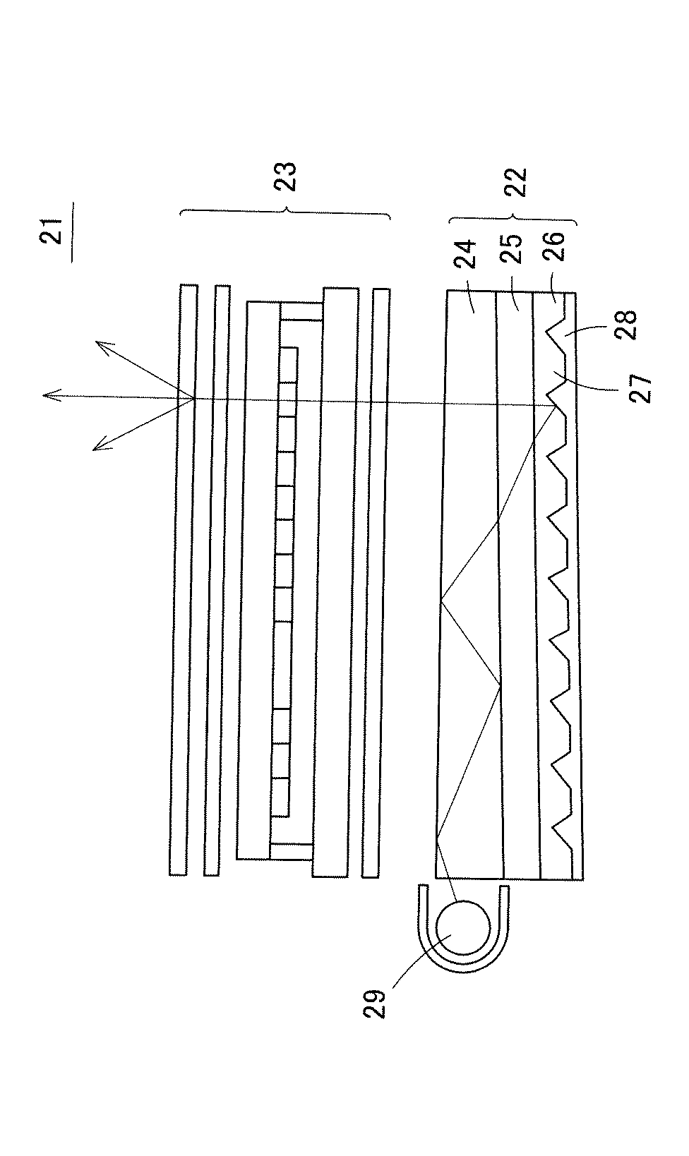
図6は、特許文献2に開示された液晶表示装置の構造を示す概略図である。この液晶表示装置21は、面光源装置22の全面に液晶表示パネル23を重ねたものである。面光源装置22は楔形をした導光板24を備え、導光板24の下面に導光板24よりも低屈折率の第1光透過層25を重ね、第1光透過層25の下面に導光板24とほぼ同じ屈折率の光偏向層26を重ねている。光偏向層26は、導光板24とほぼ同じ屈折率を有する第2光透過層27の裏面に金属材料からなるマイクロミラー28を一体に形成したものである。また、導光板24の厚みの大きな側の端面に対向させて冷陰極型蛍光灯のような光源29を配置している。
FIG. 6 is a schematic diagram showing the structure of the liquid crystal display device disclosed in
図6において光路を矢印で示すように、この面光源装置22においては、光源29から放射された光は、導光板24の側面を通過して導光板24内に入る。導光板24内に入った光は、導光板24の上面と下面との間で全反射を繰り返しながら導光板24内を導光する。導光板24内の光は、楔形をした導光板24の上面と下面とで全反射する都度、導光板24の下面に入射する際の入射角(光線が導光板24の下面に立てた法線となす角度)が小さくなる。そして、導光板24の下面に入射する光の入射角が第1光透過層25と導光板24の界面における全反射の臨界角よりも小さくなると、その光は導光板24の下面を透過して第1光透過層25に入射し、さらに第2光透過層27内に入射してマイクロミラー28で反射され、マイクロミラー28で反射された光は第2光透過層27、第1光透過層25及び導光板24を透過して導光板24の上面(光出射面)から出射される。
In this surface
このような構造の面光源装置22では、導光板24内を導光する光のうち、導光板24の下面に入射する際の入射角が全反射の臨界角よりも小さくなった狭い範囲の光だけが第1及び第2光透過層25、27を透過してマイクロミラー28で反射されるため、面光源装置22から狭い指向特性の光を出射させることができる。
In the surface
しかし、この面光源装置22でも、導光板24の下面には導光板24よりも低屈折率の第1光透過層25が空気層を介することなく密着しているので、図5(b)で斜線を施した範囲に相当する光は、図7に示すように最初に導光板24の下面に入射したときに第1及び第2光透過層25、27を透過してマイクロミラー28で反射され、一度に面光源装置22の正面から出射されてしまう。そのため、この面光源装置22を用いた場合でも、光源29の近傍が明るく光って輝度ムラが生じ、表示面全体を均一に発光させることができなかった。また、光源29の近傍で光が漏れて光の利用効率が低下するため、表示面が暗くなる問題があった。
However, also in this surface
本発明は、このような技術的課題に鑑みてなされたものであって、その目的とするところは、光源の近傍における光の漏れを低減してより均一に発光させることができ、さらに狭い指向特性の光を出射させることで発光輝度を向上させることのできる面光源装置を提供するにある。また、本発明の別な目的は、当該面光源装置を用いた液晶表示装置を提供することにある。 The present invention has been made in view of such a technical problem, and an object of the present invention is to reduce light leakage in the vicinity of the light source and to emit light more uniformly, and to further narrow the direction. An object of the present invention is to provide a surface light source device capable of improving the light emission luminance by emitting characteristic light. Another object of the present invention is to provide a liquid crystal display device using the surface light source device.
本発明の第1の面光源装置は、光源と、前記光源と対向する位置に設けられていて前記光源の光を光入射端面から導入して光出射面から外部へ出射させる導光板とを備えた面光源装置であって、前記導光板の端縁に沿って複数個の前記光源が配置され、前記導光板は、透光性材料からなる導光基板と、前記導光基板の前記光出射面と反対側の面に密着した、前記導光基板よりも低屈折率の低屈折率層と、前記低屈折率層の前記光出射面と反対側の面に密着した反射層とを備え、前記導光基板は、前記光源と対向する位置に設けられた光導入部と、前記光導入部から導光された光を外部へ出射する前記光出射面を備えた導光板本体とを一体として構成され、前記光導入部の光出射側の面又はその反対側の面における前記光出射面と平行な領域には、前記光源に近い側から前記光源より遠ざかる方向へ向けて延びた複数のパターンによって、前記光入射端面から前記光導入部に入射した光を前記導光基板内に閉じ込めるための指向性変換部が設けられ、前記導光板本体の前記光出射面側には、導光板本体内の光を反射させて導光板本体の前記光出射面と反対側の面から前記低屈折率層へ漏れさせるための光制御パターンが形成され、前記低屈折率層と前記反射層との界面又は前記反射層の前記界面と反対側の面には、前記低屈折率層へ漏れた光を反射させて前記光出射面から出射させるための光出射手段が形成され、前記導光板の光出射面に垂直な方向から見て、いずれか任意の光源の中心を通り前記導光板の端縁に垂直な方向にX軸を定め、前記導光板の端縁に沿ってY軸を定めたとき、当該光源に対応する指向性変換部は、
X>0
X≦{−2Y+(2P−W)}/(2tanα)
X≦{2Y+(2P−W)}/(2tanα)
(ただし、P:前記光源間の距離
W:前記光源の光出射窓の幅
α:導光板の屈折率をngとするとき、α=arcsin(1/ng)で表される角度)
の3式を同時に満たす領域の内部に位置していることを特徴としている。
The first surface light source device of the present invention includes a light source and a light guide plate that is provided at a position facing the light source and introduces light from the light source from a light incident end surface and emits the light from the light emitting surface to the outside. A plurality of light sources disposed along an edge of the light guide plate, the light guide plate comprising a light guide substrate made of a light-transmitting material, and the light emission of the light guide substrate. A low refractive index layer having a lower refractive index than that of the light guide substrate, which is in close contact with the surface opposite to the surface, and a reflective layer in close contact with the surface opposite to the light exit surface of the low refractive index layer, The light guide substrate integrally includes a light introducing portion provided at a position facing the light source, and a light guide plate body including the light emitting surface that emits light guided from the light introducing portion to the outside. It is configured, in the region parallel with the light emitting surface in the surface or the opposite surface thereof on the light emission side of the light introducing section , A plurality of patterns extending toward a direction away from the light source from the side close to the light source, the directivity converting portion for confining light incident on the light introducing portion from the light incident end face to the light guide substrate Provided on the light exit surface side of the light guide plate body for reflecting light in the light guide plate body to leak from the surface opposite to the light exit surface of the light guide plate body to the low refractive index layer A light control pattern is formed, and light emitted from the low refractive index layer is reflected on the interface between the low refractive index layer and the reflective layer or on the surface opposite to the interface of the reflective layer to emit the light. A light emitting means for emitting light from the surface is formed, and when viewed from a direction perpendicular to the light emitting surface of the light guide plate, it passes through the center of any light source and extends in the direction perpendicular to the edge of the light guide plate. And the Y-axis is defined along the edge of the light guide plate , Directivity converting unit corresponding to the light source,
X> 0
X ≦ {−2Y + (2P−W)} / (2 tan α)
X ≦ {2Y + (2P−W)} / (2tanα)
(Where P: distance between the light sources
W: width of the light exit window of the light source
α: α = arcsin (1 / ng), where ng is the refractive index of the light guide plate)
It is characterized in that it is located within a region that simultaneously satisfies the above three formulas .
本発明の第1の面光源装置においては、指向性変換部によって導光板本体内を導光する光の指向特性を狭くすることができ、光源の近傍における光の漏れを防ぐことができる。その結果、発光面における輝度分布の均一性を向上させることができ、また光の利用効率が向上することで発光面の輝度が向上する。また、指向性変換部で指向特性を狭くした光の一部を低屈折率層へ透過させることで光出射面から出射される光の指向特性をより狭くすることができ、面光源装置の正面輝度を向上させることができる。また、指向性変換部によって導光板本体内の光の指向性を狭くすることにより、光制御パターンや光出射手段による光の制御性も高くなる。よって、この面光源装置によれば、狭指向性で、輝度が高く、均一発光が可能なバックライトを実現することができる。
また、本発明の第1の面光源装置にあっては、光導入部の光出射面側の面またはその反対面における前記光出射面と平行な領域においては、光源に近い側から光源より遠ざかる方向へ向けて延びた複数のパターンによって指向性変換部を構成しているので、指向性変換部によって光入射端面から光導入部に入射した光を導光基板内に閉じ込めることができる。
さらに、本発明の第1の面光源装置にあっては、導光板の光出射面に垂直な方向から見て、いずれか任意の光源の中心を通り導光板の端縁に垂直な方向にX軸を定め、導光板の端縁に沿ってY軸を定めたとき、当該光源に対応する指向性変換部が、
X>0
X≦{−2Y+(2P−W)}/(2tanα)
X≦{2Y+(2P−W)}/(2tanα)
の3式を同時に満たす領域の内部に位置しているので、それぞれの指向性変換部に、対応しない他の光源からの光が入射して反射又は透過するのを避けることができ、指向性変換部や光導入部からの光の漏れを低減することができる。
In the 1st surface light source device of this invention, the directivity characteristic of the light which guides the inside of a light-guide plate main body by a directivity conversion part can be narrowed, and the leak of the light in the vicinity of a light source can be prevented. As a result, the uniformity of the luminance distribution on the light emitting surface can be improved, and the luminance of the light emitting surface is improved by improving the light utilization efficiency. In addition, by transmitting a part of the light whose directivity is narrowed by the directivity converter to the low refractive index layer, the directivity of the light emitted from the light exit surface can be further narrowed. Brightness can be improved. Further, by narrowing the directivity of the light in the light guide plate body by the directivity conversion section, the light controllability by the light control pattern and the light emitting means is also enhanced. Therefore, according to this surface light source device, it is possible to realize a backlight having narrow directivity, high luminance, and uniform light emission.
In the first surface light source device of the present invention, in the region parallel to the light emitting surface on the light emitting surface side of the light introducing portion or the opposite surface, the light introducing portion is moved away from the light source from the side close to the light source. Since the directivity converting unit is configured by a plurality of patterns extending in the direction, the light incident on the light introducing unit from the light incident end surface can be confined in the light guide substrate by the directivity converting unit.
Furthermore, in the first surface light source device of the present invention, when viewed from the direction perpendicular to the light exit surface of the light guide plate, it passes through the center of any light source and extends in the direction perpendicular to the edge of the light guide plate. When the axis is defined and the Y axis is defined along the edge of the light guide plate, the directivity conversion unit corresponding to the light source is
X> 0
X ≦ {−2Y + (2P−W)} / (2 tan α)
X ≦ {2Y + (2P−W)} / (2tanα)
Therefore, it is possible to avoid reflection or transmission of light from other light sources that do not correspond to each directivity conversion unit, and directivity conversion. Leakage of light from the light source and the light introduction part can be reduced.
本発明の第2の面光源装置は、光源と、前記光源と対向する位置に設けられていて前記光源の光を光入射端面から導入して光出射面から外部へ出射させる導光板とを備えた面光源装置であって、前記導光板の端縁に沿って複数個の前記光源が配置され、前記導光板は、透光性材料からなる導光基板と、前記導光基板の前記光出射面と反対側の面に密着した、前記導光基板よりも低屈折率の低屈折率層と、前記低屈折率層の前記光出射面と反対側の面に密着した、前記低屈折率層よりも高屈折率の高屈折率層と、前記高屈折率層の前記光出射面と反対側の面に密着した反射層とを備え、前記導光基板は、前記光源と対向する位置に設けられた光導入部と、前記光導入部から導光された光を外部へ出射する前記光出射面を備えた導光板本体とを一体として構成され、前記光導入部の光出射側の面又はその反対側の面における前記光出射面と平行な領域には、前記光源に近い側から前記光源より遠ざかる方向へ向けて延びた複数のパターンによって、前記光入射端面から前記光導入部に入射した光を前記導光基板内に閉じ込めるための指向性変換部が設けられ、前記導光板本体の前記光出射面側には、導光板本体内の光を反射させて導光板本体の前記光出射面と反対側の面から前記低屈折率層側へ漏れさせるための光制御パターンが形成され、前記高屈折率層と前記反射層との界面又は前記反射層の前記界面と反対側の面には、前記高屈折率層へ漏れた光を反射させて前記光出射面から出射させるための光出射手段が形成され、前記導光板の光出射面に垂直な方向から見て、いずれか任意の光源の中心を通り前記導光板の端縁に垂直な方向にX軸を定め、前記導光板の端縁に沿ってY軸を定めたとき、当該光源に対応する指向性変換部は、
X>0
X≦{−2Y+(2P−W)}/(2tanα)
X≦{2Y+(2P−W)}/(2tanα)
(ただし、P:前記光源間の距離
W:前記光源の光出射窓の幅
α:導光板の屈折率をngとするとき、α=arcsin(1/ng)で表される角度)
の3式を同時に満たす領域の内部に位置していることを特徴としている。
A second surface light source device of the present invention includes a light source and a light guide plate that is provided at a position facing the light source and introduces light from the light source from a light incident end surface and emits the light from a light emitting surface to the outside. A plurality of light sources disposed along an edge of the light guide plate, the light guide plate comprising a light guide substrate made of a light-transmitting material, and the light emission of the light guide substrate. A low refractive index layer having a lower refractive index than that of the light guide substrate, which is in close contact with the surface opposite to the surface, and the low refractive index layer in close contact with the surface of the low refractive index layer opposite to the light emitting surface. A high refractive index layer having a higher refractive index and a reflective layer in close contact with the surface opposite to the light exit surface of the high refractive index layer, and the light guide substrate is provided at a position facing the light source. And the light guide plate body provided with the light emitting surface for emitting the light guided from the light introducing portion to the outside. As configured, the parallel area and the light emitting surface in the surface or the opposite surface thereof on the light emission side of the light introducing section, from the side close to the light source of the plurality extending toward a direction away from the light source A directivity conversion unit for confining the light incident on the light introduction unit from the light incident end surface in the light guide substrate is provided by a pattern, and the light guide plate body is disposed on the light exit surface side of the light guide plate body. A light control pattern is formed to reflect the light inside the light guide plate body and leak from the surface opposite to the light exit surface of the light guide plate body to the low refractive index layer side, and between the high refractive index layer and the reflective layer A light emitting means for reflecting the light leaked to the high refractive index layer and emitting it from the light emitting surface is formed on the interface or the surface opposite to the interface of the reflective layer, and the light of the light guide plate Any one as seen from the direction perpendicular to the exit surface Defining a X-axis in a direction perpendicular to the center of the light source to the edge of the street the light guide plate, when defining the Y-axis along the edge of the light guide plate, the directivity converting unit corresponding to the light source,
X> 0
X ≦ {−2Y + (2P−W)} / (2 tan α)
X ≦ {2Y + (2P−W)} / (2tanα)
(Where P: distance between the light sources
W: width of the light exit window of the light source
α: α = arcsin (1 / ng), where ng is the refractive index of the light guide plate)
It is characterized in that it is located within a region that simultaneously satisfies the above three formulas .
本発明の第2の面光源装置にあっても、第1の面光源装置と同様な作用効果を奏する。さらに、第2の面光源装置では、低屈折率層の光が高屈折率層へ入ることによってさらに狭指向性の光となる。そして、高屈折率層で指向特性が狭くなった光が光出射手段で反射されて光出射面から出射される。この結果、第2の面光源装置によれば、さらに出射光を狭指向性にすることができ、正面輝度を向上させることができる。
また、本発明の第2の面光源装置にあっては、光導入部の光出射面側の面またはその反対面における前記光出射面と平行な領域においては、光源に近い側から光源より遠ざかる方向へ向けて延びた複数のパターンによって指向性変換部を構成しているので、指向性変換部によって光入射端面から光導入部に入射した光を導光基板内に閉じ込めることができる。
さらに、本発明の第2の面光源装置にあっては、導光板の光出射面に垂直な方向から見て、いずれか任意の光源の中心を通り導光板の端縁に垂直な方向にX軸を定め、導光板の端縁に沿ってY軸を定めたとき、当該光源に対応する指向性変換部が、
X>0
X≦{−2Y+(2P−W)}/(2tanα)
X≦{2Y+(2P−W)}/(2tanα)
の3式を同時に満たす領域の内部に位置しているので、それぞれの指向性変換部に、対応しない他の光源からの光が入射して反射又は透過するのを避けることができ、指向性変換部や光導入部からの光の漏れを低減することができる。
Even in the second surface light source device of the present invention, the same operational effects as the first surface light source device can be obtained. Further, in the second surface light source device, the light of the low refractive index layer enters the high refractive index layer, and becomes light with a narrower directivity. Then, the light whose directivity characteristics are narrowed by the high refractive index layer is reflected by the light emitting means and emitted from the light emitting surface. As a result, according to the second surface light source device, the emitted light can be made more narrow and directivity can be improved.
Further, in the second surface light source device of the present invention, in the surface parallel to the light emitting surface on the light emitting surface side of the light introducing portion or the opposite surface, the light introducing portion is moved away from the light source from the side close to the light source. Since the directivity converting unit is configured by a plurality of patterns extending in the direction, the light incident on the light introducing unit from the light incident end surface can be confined in the light guide substrate by the directivity converting unit.
Furthermore, in the second surface light source device of the present invention, when viewed from the direction perpendicular to the light exit surface of the light guide plate, it passes through the center of any light source and extends in the direction perpendicular to the edge of the light guide plate. When the axis is defined and the Y axis is defined along the edge of the light guide plate, the directivity conversion unit corresponding to the light source is
X> 0
X ≦ {−2Y + (2P−W)} / (2 tan α)
X ≦ {2Y + (2P−W)} / (2tanα)
Therefore, it is possible to avoid reflection or transmission of light from other light sources that do not correspond to each directivity conversion unit, and directivity conversion. Leakage of light from the light source and the light introduction part can be reduced.
本発明に係る液晶表示装置は、本発明の面光源装置と、液晶パネルと、少なくとも前記面光源装置の前記導光板本体と前記液晶パネルとの間に介在して前記導光板本体を前記液晶パネルに密着させる少なくとも1層の接続層とからなる液晶表示装置において、前記各接続層のいずれかの屈折率が、前記導光板本体の屈折率よりも低いことを特徴としている。かかる液晶表示装置においては、面光源装置を低屈折率の接続層によって液晶パネルに取り付けているので、薄い面光源装置の場合でも、面光源装置の反りなどを防ぐことができる。しかも、面光源装置として本発明の面光源装置を用いることにより、直接接続層へ光が漏れるのを防止することができ、液晶表示装置の表示面を高輝度化し、輝度分布を均一化できる。 The liquid crystal display device according to the present invention includes the surface light source device of the present invention, a liquid crystal panel, and at least the light guide plate body of the surface light source device and the liquid crystal panel interposed between the light guide plate body and the liquid crystal panel. A liquid crystal display device comprising at least one connection layer in close contact with each other is characterized in that the refractive index of any one of the connection layers is lower than the refractive index of the light guide plate body. In such a liquid crystal display device, since the surface light source device is attached to the liquid crystal panel by a connection layer having a low refractive index, the surface light source device can be prevented from warping even in the case of a thin surface light source device. In addition, by using the surface light source device of the present invention as the surface light source device, it is possible to prevent light from leaking directly to the connection layer, and to increase the luminance of the display surface of the liquid crystal display device and make the luminance distribution uniform.
なお、本発明における前記課題を解決するための手段は、以上説明した構成要素を適宜組み合せた特徴を有するものであり、本発明はかかる構成要素の組合せによる多くのバリエーションを可能とするものである。 The means for solving the above-described problems in the present invention has a feature in which the above-described constituent elements are appropriately combined, and the present invention enables many variations by combining such constituent elements. .
以下、添付図面を参照しながら本発明の好適な実施形態を説明する。 Hereinafter, preferred embodiments of the present invention will be described with reference to the accompanying drawings.
(第1の実施形態)
以下、図8〜図10を参照して本発明の実施形態1による面光源装置31の構造を説明する。図8(a)及び(b)は、それぞれ面光源装置31の表面側と裏面側の構造を示す斜視図である。図9(a)は、面光源装置31の一部破断した平面図である。図9(b)は、面光源装置31の中心を通る断面を示す図である。
(First embodiment)
Hereinafter, the structure of the surface
面光源装置31は、点光源32と導光板33とからなる。点光源32は、1個又は近接した複数個のLEDを内蔵したものであって、白色発光するものである。点光源32は、例えば図9(b)に示すように、1個又は複数個のLED34を透明封止樹脂35内に封止し、さらに当該透明封止樹脂35の正面を除く各面を白色樹脂36で覆ったものである。透明封止樹脂35の正面が、白色樹脂36から露出していて光出射窓37となっている。そして、LED34から出射した光は、直接に光出射窓37から出射され、あるいは透明封止樹脂35と白色樹脂36との界面で反射された後に光出射窓37から出射される。
The surface
点光源32は図9(b)に示したようなものに限らない。ここでいう点光源32は、厳密な意味での点光源ではなく、冷陰極管が線状光源と呼ばれるのに対して点光源と称するものである。すなわち、点光源とは、導光板33の幅に比べて小さな光源ということであり、点光源32も有限の幅を持つが、冷陰極管のように10mm以上の長さもしくは幅を持つようなものではない。
The point
例えば、別な点光源32としては、サイドビュー型のLEDなどがある。サイドビュー型のLEDでは、1パッケージ内に1つ以上のLEDチップが入っており、複数個のLEDチップが同時に封止されていてもよい。複数個のLEDチップが同時に封止されたものでは、出射窓の幅が5mm程度になるものがあるが、導光板の発光領域の幅が2インチ程度であるのと比べれば十分に小さいので、点光源とみなすことができる。また、光ファイバを用いて導いた光を導光板に導入するようにしてもよい。その場合には、光ファイバの光出射端面を点光源とみなすことができる。
For example, as another point
導光板33は、透光性材料からなる導光基板38の下面に、導光基板38よりも屈折率の小さな透光性材料からなる低屈折率層39を設け、低屈折率層39の下面に金属薄膜等によって反射層40を形成したものである。導光基板38は、表面と裏面が平行なプレート状に成形されており、概念上は導光板本体41と光導入部42に分けることができる。光導入部42は、導光板本体41の光源側端部に設けられており、光導入部42と導光板本体41は一体に、かつ、連続的に成形されている。導光基板38は、ポリカーボネイト樹脂(PC)、アクリル樹脂、シクロオレフィン系材料、ポリメチルメタクリレート(PMMA)などの高屈折率の透明樹脂や高屈折率のガラスによって成形されており、その屈折率は1.5〜1.6であることが好ましい。また、導光基板38の厚みは、0.3mm〜0.5mm程度であることが望ましい。光導入部42の端面(光入射端面43)の厚みは、点光源32の光出射窓37の高さよりも厚くしておけば、点光源32から出射された光を光入射端面43から光導入部42内に効率よく入射させることができ、面光源装置31の光利用効率が高くなる。しかし、導光基板38はできるだけ薄くすることが望まれるので、光導入部42の端面の厚みは、点光源32の光出射窓37の高さと等しいことが好ましい。
The
光導入部42においては、導光板本体41の光出射面44と同じ側の面(表面)に指向性変換部45が形成されている。指向性変換部45は、光導入部42内において、導光板本体41と隣接する領域に形成されている。言い換えると、導光板33の光出射面44に垂直な方向から見て、指向性変換部45の点光源32から遠い側に位置する縁から光入射端面43までの領域を光導入部42と呼び、それ以外の領域(指向性変換部45の点光源32から遠い側に位置する縁から導光板33の光入射端面43と反対側の端面までの領域)を導光板本体41と呼ぶ。光導入部42の裏面は平滑に形成されている。指向性変換部45は、光入射端面43から入射した光の指向特性を変化させて導光基板38内に閉じ込める働きをするものであるが、その詳細については後述する。
In the
導光板本体41の光出射面44には、光源側から導光してくる光を全反射させて光の導光方向を変化させるための微細な拡散パターン46(光制御パターン)が多数凹設されている。拡散パターン46は、図8(a)では規則的に配置しているが、ランダムに配置されていてもよい。あるいは、光出射面44の面内で輝度の均一性が得られるように拡散パターン46を千鳥配置したり、拡散パターン46を放射状に(同心円状に)配列したりするなど、一般的な配置方法を用いてもよい。また、点光源32から遠くなるに従って到達する光量が少なくなるので、面光源装置31の発光輝度を均一化するためには、点光源32から遠くなるに従って拡散パターン46の分布密度又は数密度が大きくなるようにすることが望ましい。図10(a)、(b)、(c)及び(d)は、拡散パターン46の形状を示す斜視図、平面図、(光源側から見た)正面図及び側面図である。この拡散パターン46は、4面の傾斜面からなるダイア形状の凹部となっている。
A large number of fine diffusion patterns 46 (light control patterns) are provided in the
導光板本体41の裏面は、平滑となっていて光出射面44と平行に形成されている。導光板本体41の裏面には、空気層を挟むことなく導光板本体41の裏面に密着させるようにして、導光板本体41よりも低屈折率の透明樹脂等からなる低屈折率層39が形成されている。低屈折率層39は、ポリメチルメタクリレート(PMMA)、ポリカーボネイト樹脂(PC)、アクリル樹脂、シクロオレフィン系材料などの透明樹脂やガラスによって成形されている。また、低屈折率層39は導光板本体41よりも低屈折率で、かつ、比較的高屈折率であることが望ましいので、屈折率が1.4以上1.5未満の材料が好ましい。具体例としては、ポリカーボネイト樹脂からなる導光基板38の下面にポリメチルメタクリレートからなる低屈折率層39を形成したものがある。低屈折率層39の厚みは、5μm程度である。低屈折率層39の下面には、斜め方向から低屈折率層39の下面に入射した光を反射させて光出射面44にほぼ垂直な方向へ出射させるための微細な偏向パターン47(光出射手段)が形成されている。偏向パターン47は、断面三角形状(プリズム状)の凸部となっていて導光基板38の幅方向に長く伸びており、光入射端面43に垂直な方向に配列されている。図8や図9では偏向パターン47を隙間無く配列しているが、間隔をあけて離散的に配置してもよい。その場合、偏向パターン47は凹状となっていてもよく、凸状となっていてもよく、凹状と凸状の組合せであってもよい。また、偏向パターン47は、平面で構成されていても、曲面で構成されていてもよい。
The back surface of the light
さらに、この偏向パターン47を覆うようにして、低屈折率層39の下面全面にはAgやAl等の金属蒸着膜や白色樹脂被膜からなる反射層40が形成され、低屈折率層39と反射層40によって裏面鏡が構成されている。
Further, a
(作用効果)
まず、図11、図12を参照しながら、上記のような構造を有する面光源装置31における光の挙動とその作用効果を説明する。これらの光の挙動を実現し、その作用効果を奏するための具体的な構成や条件などについては、その後に詳述する。なお、以下においては、導光基板38の光入射端面43に垂直な方向をX方向とし、光出射面44に垂直な方向をZ方向とし、X方向及びZ方向に直交する方向をY方向とする。
(Function and effect)
First, with reference to FIG. 11 and FIG. 12, the behavior of light and its effects in the surface
図11は、面光源装置31における光の挙動を示す図である。また、図12は、導光板33内における光の指向特性の変化を説明する図である。図12に示す指向特性P1は、点光源32の光が光導入部42に入射した直後の指向特性を表している。導光基板38の屈折率をngとすれば、光導入部42に入射した直後の光の指向性広がりは、
±α=±arcsin(1/ng) …(数式1)
で表されるから、ng=1.59とすると、指向特性P1の指向性広がりは±α=±39.0°となる。
FIG. 11 is a diagram illustrating the behavior of light in the surface
± α = ± arcsin (1 / ng) (Formula 1)
Therefore, when ng = 1.59, the directivity spread of the directivity characteristic P1 is ± α = ± 39.0 °.
導光基板38の屈折率ngを1.59とすると、平坦面49又はその裏面と空気層との界面における全反射の臨界角は、同じく39.0°であるから、これを水平方向(X軸方向)から測った角度に換算すると、51.0°となる。すなわち、水平方向から測って51.0°以上の角度の光と、−51.0°以下の角度の光は光導入部42と空気層の界面から漏れる。しかし、光導入部42に入射した光の指向性広がりは、±39.0°であるから、光導入部42に入射した光は空気との界面では漏れることが無く、全反射しながら導光板33内を導光される。
If the refractive index ng of the
指向特性P1のうち斜線を施した領域の光は、指向性変換部45がない場合には、図11に破線矢印で示した光L3のように導光板本体41と低屈折率層39の界面に達したときに直ちに低屈折率層39側へ漏れ、反射層40で反射され光出射面44から出射される。一方、指向特性P1のうち斜線領域外の光は、低屈折率層39との界面で全反射される光である。すなわち、指向特性P1の斜線領域の光は、図5(b)の斜線領域内の光に相当する。図11に示す光線L1、L2はいずれも、図12の指向特性P1において斜線を施した領域内の光を表しており、指向性変換部45がなければ破線矢印の光L3のように光出射面44の点光源近傍を光らせて輝度ムラを発生させる原因となる。
The light in the shaded region of the directivity characteristic P1 is the interface between the light
導光基板38の屈折率をng、低屈折率層39の屈折率をn1とすれば、導光板本体41と低屈折率層39との界面における全反射の臨界角γは、
γ=arcsin(n1/ng) …(数式2)
であり、これは水平方向から測った角度βに換算すれば、
β=90°−γ=90°−arcsin(n1/ng) …(数式3)
となる。いま、ng=1.59、n1=1.4とすれば、β=28.3°となる。
If the refractive index of the
γ = arcsin (n1 / ng) (Formula 2)
This is the angle β measured from the horizontal direction,
β = 90 ° -γ = 90 ° -arcsin (n1 / ng) (Formula 3)
It becomes. If ng = 1.59 and n1 = 1.4, β = 28.3 °.
従って、光導入部42に入射した指向性広がり±α(=±39.0°)の光のうち、−β〜+βの範囲の光(斜線領域外の光)は、光導入部42と空気との界面でも導光板本体41と低屈折率層39との界面でも全反射し、導光基板38から漏れることなく導光される。これに対し、−α〜−βの範囲の光L2と+β〜+αの範囲の光L1(斜線領域の光)は、指向性変換部45がない場合には、空気との界面では全反射されるが、低屈折率層39との界面を透過して光出射面44から漏れる。
Therefore, among the light having the directivity spread ± α (= ± 39.0 °) incident on the
面光源装置31では、これらの光L1、L2を指向性変換部45で反射させることによって指向特性を変換し、導光板本体41内に閉じ込める働きをする。指向特性で説明すると、光導入部42内に入った直後の指向特性P1は、光が指向性変換部45で反射されることによって光出射面44に垂直な断面内における広がりが狭められる。すなわち、指向性変換部45で狭められた指向特性P2を持つ光の指向性広がりγは、指向特性P1における斜線領域外の光の指向性広がりβ程度に小さくなっている(好ましくは、γ≦βである。)。指向特性P2が指向特性P1の斜線領域外の狭い指向特性となった場合には、指向性変換部45で反射された後の光(指向特性P2)は、導光板本体41と低屈折率層39との界面で全反射され、図11に示した光L1のように、拡散パターン46で反射されない限り、導光板本体41の表面(光出射面44)と裏面(低屈折率層39との界面)で全反射を繰り返しながら導光板本体41内を導光する。
In the surface
こうして導光板本体41内に閉じ込められた光が拡散パターン46で全反射されると、その光は下方へ向いて進むので、指向特性P2の向きが変化して指向特性P3となる。指向特性P3における斜線領域外の光は、低屈折率層39との界面における全反射の臨界角よりも入射角が大きな光を表している。指向特性P3の光のうち斜線領域外の光は低屈折率層39との界面で全反射するが、斜線領域内の光は図11の光L2のように低屈折率層39に入射する。よって、低屈折率層39に入射した光の指向特性はP4のように狭くなる。この指向特性の狭い光は、図11の光L2のように、反射層40で反射されて光出射面44へ向かい(指向特性P5)、さらに光出射面44から外部へ出射される(指向特性P6)。
Thus, when the light confined in the light
この結果、この面光源装置31によれば、指向性変換部45を設けることによって導光板本体41内を導光する光を精度よく制御することが可能になり、点光源32の近傍において指向特性P1の斜線領域内の光が光出射面44から漏れて輝度ムラを発生させるのを防止することができる。例えば、導光基板38の屈折率を1.59とし、低屈折率層39の屈折率を1.4とした場合、導光板33に指向性変換部45が設けられていなければ、面光源装置の中心線A−A(図9参照)に沿った光出射面44の輝度分布は図13に細実線で示すようになり、点光源32の近傍が明るく光って面光源装置31に顕著な輝度ムラを生じる。これに対し、指向性変換部45で反射後の指向特性(P2)では指向性広がりγが28°程度まで狭められたとすると、面光源装置の中心線A−Aに沿った光出射面の輝度分布は図13に太実線で示すようになり、光出射面44の輝度が均一化される。さらに、図13に示されているように、点光源32の近傍からの光の漏れを抑制することにより、光出射面44全体で輝度が向上する。
As a result, according to the surface
また、導光板本体41の下面に低屈折率層39と反射層40を設けているので、指向性変換部45で反射されることによって指向特性が狭くなった光の一部が導光板本体41と低屈折率層39の界面を通過することによりさらに指向特性が狭くなる。その結果、光出射面44から出射される光の指向特性が狭くなり、面光源装置31の正面輝度が向上する。図14は光出射面44から出射された光の指向特性(Z方向から見た指向特性)を示すが、X方向において非常に狭い指向特性を実現できることが分かる。また、図15は、この指向特性をZX面内の各出射方向における輝度分布として示した図である。図15によれば、±20°以内に全出射光の90%以上の光量が集まっていることが分かる。なお、図14及び図15は、拡散パターン46の傾斜角εを9.3°とし、偏向パターン47の頂角κを120°とした場合の特性である。
Further, since the low
したがって、この面光源装置31によれば、指向性変換部45によって導光板本体41内を導光する光の指向特性を狭くすることができ、点光源の近傍における光の漏れを防ぐことができる。その結果、発光面における輝度分布の均一性を向上させることができ、また光の利用効率が向上することで発光面の輝度が向上する。また、指向性変換部45で指向特性を狭くした光の一部を低屈折率層39へ透過させることで光出射面44から出射される光の指向特性をより狭くすることができ、面光源装置31の正面輝度を向上させることができる。また、指向性変換部45によって導光板本体41内の光の指向性を狭くすることにより、拡散パターン46や偏向パターン47による光の制御性も高くなる。よって、この面光源装置31によれば、狭指向性で、輝度が高く、均一発光が可能なバックライトを実現することができる。さらに、プリズムシートなどの付加的なシートが必要ないので、面光源装置31もしくは液晶表示装置を薄型化できる。
Therefore, according to the surface
(指向性変換部について)
つぎに、上記のような光の挙動と作用効果を実現するための詳細を説明する。まず、指向性変換部45の構造を説明する。
(Directivity conversion unit)
Next, details for realizing the above-described behavior and effects of light will be described. First, the structure of the
図8に示すように、指向性変換部45は、矩形領域又は帯状領域に設けられており、V溝状をした同一形状の指向性変換パターン48を放射状に並べて構成されている。図16(a)は、ある指向性変換パターン48の谷線に沿って断面した導光板33の一部を示す断面図である。図16(b)は、図9(a)のB−B線に沿った、各指向性変換パターン48の稜線48aに垂直な断面の一部を示す拡大図である。光導入部42のうち指向性変換部45よりも点光源32に近い領域は光出射面44と面一の平坦面となっており(この平坦な領域を光導入部42の平坦面49と呼ぶ。)、指向性変換部45は光出射面44及び平坦面49から引っ込むように形成されている。
As shown in FIG. 8, the
V溝状をした指向性変換パターン48の稜線48aは、光出射面44及び平坦面49を含む平面内にあって水平方向に延びている。また、指向性変換パターン48の谷線48bは、点光源32から遠い側で最も深く、点光源32に近い側で最も浅くなるように直線的に傾斜している。隣接する指向性変換パターン48間に形成されるV溝部の両端面はいずれも光出射面44及び平坦面49に垂直な面となっている。また、各指向性変換パターン48は同じ形状を有しており、点Sから等しい距離にある断面(稜線に垂直な断面)は互いに等しい断面形状となる。
The
各指向性変換パターン48の谷線48bを点光源32側へ向けて三次元的に延長した先は、ある1点もしくはある1点の近傍領域に集まっている。この実施形態の場合では、各指向性変換パターン48の谷線48bを延長した先は、平坦面49上において光導入部42の端面(光入射端面43)の中央部に位置する1点もしくはその近傍の1点もしくはそれらの1点の近傍領域に集まっている。この実施形態では、光導入部42の端面の中央部に位置する1点Sに集まっているものとする。同様に、各指向性変換パターン48の稜線48aを三次元的に延長した先も、ある1点もしくはある1点の近傍領域に集まっている。
The points where the
なお、指向性変換パターン48の谷線48bの傾斜角度(勾配)θは約1°であるが、この傾斜角度θの値は指向性変換パターン48の広がり(点Sを中心とするXY面内での広がり角)によって変化する。また、稜線48aに垂直な断面において稜線48aを挟む傾斜角のなす角度(山部の頂角)φは、107°<φ<154°とするのが好ましく、特に120°程度が好ましい。
The inclination angle (gradient) θ of the
指向性変換部45は、概略的にいえば、光を反射する前後で光の指向特性をX軸の回りに回転させ、あるいは傾ける働きをする。光導入部42に入射した光は、全体としては図18(a)に示すような円錐状の指向特性P1を有しているが、これをX軸方向のある点から見ると、図17(a)、(b)に示すようにY方向で狭い指向特性の光となる。この光が指向性変換部45で反射されると、その指向特性は図17(c)、(d)のように回転する。その結果、ZX面内ので指向性広がりはγに小さくなる。全体としては、図18(a)のような円錐状の指向特性P1は、図18(b)のようにZ方向で縮んだ扁平な指向特性P2に変換される。よって、γ≦βとなるように指向性変換部45の形状及び寸法が定められていれば、指向性変換部45で反射した光は、低屈折率層39との界面でも漏れなくなり、遠くまで光を運ぶことが可能になる。なお、指向性変換部45の詳細については、特願2008−180147又はPCT/JP2009/003184(参照文献1)や特願2007−155797又はPCT/JP2008/61610(参照文献2)を参照することができる。
Generally speaking, the
なお、図17(b)、(d)はZX面内から見た光の指向特性であって、このような指向特性はXY面内において斜め方向から点光源32を見た場合には、見る方向によって上下方向の指向性広がりは異なる。よって、指向性変換部45も正面方向と斜め方向とでパターンの形状を変化させることができるが、パターン製造の容易さから各方向の指向性変換パターン48を同じ形状のものとしている。
FIGS. 17B and 17D show the directivity characteristics of light viewed from within the ZX plane. Such directivity characteristics are seen when the point
また、光の漏れを完全に無くそうとすれば、指向性変換部45は、理論的には、−α〜−βの範囲の光と+β〜+αの範囲の光を全て指向性変換部45で受けることができるだけの長さ又は面積を有する必要があるが、その他の条件も考慮して、必ずしもこれらの範囲の光をすべて指向性変換部45で受ける必要はない。
If the light leakage is to be completely eliminated, the
図8、図9等に示した指向性変換部45は平坦面49や光出射面44から引っ込んでいたが、指向性変換部45は平坦面49や光出射面44から突出するように設けてもよい。図19は指向性変換部45を突出させた例を示す断面図である。この指向性変換部45は光導入部42の表面の一部を突出させるようにして形成されており、配列したV溝状の指向性変換パターン48の谷線48bは水平となっていて、光出射面44と同じ平面内にある。稜線48aの点光源32に近い側の端は高さが低く、稜線48aの点光源32から遠い側の端は高さが高くなっている。したがって、指向性変換部45のV溝は点光源32から離れるに従って直線的に深くなっており、稜線48aも直線状に傾斜している。また、指向性変換部45の両端面は、平坦面49及び光出射面44に対して垂直面となっている。それぞれの稜線48aを点光源32側へ延長した先は、1点Sに集まっている。
Although the
なお、指向性変換部45は、光出射面44よりも上に飛び出ている場合でも、光出射面44から下に引っ込んでいる場合でも、指向性変換部45と光出射面44との段差は小さいことが望ましい。
Note that the
また、指向性変換部45又は指向性変換パターン48は、ここに示した以外の形状を有するものであってもよい。例えば、参照文献1に開示したような種々の形状のものでもよい。また、それらの最適な設計例も参照文献1に記載したものを参照することができる。
Further, the
(拡散パターンについて)
つぎに、光出射面44に形成された拡散パターン46について説明する。拡散パターン46は、導光板本体41内に導光された光を全反射させることにより、導光板本体41の下面に対する入射角が小さくなるように光路を曲げる働きをする。図10に示した拡散パターン46はダイヤ形状に窪んでいたが、拡散パターン46が凹状である場合には点光源32に近い前半部で光を反射するので、点光源32から遠い側に位置する後半部の形状はどのようなものであっても特に問題はない。一方、拡散パターン46の前半部は、光を反射させて導光板本体41から低屈折率層39へ光を透過させる必要と、導光板本体41から低屈折率層39へ透過する光の指向性広がりができるだけ狭くなるようにする必要がある。そのためには、拡散パターン46のうち点光源32に近い側に位置する前半部の傾斜角εは、0°<ε≦20°とすることが好ましい。望ましくは、この傾斜角は0°<ε≦10°であり、さらに好ましくは0°<ε≦5°である。ただし、低屈折率層39に向かって抜ける光のピーク方向は、拡散パターン46の傾斜角εと、導光基板38の屈折率と低屈折率層39の屈折率の屈折率比との組合せによって制御することができるので、最適な傾斜角εの値は導光基板38と低屈折率層39の屈折率比を考慮して決めなければならない。
(Diffusion pattern)
Next, the
拡散パターン46は、前半部の傾斜角εが上記範囲にあればよいので、図10のように前半部と後半部とで対称である必要はなく、図20(a)に示す拡散パターン46のように前半部と後半部とで非対称となっていてもよい。特に、図20(a)のように断面が不等辺三角形状であってもよい。また、拡散パターン46は、図20(b)に示すように、光出射面44から突出していてもよい。凸状の拡散パターン46の場合には、導光板本体41へ導光してきた光は、拡散パターン46の後半部で全反射されるので、この場合には、後半部の傾斜角εが上記範囲にあればよい。さらに、拡散パターン46は、図20(c)に示すように、曲面で構成されていてもよい。図20(c)では、ドーム状をした拡散パターン46を光出射面44の表面に突出させている。
Since the
(偏向パターンについて)
図21は偏向パターン47における光の挙動を表した図である。偏向パターン47及び反射層40は、図21に光路を矢印で示すように、低屈折率層39へ入射した光を光出射面44に垂直な方向へ向けて反射させる働きをする。偏向パターン47は、断面三角形状をした棒状のパターンであって、低屈折率層39の下面に突出している。偏向パターン47は、その元になる金型を作り易いという理由から断面形状が二等辺三角形となっている。また、偏向パターン47の断面が二等辺三角形となっている場合には、点光源32と反対側にある斜面は、光源方向からの光(図21で実線矢印で示す光)を反射させて光出射面44から出射させる働きをする。図21の破線矢印は、導光基板38又は低屈折率層39の端面まで達し、その端面で反射されて戻ってきた光を表しており、光源側にある斜面は、この戻り光を反射させて光出射面44から出射させる働きをする。
(About deflection pattern)
FIG. 21 is a diagram showing the behavior of light in the
この偏向パターン47の頂角κは、107°以上136°以下であることが望ましい。この理由を図22に示す。図22は、偏向パターン47の頂角κの値に対する、指向特性で±20°の範囲内に含まれる光量の比率を表している。図22の横軸は、偏向パターン47の頂角κを表してる。また、図22の縦軸は、光出射面44から出射される光の指向特性において、光出射面44の法線に対して±90°以内の方向へ出射する光の全光量に対する±20°以内の方向へ出射する光の全光量の比率を百分率で表している。この光量の比率は60%以上であればよく、そのときの頂角κの値は、図22から107°以上136°以下であることが分かる。よって、偏向パターン47の頂角κは107°以上136°以下であることが望ましい。また、光出射面44から出射する光の指向特性におけるピーク方向は、偏向パターン47の傾斜面の傾斜角νによって制御することができる。
The apex angle κ of the
(第1の実施形態の変形例)
図23(a)〜(c)は、実施形態1の変形例を示す。図23(a)に示す変形例では、指向性変換部45を光導入部42の下面に形成している。この場合には、光が光導入部42の下面で反射する際に指向性変換部45で指向特性が変換される。なお、指向性変換部45が光導入部42の下面に設けられている場合には、指向性変換パターン48の谷線48bが稜線48aよりも光出射面44に近い側に位置する。
(Modification of the first embodiment)
FIGS. 23A to 23C show a modification of the first embodiment. In the modification shown in FIG. 23A, the
図23(b)に示す変形例では、指向性変換部45を光導入部42の下面に形成するとともに、低屈折率層39及び反射層40を光導入部42の端面まで延ばしている。低屈折率層39が光導入部42の端まで延びているため、指向性変換部45から低屈折率層39へ光は一部漏れるが、特許文献2のように指向性変換部45がない場合に比べれば効率は良くなり、さらに低屈折率層39が光導入部42の端面まで延びていることで作製がしやすくなる。従って、低屈折率層39及び反射層40を光導入部42の端まで延ばしていても差し支えない。ただし、点光源32の光が低屈折率層39の端面から低屈折率層39へ直接入射しないよう、点光源32の光出射窓37の下端は低屈折率層39の上面よりも上に位置させている。
In the modification shown in FIG. 23B, the
図23(c)に示す変形例では、指向性変換部45を光導入部42の上面に形成するとともに、低屈折率層39及び反射層40を光導入部42の端面まで延ばしている。このような形態では、光導入部42に入射した光の一部は指向性変換部45で変換されないで直接低屈折率層39に入射するが、低屈折率層39に入射した光は下方へ漏れることなく反射層40によって上方へ反射され、その後指向性変換部45へ入射する。
In the modification shown in FIG. 23C, the
図23(b)のような形態では、指向性変換部45が光導入部42と低屈折率層39の間に設けられていて光が漏れやすくなり、設計も困難になるので、低屈折率層39と反射層40を光導入部42の端まで延ばす場合には、図23(c)のように指向性変換部45が光導入部42と空気との界面に位置させることが望ましい。
In the form as shown in FIG. 23B, the
(第2の実施形態)
図24(a)は本発明の実施形態2による面光源装置51を示す概略断面図である。この面光源装置51では、実施形態1の面光源装置31において、低屈折率層39の下面と反射層40との間に、導光基板38の屈折率と同程度の屈折率を有する高屈折率層52を設けている。低屈折率層39は屈折率が1.4以上1.5未満の透明材料(例えば、ポリメチルメタクリレートなど)によって形成されており、均一な厚みを有していて5μm程度の厚みとなっている。高屈折率層52は、屈折率が1.5〜1.6程度の透明材料(例えば、屈折率が1.59のポリカーボネイト樹脂など)によって形成されており、10μm〜50μm程度の厚みを有している。偏向パターン47は高屈折率層52の下面に形成されており、高屈折率層52の表面に反射層40が設けられている。
(Second Embodiment)
FIG. 24A is a schematic cross-sectional view showing a surface
このような面光源装置51でも、実施形態1と同様な作用効果を奏することができる。また、実施形態2の面光源装置51では、低屈折率層39内に漏れた光を高屈折率層52内に入射させることで、低屈折率層39内の指向特性よりもさらに指向特性を狭くしたうえで反射層40により反射させることができる。その結果、高屈折率層52がない場合に比べて光出射面44から出射される光の指向特性を半値全幅で約10°狭くすることができる。さらに、下面に偏向パターン47と反射層40を形成された成形品の高屈折率層52を、導光基板38よりも低屈折率の透明樹脂接着剤を用いて導光基板38の下面に接着し、硬化した低屈折率透明接着剤によって低屈折率層39を形成することができるので、面光源装置51の製造が容易になる。
Even with such a surface
実施形態2においても、拡散パターン46は、図24(a)のようにダイヤ形状や三角形状のもの(コメットパターン)を光出射面44に凹設してもよく、図24(b)のようにダイヤ形状や三角形状のもの(コメットパターン)を光出射面44に突設してもよく、図24(c)のようにドーム状のもの(ブラストパターン)を光出射面44の上面に突設してもよい。また、低屈折率層39や高屈折率層52、反射層40を光導入部42の端面まで延ばしても差し支えない。
Also in the second embodiment, as the
図25は、図24(b)のように傾斜角ε=4°〜10°のコメットパターン状の拡散パターン46を突設し、偏向パターン47の頂角κ=120°とした面光源装置において、光出射面44から出射された光の指向特性(Z方向から見た指向特性)を示す図である。図25からは非常に狭い指向特性の得られることが分かる。また、図26は、図25のX方向における指向特性をZX面内の各出射方向における輝度分布として表し、図25のY方向における指向特性をZY面内の各出射方向における輝度分布として表した図である。図26によれば、ZX面内の指向特性では、光出射面44の法線方向から±20°以内に全出射光の98%の光量が集まっている。
FIG. 25 shows a surface light source device in which a comet pattern-
図27は、図24(c)のようにブラストパターン状の拡散パターン46を突設し、偏向パターン47の頂角κ=120°とした面光源装置において、光出射面44から出射された光の指向特性(Z方向から見た指向特性)を示す図である。図27からも非常に狭い指向特性の得られることが分かる。また、図28は、図27のX方向における指向特性をZX面内の各出射方向における輝度分布として表し、図27のY方向における指向特性をZY面内の各出射方向における輝度分布として表した図である。図28によれば、ZX面内の指向特性では、光出射面44の法線方向から±20°以内に全出射光の96%の光量が集まっている。
FIG. 27 shows the light emitted from the
よって、狭指向性のためには、ダイヤ形状などのコメットパターン状をした拡散パターン46の方が、ブラストパターン状の拡散パターン46よりも若干性能がよいことが分かる。
Therefore, it can be seen that, for narrow directivity, the performance of the
また、図29は、図24(c)のようにブラストパターン状の拡散パターン46を突設し、偏向パターン47の頂角κ=112°とした面光源装置において、光出射面44から出射された光の指向特性(Z方向から見た指向特性)を示す図である。また、図30は、図29のX方向における指向特性をZX面内の各出射方向における輝度分布として表し、図29のY方向における指向特性をZY面内の各出射方向における輝度分布として表した図である。
In addition, FIG. 29 is a surface light source device in which a blast pattern-
頂角κ=120°の場合の指向特性を示す図28では、ZX面内の指向特性のピーク方向がほぼ0°となっている。同様に、頂角κ=112°の場合の指向特性を示す図30でも、ZX面内の指向特性のピーク方向がほぼ0°となっている。ここに示していないシミュレーション結果も合わせて考えると、偏向パターン47の頂角κが110°以上120°以下の範囲にあれば、ZX面内の指向特性(X方向における指向特性)がほぼ0°の方向にピークを持つことが分かった。よって、偏向パターン47の頂角κを110°以上120°以下とすれば、面光源装置の正面輝度を向上させるのに効果がある。
In FIG. 28 showing the directivity when the apex angle κ = 120 °, the peak direction of the directivity in the ZX plane is almost 0 °. Similarly, also in FIG. 30 showing the directivity when the apex angle κ = 112 °, the peak direction of the directivity in the ZX plane is almost 0 °. Considering simulation results not shown here, if the apex angle κ of the
(第3の実施形態)
図31は本発明の実施形態3による面光源装置61の斜視図である。面光源装置61は、点光源32の配置されている位置のあたりを中心とする円弧状の領域に指向性変換部45を設けた点を特徴としている。また、指向性変換パターン48はV溝状となっており、指向性変換部45の円弧状領域の中心を同じく中心として放射状に配列されている。したがって、この実施形態によれば、各指向性変換パターン48が同一形状となり、指向性変換パターン48又は指向性変換部45の設計が容易になる。なお、図31では、指向性変換部45は光出射面44よりも上に突出しているが、光出射面44よりも下に窪むように設けてもよい(図示せず)。
(Third embodiment)
FIG. 31 is a perspective view of a surface
また、この実施形態でも、指向性変換パターン48の稜線48aに垂直な断面において稜線48aを挟む傾斜面のなす角度(山部の頂角)φは、107°<φ<154°とするのが好ましく、特に120°程度が好ましい。この理由は、つぎの通りである。
Also in this embodiment, the angle formed by the inclined surfaces sandwiching the
図32は、指向性変換パターン48で形成される山部の頂角φと指向性変換効率、導光効率、変換効率×導光効率の関係を表す。この関係は、指向性変換部45の内周縁の半径r1=2.5mm、指向性変換部45の外周縁の半径r2=3.8mmとした場合のものであるが、これ以外の場合でも同様な傾向を示す。山部の頂角φとは、隣接する指向性変換パターン37間に形成される山部の、稜線38aに垂直な断面における頂角(山部の両側斜面のなす最大挟角)である。また、指向性変換効率とは、導光板本体41へ伝わった光の指向性のうち、目標となる指向性の範囲にどれだけの光量が入っているか、ということを表す(参照文献1を参照)。すなわち、
指向性変換効率=(目標とする指向性の範囲内の光量)÷(全体の光量)
=(全体の光量−範囲外の光量)÷(全体の光量)
である。導光効率とは、光導入部42に入射した直後の光の光量に対する導光板本体41へ伝わった光量の割合を表す。すなわち、
導光効率=(導光板本体へ伝わった光量)÷(入射した直後の光量)
である。
FIG. 32 shows the relationship between the apex angle φ of the crest formed by the
Directivity conversion efficiency = (light intensity within the target directivity range) / (total light intensity)
= (Total light amount-Out of range light amount) / (Total light amount)
It is. The light guide efficiency represents the ratio of the amount of light transmitted to the light
Light guide efficiency = (light quantity transmitted to the light guide plate body) ÷ (light quantity immediately after entering)
It is.
図32によれば、頂角φ=120°のときに、指向性変換部45による指向性の変換効率が最も高くなる。頂角φが120°よりも小さくなると、指向性変換効率が低下すると同時に、指向性変換部45において光漏れが発生し、導光板本体29へ伝わる光の光量が減少するために導光効率も低下する。頂角φが120°よりも大きくなると、指向性変換効率は低下するが、光漏れが減少するために導光効率は向上する。
According to FIG. 32, when the apex angle φ is 120 °, the directivity conversion efficiency by the
以上のことから、最適な頂角φは、指向性変換効率と導光効率の両方を考慮して決定する必要があり、そのため指向性変換効率×導光効率によって評価することが望ましい。この指向性変換効率×導光効率の値は、
指向性変換効率×導光効率>0.85
であることが望ましく、そのためには、図32によれば、頂角φ>92°であればよい。また、さらに望ましくは、
指向性変換効率×導光効率>0.9
であり、そのためには、107°<φ<154°であればよい。また、指向性変換効率×導光効率の値は、頂角φ=120°のときに最大値となる。
From the above, it is necessary to determine the optimum apex angle φ in consideration of both the directivity conversion efficiency and the light guide efficiency. Therefore, it is desirable to evaluate by the directivity conversion efficiency × the light guide efficiency. The value of this directivity conversion efficiency x light guide efficiency is
Directivity conversion efficiency x light guide efficiency> 0.85
For this purpose, according to FIG. 32, the apex angle φ> 92 ° may be satisfied. More preferably,
Directivity conversion efficiency x light guide efficiency> 0.9
For that purpose, 107 ° <φ <154 ° may be satisfied. In addition, the value of directivity conversion efficiency × light guide efficiency becomes a maximum value when the apex angle φ = 120 °.
図33は、見込み角θ1と指向性変換効率、導光効率、指向性変換効率×導光効率の関係を表す。図33は、頂角φ=120°として計算により求めたものである。ここで見込み角θ1とは、図34に示すように、指向性変換部45の内周縁の中央から点光源32の光出射窓37の一方の端へ延ばした線分と、指向性変換部45の内周縁の中央から光出射窓37の中央へ延ばした線分とのなす角度である。図33の関係は、指向性変換部45の内周縁の中央から点光源32の光出射窓37の他方の端へ延ばした線分と、指向性変換部45の内周縁の中央から光出射窓37の中央へ延ばした線分とのなす角度θ2についても当てはまるものである。
FIG. 33 shows the relationship between the prospective angle θ1, directivity conversion efficiency, light guide efficiency, directivity conversion efficiency × light guide efficiency. FIG. 33 is obtained by calculation with the apex angle φ = 120 °. Here, as shown in FIG. 34, the prospective angle θ1 is a line segment extending from the center of the inner peripheral edge of the
図33によれば、指向性変換効率×導光効率>0.85とするためには、θ1<43°とすればよい。また、指向性変換効率×導光効率>0.9にするためには、θ1≦32°とすればよい。また、θ1=22°のときには、指向性変換効率×導光効率の値は最大値となる。よって、見込み角θ1、θ2は、θ1≦32°、θ2≦32°となるようにすることが望ましく、特にθ1=θ2=22°とすれば、指向性変換効率と導光効率を良好にするのに特に望ましい。 According to FIG. 33, θ1 <43 ° may be set in order to obtain directivity conversion efficiency × light guide efficiency> 0.85. Further, in order to make directivity conversion efficiency × light guide efficiency> 0.9, θ1 ≦ 32 ° may be satisfied. When θ1 = 22 °, the value of directivity conversion efficiency × light guide efficiency is a maximum value. Therefore, it is desirable that the prospective angles θ1 and θ2 be θ1 ≦ 32 ° and θ2 ≦ 32 °. In particular, when θ1 = θ2 = 22 °, the directivity conversion efficiency and the light guide efficiency are improved. Particularly desirable.
図31では、拡散パターン46は互いに平行に配置しているが、指向性変換部45に合わせて拡散パターン46も放射状に配置してもよい。また、下面の偏向パターン47も直線状に延びたものに限らず、ほぼ点光源32の位置を中心として円弧状に延びたものであってもよい。
In FIG. 31, the
(第3の実施形態の変形例)
図35は実施形態3の変形例による面光源装置66を示す斜視図である。この面光源装置66では、円弧状をした指向性変換部45を持つ光導入部42を、導光板33の端縁に沿って複数並べている。各光導入部42の光入射端面に対向する位置には、それぞれ点光源32を配置している。この面光源装置66では、複数の点光源32を用いることができるので、面光源装置66の発光輝度を高くすることができる。なお、隣接する指向性変換部45どうしが重なり合う配置となる場合には、各指向性変換部45の重なり合う部分を削除し、指向性変換部45どうしが重なり合わないようにすることが望ましい。
(Modification of the third embodiment)
FIG. 35 is a perspective view showing a surface
また、このように複数の点光源32が用いられていて、導光板33の端縁に沿って複数の指向性変換部45が並んでいる場合には、光入射端面から指向性変換部45の外周縁までの距離(半径)r2には、
r2≦T/(2tanθ)
(Tは光導入部42の厚み、θは指向性変換パターンの稜線48aの傾き。)
という条件に加えてさらに制限が生じる。以下、この点について説明する。
In addition, when a plurality of point
r2 ≦ T / (2tan θ)
(T is the thickness of the
In addition to the above conditions, there are further restrictions. Hereinafter, this point will be described.
図36は、端面に沿って複数の点光源32が並んだ光導入部42を垂直な方向から見た概略図である。図36においては、導光板33に垂直な方向から見て、ある点光源32の中心を通過し、導光板33の端面に垂直な方向にX軸を定め、導光板33の光入射端面43に沿ってY軸を定めている。導光基板38の屈折率をngとすれば、点光源32の光出射窓28から出射し光入射端面43から光導入部42に入射した光の広がりは±α=±arcsin(1/ng)である。図36においては、各点光源32から出射した光の光導入部42内における指向性広がりの端を通る光線をそれぞれLgで表している。ある点光源32(以下、真ん中の点光源32という。)を挟む2つの点光源32の間の領域(図37の線分E1とE2の間の領域)に着目するとき、図36に示す領域Cはいずれの点光源32からの光も届かない領域、領域Dは真ん中の点光源32からの光だけが届く領域であり、領域C及びD以外の領域は真ん中の点光源32の両側に位置するいずれかの点光源32の光が届く領域である。
FIG. 36 is a schematic view of the
真ん中の点光源32の前方に配置される指向性変換部45が真ん中の点光源32の光だけを反射し、その両側の点光源32の光を反射しないようにするためには、その指向性変換部45は領域Cと領域Dを併合した領域内に納まる必要がある。したがって、真ん中の点光源32の前方では、指向性変換部45は、
X>0 …(数式4)
X≦{−2Y+(2P−W)}/(2tanα) …(数式5)
X≦{2Y+(2P−W)}/(2tanα) …(数式6)
の3式を同時に満たす領域内に納まっている必要がある。ここで、Pは複数の点光源32の配列ピッチ、Wは点光源32の光出射窓28の幅、α=arcsin(1/ng)であって、ngは導光基板38の屈折率である。
In order for the
X> 0 (Formula 4)
X ≦ {−2Y + (2P−W)} / (2tan α) (Formula 5)
X ≦ {2Y + (2P−W)} / (2tan α) (Formula 6)
It is necessary to be within the area that satisfies the three equations. Here, P is the arrangement pitch of the plurality of point
なお、領域Dの前端J1及び領域Cの前端J2、J3のX座標、Y座標は、それぞれ
J1((2P−W)/(2tanα)、0)
J2((P−W)/(2tanα)、−P/2)
J3((P−W)/(2tanα)、P/2)
である。たとえば、P=6.5mm、ng=1.59、W=2mmのときには、これらの座標は、J1(6.8、0)、J2(2.78、−3.25)、J3(2.78、3.25)となる。
The X coordinate and Y coordinate of the front end J1 of the region D and the front ends J2 and J3 of the region C are J1 ((2P-W) / (2tanα), 0), respectively.
J2 ((P−W) / (2tan α), −P / 2)
J3 ((P−W) / (2tanα), P / 2)
It is. For example, when P = 6.5 mm, ng = 1.59, and W = 2 mm, these coordinates are J1 (6.8, 0), J2 (2.78, −3.25), J3 (2. 78, 3.25).
しかし、領域C及びD内であっても、図37(a)において破線で示す指向性変換部45のように領域Dの前端J1の近くに指向性変換部45を設けると、真ん中の点光源32から出た光の一部は指向性変換部45を通ることなく導光板本体41に達することになる。また、指向性変換部45の外周縁の高さが高くなり過ぎたり、深くなり過ぎたりする恐れがある。よって、最も大きな指向性変換部45は、図37(a)において実線で示すように、その外周縁が領域Cの前端J2、J3を通るように定めるのが望ましい。さらに、指向性変換部45の外周縁がJ2、J3を通る場合でも、sin2α≦(P−W)/(2P−W)[あるいは、ng2≧(2P−W)/(P−W)]の場合には、指向性変換部45の円弧方向の長さが長くなると、図37(a)において実線で示す指向性変換部45のように指向性変換部45の両端部が領域C及びDの外にはみ出る。
However, even in the regions C and D, if the
よって、sin2α≦(P−W)/(2P−W)の場合には、指向性変換部45は、外周縁が領域Cの前端J2、J3を通過し、かつ、指向性変換部45が領域C及びDからはみ出ないようにして、図37(b)のように各点光源32の前方にそれぞれ設けるのが望ましい。このとき、光出射窓28の中央から指向性変換部45の外周縁までの半径r2は、つぎの数式7で表すことができる。
一方、sin2α≧(P−W)/(2P−W)[あるいは、ng2≦(2P−W)/(P−W)]の場合には、外周縁が領域Cの前端J2、J3を通過するように指向性変換部45を設けると、図38(a)に示すように、指向性変換部45が領域C及びDの外にはみ出る。よって、この場合には、図38(b)に示すように、指向性変換部45の外周縁を指向性広がりの縁Lgに接するまで小さくする必要がある。このときの外周縁の半径r2は、
r2={P−(W/2)}cosα …(数式9)
となる。よって、sin2α≧(P−W)/(2P−W)の場合には、指向性変換部45の外周縁の半径r2は、つぎの数式10で示す条件を満たしていればよい。
r2≦{P−(W/2)}cosα …(数式10)
On the other hand, when sin 2 α ≧ (P−W) / (2P−W) [or ng 2 ≦ (2P−W) / (P−W)], the outer peripheral edge is the front end J2 or J3 of the region C. When the
r2 = {P− (W / 2)} cos α (Equation 9)
It becomes. Therefore, when sin 2 α ≧ (P−W) / (2P−W), the radius r2 of the outer peripheral edge of the
r2 ≦ {P− (W / 2)} cos α (Expression 10)
(第4の実施形態)
図39は、本発明の実施形態4による面光源装置71を示す斜視図である。この面光源装置71は、導光基板38の幅とほぼ等しい長さを有する棒状光源72を用いたものである。棒状光源72は、LEDを用いた点光源73、透明なくさび状導光体74、およびプリズムシート75によって構成されている。点光源73は、くさび状導光体74の厚みの大きな側の端面に対向している。点光源73から出射された光は、端面からくさび状導光体74内に入り、くさび状導光体74の前面と背面で全反射を繰り返しながら先端方向へ導光される。くさび状導光体74を導光する光は、くさび状導光体74の前面から全長にわたって斜め方向へ出射する。斜め方向に出射された光は、プリズムシート75と通過することによって光路を曲げられ、導光板33の光入射端面43に対してほぼ垂直な方向へ出射する。なお、くさび状導光体74の背後に設けた反射シート76は、くさび状導光体74の裏面から漏れた光を反射してくさび状導光体74に再入射させるものである。
(Fourth embodiment)
FIG. 39 is a perspective view showing a surface
したがって、光入射端面43から光導入部42へ入射する光はほぼ平行な光となっているので、この面光源装置71では指向性変換パターン48も光入射端面43と垂直な方向を向けて互いに平行に形成している。
Therefore, since the light incident on the
(第5の実施形態)
図40(a)は、本発明の実施形態5による面光源装置81を示す斜視図である。この面光源装置81では、導光基板38の上面に表面側低屈折層85を設けている。表面側低屈折層85は低屈折率層39と同じく導光基板38よりも屈折率の低い透明材料(低屈折率層39と同じ屈折率の同材料でよい。)により形成されており、厚みは3〜5μm程度となっている。拡散パターン46内は表面側低屈折層85で埋められていてもよいが、シート状の表面側低屈折層85を用いることで拡散パターン46内に空気層が残るようにすることが好ましい。また、表面側低屈折層85の上面には、拡散板やプリズムシートなどの光学シートを重ねてもよい。なお、実施形態5でも、表面側低屈折層85と低屈折率層39及び反射層40の一方又は双方、特に低屈折率層39及び40を導光基板38の端面まで延ばしてもよい。
(Fifth embodiment)
FIG. 40A is a perspective view showing a surface
図40(b)に示すものは変形例であり、低屈折率層39の下面に高屈折率層52が存在する場合である。
FIG. 40B shows a modification in which the high
また、図41(a)及び(b)に示すように、表面側低屈折層85の上面から導光基板38に達する深さまで、拡散パターン46を形成してもよい。
In addition, as shown in FIGS. 41A and 41B, the
なお、図40(a)、図40(b)、図41(a)及び図41(b)において、表面側低屈折層85、低屈折率層39、高屈折率層52及び反射層40の端が光導入部42の端面まで達するようにしてもよい。
40 (a), 40 (b), 41 (a), and 41 (b), the surface-side low
(第6の実施形態)
図42は、本発明の実施形態6による液晶表示装置91を示す斜視図である。この液晶装置は、本発明にかかる面光源装置の上に直接液晶パネル92を載置して一体化している。表面側低屈折層85として透明接着樹脂(接続層)を用いれば、導光基板38を液晶パネル92の下面に接着して一体化することができ、薄い面光源装置の場合でも、反りが発生するのを防ぐことができる。また、表面側低屈折層85の厚み分だけ、点光源32の上面を導光基板38の上面から突出させているので、導光基板38の上面に表面側低屈折層85で接着された液晶パネル92の下面が点光源32の上面に乗り、液晶パネル92が安定する。
(Sixth embodiment)
FIG. 42 is a perspective view showing a liquid
31、51、61、66、71、81〜84、91 面光源装置
32 点光源
33 導光板
38 導光基板
39 低屈折率層
40 反射層
41 導光板本体
42 光導入部
43 光入射端面
44 光出射面
45 指向性変換部
46 拡散パターン
47 偏向パターン
48 指向性変換パターン
52 高屈折率層
72 棒状光源
85 表面側低屈折層
92 液晶パネル
31, 51, 61, 66, 71, 81-84, 91 Surface
Claims (3)
前記導光板の端縁に沿って複数個の前記光源が配置され、
前記導光板は、透光性材料からなる導光基板と、前記導光基板の前記光出射面と反対側の面に密着した、前記導光基板よりも低屈折率の低屈折率層と、前記低屈折率層の前記光出射面と反対側の面に密着した反射層とを備え、
前記導光基板は、前記光源と対向する位置に設けられた光導入部と、前記光導入部から導光された光を外部へ出射する前記光出射面を備えた導光板本体とを一体として構成され、
前記光導入部の光出射側の面又はその反対側の面における前記光出射面と平行な領域には、前記光源に近い側から前記光源より遠ざかる方向へ向けて延びた複数のパターンによって、前記光入射端面から前記光導入部に入射した光を前記導光基板内に閉じ込めるための指向性変換部が設けられ、
前記導光板本体の前記光出射面側には、導光板本体内の光を反射させて導光板本体の前記光出射面と反対側の面から前記低屈折率層へ漏れさせるための光制御パターンが形成され、
前記低屈折率層と前記反射層との界面又は前記反射層の前記界面と反対側の面には、前記低屈折率層へ漏れた光を反射させて前記光出射面から出射させるための光出射手段が形成され、
前記導光板の光出射面に垂直な方向から見て、いずれか任意の光源の中心を通り前記導光板の端縁に垂直な方向にX軸を定め、前記導光板の端縁に沿ってY軸を定めたとき、当該光源に対応する指向性変換部は、
X>0
X≦{−2Y+(2P−W)}/(2tanα)
X≦{2Y+(2P−W)}/(2tanα)
(ただし、P:前記光源間の距離
W:前記光源の光出射窓の幅
α:導光板の屈折率をngとするとき、α=arcsin(1/ng)で表される角度)
の3式を同時に満たす領域の内部に位置していることを特徴とする面光源装置。 A surface light source device including a light source and a light guide plate that is provided at a position facing the light source and introduces light of the light source from a light incident end surface and emits the light from a light exit surface to the outside,
A plurality of the light sources are disposed along an edge of the light guide plate,
The light guide plate includes a light guide substrate made of a light-transmitting material, a low refractive index layer having a lower refractive index than the light guide substrate, which is in close contact with the surface of the light guide substrate opposite to the light emitting surface. A reflective layer closely attached to the surface opposite to the light exit surface of the low refractive index layer,
The light guide substrate integrally includes a light introducing portion provided at a position facing the light source, and a light guide plate body including the light emitting surface that emits light guided from the light introducing portion to the outside. Configured,
In a region parallel to the light emitting surface on the light emitting side surface of the light introducing portion or the opposite surface, a plurality of patterns extending in a direction away from the light source from the side closer to the light source, A directivity conversion unit for confining the light incident on the light introduction unit from the light incident end surface in the light guide substrate is provided,
A light control pattern for reflecting light in the light guide plate main body to leak from the surface opposite to the light output surface of the light guide plate main body to the low refractive index layer on the light output surface side of the light guide plate main body Formed,
Light for reflecting the light leaked to the low refractive index layer to be emitted from the light exit surface on the interface between the low refractive index layer and the reflective layer or the surface opposite to the interface of the reflective layer An exit means is formed ,
When viewed from the direction perpendicular to the light exit surface of the light guide plate, an X axis is defined in a direction passing through the center of any light source and perpendicular to the edge of the light guide plate, and Y along the edge of the light guide plate. When the axis is determined, the directivity conversion unit corresponding to the light source is
X> 0
X ≦ {−2Y + (2P−W)} / (2 tan α)
X ≦ {2Y + (2P−W)} / (2tanα)
(Where P: distance between the light sources
W: width of the light exit window of the light source
α: α = arcsin (1 / ng), where ng is the refractive index of the light guide plate)
A surface light source device characterized by being located within an area that simultaneously satisfies the above three formulas .
前記導光板の端縁に沿って複数個の前記光源が配置され、
前記導光板は、透光性材料からなる導光基板と、前記導光基板の前記光出射面と反対側の面に密着した、前記導光基板よりも低屈折率の低屈折率層と、前記低屈折率層の前記光出射面と反対側の面に密着した、前記低屈折率層よりも高屈折率の高屈折率層と、前記高屈折率層の前記光出射面と反対側の面に密着した反射層とを備え、
前記導光基板は、前記光源と対向する位置に設けられた光導入部と、前記光導入部から導光された光を外部へ出射する前記光出射面を備えた導光板本体とを一体として構成され、
前記光導入部の光出射側の面又はその反対側の面における前記光出射面と平行な領域には、前記光源に近い側から前記光源より遠ざかる方向へ向けて延びた複数のパターンによって、前記光入射端面から前記光導入部に入射した光を前記導光基板内に閉じ込めるための指向性変換部が設けられ、
前記導光板本体の前記光出射面側には、導光板本体内の光を反射させて導光板本体の前記光出射面と反対側の面から前記低屈折率層側へ漏れさせるための光制御パターンが形成され、
前記高屈折率層と前記反射層との界面又は前記反射層の前記界面と反対側の面には、前記高屈折率層へ漏れた光を反射させて前記光出射面から出射させるための光出射手段が形成され、
前記導光板の光出射面に垂直な方向から見て、いずれか任意の光源の中心を通り前記導光板の端縁に垂直な方向にX軸を定め、前記導光板の端縁に沿ってY軸を定めたとき、当該光源に対応する指向性変換部は、
X>0
X≦{−2Y+(2P−W)}/(2tanα)
X≦{2Y+(2P−W)}/(2tanα)
(ただし、P:前記光源間の距離
W:前記光源の光出射窓の幅
α:導光板の屈折率をngとするとき、α=arcsin(1/ng)で表される角度)
の3式を同時に満たす領域の内部に位置していることを特徴とする面光源装置。 A surface light source device including a light source and a light guide plate that is provided at a position facing the light source and introduces light of the light source from a light incident end surface and emits the light from a light exit surface to the outside,
A plurality of the light sources are disposed along an edge of the light guide plate,
The light guide plate includes a light guide substrate made of a light-transmitting material, a low refractive index layer having a lower refractive index than the light guide substrate, which is in close contact with the surface of the light guide substrate opposite to the light emitting surface. A high refractive index layer having a higher refractive index than that of the low refractive index layer, which is in close contact with a surface opposite to the light emitting surface of the low refractive index layer, and a side opposite to the light emitting surface of the high refractive index layer. A reflective layer closely adhered to the surface,
The light guide substrate integrally includes a light introducing portion provided at a position facing the light source, and a light guide plate body including the light emitting surface that emits light guided from the light introducing portion to the outside. Configured,
In a region parallel to the light emitting surface on the light emitting side surface of the light introducing portion or the opposite surface, a plurality of patterns extending in a direction away from the light source from the side closer to the light source, A directivity conversion unit for confining the light incident on the light introduction unit from the light incident end surface in the light guide substrate is provided,
Light control for reflecting the light in the light guide plate main body to the light output surface side of the light guide plate main body and leaking from the surface opposite to the light output surface of the light guide plate main body to the low refractive index layer side A pattern is formed,
Light for reflecting light leaking to the high refractive index layer and emitting it from the light exit surface on the interface between the high refractive index layer and the reflective layer or on the surface opposite to the interface of the reflective layer An exit means is formed ,
When viewed from the direction perpendicular to the light exit surface of the light guide plate, an X axis is defined in a direction passing through the center of any light source and perpendicular to the edge of the light guide plate, and Y along the edge of the light guide plate. When the axis is determined, the directivity conversion unit corresponding to the light source is
X> 0
X ≦ {−2Y + (2P−W)} / (2 tan α)
X ≦ {2Y + (2P−W)} / (2tanα)
(Where P: distance between the light sources
W: width of the light exit window of the light source
α: α = arcsin (1 / ng), where ng is the refractive index of the light guide plate)
A surface light source device characterized by being located within an area that simultaneously satisfies the above three formulas .
前記各接続層のいずれかの屈折率が、前記導光板本体の屈折率よりも低いことを特徴とする液晶表示装置。 The surface light source device according to claim 1, a liquid crystal panel, and at least the light guide plate main body of the surface light source device interposed between the liquid crystal panel and the light guide plate main body closely attached to the liquid crystal panel. In a liquid crystal display device comprising one connection layer,
The liquid crystal display device, wherein a refractive index of any one of the connection layers is lower than a refractive index of the light guide plate body.
Priority Applications (5)
| Application Number | Priority Date | Filing Date | Title |
|---|---|---|---|
| JP2010004470A JP4985787B2 (en) | 2010-01-12 | 2010-01-12 | Surface light source device and liquid crystal display device |
| KR1020100134246A KR101312778B1 (en) | 2010-01-12 | 2010-12-24 | Surface light source device and liquid crystal display device |
| CN201110002510.9A CN102128388B (en) | 2010-01-12 | 2011-01-07 | Area light source device and liquid crystal display device |
| TW100100802A TWI428541B (en) | 2010-01-12 | 2011-01-10 | Surface light source device and liquid crystal display device |
| US13/004,537 US8427603B2 (en) | 2010-01-12 | 2011-01-11 | Area light source device and liquid crystal display device |
Applications Claiming Priority (1)
| Application Number | Priority Date | Filing Date | Title |
|---|---|---|---|
| JP2010004470A JP4985787B2 (en) | 2010-01-12 | 2010-01-12 | Surface light source device and liquid crystal display device |
Publications (2)
| Publication Number | Publication Date |
|---|---|
| JP2011146176A JP2011146176A (en) | 2011-07-28 |
| JP4985787B2 true JP4985787B2 (en) | 2012-07-25 |
Family
ID=44266586
Family Applications (1)
| Application Number | Title | Priority Date | Filing Date |
|---|---|---|---|
| JP2010004470A Expired - Fee Related JP4985787B2 (en) | 2010-01-12 | 2010-01-12 | Surface light source device and liquid crystal display device |
Country Status (5)
| Country | Link |
|---|---|
| US (1) | US8427603B2 (en) |
| JP (1) | JP4985787B2 (en) |
| KR (1) | KR101312778B1 (en) |
| CN (1) | CN102128388B (en) |
| TW (1) | TWI428541B (en) |
Families Citing this family (83)
| Publication number | Priority date | Publication date | Assignee | Title |
|---|---|---|---|---|
| JP2011512006A (en) | 2008-01-30 | 2011-04-14 | デジタル オプティクス インターナショナル,リミティド ライアビリティ カンパニー | Thin lighting system |
| US8721149B2 (en) | 2008-01-30 | 2014-05-13 | Qualcomm Mems Technologies, Inc. | Illumination device having a tapered light guide |
| US8545085B2 (en) * | 2010-01-15 | 2013-10-01 | Chi Lin Optoelectronics Co., Ltd. | Backlight module and light guide plate thereof |
| JP5422473B2 (en) * | 2010-04-09 | 2014-02-19 | 日立コンシューマエレクトロニクス株式会社 | Video display device and backlight device used therefor |
| TW201248221A (en) * | 2011-05-16 | 2012-12-01 | Chimei Innolux Corp | Display and light guide thereof |
| TW201321808A (en) * | 2011-11-16 | 2013-06-01 | Young Lighting Technology Inc | Light guide plate module and fabrication method thereof, and light source device |
| JP5556836B2 (en) * | 2012-03-15 | 2014-07-23 | オムロン株式会社 | Surface light source device |
| JP5556837B2 (en) * | 2012-03-15 | 2014-07-23 | オムロン株式会社 | Surface light source device and liquid crystal display device |
| US10281635B2 (en) | 2012-03-16 | 2019-05-07 | Radiant Opto-Electronics (Suzhou) Co.,Ltd. | Light guide plate, backlight module and display device |
| TWI457622B (en) * | 2012-03-16 | 2014-10-21 | Radiant Opto Electronics Corp | Light guide plate and backlight module |
| US9223079B2 (en) | 2012-03-16 | 2015-12-29 | Radiant Opto-Electronics Corporation | Light guide plate and backlight module |
| TWI481915B (en) | 2013-08-20 | 2015-04-21 | Radiant Opto Electronics Corp | Light guide plate with multidirectional structures |
| TWI485453B (en) * | 2014-01-02 | 2015-05-21 | Radiant Opto Electronics Corp | Light guide plate |
| US9442240B2 (en) * | 2012-03-16 | 2016-09-13 | Radiant Opto-Electronics Corporation | Light guide plate and light source module |
| CN102621623B (en) * | 2012-04-06 | 2017-02-08 | 深圳市华星光电技术有限公司 | Light guide plate and backlight module group |
| TW201346398A (en) * | 2012-05-10 | 2013-11-16 | Hon Hai Prec Ind Co Ltd | Light guide plate and method of manufacturing the same |
| KR20140018742A (en) | 2012-08-03 | 2014-02-13 | 삼성디스플레이 주식회사 | Backlight unit and display apparatus having the same |
| CN104641269B (en) * | 2012-08-21 | 2020-03-06 | 张大海 | Light guide plate surface structure and application and manufacturing method thereof |
| JP5532109B2 (en) * | 2012-11-15 | 2014-06-25 | オムロン株式会社 | Light guide plate and surface light source device |
| JP6245431B2 (en) * | 2012-12-26 | 2017-12-13 | オムロン株式会社 | Surface light source device and light guide plate thereof |
| JP5867386B2 (en) * | 2012-12-26 | 2016-02-24 | オムロン株式会社 | Light guide plate and surface light source device |
| JP5862557B2 (en) * | 2012-12-26 | 2016-02-16 | オムロン株式会社 | Light guide plate and surface light source device |
| KR20140089769A (en) * | 2013-01-07 | 2014-07-16 | 삼성디스플레이 주식회사 | Display device |
| JP5915556B2 (en) * | 2013-01-30 | 2016-05-11 | オムロン株式会社 | Light guide plate |
| US9188733B2 (en) | 2013-06-07 | 2015-11-17 | Steelcase Inc. | Panel light assembly |
| US9256020B2 (en) * | 2013-08-07 | 2016-02-09 | Shenzhen China Star Optoelectronics Technology Co., Ltd. | Light-guiding plate comprising a plurality of trenches radiating from a first incident surface and a plurality of mesh dots, backlight module and liquid crystal display device |
| CN103672734A (en) * | 2013-12-17 | 2014-03-26 | 深圳市优利尔节能照明科技有限公司 | Integrated LED panel lamp optical plate and manufacturing method thereof |
| KR102147939B1 (en) * | 2013-12-27 | 2020-08-25 | 엘지이노텍 주식회사 | Lighting device |
| TWI502231B (en) * | 2014-01-06 | 2015-10-01 | Au Optronics Corp | Display apparatus |
| JP6288442B2 (en) * | 2014-04-09 | 2018-03-07 | オムロン株式会社 | Light guide plate and surface light source device |
| US9599766B2 (en) * | 2014-04-16 | 2017-03-21 | 3M Innovative Properties Company | Laminated display unit |
| CN104049296A (en) * | 2014-05-27 | 2014-09-17 | 瑞仪光电股份有限公司 | Light guide plate and light source module |
| CN104110650B (en) * | 2014-06-19 | 2017-05-31 | 京东方科技集团股份有限公司 | A kind of light guide plate and preparation method thereof, backlight module |
| JP6706033B2 (en) * | 2014-07-09 | 2020-06-03 | 恵和株式会社 | Optical sheet and edge light type backlight unit |
| US10042110B2 (en) | 2014-07-21 | 2018-08-07 | Samsung Display Co., Ltd. | Liquid crystal display and manufacturing method thereof |
| JP6311988B2 (en) * | 2014-10-21 | 2018-04-18 | オムロン株式会社 | Light guide plate and surface light source device |
| CN107429884B (en) * | 2014-12-10 | 2019-06-18 | 夏普株式会社 | Lighting device and display device |
| CN104849796A (en) * | 2015-03-19 | 2015-08-19 | 华南理工大学 | Micro-lens array light guide plate with adaptive spacing |
| KR101793422B1 (en) * | 2015-04-13 | 2017-11-03 | 주식회사 엘엠에스 | Reflective Sheet Structures Having Total Internal Reflection Part and Back Light Unit Having the Same |
| KR102501102B1 (en) | 2015-06-12 | 2023-02-20 | 삼성디스플레이 주식회사 | Curved display device and fabrication method of the same |
| CN105093387B (en) * | 2015-07-31 | 2018-12-07 | 深圳市华星光电技术有限公司 | Light guide plate, backlight module and display device |
| CN105204108B (en) * | 2015-10-08 | 2018-03-13 | 京东方光科技有限公司 | Edge-type light guide plate, backlight module and preparation method thereof and display device |
| CN105607179A (en) * | 2016-01-27 | 2016-05-25 | 青岛海信电器股份有限公司 | Display apparatus |
| KR20170126563A (en) * | 2016-05-09 | 2017-11-20 | 삼성디스플레이 주식회사 | Optical member and display device having the same |
| US11079619B2 (en) | 2016-05-19 | 2021-08-03 | Reald Spark, Llc | Wide angle imaging directional backlights |
| MX2019000938A (en) | 2016-07-25 | 2019-07-04 | Koninklijke Philips Nv | ARRANGEMENT OF LIGHT EMITTING AGAINST INCRUSTATION OF PROTECTED SURFACE. |
| JP6795385B2 (en) * | 2016-12-01 | 2020-12-02 | シャープ株式会社 | Lighting device, image reader and image forming device |
| KR102664384B1 (en) | 2017-01-02 | 2024-05-08 | 삼성전자주식회사 | Directional backlight unit and image display apparatus having the same |
| CN106707621A (en) | 2017-01-17 | 2017-05-24 | 京东方科技集团股份有限公司 | Backlight module, display panel comprising same and electronic device |
| US20200363582A1 (en) * | 2017-03-31 | 2020-11-19 | Tomoegawa Co., Ltd. | Sealing member for light guide plate and planar light source device or lighting device using the same |
| CN110785694B (en) | 2017-05-08 | 2023-06-23 | 瑞尔D斯帕克有限责任公司 | Optical stacks for directional displays |
| US20210199879A1 (en) | 2017-05-08 | 2021-07-01 | Reald Spark, Llc | Optical stack for imaging directional backlights |
| CN107298150B (en) * | 2017-05-27 | 2019-12-24 | 广东雷腾智能光电有限公司 | Luminous brake handlebar |
| JP2018206149A (en) * | 2017-06-06 | 2018-12-27 | オムロン株式会社 | Input apparatus |
| TWI878209B (en) | 2017-09-15 | 2025-04-01 | 美商瑞爾D斯帕克有限責任公司 | Display device and a view angle control optical element for application to a display device |
| EP3707554B1 (en) | 2017-11-06 | 2023-09-13 | RealD Spark, LLC | Privacy display apparatus |
| WO2019147762A1 (en) | 2018-01-25 | 2019-08-01 | Reald Spark, Llc | Reflective optical stack for privacy display |
| CN118672006A (en) | 2018-01-25 | 2024-09-20 | 瑞尔D斯帕克有限责任公司 | Touch screen for privacy display |
| CN111788520B (en) * | 2018-02-20 | 2022-03-29 | 富士通先端科技株式会社 | Illumination optical system for imaging device |
| JP7495027B2 (en) | 2018-03-22 | 2024-06-04 | リアルディー スパーク エルエルシー | Optical waveguide, backlight device and display device |
| WO2020005748A1 (en) | 2018-06-29 | 2020-01-02 | Reald Spark, Llc | Optical stack for privacy display |
| WO2020018552A1 (en) | 2018-07-18 | 2020-01-23 | Reald Spark, Llc | Optical stack for switchable directional display |
| WO2020072643A1 (en) | 2018-10-03 | 2020-04-09 | Reald Spark, Llc | Privacy display control apparatus |
| CN113167953B (en) | 2018-11-07 | 2023-10-24 | 瑞尔D斯帕克有限责任公司 | Directional display device |
| JP6753457B2 (en) * | 2018-12-27 | 2020-09-09 | 日亜化学工業株式会社 | Luminous module |
| WO2020146091A1 (en) | 2019-01-07 | 2020-07-16 | Reald Spark, Llc | Optical stack for privacy display |
| WO2020167680A1 (en) | 2019-02-12 | 2020-08-20 | Reald Spark, Llc | Diffuser for privacy display |
| TWI693447B (en) * | 2019-03-28 | 2020-05-11 | 瑞儀光電股份有限公司 | Light guide film, light guide plate, backlight module and display device |
| EP3994878A4 (en) | 2019-07-02 | 2023-06-14 | RealD Spark, LLC | DIRECTIONAL DISPLAY DEVICE |
| CN110399861A (en) * | 2019-08-02 | 2019-11-01 | 京东方科技集团股份有限公司 | A texture sensor and display device |
| EP4438945B1 (en) | 2019-10-02 | 2025-09-03 | RealD Spark, LLC | Privacy display apparatus |
| CN114846393B (en) | 2019-11-13 | 2024-12-03 | 瑞尔D斯帕克有限责任公司 | Off-axis display device |
| WO2021118936A1 (en) | 2019-12-10 | 2021-06-17 | Reald Spark, Llc | Control of reflections of a display device |
| EP4143632A4 (en) | 2020-04-30 | 2024-08-14 | RealD Spark, LLC | DIRECTION INDICATOR |
| EP4143042B1 (en) | 2020-04-30 | 2025-09-24 | RealD Spark, LLC | Directional display apparatus |
| US11506939B2 (en) | 2020-04-30 | 2022-11-22 | Reald Spark, Llc | Directional display apparatus |
| US11624944B2 (en) | 2020-07-29 | 2023-04-11 | Reald Spark, Llc | Backlight for switchable directional display |
| TWI898003B (en) | 2020-07-29 | 2025-09-21 | 美商瑞爾D斯帕克有限責任公司 | Pupillated illumination apparatus |
| US11892717B2 (en) | 2021-09-30 | 2024-02-06 | Reald Spark, Llc | Marks for privacy display |
| EP4476588A4 (en) | 2022-02-09 | 2025-12-31 | Reald Spark Llc | OBSERVER-TRANSFERRED PRIVACY DISPLAY |
| EP4505240A1 (en) | 2022-04-07 | 2025-02-12 | RealD Spark, LLC | Directional display apparatus |
| WO2024226506A1 (en) | 2023-04-25 | 2024-10-31 | Reald Spark, Llc | Switchable privacy display |
| US12393066B2 (en) | 2023-08-03 | 2025-08-19 | Reald Spark, Llc | Privacy displays |
Family Cites Families (19)
| Publication number | Priority date | Publication date | Assignee | Title |
|---|---|---|---|---|
| JPH0588174A (en) * | 1991-09-30 | 1993-04-09 | Sumitomo Electric Ind Ltd | Liquid crystal display |
| JP3457591B2 (en) * | 1999-10-08 | 2003-10-20 | インターナショナル・ビジネス・マシーンズ・コーポレーション | Liquid crystal display |
| JP3742570B2 (en) * | 2000-08-11 | 2006-02-08 | 株式会社エンプラス | Light guide plate, surface light source device and display device |
| KR20020040989A (en) * | 2000-11-25 | 2002-05-31 | 주식회사 현대 디스플레이 테크놀로지 | Backlight unit for irradiating to upper and lower |
| JP2002343124A (en) * | 2001-05-15 | 2002-11-29 | Mitsubishi Rayon Co Ltd | Surface light source device |
| JP2004095390A (en) | 2002-08-30 | 2004-03-25 | Fujitsu Display Technologies Corp | Lighting device and display device |
| JP2004279815A (en) * | 2003-03-17 | 2004-10-07 | Nitto Denko Corp | Light guide plate, surface light source device and liquid crystal display device |
| JP4606135B2 (en) * | 2004-11-19 | 2011-01-05 | アルプス電気株式会社 | Liquid crystal display device |
| JP2006331757A (en) | 2005-05-25 | 2006-12-07 | Omron Corp | Surface light source device, image display device using the surface light source device, and electronic apparatus |
| KR100687358B1 (en) | 2005-06-03 | 2007-02-27 | 비오이 하이디스 테크놀로지 주식회사 | Prism LGP and LCD |
| JP5315613B2 (en) * | 2006-01-31 | 2013-10-16 | コニカミノルタ株式会社 | Light guide plate and backlight device |
| JP2007206335A (en) * | 2006-02-01 | 2007-08-16 | Harison Toshiba Lighting Corp | Backlight for liquid crystal display device |
| TWI350360B (en) | 2007-06-12 | 2011-10-11 | Omron Tateisi Electronics Co | Surface light source device |
| WO2009104793A1 (en) * | 2008-02-21 | 2009-08-27 | シャープ株式会社 | Light guide body, backlight system and portable terminal |
| WO2010004745A1 (en) | 2008-07-10 | 2010-01-14 | オムロン株式会社 | Surface light source device and liquid crystal display device |
| KR101597335B1 (en) * | 2008-11-17 | 2016-02-24 | 삼성디스플레이 주식회사 | Backlight assembly using flexible light guiding film and liquid crystal display module using the same |
| WO2010090996A1 (en) | 2009-02-09 | 2010-08-12 | 3M Innovative Properties Company | Simplified edge-lit backlight system |
| WO2010100784A1 (en) | 2009-03-06 | 2010-09-10 | シャープ株式会社 | Planar illumination device and display device provided with the same |
| JP4985788B2 (en) * | 2010-01-13 | 2012-07-25 | オムロン株式会社 | Surface light source device and liquid crystal display device |
-
2010
- 2010-01-12 JP JP2010004470A patent/JP4985787B2/en not_active Expired - Fee Related
- 2010-12-24 KR KR1020100134246A patent/KR101312778B1/en not_active Expired - Fee Related
-
2011
- 2011-01-07 CN CN201110002510.9A patent/CN102128388B/en not_active Expired - Fee Related
- 2011-01-10 TW TW100100802A patent/TWI428541B/en not_active IP Right Cessation
- 2011-01-11 US US13/004,537 patent/US8427603B2/en not_active Expired - Fee Related
Also Published As
| Publication number | Publication date |
|---|---|
| US20110176089A1 (en) | 2011-07-21 |
| US8427603B2 (en) | 2013-04-23 |
| JP2011146176A (en) | 2011-07-28 |
| TWI428541B (en) | 2014-03-01 |
| CN102128388B (en) | 2015-03-25 |
| KR101312778B1 (en) | 2013-09-27 |
| CN102128388A (en) | 2011-07-20 |
| KR20110083493A (en) | 2011-07-20 |
| TW201231875A (en) | 2012-08-01 |
Similar Documents
| Publication | Publication Date | Title |
|---|---|---|
| JP4985787B2 (en) | Surface light source device and liquid crystal display device | |
| JP4985788B2 (en) | Surface light source device and liquid crystal display device | |
| CN102047030B (en) | Surface light source device and liquid crystal display device | |
| KR101095702B1 (en) | Surface light source device and liquid crystal display device | |
| US6834973B2 (en) | Light guide plate, surface light source device and liquid crystal display | |
| US6671013B1 (en) | Optical waveguide sheet having projections with two reflection faces and a ridge, surface illuminant device and liquid crystal display | |
| JP4894955B2 (en) | Surface light source device | |
| US6678021B2 (en) | Light guide plate, surface light source device and liquid crystal display | |
| JP6820940B2 (en) | Reflective grid Lattice-based backlight with island-like structure | |
| JP2018509645A (en) | Unidirectional grid-based backlighting using reflective islands | |
| JP2001035230A (en) | Flat lighting system | |
| JP2010044994A (en) | Surface light source device | |
| JP4755165B2 (en) | Backlight module | |
| JP5375845B2 (en) | Surface light source device and liquid crystal display device | |
| JP5854955B2 (en) | Surface light source device and display device | |
| JP2010287556A (en) | Lighting device and display including the same | |
| JP2005310594A (en) | Lighting system | |
| JP2005310595A (en) | Film type lighting system and display device using it | |
| JP2005243452A (en) | Lighting system and display device using the system |
Legal Events
| Date | Code | Title | Description |
|---|---|---|---|
| A977 | Report on retrieval |
Free format text: JAPANESE INTERMEDIATE CODE: A971007 Effective date: 20111021 |
|
| A131 | Notification of reasons for refusal |
Free format text: JAPANESE INTERMEDIATE CODE: A131 Effective date: 20111101 |
|
| A521 | Request for written amendment filed |
Free format text: JAPANESE INTERMEDIATE CODE: A523 Effective date: 20111226 |
|
| TRDD | Decision of grant or rejection written | ||
| A01 | Written decision to grant a patent or to grant a registration (utility model) |
Free format text: JAPANESE INTERMEDIATE CODE: A01 Effective date: 20120403 |
|
| A01 | Written decision to grant a patent or to grant a registration (utility model) |
Free format text: JAPANESE INTERMEDIATE CODE: A01 |
|
| A61 | First payment of annual fees (during grant procedure) |
Free format text: JAPANESE INTERMEDIATE CODE: A61 Effective date: 20120416 |
|
| R150 | Certificate of patent or registration of utility model |
Free format text: JAPANESE INTERMEDIATE CODE: R150 Ref document number: 4985787 Country of ref document: JP Free format text: JAPANESE INTERMEDIATE CODE: R150 |
|
| FPAY | Renewal fee payment (event date is renewal date of database) |
Free format text: PAYMENT UNTIL: 20150511 Year of fee payment: 3 |
|
| LAPS | Cancellation because of no payment of annual fees |