KR101990286B1 - Vertical Alignment Layer - Google Patents
Vertical Alignment Layer Download PDFInfo
- Publication number
- KR101990286B1 KR101990286B1 KR1020150181942A KR20150181942A KR101990286B1 KR 101990286 B1 KR101990286 B1 KR 101990286B1 KR 1020150181942 A KR1020150181942 A KR 1020150181942A KR 20150181942 A KR20150181942 A KR 20150181942A KR 101990286 B1 KR101990286 B1 KR 101990286B1
- Authority
- KR
- South Korea
- Prior art keywords
- group
- vertical alignment
- liquid crystal
- alignment film
- weight
- Prior art date
- Legal status (The legal status is an assumption and is not a legal conclusion. Google has not performed a legal analysis and makes no representation as to the accuracy of the status listed.)
- Active
Links
- 239000004973 liquid crystal related substance Substances 0.000 claims abstract description 155
- 239000000758 substrate Substances 0.000 claims abstract description 44
- 230000003287 optical effect Effects 0.000 claims abstract description 28
- 238000000034 method Methods 0.000 claims abstract description 24
- 238000004519 manufacturing process Methods 0.000 claims abstract description 14
- 239000011521 glass Substances 0.000 claims abstract description 7
- 150000001875 compounds Chemical class 0.000 claims description 105
- 239000000203 mixture Substances 0.000 claims description 43
- 239000000178 monomer Substances 0.000 claims description 39
- 125000002947 alkylene group Chemical group 0.000 claims description 23
- 229910052739 hydrogen Inorganic materials 0.000 claims description 23
- 239000001257 hydrogen Substances 0.000 claims description 23
- 229920000642 polymer Polymers 0.000 claims description 22
- 125000000217 alkyl group Chemical group 0.000 claims description 20
- 125000003545 alkoxy group Chemical group 0.000 claims description 18
- 125000004093 cyano group Chemical group *C#N 0.000 claims description 18
- 239000002904 solvent Substances 0.000 claims description 18
- 238000000016 photochemical curing Methods 0.000 claims description 16
- 229910052736 halogen Inorganic materials 0.000 claims description 14
- 150000002367 halogens Chemical class 0.000 claims description 14
- UFHFLCQGNIYNRP-UHFFFAOYSA-N Hydrogen Chemical compound [H][H] UFHFLCQGNIYNRP-UHFFFAOYSA-N 0.000 claims description 12
- 125000004432 carbon atom Chemical group C* 0.000 claims description 11
- 125000002496 methyl group Chemical group [H]C([H])([H])* 0.000 claims description 11
- 125000004450 alkenylene group Chemical group 0.000 claims description 10
- 150000002431 hydrogen Chemical class 0.000 claims description 10
- 239000002985 plastic film Substances 0.000 claims description 7
- 229920006255 plastic film Polymers 0.000 claims description 7
- 238000001035 drying Methods 0.000 claims description 5
- 125000000843 phenylene group Chemical group C1(=C(C=CC=C1)*)* 0.000 claims description 5
- 125000004956 cyclohexylene group Chemical group 0.000 claims description 4
- 230000001678 irradiating effect Effects 0.000 claims description 4
- 239000000126 substance Substances 0.000 claims description 4
- 125000003342 alkenyl group Chemical group 0.000 claims description 3
- 238000001723 curing Methods 0.000 claims description 3
- 125000003709 fluoroalkyl group Chemical group 0.000 claims description 3
- 239000003960 organic solvent Substances 0.000 claims description 3
- 239000013557 residual solvent Substances 0.000 claims description 3
- 239000004984 smart glass Substances 0.000 claims description 2
- 125000000547 substituted alkyl group Chemical group 0.000 claims description 2
- 210000002858 crystal cell Anatomy 0.000 abstract description 19
- 239000010410 layer Substances 0.000 description 64
- 239000000975 dye Substances 0.000 description 18
- 238000000576 coating method Methods 0.000 description 12
- 125000000524 functional group Chemical group 0.000 description 12
- 238000002834 transmittance Methods 0.000 description 12
- 239000011248 coating agent Substances 0.000 description 10
- 230000000052 comparative effect Effects 0.000 description 10
- 239000004642 Polyimide Substances 0.000 description 9
- 239000000463 material Substances 0.000 description 9
- 229920001721 polyimide Polymers 0.000 description 9
- YXFVVABEGXRONW-UHFFFAOYSA-N Toluene Chemical compound CC1=CC=CC=C1 YXFVVABEGXRONW-UHFFFAOYSA-N 0.000 description 7
- -1 polyethylene terephthalate Polymers 0.000 description 7
- 238000010304 firing Methods 0.000 description 6
- 239000004417 polycarbonate Substances 0.000 description 6
- 239000002243 precursor Substances 0.000 description 6
- 210000004027 cell Anatomy 0.000 description 5
- QVGXLLKOCUKJST-UHFFFAOYSA-N atomic oxygen Chemical compound [O] QVGXLLKOCUKJST-UHFFFAOYSA-N 0.000 description 4
- 229910052799 carbon Inorganic materials 0.000 description 4
- JHIVVAPYMSGYDF-UHFFFAOYSA-N cyclohexanone Chemical compound O=C1CCCCC1 JHIVVAPYMSGYDF-UHFFFAOYSA-N 0.000 description 4
- 229910052760 oxygen Inorganic materials 0.000 description 4
- 239000001301 oxygen Substances 0.000 description 4
- 125000001997 phenyl group Chemical group [H]C1=C([H])C([H])=C(*)C([H])=C1[H] 0.000 description 4
- OKTJSMMVPCPJKN-UHFFFAOYSA-N Carbon Chemical compound [C] OKTJSMMVPCPJKN-UHFFFAOYSA-N 0.000 description 3
- ZMXDDKWLCZADIW-UHFFFAOYSA-N N,N-Dimethylformamide Chemical compound CN(C)C=O ZMXDDKWLCZADIW-UHFFFAOYSA-N 0.000 description 3
- 125000005370 alkoxysilyl group Chemical group 0.000 description 3
- 230000005540 biological transmission Effects 0.000 description 3
- 230000005684 electric field Effects 0.000 description 3
- 238000011156 evaluation Methods 0.000 description 3
- 239000007788 liquid Substances 0.000 description 3
- 238000002360 preparation method Methods 0.000 description 3
- VYPSYNLAJGMNEJ-UHFFFAOYSA-N silicon dioxide Inorganic materials O=[Si]=O VYPSYNLAJGMNEJ-UHFFFAOYSA-N 0.000 description 3
- 239000007787 solid Substances 0.000 description 3
- 229920001187 thermosetting polymer Polymers 0.000 description 3
- 125000001140 1,4-phenylene group Chemical group [H]C1=C([H])C([*:2])=C([H])C([H])=C1[*:1] 0.000 description 2
- YEJRWHAVMIAJKC-UHFFFAOYSA-N 4-Butyrolactone Chemical compound O=C1CCCO1 YEJRWHAVMIAJKC-UHFFFAOYSA-N 0.000 description 2
- 229920002284 Cellulose triacetate Polymers 0.000 description 2
- HEDRZPFGACZZDS-UHFFFAOYSA-N Chloroform Chemical compound ClC(Cl)Cl HEDRZPFGACZZDS-UHFFFAOYSA-N 0.000 description 2
- RTZKZFJDLAIYFH-UHFFFAOYSA-N Diethyl ether Chemical compound CCOCC RTZKZFJDLAIYFH-UHFFFAOYSA-N 0.000 description 2
- IAZDPXIOMUYVGZ-UHFFFAOYSA-N Dimethylsulphoxide Chemical compound CS(C)=O IAZDPXIOMUYVGZ-UHFFFAOYSA-N 0.000 description 2
- PXGOKWXKJXAPGV-UHFFFAOYSA-N Fluorine Chemical compound FF PXGOKWXKJXAPGV-UHFFFAOYSA-N 0.000 description 2
- AFCARXCZXQIEQB-UHFFFAOYSA-N N-[3-oxo-3-(2,4,6,7-tetrahydrotriazolo[4,5-c]pyridin-5-yl)propyl]-2-[[3-(trifluoromethoxy)phenyl]methylamino]pyrimidine-5-carboxamide Chemical compound O=C(CCNC(=O)C=1C=NC(=NC=1)NCC1=CC(=CC=C1)OC(F)(F)F)N1CC2=C(CC1)NN=N2 AFCARXCZXQIEQB-UHFFFAOYSA-N 0.000 description 2
- CTQNGGLPUBDAKN-UHFFFAOYSA-N O-Xylene Chemical compound CC1=CC=CC=C1C CTQNGGLPUBDAKN-UHFFFAOYSA-N 0.000 description 2
- 239000004697 Polyetherimide Substances 0.000 description 2
- 239000004698 Polyethylene Substances 0.000 description 2
- 239000004983 Polymer Dispersed Liquid Crystal Substances 0.000 description 2
- 229920000491 Polyphenylsulfone Polymers 0.000 description 2
- 239000004372 Polyvinyl alcohol Substances 0.000 description 2
- WYURNTSHIVDZCO-UHFFFAOYSA-N Tetrahydrofuran Chemical compound C1CCOC1 WYURNTSHIVDZCO-UHFFFAOYSA-N 0.000 description 2
- NNLVGZFZQQXQNW-ADJNRHBOSA-N [(2r,3r,4s,5r,6s)-4,5-diacetyloxy-3-[(2s,3r,4s,5r,6r)-3,4,5-triacetyloxy-6-(acetyloxymethyl)oxan-2-yl]oxy-6-[(2r,3r,4s,5r,6s)-4,5,6-triacetyloxy-2-(acetyloxymethyl)oxan-3-yl]oxyoxan-2-yl]methyl acetate Chemical compound O([C@@H]1O[C@@H]([C@H]([C@H](OC(C)=O)[C@H]1OC(C)=O)O[C@H]1[C@@H]([C@@H](OC(C)=O)[C@H](OC(C)=O)[C@@H](COC(C)=O)O1)OC(C)=O)COC(=O)C)[C@@H]1[C@@H](COC(C)=O)O[C@@H](OC(C)=O)[C@H](OC(C)=O)[C@H]1OC(C)=O NNLVGZFZQQXQNW-ADJNRHBOSA-N 0.000 description 2
- 238000010521 absorption reaction Methods 0.000 description 2
- 230000000903 blocking effect Effects 0.000 description 2
- MVPPADPHJFYWMZ-UHFFFAOYSA-N chlorobenzene Chemical compound ClC1=CC=CC=C1 MVPPADPHJFYWMZ-UHFFFAOYSA-N 0.000 description 2
- 239000011247 coating layer Substances 0.000 description 2
- 229920001577 copolymer Polymers 0.000 description 2
- BGTOWKSIORTVQH-UHFFFAOYSA-N cyclopentanone Chemical compound O=C1CCCC1 BGTOWKSIORTVQH-UHFFFAOYSA-N 0.000 description 2
- 229920005994 diacetyl cellulose Polymers 0.000 description 2
- 230000001747 exhibiting effect Effects 0.000 description 2
- 229910052731 fluorine Inorganic materials 0.000 description 2
- 239000011737 fluorine Substances 0.000 description 2
- 125000004435 hydrogen atom Chemical group [H]* 0.000 description 2
- AMGQUBHHOARCQH-UHFFFAOYSA-N indium;oxotin Chemical compound [In].[Sn]=O AMGQUBHHOARCQH-UHFFFAOYSA-N 0.000 description 2
- 239000003999 initiator Substances 0.000 description 2
- 229920002492 poly(sulfone) Polymers 0.000 description 2
- 229920000058 polyacrylate Polymers 0.000 description 2
- 229920000515 polycarbonate Polymers 0.000 description 2
- 229920001601 polyetherimide Polymers 0.000 description 2
- 229920000573 polyethylene Polymers 0.000 description 2
- 229920000139 polyethylene terephthalate Polymers 0.000 description 2
- 239000005020 polyethylene terephthalate Substances 0.000 description 2
- 229920002451 polyvinyl alcohol Polymers 0.000 description 2
- 235000012239 silicon dioxide Nutrition 0.000 description 2
- LIVNPJMFVYWSIS-UHFFFAOYSA-N silicon monoxide Chemical compound [Si-]#[O+] LIVNPJMFVYWSIS-UHFFFAOYSA-N 0.000 description 2
- 239000008096 xylene Substances 0.000 description 2
- JLYXXMFPNIAWKQ-UHFFFAOYSA-N γ Benzene hexachloride Chemical compound ClC1C(Cl)C(Cl)C(Cl)C(Cl)C1Cl JLYXXMFPNIAWKQ-UHFFFAOYSA-N 0.000 description 2
- GJDBQIWYAVSMNH-UHFFFAOYSA-N 1-phosphorosoprop-2-en-1-one Chemical compound C=CC(=O)P=O GJDBQIWYAVSMNH-UHFFFAOYSA-N 0.000 description 1
- LDXJRKWFNNFDSA-UHFFFAOYSA-N 2-(2,4,6,7-tetrahydrotriazolo[4,5-c]pyridin-5-yl)-1-[4-[2-[[3-(trifluoromethoxy)phenyl]methylamino]pyrimidin-5-yl]piperazin-1-yl]ethanone Chemical compound C1CN(CC2=NNN=C21)CC(=O)N3CCN(CC3)C4=CN=C(N=C4)NCC5=CC(=CC=C5)OC(F)(F)F LDXJRKWFNNFDSA-UHFFFAOYSA-N 0.000 description 1
- YLZOPXRUQYQQID-UHFFFAOYSA-N 3-(2,4,6,7-tetrahydrotriazolo[4,5-c]pyridin-5-yl)-1-[4-[2-[[3-(trifluoromethoxy)phenyl]methylamino]pyrimidin-5-yl]piperazin-1-yl]propan-1-one Chemical compound N1N=NC=2CN(CCC=21)CCC(=O)N1CCN(CC1)C=1C=NC(=NC=1)NCC1=CC(=CC=C1)OC(F)(F)F YLZOPXRUQYQQID-UHFFFAOYSA-N 0.000 description 1
- 239000004986 Cholesteric liquid crystals (ChLC) Substances 0.000 description 1
- SECXISVLQFMRJM-UHFFFAOYSA-N N-Methylpyrrolidone Chemical compound CN1CCCC1=O SECXISVLQFMRJM-UHFFFAOYSA-N 0.000 description 1
- 239000004988 Nematic liquid crystal Substances 0.000 description 1
- 229920012266 Poly(ether sulfone) PES Polymers 0.000 description 1
- 239000004743 Polypropylene Substances 0.000 description 1
- BQCADISMDOOEFD-UHFFFAOYSA-N Silver Chemical compound [Ag] BQCADISMDOOEFD-UHFFFAOYSA-N 0.000 description 1
- 239000004990 Smectic liquid crystal Substances 0.000 description 1
- 150000001252 acrylic acid derivatives Chemical class 0.000 description 1
- 125000003647 acryloyl group Chemical group O=C([*])C([H])=C([H])[H] 0.000 description 1
- 239000000654 additive Substances 0.000 description 1
- 150000001336 alkenes Chemical class 0.000 description 1
- 229910021417 amorphous silicon Inorganic materials 0.000 description 1
- 239000003849 aromatic solvent Substances 0.000 description 1
- 238000013475 authorization Methods 0.000 description 1
- 238000007611 bar coating method Methods 0.000 description 1
- RWCCWEUUXYIKHB-UHFFFAOYSA-N benzophenone Chemical compound C=1C=CC=CC=1C(=O)C1=CC=CC=C1 RWCCWEUUXYIKHB-UHFFFAOYSA-N 0.000 description 1
- 239000012965 benzophenone Substances 0.000 description 1
- 150000001721 carbon Chemical group 0.000 description 1
- 238000006243 chemical reaction Methods 0.000 description 1
- 229920001940 conductive polymer Polymers 0.000 description 1
- 238000007796 conventional method Methods 0.000 description 1
- 229910021419 crystalline silicon Inorganic materials 0.000 description 1
- 229930007927 cymene Natural products 0.000 description 1
- 238000000151 deposition Methods 0.000 description 1
- 238000007865 diluting Methods 0.000 description 1
- 230000000694 effects Effects 0.000 description 1
- PCHJSUWPFVWCPO-UHFFFAOYSA-N gold Chemical compound [Au] PCHJSUWPFVWCPO-UHFFFAOYSA-N 0.000 description 1
- 239000010931 gold Substances 0.000 description 1
- 229910052737 gold Inorganic materials 0.000 description 1
- 238000007756 gravure coating Methods 0.000 description 1
- 125000005843 halogen group Chemical group 0.000 description 1
- 230000001771 impaired effect Effects 0.000 description 1
- 230000001939 inductive effect Effects 0.000 description 1
- 230000000977 initiatory effect Effects 0.000 description 1
- 150000002576 ketones Chemical class 0.000 description 1
- 230000031700 light absorption Effects 0.000 description 1
- AUHZEENZYGFFBQ-UHFFFAOYSA-N mesitylene Substances CC1=CC(C)=CC(C)=C1 AUHZEENZYGFFBQ-UHFFFAOYSA-N 0.000 description 1
- 125000001827 mesitylenyl group Chemical group [H]C1=C(C(*)=C(C([H])=C1C([H])([H])[H])C([H])([H])[H])C([H])([H])[H] 0.000 description 1
- 229910052751 metal Inorganic materials 0.000 description 1
- 239000002184 metal Substances 0.000 description 1
- 229910044991 metal oxide Inorganic materials 0.000 description 1
- 150000004706 metal oxides Chemical class 0.000 description 1
- 238000007760 metering rod coating Methods 0.000 description 1
- 239000002070 nanowire Substances 0.000 description 1
- 150000002848 norbornenes Chemical class 0.000 description 1
- JRZJOMJEPLMPRA-UHFFFAOYSA-N olefin Natural products CCCCCCCC=C JRZJOMJEPLMPRA-UHFFFAOYSA-N 0.000 description 1
- HFPZCAJZSCWRBC-UHFFFAOYSA-N p-cymene Chemical compound CC(C)C1=CC=C(C)C=C1 HFPZCAJZSCWRBC-UHFFFAOYSA-N 0.000 description 1
- 239000012994 photoredox catalyst Substances 0.000 description 1
- 229920005575 poly(amic acid) Polymers 0.000 description 1
- 229920003229 poly(methyl methacrylate) Polymers 0.000 description 1
- 229920001230 polyarylate Polymers 0.000 description 1
- 238000006116 polymerization reaction Methods 0.000 description 1
- 239000004926 polymethyl methacrylate Substances 0.000 description 1
- 229920001155 polypropylene Polymers 0.000 description 1
- 230000001681 protective effect Effects 0.000 description 1
- 239000010453 quartz Substances 0.000 description 1
- 238000010526 radical polymerization reaction Methods 0.000 description 1
- 150000003377 silicon compounds Chemical class 0.000 description 1
- 239000000377 silicon dioxide Substances 0.000 description 1
- 229910052709 silver Inorganic materials 0.000 description 1
- 239000004332 silver Substances 0.000 description 1
- 238000004528 spin coating Methods 0.000 description 1
- YLQBMQCUIZJEEH-UHFFFAOYSA-N tetrahydrofuran Natural products C=1C=COC=1 YLQBMQCUIZJEEH-UHFFFAOYSA-N 0.000 description 1
- 125000005407 trans-1,4-cyclohexylene group Chemical group [H]C1([H])C([H])([H])[C@]([H])([*:2])C([H])([H])C([H])([H])[C@@]1([H])[*:1] 0.000 description 1
Images


Classifications
-
- G—PHYSICS
- G02—OPTICS
- G02F—OPTICAL DEVICES OR ARRANGEMENTS FOR THE CONTROL OF LIGHT BY MODIFICATION OF THE OPTICAL PROPERTIES OF THE MEDIA OF THE ELEMENTS INVOLVED THEREIN; NON-LINEAR OPTICS; FREQUENCY-CHANGING OF LIGHT; OPTICAL LOGIC ELEMENTS; OPTICAL ANALOGUE/DIGITAL CONVERTERS
- G02F1/00—Devices or arrangements for the control of the intensity, colour, phase, polarisation or direction of light arriving from an independent light source, e.g. switching, gating or modulating; Non-linear optics
- G02F1/01—Devices or arrangements for the control of the intensity, colour, phase, polarisation or direction of light arriving from an independent light source, e.g. switching, gating or modulating; Non-linear optics for the control of the intensity, phase, polarisation or colour
- G02F1/13—Devices or arrangements for the control of the intensity, colour, phase, polarisation or direction of light arriving from an independent light source, e.g. switching, gating or modulating; Non-linear optics for the control of the intensity, phase, polarisation or colour based on liquid crystals, e.g. single liquid crystal display cells
- G02F1/133—Constructional arrangements; Operation of liquid crystal cells; Circuit arrangements
- G02F1/1333—Constructional arrangements; Manufacturing methods
- G02F1/1337—Surface-induced orientation of the liquid crystal molecules, e.g. by alignment layers
-
- C—CHEMISTRY; METALLURGY
- C08—ORGANIC MACROMOLECULAR COMPOUNDS; THEIR PREPARATION OR CHEMICAL WORKING-UP; COMPOSITIONS BASED THEREON
- C08F—MACROMOLECULAR COMPOUNDS OBTAINED BY REACTIONS ONLY INVOLVING CARBON-TO-CARBON UNSATURATED BONDS
- C08F220/00—Copolymers of compounds having one or more unsaturated aliphatic radicals, each having only one carbon-to-carbon double bond, and only one being terminated by only one carboxyl radical or a salt, anhydride ester, amide, imide or nitrile thereof
-
- C—CHEMISTRY; METALLURGY
- C08—ORGANIC MACROMOLECULAR COMPOUNDS; THEIR PREPARATION OR CHEMICAL WORKING-UP; COMPOSITIONS BASED THEREON
- C08F—MACROMOLECULAR COMPOUNDS OBTAINED BY REACTIONS ONLY INVOLVING CARBON-TO-CARBON UNSATURATED BONDS
- C08F236/00—Copolymers of compounds having one or more unsaturated aliphatic radicals, at least one having two or more carbon-to-carbon double bonds
- C08F236/02—Copolymers of compounds having one or more unsaturated aliphatic radicals, at least one having two or more carbon-to-carbon double bonds the radical having only two carbon-to-carbon double bonds
-
- G—PHYSICS
- G02—OPTICS
- G02F—OPTICAL DEVICES OR ARRANGEMENTS FOR THE CONTROL OF LIGHT BY MODIFICATION OF THE OPTICAL PROPERTIES OF THE MEDIA OF THE ELEMENTS INVOLVED THEREIN; NON-LINEAR OPTICS; FREQUENCY-CHANGING OF LIGHT; OPTICAL LOGIC ELEMENTS; OPTICAL ANALOGUE/DIGITAL CONVERTERS
- G02F1/00—Devices or arrangements for the control of the intensity, colour, phase, polarisation or direction of light arriving from an independent light source, e.g. switching, gating or modulating; Non-linear optics
- G02F1/01—Devices or arrangements for the control of the intensity, colour, phase, polarisation or direction of light arriving from an independent light source, e.g. switching, gating or modulating; Non-linear optics for the control of the intensity, phase, polarisation or colour
- G02F1/13—Devices or arrangements for the control of the intensity, colour, phase, polarisation or direction of light arriving from an independent light source, e.g. switching, gating or modulating; Non-linear optics for the control of the intensity, phase, polarisation or colour based on liquid crystals, e.g. single liquid crystal display cells
- G02F1/133—Constructional arrangements; Operation of liquid crystal cells; Circuit arrangements
- G02F1/1333—Constructional arrangements; Manufacturing methods
- G02F1/1337—Surface-induced orientation of the liquid crystal molecules, e.g. by alignment layers
- G02F1/133703—Surface-induced orientation of the liquid crystal molecules, e.g. by alignment layers by introducing organic surfactant additives into the liquid crystal material
-
- G—PHYSICS
- G02—OPTICS
- G02F—OPTICAL DEVICES OR ARRANGEMENTS FOR THE CONTROL OF LIGHT BY MODIFICATION OF THE OPTICAL PROPERTIES OF THE MEDIA OF THE ELEMENTS INVOLVED THEREIN; NON-LINEAR OPTICS; FREQUENCY-CHANGING OF LIGHT; OPTICAL LOGIC ELEMENTS; OPTICAL ANALOGUE/DIGITAL CONVERTERS
- G02F1/00—Devices or arrangements for the control of the intensity, colour, phase, polarisation or direction of light arriving from an independent light source, e.g. switching, gating or modulating; Non-linear optics
- G02F1/01—Devices or arrangements for the control of the intensity, colour, phase, polarisation or direction of light arriving from an independent light source, e.g. switching, gating or modulating; Non-linear optics for the control of the intensity, phase, polarisation or colour
- G02F1/13—Devices or arrangements for the control of the intensity, colour, phase, polarisation or direction of light arriving from an independent light source, e.g. switching, gating or modulating; Non-linear optics for the control of the intensity, phase, polarisation or colour based on liquid crystals, e.g. single liquid crystal display cells
- G02F1/133—Constructional arrangements; Operation of liquid crystal cells; Circuit arrangements
- G02F1/1333—Constructional arrangements; Manufacturing methods
- G02F1/1337—Surface-induced orientation of the liquid crystal molecules, e.g. by alignment layers
- G02F1/13378—Surface-induced orientation of the liquid crystal molecules, e.g. by alignment layers by treatment of the surface, e.g. embossing, rubbing or light irradiation
- G02F1/133788—Surface-induced orientation of the liquid crystal molecules, e.g. by alignment layers by treatment of the surface, e.g. embossing, rubbing or light irradiation by light irradiation, e.g. linearly polarised light photo-polymerisation
-
- G02F2001/133742—
Landscapes
- Physics & Mathematics (AREA)
- Chemical & Material Sciences (AREA)
- Nonlinear Science (AREA)
- General Physics & Mathematics (AREA)
- Crystallography & Structural Chemistry (AREA)
- Mathematical Physics (AREA)
- Spectroscopy & Molecular Physics (AREA)
- Optics & Photonics (AREA)
- Health & Medical Sciences (AREA)
- Chemical Kinetics & Catalysis (AREA)
- Medicinal Chemistry (AREA)
- Polymers & Plastics (AREA)
- Organic Chemistry (AREA)
- Liquid Crystal (AREA)
Abstract
본 출원은, 수직 배향막, 수직 배향막의 제조 방법 및 수직 배향막의 용도에 관한 것이다. 본 출원의 수직 배향막은 광 경화 타입 수직 배향막으로서 유리 기재뿐만 아니라 필름 기재에도 적용이 가능하고, 롤루롤 공정에도 적합하다. 이러한 수직 배향막은 수직 배향 액정이 요구되는 모든 기술 분야에 적용될 수 있고, 예를 들어 통상 투과 모드를 구현하는 광 변조 장치, 위상차 필름, LCD 등의 표시 소자의 시야각 보상 필름 또는 VA(Vertical Alignment) 모드 액정표시소자의 액정 셀 등에 유용하게 적용될 수 있다.This application relates to a vertical alignment film, a method of manufacturing a vertical alignment film, and a use of a vertical alignment film. The vertical alignment film of the present application can be applied not only to a glass substrate but also to a film substrate as a photo-curable vertical alignment film, and is also suitable for a roll rheol process. Such a vertical alignment layer can be applied to all technical fields requiring vertically aligned liquid crystal, and for example, it is possible to provide a viewing angle compensation film of a display device such as an optical modulation device, a phase difference film, an LCD, And can be applied to a liquid crystal cell of a liquid crystal display device or the like.
Description
본 출원은 수직 배향막, 수직 배향막의 제조 방법 및 수직 배향막의 용도에 관한 것이다. This application relates to a vertical alignment film, a method of manufacturing a vertical alignment film, and a use of a vertical alignment film.
기존에 상용화되어 있는 수직 배향막은 열광화 타입으로서 폴리이미드계 수직 배향막이 주를 이룬다(특허문헌 1). 폴리이미드계 수직 배향막은 일반적으로 폴리아믹산 용액을 열 경화 과정을 거쳐 폴리이미드로 합성하는 반응을 통하여 제조되며, 저온 소성을 목적으로 폴리이미드 용액을 코팅한 후 열 소성을 통하여 용매만을 제거하는 방법이 사용되고 있다. 그러나, 저온에서 소성한다 하더라도 분자량이 큰 폴리이미드를 녹여야 하므로 용매의 선택에 제한이 있고 소성 온도 역시 약 180℃ 내지 200℃ 정도이거나 또는 약 150℃에서 약 30분 이상의 소성이 필요하다. 따라서, 기존 폴리이미드계 수직 배향막은 PET(폴리에틸렌 테레프탈레이트) 또는 PC(폴리카보네이트) 기반의 필름 기재에 적용하는 것에 제한이 있으며, 소성 온도나 시간을 고려할 때 롤투롤 공정에 적합하지 않은 단점이 있다. A conventional vertical alignment film that has been commercialized is mainly a polyimide vertical alignment film as a thermoluminescent type (Patent Document 1). Polyimide-based vertical alignment films are generally prepared by a reaction of polyamic acid solution with polyimide after thermosetting, coating polyimide solution for low-temperature firing, and removing only the solvent through thermo-plasticization . However, even if baking is performed at a low temperature, polyimide having a large molecular weight must be melted. Therefore, there is a limitation in selection of a solvent, and baking temperature is about 180 ° C to 200 ° C or baking is required at about 150 ° C for about 30 minutes or more. Therefore, the conventional polyimide vertical alignment film has a limitation in application to PET (polyethylene terephthalate) or PC (polycarbonate) based film substrate, and is not suitable for roll-to-roll process considering firing temperature and time .
본 출원은 광 경화 타입의 수직 배향막, 상기 수직 배향막의 제조 방법 및 상기 수직 배향막의 용도를 제공한다. The present application provides a photo-curable vertical alignment film, a method of manufacturing the vertical alignment film, and a use of the vertical alignment film.
본 출원은 광 경화 타입의 수직 배향막에 관한 것이다. 예시적인 수직 배향막은 광 경화성 액정 화합물을 포함한다. 상기 광 경화성 액정 화합물은, 예를 들어, 광 경화된 상태로 수직 배향막 내에 포함될 수 있다. 상기 수직 배향막의 두께는, 예를 들어, 약 10 nm 내지 약 250 nm 범위 내일 수 있다. 본 출원의 예시적인 수직 배향막은 광 경화 타입으로서, 액정에 대한 수직 배향력을 나타낼 수 있다. 이하, 본 출원의 수직 배향막에 대하여 구체적으로 설명한다.The present application relates to a photo-curable vertical alignment film. Exemplary vertical alignment films include photocurable liquid crystal compounds. The photo-curable liquid crystal compound may be contained in the vertical alignment film, for example, in a photo-cured state. The thickness of the vertical alignment film may be, for example, in the range of about 10 nm to about 250 nm. An exemplary vertical alignment film of the present application is a photo-curable type and can exhibit a vertical orientation force with respect to the liquid crystal. Hereinafter, the vertical alignment film of the present application will be described in detail.
광 경화성 액정 화합물Photocurable liquid crystal compound
본 명세서에서 광 경화성 액정 화합물은 광 경화성 관능기를 하나 이상 가지는 액정 화합물을 의미한다. 예를 들어, 광 경화성 액정 화합물은 액정성을 나타낼 수 있는 부위, 예를 들면, 메소겐(mesogen) 골격 등을 포함하고, 또한 광 경화성 관능기를 하나 이상 포함하는 화합물을 의미할 수 있다. 광 경화성 관능기로는, 예를 들어, 아크릴로일기 또는 메타크릴로일기를 등이 예시될 수 있으나, 이에 제한되는 것은 아니다.In the present specification, the photo-curable liquid crystal compound means a liquid crystal compound having at least one photo-curable functional group. For example, the photo-curable liquid crystal compound may include a moiety capable of exhibiting liquid crystallinity, such as a mesogen skeleton, and may also mean a compound containing at least one photo-curable functional group. As the photocurable functional group, for example, an acryloyl group or a methacryloyl group may be exemplified, but the present invention is not limited thereto.
하나의 예시에서, 광 경화성 액정 화합물은 광 경화성 관능기를 하나 가지는 액정 화합물(이하, 일 관능성 모노머 성분) 및 광 경화성 관능기를 2개 이상 가지는 액정 화합물(이하, 다 관능성 모노머 성분)을 포함할 수 있다. 다 관능성 모노머 성분으로는, 예를 들어, 광 경화성 관능기를 2개 이상, 3개 이상, 4개 이상, 5개 이상 또는 6개 이상 가지는 액정 화합물을 사용할 수 있고, 본 출원의 일 실시예에 의하면, 광 경화성 관능기를 2개 가지는 액정 화합물,(이하, 이 관능성 모노머 성분)을 사용할 수 있다. In one example, the photo-curable liquid crystal compound includes a liquid crystal compound having one photo-curable functional group (hereinafter, monofunctional monomer component) and a liquid crystal compound having two or more photo-curable functional groups (hereinafter, a multifunctional monomer component) . As the multifunctional monomer component, for example, a liquid crystal compound having two or more, three or more, four or more, five or more, or six or more photo-curable functional groups may be used. In one embodiment of the present application , A liquid crystal compound having two photocurable functional groups (hereinafter, this functional monomer component) can be used.
일 관능성 모노머 성분 및 다 관능성 모노머 성분의 비율은 본 출원의 목적을 손상시키지 않는 범위 내에서 적절히 조절될 수 있다. 예를 들어, 광 경화성 액정 화합물은 일 관능성 모노머 성분 100 중량부 및 상기 일 관능성 모노머 100 중량부 대비 40 중량부 내지 900 중량부 범위 내의 다 관능성 모노머 성분을 포함할 수 있다. 보다 구체적으로, 다 관능성 모노머 성분의 비율은, 일 관능성 모노머 성분 100 중량부 대비 40 중량부 이상, 50 중량부 이상, 60 중량부 이상, 80 중량부 이상 또는 90 중량부 이상의 비율로 포함될 수 있고, 일 관능성 모노머 성분 100 중량부 대비 900 중량부 이하, 800 중량부 이하, 700 중량부 이하, 600 중량부 이하, 500 중량부 이하, 400 중량부 이하, 300 중량부 이하 또는 200 중량부 이하의 비율로 포함될 수 있다. 일 관능성 모노머 성분 및 다 관능성 모노머 성분의 함량 비율이 상기 범위인 경우 액정에 대한 수직 배향을 효과적으로 유도할 수 있다. 본 출원의 일 실시예에 의하면, 광 경화성 액정 화합물은 일 관능성 모노머 성분 50 중량부 및 다 관능성 모노머 성분 50 중량부를 포함할 수 있으나, 이에 제한되는 것은 아니다.The proportions of the monofunctional monomer component and the multifunctional monomer component can be suitably controlled within a range that does not impair the purpose of the present application. For example, the photo-curable liquid crystal compound may comprise 100 parts by weight of monofunctional monomer component and 40 to 900 parts by weight of polyfunctional monomer component relative to 100 parts by weight of monofunctional monomer. More specifically, the ratio of the multifunctional monomer component may be included in a proportion of not less than 40 parts by weight, not less than 50 parts by weight, not less than 60 parts by weight, not less than 80 parts by weight, or not less than 90 parts by weight based on 100 parts by weight of the monofunctional monomer component Up to 900 parts by weight, up to 800 parts by weight, up to 700 parts by weight, up to 600 parts by weight, up to 500 parts by weight up to 400 parts by weight, up to 300 parts by weight or up to 200 parts by weight up to 100 parts by weight of monofunctional monomer component . ≪ / RTI > When the content ratio of the monofunctional monomer component and the polyfunctional monomer component is in the above range, the vertical alignment of the liquid crystal can be effectively induced. According to one embodiment of the present application, the photo-curable liquid crystal compound may include, but is not limited to, 50 parts by weight of the monofunctional monomer component and 50 parts by weight of the multifunctional monomer component.
일 관능성 모노머 성분은 예를 들어, 하기 화학식 1로 표시되는 화합물을 포함할 수 있다. The monofunctional monomer component may include, for example, a compound represented by the following general formula (1).
[화학식 1][Chemical Formula 1]
상기 화학식 1에서 A는 단일 결합, 알킬렌기, 알케닐렌기, 알콕실렌기, -COO-, -OCO- 또는 -O-이고, X는 단일결합, 알킬렌기 또는 알콕실렌기이며, Y는 수소, 할로겐, 시아노기, 알킬기, 알콕시기 또는 -O-Q이되, 상기에서 Q는 플루오르 알킬기, 시아노기 치환 알킬기 또는 알케닐기이고, R1 내지 R8은 각각 독립적으로 수소, 할로겐, 시아노기, 알킬기 또는 알콕시기이며, Z는 수소 또는 메틸기이다. X is a single bond, an alkylene group or an alkoxylene group, and Y is a hydrogen atom, an alkylene group, an alkenylene group, an alkoxylene group, -COO-, -OCO- or -O-, A halogen atom, a cyano group, an alkyl group, an alkoxy group or -OQ, wherein Q is a fluoroalkyl group, a cyano substituted alkyl group or an alkenyl group, R 1 to R 8 each independently represents hydrogen, halogen, cyano, And Z is hydrogen or a methyl group.
구체적으로, 화학식 1에서 A가 알킬렌기인 경우, 예를 들어, 탄소수 1 내지 10의 알킬렌기, 즉 -(CH2)n-의 n이 1 내지 10 범위 내의 정수일 수 있다. 한편, 화학식 1에서 A가 알케닐렌기인 경우, 예를 들어, -C=C-이거나, 또는 -R-C=C-R'-일 수 있고, 상기에서 R 또는 R'는 각각 탄소수 1 내지 10의 알킬렌기일 수 있다. 한편, 화학식 1에서 A가 알콕실렌기인 경우, 예를 들어, 탄소수 1 내지 10의 알콕실렌기, 즉 -(CH2)n-O-의 n이 1 내지 10 범위 내의 정수일 수 있다. 본 출원의 일 실시예에 의하면, 화학식 1에서 A는 -COO-일 수 있다. Specifically, when A in the general formula (1) is an alkylene group, for example, an alkylene group having 1 to 10 carbon atoms, that is, n of - (CH 2 ) n - may be an integer within a range of 1 to 10. On the other hand, when A in the general formula (1) is an alkenylene group, for example, -C = C- or -RC = C-R'-, wherein R or R ' It can be a ring. On the other hand, when A in the general formula (1) is an alkoxylene group, for example, n of an alkoxysilyl group having 1 to 10 carbon atoms, that is, - (CH 2 ) n -O- may be an integer within a range of 1 to 10. According to one embodiment of the present application, A in formula (1) may be -COO-.
화학식 1에서 X가 알킬렌기인 경우 예를 들어, 탄소수 1 내지 10의 알킬렌기, 즉 -(CH2)n-의 n이 1 내지 10 범위 내의 정수일 수 있다. 한편, 화학식 1에서 X가 알콕실렌기인 경우, 예를 들어, 탄소수 1 내지 10의 알콕실렌기, 즉 -(CH2)n-O-의 n이 1 내지 10 범위 내의 정수일 수 있다. 하나의 구체적인 예시에서, X는 탄소수 5개, 6개, 7개, 8개, 9개 또는 10개의 알콕시기 일 수 있고, 산소가 페닐렌기에 결합된 상태로 존재할 수 있다. When X in the general formula (1) is an alkylene group, for example, an alkylene group having 1 to 10 carbon atoms, that is, n of - (CH 2 ) n - may be an integer within a range of 1 to 10. On the other hand, when X in the general formula (1) is an alkoxyl group, for example, n of an alkoxysilyl group having 1 to 10 carbon atoms, that is, - (CH 2 ) n -O- may be an integer within a range of 1 to 10. In one specific example, X may be 5, 6, 7, 8, 9 or 10 alkoxy groups of carbon number, and oxygen may be present attached to the phenylene group.
화학식 1에서 Y가 할로겐인 경우, 상기 할로겐은 플루오르(F)일 수 있다. 한편, 화학식 1에서 Y가 알킬기 또는 알콕시기인 경우, 탄소수 1 내지 10의 알킬기 또는 알콕시기, 예를 들어 -(CH3)n의 n이 1 내지 10의 정수이거나 또는 -O-(CH3)n의 n이 1 내지 10의 정수일 수 있다. 한편, 화학식 1의 Y가 -O-Q인 경우, Q는 탄소수 1 내지 10의 플루오르 알킬기, 예를 들어, -O-(CH2)nF의 n이 1 내지 10의 정수이거나 또는 O-(CH2)n-(CH)F2의 n이 1 내지 9의 정수일 수 있다. 한편, 화학식 1의 Y가 -O-Q인 경우, Q는 탄소수 1 내지 10의 시아노기 치환 알킬기, 예를 들어, -(CH2)n-CN의 n이 1 내지 10의 정수일 수 있다. 한편, Y가 -O-Q이고, Q가 알케닐기인 경우, 예를 들어 -O-C=C-이거나, 또는 O-R-C=C-R'-일 수 있으며, 상기에서 R 또는 R'는 각각 탄소수 1 내지 10의 알킬렌기일 수 있다. 하나의 구체적인 예시에서, 화학식 1의 Y는 알킬기, 예를 들어, 탄소수 2개, 3개, 4개, 5개, 6개, 7개, 8개, 9개 또는 10개의 알킬기 또는 시아노기일 수 있다. When Y in the general formula (1) is halogen, the halogen may be fluorine (F). When Y in the general formula (1) is an alkyl group or an alkoxy group, an alkyl group or an alkoxy group having 1 to 10 carbon atoms such as - (CH 3 ) n is an integer of 1 to 10, or -O- (CH 3 ) n N may be an integer of 1 to 10. On the other hand, when the Y of the formula -OQ 1, Q is, for C 1 -
화학식 1에서 R1 내지 R8가 할로겐인 경우, 예를 들어 플루오르일 수 있으며, 알킬기인 경우 탄소수 1 내지 3의 알킬기일 수 있으며, 알콕시기인 경우 탄소수 1의 알콕시기일 수 있다. 하나의 구체적인 예, 화학식 1의 R1 내지 R8은 수소일 수 있다. 또한, 하나의 구체적인 예로, 화학식 1의 Z는 수소일 수 있다. When R 1 to R 8 in the general formula (1) are halogen, it may be fluorine, and when it is an alkyl group, it may be an alkyl group having 1 to 3 carbon atoms, and when it is an alkoxy group, it may be an alkoxy group having 1 carbon atom. In one specific example, R 1 to R 8 in formula (1) may be hydrogen. Also, as one specific example, Z of formula (1) may be hydrogen.
하나의 예시에서, 일 관능성 모노머 성분은 하기 화학식 1A로 표시되는 화합물을 포함할 수 있다. 즉, 일 관능성 모노머 성분은 상기 화학식 1에서 Y가 탄소수 2이상인 알킬기인 화합물, 예를 들어, 화학식 1에서 Y가 탄소수 2개, 3개, 4개, 5개, 6개, 7개, 8개, 9개 또는 10개인 알킬기인 화합물을 포함할 수 있다. 이 경우, 화학식 1A로 표시되는 화합물은 전체 일 관능성 모노머 성분 중량 대비 약 40 중량% 이상 내지 80 중량% 미만의 비율로 포함될 수 있다. 보다 구체적으로 화학식 1A로 표시되는 화합물은 전체 일 관능성 모노머 성분의 중량 대비 약 45 중량% 이상 내지 70 중량% 이하, 약 50 중량% 이상 내지 60% 이하의 비율로 포함될 수 있다.In one example, the monofunctional monomer component may comprise a compound represented by the following formula (1A). That is, the monofunctional monomer component is a compound in which Y is an alkyl group having 2 or more carbon atoms in Formula 1, for example, a compound in which Y in the formula (1) has 2, 3, 4, 5, 6, 9, or 10 alkyl groups. In this case, the compound represented by the formula (1A) may be contained in a proportion of from about 40% by weight to less than 80% by weight based on the total monofunctional monomer component weight. More specifically, the compound represented by the formula (1A) may be contained in an amount of about 45 wt% or more to 70 wt% or less, about 50 wt% or more to 60 wt% or less of the total monofunctional monomer component.
[화학식 1A]≪ EMI ID =

상기 화학식 1에서In Formula 1,
A는 단일 결합, 알킬렌기, 알케닐렌기, 알콕실렌기, -COO-, -OCO- 또는 -O-이고,A represents a single bond, an alkylene group, an alkenylene group, an alkoxylene group, -COO-, -OCO- or -O-,
X는 단일결합, 알킬렌기 또는 알콕실렌기이며,X is a single bond, an alkylene group or an alkoxylene group,
Y는 탄소수 2 이상의 알킬기이고,Y is an alkyl group having 2 or more carbon atoms,
R1 내지 R8은 각각 독립적으로 수소, 할로겐, 시아노기, 알킬기 또는 알콕시기이며, R 1 to R 8 are each independently hydrogen, halogen, cyano group, alkyl group or alkoxy group,
Z는 수소 또는 메틸기이다.Z is hydrogen or a methyl group.
다른 하나의 예시에서, 일 관능성 모노머 성분은 하기 화학식 1B로 표시되는 화합물을 포함할 수 있다. 즉, 일 관능성 모노머 성분은 상기 화학식 1에서 Y가 시아노기인 화합물을 포함할 수 있다. 이 경우 화학식 1B로 표시되는 화합물은 전체 일 관능성 모노머 성분의 중량 대비 약 10 중량% 이상 내지 60 중량% 미만의 비율로 포함될 수 있다. 보다 구체적으로 화학식 1B로 표시되는 화합물은 전체 일 관능성 모노머 성분의 중량 대비 약 20 중량% 이상, 약 30 중량% 이상, 약 40 중량% 이상 또는 약 50 중량% 이상 및 약 55% 이하의 비율로 포함될 수 있다.In another example, the monofunctional monomer component may comprise a compound represented by the following formula (1B). That is, the monofunctional monomer component may include a compound in which Y in the formula (1) is a cyano group. In this case, the compound represented by the formula (1B) may be contained at a ratio of from about 10% by weight to less than 60% by weight based on the weight of the total monofunctional monomer component. More specifically, the compound represented by formula (1B) is used in an amount of at least about 20% by weight, at least about 30% by weight, at least about 40% by weight, or at least about 50% by weight and at most about 55% by weight of the total monofunctional monomer component .
[화학식 1B]≪ RTI ID = 0.0 &

상기 화학식 1에서In Formula 1,
A는 단일 결합, 알킬렌기, 알케닐렌기, 알콕실렌기, -COO-, -OCO- 또는 -O-이고,A represents a single bond, an alkylene group, an alkenylene group, an alkoxylene group, -COO-, -OCO- or -O-,
X는 단일결합, 알킬렌기 또는 알콕실렌기이며,X is a single bond, an alkylene group or an alkoxylene group,
Y는 시아노기이고,Y is cyano group,
R1 내지 R8은 각각 독립적으로 수소, 할로겐, 시아노기, 알킬기 또는 알콕시기이며, R 1 to R 8 are each independently hydrogen, halogen, cyano group, alkyl group or alkoxy group,
Z는 수소 또는 메틸기이다.Z is hydrogen or a methyl group.
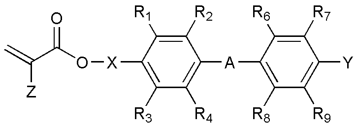
다 관능성 모노머 성분은 예를 들어, 하기 화학식 2로 표시되는 화합물을 포함할 수 있다. The multifunctional monomer component may include, for example, a compound represented by the following general formula (2).
[화학식 2] (2)
상기 화학식 2에서, A 및 A'는 각각 독립적으로 단일 결합, 알킬렌기, 알케닐렌기, 알콕실렌기, -COO-, -OCO- 또는 -O-이고, B는 페닐렌기 또는 싸이클로헥실렌기이며, X1 및 X2는 각각 독립적으로 단일결합, 알킬렌기 또는 알콕실렌기이고, R1 내지 R8은 각각 독립적으로 수소, 할로겐, 시아노기, 알킬기 또는 알콕시기이며, Z1 및 Z2는 각각 독립적으로 수소 또는 메틸기이다. In Formula 2, A and A 'each independently represents a single bond, an alkylene group, an alkenylene group, an alkoxysilyl group, -COO-, -OCO- or -O-, B represents a phenylene group or a cyclohexylene group , X 1 And X < 2 > are each independently Is a single bond, an alkylene group or an alkoxyl group xylene, R 1 to R 8 are independently hydrogen, halogen, a cyano group, an alkyl group or alkoxy group, respectively, Z 1 and Z 2 each independently is hydrogen or a methyl group.
화학식 2에서 A 및 A'에 대한 예들은 화학식 1의 A 항목에서 기술한 내용이 동일하게 적용될 수 있다. 다만, 하나의 구체적인 예로, 화학식 2에서 A 및 A'는 -COO-일 수 있고, 이 경우 A는 탄소가 B에 결합되고, 산소가 우측 벤젠 고리에 결합될 수 있으며, A'는 산소가 좌측 벤젠 고리에 결합될 수 있고, 탄소가 우측 벤젠 고리에 결합될 수 있다.Examples of A and A 'in the general formula (2) can be similarly applied to those described in the item (A) of the general formula (1). In one specific example, A and A 'in formula (2) may be -COO-, in which case A may be bonded to B and oxygen may be bonded to the right benzene ring, and A' Benzene ring, and carbon may be attached to the right benzene ring.
화학식 2에서 B가 페닐렌기인 경우, 예를 들어, 1,4-페닐렌기일 수 있다. 한편, 화학식 2에서 B가 사이클로헥실렌기인 경우, 예를 들어, 트랜스-1,4-사이클로헥실렌기일 수 있다. 하나의 구체적인 예로, 화학식 2에서 B는 1,4-페닐렌기일 수 있다. When B in the general formula (2) is a phenylene group, it may be, for example, a 1,4-phenylene group. On the other hand, when B in the formula (2) is a cyclohexylene group, it may be, for example, a trans-1,4-cyclohexylene group. In one specific example, in formula (2), B may be a 1,4-phenylene group.
화학식 2에서 X1 및 X2에 대한 예들은 화학식 1의 X 항목에서 기술한 내용이 동일하게 적용될 수 잇다. 다만, 하나의 구체적인 예로, X1 및 X2는 각각 탄소수 2개, 3개, 4개, 5개, 6개, 7개, 8개, 9개 또는 10개의 알콕시기 일 수 있고, X1은 산소가 B에 결합된 상태로 존재할 수 있고, X2는 산소가 벤젠 고리에 결합된 상태로 존재할 수 있다. Examples of X 1 and X 2 in the general formula (2) are the same as those described in the item X of the general formula (1). However, one specific example, X 1 and X 2 may each be a carbon number of two, three, four, five, six, seven, eight, nine or ten alkoxy groups, X 1 is Oxygen may be present bonded to B, and X < 2 > may be present in which oxygen is bonded to the benzene ring.
화학식 2에서 R1 내지 R8에 대한 예들은 화학식 1의 R1 내지 R8 항목에서 기술한 내용이 동일하게 적용될 수 있다. 하나의 예로, R1 내지 R8 중 어느 하나는 메틸기일 수 있고, 구체적으로 예를 들면, R1이 메틸기이고, R2 내지 R8은 수소일 수 있다. 또한, 하나의 구체적인 예로, 화학식 2의 Z1 및 Z2는 각각 수소일 수 있다. Examples of R 1 to R 8 in the general formula (2) include R 1 to R 8 The items described in the item can be applied equally. As one example, any one of R 1 to R 8 may be a methyl group, and specifically, for example, R 1 may be a methyl group and R 2 to R 8 may be hydrogen. Further, in one specific example, Z 1 and Z 2 in formula ( 2) may each be hydrogen.
수직 배향막Vertical alignment film
본 출원의 수직 배향막은 액정에 대하여 수직 배향력을 나타낼 수 있다. 본 명세서에서 용어 「수직」은 목적하는 효과를 손상시키지 않은 범위에서의 실질적인 수직을 의미한다. 따라서, 상기 용어는, 예를 들면, ±15도 이내, ±10도 이내, ±5도 이내 또는 ±3도 이내의 오차를 포함할 수 있다.The vertical alignment film of the present application can exhibit a vertical alignment force with respect to the liquid crystal. As used herein, the term " vertical " means a substantial vertical extent to the extent that the desired effect is not impaired. Therefore, the above term may include, for example, errors within ± 15 degrees, within ± 10 degrees, within ± 5 degrees, or within ± 3 degrees.
수직 배향막은 광 경화성 액정 화합물을 광 경화된 상태로 포함할 수 있다. 하나의 예시에서, 광 경화성 액정 화합물은 수직 배향막 평면에 대하여 약 75 내지 90 범위 내의 경사각을 이루도록 광 경화된 상태로 존재할 수 있다. 본 명세서에서 용어 「경사각」은 광 경화성 액정 화합물의 광축과 수직 배향막 평면이 이루는 최소각을 의미할 수 있다. 또한, 본 명세서에서 용어 「광축」은 액정 화합물이 막대 (rod) 모양인 경우 액정 화합물의 장축 방향의 축을 의미할 있고, 액정 화합물이 원판 (discotic) 모양인 경우 원판 평면의 법선 방향의 축을 의미할 수 있다The vertical alignment layer may contain a photo-curable liquid crystal compound in a photo-cured state. In one example, the photo-curable liquid crystal compound may be in a photo-cured state to provide an angle of inclination within the range of about 75 to 90 relative to the vertical alignment film plane. In this specification, the term " tilt angle " may mean a minimum angle formed by the optical axis of the photo-curable liquid crystal compound and the plane of the vertical alignment film. The term " optical axis " in the present specification means an axis in the long axis direction of the liquid crystal compound when the liquid crystal compound is a rod shape, and an axis in the normal direction of the disk plane when the liquid crystal compound is a discotic shape. Can
수직 배향막의 두께는, 예를 들어, 약 10 nm 내지 250 nm 범위 내일 수 있다. 후술하는 바와 같이, 수직 배향막이 기재를 추가로 포함하는 경우, 상기 두께 범위는, 기재를 제외한 광 경화된 상태로 존재하는 광 경화성 액정 화합물의 층의 두께를 의미한다. 수직 배향막의 두께는 보다 구체적으로, 10 nm 이상, 12.5 nm 이상, 15 nm 이상, 17.5 nm 이상, 20 nm 이상, 22.5 nm 이상, 25 nm 이상, 27.5 nm 이상, 30 nm 이상, 32.5 nm 이상, 35 nm 이상, 37.5 nm 이상, 40 nm 이상, 42.5 nm 이상, 45 nm 이상 또는 47.5 nm 이상일 수 있고, 250 nm 이하, 240 nm 이하, 230 nm 이하, 220 nm 이하, 210 nm 이하, 200 nm 이하, 190 nm 이하, 180 nm 이하, 170 nm 이하, 160 nm 이하, 150 nm 이하, 140 nm 이하, 130 nm 이하, 120 nm 이하 또는 110 nm 이하일 수 있다. 수직 배향막의 두께가 상기 범위 내인 경우 액정에 대한 수직 배향을 효과적으로 유도할 수 있다. The thickness of the vertical alignment film can be, for example, in the range of about 10 nm to 250 nm. As will be described later, when the vertical alignment film further comprises a substrate, the thickness range means the thickness of the layer of the photocurable liquid crystal compound existing in a photocured state excluding the substrate. More specifically, the thickness of the vertical alignment layer is preferably 10 nm or more , 12.5 nm or more, 15 nm or more, 17.5 nm or more, 20 nm or more, 22.5 nm or more, 25 nm or more, 27.5 nm or more, 30 nm or more, 250 nm or less, 240 nm or less, 230 nm or less, 220 nm or less, 210 nm or less, 200 nm or less, 190 nm or less, or about 190 nm or more, or less, 180 nm or less, 170 nm or less, 160 nm or less, 150 nm or less, 140 nm or less, 130 nm or less, 120 nm or less or 110 nm or less. When the thickness of the vertical alignment layer is within the above range, the vertical alignment with respect to the liquid crystal can be effectively induced.
수직 배향막은 기재를 추가로 포함할 수 있다. 이 경우, 광 경화성 액정 화합물은 상기 기재 상에 광 경화된 상태로 존재할 수 있다. 도 1 은 기재(102) 및 상기 기재 상에 인접하여 존재하는 광 경화성 액정 화합물의 광경화층(101)을 포함하는 수직 배향막(10)을 예시적으로 나타낸다. The vertical alignment film may further include a substrate. In this case, the photo-curable liquid crystal compound may be present in the photo-cured state on the substrate. Fig. 1 exemplarily shows a
기재로는 특별한 제한 없이 공지의 소재를 사용할 수 있다. 예를 들면, 유리 기재, 결정성 또는 비결정성 실리콘 필름, 석영 또는 ITO(Indium Tin Oxide) 필름 등의 무기계 필름이나 플라스틱 필름 등을 사용할 수 있다. 기재로는, 또한, 광학적으로 등방성인 기재 또는 위상차층과 같이 광학적으로 이방성인 기재를 사용할 수 있다. 기존 폴리이미드계 열 경화성 수직 배향막의 경우 소성 온도가 높고 소성 시간이 길어서 PET 또는 PC 기반의 플라스틱 필름 기재에 적용하는 것에 제한이 있는 반면, 본 출원의 광 경화성 수직 배향막은 후술하는 바와 같이 상대적으로 낮은 온도 및 짧은 시간으로 수행되는 용매의 건조 및 광 경화 공정을 통하여 형성이 가능하므로 유리 기재 뿐만 아니라 플라스틱 필름 기재에도 적용이 용이하다.As the substrate, known materials can be used without any particular limitation. For example, inorganic films such as glass substrates, crystalline or amorphous silicon films, quartz or indium tin oxide (ITO) films, and plastic films can be used. As the base material, an optically isotropic base material or an optically anisotropic base material such as a retardation layer can be used. Conventional polyimide-based thermosetting vertical alignment films have a high firing temperature and a long firing time and thus are limited to application to PET or PC-based plastic film substrates. On the other hand, the photo-curable vertical alignment film of the present application has a relatively low And can be formed through a drying and photocuring process of a solvent which is carried out at a low temperature and a short time, so that it is easy to apply to a plastic film substrate as well as a glass substrate.
플라스틱 필름 기재의 구체적인 예로, TAC(triacetyl cellulose); 노르보르넨 유도체 등의 COP(cyclo olefin copolymer); PMMA(poly(methyl methacrylate); PC(polycarbonate); PE(polyethylene); PP(polypropylene); PVA(polyvinyl alcohol); DAC(diacetyl cellulose); Pac(Polyacrylate); PES(poly ether sulfone); PEEK(polyetheretherketon); PPS(polyphenylsulfone), PEI(polyetherimide); PEN(polyethylenemaphthatlate); PET(polyethyleneterephtalate); PI(polyimide); PSF(polysulfone); PAR(polyarylate) 또는 비정질 불소 수지 등을 포함하는 기재 필름이 예시될 수 있지만 이에 제한되는 것은 아니다. 기재에는, 필요에 따라서 금, 은, 이산화 규소 또는 일산화 규소 등의 규소 화합물의 코팅층이나, 반사 방지층 등의 코팅층이 존재할 수도 있다.Specific examples of the plastic film substrate include TAC (triacetyl cellulose); A cycloolefin copolymer (COP) such as a norbornene derivative; Poly (methyl methacrylate), PC (polycarbonate), polyethylene (PE), polypropylene (PVP), polyvinyl alcohol (PVA), diacetyl cellulose (DAC), polyacrylate (PAC), polyether sulfone (PES) A substrate film including polyphenylsulfone (PPS), polyetherimide (PEI), polyethylenemaphthatate (PET), polyimide (PET), polysulfone (PS), polyarylate A coating layer of a silicon compound such as gold, silver, silicon dioxide or silicon monoxide, or a coating layer such as an antireflection layer may be present on the substrate.
수직 배향막의 제조 방법Method of manufacturing vertical alignment film
본 출원은 또한, 수직 배향막의 제조 방법에 관한 것이다. 상기 제조 방법은 예를 들어, 전술한 수직 배향막을 제조할 수 있다. 본 출원의 예시적인 수직 배향막의 제조 방법은 기재상에 마련된 수직 배향막 조성물의 층을 광 경화하는 것을 포함할 수 있다. 하나의 예시에서, 상기 수직 배향막 조성물로는 광 경화성 액정 화합물의 농도가 약 1 중량% 이상 내지 약 5 중량% 미만인 수직 배향막 조성물을 사용할 수 있다. 상기 제조 방법에서, 기재 및 광경화성 액정 화합물에 대한 구체적인 사항은 수직 배향막의 항목에서 기술한 내용이 동일하게 적용될 수 있다. The present application also relates to a method of manufacturing a vertical alignment film. The above manufacturing method can, for example, produce the aforementioned vertical alignment film. Exemplary methods of making vertical alignment films of the present application can include photocuring a layer of a vertical alignment film composition provided on a substrate. In one example, the vertical alignment film composition may be a vertical alignment film composition having a concentration of the photocurable liquid crystal compound of about 1 wt% or more to less than about 5 wt%. In the above manufacturing method, details of the substrate and the photo-curable liquid crystal compound can be applied equally to those described in the item of the vertical alignment film.
수직 배향막 조성물은 광 경화성 액정 화합물을 포함하되, 광 경화성 액정 화합물의 농도가 약 1 중량% 이상 내지 약 5 중량% 미만이 되도록 포함할 수 있다. 본 명세서에서 특별한 언급이 없는 한 농도는 중량 백분율(weight percent)를 의미한다. 즉, 수직 배향막 조성물에서 광 경화성 액정 화합물의 농도가 약 1 중량% 이상 내지 5 중량% 미만이라는 것은, 전체 수직 배향막 조성물 100 중량부 대비 광 경화성 액정 화합물이 1 중량부 이상 내지 5 중량부 미만의 비율로 포함된다는 것을 의미한다. 또한, 상기에서 광 경화성 액정 화합물의 비율은 고형분 상태의 중량을 기준으로 한다. 보다 구체적으로, 수직 배향막 조성물에서 광 경화성 액정 화합물의 농도는 약 1 중량% 이상, 1.2 중량% 이상, 1.4 중량% 이상, 1.6 중량% 이상, 1.8 중량% 이상 또는 2.0 중량% 이상일 수 있고, 5 중량% 미만, 4.8 중량% 이하, 4.6 중량% 이하, 4.4 중량% 이하, 4.2 중량% 이하, 4.0 중량% 이하, 3.8 중량% 이하, 3.6 중량% 이하, 3.4 중량% 이하, 3.2 중량% 이하, 3.0 중량% 이하, 2.8 중량% 이하, 2.6 중량% 이하, 2.4 중량% 이하 또는 2.2 중량% 이하일 수 있다. 광 경화성 액정 화합물의 농도가 상기 범위 내인 경우 액정에 대한 수직 배향을 효과적으로 유도하는 수직 배향막을 제조할 수 있다. The vertical alignment film composition may include a photocurable liquid crystal compound such that the concentration of the photocurable liquid crystal compound is from about 1% by weight to less than about 5% by weight. Unless otherwise specified herein, the concentration means the weight percent. That is, the reason why the concentration of the photo-curable liquid crystal compound in the vertical alignment film composition is less than about 1 wt% to less than 5 wt% is that the photo-curable liquid crystal compound is contained in an amount of 1 to 5 parts by weight . ≪ / RTI > The proportion of the photo-curable liquid crystal compound in the above is based on the weight in the solid state. More specifically, the concentration of the photo-curable liquid crystal compound in the vertical alignment film composition may be at least about 1 wt%, at least about 1.2 wt%, at least about 1.4 wt%, at least about 1.6 wt%, at least about 1.8 wt%, or at least about 2.0 wt% Not more than 4.8 wt%, not more than 4.6 wt%, not more than 4.4 wt%, not more than 4.2 wt%, not more than 4.0 wt%, not more than 3.8 wt%, not more than 3.6 wt%, not more than 3.4 wt% Or less, 2.8 wt% or less, 2.6 wt% or less, 2.4 wt% or less, or 2.2 wt% or less. When the concentration of the photo-curable liquid crystal compound is within the above range, a vertical alignment film that effectively induces vertical alignment to the liquid crystal can be produced.
광 경화성 액정 화합물을 농도를 상기 범위로 조절하는 방법은 본 출원의 목적을 손상시키지 않는 범위 내에서 적절히 채용하여 사용할 수 있다. 하나의 예로, 광 경화성 액정 화합물을 용매로 희석시켜 사용할 수 있다. 이하, 수직 배향막 조성물에서 광 경화성 액정 화합물 및 기타 첨가제를 제외한 용매를 잔부 용매로 호칭할 수 있다. 잔부 용매로는 예를 들어, 통상적인 유기 용매를 사용할 수 있다. 유기 용매로는 예를 들어, 에테르 용매, 방향족 용매, 할로겐 용매, 올레핀 용매 또는 케톤 용매 등의 1종 또는 2종 이상이 예시될 수 있으며, 구체적으로는, 시클로펜타논, 시클로 헥사논, 클로로벤젠, N-메틸피롤리돈, 톨루엔, 자일렌, 메시틸렌, 시멘, 디메틸설폭사이드, 디메틸포름아미드, 클로로포름, 감마부티로락톤 또는 테트라히드로푸란 등이 예시될 수 있다. 본 출원의 일 실시예로, 잔부 용매로 톨루엔, 시클로 헥사논 등을 선택하여 사용할 수 있으나, 이에 제한되는 것은 아니다. The method of controlling the concentration of the photo-curable liquid crystal compound in the above-described range can be suitably employed within the range not impairing the object of the present application. As one example, the photo-curable liquid crystal compound can be used by diluting with a solvent. Hereinafter, the solvent excluding the photo-curable liquid crystal compound and other additives in the vertical alignment film composition may be referred to as the residual solvent. As the remaining solvent, for example, a conventional organic solvent may be used. Examples of the organic solvent include an ether solvent, an aromatic solvent, a halogen solvent, an olefin solvent, and a ketone solvent. Specific examples thereof include cyclopentanone, cyclohexanone, chlorobenzene , N-methylpyrrolidone, toluene, xylene, mesitylene, cymene, dimethylsulfoxide, dimethylformamide, chloroform, gamma butyrolactone or tetrahydrofuran. In one embodiment of the present application, toluene, cyclohexanone, and the like can be selected and used as the residual solvent, but the present invention is not limited thereto.
수직 배향막 조성물은 광 개시제를 추가로 포함할 수 있다. 광 개시제로는 예를 들어 라디칼 중합을 개시할 수 있는 광 개시제 사용할 수 있다. 이러한 개시제로는 예를 들어, 옥심에스테르계, 벤조페논계, α-아미노케논계 또는 아크릴포스핀옥사이드계 등의 개시제를 사용할 수 있으나, 이에 제한되는 것은 아니다. 수직 배향막 조성물 내의 광 개시제의 비율은 본 출원의 목적을 손상시키지 않는 범위 내에서 적절히 선택될 수 있다. 예를 들어, 광 개시제는 광 경화성 액정 화합물 100 중량부 대비 약 1 중량부 내지 약 5 중량부 비율로 포함될 수 있다. 보다 구체적으로, 광 개시제는 광 경화성 액정 화합물 100 중량부 대비, 1 중량부 이상, 1.5 중량부 이상, 2.0 중량부 이상 또는 2.5 중량부 이상 및 5 중량부 이하, 4.5 중량부 이하, 4.0 중량부 이하, 3.5 중량부 이하, 3.0 중량부 이하 또는 2.5 중량부 이하의 비율로 포함될 수 있다. The vertical alignment film composition may further comprise a photoinitiator. As the photoinitiator, for example, a photoinitiator capable of initiating radical polymerization can be used. Examples of the initiator include, but are not limited to, oxime ester-based, benzophenone-based,? -Aminoquinone-based, or acrylphosphine oxide-based initiators. The proportion of the photoinitiator in the vertical alignment film composition can be suitably selected within a range that does not impair the purpose of the present application. For example, the photoinitiator may be included in an amount of about 1 part by weight to about 5 parts by weight based on 100 parts by weight of the photocurable liquid crystal compound. More specifically, the photoinitiator is used in an amount of 1 part by weight or more, 1.5 parts by weight or more, 2.0 parts by weight or more, or 2.5 parts by weight or more and 5 parts by weight or less, 4.5 parts by weight or less and 4.0 parts by weight or less , 3.5 parts by weight or less, 3.0 parts by weight or less, or 2.5 parts by weight or less.
기재 상에 수직 배향막 조성물의 층을 마련하는 방식은 특별히 제한되지 않고, 예를 들어, 공지의 코팅 방식을 채용할 수 있다. 코팅 방식의 구체적인 예로는, 예를 들면, 롤 코팅, 인쇄법, 잉크젯 코팅, 슬릿 노즐법, 바 코팅, 콤마 코팅, 스핀 코팅 또는 그라비어 코팅 등이 예시될 수 있으나, 이에 제한되는 것은 아니다. 수직 배향막 조성물의 층은 기재 상에 예를 들어, 약 2 um 내지 10 um 범위 내의 두께로 형성할 수 있으나, 이에 제한되는 것은 아니다. 본 출원의 일 실시예에 의하면, 기재 상에 마련되는 수직 배향막 조성물의 층의 두께를 용이하게 조절하는 측면에서 메이어 바 코팅 방식을 채용할 수 있으나, 이에 제한되는 것은 아니다.The manner of providing the layer of the vertical alignment film composition on the substrate is not particularly limited, and for example, a known coating method may be employed. Specific examples of the coating method include, but are not limited to, roll coating, printing, ink jet coating, slit nozzle method, bar coating, comma coating, spin coating or gravure coating. The layer of the vertical alignment film composition may be formed on the substrate, for example, to a thickness within the range of from about 2 [mu] m to about 10 [mu] m, but is not limited thereto. According to one embodiment of the present invention, Meyer bar coating may be employed in order to easily control the thickness of the layer of the vertical alignment film composition provided on the substrate, but the present invention is not limited thereto.
상기 제조 방법은 광 경화하기 전에 용매의 건조 단계를 추가로 포함할 수 있다. 따라서, 상기 방법에 의해 제조되는 수직 배향막은 용매를 포함하지 않으면서 광 경화성 액정 화합물을 광 경화된 상태로 포함할 수 있다. 하나의 구체적인 예로, 수직 배향막 조성물의 층의 용매를 건조하는 공정은 약 150℃ 이하, 140℃ 이하, 130℃ 이하, 120℃ 이하 110℃이하 또는 100 ℃ 이하의 온도에서 수행될 수 있고, 또한 약 10분 이내, 8분 이내, 6분 이내, 4분 이내 또는 2분 이내의 시간 동안 수행될 수 있다. 기존의 폴리이미드계 열경화 타입 수직 배향막의 경우 소성 온도가 높고 소성 시간이 길어서 PET 또는 PC 기반의 플라스틱 필름 기재에 적용하는 것에 제한이 있는 반면, 본 출원의 수직 배향막은 상기와 같이 상대적으로 낮은 온도 및 짧은 시간으로 수행되는 용매의 건조 및 광 경화 공정을 통하여 형성이 가능하므로 유리 기재뿐만 아니라 플라스틱 필름 기재에도 적용이 용이하며, 롤투롤 공정에도 적용될 수 있는 장점이 있다. The process may further comprise a drying step of the solvent prior to photo-curing. Therefore, the vertical alignment layer produced by the above method can include the photo-curable liquid crystal compound in a photo-cured state without containing a solvent. In one specific example, the step of drying the solvent of the layer of the vertical alignment film composition may be performed at a temperature of about 150 ° C or less, 140 ° C or less, 130 ° C or less, 120 ° C or less, 110 ° C or less, Less than 10 minutes, less than 8 minutes, less than 6 minutes, less than 4 minutes, or less than 2 minutes. The conventional polyimide-based thermosetting type vertical alignment film has a high firing temperature and a long firing time, which is a limitation in application to PET or PC-based plastic film substrates, whereas the vertical alignment film of the present application has a relatively low temperature And drying and photo-curing processes of a solvent to be performed in a short time. Therefore, it is easy to apply to a glass substrate as well as a plastic film substrate, and can be applied to a roll-to-roll process.
상기 제조 방법에서, 수직 배향막 조성물의 층을 광 경화하는 것은 광 경화를 유도할 수 있는 적절한 에너지, 예를 들면 광을 조사하여 수행할 수 있다. 하나의 구체적인 예로, 광 경화는 수직 배향막 조성물의 층에 자외선을 조사하는 것에 의하여 수행될 수 있다. 광 경화를 위한 자외선은 약 100 mJ/cm2 내지 약 2 J/cm2 범위 내의 세기로 조사될 수 있다. 보다 구체적으로, 광 경화를 위한 자외선은 약 100 mJ/cm2 이상, 200 mJ/cm2 이상, 300 mJ/cm2 이상, 400 mJ/cm2 이상, 500 mJ/cm2 이상, 600 mJ/cm2 이상, 약 700 mJ/cm2 이상, 약 800 mJ/cm2 이상, 약 900 mJ/cm2 이상 및 약 2 J/cm2 이하, 1900 mJ/cm2 이하, 1800 mJ/cm2 이하, 1700 mJ/cm2 이하, 1600 mJ/cm2 이하, 1500 mJ/cm2 이하, 1400 mJ/cm2 이하, 1300 mJ/cm2 이하, 1200 mJ/cm2 이하 또는 1100 mJ/cm2 이하의 범위 내로 조사될 수 있고, 본 출원의 일 실시예에 의하면, 약 1J의 세기로 조사될 수 있으나, 이에 제한되는 것은 아니다. 자외선 세기를 상기 범위로 조절하는 경우 액정에 대한 수직 배향을 효과적으로 유도하는 수직 배향막을 제조할 수 있다.In the above manufacturing method, the photo-curing of the layer of the vertical alignment film composition can be carried out by irradiating with appropriate energy capable of inducing photo-curing, for example, light. In one specific example, photo-curing may be performed by irradiating ultraviolet light to the layer of the vertical alignment film composition. Ultraviolet light for photo-curing may be irradiated at an intensity in the range of about 100 mJ / cm 2 to about 2 J / cm 2 . More specifically, the ultraviolet light for photo-curing is at least about 100 mJ / cm 2 , at least 200 mJ / cm 2, at least 300 mJ / cm 2, at least 400 mJ / cm 2, at least 500 mJ / cm 2 , 2, at least about 700 mJ / cm 2, greater than or equal to about 800 mJ / cm 2, greater than or equal to about 900 mJ / cm 2 or more and about 2 J / cm 2 or less, 1900 mJ / cm 2 or less, 1800 mJ / cm 2 or less, 1700 mJ / cm 2 or less, 1600 mJ / cm 2 or less, 1500 mJ / cm 2 or less, 1400 mJ / cm 2 or less, 1300 mJ / cm 2 or less, 1200 mJ / cm 2 or less, or 1100 mJ / cm 2 range up into And according to one embodiment of the present application, can be examined with an intensity of about 1 J, but it is not so limited. When the ultraviolet intensity is adjusted to the above range, a vertical alignment film which effectively induces the vertical alignment to the liquid crystal can be manufactured.
상기 제조 방법에 있어서, 수직 배향막 조성물의 층의 광 경화 후 두께는 예를 들어, 약 10 nm 내지 250 nm 범위 내가 되도록 조절될 수 있다. 수직 배향막 조성물의 층의 광 경화 후 두께는 보다 구체적으로, 10 nm 이상, 12.5 nm 이상, 15 nm 이상, 17.5 nm이상, 20 nm 이상, 22.5 nm 이상, 25 nm 이상, 27.5 nm 이상, 30 nm 이상, 32.5 nm 이상, 35 nm 이상, 37.5 nm 이상, 40 nm 이상, 42.5 nm 이상, 45 nm 이상 또는 47.5 nm 이상일 수 있고, 250 nm 이하, 240 nm 이하, 230 nm 이하, 220 nm 이하, 210 nm 이하, 200 nm 이하, 190 nm 이하, 180 nm 이하, 170 nm 이하, 160 nm 이하, 150 nm 이하, 140 nm 이하, 130 nm 이하, 120 nm 이하 또는 110 nm 이하일 수 있다. 광 경화 후 수직 배향막 조성물의 두께를 상기 범위로 조절하는 경우 액정에 대한 수직 배향을 효과적으로 유도할 수 있다. 수직 배향막 조성물의 층의 광 경화 후 두께를 상기 범위 내로 조절하는 방식은 특별히 제한되지 않고 공지의 코팅 두께 조절 방식을 채용할 수 있다. 본 출원의 일 실시예에 의하면, 메이어 바를 통하여 코팅 두께를 조절할 수 있으나, 이러한 방식에 제한되는 것은 아니다.In the above manufacturing method, the thickness of the layer of the vertical alignment film composition after photo-curing can be adjusted to be, for example, in the range of about 10 nm to 250 nm. More specifically, the thickness of the layer of the vertical alignment film composition after the photo-curing is at least 10 nm, at least 12.5 nm, at least 15 nm, at least 17.5 nm, at least 20 nm, at least 22.5 nm, at least 25 nm, at least 27.5 nm, at least 30 nm , 32.5 nm or more, 35 nm or more, 37.5 nm or more, 40 nm or more, 42.5 nm or more, 45 nm or more, or 47.5 nm or more and 250 nm or less, 240 nm or less, 230 nm or less, 220 nm or less and 210 nm or less 190 nm or less, 180 nm or less, 170 nm or less, 160 nm or less, 150 nm or less, 140 nm or less, 130 nm or less, 120 nm or less or 110 nm or less. When the thickness of the vertical alignment film composition is adjusted to the above range after photo-curing, the vertical alignment of the liquid crystal can be effectively induced. The method of adjusting the thickness of the layer of the vertical alignment film composition after the photo-curing is within the above-mentioned range is not particularly limited and a known coating thickness control method may be adopted. According to one embodiment of the present application, the thickness of the coating can be controlled through the Meyer bar, but is not limited thereto.
수직 배향막의 용도Uses of Vertical Orientation Film
본 출원은 또한 상기 수직 배향막의 용도에 관한 것이다. 상기 수직 배향막은 액정의 수직 배향이 요구되는 모든 광학 소자에 적용될 수 있다. 예시적인 광학 소자는 도 2에 도시한 바와 같이, 대향 배치된 2 장의 수직 배향막(10A, 10B) 및 상기 2 장의 수직 배향막 사이에 존재하고 액정 화합물을 포함하는 액정층(201)을 가질 수 있다. 이하, 수직 배향막의 광 경화성 액정 화합물과 구분을 위하여 광학 소자의 액정층 내에 포함되는 액정 화합물을 제 2 액정 화합물로 호칭한다. The present application also relates to the use of said vertical alignment film. The vertical alignment film can be applied to all optical devices requiring vertical alignment of the liquid crystal. The exemplary optical element may have two
액정층 내의 제 2 액정 화합물은 초기 상태에서 수직 배향된 상태로 존재할 수 있다. 즉, 제 2 액정 화합물은 수직 배향막의 수직 배향력에 의하여 수직 배향된 상태로 액정층 내에 존재할 수 있다. 명세서에서 용어 「초기 상태」는 외부 작용이 없는 상태를 의미할 수 있고, 상기 용어 「외부 작용」은 액정 화합물의 정렬을 변경시킬 수 있도록 수행되는 모든 종류의 작용을 의미하고, 대표적인 예로는 전압의 인가가 있다. The second liquid crystal compound in the liquid crystal layer may exist in a vertically aligned state in an initial state. That is, the second liquid crystal compound may exist in the liquid crystal layer in the state of being vertically oriented by the vertical orientation force of the vertical alignment film. The term " initial state " in the specification may mean a state without external action, and the term " external action " means any kind of action performed to change the alignment of the liquid crystal compound, There is authorization.
제 2 액정 화합물로는 광학 소자의 용도에 따라 경화성 관능기를 가지는 경화성 액정 화합물 또는 경화성 관능기를 가지지 않는 비 경화성 액정 화합물을 사용할 수 있다. 하나의 예로, 제 2 액정 화합물로 경화성 액정 화합물을 사용하는 경우 그 배향을 고정시켜 사용하는 것에 유리 하다. 또는 다른 하나의 예로, 외부 작용 인가 여부에 따라 액정 화합물의 배향을 스위칭함으로써 광학 소자의 광 변조 특성을 조절한다는 측면에서 비 경화성 액정 화합물을 사용할 수도 있다. 상기 제 2 액정 화합물로는 예를 들면, 스멕틱(smectic) 액정 화합물, 네마틱(nematic) 액정 화합물 또는 콜레스테릭(cholesteric) 액정 화합물 등을 사용할 수 있다. As the second liquid crystal compound, a curable liquid crystal compound having a curable functional group or a non-curable liquid crystal compound having no curable functional group may be used depending on the use of the optical element. As an example, when a curable liquid crystal compound is used as the second liquid crystal compound, it is advantageous to use the liquid crystal compound with its orientation fixed. Alternatively, a non-curable liquid crystal compound may be used in view of controlling the light modulation characteristics of the optical element by switching the orientation of the liquid crystal compound depending on whether external action is applied or not. The second liquid crystal compound may be, for example, a smectic liquid crystal compound, a nematic liquid crystal compound or a cholesteric liquid crystal compound.
액정층은 또한 폴리머 네트워크를 추가로 포함할 수 있다. 폴리머 네트워크는, 예를 들면, 액정셀의 헤이즈 또는 투과도 특성을 조절하기 위하여 추가로 포함될 수 있다. 액정층이 폴리머 네트워크를 포함하는 경우 제 2 액정 화합물로는 비 경화성 액정 화합물을 사용할 수 있다. 이 경우, 제 2 액정 화합물은 폴리머 네트워크와는 결합되어 있지 않으며 외부에서 전압이 인가될 경우에 그에 따라서 배향이 변경될 수 있는 형태일 수 있다. 하나의 예시에서, 제 2 액정 화합물은 폴리머 네트워크와 상분리된 상태로, 폴리머 네트워크 내에 분산된 상태로 존재할 수 있다. 액정층 내의 폴리머 네트워크는 폴리머 네트워크가 연속상의 액정 화합물 중에 분포되어 있는 구조, 소위 PNLC(Polymer Network Liquid Crystal) 구조로 액정층 내에 포함될 수 있고, 또는, 폴리머 네트워크 내에 액정 화합물을 포함하는 액정 영역이 분산되어 있는 상태로 존재하는 구조, 소위 PDLC(Polymer Dispersed Liquid Crystal) 구조로 액정층 내에 포함될 수 있다. The liquid crystal layer may further comprise a polymer network. The polymer network may further be included, for example, to control the haze or transmittance characteristics of the liquid crystal cell. When the liquid crystal layer includes a polymer network, a non-curable liquid crystal compound may be used as the second liquid crystal compound. In this case, the second liquid crystal compound is not bonded to the polymer network and may be in a form in which the orientation can be changed accordingly when a voltage is applied from the outside. In one example, the second liquid crystal compound may be dispersed within the polymer network, phase separated from the polymer network. The polymer network in the liquid crystal layer may be contained in the liquid crystal layer in a structure in which a polymer network is distributed in a continuous liquid crystal compound, that is, a so-called PNLC (Polymer Network Liquid Crystal) structure, or a liquid crystal region containing a liquid crystal compound is dispersed (Polymer Dispersed Liquid Crystal) structure, which is present in a state in which a liquid crystal layer is present.
폴리머 네트워크는, 예를 들면 중합성 화합물을 포함하는 전구 물질의 네트워크일 수 있다. 따라서, 폴리머 네트워크는 중합된 상태로 중합성 화합물을 포함할 수 있다. 중합성 화합물로는, 액정성을 나타내지 않는 비액정성 화합물이 사용될 수 있다. 중합성 화합물로는, 소위 PDLC 또는 PNLC 소자의 폴리머 네트워크를 형성할 수 있는 것으로 알려진 하나 이상의 중합성 관능기를 가지는 화합물 또는 필요한 경우 중합성 관능기가 없는 비중합성 화합물을 사용할 수 있다. 전구 물질에 포함될 수 있는 중합성 화합물로 아크릴레이트 화합물 등이 예시할 수 있으나 이에 제한되는 것은 아니다. The polymer network may be, for example, a network of precursors comprising polymeric compounds. Thus, the polymer network may comprise polymeric compounds in a polymerized state. As the polymerizable compound, a non-liquid crystalline compound which does not exhibit liquid crystallinity can be used. As the polymerizable compound, a compound having at least one polymerizable functional group known to be capable of forming a polymer network of a so-called PDLC or PNLC device or a non-polymerizable compound having no polymerizable functional group, if necessary, can be used. Examples of the polymerizable compound that can be contained in the precursor include acrylate compounds and the like, but are not limited thereto.
폴리머 네트워크의 액정층 내의 비율은, 목적 물성, 예를 들면, 액정셀의 헤이즈 또는 투과도 특성 등을 고려하여 적절히 선택될 수 있다. 폴리머 네트워크는, 예를 들어, 40 중량% 이하, 38 중량% 이하, 36 중량% 이하, 34 중량% 이하, 32 중량%이하 또는 30 중량% 이하의 비율로 액정층 내에 포함될 수 있다. 폴리머 네트워크의 액정층 내의 비율의 하한은 특별히 제한되지 않으나, 예를 들어, 0.1 중량% 이상, 1 중량%, 2 중량% 이상, 3 중량% 이상, 4 중량% 이상, 5 중량% 이상, 6 중량% 이상, 7 중량% 이상, 8 중량% 이상, 9 중량% 이상 또는 10 중량% 이상일 수 있다. The ratio in the liquid crystal layer of the polymer network can be appropriately selected in consideration of the target properties, for example, the haze or the transmittance characteristics of the liquid crystal cell. The polymer network may be included in the liquid crystal layer in a ratio of, for example, 40 wt% or less, 38 wt% or less, 36 wt% or less, 34 wt% or less, 32 wt% or less, or 30 wt% or less. The lower limit of the ratio in the liquid crystal layer of the polymer network is not particularly limited but may be, for example, 0.1 wt% or more, 1 wt%, 2 wt% or more, 3 wt% or more, 4 wt% or more, 5 wt% %, 7 wt% or more, 8 wt% or more, 9 wt% or more, or 10 wt% or more.
광학 소자는 기판을 추가로 포함할 수 있다. 하나의 예로, 광학 소자는 도 3에 도시한 바와 같이, 대향 배치된 2개의 기판(202A, 202B)을 포함하고, 액정층(201)은 상기 대향 배치된 2개의 기판의 사이에 존재할 수 있다. 액정셀이 대향 하는 2개의 기판을 포함하는 경우, 수직 배향막(10A, 10B)은 대향 배치된 2개의 기판의 내측, 즉 액정층 측면에 존재할 수 있다. 기판으로는, 특별한 제한 없이 공지의 소재를 사용할 수 있다. 예를 들어, 전술한 수직 배향막의 기재 소재를 적용할 수 있다. The optical element may further include a substrate. As one example, the optical element includes two
광학 소자는 전극층을 추가로 포함할 수 있다. 하나의 예로, 전극층은 액정층과 인접하게 배치될 수 있다. 예를 들어, 전극층(203A, 203B)은 도 4 에 나타낸 바와 같이, 대향하는 2개의 기판(202A, 202B)의 액정층(201) 측면에 존재할 수 있다. 이 경우, 수직 배향막(10A, 10B)은 대향 배치된 2개의 전극층의 내측, 즉 액정층 측면에 존재할 수 있다. 이러한 전극층은 액정층 내의 액정 화합물의 정렬 상태를 전환할 수 있도록 액정층에 수직 또는 수평 전계를 인가할 수 있다. 전극층은, 예를 들면, 전도성 고분자, 전도성 금속, 전도성 나노와이어 또는 ITO(Indium Tin Oxide) 등의 금속 산화물 등을 증착하여 형성할 수 있다. 전극층은, 투명성을 가지도록 형성될 수 있다. 이 분야에서는, 투명 전극층을 형성할 수 있는 다양한 소재 및 형성 방법이 공지되어 있고, 이러한 방법은 모두 적용될 수 있다. 필요한 경우에, 기판의 표면에 형성되는 전극층은, 적절하게 패턴화되어 있을 수도 있다. The optical element may further include an electrode layer. In one example, the electrode layer may be disposed adjacent to the liquid crystal layer. For example, as shown in Fig. 4, the electrode layers 203A and 203B may exist on the side surfaces of the
광학 소자는 전술한 수직 배향막의 제조 방법으로 형성된 수직 배향막 상에 전술한 제 2 액정 화합물을 포함하는 액정층 조성물 또는 상기 제 2 액정 화합물에 전술한 이색성 염료 및/또는 폴리머 네트워크 전구 물질을 추가로 포함하는 액정층 조성물을 형성하는 것에 의하여 제조할 수 있다. 또한, 액정층 조성물이 폴리머 네트워크 전구 물질을 포함하는 경우 이들의 중합을 위하여 적절한 에너지의 인가, 예를 들어 자외선을 조사하는 공정이 추가로 수행될 수 있다. 또한, 전술한 바와 같이 제 2 액정 화합물이 경화성 관능기를 가지는 경우에도 경화를 위하여, 적절한 에너지의 인가, 예를 들어, 광 또는 열 에너지를 조사하는 공정이 추가로 수행될 수 있다. The optical element may further include a liquid crystal layer composition comprising the above-described second liquid crystal compound on the vertical alignment film formed by the above-mentioned method of manufacturing the vertical alignment film, or the above-mentioned dichroic dye and / or polymer network precursor to the second liquid crystal compound To form a liquid crystal layer composition containing the liquid crystal composition. Further, in the case where the liquid crystal layer composition includes a polymer network precursor, application of appropriate energy, for example, ultraviolet light irradiation, may be further performed for polymerization of the precursor. Further, even in the case where the second liquid crystal compound has a curable functional group as described above, a process of irradiating with appropriate energy, for example, light or heat energy, may be further performed for curing.
액정층의 두께는 본 출원의 목적을 손상시키지 않는 범위 내, 에서 적절히 조절될 수 있다. 하나의 구체저인 예로, 액정층의 두께는 약 2um 내지 25um 범위 내일 수 있으나, 이에 제한되는 것은 아니다. 또한, 액정층은 초기 상태에서 하기 수식 A로 규정되는 면상 위상차 값이 예를 들어 100 nm 이하일 수 있고, 하기 수식 B로 규정되는 두께 방향 위상차 값이 예를 들어 200 nm 이상일 수 있으나, 상기 범위는 필요에 따라 적절히 조절될 수 있다. The thickness of the liquid crystal layer can be appropriately adjusted within a range that does not impair the purpose of the present application. In one embodiment, the thickness of the liquid crystal layer may be within the range of about 2 um to about 25 um, but is not limited thereto. In the initial state, the liquid crystal layer may have an in-plane retardation value defined by the following formula A, for example, 100 nm or less, and a thickness direction retardation value defined by the following formula B may be 200 nm or more, And can be appropriately adjusted as needed.
[수식 A][Formula A]
Rin = d (nx - ny)Rin = d (nx - ny)
[수식 B][Formula B]
Rth = d (nz - ny)Rth = d (nz - ny)
수식 A 또는 B에서, nx, ny 및 nz는 각각 액정층의 x, y 및 z 방향의 굴절률을 의미한다. 예를 들어, nx는 액정층의 평면에서 지상축 방향의 굴절률이며, ny는 액정층의 상기 지상축에 수직하는 방향의 굴절률이고, nz는 액정층의 두께 방향, 즉 상기 지상축과 그에 수직하는 방향 모두와 수직하는 방향의 굴절률을 의미할 수 있다. 본 명세성서 용어 「굴절률」은 특별히 달리 규정하지 않는 한, 550nm파장의 광에 대한 굴절률을 의미한다. In the formula A or B, n x , n y, and n z mean refractive indices in the x, y, and z directions, respectively, of the liquid crystal layer. For example, nx is the refractive index in the slow axis direction in the plane of the liquid crystal layer, ny is the refractive index in the direction perpendicular to the slow axis of the liquid crystal layer, and nz is the refractive index in the thickness direction of the liquid crystal layer, And the refractive index in a direction perpendicular to both directions. The term "refractive index" as used in this specification means the refractive index for light with a wavelength of 550 nm unless otherwise specified.
액정층은 이방성 염료를 추가로 포함할 수 있다. 본 명세서에서 용어 「염료」는, 가시광 영역, 예를 들면, 400 nm 내지 700 nm 파장 범위 내에서 적어도 일부 또는 전체 범위 내의 광을 집중적으로 흡수 및/또는 변형시킬 수 있는 물질을 의미할 수 있고, 용어 「이방성 염료」는 상기 가시광 영역의 적어도 일부 또는 전체 범위에서 광의 이방성 흡수가 가능한 물질을 의미할 수 있다. 상기와 같은 염료의 사용을 통해서 액정셀이 표시 장치에 적용되었을 경우에 장치의 색감을 조절할 수 있다. The liquid crystal layer may further include an anisotropic dye. As used herein, the term " dye " may refer to a material that is capable of intensively absorbing and / or deforming light within a visible light region, for example, within a wavelength range of 400 nm to 700 nm, The term " anisotropic dye " may mean a material capable of anisotropic absorption of light in at least a part or the entire range of the visible light region. When the liquid crystal cell is applied to a display device through the use of such a dye, the color of the device can be controlled.
이방성 염료의 종류는 특별히 제한되지 않으며, 예를 들면, 상기와 같은 특성을 가지면서 액정 화합물의 배향에 따라 배향될 수 있는 특성을 가지는 것으로 공지된 모든 종류의 염료가 사용될 수 있다. 이방성 염료로는, 예를 들면 흑색 염료(black dye) 또는 컬러 염료(color dye)를 사용할 수 있다. 상기 이방성 염료는, 이색비(dichroic ratio), 즉 이방성 염료의 장축 방향에 평행한 편광의 흡수를 상기 장축 방향에 수직하는 방향에 평행한 편광의 흡수로 나눈 값이 5 이상, 6 이상 또는 7 이상인 염료를 사용할 수 있다. 상기 염료는 가시광 영역의 파장 범위 내, 예를 들면, 약 380 nm 내지 700 nm 또는 약 400 nm 내지 700 nm의 파장 범위 내에서 적어도 일부의 파장 또는 어느 한 파장에서 상기 이색비를 만족할 수 있다. 상기 이색비는 높을수록 차단율 개선 또는 컬러 구현에 효과적이므로 상한은 특별히 제한되지 않고 의도하는 컬러 구현의 정도를 고려하여 적절한 이색비를 가지는 이방성 염료를 선택하여 사용할 수 있다. 또한, 액정층 내에서 이방성 염료의 비율은 본 출원의 목적을 손상시키지 않는 범위 내에서 적절히 선택될 수 있다. 예를 들어, 이방성 염료는 제 액정 화합물 100 중량부 대비 0.01 중량부 내지 5 중량부 정도의 비율로 포함될 수 있으나, 상기 비율은 필요에 따라 적정 범위로 변경될 수 있다. The kind of the anisotropic dye is not particularly limited and, for example, all kinds of dyes known to have such characteristics and can be oriented according to the orientation of the liquid crystal compound can be used. As the anisotropic dye, for example, a black dye or a color dye can be used. The anisotropic dye has a dichroic ratio, that is, a value obtained by dividing the absorption of polarized light parallel to the long axis direction of the anisotropic dye by the absorption of polarized light parallel to the direction perpendicular to the major axis direction of 5 or more, 6 or more, or 7 or more Dyes can be used. The dye may satisfy the dichroic ratio at least at some wavelength or at any wavelength within the wavelength range of the visible light region, for example, within the wavelength range of about 380 nm to 700 nm or about 400 nm to 700 nm. Since the higher the dichroic ratio is, the upper limit is not particularly limited, and the anisotropic dye having an appropriate dichroic ratio can be selected and used in consideration of the degree of color intended. Further, the ratio of anisotropic dyes in the liquid crystal layer can be appropriately selected within a range not to impair the purpose of the present application. For example, the anisotropic dye may be contained in an amount of about 0.01 to 5 parts by weight based on 100 parts by weight of the liquid crystal compound, but the ratio may be changed to an appropriate range if necessary.
본 출원은 또한 상기 광학 소자의 용도에 관한 것이다. 상기 광학 소자는 수직 배향 액정이 요구되는 모든 기술 분야에 다양하게 적용될 수 있다. 하나의 구체적인 예로, 광학 소자는 위상차 필름, LCD 등의 다양한 표시 소자의 시야각 보상 필름, VA(Vertical Alignment) 모드 액정 표시 소자의 액정 셀 등에 적용될 수 있다. The present application also relates to the use of said optical element. The optical element can be variously applied to all technical fields requiring vertical alignment liquid crystal. As one specific example, the optical element can be applied to a view angle compensation film of various display elements such as a retardation film, an LCD, etc., a liquid crystal cell of a VA (Vertical Alignment) mode liquid crystal display element,
본 출원의 광학 소자는 또한, 광 변조 장치의 액정 셀로 사용될 수 있다. 하나의 예시에서, 상기 광 변조 장치는 통상 투과 모드를 구현할 수 있다. 본 명세서에서 용어 「통상 투과 모드」는 예를 들어 초기 상태에서는 투과 모드가 구현되고, 외부 작용 하에 차단 모드로 전환되며, 외부 작용이 제거되면 다시 투과 모드로 전환되는 것을 의미할 수 있다. 또한, 본 명세서에서 용어 「투과 모드」는 예정된 일정 수준 이하의 헤이즈를 나타내면서 광의 투과가 가능한 상태의 모드를 의미할 수 있고, 「차단 모드」는 예정된 일정 수준 이하의 헤이즈를 나타내면서 광의 투과가 불가능한 상태의 모드를 의미할 수 있다. The optical element of the present application can also be used as a liquid crystal cell of a light modulation device. In one example, the light modulating device may typically implement a transmissive mode. As used herein, the term " normal transmissive mode " may mean that, for example, the transmissive mode is implemented in the initial state, is switched to the interrupting mode under external action, and is switched back to the transmissive mode when the external action is removed. In this specification, the term " transmissive mode " can mean a mode in which light can be transmitted while exhibiting a haze of a predetermined level or less, and a " blocking mode "Quot; mode "
하나의 구체적인 예로, 광학 소자는 초기 상태에서 400 nm 내지 700 nm 파장의 광에 대한 투과율이 50% 이상인 투과 모드를 구현할 수 있고, 외부 작용이 인가되는 경우 400 nm 내지 700 nm 파장의 광에 대한 투과율이 50% 미만인 차단 모드로 스위칭될 수 있다. 상기에서 외부 작용은 예를 들어, 제 2 액정 화합물이 양의 유전율 이방성을 가지는 경우 수평 전계 전압의 인가를 의미할 수 있고, 제 2 액정 화합물이 음의 유전율 이방성을 가지는 경우 수직 전계 전압의 인가를 의미할 수 있다. 상기에서, 외부 작용이 제거되는 경우 광학 소자는 다시 초기 상태의 투과 모드로 스위칭 될 수 있다. 이 경우 광학 소자는 투과 모드 및 차단 모드에서 모두 비헤이즈 모드일 수 있고, 예를 들어, 헤이즈가 약 10% 미만일 수 있다. 이러한 광변조 장치로는, 스마트 윈도우, 윈도우 보호막, 플렉서블 디스플레이 소자, 3D 영상 표시용 액티브 리타더(active retarder) 또는 시야각 조절 필름 등이 예시될 수 있으나, 이에 제한되는 것은 아니다. 본 명세서에서 용어 「스마트 윈도우는(Smart Window)」는 입사 광, 예를 들어 태양 광의 투과율을 조절할 수 있는 기능을 가지는 윈도를 의미하는 것으로서, 소위 스마트 블라인드, 전자 커튼, 투과도 가변 유리 또는 조광 유리 등으로 불리는 기능성 소자를 포괄하는 개념이다. 상기와 같은 광 변조 장치를 구성하는 방식은 특별히 제한되지 않고, 상기 액정셀이 사용되는 한 통상적인 방식이 적용될 수 있다.In one specific example, the optical element can realize a transmission mode with a transmittance of 50% or more for light with a wavelength of 400 nm to 700 nm in the initial state, and a transmittance for light with a wavelength of 400 nm to 700 nm when an external action is applied Can be switched to a cut-off mode that is less than 50%. The external action may refer to the application of a horizontal electric field voltage when the second liquid crystal compound has a positive dielectric anisotropy and the application of the vertical electric field voltage when the second liquid crystal compound has negative dielectric anisotropy It can mean. In the above, when the external action is removed, the optical element can be switched back to the initial state transmission mode. In this case, the optical element may be in non-haze mode in both the transmission mode and the blocking mode, for example, the haze may be less than about 10%. Examples of such optical modulating devices include, but are not limited to, a smart window, a window protective film, a flexible display device, an active retarder for 3D image display, or a viewing angle adjusting film. As used herein, the term " Smart Window " refers to a window having a function of controlling incident light, for example, transmittance of sunlight, and is called a smart blind, an electronic curtain, a variable transmittance glass, Is a concept encompassing functional devices called " functional devices " The method of forming the optical modulator as described above is not particularly limited, and a conventional method can be applied as long as the liquid crystal cell is used.
본 출원의 수직 배향막은 광 경화 타입 수직 배향막으로서 유리 기재뿐만 아니라 필름 기재에도 적용이 가능하고, 롤루롤 공정에도 적합하다. 이러한 수직 배향막은 수직 배향 액정이 요구되는 모든 기술 분야에 적용될 수 있고, 예를 들어 통상 투과 모드를 구현하는 광 변조 장치, 위상차 필름, LCD 등의 표시 소자의 시야각 보상 필름 또는 VA(Vertical Alignment) 모드 액정표시소자의 액정 셀 등에 유용하게 적용될 수 있다. The vertical alignment film of the present application can be applied not only to a glass substrate but also to a film substrate as a photo-curable vertical alignment film, and is also suitable for a roll rheol process. Such a vertical alignment layer can be applied to all technical fields requiring vertically aligned liquid crystal, and for example, it is possible to provide a viewing angle compensation film of a display device such as an optical modulation device, a phase difference film, an LCD, And can be applied to a liquid crystal cell of a liquid crystal display device or the like.
도 1은 본 출원의 수직 배향막의 모식도이다.
도 2 내지 4는 본 출원의 광학 소자의 모식도이다.
도 5는 수직 배향막 조성물 농도에 따른 액정 셀 투과율 평가 결과이다.
도 6은 수직 배향막 두께에 따른 액정 셀 투과율 평가 결과이다. 1 is a schematic view of a vertical alignment film of the present application.
2 to 4 are schematic views of the optical element of the present application.
5 shows the results of evaluating the transmittance of the liquid crystal cell according to the concentration of the vertical alignment film composition.
6 shows the results of the liquid crystal cell transmittance evaluation according to the thickness of the vertical alignment film.
이하, 본 출원에 따른 실시예를 통하여 상기 액정 소자를 보다 구체적으로 설명하지만, 본 출원의 범위가 하기 제시된 실시예에 의해 제한되는 것은 아니다.Hereinafter, the liquid crystal device will be described in more detail through the embodiments according to the present application, but the scope of the present application is not limited by the following embodiments.
실시예Example 1 One
수직 배향막 조성물의 제조Preparation of vertical alignment film composition
화학식 A 내지 D의 화합물을 각각 1:1:1:1 (화학식A: 화학식 B: 화학식C: 화학식D) 중량 비율로 포함하는 고형분(Solid)의 액정 조성물 2g을 톨루엔 용매 98g에 액정 조성물의 농도가 2 중량% 가 되도록 희석함으로써 수직 배향막 조성물을 제조하였다. 농도는 하기 수식 1을 통해 계산된 값이다. 2 g of a solid liquid crystal composition containing the compounds of formulas A to D in a weight ratio of 1: 1: 1: 1 (formula A: formula B: formula C: formula D), was added to 98 g of a toluene solvent, To 2% by weight based on the total weight of the composition. The concentration is a value calculated by the following equation (1).
[화학식 A](A)

[화학식 B][Chemical Formula B]

[화학식 C]≪ RTI ID = 0.0 &

[화학식 D][Chemical Formula D]

[수식 1][Equation 1]
농도 = ![]()
![]()
A는 액정 조성물의 고형분 중량(g)A is the weight (g) of solids of the liquid crystal composition,
B는 상온에서의 용매의 중량 (g)B is the weight (g) of the solvent at room temperature,
수직 배향막의 제조Preparation of Vertical Orientated Films
PET(Polyethylene terephthalate) 필름 (100mm x 100mm) 상에 상기 제조된 수직 배향막 조성물을 약 2000 nm 두께로 바 코팅 방식으로 도포한 후, 2번 Meyer bar를 이용하여 코팅 두께를 조절하였다. 다음으로 상기 코팅된 수직 배향막 조성물을 약 100℃의 온도 에서 약 2 분 동안 건조한 후, 약 300 mJ/cm2의 세기의 자외선을 조사하여 최종 두께가 약 50nm인 수직 배향막을 제조하였다. The thus prepared vertical alignment film composition was applied to a PET (polyethylene terephthalate) film (100 mm x 100 mm) with a thickness of about 2000 nm by a bar coating method, and then the thickness of the coating was adjusted using a Meyer bar No. 2. Next, the coated vertical alignment layer composition was dried at a temperature of about 100 캜 for about 2 minutes, and then irradiated with ultraviolet rays at an intensity of about 300 mJ / cm 2 to prepare a vertical alignment layer having a final thickness of about 50 nm.
NT- PNLC(Normally Transparent NT-PNLC (Normally Transparent PNLCPNLC ) 셀의 제조) Preparation of Cell
상기 제조된 수직 배향막 2장을 수직 배향막이 서로 대향하고, 셀 간 격이 약 9㎛가 되도록 이격 배치시킨 후에, 상기 이격 배치된 2 장의 수직 배향막 사이에 NT-PNLC 조성물을 주입하고 에지(edge)를 실링하여 면적 2.2cmx4.0cm 및 간격 9㎛인 NT-PNLC 셀을 제작하였다. 상기에서 NT-PNLC 조성물로는 폴리머 네트워크 전구 물질(HCM-009, HCCH社제), 액정 화합물(HNG730600-200, HCCH社제), 이방성 염료(X12, BASF社제) 및 광 개시제(IGR651, BAS社제F)를 각각 10:88.7:1:0.3(HCM-009: HNG730600-200: X12: IGR651)의 중량 비율로 혼합한 것을 사용하였다. 다음으로, 상기 NT-PNLC 셀에 약 1J 세기의 자외선을 조사하여 액정 셀을 제조하였다. Two NTLPLC compositions were injected between the two vertically oriented alignment films spaced apart so that the vertical alignment films were opposed to each other and the intercell gap was about 9 mu m, To prepare an NT-PNLC cell having an area of 2.2 cm x 4.0 cm and an interval of 9 m. As the NT-PNLC composition, a polymer network precursor (HCM-009, manufactured by HCCH), a liquid crystal compound (HNG730600-200, manufactured by HCCH), an anisotropic dye (X12, Ltd.) were mixed in a weight ratio of 10: 88.7: 1: 0.3 (HCM-009: HNG730600-200: X12: IGR651). Next, the NT-PNLC cell was irradiated with ultraviolet light of about 1 J intensity to prepare a liquid crystal cell.
실시예Example 2 2
3번 Meyer bar를 이용하여 코팅 두께를 조절함으로써 수직 배향막의 최종 두께가 약 100nm가 되도록 제조한 것을 제외하고는 실시예 1과 동일한 방식으로 액정 셀을 제조하였다. A liquid crystal cell was prepared in the same manner as in Example 1, except that the thickness of the vertical alignment layer was adjusted to about 100 nm by adjusting the coating thickness using a Meyer bar No. 3.
비교예Comparative Example 1 One
5g의 액정 조성물 및 95g의 용매를 사용하여 액정 조성물의 농도가 5 중량% 가 되도록 희석한 것을 제외하고는 실시예 1과 동일한 방식으로 액정 셀을 제조하였다. A liquid crystal cell was prepared in the same manner as in Example 1, except that 5 g of the liquid crystal composition and 95 g of the solvent were diluted to a concentration of 5% by weight of the liquid crystal composition.
비교예Comparative Example 2 2
7g의 액정 조성물 및 93g의 용매를 사용하여 액정 조성물의 농도가 7 중량% 가 되도록 희석한 것을 제외하고는 실시예 1과 동일한 방식으로 액정 셀을 제조하였다. A liquid crystal cell was prepared in the same manner as in Example 1, except that 7 g of the liquid crystal composition and 93 g of the solvent were used to dilute the liquid crystal composition to a concentration of 7% by weight.
비교예Comparative Example 3 3
5번 Meyer bar를 이용하여 코팅 두께를 조절함으로써, 수직 배향막의 최종 두께가 250nm가 되도록 제조한 것을 제외하고는 실시예 1과 동일한 방식으로 액정 셀을 제조하였다. A liquid crystal cell was prepared in the same manner as in Example 1, except that the thickness of the coating was adjusted using a No. 5 Meyer bar so that the final thickness of the vertical alignment film was 250 nm.
비교예Comparative Example 4 4
수직 배향막 대신에 공지의 수평 배향막을 적용한 것을 제외하고는 실시예 1과 동일한 방식으로 액정 셀을 제조하였다.A liquid crystal cell was prepared in the same manner as in Example 1, except that a known horizontal alignment film was used instead of the vertical alignment film.
평가예Evaluation example : 수직 배향 유무 평가: Evaluation of vertical orientation
실시예 및 비교예에서 제조된 액정 셀의 전압 무인가 상태에서의 광 투과율을 측정하여 수직 배향 유무를 평가하고, 그 결과를 표 1 내지 2 및 도 5 내지 6에 나타내었다. 구체적으로, 액정 셀에 대하여 NDH5000SP 측정 장비를 이용하여 약 400 nm 내지 650 nm 범위 내의 광에 대한 정면에서 전체 투과율을 측정하였다. 광 투과율이 50% 이상인 경우 수직 배향된 상태로 평가하였다. The light transmittance of the liquid crystal cell prepared in Examples and Comparative Examples was measured in the voltage unapplied state to evaluate the vertical alignment. The results are shown in Tables 1 to 2 and Figs. 5 to 6. Specifically, the total transmissivity of the liquid crystal cell was measured at the front face for light in the range of about 400 nm to 650 nm using NDH5000SP measuring equipment. When the light transmittance was 50% or more, the state was vertically aligned.
(중량%)density
(weight%)
barMayer
bar
(nm)thickness
(nm)
(%)Cell Transmittance
(%)
여부Vertical alignment
Whether
(중량%)density
(weight%)
barMayer
bar
(nm)thickness
(nm)
(%)Cell Transmittance
(%)
여부Vertical alignment
Whether
10, 10A, 10B: 수직 배향막
101: 광 경화성 액정 화합물의 광경화층
102: 기재
201: 액정층
202A, 202B: 기판
203A, 203B: 전극층 10, 10A, 10B: vertical alignment film
101: Photocuring layer of a photocurable liquid crystal compound
102: substrate
201: liquid crystal layer
202A, 202B: substrate
203A and 203B:
Claims (22)
광 경화성 액정 화합물은 일 관능성 모노머 성분 및 상기 일 관능성 모노머 성분 100 중량부 대비 40 중량부 내지 900 중량부 범위 내의 다 관능성 모노머 성분을 포함하며,
다 관능성 모노머 성분은 하기 화학식 2로 표시되는 화합물을 포함하는 수직 배향막:
[화학식 2]

상기 화학식 2에서
A 및 A'는 각각 독립적으로 단일 결합, 알킬렌기, 알케닐렌기, 알콕실렌기, -COO-, -OCO- 또는 -O-이고,
B는 페닐렌기 또는 싸이클로헥실렌기이며,
X1 및 X2는 각각 독립적으로 단일결합, 알킬렌기 또는 알콕실렌기이고,
R1 내지 R8은 각각 독립적으로 수소, 할로겐, 시아노기, 알킬기 또는 알콕시기이며,
Z1 및 Z2는 각각 독립적으로 수소 또는 메틸기이다.As a vertical alignment film having a photo-curable liquid crystal compound in a photo-cured state and having a thickness within a range of 10 nm to 250 nm,
The photocurable liquid crystal compound comprises a monofunctional monomer component and a multifunctional monomer component in a range of 40 to 900 parts by weight based on 100 parts by weight of the monofunctional monomer component,
The multifunctional monomer component is a vertical alignment film comprising a compound represented by the following formula (2)
(2)
In the formula (2)
A and A 'each independently represents a single bond, an alkylene group, an alkenylene group, an alkoxylene group, -COO-, -OCO- or -O-,
B is a phenylene group or a cyclohexylene group,
X 1 and X 2 are each independently A single bond, an alkylene group or an alkoxylene group,
R 1 to R 8 are each independently hydrogen, halogen, cyano group, alkyl group or alkoxy group,
Z 1 and Z 2 are each independently hydrogen or a methyl group.
광 경화성 액정 화합물의 광축은 수직 배향막 평면에 대하여 75 내지 90도 범위 내의 경사각을 이루는 수직 배향막. The method according to claim 1,
Wherein the optical axis of the photocurable liquid crystal compound forms an inclination angle within a range of 75 to 90 degrees with respect to the plane of the vertical alignment film.
일 관능성 모노머 성분은 하기 화학식 1로 표시되는 화합물을 포함하는 수직 배향막:
[화학식 1]

상기 화학식 1에서
A는 단일 결합, 알킬렌기, 알케닐렌기, 알콕실렌기, -COO-, -OCO- 또는 -O-이고,
X는 단일결합, 알킬렌기 또는 알콕실렌기이며,
Y는 수소, 할로겐, 시아노기, 알킬기, 알콕시기 또는 -O-Q이되, 상기에서 Q는 플루오르 알킬기, 시아노기 치환 알킬기 또는 알케닐기이고,
R1 내지 R8은 각각 독립적으로 수소, 할로겐, 시아노기, 알킬기 또는 알콕시기이며,
Z는 수소 또는 메틸기이다. The method according to claim 1,
The monofunctional monomer component is a vertical alignment film comprising a compound represented by the following Formula 1:
[Chemical Formula 1]
In Formula 1,
A represents a single bond, an alkylene group, an alkenylene group, an alkoxylene group, -COO-, -OCO- or -O-,
X is a single bond, an alkylene group or an alkoxylene group,
Y is hydrogen, a halogen, a cyano group, an alkyl group, an alkoxy group or -OQ, wherein Q is a fluoroalkyl group, a cyano substituted alkyl group or an alkenyl group,
R 1 to R 8 are each independently hydrogen, halogen, cyano group, alkyl group or alkoxy group,
Z is hydrogen or a methyl group.
일 관능성 모노머 성분은 하기 화학식 1A로 표시되는 화합물을 전체 일 관능성 모노머 성분 중량 대비40 중량% 이상 내지 80 중량% 미만의 비율로 포함하는 수직 배향막:
[화학식 1A]

상기 화학식 1에서
A는 단일 결합, 알킬렌기, 알케닐렌기, 알콕실렌기, -COO-, -OCO- 또는 -O-이고,
X는 단일결합, 알킬렌기 또는 알콕실렌기이며,
Y는 탄소수 2 이상의 알킬기이고,
R1 내지 R8은 각각 독립적으로 수소, 할로겐, 시아노기, 알킬기 또는 알콕시기이며,
Z는 수소 또는 메틸기이다.The method according to claim 1,
The monofunctional monomer component is a vertical alignment film comprising a compound represented by the following formula (A) in a proportion of from 40% by weight to less than 80% by weight based on the total monofunctional monomer component weight:
≪ EMI ID =
In Formula 1,
A represents a single bond, an alkylene group, an alkenylene group, an alkoxylene group, -COO-, -OCO- or -O-,
X is a single bond, an alkylene group or an alkoxylene group,
Y is an alkyl group having 2 or more carbon atoms,
R 1 to R 8 are each independently hydrogen, halogen, cyano group, alkyl group or alkoxy group,
Z is hydrogen or a methyl group.
[화학식 1B]

상기 화학식 1에서
A는 단일 결합, 알킬렌기, 알케닐렌기, 알콕실렌기, -COO-, -OCO- 또는 -O-이고,
X는 단일결합, 알킬렌기 또는 알콕실렌기이며,
Y는 시아노기이고,
R1 내지 R8은 각각 독립적으로 수소, 할로겐, 시아노기, 알킬기 또는 알콕시기이며,
Z는 수소 또는 메틸기이다.The composition of claim 1, wherein the monofunctional monomer component is a vertical alignment film comprising a compound represented by the following formula (1B) in a proportion of from 10% by weight to less than 60% by weight based on the total monofunctional monomer component weight:
≪ RTI ID = 0.0 &
In Formula 1,
A represents a single bond, an alkylene group, an alkenylene group, an alkoxylene group, -COO-, -OCO- or -O-,
X is a single bond, an alkylene group or an alkoxylene group,
Y is cyano group,
R 1 to R 8 are each independently hydrogen, halogen, cyano group, alkyl group or alkoxy group,
Z is hydrogen or a methyl group.
광 경화성 액정 화합물은 일 관능성 모노머 성분 및 상기 일 관능성 모노머 성분 100 중량부 대비 40 중량부 내지 900 중량부 범위 내의 다 관능성 모노머 성분을 포함하며,
다 관능성 모노머 성분은 하기 화학식 2로 표시되는 화합물을 포함하는 수직 배향막의 제조 방법:
[화학식 2]
상기 화학식 2에서
A 및 A'는 각각 독립적으로 단일 결합, 알킬렌기, 알케닐렌기, 알콕실렌기, -COO-, -OCO- 또는 -O-이고,
B는 페닐렌기 또는 싸이클로헥실렌기이며,
X1 및 X2는 각각 독립적으로 단일결합, 알킬렌기 또는 알콕실렌기이고,
R1 내지 R8은 각각 독립적으로 수소, 할로겐, 시아노기, 알킬기 또는 알콕시기이며,
Z1 및 Z2는 각각 독립적으로 수소 또는 메틸기이다.Curing a layer of a vertical alignment film composition having a concentration of a photo-curable liquid crystal compound provided on a substrate of 1 wt% or more and less than 5 wt%, the method comprising:
The photocurable liquid crystal compound comprises a monofunctional monomer component and a multifunctional monomer component in a range of 40 to 900 parts by weight based on 100 parts by weight of the monofunctional monomer component,
Wherein the multifunctional monomer component comprises a compound represented by the following Formula 2:
(2)
In the formula (2)
A and A 'each independently represents a single bond, an alkylene group, an alkenylene group, an alkoxylene group, -COO-, -OCO- or -O-,
B is a phenylene group or a cyclohexylene group,
X 1 and X 2 are each independently A single bond, an alkylene group or an alkoxylene group,
R 1 to R 8 are each independently hydrogen, halogen, cyano group, alkyl group or alkoxy group,
Z 1 and Z 2 are each independently hydrogen or a methyl group.
Priority Applications (1)
| Application Number | Priority Date | Filing Date | Title |
|---|---|---|---|
| KR1020150181942A KR101990286B1 (en) | 2015-12-18 | 2015-12-18 | Vertical Alignment Layer |
Applications Claiming Priority (1)
| Application Number | Priority Date | Filing Date | Title |
|---|---|---|---|
| KR1020150181942A KR101990286B1 (en) | 2015-12-18 | 2015-12-18 | Vertical Alignment Layer |
Publications (2)
| Publication Number | Publication Date |
|---|---|
| KR20170073252A KR20170073252A (en) | 2017-06-28 |
| KR101990286B1 true KR101990286B1 (en) | 2019-06-18 |
Family
ID=59280961
Family Applications (1)
| Application Number | Title | Priority Date | Filing Date |
|---|---|---|---|
| KR1020150181942A Active KR101990286B1 (en) | 2015-12-18 | 2015-12-18 | Vertical Alignment Layer |
Country Status (1)
| Country | Link |
|---|---|
| KR (1) | KR101990286B1 (en) |
Cited By (33)
| Publication number | Priority date | Publication date | Assignee | Title |
|---|---|---|---|---|
| WO2020005756A1 (en) * | 2018-06-29 | 2020-01-02 | Reald Spark, Llc | Stabilization for privacy display |
| US10712608B2 (en) | 2018-01-25 | 2020-07-14 | Reald Spark, Llc | Reflective optical stack for privacy display |
| US10935714B2 (en) | 2018-03-22 | 2021-03-02 | Reald Spark, Llc | Optical waveguide for directional backlight |
| US10948648B2 (en) | 2017-09-29 | 2021-03-16 | Reald Spark, Llc | Backlights having stacked waveguide and optical components with different coefficients of friction |
| US11016318B2 (en) | 2017-05-08 | 2021-05-25 | Reald Spark, Llc | Optical stack for switchable directional display |
| US11029566B2 (en) | 2019-02-12 | 2021-06-08 | Reald Spark, Llc | Diffuser for privacy display |
| US11030981B2 (en) | 2015-10-26 | 2021-06-08 | Reald Spark, Llc | Intelligent privacy system, apparatus, and method thereof |
| US11070791B2 (en) | 2017-11-06 | 2021-07-20 | Reald Spark, Llc | Privacy display apparatus |
| US11073735B2 (en) | 2018-07-18 | 2021-07-27 | Reald Spark, Llc | Optical stack for switchable directional display |
| US11079646B2 (en) | 2019-11-13 | 2021-08-03 | Reald Spark, Llc | Display device off-axis luminance reduction uniformity |
| US11079619B2 (en) | 2016-05-19 | 2021-08-03 | Reald Spark, Llc | Wide angle imaging directional backlights |
| US11092852B2 (en) | 2018-11-07 | 2021-08-17 | Reald Spark, Llc | Directional display apparatus |
| US11092851B2 (en) | 2017-09-15 | 2021-08-17 | Reald Spark, Llc | Optical stack for switchable directional display |
| US11099447B2 (en) | 2019-08-02 | 2021-08-24 | Reald Spark, Llc | Optical stack for privacy display |
| US11106103B2 (en) | 2018-10-03 | 2021-08-31 | Reald Spark, Llc | Privacy display apparatus controlled in response to environment of apparatus |
| US11114063B2 (en) | 2019-10-02 | 2021-09-07 | Reald Spark, Llc | Privacy display apparatus |
| US11191146B2 (en) | 2019-12-18 | 2021-11-30 | Reald Spark, Llc | Control of ambient light for a privacy display |
| US11187945B2 (en) | 2018-01-25 | 2021-11-30 | Reald Spark, Llc | Touch screen for privacy display |
| US11237417B2 (en) | 2020-04-30 | 2022-02-01 | Reald Spark, Llc | Directional display apparatus |
| US11287677B2 (en) | 2019-01-07 | 2022-03-29 | Reald Spark, Llc | Optical stack for privacy display |
| US11327358B2 (en) | 2017-05-08 | 2022-05-10 | Reald Spark, Llc | Optical stack for directional display |
| US11340482B2 (en) | 2020-07-29 | 2022-05-24 | Reald Spark, Llc | Pupillated illumination apparatus |
| US11353752B2 (en) | 2020-04-30 | 2022-06-07 | Reald Spark, Llc | Directional display apparatus |
| US11506939B2 (en) | 2020-04-30 | 2022-11-22 | Reald Spark, Llc | Directional display apparatus |
| US11573437B2 (en) | 2019-07-02 | 2023-02-07 | Reald Spark, Llc | Directional display apparatus |
| US11624944B2 (en) | 2020-07-29 | 2023-04-11 | Reald Spark, Llc | Backlight for switchable directional display |
| US11796828B2 (en) | 2019-12-10 | 2023-10-24 | Reald Spark, Llc | Control of reflections of a display device |
| US11892717B2 (en) | 2021-09-30 | 2024-02-06 | Reald Spark, Llc | Marks for privacy display |
| US11892718B2 (en) | 2022-04-07 | 2024-02-06 | Reald Spark, Llc | Directional display apparatus |
| US11977286B2 (en) | 2022-02-09 | 2024-05-07 | Reald Spark, Llc | Observer-tracked privacy display |
| US12253748B2 (en) | 2023-04-25 | 2025-03-18 | Reald Spark, Llc | Switchable privacy display |
| US12366701B2 (en) | 2017-05-08 | 2025-07-22 | Reald Spark, Llc | Optical stack for imaging directional backlights |
| US12393066B2 (en) | 2023-08-03 | 2025-08-19 | Reald Spark, Llc | Privacy displays |
Families Citing this family (1)
| Publication number | Priority date | Publication date | Assignee | Title |
|---|---|---|---|---|
| JP7322414B2 (en) * | 2018-01-29 | 2023-08-08 | 三菱ケミカル株式会社 | Liquid crystal element and emulsion composition |
Citations (2)
| Publication number | Priority date | Publication date | Assignee | Title |
|---|---|---|---|---|
| JP2004184846A (en) * | 2002-12-05 | 2004-07-02 | Fujitsu Display Technologies Corp | Liquid crystal display device and method of manufacturing the same |
| JP2009139455A (en) * | 2007-12-04 | 2009-06-25 | Sony Corp | Vertical alignment film and manufacturing method thereof, vertical alignment substrate and manufacturing method thereof, and liquid crystal display device |
Family Cites Families (3)
| Publication number | Priority date | Publication date | Assignee | Title |
|---|---|---|---|---|
| KR100491944B1 (en) | 2002-12-09 | 2005-05-30 | 한국화학연구원 | Polyimide derivatives with pendant imide group and method for preparing them |
| KR101042214B1 (en) * | 2009-04-09 | 2011-06-20 | 주식회사 엘지화학 | An alignment film composition, an alignment film prepared therefrom, a method for manufacturing an alignment film, an optical film comprising the same, and a display device including the optical film |
| KR101588529B1 (en) * | 2013-07-12 | 2016-01-25 | 주식회사 엘지화학 | Bistable liquid crystal panel |
-
2015
- 2015-12-18 KR KR1020150181942A patent/KR101990286B1/en active Active
Patent Citations (2)
| Publication number | Priority date | Publication date | Assignee | Title |
|---|---|---|---|---|
| JP2004184846A (en) * | 2002-12-05 | 2004-07-02 | Fujitsu Display Technologies Corp | Liquid crystal display device and method of manufacturing the same |
| JP2009139455A (en) * | 2007-12-04 | 2009-06-25 | Sony Corp | Vertical alignment film and manufacturing method thereof, vertical alignment substrate and manufacturing method thereof, and liquid crystal display device |
Cited By (74)
| Publication number | Priority date | Publication date | Assignee | Title |
|---|---|---|---|---|
| US11030981B2 (en) | 2015-10-26 | 2021-06-08 | Reald Spark, Llc | Intelligent privacy system, apparatus, and method thereof |
| US12392949B2 (en) | 2016-05-19 | 2025-08-19 | Reald Spark, Llc | Wide angle imaging directional backlights |
| US11079619B2 (en) | 2016-05-19 | 2021-08-03 | Reald Spark, Llc | Wide angle imaging directional backlights |
| US12366701B2 (en) | 2017-05-08 | 2025-07-22 | Reald Spark, Llc | Optical stack for imaging directional backlights |
| US11327358B2 (en) | 2017-05-08 | 2022-05-10 | Reald Spark, Llc | Optical stack for directional display |
| US11016318B2 (en) | 2017-05-08 | 2021-05-25 | Reald Spark, Llc | Optical stack for switchable directional display |
| US12066717B2 (en) | 2017-09-15 | 2024-08-20 | Reald Spark, Llc | Optical stack for switchable directional display |
| US11181780B2 (en) | 2017-09-15 | 2021-11-23 | Reald Spark, Llc | Optical stack for switchable directional display |
| US11474397B2 (en) | 2017-09-15 | 2022-10-18 | Reald Spark, Llc | Optical stack for switchable directional display |
| US11099433B2 (en) | 2017-09-15 | 2021-08-24 | Reald Spark, Llc | Switchable directional display apparatus |
| US11474396B2 (en) | 2017-09-15 | 2022-10-18 | Reald Spark, Llc | Optical stack for switchable directional display |
| US11092851B2 (en) | 2017-09-15 | 2021-08-17 | Reald Spark, Llc | Optical stack for switchable directional display |
| US10948648B2 (en) | 2017-09-29 | 2021-03-16 | Reald Spark, Llc | Backlights having stacked waveguide and optical components with different coefficients of friction |
| US11115647B2 (en) | 2017-11-06 | 2021-09-07 | Reald Spark, Llc | Privacy display apparatus |
| US11070791B2 (en) | 2017-11-06 | 2021-07-20 | Reald Spark, Llc | Privacy display apparatus |
| US11431960B2 (en) | 2017-11-06 | 2022-08-30 | Reald Spark, Llc | Privacy display apparatus |
| US11109014B2 (en) | 2017-11-06 | 2021-08-31 | Reald Spark, Llc | Privacy display apparatus |
| US12169339B2 (en) | 2018-01-25 | 2024-12-17 | Reald Spark, Llc | Touch screen for privacy display |
| US11630336B2 (en) | 2018-01-25 | 2023-04-18 | Reald Spark, Llc | Reflective optical stack for privacy display |
| US10712608B2 (en) | 2018-01-25 | 2020-07-14 | Reald Spark, Llc | Reflective optical stack for privacy display |
| US12038633B2 (en) | 2018-01-25 | 2024-07-16 | Reald Spark, Llc | Reflective optical stack for privacy display |
| US10976578B2 (en) | 2018-01-25 | 2021-04-13 | Reald Spark, Llc | Reflective optical stack for privacy display |
| US11187945B2 (en) | 2018-01-25 | 2021-11-30 | Reald Spark, Llc | Touch screen for privacy display |
| US11320575B2 (en) | 2018-03-22 | 2022-05-03 | Reald Spark, Llc | Optical waveguide for directional backlight |
| US11808965B2 (en) | 2018-03-22 | 2023-11-07 | Reald Spark, Llc | Optical waveguide for directional backlight |
| US11604311B2 (en) | 2018-03-22 | 2023-03-14 | Reald Spark, Llc | Optical waveguide for directional backlight |
| US10935714B2 (en) | 2018-03-22 | 2021-03-02 | Reald Spark, Llc | Optical waveguide for directional backlight |
| US11874576B2 (en) | 2018-06-29 | 2024-01-16 | Reald Spark, Llc | Optical stack for privacy display |
| US11809052B2 (en) | 2018-06-29 | 2023-11-07 | Reald Spark, Llc | Stabilization for privacy display |
| US11079645B2 (en) | 2018-06-29 | 2021-08-03 | Reald Spark, Llc | Stabilization for privacy display |
| US11287713B2 (en) | 2018-06-29 | 2022-03-29 | Reald Spark, Llc | Optical stack for privacy display |
| US10955715B2 (en) | 2018-06-29 | 2021-03-23 | Reald Spark, Llc | Optical stack for privacy display |
| WO2020005756A1 (en) * | 2018-06-29 | 2020-01-02 | Reald Spark, Llc | Stabilization for privacy display |
| US11747693B2 (en) | 2018-07-18 | 2023-09-05 | Reald Spark, Llc | Optical stack for switchable directional display |
| US12174504B2 (en) | 2018-07-18 | 2024-12-24 | Reald Spark, Llc | Optical stack for switchable directional display |
| US11073735B2 (en) | 2018-07-18 | 2021-07-27 | Reald Spark, Llc | Optical stack for switchable directional display |
| US11106103B2 (en) | 2018-10-03 | 2021-08-31 | Reald Spark, Llc | Privacy display apparatus controlled in response to environment of apparatus |
| US12140847B2 (en) | 2018-10-03 | 2024-11-12 | ReaID Spark, LLC | Display apparatus using application software context for privacy control |
| US12038649B2 (en) | 2018-11-07 | 2024-07-16 | Reald Spark, Llc | Directional display apparatus |
| US11092852B2 (en) | 2018-11-07 | 2021-08-17 | Reald Spark, Llc | Directional display apparatus |
| US11573439B2 (en) | 2019-01-07 | 2023-02-07 | Reald Spark, Llc | Optical stack for privacy display |
| US11287677B2 (en) | 2019-01-07 | 2022-03-29 | Reald Spark, Llc | Optical stack for privacy display |
| US11029566B2 (en) | 2019-02-12 | 2021-06-08 | Reald Spark, Llc | Diffuser for privacy display |
| US11586073B2 (en) | 2019-02-12 | 2023-02-21 | Reald Spark, Llc | Diffuser for privacy display |
| US11243437B2 (en) | 2019-02-12 | 2022-02-08 | Reald Spark, Llc | Diffuser for privacy display |
| US11874541B2 (en) | 2019-07-02 | 2024-01-16 | Reald Spark, Llc | Directional display apparatus |
| US11573437B2 (en) | 2019-07-02 | 2023-02-07 | Reald Spark, Llc | Directional display apparatus |
| US11099447B2 (en) | 2019-08-02 | 2021-08-24 | Reald Spark, Llc | Optical stack for privacy display |
| US11114063B2 (en) | 2019-10-02 | 2021-09-07 | Reald Spark, Llc | Privacy display apparatus |
| US11462193B2 (en) | 2019-10-02 | 2022-10-04 | Reald Spark, Llc | Privacy display apparatus |
| US12228835B2 (en) | 2019-11-13 | 2025-02-18 | ReaID Spark, LLC | Display device with uniform off-axis luminance reduction |
| US11079646B2 (en) | 2019-11-13 | 2021-08-03 | Reald Spark, Llc | Display device off-axis luminance reduction uniformity |
| US11099448B2 (en) | 2019-11-13 | 2021-08-24 | Reald Spark, Llc | Off-axis display device |
| US11733578B2 (en) | 2019-11-13 | 2023-08-22 | ReaID Spark, LLC | Display device with uniform off-axis luminance reduction |
| US12117621B2 (en) | 2019-12-10 | 2024-10-15 | RealD Spark | Control of reflections of a display device |
| US11796828B2 (en) | 2019-12-10 | 2023-10-24 | Reald Spark, Llc | Control of reflections of a display device |
| US11191146B2 (en) | 2019-12-18 | 2021-11-30 | Reald Spark, Llc | Control of ambient light for a privacy display |
| US11506939B2 (en) | 2020-04-30 | 2022-11-22 | Reald Spark, Llc | Directional display apparatus |
| US11353752B2 (en) | 2020-04-30 | 2022-06-07 | Reald Spark, Llc | Directional display apparatus |
| US11442316B2 (en) | 2020-04-30 | 2022-09-13 | Reald Spark, Llc | Directional display apparatus |
| US11668963B2 (en) | 2020-04-30 | 2023-06-06 | Reald Spark, Llc | Directional display apparatus |
| US11237417B2 (en) | 2020-04-30 | 2022-02-01 | Reald Spark, Llc | Directional display apparatus |
| US11740496B2 (en) | 2020-07-29 | 2023-08-29 | Reald Spark, Llc | Pupillated illumination apparatus |
| US11340482B2 (en) | 2020-07-29 | 2022-05-24 | Reald Spark, Llc | Pupillated illumination apparatus |
| US12013603B2 (en) | 2020-07-29 | 2024-06-18 | ReaID Spark, LLC | Pupillated illumination apparatus |
| US11624944B2 (en) | 2020-07-29 | 2023-04-11 | Reald Spark, Llc | Backlight for switchable directional display |
| US11921367B2 (en) | 2021-09-30 | 2024-03-05 | Reald Spark, Llc | Marks for privacy display |
| US11892717B2 (en) | 2021-09-30 | 2024-02-06 | Reald Spark, Llc | Marks for privacy display |
| US11977286B2 (en) | 2022-02-09 | 2024-05-07 | Reald Spark, Llc | Observer-tracked privacy display |
| US12259608B2 (en) | 2022-02-09 | 2025-03-25 | Reald Spark, Llc | Observer-tracked privacy display |
| US11892718B2 (en) | 2022-04-07 | 2024-02-06 | Reald Spark, Llc | Directional display apparatus |
| US12253748B2 (en) | 2023-04-25 | 2025-03-18 | Reald Spark, Llc | Switchable privacy display |
| US12523899B2 (en) | 2023-04-25 | 2026-01-13 | Reald Spark, Llc | Switchable privacy display |
| US12393066B2 (en) | 2023-08-03 | 2025-08-19 | Reald Spark, Llc | Privacy displays |
Also Published As
| Publication number | Publication date |
|---|---|
| KR20170073252A (en) | 2017-06-28 |
Similar Documents
| Publication | Publication Date | Title |
|---|---|---|
| KR101990286B1 (en) | Vertical Alignment Layer | |
| US9840668B2 (en) | Liquid crystal device | |
| KR101415127B1 (en) | Liquid Crystal Cell | |
| CN107111176B (en) | Liquid crystal device having a plurality of liquid crystal cells | |
| KR20200107825A (en) | Light modulation element | |
| KR102041819B1 (en) | Normally transparent liquid crystal device | |
| EP2933273B1 (en) | Polymerizable composition |
Legal Events
| Date | Code | Title | Description |
|---|---|---|---|
| PA0109 | Patent application |
Patent event code: PA01091R01D Comment text: Patent Application Patent event date: 20151218 |
|
| PG1501 | Laying open of application | ||
| A201 | Request for examination | ||
| PA0201 | Request for examination |
Patent event code: PA02012R01D Patent event date: 20180201 Comment text: Request for Examination of Application Patent event code: PA02011R01I Patent event date: 20151218 Comment text: Patent Application |
|
| E902 | Notification of reason for refusal | ||
| PE0902 | Notice of grounds for rejection |
Comment text: Notification of reason for refusal Patent event date: 20181228 Patent event code: PE09021S01D |
|
| E701 | Decision to grant or registration of patent right | ||
| PE0701 | Decision of registration |
Patent event code: PE07011S01D Comment text: Decision to Grant Registration Patent event date: 20190531 |
|
| GRNT | Written decision to grant | ||
| PR0701 | Registration of establishment |
Comment text: Registration of Establishment Patent event date: 20190612 Patent event code: PR07011E01D |
|
| PR1002 | Payment of registration fee |
Payment date: 20190613 End annual number: 3 Start annual number: 1 |
|
| PG1601 | Publication of registration | ||
| PR1001 | Payment of annual fee |
Payment date: 20220502 Start annual number: 4 End annual number: 4 |
|
| PR1001 | Payment of annual fee |
Payment date: 20240320 Start annual number: 6 End annual number: 6 |