CN108291103B - Printing composition, electronic device comprising same and preparation method of functional material film - Google Patents
Printing composition, electronic device comprising same and preparation method of functional material film Download PDFInfo
- Publication number
- CN108291103B CN108291103B CN201680059877.5A CN201680059877A CN108291103B CN 108291103 B CN108291103 B CN 108291103B CN 201680059877 A CN201680059877 A CN 201680059877A CN 108291103 B CN108291103 B CN 108291103B
- Authority
- CN
- China
- Prior art keywords
- printing
- group
- functional material
- solvent
- organic
- Prior art date
- Legal status (The legal status is an assumption and is not a legal conclusion. Google has not performed a legal analysis and makes no representation as to the accuracy of the status listed.)
- Active
Links
Images

Classifications
-
- C—CHEMISTRY; METALLURGY
- C09—DYES; PAINTS; POLISHES; NATURAL RESINS; ADHESIVES; COMPOSITIONS NOT OTHERWISE PROVIDED FOR; APPLICATIONS OF MATERIALS NOT OTHERWISE PROVIDED FOR
- C09D—COATING COMPOSITIONS, e.g. PAINTS, VARNISHES OR LACQUERS; FILLING PASTES; CHEMICAL PAINT OR INK REMOVERS; INKS; CORRECTING FLUIDS; WOODSTAINS; PASTES OR SOLIDS FOR COLOURING OR PRINTING; USE OF MATERIALS THEREFOR
- C09D11/00—Inks
- C09D11/02—Printing inks
- C09D11/03—Printing inks characterised by features other than the chemical nature of the binder
- C09D11/033—Printing inks characterised by features other than the chemical nature of the binder characterised by the solvent
-
- C—CHEMISTRY; METALLURGY
- C09—DYES; PAINTS; POLISHES; NATURAL RESINS; ADHESIVES; COMPOSITIONS NOT OTHERWISE PROVIDED FOR; APPLICATIONS OF MATERIALS NOT OTHERWISE PROVIDED FOR
- C09D—COATING COMPOSITIONS, e.g. PAINTS, VARNISHES OR LACQUERS; FILLING PASTES; CHEMICAL PAINT OR INK REMOVERS; INKS; CORRECTING FLUIDS; WOODSTAINS; PASTES OR SOLIDS FOR COLOURING OR PRINTING; USE OF MATERIALS THEREFOR
- C09D11/00—Inks
- C09D11/02—Printing inks
- C09D11/03—Printing inks characterised by features other than the chemical nature of the binder
- C09D11/037—Printing inks characterised by features other than the chemical nature of the binder characterised by the pigment
-
- C—CHEMISTRY; METALLURGY
- C09—DYES; PAINTS; POLISHES; NATURAL RESINS; ADHESIVES; COMPOSITIONS NOT OTHERWISE PROVIDED FOR; APPLICATIONS OF MATERIALS NOT OTHERWISE PROVIDED FOR
- C09D—COATING COMPOSITIONS, e.g. PAINTS, VARNISHES OR LACQUERS; FILLING PASTES; CHEMICAL PAINT OR INK REMOVERS; INKS; CORRECTING FLUIDS; WOODSTAINS; PASTES OR SOLIDS FOR COLOURING OR PRINTING; USE OF MATERIALS THEREFOR
- C09D11/00—Inks
- C09D11/30—Inkjet printing inks
- C09D11/32—Inkjet printing inks characterised by colouring agents
- C09D11/322—Pigment inks
-
- C—CHEMISTRY; METALLURGY
- C09—DYES; PAINTS; POLISHES; NATURAL RESINS; ADHESIVES; COMPOSITIONS NOT OTHERWISE PROVIDED FOR; APPLICATIONS OF MATERIALS NOT OTHERWISE PROVIDED FOR
- C09D—COATING COMPOSITIONS, e.g. PAINTS, VARNISHES OR LACQUERS; FILLING PASTES; CHEMICAL PAINT OR INK REMOVERS; INKS; CORRECTING FLUIDS; WOODSTAINS; PASTES OR SOLIDS FOR COLOURING OR PRINTING; USE OF MATERIALS THEREFOR
- C09D11/00—Inks
- C09D11/30—Inkjet printing inks
- C09D11/36—Inkjet printing inks based on non-aqueous solvents
-
- C—CHEMISTRY; METALLURGY
- C09—DYES; PAINTS; POLISHES; NATURAL RESINS; ADHESIVES; COMPOSITIONS NOT OTHERWISE PROVIDED FOR; APPLICATIONS OF MATERIALS NOT OTHERWISE PROVIDED FOR
- C09D—COATING COMPOSITIONS, e.g. PAINTS, VARNISHES OR LACQUERS; FILLING PASTES; CHEMICAL PAINT OR INK REMOVERS; INKS; CORRECTING FLUIDS; WOODSTAINS; PASTES OR SOLIDS FOR COLOURING OR PRINTING; USE OF MATERIALS THEREFOR
- C09D11/00—Inks
- C09D11/30—Inkjet printing inks
- C09D11/38—Inkjet printing inks characterised by non-macromolecular additives other than solvents, pigments or dyes
-
- H—ELECTRICITY
- H10—SEMICONDUCTOR DEVICES; ELECTRIC SOLID-STATE DEVICES NOT OTHERWISE PROVIDED FOR
- H10K—ORGANIC ELECTRIC SOLID-STATE DEVICES
- H10K50/00—Organic light-emitting devices
- H10K50/10—OLEDs or polymer light-emitting diodes [PLED]
- H10K50/11—OLEDs or polymer light-emitting diodes [PLED] characterised by the electroluminescent [EL] layers
- H10K50/115—OLEDs or polymer light-emitting diodes [PLED] characterised by the electroluminescent [EL] layers comprising active inorganic nanostructures, e.g. luminescent quantum dots
-
- H—ELECTRICITY
- H10—SEMICONDUCTOR DEVICES; ELECTRIC SOLID-STATE DEVICES NOT OTHERWISE PROVIDED FOR
- H10K—ORGANIC ELECTRIC SOLID-STATE DEVICES
- H10K71/00—Manufacture or treatment specially adapted for the organic devices covered by this subclass
- H10K71/10—Deposition of organic active material
- H10K71/12—Deposition of organic active material using liquid deposition, e.g. spin coating
- H10K71/15—Deposition of organic active material using liquid deposition, e.g. spin coating characterised by the solvent used
-
- H—ELECTRICITY
- H10—SEMICONDUCTOR DEVICES; ELECTRIC SOLID-STATE DEVICES NOT OTHERWISE PROVIDED FOR
- H10K—ORGANIC ELECTRIC SOLID-STATE DEVICES
- H10K71/00—Manufacture or treatment specially adapted for the organic devices covered by this subclass
- H10K71/60—Forming conductive regions or layers, e.g. electrodes
- H10K71/611—Forming conductive regions or layers, e.g. electrodes using printing deposition, e.g. ink jet printing
-
- H—ELECTRICITY
- H10—SEMICONDUCTOR DEVICES; ELECTRIC SOLID-STATE DEVICES NOT OTHERWISE PROVIDED FOR
- H10K—ORGANIC ELECTRIC SOLID-STATE DEVICES
- H10K2101/00—Properties of the organic materials covered by group H10K85/00
- H10K2101/10—Triplet emission
-
- H—ELECTRICITY
- H10—SEMICONDUCTOR DEVICES; ELECTRIC SOLID-STATE DEVICES NOT OTHERWISE PROVIDED FOR
- H10K—ORGANIC ELECTRIC SOLID-STATE DEVICES
- H10K30/00—Organic devices sensitive to infrared radiation, light, electromagnetic radiation of shorter wavelength or corpuscular radiation
- H10K30/30—Organic devices sensitive to infrared radiation, light, electromagnetic radiation of shorter wavelength or corpuscular radiation comprising bulk heterojunctions, e.g. interpenetrating networks of donor and acceptor material domains
- H10K30/353—Organic devices sensitive to infrared radiation, light, electromagnetic radiation of shorter wavelength or corpuscular radiation comprising bulk heterojunctions, e.g. interpenetrating networks of donor and acceptor material domains comprising blocking layers, e.g. exciton blocking layers
-
- H—ELECTRICITY
- H10—SEMICONDUCTOR DEVICES; ELECTRIC SOLID-STATE DEVICES NOT OTHERWISE PROVIDED FOR
- H10K—ORGANIC ELECTRIC SOLID-STATE DEVICES
- H10K30/00—Organic devices sensitive to infrared radiation, light, electromagnetic radiation of shorter wavelength or corpuscular radiation
- H10K30/50—Photovoltaic [PV] devices
-
- H—ELECTRICITY
- H10—SEMICONDUCTOR DEVICES; ELECTRIC SOLID-STATE DEVICES NOT OTHERWISE PROVIDED FOR
- H10K—ORGANIC ELECTRIC SOLID-STATE DEVICES
- H10K50/00—Organic light-emitting devices
- H10K50/10—OLEDs or polymer light-emitting diodes [PLED]
- H10K50/14—Carrier transporting layers
- H10K50/15—Hole transporting layers
-
- H—ELECTRICITY
- H10—SEMICONDUCTOR DEVICES; ELECTRIC SOLID-STATE DEVICES NOT OTHERWISE PROVIDED FOR
- H10K—ORGANIC ELECTRIC SOLID-STATE DEVICES
- H10K50/00—Organic light-emitting devices
- H10K50/10—OLEDs or polymer light-emitting diodes [PLED]
- H10K50/14—Carrier transporting layers
- H10K50/16—Electron transporting layers
-
- H—ELECTRICITY
- H10—SEMICONDUCTOR DEVICES; ELECTRIC SOLID-STATE DEVICES NOT OTHERWISE PROVIDED FOR
- H10K—ORGANIC ELECTRIC SOLID-STATE DEVICES
- H10K50/00—Organic light-emitting devices
- H10K50/10—OLEDs or polymer light-emitting diodes [PLED]
- H10K50/17—Carrier injection layers
- H10K50/171—Electron injection layers
-
- H—ELECTRICITY
- H10—SEMICONDUCTOR DEVICES; ELECTRIC SOLID-STATE DEVICES NOT OTHERWISE PROVIDED FOR
- H10K—ORGANIC ELECTRIC SOLID-STATE DEVICES
- H10K85/00—Organic materials used in the body or electrodes of devices covered by this subclass
- H10K85/30—Coordination compounds
- H10K85/341—Transition metal complexes, e.g. Ru(II)polypyridine complexes
- H10K85/342—Transition metal complexes, e.g. Ru(II)polypyridine complexes comprising iridium
-
- H—ELECTRICITY
- H10—SEMICONDUCTOR DEVICES; ELECTRIC SOLID-STATE DEVICES NOT OTHERWISE PROVIDED FOR
- H10K—ORGANIC ELECTRIC SOLID-STATE DEVICES
- H10K85/00—Organic materials used in the body or electrodes of devices covered by this subclass
- H10K85/60—Organic compounds having low molecular weight
- H10K85/631—Amine compounds having at least two aryl rest on at least one amine-nitrogen atom, e.g. triphenylamine
-
- H—ELECTRICITY
- H10—SEMICONDUCTOR DEVICES; ELECTRIC SOLID-STATE DEVICES NOT OTHERWISE PROVIDED FOR
- H10K—ORGANIC ELECTRIC SOLID-STATE DEVICES
- H10K85/00—Organic materials used in the body or electrodes of devices covered by this subclass
- H10K85/60—Organic compounds having low molecular weight
- H10K85/649—Aromatic compounds comprising a hetero atom
- H10K85/654—Aromatic compounds comprising a hetero atom comprising only nitrogen as heteroatom
-
- H—ELECTRICITY
- H10—SEMICONDUCTOR DEVICES; ELECTRIC SOLID-STATE DEVICES NOT OTHERWISE PROVIDED FOR
- H10K—ORGANIC ELECTRIC SOLID-STATE DEVICES
- H10K85/00—Organic materials used in the body or electrodes of devices covered by this subclass
- H10K85/60—Organic compounds having low molecular weight
- H10K85/649—Aromatic compounds comprising a hetero atom
- H10K85/657—Polycyclic condensed heteroaromatic hydrocarbons
- H10K85/6572—Polycyclic condensed heteroaromatic hydrocarbons comprising only nitrogen in the heteroaromatic polycondensed ring system, e.g. phenanthroline or carbazole
-
- Y—GENERAL TAGGING OF NEW TECHNOLOGICAL DEVELOPMENTS; GENERAL TAGGING OF CROSS-SECTIONAL TECHNOLOGIES SPANNING OVER SEVERAL SECTIONS OF THE IPC; TECHNICAL SUBJECTS COVERED BY FORMER USPC CROSS-REFERENCE ART COLLECTIONS [XRACs] AND DIGESTS
- Y02—TECHNOLOGIES OR APPLICATIONS FOR MITIGATION OR ADAPTATION AGAINST CLIMATE CHANGE
- Y02E—REDUCTION OF GREENHOUSE GAS [GHG] EMISSIONS, RELATED TO ENERGY GENERATION, TRANSMISSION OR DISTRIBUTION
- Y02E10/00—Energy generation through renewable energy sources
- Y02E10/50—Photovoltaic [PV] energy
- Y02E10/549—Organic PV cells
Landscapes
- Chemical & Material Sciences (AREA)
- Engineering & Computer Science (AREA)
- Life Sciences & Earth Sciences (AREA)
- Materials Engineering (AREA)
- Wood Science & Technology (AREA)
- Organic Chemistry (AREA)
- Physics & Mathematics (AREA)
- Optics & Photonics (AREA)
- General Chemical & Material Sciences (AREA)
- Chemical Kinetics & Catalysis (AREA)
- Manufacturing & Machinery (AREA)
- Crystallography & Structural Chemistry (AREA)
- Inorganic Chemistry (AREA)
- Nanotechnology (AREA)
- Electroluminescent Light Sources (AREA)
- Inks, Pencil-Leads, Or Crayons (AREA)
Abstract
Description
技术领域technical field
本发明涉及一种印刷组合物,其包含至少一种功能材料及至少一种无机酯溶剂。本发明还涉及包含该印刷组合物的电子器件及功能材料薄膜的制备方法。The present invention relates to a printing composition comprising at least one functional material and at least one inorganic ester solvent. The present invention also relates to a method for preparing an electronic device and a functional material film comprising the printing composition.
技术背景technical background
目前作为新一代显示技术的有机发光二极管(OLED)是用蒸镀方法制备的,其制备过程中涉及大量的真空制程,材料利用率低,同时需要精细掩模(FMM),成本较高,同时良率低。为了解决上述问题,采用印刷工艺实现高分辨全彩色显示的技术越来越受到关注。例如,喷墨打印能够大面积低成本地制备功能材料薄膜,相比传统的半导体生产工艺,喷墨打印低能耗,耗水量少,绿色环保,是具有极大的优势和潜力的生产技术。另一种新型显示技术,量子点发光二极管(QLED),无法蒸镀,必须以印刷的方法制备。因此,实现印刷显示,必须突破印刷油墨及相关印刷工艺等关键问题。粘度和表面张力是影响印刷油墨及打印过程的重要参数。一种有前景的印刷墨水需要具备适当的粘度和表面张力。At present, the organic light emitting diode (OLED), which is a new generation of display technology, is prepared by evaporation method. The preparation process involves a large number of vacuum processes, and the material utilization rate is low. At the same time, it requires a fine mask (FMM), and the cost is relatively high. Low yield. In order to solve the above problems, the technology of realizing high-resolution full-color display by a printing process has attracted more and more attention. For example, inkjet printing can prepare functional material thin films in a large area and at low cost. Compared with traditional semiconductor production processes, inkjet printing has low energy consumption, less water consumption, and is environmentally friendly. It is a production technology with great advantages and potential. Another new type of display technology, quantum dot light-emitting diodes (QLEDs), cannot be vapor-deposited and must be fabricated by printing. Therefore, to realize printing display, it is necessary to break through key issues such as printing ink and related printing processes. Viscosity and surface tension are important parameters that affect printing inks and the printing process. A promising printing ink needs to have the right viscosity and surface tension.
有机半导体材料由于其溶液加工特性,在电子和光电子器件中的应用已获得了广泛的关注并取得了显著的进展。溶液加工性使得有机功能材料可以通过一定的涂覆和印刷技术在器件中形成该功能材料的薄膜。这样的技术可以有效降低电子和光电子器件的加工成本,且满足大面积制备的工艺需求。目前,已有数家公司报道了用于打印的有机半导体材料油墨,例如:KATEEVA,INC公开了一种用于可印刷OLED的基于酯类溶剂的有机小分子材料油墨(US2015044802A1);UNIVERSAL DISPLAY CORPORATION公开了一种可印刷的基于芳族酮或芳族醚类溶剂的有机小分子材料油墨(US20120205637);SEIKO EPSON CORPORATION公开了可印刷的基于取代的苯衍生物溶剂的有机聚合物材料油墨。其它的涉及有机功能材料的印刷油墨的例子有:CN102408776A、CN103173060A、CN103824959A、CN1180049C、CN102124588B、US2009130296A1、US2014097406A1等。Due to their solution-processing properties, organic semiconductor materials have received extensive attention and made remarkable progress in electronic and optoelectronic devices. Solution processability enables organic functional materials to form thin films of the functional materials in devices through certain coating and printing techniques. Such a technology can effectively reduce the processing cost of electronic and optoelectronic devices, and meet the process requirements for large-area fabrication. At present, several companies have reported organic semiconductor material inks for printing, for example: KATEEVA, INC disclosed an ester solvent-based organic small molecule material ink for printable OLEDs (US2015044802A1); UNIVERSAL DISPLAY CORPORATION published A printable organic small molecule material ink based on aromatic ketone or aromatic ether solvent (US20120205637); SEIKO EPSON CORPORATION discloses a printable organic polymer material ink based on substituted benzene derivative solvent. Other examples of printing inks involving organic functional materials include: CN102408776A, CN103173060A, CN103824959A, CN1180049C, CN102124588B, US2009130296A1, US2014097406A1 and the like.
另一类可适合于印刷的功能材料是无机纳米材料,特别是量子点。量子点是具有量子限制效应的纳米尺寸的半导体材料,当受到光或电的刺激,量子点会发出具有特定能量的荧光,荧光的颜色(能量)由量子点的化学组成和尺寸形状决定。因此,对量子点尺寸形状的控制能有效调控其电学和光学性质。目前,各国都在研究量子点在全彩方面的应用,主要集中在显示领域。最近,量子点作为发光层的电致发光器件(QLED)得到了迅速发展,器件寿命得到很大的提高,如Peng等,在Nature Vol515 96(2015)及Qian等,在NaturePhotonics Vol 9 259(2015)中所报道的。目前,已有数家公司报道了用于打印的量子点油墨:英国纳米技术有限公司(Nanoco Technologies Ltd)公开了一种包含纳米粒子的可印刷的油墨制剂的方法(CN101878535B)。通过选用合适的溶剂,比如甲苯和十二烷硒醇,得到了可印刷的纳米粒子油墨及相应的包含纳米粒子的薄膜;三星(Samsung Electronics)公开了一种用于喷墨打印的量子点油墨(US8765014B2)。这种油墨包含一定浓度的量子点材料、有机溶剂和具有高粘度的醇类聚合物添加剂。通过打印该油墨得到了量子点薄膜,并制备了量子点电致发光器件;QD视光(QD Vision,Inc.)公开了一种量子点的油墨制剂,包含一种主体材料、一种量子点材料和一种添加剂(US2010264371A1)。Another class of functional materials that may be suitable for printing are inorganic nanomaterials, especially quantum dots. Quantum dots are nano-sized semiconductor materials with quantum confinement effect. When stimulated by light or electricity, quantum dots will emit fluorescence with specific energy. The color (energy) of fluorescence is determined by the chemical composition and size and shape of quantum dots. Therefore, controlling the size and shape of quantum dots can effectively tune their electrical and optical properties. At present, all countries are studying the application of quantum dots in full color, mainly in the display field. Recently, electroluminescent devices (QLEDs) with quantum dots as light-emitting layers have been rapidly developed, and the device lifetime has been greatly improved, such as Peng et al. in Nature Vol515 96 (2015) and Qian et al. in NaturePhotonics Vol 9 259 (2015 ) reported in. Currently, several companies have reported quantum dot inks for printing: Nanoco Technologies Ltd, UK, has disclosed a method for a printable ink formulation comprising nanoparticles (CN101878535B). By choosing suitable solvents, such as toluene and dodecaneselenol, printable nanoparticle inks and corresponding nanoparticle-containing films are obtained; Samsung Electronics discloses a quantum dot ink for inkjet printing (US8765014B2). This ink contains a certain concentration of quantum dot material, organic solvent and alcohol polymer additive with high viscosity. A quantum dot film is obtained by printing the ink, and a quantum dot electroluminescence device is prepared; QD Vision (Inc.) discloses a quantum dot ink preparation, comprising a host material, a quantum dot Materials and an additive (US2010264371A1).
其它的涉及量子点印刷油墨的专利有:US2008277626A1,US2015079720A1,US2015075397A1,TW201340370A,US2007225402A1,US2008169753A1,US2010265307A1,US2015101665A1,WO2008105792A2。在这些已公开的专利中,为了调控油墨的物理参数,这些量子点油墨都包含其它的添加剂,如醇类聚合物。具有绝缘性质的聚合物添加剂的引入往往会降低薄膜的电荷传输能力,对器件的光电性能具有负面影响,限制了其在光电器件中的广泛应用。Other patents related to quantum dot printing inks are: US2008277626A1, US2015079720A1, US2015075397A1, TW201340370A, US2007225402A1, US2008169753A1, US2010265307A1, US2015101665A22A1, WO2008A1. In these published patents, in order to control the physical parameters of the ink, these quantum dot inks contain other additives, such as alcohol polymers. The introduction of polymer additives with insulating properties tends to reduce the charge transport ability of the films, which negatively affects the optoelectronic properties of the devices, limiting their wide application in optoelectronic devices.
发明内容SUMMARY OF THE INVENTION
鉴于上述现有技术的不足,本发明的目的在于提供一种印刷组合物,其包含至少一种功能材料和至少一种具有如下通式所示的无机酯溶剂:In view of the deficiencies of the above-mentioned prior art, the object of the present invention is to provide a printing composition, which comprises at least one functional material and at least one inorganic ester solvent having the following general formula:
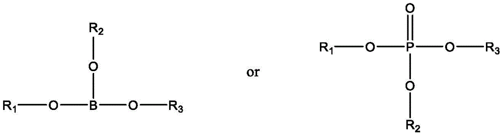
其中,in,
R1,R2,R3分别独立地选自:H,D,具有1至20个C原子的直链烷基、烷氧基或硫代烷氧基基团,具有3至20个C原子的支链或环状的烷基、烷氧基或硫代烷氧基基团,甲硅烷基基团,具有1至20个C原子的取代的酮基基团,具有2至20个C原子的烷氧基羰基基团,具有7至20个C原子的芳氧基羰基基团,氰基基团,氨基甲酰基基团,卤甲酰基基团,甲酰基基团,异氰基基团,异氰酸酯基团,硫氰酸酯基团或异硫氰酸酯基团,羟基基团,硝基基团,CF3基团,Cl,Br,F,具有5至40个环原子的取代或未取代的芳族或杂芳族环系,具有5至40个环原子的芳氧基或杂芳氧基基团,或其组合,所述无机酯溶剂的沸点≥150℃,所述无机酯溶剂能够从溶剂体系中蒸发,以形成功能材料薄膜。R 1 , R 2 , R 3 are each independently selected from: H, D, a straight-chain alkyl, alkoxy or thioalkoxy group having 1 to 20 C atoms, having 3 to 20 C atoms branched or cyclic alkyl, alkoxy or thioalkoxy groups, silyl groups, substituted keto groups with 1 to 20 C atoms, with 2 to 20 C atoms alkoxycarbonyl groups, aryloxycarbonyl groups with 7 to 20 C atoms, cyano groups, carbamoyl groups, haloformyl groups, formyl groups, isocyano groups , isocyanate group, thiocyanate group or isothiocyanate group, hydroxyl group, nitro group, CF3 group, Cl, Br, F, substituted with 5 to 40 ring atoms or Unsubstituted aromatic or heteroaromatic ring systems, aryloxy or heteroaryloxy groups having 5 to 40 ring atoms, or combinations thereof, the inorganic ester solvent has a boiling point ≥ 150°C, the inorganic ester The solvent can be evaporated from the solvent system to form a thin film of functional material.
在本发明的一些优选实施例中,所述无机酯溶剂在25℃的粘度在1cPs到100cPs范围内。In some preferred embodiments of the present invention, the viscosity of the inorganic ester solvent at 25°C is in the range of 1 cPs to 100 cPs.
在本发明的一些优选实施例中,所述无机酯溶剂在25℃的表面张力在19dyne/cm到50dyne/cm范围内。In some preferred embodiments of the present invention, the surface tension of the inorganic ester solvent at 25°C is in the range of 19 dyne/cm to 50 dyne/cm.
在本发明的一些优选实施例中,所述无机酯溶剂选自硼酸烷酯或磷酸烷酯。In some preferred embodiments of the present invention, the inorganic ester solvent is selected from alkyl borate or alkyl phosphate.
在本发明的一些优选实施例中,所述无机酯溶剂选自:硼酸三丁酯、硼酸三戊酯、磷酸三甲酯、磷酸三乙酯、磷酸三丁酯、磷酸三(2-乙基己基)酯、磷酸三苯酯、磷酸二乙酯、磷酸二丁酯、磷酸二(2-乙基己基)酯或其混合物。In some preferred embodiments of the present invention, the inorganic ester solvent is selected from the group consisting of: tributyl borate, tripentyl borate, trimethyl phosphate, triethyl phosphate, tributyl phosphate, tris(2-ethyl phosphate) hexyl) ester, triphenyl phosphate, diethyl phosphate, dibutyl phosphate, bis(2-ethylhexyl) phosphate or mixtures thereof.
在本发明的一些优选实施例中,进一步包含至少一种其它溶剂,且所述无机酯溶剂占混合溶剂总重量的50%以上。In some preferred embodiments of the present invention, at least one other solvent is further included, and the inorganic ester solvent accounts for more than 50% of the total weight of the mixed solvent.
在本发明的一些优选实施例中,所述功能材料是无机纳米材料。In some preferred embodiments of the present invention, the functional material is an inorganic nanomaterial.
在本发明的一些优选实施例中,所述功能材料是量子点材料,即其粒径具有单分散的尺寸分布,其形状可选自球形、立方体、棒状或支化结构的不同纳米形貌。In some preferred embodiments of the present invention, the functional material is a quantum dot material, that is, its particle size has a monodisperse size distribution, and its shape can be selected from different nano-morphologies of spherical, cubic, rod-like or branched structures.
在本发明的一些优选实施例中,所述功能材料是发光量子点材料,其发光波长位于380nm~2500nm之间。In some preferred embodiments of the present invention, the functional material is a light-emitting quantum dot material, and its light-emitting wavelength is between 380 nm and 2500 nm.
在本发明的一些优选实施例中,进一步包含无机功能材料,选自元素周期表IV族、II-VI族、II-V族、III-V族、III-VI族、IV-VI族、I-III-VI族、II-IV-VI族、II-IV-V族二元或多元半导体化合物或其混合物。In some preferred embodiments of the present invention, it further comprises inorganic functional materials selected from Group IV, Group II-VI, Group II-V, Group III-V, Group III-VI, Group IV-VI, and Group I of the Periodic Table of Elements - Group III-VI, II-IV-VI, II-IV-V binary or multiple semiconductor compounds or mixtures thereof.
在本发明的一些优选实施例中,所述功能材料是钙钛矿纳米粒子材料。In some preferred embodiments of the present invention, the functional material is a perovskite nanoparticle material.
在本发明的一些优选实施例中,所述功能材料是发光钙钛矿纳米材料、或金属纳米粒子材料、或金属氧化物纳米粒子材料,或其混合物。In some preferred embodiments of the present invention, the functional material is a luminescent perovskite nanomaterial, or a metal nanoparticle material, or a metal oxide nanoparticle material, or a mixture thereof.
在本发明的一些优选实施例中,所述功能材料是有机功能材料。In some preferred embodiments of the present invention, the functional material is an organic functional material.
在本发明的一些优选实施例中,所述有机功能材料选自空穴注入材料,空穴传输材料,电子传输材料,电子注入材料,电子阻挡材料,空穴阻挡材料,发光体,或主体材料。In some preferred embodiments of the present invention, the organic functional material is selected from hole injection materials, hole transport materials, electron transport materials, electron injection materials, electron blocking materials, hole blocking materials, light emitters, or host materials .
在本发明的一些优选实施例中,所述有机功能材料包含至少一种主体材料和至少一种发光体。In some preferred embodiments of the present invention, the organic functional material comprises at least one host material and at least one emitter.
在本发明的一些优选实施例中,所述功能材料的重量百分比为0.3%~30%,所述无机酯溶剂的重量百分比为70%~99.7%。In some preferred embodiments of the present invention, the weight percentage of the functional material is 0.3% to 30%, and the weight percentage of the inorganic ester solvent is 70% to 99.7%.
本发明另一个目的还在于提供一种电子器件,其包含功能层,该功能层由如上所述的印刷组合物印刷或涂布而成,所述无机酯溶剂能够从溶剂体系中蒸发,以形成功能材料薄膜。Another object of the present invention is to provide an electronic device comprising a functional layer printed or coated from the printing composition as described above, wherein the inorganic ester solvent can be evaporated from the solvent system to form Functional material films.
在本发明的一些优选实施例中,所述电子器件可选自量子点发光二极管、量子点光伏电池、量子点发光电池、量子点场效应管、量子点发光场效应管、量子点激光器、量子点传感器、有机发光二极管、有机光伏电池、有机发光电池、有机场效应管、有机发光场效应管、有机激光器或有机传感器。In some preferred embodiments of the present invention, the electronic device may be selected from quantum dot light-emitting diodes, quantum dot photovoltaic cells, quantum dot light-emitting cells, quantum dot field effect transistors, quantum dot light emitting field effect tubes, quantum dot lasers, quantum dot Point sensors, organic light emitting diodes, organic photovoltaic cells, organic light emitting cells, organic field effect transistors, organic light emitting field effect transistors, organic lasers or organic sensors.
本发明的另一个目的还在于提供一种功能材料薄膜的制备方法,其中将如上所述的印刷组合物用印刷或涂布的方法涂布于一基板上,其中所述印刷或涂布的方法可选自:喷墨打印,喷印,活版印刷,丝网印刷,浸涂,旋转涂布,刮刀涂布,辊筒印花,扭转辊印刷,平版印刷,柔版印刷,轮转印刷,喷涂,刷涂或移印,或狭缝型挤压式涂布。Another object of the present invention is to provide a method for preparing a functional material film, wherein the printing composition as described above is coated on a substrate by a method of printing or coating, wherein the method of printing or coating Can be selected from: inkjet printing, jet printing, letterpress printing, screen printing, dip coating, spin coating, blade coating, roll printing, twist roll printing, offset printing, flexographic printing, rotary printing, spray coating, brushing Coating or pad printing, or slot extrusion coating.
有益效果:Beneficial effects:
本发明提供一种印刷组合物,其可以将粘度和表面张力,按照特定的印刷方法,特别是喷墨印刷,调节到合适的范围便于打印,并形成表面均匀的薄膜。同时溶剂可以通过后处理有效移除,如热处理或真空处理,有利于保证电子器件的性能。因此本发明提供了一种用于制备高质量功能薄膜的油墨,特别是包含量子点和有机半导体材料的印刷油墨,为可印刷电子或光电子器件提供了技术解决方案。The present invention provides a printing composition, which can adjust the viscosity and surface tension to a suitable range according to a specific printing method, especially ink jet printing, to facilitate printing and form a film with a uniform surface. At the same time, the solvent can be effectively removed by post-processing, such as heat treatment or vacuum treatment, which is beneficial to ensure the performance of electronic devices. Therefore, the present invention provides an ink for preparing high-quality functional thin films, especially a printing ink containing quantum dots and organic semiconductor materials, which provides a technical solution for printable electronic or optoelectronic devices.
附图说明:Description of drawings:
图1是按照本发明的一种优选的发光器件结构图,图中101是基板,102是阳极,103是空穴注入层(HIL)或空穴传输层(HTL),104是发光层(电致发光器件)或光吸收层(光伏电池),105是电子注入层(EIL)或电子传输层(ETL),106是阴极。1 is a structural diagram of a preferred light-emitting device according to the present invention, in which 101 is a substrate, 102 is an anode, 103 is a hole injection layer (HIL) or a hole transport layer (HTL), and 104 is a light-emitting layer (electrical luminescent device) or light absorbing layer (photovoltaic cell), 105 is the electron injection layer (EIL) or electron transport layer (ETL), 106 is the cathode.
具体实施方式:Detailed ways:
本发明提供一种印刷组合物,提供的组合物包含至少一种功能材料及至少一种无机酯溶剂。在某些优选的实施例中,所述的无机酯溶剂在25℃的粘度,在1cPs到100cPs范围,其在25℃的表面张力,在19dyne/cm到50dyne/cm范围,其沸点高于150℃。本发明还涉及包含该印刷组合物的电子器件及功能材料薄膜的制备方法。The present invention provides a printing composition comprising at least one functional material and at least one inorganic ester solvent. In certain preferred embodiments, the viscosity of the inorganic ester solvent at 25°C ranges from 1 cPs to 100 cPs, its surface tension at 25°C ranges from 19 dyne/cm to 50 dyne/cm, and its boiling point is higher than 150 °C. The present invention also relates to a method for preparing an electronic device and a functional material film comprising the printing composition.
为使本发明的目的、技术方案及效果更加清楚、明确,以下对本发明进一步详细说明。应当理解,此处所描述的详细说明和具体实施例仅仅用以解释本发明,并不用于限定本发明。In order to make the objectives, technical solutions and effects of the present invention clearer and clearer, the present invention will be described in further detail below. It should be understood that the detailed description and specific embodiments described herein are only for explaining the present invention, and not for limiting the present invention.
在本发明中,印刷组合物、印刷油墨、油墨具有相同的含义,它们之间可以互换。In the present invention, printing compositions, printing inks, and inks have the same meaning and are interchangeable among them.
本发明提供一种印刷组合物,包含至少一种功能材料和至少一种具有如下通式所示的无机酯溶剂:The present invention provides a printing composition comprising at least one functional material and at least one inorganic ester solvent having the following general formula:

其中,in,
R1,R2,R3分别任选地为H,或D,或具有1至20个C原子的直链烷基、烷氧基或硫代烷氧基基团,或者具有3至20个C原子的支链或环状的烷基、烷氧基或硫代烷氧基基团或者是甲硅烷基基团,或具有1至20个C原子的取代的酮基基团,或具有2至20个C原子的烷氧基羰基基团,或具有7至20个C原子的芳氧基羰基基团,氰基基团(-CN),氨基甲酰基基团(-C(=O)NH2),卤甲酰基基团(-C(=O)-X其中X代表卤素原子),甲酰基基团(-C(=O)-H),异氰基基团,异氰酸酯基团,硫氰酸酯基团或异硫氰酸酯基团,羟基基团,硝基基团,CF3基团,Cl,Br,F,可交联的基团或者具有5至40个环原子的取代或未取代的芳族或杂芳族环系,或具有5至40个环原子的芳氧基或杂芳氧基基团,或这些体系的组合。R 1 , R 2 , R 3 are each optionally H, or D, or a straight-chain alkyl, alkoxy or thioalkoxy group having 1 to 20 C atoms, or 3 to 20 A branched or cyclic alkyl, alkoxy or thioalkoxy group of C atoms is either a silyl group, or a substituted keto group having 1 to 20 C atoms, or a 2 alkoxycarbonyl groups of to 20 C atoms, or aryloxycarbonyl groups of 7 to 20 C atoms, cyano groups (-CN), carbamoyl groups (-C(=O) NH 2 ), haloformyl group (-C(=O)-X where X represents a halogen atom), formyl group (-C(=O)-H), isocyano group, isocyanate group, Thiocyanate groups or isothiocyanate groups, hydroxyl groups, nitro groups, CF3 groups, Cl, Br, F, crosslinkable groups or groups with 5 to 40 ring atoms A substituted or unsubstituted aromatic or heteroaromatic ring system, or an aryloxy or heteroaryloxy group having from 5 to 40 ring atoms, or a combination of these systems.
在一些优选的实施例中,R1,R2,R3分别任选地为H,或D,或具有1至10个C原子的直链烷基、烷氧基或硫代烷氧基基团,或者具有3至10个C原子的支链或环状的烷基、烷氧基或硫代烷氧基基团或者是甲硅烷基基团,或具有1至10个C原子的取代的酮基基团,或具有2至10个C原子的烷氧基羰基基团,或具有7至10个C原子的芳氧基羰基基团,氰基基团(-CN),氨基甲酰基基团(-C(=O)NH2),卤甲酰基基团(-C(=O)-X其中X代表卤素原子),甲酰基基团(-C(=O)-H),异氰基基团,异氰酸酯基团,硫氰酸酯基团或异硫氰酸酯基团,羟基基团,硝基基团,CF3基团,Cl,Br,F,可交联的基团或者具有5至20个环原子的取代或未取代的芳族或杂芳族环系,或具有5至20个环原子的芳氧基或杂芳氧基基团,或这些体系的组合。In some preferred embodiments, R 1 , R 2 , R 3 are each optionally H, or D, or a straight-chain alkyl, alkoxy, or thioalkoxy group having 1 to 10 C atoms group, or a branched or cyclic alkyl, alkoxy or thioalkoxy group having 3 to 10 C atoms or a silyl group, or a substituted 1 to 10 C atom Keto group, or alkoxycarbonyl group with 2 to 10 C atoms, or aryloxycarbonyl group with 7 to 10 C atoms, cyano group (-CN), carbamoyl group group (-C(=O) NH2 ), haloformyl group (-C(=O)-X where X represents a halogen atom), formyl group (-C(=O)-H), isocyanide groups, isocyanate groups, thiocyanate groups or isothiocyanate groups, hydroxyl groups, nitro groups, CF 3 groups, Cl, Br, F, crosslinkable groups or A substituted or unsubstituted aromatic or heteroaromatic ring system having 5 to 20 ring atoms, or an aryloxy or heteroaryloxy group having 5 to 20 ring atoms, or a combination of these systems.
按照本发明的印刷组合物,包含的无机酯溶剂其沸点≥150℃。所述的无机酯溶剂可从溶剂体系中蒸发,以形成功能材料的薄膜。According to the printing composition of the present invention, the inorganic ester solvent contained has a boiling point of ≥150°C. The inorganic ester solvent can be evaporated from the solvent system to form thin films of functional materials.
用于溶解功能材料的基于无机酯的溶剂在选取时需考虑其沸点参数。在某些实施例中,所述的基于无机酯的有机溶剂的沸点≥180℃;在某些优选的实施例中,所述的基于无机酯的溶剂其沸点≥200℃或220℃;在某些实施例中,所述的基于无机酯的溶剂其沸点≥250℃;在另一些优选实施例中,所述的基于无机酯的溶剂其沸点≥275℃或≥300℃。这些范围内的沸点对防止喷墨印刷头的喷嘴堵塞是有益的。所述的基于无机酯的溶剂可从溶剂体系中蒸发,以形成包含功能材料薄膜。Inorganic ester-based solvents for dissolving functional materials should be selected considering their boiling point parameters. In certain embodiments, the boiling point of the inorganic ester-based organic solvent is greater than or equal to 180°C; in certain preferred embodiments, the boiling point of the inorganic ester-based solvent is greater than or equal to 200°C or 220°C; In some embodiments, the boiling point of the inorganic ester-based solvent is ≥250°C; in other preferred embodiments, the boiling point of the inorganic ester-based solvent is ≥275°C or ≥300°C. Boiling points within these ranges are beneficial for preventing nozzle clogging of ink jet print heads. The inorganic ester-based solvent can be evaporated from the solvent system to form a thin film containing functional materials.
按照本发明的印刷组合物,包含至少一种无机酯溶剂,且所述的无机酯溶剂在25℃的粘度,在1cPs到100cPs范围。The printing composition according to the present invention comprises at least one inorganic ester solvent, and the viscosity of the inorganic ester solvent at 25° C. is in the range of 1 cPs to 100 cPs.
用于溶解功能材料的基于无机酯的溶剂在选取时需考虑其油墨的粘度参数。粘度可以通过不同的方法调节,如通过合适的溶剂选取和油墨中功能材料的浓度。按照本发明的包含基于无机酯溶剂的溶剂体系可方便人们将印刷油墨按照所用的印刷方法在适当的范围调节。一般地,按照本发明的印刷组合物包含的功能材料的重量比为0.3%~30wt%范围,较好的为0.5%~20wt%范围,更好的为0.5%~15wt%范围,最好的为0.5%~10wt%范围。在一个优选的实施例中,所述的基于无机酯的溶剂的粘度低于100cps;在一个更为优选的实施例中,所述的基于无机酯的溶剂的粘度低于50cps;在一个最为优选的实施例中,所述的基于无机酯的溶剂的粘度为1.5到20cps。这里的粘度是指在印刷时的环境温度下的粘度,一般在15-30℃,较好的是18-28℃,更好是20-25℃,最好是23-25℃。如此配制的印刷组合物将特别适合于喷墨印刷。Inorganic ester-based solvents for dissolving functional materials should be selected considering the viscosity parameters of their inks. The viscosity can be adjusted by different methods, such as by suitable solvent selection and concentration of functional materials in the ink. The solvent system comprising the inorganic ester-based solvent according to the present invention allows one to adjust the printing ink within an appropriate range according to the printing method used. Generally, the weight ratio of the functional material contained in the printing composition according to the present invention is in the range of 0.3% to 30% by weight, preferably in the range of 0.5% to 20% by weight, more preferably in the range of 0.5% to 15% by weight, and most preferably in the range of 0.5% to 20% by weight. It is in the range of 0.5% to 10% by weight. In a preferred embodiment, the viscosity of the inorganic ester-based solvent is lower than 100cps; in a more preferred embodiment, the viscosity of the inorganic ester-based solvent is lower than 50cps; in a most preferred embodiment In the examples of , the viscosity of the inorganic ester-based solvent is 1.5 to 20 cps. The viscosity here refers to the viscosity at the ambient temperature during printing, which is generally 15-30°C, preferably 18-28°C, more preferably 20-25°C, and most preferably 23-25°C. Printing compositions so formulated would be particularly suitable for ink jet printing.
在一个优选的实施例中,按照本发明的印刷组合物,当其按照如上配比配制后,在25℃下的粘度约在1cps到100cps范围;更好是在1cps到50cps范围;最好是在1.5cps到20cps范围。In a preferred embodiment, the printing composition according to the present invention, when formulated according to the above formula, has a viscosity at 25° C. in the range of about 1 cps to 100 cps; more preferably in the range of 1 cps to 50 cps; In the 1.5cps to 20cps range.
按照本发明的印刷组合物,包含至少一种无机酯溶剂,且所述的无机酯溶剂在25℃的表面张力,在19dyne/cm到50dyne/cm范围。The printing composition according to the present invention comprises at least one inorganic ester solvent, and the surface tension of the inorganic ester solvent at 25° C. is in the range of 19 dyne/cm to 50 dyne/cm.
用于溶解功能材料的基于无机酯的溶剂在选取时需考虑其表面张力参数。合适的油墨表面张力参数需要适合于特定的基板和特定的印刷方法。例如对喷墨印刷,在一个优选的实施例中,所述的基于无机酯的溶剂在25℃下的表面张力约在19dyne/cm到50dyne/cm范围;在一个更为优选的实施例中,所述的基于无机酯的溶剂在25℃下的表面张力约在22dyne/cm到35dyne/cm范围;在一个最为优选的实施例中,所述的基于无机酯的溶剂在25℃下的表面张力约在25dyne/cm到33dyne/cm范围。Inorganic ester-based solvents for dissolving functional materials should be selected considering their surface tension parameters. Appropriate ink surface tension parameters need to be suitable for a specific substrate and a specific printing method. For example, for inkjet printing, in a preferred embodiment, the surface tension of the inorganic ester-based solvent at 25°C is in the range of about 19 dyne/cm to 50 dyne/cm; in a more preferred embodiment, The surface tension of the inorganic ester-based solvent at 25° C. is in the range of about 22 dyne/cm to 35 dyne/cm; in a most preferred embodiment, the surface tension of the inorganic ester-based solvent at 25° C. About 25dyne/cm to 33dyne/cm range.
在一个优选的实施例中,按照本发明的印刷组合物在25℃下的表面张力约在19dyne/cm到50dyne/cm范围;更好是在22dyne/cm到35dyne/cm范围;最好是在25dyne/cm到33dyne/cm范围。In a preferred embodiment, the printing composition according to the present invention has a surface tension at 25°C in the range of about 19 dyne/cm to 50 dyne/cm; more preferably in the range of 22 dyne/cm to 35 dyne/cm; 25dyne/cm to 33dyne/cm range.
满足上述沸点及表面张力参数及粘度参数的基于无机酯的溶剂体系获得的油墨能够形成具有均匀厚度及组成性质的功能材料薄膜。The ink obtained from the inorganic ester-based solvent system satisfying the above-mentioned boiling point and surface tension parameters and viscosity parameters can form functional material films with uniform thickness and compositional properties.
在一些优选的实施例中,按照本发明的印刷组合物,所包含的无机酯溶剂选自硼酸烷酯和磷酸烷酯。In some preferred embodiments, according to the printing composition of the present invention, the included inorganic ester solvent is selected from the group consisting of alkyl borate and alkyl phosphate.
适合本发明的无机酯溶剂可选自但不限制于:硼酸三丁酯、硼酸三戊酯、磷酸三甲酯、磷酸三乙酯、磷酸三丁酯、磷酸三(2-乙基己基)酯、磷酸三苯酯、磷酸二乙酯、磷酸二丁酯、磷酸二(2-乙基己基)酯等。Inorganic ester solvents suitable for the present invention may be selected from, but not limited to, tributyl borate, tripentyl borate, trimethyl phosphate, triethyl phosphate, tributyl phosphate, tris(2-ethylhexyl) phosphate , Triphenyl phosphate, diethyl phosphate, dibutyl phosphate, bis(2-ethylhexyl) phosphate, etc.
在一些优选的实施例中,本发明涉及的印刷组合物包含单一的基于无机酯的溶剂。所述的单一的基于无机酯的溶剂可优选选自硼酸三丁酯,硼酸三戊酯,磷酸三乙酯,和磷酸三苯酯。In some preferred embodiments, the printing compositions contemplated by the present invention comprise a single inorganic ester-based solvent. The single inorganic ester-based solvent may preferably be selected from tributyl borate, tripentyl borate, triethyl phosphate, and triphenyl phosphate.
在另一些优选的实施例中,本发明涉及的印刷组合物包含两种及两种以上的基于无机酯溶剂的混合物。In other preferred embodiments, the printing composition involved in the present invention comprises a mixture of two or more inorganic ester-based solvents.
在一些优选的实施方案中,本发明涉及的印刷组合物包含的无机酯溶剂是磷酸三苯酯和磷酸三乙酯的混合物,且磷酸三苯酯占混合溶剂总重量的50%以上,较优是70%以上,最优是90%以上。In some preferred embodiments, the inorganic ester solvent contained in the printing composition of the present invention is a mixture of triphenyl phosphate and triethyl phosphate, and triphenyl phosphate accounts for more than 50% of the total weight of the mixed solvent, preferably It is more than 70%, and the most optimal is more than 90%.
在另一些优选的实施方案中,本发明涉及的印刷组合物包含的无机酯溶剂是磷酸三苯酯和硼酸三戊酯的混合物,且磷酸三苯酯占混合溶剂总重量的50%以上,较优是70%以上,最优是90%以上。In some other preferred embodiments, the inorganic ester solvent contained in the printing composition of the present invention is a mixture of triphenyl phosphate and tripentyl borate, and triphenyl phosphate accounts for more than 50% of the total weight of the mixed solvent, more than The best is 70% or more, and the best is 90% or more.
在某些实施例中,按照本发明的一种印刷组合物,进一步包含至少另一种有机溶剂,其中无机酯溶剂占混合溶剂总重量的50%以上。优选地,包含的无机酯溶剂占溶剂总重量的至少70%;更优地,包含的无机酯溶剂占溶剂总重量的至少80%。最优地,所述的基于无机酯的溶剂体系包含至少90%重量比的无机酯溶剂,或基本上由无机酯溶剂组成,或完全由无机酯溶剂组成。In certain embodiments, a printing composition according to the present invention further comprises at least another organic solvent, wherein the inorganic ester solvent accounts for more than 50% of the total weight of the mixed solvent. Preferably, the inorganic ester solvent is included at least 70% by weight of the total solvent; more preferably, the inorganic ester solvent is included at least 80% by weight of the total solvent. Optimally, the inorganic ester-based solvent system comprises at least 90% by weight of the inorganic ester solvent, or consists essentially of the inorganic ester solvent, or consists entirely of the inorganic ester solvent.
在一些优选的实施方案中,上述的另一种有机溶剂选自芳族或杂芳族溶剂,或基于醇基或醚基或酮基或酯基或醛基的溶剂。In some preferred embodiments, the other organic solvent mentioned above is selected from aromatic or heteroaromatic solvents, or solvents based on alcohol or ether or ketone or ester or aldehyde groups.
在另一些优选的实施方案中,上述的另一种有机溶剂的例子,包括(但不限于):甲醇、乙醇、2-甲氧基乙醇、二氯甲烷、三氯甲烷、氯苯、邻二氯苯、四氢呋喃、苯甲醚、吗啉、甲苯、邻二甲苯、间二甲苯、对二甲苯、1,4二氧杂环己烷、丙酮、甲基乙基酮、1,2二氯乙烷、3-苯氧基甲苯、1,1,1-三氯乙烷、1,1,2,2-四氯乙烷、醋酸乙酯、醋酸丁酯、二甲基甲酰胺、二甲基乙酰胺、二甲基亚砜、四氢萘、萘烷、茚和/或它们的混合物。In other preferred embodiments, examples of the above-mentioned another organic solvent include (but are not limited to): methanol, ethanol, 2-methoxyethanol, dichloromethane, chloroform, chlorobenzene, o-dichloromethane Chlorobenzene, tetrahydrofuran, anisole, morpholine, toluene, ortho-xylene, meta-xylene, para-xylene, 1,4 dioxane, acetone, methyl ethyl ketone, 1,2 dichloroethyl Alkane, 3-phenoxytoluene, 1,1,1-trichloroethane, 1,1,2,2-tetrachloroethane, ethyl acetate, butyl acetate, dimethylformamide, dimethyl Acetamide, dimethyl sulfoxide, tetralin, decalin, indene and/or mixtures thereof.
按照本发明所述的基于无机酯的溶剂体系能够有效地溶解功能材料,即作为新的溶剂取代传统使用的溶解功能材料的溶剂,如甲苯、二甲苯、氯仿、氯苯、二氯苯、正庚烷等。The inorganic ester-based solvent system according to the present invention can effectively dissolve functional materials, that is, as a new solvent to replace the traditionally used solvents for dissolving functional materials, such as toluene, xylene, chloroform, chlorobenzene, dichlorobenzene, normal Heptane etc.
所述的印刷油墨还可以另外包括一个或多个组份,例如表面活性化合物,润滑剂,润湿剂,分散剂,疏水剂,粘接剂等,用于调节粘度,成膜性能,提高附着性等。The printing ink may additionally include one or more components, such as surface active compounds, lubricants, wetting agents, dispersing agents, hydrophobic agents, adhesives, etc., for adjusting viscosity, film-forming properties, and improving adhesion. sex, etc.
按照本发明的印刷油墨可以通过多种技术沉积得到功能薄膜,适合的印刷或涂布技术包括(但不限于)喷墨打印,喷印(Nozzle Printing),活版印刷,丝网印刷,浸涂,旋转涂布,刮刀涂布,辊筒印花,扭转辊印刷,平版印刷,柔版印刷,轮转印刷,喷涂,刷涂或移印,狭缝型挤压式涂布等。优选的打印技术是喷墨印刷,喷印及凹版印刷。有关打印技术,及其对有关油墨的相关要求,如溶剂及浓度,粘度等,的详细信息请参见Helmut Kipphan主编的《印刷媒体手册:技术和生产方法》(Handbook of Print Media:Technologies andProduction Methods),ISBN 3-540-67326-1。一般地,不同的打印技术对所采用的油墨有不同的特性要求。例如,适用于喷墨打印的印刷油墨,需要对油墨的表面张力、粘度、及浸润性进行调控,使得油墨在印刷温度下(比如室温,25℃)能够很好地经由喷嘴喷出而不至于干燥于喷嘴上或堵塞喷嘴,或能在特定的基板上形成连续、平整和无缺陷的薄膜。The printing ink according to the present invention can be deposited by various techniques to obtain functional films. Suitable printing or coating techniques include (but are not limited to) ink jet printing, jet printing (Nozzle Printing), letterpress printing, screen printing, dip coating, Spin coating, blade coating, roll printing, twist roll printing, offset printing, flexographic printing, rotary printing, spray coating, brush coating or pad printing, slot extrusion coating, etc. Preferred printing techniques are ink jet printing, jet printing and gravure printing. For detailed information on printing technology and its related requirements for inks, such as solvent and concentration, viscosity, etc., please refer to the "Handbook of Print Media: Technologies and Production Methods" edited by Helmut Kipphan (Handbook of Print Media: Technologies and Production Methods) , ISBN 3-540-67326-1. Generally, different printing technologies have different requirements on the characteristics of the inks used. For example, for printing inks suitable for inkjet printing, it is necessary to adjust the surface tension, viscosity, and wettability of the ink, so that the ink can be well ejected through the nozzle at the printing temperature (such as room temperature, 25°C) without causing Dry on the nozzle or plug the nozzle, or can form a continuous, flat and defect-free film on a specific substrate.
按照本发明的印刷组合物包含至少一种功能材料。The printing composition according to the present invention comprises at least one functional material.
在本发明中,功能材料优选是指具有某些光电功能的材料。光电功能包括,但不限于,空穴注入功能,空穴传输功能,电子传输功能,电子注入功能,电子阻挡功能,空穴阻挡功能,发光功能,主体功能。相应的功能材料被称为空穴注入材料(HIM),空穴传输材料(HTM),电子传输材料(ETM),电子注入材料(EIM),电子阻挡材料(EBM),空穴阻挡材料(HBM),发光体(Emitter),主体材料(Host)。In the present invention, the functional material preferably refers to a material having some optoelectronic function. Optoelectronic functions include, but are not limited to, hole injection function, hole transport function, electron transport function, electron injection function, electron blocking function, hole blocking function, light emitting function, host function. The corresponding functional materials are called hole injection material (HIM), hole transport material (HTM), electron transport material (ETM), electron injection material (EIM), electron blocking material (EBM), hole blocking material (HBM) ), Emitter, Host.
功能材料可以是有机材料或无机材料。Functional materials can be organic materials or inorganic materials.
在一个优选的实施方案中,按照本发明的印刷组合物包含的至少一种功能材料是无机纳米材料。In a preferred embodiment, the at least one functional material comprised in the printing composition according to the present invention is an inorganic nanomaterial.
优选的,所述的印刷组合物中,所述的至少一种无机纳米材料是无机半导体纳米粒子材料。Preferably, in the printing composition, the at least one inorganic nanomaterial is an inorganic semiconductor nanoparticle material.
本发明中,无机纳米材料的平均粒径约在1到1000nm范围内。在某些优选的实施例中,无机纳米材料的平均粒径约在1到100nm。在某些更为优选的实施例中,无机纳米材料的平均粒径约在1到20nm,最好在1到10nm。In the present invention, the average particle size of the inorganic nanomaterial is in the range of about 1 to 1000 nm. In certain preferred embodiments, the average particle size of the inorganic nanomaterials is about 1 to 100 nm. In some more preferred embodiments, the average particle size of the inorganic nanomaterials is about 1 to 20 nm, preferably 1 to 10 nm.
所述的无机纳米材料可以选自不同的形状,包含但不限于球形、立方体、棒状、盘形或支化结构等不同纳米形貌,以及各种形状颗粒的混合物。The inorganic nanomaterials can be selected from different shapes, including but not limited to spherical, cubic, rod-shaped, disc-shaped or branched structures and other nano-morphologies, as well as mixtures of particles of various shapes.
在一个优选的实施例中,所述的无机纳米材料是量子点材料,具有非常狭窄的、单分散的尺寸分布,即颗粒与颗粒之间的尺寸差异非常小。优选地,单分散的量子点在尺寸上的偏差均方根小于15%rms;更优地,单分散的量子点在尺寸上的偏差均方根小于10%rms;最优地,单分散的量子点在尺寸上的偏差均方根小于5%rms。In a preferred embodiment, the inorganic nanomaterial is a quantum dot material with a very narrow, monodisperse size distribution, that is, the particle-to-particle size difference is very small. Preferably, monodisperse quantum dots have a rms deviation in size of less than 15% rms; more preferably, monodisperse quantum dots have a rms deviation in size of less than 10% rms; The rms deviation of quantum dots in size is less than 5% rms.
在一个优选的实施例中,所述的无机纳米材料是发光材料。In a preferred embodiment, the inorganic nanomaterial is a luminescent material.
在一个更加优选的实施例中,所述的发光无机纳米材料是量子点发光材料。In a more preferred embodiment, the light-emitting inorganic nanomaterial is a quantum dot light-emitting material.
一般地,发光量子点可以在波长380纳米到2500纳米之间发光。例如,已发现,具有CdS核的量子点的发光波长位于约400纳米到560纳米范围;具有CdSe核的量子点的发光波长位于约490纳米到620纳米范围;具有CdTe核的量子点的发光波长位于约620纳米到680纳米范围;具有InGaP核的量子点的发光波长位于约600纳米到700纳米范围;具有PbS核的量子点的发光波长位于约800纳米到2500纳米范围;具有PbSe核的量子点的发光波长位于约1200纳米到2500纳米范围;具有CuInGaS核的量子点的发光波长位于约600纳米到680纳米范围;具有ZnCuInGaS核的量子点的发光波长位于约500纳米到620纳米范围;具有CuInGaSe核的量子点的发光波长位于约700纳米到1000纳米范围;Generally, light-emitting quantum dots can emit light at wavelengths between 380 nanometers and 2500 nanometers. For example, it has been found that the emission wavelengths of quantum dots with CdS cores lie in the range of about 400 nanometers to 560 nanometers; the emission wavelengths of quantum dots with CdSe cores are in the range of about 490 nanometers to 620 nanometers; the emission wavelengths of quantum dots with CdTe cores In the range of about 620 nanometers to 680 nanometers; the emission wavelengths of quantum dots with InGaP cores are in the range of about 600 nanometers to 700 nanometers; the emission wavelengths of quantum dots with PbS cores are in the range of about 800 nanometers to 2500 nanometers; quantum dots with PbSe cores The emission wavelength of the dot is in the range of about 1200 nanometers to 2500 nanometers; the emission wavelength of quantum dots with CuInGaS core is in the range of about 600 nanometers to 680 nanometers; the emission wavelength of quantum dots with ZnCuInGaS core is in the range of about 500 nanometers to 620 nanometers; The emission wavelength of the quantum dots of the CuInGaSe core lies in the range of about 700 nanometers to 1000 nanometers;
在一个优选的实施例中,所述的量子点材料包含至少一种能够发出发光峰值波长位于450nm~460nm的蓝光、或发光峰值波长位于520nm~540nm的绿光、或发光峰值波长位于615nm~630nm的红光,或它们的混合物。In a preferred embodiment, the quantum dot material comprises at least one type of blue light that can emit light with a peak wavelength of 450 nm to 460 nm, or green light with a peak wavelength of luminescence of 520 nm to 540 nm, or a peak wavelength of luminescence of 615 nm to 630 nm. of red light, or a mixture thereof.
所包含的量子点可以选自特殊的化学组成、形貌结构和/或大小尺寸,以获得在电刺激下发出所需波长的光。关于量子点的发光性质与其化学组成、形貌结构和/或大小尺寸的关系可以参见Annual Review of Material Sci.,2000,30,545-610;OpticalMaterials Express.,2012,2,594-628;Nano Res,2009,2,425-447。特此将上述列出的专利文件中的全部内容并入本文作为参考。The included quantum dots can be selected from specific chemical compositions, topographical structures and/or sizes to obtain light of desired wavelengths under electrical stimulation. For the relationship between the luminescence properties of quantum dots and their chemical composition, morphology and/or size, please refer to Annual Review of Material Sci., 2000, 30, 545-610; Optical Materials Express., 2012, 2, 594-628; Nano Res, 2009, 2,425-447. The entire contents of the above-listed patent documents are hereby incorporated by reference.
量子点的窄的粒径分布能使量子点具有更窄的发光光谱(J.Am.Chem.Soc.,1993,115,8706;US 20150108405)。此外,根据所采用的化学组成和结构的不同,量子点的尺寸需在上述的尺寸范围内做相应调节,以获得所需波长的发光性质。The narrow particle size distribution of quantum dots enables quantum dots to have narrower emission spectra (J.Am.Chem.Soc., 1993, 115, 8706; US 20150108405). In addition, according to the different chemical compositions and structures used, the size of the quantum dots needs to be adjusted within the above-mentioned size range to obtain the luminescence properties of the desired wavelengths.
优选地,发光量子点是半导体纳米晶体。一般地,半导体纳米晶体的尺寸为约2纳米到约15纳米的范围内。此外,根据所采用的化学组成和结构的不同,量子点的尺寸需在上述的尺寸范围内做相应调节,以获得所需波长的发光性质。Preferably, the luminescent quantum dots are semiconductor nanocrystals. Generally, the size of the semiconductor nanocrystals is in the range of about 2 nanometers to about 15 nanometers. In addition, according to the different chemical compositions and structures used, the size of the quantum dots needs to be adjusted within the above-mentioned size range to obtain the luminescence properties of the desired wavelengths.
所述的半导体纳米晶体包括至少一种半导体材料,其中半导体材料可选为元素周期表IV族、II-VI族、II-V族、III-V族、III-VI族、IV-VI族、I-III-VI族、II-IV-VI族、II-IV-V族二元或多元半导体化合物或他们的混合物。具体所述的半导体材料的实例包括,但不限制于:IV族半导体化合物,由单质Si、Ge和二元化合物SiC、SiGe组成;II-VI族半导体化合物,由二元化合物包括CdSe、CdTe、CdO、CdS、CdSe、ZnS、ZnSe、ZnTe、ZnO、HgO、HgS、HgSe、HgTe,三元化合物包括CdSeS、CdSeTe、CdSTe、CdZnS、CdZnSe、CdZnTe、CgHgS、CdHgSe、ZnSeS、ZnSeTe、ZnSTe、HgSeS、HgSeTe、HgSTe、HgZnS、HgSeSe及四元化合物包括CgHgSeS、CdHgSeTe、CgHgSTe、CdZnSeS、CdZnSeTe、HgZnSeTe、HgZnSTe、CdZnSTe、HgZnSeS、组成;III-V族半导体化合物,由二元化合物包括AlN、AlP、AlAs、AlSb、GaN、GaP、GaAs、GaSb、InN、InP、InAs、InSb,三元化合物包括AlNP、AlNAs、AlNSb、AlPAs、AlPSb、GaNP、GaNAs、GaNSb、GaPAs、GaPSb、InNP、InNAs、InNSb、InPAs、InPSb、和四元化合物包括GaAlNAs、GaAlNSb、GaAlPAs、GaInNP、GaInNAs、GaInNSb、GaInPAs、GaInPSb、InAlNP、InAlNAs、InAlNSb、InAlPAs、InAlPSb组成;IV-VI族半导体化合物,由二元化合物包括SnS、SnSe、SnTe、PbSe、PbS、PbTe,三元化合物包括SnSeS、SnSeTe、SnSTe、SnPbS、SnPbSe、SnPbTe、PbSTe、PbSeS、PbSeTe和四元化合物包括SnPbSSe、SnPbSeTe、SnPbSTe组成。The semiconductor nanocrystal includes at least one semiconductor material, wherein the semiconductor material can be selected from Group IV, Group II-VI, Group II-V, Group III-V, Group III-VI, Group IV-VI, Group I-III-VI, II-IV-VI, II-IV-V binary or multicomponent semiconductor compounds or mixtures thereof. Examples of specifically described semiconductor materials include, but are not limited to: Group IV semiconductor compounds, consisting of elemental Si, Ge and binary compounds SiC, SiGe; Group II-VI semiconductor compounds, consisting of binary compounds including CdSe, CdTe, CdO, CdS, CdSe, ZnS, ZnSe, ZnTe, ZnO, HgO, HgS, HgSe, HgTe, ternary compounds include CdSeS, CdSeTe, CdSTe, CdZnS, CdZnSe, CdZnTe, CgHgS, CdHgSe, ZnSeS, ZnSeTe, ZnSTe, HgSeS, HgSeTe, HgSTe, HgZnS, HgSeSe and quaternary compounds include CgHgSeS, CdHgSeTe, CgHgSTe, CdZnSeS, CdZnSeTe, HgZnSeTe, HgZnSTe, CdZnSTe, HgZnSeS, composition; III-V semiconductor compounds, consisting of binary compounds including AlN, AlP, AlAs, AlSb, GaN, GaP, GaAs, GaSb, InN, InP, InAs, InSb, ternary compounds including AlNP, AlNAs, AlNSb, AlPAs, AlPSb, GaNP, GaNAs, GaNSb, GaPAs, GaPSb, InNP, InNAs, InNSb, InPAs, InPSb, and quaternary compounds include GaAlNAs, GaAlNSb, GaAlPAs, GaInNP, GaInNAs, GaInNSb, GaInPAs, GaInPSb, InAlNP, InAlNAs, InAlNSb, InAlPAs, InAlPSb; IV-VI semiconductor compounds, consisting of binary compounds including SnS, SnSe, SnTe, PbSe, PbS, PbTe, ternary compounds including SnSeS, SnSeTe, SnSTe, SnPbS, SnPbSe, SnPbTe, PbSTe, PbSeS, PbSeTe and quaternary compounds including SnPbSSe, SnPbSeTe, SnPbSTe.
在一个优选的实施例中,发光量子点包含II-VI族半导体材料,优选选自CdSe,CdS,CdTe,ZnO,ZnSe,ZnS,ZnTe,HgS,HgSe,HgTe,CdZnSe及它们的任何组合。在合适的实施方案中,由于CdSe,CdS的合成相对成熟而将此材料用作用于可见光的发光量子点。In a preferred embodiment, the light-emitting quantum dots comprise II-VI semiconductor materials, preferably selected from CdSe, CdS, CdTe, ZnO, ZnSe, ZnS, ZnTe, HgS, HgSe, HgTe, CdZnSe and any combination thereof. In a suitable embodiment, due to the relatively mature synthesis of CdSe, CdS is used as a luminescent quantum dot for visible light.
在另一个优选的实施例中,发光量子点包含III-V族半导体材料,优选选自InAs,InP,InN,GaN,InSb,InAsP,InGaAs,GaAs,GaP,GaSb,AlP,AlN,AlAs,AlSb,CdSeTe,ZnCdSe及它们的任何组合。In another preferred embodiment, the light-emitting quantum dots comprise III-V semiconductor materials, preferably selected from InAs, InP, InN, GaN, InSb, InAsP, InGaAs, GaAs, GaP, GaSb, AlP, AlN, AlAs, AlSb , CdSeTe, ZnCdSe and any combination thereof.
在另一个优选的实施例中,发光量子点包含IV-VI族半导体材料,优选选自PbSe,PbTe,PbS,PbSnTe,Tl2SnTe5及它们的任何组合。In another preferred embodiment, the light-emitting quantum dots comprise IV-VI semiconductor materials, preferably selected from PbSe, PbTe, PbS, PbSnTe, Tl 2 SnTe 5 and any combination thereof.
在一个优选的实施例中,量子点为一核壳结构。核与壳分别相同或不同地包括一种或多种半导体材料。In a preferred embodiment, the quantum dot has a core-shell structure. The core and shell, respectively, comprise the same or different one or more semiconductor materials.
所述的量子点的核可以选自上述的元素周期表IV族、II-VI族、II-V族、III-V族、III-VI族、IV-VI族、I-III-VI族、II-IV-VI族、II-IV-V族二元或多元半导体化合物。具体的用于量子点核的实例包括但不限制于ZnO、ZnS、ZnSe、ZnTe、CdO、CdS、CdSe、CdTe、MgS、MgSe、GaAs、GaN、GaP、GaSe、GaSb、HgO、HgS、HgSe、HgTe、InAs、InN、InSb、AlAs、AlN、AlP、AlSb、PbO、PbS、PbSe、PbTe、Ge、Si,及它们任意组合的合金或混合物。The core of the quantum dot can be selected from the above-mentioned periodic table IV group, II-VI group, II-V group, III-V group, III-VI group, IV-VI group, I-III-VI group, II-IV-VI, II-IV-V binary or multiple semiconductor compounds. Specific examples for quantum dot cores include, but are not limited to, ZnO, ZnS, ZnSe, ZnTe, CdO, CdS, CdSe, CdTe, MgS, MgSe, GaAs, GaN, GaP, GaSe, GaSb, HgO, HgS, HgSe, HgTe, InAs, InN, InSb, AlAs, AlN, AlP, AlSb, PbO, PbS, PbSe, PbTe, Ge, Si, and alloys or mixtures of any combination thereof.
所述的量子点的壳包含与核相同或不同的半导体材料。可用于壳的半导体材料包括元素周期表IV族、II-VI族、II-V族、III-V族、III-VI族、IV-VI族、I-III-VI族、II-IV-VI族、II-IV-V族二元或多元半导体化合物。具体的用于量子点核的实例包括但不限制于ZnO、ZnS、ZnSe、ZnTe、CdO、CdS、CdSe、CdTe、MgS、MgSe、GaAs、GaN、GaP、GaSe、GaSb、HgO、HgS、HgSe、HgTe、InAs、InN、InSb、AlAs、AlN、AlP、AlSb、PbO、PbS、PbSe、PbTe、Ge、Si,及它们任意组合的合金或混合物。The shells of the quantum dots contain the same or different semiconductor material as the cores. Semiconductor materials that can be used for the shell include Groups IV, II-VI, II-V, III-V, III-VI, IV-VI, I-III-VI, II-IV-VI of the Periodic Table of Elements Group, II-IV-V binary or multi-component semiconductor compounds. Specific examples for quantum dot cores include, but are not limited to, ZnO, ZnS, ZnSe, ZnTe, CdO, CdS, CdSe, CdTe, MgS, MgSe, GaAs, GaN, GaP, GaSe, GaSb, HgO, HgS, HgSe, HgTe, InAs, InN, InSb, AlAs, AlN, AlP, AlSb, PbO, PbS, PbSe, PbTe, Ge, Si, and alloys or mixtures of any combination thereof.
所述的具有核壳结构的量子点,壳可以包括单层或多层的结构。壳包括一种或多种与核相同或不同的半导体材料。在一个优选的实施例中,壳具有约1到20层的厚度。在一个更为优选的实施例中,壳具有约5到10层的厚度。在某些实施例中,在量子点核的表面包含两种或两种以上的壳。For the quantum dots having a core-shell structure, the shell can include a single-layer or a multi-layer structure. The shell includes one or more semiconductor materials that are the same as or different from the core. In a preferred embodiment, the shell has a thickness of about 1 to 20 layers. In a more preferred embodiment, the shell has a thickness of about 5 to 10 layers. In some embodiments, two or more shells are included on the surface of the quantum dot core.
在一个优选的实施例中,用于壳的半导体材料具有比核更大的带隙。特别优选的,壳核具有I型的半导体异质结结构。In a preferred embodiment, the semiconductor material used for the shell has a larger band gap than the core. Particularly preferably, the shell core has an I-type semiconductor heterojunction structure.
在另一个优选的实施例中,用于壳的半导体材料具有比核更小的带隙。In another preferred embodiment, the semiconductor material used for the shell has a smaller band gap than the core.
在一个优选的实施例中,用于壳的半导体材料具有与核相同或接近的原子晶体结构。这样的选择有利于减小核壳间的应力,使量子点更为稳定。In a preferred embodiment, the semiconductor material used for the shell has the same or close atomic crystal structure as the core. Such a choice is beneficial to reduce the stress between the core and shell, making the quantum dots more stable.
合适的采用核壳结构的发光量子点的例子(但不限制于)有:Examples (but not limited to) of suitable luminescent quantum dots employing a core-shell structure are:
红光:CdSe/CdS,CdSe/CdS/ZnS,CdSe/CdZnS等Red light: CdSe/CdS, CdSe/CdS/ZnS, CdSe/CdZnS, etc.
绿光:CdZnSe/CdZnS,CdSe/ZnS等Green light: CdZnSe/CdZnS, CdSe/ZnS, etc.
蓝光:CdS/CdZnS,CdZnS/ZnS等Blue light: CdS/CdZnS, CdZnS/ZnS, etc.
优选的量子点的制备方法是胶状生长法。在一个优选的实施例中,制备单分散的量子点的方法选自热注射法(hot-inject)和/或加热法(heating-up)。制备方法包含在文件Nano Res,2009,2,425-447;Chem.Mater.,2015,27(7),pp 2246–2285。特此将上述列出的文件中的全部内容并入本文作为参考。The preferred method for preparing quantum dots is the colloidal growth method. In a preferred embodiment, the method for preparing monodisperse quantum dots is selected from hot-inject and/or heating-up. Preparation methods are contained in documents Nano Res, 2009, 2, 425-447; Chem. Mater., 2015, 27(7), pp 2246-2285. The entire contents of the above-listed documents are hereby incorporated by reference.
在一个优选的实施例中,所述量子点的表面包含有机配体。有机配体可以控制量子点的生长过程,调控量子点的相貌和减小量子点表面缺陷从而提高量子点的发光效率及稳定性。所述的有机配体可以选自吡啶,嘧啶,呋喃,胺,烷基膦,烷基膦氧化物,烷基膦酸或烷基次膦酸,烷基硫醇等。具体的有机配体的实例包括但不限制于三正辛基膦,三正辛基氧化膦,三羟基丙基膦,三丁基膦,三(十二烷基)膦,亚磷酸二丁酯,亚磷酸三丁酯,亚磷酸十八烷基酯,亚磷酸三月桂酯,亚磷酸三(十二烷基)酯,亚磷酸三异癸酯,双(2-乙基己基)磷酸酯,三(十三烷基)磷酸酯,十六胺,油胺,十八胺,双十八胺,三十八胺,双(2-乙基己基)胺,辛胺,二辛胺,三辛胺,十二胺,双十二胺,三十二胺,十六胺,苯基磷酸,己基磷酸,四癸基磷酸,辛基磷酸,正十八烷基磷酸,丙烯二磷酸,二辛醚,二苯醚,辛硫醇,十二烷基硫醇。In a preferred embodiment, the surface of the quantum dots comprises organic ligands. Organic ligands can control the growth process of quantum dots, regulate the appearance of quantum dots and reduce surface defects of quantum dots, thereby improving the luminous efficiency and stability of quantum dots. The organic ligands can be selected from pyridine, pyrimidine, furan, amine, alkyl phosphine, alkyl phosphine oxide, alkyl phosphonic acid or alkyl phosphinic acid, alkyl thiol and the like. Examples of specific organic ligands include, but are not limited to, tri-n-octylphosphine, tri-n-octylphosphine oxide, trihydroxypropylphosphine, tributylphosphine, tris(dodecyl)phosphine, dibutylphosphite , tributyl phosphite, octadecyl phosphite, trilauryl phosphite, tris(dodecyl) phosphite, triisodecyl phosphite, bis(2-ethylhexyl) phosphate, Tris(tridecyl)phosphate, hexadecylamine, oleylamine, octadecylamine, dioctadecylamine, trioctadecylamine, bis(2-ethylhexyl)amine, octylamine, dioctylamine, trioctylamine Amine, dodecylamine, bisdodecylamine, tridodecylamine, hexadecylamine, phenylphosphoric acid, hexylphosphoric acid, tetradecylphosphoric acid, octylphosphoric acid, n-octadecylphosphoric acid, propylene diphosphoric acid, dioctyl ether , diphenyl ether, octane mercaptan, dodecyl mercaptan.
在另一个优选的实施例中,所述量子点的表面包含无机配体。由无机配体保护的量子点可以通过对量子点表面有机配体进行配体交换得到。具体的无机配体的实例包括但不限制于:S2-,HS-,Se2-,HSe-,Te2-,HTe-,TeS3 2-,OH-,NH2 -,PO4 3-,MoO4 2-,等。该类无机配体量子点的例子可以参考文件:J.Am.Chem.Soc.2011,133,10612-10620;ACS Nano,2014,9,9388-9402。特此将上述列出的文件中的全部内容并入本文作为参考。In another preferred embodiment, the surface of the quantum dots comprises inorganic ligands. Quantum dots protected by inorganic ligands can be obtained by ligand exchange of organic ligands on the surface of quantum dots. Examples of specific inorganic ligands include, but are not limited to: S 2- , HS - , Se 2- , HSe - , Te 2- , HTe - , TeS 3 2- , OH - , NH 2 - , PO 4 3- , MoO 4 2- , etc. Examples of such inorganic ligand quantum dots can be found in documents: J.Am.Chem.Soc.2011, 133, 10612-10620; ACS Nano, 2014, 9, 9388-9402. The entire contents of the above-listed documents are hereby incorporated by reference.
在某些实施例中,量子点表面具有一种或多种相同或不同的配体。In certain embodiments, the quantum dot surface has one or more ligands that are the same or different.
在一个优选的实施例中,具有单分散的量子点所表现出的发光光谱具有对称的峰形和窄的半峰宽。一般地,量子点的单分散性越好,其所表现的发光峰越对称,且半峰宽越窄。优选地,所述的量子点的发光半峰宽小于70纳米;更优选地,所述的量子点的发光半峰宽小于40纳米;最优选地,所述的量子点的发光半峰宽小于30纳米。In a preferred embodiment, the monodispersed quantum dots exhibit a luminescence spectrum having a symmetrical peak shape and a narrow half-peak width. Generally, the better the monodispersity of the quantum dots, the more symmetrical the luminescence peaks and the narrower the half-peak widths. Preferably, the luminescent half-peak width of the quantum dots is less than 70 nanometers; more preferably, the luminescent half-peak width of the quantum dots is less than 40 nanometers; most preferably, the luminescent half-peak width of the quantum dots is less than 30 nm.
一般地,所述的量子点的发光量子效率大于10%,较好是大于50%,更好是大于60%,最好是大于70%。Generally, the luminescence quantum efficiency of the quantum dots is greater than 10%, preferably greater than 50%, more preferably greater than 60%, and most preferably greater than 70%.
其他可能对本发明有用的有关量子点的材料,技术,方法,应用和其他信息,在以下专利文献中有所描述,WO2007/117698,WO2007/120877,WO2008/108798,WO2008/105792,WO2008/111947,WO2007/092606,WO2007/117672,WO2008/033388,WO2008/085210,WO2008/13366,WO2008/063652,WO2008/063653,WO2007/143197,WO2008/070028,WO2008/063653,US6207229,US6251303,US6319426,US6426513,US6576291,US6607829,US6861155,US6921496,US7060243,US7125605,US7138098,US7150910,US7470379,US7566476,WO2006134599A1,特此将上述列出的专利文件中的全部内容并入本文作为参考。Other materials, techniques, methods, applications and other information about quantum dots that may be useful in the present invention are described in the following patent documents, WO2007/117698, WO2007/120877, WO2008/108798, WO2008/105792, WO2008/111947, WO2007/092606,WO2007/117672,WO2008/033388,WO2008/085210,WO2008/13366,WO2008/063652,WO2008/063653,WO2007/143197,WO2008/070028,WO2008/063653,US6207229,US6251303,US6319426,US6426513,US6576291, US6607829, US6861155, US6921496, US7060243, US7125605, US7138098, US7150910, US7470379, US7566476, WO2006134599A1, the entire contents of the above-listed patent documents are hereby incorporated by reference.
在另一个优选的实施方案中,发光半导体纳米晶体是纳米棒。纳米棒的特性不同于球形纳米晶粒。例如,纳米棒的发光沿长棒轴偏振化,而球形晶粒的发光是非偏振的(参见Woggon等,Nano Lett.,2003,3,p509)。纳米棒具有优异的光学增益特性,使得它们可能用作激光增益材料(参见Banin等Adv.Mater.2002,14,p317)。此外,纳米棒的发光可以可逆地在外部电场的控制下打开和关闭(参见Banin等,Nano Lett.2005,5,p1581)。纳米棒的这些特性可以在某种情况下优选地结合到本发明的器件中。制备半导体纳米棒的例子有,WO03097904A1,US2008188063A1,US2009053522A1,KR20050121443A,特此将上述列出的专利文件中的全部内容并入本文作为参考。In another preferred embodiment, the luminescent semiconductor nanocrystals are nanorods. The properties of nanorods are different from spherical nanograins. For example, the luminescence of nanorods is polarized along the long rod axis, whereas the luminescence of spherical grains is unpolarized (see Woggon et al., Nano Lett., 2003, 3, p509). Nanorods have excellent optical gain properties that make them potentially useful as laser gain materials (see Banin et al. Adv. Mater. 2002, 14, p317). Furthermore, the luminescence of nanorods can be reversibly switched on and off under the control of an external electric field (see Banin et al., Nano Lett. 2005, 5, p1581). These properties of nanorods may be advantageously incorporated into the devices of the present invention under certain circumstances. Examples of preparing semiconductor nanorods are WO03097904A1, US2008188063A1, US2009053522A1, KR20050121443A, the entire contents of the above-listed patent documents are hereby incorporated by reference.
在另一些优选的实施例中,按照本发明的印刷组合物中,所述的无机纳米材料是钙钛矿纳米粒子材料,特别是发光钙钛矿纳米粒子材料。In other preferred embodiments, in the printing composition according to the present invention, the inorganic nanomaterial is a perovskite nanoparticle material, especially a luminescent perovskite nanoparticle material.
钙钛矿纳米粒子材料具有AMX3的结构通式,其中A可选自有机胺或碱金属阳离子,M可选自金属阳离子,X可选自氧或卤素阴离子。具体的实例包括但不限制于:CsPbCl3,CsPb(Cl/Br)3,CsPbBr3,CsPb(I/Br)3,CsPbI3,CH3NH3PbCl3,CH3NH3Pb(Cl/Br)3,CH3NH3PbBr3,CH3NH3Pb(I/Br)3,CH3NH3PbI3等。有关钙钛矿纳米粒子材料的文献有NanoLett.,2015,15,3692-3696;ACS Nano,2015,9,4533-4542;Angewandte Chemie,2015,127(19):5785-5788;Nano Lett.,2015,15(4),pp 2640–2644;Adv.Optical Mater.2014,2,670–678;TheJournal of Physical Chemistry Letters,2015,6(3):446-450;J.Mater.Chem.A,2015,3,9187-9193;Inorg.Chem.2015,54,740–745;RSC Adv.,2014,4,55908-55911;J.Am.Chem.Soc.,2014,136(3),pp 850–853;Part.Part.Syst.Charact.2015,doi:10.1002/ppsc.201400214;Nanoscale,2013,5(19):8752-8780。特此将上述列出的专利文件中的全部内容并入本文作为参考。The perovskite nanoparticle material has the general structural formula of AMX 3 , wherein A can be selected from organic amines or alkali metal cations, M can be selected from metal cations, and X can be selected from oxygen or halogen anions. Specific examples include, but are not limited to: CsPbCl 3 , CsPb(Cl/Br) 3 , CsPbBr 3 , CsPb(I/Br) 3 , CsPbI 3 , CH 3 NH 3 PbCl 3 , CH 3 NH 3 Pb(Cl/Br ) ) 3 , CH 3 NH 3 PbBr 3 , CH 3 NH 3 Pb(I/Br) 3 , CH 3 NH 3 PbI 3 , etc. The literature on perovskite nanoparticle materials includes NanoLett., 2015, 15, 3692-3696; ACS Nano, 2015, 9, 4533-4542; Angewandte Chemie, 2015, 127(19): 5785-5788; Nano Lett., 2015, 15(4), pp 2640-2644; Adv. Optical Mater. 2014, 2, 670-678; The Journal of Physical Chemistry Letters, 2015, 6(3): 446-450; J.Mater.Chem.A,2015, 3, 9187-9193; Inorg. Chem. 2015, 54, 740-745; RSC Adv., 2014, 4, 55908-55911; J. Am. Chem. Soc., 2014, 136(3), pp 850-853; Part .Part.Syst.Charact.2015, doi:10.1002/ppsc.201400214; Nanoscale, 2013, 5(19):8752-8780. The entire contents of the above-listed patent documents are hereby incorporated by reference.
在另一优选的实施例中,按照本发明的印刷组合物中,所述的无机纳米材料是金属纳米粒子材料。特别优选的是发光金属纳米粒子材料。In another preferred embodiment, in the printing composition according to the present invention, the inorganic nanomaterial is a metal nanoparticle material. Particularly preferred are luminescent metal nanoparticle materials.
所述的金属纳米粒子包括但不限制于:铬(Cr)、钼(Mo)、钨(W)、钌(Ru)、铑(Rh)、镍(Ni)、银(Ag)、铜(Cu)、锌(Zn)、钯(Pd)、金(Au)、饿(Os)、铼(Re)、铱(Ir)和铂(Pt)的纳米粒子。常见的金属纳米粒子的种类、形貌和合成方法可以参见:Angew.Chem.Int.Ed.2009,48,60-103;Angew.Chem.Int.Ed.2012,51,7656-7673;Adv.Mater.2003,15,No.5,353-389;Adv.Mater.2010,22,1781-1804;Small.2008,3,310-325;Angew.Chem.Int.Ed.2008,47,2-46等及其所引用的文献,特此将上述列出的文献中的全部内容并入本文作为参考。The metal nanoparticles include but are not limited to: chromium (Cr), molybdenum (Mo), tungsten (W), ruthenium (Ru), rhodium (Rh), nickel (Ni), silver (Ag), copper (Cu) ), zinc (Zn), palladium (Pd), gold (Au), oxygen (Os), rhenium (Re), iridium (Ir) and platinum (Pt) nanoparticles. The types, morphologies and synthesis methods of common metal nanoparticles can be found in: Angew.Chem.Int.Ed.2009,48,60-103; Angew.Chem.Int.Ed.2012,51,7656-7673; Adv. Mater. 2003, 15, No. 5, 353-389; Adv. Mater. 2010, 22, 1781-1804; Small. 2008, 3, 310-325; Angew. Chem. The cited documents are hereby incorporated by reference in their entirety in the above-listed documents.
在另一个优选的实施方案中,所述的无机纳米材料具有电荷传输的性能。In another preferred embodiment, the inorganic nanomaterials have charge transport properties.
在一个优选的实施例中,所述的无机纳米材料具有电子传输能力。优选的,这类无机纳米材料选自n型半导体材料。n型无机半导体材料的例子包括,但不限于,金属硫族元素化合物,金属磷族元素化合物,或元素半导体,如金属氧化物,金属硫化物,金属硒化物,金属碲化物,金属氮化物,金属磷化物,或金属砷化物。优选的n-型无机半导体材料选自ZnO,ZnS,ZnSe,TiO2,ZnTe,GaN,GaP,AlN,CdSe,CdS,CdTe,CdZnSe及它们的任何组合。In a preferred embodiment, the inorganic nanomaterial has electron transport ability. Preferably, such inorganic nanomaterials are selected from n-type semiconductor materials. Examples of n-type inorganic semiconductor materials include, but are not limited to, metal chalcogenides, metal phosphorus compounds, or elemental semiconductors such as metal oxides, metal sulfides, metal selenides, metal tellurides, metal nitrides, Metal phosphide, or metal arsenide. Preferred n-type inorganic semiconductor materials are selected from ZnO, ZnS, ZnSe, TiO2 , ZnTe, GaN, GaP, AlN, CdSe, CdS, CdTe, CdZnSe, and any combination thereof.
在某些实施例中,所述的无机纳米材料具有空穴传输能力。优选的,这类无机纳米材料选自p型半导体材料。无机p-型半导体材料可选NiOx,WOx,MoOx,RuOx,VOx,CuOx及它们的任何组合。In certain embodiments, the inorganic nanomaterials have hole transport capabilities. Preferably, such inorganic nanomaterials are selected from p-type semiconductor materials. The inorganic p-type semiconductor material can be selected from NiOx, WOx, MoOx, RuOx, VOx, CuOx and any combination thereof.
在某些的实施例中,按照本发明的印刷油墨,包含至少两种及两种以上的无机纳米材料。In certain embodiments, the printing ink according to the present invention comprises at least two or more inorganic nanomaterials.
在另一个特别优选的实施方案中,按照本发明的印刷组合物包含至少一种有机功能材料。In another particularly preferred embodiment, the printing composition according to the invention comprises at least one organic functional material.
所述的有机功能材料,包括,但不限于,空穴(也称电洞)注入或传输材料(HIM/HTM)、空穴阻挡材料(HBM)、电子注入或传输材料(EIM/ETM)、电子阻挡材料(EBM)、有机主体材料(Host)、单重态发光体(荧光发光体)、热激活延迟荧光发光材料(TADF)、三重态发光体(磷光发光体),特别是发光有机金属络合物,有机染料。例如在WO2010135519A1、US20090134784A1和WO 2011110277A1中对各种有机功能材料有详细的描述,特此将此3专利文件中的全部内容并入本文作为参考。The organic functional materials include, but are not limited to, hole (also known as hole) injection or transport materials (HIM/HTM), hole blocking materials (HBM), electron injection or transport materials (EIM/ETM), Electron blocking materials (EBM), organic host materials (Host), singlet emitters (fluorescent emitters), thermally activated delayed fluorescence emitters (TADF), triplet emitters (phosphorescent emitters), especially luminescent organometallics Complexes, organic dyes. Various organic functional materials are described in detail in, for example, WO2010135519A1, US20090134784A1 and WO 2011110277A1, the entire contents of these 3 patent documents are hereby incorporated by reference.
一般地,有机功能材料在按照本发明的无机酯溶剂中的溶解度至少是0.2wt%,较好为至少是0.3wt%,更好为至少是0.6wt%,更更好为至少是1.0wt%,最好为至少是1.5wt%。Generally, the solubility of the organic functional material in the inorganic ester solvent according to the present invention is at least 0.2 wt %, preferably at least 0.3 wt %, more preferably at least 0.6 wt %, more preferably at least 1.0 wt % , preferably at least 1.5 wt%.
有机功能材料可以是小分子和高聚物材料。在本发明中,小分子有机材料是指分子量至多为4000g/mol的材料,分子量高于4000g/mol的材料统称为高聚物。Organic functional materials can be small molecules and high polymer materials. In the present invention, small molecular organic materials refer to materials with a molecular weight of at most 4000 g/mol, and materials with a molecular weight higher than 4000 g/mol are collectively referred to as high polymers.
在一个优选的实施方案中,按照本发明的印刷组合物包含的功能材料为有机小分子材料。In a preferred embodiment, the functional material contained in the printing composition according to the present invention is an organic small molecule material.
在某些优选的实施方案中,按照本发明的印刷组合物,其中所述的有机功能材料包含至少一种的主体材料和至少一种的发光体。In certain preferred embodiments, according to the printing composition of the present invention, the organic functional material comprises at least one host material and at least one light emitter.
在一个优选的实施例中,所述的有机功能材料包含一种主体材料和一种单重态发光体。In a preferred embodiment, the organic functional material includes a host material and a singlet emitter.
在另一个优选的实施例中,所述的有机功能材料包含一种主体材料和一种三重态发光体。In another preferred embodiment, the organic functional material includes a host material and a triplet emitter.
在另一个优选的实施例中,所述的有机功能材料包含一种主体材料和一种热激活延迟荧光发光材料。In another preferred embodiment, the organic functional material comprises a host material and a thermally activated delayed fluorescence emitting material.
在另一些优选的实施方案中,所述的有机功能材料包含一种空穴传输材料(HTM),更加优选的,所述的HTM包含一可交联基团。In other preferred embodiments, the organic functional material comprises a hole transport material (HTM), more preferably, the HTM comprises a crosslinkable group.
下面对将对适合优选的实施例的有机小分子功能材料作一些较详细的描述(但不限于此)。Some more detailed descriptions (but not limited to) of organic small molecule functional materials suitable for preferred embodiments are given below.
1.HIM/HTM/EBM1.HIM/HTM/EBM
合适的有机HIM/HTM材料可选包含如下结构单元的化合物:酞菁、卟啉、胺、芳香胺、联苯类三芳胺、噻吩、并噻吩如二噻吩并噻吩和并噻吩、吡咯、苯胺、咔唑、氮茚并氮芴及它们的衍生物。另外,合适的HIM也包括含有氟烃的聚合物、含有导电掺杂的聚合物、导电聚合物,如PEDOT:PSS。Suitable organic HIM/HTM materials can optionally contain compounds of the following structural units: phthalocyanines, porphyrins, amines, aromatic amines, biphenyl-like triarylamines, thiophenes, and thiophenes such as dithienothiophenes and thiophenes, pyrroles, anilines, Carbazole, indanazofluorene and their derivatives. In addition, suitable HIMs also include polymers containing fluorocarbons, polymers containing conductive dopants, conductive polymers, such as PEDOT:PSS.
电子阻挡层(EBL)用来阻挡来自相邻功能层,特别是发光层的电子。对比一个没有阻挡层的发光器件,EBL的存在通常会导致发光效率的提高。电子阻挡层(EBL)的电子阻挡材料(EBM)需要有比相邻功能层,如发光层更高的LUMO。在一个优选的实施方案中,HBM有比相邻发光层更大的激发态能级,如单重态或三重态,取决于发光体,同时,EBM有空穴传输功能。通常具有高的LUMO能级的HIM/HTM材料可以作为EBM。Electron blocking layers (EBLs) are used to block electrons from adjacent functional layers, especially light-emitting layers. Compared with a light-emitting device without a blocking layer, the presence of EBL usually leads to an increase in luminous efficiency. The electron blocking material (EBM) of the electron blocking layer (EBL) needs to have a higher LUMO than the adjacent functional layer, such as the light emitting layer. In a preferred embodiment, the HBM has a larger excited state energy level than the adjacent light-emitting layer, such as singlet or triplet, depending on the emitter, while the EBM has a hole transport function. Usually HIM/HTM materials with high LUMO levels can be used as EBMs.
可用作HIM,HTM或EBM的环芳香胺衍生化合物的例子包括(但不限于)如下的一般结构:
每个Ar1到Ar9可独立选自环芳香烃化合物,如苯、联苯、三苯基、苯并、萘、蒽、非那烯、菲、芴、芘、屈、苝、薁;芳香杂环化合物,如二苯并噻吩、二苯并呋喃、呋喃、噻吩、苯并呋喃、苯并噻吩、咔唑、吡唑、咪唑、三氮唑、异恶唑、噻唑、恶二唑、恶三唑、二恶唑、噻二唑、吡啶、哒嗪、嘧啶、吡嗪、三嗪、恶嗪、恶噻嗪、恶二嗪、吲哚、苯并咪唑、吲唑、吲哚嗪、苯并恶唑、苯异恶唑、苯并噻唑、喹啉、异喹啉、邻二氮(杂)萘、喹唑啉、喹喔啉、萘、酞、蝶啶、氧杂蒽、吖啶、吩嗪、吩噻嗪、吩恶嗪、二苯并硒吩、苯并硒吩、苯并呋喃吡啶、吲哚咔唑、吡啶吲哚、吡咯二吡啶、呋喃二吡啶、苯并噻吩吡啶、噻吩吡啶、苯并硒吩吡啶和硒吩二吡啶;包含2至10环结构的基团,它们可以是相同或不同类型的环芳香烃基团或芳香杂环基团,并彼此直接或通过至少一个以下的基团连结在一起,如氧原子、氮原子、硫原子、硅原子、磷原子、硼原子、链结构单元和脂肪环基团。其中,每个Ar可以进一步被取代,取代基可选为氢、烷基、烷氧基、氨基、烯、炔、芳烷基、杂烷基、芳基和杂芳基。Each of Ar 1 to Ar 9 may be independently selected from cyclic aromatic hydrocarbon compounds, such as benzene, biphenyl, triphenyl, benzo, naphthalene, anthracene, phenarene, phenanthrene, fluorene, pyrene, quinone, perylene, azulene; aromatic Heterocyclic compounds such as dibenzothiophene, dibenzofuran, furan, thiophene, benzofuran, benzothiophene, carbazole, pyrazole, imidazole, triazole, isoxazole, thiazole, oxadiazole, oxazole Triazole, dioxazole, thiadiazole, pyridine, pyridazine, pyrimidine, pyrazine, triazine, oxazine, oxthiazine, oxadiazine, indole, benzimidazole, indazole, indolizine, benzene oxazole, benzisoxazole, benzothiazole, quinoline, isoquinoline, o-diaza(hetero)naphthalene, quinazoline, quinoxaline, naphthalene, phthalein, pteridine, xanthene, acridine, phenazine, phenothiazine, phenoxazine, dibenzoselenophene, benzoselenophene, benzofuranpyridine, indolecarbazole, pyridineindole, pyrroledipyridine, furandipyridine, benzothiophenepyridine, thiophene Pyridines, benzoselenophenypyridines and selenophenedipyridines; groups comprising 2 to 10 ring structures, which may be cyclic aromatic hydrocarbon groups or aromatic heterocyclic groups of the same or different types, directly or through at least one of the following The groups are linked together, such as oxygen atoms, nitrogen atoms, sulfur atoms, silicon atoms, phosphorus atoms, boron atoms, chain structural units and alicyclic groups. Wherein, each Ar may be further substituted, and the substituents can be selected from hydrogen, alkyl, alkoxy, amino, alkene, alkyne, aralkyl, heteroalkyl, aryl and heteroaryl.
在一个方面,Ar1到Ar9可独立选自包含如下组的基团:In one aspect, Ar 1 to Ar 9 can be independently selected from groups comprising:
n是1到20的整数;X1到X8是CH或N;Ar1如以上所定义。n is an integer from 1 to 20; X 1 to X 8 are CH or N; Ar 1 is as defined above.
环芳香胺衍生化合物的另外的例子可参见US3567450,US4720432,US5061569,US3615404,和US5061569.Additional examples of cyclic aromatic amine derivative compounds can be found in US3567450, US4720432, US5061569, US3615404, and US5061569.
可用作HTM或HIM的金属络合物的例子包括(但不限于)如下的一般结构:Examples of metal complexes that can be used as HTMs or HIMs include, but are not limited to, the following general structures:
M是一金属,有大于40的原子量;M is a metal with an atomic weight greater than 40;
(Y1-Y2)是一两齿配体,Y1和Y2独立地选自C、N、O、P和S;L是一个辅助配体;m(Y 1 -Y 2 ) is a bidentate ligand, Y 1 and Y 2 are independently selected from C, N, O, P and S; L is an auxiliary ligand; m
是一整数,其值从1到此金属的最大配位数;m+n是此金属的最大配位数。is an integer ranging from 1 to the maximum coordination number of this metal; m+n is the maximum coordination number of this metal.
在一个实施例中,(Y1-Y2)是2-苯基吡啶衍生物.In one embodiment, (Y 1 -Y 2 ) is a 2-phenylpyridine derivative.
在另一个实施例中,(Y1-Y2)是一卡宾配体.In another embodiment, (Y 1 -Y 2 ) is a carbene ligand.
在另一个实施例中,M选自Ir、Pt、Os和Zn.In another embodiment, M is selected from Ir, Pt, Os and Zn.
在另一个方面,金属络合物的HOMO大于-5.5eV(相对于真空能级).In another aspect, the HOMO of the metal complex is greater than -5.5 eV (relative to the vacuum level).
在下面的表中列出合适的可作为HIM/HTM化合物的例子:Examples of suitable HIM/HTM compounds are listed in the table below:

2.三重态主体材料(Triplet Host):2. Triplet Host:
三重态主体材料的例子并不受特别的限制,任何金属络合物或有机化合物都可能被用作为主体,只要其三重态能量比发光体,特别是三重态发光体或磷光发光体更高。可用作三重态主体(Host)的金属络合物的例子包括(但不限于)如下的一般结构:Examples of triplet host materials are not particularly limited, and any metal complex or organic compound may be used as the host as long as its triplet energy is higher than that of an emitter, especially a triplet emitter or a phosphorescent emitter. Examples of metal complexes that can be used as triplet hosts include, but are not limited to, the following general structures:
M是一金属;(Y3-Y4)是一两齿配体,Y3和Y4独立地选自C,N,O,P,和S;L是一个辅助配体;m是一整数,其值从1到此金属的最大配位数;m+n是此金属的最大配位数。M is a metal; (Y 3 -Y 4 ) is a bidentate ligand, Y 3 and Y 4 are independently selected from C, N, O, P, and S; L is an auxiliary ligand; m is an integer , whose value ranges from 1 to the maximum coordination number of this metal; m+n is the maximum coordination number of this metal.
在一个优选的实施方案中,可用作三重态主体的金属络合物有如下形式:In a preferred embodiment, the metal complexes that can be used as triplet hosts are in the form:

(O-N)是一两齿配体,其中金属与O和N原子配位.(O-N) is a bidentate ligand in which the metal is coordinated to O and N atoms.
在某一个实施方案中,M可选自Ir和Pt.In a certain embodiment, M may be selected from Ir and Pt.
可作为三重态主体的有机化合物的例子选自包含环芳香烃基的化合物,例如苯、联苯、三苯基、苯并、芴;包含芳香杂环基的化合物,如二苯并噻吩、二苯并呋喃、二苯并硒吩、呋喃、噻吩、苯并呋喃、苯并噻吩、苯并硒吩、咔唑、吲哚咔唑、吡啶吲哚、吡咯二吡啶、吡唑、咪唑、三唑类、恶唑、噻唑、恶二唑、恶三唑、二恶唑、噻二唑、吡啶、哒嗪、嘧啶、吡嗪、三嗪类、恶嗪、恶噻嗪、恶二嗪、吲哚、苯并咪唑、吲唑、恶唑、二苯并恶唑、苯异恶唑、苯并噻唑、喹啉、异喹啉、邻二氮杂萘、喹唑啉、喹喔啉、萘、酞、蝶啶、氧杂蒽、吖啶、吩嗪、吩噻嗪、吩恶嗪、苯并呋喃吡啶、呋喃并吡啶、苯并噻吩吡啶、噻吩吡啶、苯并硒吩吡啶和硒吩苯并二吡啶;包含2至10环结构的基团,它们可以是相同或不同类型的环芳香烃基团或芳香杂环基团,并彼此直接或通过至少一个以下的基团连结在一起,如氧原子、氮原子、硫原子、硅原子、磷原子、硼原子、链结构单元和脂肪环基团。其中,每个Ar可以进一步被取代,取代基可选为氢、烷基、烷氧基、氨基、烯、炔、芳烷基、杂烷基、芳基和杂芳基。Examples of organic compounds that can serve as triplet hosts are selected from compounds containing cyclic aromatic hydrocarbon groups, such as benzene, biphenyl, triphenyl, benzo, fluorene; compounds containing aromatic heterocyclic groups, such as dibenzothiophene, diphenyl furan, dibenzoselenophene, furan, thiophene, benzofuran, benzothiophene, benzoselenophene, carbazole, indolocarbazole, pyridindole, pyrrole dipyridine, pyrazole, imidazole, triazole , oxazole, thiazole, oxadiazole, oxtriazole, dioxazole, thiadiazole, pyridine, pyridazine, pyrimidine, pyrazine, triazine, oxazine, oxthiazine, oxadiazine, indole, Benzimidazole, indazole, oxazole, dibenzoxazole, benzisoxazole, benzothiazole, quinoline, isoquinoline, naphthalene, quinazoline, quinoxaline, naphthalene, phthalein, Pteridine, xanthene, acridine, phenazine, phenothiazine, phenoxazine, benzofuranpyridine, furanopyridine, benzothiophenepyridine, thiophenepyridine, benzoselenophenepyridine, and selenophenebenzobipyridine ; Groups containing 2 to 10 ring structures, which may be the same or different types of cyclic aromatic hydrocarbon groups or aromatic heterocyclic groups, and are linked to each other directly or through at least one of the following groups, such as oxygen atoms, nitrogen atoms, sulfur atoms, silicon atoms, phosphorus atoms, boron atoms, chain structural units and alicyclic groups. Wherein, each Ar may be further substituted, and the substituents can be selected from hydrogen, alkyl, alkoxy, amino, alkene, alkyne, aralkyl, heteroalkyl, aryl and heteroaryl.
在一个优选的实施方案中,三重态主体材料可选自包含至少一个以下基团的化合物:In a preferred embodiment, the triplet host material may be selected from compounds comprising at least one of the following groups:
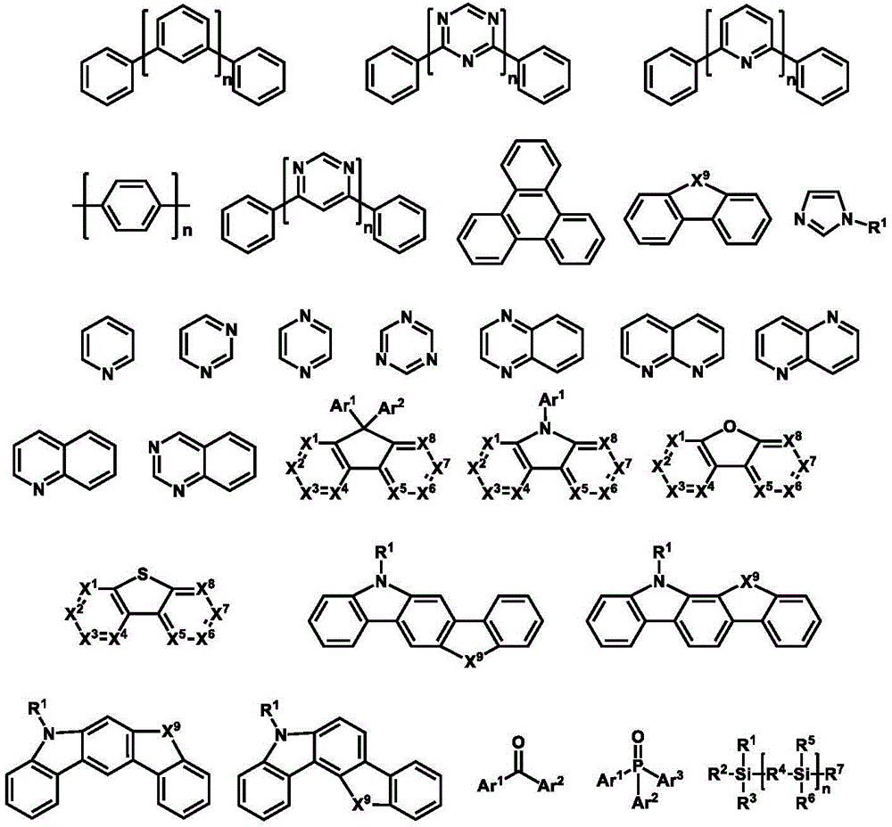
R1-R7可相互独立地选自如下的基团:氢,烷基,烷氧基,氨基,烯,炔,芳烷基,杂烷基,芳基和杂芳基,当它们是芳基或杂芳基时,它们与上述的Ar1和Ar2意义相同;n是一个从0到20的整数;X1-X8选自CH或N;X9选自CR1R2或NR1。R 1 -R 7 can be independently selected from the group consisting of hydrogen, alkyl, alkoxy, amino, alkene, alkyne, aralkyl, heteroalkyl, aryl and heteroaryl, when they are aryl In the case of radical or heteroaryl, they have the same meanings as the above-mentioned Ar 1 and Ar 2 ; n is an integer from 0 to 20; X 1 -X 8 are selected from CH or N; X 9 is selected from CR 1 R 2 or NR 1 .
在下面的表中列出合适的三重态主体材料的例子:Examples of suitable triplet host materials are listed in the table below:

3.单重态主体材料(Singlet Host):3. Singlet Host:
单重态主体材料的例子并不受特别的限制,任何有机化合物都可能被用作为主体,只要其单重态能量比发光体,特别是单重态发光体或荧光发光体更高。Examples of the singlet host material are not particularly limited, and any organic compound may be used as the host as long as its singlet energy is higher than that of an emitter, particularly a singlet emitter or a fluorescent emitter.
作为单重态主体材料使用的有机化合物的例子可选自含有环芳香烃化合物,如苯、联苯、三苯基、苯并、萘、蒽、萉、菲、芴、芘、屈、苝、薁;芳香杂环化合物,如二苯并噻吩、二苯并呋喃、二苯并硒吩、呋喃、噻吩、苯并呋喃、苯并噻吩、苯并硒吩、咔唑、吲哚咔唑、吡啶吲哚、吡咯二吡啶、吡唑、咪唑、三氮唑、异恶唑、噻唑、恶二唑、恶三唑、二恶唑、噻二唑、吡啶、哒嗪、嘧啶、吡嗪、三嗪、恶嗪、恶噻嗪、恶二嗪、吲哚、苯并咪唑、吲唑、吲哚嗪、苯并恶唑、苯异恶唑、苯并噻唑、喹啉、异喹啉、噌啉、喹唑啉、喹喔啉、萘、酞、蝶啶、氧杂蒽、吖啶、吩嗪、吩噻嗪、吩恶嗪、苯并呋喃吡啶、呋喃二吡啶、苯并噻吩吡啶、噻吩二吡啶、苯并硒吩吡啶和硒吩二吡啶;包含2至10环结构的基团,它们可以是相同或不同类型的环芳香烃基团或芳香杂环基团,并彼此直接或通过至少一个以下的基团连结在一起,如氧原子、氮原子、硫原子、硅原子、磷原子、硼原子、链结构单元和脂肪环基团。Examples of the organic compound used as the singlet host material can be selected from the group consisting of ring-containing aromatic hydrocarbon compounds such as benzene, biphenyl, triphenyl, benzo, naphthalene, anthracene, phenanthrene, phenanthrene, fluorene, pyrene, chrysene, perylene, Azulene; aromatic heterocyclic compounds such as dibenzothiophene, dibenzofuran, dibenzoselenophene, furan, thiophene, benzofuran, benzothiophene, benzoselenophene, carbazole, indolecarbazole, pyridine Indole, pyrrole dipyridine, pyrazole, imidazole, triazole, isoxazole, thiazole, oxadiazole, oxtriazole, dioxazole, thiadiazole, pyridine, pyridazine, pyrimidine, pyrazine, triazine , oxazine, oxthiazine, oxadiazine, indole, benzimidazole, indazole, indole, benzoxazole, benzisoxazole, benzothiazole, quinoline, isoquinoline, cinnoline, Quinazoline, quinoxaline, naphthalene, phthalein, pteridine, xanthene, acridine, phenazine, phenothiazine, phenoxazine, benzofuranpyridine, furandipyridine, benzothiophenepyridine, thiophenedipyridine , benzoselenophenepyridine and selenophenedipyridine; groups comprising 2 to 10 ring structures, which may be of the same or different types of cyclic aromatic hydrocarbon groups or aromatic heterocyclic groups, directly connected to each other or through at least one of the following Groups are linked together, such as oxygen atoms, nitrogen atoms, sulfur atoms, silicon atoms, phosphorus atoms, boron atoms, chain building blocks, and alicyclic groups.
在一个优选的实施方案中,单重态主体材料可选自包含至少一个以下基团的化合物:In a preferred embodiment, the singlet host material may be selected from compounds comprising at least one of the following groups:
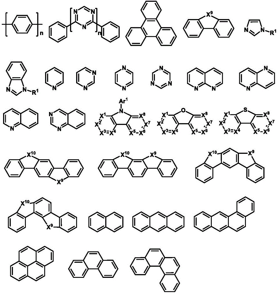
其中,R1可相互独立地选自如下的基团:氢、烷基、烷氧基、氨基、烯、炔、芳烷基、杂烷基、芳基和杂芳基;Ar1是芳基或杂芳基,它与上述的HTM中定义的Ar1意义相同;n是一个从0到20的整数;X1-X8选自CH或N;X9和X10选自CR1R2或NR1。wherein, R1 can be independently selected from the following groups: hydrogen, alkyl, alkoxy, amino, alkene, alkyne, aralkyl, heteroalkyl, aryl and heteroaryl ; Ar1 is aryl or Heteroaryl, which has the same meaning as Ar 1 defined in the above-mentioned HTM; n is an integer from 0 to 20; X 1 -X 8 are selected from CH or N; X 9 and X 10 are selected from CR 1 R 2 or NR 1 .
在下面的表中列出一些蒽基单重态主体材料的例子:Some examples of anthracene-based singlet host materials are listed in the table below:
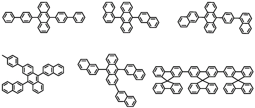
4.单重态发光体(Singlet Emitter)4. Singlet Emitter
单重态发光体往往有较长的共轭π电子系统。迄今,已有许多例子,例如在JP2913116B和WO2001021729A1中公开的苯乙烯胺及其衍生物,和在WO2008/006449和WO2007/140847中公开的茚并芴及其衍生物。Singlet emitters tend to have longer conjugated pi electron systems. To date, there have been many examples such as styrylamine and its derivatives disclosed in JP2913116B and WO2001021729A1, and indenofluorenes and its derivatives disclosed in WO2008/006449 and WO2007/140847.
在一个优选的实施方案中,单重态发光体可选自一元苯乙烯胺,二元苯乙烯胺,三元苯乙烯胺,四元苯乙烯胺,苯乙烯膦,苯乙烯醚和芳胺。In a preferred embodiment, the singlet emitter may be selected from the group consisting of monostyrylamines, di-styrylamines, tristyrylamines, tetrastyrylamines, styryl phosphines, styryl ethers and aromatic amines.
一个一元苯乙烯胺是指一化合物,它包含一个无取代或取代的苯乙烯基组和至少一个胺,最好是芳香胺。一个二元苯乙烯胺是指一化合物,它包含二个无取代或取代的苯乙烯基组和至少一个胺,最好是芳香胺。一个三元苯乙烯胺是指一化合物,它包含三个无取代或取代的苯乙烯基组和至少一个胺,最好是芳香胺。一个四元苯乙烯胺是指一化合物,它包含四个无取代或取代的苯乙烯基组和至少一个胺,最好是芳香胺。一个优选的苯乙烯是二苯乙烯,其可能会进一步被取代。相应的膦类和醚类的定义与胺类相似。芳基胺或芳香胺是指一种化合物,包含三个直接联接氮的无取代或取代的芳香环或杂环系统。这些芳香族或杂环的环系统中至少有一个优选选自稠环系统,并最好有至少14个芳香环原子。其中优选的例子有芳香蒽胺,芳香蒽二胺,芳香芘胺,芳香芘二胺,芳香屈胺和芳香屈二胺。一个芳香蒽胺是指一化合物,其中一个二元芳基胺基团直接联到蒽上,最好是在9的位置上。一个芳香蒽二胺是指一化合物,其中二个二元芳基胺基团直接联到蒽上,最好是在9,10的位置上。芳香芘胺,芳香芘二胺,芳香屈胺和芳香屈二胺的定义类似,其中二元芳基胺基团最好联到芘的1或1,6位置上.A monostyrylamine means a compound containing an unsubstituted or substituted styryl group and at least one amine, preferably an aromatic amine. A dibasic styrylamine refers to a compound containing two unsubstituted or substituted styryl groups and at least one amine, preferably an aromatic amine. A tristyrylamine refers to a compound containing three unsubstituted or substituted styryl groups and at least one amine, preferably an aromatic amine. A quaternary styrylamine refers to a compound containing four unsubstituted or substituted styryl groups and at least one amine, preferably an aromatic amine. A preferred styrene is stilbene, which may be further substituted. The corresponding phosphines and ethers are defined similarly to amines. Arylamine or aromatic amine refers to a compound containing three unsubstituted or substituted aromatic or heterocyclic ring systems directly attached to nitrogen. At least one of these aromatic or heterocyclic ring systems is preferably selected from fused ring systems and preferably has at least 14 aromatic ring atoms. Preferred examples of these are aromatic anthraceneamines, aromatic anthracene diamines, aromatic pyrene amines, aromatic pyrene diamines, aromatic drolidines and aromatic dridodiamines. An aromatic anthraceneamine refers to a compound in which a diarylamine group is attached directly to the anthracene, preferably in the 9 position. An aromatic anthracene diamine refers to a compound in which two diarylamine groups are attached directly to the anthracene, preferably in the 9,10 positions. Aromatic pyreneamines, aromatic pyrene diamines, aryl pyrene amines, and aryl pyrene diamines are similarly defined, with the divalent arylamine group preferably attached to the 1 or 1,6 position of the pyrene.
基于乙烯胺及芳胺的单重态发光体的例子,也是优选的例子,可在下述专利文件中找到:WO 2006/000388,WO 2006/058737,WO 2006/000389,WO 2007/065549,WO 2007/115610,US 7250532 B2,DE 102005058557 A1,CN 1583691 A,JP 08053397 A,US 6251531B1,US 2006/210830 A,EP 1957606 A1和US 2008/0113101 A1特此上述列出的专利文件中的全部内容并入本文作为参考。Examples of singlet emitters based on vinylamines and aromatic amines, which are also preferred, can be found in the following patent documents: WO 2006/000388, WO 2006/058737, WO 2006/000389, WO 2007/065549, WO 2007 /115610, US 7250532 B2, DE 102005058557 A1, CN 1583691 A, JP 08053397 A, US 6251531 B1, US 2006/210830 A, EP 1957606 A1 and US 2008/0113101 A1 are hereby incorporated in their entirety into the above-listed patent documents This article is for reference.
基于均二苯乙烯极其衍生物的单重态发光体的例子有US 5121029。Examples of singlet emitters based on stilbene and its derivatives are US 5121029.
进一步的优选的单重态发光体可选自茚并芴-胺和茚并芴-二胺,如WO 2006/122630所公开的,苯并茚并芴-胺和苯并茚并芴-二胺,如WO 2008/006449所公开的,二苯并茚并芴-胺和二苯并茚并芴-二胺,如WO2007/140847所公开的。Further preferred singlet emitters may be selected from indenofluorene-amines and indenofluorene-diamines, as disclosed in WO 2006/122630, benzoindenofluorene-amines and benzoindenofluorene-diamines , as disclosed in WO 2008/006449, dibenzoindenofluorene-amines and dibenzoindenofluorene-diamines, as disclosed in WO 2007/140847.
其他可用作单重态发光体的材料有多环芳烃化合物,特别是如下化合物的衍生物:蒽如9,10-二(2-萘并蒽),萘,四苯,氧杂蒽,菲,芘(如2,5,8,11-四-t-丁基苝),茚并芘,苯撑如(4,4’-双(9-乙基-3-咔唑乙烯基)-1,1’-联苯),二茚并芘,十环烯,六苯并苯,芴,螺二芴,芳基芘(如US20060222886),亚芳香基乙烯(如US5121029,US5130603),环戊二烯如四苯基环戊二烯,红荧烯,香豆素,若丹明,喹吖啶酮,吡喃如4(二氰基亚甲基)-6-(4-对二甲氨基苯乙烯基-2-甲基)-4H-吡喃(DCM),噻喃,双(吖嗪基)亚胺硼化合物(US 2007/0092753A1),双(吖嗪基)亚甲基化合物,carbostyryl化合物,噁嗪酮,苯并恶唑,苯并噻唑,苯并咪唑及吡咯并吡咯二酮。一些单重态发光体的材料可在下述专利文件中找到:US20070252517 A1,US 4769292,US 6020078,US 2007/0252517 A1,US 2007/0252517 A1。特此将上述列出的专利文件中的全部内容并入本文作为参考。Other materials that can be used as singlet emitters Polycyclic aromatic hydrocarbon compounds, especially derivatives of the following compounds: anthracene such as 9,10-bis(2-naphthanthracene), naphthalene, tetraphenyl, xanthene, phenanthrene , Pyrene (such as 2,5,8,11-tetra-t-butylperylene), indenopyrene, phenylene such as (4,4'-bis(9-ethyl-3-carbazole vinyl)-1 ,1'-biphenyl), bisindenopyrene, decacycloene, hexabenzone, fluorene, spirobifluorene, arylpyrene (such as US20060222886), arylene vinylene (such as US5121029, US5130603), cyclopentadiene Alkenes such as tetraphenylcyclopentadiene, rubrene, coumarin, rhodamine, quinacridone, pyrans such as 4(dicyanomethylene)-6-(4-p-dimethylaminobenzene Vinyl-2-methyl)-4H-pyran (DCM), thiopyran, bis(azinyl) imine boron compound (US 2007/0092753A1), bis(azinyl) methylene compound, carbostyryl compound , oxazinone, benzoxazole, benzothiazole, benzimidazole and diketopyrrolopyrrole. Materials for some singlet emitters can be found in the following patent documents: US20070252517 A1, US 4769292, US 6020078, US 2007/0252517 A1, US 2007/0252517 A1. The entire contents of the above-listed patent documents are hereby incorporated by reference.
在下面的表中列出一些合适的单重态发光体的例子:Some examples of suitable singlet emitters are listed in the table below:
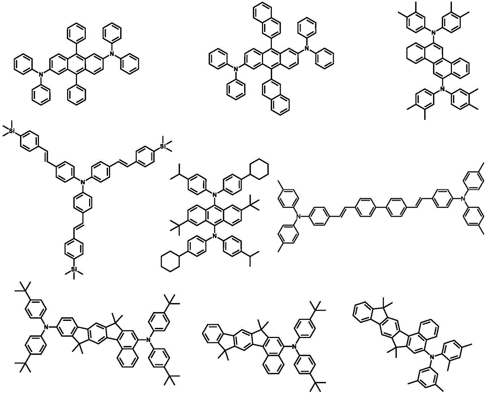
5.热激活延迟荧光发光材料(TADF):5. Thermally activated delayed fluorescence light-emitting material (TADF):
传统有机荧光材料只能利用电激发形成的25%单线态激子发光,器件的内量子效率较低(最高为25%)。尽管磷光材料由于重原子中心强的自旋-轨道耦合增强了系间穿越,可以有效利用电激发形成的单线态激子和三线态激子发光,使器件的内量子效率达到100%。但磷光材料昂贵,材料稳定性差,器件效率滚降严重等问题限制了其在OLED中的应用。热激活延迟荧光发光材料是继有机荧光材料和有机磷光材料之后发展的第三代有机发光材料。该类材料一般具有小的单线态-三线态能级差(ΔEst),三线态激子可以通过反系间穿越转变成单线态激子发光。这可以充分利用电激发下形成的单线态激子和三线态激子。器件内量子效率可达到100%。Traditional organic fluorescent materials can only use 25% of singlet excitons formed by electrical excitation to emit light, and the internal quantum efficiency of the device is low (up to 25%). Although the phosphorescent materials enhance intersystem crossing due to the strong spin-orbit coupling in the heavy atom center, the singlet and triplet excitons formed by electrical excitation can be effectively used to emit light, and the internal quantum efficiency of the device can reach 100%. However, the problems of expensive phosphorescent materials, poor material stability, and severe roll-off of device efficiency limit their application in OLEDs. Thermally activated delayed fluorescence light-emitting materials are the third generation of organic light-emitting materials developed after organic fluorescent materials and organic phosphorescent materials. Such materials generally have a small singlet-triplet energy level difference (ΔE st ), and triplet excitons can be transformed into singlet excitons through inverse intersystem crossing to emit light. This can take full advantage of the singlet and triplet excitons formed under electrical excitation. The internal quantum efficiency of the device can reach 100%.
TADF材料需要具有较小的单线态-三线态能级差,一般是ΔEst<0.3eV,较好是ΔEst<0.2eV,更好是ΔEst<0.1eV,最好是ΔEst<0.05eV。在一个优选的实施方案中,TADF有较好的荧光量子效率。一些TADF发光的材料可在下述专利文件中找到:CN103483332(A),TW201309696(A),TW201309778(A),TW201343874(A),TW201350558(A),US20120217869(A1),WO2013133359(A1),WO2013154064(A1),Adachi,et.al.Adv.Mater.,21,2009,4802,Adachi,et.al.Appl.Phys.Lett.,98,2011,083302,Adachi,et.al.Appl.Phys.Lett.,101,2012,093306,Adachi,et.al.Chem.Commun.,48,2012,11392,Adachi,et.al.NaturePhotonics,6,2012,253,Adachi,et.al.Nature,492,2012,234,Adachi,et.al.J.Am.Chem.Soc,134,2012,14706,Adachi,et.al.Angew.Chem.Int.Ed,51,2012,11311,Adachi,et.al.Chem.Commun.,48,2012,9580,Adachi,et.al.Chem.Commun.,48,2013,10385,Adachi,et.al.Adv.Mater.,25,2013,3319,Adachi,et.al.Adv.Mater.,25,2013,3707,Adachi,et.al.Chem.Mater.,25,2013,3038,Adachi,et.al.Chem.Mater.,25,2013,3766,Adachi,et.al.J.Mater.Chem.C.,1,2013,4599,Adachi,et.al.J.Phys.Chem.A.,117,2013,5607,特此将上述列出的专利或文章文件中的全部内容并入本文作为参考。The TADF material needs to have a small singlet-triplet energy level difference, generally ΔE st <0.3eV, preferably ΔE st <0.2eV, more preferably ΔE st <0.1eV, most preferably ΔE st <0.05eV. In a preferred embodiment, TADF has better fluorescence quantum efficiency. Some TADF luminescent materials can be found in the following patent documents: CN103483332(A), TW201309696(A), TW201309778(A), TW201343874(A), TW201350558(A), US20120217869(A1), WO2013133359(A1), WO2013154 A1), Adachi, et.al.Adv.Mater., 21, 2009, 4802, Adachi, et.al.Appl.Phys.Lett., 98, 2011, 083302, Adachi, et.al.Appl.Phys.Lett ., 101, 2012, 093306, Adachi, et. al. Chem. Commun., 48, 2012, 11392, Adachi, et. al. NaturePhotonics, 6, 2012, 253, Adachi, et. al. Nature, 492, 2012 , 234, Adachi, et.al.J.Am.Chem.Soc, 134, 2012, 14706, Adachi, et.al.Angew.Chem.Int.Ed, 51, 2012, 11311, Adachi, et.al.Chem .Commun., 48, 2012, 9580, Adachi, et.al.Chem.Commun., 48, 2013, 10385, Adachi, et.al.Adv.Mater., 25, 2013, 3319, Adachi, et.al. Adv.Mater., 25, 2013, 3707, Adachi, et.al.Chem.Mater., 25, 2013, 3038, Adachi, et.al.Chem.Mater., 25, 2013, 3766, Adachi, et.al .J.Mater.Chem.C.,1,2013,4599,Adachi,et.al.J.Phys.Chem.A.,117,2013,5607, all of the above-listed patent or article documents are hereby incorporated The contents are incorporated herein by reference.
在下面的表中列出一些合适的TADF发光材料的例子:Some examples of suitable TADF luminescent materials are listed in the table below:


6.三重态发光体(Triplet Emitter)6. Triplet Emitter
三重态发光体也称磷光发光体。在一个优选的实施方案中,三重态发光体是有通式M(L)n的金属络合物,其中M是一金属原子,L每次出现时可以是相同或不同,是一有机配体,它通过一个或多个位置键接或配位连接到金属原子M上,n是一个大于1的整数,较好选是1,2,3,4,5或6。可选地,这些金属络合物通过一个或多个位置联接到一个聚合物上,最好是通过有机配体。Triplet emitters are also called phosphorescent emitters. In a preferred embodiment, the triplet emitter is a metal complex having the general formula M(L) n , where M is a metal atom, L may be the same or different at each occurrence, and is an organic ligand , which is bonded or coordinated to the metal atom M through one or more positions, and n is an integer greater than 1, preferably 1, 2, 3, 4, 5 or 6. Optionally, the metal complexes are attached to a polymer through one or more sites, preferably through organic ligands.
在一个优选的实施方案中,金属原子M选自过渡金属元素或镧系元素或锕系元素,优选选择Ir,Pt,Pd,Au,Rh,Ru,Os,Sm,Eu,Gd,Tb,Dy,Re,Cu或Ag,特别优选选择Os,Ir,Ru,Rh,Re,Pd或Pt。In a preferred embodiment, the metal atom M is selected from transition metal elements or lanthanides or actinides, preferably Ir, Pt, Pd, Au, Rh, Ru, Os, Sm, Eu, Gd, Tb, Dy , Re, Cu or Ag, particularly preferably Os, Ir, Ru, Rh, Re, Pd or Pt.
优选地,三重态发光体包含螯合配体,即配体,通过至少两个结合点与金属配位,特别优选考虑的是三重态发光体包含两个或三个相同或不同的双齿或多齿配体。螯合配体有利于提高金属络合物的稳定性。Preferably, the triplet emitter comprises chelating ligands, i.e. ligands, which coordinate to the metal via at least two binding sites, it is particularly preferred that the triplet emitter comprises two or three identical or different bidentate or Polydentate ligands. Chelating ligands are beneficial to improve the stability of metal complexes.
有机配体的例子可选自苯基吡啶衍生物,7,8-苯并喹啉衍生物,2(2-噻吩基)吡啶衍生物,2(1-萘基)吡啶衍生物,或2苯基喹啉衍生物。所有这些有机配体都可能被取代,例如被含氟或三氟甲基取代。辅助配体可优选选自乙酸丙酮或苦味酸。Examples of organic ligands may be selected from phenylpyridine derivatives, 7,8-benzoquinoline derivatives, 2(2-thienyl)pyridine derivatives, 2(1-naphthyl)pyridine derivatives, or 2-benzene quinoline derivatives. All of these organic ligands may be substituted, eg by fluorine or trifluoromethyl. The auxiliary ligand may preferably be selected from acetone acetate or picric acid.
在一个优选的实施方案中,可用作三重态发光体的金属络合物有如下形式:In a preferred embodiment, metal complexes useful as triplet emitters are in the form:
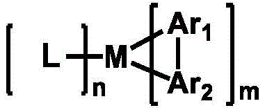
其中M是一金属,选自过渡金属元素或镧系元素或锕系元素;wherein M is a metal selected from transition metal elements or lanthanides or actinides;
Ar1每次出现时可以是相同或不同,是一个环状基团,其中至少包含一个施主原子,即有一孤对电子的原子,如氮或磷,通过它环状基团与金属配位连接;Ar2每次出现时可以是相同或不同,是一个环状基团,其中至少包含一个C原子,通过它环状基团与金属连接;Ar1和Ar2由共价键联接在一起,可各自携带一个或多个取代基团,它们也可再通过取代基团联接在一起;L每次出现时可以是相同或不同,是一个辅助配体,优选自双齿螯合配体,最好是单阴离子双齿螯合配体;m是1,2或3,优选地是2或3,特别优选地是3;n是0,1,或2,优选地是0或1,特别优选地是0;Ar 1 can be the same or different at each occurrence, is a cyclic group, which contains at least one donor atom, that is, an atom with a lone pair of electrons, such as nitrogen or phosphorus, through which the cyclic group is coordinated to the metal ; Ar 2 can be the same or different each time it appears, it is a cyclic group, which contains at least one C atom, through which the cyclic group is connected to the metal; Ar 1 and Ar 2 are linked together by covalent bonds, Each can carry one or more substituent groups, and they can also be linked together through the substituent groups; each occurrence of L can be the same or different, and is an auxiliary ligand, preferably from a bidentate chelating ligand, most Preferably a monoanionic bidentate chelating ligand; m is 1, 2 or 3, preferably 2 or 3, particularly preferably 3; n is 0, 1, or 2, preferably 0 or 1, particularly preferably ground is 0;
一些三重态发光体的材料极其应用的例子可在下述专利文件和文献中找到:WO200070655,WO 200141512,WO 200202714,WO 200215645,EP 1191613,EP 1191612,EP1191614,WO 2005033244,WO 2005019373,US 2005/0258742,WO 2009146770,WO2010015307,WO 2010031485,WO 2010054731,WO 2010054728,WO 2010086089,WO2010099852,WO 2010102709,US 20070087219 A1,US 20090061681 A1,US 20010053462A1,Baldo,Thompson et al.Nature 403,(2000),750-753,US 20090061681 A1,US20090061681 A1,Adachi et al.Appl.Phys.Lett.78(2001),1622-1624,J.Kido etal.Appl.Phys.Lett.65(1994),2124,Kido et al.Chem.Lett.657,1990,US 2007/0252517A1,Johnson et al.,JACS 105,1983,1795,Wrighton,JACS 96,1974,998,Ma et al.,Synth.Metals 94,1998,245,US 6824895,US 7029766,US 6835469,US 6830828,US20010053462 A1,WO 2007095118 A1,US 2012004407A1,WO 2012007088A1,WO2012007087A1,WO 2012007086A1,US 2008027220A1,WO 2011157339A1,CN 102282150A,WO 2009118087A1。特此将上述列出的专利文件和文献中的全部内容并入本文作为参考。Some examples of triplet emitter materials and their applications can be found in the following patent documents and documents: WO200070655, WO 200141512, WO 200202714, WO 200215645, EP 1191613, EP 1191612, EP1191614, WO 2005033244, WO 200501937423, US ,WO 2009146770,WO2010015307,WO 2010031485,WO 2010054731,WO 2010054728,WO 2010086089,WO2010099852,WO 2010102709,US 20070087219 A1,US 20090061681 A1,US 20010053462A1,Baldo,Thompson et al.Nature 403,(2000),750-753 , US 20090061681 A1, US20090061681 A1, Adachi et al.Appl.Phys.Lett.78 (2001), 1622-1624, J.Kido et al.Appl.Phys.Lett.65 (1994), 2124, Kido et al.Chem . Lett. 657, 1990, US 2007/0252517 A1, Johnson et al.,
在下面的表中列出一些合适的三重态发光体的例子:Some examples of suitable triplet emitters are listed in the table below:
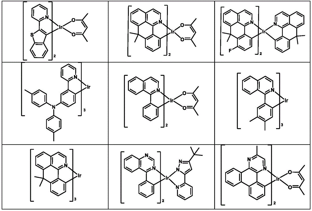
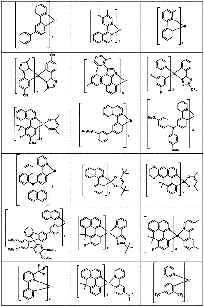

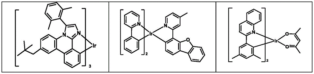
在另一个优选的实施方案中,按照本发明的印刷组合物包含的功能材料为高聚物材料。In another preferred embodiment, the functional material contained in the printing composition according to the present invention is a polymer material.
一般地,以上所述的有机小分子功能材料,包括HIM,HTM,ETM,EIM,Host,荧光发光体,磷光发光体,TADF都可以作为重复单元包含在一高聚物中。Generally, the above-mentioned organic small molecule functional materials, including HIM, HTM, ETM, EIM, Host, fluorescent emitters, phosphorescent emitters, and TADF can be contained in a high polymer as repeating units.
在一个优选的实施例中,适合于本发明的高聚物是共轭高聚物。一般地,共轭高聚物有如下通式:In a preferred embodiment, polymers suitable for the present invention are conjugated polymers. Generally, conjugated polymers have the following general formula:
其中B,A在多次出现时可独立选择相同或不同的结构单元Among them, B and A can independently select the same or different structural units when they appear multiple times
B:具有较大的能隙的π-共轭结构单元,也称骨干单元(Backbone Unit),选自单环或多环芳基或杂芳基,优选选择的单元形式为苯,联二亚苯(Biphenylene),萘,蒽,菲,二氢菲,9,10-二氢菲,芴,二芴,螺二芴,对苯乙炔,反茚并芴,顺茚并,二苯并-茚并芴,茚并萘及它们的衍生物.B: a π-conjugated structural unit with a larger energy gap, also known as a backbone unit (Backbone Unit), selected from monocyclic or polycyclic aryl or heteroaryl, and preferably the selected unit form is benzene, bidiline Benzene (Biphenylene), naphthalene, anthracene, phenanthrene, dihydrophenanthrene, 9,10-dihydrophenanthrene, fluorene, difluorene, spirobifluorene, p-phenylacetylene, trans-indenofluorene, cis-indeno, dibenzo-indene Fluorene, indenaphthalene and their derivatives.
A:具有较小能隙的π-共轭结构单元,也称功能单元(Functional Unit),按照不同的功能要求,可选自包含以上所述的空穴注入或传输材料(HIM/HTM),电子注入或传输材料(EIM/ETM),主体材料(Host),单重态发光体(荧光发光体),重态发光体(磷光发光体)的结构单元。A: A π-conjugated structural unit with a smaller energy gap, also known as a functional unit, can be selected from the hole injection or transport materials (HIM/HTM) described above according to different functional requirements, Structural unit of electron injection or transport material (EIM/ETM), host material (Host), singlet emitter (fluorescence emitter), doublet emitter (phosphorescence emitter).
x,y:>0,且x+y=1;x,y:>0, and x+y=1;
在某些较为优选的实施例中,按照本发明的印刷组合物包含的功能材料为高聚物HTM。In some more preferred embodiments, the functional material contained in the printing composition according to the present invention is high polymer HTM.
在一个优选的实施例中,高聚物HTM材料为均聚物,优选的均聚物选自聚噻吩,聚吡咯,聚苯胺,聚联苯类三芳胺,聚乙烯基咔唑及它们的衍生物.In a preferred embodiment, the high polymer HTM material is a homopolymer, and the preferred homopolymer is selected from polythiophene, polypyrrole, polyaniline, polybiphenyl triarylamine, polyvinyl carbazole and their derivatives thing.
在另一个特别优选的实施例中,高聚物HTM材料为化学式1表示的共轭共聚物,其中In another particularly preferred embodiment, the high polymer HTM material is a conjugated copolymer represented by Chemical Formula 1, wherein
A:具有空穴输运能力的功能基团,可相同或不同地选自包含以上所述的空穴注入或传输材料(HIM/HTM)的结构单元;在一个优选的实施例中,A选自胺,联苯类三芳胺,噻吩,并噻吩如二噻吩并噻吩和并噻吩,吡咯,苯胺,咔唑,indenocarbazole,氮茚并氮芴,并五苯,酞菁,卟啉及它们的衍生物.A: a functional group with hole transport capability, which can be selected from the same or different structural units comprising the hole injection or transport material (HIM/HTM) described above; in a preferred embodiment, A is selected from From amines, biphenyl triarylamines, thiophenes, thiophenes such as dithienothiophenes and thiophenes, pyrroles, anilines, carbazoles, indenocarbazole, indenoazepines, pentacene, phthalocyanines, porphyrins and their derivatives thing.
x,y:>0,且x+y=1;通常y≥0.10,比较好为≥0.15,更好为≥0.20,最好为x=y=0.5.x, y:>0, and x+y=1; usually y≥0.10, preferably ≥0.15, more preferably ≥0.20, preferably x=y=0.5.
在下面列出合适的可作为HTM的共轭高聚物的例子:Examples of suitable HTM conjugated polymers are listed below:
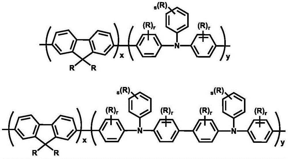
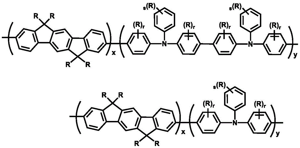
其中,in,
R各自彼此独立地是氢,具有1至20个C原子的直链烷基、烷氧基或硫代烷氧基基团,或者具有3至20个C原子的支链或环状的烷基、烷氧基或硫代烷氧基基团或者是甲硅烷基基团,或具有1至20个C原子的取代的酮基基团,或具有2至20个C原子的烷氧基羰基基团,或具有7至20个C原子的芳氧基羰基基团,氰基基团(-CN),氨基甲酰基基团(-C(=O)NH2),卤甲酰基基团(-C(=O)-X其中X代表卤素原子),甲酰基基团(-C(=O)-H),异氰基基团,异氰酸酯基团,硫氰酸酯基团或异硫氰酸酯基团,羟基基团,硝基基团,CF3基团,Cl,Br,F,可交联的基团或者具有5至40个环原子的取代或未取代的芳族或杂芳族环系,或具有5至40个环原子的芳氧基或杂芳氧基基团,或这些体系的组合,其中一个或多个基团R可以彼此和/或与所述基团R键合的环形成单环或多环的脂族或芳族环系;R is each independently of one another hydrogen, a straight-chain alkyl, alkoxy or thioalkoxy group having 1 to 20 C atoms, or a branched or cyclic alkyl group having 3 to 20 C atoms , an alkoxy or thioalkoxy group or a silyl group, or a substituted keto group having 1 to 20 C atoms, or an alkoxycarbonyl group having 2 to 20 C atoms group, or an aryloxycarbonyl group having 7 to 20 C atoms, a cyano group (-CN), a carbamoyl group (-C(=O) NH2 ), a haloformyl group (- C(=O)-X where X represents a halogen atom), formyl group (-C(=O)-H), isocyano group, isocyanate group, thiocyanate group or isothiocyanate Ester groups, hydroxyl groups, nitro groups, CF3 groups, Cl, Br, F, crosslinkable groups or substituted or unsubstituted aromatic or heteroaromatic rings with 5 to 40 ring atoms systems, or aryloxy or heteroaryloxy groups having 5 to 40 ring atoms, or a combination of these systems, wherein one or more groups R may be bonded to each other and/or to said groups R The rings form a monocyclic or polycyclic aliphatic or aromatic ring system;
r 是0,1,2,3或4;r is 0, 1, 2, 3 or 4;
s 是0,1,2,3,4或5;s is 0, 1, 2, 3, 4 or 5;
x,y: >0,且x+y=1;通常y≥0.10,比较好为≥0.15,更好为≥0.20,最好为x=y=0.5。x, y: >0, and x+y=1; usually y≥0.10, preferably ≥0.15, more preferably ≥0.20, and most preferably x=y=0.5.
另一类优选选择的有机功能材料是具有电子传输能力的高聚物,包括共轭高聚物和非共轭高聚物。Another type of organic functional materials that are preferably selected are polymers with electron transport ability, including conjugated polymers and non-conjugated polymers.
优选选择的高聚物ETM材料为均聚物,优选的均聚物选自聚菲,聚菲罗啉,聚茚并芴,聚螺二芴,聚芴及它们的衍生物。The preferred high polymer ETM material is a homopolymer, and the preferred homopolymer is selected from polyphenanthrene, polyphenanthroline, polyindenofluorene, polyspirobifluorene, polyfluorene and their derivatives.
优选选择的高聚物ETM材料为化学式1表示的共轭共聚物,其中A在多次出现时可独立选择相同或不同的形式:The preferably selected high polymer ETM material is a conjugated copolymer represented by chemical formula 1, wherein A can be independently selected in the same or different form when it appears multiple times:
A:具有电子输运能力的功能基,优选选自三(8-羟基喹啉)铝(AlQ3),苯,联二亚苯,萘,蒽,菲,Dihydrophenanthrene,芴,二芴,螺二芴,对苯乙炔,芘,苝,9,10-Dihydrophenanthrene,吩嗪,菲罗啉,反茚并芴,顺茚并,二苯并-茚并芴,茚并萘,苯并蒽及它们的衍生物A: functional group with electron transport ability, preferably selected from tris(8-hydroxyquinoline)aluminum (AlQ3), benzene, biphenylene, naphthalene, anthracene, phenanthrene, Dihydrophenanthrene, fluorene, difluorene, spirobifluorene , p-phenylacetylene, pyrene, perylene, 9,10-Dihydrophenanthrene, phenazine, phenanthrene, trans-indenofluorene, cis-indeno, dibenzo-indenofluorene, indenaphthalene, benzanthracene and their derivatives thing
x,y:>0,且x+y=1.通常y≥0.10,比较好为≥0.15,更好为≥0.20,最好为x=y=0.5.x,y:>0, and x+y=1. Usually y≥0.10, preferably ≥0.15, more preferably ≥0.20, preferably x=y=0.5.
在另一个优选的实施方案中,按照本发明的印刷组合物包含的功能材料为发光高聚物。In another preferred embodiment, the functional material contained in the printing composition according to the present invention is a light-emitting polymer.
在一个特别优选的实施例中,发光高聚物是有如下通式的共轭高聚物高聚物有如下通式:In a particularly preferred embodiment, the light-emitting polymer is a conjugated polymer having the following general formula The high polymer has the following general formula:
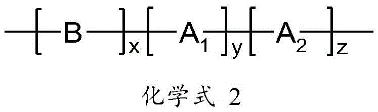
B:与化学式1的定义相同。B: The same as the definition of Chemical Formula 1.
A1:具有空穴或电子输运能力的功能基,可选自包含以上所述的空穴注入或传输材料(HIM/HTM),或电子注入或传输材料(EIM/ETM)的结构单元。A1: A functional group with hole or electron transport capability, which can be selected from structural units comprising the above-mentioned hole injection or transport material (HIM/HTM), or electron injection or transport material (EIM/ETM).
A2:具有发光功能的基团,可选自包含以上所述的单重态发光体(荧光发光体),重态发光体(磷光发光体)的结构单元。A2: A group with a light-emitting function, which can be selected from the structural units comprising the singlet emitter (fluorescence emitter) and the doublet emitter (phosphorescence emitter) described above.
x,y,z:>0,且x+y+z=1;x,y,z:>0, and x+y+z=1;
发光高聚物的例子在如下的专利申请中公开:WO2007043495,WO2006118345,WO2006114364,WO2006062226,WO2006052457,WO2005104264,WO2005056633,WO2005033174,WO2004113412,WO2004041901,WO2003099901,WO2003051092,WO2003020790,WO2003020790,US2020040076853,US2020040002576,US2007208567,US2005962631,EP201345477,EP2001344788,DE102004020298,特将以上专利文件中的全部内容并入本文作为参考。发光高聚物的例子在如下的专利申请中公开:WO2007043495,WO2006118345,WO2006114364,WO2006062226,WO2006052457,WO2005104264,WO2005056633,WO2005033174,WO2004113412,WO2004041901,WO2003099901,WO2003051092,WO2003020790,WO2003020790,US2020040076853,US2020040002576,US2007208567,US2005962631, EP201345477, EP2001344788, DE102004020298, the entire contents of the above patent documents are hereby incorporated by reference.
在另一个的实施例中,适合于本发明的高聚物是非共轭高聚物。这可以是所有功能基团都在侧链上,而主链是非共轭的高聚物。一些用作磷光主体或磷光发光材料的这类非共轭高聚物在US 7250226 B2,JP2007059939A,JP2007211243A2和JP2007197574A2等专利申请中有公开,一些用作荧光发光材料的这类非共轭高聚物在JP2005108556,JP2005285661和JP2003338375等专利申请中有公开。另外,非共轭高聚物也可以是一种高聚物,主链上共轭的功能单元通过非共轭的链接单元链接起来,这种高聚物的例子在DE102009023154.4和DE102009023156.0中有公开。特将以上专利文件中的全部内容并入本文作为参考。In another embodiment, polymers suitable for the present invention are non-conjugated polymers. This can be where all functional groups are on the side chains and the main chain is a non-conjugated polymer. Some such non-conjugated polymers used as phosphorescent host or phosphorescent light-emitting material are disclosed in patent applications such as US 7250226 B2, JP2007059939A, JP2007211243A2 and JP2007197574A2, and some such non-conjugated polymers used as fluorescent light-emitting materials It is disclosed in patent applications such as JP2005108556, JP2005285661 and JP2003338375. In addition, the non-conjugated polymer can also be a polymer, and the conjugated functional units on the main chain are linked by non-conjugated linking units. Examples of such polymers are in DE102009023154.4 and DE102009023156.0 There are public. The entire contents of the above patent documents are hereby incorporated by reference.
本发明还涉及一种通过印刷或涂布的方法制备包含功能材料的薄膜的方法,其中将如上所述的任何一种印刷组合物用印刷或涂布的方法涂布于一基板上,其中印刷或涂布的方法可选自(但不限于)喷墨打印,喷印(Nozzle Printing),活版印刷,丝网印刷,浸涂,旋转涂布,刮刀涂布,辊筒印花,扭转辊印刷,平版印刷,柔版印刷,轮转印刷,喷涂,刷涂或移印,狭缝型挤压式涂布等。The present invention also relates to a method for preparing a film comprising a functional material by a method of printing or coating, wherein any one of the printing compositions as described above is applied to a substrate by a method of printing or coating, wherein the printing Or the method of coating can be selected from (but not limited to) ink jet printing, jet printing (Nozzle Printing), letterpress printing, screen printing, dip coating, spin coating, blade coating, roll printing, reverse roll printing, Lithographic printing, flexographic printing, rotary printing, spray coating, brush coating or pad printing, slot extrusion coating, etc.
在一个优选的实施例中,包含功能材料的薄膜为通过喷墨打印的方法制备。可用于打印按照本发明的油墨的喷墨打印机为已商业化的打印机,且包含按需打印喷头(drop-on-demand printheads)。这些打印机可以从Fujifilm Dimatix(Lebanon,N.H.),TridentInternational(Brookfield,Conn.),Epson(Torrance,Calif),Hitachi Data systemsCorporation(Santa Clara,Calif),Xaar PLC(Cambridge,United Kingdom),和IdanitTechnologies,Limited(Rishon Le Zion,Isreal)购得。例如,本发明可以使用DimatixMaterials Printer DMP-3000(Fujifilm)进行打印。In a preferred embodiment, the thin film containing the functional material is prepared by an inkjet printing method. Inkjet printers that can be used to print inks according to the present invention are commercial printers and include drop-on-demand printheads. These printers are available from Fujifilm Dimatix (Lebanon, N.H.), Trident International (Brookfield, Conn.), Epson (Torrance, Calif), Hitachi Data systems Corporation (Santa Clara, Calif), Xaar PLC (Cambridge, United Kingdom), and Idanit Technologies, Limited (Rishon Le Zion, Isreal). For example, the present invention can be printed using a DimatixMaterials Printer DMP-3000 (Fujifilm).
本发明进一步涉及一电子器件,包含一层或多层功能薄膜,其中至少有一层功能薄膜是利用按照本发明的印刷组合物制备,特别是通过印刷或涂布的方法制备。The invention further relates to an electronic device comprising one or more functional films, wherein at least one functional film is produced using the printing composition according to the invention, in particular by printing or coating.
合适的电子器件包括但不限于量子点发光二极管(QLED)、量子点光伏电池(QPV)、量子点发光电池(QLEEC)、量子点场效应管(QFET)、量子点发光场效应管、量子点激光器,量子点传感器,有机发光二极管(OLED)、有机光伏电池(OPV)、有机发光电池(OLEEC)、有机场效应管(OFET)、有机发光场效应管、有机激光器,有机传感器等。Suitable electronic devices include, but are not limited to, quantum dot light emitting diodes (QLED), quantum dot photovoltaic cells (QPV), quantum dot light emitting cells (QLEEC), quantum dot field effect transistors (QFET), quantum dot light emitting field effect transistors, quantum dots Lasers, quantum dot sensors, organic light emitting diodes (OLED), organic photovoltaic cells (OPV), organic light emitting cells (OLEEC), organic field effect transistors (OFET), organic light emitting field effect transistors, organic lasers, organic sensors, etc.
在一个优选的实施例中,以上所述的电子器件是电致发光器件或光伏电池,如图一所示,包括一基片(101),一阳极(102),至少一发光层或光吸收层(104),一阴极(106)。以下仅针对电致发光器件做说明。In a preferred embodiment, the above-mentioned electronic device is an electroluminescent device or a photovoltaic cell, as shown in Figure 1, comprising a substrate (101), an anode (102), at least one light-emitting layer or light-absorbing layer layer (104), a cathode (106). Only the electroluminescent device will be described below.
基片(101)可以是不透明或透明的。一个透明的基板可以用来制造一个透明的发光元器件。例如可参见,Bulovic等Nature 1996,380,p29,和Gu等,Appl.Phys.Lett.1996,68,p2606。基材可以是刚性的或弹性的。基片可以是塑料,金属,半导体晶片或玻璃。最好是基片有一个平滑的表面。无表面缺陷的基板是特别理想的选择。在一个优选的实施例中,基片可选自聚合物薄膜或塑料,其玻璃化温度Tg为150℃以上,较好是超过200℃,更好是超过250℃,最好是超过300℃。合适的基板的例子有聚(对苯二甲酸乙二醇酯)(PET)和聚乙二醇(2,6-萘)(PEN)。The substrate (101) may be opaque or transparent. A transparent substrate can be used to fabricate a transparent light-emitting device. See, eg, Bulovic et al. Nature 1996, 380, p29, and Gu et al., Appl. Phys. Lett. 1996, 68, p2606. The substrate can be rigid or elastic. The substrate can be plastic, metal, semiconductor wafer or glass. Preferably the substrate has a smooth surface. Substrates free of surface defects are particularly desirable. In a preferred embodiment, the substrate can be selected from polymer films or plastics with a glass transition temperature Tg above 150°C, preferably above 200°C, more preferably above 250°C, most preferably above 300°C. Examples of suitable substrates are poly(ethylene terephthalate) (PET) and polyethylene glycol (2,6-naphthalene) (PEN).
阳极(102)可包括一导电金属或金属氧化物,或导电聚合物。阳极可以容易地注入空穴到HIL或HTL或发光层中。在一个的实施例中,阳极的功函数和作为HIL或HTL的p型半导体材料的HOMO能级或价带能级的差的绝对值小于0.5eV,较好是小于0.3eV,最好是小于0.2eV。阳极材料的例子包括但不限于,Al,Cu,Au,Ag,Mg,Fe,Co,Ni,Mn,Pd,Pt,ITO,铝掺杂氧化锌(AZO)等。其他合适的阳极材料是已知的,本领域普通技术人员可容易地选择使用。阳极材料可以使用任何合适的技术沉积,如一合适的物理气相沉积法,包括射频磁控溅射,真空热蒸发,电子束(e-beam)等。The anode (102) may comprise a conductive metal or metal oxide, or a conductive polymer. The anode can easily inject holes into the HIL or HTL or light emitting layer. In one embodiment, the absolute value of the difference between the work function of the anode and the HOMO energy level or valence band energy level of the p-type semiconductor material as the HIL or HTL is less than 0.5eV, preferably less than 0.3eV, most preferably less than 0.2eV. Examples of anode materials include, but are not limited to, Al, Cu, Au, Ag, Mg, Fe, Co, Ni, Mn, Pd, Pt, ITO, aluminum doped zinc oxide (AZO), and the like. Other suitable anode materials are known and can be readily selected for use by those of ordinary skill in the art. The anode material may be deposited using any suitable technique, such as a suitable physical vapor deposition method, including radio frequency magnetron sputtering, vacuum thermal evaporation, electron beam (e-beam), and the like.
在某些实施例中,阳极是图案结构化的。图案化的ITO导电基板可在市场上买到,并且可以用来制备根据本发明的器件。In certain embodiments, the anode is pattern-structured. Patterned ITO conductive substrates are commercially available and can be used to fabricate devices according to the present invention.
阴极(106)可包括一导电金属或金属氧化物。阴极可以容易地注入电子到EIL或ETL或直接到发光层中。在一个的实施例中,阴极的功函数和作为EIL或ETL或HBL的n型半导体材料的LUMO能级或导带能级的差的绝对值小于0.5eV,较好是小于0.3eV,最好是小于0.2eV。原则上,所有可用作OLED的阴极的材料都可能作为本发明器件的阴极材料。阴极材料的例子包括但不限于,Al,Au,Ag,Ca,Ba,Mg,LiF/Al,MgAg合金,BaF2/Al,Cu,Fe,Co,Ni,Mn,Pd,Pt,ITO等。阴极材料可以使用任何合适的技术沉积,如一合适的物理气相沉积法,包括射频磁控溅射,真空热蒸发,电子束(e-beam)等。The cathode (106) may comprise a conductive metal or metal oxide. The cathode can easily inject electrons into the EIL or ETL or directly into the emissive layer. In one embodiment, the absolute value of the difference between the work function of the cathode and the LUMO level or conduction band level of the n-type semiconductor material as EIL or ETL or HBL is less than 0.5 eV, preferably less than 0.3 eV, most preferably less than 0.5 eV. is less than 0.2eV. In principle, all materials that can be used as cathodes for OLEDs are possible as cathode materials for the devices of the invention. Examples of cathode materials include, but are not limited to, Al, Au, Ag, Ca, Ba, Mg, LiF/Al, MgAg alloys, BaF2/Al, Cu, Fe, Co, Ni, Mn, Pd, Pt, ITO, and the like. The cathode material can be deposited using any suitable technique, such as a suitable physical vapor deposition method, including radio frequency magnetron sputtering, vacuum thermal evaporation, electron beam (e-beam), and the like.
发光层(104)中至少包含一发光功能材料,其厚度可以在2nm到200nm之间。在一个优选的实施例中,按照本发明的发光器件中,其发光层是通过打印本发明的印刷油墨制备而成,其中印刷油墨中包含至少一种如上所述的发光功能材料,特别是量子点或有机功能材料。The light-emitting layer (104) contains at least one light-emitting functional material, and its thickness can be between 2 nm and 200 nm. In a preferred embodiment, in the light-emitting device according to the present invention, the light-emitting layer thereof is prepared by printing the printing ink of the present invention, wherein the printing ink contains at least one of the above-mentioned light-emitting functional materials, especially quantum dots or organic functional materials.
在一个优选的实施例中,按照本发明的发光器件进一步包含一个空穴注层(HIL)或空穴传输层(HTL)(103),其中包含如上所述的有机HTM或无机p型材料。在一个优选的实施例中,HIL或HTL可以通过打印本发明的印刷油墨制备而成,其中印刷油墨中包含具有空穴传输能力的功能材料,特别是量子点或有机HTM材料。In a preferred embodiment, the light emitting device according to the present invention further comprises a hole injection layer (HIL) or hole transport layer (HTL) (103) comprising an organic HTM or inorganic p-type material as described above. In a preferred embodiment, HIL or HTL can be prepared by printing the printing ink of the present invention, wherein the printing ink contains functional materials with hole transport capability, especially quantum dots or organic HTM materials.
在另一个优选的实施例中,按照本发明的发光器件进一步包含一个电子注层(EIL)或电子传输层(ETL)(105),其中包含如上所述的有机ETM或无机n型材料。在某些实施例中,EIL或ETL可以通过打印本发明的印刷油墨制备而成,其中印刷油墨中包含具有电子传输能力的功能材料,特别是量子点或有机ETM材料。In another preferred embodiment, the light emitting device according to the present invention further comprises an electron injection layer (EIL) or electron transport layer (ETL) (105) comprising an organic ETM or inorganic n-type material as described above. In certain embodiments, EILs or ETLs can be prepared by printing the printing inks of the present invention, wherein the printing inks contain functional materials with electron transport capabilities, particularly quantum dots or organic ETM materials.
本发明还涉及按照本发明的发光器件在各种场合的应用,包括,但不限于,各种显示器件,背光源,照明光源等。The present invention also relates to the application of the light-emitting device according to the present invention in various occasions, including, but not limited to, various display devices, backlight sources, illumination sources, and the like.
下面将结合优选实施例对本发明进行了说明,但本发明并不局限于下述实施例,应当理解,所附权利要求概括了本发明的范围在本发明构思的引导下本领域的技术人员应意识到,对本发明的各实施例所进行的一定的改变,都将被本发明的权利要求书的精神和范围所覆盖。The present invention will be described below in conjunction with the preferred embodiments, but the present invention is not limited to the following embodiments. It should be understood that the appended claims summarize the scope of the present invention. Under the guidance of the inventive concept, those skilled in the art should It is appreciated that certain changes made to the various embodiments of the present invention will be covered by the spirit and scope of the claims of the present invention.
实施例:Example:
实施例1:蓝光量子点的制备(CdZnS/ZnS)Example 1: Preparation of blue light quantum dots (CdZnS/ZnS)
称取0.0512g的S和量取2.4mLODE于25mL的单口烧瓶中,置于油锅中加热至80℃使S溶解,备用,以下简称溶液1;称取0.1280g的S和量取5mLOA于25mL的单口烧瓶中,置于油锅中加热至90℃使S溶解,备用,以下简称溶液2;称量0.1028gCdO和1.4680g的乙酸锌,量取5.6mL的OA于50mL的三口烧瓶中,将三口烧瓶置于150mL的加热套中,两边瓶口用胶塞塞住,上方连接一个冷凝管,再连接至双排管,加热至150℃,抽真空40min,再通氮气;用注射器将12mL的ODE加入到三口烧瓶中,升温至310℃时快速用注射器将1.92mL的溶液1打进三口烧瓶中,计时12min;12min一到,用注射器将4mL的溶液2滴加至三口烧瓶中,滴加速度大约为0.5mL/min,反应3h,停止反应,立刻把三口烧瓶放入水中冷却至150℃;Weigh 0.0512g of S and measure 2.4mL of LODE in a 25mL single-necked flask, place in an oil pan and heat to 80°C to dissolve S, for later use, hereinafter referred to as solution 1; weigh 0.1280g of S and measure 5mL of OA in 25mL In the single-necked flask of 0.1028g CdO and 1.4680g of zinc acetate, measure 5.6mL of OA in a 50mL three-necked flask, and put it in a 50mL three-necked flask. The three-necked flask was placed in a 150 mL heating mantle, the two sides of the flask were plugged with rubber stoppers, a condenser tube was connected above, and then connected to a double-row tube, heated to 150 ° C, vacuumed for 40 min, and then filled with nitrogen; the 12 mL of ODE was added to the three-necked flask, and when the temperature was raised to 310 °C, 1.92 mL of solution 1 was quickly injected into the three-necked flask with a syringe, and the timing was 12 minutes; when 12 minutes arrived, 4 mL of solution 2 was added dropwise to the three-necked flask with a syringe, and the rate of addition was increased. About 0.5mL/min, react for 3h, stop the reaction, immediately put the three-necked flask into water and cool it to 150℃;
将过量的正己烷加入至三口烧瓶中,然后将三口烧瓶中的液体转移至多个10mL的离心管中,离心,除去下层沉淀,重复三次;在经过后处理1的液体中加入丙酮至有沉淀产生,离心,除去上层清液,留下沉淀;再用正己烷溶解沉淀,后加丙酮至有沉淀出来,离心,除去上层清液,留下沉淀,重复三次;最后用甲苯溶解沉淀,转移至玻璃瓶中存储。Add excess n-hexane to the three-necked flask, then transfer the liquid in the three-necked flask to a plurality of 10mL centrifuge tubes, centrifuge, remove the lower layer precipitate, repeat three times; add acetone to the liquid after post-treatment 1 until there is a precipitate. , centrifuge, remove the supernatant, leave the precipitate; dissolve the precipitate with n-hexane, then add acetone until there is a precipitate, centrifuge, remove the supernatant, leave the precipitate, repeat three times; finally dissolve the precipitate with toluene, transfer to glass Store in bottle.
实施例2:绿光量子点的制备(CdZnSeS/ZnS)Example 2: Preparation of green quantum dots (CdZnSeS/ZnS)
称量0.0079g的硒和0.1122g的硫于25mL的单口烧瓶中,量取2mL的TOP,通氮气,搅拌,备用,以下简称溶液1;称量0.0128g的CdO和0.3670g的乙酸锌,量取2.5mL的OA于25mL的三口烧瓶中,两边瓶口用胶塞塞住,上方连接一个冷凝管,再连接至双排管,将三口烧瓶置于50mL的加热套中,抽真空通氮气,加热至150℃,抽真空30min,注射7.5mL的ODE,再加热至300℃快速注射1mL的溶液1,计时10min;10min一到,立刻停止反应,将三口烧瓶置于水中冷却。Weigh 0.0079g of selenium and 0.1122g of sulfur into a 25mL single-necked flask, measure 2mL of TOP, pass nitrogen, stir, and set aside, hereinafter referred to as solution 1; weigh 0.0128g of CdO and 0.3670g of zinc acetate, the amount Take 2.5mL of OA into a 25mL three-necked flask, plug the bottle necks on both sides with rubber stoppers, connect a condenser tube above, and then connect it to a double-row tube, place the three-necked flask in a 50mL heating mantle, evacuate and pass nitrogen, Heated to 150°C, evacuated for 30min, injected 7.5mL of ODE, then heated to 300°C and quickly injected 1mL of solution 1, timing for 10min; when 10min was up, the reaction was stopped immediately, and the three-necked flask was placed in water to cool.
往三口烧瓶中加入5mL的正己烷,然后就混合液加入至多个10mL的离心管中,加入丙酮至有沉淀出来,离心。取沉淀,除去上层清液,用正己烷将沉淀溶解,加入丙酮至有沉淀产生,离心。重复三次。最后的沉淀用少量的甲苯溶解,转移至玻璃瓶中储存。Add 5 mL of n-hexane to the three-necked flask, then add the mixture to a plurality of 10 mL centrifuge tubes, add acetone to precipitate out, and centrifuge. Take the precipitate, remove the supernatant, dissolve the precipitate with n-hexane, add acetone until a precipitate is formed, and centrifuge. repeat three times. The final pellet was dissolved with a small amount of toluene and transferred to a glass bottle for storage.
实施例3:红光量子点的制备(CdSe/CdS/ZnS)Example 3: Preparation of red quantum dots (CdSe/CdS/ZnS)
1mmol的CdO,4mmol的OA和20ml的ODE加入到100ml三口烧瓶中,鼓氮气,升温至300℃形成Cd(OA)2前驱体.在此温度下,快速注入0.25mL的溶有0.25mmol的Se粉的TOP。反应液在此温度下反应90秒,生长得到约3.5纳米的CdSe核。0.75mmol的辛硫醇在300℃下逐滴加入到反应液中,反应30分钟后生长约1纳米厚的CdS壳。4mmol的Zn(OA)2和2ml的溶有4mmol的S粉的TBP随后逐滴加入到反应液中,用以生长ZnS壳(约1纳米)。反应持续10分钟后,冷却至室温。1mmol of CdO, 4mmol of OA and 20ml of ODE were added to a 100ml three-necked flask, nitrogen was bubbled, and the temperature was raised to 300°C to form a Cd(OA) 2 precursor. At this temperature, 0.25mL of Se dissolved in 0.25mmol was rapidly injected TOP of powder. The reaction solution was reacted at this temperature for 90 seconds, and a CdSe core of about 3.5 nanometers was grown. 0.75 mmol of octanethiol was added dropwise to the reaction solution at 300 °C, and a CdS shell with a thickness of about 1 nm was grown after 30 minutes of reaction. 4 mmol of Zn(OA) 2 and 2 ml of TBP dissolved in 4 mmol of S powder were then added dropwise to the reaction solution to grow ZnS shells (about 1 nm). After the reaction continued for 10 minutes, it was cooled to room temperature.
往三口烧瓶中加入5mL的正己烷,然后就混合液加入至多个10mL的离心管中,加入丙酮至有沉淀出来,离心。取沉淀,除去上层清液,用正己烷将沉淀溶解,加入丙酮至有沉淀产生,离心。重复三次。最后的沉淀用少量的甲苯溶解,转移至玻璃瓶中储存。Add 5 mL of n-hexane to the three-necked flask, then add the mixture to a plurality of 10 mL centrifuge tubes, add acetone to precipitate out, and centrifuge. Take the precipitate, remove the supernatant, dissolve the precipitate with n-hexane, add acetone until a precipitate is formed, and centrifuge. repeat three times. The final pellet was dissolved with a small amount of toluene and transferred to a glass bottle for storage.
实施例4:ZnO纳米粒子的制备Example 4: Preparation of ZnO nanoparticles
将1.475g醋酸锌溶于62.5mL甲醇中,得到溶液1。将0.74g KOH溶于32.5mL甲醇中,得到溶液2。溶液1升温至60℃,激烈搅拌。使用进样器将溶液2逐滴滴加进溶液1。滴加完成后,该混合溶液体系在60℃下继续搅拌2小时。移去加热源,将溶液体系静置2小时。采用4500rpm,5min的离心条件,对反应溶液离心清洗三遍以上。最终得到白色固体为直径约3nm的ZnO纳米粒子。Solution 1 was obtained by dissolving 1.475 g of zinc acetate in 62.5 mL of methanol. 0.74 g of KOH was dissolved in 32.5 mL of methanol to give solution 2. Solution 1 was warmed to 60°C and stirred vigorously. Solution 2 was added dropwise to solution 1 using an injector. After the dropwise addition was completed, the mixed solution system was further stirred at 60° C. for 2 hours. The heat source was removed and the solution system was allowed to stand for 2 hours. The reaction solution was centrifuged and washed more than three times under the conditions of centrifugation at 4500 rpm and 5 min. The white solid was finally obtained as ZnO nanoparticles with a diameter of about 3 nm.
下表列出部分本发明中使用溶剂例子的沸点、表面张力及粘度参数:The following table lists the boiling point, surface tension and viscosity parameters of some examples of solvents used in the present invention:
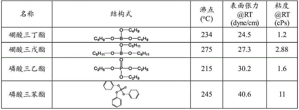
实施例5:含硼酸三戊酯的量子点印刷油墨的制备Embodiment 5: the preparation of quantum dot printing ink containing tripentyl borate
在小瓶内放入搅拌子,清洗干净后转移至手套箱中。在小瓶中配制9.5g硼酸三戊酯溶剂。用丙酮将量子点从溶液中析出,离心得到量子点固体。在手套箱中称取0.5g量子点固体,加到小瓶中的溶剂体系中,搅拌混合。在60℃温度下搅拌直至量子点完全分散后,冷却至室温。将得到的量子点溶液经0.2μm PTFE滤膜过滤。密封并保存。Put a stir bar in the vial, clean it and transfer it to the glove box. Prepare 9.5 g of tripentyl borate solvent in a vial. The quantum dots were precipitated from the solution with acetone and centrifuged to obtain solid quantum dots. Weigh 0.5 g of quantum dot solid in the glove box, add it to the solvent system in the vial, and stir to mix. Stir at 60°C until the quantum dots are completely dispersed, and then cool to room temperature. The resulting quantum dot solution was filtered through a 0.2 μm PTFE filter. Seal and store.
实施例6:含磷酸三苯酯与磷酸三乙酯的量子点印刷油墨的制备Embodiment 6: the preparation of the quantum dot printing ink containing triphenyl phosphate and triethyl phosphate
在小瓶内放入搅拌子,清洗干净后转移至手套箱中。在小瓶中配制9.5g磷酸三苯酯与磷酸三乙酯的混合溶剂(重量比为40:60)。用丙酮将量子点从溶液中析出,离心得到量子点固体。在手套箱中称取0.5g量子点固体,加到小瓶中的溶剂体系中,搅拌混合。在60℃温度下搅拌直至量子点完全分散后,冷却至室温。将得到的量子点溶液经0.2μm PTFE滤膜过滤。密封并保存。Put a stir bar in the vial, clean it and transfer it to the glove box. A mixed solvent (weight ratio of 40:60) of 9.5 g of triphenyl phosphate and triethyl phosphate was prepared in a vial. The quantum dots were precipitated from the solution with acetone and centrifuged to obtain solid quantum dots. Weigh 0.5 g of quantum dot solid in the glove box, add it to the solvent system in the vial, and stir to mix. Stir at 60°C until the quantum dots are completely dispersed, and then cool to room temperature. The resulting quantum dot solution was filtered through a 0.2 μm PTFE filter. Seal and store.
实施例7:含磷酸三乙酯的ZnO纳米粒子印刷油墨的制备Embodiment 7: the preparation of the ZnO nanoparticle printing ink containing triethyl phosphate
在小瓶内放入搅拌子,清洗干净后转移至手套箱中。在小瓶中配制9.5g磷酸三乙酯溶剂。在手套箱中称取0.5g ZnO纳米粒子固体,加到小瓶中的溶剂体系中,搅拌混合。在60℃温度下搅拌直至ZnO纳米粒子完全分散后,冷却至室温。将得到的ZnO纳米粒子溶液经0.2μm PTFE滤膜过滤。密封并保存。Put a stir bar in the vial, clean it and transfer it to the glove box. Prepare 9.5 g of triethyl phosphate solvent in a vial. Weigh 0.5 g of ZnO nanoparticle solid in the glove box, add it to the solvent system in the vial, and stir to mix. Stir at 60°C until the ZnO nanoparticles are completely dispersed, and then cool to room temperature. The resulting ZnO nanoparticle solution was filtered through a 0.2 μm PTFE membrane. Seal and store.
实施例8:含磷酸三苯酯与硼酸三戊酯的ZnO纳米粒子印刷油墨的制备Embodiment 8: the preparation of the ZnO nanoparticle printing ink containing triphenyl phosphate and tripentyl borate
在小瓶内放入搅拌子,清洗干净后转移至手套箱中。在小瓶中配制9.5g磷酸三苯酯与硼酸三戊酯的混合溶剂(重量比为40:60)。在手套箱中称取0.5g ZnO纳米粒子固体,加到小瓶中的溶剂体系中,搅拌混合。在60℃温度下搅拌直至ZnO纳米粒子完全分散后,冷却至室温。将得到的ZnO纳米粒子溶液经0.2μm PTFE滤膜过滤。密封并保存。Put a stir bar in the vial, clean it and transfer it to the glove box. A mixed solvent (weight ratio of 40:60) of 9.5 g of triphenyl phosphate and tripentyl borate was prepared in a vial. Weigh 0.5 g of ZnO nanoparticle solid in the glove box, add it to the solvent system in the vial, and stir to mix. Stir at 60°C until the ZnO nanoparticles are completely dispersed, and then cool to room temperature. The resulting ZnO nanoparticle solution was filtered through a 0.2 μm PTFE membrane. Seal and store.
以下实施例中所涉及的有机功能材料均是可商业购得,如吉林奥莱德(JilinOLED Material Tech Co.,Ltd,www.jl-oled.com),或按照文献报道的方法合成而得。The organic functional materials involved in the following examples are all commercially available, such as Jilin OLED Material Tech Co., Ltd, www.jl-oled.com, or synthesized according to methods reported in the literature.
实施例9:含磷酸三苯酯与硼酸三戊酯的有机发光层材料印刷油墨的制备Embodiment 9: the preparation of organic light-emitting layer material printing ink containing triphenyl phosphate and tripentyl borate
在该实施例中,发光层有机功能材料包含一种磷光主体材料和一种磷光发光体材料。磷光主体材料选自如下的咔唑衍生物:In this embodiment, the organic functional material of the light-emitting layer includes a phosphorescent host material and a phosphorescent emitter material. The phosphorescent host material is selected from the following carbazole derivatives:

磷光发光体材料选自如下铱配合物:The phosphorescent emitter material is selected from the following iridium complexes:
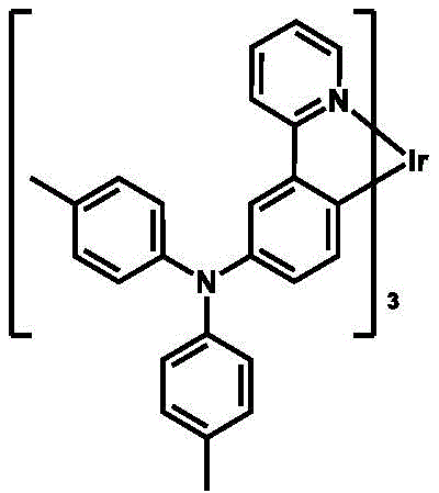
在小瓶内放入搅拌子,清洗干净后转移至手套箱中。在小瓶中配制9.8g磷酸三苯酯与硼酸三戊酯的混合溶剂(重量比为40:60)。在手套箱中称取0.18g磷光主体材料和0.02g磷光发光体材料,加到小瓶中的溶剂体系中,搅拌混合。在60℃温度下搅拌直至有机功能材料完全溶解后,冷却至室温。将得到的有机功能材料溶液经0.2μm PTFE滤膜过滤。密封并保存。Put a stir bar in the vial, clean it and transfer it to the glove box. A mixed solvent (weight ratio of 40:60) of 9.8 g of triphenyl phosphate and tripentyl borate was prepared in a vial. Weigh 0.18 g of the phosphorescent host material and 0.02 g of the phosphorescent emitter material in the glove box, add them to the solvent system in the vial, and stir and mix. After stirring at 60°C until the organic functional material is completely dissolved, it was cooled to room temperature. The resulting organic functional material solution was filtered through a 0.2 μm PTFE membrane. Seal and store.
实施例10:含磷酸三苯酯与磷酸三乙酯的有机发光层材料印刷油墨的制备Embodiment 10: the preparation of organic light-emitting layer material printing ink containing triphenyl phosphate and triethyl phosphate
在该实施例中,发光层有机功能材料包含一种荧光主体材料和一种荧光发光体材料。In this embodiment, the organic functional material of the light-emitting layer includes a fluorescent host material and a fluorescent emitter material.
荧光主体材料选自如下的螺芴衍生物:The fluorescent host material is selected from the following spirofluorene derivatives:

荧光发光体材料选自如下化合物:The fluorescent emitter material is selected from the following compounds:

在小瓶内放入搅拌子,清洗干净后转移至手套箱中。在小瓶中配制9.8g磷酸三苯酯与磷酸三乙酯的混合溶剂(重量比为40:60)。在手套箱中称取0.19g荧光主体材料和0.01g荧光发光体材料,加到小瓶中的溶剂体系中,搅拌混合。在60℃温度下搅拌直至有机功能材料完全溶解后,冷却至室温。将得到的有机功能材料溶液经0.2μm PTFE滤膜过滤。密封并保存。Put a stir bar in the vial, clean it and transfer it to the glove box. A mixed solvent of 9.8 g of triphenyl phosphate and triethyl phosphate (40:60 by weight) was prepared in a vial. In the glove box, weigh 0.19 g of the fluorescent host material and 0.01 g of the fluorescent light-emitting body material, add them to the solvent system in the vial, and stir and mix. After stirring at 60°C until the organic functional material is completely dissolved, it was cooled to room temperature. The resulting organic functional material solution was filtered through a 0.2 μm PTFE membrane. Seal and store.
实施例11:含磷酸三苯酯与磷酸三乙酯的有机发光层材料印刷油墨的制备Embodiment 11: the preparation of organic light-emitting layer material printing ink containing triphenyl phosphate and triethyl phosphate
在该实施例中,发光层有机功能材料包含一种主体材料和一种TADF材料。In this embodiment, the organic functional material of the light-emitting layer includes a host material and a TADF material.
主体材料选自如下结构的化合物:The host material is selected from compounds of the following structures:
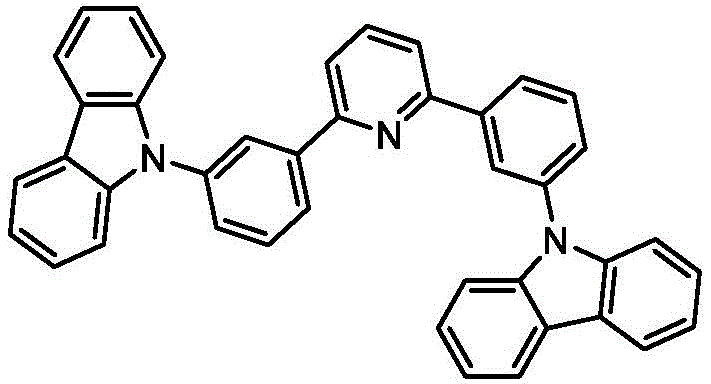
TADF材料选自如下结构的化合物:TADF materials are selected from compounds of the following structures:

在小瓶内放入搅拌子,清洗干净后转移至手套箱中。在小瓶中配制9.8g磷酸三苯酯与磷酸三乙酯的混合溶剂(重量比为40:60)。在手套箱中称取0.19g主体材料和0.01gTADF材料,加到小瓶中的溶剂体系中,搅拌混合。在60℃温度下搅拌直至有机功能材料完全溶解后,冷却至室温。将得到的有机功能材料溶液经0.2μm PTFE滤膜过滤。密封并保存Put a stir bar in the vial, clean it and transfer it to the glove box. A mixed solvent of 9.8 g of triphenyl phosphate and triethyl phosphate (40:60 by weight) was prepared in a vial. Weigh 0.19 g of the host material and 0.01 g of the TADF material in the glove box, add them to the solvent system in the vial, and stir to mix. After stirring at 60°C until the organic functional material is completely dissolved, it was cooled to room temperature. The resulting organic functional material solution was filtered through a 0.2 μm PTFE membrane. seal and save
实施例12:含磷酸三苯酯和硼酸三丁酯的空穴传输材料印刷油墨的制备Example 12: Preparation of hole transport material printing ink containing triphenyl phosphate and tributyl borate
在该实施例中,印刷油墨包含一种具有空穴传输能力的空穴传输层材料。In this embodiment, the printing ink includes a hole transport layer material having hole transport capabilities.
空穴传输材料选自如下的三芳胺衍生物:The hole transport material is selected from the following triarylamine derivatives:

在小瓶内放入搅拌子,清洗干净后转移至手套箱中。在小瓶中配制9.8g磷酸三苯酯与硼酸三丁酯的混合溶剂(重量比为40:60)。在手套箱中称取0.2g空穴传输材料,加到小瓶中的溶剂体系中,搅拌混合。在60℃温度下搅拌直至有机功能材料完全溶解后,冷却至室温。将得到的有机功能材料溶液经0.2μm PTFE滤膜过滤。密封并保存。Put a stir bar in the vial, clean it and transfer it to the glove box. A mixed solvent (weight ratio of 40:60) of 9.8 g of triphenyl phosphate and tributyl borate was prepared in a vial. Weigh 0.2 g of hole transport material in the glove box, add it to the solvent system in the vial, and stir to mix. After stirring at 60°C until the organic functional material is completely dissolved, it was cooled to room temperature. The resulting organic functional material solution was filtered through a 0.2 μm PTFE membrane. Seal and store.
实施例13:粘度及表面张力测试Example 13: Viscosity and Surface Tension Testing
功能材料油墨的粘度由DV-I Prime Brookfield流变仪测试;功能材料油墨的表面张力由SITA气泡压力张力仪测试。The viscosity of functional material ink was tested by DV-I Prime Brookfield rheometer; the surface tension of functional material ink was tested by SITA bubble pressure tensiometer.
经上述测试,实施例5得到的功能材料油墨的粘度为3.8±0.5cPs,表面张力为26.9±0.5dyne/cm。After the above test, the viscosity of the functional material ink obtained in Example 5 is 3.8±0.5cPs, and the surface tension is 26.9±0.5dyne/cm.
经上述测试,实施例6得到的功能材料油墨的粘度为4.7±0.5cPs,表面张力为33.6±0.3dyne/cm。After the above test, the viscosity of the functional material ink obtained in Example 6 is 4.7±0.5cPs, and the surface tension is 33.6±0.3dyne/cm.
经上述测试,实施例7得到的功能材料油墨的粘度为2.9±0.5cPs,表面张力为29.5±0.5dyne/cm。After the above test, the viscosity of the functional material ink obtained in Example 7 is 2.9±0.5cPs, and the surface tension is 29.5±0.5dyne/cm.
经上述测试,实施例8得到的功能材料油墨的粘度为6.3±0.5cPs,表面张力为32.3±0.3dyne/cm。After the above tests, the viscosity of the functional material ink obtained in Example 8 was 6.3±0.5 cPs, and the surface tension was 32.3±0.3 dyne/cm.
经上述测试,实施例9得到的功能材料油墨的粘度为6.1±0.5cPs,表面张力为32.7±0.5dyne/cm。After the above test, the viscosity of the functional material ink obtained in Example 9 was 6.1±0.5 cPs, and the surface tension was 32.7±0.5 dyne/cm.
经上述测试,实施例10得到的功能材料油墨的粘度为4.9±0.5cPs,表面张力为32.4±0.3dyne/cm。After the above test, the viscosity of the functional material ink obtained in Example 10 was 4.9±0.5 cPs, and the surface tension was 32.4±0.3 dyne/cm.
经上述测试,实施例11得到的功能材料油墨的粘度为5.1±0.5cPs,表面张力为32.6±0.5dyne/cm。After the above test, the viscosity of the functional material ink obtained in Example 11 was 5.1±0.5 cPs, and the surface tension was 32.6±0.5 dyne/cm.
经上述测试,实施例12得到的功能材料油墨的粘度为4.4±0.5cPs,表面张力为28.4±0.5dyne/cm。After the above test, the viscosity of the functional material ink obtained in Example 12 was 4.4±0.5 cPs, and the surface tension was 28.4±0.5 dyne/cm.
利用上述制备的基于无机酯溶剂体系的包含功能材料的印刷油墨,通过喷墨打印的方式,可制备发光二极管中的功能层,如发光层和电荷传输层,具体步骤如下。Using the above-prepared printing ink containing functional materials based on an inorganic ester solvent system, functional layers in light-emitting diodes, such as light-emitting layers and charge transport layers, can be prepared by means of inkjet printing. The specific steps are as follows.
将包含功能材料的油墨装入油墨桶中,油墨桶装配于喷墨打印机,如DimatixMaterials Printer DMP-3000(Fujifilm)。调节喷射油墨的波形、脉冲时间和电压,使油墨喷射达到最优,且实现油墨喷射范围的稳定化。在制备功能材料薄膜为发光层的OLED/QLED器件时,按照如下技术方案:OLED/QLED的基板为溅射有氧化铟锡(ITO)电极图案的0.7mm厚的玻璃。在ITO上使像素界定层图案话,形成内部用于沉积打印油墨的孔。然后将HIL/HTL材料喷墨打印至该孔中,真空环境下高温干燥移除溶剂,得到HIL/HTL薄膜。此后,将包含发光功能材料的印刷油墨喷墨打印到HIL/HTL薄膜上,真空环境下高温干燥移除溶剂,得到发光层薄膜。随后将包含电子传输性能的功能材料的印刷油墨喷墨打印到发光层薄膜上,真空环境下高温干燥移除溶剂,形成电子传输层(ETL)。在使用有机电子传输材料时,ETL也可通过真空热蒸镀而成。然后Al阴极通过真空热蒸镀而成,最后封装完成OLED/QLED器件制备。The ink containing the functional material is charged into an ink tank, which is fitted to an ink jet printer, such as a Dimatix Materials Printer DMP-3000 (Fujifilm). Adjust the waveform, pulse time and voltage of the jetting ink to optimize the ink jetting and achieve the stabilization of the ink jetting range. When preparing the OLED/QLED device with the functional material thin film as the light-emitting layer, the following technical scheme is used: the substrate of the OLED/QLED is a 0.7 mm thick glass sputtered with an indium tin oxide (ITO) electrode pattern. A pixel-defining layer was patterned on the ITO to form holes inside for the deposition of printing ink. Then, the HIL/HTL material was ink-jet printed into the hole, and the solvent was removed by drying at high temperature in a vacuum environment to obtain a HIL/HTL film. After that, the printing ink containing the light-emitting functional material is ink-jet printed on the HIL/HTL film, and the solvent is removed by drying at a high temperature in a vacuum environment to obtain a light-emitting layer film. Then, the printing ink containing the functional material with electron transport properties is inkjet printed on the light-emitting layer thin film, and the solvent is removed by drying at high temperature in a vacuum environment to form an electron transport layer (ETL). When using organic electron transport materials, ETL can also be formed by vacuum thermal evaporation. Then the Al cathode is formed by vacuum thermal evaporation, and finally the OLED/QLED device is prepared by encapsulation.
Claims (15)

Applications Claiming Priority (3)
| Application Number | Priority Date | Filing Date | Title |
|---|---|---|---|
| CN2015107694709 | 2015-11-12 | ||
| CN201510769470 | 2015-11-12 | ||
| PCT/CN2016/100164 WO2017080326A1 (en) | 2015-11-12 | 2016-09-26 | Printing composition, electronic device comprising same and preparation method for functional material thin film |
Publications (2)
| Publication Number | Publication Date |
|---|---|
| CN108291103A CN108291103A (en) | 2018-07-17 |
| CN108291103B true CN108291103B (en) | 2021-12-07 |
Family
ID=58694697
Family Applications (1)
| Application Number | Title | Priority Date | Filing Date |
|---|---|---|---|
| CN201680059877.5A Active CN108291103B (en) | 2015-11-12 | 2016-09-26 | Printing composition, electronic device comprising same and preparation method of functional material film |
Country Status (3)
| Country | Link |
|---|---|
| US (1) | US11555128B2 (en) |
| CN (1) | CN108291103B (en) |
| WO (1) | WO2017080326A1 (en) |
Families Citing this family (8)
| Publication number | Priority date | Publication date | Assignee | Title |
|---|---|---|---|---|
| JP7048250B2 (en) * | 2017-10-19 | 2022-04-05 | 住友化学株式会社 | Manufacturing method of organic electronic devices |
| CN108300455A (en) * | 2018-01-29 | 2018-07-20 | 福州大学 | A kind of colorful polymer composite film and preparation method thereof based on perovskite quantum dot |
| CN108767129B (en) * | 2018-05-31 | 2021-01-26 | 京东方科技集团股份有限公司 | Quantum dot light-emitting diode, its preparation method, and display panel |
| KR20220085925A (en) * | 2020-12-15 | 2022-06-23 | 삼성디스플레이 주식회사 | Electron transporting layer ink composition for light emitting device and light emitting device made with same |
| KR20220095392A (en) * | 2020-12-29 | 2022-07-07 | 삼성디스플레이 주식회사 | Nanoparticle ink composition, light emitting device, and method for manufacturing the same |
| US12213331B2 (en) | 2021-01-29 | 2025-01-28 | The Regents Of The University Of Michigan | Hybrid organic-inorganic light emitting device |
| JP2023012818A (en) * | 2021-07-14 | 2023-01-26 | 三菱ケミカル株式会社 | Composition for forming light emitting layer of quantum dot light emitting element, quantum dot light emitting element, quantum dot display device, and quantum dot lighting |
| CN115333497A (en) * | 2022-06-28 | 2022-11-11 | 广州市艾佛光通科技有限公司 | Preparation method of film cavity acoustic wave resonator and film cavity acoustic wave resonator |
Citations (6)
| Publication number | Priority date | Publication date | Assignee | Title |
|---|---|---|---|---|
| CN1682573A (en) * | 2002-09-17 | 2005-10-12 | 国际商业机器公司 | Organic electroluminescent display and method for manufacturing organic electroluminescent display |
| CN101796621A (en) * | 2007-09-03 | 2010-08-04 | 富士胶片株式会社 | Method for preparing single crystal thin film of organic semiconducting compound |
| KR20110100965A (en) * | 2010-03-05 | 2011-09-15 | 삼성전자주식회사 | Scent cell array substrate, olfactory information transfer device, and electronic device |
| CN102916097A (en) * | 2011-08-01 | 2013-02-06 | 潘才法 | Electroluminescent device |
| CN103958623A (en) * | 2011-10-04 | 2014-07-30 | 惠普发展公司,有限责任合伙企业 | An ink composition |
| CN105038408A (en) * | 2015-08-14 | 2015-11-11 | 广州华睿光电材料有限公司 | Printing ink and electronic device printed by applying printing ink |
Family Cites Families (144)
| Publication number | Priority date | Publication date | Assignee | Title |
|---|---|---|---|---|
| US3567450A (en) | 1968-02-20 | 1971-03-02 | Eastman Kodak Co | Photoconductive elements containing substituted triarylamine photoconductors |
| US3615404A (en) | 1968-04-25 | 1971-10-26 | Scott Paper Co | 1 3-phenylenediamine containing photoconductive materials |
| US4720432A (en) | 1987-02-11 | 1988-01-19 | Eastman Kodak Company | Electroluminescent device with organic luminescent medium |
| US4769292A (en) | 1987-03-02 | 1988-09-06 | Eastman Kodak Company | Electroluminescent device with modified thin film luminescent zone |
| US5121029A (en) | 1987-12-11 | 1992-06-09 | Idemitsu Kosan Co., Ltd. | Electroluminescence device having an organic electroluminescent element |
| US5130603A (en) | 1989-03-20 | 1992-07-14 | Idemitsu Kosan Co., Ltd. | Organic electroluminescence device |
| US5061569A (en) | 1990-07-26 | 1991-10-29 | Eastman Kodak Company | Electroluminescent device with organic electroluminescent medium |
| JP2913116B2 (en) | 1990-11-20 | 1999-06-28 | 株式会社リコー | EL device |
| US5708130A (en) | 1995-07-28 | 1998-01-13 | The Dow Chemical Company | 2,7-aryl-9-substituted fluorenes and 9-substituted fluorene oligomers and polymers |
| EP1146034A1 (en) | 1995-09-25 | 2001-10-17 | Toyo Ink Manufacturing Co., Ltd. | Light-emitting material for organic electroluminescence device, and organic electroluminescence device for which the light-emitting material is adapted |
| US6322901B1 (en) | 1997-11-13 | 2001-11-27 | Massachusetts Institute Of Technology | Highly luminescent color-selective nano-crystalline materials |
| US6607829B1 (en) | 1997-11-13 | 2003-08-19 | Massachusetts Institute Of Technology | Tellurium-containing nanocrystalline materials |
| US6830828B2 (en) | 1998-09-14 | 2004-12-14 | The Trustees Of Princeton University | Organometallic complexes as phosphorescent emitters in organic LEDs |
| US6251303B1 (en) | 1998-09-18 | 2001-06-26 | Massachusetts Institute Of Technology | Water-soluble fluorescent nanocrystals |
| US6426513B1 (en) | 1998-09-18 | 2002-07-30 | Massachusetts Institute Of Technology | Water-soluble thiol-capped nanocrystals |
| US6020078A (en) | 1998-12-18 | 2000-02-01 | Eastman Kodak Company | Green organic electroluminescent devices |
| WO2000070655A2 (en) | 1999-05-13 | 2000-11-23 | The Trustees Of Princeton University | Very high efficiency organic light emitting devices based on electrophosphorescence |
| GB9920543D0 (en) | 1999-08-31 | 1999-11-03 | Cambridge Display Tech Ltd | A formulation for depositing a light-emitting polymer layer |
| KR100799799B1 (en) | 1999-09-21 | 2008-02-01 | 이데미쓰 고산 가부시키가이샤 | Organic Electroluminescent Devices and Organic Light Emitting Media |
| KR100946314B1 (en) | 1999-12-01 | 2010-03-09 | 더 트러스티즈 오브 프린스턴 유니버시티 | Organic light emitting device comprising a phosphorescent organo metallic compound |
| JP4951184B2 (en) | 2000-03-20 | 2012-06-13 | マサチューセッツ インスティテュート オブ テクノロジー | Inorganic particle conjugate |
| JP4048521B2 (en) | 2000-05-02 | 2008-02-20 | 富士フイルム株式会社 | Light emitting element |
| US20020121638A1 (en) | 2000-06-30 | 2002-09-05 | Vladimir Grushin | Electroluminescent iridium compounds with fluorinated phenylpyridines, phenylpyrimidines, and phenylquinolines and devices made with such compounds |
| CN101924190B (en) | 2000-08-11 | 2012-07-04 | 普林斯顿大学理事会 | Organometallic compounds and emission-shifting organic electrophosphorescence |
| JP4154138B2 (en) | 2000-09-26 | 2008-09-24 | キヤノン株式会社 | Light emitting element, display device and metal coordination compound |
| JP4154140B2 (en) | 2000-09-26 | 2008-09-24 | キヤノン株式会社 | Metal coordination compounds |
| JP4154139B2 (en) | 2000-09-26 | 2008-09-24 | キヤノン株式会社 | Light emitting element |
| US6576291B2 (en) | 2000-12-08 | 2003-06-10 | Massachusetts Institute Of Technology | Preparation of nanocrystallites |
| CN1271041C (en) | 2001-03-16 | 2006-08-23 | 出光兴产株式会社 | Process for producing aromatic amino compound |
| US7250226B2 (en) | 2001-08-31 | 2007-07-31 | Nippon Hoso Kyokai | Phosphorescent compound, a phosphorescent composition and an organic light-emitting device |
| JP4629643B2 (en) | 2001-08-31 | 2011-02-09 | 日本放送協会 | Organic light emitting device and display device |
| DE10143353A1 (en) | 2001-09-04 | 2003-03-20 | Covion Organic Semiconductors | Conjugated polymers containing spirobifluorene units and their use |
| US6835469B2 (en) | 2001-10-17 | 2004-12-28 | The University Of Southern California | Phosphorescent compounds and devices comprising the same |
| US7150910B2 (en) | 2001-11-16 | 2006-12-19 | Massachusetts Institute Of Technology | Nanocrystal structures |
| US6686065B2 (en) | 2001-12-12 | 2004-02-03 | Canon Kabushiki Kaisha | [5]-helicene and dibenzofluorene materials for use in organic light emitting devices |
| JP4256182B2 (en) | 2002-03-14 | 2009-04-22 | Tdk株式会社 | Organic EL device |
| DE10211648A1 (en) | 2002-03-15 | 2003-09-25 | Basf Ag | Polymers based on fluoranthene and their use |
| SG128438A1 (en) | 2002-03-15 | 2007-01-30 | Sumitomo Chemical Co | Polymer compound and polymer light emitting deviceusing the same |
| TWI314947B (en) | 2002-04-24 | 2009-09-21 | Eastman Kodak Compan | Organic light emitting diode devices with improved operational stability |
| CA2485945C (en) | 2002-05-15 | 2011-01-18 | Yissum Research Development Company Of The Hebrew University Of Jerusalem | Method for producing inorganic semiconductor nanocrystalline rods and their use |
| AU2003241788A1 (en) | 2002-05-28 | 2003-12-12 | Sumitomo Chemical Company, Limited | Polymer and polymeric luminescent element comprising the same |
| US7534488B2 (en) | 2003-09-10 | 2009-05-19 | The Regents Of The University Of California | Graded core/shell semiconductor nanorods and nanorod barcodes |
| GB0226010D0 (en) | 2002-11-08 | 2002-12-18 | Cambridge Display Tech Ltd | Polymers for use in organic electroluminescent devices |
| EP1590171B1 (en) | 2003-01-22 | 2011-06-08 | The Board Of Trustees Of The University Of Arkansas | Monodisperse core/shell and other complex structured nanocrystals and methods of preparing the same |
| EP1491568A1 (en) | 2003-06-23 | 2004-12-29 | Covion Organic Semiconductors GmbH | Semiconductive Polymers |
| DE10338550A1 (en) | 2003-08-19 | 2005-03-31 | Basf Ag | Transition metal complexes with carbene ligands as emitters for organic light-emitting diodes (OLEDs) |
| DE10345572A1 (en) | 2003-09-29 | 2005-05-19 | Covion Organic Semiconductors Gmbh | metal complexes |
| JP2005108556A (en) | 2003-09-29 | 2005-04-21 | Tdk Corp | Organic el element and organic el display |
| DE112004001856T5 (en) | 2003-10-01 | 2006-07-27 | Sumitomo Chemical Co., Ltd. | Light emitting polymer material and light emitting polymeric device |
| US7029766B2 (en) | 2003-12-05 | 2006-04-18 | Eastman Kodak Company | Organic element for electroluminescent devices |
| US6824895B1 (en) | 2003-12-05 | 2004-11-30 | Eastman Kodak Company | Electroluminescent device containing organometallic compound with tridentate ligand |
| TW200530373A (en) | 2003-12-12 | 2005-09-16 | Sumitomo Chemical Co | Polymer and light-emitting element using said polymer |
| JP4466160B2 (en) | 2004-03-30 | 2010-05-26 | Tdk株式会社 | Organic EL element and organic EL display |
| DE102004020298A1 (en) | 2004-04-26 | 2005-11-10 | Covion Organic Semiconductors Gmbh | Electroluminescent polymers and their use |
| US7598388B2 (en) | 2004-05-18 | 2009-10-06 | The University Of Southern California | Carbene containing metal complexes as OLEDs |
| CN100368363C (en) | 2004-06-04 | 2008-02-13 | 友达光电股份有限公司 | Anthracene compound and organic electroluminescent device comprising the same |
| KR100658993B1 (en) | 2004-06-22 | 2006-12-21 | 학교법인 포항공과대학교 | Semiconductor nanorods surface-treated with polymer |
| TW200613515A (en) | 2004-06-26 | 2006-05-01 | Merck Patent Gmbh | Compounds for organic electronic devices |
| DE102004031000A1 (en) | 2004-06-26 | 2006-01-12 | Covion Organic Semiconductors Gmbh | Organic electroluminescent devices |
| DE102004034517A1 (en) | 2004-07-16 | 2006-02-16 | Covion Organic Semiconductors Gmbh | metal complexes |
| US20060094859A1 (en) | 2004-11-03 | 2006-05-04 | Marrocco Matthew L Iii | Class of bridged biphenylene polymers |
| TW200639140A (en) | 2004-12-01 | 2006-11-16 | Merck Patent Gmbh | Compounds for organic electronic devices |
| TWI385193B (en) | 2004-12-07 | 2013-02-11 | Sumitomo Chemical Co | Polymer material and components using the same |
| JP4263700B2 (en) | 2005-03-15 | 2009-05-13 | 出光興産株式会社 | Aromatic amine derivative and organic electroluminescence device using the same |
| US20060222886A1 (en) | 2005-04-04 | 2006-10-05 | Raymond Kwong | Arylpyrene compounds |
| DE102005019880A1 (en) | 2005-04-28 | 2006-11-09 | Basf Ag | Synthesis of phenyl-substituted polyfluoranthenes and their use |
| CN101184789B (en) | 2005-04-28 | 2012-05-30 | 住友化学株式会社 | High-molecular compound and high-molecular luminescent device using the same |
| DE102005023437A1 (en) | 2005-05-20 | 2006-11-30 | Merck Patent Gmbh | Connections for organic electronic devices |
| JP5137825B2 (en) | 2005-06-15 | 2013-02-06 | イッサム リサーチ デベロップメント カンパニー オブ ザ ヘブライ ユニバーシティ オブ エルサレム | III-V semiconductor core-heteroshell nanocrystal |
| US20070009275A1 (en) | 2005-06-24 | 2007-01-11 | Olympus Corporation | Image forming apparatus |
| GB2445519B (en) | 2005-10-07 | 2010-11-24 | Sumitomo Chemical Co | Copolymer and polymer light emitting device using the same |
| US7588839B2 (en) | 2005-10-19 | 2009-09-15 | Eastman Kodak Company | Electroluminescent device |
| DE102005058543A1 (en) | 2005-12-08 | 2007-06-14 | Merck Patent Gmbh | Organic electroluminescent devices |
| DE102005058557A1 (en) | 2005-12-08 | 2007-06-14 | Merck Patent Gmbh | Organic electroluminescent device |
| JP4879591B2 (en) | 2006-01-26 | 2012-02-22 | 昭和電工株式会社 | Polymer light-emitting material, organic electroluminescence element, and display device |
| US7972694B2 (en) | 2006-01-30 | 2011-07-05 | Konica Minolta Medical & Graphic, Inc. | Triple-layer semiconductor nanoparticle and triple-layer semiconductor nanorod |
| US8835941B2 (en) | 2006-02-09 | 2014-09-16 | Qd Vision, Inc. | Displays including semiconductor nanocrystals and methods of making same |
| KR101600624B1 (en) | 2006-02-10 | 2016-03-21 | 유니버셜 디스플레이 코포레이션 | METAL COMPLEXES OF CYCLOMETALLATED IMIDAZO[1,2-f]PHENANTHRIDINE AND DIIMIDAZO[1,2-A:1',2'-C]QUINAZOLINE LIGANDS AND ISOELECTRONIC AND BENZANNULATED ANALOGS THEREOF |
| US20070208567A1 (en) | 2006-03-01 | 2007-09-06 | At&T Corp. | Error Correction In Automatic Speech Recognition Transcripts |
| WO2007143197A2 (en) | 2006-06-02 | 2007-12-13 | Qd Vision, Inc. | Light-emitting devices and displays with improved performance |
| WO2008070028A2 (en) | 2006-12-01 | 2008-06-12 | Qd Vision, Inc. | Improved composites and devices including nanoparticles |
| KR100744351B1 (en) | 2006-03-24 | 2007-07-30 | 삼성전자주식회사 | UV emitting ink and security device using same |
| DE102006015183A1 (en) | 2006-04-01 | 2007-10-04 | Merck Patent Gmbh | Materials for organic electroluminescent devices |
| WO2007117672A2 (en) | 2006-04-07 | 2007-10-18 | Qd Vision, Inc. | Methods of depositing nanomaterial & methods of making a device |
| WO2007120877A2 (en) | 2006-04-14 | 2007-10-25 | Qd Vision, Inc. | Transfer surface for manufacturing a light emitting device |
| US20070252517A1 (en) | 2006-04-27 | 2007-11-01 | Eastman Kodak Company | Electroluminescent device including an anthracene derivative |
| US20080277626A1 (en) * | 2006-05-23 | 2008-11-13 | Evident Technologies, Inc. | Quantum dot fluorescent inks |
| DE102006025846A1 (en) | 2006-06-02 | 2007-12-06 | Merck Patent Gmbh | New materials for organic electroluminescent devices |
| WO2008111947A1 (en) | 2006-06-24 | 2008-09-18 | Qd Vision, Inc. | Methods and articles including nanomaterial |
| WO2008108798A2 (en) | 2006-06-24 | 2008-09-12 | Qd Vision, Inc. | Methods for depositing nanomaterial, methods for fabricating a device, and methods for fabricating an array of devices |
| WO2008105792A2 (en) | 2006-06-24 | 2008-09-04 | Qd Vision, Inc. | Methods for depositing nanomaterial, methods for fabricating a device, methods for fabricating an array of devices and compositions |
| DE102006031990A1 (en) | 2006-07-11 | 2008-01-17 | Merck Patent Gmbh | New materials for organic electroluminescent devices |
| JP2008053397A (en) | 2006-08-24 | 2008-03-06 | Ricoh Co Ltd | Semiconductor device and manufacturing method thereof |
| WO2008033388A2 (en) | 2006-09-12 | 2008-03-20 | Qd Vision, Inc. | A composite including nanoparticles, methods, and products including a composite |
| JP2010508620A (en) | 2006-09-12 | 2010-03-18 | キユーデイー・ビジヨン・インコーポレーテツド | Electroluminescent display useful for displaying a predetermined pattern |
| JP2008124156A (en) | 2006-11-09 | 2008-05-29 | Idemitsu Kosan Co Ltd | Organic EL material-containing solution, organic EL material thin film formation method, organic EL material thin film, organic EL element |
| WO2008063653A1 (en) | 2006-11-21 | 2008-05-29 | Qd Vision, Inc. | Semiconductor nanocrystals and compositions and devices including same |
| WO2008063652A1 (en) | 2006-11-21 | 2008-05-29 | Qd Vision, Inc. | Blue emitting semiconductor nanocrystals and compositions and devices including same |
| US8836212B2 (en) | 2007-01-11 | 2014-09-16 | Qd Vision, Inc. | Light emissive printed article printed with quantum dot ink |
| JP4902381B2 (en) | 2007-02-07 | 2012-03-21 | 昭和電工株式会社 | Polymer of polymerizable compound |
| WO2009014590A2 (en) | 2007-06-25 | 2009-01-29 | Qd Vision, Inc. | Compositions and methods including depositing nanomaterial |
| US20090130296A1 (en) | 2007-11-15 | 2009-05-21 | Universal Display Corporation | Fabrication of Organic Electronic Devices by Ink-Jet Printing at Low Temperatures |
| WO2009068878A2 (en) | 2007-11-30 | 2009-06-04 | Nanoco Technologies Limited | Preparation of nanoparticle material |
| US8221905B2 (en) | 2007-12-28 | 2012-07-17 | Universal Display Corporation | Carbazole-containing materials in phosphorescent light emitting diodes |
| KR101475520B1 (en) | 2008-01-14 | 2014-12-23 | 삼성전자주식회사 | Quantum dot ink composition for inkjet printing and electronic device using the same |
| DE102008015526B4 (en) | 2008-03-25 | 2021-11-11 | Merck Patent Gmbh | Metal complexes |
| DE102008027005A1 (en) | 2008-06-05 | 2009-12-10 | Merck Patent Gmbh | Organic electronic device containing metal complexes |
| GB2462410B (en) | 2008-07-21 | 2011-04-27 | Cambridge Display Tech Ltd | Compositions and methods for manufacturing light-emissive devices |
| DE102008036247A1 (en) | 2008-08-04 | 2010-02-11 | Merck Patent Gmbh | Electronic devices containing metal complexes |
| DE102008048336A1 (en) | 2008-09-22 | 2010-03-25 | Merck Patent Gmbh | Mononuclear neutral copper (I) complexes and their use for the production of optoelectronic devices |
| DE102008057050B4 (en) | 2008-11-13 | 2021-06-02 | Merck Patent Gmbh | Materials for organic electroluminescent devices |
| DE102008057051B4 (en) | 2008-11-13 | 2021-06-17 | Merck Patent Gmbh | Materials for organic electroluminescent devices |
| DE102009007038A1 (en) | 2009-02-02 | 2010-08-05 | Merck Patent Gmbh | metal complexes |
| US8174000B2 (en) | 2009-02-11 | 2012-05-08 | Universal Display Corporation | Liquid compositions for inkjet printing of organic layers or other uses |
| DE102009011223A1 (en) | 2009-03-02 | 2010-09-23 | Merck Patent Gmbh | metal complexes |
| DE102009013041A1 (en) | 2009-03-13 | 2010-09-16 | Merck Patent Gmbh | Materials for organic electroluminescent devices |
| US20100264371A1 (en) * | 2009-03-19 | 2010-10-21 | Nick Robert J | Composition including quantum dots, uses of the foregoing, and methods |
| US8586203B2 (en) | 2009-05-20 | 2013-11-19 | Universal Display Corporation | Metal complexes with boron-nitrogen heterocycle containing ligands |
| DE102009023154A1 (en) | 2009-05-29 | 2011-06-16 | Merck Patent Gmbh | A composition comprising at least one emitter compound and at least one polymer having conjugation-interrupting units |
| DE102009023156A1 (en) | 2009-05-29 | 2010-12-02 | Merck Patent Gmbh | Polymers containing substituted indenofluorene derivatives as a structural unit, process for their preparation and their use |
| WO2011110277A1 (en) | 2010-03-11 | 2011-09-15 | Merck Patent Gmbh | Fibers in therapy and cosmetics |
| DE112011102008B4 (en) | 2010-06-15 | 2022-04-21 | Merck Patent Gmbh | metal complexes |
| EP2404627A1 (en) | 2010-07-09 | 2012-01-11 | Universite De Nantes I | Bone regeneration membrane and method for forming a bone regeneration membrane |
| DE102010027319A1 (en) | 2010-07-16 | 2012-01-19 | Merck Patent Gmbh | metal complexes |
| DE102010027317A1 (en) | 2010-07-16 | 2012-01-19 | Merck Patent Gmbh | metal complexes |
| DE102010027316A1 (en) | 2010-07-16 | 2012-01-19 | Merck Patent Gmbh | metal complexes |
| US8956740B2 (en) | 2010-08-24 | 2015-02-17 | Seiko Epson Corporation | Film-forming ink, film-forming method, liquid droplet discharging device, method for preparing light-emitting element, light-emitting element, light-emitting device and electronic apparatus |
| US9783734B2 (en) | 2011-02-28 | 2017-10-10 | Kyulux, Inc. | Delayed fluorescence material and organic electroluminescence device |
| US9660198B2 (en) | 2011-07-15 | 2017-05-23 | Kyulux, Inc. | Organic electroluminescence element and compound used therein |
| JP5875011B2 (en) | 2011-07-15 | 2016-03-02 | 国立大学法人九州大学 | Delayed fluorescent material and organic electroluminescence device using the same |
| US9331295B2 (en) | 2011-12-20 | 2016-05-03 | Seiko Epson Corporation | Film-forming ink, film-forming method, method of manufacturing light emitting element, light emitting element, light emitting device, and electronic apparatus |
| WO2013122820A1 (en) | 2012-02-15 | 2013-08-22 | Qd Vision, Inc. | Method of processing quantum dot inks |
| JP6095643B2 (en) | 2012-03-09 | 2017-03-15 | 株式会社Kyulux | Luminescent material and organic light emitting device |
| JP2014135466A (en) | 2012-04-09 | 2014-07-24 | Kyushu Univ | Organic light emitting element, and light emitting material and compound used in the same |
| KR20150016242A (en) | 2012-04-25 | 2015-02-11 | 고쿠리쓰다이가쿠호진 규슈다이가쿠 | Light-emitting material and organic light-emitting element |
| JP5594750B2 (en) | 2012-05-17 | 2014-09-24 | 国立大学法人九州大学 | COMPOUND, LIGHT EMITTING MATERIAL AND ORGANIC LIGHT EMITTING DEVICE |
| US9252363B2 (en) | 2012-10-04 | 2016-02-02 | Universal Display Corporation | Aryloxyalkylcarboxylate solvent compositions for inkjet printing of organic layers |
| JP6225413B2 (en) | 2012-11-16 | 2017-11-08 | セイコーエプソン株式会社 | Functional layer forming ink, ink container, ejection device, functional layer forming method, organic EL element manufacturing method |
| CN105431910B (en) | 2013-08-12 | 2018-03-06 | 科迪华公司 | Ester-based solvent systems for printable organic light-emitting diode ink formulations |
| CN103483332B (en) | 2013-09-11 | 2016-08-10 | 中山大学 | Piezoluminescent material with thermally activated delayed fluorescence and aggregation-induced luminescent properties, its synthesis method and application |
| US9960314B2 (en) | 2013-09-13 | 2018-05-01 | Nanoco Technologies Ltd. | Inorganic salt-nanoparticle ink for thin film photovoltaic devices and related methods |
| GB2520384A (en) | 2013-09-13 | 2015-05-20 | Nanoco Technologies Ltd | Quantum dot ink formulation for heat transfer printing applications |
| US9893220B2 (en) | 2013-10-15 | 2018-02-13 | Nanoco Technologies Ltd. | CIGS nanoparticle ink formulation having a high crack-free limit |
| CN105062193B (en) * | 2015-08-14 | 2020-01-31 | 广州华睿光电材料有限公司 | Printing ink composition and electronic device |
-
2016
- 2016-09-26 CN CN201680059877.5A patent/CN108291103B/en active Active
- 2016-09-26 US US15/775,395 patent/US11555128B2/en active Active
- 2016-09-26 WO PCT/CN2016/100164 patent/WO2017080326A1/en not_active Ceased
Patent Citations (6)
| Publication number | Priority date | Publication date | Assignee | Title |
|---|---|---|---|---|
| CN1682573A (en) * | 2002-09-17 | 2005-10-12 | 国际商业机器公司 | Organic electroluminescent display and method for manufacturing organic electroluminescent display |
| CN101796621A (en) * | 2007-09-03 | 2010-08-04 | 富士胶片株式会社 | Method for preparing single crystal thin film of organic semiconducting compound |
| KR20110100965A (en) * | 2010-03-05 | 2011-09-15 | 삼성전자주식회사 | Scent cell array substrate, olfactory information transfer device, and electronic device |
| CN102916097A (en) * | 2011-08-01 | 2013-02-06 | 潘才法 | Electroluminescent device |
| CN103958623A (en) * | 2011-10-04 | 2014-07-30 | 惠普发展公司,有限责任合伙企业 | An ink composition |
| CN105038408A (en) * | 2015-08-14 | 2015-11-11 | 广州华睿光电材料有限公司 | Printing ink and electronic device printed by applying printing ink |
Also Published As
| Publication number | Publication date |
|---|---|
| US20200291251A1 (en) | 2020-09-17 |
| WO2017080326A1 (en) | 2017-05-18 |
| CN108291103A (en) | 2018-07-17 |
| US11555128B2 (en) | 2023-01-17 |
Similar Documents
| Publication | Publication Date | Title |
|---|---|---|
| CN109790407B (en) | Printing ink composition, preparation method and application thereof | |
| CN109790406B (en) | Composition for printing electronic device and preparation method and application thereof | |
| CN108291103B (en) | Printing composition, electronic device comprising same and preparation method of functional material film | |
| CN105153811B (en) | Printing ink for printing electronics | |
| US20180327622A1 (en) | Printing formulation and application thereof | |
| CN108137971B (en) | Compositions for printed electronics and their use in electronic devices | |
| CN108291105B (en) | Composition for printing electronic devices and use thereof in electronic devices | |
| US20180230321A1 (en) | Printing ink composition and electronic device | |
| CN108137968A (en) | Printing composition and its application | |
| US20180331312A1 (en) | Electroluminescent device, preparation method thereof, and ink formulation | |
| WO2017028639A1 (en) | Printing ink and electronic device manufactured by printing with same | |
| CN108137972B (en) | Printed electronic composition, electronic device comprising same and preparation method of functional material film | |
| US20180346748A1 (en) | Formulation for printing electronic device and application thereof in electronic device | |
| US20180354934A1 (en) | Terbenzocyclopentadiene compound, high polymer, mixture, composition and organic electronic device | |
| CN108137969A (en) | Application for the composition of printed electronic and its in electronic device | |
| WO2018103747A1 (en) | Polymer and electroluminescent device | |
| CN108137445A (en) | Spirocyclic derivatives, high polymer, mixture, composition and organic electronic device | |
| WO2016091218A1 (en) | Display component and manufacturing method therefor | |
| WO2017080324A1 (en) | Printing composition containing inorganic nanomaterial and application therefor |
Legal Events
| Date | Code | Title | Description |
|---|---|---|---|
| PB01 | Publication | ||
| PB01 | Publication | ||
| SE01 | Entry into force of request for substantive examination | ||
| SE01 | Entry into force of request for substantive examination | ||
| GR01 | Patent grant | ||
| GR01 | Patent grant |