CN102598282A - Semiconductor device and manufacturing method thereof - Google Patents
Semiconductor device and manufacturing method thereof Download PDFInfo
- Publication number
- CN102598282A CN102598282A CN2010800499537A CN201080049953A CN102598282A CN 102598282 A CN102598282 A CN 102598282A CN 2010800499537 A CN2010800499537 A CN 2010800499537A CN 201080049953 A CN201080049953 A CN 201080049953A CN 102598282 A CN102598282 A CN 102598282A
- Authority
- CN
- China
- Prior art keywords
- transistor
- layer
- oxide semiconductor
- electrode layer
- electrode
- Prior art date
- Legal status (The legal status is an assumption and is not a legal conclusion. Google has not performed a legal analysis and makes no representation as to the accuracy of the status listed.)
- Granted
Links
Images


Classifications
-
- H—ELECTRICITY
- H10—SEMICONDUCTOR DEVICES; ELECTRIC SOLID-STATE DEVICES NOT OTHERWISE PROVIDED FOR
- H10D—INORGANIC ELECTRIC SEMICONDUCTOR DEVICES
- H10D86/00—Integrated devices formed in or on insulating or conducting substrates, e.g. formed in silicon-on-insulator [SOI] substrates or on stainless steel or glass substrates
- H10D86/40—Integrated devices formed in or on insulating or conducting substrates, e.g. formed in silicon-on-insulator [SOI] substrates or on stainless steel or glass substrates characterised by multiple TFTs
- H10D86/60—Integrated devices formed in or on insulating or conducting substrates, e.g. formed in silicon-on-insulator [SOI] substrates or on stainless steel or glass substrates characterised by multiple TFTs wherein the TFTs are in active matrices
-
- H—ELECTRICITY
- H10—SEMICONDUCTOR DEVICES; ELECTRIC SOLID-STATE DEVICES NOT OTHERWISE PROVIDED FOR
- H10D—INORGANIC ELECTRIC SEMICONDUCTOR DEVICES
- H10D30/00—Field-effect transistors [FET]
- H10D30/60—Insulated-gate field-effect transistors [IGFET]
- H10D30/67—Thin-film transistors [TFT]
- H10D30/6729—Thin-film transistors [TFT] characterised by the electrodes
- H10D30/673—Thin-film transistors [TFT] characterised by the electrodes characterised by the shapes, relative sizes or dispositions of the gate electrodes
- H10D30/6732—Bottom-gate only TFTs
-
- H—ELECTRICITY
- H10—SEMICONDUCTOR DEVICES; ELECTRIC SOLID-STATE DEVICES NOT OTHERWISE PROVIDED FOR
- H10D—INORGANIC ELECTRIC SEMICONDUCTOR DEVICES
- H10D30/00—Field-effect transistors [FET]
- H10D30/60—Insulated-gate field-effect transistors [IGFET]
- H10D30/67—Thin-film transistors [TFT]
- H10D30/6729—Thin-film transistors [TFT] characterised by the electrodes
- H10D30/673—Thin-film transistors [TFT] characterised by the electrodes characterised by the shapes, relative sizes or dispositions of the gate electrodes
- H10D30/6733—Multi-gate TFTs
- H10D30/6734—Multi-gate TFTs having gate electrodes arranged on both top and bottom sides of the channel, e.g. dual-gate TFTs
-
- H—ELECTRICITY
- H10—SEMICONDUCTOR DEVICES; ELECTRIC SOLID-STATE DEVICES NOT OTHERWISE PROVIDED FOR
- H10D—INORGANIC ELECTRIC SEMICONDUCTOR DEVICES
- H10D30/00—Field-effect transistors [FET]
- H10D30/60—Insulated-gate field-effect transistors [IGFET]
- H10D30/67—Thin-film transistors [TFT]
- H10D30/674—Thin-film transistors [TFT] characterised by the active materials
- H10D30/6741—Group IV materials, e.g. germanium or silicon carbide
- H10D30/6743—Silicon
- H10D30/6745—Polycrystalline or microcrystalline silicon
-
- H—ELECTRICITY
- H10—SEMICONDUCTOR DEVICES; ELECTRIC SOLID-STATE DEVICES NOT OTHERWISE PROVIDED FOR
- H10D—INORGANIC ELECTRIC SEMICONDUCTOR DEVICES
- H10D30/00—Field-effect transistors [FET]
- H10D30/60—Insulated-gate field-effect transistors [IGFET]
- H10D30/67—Thin-film transistors [TFT]
- H10D30/674—Thin-film transistors [TFT] characterised by the active materials
- H10D30/6741—Group IV materials, e.g. germanium or silicon carbide
- H10D30/6743—Silicon
- H10D30/6746—Amorphous silicon
-
- H—ELECTRICITY
- H10—SEMICONDUCTOR DEVICES; ELECTRIC SOLID-STATE DEVICES NOT OTHERWISE PROVIDED FOR
- H10D—INORGANIC ELECTRIC SEMICONDUCTOR DEVICES
- H10D30/00—Field-effect transistors [FET]
- H10D30/60—Insulated-gate field-effect transistors [IGFET]
- H10D30/67—Thin-film transistors [TFT]
- H10D30/674—Thin-film transistors [TFT] characterised by the active materials
- H10D30/6755—Oxide semiconductors, e.g. zinc oxide, copper aluminium oxide or cadmium stannate
- H10D30/6756—Amorphous oxide semiconductors
-
- H—ELECTRICITY
- H10—SEMICONDUCTOR DEVICES; ELECTRIC SOLID-STATE DEVICES NOT OTHERWISE PROVIDED FOR
- H10D—INORGANIC ELECTRIC SEMICONDUCTOR DEVICES
- H10D30/00—Field-effect transistors [FET]
- H10D30/60—Insulated-gate field-effect transistors [IGFET]
- H10D30/67—Thin-film transistors [TFT]
- H10D30/6757—Thin-film transistors [TFT] characterised by the structure of the channel, e.g. transverse or longitudinal shape or doping profile
-
- H—ELECTRICITY
- H10—SEMICONDUCTOR DEVICES; ELECTRIC SOLID-STATE DEVICES NOT OTHERWISE PROVIDED FOR
- H10D—INORGANIC ELECTRIC SEMICONDUCTOR DEVICES
- H10D62/00—Semiconductor bodies, or regions thereof, of devices having potential barriers
- H10D62/40—Crystalline structures
- H10D62/405—Orientations of crystalline planes
-
- H—ELECTRICITY
- H10—SEMICONDUCTOR DEVICES; ELECTRIC SOLID-STATE DEVICES NOT OTHERWISE PROVIDED FOR
- H10D—INORGANIC ELECTRIC SEMICONDUCTOR DEVICES
- H10D62/00—Semiconductor bodies, or regions thereof, of devices having potential barriers
- H10D62/80—Semiconductor bodies, or regions thereof, of devices having potential barriers characterised by the materials
-
- H—ELECTRICITY
- H10—SEMICONDUCTOR DEVICES; ELECTRIC SOLID-STATE DEVICES NOT OTHERWISE PROVIDED FOR
- H10D—INORGANIC ELECTRIC SEMICONDUCTOR DEVICES
- H10D84/00—Integrated devices formed in or on semiconductor substrates that comprise only semiconducting layers, e.g. on Si wafers or on GaAs-on-Si wafers
- H10D84/80—Integrated devices formed in or on semiconductor substrates that comprise only semiconducting layers, e.g. on Si wafers or on GaAs-on-Si wafers characterised by the integration of at least one component covered by groups H10D12/00 or H10D30/00, e.g. integration of IGFETs
- H10D84/82—Integrated devices formed in or on semiconductor substrates that comprise only semiconducting layers, e.g. on Si wafers or on GaAs-on-Si wafers characterised by the integration of at least one component covered by groups H10D12/00 or H10D30/00, e.g. integration of IGFETs of only field-effect components
- H10D84/83—Integrated devices formed in or on semiconductor substrates that comprise only semiconducting layers, e.g. on Si wafers or on GaAs-on-Si wafers characterised by the integration of at least one component covered by groups H10D12/00 or H10D30/00, e.g. integration of IGFETs of only field-effect components of only insulated-gate FETs [IGFET]
- H10D84/84—Combinations of enhancement-mode IGFETs and depletion-mode IGFETs
-
- H—ELECTRICITY
- H10—SEMICONDUCTOR DEVICES; ELECTRIC SOLID-STATE DEVICES NOT OTHERWISE PROVIDED FOR
- H10D—INORGANIC ELECTRIC SEMICONDUCTOR DEVICES
- H10D86/00—Integrated devices formed in or on insulating or conducting substrates, e.g. formed in silicon-on-insulator [SOI] substrates or on stainless steel or glass substrates
- H10D86/01—Manufacture or treatment
- H10D86/021—Manufacture or treatment of multiple TFTs
- H10D86/0221—Manufacture or treatment of multiple TFTs comprising manufacture, treatment or patterning of TFT semiconductor bodies
-
- H—ELECTRICITY
- H10—SEMICONDUCTOR DEVICES; ELECTRIC SOLID-STATE DEVICES NOT OTHERWISE PROVIDED FOR
- H10D—INORGANIC ELECTRIC SEMICONDUCTOR DEVICES
- H10D86/00—Integrated devices formed in or on insulating or conducting substrates, e.g. formed in silicon-on-insulator [SOI] substrates or on stainless steel or glass substrates
- H10D86/01—Manufacture or treatment
- H10D86/021—Manufacture or treatment of multiple TFTs
- H10D86/0231—Manufacture or treatment of multiple TFTs using masks, e.g. half-tone masks
-
- H—ELECTRICITY
- H10—SEMICONDUCTOR DEVICES; ELECTRIC SOLID-STATE DEVICES NOT OTHERWISE PROVIDED FOR
- H10D—INORGANIC ELECTRIC SEMICONDUCTOR DEVICES
- H10D86/00—Integrated devices formed in or on insulating or conducting substrates, e.g. formed in silicon-on-insulator [SOI] substrates or on stainless steel or glass substrates
- H10D86/40—Integrated devices formed in or on insulating or conducting substrates, e.g. formed in silicon-on-insulator [SOI] substrates or on stainless steel or glass substrates characterised by multiple TFTs
- H10D86/421—Integrated devices formed in or on insulating or conducting substrates, e.g. formed in silicon-on-insulator [SOI] substrates or on stainless steel or glass substrates characterised by multiple TFTs having a particular composition, shape or crystalline structure of the active layer
- H10D86/423—Integrated devices formed in or on insulating or conducting substrates, e.g. formed in silicon-on-insulator [SOI] substrates or on stainless steel or glass substrates characterised by multiple TFTs having a particular composition, shape or crystalline structure of the active layer comprising semiconductor materials not belonging to the Group IV, e.g. InGaZnO
-
- H—ELECTRICITY
- H10—SEMICONDUCTOR DEVICES; ELECTRIC SOLID-STATE DEVICES NOT OTHERWISE PROVIDED FOR
- H10D—INORGANIC ELECTRIC SEMICONDUCTOR DEVICES
- H10D86/00—Integrated devices formed in or on insulating or conducting substrates, e.g. formed in silicon-on-insulator [SOI] substrates or on stainless steel or glass substrates
- H10D86/40—Integrated devices formed in or on insulating or conducting substrates, e.g. formed in silicon-on-insulator [SOI] substrates or on stainless steel or glass substrates characterised by multiple TFTs
- H10D86/471—Integrated devices formed in or on insulating or conducting substrates, e.g. formed in silicon-on-insulator [SOI] substrates or on stainless steel or glass substrates characterised by multiple TFTs having different architectures, e.g. having both top-gate and bottom-gate TFTs
-
- H—ELECTRICITY
- H10—SEMICONDUCTOR DEVICES; ELECTRIC SOLID-STATE DEVICES NOT OTHERWISE PROVIDED FOR
- H10D—INORGANIC ELECTRIC SEMICONDUCTOR DEVICES
- H10D30/00—Field-effect transistors [FET]
- H10D30/60—Insulated-gate field-effect transistors [IGFET]
- H10D30/67—Thin-film transistors [TFT]
- H10D30/6729—Thin-film transistors [TFT] characterised by the electrodes
- H10D30/6737—Thin-film transistors [TFT] characterised by the electrodes characterised by the electrode materials
- H10D30/6739—Conductor-insulator-semiconductor electrodes
-
- H—ELECTRICITY
- H10—SEMICONDUCTOR DEVICES; ELECTRIC SOLID-STATE DEVICES NOT OTHERWISE PROVIDED FOR
- H10D—INORGANIC ELECTRIC SEMICONDUCTOR DEVICES
- H10D62/00—Semiconductor bodies, or regions thereof, of devices having potential barriers
- H10D62/40—Crystalline structures
-
- H10P14/3462—
Landscapes
- Thin Film Transistor (AREA)
- Electroluminescent Light Sources (AREA)
- Devices For Indicating Variable Information By Combining Individual Elements (AREA)
- Liquid Crystal (AREA)
- Metal-Oxide And Bipolar Metal-Oxide Semiconductor Integrated Circuits (AREA)
- Shift Register Type Memory (AREA)
- Liquid Crystal Display Device Control (AREA)
- Control Of Indicators Other Than Cathode Ray Tubes (AREA)
- Control Of El Displays (AREA)
- Semiconductor Integrated Circuits (AREA)
- Design And Manufacture Of Integrated Circuits (AREA)
- Dram (AREA)
- Optical Filters (AREA)
- Encapsulation Of And Coatings For Semiconductor Or Solid State Devices (AREA)
Abstract
Description
技术领域 technical field
本发明涉及包含晶体管的半导体装置。The present invention relates to semiconductor devices including transistors.
注意,半导体装置在本说明书中指的是能够通过利用半导体特性来起作用的任何装置,并且半导体元件及电路、包含半导体元件及电路的电光装置以及包含半导体元件及电路的电子装置全都是半导体装置。Note that a semiconductor device in this specification refers to any device that can function by utilizing semiconductor characteristics, and semiconductor elements and circuits, electro-optical devices including semiconductor elements and circuits, and electronic devices including semiconductor elements and circuits are all semiconductor devices.
背景技术 Background technique
近年来,借以使用形成于具有绝缘表面的基板之上的半导体薄膜来形成晶体管的技术已经引起了人们的注意。晶体管被应用于以液晶电视为代表的半导体装置中。作为能够应用于晶体管的半导体薄膜,基于硅的半导体材料是已知的,而氧化物半导体作为另一种材料引起了人们的注意。In recent years, a technique by which a transistor is formed using a semiconductor thin film formed over a substrate having an insulating surface has attracted attention. Transistors are used in semiconductor devices represented by liquid crystal televisions. As a semiconductor thin film that can be applied to a transistor, a silicon-based semiconductor material is known, and an oxide semiconductor is attracting attention as another material.
晶体管主要使用诸如非晶硅或多晶硅之类的半导体材料来制造。使用非晶硅形成的晶体管具有低的场效应迁移率,但是该晶体管能够形成于具有较大面积的玻璃基板之上。另一方面,使用晶体硅形成的晶体管具有高的场效应迁移率,但是诸如激光退火之类的结晶步骤是必需的并且该晶体管并不总是适用于较大的玻璃基板。Transistors are mainly manufactured using semiconductor materials such as amorphous silicon or polycrystalline silicon. A transistor formed using amorphous silicon has low field effect mobility, but the transistor can be formed over a glass substrate having a larger area. On the other hand, transistors formed using crystalline silicon have high field-effect mobility, but crystallization steps such as laser annealing are necessary and the transistors are not always suitable for larger glass substrates.
作为氧化物半导体的材料,氧化锌及含有氧化锌的材料作为其组成是已知的。此外,使用具有小于1018/cm3的电子载流子浓度的非晶氧化物(氧化物半导体)形成的薄膜晶体管被公开了(专利文献1到3)。As a material of an oxide semiconductor, zinc oxide and a material containing zinc oxide are known as its composition. Furthermore, thin film transistors formed using an amorphous oxide (oxide semiconductor) having an electron carrier concentration of less than 10 18 /cm 3 are disclosed (
而且,在以液晶显示装置为代表的有源矩阵半导体装置中存在着屏幕增大的趋势,例如,60英寸(对角线)屏幕,并且此外,有源矩阵半导体装置的发展甚至瞄准了对角线120英寸或更大的屏幕尺寸。另外,屏幕的分辨率正朝着更高的清晰度的趋向发展,例如,高清(HD)图像质量(1366×768)或全高清(FHD)图像质量(1920×1080),并且同样推动着具有3840×2048或4096×2160的分辨率的所谓的4K数字影院(4K Digital Cinema)显示装置的迅速发展。Moreover, there is a tendency for screen enlargement in active matrix semiconductor devices typified by liquid crystal display devices, for example, 60-inch (diagonal) screens, and furthermore, the development of active matrix semiconductor devices is aimed at even diagonal Line 120 inches or larger screen size. In addition, the resolution of screens is moving towards higher definition, for example, high definition (HD) image quality (1366×768) or full high definition (FHD) image quality (1920×1080), and is also promoting The rapid development of so-called 4K Digital Cinema (4K Digital Cinema) display devices with a resolution of 3840×2048 or 4096×2160.
随着显示装置具有更高的清晰度,它所需的像素的数量显著增加。结果,一个像素的写入时间被缩短,并因而晶体管需要具有高速操作特性、大的导通电流等。同时,能源枯竭的问题近年来已经引起了对其功率消耗得以抑制的显示装置的需求。因此,晶体管还需要具有低的断态电流并且抑制不必要的泄漏电流。As a display device has higher resolution, the number of pixels it requires increases significantly. As a result, the writing time of one pixel is shortened, and thus the transistor is required to have high-speed operation characteristics, large on-current, and the like. Meanwhile, the problem of energy depletion has in recent years created a demand for display devices whose power consumption is suppressed. Therefore, transistors are also required to have low off-state current and suppress unnecessary leakage current.
[参考][refer to]
[专利文献][Patent Document]
[专利文献1]日本公开专利申请No.2006-165527[Patent Document 1] Japanese Laid-Open Patent Application No. 2006-165527
[专利文献2]日本公开专利申请No.2006-165528[Patent Document 2] Japanese Laid-Open Patent Application No. 2006-165528
[专利文献3]日本公开专利申请No.2006-165529[Patent Document 3] Japanese Laid-Open Patent Application No. 2006-165529
发明内容 Contents of the invention
使用氧化物半导体的晶体管与使用非晶硅的晶体管相比具有更高的场效应迁移率。但是,使用氧化物半导体的晶体管与使用多晶硅的晶体管相比具有更低的场效应迁移率,从而需要进一步提高使用氧化物半导体的晶体管的场效应迁移率。A transistor using an oxide semiconductor has higher field effect mobility than a transistor using amorphous silicon. However, a transistor using an oxide semiconductor has lower field effect mobility than a transistor using polysilicon, so that it is necessary to further improve the field effect mobility of a transistor using an oxide semiconductor.
另外,氧化物半导体中的化学当量组成的差异还由形成过程所引起。例如,由于氧过量和缺乏氧化物半导体的电导率被改变。此外,在薄膜的形成期间进入氧化物半导体薄膜的氢形成氧(O)-氢(H)键并且用作电子施主,这是改变电导率的因素。此外,O-H键是具有极性的键;并因而,O-H键可能导致有源装置(例如,使用氧化物半导体形成的晶体管)的特性变化。In addition, the difference in the chemical equivalent composition in the oxide semiconductor is also caused by the formation process. For example, the conductivity of an oxide semiconductor is changed due to oxygen excess and lack. In addition, hydrogen entering the oxide semiconductor thin film during formation of the thin film forms an oxygen (O)-hydrogen (H) bond and serves as an electron donor, which is a factor that changes electrical conductivity. In addition, the O-H bond is a bond having polarity; and thus, the O-H bond may cause a change in characteristics of an active device (for example, a transistor formed using an oxide semiconductor).
即使在电子载流子的浓度低于1018/cm3时,氧化物半导体基本上是n型的,并且在上述专利文献中所公开的晶体管的导通/截止比仅仅为103。该晶体管如此低的导通/截止比是由于断态电流大所致。Even when the concentration of electron carriers is lower than 10 18 /cm 3 , the oxide semiconductor is substantially n-type, and the on/off ratio of the transistor disclosed in the above patent document is only 10 3 . Such a low on/off ratio of this transistor is due to the large off-state current.
本发明正是鉴于上述技术背景而产生的。因此,本发明的目的是提供一种半导体装置,在该半导体装置中将具有不同特性的晶体管,尤其是,具有优良的动态特性(导通特性或频率特性(称为f特性))的晶体管以及具有降低的断态电流的晶体管设置于一个基板之上。此外,另一个目的是提供一种用于制造该半导体装置的简单方法。The present invention is produced in view of the above-mentioned technical background. Accordingly, an object of the present invention is to provide a semiconductor device in which transistors having different characteristics, particularly, transistors having excellent dynamic characteristics (conduction characteristics or frequency characteristics (referred to as f characteristics)) and Transistors with reduced off-state current are disposed on a substrate. Furthermore, another object is to provide a simple method for manufacturing the semiconductor device.
为了实现上述目的,在本发明中,将注意力集中于本征的或基本上本征的并且在表面部分中包括结晶区的氧化物半导体层。从其内去除将要作为氧化物半导体的电子施主(施主)的杂质并且与硅半导体相比具有更大能隙的半导体能够被用作本征的或基本上本征的半导体。晶体管的电特性通过控制一对导电膜的电位来控制,这对导电膜被设置于关于氧化物半导体层的彼此相对的两侧上,各自具有绝缘膜布置于它们之间,使得形成于氧化物半导体层内的沟道的位置得以确定。In order to achieve the above object, in the present invention, attention is focused on an oxide semiconductor layer that is intrinsic or substantially intrinsic and includes a crystalline region in a surface portion. A semiconductor from which an impurity to be an electron donor (donor) of an oxide semiconductor is removed and has a larger energy gap than a silicon semiconductor can be used as an intrinsic or substantially intrinsic semiconductor. The electrical characteristics of the transistor are controlled by controlling the potential of a pair of conductive films which are provided on both sides opposite to each other with respect to the oxide semiconductor layer, each having an insulating film disposed therebetween so that the conductive films formed on the oxide semiconductor layer The location of the channel within the semiconductor layer is determined.
本发明的一种实施例是一种半导体装置,在该半导体装置中,具有优良的动态特性的晶体管和具有稳定的电特性的晶体管(例如,极大降低的断态电流)被用于一个基板之上。特别地,在本发明的一种实施例能够使用从其内去除将要作为氧化物半导体的电子施主(施主)的杂质的并且与硅半导体相比具有更大能隙的半导体。使用氧化物半导体,本征的或基本本征的并且在该氧化物半导体层的表面部分包括结晶区的氧化物半导体层得以形成。另外,具有以下结构的多个晶体管被设置于一个基板之上:被设置于关于氧化物半导体层的彼此相对的两侧上的导电膜,各自具有绝缘膜布置于它们之间。An embodiment of the present invention is a semiconductor device in which a transistor having excellent dynamic characteristics and a transistor having stable electrical characteristics (for example, greatly reduced off-state current) are used for one substrate above. In particular, a semiconductor from which an impurity to be an electron donor (donor) of an oxide semiconductor is removed and has a larger energy gap than a silicon semiconductor can be used in one embodiment of the present invention. Using an oxide semiconductor, an oxide semiconductor layer that is intrinsic or substantially intrinsic and includes a crystalline region in a surface portion of the oxide semiconductor layer is formed. In addition, a plurality of transistors having a structure in which conductive films are provided on both sides opposite to each other with respect to the oxide semiconductor layer, each having an insulating film disposed therebetween, are provided over one substrate.
也就是,本发明的一种实施例是一种半导体装置,包括第一电极层,在第一电极层之上的第一绝缘膜,包括在该氧化物半导体层的表面部分的结晶区的在第一绝缘膜之上的氧化物半导体层,在第一电极层之上并且与氧化物半导体层接触的第二电极层和第三电极层,第二电极层具有与第一电极层重叠的端部,以及第三电极层具有与第一电极层重叠的端部,包括与第二电极层、第三电极层及氧化物半导体层接触的氧化物绝缘膜的第二绝缘膜,以及与第一电极层及氧化物半导体层重叠的在第二绝缘膜之上的第四电极层。另外,半导体装置包括其中用于氧化物半导体层内的氧化物半导体的能隙大于或等于2eV的多个晶体管。That is, an embodiment of the present invention is a semiconductor device including a first electrode layer, a first insulating film over the first electrode layer, and a crystalline region included in a surface portion of the oxide semiconductor layer. an oxide semiconductor layer over the first insulating film, a second electrode layer and a third electrode layer over the first electrode layer and in contact with the oxide semiconductor layer, the second electrode layer having an end overlapping the first electrode layer portion, and the third electrode layer has an end portion overlapping the first electrode layer, a second insulating film including an oxide insulating film in contact with the second electrode layer, the third electrode layer, and the oxide semiconductor layer, and a second insulating film that is in contact with the first electrode layer A fourth electrode layer on the second insulating film in which the electrode layer and the oxide semiconductor layer overlap. In addition, the semiconductor device includes a plurality of transistors in which an energy gap for an oxide semiconductor within the oxide semiconductor layer is greater than or equal to 2 eV.
本发明的一种实施例是一种包括上述包括抑制型晶体管(depression transistor)和增强型晶体管的半导体装置的反相器电路。An embodiment of the present invention is an inverter circuit including the above-described semiconductor device including a depression transistor and an enhancement transistor.
本发明的一种实施例是一种包括上述包括像素部分以及用于驱动像素部分的驱动电路部分的半导体装置的显示装置。An embodiment of the present invention is a display device including the above-described semiconductor device including a pixel portion and a driving circuit portion for driving the pixel portion.
本发明的一种实施例是一种驱动方法,该驱动方法在上述半导体装置中的至少一个晶体管内将第一电极层用作主栅电极以及在上述半导体装置中的其他晶体管内将第四电极层用作主栅电极。An embodiment of the present invention is a driving method using a first electrode layer as a main gate electrode in at least one transistor in the above-mentioned semiconductor device and using a fourth electrode layer in other transistors in the above-mentioned semiconductor device. layer is used as the main gate electrode.
本发明的一种实施例是一种驱动方法,该驱动方法将在上述反相器电路中的耗尽型晶体管内将第四电极层用作主栅电极以及在上述反相器电路中的增强型晶体管内将第四电极层用作主栅电极。An embodiment of the present invention is a driving method that uses the fourth electrode layer as a main gate electrode in the depletion mode transistor in the above-mentioned inverter circuit and the enhancement in the above-mentioned inverter circuit The fourth electrode layer is used as the main gate electrode in the type transistor.
本发明的一种实施例是一种驱动方法,该驱动方法在包含于上述显示装置的像素部分中的至少一个晶体管内将第一电极层用作主栅电极以及在包含于上述显示装置的驱动电路部分中的至少一个晶体管内将第四电极层用作主栅电极。An embodiment of the present invention is a driving method using a first electrode layer as a main gate electrode in at least one transistor included in a pixel portion of the above-mentioned display device and a driving method included in the above-mentioned display device. The fourth electrode layer is used as a main gate electrode in at least one transistor in the circuit part.
本发明的一种实施例是半导体装置的一种制造方法,包括以下步骤:形成第一电极层,在第一电极层之上形成第一绝缘膜,在第一绝缘膜之上形成氧化物半导体层,对氧化物半导体层执行脱水或脱氢使得结晶区形成于氧化物半导体层的表面部分,形成在第一电极层之上的并且与氧化物半导体层接触的第二电极层和第三电极层,第二电极层具有与第一电极层重叠的端部,以及第三电极层具有与第一电极层重叠的端部,形成包括与第二电极层、第三电极层及氧化物半导体层接触的氧化物绝缘膜的第二绝缘膜,以及在第二绝缘膜之上形成与第一电极层及氧化物半导体层重叠的第四电极层。另外,上述半导体装置包括在一个基板之上的多个晶体管,在该多个晶体管中,用于氧化物半导体层内的氧化物半导体的能隙大于或等于2eV。An embodiment of the present invention is a method of manufacturing a semiconductor device, including the steps of: forming a first electrode layer, forming a first insulating film on the first electrode layer, and forming an oxide semiconductor film on the first insulating film. layer, performing dehydration or dehydrogenation on the oxide semiconductor layer so that a crystallized region is formed on a surface portion of the oxide semiconductor layer, a second electrode layer and a third electrode formed on the first electrode layer and in contact with the oxide semiconductor layer layer, the second electrode layer has an end portion overlapping with the first electrode layer, and the third electrode layer has an end portion overlapping with the first electrode layer, forming a The second insulating film is in contact with the oxide insulating film, and a fourth electrode layer overlapping the first electrode layer and the oxide semiconductor layer is formed on the second insulating film. In addition, the semiconductor device described above includes a plurality of transistors over one substrate, in which the energy gap for the oxide semiconductor in the oxide semiconductor layer is greater than or equal to 2 eV.
在本说明书中,EL层指的是在发光元件内设置于一对电极之间的层。因而,含有作为置于电极之间的发光物质的有机化合物的发光层是EL层的一种实施例。In this specification, an EL layer refers to a layer provided between a pair of electrodes in a light emitting element. Thus, a light-emitting layer containing an organic compound as a light-emitting substance interposed between electrodes is an example of an EL layer.
注意,在本说明书中,发光装置指的是图像显示装置、发光装置或光源(包括照明装置)。另外,发光装置在其类别内包括下列模块中的任一种:其中诸如挠性印制电路(FPC)、带式自动键合(TAB)载带或带载封装(TCP)之类的连接器与发光装置连接的模块;具有在其末端设置有印制线路板的TAB载带或TCP的模块;以及具有直接安装于基板之上的集成电路(IC)的模块,其中在该基板上通过玻璃上芯片(COG)方法形成了发光元件。Note that in this specification, a light emitting device refers to an image display device, a light emitting device, or a light source (including a lighting device). In addition, light-emitting devices include within their category any of the following modules: where connectors such as flexible printed circuits (FPC), tape automated bonding (TAB) carrier tape, or tape carrier packaging (TCP) Modules connected to light emitting devices; modules with a TAB carrier tape or TCP provided at its end with a printed circuit board; and modules with integrated circuits (ICs) mounted directly on a substrate on which glass The chip-on-chip (COG) method forms the light-emitting element.
根据本发明的一种实施例,包含于氧化物半导体层内的结晶区被用作沟道形成区,由此包含于半导体装置内的电路的操作速度能够得以提高。另外,电路使用其中使用了纯净化的氧化物半导体的晶体管来形成,由此能够使包含于半导体装置内的电路的操作变稳定。此外,降低至1×10-13A或更低的断态电流,由此能够使包含于半导体装置内的储能电容器减小尺寸或数量。此外,还能够提供包括在一个基板之上的具有不同特性的晶体管的半导体装置。而且,半导体装置能够用简单的方法来制造。According to an embodiment of the present invention, a crystalline region included in an oxide semiconductor layer is used as a channel formation region, whereby the operating speed of a circuit included in a semiconductor device can be improved. In addition, the circuit is formed using a transistor in which a purified oxide semiconductor is used, whereby the operation of the circuit included in the semiconductor device can be stabilized. In addition, the off-state current is reduced to 1×10 −13 A or lower, thereby enabling reduction in size or number of energy storage capacitors included in the semiconductor device. In addition, it is also possible to provide a semiconductor device including transistors having different characteristics over one substrate. Furthermore, the semiconductor device can be manufactured with a simple method.
附图说明 Description of drawings
在附图中;in the accompanying drawings;
图1A到1E各自示出了根据一种实施例的半导体装置的制造方法;1A to 1E each illustrate a method of manufacturing a semiconductor device according to an embodiment;
图2示出了根据一种实施例的半导体装置;Figure 2 shows a semiconductor device according to one embodiment;
图3A到3C各自示出了根据一种实施例的反相器电路;3A to 3C each illustrate an inverter circuit according to one embodiment;
图4A到4C各自示出了根据一种实施例的移位寄存器;4A to 4C each illustrate a shift register according to one embodiment;
图5A和5B各自示出了根据一种实施例的脉冲输出电路;5A and 5B each show a pulse output circuit according to one embodiment;
图6A到6D各自示出了根据一种实施例的脉冲输出电路;6A to 6D each show a pulse output circuit according to an embodiment;
图7A到7D各自示出了根据一种实施例的脉冲输出电路;7A to 7D each show a pulse output circuit according to an embodiment;
图8A和8B各自示出了根据一种实施例的时序图;8A and 8B each show a timing diagram according to one embodiment;
图9A和9B是根据一种实施例的显示装置的框图;9A and 9B are block diagrams of a display device according to one embodiment;
图10A和10B各自示出了根据一种实施例的显示装置的驱动电路;10A and 10B each show a driving circuit of a display device according to an embodiment;
图11A1和11A2是各自示出本发明的一种实施例的截面图,而图11B是该实施例的平面图;11A1 and 11A2 are cross-sectional views each showing an embodiment of the present invention, and FIG. 11B is a plan view of the embodiment;
图12是示出本发明的一种实施例的截面图;Figure 12 is a cross-sectional view illustrating an embodiment of the present invention;
图13是示出本发明的一种实施例的截面图;Figure 13 is a sectional view illustrating an embodiment of the present invention;
图14示出在半导体装置内的像素的等效电路;FIG. 14 shows an equivalent circuit of a pixel in a semiconductor device;
图15A到15C是各自本发明的一种实施例的截面图;15A to 15C are cross-sectional views of an embodiment of the present invention, respectively;
图16A和16B分别是示出本发明的一种实施例的截面图和平面图;16A and 16B are respectively a cross-sectional view and a plan view illustrating an embodiment of the present invention;
图17A和17B各自示出了电子纸的使用模式的实例;17A and 17B each show an example of a usage mode of electronic paper;
图18是示出电子书阅读器的实例的外观图;FIG. 18 is an external view showing an example of an e-book reader;
图19A和19B是分别示出电视装置和数码相框的实例的外观图;19A and 19B are external views showing examples of a television set and a digital photo frame, respectively;
图20A和20B是示出游戏机的实例的外观图;20A and 20B are external views showing examples of gaming machines;
图21A和21B是示出移动电话的实例的外观图;21A and 21B are external views showing examples of mobile phones;
图22A1、22A2、22B1和22B2各自示出了根据一种实施例的显示装置的端部;22A1, 22A2, 22B1 and 22B2 each illustrate an end portion of a display device according to one embodiment;
图23是其中使用了氧化物半导体的反交错型晶体管的纵向截面图;23 is a longitudinal sectional view of an inverted staggered transistor in which an oxide semiconductor is used;
图24A示出了在源极的电位与漏极的电位相同(VD=0)的情况下沿着图23所示的截面A-A′的能带图(示意图),以及图24B示出了在将相对于源极为正的电位施加于漏极(VD>0)的情况下沿着图23所示的A-A′的能带图(示意图);Figure 24A shows the energy band diagram (schematic) along the section AA' shown in Figure 23 when the potential of the source is the same as that of the drain (V D =0), and Figure 24B shows the energy band diagram (schematic) at The energy band diagram (schematic diagram) along AA' shown in Figure 23 when a positive potential relative to the source is applied to the drain (V D >0);
图25示出了在栅极电压为0V的情况下沿着图23所示的截面B-B′的能带图(示意图);Figure 25 shows the energy band diagram (schematic diagram) along the section B-B' shown in Figure 23 when the gate voltage is 0V;
图26A示出了在将正电位(VG>0)施加于栅极(GE1)的情况下沿着图23所示的B-B′的能带图(示意图),以及图26B示出了在将负电位(VG<0)施加于栅极(GE1)的情况下沿着图23所示的B-B′的能带图(示意图);以及Figure 26A shows the energy band diagram (schematic) along BB' shown in Figure 23 with a positive potential (V G >0) applied to the gate (GE1), and Figure 26B shows The energy band diagram (schematic) along BB′ shown in Fig. 23 when a negative potential (V G < 0) is applied to the gate (GE1); and
图27示出了真空度与金属的逸出功(φM)之间的,以及真空度与氧化物半导体的电子亲和势(χ)之间的关系。FIG. 27 shows the relationship between the degree of vacuum and the work function (φM) of a metal, and the relationship between the degree of vacuum and the electron affinity (χ) of an oxide semiconductor.
具体实施方式 Detailed ways
以下,将参照附图更详细地描述本发明的实施例。注意,本发明并不仅限于下面的描述,并且本领域技术人员应当容易理解,模式和细节能够进行各种改变。因此,本发明不应被理解为仅限于关于这些实施例的描述。注意,在本说明书的附图中,相同的部分或者具有相似功能的部分由相同的参考数字来表示,并且可以省略关于它们的描述。Hereinafter, embodiments of the present invention will be described in more detail with reference to the accompanying drawings. Note that the present invention is not limited to the following description, and it will be easily understood by those skilled in the art that modes and details can be variously changed. Therefore, the present invention should not be construed as being limited to the description about these examples. Note that in the drawings of this specification, the same parts or parts having similar functions are denoted by the same reference numerals, and descriptions about them may be omitted.
(实施例1)(Example 1)
在本实施例中,作为半导体装置以及该半导体装置的制造方法的一种实施例的设置有显示装置的电路的基板以及设置有电路的基板的制造方法的的一种实施例将参照图1A到1E来描述。In this embodiment, an embodiment of a substrate provided with a circuit of a display device and a method of manufacturing a substrate provided with a circuit as an embodiment of a semiconductor device and a method of manufacturing the semiconductor device will be referred to FIGS. 1E to describe.
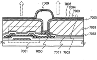
图1E示出了形成于设置有显示装置的电路的基板之上的多个晶体管的截面结构的实例。图1E所示的晶体管440A和440B各自具有一种四端子结构,在该四端子结构中有设置于关于氧化物半导体层的沟道形成区彼此相对的两侧上的,各自具有绝缘膜布置于它们之间的一对电极层。注意,其中有设置于关于氧化物半导体层的沟道形成区彼此相对的两侧上的,各自具有绝缘膜布置于它们之间的一对电极层的所谓的双栅极晶体管是本实施例的四端子结构的一种实施例。此外,还将描述其中晶体管440B被应用于显示装置的像素以及晶体管440A被应用于布置于像素部分的外围的驱动电路的一部分的情形。FIG. 1E shows an example of a cross-sectional structure of a plurality of transistors formed over a substrate provided with a circuit of a display device. The
晶体管440A包括在具有绝缘表面的基板400之上的第一电极层421a、第一绝缘层402、包括结晶区405a的氧化物半导体层404a、第二电极层455a及第三电极层455b。另外,晶体管440A包括与结晶区405a接触的并且覆盖晶体管440A的第二绝缘层428,以及设置于沟道形成区之上的第四电极层422a,第二绝缘层428置于它们之间。第一电极层421a与包括结晶区405a的氧化物半导体层404a彼此重叠,第一绝缘层402置于它们之间。此外,第二电极层455a和第三电极层455b被形成于氧化物半导体层404a之上,使得第二电极层455a的一部分、第三电极层455b的一部分与氧化物半导体层404a重叠。The
晶体管440B包括在具有绝缘表面的基板400之上的第一电极层421b、第一绝缘层402、包括结晶区405b的氧化物半导体层404b、第二电极层455c及第三电极层455d。另外,晶体管440B包括与结晶区405b接触的并且覆盖晶体管440B的第二绝缘层428,以及设置于沟道形成区之上的第四电极层422b,第二绝缘层428置于它们之间。第一电极层421b与包括结晶区405b的氧化物半导体层404b彼此重叠,第一绝缘层402置于它们之间。此外,第二电极层455c和第三电极层455d被形成于氧化物半导体层404b之上,使得第二电极层455c的一部分、第三电极层455d的一部分与氧化物半导体层404b重叠。The
晶体管440A和440B各自具有双栅极结构。在具有双栅极结构的晶体管中,设置于关于氧化物半导体层彼此相对的两侧上的电极层(各自具有绝缘膜布置于它们之间)之一或两者能够被用作栅电极层。注意,第二电极层和第三电极层起着源电极层和漏电极层的作用。
在本实施例中,晶体管440A的第四电极层422a被用作晶体管的主栅电极。因此,沟道被形成于定位于与氧化物半导体层404a的第二电极层455a接触的区域和与氧化物半导体层404a的第三电极层455b接触的区域之间的区域内,该沟道与第二绝缘层428接触并且与第四电极层422a重叠。In this embodiment, the
第一电极层和第四电极层被设置于关于氧化物半导体层的彼此相对的两侧上,各自具有绝缘膜布置于它们之间。注意,在本实施例中,在第一电极层的电位比第四电极层的电位高的情况下,第一电极层被称为主栅电极,而在第四电极层的电位比第一电极层的电位高的情况下,第四电极层被称为主栅电极。第一电极层或第四电极层的电位可以是GND、0V,或者处于浮置状态。The first electrode layer and the fourth electrode layer are provided on both sides opposite to each other with respect to the oxide semiconductor layer, each having an insulating film disposed therebetween. Note that in this embodiment, in the case where the potential of the first electrode layer is higher than that of the fourth electrode layer, the first electrode layer is referred to as a main gate electrode, and in the case where the potential of the fourth electrode layer is higher than that of the first electrode layer When the electric potential of the layer is high, the fourth electrode layer is called a main gate electrode. The potential of the first electrode layer or the fourth electrode layer may be GND, 0V, or be in a floating state.
晶体管440B的第一电极层421b被用作晶体管的主栅电极。因此,沟道被形成于定位于与氧化物半导体层404b的第二电极层455c接触的区域和与氧化物半导体层404b的第三电极层455d接触的区域之间的区域内,该沟道与第一绝缘层402接触并且与第一电极层421b重叠。The
注意,当第一电极层421b、第二电极层455c、第三电极层455b及第四电极层422b使用透光性导电膜形成时,晶体管440B能够具有透光性质。在将透光性晶体管应用于显示装置的像素的情况下,能够提高像素的开口率。Note that when the
作为透光性导电膜的材料,能够采用透射可见光的导电材料,例如,In-Sn-O基氧化物导电材料、In-Sn-Zn-O基氧化物导电材料、In-Al-Zn-O基氧化物导电材料、Sn-Ga-Zn-O基氧化物导电材料、Al-Ga-Zn-O基氧化物导电材料、Sn-Al-Zn-O基氧化物导电材料、In-Zn-O基氧化物导电材料、Sn-Zn-O基氧化物导电材料、Al-Zn-O基氧化物导电材料、In-O基氧化物导电材料、Sn-O基氧化物导电材料或Zn-O基氧化物导电材料。在使用溅射法的情况下,沉积可以用含有重量百分比大于或等于2%且小于或等于10%的SiO2的靶子来执行,使得透光性导电膜可以包含SiOx(X>0)并且是非晶的。As the material of the light-transmitting conductive film, conductive materials that transmit visible light can be used, for example, In-Sn-O-based oxide conductive materials, In-Sn-Zn-O-based oxide conductive materials, In-Al-Zn-O Based oxide conductive material, Sn-Ga-Zn-O based oxide conductive material, Al-Ga-Zn-O based oxide conductive material, Sn-Al-Zn-O based oxide conductive material, In-Zn-O Based oxide conductive material, Sn-Zn-O based oxide conductive material, Al-Zn-O based oxide conductive material, In-O based oxide conductive material, Sn-O based oxide conductive material or Zn-O based oxide conductive material. In the case of using the sputtering method, the deposition can be performed with a target containing SiO 2 in a weight percentage greater than or equal to 2% and less than or equal to 10%, so that the light-transmitting conductive film can contain SiO x (X>0) and is amorphous.
晶体管440A的第一电极层421a、第二电极层455a、第三电极层455b及第四电极层422a可以使用包括含有选自Ti、Mo、W、Al、Cr、Cu及Ta的元素作为主要成分的膜的单层结构或叠层结构来形成。对于与氧化物半导体层电连接的第二电极层455a和第三电极层455b,优选使用包含氧亲和力高的金属的材料。The
作为氧化物半导体层,能够使用为四组分金属氧化物的In-Sn-Ga-Zn-O基氧化物半导体层;为三组分金属氧化物的In-Ga-Zn-O基氧化物半导体层、In-Sn-Zn-O基氧化物半导体层、In-Al-Zn-O基氧化物半导体层、Sn-Ga-Zn-O基氧化物半导体层、Al-Ga-Zn-O基氧化物半导体层或Sn-Al-Zn-O基氧化物半导体层;为双组分金属氧化物的In-Zn-O基氧化物半导体层、Sn-Zn-O基氧化物半导体层、Al-Zn-O基氧化物半导体层、Zn-Mg-O基氧化物半导体层、Sn-Mg-O基氧化物半导体层或In-Mg-O基氧化物半导体层;或者为单组分金属氧化物的In-O基氧化物半导体层、Sn-O基氧化物半导体层或Zn-O基氧化物半导体层。此外,在上述氧化物半导体层中还可以含有SiO2。As the oxide semiconductor layer, an In-Sn-Ga-Zn-O-based oxide semiconductor layer that is a four-component metal oxide; an In-Ga-Zn-O-based oxide semiconductor that is a three-component metal oxide can be used layer, In-Sn-Zn-O-based oxide semiconductor layer, In-Al-Zn-O-based oxide semiconductor layer, Sn-Ga-Zn-O-based oxide semiconductor layer, Al-Ga-Zn-O-based oxide semiconductor layer, In-Zn-O-based oxide semiconductor layer, Sn-Zn-O-based oxide semiconductor layer, Al-Zn -O-based oxide semiconductor layer, Zn-Mg-O-based oxide semiconductor layer, Sn-Mg-O-based oxide semiconductor layer, or In-Mg-O-based oxide semiconductor layer; or a single-component metal oxide An In-O-based oxide semiconductor layer, a Sn-O-based oxide semiconductor layer, or a Zn-O-based oxide semiconductor layer. In addition, SiO 2 may be contained in the above-mentioned oxide semiconductor layer.
作为氧化物半导体层,能够使用以InMO3(ZnO)m(m>0)表示的薄膜。在此,M代表选自Ga、Al、Mn及Co的一种或多种金属元素。例如,M可以是Ga、Ga和Al、Ga和Mn、Ga和Co等。其组成公式以InMO3(ZnO)m(m>0)表示的包含Ga作为M的氧化物半导体层被称为以上所述的In-Ga-Zn-O基氧化物半导体,并且In-Ga-Zn-O氧化物半导体的薄膜被称为In-Ga-Zn-O基膜。As the oxide semiconductor layer, a thin film represented by InMO 3 (ZnO) m (m>0) can be used. Here, M represents one or more metal elements selected from Ga, Al, Mn and Co. For example, M may be Ga, Ga and Al, Ga and Mn, Ga and Co, or the like. An oxide semiconductor layer containing Ga as M whose composition formula is represented by InMO 3 (ZnO) m (m>0) is called the In-Ga-Zn-O-based oxide semiconductor described above, and In-Ga- A thin film of Zn-O oxide semiconductor is called an In-Ga-Zn-O based film.
对于氧化物半导体层,使用经受过以快速热退火(RTA)法等在短时间内于在高温下进行的脱水或脱氢的那种氧化物半导体层。该加热过程使得氧化物半导体层的浅表部分具有包含具有大于或等于1nm且小于或等于20nm的晶粒尺寸的所谓的纳米晶体的结晶区,并且氧化物半导体层的剩余部分是非晶的或者由非晶和微晶的混合物形成,其中非晶区散布有微晶体。注意,纳米晶体的上述尺寸只是一个示例,本发明并不应被理解为仅限于以上范围。For the oxide semiconductor layer, one subjected to dehydration or dehydrogenation at a high temperature in a short time by a rapid thermal annealing (RTA) method or the like is used. This heating process causes the superficial portion of the oxide semiconductor layer to have a crystalline region containing so-called nanocrystals having a grain size of 1 nm or more and 20 nm or less, and the remaining portion of the oxide semiconductor layer is amorphous or made of A mixture of amorphous and microcrystalline forms, with amorphous regions interspersed with microcrystals. Note that the above-mentioned size of the nanocrystal is just an example, and the present invention should not be construed as being limited to the above-mentioned range.
在具有该结构的氧化物半导体层中,包含纳米晶体的致密的结晶区存在于其浅表部分。因此,在使用这样的氧化物半导体层的情况下,能够防止转变为n型,该转变被归因于湿气进入浅表部分或者氧自浅表部分中消除。结果,能够防止由转变为n型所影响的电特性的劣化,尤其是断态电流的增加。In the oxide semiconductor layer having this structure, a dense crystalline region containing nanocrystals exists in its superficial portion. Therefore, in the case of using such an oxide semiconductor layer, it is possible to prevent transition to n-type, which is attributed to entry of moisture into the shallow portion or elimination of oxygen from the shallow portion. As a result, deterioration of electrical characteristics affected by transition to n-type, especially increase in off-state current can be prevented.
在氧化物半导体层的浅表部分的结晶区包括其中c轴沿着基本上垂直于氧化物半导体层的表面的方向来取向的晶粒。例如,在使用In-Ga-Zn-O基氧化物半导体材料的情况下,在结晶区内的In2Ga2ZnO7晶粒的c轴沿着基本上垂直于氧化物半导体层的表面的方向来取向。结晶区包括沿着预定方向来取向的纳米晶体。例如,在In-Ga-Zn-O基氧化物半导体材料被用于氧化物半导体层并且纳米晶体被排列使得In2Ga2ZnO7的c轴沿着基本上垂直于基板平面(或氧化物半导体层的表面)的方向来取向的情况下,电流沿着晶体管内的In2Ga2ZnO7的b轴方向(或a轴方向)流动。The crystalline region in the shallow portion of the oxide semiconductor layer includes crystal grains in which the c-axis is oriented in a direction substantially perpendicular to the surface of the oxide semiconductor layer. For example, in the case of using an In-Ga-Zn-O-based oxide semiconductor material, the c-axis of the In 2 Ga 2 ZnO 7 grains in the crystalline region is along a direction substantially perpendicular to the surface of the oxide semiconductor layer to orientation. The crystalline region includes nanocrystals oriented along a predetermined direction. For example, where an In-Ga-Zn-O-based oxide semiconductor material is used for the oxide semiconductor layer and the nanocrystals are arranged such that the c-axis of In 2 Ga 2 ZnO 7 is along a plane substantially perpendicular to the substrate (or the oxide semiconductor In the case of aligning in the direction of the surface of the layer), the current flows along the b-axis direction (or a-axis direction) of In 2 Ga 2 ZnO 7 in the transistor.
注意,结晶区可以包括不同于晶粒的部分。晶粒的晶体结构并不仅限于上述结构,而是结晶区可以包括别的结构的晶粒。例如,在使用In-Ga-Zn-O基氧化物半导体材料的情况下,除了In2Ga2ZnO7的晶粒之外,还可以包括InGaZnO4的晶粒。Note that the crystalline region may include portions other than crystal grains. The crystal structure of the crystal grains is not limited to the above structures, but the crystallized region may include crystal grains of other structures. For example, in the case of using an In-Ga-Zn-O-based oxide semiconductor material, crystal grains of InGaZnO 4 may be included in addition to crystal grains of In 2 Ga 2 ZnO 7 .
以下,参照图1A到1E来描述在一个基板之上的晶体管440A和晶体管440B的制造过程。Hereinafter, a manufacturing process of the
首先,在具有绝缘表面的基板400之上形成导电膜,并且对其执行第一光刻步骤以形成第一电极层421a和第一电极层421b。此时,优选地执行蚀刻,使得至少第一电极层421a和第一电极层421b的端部锥形化以便防止断连。First, a conductive film is formed over the
注意,抗蚀剂掩模可以用喷墨法来形成。用喷墨法来形成抗蚀剂掩模不需要光掩模;因而,能够降低制造成本。不必说,不经能够将喷墨法应用于第一光刻步骤,而且还能够应用于别的光刻步骤。Note that the resist mask can be formed by an inkjet method. Forming a resist mask by an inkjet method does not require a photomask; thus, manufacturing costs can be reduced. Needless to say, the inkjet method can be applied not only to the first photolithography step but also to other photolithography steps.
注意,作为基板400,能够使用下列基板中的任一种:以熔融法或浮法使用钡硼硅酸盐玻璃、铝硼硅酸盐玻璃、铝硅酸盐玻璃等形成的非碱性玻璃基板;陶瓷基板;具有足以经受住该制造过程的处理温度的耐热性的塑料基板等。作为选择,同样可以使用金属基板,例如在表面上设置有绝缘膜的不锈钢合金基板。Note that, as the
注意,作为上述玻璃基板,可以使用由诸如陶瓷基板、石英基板或蓝宝石基板之类的绝缘体形成的基板。作为选择,可以使用结晶玻璃基板等。Note that, as the above-mentioned glass substrate, a substrate formed of an insulator such as a ceramic substrate, a quartz substrate, or a sapphire substrate can be used. Alternatively, a crystallized glass substrate or the like may be used.
第一电极层421a和第一电极层421b能够使用应用下列材料中的任一种材料的单层或叠层来形成:金属材料,例如,铝、铜、钼、钛、铬、钽、钨、钕或钪;含有这些材料中的任一种作为主要成分的合金材料;以及含有这些材料中的任一种的氮化物。优选地,有效的是利用诸如铝或铜之类的低电阻金属材料来形成第一电极层,低电阻金属材料优选地结合难熔金属材料来使用,因为它具有诸如低耐热性和低腐蚀倾向之类的优点。作为难熔金属材料,能够使用钼、钛、铬、钽、钨、钕、钪等。The
此时,透光性氧化物导电层被用于电极层和布线层的一部分以提高开口率。例如,能够将包含氧化铟、氧化铟和氧化锡的合金、氧化铟和氧化锌的合金、氧化锌、氧化锌铝、氧氮化锌铝、氧化锌镓等的氧化物导电层用于透光性导电层。At this time, a light-transmitting oxide conductive layer is used for a part of the electrode layer and the wiring layer to increase the aperture ratio. For example, an oxide conductive layer including indium oxide, an alloy of indium oxide and tin oxide, an alloy of indium oxide and zinc oxide, zinc oxide, aluminum zinc oxide, aluminum zinc oxynitride, gallium zinc oxide, etc., can be used for light transmission. conductive layer.
此外,第一电极层421a和第一电极层421b可以使用不同的材料来形成。例如,为了提高像素部分的开口率,第一电极层421b能够使用对于可见光透光的导电层形成,并且为了抑制布线电阻,在驱动电路部分中的第一电极层421a能够使用包含金属作为其主要成分的导电膜来形成,例如,含有选自钛、钼、钨、铝、铬、铜及钽的元素作为主要成分的单层膜或者包含该膜的叠层膜。In addition, the
用作基膜的绝缘层可以被设置于基板400与第一电极层421a和421b之间。基膜具有防止杂质元素从基板400内扩散出的功能,并且能够形成为具有包含氮化硅膜、氧化硅膜、氮氧化硅膜及氧氮化硅膜中的一种或多种的单层或叠层结构。An insulating layer serving as a base film may be disposed between the
然后,在第一电极层421a和第一电极层421b之上形成第一绝缘层402。作为第一绝缘层402,能够使用氧化硅层、氧氮化硅层、氮氧化硅层、氮化硅层、氧化铝层、氧化钽层等中的任一种的单层膜或叠层膜。第一绝缘层402以CVD法、溅射法等形成至大于或等于50nm且小于或等于250nm的厚度。注意,在第一绝缘层402内,氧化物绝缘层被优选地设置于第一绝缘层402与氧化物半导体层接触的那侧上。Then, the first insulating
注意,由于杂质的去除而变成i型或者变成基本上i型(纯净化的氧化物半导体)的氧化物半导体对界面状态密度或界面电荷是极其敏感的;因此,具有绝缘膜的界面是重要的。因此,与具有高纯度的氧化物半导体接触的绝缘膜需要是高质量的。Note that an oxide semiconductor that becomes i-type or substantially i-type (purified oxide semiconductor) due to removal of impurities is extremely sensitive to interface state density or interface charge; therefore, an interface with an insulating film is important. Therefore, an insulating film in contact with an oxide semiconductor having high purity needs to be of high quality.
例如,使用微波(2.45GHz)的高密度的等离子体CVD是优选的,因为它会产生具有高介质耐压的致密的高质量绝缘膜。这是因为在具有高纯度的氧化物半导体与高质量栅极绝缘膜之间的紧密接触会降低界面状态密度并且产生有利的界面特性。For example, high-density plasma CVD using microwaves (2.45 GHz) is preferable because it produces a dense high-quality insulating film with high dielectric withstand voltage. This is because close contact between an oxide semiconductor having high purity and a high-quality gate insulating film reduces interface state density and produces favorable interface characteristics.
另外,由于使用高密度的等离子体CVD设备形成的绝缘膜能够具有均匀的厚度,因而绝缘膜具有优良的台阶覆盖率。此外,以高密度的等离子体CVD设备形成的绝缘薄膜的厚度能够被精确地控制。In addition, since the insulating film formed using a high-density plasma CVD apparatus can have a uniform thickness, the insulating film has excellent step coverage. In addition, the thickness of an insulating film formed with a high-density plasma CVD apparatus can be precisely controlled.
不必说,能够采用诸如溅射法或等离子体CVD法之类的其他方法,只要该方法能够形成作为栅极绝缘膜的好质量的绝缘膜。作为选择,可以使用其膜质量以及与氧化物半导体间的界面特性通过在绝缘膜形成之后执行的热处理来提高的绝缘膜。在任何情况下,具有降低的与氧化物半导体间的界面状态密度的并且能够形成有利的界面,以及具有作为栅极绝缘膜的有利的膜质量的任意绝缘膜都能够使用。Needless to say, other methods such as a sputtering method or a plasma CVD method can be employed as long as the method can form an insulating film of good quality as a gate insulating film. Alternatively, an insulating film whose film quality and interface characteristics with an oxide semiconductor are improved by heat treatment performed after the insulating film is formed may be used. In any case, any insulating film that has a reduced interface state density with an oxide semiconductor and can form a favorable interface, and has favorable film quality as a gate insulating film can be used.
第一绝缘层402使用高密度的等离子体CVD设备来形成。在此,高密度的等离子体CVD设备指的是能够实现高于或等于1×10¹¹/cm3的等离子体密度的设备。例如,等离子体通过施加高于或等于3kW且低于或等于6kW的微波功率来生成,从而形成绝缘膜。The first insulating
甲硅烷气体(SiH4)、氧化亚氮(N2O)及稀有气体被作为源气体引入腔室之内以在高于或等于10Pa且低于或等于30Pa的压力下生成高密度的等离子体,使得绝缘膜形成于具有绝缘表面的基板(例如,玻璃基板)之上。之后,可以停止供应甲硅烷气体,并且在不暴露于空气的情况下可以引入氧化亚氮(N2O)和稀有气体以执行对绝缘膜的表面执行的等离子体处理。通过引入氧化亚氮(N2O)和稀有气体来对绝缘膜的表面执行的等离子体处理至少在绝缘膜形成之后执行。通过上述处理过程形成的绝缘膜具有小的厚度并且是其可靠性即使它具有例如小于100nm的厚度也能够得以保证的绝缘膜。Monosilane gas (SiH 4 ), nitrous oxide (N 2 O) and rare gases are introduced into the chamber as source gases to generate high-density plasma at a pressure higher than or equal to 10Pa and lower than or equal to 30Pa , so that an insulating film is formed over a substrate (for example, a glass substrate) having an insulating surface. After that, the supply of monosilane gas may be stopped, and nitrous oxide (N 2 O) and a rare gas may be introduced to perform plasma treatment performed on the surface of the insulating film without exposure to air. The plasma treatment performed on the surface of the insulating film by introducing nitrous oxide (N 2 O) and a rare gas is performed at least after the insulating film is formed. The insulating film formed through the above-described process has a small thickness and is an insulating film whose reliability can be ensured even if it has a thickness of, for example, less than 100 nm.
在形成第一绝缘层402时,被引入腔室之内的甲硅烷气体(SiH4)对氧化亚氮(N2O)的流量比为1:10到1:200。另外,作为被引入腔室内的稀有气体,能够使用氦气、氩气、氪气、氙气等。特别地,优选地使用廉价的氩气。When forming the first insulating
另外,由于使用高密度的等离子体设备形成的绝缘膜能够具有均匀的厚度,因而绝缘膜具有优良的台阶覆盖率。此外,以高密度的等离子体设备,能够精确地控制绝缘薄膜的厚度。In addition, since the insulating film formed using a high-density plasma device can have a uniform thickness, the insulating film has excellent step coverage. In addition, with high-density plasma equipment, the thickness of the insulating film can be precisely controlled.
通过上述处理过程形成的绝缘膜与使用常规的平行板式PCVD设备形成的绝缘膜大为不同。在以相同的蚀刻剂进行的蚀刻的速率相互比较的情况下,通过上述处理过程形成的绝缘膜的时刻速率比使用常规的平行板式PCVD设备形成的绝缘膜的蚀刻速率低大于或等于10%或者大于或等于20%。因而,可以说,使用高密度的等离子体设备形成的绝缘膜是致密的膜。The insulating film formed by the above-described process is greatly different from that formed using a conventional parallel-plate type PCVD apparatus. In the case where the etching rates performed with the same etchant are compared with each other, the moment rate of the insulating film formed by the above process is lower than the etching rate of the insulating film formed using a conventional parallel plate type PCVD apparatus by 10% or more or greater than or equal to 20%. Therefore, it can be said that an insulating film formed using a high-density plasma device is a dense film.
作为选择,以CVD法使用有机硅烷气体形成的氧化硅层能够用于第一绝缘层402。作为有机硅烷气体,能够使用含硅的化合物,例如,正硅酸乙酯(TEOS)(化学式:Si(OC2H5)4)、四甲基硅烷(TMS)(化学式:Si(CH3)4)、四甲基环四硅氧烷(TMCTS)、八甲基环四硅氧烷(OMCTS)、六甲基二硅氮烷(HMDS)、三乙氧基硅烷(化学式:SiH(OC2H5)3)或三(二甲胺基)硅烷(化学式:SiH(N(CH3)2)3)。Alternatively, a silicon oxide layer formed by a CVD method using organosilane gas can be used for the first insulating
作为选择,第一绝缘层402可以使用铝、钇或铪的氧化物、氮化物、氧氮化物及氮氧化物中的一种或者包含上述材料中的至少两种或更多种的化合物来形成。Alternatively, the first insulating
注意,在本说明书中,氧氮化物指的是含有比氮原子多的氧原子的物质,而氮氧化物指的是含有比氧原子多的氮原子的物质。例如,“氧氮化硅膜”意指这样的膜:含有氧原子和氮原子使得氧原子的数量大于氮原子的数量,并且在使用卢瑟福被散射光谱法(RBS)和氢前向散射(HFS)来执行测量的情况下,含有原子百分比浓度分别为50%~70%、0.5%~15%、25%~35%及0.1%~10%的氧、氮、硅及氢。此外,“氮氧化硅膜”意指这样的膜:含有氮原子和氧原子使得氮原子的数量大于氧原子的数量,并且在使用RBS和HFS来执行测量的情况下,含有原子百分比浓度分别为5%~30%、20%~55%、25%~35%及10%~30%的氧、氮、硅及氢。注意,当在氧氮化硅膜或氮氧化硅膜内所含的原子的总数被定义为100%(原子百分比)时,氮、氧、硅及氢的百分比落在以上给定的范围之内。Note that in this specification, oxynitride refers to a substance containing more oxygen atoms than nitrogen atoms, and nitrogen oxide refers to a substance containing more nitrogen atoms than oxygen atoms. For example, "silicon oxynitride film" means a film that contains oxygen atoms and nitrogen atoms such that the number of oxygen atoms is greater than the number of nitrogen atoms, and the (HFS) to perform the measurement, containing oxygen, nitrogen, silicon and hydrogen at atomic percent concentrations of 50%~70%, 0.5%~15%, 25%~35%, and 0.1%~10%, respectively. Furthermore, "silicon oxynitride film" means a film containing nitrogen atoms and oxygen atoms such that the number of nitrogen atoms is greater than that of oxygen atoms, and in the case of performing measurement using RBS and HFS, containing atomic percent concentrations of 5%~30%, 20%~55%, 25%~35% and 10%~30% of oxygen, nitrogen, silicon and hydrogen. Note that when the total number of atoms contained in a silicon oxynitride film or a silicon oxynitride film is defined as 100% (atomic percent), the percentages of nitrogen, oxygen, silicon, and hydrogen fall within the ranges given above .
然后,在第一绝缘层402之上,氧化物半导体膜403被形成达大于或等于5nm且小于或等于200nm的,优选地大于或等于10nm且小于或等于20nm的厚度(参见图1A)。Then, over the first insulating
注意,在氧化物半导体膜403形成之前,在第一绝缘层402的表面上的灰尘优选地通过反溅射来去除,在该反溅射中氩气被引入并且生成等离子体。反溅射指的是这样的方法:在不对靶子一侧施加电压的情况下,RF电源被用于在氩气气氛中对基板一侧施加电压,以在基板附近生成等离子体,从而使表面改性。注意,代替氩气气氛,可以使用氮气气氛、氦气气氛等。作为选择,可以使用其中添加了氧气、N2O等的氩气气氛。此外,作为选择,可以使用其中添加了Cl2、CF4等的氩气气氛。在反溅射之后,氧化物半导体膜在不暴露于空气的情况下形成,由此能够防止灰尘或湿气贴附于第一绝缘层402与氧化物半导体膜403之间的界面。Note that before the
作为氧化物半导体膜,能够使用作为以上所述的四组分金属氧化物的In-Sn-Ga-Zn-O基氧化物半导体层;作为以上所述的三组分金属氧化物的In-Ga-Zn-O基氧化物半导体层、In-Sn-Zn-O基氧化物半导体层、In-Al-Zn-O基氧化物半导体层、Sn-Ga-Zn-O基氧化物半导体层、Al-Ga-Zn-O基氧化物半导体层或Sn-Al-Zn-O基氧化物半导体层;作为以上所述的双组分金属氧化物的In-Zn-O基氧化物半导体层、Sn-Zn-O基氧化物半导体层、Al-Zn-O基氧化物半导体层、Zn-Mg-O基氧化物半导体层、Sn-Mg-O基氧化物半导体层或In-Mg-O基氧化物半导体层;或者作为以上所述的单组分金属氧化物的In-O基氧化物半导体层、Sn-O基氧化物半导体层或Zn-O基氧化物半导体层。此外,在上述氧化物半导体膜中可以含有SiO2。作为氧化物半导体膜,能够使用上述以InMO3(ZnO)m(m>0)表示的薄膜。As the oxide semiconductor film, an In-Sn-Ga-Zn-O-based oxide semiconductor layer that is the above-mentioned four-component metal oxide; an In-Ga that is the above-mentioned three-component metal oxide can be used; -Zn-O-based oxide semiconductor layer, In-Sn-Zn-O-based oxide semiconductor layer, In-Al-Zn-O-based oxide semiconductor layer, Sn-Ga-Zn-O-based oxide semiconductor layer, Al - a Ga-Zn-O-based oxide semiconductor layer or a Sn-Al-Zn-O-based oxide semiconductor layer; an In-Zn-O-based oxide semiconductor layer as the above-mentioned two-component metal oxide, a Sn- Zn-O-based oxide semiconductor layer, Al-Zn-O-based oxide semiconductor layer, Zn-Mg-O-based oxide semiconductor layer, Sn-Mg-O-based oxide semiconductor layer, or In-Mg-O-based oxide semiconductor layer a semiconductor layer; or an In-O-based oxide semiconductor layer, a Sn-O-based oxide semiconductor layer, or a Zn-O-based oxide semiconductor layer which is the above-mentioned one-component metal oxide. In addition, SiO 2 may be contained in the above-mentioned oxide semiconductor film. As the oxide semiconductor film, the above-mentioned thin film represented by InMO 3 (ZnO) m (m>0) can be used.
氧化物半导体膜能够以溅射法在稀有气体(典型为氩气)气氛、氧气气氛或者稀有气体(典型为氩气)和氧气的气氛中形成。在使用溅射法的情况下,膜沉积可以使用含有重量百分比大于或等于2%且小于或等于10%的SiO2的靶子来执行,并且在氧化物半导体膜中可以含有抑制晶化的SiOx(x>0)。The oxide semiconductor film can be formed in a rare gas (typically argon) atmosphere, an oxygen atmosphere, or a rare gas (typically argon) and oxygen atmosphere by a sputtering method. In the case of using the sputtering method, film deposition can be performed using a target containing SiO 2 in a weight percentage of 2% or more and 10% or less, and SiOx ( x>0).
在此,膜形成在下列条件下使用用于形成包含In、Ga及Zn的氧化物半导体(组成比为In2O3:Ga2O3:ZnO=1:1:1[摩尔比]或者In2O3:Ga2O3:ZnO=1:1:2[摩尔比])的靶子来执行:在基板与靶子之间的距离为100mm,压力为0.6Pa,直流(DC)电源为0.5kW,以及气氛为氧气(氧气的流量为100%)。注意,脉冲直流(DC)电源是优选的,因为在膜形成时所生成的粉状物质(也称为粒子或灰尘)能够被减少并且膜的厚度分布能够是均匀的。在本实施例中,作为氧化物半导体膜,具有15nm的厚度的In-Ga-Zn-O基膜以溅射法使用用于形成In-Ga-Zn-O基氧化物半导体的靶子来形成。Here, the film formation was used under the following conditions for forming an oxide semiconductor containing In, Ga, and Zn (composition ratio: In 2 O 3 :Ga 2 O 3 :ZnO=1:1:1 [molar ratio] or In 2 O 3 :Ga 2 O 3 :ZnO=1:1:2[molar ratio]) target: the distance between the substrate and the target is 100mm, the pressure is 0.6Pa, and the direct current (DC) power supply is 0.5kW , and the atmosphere is oxygen (the flow of oxygen is 100%). Note that a pulsed direct current (DC) power supply is preferable because powdery substances (also referred to as particles or dust) generated at the time of film formation can be reduced and the thickness distribution of the film can be uniform. In this embodiment, as the oxide semiconductor film, an In-Ga-Zn-O-based film having a thickness of 15 nm was formed by a sputtering method using a target for forming an In-Ga-Zn-O-based oxide semiconductor.
在这种情况下,氧化物半导体膜优选地在保留于处理腔室内的湿气被去除的同时形成。这是为了防止在氧化物半导体膜内含有氢、羟基或湿气。In this case, the oxide semiconductor film is preferably formed while moisture remaining in the processing chamber is removed. This is to prevent hydrogen, hydroxyl groups, or moisture from being contained in the oxide semiconductor film.
另外,优选的是,氧化物半导体膜被连续地形成于第一绝缘层402之上。在此所使用的多腔室溅射设备设置有硅或氧化硅(人造石英)的靶子,以及用于形成氧化物半导体膜的靶子。设置有用于形成氧化物半导体膜的靶子的沉积腔室还至少设置有低温泵作为排空单元。注意,可以使用涡轮分子泵来代替低温泵,并且可以在涡轮分子泵的进气口上方设置冷阱使得湿气等可以被吸收。In addition, it is preferable that the oxide semiconductor film is formed continuously over the first insulating
从以低温泵排空的沉积腔室中,氢原子、含有氢原子的化合物(例如,H2O)、碳原子、含有碳原子的化合物等被去除,由此能够降低在形成于沉积腔室中的氧化物半导体膜内的杂质的浓度。From the deposition chamber evacuated by the cryopump, hydrogen atoms, compounds containing hydrogen atoms (for example, H 2 O), carbon atoms, compounds containing carbon atoms, etc. concentration of impurities in the oxide semiconductor film.
优选的是,其中诸如氢、水、羟基或氢化物之类的杂质被降低至近似ppm级或ppb级的高纯度气体被用作用于沉积氧化物半导体膜的溅射气体。It is preferable that a high-purity gas in which impurities such as hydrogen, water, hydroxyl groups, or hydrides are reduced to approximately the ppm level or the ppb level is used as the sputtering gas for depositing the oxide semiconductor film.
氧化物半导体膜可以在基板被加热的状态下形成。在那时,基板被加热到高于或等于100°C且低于或等于600°C,优选地,高于或等于200°C且低于或等于400°C。通过在沉积期间加热基板,能够降低在氧化物半导体膜内的杂质浓度。The oxide semiconductor film can be formed while the substrate is heated. At that time, the substrate is heated to a temperature higher than or equal to 100°C and lower than or equal to 600°C, preferably, higher than or equal to 200°C and lower than or equal to 400°C. By heating the substrate during deposition, the impurity concentration within the oxide semiconductor film can be reduced.
溅射法的实例包括其中高频电源被用作溅射电源的RF溅射法、其中直流电源被使用的DC溅射法,以及其中偏压以脉冲的方式来施加的脉冲DC溅射法。RF溅射法主要是在形成绝缘膜的情况下使用,而DC溅射法主要是在形成金属导电膜的情况下使用。Examples of the sputtering method include an RF sputtering method in which a high-frequency power source is used as a sputtering power source, a DC sputtering method in which a direct current power source is used, and a pulsed DC sputtering method in which a bias voltage is applied in a pulsed manner. The RF sputtering method is mainly used when forming an insulating film, and the DC sputtering method is mainly used when forming a metal conductive film.
另外,还有其中能够设置不同材料的多个靶子的多源溅射设备。以多源溅射设备,不同材料的膜能够被形成为在同一腔室内堆叠,或者多种材料的膜能够通过在同一腔室内同时放电来形成。In addition, there is also a multi-source sputtering apparatus in which a plurality of targets of different materials can be set. With a multi-source sputtering apparatus, films of different materials can be formed to be stacked in the same chamber, or films of multiple materials can be formed by simultaneously discharging in the same chamber.
另外,还有在腔室内设置有磁体系统并且用于磁控溅射的溅射设备,以及用于其中利用微波来生成的等离子体在不使用辉光放电的情况下使用的ECR溅射的溅射设备。In addition, there are sputtering equipment provided with a magnet system inside a chamber and used for magnetron sputtering, and sputtering equipment used for ECR sputtering in which plasma generated by microwaves is used without using glow discharge. shooting equipment.
而且,作为借助于溅射的沉积方法,还有其中靶子物质和溅射气体组分在沉积期间彼此发生化学反应以形成它们的化合物薄膜的反应溅射法,以及其中在沉积期间同样对基板施加电压的偏压溅射法。Furthermore, as a deposition method by sputtering, there is also a reactive sputtering method in which a target substance and sputtering gas components chemically react with each other during deposition to form their compound thin films, and in which a substrate is also applied to a substrate during deposition. Voltage bias sputtering method.
然后,通过第二光刻步骤,形成抗蚀剂掩模。然后,蚀刻In-Ga-Zn-O基膜。在蚀刻中,能够将诸如柠檬酸或草酸之类的有机酸用作蚀刻剂。该蚀刻被执行,使得氧化物半导体层404a和404b的端部具有锥形形状,从而能够防止因台阶形状所致的布线的破损。注意,蚀刻在此并不仅限于湿法蚀刻,而是同样可以使用干法蚀刻。Then, by a second photolithography step, a resist mask is formed. Then, the In-Ga-Zn-O base film is etched. In etching, an organic acid such as citric acid or oxalic acid can be used as an etchant. This etching is performed so that the end portions of the
然后,执行氧化物半导体层404a和404b的脱水或脱氢。用于脱水或脱氢的第一热处理能够利用电阻加热法、灯照射等在惰性气体气氛中通过快速热退火(RTA)处理在高于或等于500°C且低于或等于750°C的温度(或者低于或等于玻璃基板的应变点的温度)下执行大约1分钟到10分钟,优选地在650°C下执行大约大于或等于3分钟且小于或等于6分钟。以RTA法,脱水或脱氢能够短时间地执行;因此,处理甚至能够在高于玻璃基板的应变点的温度下执行。注意,热处理的时序并不仅限于该时序,而是可以多次执行,例如,在光刻步骤或沉积步骤之前及之后。Then, dehydration or dehydrogenation of the
注意,在本说明书中,在惰性气体(例如,氮气或稀有气体)气氛内的热处理被称为用于脱水或脱氢的热处理。在本说明书中,脱氢并不只是指通过热处理进行的形式为H2的消除,而且为了方便起见,脱水或脱氢还指的是H、OH等的消除。Note that, in this specification, heat treatment in an inert gas (for example, nitrogen or rare gas) atmosphere is referred to as heat treatment for dehydration or dehydrogenation. In this specification, dehydrogenation does not mean only elimination in the form of H2 by heat treatment, but dehydration or dehydrogenation also means elimination of H, OH, etc. for convenience.
重要的是,温度在用于脱水或脱氢的同一炉子内从在其下使氧化物半导体层脱水或脱氢的加热温度T降低到室温,防止氧化物半导体层暴露于空气,从而防止水或氢进入氧化物半导体层之内。当晶体管使用i型氧化物半导体层来形成时,该i型氧化物半导体层通过经由脱水或脱氢而使氧化物半导体层变成处于缺氧状态的低电阻氧化物半导体层,即,n型(例如,n-型或n+型)氧化物半导体层,以及通过经由氧供应而使低电阻氧化物半导体层变成高电阻氧化物半导体层来获得,晶体管的阈值电压能够是正的,从而能够实现具有所谓的常关(normally-off)特性的开关元件。优选的是,在显示装置的晶体管中的沟道被形成为处于尽可能接近于0V的正阈值电压。如果晶体管的阈值电压是负的,则它倾向于是常开的(normally on);换言之,即使在栅极电压为0V时也有电流在源电极与漏电极之间流过。在有源矩阵显示装置中,包含于电路内的晶体管的电特性是重要的,并且显示装置的性能取决于电特性。特别地,在晶体管的电特性中,阈值电压(Vth)是重要的。当阈值电压值为高或者为负值时,即使在场效应迁移率为高时,也难以控制电路。在晶体管具有高阈值电压的情况下,该晶体管不能执行作为晶体管的开关功能,并且在晶体管以低电压驱动时可能是负载。在n沟道晶体管的情形中,所期望的是,仅在正电压被施加作为栅极电压之后,才形成沟道并且有漏极电流流过。其中沟道只有在驱动电压被提高时才形成的晶体管以及其中即使在施加负电压时也会形成沟道并且有漏极电流流过的晶体管不适用于电路内所使用的晶体管。It is important that the temperature is lowered from the heating temperature T under which the oxide semiconductor layer is dehydrated or dehydrogenated to room temperature in the same furnace used for dehydration or dehydrogenation, preventing the oxide semiconductor layer from being exposed to air, thereby preventing water or Hydrogen enters into the oxide semiconductor layer. When a transistor is formed using an i-type oxide semiconductor layer, the i-type oxide semiconductor layer becomes a low-resistance oxide semiconductor layer in an oxygen-deficient state by dehydration or dehydrogenation, that is, an n-type oxide semiconductor layer. (for example, n - type or n + -type) oxide semiconductor layer, and obtained by changing the low-resistance oxide semiconductor layer to a high-resistance oxide semiconductor layer through oxygen supply, the threshold voltage of the transistor can be positive, thereby enabling A switching element having a so-called normally-off characteristic is realized. It is preferred that the channels in the transistors of the display device be formed at a positive threshold voltage as close to 0V as possible. If the threshold voltage of a transistor is negative, it tends to be normally on; in other words, a current flows between the source and drain electrodes even when the gate voltage is 0V. In an active matrix display device, the electrical characteristics of transistors included in a circuit are important, and the performance of the display device depends on the electrical characteristics. In particular, the threshold voltage (V th ) is important in the electrical characteristics of a transistor. When the threshold voltage value is high or negative, it is difficult to control the circuit even when the field effect mobility is high. In the case where a transistor has a high threshold voltage, the transistor cannot perform a switching function as a transistor, and may be a load when the transistor is driven at a low voltage. In the case of an n-channel transistor, it is desirable that only after a positive voltage is applied as a gate voltage, a channel is formed and a drain current flows. A transistor in which a channel is formed only when a driving voltage is raised and a transistor in which a channel is formed even when a negative voltage is applied and a drain current flows are not suitable for transistors used in circuits.
另外,当温度从加热温度T开始降低时,气体气氛可以切换为与在温度被升高至加热温度T时所使用的气体气氛不同的气体气氛。例如,冷却通过使用用于脱水或脱氢的同一炉子以及通过以高纯度的氧气、高纯度的N2O气体或超干燥空气(具有-40°C或更低的,优选为-60°C或更低的露点)充满炉子来执行,不暴露于空气。In addition, when the temperature is lowered from the heating temperature T, the gas atmosphere may be switched to a gas atmosphere different from the gas atmosphere used when the temperature is raised to the heating temperature T. For example, cooling is achieved by using the same furnace used for dehydration or dehydrogenation and by heating with high-purity oxygen, high-purity N2O gas or ultra-dry air (with a temperature of -40°C or lower, preferably -60°C or lower dew point) to perform with a full furnace, not exposed to air.
注意,在第一热处理中,优选的是,在气氛中不含有水、氢等。作为选择,被引入热处理设备之内的惰性气体的纯度优选地为6N(99.9999%)或更高,更优选地为7N(99.99999%)或更高(也就是,杂质浓度为1ppm或更低,优选地为0.1ppm或更低)。Note that in the first heat treatment, it is preferable not to contain water, hydrogen, or the like in the atmosphere. Alternatively, the purity of the inert gas introduced into the heat treatment apparatus is preferably 6N (99.9999%) or higher, more preferably 7N (99.99999%) or higher (that is, the impurity concentration is 1 ppm or lower, preferably 0.1 ppm or less).
在热处理于惰性气体气氛下执行的情形中,氧化物半导体层通过热处理改变成缺氧型氧化物半导体层,以成为低电阻氧化物半导体层,即n型(例如,n–型)氧化物半导体层。之后,通过形成与氧化物半导体层接触的氧化物绝缘层来给该氧化物半导体层的缺氧部分供应氧。因而,使得氧化物半导体层成为i型;也就是,氧化物半导体层被改变成高电阻氧化物半导体层。因此,有可能形成具有有利的电特性的高可靠性的晶体管。In the case where the heat treatment is performed under an inert gas atmosphere, the oxide semiconductor layer is changed into an oxygen-deficient type oxide semiconductor layer by the heat treatment to become a low-resistance oxide semiconductor layer, that is, an n-type (for example, n - type) oxide semiconductor layer. After that, oxygen is supplied to the oxygen-deficient portion of the oxide semiconductor layer by forming an oxide insulating layer in contact with the oxide semiconductor layer. Thus, the oxide semiconductor layer is made i-type; that is, the oxide semiconductor layer is changed into a high-resistance oxide semiconductor layer. Therefore, it is possible to form a highly reliable transistor with favorable electrical characteristics.
在于上述条件下充分脱水或脱氢的氧化物半导体层中,即使在脱水或脱氢的氧化物半导体层的温度增加至450°C时,显示有湿气排出的两个频谱峰值中的至少在高于或等于250°C且低于或等于300°C附近的峰值由热脱附谱法(TDS)检测到。In the oxide semiconductor layer sufficiently dehydrated or dehydrogenated under the above conditions, even when the temperature of the dehydrated or dehydrogenated oxide semiconductor layer is increased to 450° C., at least one of the two spectral peaks showing moisture discharge is Peaks around 250°C above or equal to 300°C below or equal to were detected by thermal desorption spectroscopy (TDS).
注意,在氧化物半导体层404a和404b处于原始沉积(as-depo)状态的阶段,氧化物半导体层404a和氧化物半导体层404b每个都是具有许多悬挂键的非晶层。通过用于脱水或脱氢的第一加热步骤,相互紧靠而存在的悬挂键被键合,使得氧化物半导体层404a和404b能够具有有序的非晶结构。在进行排序时,氧化物半导体层404a和404b由非晶和微晶的混合物形成,其中非晶区散布有微晶体,或者由非晶形成。包含纳米晶体的结晶区405a和结晶区405b被形成于氧化物半导体层404a和氧化物半导体层404b的浅表部分(图1B)。氧化物半导体层404a和氧化物半导体层404b的剩余部分变成为非晶的或者由非晶和微晶的混合物形成,其中非晶区散布有微晶体。注意,结晶区405a和结晶区405b分别是氧化物半导体层404a和氧化物半导体层404b的一部分,并且在下文中,“氧化物半导体层404a”和“氧化物半导体层404b”分别包括结晶区405a和结晶区405b。在此,微晶体是具有大于或等于1nm且小于或等于20nm的粒子尺寸的所谓的纳米晶体,该尺寸小于通常称为微晶体的微晶粒子的尺寸。Note that at the stage where the
在结晶区405a和405b中,优选地形成c轴沿垂直于层的表面的方向取向的纳米晶体。在这种情况下,优选的是,晶体管的长轴沿着c轴方向,而沿短轴方向的尺寸大于或等于1nm且小于或等于20nm。In the
注意,结晶区没有形成于氧化物半导体层的侧表面部分,这取决于步骤的顺序,并且在这种情况下,结晶区仅形成于浅表部分,不形成于侧表面部分。但是,侧表面部分的面积是小的,并且在这种情况下同样能够保持抑制电特性劣化或提高介质耐压的效果。Note that the crystallized region is not formed at the side surface portion of the oxide semiconductor layer, depending on the order of steps, and in this case, the crystallized region is formed only at the superficial portion, not at the side surface portion. However, the area of the side surface portion is small, and the effects of suppressing deterioration of electrical characteristics or improving dielectric withstand voltage can also be maintained in this case.
此外,第一电极层421a和第一电极层421b被晶化以在某些情况下成为微晶层或多晶层,取决于第一热处理的条件或者第一电极层421a和421b的材料。例如,在氧化铟锡被用于第一电极层421a和421b的材料的情况下,它们通过在450°C下进行1小时的第一热处理来晶化,然而在含有氧化硅的氧化铟锡被用作第一电极层421a和421b的情况下,它们不容易晶化。In addition, the
在第一热处理之后的氧化物半导体层404a和404b是缺氧型氧化物半导体层,并且载流子浓度高于刚好在沉积之后的载流子浓度,并且优选地为1×10¹⁸/cm3或更高。因而,氧化物半导体层404a和404b具有较低的电阻。The
用于氧化物半导体层的第一热处理能够在氧化物半导体膜被处理成岛状氧化物半导体层之前执行。在这种情况下,在第一热处理之后,基板被从加热设备中取出并且经受光刻步骤以形成岛状氧化物半导体层。The first heat treatment for the oxide semiconductor layer can be performed before the oxide semiconductor film is processed into the island-shaped oxide semiconductor layer. In this case, after the first heat treatment, the substrate is taken out from the heating apparatus and subjected to a photolithography step to form an island-shaped oxide semiconductor layer.
然后,虽然没有示出,但是在第一绝缘层402内形成了用于将第一电极层连接到将在后面描述的源电极层或漏电极层的开口(也称为接触孔)。接触孔通过以光刻方法、喷墨法等在第一绝缘层402之上形成掩模,并且然后使用该掩模来选择性地蚀刻第一绝缘层402而形成。注意,接触孔可以在第一绝缘层402形成之后且在氧化物半导体膜403形成之前形成。Then, although not shown, an opening (also referred to as a contact hole) for connecting the first electrode layer to a source electrode layer or a drain electrode layer to be described later is formed in the first insulating
然后,将要作为源电极和漏电极的导电膜(包括形成于同一层内作为源电极和漏电极的导线)被形成于氧化物半导体层404a和404b之上。导电膜被形成为具有大于或等于100且小于或等于500nm的,优选地为大于或等于200且小于或等于300nm的厚度。Then, conductive films to be source electrodes and drain electrodes (including wires formed in the same layer as source electrodes and drain electrodes) are formed over the
源电极和漏电极使用诸如Al、Cu、Cr、Ta、Ti、Mo或W之类的金属材料,或者含有这些金属材料中的任一种作为其组分的合金材料来形成。可以采用其中Cr、Ta、Ti、Mo、W等高熔点金属层被堆叠于Al、Cu等金属层的一侧或两侧之上的结构。耐热性能够通过使用其中添加了用于防止在铝膜上生成小丘或晶须元素(例如,Si、Ti、Ta、W、Mo、Cr、Nd、Sc或Y)的Al材料来增加。The source electrode and the drain electrode are formed using a metal material such as Al, Cu, Cr, Ta, Ti, Mo, or W, or an alloy material containing any of these metal materials as a component thereof. A structure in which a high-melting-point metal layer of Cr, Ta, Ti, Mo, W, etc. is stacked on one side or both sides of a metal layer of Al, Cu, etc. may be employed. Heat resistance can be increased by using an Al material to which an element (for example, Si, Ti, Ta, W, Mo, Cr, Nd, Sc, or Y) is added for preventing generation of hillocks or whiskers on the aluminum film.
源电极和漏电极(包括形成于与源电极和漏电极相同的层内的导线)可以使用导电性金属氧化物来形成。作为导电性金属氧化物,能够使用氧化铟(In2O3)、氧化锡(SnO2)、氧化锌(ZnO)、氧化铟-氧化锡合金(In2O3-SnO2,缩写为ITO)、氧化铟和氧化锌(In2O3-ZnO)或者在金属氧化物材料内添加硅或氧化硅的材料。金属导电膜并不仅限于含有上述元素的单层,而是可以为两个或更多层。但是,导电膜的材料优选地具有至少能够经受住在后面执行的第二热处理的耐热性。Source and drain electrodes (including wires formed in the same layer as the source and drain electrodes) can be formed using conductive metal oxides. As the conductive metal oxide, indium oxide (In 2 O 3 ), tin oxide (SnO 2 ), zinc oxide (ZnO), indium oxide-tin oxide alloy (In 2 O 3 -SnO 2 , abbreviated as ITO) can be used. , indium oxide and zinc oxide (In 2 O 3 -ZnO) or a material in which silicon or silicon oxide is added to a metal oxide material. The metal conductive film is not limited to a single layer containing the above elements, but may be two or more layers. However, the material of the conductive film preferably has heat resistance capable of withstanding at least a second heat treatment performed later.
对于与氧化物半导体层404a和404b接触的导电膜,包含氧亲和力高的金属的材料是优选的。作为氧亲和力高的金属,选自钛(Ti)、锰(Mn)、镁(Mg)、锆(Zr)、铍(Be)及钍(Th)的一种或多种材料是优选的。在本实施例中,使用钛膜。For the conductive film in contact with the
当氧化物半导体层与氧亲和力高的导电膜被形成为彼此接触时,在界面附近的载流子密度被提高并且低电阻区被形成,由此能够降低在氧化物半导体层与导电膜之间的接触电阻。这是因为氧亲和力高的导电膜将氧从氧化物半导体层中吸取出,并且从而在氧化物半导体层内包含过量金属的层(该层称为复合层)和氧化的导电膜之一或两者被形成于氧化物半导体层与导电膜之间的界面内。例如,在In-Ga-Zn-O基氧化物半导体层与钛膜接触的结构中,富铟层和氧化钛层在某些情况下被形成于氧化物半导体层与钛膜接触的界面附近。在其他情况下,富铟层和氧化钛层中的任一层被形成于氧化物半导体层与钛膜接触的界面附近。作为缺氧型In-Ga-Zn-O基氧化物半导体层的富铟层具有高电导率;因此,能够降低在氧化物半导体层与导电膜之间的接触电阻。When the oxide semiconductor layer and the conductive film having a high oxygen affinity are formed in contact with each other, the carrier density near the interface is increased and a low-resistance region is formed, whereby the gap between the oxide semiconductor layer and the conductive film can be reduced. contact resistance. This is because a conductive film having a high oxygen affinity absorbs oxygen from the oxide semiconductor layer, and thus one or both of a layer containing an excess metal (this layer is called a composite layer) and an oxidized conductive film within the oxide semiconductor layer Those are formed in the interface between the oxide semiconductor layer and the conductive film. For example, in a structure in which an In-Ga-Zn-O-based oxide semiconductor layer is in contact with a titanium film, an indium-rich layer and a titanium oxide layer are formed near the interface where the oxide semiconductor layer is in contact with the titanium film in some cases. In other cases, any one of the indium-rich layer and the titanium oxide layer is formed near the interface where the oxide semiconductor layer contacts the titanium film. The indium-rich layer, which is an oxygen-deficient type In-Ga-Zn-O-based oxide semiconductor layer, has high electrical conductivity; therefore, the contact resistance between the oxide semiconductor layer and the conductive film can be reduced.
注意,钛膜或具有导电性的氧化钛膜可以用作与氧化物半导体层接触的导电膜。在这种情况下,在In-Ga-Zn-O基氧化物半导体层与氧化钛膜接触的结构中,富铟层可以形成于氧化物半导体层与氧化钛膜接触的界面附近。Note that a titanium film or a titanium oxide film having conductivity can be used as the conductive film in contact with the oxide semiconductor layer. In this case, in the structure in which the In-Ga-Zn-O-based oxide semiconductor layer is in contact with the titanium oxide film, the indium-rich layer may be formed near the interface where the oxide semiconductor layer is in contact with the titanium oxide film.
对于导电膜,能够使用具有相对可见光的透光性质的导电材料。作为具有相对可见光的透光性质的导电材料,包含铟、锡或锌的透明的导电性氧化物是优选的。例如,能够使用氧化铟(In2O3)或氧化铟-氧化锡合金(In2O3-SnO2,缩写为ITO)。作为选择,可以使用其中添加了绝缘性氧化物(例如,氧化硅)的透明的导电性氧化物。当将透明的导电性氧化物用于导电膜时,能够提高显示装置的开口率。For the conductive film, a conductive material having light-transmitting properties relative to visible light can be used. As a conductive material having a light-transmitting property with respect to visible light, a transparent conductive oxide containing indium, tin, or zinc is preferable. For example, indium oxide (In 2 O 3 ) or an indium oxide-tin oxide alloy (In 2 O 3 —SnO 2 , abbreviated as ITO) can be used. Alternatively, a transparent conductive oxide to which an insulating oxide (for example, silicon oxide) is added may be used. When a transparent conductive oxide is used for the conductive film, the aperture ratio of the display device can be increased.
作为导电膜的形成方法,可以采用弧光放电离子镀法或喷射法。作为选择,导电膜可以通过以丝网印刷法、喷墨法等释放银、金、铜等的导电性纳米浆料并且烘焙该纳米浆料来形成。As a method for forming the conductive film, an arc discharge ion plating method or a spray method can be used. Alternatively, the conductive film may be formed by releasing conductive nanopaste of silver, gold, copper, etc. by a screen printing method, an inkjet method, or the like and baking the nanopaste.
然后,通过光刻法、喷墨法等在导电膜之上形成掩模,并且使用该掩模来蚀刻导电膜;因而,形成了源电极和漏电极(图1C)。在本实施例中,通过溅射法来形成200nm厚的钛膜作为导电膜,并且使用抗蚀剂掩模通过湿法蚀刻方法或干法蚀刻方法来选择性地蚀刻该导电膜,由此形成起着源电极和漏电极的作用的第二电极层455a、第三电极层455b、第二电极层455c及第三电极层455d。Then, a mask is formed over the conductive film by a photolithography method, an inkjet method, or the like, and the conductive film is etched using the mask; thus, a source electrode and a drain electrode are formed ( FIG. 1C ). In this embodiment, a 200 nm-thick titanium film is formed as a conductive film by a sputtering method, and the conductive film is selectively etched by a wet etching method or a dry etching method using a resist mask, thereby forming The
然后,形成用于覆盖第二电极层455a、第三电极层455b、第二电极层455c、第三电极层455d以及氧化物半导体层404a和404b的裸露部分的第二绝缘层428(图1D)。第二绝缘层428的厚度优选为大于或等于50nm且小于或等于250nm。第二绝缘层428在第二绝缘层428与氧化物半导体层接触的那侧上包括氧化物绝缘层。作为与第二绝缘层428的氧化物半导体层接触的氧化物绝缘层,能够使用诸如氧化硅层、氧氮化硅层、氧化铝层、氧化钽层、氧化钇层或氧化铪层之类的氧化物绝缘层。Then, the second insulating
氧化物绝缘层能够适当地通过溅射法等来形成,即用以将诸如湿气或氢之类的杂质混合到氧化物绝缘层之内的方法。在本实施例中,氧化硅膜通过溅射法形成为氧化物绝缘层。在沉积中的基板温度可以高于或等于室温且低于或等于300°C,并且在本实施例中,在膜形成中的基板温度为100°C。为了在沉积中防止诸如水或氢之类的杂质进入,优选的是在沉积之前,在降低的压力之下,在高于或等于150°C且低于或等于350°C的温度下执行大于或等于2分钟且小于或等于10分钟的预烘焙,以及在不暴露于空气的情况下形成氧化物绝缘层。氧化硅膜能够通过溅射法在稀有气体(典型地,氩气)气氛、氧气气氛或者稀有气体(典型地,氩气)和氧气的混合气氛中形成。作为靶子,可以使用氧化硅靶或硅靶。例如,利用硅靶,能够通过溅射法在氧气和稀有气体的气氛中形成氧化硅膜。在与其电阻被降低的氧化物半导体层接触的氧化物绝缘层的形成期间,诸如湿气、氢离子和OH-之类的杂质被防止进入氧化物绝缘层。The oxide insulating layer can be formed appropriately by a sputtering method or the like, which is a method to mix impurities such as moisture or hydrogen into the oxide insulating layer. In this embodiment, a silicon oxide film is formed as an oxide insulating layer by a sputtering method. The substrate temperature in deposition may be higher than or equal to room temperature and lower than or equal to 300°C, and in the present embodiment, the substrate temperature in film formation is 100°C. In order to prevent the ingress of impurities such as water or hydrogen during deposition, it is preferable to perform a process greater than or equal to or prebaking for 2 minutes and less than or equal to 10 minutes, and forming an oxide insulating layer without exposure to air. The silicon oxide film can be formed by a sputtering method in a rare gas (typically, argon) atmosphere, an oxygen atmosphere, or a mixed atmosphere of a rare gas (typically, argon) and oxygen. As the target, a silicon oxide target or a silicon target can be used. For example, using a silicon target, a silicon oxide film can be formed by a sputtering method in an atmosphere of oxygen and a rare gas. During the formation of the oxide insulating layer in contact with the oxide semiconductor layer whose resistance is lowered, impurities such as moisture, hydrogen ions, and OH − are prevented from entering the oxide insulating layer.
其中无机绝缘膜被叠层于氧化物绝缘层之上以便阻止诸如湿气、氢离子、OH-之类的杂质从外部进入氧化物半导体层的结构是优选的。作为堆叠于第二绝缘层428的氧化物绝缘层之上的无机绝缘膜,能够使用氧化硅层、氧氮化硅层、氮氧化硅层、氮化硅层、氧化铝层、氧化钽层等。A structure in which an inorganic insulating film is stacked over the oxide insulating layer in order to prevent impurities such as moisture, hydrogen ions, OH − from entering the oxide semiconductor layer from the outside is preferable. As the inorganic insulating film stacked on the oxide insulating layer of the second insulating
在本实施例中,沉积利用具有6N的纯度的硼掺杂的柱状多晶硅靶(电阻率为0.01Ω·cm)通过脉冲直流溅射法在以下条件下执行:在基板与靶子之间的距离(T-S距离)为89mm,压力为0.4Pa,直流(DC)功率为6kW,以及气氛为氧气气氛(氧气流量的比例为100%)。膜厚为300nm。优选的是,其中诸如氢、水、羟基或氢化物之类的杂质被降低至近似ppm级或ppb级的高纯度气体被用作用于沉积第二绝缘层428的溅射气体。In this example, the deposition was performed by a pulsed DC sputtering method using a boron-doped columnar polysilicon target with a purity of 6N (resistivity 0.01 Ω·cm) under the following conditions: the distance between the substrate and the target ( The T-S distance) is 89mm, the pressure is 0.4Pa, the direct current (DC) power is 6kW, and the atmosphere is an oxygen atmosphere (the ratio of oxygen flow rate is 100%). The film thickness was 300 nm. It is preferable that a high-purity gas in which impurities such as hydrogen, water, hydroxyl groups, or hydrides are reduced to approximately ppm or ppb levels is used as the sputtering gas for depositing the second insulating
然后,第二热处理在惰性气体气氛或氮气气氛中执行(优选地,在高于或等于200°C且低于或等于400°C的温度下,例如,高于或等于250°C且低于或等于350°C的温度)。例如,第二热处理在氮气气氛中于250°C下执行1小时。作为选择,RTA处理可以在高温下短时间地执行,如同在第一热处理中那样。在第二热处理中,由于与氧化物半导体层接触的氧化物绝缘层被加热,因而氧被供应给其电阻由第一热处理所降低的氧化物半导体层的缺氧型部分,并且从而能够使氧化物半导体层变成高电阻氧化物半导体层(i型氧化物半导体层)。Then, the second heat treatment is performed in an inert gas atmosphere or a nitrogen atmosphere (preferably, at a temperature higher than or equal to 200°C and lower than or equal to 400°C, for example, higher than or equal to 250°C and lower than or a temperature equal to 350°C). For example, the second heat treatment is performed at 250° C. for 1 hour in a nitrogen atmosphere. Alternatively, RTA treatment may be performed at high temperature for a short time, as in the first heat treatment. In the second heat treatment, since the oxide insulating layer in contact with the oxide semiconductor layer is heated, oxygen is supplied to the oxygen-deficient type portion of the oxide semiconductor layer whose resistance is lowered by the first heat treatment, and thus enables oxidation The material semiconductor layer becomes a high-resistance oxide semiconductor layer (i-type oxide semiconductor layer).
在本实施例中,第二热处理在氧化硅膜形成之后执行;但是,热处理的时序并不仅限于紧随氧化硅膜形成之后的时序,只要它是在氧化硅膜沉积之后的。In this embodiment, the second heat treatment is performed after the formation of the silicon oxide film; however, the timing of the heat treatment is not limited to the timing immediately after the formation of the silicon oxide film as long as it is after the deposition of the silicon oxide film.
然后,执行光刻步骤以形成抗蚀剂掩模,并且蚀刻第二绝缘层428以形成达到第二电极层455d的接触孔。Then, a photolithography step is performed to form a resist mask, and the second insulating
然后,在导电膜形成于第二绝缘层428之上后,通过在导电膜上执行的光刻步骤来形成第四电极层422a、第四电极层422b以及在后面与像素电极层连接的连接电极层422c(图1E)。作为导电膜,能够使用包括含有选自Al、Cr、Cu、Ta、Ti、Mo及W的元素作为主要成分的膜的单层结构或叠层结构。注意,在第三电极层455d和像素电极层直接连接的情况下,可以省去连接电极层422c。Then, after the conductive film is formed over the second insulating
在本实施例中,晶体管440A的第四电极层422a被用作晶体管的主栅电极。第一电极层421a的电位可以小于或等于第四电极层422a的电位、GND或0V,或者第一电极层421a可以处于浮置状态。In this embodiment, the
另外,晶体管440B的第一电极层421b被用作晶体管的主栅电极。第四电极层422b的电位可以小于或等于第一电极层421b的电位、GND或0V,或者第四电极层422b可以处于浮置状态。In addition, the
每个晶体管都具有其中有设置于关于氧化物半导体层的沟道形成区彼此相对的两侧上的,各自具有绝缘膜布置于它们之间的一对电极层的四端子结构,并且从而能够提高晶体管的可靠性。特别地,在用于检测晶体管的可靠性的偏压-温度应力测试(以下,称为BT测试)中,能够减小薄膜晶体管的阈值电压在BT测试前后之间的变化量。Each transistor has a four-terminal structure in which there are provided on opposite sides of the channel formation region with respect to the oxide semiconductor layer, each having a pair of electrode layers with an insulating film disposed therebetween, and thus can improve Transistor reliability. In particular, in a bias-temperature stress test (hereinafter, referred to as BT test) for testing the reliability of transistors, the amount of change in the threshold voltage of a thin film transistor between before and after the BT test can be reduced.
注意,如图2所示,可以采用其中将第一电极层用作主栅电极的晶体管没有设置有第四电极层的结构。Note that, as shown in FIG. 2 , a structure may be employed in which the transistor using the first electrode layer as the main gate electrode is not provided with the fourth electrode layer.
在图2中,示出了形成于具有显示装置的电路的基板之上的多个晶体管的截面结构的实例。图2所示的晶体管440A具有一种其中有设置于关于氧化物半导体层的沟道形成区彼此相对的两侧上的,各自具有绝缘膜布置于它们之间的一对电极层的四端子结构,并且晶体管450是反交错型晶体管。In FIG. 2 , an example of a cross-sectional structure of a plurality of transistors formed over a substrate having a circuit of a display device is shown. The
注意,晶体管440A优选地形成于布置于显示装置的像素部分的外周内的部分驱动电路中,并且晶体管450优选地形成于像素电路或驱动电路的一部分内,或者于保护电路内。Note that the
晶体管450包括具有在绝缘表面基板400之上的第一电极层421c、第一绝缘层402、包括结晶区405c的氧化物半导体层404c、第二电极层455e及第三电极层455f。另外,晶体管450包括与结晶区405c接触并且覆盖晶体管450的第二绝缘层428。氧化物半导体层404c与第一电极层421c重叠,第一绝缘层402被设置于它们之间。此外,第二电极层455e和第三电极层455f被形成于氧化物半导体层404c之上,使得第二电极层455e的一部分、第三电极层455f的一部分与氧化物半导体层404c重叠。The
注意,可以形成保护绝缘层以便覆盖晶体管440A和450B。保护绝缘层使用氮化硅膜、氮氧化硅膜、氮化铝膜等来形成。Note that a protective insulating layer may be formed so as to cover the
在像素部分中,平坦化绝缘层可以形成于第四电极层422b之上。平坦化绝缘层能够由耐热的有机材料形成,例如,丙烯酸树脂、聚酰亚胺、苯并环丁烯基树脂、聚酰胺或环氧树脂。除了此类有机材料外,还有可能使用低介电常数的材料(低k值材料)、硅氧烷基树脂、PSG(磷硅酸盐玻璃)、BPSG(硼磷硅酸盐玻璃)等。注意,平坦化绝缘层可以通过堆叠由这些材料形成的多层绝缘膜来形成。此外,还可以将彩色滤光层用作平坦化绝缘层。In the pixel portion, a planarization insulating layer may be formed on the
储能电容器可以形成于同一基板之上,储能电容器中第一绝缘层402或者包括氧化物绝缘层的电介质层被布置于能够通过与第一电极层421b相同的步骤使用与其相同的材料来形成的电容器布线与能够通过与第四电极层422b相同的步骤使用与其相同的材料来形成的电容器电极之间。晶体管440B以及包括储能电容器的像素按矩阵来排列,从而形成像素部分并且其中包括晶体管440A的驱动电路排列于像素部分的外周的基板能够是用来制造有源矩阵显示装置的一个基板。The energy storage capacitor can be formed on the same substrate, and the first insulating
此外,在显示装置通过使用晶体管440A和440B来制造的情况下,设置有与晶体管的源电极层电连接的电源供电线。电源供电线与栅极布线相交,并且通过与使用导电膜形成的连接电极层422c相同的步骤使用相同的材料来形成。作为选择,电源供电线与源极布线相交,并且通过与第一电极层421b相同的步骤使用相同的材料来形成。Furthermore, in the case where the display device is manufactured by using the
而且,在制造发光装置的情况下,发光元件的一个电极与驱动晶体管的源电极层或漏电极层电连接,并且设置有与发光元件的另一电极电连接的公共电位线。注意,公共电位线使用与使用金属导电膜形成的连接电极层422c相同的材料且通过与其相同的过程来形成。作为选择,公共电位线通过与第一电极层421b相同的步骤使用与其相同的材料来形成。Also, in the case of manufacturing a light emitting device, one electrode of a light emitting element is electrically connected to a source electrode layer or a drain electrode layer of a driving transistor, and a common potential line electrically connected to the other electrode of the light emitting element is provided. Note that the common potential line is formed using the same material and by the same process as the
包括其氢浓度通过上述过程来降低的氧化物半导体层的晶体管具有断态电流极小的特性,该断态电流为1×10-13A或更小。作为具有小断态电流的晶体管,例如,有使用碳化硅(例如,4H-SiC)的晶体管。在氧化物半导体与4H-SiC之间存在某些共性。载流子浓度是在氧化物半导体与4H-SiC之间的共性的一个实例。根据在室温下的费米-狄拉克(Fermi-Dirac)分布,估计在氧化物半导体内的少数载流子密度为大约10-7/cm3。类似于为6.7×10-11/cm3的在4H-SiC内的少数载流子浓度,少数载流子密度的这个值是极小的。当将氧化物半导体的少数载流子密度与硅的本征的载流子密度(大约1.4×1010/cm3)进行比较时,能够很好地理解氧化物半导体的少数载流子密度是显著低的。另外,氧化物半导体的能带隙大于或等于3.0eV且小于或等于3.5eV,而4H-SiC的能带隙为3.26eV。因此,氧化物半导体在作为宽带隙半导体方面与碳化硅一样。A transistor including an oxide semiconductor layer whose hydrogen concentration is reduced through the above process has a characteristic of extremely small off-state current of 1×10 −13 A or less. As a transistor having a small off-state current, for example, there is a transistor using silicon carbide (for example, 4H-SiC). There are certain commonalities between oxide semiconductors and 4H-SiC. The carrier concentration is an example of commonality between an oxide semiconductor and 4H-SiC. From the Fermi-Dirac distribution at room temperature, the minority carrier density in the oxide semiconductor is estimated to be about 10 −7 /cm 3 . Similar to the minority carrier concentration in 4H-SiC of 6.7×10 −11 /cm 3 , this value of the minority carrier density is extremely small. When comparing the minority carrier density of an oxide semiconductor with the intrinsic carrier density of silicon (about 1.4×10 10 /cm 3 ), it can be well understood that the minority carrier density of an oxide semiconductor is significantly lower. In addition, the energy band gap of the oxide semiconductor is greater than or equal to 3.0 eV and less than or equal to 3.5 eV, while the energy band gap of 4H-SiC is 3.26 eV. Therefore, the oxide semiconductor is the same as silicon carbide in being a wide bandgap semiconductor.
另一方面,在氧化物半导体与碳化硅之间有一个主要区别,也就是,处理温度。通常,使用碳化硅的半导体工艺包括用于在高于或等于1500°C且低于或等于2000°C的温度下激活的热处理。在该高温下,使用不同于碳化硅的半导体材料的半导体基板、半导体元件等被破坏,并且因而,难以将使用碳化硅的半导体元件形成于使用不同于碳化硅的半导体材料的集成电路之上。另一方面,氧化物半导体能够通过在高于或等于300°C且低于或等于500°C的温度下(在低于或等于玻璃的转变温度的温度下,最大为大约700°C)进行的热处理来沉积。因此,有可能在使用另一种半导体材料形成集成电路之后使用氧化物半导体来形成半导体元件。On the other hand, there is a major difference between oxide semiconductors and silicon carbide, that is, processing temperature. Generally, a semiconductor process using silicon carbide includes heat treatment for activation at a temperature higher than or equal to 1500°C and lower than or equal to 2000°C. At this high temperature, semiconductor substrates, semiconductor elements, and the like using semiconductor materials other than silicon carbide are destroyed, and thus, it is difficult to form semiconductor elements using silicon carbide over integrated circuits using semiconductor materials other than silicon carbide. On the other hand, the oxide semiconductor can be made by performing the process at a temperature higher than or equal to 300°C and lower than or equal to 500°C (at a temperature lower than or equal to the transition temperature of glass, up to about 700°C). heat treatment to deposit. Therefore, it is possible to form a semiconductor element using an oxide semiconductor after forming an integrated circuit using another semiconductor material.
在使用氧化物半导体的情况下,存在着有可能使用具有低耐热性的基板(例如,玻璃基板)的优势,这与使用碳化硅的情形是不同的。而且,氧化物半导体能够在没有高温下的热处理的情况下沉积,使得与使用碳化硅的情形相比,能够充分地降低能源成本。In the case of using an oxide semiconductor, there is an advantage that it is possible to use a substrate having low heat resistance (for example, a glass substrate), unlike the case of using silicon carbide. Also, an oxide semiconductor can be deposited without heat treatment at a high temperature, so that energy costs can be sufficiently reduced compared to the case of using silicon carbide.
注意,大量的研究针对氧化物半导体的性质,例如,DOS(态密度)来进行;但是,研究不包括DOS自身被充分降低的思想。在本发明的一种实施例中,具有影响能带隙内的DOS的可能性的水和氢被从氧化物半导体中消除,从而形成纯净化的氧化物半导体。这种思想基于DOS自身被充分地降低的思想。因此,能够实现具有极高质量的工业产品的制造。Note that a lot of research has been conducted on the properties of oxide semiconductors, for example, DOS (Density of State); however, the research does not include the idea that DOS itself is sufficiently lowered. In one embodiment of the present invention, water and hydrogen, which have a possibility of affecting DOS within the energy band gap, are eliminated from the oxide semiconductor, thereby forming a purified oxide semiconductor. This idea is based on the idea that DOS itself is sufficiently degraded. Therefore, manufacture of industrial products with extremely high quality can be realized.
而且,可以给因氧缺乏所生成的金属悬挂键供应氧以便降低因氧缺陷所致的DOS,由此能够形成更纯净化的(i型)氧化物半导体。例如,具有过量的氧的氧化膜可以被形成为与沟道形成区紧密接触,并且可以由氧化膜来供应氧从而能够降低因氧缺陷所致的DOS。Furthermore, oxygen can be supplied to metal dangling bonds generated due to oxygen deficiency to reduce DOS due to oxygen deficiency, whereby a more purified (i-type) oxide semiconductor can be formed. For example, an oxide film having an excess of oxygen can be formed in close contact with the channel formation region, and oxygen can be supplied from the oxide film so that DOS due to oxygen vacancies can be reduced.
据称,氧化物半导体的缺陷是由于由过量的卤素所引起的在大于或等于0.1eV且小于或等于0.2eV的导带之下的能级、由氧空位所引起的深能级等。因此,为了消除那些缺陷而完全地去除氢并且充分地供应氧的技术思想将会是合理的。The defects of an oxide semiconductor are said to be due to an energy level below a conduction band of 0.1 eV or more and 0.2 eV or less caused by an excess of halogen, a deep level caused by oxygen vacancies, and the like. Therefore, a technical idea of completely removing hydrogen and sufficiently supplying oxygen in order to eliminate those defects would be reasonable.
通常,氧化物半导体是n型半导体;但是,在本发明的一种实施例中,杂质,尤其是水或氢,被去除从而获得i型氧化物半导体。在这一方面,可以说,本发明的一种实施例包括一种新颖的技术思想,因为它不同于诸如添加杂质的硅之类的i型半导体。Generally, an oxide semiconductor is an n-type semiconductor; however, in one embodiment of the present invention, impurities, especially water or hydrogen, are removed to obtain an i-type oxide semiconductor. In this respect, it can be said that an embodiment of the present invention includes a novel technical idea because it is different from an i-type semiconductor such as silicon to which impurities are added.
使用氧化物半导体的晶体管具有某些特性。在此,氧化物半导体的导电机制将参照图23、图24A和24B、图25及图26A和26B来描述。注意,下面的描述只是一种考虑,且并没有否定本发明的有效性。A transistor using an oxide semiconductor has certain characteristics. Here, the conduction mechanism of the oxide semiconductor will be described with reference to FIG. 23 , FIGS. 24A and 24B , FIG. 25 , and FIGS. 26A and 26B . Note that the following description is just a consideration and does not negate the effectiveness of the present invention.
图23是包含氧化物半导体的反交错型晶体管的截面图。氧化物半导体层(OS)被设置于栅电极(GE1)之上,栅极绝缘膜(GI)被设置于它们之间,并且源电极(S)和漏电极(D)被设置于氧化物半导体层之上。而且,背栅极(GE2)被设置于源电极和漏电极之上,绝缘层被设置于它们之间。FIG. 23 is a cross-sectional view of an inverted staggered transistor including an oxide semiconductor. An oxide semiconductor layer (OS) is provided over the gate electrode (GE1), a gate insulating film (GI) is provided therebetween, and a source electrode (S) and a drain electrode (D) are provided on the oxide semiconductor layer above. Also, a back gate ( GE2 ) is provided over the source electrode and the drain electrode with an insulating layer provided therebetween.
图24A和24B是沿着图23所示的截面A-A’的能带图(示意图)。图24A示出了在源极与漏极之间的电压为零(VD=0V,源极的电位与漏极的电位相同)的情形。图24B示出了将相对于源极的正电位施加于漏极(VD>0)的情形。24A and 24B are energy band diagrams (schematic diagrams) along the section AA' shown in FIG. 23 . FIG. 24A shows a case where the voltage between the source and the drain is zero (V D =0V, the potential of the source is the same as that of the drain). Figure 24B shows the case where a positive potential is applied to the drain (V D >0) relative to the source.
图25及图26A和26B是沿着图23中的截面B-B’的能带图(示意图)。图25示出了栅极电压为0V的情形。图26A示出了正电位(VG>0)被施加于栅极(GE1)的状态,也就是,晶体管处于其中载流子(电子)在源极与漏极之间流过的导通状态的情形。图26B示出了负电位(VG<0)被施加于栅极(GE1)的状态,也就是,晶体管处于截止状态(其中少数载流子没有流动)的情形。在氧化物半导体具有大约50nm的厚度并且在纯净化的氧化物半导体内的施主浓度低于或等于1×10¹⁸/cm3的状态中,耗尽层在截止状态中扩大到整个氧化物半导体。也就是,晶体管能够看作是完全耗尽型晶体管。25 and FIGS. 26A and 26B are energy band diagrams (schematic diagrams) along section BB' in FIG. 23 . FIG. 25 shows the case where the gate voltage is 0V. Figure 26A shows the state where a positive potential (V G >0) is applied to the gate (GE1), that is, the transistor is in an on state where carriers (electrons) flow between the source and drain situation. FIG. 26B shows a state where a negative potential (V G <0) is applied to the gate (GE1), that is, a case where the transistor is in an off state (in which minority carriers do not flow). In a state where the oxide semiconductor has a thickness of about 50 nm and the donor concentration in the purified oxide semiconductor is lower than or equal to 1×10 18 /cm 3 , the depletion layer expands to the entire oxide semiconductor in the off state. That is, the transistor can be regarded as a fully depleted transistor.
图27示出了真空度与金属的逸出功(φM)之间的关系以及真空度与氧化物半导体的电子亲和势(χ)之间的关系。FIG. 27 shows the relationship between the degree of vacuum and the work function (φ M ) of the metal and the relationship between the degree of vacuum and the electron affinity (χ) of the oxide semiconductor.
使金属简并,使得费米能级(Fermi level)位于导带内。相比之下,常规的氧化物半导体是n型的,并且费米能级(Ef)在这种情况下位于更接近导带处且远离位于导带中间的本征的费米能级(Ei)。注意,已知的是,在氧化物半导体内所含有的氢的一部分形成施主并且可能是导致氧化物半导体变成n型氧化物半导体的因素。Degenerate the metal so that the Fermi level lies within the conduction band. In contrast, conventional oxide semiconductors are n-type, and the Fermi level (E f ) in this case is located closer to the conduction band and away from the intrinsic Fermi level located in the middle of the conduction band ( E i ). Note that it is known that a part of hydrogen contained in an oxide semiconductor forms a donor and may be a factor causing an oxide semiconductor to become an n-type oxide semiconductor.
另一方面,本发明的氧化物半导体是本征的(i型)或基本上本征的氧化物半导体,该氧化物半导体以这样的方式来获得:氧化物半导体被纯净化从而通过尽可能多地从氧化物半导体中去除作为n型杂质的氢来防止除氧化物半导体的主要成分外的杂质被包含于其中。换言之,特征在于:纯净化的i型(本征的)半导体或接近纯净化的半导体不是通过添加杂质而是通过尽可能多地去除杂质(例如,氢或水)来获得的。这使得费米能级(Ef)能够与本征的费米能级(Ei)处于同一能级。On the other hand, the oxide semiconductor of the present invention is an intrinsic (i-type) or substantially intrinsic oxide semiconductor obtained in such a manner that the oxide semiconductor is purified so as to pass as much Hydrogen, which is an n-type impurity, is efficiently removed from the oxide semiconductor to prevent impurities other than the main components of the oxide semiconductor from being contained therein. In other words, it is characterized in that a purified i-type (intrinsic) semiconductor or a near-purified semiconductor is obtained not by adding impurities but by removing impurities such as hydrogen or water as much as possible. This enables the Fermi level (E f ) to be at the same energy level as the intrinsic Fermi level (E i ).
据称,在氧化物半导体的带隙(Eg)为3.15eV的情况下,电子亲和势(χ)为4.3eV。用于形成源极与漏电极的钛(Ti)的逸出功基本上等于氧化物半导体的电子亲和势(χ)。在这种情况下,在金属与氧化物半导体之间的界面上没有形成电子的肖特基势垒(Schottky势垒)。It is said that the electron affinity (χ) is 4.3 eV in the case where the band gap (E g ) of the oxide semiconductor is 3.15 eV. The work function of titanium (Ti) used to form the source and drain electrodes is substantially equal to the electron affinity (χ) of the oxide semiconductor. In this case, no Schottky barrier (Schottky barrier) of electrons is formed on the interface between the metal and the oxide semiconductor.
换言之,在金属的逸出功(φM)和氧化物半导体的电子亲和势(χ)彼此相等并且金属和氧化物半导体彼此接触的情况下,获得了图24A所示的能带图(示意图)。In other words, in the case where the work function (φM) of the metal and the electron affinity (χ) of the oxide semiconductor are equal to each other and the metal and the oxide semiconductor are in contact with each other, the energy band diagram (schematic diagram) shown in FIG. 24A is obtained .
在图24B中,黑圆点(·)代表电子。虚线指示在将正电压施予漏极(VD>0)的情况下没有对栅极施加电压(VG=0)时电子的运动,而实线指示在将正电压施予漏极(VD>0)的情况下对栅极施加正电压(VG>0)时电子的运动。在将正电压施加于栅极(VG>0)的情况下,当对漏极施加正电位时,电子越过势垒(h)注入氧化物半导体内并流向漏极。在这种情况下,势垒的高度(h)随着栅极电压和漏极电压而变化;在将正电压施加于栅极(VG>0)并且施加正漏极电压的情况下,势垒的高度(h)小于在没有施加电压的图24A中的势垒高度,即,带隙(Eg)的1/2。在不对栅极施加电压的情况下,载流子(电子)没有由于高电位势垒而从电极注入氧化物半导体一侧,从而没有电流流过,这意味着截止状态。另一方面,在将正电压施加于栅极时,电位势垒降低,并且显示出有电流流过的导通状态。In FIG. 24B , black dots (·) represent electrons. The dotted line indicates the movement of electrons when no voltage is applied to the gate ( V = 0) with a positive voltage applied to the drain ( V > 0), while the solid line indicates the movement of electrons when a positive voltage is applied to the drain (V The movement of electrons when a positive voltage (V G >0) is applied to the gate in the case of D >0). When a positive voltage is applied to the gate (V G >0), when a positive potential is applied to the drain, electrons are injected into the oxide semiconductor across the potential barrier (h) and flow toward the drain. In this case, the height (h) of the potential barrier varies with gate and drain voltages; with a positive voltage applied to the gate (V G >0) and a positive drain voltage applied, the potential The height (h) of the barrier is less than that in FIG. 24A with no voltage applied, ie, 1/2 of the bandgap (E g ). When no voltage is applied to the gate, carriers (electrons) are not injected into the oxide semiconductor side from the electrode due to a high potential barrier, so that no current flows, which means an off state. On the other hand, when a positive voltage is applied to the gate, the potential barrier is lowered, and an on-state in which current flows is exhibited.
此时注入氧化物半导体内的电子在氧化物半导体内流动,如图26A所示。在图26B中,在将负电位施加于栅极(GE1)时,作为少数载流子的空穴的数量基本上为零;因而,电流值变成为尽可能接近于零的值。Electrons injected into the oxide semiconductor at this time flow in the oxide semiconductor as shown in FIG. 26A. In FIG. 26B , when a negative potential is applied to the gate (GE1), the number of holes as minority carriers is substantially zero; thus, the current value becomes a value as close to zero as possible.
如上所述,通过纯净化以便尽可能少地含有不是氧化物半导体的主要成分的杂质来使得氧化物半导体成为本征的(i型)半导体或者成为基本上本征的半导体。因此,在栅极绝缘膜与氧化物半导体之间的界面特性变得明显,并且有必要单独地考虑界面特性和体特性。因此,有必要使用能够与氧化物半导体间形成有利的界面的栅极绝缘膜。例如,优选的是使用通过CVD法使用以从VHF频段到微波频段的电源频率生成的高密度等离子体形成的绝缘层或者通过溅射法形成的绝缘膜。As described above, an oxide semiconductor is made an intrinsic (i-type) semiconductor or a substantially intrinsic semiconductor by being purified so as to contain as few impurities as possible which are not main components of the oxide semiconductor. Therefore, the interface characteristics between the gate insulating film and the oxide semiconductor become significant, and it is necessary to consider the interface characteristics and the bulk characteristics separately. Therefore, it is necessary to use a gate insulating film capable of forming a favorable interface with an oxide semiconductor. For example, it is preferable to use an insulating layer formed by a CVD method using high-density plasma generated at a power frequency from a VHF band to a microwave band or an insulating film formed by a sputtering method.
当氧化物半导体被纯净化并且在氧化物半导体与栅极绝缘膜之间的界面为有利时,即使在薄膜晶体管具有1×104μm的沟道宽度W以及3μm的沟道长度时,也可很大程度地预期在室温下的10-13A或更小的断态电流以及0.1V/dec.的亚阈值(S值)(栅极绝缘膜的厚度:100nm)。When the oxide semiconductor is purified and the interface between the oxide semiconductor and the gate insulating film is favorable, even when the thin film transistor has a channel width W of 1×10 4 μm and a channel length of 3 μm, it is possible to An off-state current of 10 -13 A or less at room temperature and a subthreshold (S value) of 0.1 V/dec. are largely expected (thickness of gate insulating film: 100 nm).
如上所述,氧化物半导体被纯净化以便最小化不是氧化物半导体的主要成分却包含于氧化物半导体内的杂质的数量,由此能够获得晶体管的有利操作。As described above, the oxide semiconductor is purified so as to minimize the amount of impurities that are not the main components of the oxide semiconductor but are contained in the oxide semiconductor, whereby favorable operation of the transistor can be obtained.
在本实施例中,晶体管包括纯净化的氧化物半导体层。氧化物半导体层包括包含在氧化物半导体层的表面部分内的纳米晶体的致密结晶区,并且该致密结晶区防止晶体管由于湿气从浅表部分进入纯净化的氧化物半导体层的内部或者氧的消除而变成n型晶体管。此类具有四端子结构(其中有设置于关于纯净化的氧化物半导体层彼此相对的两侧上的,各自具有绝缘膜布置于它们之间的一对电极层)的晶体管的特征在于正阈值电压以及极小的断态电流。In this embodiment, the transistor includes a purified oxide semiconductor layer. The oxide semiconductor layer includes a dense crystalline region of nanocrystals contained in a surface portion of the oxide semiconductor layer, and the dense crystalline region prevents the transistor from entering the purified oxide semiconductor layer from the shallow portion due to moisture or oxygen. Eliminated to become an n-type transistor. Such a transistor having a four-terminal structure in which there are a pair of electrode layers disposed on both sides opposite to each other with respect to the purified oxide semiconductor layer, each having an insulating film disposed therebetween, is characterized by a positive threshold voltage and very small off-state current.
在第四电极层被用作主栅电极的情况下,沟道被形成于设置于与氧化物半导体层的第二电极层接触的区域和与氧化物半导体层的第三电极层接触的区域之间的区域内,其与第二绝缘层接触并且与第四电极层重叠。注意,其中形成了沟道的区域同样是氧化物半导体的结晶区,并且包括其中c轴沿着相对氧化物半导体层的表面几乎垂直的方向取向的晶粒。例如,在将In-Ga-Zn-O基氧化物半导体材料用于氧化物半导体层的情况下,纳米晶体被排列使得In2Ga2ZnO7的c轴沿着相对基板平面(或氧化物半导体层的表面)垂直的方向,由此电流沿着In2Ga2ZnO7的b轴方向(或a轴方向)流过晶体管。因此,其中第四电极层被用作主栅电极的晶体管展示出了高动态特性(导通特性或频率特性(称为f特性)),并且因而能够有利地用作需要高速操作的驱动电路的晶体管。In the case where the fourth electrode layer is used as the main gate electrode, a channel is formed between a region provided in contact with the second electrode layer of the oxide semiconductor layer and a region in contact with the third electrode layer of the oxide semiconductor layer In the region between them, it is in contact with the second insulating layer and overlaps with the fourth electrode layer. Note that the region where the channel is formed is also a crystalline region of the oxide semiconductor, and includes crystal grains in which the c-axis is oriented in a direction almost perpendicular to the surface of the oxide semiconductor layer. For example, in the case of using an In-Ga-Zn-O-based oxide semiconductor material for the oxide semiconductor layer, the nanocrystals are aligned such that the c - axis of In 2 Ga 2 ZnO is along the opposite substrate plane (or oxide semiconductor The direction perpendicular to the surface of the layer), whereby the current flows through the transistor along the b-axis direction (or a-axis direction) of In 2 Ga 2 ZnO 7 . Therefore, the transistor in which the fourth electrode layer is used as the main gate electrode exhibits high dynamic characteristics (conduction characteristics or frequency characteristics (referred to as f characteristics)), and thus can be advantageously used as a driver circuit requiring high-speed operation transistor.
在第一电极层被用作主栅电极的情况下,沟道被形成于设置于与氧化物半导体层的第二电极层接触的区域和与氧化物半导体层的第三电极层接触的区域之间的区域内,其与第一绝缘层接触并且与第一电极层重叠。注意,在由于杂质的去除而变成i型的或者变成基本上i型的氧化物半导体层(所纯净化的氧化物半导体层)内,载流子浓度被抑制。另外,包含纳米晶体的致密的结晶区存在于与氧化物半导体层的沟道形成区相对的一侧上,并且因而能够防止归因于湿气从浅表部分进入或氧的消除的转变为n型。因此,其中第一电极层被用作主栅电极的晶体管具有极小的断态电流和优良的可靠性,并且因而能够有利地用作用于需要减小泄漏电流的像素部分的晶体管。In the case where the first electrode layer is used as the main gate electrode, a channel is formed between a region provided in contact with the second electrode layer of the oxide semiconductor layer and a region in contact with the third electrode layer of the oxide semiconductor layer In the region between them, it is in contact with the first insulating layer and overlaps with the first electrode layer. Note that in the oxide semiconductor layer that has become i-type or substantially i-type due to the removal of impurities (purified oxide semiconductor layer), the carrier concentration is suppressed. In addition, a dense crystalline region containing nanocrystals exists on the side opposite to the channel formation region of the oxide semiconductor layer, and thus can prevent transition to n due to entry of moisture from a shallow portion or elimination of oxygen type. Therefore, a transistor in which the first electrode layer is used as the main gate electrode has an extremely small off-state current and excellent reliability, and thus can be favorably used as a transistor for a pixel portion requiring reduction in leakage current.
如上所述,通过选择主要使用的栅电极,能够选择具有四端子结构的晶体管的电特性,在四端子结构中有设置于关于在该氧化物半导体层的表面部分包括结晶区的氧化物半导体层的沟道形成区彼此相对的两侧上的,各自具有绝缘膜布置于它们之间的一对电极层。As described above, by selecting the gate electrode mainly used, it is possible to select the electrical characteristics of the transistor having the four-terminal structure in which the oxide semiconductor layer including the crystalline region is provided on the surface portion of the oxide semiconductor layer. On both sides of the channel formation region opposed to each other, each has a pair of electrode layers with an insulating film disposed therebetween.
各自具有其中有一对电极层的四端子结构的多个晶体管被形成于一个基板之上,在该氧化物半导体层的表面部分包括结晶区的氧化物半导体层的沟道形成区内。电极层被设置于关于氧化物半导体层的彼此相对的两侧上,各自具有绝缘膜布置于它们之间。主要使用的栅电极被选择,并且因而能够操作具有不同特性的且设置于一个基板之上的多个晶体管。A plurality of transistors each having a four-terminal structure with a pair of electrode layers therein are formed over one substrate in a channel formation region of the oxide semiconductor layer including a crystallization region in a surface portion of the oxide semiconductor layer. The electrode layers are provided on both sides opposite to each other with respect to the oxide semiconductor layer, each having an insulating film disposed therebetween. Mainly used gate electrodes are selected, and thus a plurality of transistors having different characteristics and provided over one substrate can be operated.
另外,还能够将包括能够高速操作的驱动电路以及其功率消耗受到抑制的像素部分的半导体装置制造于一个基板之上。In addition, it is also possible to manufacture a semiconductor device including a driver circuit capable of high-speed operation and a pixel portion whose power consumption is suppressed over one substrate.
注意,在作为本发明的一种实施例的晶体管中,主要使用的栅电极并不一定固定于第一电极层或第四电极层。主要使用的栅电极能够根据电路的操作状态和操作负荷适当地改变。Note that in the transistor as an embodiment of the present invention, the gate electrode mainly used is not necessarily fixed to the first electrode layer or the fourth electrode layer. The gate electrode mainly used can be appropriately changed according to the operating state and operating load of the circuit.
注意,本实施例能够与其他实施例中的任一实施例自由地结合。Note that this embodiment can be freely combined with any of the other embodiments.
(实施例2)(Example 2)
在实施例2中,将参照图3A、3B及3C来描述使用两个晶体管形成驱动电路的反相器电路的实例,其中这两个晶体管各自具有其中有设置于关于氧化物半导体层的沟道形成区彼此相对的两侧上的,各自具有绝缘膜布置于它们之间的一对电极层的四端子结构。在图3A中的晶体管与在图1E中的实施例1的晶体管440A和440B是相同的,并且因而相同的部分以相同的参考数字来表示。In
用于驱动像素部分的驱动电路可以设置于像素部分的外周,并且使用反相器电路、电容器、电阻器等来形成。在反相器电路的一种实施例中,反相器电路使用结合起来的两个n沟道晶体管来形成。例如,存在具有增强型晶体管与耗尽型晶体管的组合的反相器电路(以下,称为EDMOS电路)以及具有两个增强型晶体管的组合的反相器电路(以下,称为EEMOS电路)。A driving circuit for driving the pixel portion may be provided on the periphery of the pixel portion, and formed using an inverter circuit, a capacitor, a resistor, or the like. In one embodiment of the inverter circuit, the inverter circuit is formed using two n-channel transistors combined. For example, there are an inverter circuit having a combination of an enhancement transistor and a depletion transistor (hereinafter, referred to as an EDMOS circuit) and an inverter circuit having a combination of two enhancement transistors (hereinafter, referred to as an EEMOS circuit).
图3A示出了驱动电路的反相器电路的截面结构。由于第一晶体管440A和第二晶体管440B能够通过与实施例1所描述的方法相似的方法来形成,因而省去详细的描述。注意,优选的是在第二绝缘层428内形成接触孔408,并且然后,形成第四电极层422a和第四电极层422b,并且通过接触孔408使各自连接至第二电极层455c的第二布线410b和第四电极层422b直接连接。连接所需的接触孔数是小的,从而不仅能够降低电阻而且能够减小由接触孔所占用的面积。FIG. 3A shows a cross-sectional structure of an inverter circuit of a driving circuit. Since the
在第一晶体管440A中与第二电极层455a连接的第一布线410a是其上施加了负电压VDL的电源线(负电源线)。该电源线可以是具有地电位的电源线(地电位电源线)。The
此外,在第二晶体管440B中与第三电极层455d连接的第三布线410c是其上施加了正电压VDH的电源线(正电源线)。Further, the third wiring 410c connected to the
此外,图3C是驱动电路的反相器电路的顶视图。在图3C中,沿点划线Z1-Z2所截取的截面对应于图3A。In addition, FIG. 3C is a top view of the inverter circuit of the driving circuit. In FIG. 3C , the section taken along the dashed-dotted line Z1 - Z2 corresponds to FIG. 3A .
此外,在图3B中示出了EDMOS电路的等效电路。图3B所示的电路连接对应于图3A所示的电路连接。图中示出了其中第一晶体管440A是增强型n沟道晶体管以及第二晶体管440B是耗尽型n沟道晶体管的实例。In addition, an equivalent circuit of the EDMOS circuit is shown in FIG. 3B. The circuit connections shown in FIG. 3B correspond to the circuit connections shown in FIG. 3A. An example is shown in which the
在实施例2中,为了控制第一晶体管440A和第二晶体管440B的阈值而使用了设置于关于纯净化的氧化物半导体层的沟道形成区彼此相对的两侧上,各自具有绝缘膜布置于它们之间的第一电极和第四电极。特别地,电压被施加于第一电极和第四电极中的每个电极上,使得第一晶体管440A变成增强型晶体管以及第二晶体管440B变成耗尽型晶体管。In
注意,虽然在图3A和3C中示出了其中第二布线410b通过形成于第二绝缘层428内的接触孔408与第四电极层422b直接连接的实例,但是没有特别的限制,可以另外设置连接电极以使第二布线410b与第四电极层422b电连接。此外,虽然第二晶体管440B的第四电极层在本实施例中被用作主栅电极,但是第二晶体管440B的第一电极层可以用作主栅电极。在这种情况下,没有必要将接触孔408设置于第二绝缘层428内,以及接触孔与第二电极层455c连接,并且第一电极层421b形成于第一绝缘层402内。Note that although an example in which the
如上所述,反相器电路能够使用具有四端子结构的两个晶体管来形成,在该四端子结构中有设置于关于氧化物半导体层的沟道形成区彼此相对的两侧上的,各自具有绝缘膜布置于它们之间的一对电极层。晶体管的阈值通过使用双栅极结构的第一电极层和第四电极层来控制,由此能够在没有另外形成氧化物半导体膜的情况下将增强型晶体管和耗尽型晶体管形成于一个基板之上,并且因而制造过程是简单的。As described above, an inverter circuit can be formed using two transistors having a four-terminal structure in which transistors each having A pair of electrode layers with an insulating film disposed therebetween. The threshold of the transistor is controlled by using the first electrode layer and the fourth electrode layer of the double gate structure, thereby enabling to form an enhancement mode transistor and a depletion mode transistor between one substrate without additionally forming an oxide semiconductor film on, and thus the manufacturing process is simple.
另外,有其中第四电极层被用作主栅电极的本发明的一种实施例的晶体管的反相器电路具有有利的动态特性。In addition, an inverter circuit having a transistor of an embodiment of the present invention in which the fourth electrode layer is used as the main gate electrode has favorable dynamic characteristics.
另外,本实施例能够与其他实施例中的任一实施例自由地结合。In addition, this embodiment can be freely combined with any of the other embodiments.
(实施例3)(Example 3)
在本实施例中,使用其中有设置于关于氧化物半导体层的沟道形成区彼此相对的两侧上的,各自具有绝缘膜布置于它们之间的一对电极层的晶体管来制造脉冲输出电路的实例。此外,通过连接多个这样的脉冲输出电路来制造移位寄存器的实例将参照图4A到4C及图5A和5B来描述。In the present embodiment, a pulse output circuit is manufactured using a transistor in which a pair of electrode layers each having an insulating film disposed therebetween are provided on both sides opposite to each other with respect to a channel formation region of an oxide semiconductor layer instance of . Furthermore, an example of manufacturing a shift register by connecting a plurality of such pulse output circuits will be described with reference to FIGS. 4A to 4C and FIGS. 5A and 5B.
注意,晶体管是具有至少栅极、漏极和源极这三个端子的元件。晶体管具有在漏极区和源极区之间的沟道区,并且电流能够流过漏极区、沟道区及源极区。在此,由于晶体管的源极和漏极可以随着晶体管的结构、操作条件等而改变,因而难以界定哪个是源极或是漏极。因此,起着源极和漏极的作用的区域在某些情况下不称为源极和漏极。例如,在这种情况下,可以将源极和漏极之一称为第一端子,而可以将另一个称为第二端子。Note that a transistor is an element having at least three terminals of a gate, a drain, and a source. A transistor has a channel region between a drain region and a source region, and current can flow through the drain region, the channel region, and the source region. Here, since the source and the drain of the transistor may vary depending on the structure, operating conditions, etc. of the transistor, it is difficult to define which is the source or the drain. Therefore, regions that function as source and drain are not called source and drain in some cases. For example, in this case, one of the source and the drain may be referred to as a first terminal, and the other may be referred to as a second terminal.
图4A示出了移位寄存器的结构。移位寄存器包括第一到第N脉冲输出电路10_1到10_N(N是大于或等于3的自然数)。FIG. 4A shows the structure of a shift register. The shift register includes first to Nth pulse output circuits 10_1 to 10_N (N is a natural number greater than or equal to 3).
第一到第N脉冲输出电路10_1到10_N与第一布线11、第二布线12、第三布线13及第四布线14连接。第一时钟信号CK1、第二时钟信号CK2、第三时钟信号CK3及第四时钟信号CK4分别由第一布线11、第二布线12、第三布线13及第四布线14所供应。The first to Nth pulse output circuits 10_1 to 10_N are connected to the first wiring 11 , the
注意,时钟信号(CK)是每隔一定时间就在H电平(也称为H信号或处于高电源电位电平的信号)和L电平(也称为L信号或信号处于低电源电位电平)之间交替的信号。在此,第一到第四时钟信号(CK1)到(CK4)依次延迟1/4周期。在本实施例中,脉冲输出电路的驱动等以第一到第四时钟信号(CK1)到(CK4)来控制。注意,时钟信号在某些情况下也称为GCK或SCK,取决于时钟信号所输入的驱动电路;在下面的描述中,时钟信号被称为CK。Note that the clock signal (CK) is between H level (also called H signal or signal at high power supply potential level) and L level (also called L signal or signal at low power supply potential level) at regular intervals. level) signal alternates between. Here, the first to fourth clock signals ( CK1 ) to ( CK4 ) are sequentially delayed by 1/4 cycle. In the present embodiment, the driving and the like of the pulse output circuit are controlled with the first to fourth clock signals ( CK1 ) to ( CK4 ). Note that the clock signal is also called GCK or SCK in some cases, depending on the drive circuit to which the clock signal is input; in the following description, the clock signal is called CK.
第一到第N脉冲输出电路10_1到10_N每个都包括第一输入端子21、第二输入端子22、第三输入端子23、第四输入端子24、第五输入端子25、第一输出端子26及第二输出端子27(参见图4B)。虽然没有示出,但是第一到第N脉冲输出电路10_1到10_N每个都与电源线51、电源线52及电源线53连接。The first to Nth pulse output circuits 10_1 to 10_N each include a
每个脉冲输出电路的第一输入端子21、第二输入端子22及第三输入端子23与第一到第四布线11到14中的任一布线电连接。例如,在图4A的第一脉冲输出电路101中,第一输入端子21与第一布线11电连接,第二输入端子22与第二布线12电连接,以及第三输入端子23与第三布线13电连接。在第二脉冲输出电路10_2中,第一输入端子21与第二布线12电连接,第二输入端子22与第三布线13电连接,以及第三输入端子23与第四布线14电连接。The
起始脉冲SP1(第一起始脉冲)由第五布线15输入第一脉冲输出电路10_1。从前级的脉冲输出电路到第二级或后级的第n脉冲输出电路10_n(n是大于或等于2且小于或等于N的自然数)的信号(该信号被称为前级信号OUT(n-1))(n是大于或等于2的自然数)被输入。The start pulse SP1 (first start pulse) is input to the first pulse output circuit 10_1 from the fifth wiring 15 . The signal from the pulse output circuit of the previous stage to the nth pulse output circuit 10_n (n is a natural number greater than or equal to 2 and less than or equal to N) of the second or subsequent stage (this signal is called the previous stage signal OUT (n- 1)) (n is a natural number greater than or equal to 2) is input.
另外,来自第三脉冲输出电路10_3的信号被输入在第三脉冲输出电路10_3之前的两个级内的第一脉冲输出电路10_1。以类似的方式,来自在第n脉冲输出电路10_n之后的两个级内的第(n+2)脉冲输出电路10_(n+2)的信号(该信号被称为后级信号OUT(n+2))被输入在第二级或后级内的第n脉冲输出电路10_n。因此,待输入在下一级内的和/或在脉冲输出电路之前的两个级内的脉冲输出电路的第一输出信号(OUT(1)(SR)到OUT(N)(SR))以及用于与另一布线等电连接的第二输出信号(OUT(1)到OUT(N))由每个级内的脉冲输出电路来输出。In addition, a signal from the third pulse output circuit 10_3 is input to the first pulse output circuit 10_1 in two stages before the third pulse output circuit 10_3. In a similar manner, the signal from the (n+2)th pulse output circuit 10_(n+2) within two stages after the nth pulse output circuit 10_n (this signal is referred to as the subsequent stage signal OUT(n+ 2)) is input to the n-th pulse output circuit 10_n in the second or subsequent stage. Therefore, the first output signals (OUT(1)(SR) to OUT(N)(SR)) to be input to the pulse output circuit in the next stage and/or in two stages before the pulse output circuit and The second output signals (OUT(1) to OUT(N)) to be electrically connected to another wiring or the like are output by a pulse output circuit within each stage.
也就是,在第一脉冲输出电路10_1中,第一时钟信号CK1被输入第一输入端子21;第二时钟信号CK2被输入第二输入端子22;第三时钟信号CK3被输入第三输入端子23;起始脉冲被输入第四输入端子24;后级信号OUT(3)被输入第五输入端子25;第一输出信号OUT(1)(SR)由第一输出端子26输出;并且第二输出信号OUT(1)由第二输出端子27输出。That is, in the first pulse output circuit 10_1, the first clock signal CK1 is input to the
如图4A所示,后级信号OUT(n+2)不被输入移位寄存器的最后两级(10_N-1、10_N)。例如,来自第六布线16的第二起始脉冲SP2以及来自第七布线17的第三起始脉冲SP3可以分别输入脉冲输出电路10_N-1和10_N。作为选择,可以输入另外生成于移位寄存器内的信号。例如,可以提供非有助于脉冲输出到像素部分的第(N+1)脉冲输出电路10_(N+1)和第(N+2)脉冲输出电路10_(N+2)(该电路也称为虚拟级),使得与第二起始脉冲(SP2)及第三起始脉冲(SP3)对应的信号在虚拟级中生成。As shown in FIG. 4A , the subsequent stage signal OUT(n+2) is not input to the last two stages ( 10_N−1 , 10_N) of the shift register. For example, the second start pulse SP2 from the sixth wiring 16 and the third start pulse SP3 from the seventh wiring 17 may be input to the pulse output circuits 10_N−1 and 10_N, respectively. Alternatively, a signal additionally generated in the shift register may be input. For example, the (N+1)th pulse output circuit 10_(N+1) and the (N+2)th pulse output circuit 10_(N+2) (the circuits are also called is a virtual stage), so that the signals corresponding to the second start pulse ( SP2 ) and the third start pulse ( SP3 ) are generated in the virtual stage.
然后,将参照图4C来描述本发明的一种实施例的脉冲输出电路的结构。Then, the structure of a pulse output circuit of an embodiment of the present invention will be described with reference to FIG. 4C.
第一到第N脉冲输出电路10_1到10_N与电源线51、电源线52及电源线53连接。第一高电源电位VDD、第二高电源电位VCC及低电源电位VSS分别通过电源线51、电源线52及电源线53来供应。在此,例如,电源线51到53的电源电位的关系如下:第一高电源电位VDD高于或等于第二高电源电位VCC,并且第二高电源电位VCC高于低电源电位VSS。通过使电源线52的电位VCC低于电源线51的电位VDD,能够降低施加于晶体管的栅电极的电位,能够减小晶体管的阈值电压的漂移,并且能够在不对晶体管的操作产生不利影响的情况下抑制晶体管的劣化。The first to Nth pulse output circuits 10_1 to 10_N are connected to the
注意,第一到第四时钟信号(CK1)到(CK4)各自每隔一定时间就在H电平与L电平之间交替;处于H电平的时钟信号是VDD,而处于L电平的时钟信号是VSS。Note that the first to fourth clock signals (CK1) to (CK4) each alternate between H level and L level at regular intervals; the clock signal at H level is VDD, and the clock signal at L level is VDD. The clock signal is VSS.
第一到第N脉冲输出电路10_1到10_N各自包括第一到第十一晶体管31到41(参见图4C)。在本实施例中,脉冲输出电路是通过在一个基板上形成两种晶体管而形成的。由于包含于例示于本实施例中的移位寄存器内的第一到第N脉冲输出电路10_1到10_N具有同样的配置,因而在此描述第一脉冲输出电路10_1的结构和操作。The first to Nth pulse output circuits 10_1 to 10_N each include first to
第一脉冲输出电路10_1包括第一到第十一晶体管31到41。第一到第十一晶体管31到41是各自包括纯净化的氧化物半导体层的n沟道晶体管。The first pulse output circuit 10_1 includes first to
注意,在本发明的一种实施例的纯净化的氧化物半导体层中,包含纳米晶体的致密的结晶区存在于氧化物半导体层的表面部分内并且防止晶体管由于湿气从浅表部分进入或者氧的消除而改变成n型晶体管。此类具有其中有设置于关于纯净化的氧化物半导体层彼此相对的两侧上的,各自具有绝缘膜布置于它们之间的一对电极层的四端子结构的晶体管的特征在于正阈值电压以及极小的断态电流。Note that, in the purified oxide semiconductor layer of one embodiment of the present invention, a dense crystalline region containing nanocrystals exists in the surface portion of the oxide semiconductor layer and prevents the entry of transistors due to moisture from the superficial portion or The elimination of oxygen changes into an n-type transistor. Such a transistor having a four-terminal structure in which a pair of electrode layers each having an insulating film disposed therebetween provided on both sides opposite to each other with respect to the purified oxide semiconductor layer is characterized by a positive threshold voltage and Very small off-state current.
其中布置于基板一侧上的以第一绝缘层设置于它们之间的第一电极层被用作主栅电极的以及其中形成有结晶区的氧化物半导体层的表面部分在背沟道一侧上的晶体管具有极小的断态电流和优良的可靠性。因此,在本实施例中,其中第一电极层被应用于主栅电极的晶体管被用作第二晶体管32和第五晶体管35。The surface portion of the oxide semiconductor layer in which the first electrode layer arranged on the substrate side with the first insulating layer interposed therebetween is used as a main gate electrode and in which the crystalline region is formed is on the side of the back channel The transistors on have extremely small off-state current and excellent reliability. Therefore, in the present embodiment, transistors in which the first electrode layer is applied to the main gate electrode are used as the
注意,其中第一电极层被用作主栅电极的晶体管同样适用于脉冲输出电路以及通过连接多个此类脉冲输出电路而形成的移位寄存器中的晶体管,到该晶体管的栅电极的信号直接从外部输入。例如,在第一脉冲输出电路10_1的情形中,其中第一电极层被用作主栅电极的晶体管能够适合应用于与第四输入端子24连接的第一晶体管31和第五晶体管35,到该第一晶体管31和第五晶体管35的起始脉冲从外部输入。其中第一电极层被用作主栅电极的晶体管在栅极和源极之间以及在栅极和漏极之间具有高耐受电压;因此,能够减少诸如包含于电路内的晶体管的阈值由异常输入(例如,静电)所引起的漂移之类的问题。Note that a transistor in which the first electrode layer is used as the main gate electrode is also applicable to a transistor in a pulse output circuit and a shift register formed by connecting a plurality of such pulse output circuits, and the signal to the gate electrode of the transistor is directly input from outside. For example, in the case of the first pulse output circuit 10_1, a transistor in which the first electrode layer is used as the main gate electrode can be suitably applied to the
其中布置于基板的相对侧上以第二绝缘层设置于它们之间的第四电极层被用作主栅电极的以及其中沟道形成区包含于其内形成了结晶区的氧化物半导体层的表面部分内的晶体管具有高动态特性。因此,在本实施例中,其中第四电极层被用作主栅电极的晶体管被应用于第三晶体管33、第六晶体管36、第十晶体管40及第十一晶体管41。in which the fourth electrode layer arranged on opposite sides of the substrate with the second insulating layer interposed therebetween is used as a main gate electrode and in which the channel formation region is included in the oxide semiconductor layer in which the crystalline region is formed Transistors within the surface portion have highly dynamic properties. Therefore, in the present embodiment, transistors in which the fourth electrode layer is used as the main gate electrode are applied to the
注意,其中第四电极层被用作主栅电极的晶体管以及其中第一电极层被用作主栅电极的晶体管每个都能够根据实施例1所描述的方法来制造。因此,在本实施例中省去详细的描述。Note that the transistor in which the fourth electrode layer is used as the main gate electrode and the transistor in which the first electrode layer is used as the main gate electrode can each be manufactured according to the method described in
作为第一晶体管31、第四晶体管34、第七晶体管37到第九晶体管39,可以使用其中第一电极层被用作主栅电极的晶体管或者其中第四电极层被用作主栅电极的晶体管。在本实施例中,应用了其中第一电极层被用作主栅电极的晶体管。As the
在图4C中,第一晶体管31的第一端子与电源线51电连接,第一晶体管31的第二端子与第九晶体管39的第一端子电连接,以及第一晶体管31的栅电极与第四输入端子24电连接。第二晶体管32的第一端子与电源线53电连接,第二晶体管32的第二端子与第九晶体管39的第一端子电连接,以及第二晶体管32的栅电极与第四晶体管34的栅电极电连接。第三晶体管33的第一端子与第一输入端子21电连接,以及第三晶体管33的第二端子与第一输出端子26电连接。第四晶体管34的第一端子与电源线53电连接,以及第四晶体管34的第二端子与第一输出端子26电连接。第五晶体管35的第一端子与电源线53电连接,以及第五晶体管35的第二端子与第二晶体管32的栅电极和第四晶体管34的栅电极电连接,以及第五晶体管35的栅电极与第四输入端子24电连接。第六晶体管36的第一端子与电源线52电连接,第六晶体管36的第二端子与第二晶体管32的栅电极和第四晶体管34的栅电极电连接,以及第六晶体管36的栅电极与第五输入端子25电连接。第七晶体管37的第一端子与电源线52电连接,第七晶体管37的第二端子与第八晶体管38的第二端子电连接,以及第七晶体管37的栅电极与第三输入端子23电连接。第八晶体管38的第一端子与第二晶体管32的栅电极和第四晶体管34的栅电极电连接,以及第八晶体管38的栅电极与第二输入端子22电连接。第九晶体管39的第一端子与第一晶体管31的第二端子和第二晶体管32的第二端子电连接,第九晶体管39的第二端子与第三晶体管33的栅电极和第十晶体管40的栅电极电连接,以及第九晶体管39的栅电极与电源线52电连接。第十晶体管40的第一端子与第一输入端子21电连接,第十晶体管40的第二端子与第二输出端子27电连接,以及第十晶体管40的栅电极与第九晶体管39的第二端子电连接。第十一晶体管41的第一端子与电源线53电连接,第十一晶体管41的第二端子与第二输出端子27电连接,以及第十一晶体管41的栅电极与第二晶体管32的栅电极和第四晶体管34的栅电极电连接。In FIG. 4C, the first terminal of the
在图4C中,第三晶体管33的栅电极、第十晶体管40的栅电极及第九晶体管39的第二端子所连接的点称为节点A。此外,第二晶体管32的栅电极、第四晶体管34的栅电极、第五晶体管35的第二端子、第六晶体管36的第二端子、第八晶体管38的第一端子及第十一晶体管41的栅电极所连接的点称为节点B。为了保持节点B的电位,可以另外设置具有一个与节点B电连接的电极的电容器。特别地,可以设置具有一个与节点B电连接的电极以及另一个与电源线53电连接的电极的电容器。In FIG. 4C , the point where the gate electrode of the
然后,图5A所示的脉冲输出电路的操作将参照图5B、图6A到6D、图7A到7D及图8A和8B来描述。特别地,脉冲输出电路的操作将按照单独的时段来描述:在图5B的时序图中的第一时段61、第二时段62、第三时段63、第四时段64及第五时段65。在图6A到6D及图7A到7D中,由实线所指示的晶体管处于导通状态(导电状态)以及由虚线所指示的晶体管处于截止状态(非导电状态)。Then, the operation of the pulse output circuit shown in FIG. 5A will be described with reference to FIG. 5B, FIGS. 6A to 6D, FIGS. 7A to 7D, and FIGS. 8A and 8B. In particular, the operation of the pulse output circuit will be described in terms of separate periods: the
在此,将描述第一脉冲输出电路10_1的输出。第一脉冲输出电路10_1的第一输入端子21与用以供应第一时钟信号(CK1)的第一布线11电连接,第二输入端子22与用以供应第二时钟信号(CK2)的第二布线12电连接,以及第三输入端子23与用以供应第三时钟信号(CK3)的第三布线13电连接。Here, the output of the first pulse output circuit 10_1 will be described. The
在下面的描述中,第一到第十一晶体管31到41是n沟道晶体管并且在栅-源电压(Vgs)超过阈值电压(Vth)时导通。In the following description, the first to
此外,为了简便起见,在假定VSS在此为0的情况下进行描述;但是,本发明并不仅限于此。VDD与VCC之差以及VCC与VSS之差(在满足以下关系:VDD>VCC的情况下)各自都高于晶体管的阈值电压,也就是,此类差值能够使得晶体管处于导通状态(导电状态)。当电源线52的电位低于电源线51的电位时,能够抑制施加于第二晶体管32、第四晶体管34、第九晶体管39及第十一晶体管41的栅电极的电位使其为低;能够减小在脉冲输出电路中的第二晶体管32、第四晶体管34、第九晶体管39及第十一晶体管41的阈值的漂移;并且能够抑制劣化。Also, for the sake of brevity, description is made assuming that VSS is 0 here; however, the present invention is not limited thereto. The difference between VDD and VCC and the difference between VCC and VSS (in the case of satisfying the following relationship: VDD>VCC) are each higher than the threshold voltage of the transistor, that is, such a difference can make the transistor in the on state (conducting state ). When the potential of the
在第一时段61内,第一起始脉冲(SP1)改变成H电平,使得与被输入第一起始脉冲(SP1)的第一脉冲输出电路10_1的第四输入端子24电连接的第一晶体管31及第五晶体管35改变成导电状态。由于第三时钟信号(CK3)同样处于H电平,因而第七晶体管37同样是导通的。另外,第二高电源电位VCC被施加于第九晶体管39的栅极,由此使第九晶体管39导通(参见图6A)。In the
此时,由于第一晶体管31和第九晶体管39是导通的,因而节点A的电位被提高。同时,由于第五晶体管35是导通的,因而节点B的电位降低。At this time, since the
第一晶体管31的第二端子用作源极,并且第一晶体管31的第二端子的电位具有通过从第一电源线51的电位中减去第一晶体管31的阈值电压而获得的值,该值能够以VDD-Vth31(Vth31是第一晶体管31的阈值电压)表示。当(VDD-Vth31)高于或等于(VCC-Vth39)时,其中Vth39是第九晶体管39的阈值电压,节点A的电位为(VCC-Vth39),由此第九晶体管39被截止。节点A处于浮置状态,维持电位(VCC-Vth39)。当(VDD-Vth31)低于(VCC-Vth39)时,第九晶体管39不被截止并且节点A的电位增加至(VDD-Vth31)。The second terminal of the
在本实施例中,由于第一晶体管31到第十一晶体管41全都具有相同的阈值电压Vth0,因而节点A的电位为(VCC-Vth0)并且第九晶体管39被截止。节点A处于浮置状态,维持电位(VCC-Vth0)。In the present embodiment, since the
在此,第三晶体管33的栅电极的电位是(VCC-Vth0)。第三晶体管33的栅-源电压高于其阈值电压,也就是,得到以下关系:VCC-Vth0>Vth33(Vth33是第三晶体管33的阈值电压,并且在本实施例中为Vth0)。因此,第三晶体管33被导通。Here, the potential of the gate electrode of the
在第二时段62内,供应给第一脉冲输出电路10_1的第一输入端子21的第一时钟信号(CK1)由L电平变成H电平。由于第三晶体管33已经是导通的,因而在源极与漏极之间流过的电流,以及由输出端子26输出的输出信号(OUT(1)(SR))的电位,也就是,第三晶体管33的第二电极(在本例中为源电极)的电位开始增加。由于在栅极与源极之间的寄生电容以及第三晶体管33的沟道电容而存在电容耦合,并且随着输出端子26的电位的增加,处于浮置状态的第三晶体管33的栅电极的电位增加(自举操作)。最后,第三晶体管33的栅电极的电位变成高于(VDD+Vth33)并且输出端子26的电位变成为等于VDD(参见图5B和图6B)。In the
此时,由于第一脉冲输出电路10_1的第四输入端子24由于第一起始脉冲(SP1)的供应而具有H电平,因而第五晶体管35是导通的,而在节点B维持为L电平。因此,当输出端子26的电位从L电平上升到H电平时,能够抑制因在输出端子26与节点B之间的电容耦合所致的故障。At this time, since the
然后,在第三时段63的前半段内,第一起始脉冲(SP1)变成L电平,从而使第一晶体管31和第五晶体管35截止。第一时钟信号(CK1)从第二时段62起保持为H电平,并且节点A的电位同样不改变;因此,H电平信号被供应给第三晶体管33的第一电极(参见图6C)。在第三时段63的前半段内,与节点B连接的每个晶体管被截止,使得节点B处于浮置状态。但是,输出端子26的电位不改变,使得因节点B与输出端子26之间的电容耦合所致的故障的影响是可忽略的。Then, in the first half of the
注意,通过如图5A所示的那样来设置具有其上施加了第二高电源电位VCC的栅极的第九晶体管39,在自举操作之前及之后会获得下列优点。Note that by providing the
在没有具有其上施加了第二高电源电位VCC的栅电极的第九晶体管39的情况下,如果节点A的电位通过自举操作来提高,则作为第一晶体管31的第二端子的源极的电位上升至高于第一高电源电位VDD的值。然后,第一晶体管31的第一端子,即在电源线51一侧的端子,成为用作第一晶体管31的源极。因此,在第一晶体管31中,施加了高的偏压并且因而在栅极和源极之间以及在栅极和漏极之间施加了相当大的应力,这可能会导致晶体管的劣化。In the absence of the
另一方面,以具有其上施加了第二高电源电位VCC的栅电极的第九晶体管39,即使在节点A的电位由自举操作所提高时也能够防止第一晶体管31的第二端子的电位升高。换言之,第九晶体管39的设置能够降低施加于第一晶体管31的栅极和源极之间的负偏压的电平。因而,在本实施例中的电路配置能够降低施加于第一晶体管31的栅极和源极之间的负偏压,从而能够减少因应力所致的第一晶体管31的劣化。On the other hand, with the
注意,第九晶体管39能够设置于任何地方,只要第九晶体管39的第一端子和第二端子连接于第一晶体管31的第二端子与第三晶体管33的栅极之间。注意,当包括多个脉冲输出电路的移位寄存器在本实施例中包含于与扫描线驱动电路相比需要更高的动态特性的信号线驱动电路内时,可以省去第九晶体管39,这是有利的,因为晶体管的数量减少了。Note that the
在第三时段63的后半段内,第三时钟信号(CK3)变成为H电平,由此使第七晶体管37导通。第二时钟信号(CK2)从第三时段63的前半段起保持为H电平,并且第八晶体管38是导通的,使得节点B的电位上升至VCC。In the second half of the
由于节点B的电位上升,第二晶体管32、第四晶体管34及第十一晶体管41变成为导通状态,使得输出端子27(OUT(1))的电位变成为L电平。As the potential of the node B rises, the
在第三时段63的后半段内,第二晶体管32被导通并且L电平信号被供应给第九晶体管39的第一端子;因而,第九晶体管39改变成导通状态并且节点A的电位升高。In the latter half of the
由于第四晶体管34变成为导通状态,因而输出端子26的电位降低(参见图6D)。Since the
在第四时段64的前半段内,第二时钟信号(CK2)从H电平便成为L电平,由此使第八晶体管38截止。但是,因为第五输入端子25(OUT(3))保持为H电平以使第六晶体管36保持为导通状态,所以节点B维持为VCC(参见图7A)。In the first half of the
在第四时段64的后半段内,第一脉冲输出电路10_1的第五输入端子25(OUT(3))变成为L电平,由此使第六晶体管36截止(参见图7B)。此时,节点B从保持VCC电平的状态变成为浮置状态。因此,第二晶体管32、第四晶体管34及第十一晶体管41保持为导通状态。注意,如图5B所示,节点B的电位由于晶体管的断态电流等而自VCC电平降低。In the latter half of the
然后,电路循环地重复操作。该时段被称为第五时段65(参见图7C和图7D)。在第五时段65内的某一时段中(第二时钟信号(CK2)和第三时钟信号(CK3)两者均处于H电平的时段),第七晶体管37和第八晶体管38被导通并且处于VCC电平的信号被定期地供应给节点B(参见图7D)。Then, the circuit repeats the operation cyclically. This period is referred to as a fifth period 65 (see FIGS. 7C and 7D ). In a certain period within the fifth period 65 (a period in which both the second clock signal ( CK2 ) and the third clock signal ( CK3 ) are at H level), the
以其中处于VCC电平的信号在第五时段65内被定期地供应给节点B的结构,能够抑制脉冲输出电路的故障。另外,通过定期地导通或截止第七晶体管37和第八晶体管38,能够减小晶体管的阈值的漂移。With the structure in which the signal at the VCC level is periodically supplied to the node B within the
在第五时段65内,在节点B的电位于第二电源线52没有给节点B供应处于VCC电平的信号的时间内降低的情况下,可以给节点B预先设置电容器以减小节点B的电位降低。In the
虽然在附图中,第二输入端子22与第八晶体管38的栅电极连接,以及第三输入端子23与第七晶体管37连接,但是该连接关系可以改变,使得已经供应给第八晶体管38的栅电极的时钟信号供应给第七晶体管37的栅电极,以及已经供应给第七晶体管37的栅电极的时钟信号供应给第八晶体管38的栅电极。即使以这种结构,也能够获得类似的效果。Although in the drawings, the
在图5A所示的脉冲输出电路中,如果第二输入端子22和第三输入端子23的电位被控制,使得状态从其中第七晶体管37和第八晶体管38都导通的状态变成为其中第七晶体管37截止而第八晶体管38仍然导通的状态,并且然后变成其中第七晶体管37和第八晶体管38都截止的状态,则节点B的电位下降由于第七晶体管37的栅电极的电位下降以及第八晶体管38的栅电极的电位下降而发生两次。In the pulse output circuit shown in FIG. 5A, if the potentials of the
另一方面,在图5A所示的脉冲输出电路中,当状态从其中第七晶体管37和第八晶体管38都导通的状态变成为其中第七晶体管37仍然导通而第八晶体管38截止的状态,并且然后变成其中第七晶体管37和第八晶体管38都截止的状态时,如图5B所示,则节点B的电位下降由于第八晶体管38的栅电极的电位下降而只发生一次。因而,电位下降的次数能够减少为一次。On the other hand, in the pulse output circuit shown in FIG. 5A, when the state changes from a state in which both the
换言之,优选的是,时钟信号由第三输入端子23供应给第七晶体管37的栅电极,以及时钟信号由第二输入端子22供应给第八晶体管38的栅电极,因为能够减小节点B的电位波动,并因此能够降低噪声。In other words, it is preferable that the clock signal is supplied from the
以这种方式,处于VCC电平的信号在第一输出端子26及第二输出端子27的电位保持为L电平的时段内被定期地供应给节点B;因而,能够抑制脉冲输出电路的故障。In this way, the signal at the VCC level is regularly supplied to the node B during the period in which the potentials of the
在第四时段64的后半段内,在本实施例所描述的脉冲输出电路中的节点B从保持VCC电平的状态变成为浮置状态。令人担心的是,处于浮置状态的节点B的电位可以由于第五晶体管35的断态电流等而自VCC电平降低。但是,本实施例的脉冲输出电路的第五晶体管35是具有极小断态电流的晶体管,在该晶体管中,第一电极层被用作主栅电极。因此,处于浮置状态的节点B的电位得以保持稳定,并且自VCC电平的降低是小的。因此,半导体装置的故障受到抑制并且可靠性得以提高。In the second half of the
另外,不需要采用诸如双栅极结构或三栅极结构之类的多栅极结构来抑制晶体管的断态电流;因此,能够使晶体管微型化。此外,用于维持节点B的电位的电容器是不必要的或者能够被微型化。以这种方式,能够通过使用包括微型化元件的脉冲输出电路或者包括微型化的脉冲输出电路的移位寄存器来减小半导体装置的整体尺寸。In addition, it is not necessary to adopt a multi-gate structure such as a double-gate structure or a triple-gate structure to suppress the off-state current of the transistor; therefore, the transistor can be miniaturized. Also, a capacitor for maintaining the potential of node B is unnecessary or can be miniaturized. In this way, the overall size of the semiconductor device can be reduced by using a pulse output circuit including miniaturized elements or a shift register including a miniaturized pulse output circuit.
其中第一电极层被用作主栅电极的晶体管不仅具有降低到极小的断态电流,而且具有正阈值电压。在本实施例的脉冲输出电路中,其中第一电极层被用作主栅电极的晶体管被用作第二晶体管32。因而,能够在没有太大损失的情况下通过自举操作来迅速地提高节点A的电位。因此,半导体装置的故障受到抑制并且可靠性得以提高。A transistor in which the first electrode layer is used as the main gate electrode not only has an off-state current reduced to an extremely small value but also has a positive threshold voltage. In the pulse output circuit of the present embodiment, a transistor in which the first electrode layer is used as the main gate electrode is used as the
在本实施例的脉冲输出电路中,其中每个都将使用纯净化的氧化物半导体层的结晶区的第四电极层用作主栅电极的晶体管被用作第三晶体管33、第六晶体管36、第十晶体管40及第十一晶体管41。其中第四电极层被用作主栅电极的晶体管具有优良的f特性以及高的场效应迁移率。因此,能够使第三晶体管33、第六晶体管36、第十晶体管40及第十一晶体管41的开关操作变得更快。另外,还能够使晶体管微型化。In the pulse output circuit of the present embodiment, transistors each of which uses the fourth electrode layer of the crystalline region using the purified oxide semiconductor layer as a main gate electrode are used as the
因而,半导体装置能够通过使用包括高速操作的元件的脉冲输出电路或者包括高速操作的脉冲输出电路的移位寄存器来高速地操作。Thus, the semiconductor device can operate at high speed by using a pulse output circuit including an element operating at a high speed or a shift register including a pulse output circuit operating at a high speed.
另外,本实施例所描述的移位寄存器使用其中由第m脉冲输出电路输出的脉冲与由第(m+1)脉冲输出电路输出的脉冲的一半(1/4时段)重叠的驱动方法,如图8A所示。这能够使得以电力来充电布线的时间为在其中在常规的移位寄存器内由第m脉冲输出电路输出的脉冲不与由第(m+1)脉冲输出电路输出的脉冲重叠的驱动方法的充电时间的两倍长(参见图8B)。以这种方式,通过使用其中由第m脉冲输出电路输出的脉冲与由第(m+1)脉冲输出电路输出的脉冲的一半(1/4时段)重叠的驱动方法,能够提供能够经受住大负荷并且在高频率下操作的脉冲输出电路。另外,还能够提高脉冲输出电路的操作条件。In addition, the shift register described in this embodiment uses a driving method in which the pulse output by the mth pulse output circuit overlaps half (1/4 period) of the pulse output by the (m+1)th pulse output circuit, as Figure 8A shows. This enables the time to charge the wiring with electric power for the charging of the driving method in which the pulse output by the mth pulse output circuit does not overlap with the pulse output by the (m+1)th pulse output circuit in a conventional shift register twice as long (see Figure 8B). In this way, by using a driving method in which the pulse output by the m-th pulse output circuit overlaps half (1/4 period) of the pulse output by the (m+1)-th pulse output circuit, it is possible to provide load and a pulse output circuit that operates at a high frequency. In addition, it is also possible to improve the operating conditions of the pulse output circuit.
注意,本实施例所描述的移位寄存器和脉冲输出电路能够与本说明书的其他实施例所描述的移位寄存器和脉冲输出电路的任何结构结合。本发明的这种实施例还能够应用于半导体装置。半导体装置在本说明书中意指能够通过利用半导体特性来起作用的装置。Note that the shift register and pulse output circuit described in this embodiment can be combined with any structure of the shift register and pulse output circuit described in other embodiments of this specification. Such an embodiment of the present invention can also be applied to semiconductor devices. A semiconductor device in this specification means a device capable of functioning by utilizing semiconductor characteristics.
(实施例4)(Example 4)
在本实施例中,将描述通过将实施例3所描述的使用具有四端子结构的晶体管来制造的移位寄存器与使用其中使用了纯净化的氧化物半导体层的晶体管的开关电路结合来形成有源矩阵显示装置的驱动电路的实例,在该四端子结构中有设置于关于氧化物半导体层的沟道形成区彼此相对的两侧上的,各自具有绝缘膜布置于它们之间的一对电极层。首先,参照框图来描述有源矩阵显示装置的概况,并且然后描述为显示装置所提供的使用移位寄存器的信号线驱动电路和扫描线驱动电路。In this embodiment, the formation of a shift register by combining the shift register manufactured using the transistor having the four-terminal structure described in
图9A示出了有源矩阵显示装置的框图的实例。像素部分5301、第一扫描线驱动电路5302、第二扫描线驱动电路5303及信号线驱动电路5304被设置于显示装置内的基板5300之上。在像素部分5301中,布置了从信号线驱动电路5304延伸出的多条信号线,并且布置了从第一扫描线驱动电路5302和第二扫描线驱动电路5303延伸出的多条扫描线。注意,在扫描线与信号线的交叉区域内,各个都具有显示元件的像素按矩阵方式排列。显示装置的基板5300通过连接部分(例如,挠性印制电路(FPC))与时序控制电路5305(也称为控制器或控制IC)连接。FIG. 9A shows an example of a block diagram of an active matrix display device. The
作为布置于像素部分5301内的晶体管,能够采用实施例1所描述的实施例的晶体管。其中将第一电极设置于基板形成的一侧且第一绝缘层位于它们之间的晶体管的第一电极层用作主栅电极的晶体管优选使用于像素部分5301内。由于其中第一电极层被用作主电极的晶体管具有小的断态电流,因而能够增加显示图像的对比度并且还能够降低显示装置的功率消耗。As the transistor arranged in the
由于实施例1所描述的晶体管是n沟道晶体管,因而在驱动电路当中的能够由n沟道晶体管构成的某些驱动电路形成于其上形成了像素部分的晶体管的基板之上。Since the transistors described in
在图9A中,第一扫描线驱动电路5302、第二扫描线驱动电路5303及信号线驱动电路5304形成于其上形成了像素部分5301的基板5300之上。因此,减少了设置于显示装置的外部的驱动电路等的构件的数量,从而能够降低成本。此外,如果驱动电路被设置于基板5300的外部,则需要伸出布线并且会增加布线的连接数。但是,通过将驱动电路设置于基板5300之上,能够减少布线的连接数。因此,能够实现可靠性的提高或者产出量的增加。In FIG. 9A, a first scan
注意,时序控制电路5305供应,例如,到第一扫描线驱动电路5302的第一扫描线驱动电路起始信号(GSP1)和扫描线驱动电路时钟信号(GCK1)。而且,时序控制电路5305供应,例如,到第二扫描线驱动电路5303的第二扫描线驱动电路起始信号(GSP2)(该信号也称为起始脉冲)和扫描线驱动电路时钟信号(GCK2)。而且,时序控制电路5305给信号线驱动电路5304供应信号线驱动电路起始信号(SSP)、信号线驱动电路时钟信号(SCK)、视频信号数据(DATA,也简称为视频信号)及锁存信号(LAT)。每个时钟信号都可以是具有移位相位的多个时钟信号或者可以与通过使时钟信号反相获得的信号(CKB)一起来供应。注意,有可能省去第一扫描线驱动电路5302和第二扫描线驱动电路5303之一。Note that the
图9B示出了以下结构:具有相对低的驱动频率的电路(例如,第一扫描线驱动电路5302和第二扫描线驱动电路5303)形成于其上形成了像素部分5301的基板5300之上,以及具有相对高的驱动频率的信号线驱动电路5304形成于与其上形成了像素部分5301的基板5300不同的基板之上。例如,具有相对高的驱动频率的信号线驱动电路5304能够利用其中使用单晶半导体的晶体管来形成于不同的基板之上。因而,能够实现显示装置尺寸的增加、步骤数的减少、成本的降低、产出量的提高等。FIG. 9B shows a structure in which a circuit having a relatively low driving frequency (for example, a first scanning
在本实施例中,具有相对高的驱动频率的信号线驱动电路5304形成于与像素部分5301相同的基板5300之上。通过将驱动电路设置于基板5300之上,能够减少布线的连接数。因此,能够实现可靠性的提高或产出量的增加。In the present embodiment, a signal
然后,由n沟道晶体管构成的信号线驱动电路的结构及操作的实例将参照图10A和10B来描述。Then, an example of the structure and operation of a signal line driver circuit composed of n-channel transistors will be described with reference to FIGS. 10A and 10B.
信号线驱动电路包括移位寄存器5601和开关电路5602。开关电路5602包括多个开关电路5602_1到5602_N(N是自然数)。开关电路5602_1到5602_N各自包括多个晶体管5603_1到5603_k(k是自然数)。在本实施例中,其中晶体管5603_1到5603_k是n沟道晶体管的结构在下面描述。The signal line driving circuit includes a
在信号线驱动电路中的连接关系通过将开关电路5602_1用作实例参照图10A来描述。晶体管5603_1到5603_k的第一端子分别与布线5604_1到5604_k连接。晶体管5603_1到5603_k的第二端子分别与信号线S1到Sk连接。晶体管5603_1到5603_k的栅极与布线5605_1连接。The connection relationship in the signal line driver circuit is described with reference to FIG. 10A by using the switch circuit 5602_1 as an example. First terminals of the transistors 5603_1 to 5603_k are connected to wirings 5604_1 to 5604_k, respectively. The second terminals of the transistors 5603_1 to 5603_k are connected to the signal lines S1 to Sk, respectively. The gates of the transistors 5603_1 to 5603_k are connected to the wiring 5605_1.
移位寄存器5601具有通过将H电平信号(也称为H信号或处于高电源电位电平的信号)依次输出到布线5605_1到5605_N来依次选择开关电路5602_1到5602_N的功能。移位寄存器5601能够使用实施例3所描述的方法来制造,并且在此省略关于它的详细描述。The
开关电路5602_1具有控制在布线5604_1到5604_k与信号线S1到Sk之间的电连续性(在第一端子与第二端子之间的电连续性)的功能,也就是,控制是否将布线5604_1到5604_k的电位供应给信号线S1到Sk的功能。以这种方式,开关电路5602_1起着选择器的作用。而且,晶体管5603_1到5603_k具有分别控制在布线5604_1到5604_k与信号线S1到Sk之间的电连续性的功能,也就是,分别将布线5604_1到5604_k的电位供应给信号线S1到Sk的功能。以这种方式,晶体管5603_1到5603_k每个都起着开关的作用。The switch circuit 5602_1 has a function of controlling electrical continuity (electrical continuity between the first terminal and the second terminal) between the wirings 5604_1 to 5604_k and the signal lines S1 to Sk, that is, controls whether the wirings 5604_1 to 5604_1 to The potential of 5604_k is supplied to the functions of the signal lines S1 to Sk. In this way, the switch circuit 5602_1 functions as a selector. Also, the transistors 5603_1 to 5603_k have a function of controlling electrical continuity between the wirings 5604_1 to 5604_k and the signal lines S1 to Sk, respectively, that is, a function of supplying potentials of the wirings 5604_1 to 5604_k to the signal lines S1 to Sk, respectively. In this way, each of the transistors 5603_1 to 5603_k functions as a switch.
在本实施例中,其中将纯净化的氧化物半导体层的结晶区用于沟道形成区的晶体管被用作开关电路5602内的晶体管。其中第四电极层被用作主栅电极的晶体管具有优良的动态特性以及快速的开关操作。因此,晶体管能够用于包括许多像素的下一代高清晰度的显示装置所需要的高速写入。注意,由于其中将纯净化的氧化物半导体层用于沟道形成区的晶体管能够使用实施例1所描述的方法来制造,在此省略关于它的详细描述。In the present embodiment, a transistor in which a crystallized region of a purified oxide semiconductor layer is used for a channel formation region is used as the transistor in the
视频信号数据(DATA)被输入每条布线5604_1到5604_k。视频信号数据(DATA)通常是对应于图像信号或图像数据的模拟信号。Video signal data (DATA) is input to each wiring 5604_1 to 5604_k. Video signal data (DATA) is generally an analog signal corresponding to an image signal or image data.
然后,参照图10B中的时序图来描述图10A中的信号线驱动电路的操作。图10B示出了信号Sout_1到Sout_N和信号Vdata_1到Vdata_k的实例。信号Sout_1到Sout_N是移位寄存器5601的输出信号的实例。信号Vdata_1到Vdata_k是输入布线5604_1到5604_k的信号的实例。注意,在显示装置中,信号线驱动电路的一个操作时段对应于一个栅极选择时段。例如,一个栅极选择时段被划分成时段T1到TN。时段T1到TN每个都是用于将视频信号数据(DATA)写入在所选行中的像素内的时段。Then, the operation of the signal line driver circuit in FIG. 10A is described with reference to the timing chart in FIG. 10B . FIG. 10B shows an example of signals Sout_1 to Sout_N and signals Vdata_1 to Vdata_k. Signals Sout_1 through Sout_N are examples of output signals of the
注意,在某些情况下,为了简便起见将在本实施例中的附图等所示出的每种结构内的信号波形失真等夸大。因此,本实施例并不一定限于附图等所示的比例。Note that, in some cases, signal waveform distortion and the like within each structure shown in drawings and the like in this embodiment are exaggerated for simplicity. Therefore, the present embodiment is not necessarily limited to the scale shown in the drawings and the like.
在时段T1到TN中,移位寄存器5601将H电平信号依次输出到布线5605_1到5605_N。例如,在时段T1内,移位寄存器5601将H电平信号输出到布线5605_1。然后,晶体管5603_1到5603_k被导通,使得布线5604_1到5604_k和信号线S1到Sk开始导电。此时,Data(S1)到Data(Sk)被分别输入布线5604_1到5604_k。Data(S1)到Data(Sk)通过晶体管5603_1到5603_k分别写入在所选行中的第一到第k列的像素。以这种方式,在时段T1到TN内,视频信号数据(DATA)被依次写入在所选行中的k列的像素。In periods T1 to TN, the
视频信号数据(DATA)被写入以上所述的多个列的像素,由此能够减少视频信号数据(DATA)的数量或布线的数量。因此,能够减少与外部电路的连接数。而且,用于写入的时间能够在视频信号被写入多个列的像素时延长;因而,能够防止视频信号写入不足。Video signal data (DATA) is written to pixels of the plurality of columns described above, whereby the number of video signal data (DATA) or the number of wirings can be reduced. Therefore, the number of connections to external circuits can be reduced. Also, the time for writing can be extended when video signals are written to pixels of a plurality of columns; thus, insufficient writing of video signals can be prevented.
实施例3所描述的移位寄存器在本实施例中被用作驱动电路的移位寄存器5601;因此,故障得以抑制并且移位寄存器具有高可靠性。通过使用微型化的移位寄存器,能够减小驱动电路的整体尺寸。The shift register described in
另外,由于其中将纯净化的氧化物半导体层的结晶区用于沟道形成区的晶体管在本实施例中被用于驱动电路的开关电路5602,因而开关操作是快速的。因此,例示于本实施例中的驱动电路能够执行对像素的高速写入并且有利地应用于包括许多像素的下一代高清晰度的显示装置。In addition, since the transistor in which the crystallization region of the purified oxide semiconductor layer is used for the channel formation region is used for the
实施例3所描述的移位寄存器同样能够应用于扫描线驱动电路。扫描线驱动电路包括移位寄存器。另外,扫描线驱动电路在某些情况下可以包括电平移位器、缓冲器等。在扫描线驱动电路中,时钟信号(CLK)和起始脉冲信号(SP)被输入移位寄存器,从而生成选择信号。所生成的选择信号由缓冲器来缓冲和放大,并且所产生的信号被供应给相应的扫描线。在一条线路的像素中的晶体管的栅电极与扫描线连接。由于在一条线路的像素中的晶体管应当同时导通,因而使用能够供应大电流的缓冲器。The shift register described in
本实施例所描述的有源矩阵显示装置通过端子部分与外部装置连接。保护电路被设置于驱动电路内,以便防止产生诸如由外部的异常输入(例如,静电)所引起的晶体管的阈值漂移之类的问题。由于其中第一电极层被用作主电极的晶体管在栅极和源极之间以及在栅极和漏极之间具有高耐受电压,因而它们能够利地用作在保护电路内所使用的晶体管。The active matrix display device described in this embodiment is connected to an external device through a terminal portion. A protection circuit is provided in the drive circuit in order to prevent problems such as threshold drift of transistors caused by external abnormal input (for example, static electricity). Since transistors in which the first electrode layer is used as the main electrode have a high withstand voltage between the gate and the source and between the gate and the drain, they can be advantageously used as transistor.
(实施例5)(Example 5)
在本实施例中,设置于与晶体管相同的基板之上的端子部分的结构的实例将参照图22A1到22B2来描述。注意,在图22A1到22B2中,为图1A到1E这些附图所共有的构件保留相同的参考数字。In this embodiment, an example of the structure of the terminal portion provided over the same substrate as the transistor will be described with reference to FIGS. 22A1 to 22B2. Note that in FIGS. 22A1 to 22B2 , the same reference numerals are reserved for components common to those figures of FIGS. 1A to 1E .
图22A1和22A2分别示出了栅极布线的端子部分的截面图和顶视图。图22A1是沿着图22A2的线C1-C2所截取的截面图。在图22A1中,形成于第二绝缘层428之上的导电层415是用于连接的起着输入端子的作用的端子电极。而且,在图22A1的端子部分中,使用与栅极布线相同的材料形成的第一端子411和使用与源极布线相同的材料形成的连接电极412相互重叠,第一绝缘层402置于它们之间,并且彼此直接接触以便彼此电连接。另外,连接电极412和导电层415通过形成于第二绝缘层428内的接触孔彼此直接连接,以便彼此电连接。22A1 and 22A2 respectively show a cross-sectional view and a top view of a terminal portion of the gate wiring. FIG. 22A1 is a cross-sectional view taken along line C1 - C2 of FIG. 22A2 . In FIG. 22A1 , the
图22B1和22B2分别示出了源极布线端子部分的截面图和顶视图。图22B1是沿着图22B2的线C3-C4所截取的截面图。在图22B1中,形成于第二绝缘层428之上的导电层418是用于连接的起着输入端子的作用的端子电极。此外,在图22B1的端子部分中,使用与栅极布线相同的材料形成的电极层416位于第二端子414的下方,以便与电连接至源极布线的第二端子414重叠,第一绝缘层402置于它们之间。电极层416没有与第二端子414电连接,并且如果电极层416的电位被设置为与第二端子414的电位不同的电位,例如,浮置、GND或0V,则能够形成用于防止噪声或静电的电容器。第二端子414与导电层418电连接,并且第二绝缘层428被设置于它们之间。22B1 and 22B2 show a cross-sectional view and a top view of a source wiring terminal portion, respectively. Fig. 22B1 is a cross-sectional view taken along line C3-C4 of Fig. 22B2. In FIG. 22B1 , the
多条栅极布线、源极布线、公共电位线及电源线根据像素密度来设置。在端子部分中,布置了处于与栅极布线相同的电位的多个第一端子、处于与源极布线相同的电位的多个第二端子、处于与电源线相同的电位的多个第三端子、处于与公共电位线相同的电位的多个第四端子等。对各种端子的数量没有特别的限制,并且此类端子的数量可以实施人酌情而定。A plurality of gate wirings, source wirings, common potential lines, and power supply lines are provided according to pixel density. In the terminal portion, a plurality of first terminals at the same potential as the gate wiring, a plurality of second terminals at the same potential as the source wiring, and a plurality of third terminals at the same potential as the power supply line are arranged , a plurality of fourth terminals at the same potential as the common potential line, and the like. There is no particular limitation on the number of various terminals, and the number of such terminals can be determined at the discretion of the implementer.
本实施例能够与其他实施例中的任一实施例自由地结合。This embodiment can be freely combined with any of the other embodiments.
(实施例6)(Example 6)
通过制造实施例1所描述的晶体管以及将该晶体管应用于像素部分和驱动电路,能够制造出具有显示功能的半导体装置(也称为显示装置)。而且,包括实施例1所描述的晶体管的某些或全部驱动电路能够形成于其上形成了像素部分的基板之上,由此能够获得板上系统(system-on-panel)。By manufacturing the transistor described in
显示装置包括显示元件。作为显示元件,能够使用液晶元件(也称为液晶显示元件)或发光元件(也称为发光显示元件)。发光元件在其类别内包括其亮度受电流或电压所控制的元件,并且在其类别内特别地包括无机电致发光(EL)元件、有机EL元件等。而且,显示装置可以包括其对比度由电效应来改变的显示介质,例如,电子墨水。The display device includes a display element. As the display element, a liquid crystal element (also referred to as a liquid crystal display element) or a light emitting element (also referred to as a light emitting display element) can be used. Light-emitting elements include within their category elements whose luminance is controlled by current or voltage, and specifically include within their category inorganic electroluminescence (EL) elements, organic EL elements, and the like. Also, the display device may include a display medium whose contrast is changed by an electric effect, for example, electronic ink.
另外,显示装置包括其内密封有显示元件的面板,以及其中包括控制器的IC等安装于该面板上的模块。而且,作为在显示装置的制造过程中于显示元件被完成之前的一种实施例的元件基板设置有用于给在多个像素中的每个像素内的显示元件供应电流的装置。特别地,元件基板可以处于其中仅形成显示元件的像素电极的状态,其中待成为像素电极的导电膜被形成但还没有被蚀刻以形成像素电极的状态,或者任何其他状态。In addition, the display device includes a panel in which a display element is sealed, and a module in which an IC including a controller and the like are mounted on the panel. Also, the element substrate as an embodiment before the display element is completed in the manufacturing process of the display device is provided with means for supplying current to the display element in each of a plurality of pixels. In particular, the element substrate may be in a state in which only a pixel electrode of a display element is formed, a state in which a conductive film to be a pixel electrode is formed but has not been etched to form a pixel electrode, or any other state.
注意,显示装置在本说明书中指的是图像显示装置、显示装置或光源(包括照明装置)。此外,显示装置在其类别内还包括下列模块中的任一种:诸如挠性印制电路(FPC)、带式自动键合(TAB)载带或带载封装(TCP)之类的连接器与其附接的模块;具有在其末端设置有印制线路板的TAB载带或TCP的模块;以及具有通过玻璃上芯片(COG)法直接安装于显示元件上的集成电路(IC)的模块。Note that a display device refers to an image display device, a display device, or a light source (including a lighting device) in this specification. In addition, display devices include within their category any of the following modules: Connectors such as Flexible Printed Circuits (FPC), Tape Automated Bonding (TAB) Carrier Tape, or Tape Carrier Package (TCP) a module attached thereto; a module having a TAB carrier tape or a TCP provided at its end with a printed wiring board; and a module having an integrated circuit (IC) directly mounted on a display element by a chip-on-glass (COG) method.
在本实施例中,参照图11A1、11A2及11B来描述作为半导体装置的一种实施例的液晶显示屏的外观及截面。图11A1和11A2是显示屏的平面图,在该显示屏中,各自包括作为实施例1所描述的氧化物半导体层的In-Ga-Zn-O基膜的高可靠性的晶体管4010和4011及液晶元件4013以密封剂4005密封于第一基板4001与第二基板4006之间。图11B是沿图11A1和11A2的M-N所截取的截面图。In this embodiment, the appearance and cross-section of a liquid crystal display panel as an example of a semiconductor device are described with reference to FIGS. 11A1 , 11A2 , and 11B. 11A1 and 11A2 are plan views of display screens in which highly
密封剂4005被提供以便包围设置于第一基板4001之上的像素部分4002和扫描线驱动电路4004。第二基板4006被设置于像素部分4002和扫描线驱动电路4004之上。因此,像素部分4002和扫描线驱动电路4004与液晶层4008一起由第一基板4001、密封剂4005及第二基板4006所密封。使用单晶半导体膜或多晶半导体膜形成于单独制备的基板之上的信号线驱动电路4003被安装于在第一基板4001之上的与由密封剂4005所包围的区域不同的区域内。A
注意,对单独形成的驱动电路的连接方法没有特别的限制,并且能够使用COG法、丝线键合法、TAB法等。图11A1示出了其中信号线驱动电路4003通过COG法来安装的实例。图11A2示出了其中信号线驱动电路4003通过TAB法来安装的实例。Note that there is no particular limitation on the connection method of the separately formed drive circuits, and a COG method, a wire bonding method, a TAB method, or the like can be used. FIG. 11A1 shows an example in which the signal
设置于第一基板4001之上的像素部分4002和扫描线驱动电路4004包括多个晶体管。图11B示出了包含于像素部分4002内的晶体管4010以及包含于扫描线驱动电路4004内的晶体管4011,作为示例。绝缘层4020和4041被设置于晶体管4010之上,而绝缘层4021被设置于晶体管4011之上。绝缘层4020起着晶体管4011的栅极绝缘层的作用。The
作为晶体管4010和4011,能够采用实施例1所描述的各自包括作为氧化物半导体层的In-Ga-Zn-O基膜的高可靠性的晶体管。在本实施例中,晶体管4010和4011是n沟道晶体管。As the
包含于液晶元件4013内的像素电极层4030与晶体管4010电连接。液晶元件4013的对电极层4031形成于第二基板4006上。像素电极层4030、对电极层4031及液晶层4008相互重叠的部分对应于液晶元件4013。注意,像素电极层4030和对电极层4031分别设置有起着取向膜的作用的绝缘层4032和绝缘层4033,并且液晶层4008被设置于电极层之间,绝缘层4032和4033被布置于它们之间。虽然没有示出,但是彩色滤光片可以设置于第一基板4001一侧上或者于第二基板4006一侧上。The
注意,第一基板4001和第二基板4006能够由玻璃、金属(典型为不锈钢)、陶瓷或塑料形成。作为塑料,能够使用玻璃纤维增强型塑料(FRP)板、聚氟乙烯(PVF)膜、聚酯膜或丙烯酸树脂膜。作为选择,能够使用具有其中铝箔布置于PVF膜或聚酯膜之间的结构的板。Note that the
间隔体4035是通过绝缘膜的选择性蚀刻而获得的并且是为了控制像素电极层4030与对电极层4031之间的距离(单元间隙)而设置的柱状间隔体。作为选择,可以使用球形间隔体。对电极层4031与形成于其上形成有晶体管4010的基板之上的公共电位线电连接。对电极层4031和公共电位线能够通过设置于使用公共连接部分的那对基板之间的导电粒子来相互电连接。注意,导电粒子被包含于密封剂4005内。The
作为选择,可以使用不需要取向膜的展示出蓝相的液晶。蓝相是液晶相之一,该液晶相在胆甾相液晶的温度升高的同时正好在胆甾相变成均质相之前生成。由于蓝相仅在窄小的温度范围内产生,因而为了提高温度范围,将含有重量百分比为5%或更高的手性剂的液晶组成用于液晶层4008。包括展示出蓝相的液晶和手性剂的液晶组成具有10微秒到100微秒(包括10微秒和100微秒)的短响应时间并且是光性均质的;因此,取向处理是不必要的并且视角依赖性是小的。Alternatively, a liquid crystal exhibiting a blue phase that does not require an alignment film may be used. The blue phase is one of liquid crystal phases that are generated just before the cholesteric phase becomes a homogeneous phase while the temperature of the cholesteric liquid crystal is raised. Since the blue phase is generated only in a narrow temperature range, a liquid crystal composition containing a chiral agent in an amount of 5% by weight or more is used for the
注意,虽然在本实施例中将透射型液晶显示装置作为示例来描述,本发明同样能够应用于反射型液晶显示装置或透反射型液晶显示装置。Note that although a transmissive liquid crystal display device is described as an example in this embodiment, the present invention can be equally applied to a reflective liquid crystal display device or a transflective liquid crystal display device.
虽然在本实施例的液晶显示装置中,将偏振片设置于基板的外表面上(在观看者一侧)并且将用于显示元件的着色层和电极层依次设置于基板的内表面上,但是偏振片可以设置于基板的内表面上。偏振片和着色层的的叠层结构并不仅限于本实施例中的结构,而是可以根据偏振片和着色层的材料或者制造过程的条件适当地设置。此外,还可以设置起着黑矩阵的作用的阻光膜。Although in the liquid crystal display device of the present embodiment, the polarizing plate is provided on the outer surface of the substrate (on the viewer's side) and the colored layer and the electrode layer for the display element are sequentially provided on the inner surface of the substrate, but A polarizer may be disposed on an inner surface of the substrate. The lamination structure of the polarizing plate and the colored layer is not limited to the structure in this embodiment, but can be appropriately set according to the materials of the polarizing plate and the colored layer or the conditions of the manufacturing process. In addition, a light blocking film functioning as a black matrix may also be provided.
在本实施例中,为了降低因晶体管所致的表面粗糙度以及为了提高晶体管的可靠性,在实施例1中所获得的晶体管以起着保护膜或平坦化绝缘膜的作用的绝缘层(绝缘层4020和4021)来覆盖。注意,保护膜被提供用于防止诸如有机物质、金属以及存在于空气中的湿气之类的污染杂质的进入,并且优选为致密膜。保护膜可以通过溅射法来形成,以具有包括氧化硅膜、氮化硅膜、氧氮化硅膜、氮氧化硅膜、氧化铝膜、氮化铝膜、氧氮化铝膜及氮氧化铝膜中的任一种的单层结构或叠层结构。虽然在本实施例中描述了其中保护膜以溅射法来形成的实例,但是可以采用各种方法,不限于溅射法。In this example, in order to reduce the surface roughness caused by the transistor and to improve the reliability of the transistor, the transistor obtained in Example 1 is made of an insulating layer (insulating layer) that functions as a protective film or a planarizing insulating film.
在本实施例中,具有叠层结构的绝缘层4020被形成为保护膜。在此,使用溅射法将氧化硅膜形成为绝缘层4020的第一层。将氧化硅膜用作保护膜具有防止用作源极和漏电极层的铝膜起小丘的作用。In this embodiment, an insulating
作为保护膜的第二层,形成了绝缘层。在此,使用溅射法将氮化硅膜形成为绝缘层4020的第二层。将氮化硅膜用作保护膜能够防止钠等的可动离子进入半导体区,从而能够抑制晶体管的电特性变化。As a second layer of the protective film, an insulating layer is formed. Here, a silicon nitride film is formed as the second layer of the insulating
在保护膜形成之后,可以执行氧化物半导体层的退火(在高于或等于300°C且低于或等于400°C的温度下)。After the protective film is formed, annealing of the oxide semiconductor layer (at a temperature higher than or equal to 300° C. and lower than or equal to 400° C.) may be performed.
绝缘层4021被形成为平坦化绝缘膜。绝缘层4021能够使用耐热性的有机材料来形成,例如,丙烯酸树脂、聚酰亚胺、苯并环丁烯基树脂、聚酰胺或环氧树脂。不同于此类有机材料,同样有可能使用低介电常数的材料(低k值材料),硅氧烷基树脂,磷硅酸盐玻璃(PSG)、硼磷硅酸盐玻璃(BPSG)等。注意,绝缘层4021可以通过堆叠使用这些材料中的任一种形成的多层绝缘膜来形成。The insulating
注意,硅氧烷基树脂对应于使用硅氧烷基材料作为起始材料来形成的包含Si-O-Si键的树脂。硅氧烷基树脂可以包括作为取代基的有机基团(例如,烷基或芳基)或氟基。另外,有机基团可以包括氟基。Note that a siloxane-based resin corresponds to a resin containing Si—O—Si bonds formed using a siloxane-based material as a starting material. The silicone-based resin may include an organic group (for example, an alkyl group or an aryl group) or a fluorine group as a substituent. In addition, the organic group may include a fluorine group.
绝缘层4021的形成方法并不仅限于特定的方法,而是能够根据材料使用下列方法:溅射法、SOG法、旋涂法、浸渍法、喷涂法、液滴释放法(例如,喷墨法、丝网印刷、胶版印刷等)等。此外,平坦化绝缘层4021能够用刮胶刀、辊涂机、幕涂机、刮刀涂布机等来形成。在利用液体材料来形成绝缘层4021的情况下,氧化物半导体层的退火(在高于或等于300°C且低于或等于400°C的温度下)可以与烘焙步骤同时执行。当将绝缘层4021的烘焙步骤与氧化物半导体层的退火结合起来时,能够有效率地制造半导体装置。The formation method of the insulating
像素电极层4030和对电极层4031能够使用透光性导电材料来形成,例如,含有氧化钨的氧化铟、含有氧化钨的氧化铟锌、含有氧化钛的氧化铟、含有氧化钛的氧化铟锡、氧化铟锡(以下,称为ITO)、氧化铟锌或者其中添加了氧化硅的氧化铟锡。The
作为选择,能够将包含导电高分子(也称为导电聚合物)的导电组成用于像素电极层4030和对电极层4031。使用该导电组成形成的像素电极优选地具有10000欧姆每方或更小的薄层电阻以及在550nm的波长下为70%或更高的透光率。此外,包含于导电组成内的导电高分子的电阻率优选为0.1Ω·cm或更小。Alternatively, a conductive composition including a conductive high molecule (also referred to as a conductive polymer) can be used for the
作为导电高分子,能够使用所谓的π电子共轭的导电聚合物。实例是聚苯胺及其衍生物、聚吡咯及其衍生物、聚噻吩及其衍生物,以及这些材料中的两种或更多种材料的共聚物。As the conductive polymer, a so-called π-electron conjugated conductive polymer can be used. Examples are polyaniline and its derivatives, polypyrrole and its derivatives, polythiophene and its derivatives, and copolymers of two or more of these materials.
此外,多种信号和电位被供应给单独形成的信号线驱动电路4003以及扫描线驱动电路4004或FPC 4018的像素部分4002。In addition, various signals and potentials are supplied to the separately formed signal
在本实施例中,连接端子电极4015使用与包含于液晶元件4013内的像素电极层4030相同的导电膜来形成。端子电极4016使用与晶体管4010和4011的源极和漏电极层相同的导电膜来形成。In this embodiment, the
连接端子电极4015经由各向异性的导电膜4019与包含于FPC4018内的端子电连接。The
注意,图11A1、11A2及11B示出了其中信号线驱动电路4003被单独形成并且安装于第一基板4001上的实例;但是,本实施例并不仅限于这种结构。扫描线驱动电路可以单独形成并且然后被安装,或者只有信号线驱动电路的一部分或扫描线驱动电路的一部分可以单独形成并且然后被安装。Note that FIGS. 11A1 , 11A2 , and 11B show an example in which the signal
图12示出了使用应用了实施例1所描述的晶体管的晶体管基板2600来形成为半导体装置的液晶显示模块的实例。FIG. 12 shows an example of a liquid crystal display module formed as a semiconductor device using a
图12示出了液晶显示模块的实例,在该实例中,晶体管基板2600和对基板2601以密封剂2602相互接合,并且包括晶体管等的像素部分2603、包括液晶层的显示元件2604、着色层2605等被设置于基板之间以形成显示区。着色层2605是执行彩色显示所需的。在RGB系统中,为各个像素都设置了对应于红色、绿色及蓝色的着色层。偏振片2606和2607及扩散板2613被设置于晶体管基板2600和对基板2601的外部。光源包括冷阴极管2610和反射板2611。电路板2612通过挠性线路板2609与晶体管基板2600的布线电路部分2608连接并且包括外部电路,例如,控制电路或电源电路。可以堆叠偏振片和液晶层,以延迟板置于它们之间。12 shows an example of a liquid crystal display module in which a
对于液晶显示模块,能够采用扭曲向列(TN)模式、共面开关(IPS)模式、边缘场开关(FFS)模式、多畴垂直取向(MVA)模式、图形化垂直取向(PVA)模式、轴对称取向微单元(ASM)模式、光学补偿双折射(OCB)模式、铁电液晶(FLC)模式、反铁电液晶(AFLC)模式等。For liquid crystal display modules, twisted nematic (TN) mode, in-plane switching (IPS) mode, fringe field switching (FFS) mode, multi-domain vertical alignment (MVA) mode, patterned vertical alignment (PVA) mode, axis Symmetrically oriented microcell (ASM) mode, optically compensated birefringence (OCB) mode, ferroelectric liquid crystal (FLC) mode, antiferroelectric liquid crystal (AFLC) mode, etc.
通过以上过程,能够制造出作为半导体装置的高可靠性的液晶显示屏。Through the above process, a highly reliable liquid crystal display panel as a semiconductor device can be manufactured.
注意,本实施例所描述的结构能够与其他实施例所描述的结构中的任一种结构适当地结合。Note that the structure described in this embodiment can be appropriately combined with any of the structures described in other embodiments.
(实施例7)(Example 7)
在本实施例中,将电子纸的实例作为其中应用了实施例1所描述的晶体管的半导体装置来描述。In this embodiment, an example of electronic paper is described as a semiconductor device in which the transistor described in
图13示出了作为半导体装置的实例的有源矩阵电子纸。实施例1所描述的晶体管能够用作用于半导体装置的晶体管581。实施例1所描述的晶体管能够用作用于半导体装置的晶体管581。FIG. 13 shows active matrix electronic paper as an example of a semiconductor device. The transistor described in
在图13中的电子纸是使用扭转球显示系统的显示装置的实例。扭转球显示系统指的是这样的方法:将各自着色为黑色和白色的球形粒子布置于作为用于显示元件的电极层的第一电极层和第二电极层之间,并且在第一电极层和第二电极层之间产生电位差以控制球形粒子的取向,从而执行显示。The electronic paper in FIG. 13 is an example of a display device using a twist ball display system. The twisted ball display system refers to a method in which spherical particles each colored in black and white are arranged between a first electrode layer and a second electrode layer as electrode layers for a display element, and in the first electrode layer A potential difference is generated between the second electrode layer and the second electrode layer to control the orientation of the spherical particles, thereby performing display.
密封于基板580与基板596之间的晶体管581是作为本发明的一种实施例的晶体管,并且其源电极层和漏电极层在形成于绝缘层583和585内的开口处与第一电极层587接触,由此使晶体管581与第一电极层587电连接。在第一电极层587与第二电极层588之间,设置了各自具有黑区590a、白区590b以及在它们周围的腔体594(该腔体以液体来充满)的球形粒子589。在球形粒子589周围的空间以填充物595(例如,树脂)来填充(参见图13)。在球形粒子589内的腔体594以液体来充满,并且还包括具有黑区590a和白区590b的粒子。在本实施例中,第一电极层587和第二电极层588分别对应于像素电极和公共电极。第二电极层588与设置于与晶体管581相同的基板之上的公共电位线电连接。利用实施例1所描述的公共连接部分中的任一连接部分,第二电极层588和公共电位线能够通过设置于这对基板之间的导电粒子相互电连接。The transistor 581 sealed between the substrate 580 and the substrate 596 is a transistor as an embodiment of the present invention, and its source electrode layer and drain electrode layer are connected to the first electrode layer at openings formed in the insulating layers 583 and 585. 587 , thereby electrically connecting the transistor 581 to the first electrode layer 587 . Between the first electrode layer 587 and the second electrode layer 588, spherical particles 589 each having a black area 590a, a white area 590b and a cavity 594 around them, which is filled with a liquid, are arranged. The space around the spherical particles 589 is filled with a filler 595 (eg, resin) (see FIG. 13 ). The cavity 594 within the spherical particle 589 is filled with liquid and also includes the particle with black regions 590a and white regions 590b. In this embodiment, the first electrode layer 587 and the second electrode layer 588 correspond to a pixel electrode and a common electrode, respectively. The second electrode layer 588 is electrically connected to a common potential line provided on the same substrate as the transistor 581 . Using any one of the common connection portions described in
此外,代替扭转球,可以使用电泳元件。具有近似为大于或等于10μm且小于或等于200μm的直径的,其内封装有透明的液体、带正电的白色微粒及带负电的黑色微粒的微胶囊被使用。在设置于第一电极层和第二电极层之间的微胶囊中,当通过第一电极层和第二电极层来施加电场时,白色微粒和黑色微粒移向彼此相对的两侧,从而能够显示出白色或黑色。利用该原理的显示元件是电泳显示元件并且通常称为电子纸。电泳显示元件与液晶显示元件相比具有更高的反射率,并因而,辅助光是不必要的,功率消耗是低的,以及显示部分在昏暗的地方也能够识别。另外,即使在不给显示部分供电时,也能够保持之前已经显示的图像。因此,即使具有显示功能的半导体装置(该装置可以简单地称为显示装置或者设置有显示装置的半导体装置)远离无线电波源也能够存储所显示的图像。Furthermore, instead of twisting balls, electrophoretic elements can be used. Microcapsules having a diameter approximately greater than or equal to 10 μm and less than or equal to 200 μm in which transparent liquid, positively charged white particles and negatively charged black particles are encapsulated are used. In the microcapsules provided between the first electrode layer and the second electrode layer, when an electric field is applied through the first electrode layer and the second electrode layer, white particles and black particles move to opposite sides of each other, thereby being able to Displayed in white or black. A display element utilizing this principle is an electrophoretic display element and is generally called electronic paper. Electrophoretic display elements have higher reflectance than liquid crystal display elements, and thus, auxiliary light is unnecessary, power consumption is low, and the display portion can be recognized in a dark place. In addition, even when power is not supplied to the display section, an image that has been displayed before can be maintained. Therefore, even if a semiconductor device having a display function (the device may simply be called a display device or a semiconductor device provided with a display device) is far away from a radio wave source, a displayed image can be stored.
通过以上过程,能够制造出作为半导体装置的高可靠性的电子纸。Through the above process, highly reliable electronic paper as a semiconductor device can be manufactured.
注意,本实施例所描述的结构能够与其他实施例所描述的结构中的任一种结构适当地结合。Note that the structure described in this embodiment can be appropriately combined with any of the structures described in other embodiments.
(实施例8)(Example 8)
在本实施例中,将把实施例1所描述的晶体管应用于其上的半导体装置作为发光显示装置的实例来描述。利用电致发光的发光元件在此将作为包含于显示装置内的显示元件来描述。利用电致发光的发光元件根据发光材料是有机化合物还是无机化合物来分类。通常,前者称为有机EL元件,而后者称为无机EL元件。In this embodiment, a semiconductor device to which the transistor described in
在有机EL元件中,通过对发光元件施加电压,电子和空穴由一对电极单独地注入含有发光有机化合物的层内,并且有电流流过。然后,载流子(电子和空穴)重新结合,使得发光有机化合物被激发。然后,在发光有机化合物从激发态返回至基态时,引起发光。由于这种机制,该发光元件被称为电流激发型发光元件。In an organic EL element, by applying a voltage to a light-emitting element, electrons and holes are independently injected from a pair of electrodes into a layer containing a light-emitting organic compound, and a current flows. The carriers (electrons and holes) then recombine, allowing the light-emitting organic compound to be excited. Then, when the light-emitting organic compound returns from the excited state to the ground state, light emission is caused. Due to this mechanism, the light emitting element is called a current excitation type light emitting element.
无机EL元件根据它们的元件结构划分成分散型无机EL元件及薄膜无机EL元件。分散型无机EL元件具有其中发光材料的粒子分散于粘合剂内的发光层,并且其发光机制是利用施主能级和受主能级的施主-受主重结合型发光。薄膜无机EL元件具有其中发光层布置于电介质层之间的结构,其中所述电介质层还布置于电极之间,并且该发光层的发光机制是利用金属离子的内壳层电子跃迁的局限型发光。注意,在本实施例中将有机EL元件用作发光元件来进行描述。Inorganic EL elements are classified into dispersion-type inorganic EL elements and thin-film inorganic EL elements according to their element structures. The dispersion-type inorganic EL element has a light-emitting layer in which particles of a light-emitting material are dispersed in a binder, and its light-emitting mechanism is donor-acceptor recombination type light emission utilizing a donor level and an acceptor level. A thin-film inorganic EL element has a structure in which a light-emitting layer is arranged between dielectric layers which are also arranged between electrodes, and the light-emitting mechanism of the light-emitting layer is localized light emission using inner-shell electron transitions of metal ions . Note that description is made using an organic EL element as a light emitting element in this embodiment.
图14示出了能够应用数字时间灰度驱动的像素配置的实例,作为本发明应用于其上的半导体装置的实例。注意,术语“OS”在附图中指示其中使用了氧化物半导体的薄膜晶体管。FIG. 14 shows an example of a pixel configuration to which digital time grayscale driving can be applied, as an example of a semiconductor device to which the present invention is applied. Note that the term "OS" in the drawings indicates a thin film transistor in which an oxide semiconductor is used.
以下将描述能够应用数字时间灰度驱动的像素的配置及操作。在此描述了其中一个像素包括两个实施例1所描述的n沟道晶体管的实例,在每个n沟道晶体管中将氧化物半导体层(In-Ga-Zn-O基膜)用于沟道形成区。The configuration and operation of pixels to which digital time gray scale driving can be applied will be described below. Described here is an example in which one pixel includes two n-channel transistors described in
像素6400包括开关晶体管6401、驱动晶体管6402、发光元件6404及电容器6403。在开关晶体管6401中,其栅极与扫描线6406连接,其第一电极(源电极和漏电极之一)与信号线6405连接,以及其第二电极(源极和漏电极中的另一个)与驱动晶体管6402的栅极连接。在驱动晶体管6402中,其栅极通过电容器6403与电源线6407连接,其第一电极与电源线6407连接,以及其第二电极与发光元件6404的第一电极(像素电极)连接。发光元件6404的第二电极对应于公共电极6408。公共电极6408与设置于同一基板之上的公共电位线电连接,并且连接部分可以用作公共连接部分。The pixel 6400 includes a switching transistor 6401 , a driving transistor 6402 , a light emitting element 6404 and a capacitor 6403 . In the switching transistor 6401, its gate is connected to the scan line 6406, its first electrode (one of the source and drain electrodes) is connected to the signal line 6405, and its second electrode (the other of the source and drain electrodes) Connected to the gate of the driving transistor 6402. In the drive transistor 6402 , its gate is connected to the power supply line 6407 via the capacitor 6403 , its first electrode is connected to the power supply line 6407 , and its second electrode is connected to the first electrode (pixel electrode) of the light emitting element 6404 . The second electrode of the light emitting element 6404 corresponds to the common electrode 6408 . The common electrode 6408 is electrically connected to a common potential line provided over the same substrate, and the connection portion can be used as a common connection portion.
注意,发光元件6404的第二电极(公共电极6408)被设定为低电源电位。注意,低电源电位是参照设置于电源线6407上的高电源电位满足低电源电位<高电源电位的电位。作为低电源电位,可以采用例如GND、0V等。高电源电位与低电源电位之差被施加于发光元件6404使得电流流过发光元件6404,由此使发光元件6404发光。因而,每个电位都被设置,使得高电源电位与低电源电位之差大于或等于发光元件6404的正向阈值电压。Note that the second electrode (common electrode 6408 ) of the light emitting element 6404 is set to a low power supply potential. Note that the low power supply potential is a potential satisfying low power supply potential<high power supply potential with reference to the high power supply potential provided on the power supply line 6407 . As the low power supply potential, for example, GND, 0 V, or the like can be used. The difference between the high power supply potential and the low power supply potential is applied to the light emitting element 6404 so that a current flows through the light emitting element 6404, thereby causing the light emitting element 6404 to emit light. Thus, each potential is set such that the difference between the high power supply potential and the low power supply potential is greater than or equal to the forward threshold voltage of the light emitting element 6404 .
当驱动晶体管6402的栅极电容被用作电容器6403的替代时,能够省去电容器6403。驱动晶体管6402的栅极电容可以形成于沟道区与栅电极之间。When the gate capacitance of the drive transistor 6402 is used as a substitute for the capacitor 6403, the capacitor 6403 can be omitted. A gate capacitance of the driving transistor 6402 may be formed between the channel region and the gate electrode.
在使用电压输入式电压驱动方法的情况下,视频信号被输入驱动晶体管6402的栅极使得驱动晶体管6402处于充分导通和截止这两种状态中的任一种状态。也就是,驱动晶体管6402在线性区内操作。对驱动晶体管6402的栅极施加比电源线6407的电压高的电压,使得驱动晶体管6402在线性区内操作。注意,对信号线6405施加高于或等于以下电压的电压:电源线电压+驱动晶体管6402的Vth。In the case of using a voltage input type voltage driving method, a video signal is input to the gate of the driving transistor 6402 so that the driving transistor 6402 is in either of two states of being fully on and off. That is, the drive transistor 6402 operates in the linear region. A voltage higher than that of the power supply line 6407 is applied to the gate of the drive transistor 6402 so that the drive transistor 6402 operates in the linear region. Note that a voltage higher than or equal to: power supply line voltage + V th of the drive transistor 6402 is applied to the signal line 6405 .
在执行模拟灰度驱动,而非数字时间灰度驱动的情况下,通过改变信号输入能够采用与图14相同的像素配置。In the case where analog grayscale driving is performed instead of digital time grayscale driving, the same pixel configuration as in FIG. 14 can be adopted by changing the signal input.
在执行模拟灰度驱动的情况下,对驱动晶体管6402的栅极施加高于或等于以下电压的电压:发光元件6404的正向电压+驱动晶体管6402的Vth。发光元件6404的正向电压指的是用于获得期望亮度的电压,并且至少包括正向阈值电压。通过使驱动晶体管6402能够在饱和区内操作的视频信号的输入,有可能将电流馈入发光元件6404。为了使驱动晶体管6402能够在饱和区内操作,电源线6407的电位被设定为高于驱动晶体管6402的栅极电位。当使用模拟视频信号时,有可能根据视频信号将电流馈入发光元件6404并且执行模拟灰度驱动。In the case of performing analog gradation driving, a voltage higher than or equal to: forward voltage of the light emitting element 6404 + V th of the driving transistor 6402 is applied to the gate of the driving transistor 6402 . The forward voltage of the light emitting element 6404 refers to a voltage for obtaining desired luminance, and includes at least a forward threshold voltage. It is possible to feed current into the light emitting element 6404 through the input of a video signal that enables the driving transistor 6402 to operate in the saturation region. In order to enable the driving transistor 6402 to operate in the saturation region, the potential of the power supply line 6407 is set higher than the gate potential of the driving transistor 6402 . When an analog video signal is used, it is possible to feed current to the light emitting element 6404 and perform analog gradation driving according to the video signal.
注意,像素配置并不仅限于图14所示的那种。例如,图14所示的像素还可以包括开关、电阻器、电容器、晶体管、逻辑电路等。Note that the pixel configuration is not limited to the one shown in FIG. 14 . For example, the pixels shown in FIG. 14 may also include switches, resistors, capacitors, transistors, logic circuits, and the like.
然后,将参照图15A到15C来描述发光元件的结构。以下将通过把n沟道驱动晶体管作为示例来描述像素的截面结构。作为用于分别示出于图15A、15B及15C内的半导体装置的驱动晶体管的晶体管7011、晶体管7021及晶体管7001能够以与实施例1所描述的晶体管的制造方式类似的方式来制造,并且是各自包含作为氧化物半导体层的In-Ga-Zn-O基膜的高可靠性的晶体管。Then, the structure of the light emitting element will be described with reference to FIGS. 15A to 15C. The cross-sectional structure of a pixel will be described below by taking an n-channel drive transistor as an example. A
为了引出发光元件所发射的光,需要节点和阴极中至少有一个是透射光的。晶体管和发光元件被形成于基板之上。发光元件能够具有其中光通过与基板相对的表面引出的顶发光结构、其中光通过基板一侧的表面引出的底发光结构或者其中光通过与基板相对的表面以及基板一侧的表面引出的双发光结构。本发明的像素配置能够应用于具有任意这些发光结构的发光元件。In order to extract the light emitted by the light-emitting element, at least one of the node and the cathode needs to be light-transmissive. Transistors and light emitting elements are formed over the substrate. The light emitting element can have a top emission structure in which light is extracted through a surface opposite to the substrate, a bottom emission structure in which light is extracted through a surface on one side of the substrate, or a double emission in which light is extracted through a surface opposite to the substrate and a surface on one side of the substrate. structure. The pixel configuration of the present invention can be applied to a light emitting element having any of these light emitting structures.
具有底发光结构的发光元件将参照图15A来描述。A light emitting element having a bottom emission structure will be described with reference to FIG. 15A.
图15A是在驱动晶体管7011为n型并且光由发光元件7012发射向第一电极7013一侧的情况下的像素的截面图。在图15A中,发光元件7012的第一电极7013形成于与驱动晶体管7011的漏电极层电连接的具有相对可见光的透光性质的导电膜7017之上,并且EL层7014和第二电极7015按此顺序堆叠于第一电极7013之上。15A is a cross-sectional view of a pixel in the case where the
作为具有相对可见光的透光性质的导电膜7017,能够使用诸如下列膜的具有相对可见光的透光性质的导电膜:含有氧化钨的氧化铟膜、含有氧化钨的氧化铟锌膜、含有氧化钛的氧化铟膜、含有氧化钛的氧化铟锡膜、氧化铟锡膜、氧化铟锌膜或者其中添加了氧化硅的氧化铟锡膜。As the
发光元件的第一电极7013能够使用各种材料来形成。例如,在第一电极7013用作阴极的情况下,优选地使用具有低逸出功的材料,例如,碱金属(例如,Li或Cs)、碱土金属(例如,Mg、Ca或Sr)、含有任意这些金属的合金(Mg:Ag、Al:Li等)、稀土金属(例如,Yb或Er)等。在图15A中,第一电极7013的厚度是使得第一电极透射光的厚度(优选地,大约5nm~30nm)。例如,将具有20nm的厚度的铝膜用于第一电极7013。The
注意,具有相对可见光的透光性质的导电膜和铝膜可以被堆叠并然后被选择性地蚀刻,从而可以形成具有相对可见光的透光性质的导电膜7017和第一电极7013。在这种情况下,能够使用同一掩模来执行蚀刻,这是优选的。Note that a conductive film and an aluminum film having light-transmitting properties with respect to visible light may be stacked and then selectively etched, so that the
分割物7019被形成于保护绝缘层7035和绝缘层7032内以及在达到漏电极层的接触孔之上,导电膜7017被设置于它们之间。第一电极7013的外周部分可以用分割物来覆盖。分割物7019使用有机树脂膜(例如,聚酰亚胺、丙烯酸树脂、聚酰胺或环氧树脂)、无机绝缘膜或有机聚硅氧烷来形成。特别优选的是,分割物7019使用感光树脂材料来形成为具有在第一电极7013之上的开口使得开口的侧壁形成为具有连续曲率的倾斜面。在将感光树脂材料用于分割物7019的情况下,能够省去抗蚀剂掩模的形成步骤。The
EL层7014形成于第一电极7013之上并且分割物7019可以使用单层或者堆叠的多个层来形成,只要它至少包括发光层。当EL层7014使用多个层来形成时,EL层7014通过在起着阴极的作用的第一电极7013之上按以下顺序堆叠电子注入层、电子传输层、发光层、空穴传输层及空穴注入层而形成。注意,并非全部这些层都需要设置。The
堆叠顺序并不仅限于上述堆叠顺序。第一电极7013可以起着阳极的作用,以及空穴注入层、空穴传输层、发光层、电子传输层及电子注入层可以按照该顺序堆叠于第一电极7013之上。但是,当功率消耗被比较时,优选的是,第一电极7013起着阴极的作用,以及电子注入层、电子传输层、发光层、空穴传输层及空穴注入层按照该顺序堆叠于第一电极7013之上,因为驱动电路部分的电压变化能够得以抑制并且能够降低功率消耗。The stacking order is not limited to the above stacking order. The
作为形成于EL层7014之上的第二电极7015,能够采用各种材料。例如,在将第二电极7015用作阳极的情况下,优选地使用具有高逸出功的材料(特别地,高于或等于4.0eV的逸出功),例如,ZrN、Ti、W、Ni、Pt或Cr;或者透光性导电材料,例如,ITO、IZO或ZnO。使用例如阻挡光的金属、反射光的金属等在第二电极7015之上形成阻光膜7016。在本实施例中,ITO膜用于第二电极7015,以及钛膜用于阻光膜7016。Various materials can be used as the
发光元件7012对应于其中包括透光性层的EL层7014被设置于第一电极7013与第二电极7015之间的区域。在图15A所示的元件结构的情形中,光从发光元件7012射向第一电极7013一侧,如箭头所示。The
注意,在图15A中,由发光元件7012发出的光穿过彩色滤光层7033、绝缘层7032、氧化物绝缘层7031、栅极绝缘层7030及基板7010,并且然后被发出。Note that in FIG. 15A, light emitted from the
彩色滤光层7033通过液滴释放法(例如,喷墨法)、印刷法、利用光刻技术的蚀刻法等来形成。The
彩色滤光层7033以外覆层7034来覆盖,并且同样以保护绝缘层7035来覆盖。注意,在图15A中示出了具有薄的厚度的外覆层7034;但是,外覆层7034使用树脂材料(例如,丙烯酸树脂)来形成并且具有使具有因彩色滤光层7033所致的不均匀度的表面平坦化的功能。The
然后,以下将参照图15B描述具有双发光结构的发光元件。Then, a light emitting element having a double light emitting structure will be described below with reference to FIG. 15B .
在图15B中,发光元件7022的第一电极7023形成于与驱动晶体管7021的漏电极层电连接的具有相对可见光的透光性质的导电膜7027之上,并且EL层7024和第二电极7025按该顺序堆叠于第一电极7023之上。In FIG. 15B, a
对于具有相对可见光的透光性质的导电膜7027,能够使用如下具有相对可见光的透光性质的导电膜:含有氧化钨的氧化铟、含有氧化钨的氧化铟锌、含有氧化钛的氧化铟、含有氧化钛的氧化铟锡、氧化铟锡、氧化铟锌、其中添加了氧化硅的氧化铟锡等。For the
第一电极7023能够使用各种材料来形成。例如,在将第一电极7023用作阴极的情况下,具有低逸出功的材料(特别地,小于或等于3.8eV),碱金属(例如,Li或Cs)、碱土金属(例如,Mg、Ca或Sr)、含有任意这些金属的合金(Mg:Ag、Al:Li等)、稀土金属(例如,Yb或Er)等是优选的。在本实施例中,将第一电极7023用作阴极,并且形成第一电极7023使之达到使第一电极7023能够透射可见光的厚度(优选地,大约5nm~30nm)。例如,将20nm厚的铝膜用作阴极。The
注意,具有相对可见光的透光性质的导电膜和铝膜可以被堆叠并且然后被选择性蚀刻,从而可以形成具有相对可见光的透光性质的导电膜7027和第一电极7023。在这种情况下,蚀刻能够利用相同的掩模来执行,这是优选的。Note that a conductive film and an aluminum film having light-transmitting properties with respect to visible light may be stacked and then selectively etched, so that the
分割物7029被形成于保护绝缘层7045和绝缘层7042之内以及在达到漏电极层的接触孔之上,导电膜7027被设置于它们之间。第一电极7023的外周可以用分割物来覆盖。分割物7029使用有机树脂膜(例如,聚酰亚胺、丙烯酸树脂、聚酰胺或环氧树脂)、无机绝缘膜或有机聚硅氧烷来形成。特别优选的是,分割物7029使用感光树脂材料来形成为在第一电极7023之上具有开口,从而使开口的侧壁形成为具有连续曲率的倾斜面。在将感光树脂材料用于分割物7029的情况下,能够省去形成抗蚀剂掩模的步骤。A
EL层7024形成于第一电极7023之上,并且分割物7029可以使用单层或堆叠的多个层来形成,只要它至少包括发光层。当EL层7024使用多个层来形成时,EL层7024通过按以下顺序将电子注入层、电子传输层、发光层、空穴传输层及空穴注入层堆叠于起着阴极的作用的第一电极7023之上。注意,并非全部这些层都需要设置。The
堆叠顺序并不仅限于上述顺序。第一电极7023可以用作阳极,以及空穴注入层、空穴传输层、发光层、电子传输层及电子注入层可以按照该顺序堆叠于阳极之上。但是,对于较低的功率消耗,优选的是,第一电极7023用作阴极,并且电子注入层、电子传输层、发光层、空穴传输层及空穴注入层按照该顺序堆叠于阴极之上。The stacking order is not limited to the above order. The
另外,形成于EL层7024之上的第二电极7025能够使用各种材料来形成。例如,当第二电极7025用作阳极时,具有高逸出功的材料或透明的导电材料(例如,ITO、IZO或ZnO)是优选的。在本实施例中,第二电极7025使用包含氧化硅的ITO膜来形成并且用作阳极。In addition, the
发光元件7022对应于其中包括发光层的EL层7024被设置于第一电极7023与第二电极7025之间的区域。在图15B所示的元件结构的情形中,由发光元件7022发出的光射向第二电极7025侧和第一电极7023侧,如箭头所示。The
注意,在图15B中,由发光元件7022射向第一电极7023一侧的光穿过彩色滤光层7043、绝缘层7042、氧化物绝缘层7041、栅极绝缘层7040及基板7020,并且然后被发射出。Note that in FIG. 15B, the light emitted from the light-emitting
彩色滤光层7043通过液滴释放法(例如,喷墨法)、印刷法、利用光刻技术的蚀刻法等来形成。The
彩色滤光层7043以外覆层7044来覆盖,并且还以保护绝缘层7045来覆盖。The
注意,当使用具有双发光结构的发光元件并且在两个显示表面上执行全色显示时,来自第二电极7025一侧的光不穿过彩色滤光层7043;因此,设置有另一彩色滤光层的密封基板被优选设置于第二电极7025之上。Note that when a light-emitting element having a double light-emitting structure is used and full-color display is performed on both display surfaces, light from the
然后,参照图15C来描述具有顶发光结构的发光元件。Next, a light emitting element having a top emission structure will be described with reference to FIG. 15C.
图15C是在作为驱动晶体管的晶体管7001为n型并且光由发光元件7002射向第二电极7005侧的情况下的像素的截面图。在图15C中,发光元件7002的第一电极7003被形成为与驱动晶体管7001的漏电极层电连接,并且EL层7004和第二电极7005按该顺序堆叠于第一电极7003之上。15C is a cross-sectional view of a pixel in a case where a
第一电极7003能够使用各种材料来形成。例如,在第一电极7003用作阴极的情况下,优选地使用具有低逸出功的材料,例如,碱金属(例如,Li或Cs)、碱土金属(例如,Mg、Ca或Sr)、含有任意这些金属的合金(Mg:Ag、Al:Li等)、稀土金属(例如,Yb或Er)等。The
分割物7009被形成于保护绝缘层7052和绝缘层7055之内以及在达到漏电极层的接触孔之上,导电膜7003被设置于它们之间。第一电极7003的外周可以用分割物来覆盖。分割物7009使用有机树脂膜(例如,聚酰亚胺、丙烯酸树脂、聚酰胺或环氧树脂)、无机绝缘膜或有机聚硅氧烷来形成。特别优选的是,使用感光树脂材料来形成分割物7009使其在第一电极7003之上具有开口,使得开口的侧壁按连续的曲率而倾斜。当分割物7009使用感光树脂材料来形成时,能够省去形成抗蚀剂掩模的步骤。A
形成于第一电极7003之上的EL层7004及分割物7009可以使用单层或所堆叠的多个层来形成,只要它至少包括发光层。当EL层7004使用多个层来形成时,EL层7004通过按以下顺序将电子注入层、电子传输层、发光层、空穴传输层及空穴注入层堆叠于用作阴极的第一电极7003之上而形成。注意,并非全部这些层都需要设置。The
堆叠顺序并不仅限于上述堆叠顺序,并且空穴注入层、空穴传输层、发光层、电子传输层及电子注入层可以按照该顺序堆叠于用作阳极的第一电极7003之上。The stacking order is not limited to the above stacking order, and a hole injection layer, a hole transport layer, a light emitting layer, an electron transport layer, and an electron injection layer may be stacked in this order on the
在图15C中,空穴注入层、空穴传输层、发光层、电子传输层及电子注入层按该顺序堆叠于其中钛膜、铝膜及钛膜按此顺序来堆叠的叠层膜之上,并且在它们之上,形成有Mg:Ag合金薄膜和ITO的叠层。In FIG. 15C, a hole injection layer, a hole transport layer, a light emitting layer, an electron transport layer, and an electron injection layer are stacked in this order on a laminated film in which a titanium film, an aluminum film, and a titanium film are stacked in this order , and on top of them, a laminated layer of Mg:Ag alloy thin film and ITO is formed.
但是,在晶体管7001为n型的情况下,优选的是,电子注入层、电子传输层、发光层、空穴传输层及空穴注入层按照该顺序堆叠于第一电极7003之上,因为驱动电路的电压的增加能够得以抑制并且能够降低功率消耗。However, in the case where the
第二电极7005使用具有相对可见光的透光性质的导电材料来形成,并且能够使用如下具有相对可见光的透光性质的导电膜:含有氧化钨的氧化铟、含有氧化钨的氧化铟锌、含有氧化钛的氧化铟、含有氧化钛的氧化铟锡、氧化铟锡、氧化铟锌、其中添加了氧化硅的氧化铟锡等。The
发光元件7002对应于其中EL层7004被设置于第一电极7003与第二电极7005之间的区域。在图15C所示的像素的情况下,光从发光元件7002射向第二电极7005一侧,如箭头所示。The
在图15C中,晶体管7001的漏电极层通过设置于氧化物绝缘层7051、保护绝缘层7052及绝缘层7055内的接触孔与第一电极7003电连接。平坦化绝缘层7053能够使用树脂材料形成,例如,聚酰亚胺、丙烯酸树脂、苯并环丁烯、聚酰胺或环氧树脂。除了此类树脂材料之外,还有可能使用低介电常数的材料(低k值材料)、硅氧烷基树脂、磷硅酸盐玻璃(PSG)、硼磷硅酸盐玻璃(BPSG)等。注意,平坦化绝缘层7053可以通过堆叠由这些材料形成的多层绝缘膜来形成。对用于形成平坦化绝缘层7053的方法没有特别的限制,并且平坦化绝缘层7053能够使用诸如溅射法、SOG法、旋涂、浸涂、喷涂或液滴释放法(例如,喷墨法、丝网印刷、胶版印刷等)之类的方法或者诸如刮胶刀、辊涂机、幕涂机或刮刀涂布机之类的工具(设备)来形成,取决于材料。In FIG. 15C , the drain electrode layer of the
在图15C的结构中,当执行全色显示时,例如,将发光元件7002用作绿色发光元件,相邻发光元件中的一个用作红色发光元件,以及另一个用作蓝色发光元件。作为选择,能够全色显示的发光显示装置可以使用四种发光元件来制造,该发光显示装置除了三种发光元件之外还包括白光发光元件。In the structure of FIG. 15C, when full-color display is performed, for example, the light-emitting
在图15C的结构中,能够全色显示的发光显示装置可以用以下方式来制造:所布置的多个发光元件全部都是白光发光装置,并且具有彩色滤光片等的密封基板被布置于发光元件7002上。展示出了单色光(例如,白光)的材料能够被形成并且与彩色滤光片或颜色转换层结合,由此能够执行全色显示。In the structure of FIG. 15C, a light-emitting display device capable of full-color display can be manufactured in such a manner that a plurality of light-emitting elements arranged are all white light-emitting devices, and a sealing substrate having color filters and the like is arranged on the light-emitting
不必说,同样能够执行单色光的显示。例如,照明装置可以利用白光发射来形成,或者区域颜色发光装置可以利用单色光发射来形成。Needless to say, display of monochromatic light can also be performed. For example, a lighting device may be formed using white light emission, or an area color light emitting device may be formed using monochromatic light emission.
若有必要,可以设置光学膜,例如,包括圆偏振片的偏光膜。If necessary, an optical film, for example, a polarizing film including a circular polarizing plate may be provided.
虽然有机EL元件在此被描述为发光元件,但是同样能够提供无机EL元件作为发光元件。Although an organic EL element is described here as a light emitting element, an inorganic EL element can also be provided as a light emitting element.
注意,在此描述了其中控制发光元件的驱动的晶体管(驱动晶体管)与发光元件电连接的实例;但是,可以采用其中用于电流控制的晶体管连接于驱动晶体管与发光元件之间的结构。Note that an example in which a transistor (driving transistor) controlling driving of a light emitting element is electrically connected to the light emitting element is described here; however, a structure in which a transistor for current control is connected between the driving transistor and the light emitting element may be employed.
本实施例所描述的半导体装置并不仅限于图15A到15C所示的结构,而是能够基于本发明的技术精神按照各种方式来修改。The semiconductor device described in this embodiment is not limited to the structure shown in FIGS. 15A to 15C but can be modified in various ways based on the technical spirit of the present invention.
然后,作为实施例1所描述的晶体管被应用于其上的半导体装置的一种实施例的发光显示屏(也称为发光屏)的外观和截面将参照图16A和16B来描述。图16A是其中晶体管和发光元件以密封剂密封于第一基板与第二基板之间的显示屏的平面图。图16B是沿图16A的线H-I截取的截面图。Then, the appearance and cross-section of a light-emitting display screen (also referred to as a light-emitting screen) as an example of a semiconductor device to which the transistor described in
密封剂4505被提供用于包围设置于第一基板4501之上的像素部分4502、信号线驱动电路4503a、信号线驱动电路4503b、扫描线驱动电路4504a及扫描线驱动电路4504b。另外,第二基板4506被设置于像素部分4502、信号线驱动电路4503a和4503b以及扫描线驱动电路4504a和4504b之上。因此,像素部分4502、信号线驱动电路4503a和4503b以及扫描线驱动电路4504a和4504b与填充物4507由第一基板4501、密封剂4505及第二基板4506密封在一起。优选的是,显示装置因而以保护膜(例如,粘结膜或紫外光固化性树脂膜)或者具有高气密性及小脱气的覆盖材料来封装(密封),使得显示装置没有暴露于的外部空气。A
各自包括多个晶体管的像素部分4502、信号线驱动电路4503a和4503b以及扫描线驱动电路4504a和4504b被形成于第一基板4501之上,并且包含于像素部分4502内的晶体管4510和包含于信号线驱动电路4503a内的晶体管4509作为示例示出于图16B内。A
对于晶体管4509和4510中的每个晶体管,能够应用实施例1所描述的高可靠性晶体管,该晶体管包括In-Ga-Zn-O基膜作为氧化物半导体层。在本实施例中,晶体管4509和4510是n沟道晶体管。For each of the
导电层4540被设置于与驱动电路的晶体管4509的氧化物半导体层的沟道形成区重叠的部分内的绝缘层4544之上。当导电层4540被设置于与氧化物半导体层的沟道形成区重叠的部分内时,能够降低晶体管4509的阈值电压在BT测试前后之间的漂移量。导电层4540可以具有与晶体管4509的栅电极层的电位相同的或不同的电位,并且能够起着第二栅电极层的作用。导电层4540的电位可以是GND、0V或者处于浮置状态。The
参考数字4511表示发光元件,以及作为包含于发光元件4511内的像素电极的第一电极层4517与晶体管4510的源电极层或漏电极层电连接。注意,发光元件4511的结构并不仅限于本实施例所描述的结构,该结构包括第一电极层4517、电致发光层4512及第二电极层4513。发光元件4511的结构能够根据光从发光元件4511中引出的方向等适当地改变。
分割物4520使用有机树脂膜、无机绝缘膜或有机聚硅氧烷来形成。特别优选的是,分割物4520由感光材料形成为在第一电极层4517之上具有开口,使得开口的侧壁形成为具有连续曲率的倾斜面。The partition 4520 is formed using an organic resin film, an inorganic insulating film, or an organopolysiloxane. Particularly preferably, the partition 4520 is formed of a photosensitive material to have an opening on the
电致发光层4512可以使用单层或堆叠的多个层来形成。The
保护膜可以形成于第二电极层4513和分割物4520之上,以便防止氧气、氢气、湿气、二氧化碳等进入发光元件4511。作为保护膜,能够形成氮化硅膜、氮氧化硅膜、DLC(类金刚石碳)膜等。A protective film may be formed on the
另外,各种信号和电位由FPC 4518a和FPC 4518b供应给信号线驱动电路4503a和4503b、扫描线驱动电路4504a和4504b或像素部分4502。In addition, various signals and potentials are supplied from the
在本实施例中,连接端子电极4515由与包含于发光元件4511内的第一电极层4517相同的导电膜形成,以及端子电极4516由与包含于晶体管4509和4510内的源极和漏电极层相同的导电膜形成。In this embodiment, the
连接端子电极4515通过各向异性的导电膜4519与包含于FPC4518a内的端子电连接。The
位于光从发光元件4511中引出的方向上的基板需要具有相对可见光的透光性质。在这种情况下,使用具有相对可见光的透光性质的材料,例如,玻璃板、塑料板、聚酯膜或丙烯酸树脂膜。The substrate located in the direction in which light is extracted from the light-emitting
作为填充物4507,除了惰性气体(例如,氮气或氩气)之外,还能够使用紫外光固化性树脂或热固性树脂。例如,能够使用PVC(聚氯乙烯)、丙烯酸树脂、聚酰亚胺、环氧树脂、有机硅树脂、PVB(聚乙烯醇缩丁醛)或EVA(乙烯-醋酸乙烯酯)。在本实施例中,氮气被用作填充物。As the filler 4507 , besides an inert gas (for example, nitrogen or argon), an ultraviolet curable resin or a thermosetting resin can be used. For example, PVC (polyvinyl chloride), acrylic resin, polyimide, epoxy resin, silicone resin, PVB (polyvinyl butyral), or EVA (ethylene vinyl acetate) can be used. In this example, nitrogen gas was used as the filler.
另外,若需要,可以将诸如偏振片、圆偏振片(包括椭圆偏振片)、延迟板(1/4波片或半波片)或彩色滤光片之类的光学膜适当地设置于发光元件的发光表面上。此外,偏振片或圆偏振片还可以设置有增透膜。例如,能够执行用以能够使反射光由表面上的凸起和凹陷所漫射的防眩处理,以便减少眩光。In addition, if necessary, optical films such as polarizers, circular polarizers (including elliptical polarizers), retardation plates (1/4 wave plate or half wave plate), or color filters can be properly provided on the light emitting element on the shiny surface. In addition, the polarizer or circular polarizer can also be provided with an anti-reflection film. For example, anti-glare treatment to enable reflection light to be diffused by protrusions and depressions on the surface can be performed in order to reduce glare.
信号线驱动电路4503a和4503b以及扫描线驱动电路4504a和4504b可以作为使用单晶半导体膜或多晶半导体膜形成的驱动电路安装于单独制备的基板之上。作为选择,只有信号线驱动电路或其一部分,或者只有扫描线驱动电路或其一部分可以单独地形成并安装。本实施例并不仅限于图16A和16B所示的结构。The signal
通过以上过程,能够制造作为半导体装置的高可靠性发光显示装置(显示屏)。Through the above process, a highly reliable light-emitting display device (display screen) as a semiconductor device can be manufactured.
注意,本实施例所描述的结构能够与其他实施例所描述的结构中的任一种结构适当地结合。Note that the structure described in this embodiment can be appropriately combined with any of the structures described in other embodiments.
(实施例9)(Example 9)
其上应用了实施例1所描述的晶体管的半导体装置能够用作电子纸。电子纸能够用于各种领域的电子装置,只要它们能够显示数据。例如,电子纸能够应用于电子书阅读器(电子书)、海报、车辆(例如,火车)内的广告、各种卡(例如,信用卡)的显示等。在图17A和17B及图18中示出了电子装置的实例。The semiconductor device to which the transistor described in
图17A示出了使用电子纸形成的海报2631。在广告介质是印刷纸的情况下,广告通过人工来更换;但是,通过使用电子纸,广告显示能够在短时间内就改变。此外,图像能够稳定地显示,没有显示劣化。注意,海报可以具有能够无线地发送和接收数据的配置。FIG. 17A shows a
图17B示出了车辆(例如,火车)内的广告2632。在广告介质为印刷纸的情况下,广告通过人工来更换;但是,通过使用电子纸,广告显示能够在短时间内改变,无需大量的人力。此外,图像能够稳定地显示,没有显示劣化。注意,车辆内的广告可以具有能够无线地发送和接收数据的配置。Figure 17B shows an
图18示出了电子书阅读器的实例。例如,电子书阅读器2700包括两个外壳,外壳2701和外壳2703。外壳2701和外壳2703以铰链2711来结合,使得电子书阅读器2700能够以铰链2711为轴来打开及合上。以该结构,电子书阅读器2700能够象纸质书一样操作。Fig. 18 shows an example of an e-book reader. For example,
显示部分2705和显示部分2707分别并入外壳2701和外壳2703之内。显示部分2705和显示部分2707可以显示同一图像或者不同的图像。在显示部分2705和显示部分2707显示不同的图像的情况下,例如,右侧的显示部分(在图18中为显示部分2705)能够显示文字,而左侧的显示部分(在图18中为显示部分2707)能够显示图形。A
图18示出了其中外壳2701设置有操作部分等的实例。例如,外壳2701设置有电源开关2721、操作键2723、扬声器2725等。以操作键2723,能够翻转页面。注意,键盘、指点装置等可以设置于与外壳的显示部分相同的表面上。此外,外部连接端子(耳机端子、USB端子、能够与诸如AC适配器和USB线之类的各种线缆连接的端子等)、记录介质插入部分等可以设置于外壳的背面或侧面上。此外,电子书阅读器2700可以具有电子词典的功能。FIG. 18 shows an example in which a
电子书阅读器2700可以具有能够无线地发送和接收数据的配置。可以采用其中从电子书服务器上通过无线方式来购买并下载所期望的图书数据等的结构。The
注意,本实施例所描述的结构能够与其他实施例所描述的结构中的任一种结构适当地结合。Note that the structure described in this embodiment can be appropriately combined with any of the structures described in other embodiments.
(实施例10)(Example 10)
包括实施例1所描述的晶体管的半导体装置能够应用于各种电子装置(包括游戏机)。此类电子装置的实例是电视装置(也称为电视或电视接收器)、计算机等的监视器、相机(例如,数码相机或数字视频摄像机)、数码相框、移动电话(也称为蜂窝式电话或移动电话装置)、便携式游戏机、便携式信息终端、音频播放装置、大型游戏机(例如,弹球机)等。The semiconductor device including the transistor described in
图19A示出了电视装置的实例。在电视装置9600中,显示部分9603被并入外壳9601内。显示部分9603能够显示图像。在此,外壳9601由支座9605来支撑。Fig. 19A shows an example of a television set. In the
电视装置9600能够以外壳9601或分离的遥控器9610的操作开关来操作。通过遥控器9610的操作键9609,能够切换频道并且能够控制音量,由此能够控制在显示部分9603上显示的图像。而且,遥控器9610可以设置有用于显示由遥控器9610输出的数据的显示部分9607。The
注意,电视装置9600设置有接收器、调制解调器等。以接收器,能够接收通用的TV广播。而且,当显示装置经由调制解调器通过导线或者不通过导线与通信网络连接时,能够执行单向(从发送器到接收器)或双向(例如,在发送器与接收器之间或者在接收器之间)信息通信。Note that the
图19B示出了数码相框的实例。例如,在数码相框9700中,显示部分9703被并入外壳9701内。显示部分9703能够显示各种图像。例如,显示部分9703能够显示以数码相机等拍摄的图像数据并且起着普通相框的作用。Fig. 19B shows an example of a digital photo frame. For example, in a
注意,数码相框9700设置有操作部分、外部连接端子(USB端子、可连接到诸如USB线之类的各种线缆的端子)、记录介质插入部分等。虽然这些构件可以设置于与显示部分相同的表面上,但是出于设计审美起见,优选的是将它们设置于侧面或背面。例如,存储以数码相机拍摄的图像数据的存储器被插入数码相框9700的记录介质插入部分内,并且装载数据,由此能够在显示部分9703上显示图像。Note that the
数码相框9700可以被配置用于无线地发送和接收数据。通过无线通信,能够装载所期望的图像数据以进行显示。The
图20A示出了便携式游戏机包括以接合部分9893来连接的两个外壳,外壳9881和外壳9891,从而能够打开或合上便携式游戏机。显示部分9882和显示部分9883被分别并入外壳9881和外壳9891之内。另外,图20A所示的便携式游戏机设置有扬声器部分9884、记录介质插入部分9886、LED灯9890、输入装置(操作键9885、连接端子9887、传感器9888(具有测量力、位移、位置、速度、加速度、角速度、旋转数、距离、光、液体、磁性、温度、化学物质、声音、时间、硬度、电场、电流、电压、电功率、辐射线、流量、湿度、梯度、振动、气味或红外线的功能)及麦克风9889)等。不必说,便携式游戏机的结构并不仅限于上述结构,而是能够采用别的至少设置有根据本发明的半导体装置的结构。便携式游戏机可以适当地包括另外的附件。图20A所示的便携式游戏机具有读取存储于记录介质内的程序或数据以将其显示于显示部分上的功能,以及经由无线通信与别的便携式游戏机共享数据的功能。注意,图20A所示的便携式游戏机的功能并不仅限于以上所述的那些功能,而是便携式游戏机能够具有各种功能。FIG. 20A shows that the portable game machine includes two casings, a
图20B示出了作为大型游戏机的投币机的实例。在投币机9900中,显示部分9903被并入外壳9901内。另外,投币机9900包括操作装置(例如,启动杆或停止开关)、投币口、扬声器等。不必说,投币机9900的结构并不仅限于上述结构,而是可以采用别的至少设置有根据本发明的半导体装置的结构。投币机9900可以适当地包括另外的附件。Fig. 20B shows an example of a slot machine as a large game machine. In the
图21A示出了移动电话的实例。移动电话1000包括其内并入了显示部分1002的外壳1001、操作按钮1003、外部连接端口1004、扬声器1005、麦克风1006等。Fig. 21A shows an example of a mobile phone. A
信息能够通过以手指等触摸显示部分1002而输入图21A所示的移动电话1000内。而且,用户能够通过以它们的手指等来触摸显示部分1002而拨打电话或写电子邮件。Information can be input into
主要有显示部分1002的三种屏幕模式。第一模式是主要用于显示图像的显示模式。第二模式是主要用于输入信息(例如,文字)的输入模式。第三模式是其中结合了显示模式和输入模式这两种模式的显示与输入模式。There are mainly three screen modes of the
例如,在拨打电话或写电子邮件的情况下,可以将显示部分1002置于主要用于输入文字的文字输入模式内,并且能够输入显示于屏幕上的字符。在这种情况下,优选的是在显示部分1002的屏幕的几乎整个区域内显示键盘或数字键。For example, in the case of making a phone call or writing an e-mail, the
当包括用于检测倾角的传感器(例如,陀螺仪或加速度传感器)的检测装置被设置于移动电话1000之内时,在显示部分1002的屏幕上的显示能够通过检测移动电话1000的方向而自动地切换(移动电话1000为了景观模式或肖像模式而布置为水平的还是垂直的)。When a detection device including a sensor for detecting an inclination (for example, a gyroscope or an acceleration sensor) is provided inside the
此外,屏幕模式通过触摸显示部分1002或者操作外壳1001的操作按钮1003来切换。作为选择,屏幕模式能够根据在显示部分1002上显示的图像的种类来切换。例如,当在显示部分上显示的图像的信号是运动图像的数据时,屏幕模式切换为显示模式。当信号是文字数据时,屏幕模式切换为输入模式。Furthermore, the screen mode is switched by touching the
此外,在输入模式中,信号由在显示部分1002内的光学传感器来感测,并且如果通过触摸显示部分1002进行的输入在一定时间内没有执行,则屏幕模式可以被控制以便从输入模式切换为显示模式。In addition, in the input mode, a signal is sensed by an optical sensor in the
显示部分1002同样能够起着图像传感器的作用。例如,当以手掌或手指来触摸显示部分1002时,掌纹、指纹等的图像会被取得,由此能够执行个人认证。而且,当在显示部分内设置发射出近红外光的背光或传感光源时,能够获取到手指静脉、手掌静脉等的图像。The
图21B示出了移动电话的另一实例。在图21B中的移动电话具有设置有包括显示部分9412和操作按钮9413的外壳9411的显示装置9410,以及设置有包括操作按钮9402、外部输入端子9403、麦克风9404、扬声器9405以及在接到来电时发光的发光部分9406的外壳9401的通信装置9400。具有显示功能的显示装置9410能够沿着以箭头表示的两个方向可拆分地与具有通话功能的通信装置9400连接。因而,显示装置9410和通信装置9400能够沿着它们的短边或长边相互连接。另外,当只需要显示功能时,显示装置9410能够与通信装置9400分离并单独使用。图像或输入信息能够来通过在通信装置9400与显示装置9410之间的无线或有线通信来发射或接收,其中通信装置9400和显示装置9410每个都具有可充电的电池。Fig. 21B shows another example of a mobile phone. The mobile phone in FIG. 21B has a
注意,本实施例所描述的结构能够与其他实施例所描述的结构中的任一种结构适当地结合。Note that the structure described in this embodiment can be appropriately combined with any of the structures described in other embodiments.
本申请基于在2009年11月6日提交给日本专利局的日本专利申请系列号No.2009-255535,在此全文以提及方式引用。This application is based on Japanese Patent Application Serial No. 2009-255535 filed with Japan Patent Office on November 6, 2009, which is incorporated herein by reference in its entirety.
Claims (14)
Priority Applications (1)
| Application Number | Priority Date | Filing Date | Title |
|---|---|---|---|
| CN201510504146.4A CN105206676B (en) | 2009-11-06 | 2010-10-13 | Semiconductor device and method for manufacturing the same |
Applications Claiming Priority (3)
| Application Number | Priority Date | Filing Date | Title |
|---|---|---|---|
| JP2009255535 | 2009-11-06 | ||
| JP2009-255535 | 2009-11-06 | ||
| PCT/JP2010/068413 WO2011055631A1 (en) | 2009-11-06 | 2010-10-13 | Semiconductor device and manufacturing method thereof |
Related Child Applications (1)
| Application Number | Title | Priority Date | Filing Date |
|---|---|---|---|
| CN201510504146.4A Division CN105206676B (en) | 2009-11-06 | 2010-10-13 | Semiconductor device and method for manufacturing the same |
Publications (2)
| Publication Number | Publication Date |
|---|---|
| CN102598282A true CN102598282A (en) | 2012-07-18 |
| CN102598282B CN102598282B (en) | 2015-09-23 |
Family
ID=43969871
Family Applications (2)
| Application Number | Title | Priority Date | Filing Date |
|---|---|---|---|
| CN201510504146.4A Active CN105206676B (en) | 2009-11-06 | 2010-10-13 | Semiconductor device and method for manufacturing the same |
| CN201080049953.7A Active CN102598282B (en) | 2009-11-06 | 2010-10-13 | Semiconductor device and manufacturing method thereof |
Family Applications Before (1)
| Application Number | Title | Priority Date | Filing Date |
|---|---|---|---|
| CN201510504146.4A Active CN105206676B (en) | 2009-11-06 | 2010-10-13 | Semiconductor device and method for manufacturing the same |
Country Status (7)
| Country | Link |
|---|---|
| US (9) | US9093328B2 (en) |
| EP (1) | EP2497115A4 (en) |
| JP (12) | JP2011119714A (en) |
| KR (10) | KR102174366B1 (en) |
| CN (2) | CN105206676B (en) |
| TW (8) | TWI762086B (en) |
| WO (1) | WO2011055631A1 (en) |
Cited By (5)
| Publication number | Priority date | Publication date | Assignee | Title |
|---|---|---|---|---|
| US9349751B2 (en) | 2013-12-12 | 2016-05-24 | Semiconductor Energy Laboratory Co., Ltd. | Semiconductor device |
| US9825057B2 (en) | 2013-12-02 | 2017-11-21 | Semiconductor Energy Laboratory Co., Ltd. | Display device |
| CN108713225A (en) * | 2016-03-02 | 2018-10-26 | 夏普株式会社 | Active matrix substrate and liquid crystal display device comprising active matrix substrate |
| CN113903778A (en) * | 2020-07-06 | 2022-01-07 | 乐金显示有限公司 | Display device |
| CN114388364A (en) * | 2021-12-22 | 2022-04-22 | 华南理工大学 | Method for eliminating residual stress of flexible integrated device through interface compensation |
Families Citing this family (77)
| Publication number | Priority date | Publication date | Assignee | Title |
|---|---|---|---|---|
| KR101460868B1 (en) | 2009-07-10 | 2014-11-11 | 가부시키가이샤 한도오따이 에네루기 켄큐쇼 | Semiconductor device |
| EP2486593B1 (en) * | 2009-10-09 | 2017-02-01 | Semiconductor Energy Laboratory Co., Ltd. | Semiconductor device and manufacturing method thereof |
| KR101669476B1 (en) | 2009-10-30 | 2016-10-26 | 가부시키가이샤 한도오따이 에네루기 켄큐쇼 | Logic circuit and semiconductor device |
| KR102286284B1 (en) * | 2009-11-06 | 2021-08-06 | 가부시키가이샤 한도오따이 에네루기 켄큐쇼 | Semiconductor device and manufacturing method thereof |
| CN105206676B (en) | 2009-11-06 | 2019-12-10 | 株式会社半导体能源研究所 | Semiconductor device and method for manufacturing the same |
| KR20190093705A (en) | 2009-11-27 | 2019-08-09 | 가부시키가이샤 한도오따이 에네루기 켄큐쇼 | Semiconductor device and method for manufacturing the same |
| KR101523358B1 (en) | 2009-12-04 | 2015-05-27 | 가부시키가이샤 한도오따이 에네루기 켄큐쇼 | Display device |
| WO2011101918A1 (en) * | 2010-02-22 | 2011-08-25 | パナソニック株式会社 | Light-emitting device and method for producing same |
| US8890187B2 (en) * | 2010-04-16 | 2014-11-18 | Semiconductor Energy Laboratory Co., Ltd. | Light-emitting device with an insulating partition |
| US8835917B2 (en) | 2010-09-13 | 2014-09-16 | Semiconductor Energy Laboratory Co., Ltd. | Semiconductor device, power diode, and rectifier |
| CN103262250B (en) * | 2010-12-08 | 2014-12-17 | 夏普株式会社 | Semiconductor device and display device |
| JP5975635B2 (en) | 2010-12-28 | 2016-08-23 | 株式会社半導体エネルギー研究所 | Semiconductor device |
| TWI654762B (en) | 2011-05-05 | 2019-03-21 | 日商半導體能源研究所股份有限公司 | Semiconductor device and method of manufacturing same |
| US8952377B2 (en) | 2011-07-08 | 2015-02-10 | Semiconductor Energy Laboratory Co., Ltd. | Semiconductor device and manufacturing method thereof |
| JP5784732B2 (en) * | 2011-08-10 | 2015-09-24 | シャープ株式会社 | Liquid crystal display device and method of manufacturing liquid crystal display device |
| JP6116149B2 (en) | 2011-08-24 | 2017-04-19 | 株式会社半導体エネルギー研究所 | Semiconductor device |
| JP6099336B2 (en) * | 2011-09-14 | 2017-03-22 | 株式会社半導体エネルギー研究所 | Light emitting device |
| US8698137B2 (en) | 2011-09-14 | 2014-04-15 | Semiconductor Energy Laboratory Co., Ltd. | Semiconductor device |
| JP5832399B2 (en) | 2011-09-16 | 2015-12-16 | 株式会社半導体エネルギー研究所 | Light emitting device |
| DE112012004061B4 (en) | 2011-09-29 | 2024-06-20 | Semiconductor Energy Laboratory Co., Ltd. | semiconductor device |
| JP2013093565A (en) * | 2011-10-07 | 2013-05-16 | Semiconductor Energy Lab Co Ltd | Semiconductor device |
| WO2013054823A1 (en) * | 2011-10-14 | 2013-04-18 | Semiconductor Energy Laboratory Co., Ltd. | Semiconductor device and manufacturing method thereof |
| KR102084274B1 (en) * | 2011-12-15 | 2020-03-03 | 가부시키가이샤 한도오따이 에네루기 켄큐쇼 | Semiconductor device and method for manufacturing the same |
| KR102295888B1 (en) * | 2012-01-25 | 2021-08-31 | 가부시키가이샤 한도오따이 에네루기 켄큐쇼 | Semiconductor device and method for manufacturing semiconductor device |
| SG10201610711UA (en) | 2012-04-13 | 2017-02-27 | Semiconductor Energy Lab Co Ltd | Semiconductor device |
| US9219164B2 (en) * | 2012-04-20 | 2015-12-22 | Semiconductor Energy Laboratory Co., Ltd. | Semiconductor device with oxide semiconductor channel |
| US9048323B2 (en) | 2012-04-30 | 2015-06-02 | Semiconductor Energy Laboratory Co., Ltd. | Semiconductor device |
| KR102119914B1 (en) | 2012-05-31 | 2020-06-05 | 가부시키가이샤 한도오따이 에네루기 켄큐쇼 | Semiconductor device and manufacturing method thereof |
| CN104488016B (en) | 2012-07-20 | 2018-08-10 | 株式会社半导体能源研究所 | Display device and electronic equipment with the display device |
| JP2014045175A (en) | 2012-08-02 | 2014-03-13 | Semiconductor Energy Lab Co Ltd | Semiconductor device |
| TWI559064B (en) | 2012-10-19 | 2016-11-21 | 日本顯示器股份有限公司 | Display device |
| JP2014130336A (en) * | 2012-11-30 | 2014-07-10 | Semiconductor Energy Lab Co Ltd | Display device |
| DE112013006219T5 (en) | 2012-12-25 | 2015-09-24 | Semiconductor Energy Laboratory Co., Ltd. | Semiconductor device and its manufacturing method |
| US10304859B2 (en) | 2013-04-12 | 2019-05-28 | Semiconductor Energy Laboratory Co., Ltd. | Semiconductor device having an oxide film on an oxide semiconductor film |
| US20140312341A1 (en) * | 2013-04-22 | 2014-10-23 | Shenzhen China Star Optoelectronics Technology Co., Ltd. | Transistor, the Preparation Method Therefore, and Display Panel |
| TWI669824B (en) | 2013-05-16 | 2019-08-21 | 日商半導體能源研究所股份有限公司 | Semiconductor device |
| KR102376226B1 (en) * | 2013-05-20 | 2022-03-17 | 가부시키가이샤 한도오따이 에네루기 켄큐쇼 | Semiconductor device |
| TWI624936B (en) * | 2013-06-05 | 2018-05-21 | 半導體能源研究所股份有限公司 | Display device |
| WO2014208476A1 (en) | 2013-06-27 | 2014-12-31 | Semiconductor Energy Laboratory Co., Ltd. | Semiconductor device |
| US10529740B2 (en) * | 2013-07-25 | 2020-01-07 | Semiconductor Energy Laboratory Co., Ltd. | Semiconductor device including semiconductor layer and conductive layer |
| KR20240072277A (en) | 2013-08-02 | 2024-05-23 | 가부시키가이샤 한도오따이 에네루기 켄큐쇼 | Display device |
| KR102049975B1 (en) * | 2013-09-23 | 2020-01-08 | 엘지디스플레이 주식회사 | Display device array substrate and method for manufacturing of the same |
| TWI685116B (en) * | 2014-02-07 | 2020-02-11 | 日商半導體能源研究所股份有限公司 | Semiconductor device |
| JP2015188062A (en) | 2014-02-07 | 2015-10-29 | 株式会社半導体エネルギー研究所 | semiconductor device |
| KR102302362B1 (en) * | 2014-02-24 | 2021-09-15 | 엘지디스플레이 주식회사 | Thin Film Transistor Substrate And Display Using The Same |
| US10043913B2 (en) | 2014-04-30 | 2018-08-07 | Semiconductor Energy Laboratory Co., Ltd. | Semiconductor film, semiconductor device, display device, module, and electronic device |
| KR102354008B1 (en) * | 2014-05-29 | 2022-01-24 | 가부시키가이샤 한도오따이 에네루기 켄큐쇼 | Semiconductor device, method for manufacturing semiconductor device, and electronic device |
| US20160005871A1 (en) * | 2014-07-04 | 2016-01-07 | Semiconductor Energy Laboratory Co., Ltd. | Semiconductor device |
| US9640228B2 (en) * | 2014-12-12 | 2017-05-02 | Globalfoundries Inc. | CMOS device with reading circuit |
| KR102273500B1 (en) * | 2014-12-30 | 2021-07-06 | 엘지디스플레이 주식회사 | Thin Film Transistor Substrate and Display Device Using the Same |
| KR102526654B1 (en) | 2015-03-03 | 2023-04-26 | 가부시키가이샤 한도오따이 에네루기 켄큐쇼 | An oxide semiconductor film, a semiconductor device including the oxide semiconductor film, and a display device including the semiconductor device |
| JP2016225602A (en) * | 2015-03-17 | 2016-12-28 | 株式会社半導体エネルギー研究所 | Semiconductor device and manufacturing method thereof |
| US10008609B2 (en) * | 2015-03-17 | 2018-06-26 | Semiconductor Energy Laboratory Co., Ltd. | Semiconductor device, method for manufacturing the same, or display device including the same |
| JP2016219483A (en) * | 2015-05-15 | 2016-12-22 | 株式会社半導体エネルギー研究所 | Semiconductor device |
| US10743620B2 (en) | 2015-05-28 | 2020-08-18 | Nike, Inc. | Automated tensioning system for an article of footwear |
| CN105097895B (en) * | 2015-06-25 | 2018-09-21 | 京东方科技集团股份有限公司 | Thin film transistor (TFT), array substrate and display device |
| JP7023114B2 (en) * | 2015-11-20 | 2022-02-21 | 株式会社半導体エネルギー研究所 | Semiconductor devices, display devices, display modules, electronic devices |
| US10371129B2 (en) * | 2016-02-26 | 2019-08-06 | Semiconductor Energy Laboratory Co., Ltd. | Semiconductor device and sensor system |
| US11202484B2 (en) * | 2016-03-15 | 2021-12-21 | Nike, Inc. | Standoff unit for a control device in an article of footwear |
| JP6763703B2 (en) * | 2016-06-17 | 2020-09-30 | ラピスセミコンダクタ株式会社 | Semiconductor devices and methods for manufacturing semiconductor devices |
| CN106654048B (en) * | 2016-12-27 | 2019-01-25 | 武汉华星光电技术有限公司 | Top emission type OLED display unit, manufacturing method and display panel |
| US10866475B2 (en) | 2017-03-17 | 2020-12-15 | Sharp Kabushiki Kaisha | Active matrix substrate and display device |
| CN110730984B (en) | 2017-06-08 | 2021-12-03 | 夏普株式会社 | Active matrix substrate and display device |
| US11264235B2 (en) * | 2017-08-03 | 2022-03-01 | Sharp Kabushiki Kaisha | Active matrix substrate, microfluidic device provided with same, method for producing said active matrix substrate, and method for producing said microfluidic device |
| JP6799123B2 (en) * | 2018-09-19 | 2020-12-09 | シャープ株式会社 | Active matrix substrate and its manufacturing method |
| US12066393B1 (en) * | 2019-09-06 | 2024-08-20 | United Services Automobile Association (Usaa) | Moisture detection system |
| JP7489872B2 (en) * | 2019-10-31 | 2024-05-24 | エイブリック株式会社 | Semiconductor Device |
| US11848350B2 (en) * | 2020-04-08 | 2023-12-19 | Kla Corporation | Back-illuminated sensor and a method of manufacturing a sensor using a silicon on insulator wafer |
| CN112530978B (en) * | 2020-12-01 | 2024-02-13 | 京东方科技集团股份有限公司 | Switching device structure and preparation method thereof, thin film transistor film layer, display panel |
| US11386922B1 (en) * | 2021-06-11 | 2022-07-12 | Western Digital Technologies, Inc. | Multiple protective film on near-field transducer of heat-assisted magnetic recording device |
| JP2023007092A (en) * | 2021-07-01 | 2023-01-18 | シャープディスプレイテクノロジー株式会社 | Active matrix substrate and method of manufacturing the same |
| JP7650739B2 (en) * | 2021-07-08 | 2025-03-25 | 株式会社ジャパンディスプレイ | Semiconductor Device |
| CN113889520B (en) | 2021-09-30 | 2025-05-13 | 视涯科技股份有限公司 | Display panel and display device |
| US11699768B1 (en) * | 2022-03-29 | 2023-07-11 | Visera Technologies Company Ltd. | Patterned electrode structure for image sensor |
| US12078903B2 (en) | 2022-09-09 | 2024-09-03 | Sharp Display Technology Corporation | Active matrix substrate and liquid crystal display device |
| JP2024121052A (en) * | 2023-02-27 | 2024-09-06 | シャープディスプレイテクノロジー株式会社 | Active matrix substrate and liquid crystal display device |
| JP2024131628A (en) * | 2023-03-16 | 2024-09-30 | 株式会社ジャパンディスプレイ | Semiconductor Device |
Citations (8)
| Publication number | Priority date | Publication date | Assignee | Title |
|---|---|---|---|---|
| WO2005093850A1 (en) * | 2004-03-12 | 2005-10-06 | Hewlett-Packard Development Company, L.P. | Semiconductor device having channel comprising multicomponent metal oxide |
| US20070072439A1 (en) * | 2005-09-29 | 2007-03-29 | Semiconductor Energy Laboratory Co., Ltd. | Semiconductor device and manufacturing method thereof |
| WO2007108293A1 (en) * | 2006-03-17 | 2007-09-27 | Canon Kabushiki Kaisha | Thin-film transistor and display device oxide semiconductor and gate dielectric having an oxygen concentration gradient |
| WO2008117810A1 (en) * | 2007-03-26 | 2008-10-02 | Idemitsu Kosan Co., Ltd. | Noncrystalline oxide semiconductor thin film, process for producing the noncrystalline oxide semiconductor thin film, process for producing thin-film transistor, field-effect transistor, light emitting device, display device, and sputtering target |
| WO2008126884A1 (en) * | 2007-04-05 | 2008-10-23 | Fujifilm Corporation | Organic electroluminescent display device |
| WO2008126879A1 (en) * | 2007-04-09 | 2008-10-23 | Canon Kabushiki Kaisha | Light-emitting apparatus and production method thereof |
| JP2009099847A (en) * | 2007-10-18 | 2009-05-07 | Canon Inc | THIN FILM TRANSISTOR, ITS MANUFACTURING METHOD, AND DISPLAY DEVICE |
| WO2009093722A1 (en) * | 2008-01-23 | 2009-07-30 | Canon Kabushiki Kaisha | Thin film transistor and method of producing same |
Family Cites Families (279)
| Publication number | Priority date | Publication date | Assignee | Title |
|---|---|---|---|---|
| JPS5917630B2 (en) | 1979-04-20 | 1984-04-23 | 富士電機株式会社 | Variable speed drive system of synchronous motor |
| JPS5917630U (en) | 1982-07-21 | 1984-02-02 | 松下電器産業株式会社 | Thin piezoelectric resonator |
| JPS60198861A (en) | 1984-03-23 | 1985-10-08 | Fujitsu Ltd | Thin film transistor |
| JPH0244256B2 (en) | 1987-01-28 | 1990-10-03 | Kagaku Gijutsucho Mukizaishitsu Kenkyushocho | INGAZN2O5DESHIMESARERUROTSUHOSHOKEINOSOJOKOZOOJUSURUKAGOBUTSUOYOBISONOSEIZOHO |
| JPH0244260B2 (en) | 1987-02-24 | 1990-10-03 | Kagaku Gijutsucho Mukizaishitsu Kenkyushocho | INGAZN5O8DESHIMESARERUROTSUHOSHOKEINOSOJOKOZOOJUSURUKAGOBUTSUOYOBISONOSEIZOHO |
| JPS63210023A (en) | 1987-02-24 | 1988-08-31 | Natl Inst For Res In Inorg Mater | Compound having a hexagonal layered structure represented by InGaZn↓4O↓7 and its manufacturing method |
| JPH0244258B2 (en) | 1987-02-24 | 1990-10-03 | Kagaku Gijutsucho Mukizaishitsu Kenkyushocho | INGAZN3O6DESHIMESARERUROTSUHOSHOKEINOSOJOKOZOOJUSURUKAGOBUTSUOYOBISONOSEIZOHO |
| JPH0244262B2 (en) | 1987-02-27 | 1990-10-03 | Kagaku Gijutsucho Mukizaishitsu Kenkyushocho | INGAZN6O9DESHIMESARERUROTSUHOSHOKEINOSOJOKOZOOJUSURUKAGOBUTSUOYOBISONOSEIZOHO |
| JPH0244263B2 (en) | 1987-04-22 | 1990-10-03 | Kagaku Gijutsucho Mukizaishitsu Kenkyushocho | INGAZN7O10DESHIMESARERUROTSUHOSHOKEINOSOJOKOZOOJUSURUKAGOBUTSUOYOBISONOSEIZOHO |
| JPH05251705A (en) | 1992-03-04 | 1993-09-28 | Fuji Xerox Co Ltd | Thin-film transistor |
| JP3479375B2 (en) | 1995-03-27 | 2003-12-15 | 科学技術振興事業団 | Metal oxide semiconductor device in which a pn junction is formed with a thin film transistor made of a metal oxide semiconductor such as cuprous oxide, and methods for manufacturing the same |
| KR960042176A (en) * | 1995-05-29 | 1996-12-21 | 구자홍 | Method of manufacturing thin film transistor of liquid crystal display device |
| DE69635107D1 (en) | 1995-08-03 | 2005-09-29 | Koninkl Philips Electronics Nv | SEMICONDUCTOR ARRANGEMENT WITH A TRANSPARENT CIRCUIT ELEMENT |
| JP3625598B2 (en) * | 1995-12-30 | 2005-03-02 | 三星電子株式会社 | Manufacturing method of liquid crystal display device |
| DE19712233C2 (en) | 1996-03-26 | 2003-12-11 | Lg Philips Lcd Co | Liquid crystal display and manufacturing method therefor |
| US6211928B1 (en) * | 1996-03-26 | 2001-04-03 | Lg Electronics Inc. | Liquid crystal display and method for manufacturing the same |
| US6001539A (en) | 1996-04-08 | 1999-12-14 | Lg Electronics, Inc. | Method for manufacturing liquid crystal display |
| US6188452B1 (en) * | 1996-07-09 | 2001-02-13 | Lg Electronics, Inc | Active matrix liquid crystal display and method of manufacturing same |
| JP2001051292A (en) | 1998-06-12 | 2001-02-23 | Semiconductor Energy Lab Co Ltd | Semiconductor device and semiconductor display device |
| JP4170454B2 (en) | 1998-07-24 | 2008-10-22 | Hoya株式会社 | Article having transparent conductive oxide thin film and method for producing the same |
| JP2000150861A (en) | 1998-11-16 | 2000-05-30 | Tdk Corp | Oxide thin film |
| JP3276930B2 (en) * | 1998-11-17 | 2002-04-22 | 科学技術振興事業団 | Transistor and semiconductor device |
| TW460731B (en) | 1999-09-03 | 2001-10-21 | Ind Tech Res Inst | Electrode structure and production method of wide viewing angle LCD |
| JP4089858B2 (en) | 2000-09-01 | 2008-05-28 | 国立大学法人東北大学 | Semiconductor device |
| KR20020038482A (en) * | 2000-11-15 | 2002-05-23 | 모리시타 요이찌 | Thin film transistor array, method for producing the same, and display panel using the same |
| JP4954366B2 (en) * | 2000-11-28 | 2012-06-13 | 株式会社半導体エネルギー研究所 | Method for manufacturing semiconductor device |
| JP3997731B2 (en) | 2001-03-19 | 2007-10-24 | 富士ゼロックス株式会社 | Method for forming a crystalline semiconductor thin film on a substrate |
| JP2002289859A (en) | 2001-03-23 | 2002-10-04 | Minolta Co Ltd | Thin film transistor |
| JP3716755B2 (en) | 2001-04-05 | 2005-11-16 | 株式会社日立製作所 | Active matrix display device |
| US6740938B2 (en) | 2001-04-16 | 2004-05-25 | Semiconductor Energy Laboratory Co., Ltd. | Transistor provided with first and second gate electrodes with channel region therebetween |
| SG119161A1 (en) | 2001-07-16 | 2006-02-28 | Semiconductor Energy Lab | Light emitting device |
| JP5147150B2 (en) | 2001-07-16 | 2013-02-20 | 株式会社半導体エネルギー研究所 | LIGHT EMITTING DEVICE AND ELECTRONIC DEVICE |
| JP5639735B2 (en) | 2001-09-18 | 2014-12-10 | 株式会社半導体エネルギー研究所 | Semiconductor device, display device, electronic device and display module |
| JP3694737B2 (en) | 2001-07-27 | 2005-09-14 | 独立行政法人物質・材料研究機構 | Method for producing zinc oxide-based homologous compound thin film |
| US7317205B2 (en) * | 2001-09-10 | 2008-01-08 | Semiconductor Energy Laboratory Co., Ltd. | Light emitting device and method of manufacturing a semiconductor device |
| JP4090716B2 (en) * | 2001-09-10 | 2008-05-28 | 雅司 川崎 | Thin film transistor and matrix display device |
| JP3925839B2 (en) | 2001-09-10 | 2007-06-06 | シャープ株式会社 | Semiconductor memory device and test method thereof |
| WO2003040441A1 (en) * | 2001-11-05 | 2003-05-15 | Japan Science And Technology Agency | Natural superlattice homologous single crystal thin film, method for preparation thereof, and device using said single crystal thin film |
| JP4164562B2 (en) | 2002-09-11 | 2008-10-15 | 独立行政法人科学技術振興機構 | Transparent thin film field effect transistor using homologous thin film as active layer |
| JP4083486B2 (en) * | 2002-02-21 | 2008-04-30 | 独立行政法人科学技術振興機構 | Method for producing LnCuO (S, Se, Te) single crystal thin film |
| JP3951222B2 (en) | 2002-03-08 | 2007-08-01 | ソニー株式会社 | Portable information processing apparatus and method, and program |
| US6885146B2 (en) | 2002-03-14 | 2005-04-26 | Semiconductor Energy Laboratory Co., Ltd. | Display device comprising substrates, contrast medium and barrier layers between contrast medium and each of substrates |
| CN1445821A (en) * | 2002-03-15 | 2003-10-01 | 三洋电机株式会社 | Forming method of ZnO film and ZnO semiconductor layer, semiconductor element and manufacturing method thereof |
| JP3933591B2 (en) | 2002-03-26 | 2007-06-20 | 淳二 城戸 | Organic electroluminescent device |
| US7023410B2 (en) | 2002-04-08 | 2006-04-04 | Samsung Electronics Co., Ltd. | Liquid crystal display device |
| US7339187B2 (en) * | 2002-05-21 | 2008-03-04 | State Of Oregon Acting By And Through The Oregon State Board Of Higher Education On Behalf Of Oregon State University | Transistor structures |
| JP2004022625A (en) * | 2002-06-13 | 2004-01-22 | Murata Mfg Co Ltd | Semiconductor device and method of manufacturing the semiconductor device |
| US7105868B2 (en) | 2002-06-24 | 2006-09-12 | Cermet, Inc. | High-electron mobility transistor with zinc oxide |
| US7067843B2 (en) | 2002-10-11 | 2006-06-27 | E. I. Du Pont De Nemours And Company | Transparent oxide semiconductor thin film transistors |
| JP4166105B2 (en) | 2003-03-06 | 2008-10-15 | シャープ株式会社 | Semiconductor device and manufacturing method thereof |
| JP2004273732A (en) | 2003-03-07 | 2004-09-30 | Sharp Corp | Active matrix substrate and manufacturing method thereof |
| JP4174737B2 (en) * | 2003-03-26 | 2008-11-05 | 株式会社半導体エネルギー研究所 | Light emitting device and element substrate |
| CN102709478B (en) | 2003-03-26 | 2016-08-17 | 株式会社半导体能源研究所 | Light-emitting device |
| JP4257971B2 (en) * | 2003-03-27 | 2009-04-30 | 独立行政法人産業技術総合研究所 | Method for applying gate signal of double gate field effect transistor |
| JP4108633B2 (en) | 2003-06-20 | 2008-06-25 | シャープ株式会社 | THIN FILM TRANSISTOR, MANUFACTURING METHOD THEREOF, AND ELECTRONIC DEVICE |
| US7262463B2 (en) * | 2003-07-25 | 2007-08-28 | Hewlett-Packard Development Company, L.P. | Transistor including a deposited channel region having a doped portion |
| JP2005064344A (en) | 2003-08-18 | 2005-03-10 | Seiko Epson Corp | Thin film semiconductor device manufacturing method, thin film semiconductor device, electro-optical device, and electronic apparatus |
| KR20050029426A (en) | 2003-09-22 | 2005-03-28 | 삼성에스디아이 주식회사 | Full color oled having color filter layer or color conversion medium |
| US20080081105A1 (en) | 2003-09-22 | 2008-04-03 | Samsung Sdi Co., Ltd. | Method of fabricating full color organic light-emtting device having color modulation layer using liti method |
| US20050093435A1 (en) | 2003-09-22 | 2005-05-05 | Suh Min-Chul | Full color organic light-emtting device having color modulation layer |
| US7230374B2 (en) | 2003-09-22 | 2007-06-12 | Samsung Sdi Co., Ltd. | Full color organic light-emitting device having color modulation layer |
| JP2005134780A (en) | 2003-10-31 | 2005-05-26 | Mitsubishi Electric Corp | Shift register and display device including the same |
| WO2005048353A1 (en) | 2003-11-14 | 2005-05-26 | Semiconductor Energy Laboratory Co., Ltd. | Method for manufacturing liquid crystal display device |
| JP4671665B2 (en) | 2003-11-14 | 2011-04-20 | 株式会社半導体エネルギー研究所 | Method for manufacturing display device |
| US7282782B2 (en) * | 2004-03-12 | 2007-10-16 | Hewlett-Packard Development Company, L.P. | Combined binary oxide semiconductor device |
| KR101032945B1 (en) | 2004-03-12 | 2011-05-09 | 삼성전자주식회사 | Shift register and display device including same |
| CN102867855B (en) | 2004-03-12 | 2015-07-15 | 独立行政法人科学技术振兴机构 | Amorphous oxide and thin film transistor |
| US7145174B2 (en) | 2004-03-12 | 2006-12-05 | Hewlett-Packard Development Company, Lp. | Semiconductor device |
| JP4628004B2 (en) * | 2004-03-26 | 2011-02-09 | 株式会社半導体エネルギー研究所 | Method for manufacturing thin film transistor |
| US7289594B2 (en) | 2004-03-31 | 2007-10-30 | Lg.Philips Lcd Co., Ltd. | Shift registrer and driving method thereof |
| GB0407739D0 (en) * | 2004-04-05 | 2004-05-12 | Univ Cambridge Tech | Dual-gate transistors |
| US7521368B2 (en) | 2004-05-07 | 2009-04-21 | Semiconductor Energy Laboratory Co., Ltd. | Method for manufacturing semiconductor device |
| JP5025095B2 (en) * | 2004-05-07 | 2012-09-12 | 株式会社半導体エネルギー研究所 | Method for manufacturing semiconductor device |
| US7211825B2 (en) * | 2004-06-14 | 2007-05-01 | Yi-Chi Shih | Indium oxide-based thin film transistors and circuits |
| JP2006005116A (en) | 2004-06-17 | 2006-01-05 | Casio Comput Co Ltd | Film forming method, semiconductor film, and laminated insulating film |
| US8158517B2 (en) | 2004-06-28 | 2012-04-17 | Semiconductor Energy Laboratory Co., Ltd. | Method for manufacturing wiring substrate, thin film transistor, display device and television device |
| US20060289882A1 (en) | 2004-07-30 | 2006-12-28 | Kazuki Nishimura | Organic electroluminescent element and organic electroluminescent display device |
| JP4578215B2 (en) | 2004-11-30 | 2010-11-10 | 三洋電機株式会社 | Organic electroluminescent device and organic electroluminescent display device |
| US7648861B2 (en) | 2004-08-03 | 2010-01-19 | Semiconductor Energy Laboratory Co., Ltd. | Method of fabricating a semiconductor device including separately forming a second semiconductor film containing an impurity element over the first semiconductor region |
| JP2006053427A (en) | 2004-08-13 | 2006-02-23 | Nec Access Technica Ltd | Portable terminal and its control display method |
| JP2006100760A (en) * | 2004-09-02 | 2006-04-13 | Casio Comput Co Ltd | Thin film transistor and manufacturing method thereof |
| US7285501B2 (en) * | 2004-09-17 | 2007-10-23 | Hewlett-Packard Development Company, L.P. | Method of forming a solution processed device |
| KR100624374B1 (en) | 2004-10-06 | 2006-09-18 | 엘지전자 주식회사 | Slewing vane compressor |
| US7298084B2 (en) * | 2004-11-02 | 2007-11-20 | 3M Innovative Properties Company | Methods and displays utilizing integrated zinc oxide row and column drivers in conjunction with organic light emitting diodes |
| KR101074389B1 (en) * | 2004-11-05 | 2011-10-17 | 엘지디스플레이 주식회사 | method for etching thin film and method for manufacturing of liquid crystal display device using the same |
| RU2358355C2 (en) * | 2004-11-10 | 2009-06-10 | Кэнон Кабусики Кайся | Field transistor |
| JP5126729B2 (en) | 2004-11-10 | 2013-01-23 | キヤノン株式会社 | Image display device |
| JP5118810B2 (en) | 2004-11-10 | 2013-01-16 | キヤノン株式会社 | Field effect transistor |
| CN101057333B (en) * | 2004-11-10 | 2011-11-16 | 佳能株式会社 | Light emitting device |
| US7863611B2 (en) * | 2004-11-10 | 2011-01-04 | Canon Kabushiki Kaisha | Integrated circuits utilizing amorphous oxides |
| JP5138163B2 (en) | 2004-11-10 | 2013-02-06 | キヤノン株式会社 | Field effect transistor |
| US7453065B2 (en) * | 2004-11-10 | 2008-11-18 | Canon Kabushiki Kaisha | Sensor and image pickup device |
| US7791072B2 (en) * | 2004-11-10 | 2010-09-07 | Canon Kabushiki Kaisha | Display |
| CA2585190A1 (en) * | 2004-11-10 | 2006-05-18 | Canon Kabushiki Kaisha | Amorphous oxide and field effect transistor |
| US7829444B2 (en) * | 2004-11-10 | 2010-11-09 | Canon Kabushiki Kaisha | Field effect transistor manufacturing method |
| KR100721569B1 (en) | 2004-12-10 | 2007-05-23 | 삼성에스디아이 주식회사 | Organic EL device having color filter layer |
| JP4385952B2 (en) | 2005-01-19 | 2009-12-16 | セイコーエプソン株式会社 | ELECTRO-OPTICAL DEVICE, DRIVE CIRCUIT THEREOF, AND ELECTRONIC DEVICE |
| US7579224B2 (en) * | 2005-01-21 | 2009-08-25 | Semiconductor Energy Laboratory Co., Ltd. | Method for manufacturing a thin film semiconductor device |
| US7338894B2 (en) * | 2005-01-26 | 2008-03-04 | Freescale Semiconductor, Inc. | Semiconductor device having nitridated oxide layer and method therefor |
| TWI569441B (en) | 2005-01-28 | 2017-02-01 | 半導體能源研究所股份有限公司 | Semiconductor device, electronic device, and method of manufacturing semiconductor device |
| TWI505473B (en) | 2005-01-28 | 2015-10-21 | 半導體能源研究所股份有限公司 | Semiconductor device, electronic device, and method of manufacturing semiconductor device |
| US7858451B2 (en) * | 2005-02-03 | 2010-12-28 | Semiconductor Energy Laboratory Co., Ltd. | Electronic device, semiconductor device and manufacturing method thereof |
| US7948171B2 (en) * | 2005-02-18 | 2011-05-24 | Semiconductor Energy Laboratory Co., Ltd. | Light emitting device |
| US20060197092A1 (en) | 2005-03-03 | 2006-09-07 | Randy Hoffman | System and method for forming conductive material on a substrate |
| US8681077B2 (en) | 2005-03-18 | 2014-03-25 | Semiconductor Energy Laboratory Co., Ltd. | Semiconductor device, and display device, driving method and electronic apparatus thereof |
| WO2006105077A2 (en) | 2005-03-28 | 2006-10-05 | Massachusetts Institute Of Technology | Low voltage thin film transistor with high-k dielectric material |
| US7645478B2 (en) | 2005-03-31 | 2010-01-12 | 3M Innovative Properties Company | Methods of making displays |
| US8300031B2 (en) | 2005-04-20 | 2012-10-30 | Semiconductor Energy Laboratory Co., Ltd. | Semiconductor device comprising transistor having gate and drain connected through a current-voltage conversion element |
| JP5057703B2 (en) * | 2005-05-31 | 2012-10-24 | 株式会社半導体エネルギー研究所 | Method for manufacturing semiconductor device |
| US7465674B2 (en) | 2005-05-31 | 2008-12-16 | Semiconductor Energy Laboratory Co., Ltd. | Manufacturing method of semiconductor device |
| JP2006344849A (en) | 2005-06-10 | 2006-12-21 | Casio Comput Co Ltd | Thin film transistor |
| US7402506B2 (en) | 2005-06-16 | 2008-07-22 | Eastman Kodak Company | Methods of making thin film transistors comprising zinc-oxide-based semiconductor materials and transistors made thereby |
| US7691666B2 (en) | 2005-06-16 | 2010-04-06 | Eastman Kodak Company | Methods of making thin film transistors comprising zinc-oxide-based semiconductor materials and transistors made thereby |
| JP2007005505A (en) | 2005-06-23 | 2007-01-11 | Matsushita Electric Ind Co Ltd | Semiconductor laser device |
| US7507618B2 (en) | 2005-06-27 | 2009-03-24 | 3M Innovative Properties Company | Method for making electronic devices using metal oxide nanoparticles |
| JP4479006B2 (en) | 2005-07-28 | 2010-06-09 | セイコーエプソン株式会社 | Manufacturing method of semiconductor device |
| KR100711890B1 (en) * | 2005-07-28 | 2007-04-25 | 삼성에스디아이 주식회사 | OLED display and manufacturing method thereof |
| GB0516401D0 (en) * | 2005-08-09 | 2005-09-14 | Univ Cambridge Tech | Nanorod field-effect transistors |
| WO2007017689A2 (en) * | 2005-08-09 | 2007-02-15 | Cambridge Enterprise Limited | Nanorod thin-film transistors |
| JP2007059128A (en) * | 2005-08-23 | 2007-03-08 | Canon Inc | Organic EL display device and manufacturing method thereof |
| JP4732080B2 (en) * | 2005-09-06 | 2011-07-27 | キヤノン株式会社 | Light emitting element |
| JP4560502B2 (en) * | 2005-09-06 | 2010-10-13 | キヤノン株式会社 | Field effect transistor |
| JP5116225B2 (en) * | 2005-09-06 | 2013-01-09 | キヤノン株式会社 | Manufacturing method of oxide semiconductor device |
| JP4280736B2 (en) * | 2005-09-06 | 2009-06-17 | キヤノン株式会社 | Semiconductor element |
| JP2007073705A (en) * | 2005-09-06 | 2007-03-22 | Canon Inc | Oxide semiconductor channel thin film transistor and method for manufacturing the same |
| JP4850457B2 (en) | 2005-09-06 | 2012-01-11 | キヤノン株式会社 | Thin film transistor and thin film diode |
| JP5064747B2 (en) * | 2005-09-29 | 2012-10-31 | 株式会社半導体エネルギー研究所 | Semiconductor device, electrophoretic display device, display module, electronic device, and method for manufacturing semiconductor device |
| JP5078246B2 (en) | 2005-09-29 | 2012-11-21 | 株式会社半導体エネルギー研究所 | Semiconductor device and manufacturing method of semiconductor device |
| JP5037808B2 (en) * | 2005-10-20 | 2012-10-03 | キヤノン株式会社 | Field effect transistor using amorphous oxide, and display device using the transistor |
| KR20090130089A (en) * | 2005-11-15 | 2009-12-17 | 가부시키가이샤 한도오따이 에네루기 켄큐쇼 | Diodes and Active Matrix Displays |
| US7998372B2 (en) | 2005-11-18 | 2011-08-16 | Idemitsu Kosan Co., Ltd. | Semiconductor thin film, method for manufacturing the same, thin film transistor, and active-matrix-driven display panel |
| KR101252083B1 (en) | 2005-12-22 | 2013-04-12 | 엘지디스플레이 주식회사 | Organic electro-luminescence display device and fabricating method thereof |
| TWI292281B (en) * | 2005-12-29 | 2008-01-01 | Ind Tech Res Inst | Pixel structure of active organic light emitting diode and method of fabricating the same |
| US7867636B2 (en) * | 2006-01-11 | 2011-01-11 | Murata Manufacturing Co., Ltd. | Transparent conductive film and method for manufacturing the same |
| JP4977478B2 (en) | 2006-01-21 | 2012-07-18 | 三星電子株式会社 | ZnO film and method of manufacturing TFT using the same |
| US7576394B2 (en) | 2006-02-02 | 2009-08-18 | Kochi Industrial Promotion Center | Thin film transistor including low resistance conductive thin films and manufacturing method thereof |
| US7977169B2 (en) | 2006-02-15 | 2011-07-12 | Kochi Industrial Promotion Center | Semiconductor device including active layer made of zinc oxide with controlled orientations and manufacturing method thereof |
| JP2007264355A (en) | 2006-03-29 | 2007-10-11 | Renesas Technology Corp | Semiconductor integrated circuit for display control and mobile electronic equipment |
| KR20070101595A (en) | 2006-04-11 | 2007-10-17 | 삼성전자주식회사 | ZnO TFT |
| JP5364242B2 (en) * | 2006-04-28 | 2013-12-11 | 株式会社半導体エネルギー研究所 | Method for manufacturing semiconductor device |
| US20070252928A1 (en) | 2006-04-28 | 2007-11-01 | Toppan Printing Co., Ltd. | Structure, transmission type liquid crystal display, reflection type display and manufacturing method thereof |
| US8900970B2 (en) * | 2006-04-28 | 2014-12-02 | Semiconductor Energy Laboratory Co., Ltd. | Method for manufacturing a semiconductor device using a flexible substrate |
| TWI316760B (en) | 2006-05-03 | 2009-11-01 | Ind Tech Res Inst | Circuit structure with doubl-gate organic thin film transistors and application thereof |
| KR100801961B1 (en) | 2006-05-26 | 2008-02-12 | 한국전자통신연구원 | Inverter Using Dual Gate Organic Transistor |
| EP2025004A1 (en) * | 2006-06-02 | 2009-02-18 | Kochi Industrial Promotion Center | Semiconductor device including an oxide semiconductor thin film layer of zinc oxide and manufacturing method thereof |
| US8330492B2 (en) | 2006-06-02 | 2012-12-11 | Semiconductor Energy Laboratory Co., Ltd. | Liquid crystal display device and electronic device |
| JP5028033B2 (en) | 2006-06-13 | 2012-09-19 | キヤノン株式会社 | Oxide semiconductor film dry etching method |
| WO2007148601A1 (en) | 2006-06-19 | 2007-12-27 | Panasonic Corporation | Thin film transistor, method for manufacturing the thin film transistor and electronic device using the thin film transistor |
| JP4609797B2 (en) * | 2006-08-09 | 2011-01-12 | Nec液晶テクノロジー株式会社 | Thin film device and manufacturing method thereof |
| JP4999400B2 (en) * | 2006-08-09 | 2012-08-15 | キヤノン株式会社 | Oxide semiconductor film dry etching method |
| JP4919738B2 (en) * | 2006-08-31 | 2012-04-18 | 株式会社半導体エネルギー研究所 | Method for manufacturing semiconductor device |
| TWI349906B (en) | 2006-09-01 | 2011-10-01 | Au Optronics Corp | Shift register, shift register array circuit, and display apparatus |
| JP4332545B2 (en) | 2006-09-15 | 2009-09-16 | キヤノン株式会社 | Field effect transistor and manufacturing method thereof |
| JP5227502B2 (en) | 2006-09-15 | 2013-07-03 | 株式会社半導体エネルギー研究所 | Liquid crystal display device driving method, liquid crystal display device, and electronic apparatus |
| JP5164357B2 (en) * | 2006-09-27 | 2013-03-21 | キヤノン株式会社 | Semiconductor device and manufacturing method of semiconductor device |
| JP4274219B2 (en) * | 2006-09-27 | 2009-06-03 | セイコーエプソン株式会社 | Electronic devices, organic electroluminescence devices, organic thin film semiconductor devices |
| KR100790761B1 (en) * | 2006-09-29 | 2008-01-03 | 한국전자통신연구원 | Inverter |
| TWI857906B (en) | 2006-09-29 | 2024-10-01 | 日商半導體能源研究所股份有限公司 | Semiconductor device |
| JP5468196B2 (en) | 2006-09-29 | 2014-04-09 | 株式会社半導体エネルギー研究所 | Semiconductor device, display device, and liquid crystal display device |
| US7622371B2 (en) * | 2006-10-10 | 2009-11-24 | Hewlett-Packard Development Company, L.P. | Fused nanocrystal thin film semiconductor and method |
| JP5525685B2 (en) | 2006-10-17 | 2014-06-18 | 株式会社半導体エネルギー研究所 | Semiconductor device and electronic equipment |
| TWI427602B (en) | 2006-10-17 | 2014-02-21 | Semiconductor Energy Lab | Pulse output circuit, shift register and display device |
| US7767595B2 (en) * | 2006-10-26 | 2010-08-03 | Semiconductor Energy Laboratory Co., Ltd. | Manufacturing method of semiconductor device |
| US7772021B2 (en) * | 2006-11-29 | 2010-08-10 | Samsung Electronics Co., Ltd. | Flat panel displays comprising a thin-film transistor having a semiconductive oxide in its channel and methods of fabricating the same for use in flat panel displays |
| JP2008140684A (en) * | 2006-12-04 | 2008-06-19 | Toppan Printing Co Ltd | Color EL display and manufacturing method thereof |
| JP2008151963A (en) * | 2006-12-15 | 2008-07-03 | Semiconductor Energy Lab Co Ltd | Semiconductor device and method of driving the same |
| KR101303578B1 (en) | 2007-01-05 | 2013-09-09 | 삼성전자주식회사 | Etching method of thin film |
| TWI396464B (en) | 2007-01-22 | 2013-05-11 | Innolux Corp | Organic electroluminescence display device and manufacturing method thereof |
| US8207063B2 (en) | 2007-01-26 | 2012-06-26 | Eastman Kodak Company | Process for atomic layer deposition |
| KR20080078409A (en) * | 2007-02-23 | 2008-08-27 | 삼성에스디아이 주식회사 | Flat panel display device and manufacturing method thereof |
| KR100851215B1 (en) | 2007-03-14 | 2008-08-07 | 삼성에스디아이 주식회사 | Thin film transistor and organic light emitting display device using same |
| JP5465825B2 (en) * | 2007-03-26 | 2014-04-09 | 出光興産株式会社 | Semiconductor device, semiconductor device manufacturing method, and display device |
| JP5197058B2 (en) * | 2007-04-09 | 2013-05-15 | キヤノン株式会社 | Light emitting device and manufacturing method thereof |
| US7795613B2 (en) | 2007-04-17 | 2010-09-14 | Toppan Printing Co., Ltd. | Structure with transistor |
| JP2008270313A (en) * | 2007-04-17 | 2008-11-06 | Matsushita Electric Ind Co Ltd | Semiconductor memory device |
| KR101325053B1 (en) | 2007-04-18 | 2013-11-05 | 삼성디스플레이 주식회사 | Thin film transistor substrate and manufacturing method thereof |
| KR20080094300A (en) | 2007-04-19 | 2008-10-23 | 삼성전자주식회사 | Thin film transistors and methods of manufacturing the same and flat panel displays comprising thin film transistors |
| KR101334181B1 (en) | 2007-04-20 | 2013-11-28 | 삼성전자주식회사 | Thin Film Transistor having selectively crystallized channel layer and method of manufacturing the same |
| WO2008133345A1 (en) | 2007-04-25 | 2008-11-06 | Canon Kabushiki Kaisha | Oxynitride semiconductor |
| JPWO2008136505A1 (en) | 2007-05-08 | 2010-07-29 | 出光興産株式会社 | Semiconductor device, thin film transistor, and manufacturing method thereof |
| JP5294651B2 (en) * | 2007-05-18 | 2013-09-18 | キヤノン株式会社 | Inverter manufacturing method and inverter |
| KR101345376B1 (en) | 2007-05-29 | 2013-12-24 | 삼성전자주식회사 | Fabrication method of ZnO family Thin film transistor |
| US7935964B2 (en) * | 2007-06-19 | 2011-05-03 | Samsung Electronics Co., Ltd. | Oxide semiconductors and thin film transistors comprising the same |
| KR20090002841A (en) | 2007-07-04 | 2009-01-09 | 삼성전자주식회사 | Oxide semiconductor, thin film transistor comprising same, and method of manufacturing |
| JP5498670B2 (en) * | 2007-07-13 | 2014-05-21 | 株式会社半導体エネルギー研究所 | Method for manufacturing semiconductor substrate |
| JP4488039B2 (en) | 2007-07-25 | 2010-06-23 | ソニー株式会社 | Method for manufacturing thin film semiconductor device |
| KR101448904B1 (en) | 2007-08-07 | 2014-10-13 | 삼성디스플레이 주식회사 | Display apparatus |
| WO2009034953A1 (en) * | 2007-09-10 | 2009-03-19 | Idemitsu Kosan Co., Ltd. | Thin film transistor |
| CN101785065B (en) | 2007-09-12 | 2013-05-15 | 夏普株式会社 | Shift register |
| US7824939B2 (en) | 2007-10-23 | 2010-11-02 | Semiconductor Energy Laboratory Co., Ltd. | Method for manufacturing display device comprising separated and electrically connected source wiring layers |
| KR20090041506A (en) | 2007-10-24 | 2009-04-29 | 엘지전자 주식회사 | Thin film transistor and display device including same |
| US20110052490A1 (en) | 2007-11-29 | 2011-03-03 | Plur0Med, Inc | Endoscopic mucosal resectioning using purified inverse thermosensitive polymers |
| KR101594335B1 (en) * | 2007-12-03 | 2016-02-16 | 가부시키가이샤 한도오따이 에네루기 켄큐쇼 | Semiconductor device and manufacturing method thereof |
| WO2009075161A1 (en) * | 2007-12-12 | 2009-06-18 | Idemitsu Kosan Co., Ltd. | Patterned crystalline semiconductor thin film, process for producing thin-film transistor and field effect transistor |
| JP5215158B2 (en) * | 2007-12-17 | 2013-06-19 | 富士フイルム株式会社 | Inorganic crystalline alignment film, method for manufacturing the same, and semiconductor device |
| JP5190275B2 (en) * | 2008-01-09 | 2013-04-24 | パナソニック株式会社 | Semiconductor memory cell and semiconductor memory array using the same |
| KR100962989B1 (en) * | 2008-01-09 | 2010-06-10 | 삼성모바일디스플레이주식회사 | Thin film transistor, its manufacturing method, and flat panel display device comprising thin film transistor |
| US8586979B2 (en) * | 2008-02-01 | 2013-11-19 | Samsung Electronics Co., Ltd. | Oxide semiconductor transistor and method of manufacturing the same |
| JP2009224356A (en) | 2008-03-13 | 2009-10-01 | Rohm Co Ltd | ZnO-BASED TRANSISTOR |
| KR100977189B1 (en) * | 2008-03-14 | 2010-08-23 | 한국과학기술연구원 | Field Effect Transistor Using Polycrystalline Metal Oxide Semiconductor Layer and Manufacturing Method Thereof |
| JP4555358B2 (en) | 2008-03-24 | 2010-09-29 | 富士フイルム株式会社 | Thin film field effect transistor and display device |
| KR20090112088A (en) | 2008-04-23 | 2009-10-28 | 삼성전자주식회사 | OLED display and manufacturing method thereof |
| KR101461127B1 (en) * | 2008-05-13 | 2014-11-14 | 삼성디스플레이 주식회사 | Semiconductor device and method for manufacturing the same |
| KR100963026B1 (en) | 2008-06-30 | 2010-06-10 | 삼성모바일디스플레이주식회사 | Thin film transistor, its manufacturing method, and flat panel display device comprising thin film transistor |
| KR100963027B1 (en) | 2008-06-30 | 2010-06-10 | 삼성모바일디스플레이주식회사 | Thin film transistor, its manufacturing method, and flat panel display device comprising thin film transistor |
| US9000441B2 (en) | 2008-08-05 | 2015-04-07 | Semiconductor Energy Laboratory Co., Ltd. | Semiconductor device and display device |
| JP5345456B2 (en) | 2008-08-14 | 2013-11-20 | 富士フイルム株式会社 | Thin film field effect transistor |
| KR101496150B1 (en) * | 2008-08-19 | 2015-02-27 | 삼성전자주식회사 | Oxide semiconductor and thin film transistor including the same |
| KR101497425B1 (en) * | 2008-08-28 | 2015-03-03 | 삼성디스플레이 주식회사 | Liquid crystal display device and manufacturing method thereof |
| US9082857B2 (en) * | 2008-09-01 | 2015-07-14 | Semiconductor Energy Laboratory Co., Ltd. | Semiconductor device comprising an oxide semiconductor layer |
| JP5627071B2 (en) * | 2008-09-01 | 2014-11-19 | 株式会社半導体エネルギー研究所 | Method for manufacturing semiconductor device |
| KR101772377B1 (en) * | 2008-09-12 | 2017-08-29 | 가부시키가이샤 한도오따이 에네루기 켄큐쇼 | Display device |
| WO2010029866A1 (en) * | 2008-09-12 | 2010-03-18 | Semiconductor Energy Laboratory Co., Ltd. | Display device |
| KR101513717B1 (en) * | 2008-09-18 | 2015-04-20 | 삼성디스플레이 주식회사 | Substrate and display apparatus having the same |
| JP4623179B2 (en) * | 2008-09-18 | 2011-02-02 | ソニー株式会社 | Thin film transistor and manufacturing method thereof |
| KR102246123B1 (en) | 2008-09-19 | 2021-04-30 | 가부시키가이샤 한도오따이 에네루기 켄큐쇼 | Display device |
| WO2010032629A1 (en) * | 2008-09-19 | 2010-03-25 | Semiconductor Energy Laboratory Co., Ltd. | Semiconductor device |
| KR101623958B1 (en) * | 2008-10-01 | 2016-05-25 | 삼성전자주식회사 | Inverter, method of operating the same and logic circuit comprising inverter |
| KR102133478B1 (en) | 2008-10-03 | 2020-07-13 | 가부시키가이샤 한도오따이 에네루기 켄큐쇼 | Display device |
| EP2172977A1 (en) * | 2008-10-03 | 2010-04-07 | Semiconductor Energy Laboratory Co., Ltd. | Display device |
| CN101719493B (en) | 2008-10-08 | 2014-05-14 | 株式会社半导体能源研究所 | Display device |
| JP5451280B2 (en) * | 2008-10-09 | 2014-03-26 | キヤノン株式会社 | Wurtzite crystal growth substrate, manufacturing method thereof, and semiconductor device |
| JP5361651B2 (en) * | 2008-10-22 | 2013-12-04 | 株式会社半導体エネルギー研究所 | Method for manufacturing semiconductor device |
| US8106400B2 (en) | 2008-10-24 | 2012-01-31 | Semiconductor Energy Laboratory Co., Ltd. | Semiconductor device and method for manufacturing the same |
| EP2180518B1 (en) | 2008-10-24 | 2018-04-25 | Semiconductor Energy Laboratory Co, Ltd. | Method for manufacturing semiconductor device |
| JP5442234B2 (en) * | 2008-10-24 | 2014-03-12 | 株式会社半導体エネルギー研究所 | Semiconductor device and display device |
| KR20180137606A (en) | 2008-10-24 | 2018-12-27 | 가부시키가이샤 한도오따이 에네루기 켄큐쇼 | Semiconductor device and method for manufacturing the same |
| JP5616012B2 (en) * | 2008-10-24 | 2014-10-29 | 株式会社半導体エネルギー研究所 | Method for manufacturing semiconductor device |
| KR101667909B1 (en) | 2008-10-24 | 2016-10-28 | 가부시키가이샤 한도오따이 에네루기 켄큐쇼 | Method for manufacturing semiconductor device |
| US8741702B2 (en) * | 2008-10-24 | 2014-06-03 | Semiconductor Energy Laboratory Co., Ltd. | Method for manufacturing semiconductor device |
| TWI501401B (en) * | 2008-10-31 | 2015-09-21 | Semiconductor Energy Lab | Semiconductor device and method of manufacturing same |
| KR101631454B1 (en) | 2008-10-31 | 2016-06-17 | 가부시키가이샤 한도오따이 에네루기 켄큐쇼 | Logic circuit |
| KR101634411B1 (en) * | 2008-10-31 | 2016-06-28 | 가부시키가이샤 한도오따이 에네루기 켄큐쇼 | Driver circuit, display device and electronic device |
| TWI487104B (en) | 2008-11-07 | 2015-06-01 | 半導體能源研究所股份有限公司 | Semiconductor device and method of manufacturing same |
| KR101980167B1 (en) * | 2008-11-07 | 2019-08-29 | 가부시키가이샤 한도오따이 에네루기 켄큐쇼 | Method of manufacturing a semiconductor device |
| EP2184783B1 (en) * | 2008-11-07 | 2012-10-03 | Semiconductor Energy Laboratory Co, Ltd. | Semiconductor device and method for manufacturing the same |
| KR101432764B1 (en) | 2008-11-13 | 2014-08-21 | 가부시키가이샤 한도오따이 에네루기 켄큐쇼 | Method for manufacturing semiconductor device |
| JP2010153802A (en) * | 2008-11-20 | 2010-07-08 | Semiconductor Energy Lab Co Ltd | Semiconductor device and method of manufacturing the same |
| KR102025505B1 (en) | 2008-11-21 | 2019-09-25 | 가부시키가이샤 한도오따이 에네루기 켄큐쇼 | Semiconductor device |
| JP5606682B2 (en) | 2009-01-29 | 2014-10-15 | 富士フイルム株式会社 | Thin film transistor, method for manufacturing polycrystalline oxide semiconductor thin film, and method for manufacturing thin film transistor |
| US8436350B2 (en) * | 2009-01-30 | 2013-05-07 | Semiconductor Energy Laboratory Co., Ltd. | Semiconductor device using an oxide semiconductor with a plurality of metal clusters |
| US8367486B2 (en) | 2009-02-05 | 2013-02-05 | Semiconductor Energy Laboratory Co., Ltd. | Transistor and method for manufacturing the transistor |
| TWI511288B (en) * | 2009-03-27 | 2015-12-01 | Semiconductor Energy Lab | Semiconductor device |
| TWI489628B (en) * | 2009-04-02 | 2015-06-21 | 半導體能源研究所股份有限公司 | Semiconductor device and method of manufacturing same |
| JP5240059B2 (en) | 2009-05-14 | 2013-07-17 | トヨタ自動車株式会社 | Abnormality detector for exhaust gas recirculation system |
| JP5564331B2 (en) | 2009-05-29 | 2014-07-30 | 株式会社半導体エネルギー研究所 | Method for manufacturing semiconductor device |
| JP4415062B1 (en) | 2009-06-22 | 2010-02-17 | 富士フイルム株式会社 | THIN FILM TRANSISTOR AND METHOD FOR PRODUCING THIN FILM TRANSISTOR |
| JP4571221B1 (en) | 2009-06-22 | 2010-10-27 | 富士フイルム株式会社 | IGZO-based oxide material and method for producing IGZO-based oxide material |
| WO2011010545A1 (en) * | 2009-07-18 | 2011-01-27 | Semiconductor Energy Laboratory Co., Ltd. | Semiconductor device and method for manufacturing the same |
| JP2011071476A (en) * | 2009-08-25 | 2011-04-07 | Canon Inc | Thin film transistor, display device using the same, and method of manufacturing thin film transistor |
| US8115883B2 (en) * | 2009-08-27 | 2012-02-14 | Semiconductor Energy Laboratory Co., Ltd. | Display device and method for manufacturing the same |
| CN105449119B (en) | 2009-09-04 | 2018-03-23 | 株式会社半导体能源研究所 | Light-emitting device and its manufacture method |
| KR101730347B1 (en) * | 2009-09-16 | 2017-04-27 | 가부시키가이샤 한도오따이 에네루기 켄큐쇼 | Semiconductor device and manufacturing method thereof |
| EP3540772A1 (en) * | 2009-09-16 | 2019-09-18 | Semiconductor Energy Laboratory Co., Ltd. | Transistor and display device |
| KR101693544B1 (en) * | 2009-09-24 | 2017-01-06 | 가부시키가이샤 한도오따이 에네루기 켄큐쇼 | Oxide semiconductor film and semiconductor device |
| KR101991006B1 (en) * | 2009-10-08 | 2019-06-20 | 가부시키가이샤 한도오따이 에네루기 켄큐쇼 | Semiconductor device |
| EP2486593B1 (en) * | 2009-10-09 | 2017-02-01 | Semiconductor Energy Laboratory Co., Ltd. | Semiconductor device and manufacturing method thereof |
| WO2011043194A1 (en) * | 2009-10-09 | 2011-04-14 | Semiconductor Energy Laboratory Co., Ltd. | Semiconductor device and method for manufacturing the same |
| KR101779349B1 (en) * | 2009-10-14 | 2017-09-18 | 가부시키가이샤 한도오따이 에네루기 켄큐쇼 | Semiconductor device and manufacturing method thereof |
| KR101915251B1 (en) | 2009-10-16 | 2018-11-06 | 가부시키가이샤 한도오따이 에네루기 켄큐쇼 | Semiconductor device |
| KR101669476B1 (en) | 2009-10-30 | 2016-10-26 | 가부시키가이샤 한도오따이 에네루기 켄큐쇼 | Logic circuit and semiconductor device |
| WO2011052382A1 (en) * | 2009-10-30 | 2011-05-05 | Semiconductor Energy Laboratory Co., Ltd. | Semiconductor device and method for manufacturing the same |
| KR101837102B1 (en) * | 2009-10-30 | 2018-03-09 | 가부시키가이샤 한도오따이 에네루기 켄큐쇼 | Semiconductor device |
| KR102286284B1 (en) * | 2009-11-06 | 2021-08-06 | 가부시키가이샤 한도오따이 에네루기 켄큐쇼 | Semiconductor device and manufacturing method thereof |
| CN105206676B (en) | 2009-11-06 | 2019-12-10 | 株式会社半导体能源研究所 | Semiconductor device and method for manufacturing the same |
| KR102068463B1 (en) * | 2009-11-28 | 2020-01-22 | 가부시키가이샤 한도오따이 에네루기 켄큐쇼 | Stacked oxide material, semiconductor device, and method for manufacturing the semiconductor device |
| KR102667809B1 (en) * | 2009-11-28 | 2024-05-22 | 가부시키가이샤 한도오따이 에네루기 켄큐쇼 | Semiconductor device and manufacturing method thereof |
| WO2011065210A1 (en) * | 2009-11-28 | 2011-06-03 | Semiconductor Energy Laboratory Co., Ltd. | Stacked oxide material, semiconductor device, and method for manufacturing the semiconductor device |
| KR101523358B1 (en) | 2009-12-04 | 2015-05-27 | 가부시키가이샤 한도오따이 에네루기 켄큐쇼 | Display device |
| KR20170100065A (en) * | 2009-12-04 | 2017-09-01 | 가부시키가이샤 한도오따이 에네루기 켄큐쇼 | Semiconductor device and manufacturing method thereof |
| KR101833198B1 (en) | 2009-12-04 | 2018-03-02 | 가부시키가이샤 한도오따이 에네루기 켄큐쇼 | Display device and electronic device including the same |
| KR101470303B1 (en) | 2009-12-08 | 2014-12-09 | 가부시키가이샤 한도오따이 에네루기 켄큐쇼 | Semiconductor device |
| KR101805228B1 (en) | 2010-05-21 | 2017-12-05 | 가부시키가이샤 한도오따이 에네루기 켄큐쇼 | Pulse output circuit, shift register, and display device |
| JP6108103B2 (en) | 2013-06-06 | 2017-04-05 | トヨタ自動車株式会社 | Winding device and winding method |
| JP7101049B2 (en) | 2018-06-06 | 2022-07-14 | 朋和産業株式会社 | Food packaging bag |
| JP6594576B1 (en) | 2018-06-07 | 2019-10-23 | キヤノン株式会社 | Optical system, imaging apparatus and imaging system including the same |
| JP6991930B2 (en) | 2018-06-07 | 2022-01-13 | 相互印刷株式会社 | Press-through pack packaging |
| JP7114059B2 (en) | 2018-06-07 | 2022-08-08 | 三甲株式会社 | tray |
| JP6788174B1 (en) | 2019-06-11 | 2020-11-25 | 馨 林谷 | A cutting blade with a weed adhesive liquid removal hole on the mother plate. |
-
2010
- 2010-10-13 CN CN201510504146.4A patent/CN105206676B/en active Active
- 2010-10-13 KR KR1020197038004A patent/KR102174366B1/en active Active
- 2010-10-13 KR KR1020127014504A patent/KR101750982B1/en active Active
- 2010-10-13 KR KR1020197022741A patent/KR102128972B1/en active Active
- 2010-10-13 KR KR1020207031219A patent/KR102317763B1/en active Active
- 2010-10-13 WO PCT/JP2010/068413 patent/WO2011055631A1/en not_active Ceased
- 2010-10-13 KR KR1020217033981A patent/KR102378013B1/en active Active
- 2010-10-13 CN CN201080049953.7A patent/CN102598282B/en active Active
- 2010-10-13 EP EP10828191.6A patent/EP2497115A4/en not_active Withdrawn
- 2010-10-13 KR KR1020177016865A patent/KR101849321B1/en not_active Expired - Fee Related
- 2010-10-13 KR KR1020197007091A patent/KR102009305B1/en active Active
- 2010-10-13 KR KR1020227009220A patent/KR102481935B1/en active Active
- 2010-10-13 KR KR1020187010001A patent/KR101876473B1/en active Active
- 2010-10-13 KR KR1020187018859A patent/KR101959370B1/en active Active
- 2010-11-03 US US12/938,533 patent/US9093328B2/en active Active
- 2010-11-03 JP JP2010246941A patent/JP2011119714A/en not_active Withdrawn
- 2010-11-04 TW TW109144318A patent/TWI762086B/en active
- 2010-11-04 TW TW106126103A patent/TWI639239B/en active
- 2010-11-04 TW TW111112914A patent/TWI810879B/en active
- 2010-11-04 TW TW104132540A patent/TWI581438B/en active
- 2010-11-04 TW TW106103298A patent/TWI603481B/en active
- 2010-11-04 TW TW109100642A patent/TW202021137A/en unknown
- 2010-11-04 TW TW099137945A patent/TWI514583B/en active
- 2010-11-04 TW TW107126062A patent/TWI683442B/en not_active IP Right Cessation
-
2014
- 2014-08-27 JP JP2014172729A patent/JP5917630B2/en active Active
-
2015
- 2015-07-27 US US14/809,767 patent/US9853066B2/en active Active
-
2016
- 2016-04-05 JP JP2016075805A patent/JP6529924B2/en active Active
-
2017
- 2017-05-11 US US15/592,599 patent/US10079251B2/en active Active
- 2017-11-01 JP JP2017211577A patent/JP6822936B2/en active Active
-
2018
- 2018-09-13 US US16/130,550 patent/US11315954B2/en active Active
-
2019
- 2019-11-05 JP JP2019200541A patent/JP6913146B2/en active Active
-
2020
- 2020-03-19 US US16/823,744 patent/US20200219905A1/en not_active Abandoned
-
2021
- 2021-07-09 JP JP2021114227A patent/JP7170097B2/en active Active
-
2022
- 2022-02-08 US US17/666,938 patent/US11710745B2/en active Active
- 2022-07-01 JP JP2022107133A patent/JP2022160412A/en not_active Withdrawn
- 2022-10-31 JP JP2022173993A patent/JP7411763B2/en active Active
-
2023
- 2023-07-21 US US18/224,666 patent/US11961842B2/en active Active
- 2023-10-18 JP JP2023179334A patent/JP7427841B1/en active Active
-
2024
- 2024-01-24 JP JP2024008845A patent/JP7489557B1/en active Active
- 2024-04-10 US US18/631,351 patent/US12389687B2/en active Active
- 2024-05-13 JP JP2024077673A patent/JP7621541B2/en active Active
-
2025
- 2025-01-14 JP JP2025004906A patent/JP2025069183A/en active Pending
- 2025-07-08 US US19/262,335 patent/US20260006919A1/en active Pending
Patent Citations (8)
| Publication number | Priority date | Publication date | Assignee | Title |
|---|---|---|---|---|
| WO2005093850A1 (en) * | 2004-03-12 | 2005-10-06 | Hewlett-Packard Development Company, L.P. | Semiconductor device having channel comprising multicomponent metal oxide |
| US20070072439A1 (en) * | 2005-09-29 | 2007-03-29 | Semiconductor Energy Laboratory Co., Ltd. | Semiconductor device and manufacturing method thereof |
| WO2007108293A1 (en) * | 2006-03-17 | 2007-09-27 | Canon Kabushiki Kaisha | Thin-film transistor and display device oxide semiconductor and gate dielectric having an oxygen concentration gradient |
| WO2008117810A1 (en) * | 2007-03-26 | 2008-10-02 | Idemitsu Kosan Co., Ltd. | Noncrystalline oxide semiconductor thin film, process for producing the noncrystalline oxide semiconductor thin film, process for producing thin-film transistor, field-effect transistor, light emitting device, display device, and sputtering target |
| WO2008126884A1 (en) * | 2007-04-05 | 2008-10-23 | Fujifilm Corporation | Organic electroluminescent display device |
| WO2008126879A1 (en) * | 2007-04-09 | 2008-10-23 | Canon Kabushiki Kaisha | Light-emitting apparatus and production method thereof |
| JP2009099847A (en) * | 2007-10-18 | 2009-05-07 | Canon Inc | THIN FILM TRANSISTOR, ITS MANUFACTURING METHOD, AND DISPLAY DEVICE |
| WO2009093722A1 (en) * | 2008-01-23 | 2009-07-30 | Canon Kabushiki Kaisha | Thin film transistor and method of producing same |
Cited By (9)
| Publication number | Priority date | Publication date | Assignee | Title |
|---|---|---|---|---|
| US9825057B2 (en) | 2013-12-02 | 2017-11-21 | Semiconductor Energy Laboratory Co., Ltd. | Display device |
| US9349751B2 (en) | 2013-12-12 | 2016-05-24 | Semiconductor Energy Laboratory Co., Ltd. | Semiconductor device |
| US9673234B2 (en) | 2013-12-12 | 2017-06-06 | Semiconductor Energy Laboratory Co., Ltd. | Semiconductor device |
| US10115631B2 (en) | 2013-12-12 | 2018-10-30 | Semiconductor Energy Laboratory Co., Ltd. | Semiconductor device |
| CN108713225A (en) * | 2016-03-02 | 2018-10-26 | 夏普株式会社 | Active matrix substrate and liquid crystal display device comprising active matrix substrate |
| CN108713225B (en) * | 2016-03-02 | 2021-04-13 | 夏普株式会社 | Active matrix substrate and liquid crystal display device having active matrix substrate |
| CN113903778A (en) * | 2020-07-06 | 2022-01-07 | 乐金显示有限公司 | Display device |
| CN114388364A (en) * | 2021-12-22 | 2022-04-22 | 华南理工大学 | Method for eliminating residual stress of flexible integrated device through interface compensation |
| CN114388364B (en) * | 2021-12-22 | 2024-11-05 | 华南理工大学 | A method for eliminating residual stress in flexible integrated devices through interface compensation |
Also Published As
Similar Documents
| Publication | Publication Date | Title |
|---|---|---|
| JP7427841B1 (en) | semiconductor equipment | |
| JP7612812B2 (en) | Semiconductor Device | |
| CN102484140A (en) | Manufacturing method of semiconductor device |
Legal Events
| Date | Code | Title | Description |
|---|---|---|---|
| C06 | Publication | ||
| PB01 | Publication | ||
| C10 | Entry into substantive examination | ||
| SE01 | Entry into force of request for substantive examination | ||
| C14 | Grant of patent or utility model | ||
| GR01 | Patent grant |