CN100409401C - Lifting method and method of manufacturing semiconductor device - Google Patents
Lifting method and method of manufacturing semiconductor device Download PDFInfo
- Publication number
- CN100409401C CN100409401C CNB021495629A CN02149562A CN100409401C CN 100409401 C CN100409401 C CN 100409401C CN B021495629 A CNB021495629 A CN B021495629A CN 02149562 A CN02149562 A CN 02149562A CN 100409401 C CN100409401 C CN 100409401C
- Authority
- CN
- China
- Prior art keywords
- layer
- material layer
- substrate
- peeled
- film
- Prior art date
- Legal status (The legal status is an assumption and is not a legal conclusion. Google has not performed a legal analysis and makes no representation as to the accuracy of the status listed.)
- Expired - Lifetime
Links
Images


Classifications
-
- H—ELECTRICITY
- H10—SEMICONDUCTOR DEVICES; ELECTRIC SOLID-STATE DEVICES NOT OTHERWISE PROVIDED FOR
- H10D—INORGANIC ELECTRIC SEMICONDUCTOR DEVICES
- H10D86/00—Integrated devices formed in or on insulating or conducting substrates, e.g. formed in silicon-on-insulator [SOI] substrates or on stainless steel or glass substrates
- H10D86/01—Manufacture or treatment
- H10D86/021—Manufacture or treatment of multiple TFTs
- H10D86/0214—Manufacture or treatment of multiple TFTs using temporary substrates
-
- H—ELECTRICITY
- H10—SEMICONDUCTOR DEVICES; ELECTRIC SOLID-STATE DEVICES NOT OTHERWISE PROVIDED FOR
- H10D—INORGANIC ELECTRIC SEMICONDUCTOR DEVICES
- H10D30/00—Field-effect transistors [FET]
- H10D30/60—Insulated-gate field-effect transistors [IGFET]
- H10D30/67—Thin-film transistors [TFT]
-
- B—PERFORMING OPERATIONS; TRANSPORTING
- B32—LAYERED PRODUCTS
- B32B—LAYERED PRODUCTS, i.e. PRODUCTS BUILT-UP OF STRATA OF FLAT OR NON-FLAT, e.g. CELLULAR OR HONEYCOMB, FORM
- B32B43/00—Operations specially adapted for layered products and not otherwise provided for, e.g. repairing; Apparatus therefor
- B32B43/006—Delaminating
-
- B—PERFORMING OPERATIONS; TRANSPORTING
- B32—LAYERED PRODUCTS
- B32B—LAYERED PRODUCTS, i.e. PRODUCTS BUILT-UP OF STRATA OF FLAT OR NON-FLAT, e.g. CELLULAR OR HONEYCOMB, FORM
- B32B7/00—Layered products characterised by the relation between layers; Layered products characterised by the relative orientation of features between layers, or by the relative values of a measurable parameter between layers, i.e. products comprising layers having different physical, chemical or physicochemical properties; Layered products characterised by the interconnection of layers
- B32B7/04—Interconnection of layers
- B32B7/06—Interconnection of layers permitting easy separation
-
- G—PHYSICS
- G02—OPTICS
- G02F—OPTICAL DEVICES OR ARRANGEMENTS FOR THE CONTROL OF LIGHT BY MODIFICATION OF THE OPTICAL PROPERTIES OF THE MEDIA OF THE ELEMENTS INVOLVED THEREIN; NON-LINEAR OPTICS; FREQUENCY-CHANGING OF LIGHT; OPTICAL LOGIC ELEMENTS; OPTICAL ANALOGUE/DIGITAL CONVERTERS
- G02F1/00—Devices or arrangements for the control of the intensity, colour, phase, polarisation or direction of light arriving from an independent light source, e.g. switching, gating or modulating; Non-linear optics
- G02F1/01—Devices or arrangements for the control of the intensity, colour, phase, polarisation or direction of light arriving from an independent light source, e.g. switching, gating or modulating; Non-linear optics for the control of the intensity, phase, polarisation or colour
- G02F1/13—Devices or arrangements for the control of the intensity, colour, phase, polarisation or direction of light arriving from an independent light source, e.g. switching, gating or modulating; Non-linear optics for the control of the intensity, phase, polarisation or colour based on liquid crystals, e.g. single liquid crystal display cells
- G02F1/133—Constructional arrangements; Operation of liquid crystal cells; Circuit arrangements
- G02F1/136—Liquid crystal cells structurally associated with a semi-conducting layer or substrate, e.g. cells forming part of an integrated circuit
- G02F1/1362—Active matrix addressed cells
- G02F1/1368—Active matrix addressed cells in which the switching element is a three-electrode device
-
- H—ELECTRICITY
- H10—SEMICONDUCTOR DEVICES; ELECTRIC SOLID-STATE DEVICES NOT OTHERWISE PROVIDED FOR
- H10D—INORGANIC ELECTRIC SEMICONDUCTOR DEVICES
- H10D30/00—Field-effect transistors [FET]
- H10D30/01—Manufacture or treatment
- H10D30/021—Manufacture or treatment of FETs having insulated gates [IGFET]
- H10D30/031—Manufacture or treatment of FETs having insulated gates [IGFET] of thin-film transistors [TFT]
- H10D30/0312—Manufacture or treatment of FETs having insulated gates [IGFET] of thin-film transistors [TFT] characterised by the gate electrodes
- H10D30/0314—Manufacture or treatment of FETs having insulated gates [IGFET] of thin-film transistors [TFT] characterised by the gate electrodes of lateral top-gate TFTs comprising only a single gate
-
- H—ELECTRICITY
- H10—SEMICONDUCTOR DEVICES; ELECTRIC SOLID-STATE DEVICES NOT OTHERWISE PROVIDED FOR
- H10D—INORGANIC ELECTRIC SEMICONDUCTOR DEVICES
- H10D30/00—Field-effect transistors [FET]
- H10D30/01—Manufacture or treatment
- H10D30/021—Manufacture or treatment of FETs having insulated gates [IGFET]
- H10D30/031—Manufacture or treatment of FETs having insulated gates [IGFET] of thin-film transistors [TFT]
- H10D30/0321—Manufacture or treatment of FETs having insulated gates [IGFET] of thin-film transistors [TFT] comprising silicon, e.g. amorphous silicon or polysilicon
-
- H—ELECTRICITY
- H10—SEMICONDUCTOR DEVICES; ELECTRIC SOLID-STATE DEVICES NOT OTHERWISE PROVIDED FOR
- H10D—INORGANIC ELECTRIC SEMICONDUCTOR DEVICES
- H10D30/00—Field-effect transistors [FET]
- H10D30/60—Insulated-gate field-effect transistors [IGFET]
- H10D30/67—Thin-film transistors [TFT]
- H10D30/674—Thin-film transistors [TFT] characterised by the active materials
- H10D30/6741—Group IV materials, e.g. germanium or silicon carbide
- H10D30/6743—Silicon
- H10D30/6746—Amorphous silicon
-
- H—ELECTRICITY
- H10—SEMICONDUCTOR DEVICES; ELECTRIC SOLID-STATE DEVICES NOT OTHERWISE PROVIDED FOR
- H10D—INORGANIC ELECTRIC SEMICONDUCTOR DEVICES
- H10D86/00—Integrated devices formed in or on insulating or conducting substrates, e.g. formed in silicon-on-insulator [SOI] substrates or on stainless steel or glass substrates
- H10D86/40—Integrated devices formed in or on insulating or conducting substrates, e.g. formed in silicon-on-insulator [SOI] substrates or on stainless steel or glass substrates characterised by multiple TFTs
- H10D86/60—Integrated devices formed in or on insulating or conducting substrates, e.g. formed in silicon-on-insulator [SOI] substrates or on stainless steel or glass substrates characterised by multiple TFTs wherein the TFTs are in active matrices
-
- H—ELECTRICITY
- H10—SEMICONDUCTOR DEVICES; ELECTRIC SOLID-STATE DEVICES NOT OTHERWISE PROVIDED FOR
- H10K—ORGANIC ELECTRIC SOLID-STATE DEVICES
- H10K59/00—Integrated devices, or assemblies of multiple devices, comprising at least one organic light-emitting element covered by group H10K50/00
- H10K59/10—OLED displays
- H10K59/12—Active-matrix OLED [AMOLED] displays
- H10K59/122—Pixel-defining structures or layers, e.g. banks
-
- H—ELECTRICITY
- H10—SEMICONDUCTOR DEVICES; ELECTRIC SOLID-STATE DEVICES NOT OTHERWISE PROVIDED FOR
- H10K—ORGANIC ELECTRIC SOLID-STATE DEVICES
- H10K59/00—Integrated devices, or assemblies of multiple devices, comprising at least one organic light-emitting element covered by group H10K50/00
- H10K59/10—OLED displays
- H10K59/12—Active-matrix OLED [AMOLED] displays
- H10K59/123—Connection of the pixel electrodes to the thin film transistors [TFT]
-
- H—ELECTRICITY
- H10—SEMICONDUCTOR DEVICES; ELECTRIC SOLID-STATE DEVICES NOT OTHERWISE PROVIDED FOR
- H10K—ORGANIC ELECTRIC SOLID-STATE DEVICES
- H10K59/00—Integrated devices, or assemblies of multiple devices, comprising at least one organic light-emitting element covered by group H10K50/00
- H10K59/10—OLED displays
- H10K59/12—Active-matrix OLED [AMOLED] displays
- H10K59/124—Insulating layers formed between TFT elements and OLED elements
-
- H—ELECTRICITY
- H10—SEMICONDUCTOR DEVICES; ELECTRIC SOLID-STATE DEVICES NOT OTHERWISE PROVIDED FOR
- H10K—ORGANIC ELECTRIC SOLID-STATE DEVICES
- H10K71/00—Manufacture or treatment specially adapted for the organic devices covered by this subclass
- H10K71/40—Thermal treatment, e.g. annealing in the presence of a solvent vapour
- H10K71/421—Thermal treatment, e.g. annealing in the presence of a solvent vapour using coherent electromagnetic radiation, e.g. laser annealing
-
- H—ELECTRICITY
- H10—SEMICONDUCTOR DEVICES; ELECTRIC SOLID-STATE DEVICES NOT OTHERWISE PROVIDED FOR
- H10K—ORGANIC ELECTRIC SOLID-STATE DEVICES
- H10K71/00—Manufacture or treatment specially adapted for the organic devices covered by this subclass
- H10K71/80—Manufacture or treatment specially adapted for the organic devices covered by this subclass using temporary substrates
-
- H—ELECTRICITY
- H10—SEMICONDUCTOR DEVICES; ELECTRIC SOLID-STATE DEVICES NOT OTHERWISE PROVIDED FOR
- H10K—ORGANIC ELECTRIC SOLID-STATE DEVICES
- H10K77/00—Constructional details of devices covered by this subclass and not covered by groups H10K10/80, H10K30/80, H10K50/80 or H10K59/80
- H10K77/10—Substrates, e.g. flexible substrates
- H10K77/111—Flexible substrates
-
- H10P90/1914—
-
- H10W10/181—
-
- B—PERFORMING OPERATIONS; TRANSPORTING
- B32—LAYERED PRODUCTS
- B32B—LAYERED PRODUCTS, i.e. PRODUCTS BUILT-UP OF STRATA OF FLAT OR NON-FLAT, e.g. CELLULAR OR HONEYCOMB, FORM
- B32B2310/00—Treatment by energy or chemical effects
- B32B2310/08—Treatment by energy or chemical effects by wave energy or particle radiation
- B32B2310/0806—Treatment by energy or chemical effects by wave energy or particle radiation using electromagnetic radiation
- B32B2310/0843—Treatment by energy or chemical effects by wave energy or particle radiation using electromagnetic radiation using laser
-
- B—PERFORMING OPERATIONS; TRANSPORTING
- B32—LAYERED PRODUCTS
- B32B—LAYERED PRODUCTS, i.e. PRODUCTS BUILT-UP OF STRATA OF FLAT OR NON-FLAT, e.g. CELLULAR OR HONEYCOMB, FORM
- B32B2457/00—Electrical equipment
- B32B2457/08—PCBs, i.e. printed circuit boards
-
- B—PERFORMING OPERATIONS; TRANSPORTING
- B32—LAYERED PRODUCTS
- B32B—LAYERED PRODUCTS, i.e. PRODUCTS BUILT-UP OF STRATA OF FLAT OR NON-FLAT, e.g. CELLULAR OR HONEYCOMB, FORM
- B32B2457/00—Electrical equipment
- B32B2457/14—Semiconductor wafers
-
- G—PHYSICS
- G02—OPTICS
- G02F—OPTICAL DEVICES OR ARRANGEMENTS FOR THE CONTROL OF LIGHT BY MODIFICATION OF THE OPTICAL PROPERTIES OF THE MEDIA OF THE ELEMENTS INVOLVED THEREIN; NON-LINEAR OPTICS; FREQUENCY-CHANGING OF LIGHT; OPTICAL LOGIC ELEMENTS; OPTICAL ANALOGUE/DIGITAL CONVERTERS
- G02F1/00—Devices or arrangements for the control of the intensity, colour, phase, polarisation or direction of light arriving from an independent light source, e.g. switching, gating or modulating; Non-linear optics
- G02F1/01—Devices or arrangements for the control of the intensity, colour, phase, polarisation or direction of light arriving from an independent light source, e.g. switching, gating or modulating; Non-linear optics for the control of the intensity, phase, polarisation or colour
- G02F1/13—Devices or arrangements for the control of the intensity, colour, phase, polarisation or direction of light arriving from an independent light source, e.g. switching, gating or modulating; Non-linear optics for the control of the intensity, phase, polarisation or colour based on liquid crystals, e.g. single liquid crystal display cells
- G02F1/133—Constructional arrangements; Operation of liquid crystal cells; Circuit arrangements
- G02F1/136—Liquid crystal cells structurally associated with a semi-conducting layer or substrate, e.g. cells forming part of an integrated circuit
- G02F1/13613—Liquid crystal cells structurally associated with a semi-conducting layer or substrate, e.g. cells forming part of an integrated circuit the semiconductor element being formed on a first substrate and thereafter transferred to the final cell substrate
-
- H—ELECTRICITY
- H10—SEMICONDUCTOR DEVICES; ELECTRIC SOLID-STATE DEVICES NOT OTHERWISE PROVIDED FOR
- H10K—ORGANIC ELECTRIC SOLID-STATE DEVICES
- H10K2102/00—Constructional details relating to the organic devices covered by this subclass
- H10K2102/301—Details of OLEDs
- H10K2102/311—Flexible OLED
-
- H—ELECTRICITY
- H10—SEMICONDUCTOR DEVICES; ELECTRIC SOLID-STATE DEVICES NOT OTHERWISE PROVIDED FOR
- H10K—ORGANIC ELECTRIC SOLID-STATE DEVICES
- H10K59/00—Integrated devices, or assemblies of multiple devices, comprising at least one organic light-emitting element covered by group H10K50/00
- H10K59/10—OLED displays
- H10K59/12—Active-matrix OLED [AMOLED] displays
- H10K59/1201—Manufacture or treatment
-
- H—ELECTRICITY
- H10—SEMICONDUCTOR DEVICES; ELECTRIC SOLID-STATE DEVICES NOT OTHERWISE PROVIDED FOR
- H10K—ORGANIC ELECTRIC SOLID-STATE DEVICES
- H10K59/00—Integrated devices, or assemblies of multiple devices, comprising at least one organic light-emitting element covered by group H10K50/00
- H10K59/80—Constructional details
- H10K59/87—Passivation; Containers; Encapsulations
- H10K59/871—Self-supporting sealing arrangements
- H10K59/8722—Peripheral sealing arrangements, e.g. adhesives, sealants
-
- H—ELECTRICITY
- H10—SEMICONDUCTOR DEVICES; ELECTRIC SOLID-STATE DEVICES NOT OTHERWISE PROVIDED FOR
- H10K—ORGANIC ELECTRIC SOLID-STATE DEVICES
- H10K59/00—Integrated devices, or assemblies of multiple devices, comprising at least one organic light-emitting element covered by group H10K50/00
- H10K59/80—Constructional details
- H10K59/8794—Arrangements for heating and cooling
-
- H10P36/03—
-
- Y—GENERAL TAGGING OF NEW TECHNOLOGICAL DEVELOPMENTS; GENERAL TAGGING OF CROSS-SECTIONAL TECHNOLOGIES SPANNING OVER SEVERAL SECTIONS OF THE IPC; TECHNICAL SUBJECTS COVERED BY FORMER USPC CROSS-REFERENCE ART COLLECTIONS [XRACs] AND DIGESTS
- Y02—TECHNOLOGIES OR APPLICATIONS FOR MITIGATION OR ADAPTATION AGAINST CLIMATE CHANGE
- Y02E—REDUCTION OF GREENHOUSE GAS [GHG] EMISSIONS, RELATED TO ENERGY GENERATION, TRANSMISSION OR DISTRIBUTION
- Y02E10/00—Energy generation through renewable energy sources
- Y02E10/50—Photovoltaic [PV] energy
- Y02E10/549—Organic PV cells
-
- Y—GENERAL TAGGING OF NEW TECHNOLOGICAL DEVELOPMENTS; GENERAL TAGGING OF CROSS-SECTIONAL TECHNOLOGIES SPANNING OVER SEVERAL SECTIONS OF THE IPC; TECHNICAL SUBJECTS COVERED BY FORMER USPC CROSS-REFERENCE ART COLLECTIONS [XRACs] AND DIGESTS
- Y02—TECHNOLOGIES OR APPLICATIONS FOR MITIGATION OR ADAPTATION AGAINST CLIMATE CHANGE
- Y02P—CLIMATE CHANGE MITIGATION TECHNOLOGIES IN THE PRODUCTION OR PROCESSING OF GOODS
- Y02P70/00—Climate change mitigation technologies in the production process for final industrial or consumer products
- Y02P70/50—Manufacturing or production processes characterised by the final manufactured product
-
- Y—GENERAL TAGGING OF NEW TECHNOLOGICAL DEVELOPMENTS; GENERAL TAGGING OF CROSS-SECTIONAL TECHNOLOGIES SPANNING OVER SEVERAL SECTIONS OF THE IPC; TECHNICAL SUBJECTS COVERED BY FORMER USPC CROSS-REFERENCE ART COLLECTIONS [XRACs] AND DIGESTS
- Y10—TECHNICAL SUBJECTS COVERED BY FORMER USPC
- Y10S—TECHNICAL SUBJECTS COVERED BY FORMER USPC CROSS-REFERENCE ART COLLECTIONS [XRACs] AND DIGESTS
- Y10S438/00—Semiconductor device manufacturing: process
- Y10S438/977—Thinning or removal of substrate
-
- Y—GENERAL TAGGING OF NEW TECHNOLOGICAL DEVELOPMENTS; GENERAL TAGGING OF CROSS-SECTIONAL TECHNOLOGIES SPANNING OVER SEVERAL SECTIONS OF THE IPC; TECHNICAL SUBJECTS COVERED BY FORMER USPC CROSS-REFERENCE ART COLLECTIONS [XRACs] AND DIGESTS
- Y10—TECHNICAL SUBJECTS COVERED BY FORMER USPC
- Y10T—TECHNICAL SUBJECTS COVERED BY FORMER US CLASSIFICATION
- Y10T156/00—Adhesive bonding and miscellaneous chemical manufacture
- Y10T156/11—Methods of delaminating, per se; i.e., separating at bonding face
- Y10T156/1126—Using direct fluid current against work during delaminating
- Y10T156/1137—Using air blast directly against work during delaminating
-
- Y—GENERAL TAGGING OF NEW TECHNOLOGICAL DEVELOPMENTS; GENERAL TAGGING OF CROSS-SECTIONAL TECHNOLOGIES SPANNING OVER SEVERAL SECTIONS OF THE IPC; TECHNICAL SUBJECTS COVERED BY FORMER USPC CROSS-REFERENCE ART COLLECTIONS [XRACs] AND DIGESTS
- Y10—TECHNICAL SUBJECTS COVERED BY FORMER USPC
- Y10T—TECHNICAL SUBJECTS COVERED BY FORMER US CLASSIFICATION
- Y10T156/00—Adhesive bonding and miscellaneous chemical manufacture
- Y10T156/19—Delaminating means
- Y10T156/1928—Differential fluid pressure delaminating means
- Y10T156/1933—Spraying delaminating means [e.g., atomizer, etc.
- Y10T156/1939—Air blasting delaminating means]
Landscapes
- Engineering & Computer Science (AREA)
- Physics & Mathematics (AREA)
- Manufacturing & Machinery (AREA)
- Microelectronics & Electronic Packaging (AREA)
- Optics & Photonics (AREA)
- Electromagnetism (AREA)
- Nonlinear Science (AREA)
- General Physics & Mathematics (AREA)
- Chemical & Material Sciences (AREA)
- Crystallography & Structural Chemistry (AREA)
- Mathematical Physics (AREA)
- Thin Film Transistor (AREA)
- Condensed Matter Physics & Semiconductors (AREA)
- Computer Hardware Design (AREA)
- Power Engineering (AREA)
- Electroluminescent Light Sources (AREA)
- Liquid Crystal (AREA)
- Recrystallisation Techniques (AREA)
Abstract
本发明提供了一种能够避免损坏待剥离层的剥离方法。因此,不仅具有小面积的待剥离层而且具有大面积的待剥离层都能够以很高的生产量实现整个表面地剥离。在剥离之前执行用于部分地减小第一材料层(11)和第二材料层(12)之间接触性质的处理过程(激光辐照,施加压力等),而后利用物理手段执行剥离。因此,能够容易地在第二材料层(12)的内部部分或其界面处实现充分分离。
The present invention provides a peeling method capable of avoiding damage to the layer to be peeled off. Thus, both the layer to be peeled off with a small area and the layer to be peeled off with a large area can be peeled off over the entire surface with a high throughput. A treatment process (laser irradiation, application of pressure, etc.) for partially reducing the contact properties between the first material layer (11) and the second material layer (12) is performed before the peeling, and then the peeling is performed by physical means. Therefore, sufficient separation can be easily achieved at the inner portion of the second material layer (12) or at the interface thereof.
Description
技术领域 technical field
本发明涉及一种具有由薄膜晶体管(在下文中称为TFT)组成的电路的半导体器件以及其制造方法。本发明涉及电光器件(例如是液晶显示板)和其上作为一部分安设这样一种电光器件的电子器件。The present invention relates to a semiconductor device having a circuit composed of thin film transistors (hereinafter referred to as TFTs) and a method of manufacturing the same. The present invention relates to electro-optic devices, such as liquid crystal display panels, and electronic devices on which such an electro-optic device is mounted as part.
请注意在本说明书中半导体器件指的是通过利用半导体特性工作的通用器件,其包括电光器件、发光器件、半导体电路、以及电子器件。Note that a semiconductor device in this specification refers to a general-purpose device that operates by utilizing semiconductor characteristics, and includes electro-optical devices, light-emitting devices, semiconductor circuits, and electronic devices.
背景技术 Background technique
近年来,利用具有绝缘表面的基底上形成的半导体薄膜(厚度大约为几个到几百个nm)构造薄膜晶体管(TFT)的技术引起了人们的注意。薄膜晶体管广泛应用于电子器件诸如IC或电光器件。尤其是,急切需要研制作为图象显示器件之开关元件的薄膜晶体管。In recent years, a technique of constructing a thin film transistor (TFT) using a semiconductor thin film (about several to several hundred nm in thickness) formed on a substrate having an insulating surface has attracted attention. Thin film transistors are widely used in electronic devices such as ICs or electro-optical devices. In particular, there is an urgent need to develop thin film transistors as switching elements of image display devices.
人们期待将这样一种图象显示器件应用到各种场合,且尤其希望将其应用到移动式装置。目前,多使用玻璃基底或石英基底以形成TFT。但是,其缺点是它们易于破碎且太重了。此外,在大规模生产时,难于使用一大块的玻璃基底或石英基底,并且这些基底是不合适的。因此,人们企望在柔性基底上形成TFT元件,典型地是在柔性塑料膜片上。It is expected that such an image display device will be applied to various occasions, and it is particularly expected to be applied to mobile devices. Currently, glass substrates or quartz substrates are mostly used to form TFTs. However, the downside is that they break easily and are too heavy. Furthermore, in mass production, it is difficult to use a large piece of glass substrate or quartz substrate, and these substrates are not suitable. Therefore, it is desirable to form TFT elements on flexible substrates, typically on flexible plastic films.
但是,塑料膜片热阻较小不耐热,因此有必要降低在处理过程中的最高温度。结果是,在现有条件下,无法在塑料膜片上形成与使用玻璃基底的情形相比具有更好电特性的TFT。所以,尚没有制造出采用塑料膜片作基底的高性能液晶显示器件和发光元件。However, the plastic film has a small thermal resistance and is not heat-resistant, so it is necessary to reduce the maximum temperature during processing. As a result, under existing conditions, it is impossible to form a TFT having better electrical characteristics on a plastic film than in the case of using a glass substrate. Therefore, high-performance liquid crystal display devices and light-emitting elements using plastic films as substrates have not yet been produced.
而且,已经有人提出了将待剥离层剥离基底的剥离方法,该层通过分离层覆盖在基底上。例如,依照JP10-125929A或JP10-125931A中记述的技术,设置在基底上的分离层由非晶硅(或多晶硅)构成,而用激光穿过基底照射分离层以释放非晶硅中包含的氢。结果是,在分离层产生间隙,由此将待剥离层剥离基底。此外,依照JP10-125930A,记述了将待剥离层(在这篇文献中称为待转移层)粘结在塑料膜片上,从而利用上述技术制造液晶显示器件。Also, there have been proposed peeling methods in which a layer to be peeled off from a base is covered with a release layer. For example, according to the technique described in JP10-125929A or JP10-125931A, the separation layer provided on the substrate is composed of amorphous silicon (or polysilicon), and the separation layer is irradiated with laser light through the substrate to release hydrogen contained in the amorphous silicon . As a result, a gap is generated in the separation layer, whereby the layer to be peeled is peeled off the substrate. Furthermore, according to JP10-125930A, it is described that a layer to be peeled (referred to as a layer to be transferred in this document) is bonded to a plastic film to manufacture a liquid crystal display device using the above technique.
但是,依照上述方法,使用具有高透明属性的基底是必需的要点。此外,必须的是激光辐照具有较高能量,足以穿透基底传送激光从而释放非晶硅中包含的氢。因此,这里就有待剥离层遭受破坏的问题。而且,依照上述方法,在分离层上制造元件的情形下,例如,当在元件制造过程中利用高温进行热处理的时候,分离层中包含的氢分散开来从而减小了其浓度。因此,即使当激光照射分离层时,有可能不能充分地剥离开。所以,如果要保持分离层中包含的氢的数量,就有这样一个问题:对分离层形成之后进行的步骤有限制。而且,在上述文献中,记述了提供光屏蔽层或反射层来防止破坏待剥离层。但是,在这种情形下,难以制造透射液晶显示器件。此外,在上述方法中,难以剥离大面积的待剥离层。However, according to the method described above, it is an essential point to use a substrate having a high transparency property. In addition, it is necessary that the laser irradiation has a high energy enough to transmit the laser light through the substrate to release the hydrogen contained in the amorphous silicon. Therefore, there is a problem that the layer to be peeled is damaged. Also, according to the above method, in the case of manufacturing an element on the separation layer, for example, when heat treatment is performed with high temperature in the element manufacturing process, hydrogen contained in the separation layer is dispersed to reduce its concentration. Therefore, even when the separation layer is irradiated with laser light, it may not be sufficiently peeled off. Therefore, if the amount of hydrogen contained in the separation layer is to be maintained, there is a problem that there is a limit to the steps performed after the separation layer is formed. Also, in the above-mentioned documents, it is described that a light-shielding layer or a reflective layer is provided to prevent damage to the layer to be peeled off. However, in this case, it is difficult to manufacture a transmissive liquid crystal display device. Furthermore, in the above method, it is difficult to peel off a large area of the layer to be peeled off.
而且,依照现有的剥离方法,利用薄膜作为产生剥离现象的层(分离层等)。因此,当在基底中出现薄膜厚度不均匀的时候,分离层和基底之间的接触性能变得不均匀了,从而在剥离时易于发生坏的剥离情形诸如不完全剥离或基底破裂。Furthermore, according to the conventional peeling method, a thin film is used as a layer (separation layer, etc.) where the peeling phenomenon occurs. Therefore, when non-uniform film thickness occurs in the substrate, the contact performance between the separation layer and the substrate becomes non-uniform, so that bad peeling conditions such as incomplete peeling or substrate cracking tend to occur upon peeling.
发明内容 Contents of the invention
本发明考虑到了上述问题。所以本发明的一个目的是提供一种剥离方法,其中待剥离层是没有破损的,且不但小面积的要剥离的层而且大面积的要剥离的层也能够在整个表面上剥离而不会招致出现坏的剥离情形。The present invention takes the above problems into consideration. It is therefore an object of the present invention to provide a peeling method in which the layer to be peeled off is not damaged, and not only a small area of the layer to be peeled off but also a large area of the layer to be peeled off can be peeled off on the entire surface without causing damage. A bad peel condition occurs.
而且,本发明的一个目的是提供一种剥离方法,其在形成待剥离层的过程中不受热处理温度、基底种类等的局限。Furthermore, an object of the present invention is to provide a peeling method which is not limited by the heat treatment temperature, the kind of substrate, etc. in the process of forming the layer to be peeled off.
而且,本发明的一个目的是提供一种半导体器件及其制造方法,所述半导体器件中待剥离层粘结到各种基体件以减轻其重量。特别是,本发明的一个目的是提供一种半导体器件及其制造方法,所述半导体器件中,由TFT表示的各种元件(薄膜二极管,一种具有硅PIN结的光电转换元件(太阳能电池、传感器等),以及硅电阻元件)粘结到柔性薄膜从而减轻其重量。Furthermore, an object of the present invention is to provide a semiconductor device in which a layer to be peeled is bonded to various base members to reduce the weight thereof, and a method of manufacturing the same. In particular, an object of the present invention is to provide a semiconductor device in which various elements represented by TFT (thin film diode, a photoelectric conversion element (solar cell, sensors, etc.), and silicon resistive elements) are bonded to the flexible film to reduce its weight.
本发明人做了一些测试和讨论。在基底上设置第一材料层且设置与第一材料层接触的第二材料层。然后,在第二材料层上形成薄膜或者进行热处理,热处理实施温度为500℃或更高,并且测量各个膜的内应力。结果是,第一材料层具有张应力而第二材料层具有压应力。关于第一材料层和第二材料层的叠层,在处理过程中没有引起诸如薄膜剥离的麻烦。此外,易于通过物理手段对第二材料层的内部区域或在其界面处进行完全分离,典型地,应用机械力,例如,用人手进行剥离。The inventors have done some tests and discussions. A first material layer is disposed on the substrate and a second material layer is disposed in contact with the first material layer. Then, a thin film is formed on the second material layer or heat treatment is performed at a temperature of 500° C. or higher, and the internal stress of each film is measured. As a result, the first material layer has tensile stress and the second material layer has compressive stress. Regarding the lamination of the first material layer and the second material layer, troubles such as film peeling are not caused during handling. In addition, complete separation of the second material layer within the interior region or at its interface is readily accomplished by physical means, typically applying mechanical force, eg, peeling off by hand.
即,第一材料层和第二材料层之间的结合力具有足够强度耐抗由热能导致的分离。但是,在剥离之前具有张应力的第一材料层和具有压应力的第二材料层之间即存在应力变形。因此,第一材料层和第二材料层的叠层对机械能非常敏感,由此引发剥离。本发明人发现,剥离现象很大程度上与薄膜内应力有关。因此,通过利用薄膜内应力进行剥离的剥离处理过程称为应力剥离处理。That is, the bonding force between the first material layer and the second material layer has sufficient strength to resist separation caused by thermal energy. However, stress deformation exists between the first material layer with tensile stress and the second material layer with compressive stress before peeling off. Therefore, the laminate of the first material layer and the second material layer is very sensitive to mechanical energy, thereby initiating delamination. The inventors found that the peeling phenomenon is largely related to the internal stress of the film. Therefore, the process of peeling by utilizing the internal stress of the film is called stress peeling.
而且,非常重要的是形成这样的一种导引,使得在剥离之前使剥离现象易于发生。因此,执行用于选择性(部分地)减少接触性质的预处理,由此防止出现坏的剥离情形并进一步提高生产量。Also, it is very important to form such a guide that the peeling phenomenon is easy to occur before the peeling. Therefore, a pretreatment for selectively (partially) reducing the contact properties is performed, thereby preventing bad peeling situations and further improving throughput.
即,考虑了下述因素。基底的外侧边缘区域与其中心区域相比易于形成较小薄膜厚度。如果薄膜厚度小,则产生了与基底具有强接触性质的区域。因此,在这样一个区域中的薄膜变得耐抗剥离。只在具有强接触性质的基底外侧边缘附近进行激光扫描。或者,用针垂直压在薄的薄膜上并且在针上施加负荷。这种情形下,沿着基底外侧边缘移动针以刮擦它,而后实施剥离。所以,可以防止不充分剥离。That is, the following factors are considered. The outer edge regions of the substrate tend to form smaller film thicknesses than their central regions. If the film thickness is small, regions with strong contact properties with the substrate are produced. Thus, the film in such an area becomes resistant to peeling. Laser scanning was performed only near the basolateral edge with strong contact properties. Alternatively, a needle is pressed vertically against a thin film and a load is applied to the needle. In this case, move the needle along the outside edge of the substrate to scrape it, and then perform the peel. Therefore, insufficient peeling can be prevented.
而且,理想的是,从实施上述预处理的区域附近开始剥离。Furthermore, it is desirable to start peeling from the vicinity of the region where the above-mentioned pretreatment is performed.
而且,当在剥离之前实施上述预处理时,避免了出现不完全剥离并且可以剥离未剥离的材料层。那即,例如,关于第一材料层或第二材料层的限度有可能的是,增多材料种类且扩大薄膜厚度范围。Also, when the above-mentioned pretreatment is performed before peeling, incomplete peeling is avoided and unpeeled material layers can be peeled off. That is, for example, with respect to the limits of the first material layer or the second material layer it is possible to increase the variety of materials and expand the range of film thickness.
依照本说明书中涉及剥离方法的本发明的构造,提供了一种从基底剥离要剥离的层的剥离方法,特征在于包括:According to the configuration of the present invention relating to the peeling method in this specification, there is provided a peeling method for peeling off a layer to be peeled off from a base, characterized in comprising:
在基底上设置第一材料层,且形成由至少包含第二材料层的叠层组成的待剥离层,第二材料层与第一材料层相接触,位于设置有第一材料层的基底的上方;The first material layer is arranged on the substrate, and the layer to be peeled is formed by a laminate comprising at least the second material layer, the second material layer is in contact with the first material layer, and is located above the substrate provided with the first material layer ;
执行用于部分减小第一材料层和第二材料层之间接触性质的处理步骤;以及performing a processing step for partially reducing the nature of the contact between the first material layer and the second material layer; and
然后利用物理手段作用于第二材料层的内部部分或界面,从设置有第一材料层的基底上剥离待剥离层。Then use physical means to act on the inner part or the interface of the second material layer to peel off the layer to be peeled off from the substrate provided with the first material layer.
而且,依照上述结构,第一材料层特征在于,具有1达因/厘米2至1×1010达因/厘米2的张应力。只要所用的材料具有上述范围的张应力即可,没有什么特别限定。因此,可用于第一材料层的材料可以是下述任意一种:金属材料(Ti、Al、Ta、W、Mo、Cu、Cr、Nd、Fe、Ni、Co、Zr、Zn、Ru、Rh、Pd、Os、Ir、Pt等)、半导体材料(例如Si或Ge)、绝缘材料、以及有机材料、或者这些材料的叠层。注意,当对张应力大于1达因/厘米2至1×1010达因/厘米2的薄膜执行热处理时,易于出现剥离现象。Also, according to the above structure, the first material layer is characterized by having a tensile stress of 1 dyne/cm 2 to 1×10 10 dyne/cm 2 . The material used is not particularly limited as long as it has a tensile stress within the above-mentioned range. Therefore, the material that can be used for the first material layer can be any of the following: metal materials (Ti, Al, Ta, W, Mo, Cu, Cr, Nd, Fe, Ni, Co, Zr, Zn, Ru, Rh , Pd, Os, Ir, Pt, etc.), semiconductor materials (such as Si or Ge), insulating materials, and organic materials, or stacks of these materials. Note that when heat treatment is performed on a film with a tensile stress of more than 1 dyne/cm 2 to 1×10 10 dyne/cm 2 , peeling tends to occur.
而且,依照上述结构,第二材料层特征在于,具有-1达因/厘米2至-1×1010达因/厘米2的压应力。当使用具有上述范围压应力的材料时,则没有什么特别限定。因此,可用于第二材料层的材料可以是下述任意一种:金属材料(Ti、Al、Ta、W、Mo、Cu、Cr、Nd、Fe、Ni、Co、Zr、Zn、Ru、Rh、Pd、Os、Ir、Pt等)、半导体材料(例如Si或Ge)、绝缘材料、以及有机材料、或者这些材料的叠层。注意,当对压应力大于-1×1010达因/厘米2的薄膜执行热处理时,易于出现剥离现象。Also, according to the above structure, the second material layer is characterized by having a compressive stress of -1 dyne/cm 2 to -1×10 10 dyne/cm 2 . When a material having a compressive stress in the above range is used, there is no particular limitation. Therefore, the material that can be used for the second material layer can be any of the following: metal materials (Ti, Al, Ta, W, Mo, Cu, Cr, Nd, Fe, Ni, Co, Zr, Zn, Ru, Rh , Pd, Os, Ir, Pt, etc.), semiconductor materials (such as Si or Ge), insulating materials, and organic materials, or stacks of these materials. Note that when heat treatment is performed on a film with a compressive stress greater than -1×10 10 dyne/cm 2 , peeling tends to occur.
而且,即使在成型之后会立即产生压应力,但只要该材料在剥离之前具有张应力就可以用于第一材料层。Also, even if compressive stress is generated immediately after molding, as long as the material has tensile stress before peeling, it can be used for the first material layer.
而且,依照上述结构,可在基底和第一材料层之间设置另一层例如是绝缘层或金属层,用以改善接触性质。为了简化处理过程,优选地在基底上形成第一材料层。Moreover, according to the above structure, another layer such as an insulating layer or a metal layer can be provided between the substrate and the first material layer to improve contact properties. To simplify processing, the first material layer is preferably formed on the substrate.
而且,依照上述结构,为了促进剥离,在粘结支撑之后可执行热处理或激光辐照。在这种情形下,可选择吸收激光的材料用于第一材料层,且加热第一材料层以改变薄膜内应力,由此易于剥离。当应用激光时,使用透明的基底。Also, according to the above structure, in order to promote peeling, heat treatment or laser irradiation may be performed after bonding the support. In this case, a laser-absorbing material can be selected for the first material layer, and the first material layer is heated to change the internal stress of the film, thereby facilitating peeling. When applying the laser, use a transparent substrate.
注意,在本说明书中物理手段应理解为不是利用化学的而是应用物理的,特别是指动力学手段或机械手段(具有可为动力原理替代的处理过程),且指用于改变一些动能(机械能)的手段。Note that in this description, physical means should be understood as not using chemistry but applying physics, especially referring to kinetic means or mechanical means (with a process that can be replaced by the principle of dynamics), and refers to the process used to change some kinetic energy ( means of mechanical energy).
而且,可在通过粘结层粘结支撑之后执行剥离。依照与本说明书中披露的剥离方法相关的本发明的另一种构造,提供了一种从基底剥离要剥离的层的剥离方法,特征在于包括:Also, peeling may be performed after bonding the support by the adhesive layer. According to another configuration of the present invention related to the peeling method disclosed in this specification, there is provided a peeling method for peeling off a layer to be peeled off from a substrate, characterized in comprising:
在基底上设置第一材料层,且形成由至少包含第二材料层的叠层组成的要剥离的层,第二材料层与第一材料层相接触,位于设置有第一材料层的基底的上方;The first material layer is arranged on the substrate, and the layer to be peeled off is formed by a laminate comprising at least the second material layer, the second material layer is in contact with the first material layer, and is located on the substrate provided with the first material layer above;
执行用于部分减小第一材料层和第二材料层之间接触性质的处理步骤;performing a processing step for partially reducing the nature of the contact between the first material layer and the second material layer;
然后将一个支撑粘接到要剥离的层;以及A support is then bonded to the layer to be peeled off; and
利用物理手段作用于第二材料层的内部部分或界面,从设置有第一材料层的基底上剥离粘结有支撑的要剥离的层。Using physical means to act on the inner part or interface of the second material layer, the layer to be peeled with the support bonded is released from the substrate provided with the first material layer.
而且,依照上述结构,该方法的特征在于,利用物理手段的剥离由进行减小接触性质处理步骤的区域开始实施。Also, according to the above structure, the method is characterized in that the peeling by physical means is carried out from the area where the contact property reducing treatment step is performed.
而且,依照上述结构,该方法的特征在于,部分地减小接触性质处理步骤是部分地将激光沿着基底外缘辐照到第一材料层和第二材料层中的一个上的处理步骤,或者是沿着基底外缘局部地由外部施加压力以破坏第二材料层内部区域或其界面区域的处理步骤。Also, according to the above structure, the method is characterized in that the partially reducing contact property processing step is a processing step of partially irradiating laser light onto one of the first material layer and the second material layer along the outer edge of the substrate, Or a process step in which pressure is applied locally from the outside along the outer edge of the substrate to damage the inner region of the second material layer or its interface region.
而且,依照本发明,不仅可使用透明的基底而且可使用所有种类的基底,例如玻璃基底、石英基底、半导体基底、陶瓷基底以及金属基底,而可以剥离设置在基底上方的待剥离层。Also, according to the present invention, not only transparent substrates but also all kinds of substrates such as glass substrates, quartz substrates, semiconductor substrates, ceramic substrates, and metal substrates can be used, and the layer to be peeled provided above the substrates can be peeled off.
而且,在利用已知剥离方法进行剥离之前执行依照本发明部分地减小接触性质的处理步骤时,可将设置在基底上方的要剥离的层粘结(转移)到转移体上以制造半导体器件。依照本发明制造半导体器件的方法包括步骤:Also, when performing the processing step of partially reducing the contact properties according to the present invention before peeling by a known peeling method, the layer to be peeled disposed above the substrate can be bonded (transferred) to a transfer body to manufacture a semiconductor device . A method of manufacturing a semiconductor device according to the present invention includes the steps of:
在基底上形成包含有元件的要剥离的层;forming a layer to be peeled off comprising components on a substrate;
将支撑粘结到包含有元件的要剥离的层,而后利用物理手段从基底上剥离支撑;以及bonding the support to the layer containing the component to be released and then physically releasing the support from the substrate; and
将转移体粘结到包含有元件的要剥离的层,使元件夹在支撑和转移体之间,bonding the transfer body to the layer to be peeled containing the component, sandwiching the component between the support and the transfer body,
特征在于,在剥离之前执行用于部分地减小基底和待剥离层之间接触性质的处理步骤。It is characterized in that a processing step for partially reducing the contact properties between the substrate and the layer to be peeled off is performed before the peeling off.
还有,依照上述结构,利用物理手段的剥离是由实施了用于减小接触性质的处理步骤的区域开始执行的。Also, according to the above structure, the peeling by physical means is performed from the region where the processing step for reducing the contact property is performed.
还有,依照上述结构,用于部分地减小接触性质的处理步骤是沿着基底的外侧边缘、部分地辐照激光到第一材料层或第二材料层上的处理步骤,或者是沿着基底的外侧边缘、局部地施加外部压力用以损坏第二材料层内部区域或其界面区域的处理步骤。Also, according to the above structure, the processing step for partially reducing the contact property is a processing step of partially irradiating laser light onto the first material layer or the second material layer along the outer edge of the substrate, or along the outer edge of the substrate. A processing step in which external pressure is locally applied to the outer edge of the substrate to damage the inner region of the second material layer or its interface region.
还有,依照上述结构,利用物理手段的剥离是通过将气体吹到基底端面上来进行的。Also, according to the above structure, peeling by physical means is performed by blowing gas onto the end surface of the substrate.
还有,依照上述结构,利用物理手段的剥离是通过将气体吹到基底端面上结合激光辐照一起来进行的。Also, according to the above structure, peeling by physical means is performed by blowing gas onto the end surface of the substrate in combination with laser irradiation.
还有,依照上述结构,利用物理手段的剥离是通过将气体吹到基底端面上结合由减小接触性质的处理步骤的实施区域开始用激光扫描一起来进行的。Also, according to the above structure, peeling by physical means is performed by blowing the gas onto the end surface of the substrate in combination with laser scanning starting from the area where the process step of reducing the contact property is performed.
还有,依照上述相应结构,可以使用加热的气体,且该气体优选地是惰性气体,典型地如氮气。Also, according to the corresponding structures above, a heated gas may be used, and the gas is preferably an inert gas, typically nitrogen.
还有,依照关于制造半导体器件方法的上述相应结构,元件是利用半导体层作为有源层的薄膜晶体管。该半导体层特征在于是具有结晶结构的半导体层,所述结晶结构是通过热处理或激光辐照处理使具有非晶结构的半导体结晶而得到的。Also, according to the respective structures described above with respect to the method of manufacturing a semiconductor device, the element is a thin film transistor using a semiconductor layer as an active layer. The semiconductor layer is characterized by being a semiconductor layer having a crystalline structure obtained by crystallizing a semiconductor having an amorphous structure by heat treatment or laser irradiation treatment.
注意本说明书中的在剥离之后粘结到要剥离的层的转移体,对它没有特别的限制,可以是由任意组分构成的基体件,例如塑料、玻璃、金属、或陶瓷。此外,本说明书中的在通过物理手段剥离时粘结到要剥离的层的支撑,对它没有特别的限制,可以是由任意组分构成的基体件,例如塑料、玻璃、金属、或陶瓷。此外,转移体的形状和支撑的形状没有特别限制,它们可以具有平面或曲面,可以是柔性的,或可以构成为薄膜形状。此外,当减轻重量是最优先考虑的因素时,薄膜形塑料基底,例如,由聚对苯二甲酸乙二醇酯(PET)、聚醚砜(PES)、聚萘酸乙二醇酯(PEN)、聚碳酸酯(PC)、尼龙、聚醚醚酮(PEEK)、聚砜类(PSF)、聚醚酰亚胺(PEI)、聚烯丙基化合物(PAR)、聚对苯二甲酸丁二醇酯(PBT)等制成的塑料基底是优选的。Note that the transfer body bonded to the layer to be peeled after peeling in this specification is not particularly limited and may be a base member composed of any composition such as plastic, glass, metal, or ceramics. In addition, the support bonded to the layer to be peeled when peeled by physical means in this specification is not particularly limited, and may be a base member composed of any composition such as plastic, glass, metal, or ceramics. In addition, the shape of the transfer body and the shape of the support are not particularly limited, and they may have flat or curved surfaces, may be flexible, or may be formed in a film shape. Furthermore, when weight reduction is the highest priority, film-shaped plastic substrates, for example, made of polyethylene terephthalate (PET), polyethersulfone (PES), polyethylene naphthalate (PEN ), polycarbonate (PC), nylon, polyetheretherketone (PEEK), polysulfone (PSF), polyetherimide (PEI), polyallyl compound (PAR), polybutylene terephthalate Plastic substrates made of glycol esters (PBT) or the like are preferred.
依照关于制造半导体器件方法的上述相应结构,当制造液晶显示器件时,优选地将支撑用作反向基底且利用作为粘结层的密封件将支撑粘结到待剥离层。在这种情形下,待剥离层上设置的元件具有象素电极。将液晶材料填充到象素电极和反向基底之间的空隙中。According to the corresponding structures described above with respect to the method of manufacturing a semiconductor device, when manufacturing a liquid crystal display device, it is preferable to use the support as the counter base and bond the support to the layer to be peeled with the sealing member as the adhesive layer. In this case, the element provided on the layer to be peeled off has a pixel electrode. Liquid crystal material is filled into the gap between the pixel electrode and the counter substrate.
还有,依照关于制造半导体器件方法的上述相应结构,当制造以EL发光器件为代表的发光器件时,优选地将支撑用作密封件。因此,发光器件与外界完全屏蔽以便防止诸如湿气或氧气这样的物质由外部侵入,所述侵入会促使有机化合物层变劣。此外,当减轻重量是最优先考虑的因素时,则薄膜形塑料基底是优选的。但是,用以防止诸如湿气或氧气这样的物质由外部侵入的效果不大,所述侵入会促使有机化合物层变劣。因此,例如,优选地将由氮化铝(AlN)、氮氧化铝(AlNXOY(X>Y))、氧氮化铝(AlNXOY(X<Y))、氧化铝(Al2O3)、和氧化铍(BeO)、或者这些的叠层中选择出的材料制成的单层设置到支撑(其为塑料基底),用以得到一种结构,足以防止诸如湿气或氧气这样的物质由外部侵入,所述侵入会促使有机化合物层变劣。注意,当使用氮氧化铝(AlNXOY(X>Y))时,理想的是薄膜中包含的氮的浓度是10%~80%(原子百分比)。Also, according to the above-mentioned respective structures regarding the method of manufacturing a semiconductor device, when manufacturing a light-emitting device typified by an EL light-emitting device, it is preferable to use the support as a sealing member. Therefore, the light emitting device is completely shielded from the outside in order to prevent the intrusion of substances such as moisture or oxygen from the outside, which would promote the deterioration of the organic compound layer. Furthermore, when weight reduction is the highest priority, a film-shaped plastic substrate is preferred. However, there is little effect to prevent the intrusion of substances such as moisture or oxygen from the outside, which would promote the deterioration of the organic compound layer. Therefore, for example, aluminum nitride (AlN), aluminum oxynitride (AlN X O Y (X>Y)), aluminum oxynitride (AlN X O Y (X<Y)), aluminum oxide (Al 2 O 3 ), and beryllium oxide (BeO), or a stack of materials selected from these, are placed on a support (which is a plastic substrate) to obtain a structure that is sufficiently resistant to conditions such as moisture or oxygen Such substances invade from the outside, which contributes to deterioration of the organic compound layer. Note that when aluminum oxynitride ( AlNxOY (X> Y )) is used, it is desirable that the concentration of nitrogen contained in the film is 10% to 80% (atomic percent).
还有,当制造以EL发光器件为代表的发光器件时,在具有支撑的情形下,优选地将从氮化铝(AlN)、氮氧化铝(AlNXOY(X>Y))、氧氮化铝(AlNXOY(X<Y))、氧化铝(Al2O3)和氧化铍(BeO)、或者这些的叠层中选择出的材料制成的单层提供给转移体(其是塑料基底),用以充分防止诸如湿气或氧气这样的物质由外部侵入,所述侵入会促使有机化合物层变劣。此外,这些薄膜具有很高的透光性质并且因此不会阻蔽发光器件的光发射。Also, when manufacturing a light-emitting device typified by an EL light-emitting device, it is preferable to use aluminum nitride (AlN), aluminum oxynitride (AlN X O Y (X>Y)), oxygen Aluminum nitride (AlN X O Y (X<Y)), aluminum oxide (Al 2 O 3 ) and beryllium oxide (BeO), or a single layer of a material selected from a stack of these is provided to the transfer body ( It is a plastic substrate) to sufficiently prevent intrusion of substances such as moisture or oxygen from the outside, which would promote deterioration of the organic compound layer. Furthermore, these films have very high light-transmitting properties and thus do not block the light emission of the light-emitting device.
注意本说明书中薄膜内应力指的是,假设任意部分是在基底上形成的薄膜内部的情况下,从该部分的一边作用到另一边的每单位部分上的应力。可以讲通过真空蒸发、溅射、气相生长等等形成的薄膜或多或少都会有内应力产生。最大值达109N/m2。内应力值变化依赖于薄膜材质、构成基底的物质、薄膜形成条件等等。此外,内应力值还根据热处理而变化。Note that film internal stress in this specification refers to stress per unit portion acting from one side of the portion to the other side, assuming that any portion is inside the film formed on the substrate. It can be said that the films formed by vacuum evaporation, sputtering, vapor phase growth, etc. will more or less have internal stress. The maximum value is 10 9 N/m 2 . The internal stress value changes depending on the film material, the substance constituting the substrate, the film formation conditions, and the like. In addition, the internal stress value also changes according to heat treatment.
还有,这样一种状态称为伸张状态:通过单位部分施加到对立面上的应力的方向(垂直于基底表面)是拉伸方向,而在这种状态下的内应力称为张应力。此外,这样一种状态称为压缩状态:应力方向是按压方向,而在这种状态下的内应力称为压应力。注意,在本说明书中的图表中,张应力表示为正(+)而压应力表示为负(-)。Also, such a state is called a stretched state: the direction (perpendicular to the base surface) of the stress applied to the opposing surface by a unit portion is the stretching direction, and the internal stress in this state is called the tensile stress. In addition, such a state is called a compressive state: the stress direction is the pressing direction, and the internal stress in this state is called compressive stress. Note that in the graphs in this specification, tensile stress is represented as positive (+) and compressive stress is represented as negative (-).
附图说明 Description of drawings
在附图中:In the attached picture:
图1A-1D是实施方式1的解释性视图;1A-1D are explanatory views of Embodiment Mode 1;
图2A-2C是实施方式2的解释性视图;2A-2C are explanatory views of Embodiment Mode 2;
图3A-3D是实施方式3的解释性视图;3A-3D are explanatory views of Embodiment Mode 3;
图4A-4C是测试的解释性视图;4A-4C are explanatory views of the test;
图5A-5D是说明制造有源矩阵基底的步骤的截面图;5A-5D are cross-sectional views illustrating steps of manufacturing an active matrix substrate;
图6A-6C是说明制造有源矩阵基底的步骤的截面图;6A-6C are cross-sectional views illustrating steps of manufacturing an active matrix substrate;
图7是说明有源矩阵基底的截面图;7 is a cross-sectional view illustrating an active matrix substrate;
图8A-8D是实施例2的解释性视图;8A-8D are explanatory views of Embodiment 2;
图9A-9C是实施例2的解释性视图;9A-9C are explanatory views of Embodiment 2;
图10说明液晶模块;Figure 10 illustrates a liquid crystal module;
图11A-11D是实施例4的解释性视图;11A-11D are explanatory views of Embodiment 4;
图12A-12B是实施例5的解释性视图;12A-12B are explanatory views of Embodiment 5;
图13是实施例5的解释性视图;Fig. 13 is an explanatory view of Embodiment 5;
图14是实施例6的解释性视图;Fig. 14 is an explanatory view of Embodiment 6;
图15A-15F显示了电子器件示例;Figures 15A-15F show examples of electronic devices;
图16A-16C显示了电子器件示例;Figures 16A-16C show examples of electronic devices;
图17A-17C是测试中的对照示例的解释性视图;以及17A-17C are explanatory views of control examples under test; and
图18是表示AlN薄膜和AlNO薄膜的透射率的曲线图。Fig. 18 is a graph showing the transmittance of an AlN thin film and an AlNO thin film.
具体实施方式 Detailed ways
下面将描述本发明的实施方式。Embodiments of the present invention will be described below.
[实施方式1][Embodiment 1]
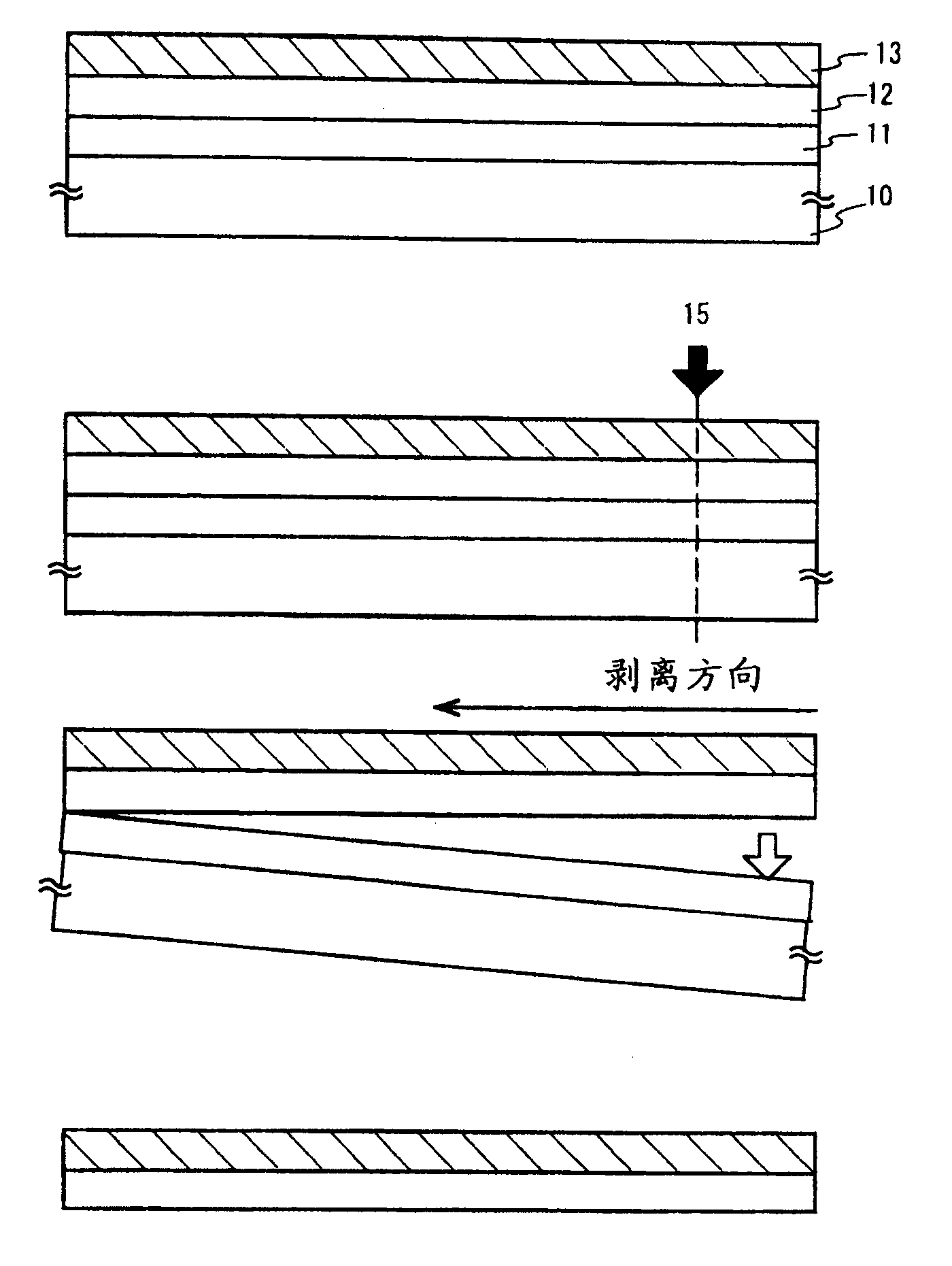
在下文中,将利用附图1A-1D简要描述依照本发明的典型的剥离次序。Hereinafter, a typical peeling sequence according to the present invention will be briefly described using FIGS. 1A-1D.
在图1A中,参考标记10表示基底,11表示具有张应力的第一材料层,12表示具有压应力的第二材料层,而13表示待剥离层。In FIG. 1A ,
在图1A中,玻璃基底、石英基底、陶瓷基底等等可用作基底10。此外,硅基底、金属基底、或不锈钢基底也可替代用作基底10。In FIG. 1A , a glass substrate, a quartz substrate, a ceramic substrate, or the like can be used as the
首先,如图1A所示,在基底10上形成第一材料层11。第一材料层11在刚刚成型之后具有压应力或张应力。重要的是第一材料层由这样的材料形成,其在形成待剥离层时进行热处理或激光辐照不会引起诸如剥离之类的麻烦,并且在刚刚形成待剥离层之后其具有范围为1达因/厘米2至1×1010达因/厘米2的张应力。作为一个典型的例子,有一个单层,其由如下材质制成:选自W、WN、TiN与TiW的元素,或者主要包含这些元素的合金材料或化合物材料,或者它们的叠层。First, as shown in FIG. 1A , a
接下来,第二材料层12形成在第一材料层11上。重要的是第二材料层12由这样的材料形成,其在形成待剥离层时热处理或激光辐照不会引起诸如剥离之类的麻烦,并且在刚刚形成待剥离层之后其具有范围为1达因/厘米2至1×1010达因/厘米2的压应力。作为第二材料层12典型的例子,是氧化硅、氮氧化硅、金属氧化物材料、或它们的叠层。注意第二材料层12可利用任何薄膜形成方法形成,例如溅射方法、等离子体化学汽相淀积方法、或涂敷方法。Next, the
在本发明中,重要的是在第二材料层12中产生压应力而在第一材料层11中产生张应力。相应适合于调整第一材料层11的内应力和第二材料层12的内应力,各自的薄膜厚度优选地设置为1nm~1000nm。此外,可通过热处理或激光辐照调整第一材料层11的内应力和第二材料层12的内应力。In the present invention, it is important to generate compressive stress in the
而且,为了简明描述处理步骤,图1A-1D显示了形成的第一材料层11与基底10相接触的例子。绝缘层或金属层作为缓冲层可设置在基底10和第一材料层11之间,用以提高与基底10的接触性质。Moreover, in order to briefly describe the processing steps, FIGS. 1A-1D show an example in which the formed
接下来,要剥离的层13形成在第二材料层12上(图1A)。要剥离的层13优选地包含各种由TFT(薄膜晶体管)代表的元件(薄膜二极管、具有硅PIN结的光电转换元件、以及硅电阻元件)。此外,只要基底10能够忍耐得住,热处理就可以一直进行。注意,尽管在本发明中第二材料层12的内应力异于第一材料层11的内应力,但也不因形成待剥离层13步骤中的热处理而导致薄膜剥离等。Next, the
接下来,部分地减小第一材料层11和第二材料层12之间的接触性质。此时,进行激光15辐照(图1B)。对于激光而言,优选地选用气体激光器(诸如准分子激光器、CO2激光器、或氩激光器)、固体激光器(诸如玻璃激光器、红宝石激光器、变石激光器、或钛:蓝宝石激光器)、利用晶体的固体激光器(诸如YAG、YVO4、YLF、或YAlO3,其掺杂Nd、Tm或Ho)、或者半导体激光器。此外,激光振荡型式可以是连续振荡也可以是脉冲振荡。激光光束可以具有线形形状、矩形形状、圆形形状、或椭圆形形状。使用波长可以是基波、二次谐波、或三次谐波,且优选地通过操作者选择适当波长。扫描方向可以是纵向、横向、或斜向。而且,可执行往返来回扫描。Next, the contact properties between the
因此,重要的是制备这样一个区域,即,导引(lead),在执行剥离步骤之前该区域易于出现剥离现象。当完成用以选择性地(部分地)减小接触性质的预处理时,避免了坏的剥离情形从而又提高了生产量。Therefore, it is important to prepare an area, ie, a lead, which is prone to peeling before performing the peeling step. When the pre-treatment to selectively (partially) reduce the contact properties is done, bad delamination situations are avoided thereby again increasing throughput.
接下来,由激光辐照的区域开始进行剥离,由此通过物理手段沿着图1C中箭头所示方向剥离其上设置有第一材料层11的基底10(图1C)。Next, the area irradiated by the laser starts to be peeled off, thereby peeling off the
第二材料层12具有压应力而第一材料层11具有张应力。因此,利用较小的力就可剥离基底(例如,利用人的手,利用喷嘴吹出气体的吹压,利用超声,等等)。此外,通过上述激光处理部分地形成具有小接触性质的区域。因此,可以利用较小的力剥离基底。The
而且,该实施例基于如下假设:在此待剥离层13具有足够的机械强度。当待剥离层13机械强度不够大时,优选地在向该处粘结支撑(未示出)(用于稳固待剥离层13)之后剥离基底。Furthermore, this embodiment is based on the assumption that the
因此,可将第二材料层12上形成的待剥离层13与基底10分离。剥离之后得到的情形如图1D所示。Therefore, the layer to be peeled 13 formed on the
而且,在剥离之后可将分离的待剥离层13粘结到转移体(未示出)。Also, the separated to-
而且,本发明可应用于各种半导体器件制造方法中。尤其是,当塑料基底用作转移体和支撑时,可以减轻重量。Also, the present invention can be applied to various semiconductor device manufacturing methods. In particular, when the plastic substrate is used as a transfer body and support, weight savings can be achieved.
当制造液晶显示器件时,优选地将支撑用作反向基底并且利用作为粘合层的密封件粘结到待剥离层。在这种情形下,设置到待剥离层的元件具有象素电极。在象素电极和反向基底之间的空隙内填充液晶材料。此外,制造液晶显示器件的次序是没有特别限定的。例如,将作为支撑的反向基底粘结到设置在基底上的待剥离层,将液晶材料注入其中,而后剥离基底且将作为转移体的塑料基底粘结到待剥离层。或者,在形成象素电极之后,剥离基底,将作为第一转移体的塑料基底粘结到待剥离层,而后将作为第二转移体的反向基底粘结到其上。When manufacturing a liquid crystal display device, it is preferable to use a support as a counter substrate and bond to the layer to be peeled with a sealing member as an adhesive layer. In this case, the element provided to the layer to be peeled off has a pixel electrode. A liquid crystal material is filled in the space between the pixel electrode and the counter substrate. In addition, the order of manufacturing the liquid crystal display device is not particularly limited. For example, a reverse substrate as a support is bonded to a layer to be peeled provided on the substrate, a liquid crystal material is injected thereinto, and then the substrate is peeled off and a plastic substrate as a transfer body is bonded to the layer to be peeled off. Alternatively, after the formation of the pixel electrodes, the substrate is peeled off, the plastic substrate as the first transfer body is bonded to the layer to be peeled off, and then the reverse substrate as the second transfer body is bonded thereto.
而且,当制造以EL发光器件为代表的发光器件时,优选地将支撑用作密封件。因此,发光器件完全与外部屏蔽,以便阻止诸如湿气或氧气这样的物质由外部进入,这些物质会促使有机化合物层变劣。此外,当制造以EL发光器件为代表的发光器件时,就支撑来说,其优选地阻止诸如湿气或氧气这样的物质由外部进入,这些物质会促使有机化合物层变劣。此外,制造发光器件的次序是没有特别限定的。例如,在形成发光器件之后,将作为支撑的塑料基底粘结到设置在基底上的待剥离层,剥离基底,而将作为转移体的塑料基底粘结到待剥离层。或者,在形成发光器件之后,剥离基底,将作为第一转移体的塑料基底粘结到要剥离的层,而后将作为第二转移体的塑料基底粘结到其上。Also, when manufacturing a light emitting device typified by an EL light emitting device, it is preferable to use the support as a sealing member. Therefore, the light emitting device is completely shielded from the outside in order to prevent the entry of substances such as moisture or oxygen from the outside, which promote the deterioration of the organic compound layer. In addition, when manufacturing a light emitting device typified by an EL light emitting device, it is preferable for the support to prevent the entry of substances such as moisture or oxygen from the outside, which promote the deterioration of the organic compound layer. In addition, the order of manufacturing the light emitting devices is not particularly limited. For example, after forming a light emitting device, a plastic substrate as a support is bonded to a layer to be peeled provided on the substrate, the substrate is peeled off, and a plastic substrate as a transfer body is bonded to the layer to be peeled off. Alternatively, after forming the light emitting device, the substrate is peeled off, the plastic substrate as the first transfer body is bonded to the layer to be peeled off, and the plastic substrate as the second transfer body is bonded thereto.
[实施方式2][Embodiment 2]
在这个实施方式中,将利用附图2A-2C简要描述一个实例,其中气体吹到待剥离层端面将待剥离层剥离。In this embodiment, an example in which a gas is blown to the end face of the layer to be peeled to peel off the layer to be peeled will be briefly described using FIGS. 2A to 2C.
在图2A中,参考标记20表示基底,21表示具有张应力的第一材料层,22表示具有压应力的第二材料层,而23表示待剥离层。注意图2A与图1A相同且在此省略了详尽描述。In FIG. 2A,
在通过与实施方式1相同的次序得到图2A中所示状态之后,如图2B中所示,在激光24辐照到一个区域的同时,由喷嘴25高压喷吹出来的气体吹到在基底端面内的第一材料层和第二材料层之间界面,由此沿着图2B中箭头所示方向实施剥离。After the state shown in FIG. 2A is obtained through the same procedure as that of Embodiment 1, as shown in FIG. 2B, while the laser light 24 is irradiating an area, the gas blown out by the nozzle 25 at high pressure is blown onto the end surface of the substrate. The interface between the inner first material layer and the second material layer, thereby performing peeling along the direction indicated by the arrow in FIG. 2B.
这里,是将风压力用作物理手段。但是,无庸费言物理手段没有特别的局限。此外,在这里所示的实例中,利用风压力剥离是与激光24辐照同时进行的。最初可以执行激光辐照以部分减小第一材料层21和第二材料层22之间的接触性质,而后可利用风压力致使实现剥离。Here, wind pressure is used as a physical means. However, it goes without saying that the physical means is not particularly limited. Furthermore, in the example shown here, peeling by wind pressure is performed simultaneously with laser 24 irradiation. Laser irradiation may initially be performed to partially reduce the contact properties between the
而且,像例如氮气或氩气这样一类的惰性气体优选地用作喷吹气体。气体可以在室温下使用或者加热到高温。Furthermore, an inert gas such as eg nitrogen or argon is preferably used as the blowing gas. Gases can be used at room temperature or heated to elevated temperatures.
而且,激光24的辐照可以是沿着剥离方向扫描。此外,喷嘴25可以移动。Also, the irradiation of the laser light 24 may be scanned along the peeling direction. Furthermore, the nozzle 25 can be moved.
第二材料层22具有压应力而第一材料层21具有张应力。因此,可用较小风压力剥离待剥离层。此外,通过上述激光处理步骤部分地形成具有较小接触性质的区域。因此,可用更小的风压力剥离待剥离层。The
而且,该实例基于如下假设:在此示出假设待剥离层23具有足够的机械强度。当待剥离层23机械强度不够大时,优选地在向该处粘结用于稳固要剥离的层23的支撑(未示出),然后剥离它。Also, this example is based on the assumption that it is shown here on the assumption that the
因此,可将第二材料层22上形成的待剥离层23与基底20分离。剥离之后得到的情形如图2C所示。Therefore, the layer to be peeled 23 formed on the
而且,在剥离之后可将分离的待剥离层23粘结到转移体(未示出)。Also, the separated to-
而且,本发明可应用于各种半导体器件制造方法中。尤其是,当塑料基底用作转移体和支撑时,可以减轻重量。Also, the present invention can be applied to various semiconductor device manufacturing methods. In particular, when the plastic substrate is used as a transfer body and support, weight savings can be achieved.
[实施方式3][Embodiment 3]
在这个实施方式中,将利用附图3A-3D简要描述一个实例,其中在剥离之前利用金刚石笔将压力施加到待剥离层,以部分减小接触性质。In this embodiment, an example will be briefly described using FIGS. 3A-3D in which a diamond pen is used to apply pressure to the layer to be peeled before peeling to partially reduce the contact property.
在图3A中,参考标记30表示基底,31表示具有张应力的第一材料层,32表示具有压应力的第二材料层,而33表示待剥离层。注意图3A与图1A相同且在此省略了详尽描述。In FIG. 3A,
在通过与实施方式1相同的次序得到图3A中所示状态之后,如图3B中所示,外力35施加到笔34用以刮擦待剥离层,由此部分地减小第一材料层31和第二材料层32之间的接触性质。这里使用的是金刚石笔。优选地,硬针在负荷作用下垂直按压并移动。After obtaining the state shown in FIG. 3A through the same procedure as Embodiment Mode 1, as shown in FIG. 3B, an
因此,重要的是制备这样一个区域,那即,导引(lead),在执行剥离步骤之前该区域易于出现剥离现象。当完成用以选择性地(部分地)减小接触性质的预处理时,可避免坏的剥离情形从而又提高了生产量。Therefore, it is important to prepare an area, that is, a lead, which is prone to delamination before performing the delamination step. When the pre-treatment to selectively (partially) reduce the contact properties is done, bad peeling situations can be avoided thereby again increasing the throughput.
接下来,由施加负荷的区域开始执行剥离,由此通过物理手段沿着图3C中箭头所示方向剥离其上设置有第一材料层31的基底30(图3C)。Next, peeling is performed from the area where the load is applied, whereby the
第二材料层32具有压应力而第一材料层31具有张应力。因此,可用较小的力剥离基底。此外,通过上述激光处理步骤部分地形成具有小接触性质的区域。因此,可用更小的力剥离基底。The
而且,该实施例基于如下假设:在此示出假设待剥离层33具有足够的机械强度。当待剥离层33机械强度不够大时,优选地在向该处粘结用于稳固待剥离层33的支撑(未示出)之后剥离基底。Also, this embodiment is based on the assumption that it is shown here on the assumption that the
因此,可将第二材料层32上形成的待剥离层33与基底30分离。剥离之后得到的情形如图3D所示。Therefore, the layer to be peeled 33 formed on the
而且,在剥离之后可将分离的待剥离层33粘结到转移体(未示出)。Also, the separated to-
而且,本发明可应用于各种半导体器件制造方法中。尤其是,当塑料基底用作转移体和支撑时,可以减轻重量。Also, the present invention can be applied to various semiconductor device manufacturing methods. In particular, when the plastic substrate is used as a transfer body and support, weight savings can be achieved.
而且,利用金刚石笔执行下述测试。此处,TiN膜用作第一材料层而SiO2膜用作第二材料层。Also, the following tests were performed using a diamond pen. Here, a TiN film is used as the first material layer and a SiO2 film is used as the second material layer.
为了获取试样,通过溅射方法在玻璃基底上形成薄膜厚度100nm的TiN膜,而后通过溅射方法形成薄膜厚度200nm的氧化硅膜。In order to obtain a sample, a TiN film with a film thickness of 100 nm was formed on a glass substrate by a sputtering method, and then a silicon oxide film with a film thickness of 200 nm was formed by a sputtering method.
接下来,通过溅射方法形成薄膜厚度200nm的氧化硅层。关于氧化硅层的形成条件,使用的是RF型溅射设备和氧化硅靶(直径30.5cm)。此外,基底温度设定到150℃,薄膜形成压力设定到0.4Pa,薄膜形成功率设定到3kW,而氩气流速/氧气流速=35sccm/15sccm。Next, a silicon oxide layer was formed with a film thickness of 200 nm by a sputtering method. Regarding the formation conditions of the silicon oxide layer, an RF type sputtering device and a silicon oxide target (30.5 cm in diameter) were used. In addition, the substrate temperature was set to 150° C., the film forming pressure was set to 0.4 Pa, the film forming power was set to 3 kW, and the argon flow rate/oxygen flow rate=35 sccm/15 sccm.
接下来,通过等离子体化学汽相淀积方法在氧化硅层33上形成基体绝缘层。关于该基体绝缘层,通过等离子体化学汽相淀积方法利用SiH4、NH3和N2O作为原料气体在300℃薄膜形成温度下形成薄膜厚度50nm的氮氧化硅薄膜(成分比:Si=32%,O=27%,N=24%,以及H=17%)。用臭氧水清洗表面而后用稀释的氢氟酸(1/100稀释)将表面上形成的氧化物薄膜除去。然后,通过等离子体化学汽相淀积方法利用SiH4和N2O作为原料气体在300℃薄膜形成温度下叠层形成薄膜厚度100nm的氮氧化硅薄膜(成分比:Si=32%,O=59%,N=7%,以及H=2%)。而且,通过等离子体化学汽相淀积方法利用SiH4作为薄膜形成气体(不使其暴露于空气)在300℃薄膜形成温度下形成厚度为54nm的非晶态结构的半导体层(此处,指非晶硅层)。Next, a base insulating layer is formed on the
接下来,将含10ppm镍(按重量折算)的乙酸镍溶液通过旋除机施加到整个表面上。作为替代方法可以使用通过溅射方法将镍元素喷涂到整个表面上的方法。然后,进行热处理用以结晶形成具有结晶结构的半导体薄膜(此处,指多晶硅层)。此时,执行脱氢热处理(500℃持续1小时)而后执行结晶热处理(550℃持续4小时)以得到具有结晶结构的硅膜。注意,这里使用了利用镍作为促进硅结晶的金属元素结晶技术。另外也可以使用像例如固相方法或激光结晶方法那样的已知结晶技术。Next, a nickel acetate solution containing 10 ppm nickel (by weight) was applied to the entire surface by a spinner. Alternatively, a method of spraying nickel element onto the entire surface by a sputtering method may be used. Then, heat treatment is performed to crystallize and form a semiconductor thin film (here, a polysilicon layer) having a crystalline structure. At this time, dehydrogenation heat treatment (500° C. for 1 hour) and then crystallization heat treatment (550° C. for 4 hours) were performed to obtain a silicon film having a crystalline structure. Note that a crystallization technique using nickel as a metal element to promote crystallization of silicon is used here. It is also possible to use known crystallization techniques such as, for example, solid-phase methods or laser crystallization methods.
接下来,用金刚石笔刻划图4A中所示负荷线41。负荷线是任意的且设定平行于基底的端表面,位于待剥离区域42中。此时,剥离与基底端表面接触的设置给基底的多晶硅层区域。Next, the
接下来,将粘结带粘结到待剥离区域(多晶硅层)。Next, an adhesive tape is bonded to the area to be peeled off (polysilicon layer).
接下来,通过人手沿着图4B中箭头所示方向(剥离方向)产生张力以便从基底分离出粘结带。剥离之后所得到的基底的情形如图4B所示,而剥离之后所得到的粘结带的情形如图4C所示。在带中可以显著地观察到剥离区域43。Next, tension is generated by hand in the direction indicated by the arrow in FIG. 4B (peeling direction) to separate the adhesive tape from the substrate. The state of the obtained substrate after peeling is shown in FIG. 4B , and the state of the obtained adhesive tape after peeling is shown in FIG. 4C . The stripped
作为对比,不经金刚石笔刻划而粘结该粘结带而后执行剥离。结果是,如图17A所示,尽管也用粘结带粘结到待剥离区域51,却有残留未剥离区域53(图17B)产生在基底上。因此,如图17C所示,剥离区域54部分地产生在带中,由此导致坏的剥离情形。For comparison, the adhesive tape was bonded without diamond pen scoring and then peeled off. As a result, as shown in FIG. 17A, a residual non-peeled region 53 (FIG. 17B) is produced on the substrate although it is also bonded to the region 51 to be peeled with an adhesive tape. Therefore, as shown in FIG. 17C, a peeling
导致坏的剥离情形的原因如下。那即,与基底中心区域相比,具有小薄膜厚度的区域易于形成在基底的外缘区域。如果薄膜厚度很小,则形成具有高的基底接触性质的区域且变得很难剥离。The reasons for the bad peeling situation are as follows. That is, a region with a small film thickness is easily formed in the peripheral region of the substrate as compared with the central region of the substrate. If the film thickness is small, a region with high substrate contact properties is formed and it becomes difficult to peel off.
因此,重要的是预先制备导引,这样在剥离之前易于产生剥离现象。执行用于选择性(部分地)减少接触性质的预处理,可从基底的整个表面上剥离待剥离层。Therefore, it is important to prepare the guide in advance so that the peeling phenomenon is easy to occur before peeling. Performing pretreatment for selectively (partially) reducing the contact properties, the layer to be peeled can be peeled off from the entire surface of the substrate.
此处,在粘结粘结带之前用金刚石笔进行刻划。用金刚石笔的刻划也可以在粘结粘结带之后进行。Here, scoring was performed with a diamond pen prior to bonding the adhesive tape. Scribing with a diamond pen can also be done after bonding the adhesive tape.
而且,这里所示实例中,利用第一材料层(TiN层)和第二材料层(SiO2层)执行剥离。但是,剥离方法并不特别局限于此。例如,在提供由非晶硅(或多晶硅)制成的分离层、且通过基底向那里辐照激光、以释放非晶硅薄膜中所含的氢、由此产生间隙用以分离基底和待剥离层的这样一个方法中,当在剥离之前仅仅对基底外缘区域附近执行用于选择性(部分地)减少接触性质的预处理时,可以完成剥离,而不出现未充分剥离。Also, in the example shown here, lift-off was performed using the first material layer (TiN layer) and the second material layer (SiO 2 layer). However, the peeling method is not particularly limited thereto. For example, when a separation layer made of amorphous silicon (or polysilicon) is provided, and laser light is irradiated thereto through the substrate, hydrogen contained in the amorphous silicon film is released, thereby creating a gap for separating the substrate and the substrate to be peeled off. In such a method of the layer, when the pretreatment for selectively (partially) reducing the contact properties is performed only in the vicinity of the outer edge region of the substrate before the peeling, the peeling can be completed without insufficient peeling.
接下来,当TiN、W、WN、Ta或TaN用作第一材料层材质时,设置第二材料层(氧化硅:200nm薄膜厚度)与第一材料层相接触。然后,执行下面的测试以检测设置在第二材料层上的待剥离层是否能从基底剥离。Next, when TiN, W, WN, Ta or TaN is used as the material of the first material layer, a second material layer (silicon oxide: 200 nm film thickness) is provided in contact with the first material layer. Then, the following test was performed to check whether the layer to be peeled provided on the second material layer could be peeled from the substrate.
为了得到试样1,通过溅射方法在玻璃基底上形成薄膜厚度100nm的TiN薄膜,然后通过溅射方法形成薄膜厚度200nm的氧化硅薄膜。形成氧化硅薄膜之后,如上述测试中所述的那样进行叠层和结晶。To obtain Sample 1, a TiN film with a film thickness of 100 nm was formed on a glass substrate by a sputtering method, and then a silicon oxide film was formed with a film thickness of 200 nm by a sputtering method. After forming the silicon oxide film, lamination and crystallization were performed as described in the above test.
为了得到试样2,通过溅射方法在玻璃基底上形成薄膜厚度50nm的W薄膜,然后通过溅射方法形成薄膜厚度200nm的氧化硅薄膜。形成氧化硅薄膜之后,如上述测试中所述的那样进行叠层和结晶。In order to obtain Sample 2, a W film with a film thickness of 50 nm was formed on a glass substrate by a sputtering method, and then a silicon oxide film with a film thickness of 200 nm was formed by a sputtering method. After forming the silicon oxide film, lamination and crystallization were performed as described in the above test.
为了得到试样3,通过溅射方法在玻璃基底上形成薄膜厚度50nm的WN薄膜,然后通过溅射方法形成薄膜厚度200nm的氧化硅薄膜。形成氧化硅薄膜之后,如上述测试中所述的那样进行叠层和结晶。In order to obtain Sample 3, a WN film with a film thickness of 50 nm was formed on a glass substrate by a sputtering method, and then a silicon oxide film was formed with a film thickness of 200 nm by a sputtering method. After forming the silicon oxide film, lamination and crystallization were performed as described in the above test.
为了得到试样4,通过溅射方法在玻璃基底上形成薄膜厚度50nm的TiN薄膜,然后通过溅射方法形成薄膜厚度200nm的氧化硅薄膜。形成氧化硅薄膜之后,如上述测试中所述的那样进行叠层和结晶。In order to obtain Sample 4, a TiN film with a film thickness of 50 nm was formed on a glass substrate by a sputtering method, and then a silicon oxide film was formed with a film thickness of 200 nm by a sputtering method. After forming the silicon oxide film, lamination and crystallization were performed as described in the above test.
为了得到试样5,通过溅射方法在玻璃基底上形成薄膜厚度50nm的Ta薄膜,然后通过溅射方法形成薄膜厚度200nm的氧化硅薄膜。形成氧化硅薄膜之后,如上述测试中所述的那样进行叠层和结晶。In order to obtain Sample 5, a Ta film with a film thickness of 50 nm was formed on a glass substrate by a sputtering method, and then a silicon oxide film was formed with a film thickness of 200 nm by a sputtering method. After forming the silicon oxide film, lamination and crystallization were performed as described in the above test.
为了得到试样6,通过溅射方法在玻璃基底上形成薄膜厚度50nm的TaN薄膜,然后通过溅射方法形成薄膜厚度200nm的氧化硅薄膜。形成氧化硅薄膜之后,如上述测试中所述的那样进行叠层和结晶。In order to obtain Sample 6, a TaN film with a film thickness of 50 nm was formed on a glass substrate by a sputtering method, and then a silicon oxide film was formed with a film thickness of 200 nm by a sputtering method. After forming the silicon oxide film, lamination and crystallization were performed as described in the above test.
这样,得到了试样1至6。关于每个试样,都是利用金刚石笔刻划它的一部分,然后将粘结带粘结到待剥离层,且执行检验待剥离层是否剥离的测试。结果见表1。In this way, Samples 1 to 6 were obtained. With respect to each test piece, a part thereof was scratched with a diamond pen, an adhesive tape was bonded to the layer to be peeled, and a test for checking whether the layer to be peeled was peeled was performed. The results are shown in Table 1.
表1Table 1
而且,关于氧化硅薄膜、TiN薄膜、W薄膜、以及Ta薄膜,在热处理(550℃持续4小时)前后测量其各自的内应力。结果见表2。Also, regarding the silicon oxide film, the TiN film, the W film, and the Ta film, their respective internal stresses were measured before and after heat treatment (550° C. for 4 hours). The results are shown in Table 2.
表2Table 2
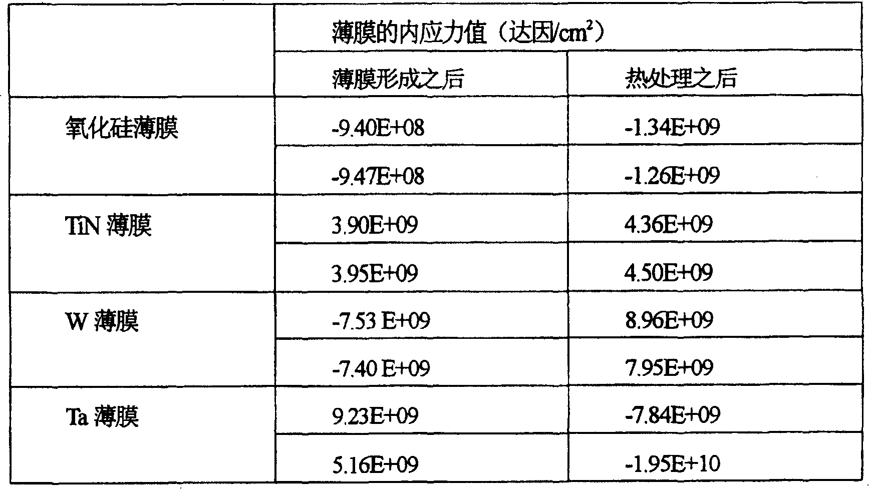
注意,执行测量所针对的氧化硅薄膜薄膜厚度400nm、通过溅射方法形成在硅基底上。此外,TiN薄膜、W薄膜、以及Ta薄膜都是通过溅射方法形成在玻璃基底上,薄膜厚度400nm,而后测量各自的内应力。之后,叠层氧化硅薄膜作为覆盖薄膜并进行热处理,然后通过蚀刻去除该覆盖薄膜,并且再次测量各自的内应力。此外,为相应的薄膜制造两个试样并且进行测量。Note that the silicon oxide film for which the measurement was performed was formed on a silicon substrate by a sputtering method with a film thickness of 400 nm. In addition, the TiN thin film, W thin film, and Ta thin film were all formed on the glass substrate by sputtering, with a film thickness of 400nm, and then the respective internal stresses were measured. After that, a silicon oxide film was stacked as a cover film and heat-treated, and then the cover film was removed by etching, and the respective internal stresses were measured again. In addition, two samples were produced for the corresponding films and measured.
W薄膜在形成之后即刻就具有压应力(大约-7×10⁹达因/cm2)。但是,经过热处理之后它变得具有张应力了(大约8×109达因/cm2至9×109达因/cm2)。因此,得到了优选的剥离状态。关于TiN薄膜,其应力在热处理前后大致相同,并且它具有张应力(大约3.9×109达因/cm2至4.5×109达因/cm2)。当薄膜厚度是50nm或更小时,则导致坏的剥离。此外,关于Ta薄膜,它在形成之后即刻就具有张应力(大约5.1×109达因/cm2至9.2×109达因/cm2)。但是,经过热处理之后该薄膜变得具有压应力了(大约-2×109达因/cm2至-7.8×109达因/cm2)。因此,在带测试中不产生剥离。此外,关于硅薄膜,其应力在热处理前后大致相同,并且它具有压应力(大约-9.4×108达因/cm2至-1.3×109达因/cm2)。The W thin film has compressive stress (approximately -7×10 9 dynes/cm 2 ) immediately after formation. However, after heat treatment it becomes tensile (approximately 8×10 9 dyne/cm 2 to 9×10 9 dyne/cm 2 ). Therefore, a preferred peeled state is obtained. Regarding the TiN thin film, its stress is approximately the same before and after heat treatment, and it has a tensile stress (approximately 3.9×10 9 dyne/cm 2 to 4.5×10 9 dyne/cm 2 ). When the film thickness is 50 nm or less, bad peeling results. Furthermore, regarding the Ta thin film, it has tensile stress (approximately 5.1×10 9 dyne/cm 2 to 9.2×10 9 dyne/cm 2 ) immediately after formation. However, the film became compressively stressed (approximately -2×10 9 dyne/cm 2 to -7.8×10 9 dyne/cm 2 ) after heat treatment. Therefore, no peeling occurred in the tape test. Furthermore, regarding the silicon thin film, its stress is approximately the same before and after heat treatment, and it has compressive stress (approximately -9.4×10 8 dyne/cm 2 to -1.3×10 9 dyne/cm 2 ).
由这些结果,剥离现象与归因于各种因素的接触性质有关。尤其是,其与内应力很有关。当使用具有压应力的第二材料层且将具有经过热处理获得的张应力的薄膜用作第一材料层时,可以理解待剥离层能够从基底整个表面地剥离出。此外,在通过热处理或激光辐照改变张应力的情形下,希望的是,用作第一材料层的材料与热处理或激光辐照之前相比张应力值增大。From these results, the peeling phenomenon is related to the contact properties attributed to various factors. In particular, it is very much related to internal stress. When a second material layer having compressive stress is used and a film having tensile stress obtained through heat treatment is used as the first material layer, it is understood that the layer to be peeled can be peeled off from the entire surface of the substrate. Furthermore, in the case of changing the tensile stress by heat treatment or laser irradiation, it is desirable that the material used as the first material layer has an increased tensile stress value compared to before the heat treatment or laser irradiation.
而且,尤其当第一材料层或第二材料层薄时,本发明中在剥离之前用于部分地减少接触性质的处理步骤是有效的。这是因为如果薄膜厚度小,在薄膜形成时基底上的厚度分布易于变化,并且薄膜的内应力、薄膜质量等等都易于改变,由此难于剥离。为了提高生产量,优选地将第一材料层或第二材料层的薄膜厚度减低为最小。Also, especially when the first material layer or the second material layer is thin, the processing step in the present invention for partially reducing the contact property before peeling is effective. This is because if the film thickness is small, the thickness distribution on the substrate is apt to change at the time of film formation, and internal stress of the film, film quality, etc. are apt to change, thereby making peeling difficult. In order to increase throughput, it is preferable to minimize the film thickness of the first material layer or the second material layer.
将通过下述实施例详尽描述具有上述结构的本发明。The present invention having the above structure will be described in detail by the following examples.
[实施例1][Example 1]
参照附图5A-7描述本发明的一个实施例。这里,详尽地描述同时制造象素部分和设置在同一基底上象素部分周边中的驱动电路的TFT(n沟道TFT和p沟道TFT)的方法。An embodiment of the present invention is described with reference to Figures 5A-7. Here, a method of simultaneously manufacturing a pixel portion and TFTs (n-channel TFT and p-channel TFT) of a driver circuit provided in the periphery of the pixel portion on the same substrate is described in detail.
首先,在基底100上形成第一材料层101、第二材料层102、基体绝缘膜103并得到具有结晶结构的半导体薄膜。然后,蚀刻半导体薄膜具有所希望形状以形成半导体层104至108,它们彼此分离呈孤岛型态。First, a
将玻璃基底(#1737)用作基底100。A glass substrate (#1737) was used as the
只要用作第一材料层101的材料刚好在稍后进行的剥离步骤之前具有在1到1×10¹⁰(达因/厘米2)的范围内的张应力,该材料并不特别局限于特定材料。下述材料的层或层叠层可用于第一材料层101;金属材料(Ti、Al、Ta、W、Mo、Cu、Cr、Nd、Fe、Ni、Co、Zr、Zn、Ru、Rh、Pd、Os、Ir、以及Pt等)、半导体材料(例如Si或Ge等)、绝缘材料或有机材料。这里,使用通过溅射方法层积而成的100nm厚的氮化钛薄膜。As long as the material used as the
只要用作第二材料层102的材料刚好在稍后进行的剥离步骤之前具有在-1到-1×10¹⁰(达因/厘米2)的范围内的压应力,该材料并不特别局限于特定材料。下述材料的层或层叠层可用于第二材料层102;金属材料(Ti、Al、Ta、W、Mo、Cu、Cr、Nd、Fe、Ni、Co、Zr、Zn、Ru、Rh、Pd、Os、Ir、以及Pt等)、半导体材料(例如Si或Ge等)、绝缘材料或有机材料。这里,可以使用由氧化硅材料或金属氧化物材料构成的单层或层叠层。使用通过溅射方法层积而成的200nm厚的氧化硅薄膜。第一材料层101和第二材料层102之间的粘结力强于热处理作用,所以薄膜剥离(也称为剥离)等不会出现。但是,通过物理手段在第二材料层内部或界面上剥离易于实现。As long as the material used for the
对于基体绝缘膜103,由SiH4、NH3和N2O作为原料气体(成分比:Si=32%,O=27%,N=24%,H=17%)形成的氮氧化硅膜103a形成厚度为50nm(优选地为10-200nm),且是通过利用等离子体化学汽相淀积方法在400℃薄膜淀积温度下形成的。然后,在利用臭氧水清洗表面之后,用稀释的氢氟酸(1/100稀释)将表面上形成的氧化物薄膜除去。接下来,利用SiH4和N2O作为原料气体(成分比:Si=32%,O=59%,N=7%,H=2%)在其上形成的氮氧化硅膜103b,形成厚度为100nm(优选地为50-200nm),且是通过利用等离子体化学汽相淀积方法在400℃薄膜淀积温度下形成的,由此形成叠层结构。而且,不使其暴露于空气的情况下,利用SiH4作为薄膜淀积气体、且通过利用等离子体化学汽相淀积方法在300℃薄膜淀积温度下而形成54nm厚的(优选地为25-80nm)非晶态结构的半导体薄膜(在这个实施例中,指非晶硅薄膜)。For the
在这个实施例中,基体膜103显示为双层结构形式,但可以使用单层的上述绝缘薄膜或者两层或多层叠层的结构。而且,对于半导体薄膜材质没有限制。但是,半导体薄膜可优选地由硅或硅锗(SiXGe1-X(X=0.0001~0.02))合金通过已知方法(溅射、LPCVD、等离子体化学汽相淀积方法等)形成。而且,等离子体化学汽相淀积设备可以是单晶片型或批量型。此外,可在同一薄膜形成室中不暴露于空气的情况下连续形成基体绝缘膜和半导体薄膜。In this embodiment, the
随即,在清洗具有非晶结构地半导体薄膜的表面之后,由表面上的臭氧水形成非常薄的厚度约为2nm的氧化物薄膜。然后,为了控制TFT的阈值,掺杂极小量的杂质元素(硼或磷)。这里,利用离子掺杂方法,其中没有质量分离地等离子体激发乙硼烷(B2H6),并且在下述掺杂条件下将硼添加到非晶硅薄膜:加速电压15kV;利用30sccm的氢气将乙硼烷稀释到1%的气体流速;以及2×10¹²/cm2的剂量。Then, after cleaning the surface of the semiconductor thin film having an amorphous structure, a very thin oxide film with a thickness of about 2 nm was formed from the ozone water on the surface. Then, in order to control the threshold of the TFT, an extremely small amount of impurity element (boron or phosphorus) is doped. Here, an ion doping method is used in which diborane (B 2 H 6 ) is plasma-excited without mass separation, and boron is added to the amorphous silicon thin film under the following doping conditions: accelerating
然后,利用旋涂器喷施含有10ppm(重量)镍的乙酸镍盐溶液。作为本发明的替换方法,也可以使用通过溅射将镍元素喷涂到整个表面上的方法。Then, a nickel acetate salt solution containing 10 ppm by weight of nickel was sprayed using a spinner. As an alternative method of the present invention, a method of spraying nickel element onto the entire surface by sputtering may also be used.
然后,执行热处理实现结晶化,由此形成具有结晶结构的半导体薄膜。利用电炉或强光辐照的热处理可用于实现这个热处理。在利用电炉实施热处理的情形下,在500~650℃下执行4~24小时。这里,在执行脱氢热处理(500℃下1小时)之后,执行结晶热处理(550℃下4小时),由此得到具有结晶结构的硅薄膜。注意,尽管这里结晶是通过利用电炉进行热处理来实现的,结晶也可以借助于灯热处理设备来实现。还应注意,尽管这里应用了利用镍作为促进硅结晶的金属元素的结晶技术,但也可以应用其它的已知结晶技术,例如,固相生长方法和激光结晶方法。Then, heat treatment is performed to effect crystallization, thereby forming a semiconductor thin film having a crystalline structure. Heat treatment using an electric furnace or intense light irradiation can be used to achieve this heat treatment. In the case of performing heat treatment using an electric furnace, it is performed at 500 to 650° C. for 4 to 24 hours. Here, after performing dehydrogenation heat treatment (1 hour at 500° C.), crystallization heat treatment (4 hours at 550° C.) was performed, whereby a silicon thin film having a crystalline structure was obtained. Note that although crystallization is carried out here by heat treatment using an electric furnace, crystallization can also be carried out by means of lamp heat treatment equipment. It should also be noted that although a crystallization technique using nickel as a metal element promoting crystallization of silicon is applied here, other known crystallization techniques such as a solid phase growth method and a laser crystallization method may also be applied.
接下来,在利用稀释的氢氟酸等将具有结晶结构的硅薄膜表面上的氧化膜去除之后,在空气中或在氧气环境下辐照第一激光(XeCl:波长308nm)以提高结晶率并且修复晶粒中存在的缺陷。波长400nm或更小的准分子激光、或YAG激光器的二次谐波或三次谐波用作该激光。在这个实施例中,使用重复频率约为10~1000Hz的脉冲激光,通过光学系统将激光浓聚到100~500mJ/cm2,并且以90~95%的重叠率进行辐照,由此可扫描硅薄膜表面。这里,第一激光辐照是在空气中进行的,重复频率为30Hz而能量密度为393mJ/cm2。注意,因为第一激光辐照是在空气中或在氧气环境下进行的,所以通过第一激光辐照在表面上形成了氧化膜。还应注意,尽管这里描述的是一个利用脉冲激光的例子,但是也可以使用连续振荡的激光器。当非晶半导体薄膜结晶的时候,优选地使用固体激光器,其能够连续振荡并且应用二次谐波至四次谐波以便得到大颗粒尺寸的晶体。典型地,只需要施加Nd:YVO4激光器(基波为1064nm)的二次谐波(532nm)和三次谐波(355nm)。当使用连续振荡激光器时,利用非线性光学器件将由输出功率10W的连续振荡YVO4激光器入射的激光转换为谐波。而且,还有一种利用将YVO4晶体和非线性光学器件放置进入谐振腔中实现谐波入射的方法。优选地,激光在辐照表面上成形为矩形或椭圆形,并且将该激光辐照到被处理基底。此时能量密度需要大约为0.01~100MW/cm2(理想地为0.1~10MW/cm2)。相对于激光以10~2000cm/s速度相对移动半导体薄膜,并且辐照激光。Next, after removing the oxide film on the surface of the silicon thin film having a crystalline structure with diluted hydrofluoric acid or the like, the first laser light (XeCl:
接下来,在利用稀释的氢氟酸将因第一激光辐照而形成的氧化膜去除之后,在氮气环境下或真空中执行第二激光辐照,由此夷平半导体薄膜表面。波长400nm或更小的准分子激光、或者YAG激光的二次谐波或三次谐波用作该激光(第二激光)。第二激光的能量密度大于第一激光的能量密度,优选地较之大了30~60mJ/cm2。这里,执行第二激光辐照所用的重复频率为30Hz而能量密度为453mJ/cm2,由此设定半导体薄膜表面不均匀度的P-V值(峰对谷,高度最大值和最小值之间的差值)为50nm或更小。这里,可通过AFM(原子力显微镜)得到不均匀度的P-V值。Next, after removing the oxide film formed by the first laser irradiation with diluted hydrofluoric acid, second laser irradiation is performed in a nitrogen atmosphere or in a vacuum, thereby flattening the surface of the semiconductor thin film. An excimer laser with a wavelength of 400 nm or less, or a second or third harmonic of YAG laser is used as the laser (second laser). The energy density of the second laser is greater than that of the first laser, preferably 30-60 mJ/cm 2 . Here, the repetition frequency for performing the second laser irradiation is 30 Hz and the energy density is 453 mJ/cm 2 , thereby setting the PV value (peak to valley, height between the maximum value and the minimum value) of the unevenness of the semiconductor thin film. difference) of 50nm or less. Here, the PV value of the unevenness can be obtained by AFM (atomic force microscope).
而且,在这个实施例中尽管是在整个表面上执行第二激光辐照,但是至少在象素部分可以采用选择性实施辐照的步骤,这是因为关断电流(off current)的减小尤其对象素部分的TFT有影响。Also, although the second laser irradiation is performed on the entire surface in this embodiment, the step of selectively performing irradiation can be adopted at least in the pixel portion, because the reduction of the off current (off current) is especially Affects the TFT of the pixel part.
接下来,用臭氧水对表面进行处理120秒,由此形成由总厚度为1~5nm的氧化膜构成的阻挡层(barrier layer)。Next, the surface was treated with ozone water for 120 seconds, thereby forming a barrier layer composed of an oxide film with a total thickness of 1 to 5 nm.
然后,含有氩元素(其变为吸气点)的非晶硅薄膜通过溅射形成在阻挡层上以具有150nm厚度。在这个实施例中溅射的薄膜淀积条件是:薄膜淀积压为0.3Pa;气体(Ar)流速为50sccm;薄膜淀积功率为3kW;以及基底温度是150℃。注意在上述条件下,包含在非晶硅薄膜中的氩元素原子浓度是3×10²⁰/cm3~6×1020/cm3,并且氧气的原子浓度是1×1019/cm3~3×1019/cm3。之后,利用灯热处理设备执行热处理在650℃下持续3分钟,用以除气。Then, an amorphous silicon thin film containing argon element which becomes a gettering point was formed on the barrier layer by sputtering to have a thickness of 150 nm. The film deposition conditions by sputtering in this example were: film deposition pressure 0.3 Pa; gas (Ar)
随后,利用阻挡层作为蚀刻阻挡选择性地去除含有氩元素(其为吸气点)的非晶硅薄膜,而后,利用稀释的氢氟酸选择性地去除阻挡层。注意存在这样一种趋势,在除气过程中镍趋于移向具有高浓度氧的区域,且因此,理想地是在除气之后去除包括氧化膜的阻挡层。Subsequently, the amorphous silicon thin film containing argon element (which is a getter point) is selectively removed using the barrier layer as an etching barrier, and then, the barrier layer is selectively removed using diluted hydrofluoric acid. Note that there is a tendency that nickel tends to move to a region with a high concentration of oxygen during degassing, and therefore, it is desirable to remove the barrier layer including the oxide film after degassing.
然后,在得到的具有结晶结构的硅膜(也称为多晶硅薄膜)表面上由臭氧水形成薄的氧化膜之后,形成由抗蚀剂组成的掩模,并且执行蚀刻处理步骤由此得到所期望的形状,由此形成彼此分割开的岛状半导体层104~108。在形成半导体层之后,去除由抗蚀剂组成的掩模。Then, after forming a thin oxide film by ozone water on the surface of the obtained silicon film having a crystalline structure (also referred to as a polysilicon film), a mask composed of a resist is formed, and an etching treatment step is performed to thereby obtain the desired shape, thereby forming island-shaped semiconductor layers 104 to 108 separated from each other. After forming the semiconductor layer, the mask consisting of resist is removed.
然后,利用含有氢氟酸的蚀刻剂去除氧化膜,且同时,清洗硅膜表面。之后,形成以硅为主要组分的绝缘膜,其变为栅绝缘薄膜109。在这个实施例中,通过等离子体化学汽相淀积方法形成薄膜厚度115nm的氮氧化硅薄膜(成分比:Si=32%,O=59%,N=7%,H=2%)。Then, the oxide film is removed with an etchant containing hydrofluoric acid, and at the same time, the surface of the silicon film is cleaned. After that, an insulating film having silicon as a main component, which becomes the
接下来,如图5A所示,在栅绝缘薄膜109上,以叠层形式形成厚度为20~100nm的第一导电薄膜110a和厚度为100~400nm的第二导电薄膜110b。在这个实施例中,顺次将50nm厚的氮化钽薄膜和370nm厚的钨薄膜叠层在栅绝缘薄膜109上。Next, as shown in FIG. 5A , on the
作为构成第一导电薄膜和第二导电薄膜的导电材料,使用选自由Ta、W、Ti、Mo、Al及Cu构成的组的元素、或者包含上述元素作为其主要成分的合金材料或化合物材料。而且,以掺杂有诸如磷的杂质元素的多晶硅薄膜为代表的半导体薄膜、或AgPdCu合金,可以用作第一导电薄膜和第二导电薄膜。而且,本发明不局限于双层结构。例如,可以使用三层结构,其中顺次叠层有50nm厚的钨薄膜、500nm厚的铝硅合金(Al-Si)薄膜、以及30nm厚的氮化钛薄膜。而且,在使用三层结构的情形下,可以用氮化钨替代第一导电薄膜的钨,可以用铝钛合金(Al-Ti)薄膜替代第二导电薄膜的铝硅合金(Al-Si)薄膜,并且可以用钛薄膜替代第三导电薄膜的氮化钛薄膜。此外,也可以使用单层结构。As the conductive material constituting the first conductive thin film and the second conductive thin film, an element selected from the group consisting of Ta, W, Ti, Mo, Al, and Cu, or an alloy material or compound material containing the above element as its main component is used. Also, a semiconductor film represented by a polysilicon film doped with an impurity element such as phosphorus, or an AgPdCu alloy can be used as the first conductive film and the second conductive film. Also, the present invention is not limited to a bilayer structure. For example, a three-layer structure may be used in which a 50 nm-thick tungsten thin film, a 500 nm-thick aluminum-silicon alloy (Al-Si) thin film, and a 30 nm-thick titanium nitride thin film are stacked in this order. Also, in the case of using a three-layer structure, tungsten nitride can be used instead of tungsten for the first conductive film, and aluminum-titanium alloy (Al-Ti) thin film can be used instead of aluminum-silicon alloy (Al-Si) thin film for the second conductive film. , and the titanium nitride film of the third conductive film may be replaced with a titanium film. In addition, a single-layer structure may also be used.
接下来,如图5B所示,通过曝光步骤形成掩模112-117,并且执行用以形成栅电极和布线的第一蚀刻步骤。利用第一和第二蚀刻条件实施第一蚀刻步骤。ICP(感应耦合等离子体)蚀刻方法可优选地用作蚀刻处理。使用ICP蚀刻方法,并且蚀刻条件(施加到线圈形电极的电能,施加到基底侧电极的电能,基底侧上电极的温度,等等)被适当调整,由此可以将薄膜蚀刻得到所期望的锥形形状。注意,以Cl2、BCl3、SiCl4、CCl4等等为代表的氯基气体,以CF4、SF6、NF3等等为代表的氟基气体,以及O2可以适当地用作蚀刻气体。Next, as shown in FIG. 5B, masks 112-117 are formed through an exposure step, and a first etching step to form gate electrodes and wirings is performed. A first etching step is performed using first and second etching conditions. An ICP (Inductively Coupled Plasma) etching method can be preferably used as the etching treatment. The ICP etching method is used, and the etching conditions (electrical energy applied to the coil-shaped electrode, electric energy applied to the substrate side electrode, temperature of the electrode on the substrate side, etc.) are appropriately adjusted, whereby the film can be etched to obtain the desired cone shaped shape. Note that chlorine-based gases represented by Cl 2 , BCl 3 , SiCl 4 , CCl 4 , etc., fluorine-based gases represented by CF 4 , SF 6 , NF 3 , etc., and O 2 can be suitably used for etching gas.
在这个实施例中,还将150W的RF(13.56MHZ)功率施加到基底(试样台)实质上用以施加负的自偏压。还应注意到,在基底侧电极区域的尺寸是12.5cm×12.5cm,而线圈型电极区域(这里,指其上设置有线圈的石英圆状物)的尺寸是直径25cm的圆盘。利用第一蚀刻条件,蚀刻W薄膜以使第一导电层的端面区域形成为锥形形状。在第一蚀刻条件下,W的蚀刻速度是200.39nm/min,TaN的蚀刻速度是80.32nm/min,而W与TaN的选择比大约是2.5。而且,利用第一蚀刻条件,W的锥角大致为26°。之后,将第一蚀刻条件改变为第二蚀刻条件而不去除由抗蚀剂组成的掩模112~117。CF4和Cl2用作蚀刻气体,该气体流速设定为30/30sccm,而将500W的RF(13.56MHZ)功率施加到以1Pa压力生成等离子体的线圈形电极,由此实施蚀刻约30秒钟。还将20W的RF(13.56MHZ)功率施加到基底侧(试样台)实质上用以施加负的自偏压。在混合使用CF4和Cl2的第二蚀刻条件下,W薄膜和TaN薄膜两者都是以同一电平蚀刻的。利用第二蚀刻条件,W的蚀刻速度是58.97nm/min,而TaN的蚀刻速度是66.43nm/min。注意蚀刻时间可增加10~20%以便执行刻蚀后不留残余在栅绝缘薄膜上。In this example, 150 W of RF (13.56 MHZ) power was also applied to the substrate (sample stage) to essentially apply a negative self-bias. It should also be noted that the size of the electrode area on the base side is 12.5 cm x 12.5 cm, while the size of the coil type electrode area (here, referring to the quartz disc on which the coil is placed) is a disc with a diameter of 25 cm. Using the first etching condition, the W film is etched so that the end face region of the first conductive layer is formed into a tapered shape. Under the first etching condition, the etching rate of W is 200.39 nm/min, the etching rate of TaN is 80.32 nm/min, and the selectivity ratio of W to TaN is about 2.5. Also, with the first etching condition, the taper angle of W is approximately 26°. After that, the first etching condition is changed to the second etching condition without removing the
在上述第一蚀刻处理过程中,制造适当的由抗蚀剂组成的掩模形状,借此第一导电层的端面区域和第二导电层的端面区域都具有锥形形状,这归因于施加到基底侧的偏压的作用。锥形部分角度设置范围为15~45°。During the above-mentioned first etching process, an appropriate mask shape composed of a resist is produced, whereby both the end face area of the first conductive layer and the end face area of the second conductive layer have a tapered shape, which is attributed to the application of to the effect of the bias voltage on the basal side. The angle setting range of the tapered part is 15° to 45°.
因此,通过第一蚀刻处理过程形成了由第一导电层和第二导电层(第一导电层119a~123a和第二导电层119b~123b)组成的第一形状导电层119~123。将变为栅绝缘薄膜的绝缘薄膜109蚀刻大约10~20nm,并且变为栅绝缘薄膜118,其中第一形状导电层119~123未覆盖的区域被减薄。Accordingly, the first shape
接下来,执行第二蚀刻处理过程,不去除由抗蚀剂组成的掩模。这里,SF6、Cl2和O2用作刻蚀气体,气体流速设定为24/12/24(sccm),且将700W的RF(13.56MHZ)功率施加到以1.3Pa压力生成等离子体的线圈形电极,由此蚀刻执行25秒钟。还将10W的RF(13.56MHZ)功率施加到基底侧(试样台)实质上用以施加负的自偏压。在第二蚀刻处理过程中,W的蚀刻速度是227.3nm/min,TaN的蚀刻速度是32.1nm/min,W与TaN的选择比是7.1,SiON(绝缘薄膜118)的蚀刻速度是33.7nm/min,而W与SiON的选择比是6.83。在SF6用作蚀刻气体的情形下,如上所述关于绝缘薄膜118的选择比很高。因此,可以抑制薄膜厚度的减小。在这个实施例中,绝缘薄膜118的薄膜厚度仅仅减小约8nm。Next, a second etching process is performed without removing the mask composed of resist. Here, SF 6 , Cl 2 and O 2 were used as etching gas, the gas flow rate was set at 24/12/24 (sccm), and 700 W of RF (13.56 MHZ) power was applied to the Coil-shaped electrodes, whereby etching is performed for 25 seconds. 10 W of RF (13.56 MHZ) power was also applied to the substrate side (sample stage) to essentially apply a negative self-bias. In the second etching process, the etching rate of W is 227.3nm/min, the etching rate of TaN is 32.1nm/min, the selectivity ratio of W and TaN is 7.1, and the etching rate of SiON (insulating film 118) is 33.7nm/min. min, and the selection ratio of W to SiON is 6.83. In the case where SF 6 is used as the etching gas, the selectivity with respect to the insulating
通过第二蚀刻处理过程,W的锥角变为70°。通过第二蚀刻处理过程,形成第二导电层126b~131b。另一方面,第一导电层难以蚀刻变为第一导电层126a~131a。注意第一导电层126a~131a与第一导电层119a~124a具有基本上相同的尺寸。实际上,第一导电层宽度可减小约0.3μm,就是说,与第二蚀刻处理过程之前相比总的线宽大致减小了0.6μm。但是,第一导电层几乎没有任何尺寸变化。Through the second etching process, the taper angle of W becomes 70°. Through the second etching process, the second conductive layers 126b˜131b are formed. On the other hand, the first conductive layer is difficult to be etched to become the first
进一步,在使用三层结构(其中顺次叠层有50nm厚的钨薄膜、500nm厚的铝硅合金(Al-Si)薄膜、以及30nm厚的氮化钛薄膜)而不是双层结构的情况下,在第一蚀刻处理过程的第一蚀刻条件下,蚀刻执行117秒钟,所述第一蚀刻条件指:BCl3、Cl2和O2用作材料气体;气体流速设定为65/10/5(sccm);将300W的RF(13.56MHZ)功率施加到基底侧(试样台);且将450W的RF(13.56MHZ)功率施加到以1.2Pa压力生成等离子体的线圈形电极。对于第一蚀刻处理过程的第二蚀刻条件,CF4、Cl2和O2用作刻蚀气体,气体流速设定为25/25/10sccm,还将20W的RF(13.56MHZ)功率施加到基底侧(试样台);并且将500W的RF(13.56MHZ)功率施加到以1Pa压力生成等离子体的线圈形电极。利用上述条件,蚀刻执行大约30秒钟就足够了。在第二蚀刻处理过程中,使用BCl3和Cl2,气体流速设定为20/60sccm,将100W的RF(13.56MHZ)功率施加到基底侧(试样台);并且将600W的RF(13.56MHZ)功率施加到以1.2Pa压力生成等离子体的线圈形电极,由此执行蚀刻。Further, in the case of using a three-layer structure in which a 50 nm-thick tungsten thin film, a 500 nm-thick aluminum-silicon alloy (Al-Si) thin film, and a 30 nm-thick titanium nitride thin film are sequentially stacked instead of a double-layered structure , under the first etching condition of the first etching process, etching was performed for 117 seconds, the first etching condition refers to: BCl 3 , Cl 2 and O 2 were used as material gases; the gas flow rate was set to 65/10/ 5 (sccm); RF (13.56 MHZ) power of 300 W was applied to the base side (sample stage); and RF (13.56 MHZ) power of 450 W was applied to a coil-shaped electrode generating plasma at a pressure of 1.2 Pa. For the second etching condition of the first etching process, CF 4 , Cl 2 and O 2 were used as etching gas, the gas flow rate was set at 25/25/10 sccm, and 20 W of RF (13.56 MHZ) power was also applied to the substrate side (sample stage); and RF (13.56 MHZ) power of 500 W was applied to a coil-shaped electrode generating plasma at a pressure of 1 Pa. With the above conditions, it is sufficient that etching is performed for about 30 seconds. During the second etching process, using BCl 3 and Cl 2 , the gas flow rate was set to 20/60 sccm, 100 W of RF (13.56 MHZ) power was applied to the substrate side (sample stage); and 600 W of RF (13.56 MHz) power was applied to a coil-shaped electrode generating plasma at a pressure of 1.2 Pa, whereby etching was performed.
接下来,去除由抗蚀剂组成的掩模,而后,执行第一掺杂处理过程以得到图5D所示状态。可以通过离子掺杂或离子注入来实施该掺杂处理过程。在1.5×10¹⁴原子/cm2剂量和加速电压60~100keV的条件下执行离子掺杂。作为赋予n-型导电性的杂质元素,典型地应用磷(P)或砷(As)。在这个实施例中,第一导电层和第二导电层126~130变为阻挡杂质元素赋予n-型导电性的掩模,并且以自对准方式形成第一杂质区域132~136。赋予n-型导电性的杂质元素加入到第一杂质区域132~136的浓度范围是1×1016~1×1017/cm3。这里,与第一杂质区域具有相同浓度范围的区域也称为n-区域。Next, the mask made of resist is removed, and then, a first doping process is performed to obtain the state shown in FIG. 5D. This doping process may be performed by ion doping or ion implantation. Ion doping was performed under the conditions of a dose of 1.5×10 14 atoms/cm 2 and an acceleration voltage of 60˜100 keV. As an impurity element imparting n-type conductivity, phosphorus (P) or arsenic (As) is typically used. In this embodiment, the first and second
注意,在这个实施例中,尽管第一掺杂处理过程是在去除由抗蚀剂组成的掩模之后实施进行的,但是第一掺杂处理过程可以在不去除由抗蚀剂组成的掩模的情况下实施。Note that in this embodiment, although the first doping process is performed after removing the mask made of resist, the first doping process may be performed without removing the mask made of resist. implemented under the circumstances.
随后,如图6A所示,形成由抗蚀剂组成的掩模137~139,并且执行第二掺杂处理过程。掩模137是用于保护形成驱动电路的p-沟道TFT的半导体层的沟道形成区域及其边界的掩模,掩模138是用于保护形成驱动电路的n-沟道TFT之一的半导体层的沟道形成区域及其边界的掩模,而掩模139是用于保护形成象素部分的TFT的半导体层的沟道形成区域、及其边界、以及存储电容器的掩模。Subsequently, as shown in FIG. 6A , masks 137 to 139 composed of resist are formed, and a second doping process is performed. The
利用第二掺杂处理过程的离子掺杂条件:1.5×10¹⁵原子/cm2剂量;以及60~100keV的加速电压,掺杂磷(P)。这里,以自对准方式利用第二导电层126b~128b作为掩模在各个半导体层中形成杂质区域。当然,磷不会加入到掩模137~139覆盖的区域。因此,形成第二杂质区域140~142以及第三杂质区域144。赋予n-型导电性的杂质元素加入到第二杂质区域140~142的浓度范围是1×1020~1×1021/cm3。这里,与第二杂质区域具有相同浓度范围的区域也称为n+区域。Phosphorus (P) is doped using the ion doping conditions of the second doping process: a dose of 1.5×10 15 atoms/cm 2 ; and an acceleration voltage of 60˜100 keV. Here, impurity regions are formed in the respective semiconductor layers in a self-aligned manner using the second conductive layers 126b to 128b as masks. Of course, phosphorus will not be added to the areas covered by masks 137-139. Thus, the
而且,以与第二杂质区域相比较低的浓度通过第一导电层而形成第三杂质区域,并且添加赋予n-型导电性的杂质元素的浓度范围是1×10¹⁸~1×10¹⁹/cm3。注意,由于掺杂是通过穿过具有锥形形状的第一导电层的区域来实施的,所以第三杂质区域具有浓度梯度,其中杂质浓度朝着锥形部分的端部区域渐增。这里,与第三杂质区域具有相同浓度范围的区域也称为-区域。而且,在第二掺杂处理过程中掩模138和139覆盖的区域不会被加入杂质元素,并且变为第一杂质区域146和147。Also, the third impurity region is formed through the first conductive layer at a concentration lower than that of the second impurity region, and the concentration range of adding an impurity element imparting n-type conductivity is 1×10 18 to 1×10 19 / cm 3 . Note that since doping is performed through the region of the first conductive layer having a tapered shape, the third impurity region has a concentration gradient in which the impurity concentration gradually increases toward the end region of the tapered portion. Here, a region having the same concentration range as the third impurity region is also referred to as a -region. Also, the regions covered by the
接下来,在去除由抗蚀剂组成的掩模137~139之后,重新形成由抗蚀剂组成的掩模148~150,并且如图6B所示执行第三掺杂处理过程。Next, after removing the
在驱动电路中,通过上述第三掺杂处理过程,形成第四杂质区域151、152和第五杂质区域153、154,其中将赋予p-型导电性的杂质元素加入到形成p-沟道TFT的半导体层和形成存储电容器的半导体层。In the driving circuit, through the above-mentioned third doping process, the
而且,将赋予p-型导电性的杂质元素加入到第四杂质区域151和152的浓度范围是1×10²⁰~1×10²¹/cm3。注意,在第四杂质区域151、152中,磷(P)已经在在前步骤(n-区域)中加入了,但是赋予p-型导电性的杂质元素加入浓度是磷的1.5~3倍。因此,第四杂质区域151、152具有p-型导电性。这里,与第四杂质区域具有相同浓度范围的区域也称为p+区域。Also, the impurity element imparting p-type conductivity is added to the
而且,第五杂质区域153和154形成在覆盖第二导电层127a锥形部分的区域,并且加入的赋予p-型导电性的杂质元素的浓度范围是1×10¹⁸~1×10²⁰/cm3。这里,与第五杂质区域具有相同浓度范围的区域也称为p-区域。Also, the
通过上述步骤,在相应的半导体层中形成具有n-型或p-型导电性的杂质区域。导电层126~129变为TFT的栅电极。而且,导电层130变为形成象素部分中存储电容器的电极中的一个电极。而且,导电层131形成了象素部分源布线。Through the above steps, impurity regions having n-type or p-type conductivity are formed in the corresponding semiconductor layers. The
接下来,形成基本上覆盖整个表面的绝缘薄膜(未示出)。在这个实施例中,通过等离子体CVD方法形成50nm厚的氧化硅薄膜。当然,该绝缘薄膜不局限于氧化硅薄膜,且可以以单层或叠层结构形式使用其它含有硅的绝缘薄膜。Next, an insulating film (not shown) covering substantially the entire surface is formed. In this example, a 50 nm thick silicon oxide film was formed by the plasma CVD method. Of course, the insulating film is not limited to a silicon oxide film, and other insulating films containing silicon may be used in a single-layer or laminated structure.
然后,执行对加入到相应的半导体层的杂质元素进行激活的步骤。在这个激活步骤中,利用灯光源的快速热退火(RTA)方法、由YAG激光器或准分子激光器发出的光从背面进行辐照的方法、利用炉子的热处理、或者它们的组合都可以应用。Then, a step of activating the impurity element added to the corresponding semiconductor layer is performed. In this activation step, a rapid thermal annealing (RTA) method using a lamp light source, a method of irradiating light from a YAG laser or an excimer laser from the back surface, heat treatment using a furnace, or a combination thereof can be applied.
而且,尽管在这个实施例中所示的是在激活之前形成绝缘薄膜的示例,但形成绝缘薄膜的步骤也可以在执行激活步骤之后进行。Also, although an example of forming an insulating film before activation is shown in this embodiment, the step of forming an insulating film may also be performed after performing the activation step.
接下来,第一层间绝缘膜155由氮化硅薄膜制成,且进行热处理(在300~550℃下持续1~12小时),从而进行半导体层的氢化处理步骤。(图6C)这个步骤利用第一层间绝缘膜155中包含的氢来终止半导体层的悬空键。可对半导体层进行氢化处理而不用考虑氧化硅薄膜形成的绝缘薄膜(未示出)的存在。顺便提及,在这个实施例中,将以包含铝为其主要组分的材料用作第二导电层,而因此,施用的热处理条件使第二导电层在氢化处理步骤中能够抵受得住是非常重要的。作为氢化处理的另一手段,可以进行等离子体氢化处理(利用等离子体激发的氢)。Next, the first
接下来,在第一层间绝缘膜155上形成由有机绝缘材料制成的第二层间绝缘膜156。在这个实施例中,形成为1.6μm厚的丙烯酸类树脂薄膜。然后,形成通达源布线131的接触孔、分别通达到导电层129和130的接触孔、以及通达到相应的杂质区域的接触孔。在这个实施例中,顺次执行多个蚀刻步骤。在这个实施例中,对第二层间绝缘膜进行蚀刻时利用第一层间绝缘膜作为蚀刻阻挡,对第一层间绝缘膜进行蚀刻时利用绝缘薄膜(未示出)作为蚀刻阻挡,而后,蚀刻绝缘薄膜(未示出)。Next, a second
之后,通过利用Al、Ti、Mo、W等等形成布线和象素电极。作为电极和象素电极的材料,理想地是使用反射性能优秀的材料,诸如以Al或Ag作为其主要包含组分的薄膜或者上述薄膜的叠层薄膜。因此,形成源电极或漏极157~162、栅引线164、连接接线163、以及象素电极165。After that, wiring and pixel electrodes are formed by using Al, Ti, Mo, W, or the like. As the material of the electrodes and the pixel electrodes, it is desirable to use a material excellent in reflective properties, such as a thin film containing Al or Ag as its main component or a laminated thin film of the above thin films. Thus, source electrodes or drain
如上所述,具有n-沟道TFT201、p-沟道TFT202、以及n-沟道TFT203的驱动电路206,以及具有由n-沟道TFT构成的象素TFT204和存储电容器205的象素部分207,可形成在同一基底上。(图7)在这个说明书中,为了方便将上述基底称为有源矩阵基底。As described above, the
在象素部分207中,象素TFT204(n-沟道TFT)具有沟道形成区域169、形成在构成栅电极之导电层129外侧的第一杂质区域(n-区域)147、以及用作源区或漏区的第二杂质区域(n+区域)142和171。而且,在用作存储电容器205的电极之一的半导体层中,形成第四杂质区域152和第五杂质区域154。存储电容器205由第二电极130和利用绝缘薄膜(与栅绝缘薄膜相同的薄膜)118作为电介质的半导体层152、154以及170构成。In the
而且,在驱动电路206中,n-沟道TFT201(第一n-沟道TFT)具有:沟道形成区域166,通过绝缘薄膜与构成栅电极的一部分导电层126重叠的第三杂质区域(n-区域)144,以及用作源区或漏区的第二杂质区域(n+区域)140。Furthermore, in the
而且,在驱动电路206中,p-沟道TFT202具有:沟道形成区域167,通过绝缘薄膜与构成栅电极的一部分导电层127重叠的第五杂质区域(p-区域)153,以及用作源区或漏区的第四杂质区域(p+区域)151。Also, in the
而且,在驱动电路206中,n-沟道TFT203(第二n-沟道TFT)具有:沟道形成区域168,位于构成栅电极的导电层128外侧的第一杂质区域(n-区域)146,以及用作源极区或漏极区的第二杂质区域(n+区域)141。Furthermore, in the
对上述TFT201~203适当组合构成了移位寄存器电路、缓冲器电路、电平转移器电路、闩锁电路等等,由此形成了驱动电路206。例如,在构成CMOS电路的情形下,可将n-沟道TFT201和p-沟道TFT202彼此互补连接。A shift register circuit, a buffer circuit, a level shifter circuit, a latch circuit, etc. are formed by appropriately combining the
尤其是,n-沟道TFT203的结构适于具有高驱动电压的缓冲器电路,目的在于防止由热载流子效应引起的恶化损坏。In particular, the structure of the n-
而且,n-沟道TFT201的结构(其采用GOLD结构)适于将可靠性置于优先考虑首位的电路。Also, the structure of the n-
由上可知,通过提高半导体薄膜表面的平直度可以提高可靠性。因此,在具有GOLD结构的TFT中,即使通过栅绝缘薄膜与栅电极重叠的杂质区域面积减小也能够得到足够的可靠性。特别是,在具有GOLD结构的TFT中,即使变为栅电极锥形部分的部分的尺寸减小也能够得到足够的可靠性。From the above, it can be seen that the reliability can be improved by increasing the flatness of the surface of the semiconductor thin film. Therefore, in the TFT having the GOLD structure, sufficient reliability can be obtained even if the area of the impurity region overlapping the gate electrode via the gate insulating film is reduced. In particular, in a TFT having a GOLD structure, sufficient reliability can be obtained even if the size of the portion that becomes the tapered portion of the gate electrode is reduced.
在具有GOLD结构的TFT中,当栅绝缘薄膜变薄时寄生电容增大。但是,减小栅电极(第一导电层)锥形部分的尺寸以减小寄生电容,由此TFT能够以提高了的f-特性(频率特性)进行高速工作并且具有足够的可靠性。In a TFT having a GOLD structure, the parasitic capacitance increases as the gate insulating film becomes thinner. However, the size of the tapered portion of the gate electrode (first conductive layer) is reduced to reduce parasitic capacitance, whereby the TFT can perform high-speed operation with improved f-characteristics (frequency characteristics) and have sufficient reliability.
注意,同样在象素部分207的象素TFT中,第二激光辐照能够减小截断电流并且减小波动。Note that also in the pixel TFT of the
而且,在这个实施例中显示了一个制造用于形成反射型显示器件的有源矩阵基底的示例。但是,如果象素电极是由透明导电薄膜构成的,则尽管光掩模数量增加了一个,但可以形成透射型显示器件。Also, an example of manufacturing an active matrix substrate for forming a reflective display device is shown in this embodiment. However, if the pixel electrode is formed of a transparent conductive film, a transmissive display device can be formed although the number of photomasks is increased by one.
而且,在这个实施例中,使用玻璃基底,但不特别局限于此。可以使用石英基底、半导体基底、陶瓷基底、以及金属基底。Also, in this embodiment, a glass substrate is used, but it is not particularly limited thereto. Quartz substrates, semiconductor substrates, ceramic substrates, and metal substrates can be used.
而且,在得到图7所示状态之后,如果包含TFT(设置在第二材料层102上)的层(剥离层)具有足够的机械强度,则可以剥离基底100。因为第二材料层102具有压应力、而第一材料层101具有张应力,所以可用相对较小的力(例如,人的手,由喷嘴吹入的风压力,超声等)来剥离基底100。在这个实施例中,如果剥离层的机械强度不够强,则优选在用支撑体(未示出)固接剥离层之后对剥离层进行剥离。Also, after obtaining the state shown in FIG. 7, if the layer (peeling layer) including the TFT (disposed on the second material layer 102) has sufficient mechanical strength, the
[实施例2][Example 2]
在这个实施例中,将在下面描述如下步骤:从实施例1中产生的有源矩阵基底剥离基底100,而后将基底100粘结到塑料基底以制造有源矩阵液晶显示器件。图8A-8D用于对此进行描述。In this example, the steps of peeling the
在图8A中,参考标记400表示基底,401表示第一材料层,402表示第二材料层,403表示基体绝缘层,404a表示驱动电路413的一个元件,404b表示象素部分414的一个元件,而405表示象素电极。这里,元件指得是半导体元件(典型地,如TFT)、MIM元件、或用作有源矩阵液晶显示器件中象素的开关元件等类似元件。图8A有源矩阵基底是图7有源矩阵基底的简化表示。图7中基底100相应于图8A中基底400。同样地,图8A参考标记401相应于图7中101,402相应于102,403相应于103,404a相应于201和202,404b相应于204,以及405相应于165。In FIG. 8A,
首先,在依照实施例1得到图7中所示有源矩阵基底之后,在有源矩阵基底上形成对准薄膜406a并且执行摩擦处理。注意,在这个实施例中,将有机树脂薄膜诸如丙烯酸类树脂薄膜图形化形成柱形垫片(未示出)用以使基底间隔在形成对准薄膜之前保持恒定在预定位置。替代柱形垫片,可用球形垫片喷撒在基底的整个表面上。First, after the active matrix substrate shown in FIG. 7 is obtained according to Embodiment 1, an alignment film 406a is formed on the active matrix substrate and a rubbing process is performed. Note that in this embodiment, an organic resin film such as an acrylic resin film is patterned to form a columnar spacer (not shown) to keep the substrate interval constant at a predetermined position before forming the alignment film. Instead of cylindrical spacers, spherical spacers can be sprayed over the entire surface of the substrate.
接下来,制备反向基底作为支撑407。将滤色器(未示出)设置到反向基底,其中相应于每个象素定位色彩层和光屏蔽层。玻璃基底可以用作反向基底。这里,使用塑料基底用以减轻重量。此外,将光屏蔽层设置到驱动电路区域。设置覆盖滤色器和光屏蔽层的平面化薄膜(未示出)。然后在象素部分的平面化薄膜上形成由透明导电薄膜制成的反电极408。在反电极整个表面上形成对准薄膜406b,并且执行摩擦处理。Next, a counter substrate is prepared as a
然后,通过用作粘结层409的密封件将有源矩阵基底400(其上形成有象素部分和驱动电路)和支撑407彼此粘结到一起。将填料混入密封件中。因此,利用填料和柱形垫片以预定间隔将这两个基底彼此粘结。然后,将液晶材料410注入两个基底之间并且用密封剂(未示出)进行完全密封(图8B)。已知液晶材料可用作液晶材料410。Then, the active matrix substrate 400 (on which the pixel portion and the driving circuit are formed) and the
接下来,执行实施方式1~3中所示的任意一种处理(用以部分地减小接触性质的处理)。这里,将利用图9A~9C来描述激光辐照的实例。图9A是有源矩阵基底的示意性透视图,并且显示了设置有待剥离层51a的基底50。图8A所示基底400相应于图9A所示基底50,并且两个基底是一样的。这里,待剥离层51a包含TFT、液晶、以及反电极。为了部分地减小接触性质,由前表面侧或后表面侧沿着基底的一个端面辐照激光,用以提供激光辐照区域56。然后,利用物理手段从激光辐照区域56侧开始剥离基底50。图9B是表示剥离过程的透视图。塑料基底用作反电极。因此,图9B显示了待剥离层51b弯曲的情形。但是,存在待剥离层51b中产生裂纹的可能性。因此,理想地是尽可能地不让待剥离层弯曲。这样,如图9C所示,理想地是薄膜晶体管的所有沟道长度方向彼此相同,使得由各个用作TFT有源层的半导体层52a、53a、以及54a的沟道长度方向和弯曲方向(剥离方向)55形成的角度变为90°。换言之,理想地是各个TFT的沟道宽度方向与弯曲方向(剥离方向)55一致。这样,即使具有元件的待剥离层弯曲了,对元件特性的影响也会减到最小。注意图9C显示了如图9B中的剥离过程。此外,为了简化,未示出基底,并且仅仅显示了设置在待剥离层51b上的象素部分52、驱动电路(X-方向)53、以及驱动电路(Y-方向)54的TFT的半导体层。在图9C中,参考标记52b、53b和54b表示沟道长度方向。Next, any one of the processing (processing for partially reducing the contact property) shown in Embodiment Modes 1 to 3 is performed. Here, an example of laser irradiation will be described using FIGS. 9A to 9C . Fig. 9A is a schematic perspective view of an active matrix substrate, and shows a
图8C显示了剥离之后得到的情形。第二材料层402具有压应力而第一材料层401具有张应力。这样,可用相对较小的力(例如,通过人手,通过喷嘴吹出气体的吹压力,通过超声,等等)剥离待剥离层。Figure 8C shows the resulting situation after stripping. The
接下来,通过由环氧树脂等制成的粘结层411将剥离层粘结到转移体412。在这个实施例中,塑料薄膜基底用作转移体412用以减轻重量。Next, the release layer is bonded to the
这样,柔韧的有源矩阵液晶显示器件完成了。如有必要,将柔性基底412或反向基底切分成预定形状。而且,通过已知技术适当设置起偏振片(未示出)等。然后,通过已知技术粘结FPC(未示出)。Thus, a flexible active matrix liquid crystal display device was completed. If necessary, the
[实施例3][Example 3]
通过实施例2得到的液晶模块的结构通过参照图10中的顶视图进行描述。实施例2中基底412相应于基底301。The structure of the liquid crystal module obtained by Example 2 is described by referring to the top view in FIG. 10 . The
象素部分304位于基底301的中心。源信号线驱动电路302用于驱动源信号线,位于象素部分304的上方。栅信号线驱动电路303用于驱动栅信号线,位于象素部分304的左右两侧。尽管栅信号线驱动电路303在这个实施例中是关于象素部分对称的,但液晶模块也可以具有仅只一个栅信号线驱动电路,位于象素部分的一侧。考虑到液晶模块的基底尺寸等,设计者可以选择布置以利于更好地进行设计。但是,考虑到电路工作可靠性、驱动效率等因素,图10中所示的栅信号线驱动电路的对称布置是优选的。The pixel portion 304 is located at the center of the
输入到驱动电路的信号来自柔性印制电路(FPC)305。在层间绝缘膜和树脂薄膜中开设接触孔、并且形成连接电极309之后,FPC305通过各向异性导电薄膜等压配合,以便到达在基底301给定位置上设置的接线。在这个实施例中连接电极由ITO形成。Signals input to the driving circuit come from a flexible printed circuit (FPC) 305 . After contact holes are opened in the interlayer insulating film and resin film, and the connection electrodes 309 are formed, the
沿着环绕驱动电路和象素部分的基底周边将密封剂307施加到基底,而后利用密封剂307粘结反基底306,此时预先形成在薄膜基底上的垫片310保持基底301和反基底306之间的距离。通过未被密封剂307覆盖的基底区域注入液晶成分。然后用密封剂308密封基底。包含所有在图10中所示的这些的器件称为液晶模块。A
在这里所述的这个实施例中,尽管所有驱动电路都形成在薄膜基底上,但也可以将一些Ics用于某些驱动电路。In this embodiment described here, although all driving circuits are formed on a thin film substrate, some Ics may be used for some driving circuits.
这个实施例可以自由地与实施例1结合应用。This embodiment can be freely applied in combination with Embodiment 1.
[实施例4][Example 4]
在这个实施例中,图11A~11D显示了制造包含EL(电致发光)元件的发光显示器件的例子,所述EL(电致发光)元件形成在塑料基底上。In this embodiment, FIGS. 11A to 11D show an example of manufacturing a light emitting display device including an EL (Electro Luminescence) element formed on a plastic substrate.
在图13A中,参考标记600表示基底,601表示第一材料层,602表示第二材料层,603表示基体绝缘层,604a表示驱动电路611的一个元件,604b和604c表示象素部分612的元件,而605表示OLED(有机发光器件)。这里,元件指得是半导体元件(典型地,TFT)、MIM元件、OLED、或用作有源矩阵发光器件情况下的象素的开关元件的类似元件等。形成层间绝缘膜606用以覆盖这些元件。理想地是在形成之后得到层间绝缘膜606的表面是平整的。注意层间绝缘膜606不是必须设置的。In FIG. 13A,
注意,优选地依照实施例1形成设置在基底600上的层601~603。Note that the
这些元件(包括604a、604b、和604c)优选地依照上述实施例1中的n-沟道TFT201和p-沟道TFT202进行制造。These elements (including 604a, 604b, and 604c) are preferably manufactured in accordance with the n-
OLED605具有包含有机化合物(有机发光材料)的层(在下文中称为有机发光层)、阳极层、和阴极层,其中有机发光层是通过施加电场到其上而产生发光(电致发光)。作为有机化合物的发光,当其从单重激发态返回到基态时会产生光发射(荧光),而当其从三重激发态返回到基态时会产生光发射(磷光)。本发明的发光器件可以利用任意一种上述光发射或者利用两种光发射。注意在本说明书中将所有在OLED阳极和阴极之间形成的层定义为有机发光层。具体讲,有机发光层包括发光层、空穴注入层、电子注入层、空穴输运层、以及电子输运层。基本上,OLED具有的结构为,阳极、发光层、和阴极依次层叠。除了这样的结构之外,OLED还有结构是,阳极、空穴注入层、发光层、和阴极依次层叠;或者阳极、空穴注入层、发光层、电子输运层、和阴极依次层叠。The
在通过上述方法得到图11A所示情形之后,通过粘结层607粘结支撑608(图11B)。在这个实施例中,塑料基底用作支撑608。具体讲,厚度10μm或更厚、且由例如PES(聚醚砜)、PC(聚碳酸酯)、PET(聚对苯二甲酸乙二醇酯)、或PEN(聚萘酸乙二醇酯)制成的树脂基底可用作支撑。关于这些塑料基底,阻止诸如湿气或氧气这样的物质由外部进入(其促使有机化合物层变劣)的效应很小。因此,例如,由氮化铝(AlN)、氮氧化铝(AlNXOY(X>Y))、氧氮化铝(AlNXOY(X<Y))、氧化铝(Al2O3)、和氧化铍(BeO)、或者这些的叠层中选择出的材料制成的单层优选地设置用以覆盖支撑(其为塑料基底),以得到足以防止诸如湿气或氧气这样的物质由外部侵入的结构,所述侵入会促使有机化合物层变劣。注意,当使用氮氧化铝(AlNXOY(X>Y))时,理想地是薄膜中包含的氮的浓度是10%~80%(原子百分比)。例如,通过利用氮化铝(AlN)靶的溅射方法形成AlN薄膜,其中氮化铝(AlN)靶在含有氩气和氮气的混合物的环境中优选地具有2N或更高的纯度。该薄膜也可以利用在含有氮气的环境中的铝(Al)靶来形成。After obtaining the situation shown in FIG. 11A through the above method, the
还有,制备通过利用设置有200nm厚AlNXOY薄膜的薄膜基底密封OLED得到的试样和通过利用设置有200nm厚SiN薄膜的薄膜基底密封OLED得到的试样。然后,执行用于检查在加热到85℃水蒸气环境中的时间变化的测试。结果是,与利用SiN薄膜的试样相比,在利用AlNXOY薄膜的试样中的OLED具有更长的寿命并且可以在更长时间内产生发光。由测试结果,可以得知与SiN薄膜相比AlNXOY薄膜是能够防止诸如湿气或氧气这样的物质由外部侵入的薄膜材料,所述侵入会促使有机化合物层变劣。Also, a sample obtained by sealing an OLED with a film substrate provided with a 200 nm-thick AlNxOY film and a sample obtained by sealing an OLED with a film substrate provided with a 200 nm-thick SiN film were prepared. Then, a test for examining changes over time in a water vapor environment heated to 85°C was performed. As a result, the OLED in the sample using the AlNxOY thin film had a longer lifetime and could generate light emission for a longer period of time than the sample using the SiN thin film. From the test results, it can be known that the AlNxOY thin film is a thin film material capable of preventing intrusion of substances such as moisture or oxygen from the outside, which promotes deterioration of the organic compound layer, compared with the SiN thin film.
还有,可以使用塑料基底只有一个表面覆盖有这些薄膜(各个薄膜由AlN、AlNXOY(X>Y)等制成)的结构。此外,这些薄膜(各个薄膜由AlN、AlNXOY(X>Y)等制成)可以形成在层间绝缘膜606上。Also, a structure in which only one surface of a plastic substrate is covered with these thin films (each thin film made of AlN, AlNxOY (X>Y) or the like) may be used. In addition, these thin films (each made of AlN, AlNxOY (X>Y ) or the like) may be formed on the
还有,图18显示了各自厚度为100nm的AlN薄膜和AlNXOY(X>Y)薄膜的透射率特性。如图18所示,这些薄膜(各个薄膜由AlN、AlNXOY(X>Y)等制成)具有非常高的透明特性(在可见光波段的透射率是80%~91.3%),且因此不会阻碍发光元件的光发射。此外,薄膜(各个薄膜由AlN、AlNXOY(X>Y)等制成)具有高热导率。因此,存在热辐射效应。Also, FIG. 18 shows the transmittance characteristics of AlN thin films and AlN X O Y (X>Y) thin films each having a thickness of 100 nm. As shown in FIG. 18, these thin films (each made of AlN, AlN X O Y (X>Y), etc.) have very high transparency characteristics (transmittance in the visible light band is 80% to 91.3%), and therefore The light emission of the light-emitting element is not hindered. In addition, thin films (each thin film is made of AlN, AlN X O Y (X>Y) or the like) have high thermal conductivity. Therefore, there is a thermal radiation effect.
注意,当将支撑608和粘结层607定位于观察侧(发光器件使用者一侧)时,在通过OLED观察它们的情形下必要地是它们由透光材料制成。Note that when the
接下来,执行实施方式1~3中任意一种处理过程以部分地减小接触性质,而后通过物理手段剥离基底600,所述基底600设置有第一材料层601(图11C)。这里,第二材料层602具有压应力而第一材料层601具有张应力。因此,可以通过相对较小的力(例如,通过人手,通过喷嘴吹出气体的吹压力,通过超声,等等)剥离基底。Next, perform any one of the processing procedures in Embodiments 1 to 3 to partially reduce the contact properties, and then peel off the
接下来,剥离之后得到的层通过由环氧树脂等制成的粘结层609粘结到转移体610(图11D)。在这个实施例中,塑料薄膜基底用作转移体610用以减轻重量。Next, the layer obtained after peeling is bonded to a
关于支撑,优选地将从氮化铝(AlN)、氮氧化铝(AlNXOY(X>Y))、氧氮化铝(AlNXOY(X<Y))、氧化铝(Al2O3)、和氧化铍(BeO)、或者这些的叠层中选择出的材料制成的单层提供给转移体(其是塑料基底),用以充分防止诸如湿气或氧气这样的物质由外部侵入,所述侵入会促使有机化合物层变劣。Regarding the support, it is preferred to use aluminum nitride (AlN), aluminum oxynitride (AlN X O Y (X>Y)), aluminum oxynitride (AlN X O Y (X<Y)), aluminum oxide (Al 2 O 3 ), and beryllium oxide (BeO), or a single layer of a material selected from a stack of these is provided to the transfer body (which is a plastic substrate) to sufficiently prevent substances such as moisture or oxygen from being External intrusion, which can contribute to the deterioration of the organic compound layer.
这样,可得到夹入柔性支撑608和柔性转移体610中间的柔性发光器件。注意,当支撑608和转移体610都由同一种材料制成时,热膨胀系数彼此相等。因此,可减小由温度变化引起的应力变形的影响。In this way, a flexible light emitting device sandwiched between the
然后,如有必要,将柔性支撑608和柔性转移体610切分成所希望的形状。然后,利用已知技术粘结FPC(未示出)。Then, if necessary, the
[实施例5][Example 5]
通过实施例4得到的EL模块的结构将利用图12A和12B的顶视图和截面图进行说明。薄膜基底900a相应于实施例4中的转移体610。这里描述的是将具有导热性的薄膜900b(典型地,氮化铝薄膜或氧氮化铝薄膜)设置在薄膜基底900a上的实施例。The structure of the EL module obtained by Example 4 will be described using the top view and sectional view of Figs. 12A and 12B. The
图12A是说明EL模块的顶视图而图12B是沿着图12A中线A-A′剖切得到的截面图。在图12A中,将具有导热性的薄膜900b设置到柔性薄膜基底900a(例如,塑料基底),并且具有压应力的薄膜901(例如,氧化硅薄膜)通过粘结层923粘结到薄膜900b上。象素部分902、源侧驱动电路904、以及栅侧驱动电路903形成在具有压应力的薄膜901上。可以依照前面的实施例1得到象素部分和驱动电路。Fig. 12A is a top view illustrating the EL module and Fig. 12B is a sectional view taken along line A-A' in Fig. 12A. In FIG. 12A, a
上述具有导热性的薄膜900b指的是从氮化铝(AlN)、氮氧化铝(AlNXOY(X>Y))、氧氮化铝(AlNXOY(X<Y))、氧化铝(Al2O3)、和氧化铍(BeO)、或者这些的叠层中选择出的材料制成的单层。当设置具有导热性的薄膜900b时,元件产生的热可以被辐射出去,并且足以防止诸如湿气或氧气这样的物质由外部侵入,所述侵入会促使有机化合物层变劣。The above-mentioned
还有,参考标记918表示有机树脂而919表示保护薄膜。象素部分和驱动电路部分由有机树脂918覆盖。有机树脂918由保护薄膜919覆盖。利用封盖件920(cover member)通过粘结层执行密封。在剥离之前将封盖件920作为支撑粘结。为了减小由热、外力等等引起的变形,理想地是将与薄膜基底900a具有同样材料的基底例如塑料基底用作封盖件920。这里,使用如图12B所示的处理为凹形(3μm~10μm深度)的基底。优选地进一步将基底处理形成能够容放干燥剂921的凹下部分(50μm~200μm深度)。此外,当通过多重成组印刷制造EL模块时,可将基底和封盖件彼此粘结,而后利用CO2激光器等切割以便使它们的端表面对齐。Also,
注意参考标记908表示导线,用于传递输入到源侧驱动电路904和栅侧驱动电路903的信号。导线908接收来自作为外部输入端的FPC(柔性印制电路)909的视频信号和时钟信号。注意这里只显示了FPC。但是,印制线路板(PWB)可连接到FPC。在本说明书中的发光器件不仅包括发光器件主体,而且包括附设接有FPC或PWB的发光器件。Note that
接下来,将利用图12B描述截面结构。在薄膜基底900a上设置具有导热性的薄膜900b,通过粘结层923将具有压应力的薄膜901粘结到薄膜900b上,并且在其上形成绝缘薄膜910。象素部分902和栅侧驱动电路903形成在绝缘薄膜910上方。象素部分902由多个象素(每个都包含电流控制的TFT911)组成,并且象素电极912与其漏极电连接。此外,栅侧驱动电路903由CMOS电路组成,其中组合有n-沟道TFT913和p-道TFT914。Next, the cross-sectional structure will be described using FIG. 12B . A
这些TFT(包括911、913和914)优选地依照上述实施例1中n-沟道TFT和p-沟道TFT进行制造。These TFTs (including 911, 913 and 914) are preferably manufactured according to the n-channel TFT and p-channel TFT in Embodiment 1 above.
注意,在依照实施例1和2在同一基底上形成象素部分902、源侧驱动电路904、和栅侧驱动电路903之后,依照实施例2粘结支撑(这里,指封盖件),而后剥离基底(未示出)。然后,通过粘结层923粘结设置有具有导热性的薄膜900b的薄膜基底900a。Note that after forming the
还有,当使用具有图12B所示凹形的封盖件920时,封盖件920作为支撑被粘结。注意导线引线端子部分(连接部分)在剥离时只有绝缘薄膜910,由此降低了机械强度。这样,理想地是在剥离之前粘结FPC909并且利用有机树脂922固定它。Also, when using a
注意,这样的材料优选地用于TFT和OLED之间设置的绝缘薄膜,它不仅阻挡诸如碱金属离子或碱土金属离子的杂质离子扩散而且积极地吸收诸如碱金属离子或碱土金属离子的杂质离子。而且,抗耐后续处理温度的材料是适宜的。例如,含有大量氟的氮化硅薄膜就是符合这些条件的材料。氮化硅薄膜中含有的氟的浓度优选地设定为1×10¹⁹/cm3或更大。优选地,氟在氮化硅薄膜中的成分比例设定为1%~5%。氮化硅薄膜中的氟与碱金属离子、碱土金属离子等等结合,由此吸收入薄膜中。此外,作为另一实例,含有由锑(Sb)化合物、锡(Sn)化合物、或铟(In)化合物组成的粒子的有机树脂薄膜(用以吸收碱金属离子、碱土金属离子等等),例如,含有五氧化二锑粒子(Sb2O5·nH2O)的有机树脂薄膜。注意有机树脂薄膜含有粒子具有的平均粒度为10nm~20nm并且具有非常高的透明性能。以五氧化二锑粒子为代表的锑化合物易于吸收诸如碱金属离子或碱土金属离子的杂质离子。Note that such a material, which not only blocks the diffusion of impurity ions such as alkali metal ions or alkaline earth metal ions but actively absorbs impurity ions such as alkali metal ions or alkaline earth metal ions, is preferably used for an insulating film provided between TFT and OLED. Furthermore, materials that are resistant to subsequent processing temperatures are suitable. For example, a silicon nitride film containing a large amount of fluorine is a material that meets these conditions. The concentration of fluorine contained in the silicon nitride film is preferably set to 1×10 19 /cm 3 or more. Preferably, the composition ratio of fluorine in the silicon nitride film is set at 1% to 5%. Fluorine in the silicon nitride thin film combines with alkali metal ions, alkaline earth metal ions, etc., thereby being absorbed into the thin film. Furthermore, as another example, an organic resin film (for absorbing alkali metal ions, alkaline earth metal ions, etc.) containing particles composed of antimony (Sb) compounds, tin (Sn) compounds, or indium (In) compounds, such as , an organic resin film containing antimony pentoxide particles (Sb 2 O 5 ·nH 2 O). Note that the organic resin film contains particles having an average particle size of 10 nm to 20 nm and having very high transparency. Antimony compounds typified by antimony pentoxide particles tend to absorb impurity ions such as alkali metal ions or alkaline earth metal ions.
象素电极912用作发光元件(OLED)的阴极。在象素电极912的两端形成堤坝(Banks)915。在象素电极912上形成发光元件的有机化合物层916和阳极917。The
作为有机化合物层916,优选地使用通过自由组合发光层、电荷输运层、和电荷注入层构成的有机化合物层(用于引起发光且为此进行载流子转移的层)。例如,优选地使用低分子体系有机化合物材料或者聚合物体系有机化合物材料。此外,作为有机化合物层916,可以使用由通过单重态激发产生发光(荧光)的发光材料(单重态化合物)制成的薄膜或者由通过三重态激发产生发光(磷光)的发光材料(三重态化合物)制成的薄膜。此外,可以使用诸如碳化硅这样的无机材料制作电荷输运层和电荷注入层。可以使用已知材料作为上述的有机材料和无机材料。As the
阳极917还用作所有象素的公共导线,并且通过连接导线908与FPC909电连接。而且,象素部分902和栅侧驱动电路903中包含的所有元件都用阳极917、有机树脂918、以及保护薄膜919覆盖。The
注意,优选地将关于可见光为透明或半透明的材料用作有机树脂918。此外,理想地是有机树脂918是不让湿气和氧气透过的材料。Note that a material that is transparent or translucent with respect to visible light is preferably used as the
还有,在用有机树脂918完全覆盖发光元件之后,优选地在有机树脂918表面(外露表面)上至少设置保护薄膜919,如图12A和12B所示。保护薄膜可形成在基底的包括后表面在内的全部表面上。这里,需要的是在设置外部输入端(FPC)的部分不形成保护薄膜。可以利用掩模使其不形成保护薄膜。或者,可以通过Teflon(注册商标)等制成的带子用作CVD设备中遮蔽胶带遮盖住外部输入端部分,以不形成保护薄膜。可将与薄膜900b具有相同热导率的薄膜用作保护薄膜919。Also, after the light-emitting element is completely covered with the
当在上述结构中利用保护薄膜919密封发光元件时,发光元件可以完全与外部屏蔽隔离开,并且其可以防止诸如湿气或氧气这样的物质由外部侵入,所述侵入会促使有机化合物层变劣。此外,通过具有导热性的薄膜900b可以进行热扩散。因此,可以得到具有高可靠性的发光器件。When the light-emitting element is sealed with the
还有,可以使用这样一种结构,其中象素电极用作阳极,并且将有机化合物层和阴极层叠以沿着与图12所示发光方向相反的方向产生发光。图13显示了一个实施例。注意,顶视图与图12A相同因而在此省略了。Also, a structure may be used in which a pixel electrode is used as an anode, and an organic compound layer and a cathode are laminated to generate light emission in a direction opposite to the light emission direction shown in FIG. 12 . Figure 13 shows an embodiment. Note that the top view is the same as in FIG. 12A and thus omitted here.
下面将描述说明图13中所示的截面结构。给薄膜基底1000a提供具有导热性的薄膜1000b并且在其上形成绝缘薄膜1010。象素部分1002和栅侧驱动电路1003形成在绝缘薄膜1010上方。象素部分1002由多个象素(每个都包含电流控制的TFT1011)组成,并且象素电极1012与其漏极电连接。注意,在依照实施方式剥离基底上形成的待剥离层之后,通过粘结层1023粘结其上设置有具有导热性的薄膜1000b的薄膜基底1000a。此外,栅侧驱动电路1003由CMOS电路组成,其中组合有n-沟道TFT1013和p-沟道TFT1014。The sectional structure shown in FIG. 13 will be described below. A
上述具有导热性的薄膜1000b指的是从氮化铝(AlN)、氮氧化铝(AlNXOY(X>Y))、氧氮化铝(AlNXOY(X<Y))、氧化铝(Al2O3)、和氧化铍(BeO)、或者这些的叠层中选择出的材料制成的单层。当设置具有导热性的薄膜1000b时,元件产生的热可以被辐射出去,并且足以防止诸如湿气或氧气这样的物质由外部侵入,所述侵入会促使有机化合物层变劣。The above-mentioned
这些TFT(包括1011、1013和1014)优选地依照上述实施例1中n-沟道TFT201和p-沟道TFT202进行制造。These TFTs (including 1011, 1013 and 1014) are preferably manufactured according to the n-
象素电极1012用作发光元件(OLED)的阳极。在象素电极1012的两端形成堤坝(Banks)1015。在象素电极1012上形成发光元件的有机化合物层1016和阴极1017。The
阳极1017还用作所有象素的公共导线,并且通过连接导线1008与FPC1009电连接。而且,象素部分1002和栅侧驱动电路1003中包含的所有元件都用阳极1017、有机树脂1018、以及保护薄膜1019覆盖。可将与薄膜1000b具有相同热导率的薄膜用作保护薄膜1019。通过粘结层粘结封盖件1020。将凹形部分设置到封盖件并且在其中置入干燥剂1021。The
当使用具有图13所示凹形的封盖件1020时,封盖件1020作为支撑被粘结。注意导线引线端子部分(连接部分)在剥离时只有绝缘薄膜1010,由此降低了机械强度。这样,理想地是在剥离之前粘结FPC1009并且利用有机树脂1022固定它。When the
还有,在图13中,象素电极用作阳极,并且将有机化合物层和阴极层叠。这样,发光方向为图13中箭头所示方向。Also, in FIG. 13, a pixel electrode is used as an anode, and an organic compound layer and a cathode are laminated. In this way, the light emitting direction is the direction indicated by the arrow in FIG. 13 .
虽然,这里描述的是顶栅TFT的示例,但本发明可应用与TFT结构无关。本发明还可以应用于,例如,底栅(反向交错的)TFT或交错的TFT。Although, an example of a top-gate TFT is described here, the present invention is applicable regardless of the TFT structure. The present invention can also be applied to, for example, bottom-gate (inversely staggered) TFTs or staggered TFTs.
[实施例6][Example 6]
在实施例5中描述的是使用顶栅TFT的示例。但是,也可以使用底栅TFT。在图14中示出的是使用底栅TFT的示例。Described in Embodiment 5 is an example using a top-gate TFT. However, bottom gate TFTs may also be used. Shown in FIG. 14 is an example using a bottom-gate TFT.
如图14中所示,底栅结构用于n-沟道TFT1113、p-沟道TFT1114、和n-沟道TFT1111。底栅结构优选地通过已知技术得到。注意这些TFT的各个有源层可以是具有结晶结构的半导体薄膜(由多晶硅等制成)或具有非晶硅结构的半导体薄膜(由非晶硅等制成)。As shown in FIG. 14 , a bottom gate structure is used for the n-channel TFT 1113 , the p-channel TFT 1114 , and the n-channel TFT 1111 . The bottom gate structure is preferably obtained by known techniques. Note that each active layer of these TFTs may be a semiconductor thin film having a crystalline structure (made of polysilicon or the like) or a semiconductor thin film having an amorphous silicon structure (made of amorphous silicon or the like).
还有,在图14中,参考标记1100a表示柔性薄膜基底(例如,塑料基底),1100b表示具有热导性的薄膜,1101表示具有压应力的薄膜(例如,氧化硅薄膜),1102表示象素部分,1103表示栅侧驱动电路,1110表示绝缘薄膜,1112表示象素电极(阴极),1115表示堤坝(banks),1116表示有机化合物层,1117表示阳极,1118表示有机树脂,1119表示保护薄膜,1120表示封盖件,1121表示干燥剂,1122表示有机树脂,而1123表示粘结层。Also, in FIG. 14, reference numeral 1100a denotes a flexible film substrate (for example, a plastic substrate), 1100b denotes a film with thermal conductivity, 1101 denotes a film with compressive stress (for example, a silicon oxide film), and 1102 denotes a pixel. 1103 represents a gate side drive circuit, 1110 represents an insulating film, 1112 represents a pixel electrode (cathode), 1115 represents a bank (banks), 1116 represents an organic compound layer, 1117 represents an anode, 1118 represents an organic resin, 1119 represents a protective film, 1120 denotes a capping member, 1121 denotes a desiccant, 1122 denotes an organic resin, and 1123 denotes an adhesive layer.
上述具有热导性的薄膜1100b指的是从氮化铝(AlN)、氮氧化铝(AlNXOY(X>Y))、氧氮化铝(AlNXOY(X<Y))、氧化铝(Al2O3)、和氧化铍(BeO)、或者这些的叠层中选择出的材料制成的单层。当设置具有导热性的薄膜1100b时,元件产生的热可以被辐射出去,并且足以防止诸如湿气或氧气这样的物质由外部侵入,所述侵入会促使有机化合物层变劣。此外,可将与薄膜1100b具有相同热导率的薄膜用作保护薄膜1119。The above-mentioned thin film 1100b having thermal conductivity refers to aluminum nitride (AlN), aluminum oxynitride (AlN X O Y (X>Y)), aluminum oxynitride (AlN X O Y (X<Y)), Aluminum oxide (Al 2 O 3 ), beryllium oxide (BeO), or a single layer made of a material selected from a stack of these. When the thin film 1100b having thermal conductivity is provided, heat generated by the element can be radiated out, and it is sufficient to prevent intrusion of substances such as moisture or oxygen from the outside, which would promote deterioration of the organic compound layer. In addition, a film having the same thermal conductivity as the film 1100b can be used as the protective film 1119 .
还有,除了n-沟道TFT1113、p-沟道TFT1114、和n-沟道TFT1111之外的结构都与实施例5相同,且这里省略了对它们的说明。Also, structures other than the n-channel TFT 1113, p-channel TFT 1114, and n-channel TFT 1111 are the same as in Embodiment 5, and their descriptions are omitted here.
[实施例7][Example 7]
通过执行本发明得到的驱动电路部分和象素部分可应用于各种模块(有源矩阵液晶模块、有源矩阵EL模块和有源矩阵EC模块)。也就是,所有的电子设备都是通过执行本发明完成的。The drive circuit section and pixel section obtained by carrying out the present invention can be applied to various modules (active matrix liquid crystal module, active matrix EL module, and active matrix EC module). That is, all electronic devices are completed by implementing the present invention.
这样的电子设备给出如下:摄像机、数字照相机、头戴式显示器(护目镜型显示器)、汽车导航系统、投影仪、汽车立体声系统、个人计算机、便携式信息终端(移动式计算机、移动电话或电子书等)。这些例子显示在图15A~15F和图16A~16C中。Such electronic devices are given as follows: video cameras, digital cameras, head-mounted displays (goggle-type displays), car navigation systems, projectors, car stereo systems, personal computers, portable information terminals (mobile computers, mobile phones, or electronic book, etc.). Examples of these are shown in Figures 15A-15F and Figures 16A-16C.
图15A是个人计算机,其包括主体2001,图象输入部分2002;显示部分2003,键盘2004等。本发明可应用于显示部分2003。15A is a personal computer, which includes a
图15B是摄像机,其包括主体2101,显示部分2102,语音输入部分2103,操作开关2104,电池2105,图象接收部分2106等等。本发明可应用于显示部分2102。15B is a video camera, which includes a
图15C是移动计算机,其包括主体2201,摄象部分2202,图象接收部分2203,操作开关2204,显示部分2205等等。本发明可应用于显示部分2205。Fig. 15C is a mobile computer including a
图15D是护目镜型显示器,其包括主体2301,显示部分2302,臂杆部分2303等等。本发明可应用于显示部分2302。FIG. 15D is a goggle type display, which includes a
图15E是使用记录有节目的记录介质(下文称为记录介质)的唱机,其包括主体2401,显示部分2402,扬声器部分2403,记录介质2404,操作开关2405等。这种设备使用DVD(数字化视频光盘)、CD等作为记录介质,并且能够完成音乐欣赏、影片欣赏、游戏以及用于Internet。本发明可应用于显示部分2402。15E is a record player using a recording medium (hereinafter referred to as recording medium) on which a program is recorded, which includes a
图15F是数字照相机,其包括:主体2501,显示部分2502,取景器2503,操作开关2504,图象接收部分2505(在图中未示出)等等。本发明可应用于显示部分2502。Fig. 15F is a digital camera including: a
图16A是移动电话,其包括主体2901,语音输出部分2902,语音输入部分2903,显示部分2904,操作开关2905,天线2906,图象输入部分2907(CCD、图象传感器等)等。本发明可应用于显示部分2904。16A is a mobile phone, which includes a
图16B是便携书(电子书),其包括主体3001,显示部分3002和3003,记录介质3004,操作开关3005,天线3006等。本发明可应用于显示部分3002和3003。16B is a portable book (electronic book), which includes a
图16C是显示器,其包括主体3101,支撑部分3102,显示部分3103等。本发明可应用于显示部分3103。FIG. 16C is a display, which includes a
此外,图16C所示的显示器是小型和中型或大型的,例如,5~20英寸屏幕显示器。而且,优选地通过执行利用1×1m基底的多重图形化形成如此尺寸的显示器部分实现大规模生产制造。In addition, the displays shown in FIG. 16C are small and medium or large, eg, 5-20 inch screen displays. Furthermore, mass production fabrication is preferably achieved by performing multiple patterning with a 1 x 1 m substrate to form display portions of such size.
如上所述,本发明可应用的范围非常广泛并且本发明可应用于各种面积尺寸的电子设备的方法。注意可以通过利用实施例1~6中结构的任意组合来得到这个实施例的电子器件。As described above, the scope of applicability of the present invention is very wide and the present invention is applicable to methods of electronic devices of various area sizes. Note that the electronic device of this embodiment can be obtained by utilizing any combination of structures in Embodiments 1 to 6.
[实施例8][Example 8]
在这个实施例中,说明的是将电泳显示器件用作实施例7中说明的显示部分的例子。典型地,其应用于图16B所示的便携书(电子书)的显示部分3002或3003。In this embodiment, an example in which an electrophoretic display device is used as the display portion described in Embodiment 7 is described. Typically, it is applied to the
电泳显示器件(电泳显示器)也称为电子纸张并且其优点是象纸张一样便于阅读。此外,可以得到与其它显示器件相比低功耗的薄而轻的器件。Electrophoretic display devices (electrophoretic displays) are also called electronic paper and have the advantage of being as easy to read as paper. In addition, a thin and light device with low power consumption compared with other display devices can be obtained.
关于电泳显示器,可以考虑各种类型。其一是通过使多个微囊分散于溶剂或溶液中制造得到的,微囊包含有具有正电荷的第一粒子和具有负电荷的第二粒子。然后,当施加电场到这些微囊时,各个微囊中的粒子以相反方向运动,只显示在一侧聚集的粒子的色彩。注意第一粒子或第二粒子包括色素并且在没有生成电场的情形下它们不移动。此外,假设第一粒子的色彩和第二粒子的色彩彼此不同(包括无色的情形)。Regarding electrophoretic displays, various types can be considered. One is produced by dispersing a plurality of microcapsules in a solvent or solution, the microcapsules contain first particles with positive charges and second particles with negative charges. Then, when an electric field is applied to these microcapsules, the particles in each microcapsule move in opposite directions, displaying only the color of the particles aggregated on one side. Note that the first particles or the second particles include pigments and they do not move without generating an electric field. Furthermore, it is assumed that the color of the first particle and the color of the second particle are different from each other (including the case of colorlessness).
因此,电泳显示器利用了所谓电介质迁移效应,例如具有高介电常数的物质移动到强电场区域。在电泳显示器情况下,不需要液晶显示器件所需要的起偏振片和反电极。因此,厚度和重量减小了一半。Therefore, the electrophoretic display utilizes the so-called dielectric transport effect, such as the movement of a substance with a high dielectric constant to a region of a strong electric field. In the case of electrophoretic displays, polarizing plates and counter electrodes, which are required for liquid crystal display devices, are not required. Therefore, the thickness and weight are reduced by half.
当将上述微囊分散于溶剂中时,其称为电子墨水。电子墨水可印制在玻璃、塑料、布、纸等的表面上。此外,当使用色彩过滤器或具有色素的粒子时,可以实现彩色显示。When the above microcapsules are dispersed in a solvent, it is called electronic ink. Electronic ink can be printed on the surface of glass, plastic, cloth, paper, etc. In addition, when color filters or particles with pigments are used, color display can be achieved.
当将多个微囊定位于适宜夹在两个电极之间的有源矩阵基底上时,就形成了有源矩阵显示器件。这样,当电场施加到微囊时,可以进行显示。例如,可以使用实施例1中得到的有源矩阵基底。电子墨水可以直接印制到塑料基底上。当使用有源矩阵型时,与在塑料薄膜(对热和有机溶剂敏感)上形成元件的情形相比,优选地提高了生产加工的裕度,此时元件和电子墨水形成在玻璃基底上,而后在粘结到塑料基底之前依照实施方式1~3和实施例2剥离玻璃基底。Active matrix display devices are formed when a plurality of microcapsules are positioned on an active matrix substrate that is suitably sandwiched between two electrodes. In this way, when an electric field is applied to the microcapsules, a display can be performed. For example, the active matrix substrate obtained in Example 1 can be used. E-ink can be printed directly onto plastic substrates. When the active matrix type is used, compared with the case of forming elements on a plastic film (sensitive to heat and organic solvents), it is preferable to improve the margin of production process, when elements and electronic ink are formed on a glass substrate, The glass substrate was then peeled off according to Embodiments 1-3 and Example 2 before bonding to the plastic substrate.
注意作为微囊中的第一粒子和第二粒子,优选使用导体材料、绝缘体材料、半导体材料、磁性材料、液晶材料、铁电材料、电致发光材料、电致变色(electrochromic)材料、以及电泳材料、或它们的化合物材料。Note that as the first particle and the second particle in the microcapsule, it is preferable to use a conductor material, an insulator material, a semiconductor material, a magnetic material, a liquid crystal material, a ferroelectric material, an electroluminescence material, an electrochromic material, and an electrophoretic material. materials, or their compounds.
依照本发明,不仅具有小面积的待剥离层而且具有大面积的待剥离层都能够以很高的生产量实现整个表面地剥离。According to the invention, both layers to be peeled with small areas and layers to be peeled with large areas can be peeled off over the entire surface with a high throughput.
此外,依照本发明,待剥离层易于通过物理手段(例如,通过人手)进行剥离。这样,其便于大规模生产。此外,当制造用于剥离待剥离层的生产设备用以大规模生产时,可以较低费用制造出大尺寸生产设备。Furthermore, according to the present invention, the layer to be peeled is easily peeled by physical means (for example, by human hands). As such, it facilitates mass production. Furthermore, when manufacturing a production device for peeling off a layer to be peeled for mass production, a large-sized production device can be manufactured at low cost.
Claims (20)
Applications Claiming Priority (3)
| Application Number | Priority Date | Filing Date | Title |
|---|---|---|---|
| JP251870/01 | 2001-08-22 | ||
| JP2001251870 | 2001-08-22 | ||
| JP251870/2001 | 2001-08-22 |
Publications (2)
| Publication Number | Publication Date |
|---|---|
| CN1409374A CN1409374A (en) | 2003-04-09 |
| CN100409401C true CN100409401C (en) | 2008-08-06 |
Family
ID=19080445
Family Applications (1)
| Application Number | Title | Priority Date | Filing Date |
|---|---|---|---|
| CNB021495629A Expired - Lifetime CN100409401C (en) | 2001-08-22 | 2002-08-22 | Lifting method and method of manufacturing semiconductor device |
Country Status (5)
| Country | Link |
|---|---|
| US (9) | US7351300B2 (en) |
| JP (1) | JP4413478B2 (en) |
| KR (1) | KR100899541B1 (en) |
| CN (1) | CN100409401C (en) |
| TW (1) | TW558743B (en) |
Cited By (2)
| Publication number | Priority date | Publication date | Assignee | Title |
|---|---|---|---|---|
| CN103857610A (en) * | 2011-02-09 | 2014-06-11 | 必能信超声公司 | Method and apparatus for separating laminations |
| CN104749802A (en) * | 2013-12-30 | 2015-07-01 | 三星显示有限公司 | Manufacturing method for display device |
Families Citing this family (207)
| Publication number | Priority date | Publication date | Assignee | Title |
|---|---|---|---|---|
| US8853696B1 (en) | 1999-06-04 | 2014-10-07 | Semiconductor Energy Laboratory Co., Ltd. | Electro-optical device and electronic device |
| TW564471B (en) | 2001-07-16 | 2003-12-01 | Semiconductor Energy Lab | Semiconductor device and peeling off method and method of manufacturing semiconductor device |
| JP2003109773A (en) * | 2001-07-27 | 2003-04-11 | Semiconductor Energy Lab Co Ltd | Light emitting device, semiconductor device, and manufacturing method thereof |
| JP5057619B2 (en) * | 2001-08-01 | 2012-10-24 | 株式会社半導体エネルギー研究所 | Method for manufacturing semiconductor device |
| TW554398B (en) * | 2001-08-10 | 2003-09-21 | Semiconductor Energy Lab | Method of peeling off and method of manufacturing semiconductor device |
| US7351300B2 (en) | 2001-08-22 | 2008-04-01 | Semiconductor Energy Laboratory Co., Ltd. | Peeling method and method of manufacturing semiconductor device |
| JP4024510B2 (en) * | 2001-10-10 | 2007-12-19 | 株式会社半導体エネルギー研究所 | Recording medium and substrate |
| TW594947B (en) | 2001-10-30 | 2004-06-21 | Semiconductor Energy Lab | Semiconductor device and method of manufacturing the same |
| TWI264121B (en) * | 2001-11-30 | 2006-10-11 | Semiconductor Energy Lab | A display device, a method of manufacturing a semiconductor device, and a method of manufacturing a display device |
| US6953735B2 (en) | 2001-12-28 | 2005-10-11 | Semiconductor Energy Laboratory Co., Ltd. | Method for fabricating a semiconductor device by transferring a layer to a support with curvature |
| JP2004140267A (en) | 2002-10-18 | 2004-05-13 | Semiconductor Energy Lab Co Ltd | Semiconductor device and manufacturing method thereof |
| KR101169371B1 (en) * | 2002-10-30 | 2012-07-30 | 가부시키가이샤 한도오따이 에네루기 켄큐쇼 | Light emitting device |
| US6881975B2 (en) * | 2002-12-17 | 2005-04-19 | Semiconductor Energy Laboratory Co., Ltd. | Semiconductor device and method of manufacturing the same |
| JP4554152B2 (en) * | 2002-12-19 | 2010-09-29 | 株式会社半導体エネルギー研究所 | Manufacturing method of semiconductor chip |
| JP4101643B2 (en) * | 2002-12-26 | 2008-06-18 | 株式会社半導体エネルギー研究所 | Method for manufacturing semiconductor device |
| JP4373085B2 (en) * | 2002-12-27 | 2009-11-25 | 株式会社半導体エネルギー研究所 | Semiconductor device manufacturing method, peeling method, and transfer method |
| US7652359B2 (en) * | 2002-12-27 | 2010-01-26 | Semiconductor Energy Laboratory Co., Ltd. | Article having display device |
| US7436050B2 (en) * | 2003-01-22 | 2008-10-14 | Semiconductor Energy Laboratory Co., Ltd. | Semiconductor device having a flexible printed circuit |
| JP2004247373A (en) * | 2003-02-12 | 2004-09-02 | Semiconductor Energy Lab Co Ltd | Semiconductor device |
| TWI328837B (en) | 2003-02-28 | 2010-08-11 | Semiconductor Energy Lab | Semiconductor device and method of manufacturing the same |
| JP4526771B2 (en) * | 2003-03-14 | 2010-08-18 | 株式会社半導体エネルギー研究所 | Method for manufacturing semiconductor device |
| JP2005039114A (en) * | 2003-07-17 | 2005-02-10 | Disco Abrasive Syst Ltd | Semiconductor wafer transfer equipment |
| US7566001B2 (en) * | 2003-08-29 | 2009-07-28 | Semiconductor Energy Laboratory Co., Ltd. | IC card |
| JP4495939B2 (en) * | 2003-10-08 | 2010-07-07 | 株式会社リコー | Thin film device device manufacturing method, active matrix substrate manufacturing method, and electro-optical device manufacturing method |
| WO2005041249A2 (en) | 2003-10-28 | 2005-05-06 | Semiconductor Energy Laboratory Co., Ltd. | Method of manufacturing optical film |
| TWI372462B (en) * | 2003-10-28 | 2012-09-11 | Semiconductor Energy Lab | Method for manufacturing semiconductor device |
| CN100583193C (en) * | 2003-11-28 | 2010-01-20 | 株式会社半导体能源研究所 | Manufacturing method of display device |
| DE102004006414B4 (en) * | 2004-02-09 | 2008-08-21 | Lpkf Laser & Elektronika D.O.O. | Method for partially releasing a conductive layer |
| TWI513489B (en) * | 2004-02-26 | 2015-12-21 | Semiconductor Energy Lab | Semiconductor device |
| JP4249063B2 (en) * | 2004-03-10 | 2009-04-02 | 富士フイルム株式会社 | Master carrier for magnetic transfer, magnetic transfer device, and magnetic transfer method |
| WO2005114749A1 (en) * | 2004-05-21 | 2005-12-01 | Semiconductor Energy Laboratory Co., Ltd. | Semiconductor device and manufacturing method thereof |
| JP4771510B2 (en) * | 2004-06-23 | 2011-09-14 | キヤノン株式会社 | Semiconductor layer manufacturing method and substrate manufacturing method |
| US7452786B2 (en) * | 2004-06-29 | 2008-11-18 | Semiconductor Energy Laboratory Co., Ltd. | Method for manufacturing thin film integrated circuit, and element substrate |
| US8350466B2 (en) * | 2004-09-17 | 2013-01-08 | Semiconductor Energy Laboratory Co., Ltd. | Display device and manufacturing method thereof |
| JP5008289B2 (en) * | 2004-09-24 | 2012-08-22 | 株式会社半導体エネルギー研究所 | Manufacturing method and peeling method of semiconductor device |
| KR101223197B1 (en) | 2004-09-24 | 2013-01-17 | 가부시키가이샤 한도오따이 에네루기 켄큐쇼 | Semiconductor device and method for manufacturing the same |
| US7307006B2 (en) * | 2005-02-28 | 2007-12-11 | Semiconductor Energy Laboratory Co., Ltd. | Method of manufacturing semiconductor device |
| JP4693439B2 (en) * | 2005-02-28 | 2011-06-01 | 株式会社東芝 | Method for manufacturing active matrix substrate |
| JP5025145B2 (en) * | 2005-03-01 | 2012-09-12 | 株式会社半導体エネルギー研究所 | Method for manufacturing semiconductor device |
| TWI413152B (en) | 2005-03-01 | 2013-10-21 | 半導體能源研究所股份有限公司 | Semiconductor device manufacturing method |
| JP5201798B2 (en) * | 2005-03-22 | 2013-06-05 | 株式会社半導体エネルギー研究所 | Liquid crystal display |
| WO2006104019A1 (en) * | 2005-03-28 | 2006-10-05 | Semiconductor Energy Laboratory Co., Ltd. | Semiconductor device, manufacturing method thereof, and measuring method thereof |
| KR101241066B1 (en) * | 2005-05-20 | 2013-03-12 | 가부시키가이샤 한도오따이 에네루기 켄큐쇼 | Manufacturing method of semiconductor device |
| US8030132B2 (en) * | 2005-05-31 | 2011-10-04 | Semiconductor Energy Laboratory Co., Ltd. | Manufacturing method of semiconductor device including peeling step |
| JP4916680B2 (en) * | 2005-06-30 | 2012-04-18 | 株式会社半導体エネルギー研究所 | Manufacturing method and peeling method of semiconductor device |
| KR100698692B1 (en) * | 2005-07-20 | 2007-03-23 | 삼성에스디아이 주식회사 | Flat Panel Display |
| JP2007059821A (en) * | 2005-08-26 | 2007-03-08 | Shinko Electric Ind Co Ltd | Wiring board manufacturing method |
| EP1760798B1 (en) * | 2005-08-31 | 2012-01-11 | Semiconductor Energy Laboratory Co., Ltd. | Semiconductor device and manufacturing method thereof |
| US7767543B2 (en) * | 2005-09-06 | 2010-08-03 | Semiconductor Energy Laboratory Co., Ltd. | Method for manufacturing a micro-electro-mechanical device with a folded substrate |
| US7572741B2 (en) * | 2005-09-16 | 2009-08-11 | Cree, Inc. | Methods of fabricating oxide layers on silicon carbide layers utilizing atomic oxygen |
| KR20070034280A (en) * | 2005-09-23 | 2007-03-28 | 삼성전자주식회사 | Manufacturing Method of Display Board for Flexible Display |
| US7528529B2 (en) | 2005-10-17 | 2009-05-05 | Semiconductor Energy Laboratory Co., Ltd. | Micro electro mechanical system, semiconductor device, and manufacturing method thereof |
| TW200726311A (en) * | 2005-12-30 | 2007-07-01 | Au Optronics Corp | Display panel structure with shielding structure |
| JP5364242B2 (en) * | 2006-04-28 | 2013-12-11 | 株式会社半導体エネルギー研究所 | Method for manufacturing semiconductor device |
| US8900970B2 (en) * | 2006-04-28 | 2014-12-02 | Semiconductor Energy Laboratory Co., Ltd. | Method for manufacturing a semiconductor device using a flexible substrate |
| US8293619B2 (en) * | 2008-08-28 | 2012-10-23 | Silicon Genesis Corporation | Layer transfer of films utilizing controlled propagation |
| US8048777B2 (en) * | 2006-09-29 | 2011-11-01 | Semiconductor Energy Laboratory Co., Ltd. | Method for manufacturing semiconductor device |
| US8137417B2 (en) | 2006-09-29 | 2012-03-20 | Semiconductor Energy Laboratory Co., Ltd. | Peeling apparatus and manufacturing apparatus of semiconductor device |
| US7727773B2 (en) * | 2006-10-31 | 2010-06-01 | Semiconductor Energy Laboratory Co., Ltd | Method of manufacturing an analytical sample and method of analyzing an analytical sample |
| KR100890250B1 (en) * | 2007-01-08 | 2009-03-24 | 포항공과대학교 산학협력단 | Method of manufacturing a flexible device and method of manufacturing a flexible display |
| EP1993127B1 (en) * | 2007-05-18 | 2013-04-24 | Semiconductor Energy Laboratory Co., Ltd. | Manufacturing method of SOI substrate |
| US7897482B2 (en) * | 2007-05-31 | 2011-03-01 | Semiconductor Energy Laboratory Co., Ltd. | Semiconductor device and manufacturing method thereof |
| JP5442224B2 (en) * | 2007-07-23 | 2014-03-12 | 株式会社半導体エネルギー研究所 | Manufacturing method of SOI substrate |
| JP5295529B2 (en) * | 2007-08-13 | 2013-09-18 | 株式会社ジャパンディスプレイ | Semiconductor device |
| WO2009031482A1 (en) | 2007-09-07 | 2009-03-12 | Semiconductor Energy Laboratory Co., Ltd. | Semiconductor device and method for manufacturing the same |
| WO2009061353A2 (en) * | 2007-11-02 | 2009-05-14 | President And Fellows Of Harvard College | Production of free-standing solid state layers by thermal processing of substrates with a polymer |
| JP5142943B2 (en) * | 2007-11-05 | 2013-02-13 | キヤノン株式会社 | Radiation detection device manufacturing method, radiation detection device and radiation imaging system |
| WO2009107171A1 (en) * | 2008-02-28 | 2009-09-03 | シャープ株式会社 | Method for manufacturing thin film multilayer device, method for manufacturing display device, and thin film multilayer device |
| JP4965485B2 (en) * | 2008-02-29 | 2012-07-04 | 東京応化工業株式会社 | Treatment liquid permeation unit and treatment apparatus |
| JP5358324B2 (en) * | 2008-07-10 | 2013-12-04 | 株式会社半導体エネルギー研究所 | Electronic paper |
| JP2011003522A (en) * | 2008-10-16 | 2011-01-06 | Semiconductor Energy Lab Co Ltd | Flexible light-emitting device, electronic equipment, and method of manufacturing flexible light-emitting device |
| JP5586920B2 (en) * | 2008-11-20 | 2014-09-10 | 株式会社半導体エネルギー研究所 | Method for manufacturing flexible semiconductor device |
| TWI607670B (en) * | 2009-01-08 | 2017-12-01 | 半導體能源研究所股份有限公司 | Light-emitting device and electronic device |
| JP5545970B2 (en) * | 2009-03-26 | 2014-07-09 | 株式会社半導体エネルギー研究所 | Light emitting device and manufacturing method thereof |
| US20240012306A1 (en) * | 2009-03-31 | 2024-01-11 | View, Inc. | Particle removal during fabrication of electrochromic devices |
| JP2010258037A (en) * | 2009-04-21 | 2010-11-11 | Fujifilm Corp | Manufacturing method of electronic device |
| TWI365026B (en) * | 2009-06-11 | 2012-05-21 | Unimicron Technology Corp | Method for fabricating packaging substrate and base therefor |
| US9847243B2 (en) * | 2009-08-27 | 2017-12-19 | Corning Incorporated | Debonding a glass substrate from carrier using ultrasonic wave |
| KR101097323B1 (en) * | 2009-12-21 | 2011-12-23 | 삼성모바일디스플레이주식회사 | Crystallization method, method of manufacturing a thin film transistor and method of manufacturing a display device |
| US9000442B2 (en) * | 2010-01-20 | 2015-04-07 | Semiconductor Energy Laboratory Co., Ltd. | Light-emitting device, flexible light-emitting device, electronic device, and method for manufacturing light-emitting device and flexible-light emitting device |
| KR20110090408A (en) * | 2010-02-03 | 2011-08-10 | 삼성전자주식회사 | Thin film forming method, metal wiring for display panel, thin film transistor array panel comprising same and manufacturing method thereof |
| JP5612336B2 (en) * | 2010-03-08 | 2014-10-22 | スタンレー電気株式会社 | Manufacturing method of semiconductor light emitting device |
| DE102010019407B4 (en) | 2010-05-04 | 2013-06-27 | Lpkf Laser & Electronics Ag | Method for introducing electrical insulation into printed circuit boards |
| DE102010019406B4 (en) | 2010-05-04 | 2012-06-21 | Lpkf Laser & Electronics Ag | Method for partially releasing a defined area of a conductive layer |
| DE102010017155B4 (en) * | 2010-05-31 | 2012-01-26 | Q-Cells Se | solar cell |
| JP5455987B2 (en) * | 2010-08-23 | 2014-03-26 | 東京エレクトロン株式会社 | Peeling apparatus, peeling system, peeling method, program, and computer storage medium |
| US8647919B2 (en) | 2010-09-13 | 2014-02-11 | Semiconductor Energy Laboratory Co., Ltd. | Light-emitting display device and method for manufacturing the same |
| US8633600B2 (en) * | 2010-09-21 | 2014-01-21 | Infineon Technologies Ag | Device and method for manufacturing a device |
| JPWO2012114379A1 (en) * | 2011-02-23 | 2014-07-07 | パナソニック株式会社 | Thin film transistor device manufacturing method, thin film transistor device, and display device |
| JP5355618B2 (en) | 2011-03-10 | 2013-11-27 | 三星ディスプレイ株式會社 | Flexible display device and manufacturing method thereof |
| KR101893530B1 (en) * | 2011-03-10 | 2018-08-31 | 삼성디스플레이 주식회사 | Flexible display device and manufacturing method thereof |
| CN102231367B (en) * | 2011-04-26 | 2013-04-24 | 哈尔滨工业大学 | Scanning film figure laser transfer method |
| JP5770542B2 (en) * | 2011-06-14 | 2015-08-26 | キヤノン・コンポーネンツ株式会社 | Manufacturing method of semiconductor device |
| US10094024B2 (en) | 2011-06-24 | 2018-10-09 | Tokyo Ohka Kogyo Co., Ltd. | Method of manufacturing multilayer body, method of processing substrate, and multilayer body |
| KR101852190B1 (en) * | 2011-06-28 | 2018-04-25 | 엘지디스플레이 주식회사 | Manufacturing method of flexible display |
| TWI433625B (en) | 2011-07-04 | 2014-04-01 | Ind Tech Res Inst | Method for fabricating the flexible electronic device |
| KR101842142B1 (en) * | 2011-08-19 | 2018-03-27 | 엘지디스플레이 주식회사 | Electrophoretic Display Device and Method for Manufacturing thereof |
| TWI423739B (en) | 2011-09-23 | 2014-01-11 | Au Optronics Corp | Method for manufacturing flexible substrate structure |
| JP5918509B2 (en) | 2011-11-15 | 2016-05-18 | 株式会社半導体エネルギー研究所 | Light emitting device |
| KR101876540B1 (en) | 2011-12-28 | 2018-07-10 | 삼성디스플레이 주식회사 | Flexible display apparatus and the method of manufacturing the same |
| TWI449486B (en) * | 2012-01-11 | 2014-08-11 | E Ink Holdings Inc | Peeling process of substrates |
| US10543662B2 (en) | 2012-02-08 | 2020-01-28 | Corning Incorporated | Device modified substrate article and methods for making |
| TWI445118B (en) * | 2012-02-09 | 2014-07-11 | Subtron Technology Co Ltd | Edge separation equipment and operating method thereof |
| JP5977532B2 (en) * | 2012-02-20 | 2016-08-24 | 東京応化工業株式会社 | Support separation method and support separation device |
| CA2873703A1 (en) * | 2012-05-14 | 2013-11-21 | The Johns Hopkins University | Simplified devices utilizing novel pn-semiconductor structures |
| US8860078B2 (en) | 2012-05-14 | 2014-10-14 | The Johns Hopkins University | Simplified devices utilizing novel pn-semiconductor structures |
| US8658444B2 (en) * | 2012-05-16 | 2014-02-25 | International Business Machines Corporation | Semiconductor active matrix on buried insulator |
| KR20140002470A (en) | 2012-06-29 | 2014-01-08 | 삼성디스플레이 주식회사 | Display device, manufacturing method of the same and manufacturing device of the same |
| US9439315B2 (en) * | 2012-06-29 | 2016-09-06 | Samsung Display Co., Ltd. | Display device, and method and apparatus for manufacturing the same |
| TWI484251B (en) * | 2012-07-18 | 2015-05-11 | The heavy method of the display device | |
| US8735219B2 (en) | 2012-08-30 | 2014-05-27 | Ziptronix, Inc. | Heterogeneous annealing method and device |
| US10086584B2 (en) | 2012-12-13 | 2018-10-02 | Corning Incorporated | Glass articles and methods for controlled bonding of glass sheets with carriers |
| TWI617437B (en) | 2012-12-13 | 2018-03-11 | 康寧公司 | Facilitated processing for controlling bonding between sheet and carrier |
| US10014177B2 (en) * | 2012-12-13 | 2018-07-03 | Corning Incorporated | Methods for processing electronic devices |
| US9340443B2 (en) | 2012-12-13 | 2016-05-17 | Corning Incorporated | Bulk annealing of glass sheets |
| JP2014120664A (en) * | 2012-12-18 | 2014-06-30 | Dainippon Screen Mfg Co Ltd | Peeling assist method and peeling assist device |
| KR102309244B1 (en) | 2013-02-20 | 2021-10-05 | 가부시키가이샤 한도오따이 에네루기 켄큐쇼 | Semiconductor device |
| WO2014163188A1 (en) | 2013-04-04 | 2014-10-09 | 富士電機株式会社 | Method for manufacturing semiconductor device |
| KR102415221B1 (en) * | 2013-04-15 | 2022-06-29 | 가부시키가이샤 한도오따이 에네루기 켄큐쇼 | Light-emitting device |
| WO2014179136A1 (en) * | 2013-04-29 | 2014-11-06 | Corning Incorporated | Methods of separating desired parts of a thin sheet from a carrier |
| KR102054991B1 (en) * | 2013-07-31 | 2019-12-12 | 삼성디스플레이 주식회사 | Flexible display device |
| CN105474355B (en) | 2013-08-06 | 2018-11-13 | 株式会社半导体能源研究所 | Stripping method |
| KR102437483B1 (en) | 2013-08-30 | 2022-08-26 | 가부시키가이샤 한도오따이 에네루기 켄큐쇼 | Processing apparatus and processing method of stack |
| US9853239B2 (en) * | 2013-09-04 | 2017-12-26 | Konica Minolta, Inc. | Surface light-emitting unit |
| TWI663722B (en) | 2013-09-06 | 2019-06-21 | Semiconductor Energy Laboratory Co., Ltd. | Light-emitting device and method for manufacturing light-emitting device |
| US9981457B2 (en) * | 2013-09-18 | 2018-05-29 | Semiconductor Emergy Laboratory Co., Ltd. | Manufacturing apparatus of stack |
| US10510576B2 (en) | 2013-10-14 | 2019-12-17 | Corning Incorporated | Carrier-bonding methods and articles for semiconductor and interposer processing |
| US9937698B2 (en) | 2013-11-06 | 2018-04-10 | Semiconductor Energy Laboratory Co., Ltd. | Peeling method and light-emitting device |
| CN110676395A (en) * | 2013-12-02 | 2020-01-10 | 株式会社半导体能源研究所 | Display device and method of manufacturing the same |
| WO2015087192A1 (en) | 2013-12-12 | 2015-06-18 | Semiconductor Energy Laboratory Co., Ltd. | Peeling method and peeling apparatus |
| JP2015122370A (en) * | 2013-12-20 | 2015-07-02 | スリーエム イノベイティブ プロパティズ カンパニー | Member peeling method, member processing method and semiconductor chip manufacture method |
| KR102215812B1 (en) | 2014-01-09 | 2021-02-17 | 삼성디스플레이 주식회사 | Manufacturing method of device substrate and display device manufatured by using the method |
| JP6301137B2 (en) * | 2014-01-22 | 2018-03-28 | 株式会社ディスコ | Separation device |
| WO2015112958A1 (en) | 2014-01-27 | 2015-07-30 | Corning Incorporated | Articles and methods for controlled bonding of thin sheets with carriers |
| KR20150092398A (en) * | 2014-02-03 | 2015-08-13 | 삼성디스플레이 주식회사 | Substrate peeling device, method of peeling substrate |
| KR102334815B1 (en) | 2014-02-19 | 2021-12-02 | 가부시키가이샤 한도오따이 에네루기 켄큐쇼 | Light-emitting device and peeling method |
| KR102165162B1 (en) | 2014-03-12 | 2020-10-14 | 삼성디스플레이 주식회사 | Substrate peeling apparatus and method of manufacturing device using the same |
| TWI764064B (en) | 2014-03-13 | 2022-05-11 | 日商半導體能源研究所股份有限公司 | Flexible device |
| JP2017518954A (en) | 2014-04-09 | 2017-07-13 | コーニング インコーポレイテッド | Substrate article modified with device and method of manufacturing the same |
| DE112015001780B4 (en) | 2014-04-11 | 2022-02-03 | Semiconductor Energy Laboratory Co., Ltd. | Light Emitting Device |
| WO2015174064A1 (en) | 2014-05-12 | 2015-11-19 | 三井化学株式会社 | Polyimide-film production method, electronic-device production method, and coating-film peeling method |
| JP6727762B2 (en) * | 2014-05-30 | 2020-07-22 | 株式会社半導体エネルギー研究所 | Light emitting device and electronic device |
| TWI755773B (en) | 2014-06-30 | 2022-02-21 | 日商半導體能源研究所股份有限公司 | Light-emitting device, module, and electronic device |
| TWI695525B (en) | 2014-07-25 | 2020-06-01 | 日商半導體能源研究所股份有限公司 | Separation method, light-emitting device, module, and electronic device |
| US10483210B2 (en) * | 2014-11-05 | 2019-11-19 | Corning Incorporated | Glass articles with non-planar features and alkali-free glass elements |
| KR102213702B1 (en) * | 2014-11-07 | 2021-02-08 | 엘지디스플레이 주식회사 | Organic light emitting display device and fabricating method thereof |
| US9991150B2 (en) | 2014-12-12 | 2018-06-05 | Micro Materials Inc. | Procedure of processing a workpiece and an apparatus designed for the procedure |
| CN104485294A (en) | 2014-12-12 | 2015-04-01 | 浙江中纳晶微电子科技有限公司 | Temporary bonding and separation method for wafers |
| US10139520B2 (en) * | 2015-01-30 | 2018-11-27 | Cpfilms Inc. | Method of using a heat-treated titanium nitride film |
| JP6344271B2 (en) * | 2015-03-06 | 2018-06-20 | 信越半導体株式会社 | Bonded semiconductor wafer and method for manufacturing bonded semiconductor wafer |
| EP3093876B1 (en) * | 2015-05-14 | 2022-10-19 | Micro Materials Inc. | A method of separating a carrier-workpiece bonded stack |
| CN104979262B (en) * | 2015-05-14 | 2020-09-22 | 浙江中纳晶微电子科技有限公司 | Wafer separation method |
| JP2016218109A (en) * | 2015-05-14 | 2016-12-22 | 株式会社ジャパンディスプレイ | Display device and manufacturing method thereof |
| CN107635769B (en) | 2015-05-19 | 2020-09-15 | 康宁股份有限公司 | Article and method for bonding sheet to carrier |
| KR102524620B1 (en) | 2015-06-26 | 2023-04-21 | 코닝 인코포레이티드 | Methods and articles including sheets and carriers |
| CN105118844A (en) * | 2015-07-01 | 2015-12-02 | 深圳市华星光电技术有限公司 | Manufacturing method for flexible display panel and flexible display panel |
| US10978489B2 (en) * | 2015-07-24 | 2021-04-13 | Semiconductor Energy Laboratory Co., Ltd. | Semiconductor device, display panel, method for manufacturing semiconductor device, method for manufacturing display panel, and information processing device |
| KR101633631B1 (en) | 2015-08-11 | 2016-06-27 | 연세대학교 산학협력단 | Exfoliationg method of semiconducting material for preparing 2d material using silk |
| KR101898121B1 (en) * | 2015-10-22 | 2018-09-12 | 저지앙 마이크로테크 머테리얼 컴퍼니 리미티드 | A procedure of processing a workpiece and an apparatus designed for the precedure |
| CN106739424B (en) * | 2015-11-20 | 2020-02-14 | 财团法人工业技术研究院 | Taking-down and bonding device, taking-down method and bonding method using same |
| CN105390571B (en) * | 2015-11-29 | 2017-11-14 | 上海澜烨材料技术有限公司 | The growth of semiconductor material with wide forbidden band and separation method |
| CN105552247B (en) * | 2015-12-08 | 2018-10-26 | 上海天马微电子有限公司 | Composite substrate, flexible display device and preparation method thereof |
| US10259207B2 (en) | 2016-01-26 | 2019-04-16 | Semiconductor Energy Laboratory Co., Ltd. | Method for forming separation starting point and separation method |
| FR3047632B1 (en) * | 2016-02-04 | 2019-11-29 | Valeo Vision | LIGHTING OR SIGNALING DEVICE FOR MOTOR VEHICLE |
| KR102340066B1 (en) * | 2016-04-07 | 2021-12-15 | 가부시키가이샤 한도오따이 에네루기 켄큐쇼 | Peeling method and manufacturing method of flexible device |
| US10804407B2 (en) | 2016-05-12 | 2020-10-13 | Semiconductor Energy Laboratory Co., Ltd. | Laser processing apparatus and stack processing apparatus |
| KR102570551B1 (en) * | 2016-07-05 | 2023-08-25 | 삼성디스플레이 주식회사 | display device |
| TW201825623A (en) | 2016-08-30 | 2018-07-16 | 美商康寧公司 | Peptide plasma polymer for sheet bonding |
| TWI821867B (en) | 2016-08-31 | 2023-11-11 | 美商康寧公司 | Articles of controllably bonded sheets and methods for making same |
| US10528198B2 (en) | 2016-09-16 | 2020-01-07 | Semiconductor Energy Laboratory Co., Ltd. | Display panel, display device, input/output device, data processing device, and method for manufacturing the display panel |
| KR102687092B1 (en) * | 2016-10-27 | 2024-07-22 | 엘지디스플레이 주식회사 | Display device and method for manufacturing of the same |
| US11069560B2 (en) * | 2016-11-01 | 2021-07-20 | Shin-Etsu Chemical Co., Ltd. | Method of transferring device layer to transfer substrate and highly thermal conductive substrate |
| KR102772195B1 (en) * | 2017-02-28 | 2025-02-26 | 삼성디스플레이 주식회사 | Display apparatus and method for manufacturing the same |
| JP2018144052A (en) * | 2017-03-02 | 2018-09-20 | 株式会社ブイ・テクノロジー | Laser lift-off device and laser lift-off method |
| US10784319B2 (en) * | 2017-03-08 | 2020-09-22 | Sharp Kabushiki Kaisha | Flexible display panel, flexible display device, and method for producing flexible display panel |
| CN106887533B (en) * | 2017-03-17 | 2019-03-12 | 京东方科技集团股份有限公司 | A kind of separation equipment and separation method |
| US10862075B2 (en) | 2017-03-30 | 2020-12-08 | Sharp Kabushiki Kaisha | Manufacturing method for EL device |
| US12046695B2 (en) | 2017-05-05 | 2024-07-23 | The Regents Of The University Of California | Method of removing a substrate |
| CN107565064B (en) * | 2017-07-28 | 2019-08-13 | 武汉华星光电半导体显示技术有限公司 | The production method of flexible display and the substrate for making flexible display |
| KR102659516B1 (en) | 2017-08-18 | 2024-04-23 | 코닝 인코포레이티드 | glass laminate |
| JP6387208B1 (en) * | 2017-10-26 | 2018-09-05 | 堺ディスプレイプロダクト株式会社 | Method and apparatus for manufacturing flexible OLED device |
| CN111615567B (en) | 2017-12-15 | 2023-04-14 | 康宁股份有限公司 | Method for treating a substrate and method for producing an article comprising an adhesive sheet |
| KR102448843B1 (en) * | 2017-12-29 | 2022-09-28 | 엘지디스플레이 주식회사 | Organic light emitting display device and manufacturing method thereof |
| JP7245788B2 (en) | 2018-02-01 | 2023-03-24 | 株式会社半導体エネルギー研究所 | Display device |
| US10692996B1 (en) | 2018-02-05 | 2020-06-23 | United States Of America As Represented By The Secretary Of The Air Force | Systems, methods and apparatus for radio frequency devices |
| JP6991673B2 (en) * | 2018-02-27 | 2022-01-12 | 株式会社ディスコ | Peeling method |
| JP7293190B2 (en) | 2018-03-16 | 2023-06-19 | 株式会社半導体エネルギー研究所 | semiconductor equipment |
| CN116748280A (en) * | 2018-04-19 | 2023-09-15 | 太阳能先锋株式会社 | Solar cell module recycling method and recycling device |
| JP7295888B2 (en) * | 2018-05-30 | 2023-06-21 | ザ リージェンツ オブ ザ ユニバーシティ オブ カリフォルニア | Method for removing a semiconductor layer from a semiconductor substrate |
| WO2020010056A1 (en) | 2018-07-03 | 2020-01-09 | Invensas Bonding Technologies, Inc. | Techniques for joining dissimilar materials in microelectronics |
| KR102721282B1 (en) * | 2018-09-10 | 2024-10-23 | 닛토덴코 가부시키가이샤 | Method for manufacturing a light emitting element |
| CN109545999B (en) * | 2018-11-21 | 2021-05-04 | 京东方科技集团股份有限公司 | Initial display device and manufacturing method of flexible display panel |
| JP7262903B2 (en) * | 2019-08-26 | 2023-04-24 | 株式会社ディスコ | Carrier plate removal method |
| CN110571362B (en) * | 2019-09-18 | 2022-02-22 | 云谷(固安)科技有限公司 | Flexible display panel and preparation method thereof |
| WO2021188846A1 (en) | 2020-03-19 | 2021-09-23 | Invensas Bonding Technologies, Inc. | Dimension compensation control for directly bonded structures |
| CN115335979A (en) * | 2020-03-24 | 2022-11-11 | 东京毅力科创株式会社 | Substrate processing method and substrate processing apparatus |
| CN111618913B (en) * | 2020-05-20 | 2022-02-22 | 河北大学 | Device for separating solar cell module glass |
| CN111525000B (en) * | 2020-05-20 | 2023-05-02 | 河北大学 | Method for separating solar cell module glass |
| KR102592800B1 (en) * | 2020-11-13 | 2023-10-20 | 신에츠 엔지니어링 가부시키가이샤 | Work adhesion chuck device and work joining machine |
| JP7625413B2 (en) * | 2020-12-11 | 2025-02-03 | キヤノン株式会社 | RADIATION DETECTION SENSOR, RADIATION IMAGING APPARATUS AND MANUFACTURING METHOD |
| DE112022002460T5 (en) | 2021-05-07 | 2024-03-21 | Semiconductor Energy Laboratory Co., Ltd. | Display device |
| US12479194B2 (en) | 2021-06-22 | 2025-11-25 | Toyobo Co., Ltd. | Laminate |
| TW202315745A (en) * | 2021-10-08 | 2023-04-16 | 日商東洋紡股份有限公司 | Laminate equipped with protective-film-release-assisting tape |
| JP7766480B2 (en) | 2021-12-02 | 2025-11-10 | 東京エレクトロン株式会社 | Stripping system and stripping method |
| US11908723B2 (en) * | 2021-12-03 | 2024-02-20 | International Business Machines Corporation | Silicon handler with laser-release layers |
| WO2023225915A1 (en) * | 2022-05-25 | 2023-11-30 | 京东方科技集团股份有限公司 | Optical relay device and signal transmission system |
| CN120696575B (en) * | 2025-08-20 | 2025-10-31 | 广州三义激光科技有限公司 | Method for stripping silicon carbide by using circulating ultrasonic medium assisted ultrasonic waves |
Citations (4)
| Publication number | Priority date | Publication date | Assignee | Title |
|---|---|---|---|---|
| JPH10125930A (en) * | 1996-08-27 | 1998-05-15 | Seiko Epson Corp | Peeling method |
| JPH10125931A (en) * | 1996-08-27 | 1998-05-15 | Seiko Epson Corp | Transfer method of thin film element, thin film element, thin film integrated circuit device, active matrix substrate and liquid crystal display device |
| US6059913A (en) * | 1995-12-20 | 2000-05-09 | Lts Lohmann Therapie-Systeme Gmbh | Method for producing transdermal patches (TTS) |
| CN1256794A (en) * | 1998-02-25 | 2000-06-14 | 精工爱普生株式会社 | Method of detaching thin-film device, method of transferring thin-film device, thin-film device, active matrix substrate and liquid crystal display |
Family Cites Families (144)
| Publication number | Priority date | Publication date | Assignee | Title |
|---|---|---|---|---|
| US8437A (en) * | 1851-10-14 | Akgaud oras-btjrneb | ||
| DE3322382A1 (en) | 1983-06-22 | 1985-01-10 | Preh, Elektrofeinmechanische Werke Jakob Preh Nachf. Gmbh & Co, 8740 Bad Neustadt | METHOD FOR PRODUCING PRINTED CIRCUITS |
| JP2560376B2 (en) | 1988-01-20 | 1996-12-04 | 富士通株式会社 | Method for manufacturing MOS transistor |
| JP2742057B2 (en) * | 1988-07-14 | 1998-04-22 | シャープ株式会社 | Thin film EL panel |
| US5189405A (en) * | 1989-01-26 | 1993-02-23 | Sharp Kabushiki Kaisha | Thin film electroluminescent panel |
| US5156720A (en) * | 1989-02-02 | 1992-10-20 | Alcan International Limited | Process for producing released vapor deposited films and product produced thereby |
| JPH02257618A (en) | 1989-03-29 | 1990-10-18 | Mitsubishi Electric Corp | Semiconductor device and its manufacture |
| JPH0329291A (en) * | 1989-06-27 | 1991-02-07 | Sumitomo Bakelite Co Ltd | Water-trapping film for organic dispersed EL lamps |
| US5206749A (en) | 1990-12-31 | 1993-04-27 | Kopin Corporation | Liquid crystal display having essentially single crystal transistors pixels and driving circuits |
| US7075501B1 (en) | 1990-12-31 | 2006-07-11 | Kopin Corporation | Head mounted display system |
| US5376561A (en) | 1990-12-31 | 1994-12-27 | Kopin Corporation | High density electronic circuit modules |
| US5258325A (en) | 1990-12-31 | 1993-11-02 | Kopin Corporation | Method for manufacturing a semiconductor device using a circuit transfer film |
| JPH05243519A (en) | 1992-02-28 | 1993-09-21 | Nec Corp | Semiconductor memory device |
| JPH05347186A (en) | 1992-06-12 | 1993-12-27 | Clarion Co Ltd | Electroluminescence display |
| JP3242452B2 (en) | 1992-06-19 | 2001-12-25 | 三菱電機株式会社 | Manufacturing method of thin film solar cell |
| WO1994007177A1 (en) | 1992-09-11 | 1994-03-31 | Kopin Corporation | Color filter system for display panels |
| US5781164A (en) | 1992-11-04 | 1998-07-14 | Kopin Corporation | Matrix display systems |
| JP3238223B2 (en) | 1993-01-20 | 2001-12-10 | 株式会社東芝 | Liquid crystal display device and display device |
| JPH06280026A (en) | 1993-03-24 | 1994-10-04 | Semiconductor Energy Lab Co Ltd | Device and method for film forming |
| KR100333153B1 (en) | 1993-09-07 | 2002-12-05 | 가부시키가이샤 한도오따이 에네루기 켄큐쇼 | Process for fabricating semiconductor device |
| JPH07109573A (en) | 1993-10-12 | 1995-04-25 | Semiconductor Energy Lab Co Ltd | Glass substrate and heat treatment |
| JPH07142570A (en) | 1993-11-12 | 1995-06-02 | Ube Ind Ltd | Composite semiconductor substrate and manufacturing method thereof |
| US5391257A (en) | 1993-12-10 | 1995-02-21 | Rockwell International Corporation | Method of transferring a thin film to an alternate substrate |
| JP3150840B2 (en) | 1994-03-11 | 2001-03-26 | 株式会社半導体エネルギー研究所 | Method for manufacturing semiconductor device |
| DE69529493T2 (en) * | 1994-06-20 | 2003-10-30 | Canon K.K., Tokio/Tokyo | Display device and method for its manufacture |
| JP3698749B2 (en) | 1995-01-11 | 2005-09-21 | 株式会社半導体エネルギー研究所 | Liquid crystal cell manufacturing method and apparatus, and liquid crystal cell production system |
| JP3364081B2 (en) | 1995-02-16 | 2003-01-08 | 株式会社半導体エネルギー研究所 | Method for manufacturing semiconductor device |
| US5757456A (en) * | 1995-03-10 | 1998-05-26 | Semiconductor Energy Laboratory Co., Ltd. | Display device and method of fabricating involving peeling circuits from one substrate and mounting on other |
| JP3406727B2 (en) | 1995-03-10 | 2003-05-12 | 株式会社半導体エネルギー研究所 | Display device |
| US5834327A (en) * | 1995-03-18 | 1998-11-10 | Semiconductor Energy Laboratory Co., Ltd. | Method for producing display device |
| US5771562A (en) * | 1995-05-02 | 1998-06-30 | Motorola, Inc. | Passivation of organic devices |
| JP4063896B2 (en) | 1995-06-20 | 2008-03-19 | 株式会社半導体エネルギー研究所 | Colored see-through photovoltaic device |
| JP3203166B2 (en) | 1995-10-13 | 2001-08-27 | シャープ株式会社 | Jig for manufacturing liquid crystal display element and method for manufacturing liquid crystal display element using the same |
| TW439003B (en) * | 1995-11-17 | 2001-06-07 | Semiconductor Energy Lab | Display device |
| US5811177A (en) * | 1995-11-30 | 1998-09-22 | Motorola, Inc. | Passivation of electroluminescent organic devices |
| US5686360A (en) * | 1995-11-30 | 1997-11-11 | Motorola | Passivation of organic devices |
| TW309633B (en) * | 1995-12-14 | 1997-07-01 | Handotai Energy Kenkyusho Kk | |
| JPH09293872A (en) * | 1996-04-26 | 1997-11-11 | Sharp Corp | Method for manufacturing thin film transistor |
| US5693956A (en) * | 1996-07-29 | 1997-12-02 | Motorola | Inverted oleds on hard plastic substrate |
| JP3809681B2 (en) | 1996-08-27 | 2006-08-16 | セイコーエプソン株式会社 | Peeling method |
| EP0858110B1 (en) | 1996-08-27 | 2006-12-13 | Seiko Epson Corporation | Separating method, method for transferring thin film device, and liquid crystal display device manufactured by using the transferring method |
| JP3809710B2 (en) * | 1997-07-03 | 2006-08-16 | セイコーエプソン株式会社 | Thin film element transfer method |
| JPH10190032A (en) * | 1996-10-31 | 1998-07-21 | Sony Corp | Thin-film semiconductor element, method of manufacturing the same, and manufacturing apparatus |
| JP3420590B2 (en) | 1996-11-11 | 2003-06-23 | 触媒化成工業株式会社 | Substrate flattening method, coated substrate and semiconductor device manufacturing method |
| USRE38466E1 (en) | 1996-11-12 | 2004-03-16 | Seiko Epson Corporation | Manufacturing method of active matrix substrate, active matrix substrate and liquid crystal display device |
| US6127199A (en) | 1996-11-12 | 2000-10-03 | Seiko Epson Corporation | Manufacturing method of active matrix substrate, active matrix substrate and liquid crystal display device |
| ATE261612T1 (en) | 1996-12-18 | 2004-03-15 | Canon Kk | METHOD FOR PRODUCING A SEMICONDUCTOR ARTICLE USING A SUBSTRATE HAVING A POROUS SEMICONDUCTOR LAYER |
| JP3264364B2 (en) * | 1997-01-21 | 2002-03-11 | シャープ株式会社 | Manufacturing method of liquid crystal display device |
| JP3844552B2 (en) * | 1997-02-26 | 2006-11-15 | 株式会社半導体エネルギー研究所 | Method for manufacturing semiconductor device |
| US5952778A (en) * | 1997-03-18 | 1999-09-14 | International Business Machines Corporation | Encapsulated organic light emitting device |
| CA2233096C (en) | 1997-03-26 | 2003-01-07 | Canon Kabushiki Kaisha | Substrate and production method thereof |
| US20070122997A1 (en) | 1998-02-19 | 2007-05-31 | Silicon Genesis Corporation | Controlled process and resulting device |
| US6146979A (en) | 1997-05-12 | 2000-11-14 | Silicon Genesis Corporation | Pressurized microbubble thin film separation process using a reusable substrate |
| JP3290375B2 (en) * | 1997-05-12 | 2002-06-10 | 松下電器産業株式会社 | Organic electroluminescent device |
| JP2001525991A (en) * | 1997-05-12 | 2001-12-11 | シリコン・ジェネシス・コーポレーション | Controlled cleavage process |
| US6033974A (en) | 1997-05-12 | 2000-03-07 | Silicon Genesis Corporation | Method for controlled cleaving process |
| US6582999B2 (en) | 1997-05-12 | 2003-06-24 | Silicon Genesis Corporation | Controlled cleavage process using pressurized fluid |
| US6291313B1 (en) | 1997-05-12 | 2001-09-18 | Silicon Genesis Corporation | Method and device for controlled cleaving process |
| US7470600B2 (en) | 1998-02-19 | 2008-12-30 | Silicon Genesis Corporation | Method and device for controlled cleaving process |
| JPH1126733A (en) | 1997-07-03 | 1999-01-29 | Seiko Epson Corp | Transfer method of thin film device, thin film device, thin film integrated circuit device, active matrix substrate, liquid crystal display device, and electronic equipment |
| JP4042182B2 (en) | 1997-07-03 | 2008-02-06 | セイコーエプソン株式会社 | IC card manufacturing method and thin film integrated circuit device manufacturing method |
| US6198220B1 (en) * | 1997-07-11 | 2001-03-06 | Emagin Corporation | Sealing structure for organic light emitting devices |
| JPH1187799A (en) | 1997-09-12 | 1999-03-30 | Matsushita Electric Ind Co Ltd | Magnetoresistive element and manufacturing method thereof |
| JP3116085B2 (en) | 1997-09-16 | 2000-12-11 | 東京農工大学長 | Semiconductor element formation method |
| JPH11135882A (en) | 1997-10-28 | 1999-05-21 | Sharp Corp | Compound semiconductor substrate, method of manufacturing compound semiconductor substrate, and light emitting element |
| KR100249784B1 (en) * | 1997-11-20 | 2000-04-01 | 정선종 | Packaging method of organic or polymer electroluminescent device using polymer composite membrane |
| JPH11160734A (en) | 1997-11-28 | 1999-06-18 | Semiconductor Energy Lab Co Ltd | Liquid crystal electrooptical device |
| US5888712A (en) * | 1997-12-16 | 1999-03-30 | Eastman Kodak Company | Electrically-conductive overcoat for photographic elements |
| US6306729B1 (en) * | 1997-12-26 | 2001-10-23 | Canon Kabushiki Kaisha | Semiconductor article and method of manufacturing the same |
| US5994157A (en) * | 1998-01-22 | 1999-11-30 | Ois Optical Imaging Systems, Inc. | Method of making a large area imager with UV Blocking layer, and corresponding imager |
| JPH11243209A (en) | 1998-02-25 | 1999-09-07 | Seiko Epson Corp | Transfer method of thin film device, thin film device, thin film integrated circuit device, active matrix substrate, liquid crystal display device, and electronic equipment |
| JP4126747B2 (en) | 1998-02-27 | 2008-07-30 | セイコーエプソン株式会社 | Manufacturing method of three-dimensional device |
| JP3619058B2 (en) | 1998-06-18 | 2005-02-09 | キヤノン株式会社 | Manufacturing method of semiconductor thin film |
| US6423614B1 (en) | 1998-06-30 | 2002-07-23 | Intel Corporation | Method of delaminating a thin film using non-thermal techniques |
| JP4298009B2 (en) | 1998-07-22 | 2009-07-15 | 株式会社半導体エネルギー研究所 | Method for manufacturing SOI substrate and method for manufacturing semiconductor device |
| JP3692844B2 (en) * | 1998-07-24 | 2005-09-07 | セイコーエプソン株式会社 | Electroluminescent device and electronic device |
| US6146225A (en) * | 1998-07-30 | 2000-11-14 | Agilent Technologies, Inc. | Transparent, flexible permeability barrier for organic electroluminescent devices |
| KR100313952B1 (en) * | 1998-08-20 | 2002-11-23 | 엘지.필립스 엘시디 주식회사 | Multi-domain liquid crystal display device |
| US6117797A (en) | 1998-09-03 | 2000-09-12 | Micron Technology, Inc. | Attachment method for heat sinks and devices involving removal of misplaced encapsulant |
| US6274887B1 (en) * | 1998-11-02 | 2001-08-14 | Semiconductor Energy Laboratory Co., Ltd. | Semiconductor device and manufacturing method therefor |
| US6487003B1 (en) | 1998-11-10 | 2002-11-26 | Tokyo Denshi Kabushiki Kaisha | Optical interaction device |
| US6080663A (en) * | 1998-11-13 | 2000-06-27 | United Microelectronics Corp. | Dual damascene |
| US6506438B2 (en) * | 1998-12-15 | 2003-01-14 | E Ink Corporation | Method for printing of transistor arrays on plastic substrates |
| US6268695B1 (en) * | 1998-12-16 | 2001-07-31 | Battelle Memorial Institute | Environmental barrier material for organic light emitting device and method of making |
| JP4073107B2 (en) * | 1999-03-18 | 2008-04-09 | 三洋電機株式会社 | Active EL display device |
| US6498114B1 (en) * | 1999-04-09 | 2002-12-24 | E Ink Corporation | Method for forming a patterned semiconductor film |
| JP4403599B2 (en) * | 1999-04-19 | 2010-01-27 | ソニー株式会社 | Semiconductor thin film crystallization method, laser irradiation apparatus, thin film transistor manufacturing method, and display apparatus manufacturing method |
| US6664169B1 (en) | 1999-06-08 | 2003-12-16 | Canon Kabushiki Kaisha | Process for producing semiconductor member, process for producing solar cell, and anodizing apparatus |
| JP3447619B2 (en) * | 1999-06-25 | 2003-09-16 | 株式会社東芝 | Active matrix substrate manufacturing method, intermediate transfer substrate |
| JP3804349B2 (en) | 1999-08-06 | 2006-08-02 | セイコーエプソン株式会社 | Thin film device device manufacturing method, active matrix substrate manufacturing method, and electro-optical device |
| TW544743B (en) | 1999-08-13 | 2003-08-01 | Semiconductor Energy Lab | Method of manufacturing a semiconductor device |
| US6391220B1 (en) | 1999-08-18 | 2002-05-21 | Fujitsu Limited, Inc. | Methods for fabricating flexible circuit structures |
| JP4646368B2 (en) * | 1999-08-31 | 2011-03-09 | 株式会社半導体エネルギー研究所 | Method for manufacturing liquid crystal display device |
| JP2001085715A (en) | 1999-09-09 | 2001-03-30 | Canon Inc | Method for separating semiconductor layer and method for manufacturing solar cell |
| JP2001085154A (en) | 1999-09-16 | 2001-03-30 | Denso Corp | Display device |
| JP3942770B2 (en) * | 1999-09-22 | 2007-07-11 | 株式会社半導体エネルギー研究所 | EL display device and electronic device |
| JP4467163B2 (en) * | 1999-09-28 | 2010-05-26 | 共同印刷株式会社 | Transfer body and method for forming transparent conductive layer using the same |
| JP4009923B2 (en) * | 1999-09-30 | 2007-11-21 | セイコーエプソン株式会社 | EL panel |
| US6413645B1 (en) * | 2000-04-20 | 2002-07-02 | Battelle Memorial Institute | Ultrabarrier substrates |
| JP3911929B2 (en) | 1999-10-25 | 2007-05-09 | セイコーエプソン株式会社 | Manufacturing method of liquid crystal display device |
| JP4761616B2 (en) * | 1999-11-26 | 2011-08-31 | 株式会社半導体エネルギー研究所 | Method for manufacturing semiconductor device |
| JP3874054B2 (en) | 1999-11-30 | 2007-01-31 | セイコーエプソン株式会社 | Semiconductor circuit built-in structure |
| TW587239B (en) * | 1999-11-30 | 2004-05-11 | Semiconductor Energy Lab | Electric device |
| JP2001166301A (en) | 1999-12-06 | 2001-06-22 | Seiko Epson Corp | Liquid crystal display device with built-in backlight and method of manufacturing the same |
| JP2001177101A (en) | 1999-12-20 | 2001-06-29 | Semiconductor Energy Lab Co Ltd | Semiconductor device and manufacturing method thereof |
| US6573162B2 (en) * | 1999-12-24 | 2003-06-03 | Semiconductor Energy Laboratory Co., Ltd. | Laser irradiation apparatus and method of fabricating a semiconductor device |
| JP4478268B2 (en) | 1999-12-28 | 2010-06-09 | セイコーエプソン株式会社 | Thin film device manufacturing method |
| US6825488B2 (en) * | 2000-01-26 | 2004-11-30 | Semiconductor Energy Laboratory Co., Ltd. | Semiconductor device and manufacturing method thereof |
| TW494447B (en) | 2000-02-01 | 2002-07-11 | Semiconductor Energy Lab | Semiconductor device and manufacturing method thereof |
| US7023021B2 (en) * | 2000-02-22 | 2006-04-04 | Semiconductor Energy Laboratory Co., Ltd. | Semiconductor device and method of manufacturing the same |
| JP2001267578A (en) | 2000-03-17 | 2001-09-28 | Sony Corp | Thin film semiconductor device and method of manufacturing the same |
| US7525165B2 (en) * | 2000-04-17 | 2009-04-28 | Semiconductor Energy Laboratory Co., Ltd. | Light emitting device and manufacturing method thereof |
| US6492026B1 (en) | 2000-04-20 | 2002-12-10 | Battelle Memorial Institute | Smoothing and barrier layers on high Tg substrates |
| TWI224806B (en) * | 2000-05-12 | 2004-12-01 | Semiconductor Energy Lab | Semiconductor device and manufacturing method thereof |
| JP2002026182A (en) | 2000-07-07 | 2002-01-25 | Sanyo Electric Co Ltd | Method for manufacturing semiconductor device |
| GB2364823A (en) * | 2000-07-12 | 2002-02-06 | Seiko Epson Corp | TFT memory device having gate insulator with charge-trapping granules |
| SG148819A1 (en) | 2000-09-14 | 2009-01-29 | Semiconductor Energy Lab | Semiconductor device and manufacturing method thereof |
| JP3974749B2 (en) | 2000-12-15 | 2007-09-12 | シャープ株式会社 | Functional element transfer method |
| JP2002217391A (en) | 2001-01-23 | 2002-08-02 | Seiko Epson Corp | Laminated body manufacturing method and semiconductor device |
| US6774010B2 (en) | 2001-01-25 | 2004-08-10 | International Business Machines Corporation | Transferable device-containing layer for silicon-on-insulator applications |
| US6448152B1 (en) | 2001-02-20 | 2002-09-10 | Silicon Genesis Corporation | Method and system for generating a plurality of donor wafers and handle wafers prior to an order being placed by a customer |
| JP2002328624A (en) | 2001-04-26 | 2002-11-15 | Sony Corp | Display device for vehicles |
| TW564471B (en) | 2001-07-16 | 2003-12-01 | Semiconductor Energy Lab | Semiconductor device and peeling off method and method of manufacturing semiconductor device |
| JP2003142666A (en) | 2001-07-24 | 2003-05-16 | Seiko Epson Corp | Element transfer method, element manufacturing method, integrated circuit, circuit board, electro-optical device, IC card, and electronic equipment |
| US6814832B2 (en) | 2001-07-24 | 2004-11-09 | Seiko Epson Corporation | Method for transferring element, method for producing element, integrated circuit, circuit board, electro-optical device, IC card, and electronic appliance |
| JP2003109773A (en) | 2001-07-27 | 2003-04-11 | Semiconductor Energy Lab Co Ltd | Light emitting device, semiconductor device, and manufacturing method thereof |
| JP5057619B2 (en) | 2001-08-01 | 2012-10-24 | 株式会社半導体エネルギー研究所 | Method for manufacturing semiconductor device |
| TW554398B (en) | 2001-08-10 | 2003-09-21 | Semiconductor Energy Lab | Method of peeling off and method of manufacturing semiconductor device |
| US7351300B2 (en) | 2001-08-22 | 2008-04-01 | Semiconductor Energy Laboratory Co., Ltd. | Peeling method and method of manufacturing semiconductor device |
| US6875671B2 (en) | 2001-09-12 | 2005-04-05 | Reveo, Inc. | Method of fabricating vertical integrated circuits |
| US20030074524A1 (en) | 2001-10-16 | 2003-04-17 | Intel Corporation | Mass storage caching processes for power reduction |
| TW594947B (en) | 2001-10-30 | 2004-06-21 | Semiconductor Energy Lab | Semiconductor device and method of manufacturing the same |
| TWI264121B (en) | 2001-11-30 | 2006-10-11 | Semiconductor Energy Lab | A display device, a method of manufacturing a semiconductor device, and a method of manufacturing a display device |
| US6953735B2 (en) | 2001-12-28 | 2005-10-11 | Semiconductor Energy Laboratory Co., Ltd. | Method for fabricating a semiconductor device by transferring a layer to a support with curvature |
| US6943361B2 (en) * | 2002-02-15 | 2005-09-13 | Voltarc Technologies Inc. | Tanning lamp having grooved periphery |
| US6856068B2 (en) * | 2002-02-28 | 2005-02-15 | Pts Corporation | Systems and methods for overcoming stiction |
| DE60325669D1 (en) | 2002-05-17 | 2009-02-26 | Semiconductor Energy Lab | Method for transferring an object and method for producing a semiconductor device |
| TWI272641B (en) | 2002-07-16 | 2007-02-01 | Semiconductor Energy Lab | Method of manufacturing a semiconductor device |
| KR101169371B1 (en) | 2002-10-30 | 2012-07-30 | 가부시키가이샤 한도오따이 에네루기 켄큐쇼 | Light emitting device |
| TWI330269B (en) | 2002-12-27 | 2010-09-11 | Semiconductor Energy Lab | Separating method |
| JP4373085B2 (en) | 2002-12-27 | 2009-11-25 | 株式会社半導体エネルギー研究所 | Semiconductor device manufacturing method, peeling method, and transfer method |
| US7052978B2 (en) * | 2003-08-28 | 2006-05-30 | Intel Corporation | Arrangements incorporating laser-induced cleaving |
| KR100634528B1 (en) * | 2004-12-03 | 2006-10-16 | 삼성전자주식회사 | Method of manufacturing single crystal silicon film |
| CN1332471C (en) | 2005-09-23 | 2007-08-15 | 周明明 | Colloidal electrolyte of lead acid accumulator |
-
2002
- 2002-08-14 US US10/218,042 patent/US7351300B2/en not_active Expired - Lifetime
- 2002-08-14 TW TW91118303A patent/TW558743B/en not_active IP Right Cessation
- 2002-08-22 CN CNB021495629A patent/CN100409401C/en not_active Expired - Lifetime
- 2002-08-22 JP JP2002242332A patent/JP4413478B2/en not_active Expired - Fee Related
- 2002-08-22 KR KR20020049677A patent/KR100899541B1/en not_active Expired - Fee Related
-
2008
- 2008-01-18 US US12/016,274 patent/US7825002B2/en not_active Expired - Fee Related
-
2009
- 2009-06-04 US US12/477,966 patent/US8338198B2/en not_active Expired - Fee Related
-
2012
- 2012-05-08 US US13/466,212 patent/US8674364B2/en not_active Expired - Lifetime
-
2014
- 2014-03-13 US US14/207,759 patent/US9281403B2/en not_active Expired - Fee Related
-
2016
- 2016-03-03 US US15/059,623 patent/US9755148B2/en not_active Expired - Fee Related
- 2016-05-02 US US15/143,791 patent/US9842994B2/en not_active Expired - Fee Related
-
2017
- 2017-12-07 US US15/834,163 patent/US10529748B2/en not_active Expired - Fee Related
-
2020
- 2020-01-02 US US16/732,435 patent/US11296131B2/en not_active Expired - Lifetime
Patent Citations (4)
| Publication number | Priority date | Publication date | Assignee | Title |
|---|---|---|---|---|
| US6059913A (en) * | 1995-12-20 | 2000-05-09 | Lts Lohmann Therapie-Systeme Gmbh | Method for producing transdermal patches (TTS) |
| JPH10125930A (en) * | 1996-08-27 | 1998-05-15 | Seiko Epson Corp | Peeling method |
| JPH10125931A (en) * | 1996-08-27 | 1998-05-15 | Seiko Epson Corp | Transfer method of thin film element, thin film element, thin film integrated circuit device, active matrix substrate and liquid crystal display device |
| CN1256794A (en) * | 1998-02-25 | 2000-06-14 | 精工爱普生株式会社 | Method of detaching thin-film device, method of transferring thin-film device, thin-film device, active matrix substrate and liquid crystal display |
Cited By (3)
| Publication number | Priority date | Publication date | Assignee | Title |
|---|---|---|---|---|
| CN103857610A (en) * | 2011-02-09 | 2014-06-11 | 必能信超声公司 | Method and apparatus for separating laminations |
| CN103857610B (en) * | 2011-02-09 | 2016-01-20 | 必能信超声公司 | For separating of the method and apparatus of lamination |
| CN104749802A (en) * | 2013-12-30 | 2015-07-01 | 三星显示有限公司 | Manufacturing method for display device |
Also Published As
| Publication number | Publication date |
|---|---|
| KR100899541B1 (en) | 2009-05-27 |
| US9281403B2 (en) | 2016-03-08 |
| US20200152673A1 (en) | 2020-05-14 |
| US20090042356A1 (en) | 2009-02-12 |
| CN1409374A (en) | 2003-04-09 |
| US20090291516A1 (en) | 2009-11-26 |
| US20140264351A1 (en) | 2014-09-18 |
| US7825002B2 (en) | 2010-11-02 |
| US9842994B2 (en) | 2017-12-12 |
| US8674364B2 (en) | 2014-03-18 |
| KR20030017393A (en) | 2003-03-03 |
| US8338198B2 (en) | 2012-12-25 |
| US9755148B2 (en) | 2017-09-05 |
| US20180108838A1 (en) | 2018-04-19 |
| US20160248013A1 (en) | 2016-08-25 |
| US20030047280A1 (en) | 2003-03-13 |
| US20120217501A1 (en) | 2012-08-30 |
| US11296131B2 (en) | 2022-04-05 |
| TW558743B (en) | 2003-10-21 |
| JP4413478B2 (en) | 2010-02-10 |
| US7351300B2 (en) | 2008-04-01 |
| US20160190219A1 (en) | 2016-06-30 |
| JP2003163338A (en) | 2003-06-06 |
| US10529748B2 (en) | 2020-01-07 |
Similar Documents
| Publication | Publication Date | Title |
|---|---|---|
| CN100409401C (en) | Lifting method and method of manufacturing semiconductor device | |
| JP6143370B2 (en) | Light emitting device | |
| CN100391004C (en) | Semiconductor device and method for manufacturing semiconductor device | |
| JP4472238B2 (en) | Stripping method and semiconductor device manufacturing method | |
| JP2003109773A (en) | Light emitting device, semiconductor device, and manufacturing method thereof | |
| JP4809600B2 (en) | Method for manufacturing semiconductor device | |
| JP4602261B2 (en) | Stripping method and semiconductor device manufacturing method | |
| JP2012230909A (en) | Light-emitting device and manufacturing method for the same |
Legal Events
| Date | Code | Title | Description |
|---|---|---|---|
| C06 | Publication | ||
| PB01 | Publication | ||
| C10 | Entry into substantive examination | ||
| SE01 | Entry into force of request for substantive examination | ||
| C14 | Grant of patent or utility model | ||
| GR01 | Patent grant | ||
| CX01 | Expiry of patent term | ||
| CX01 | Expiry of patent term |
Granted publication date: 20080806 |