DE112022002460T5 - Display device - Google Patents
Display device Download PDFInfo
- Publication number
- DE112022002460T5 DE112022002460T5 DE112022002460.7T DE112022002460T DE112022002460T5 DE 112022002460 T5 DE112022002460 T5 DE 112022002460T5 DE 112022002460 T DE112022002460 T DE 112022002460T DE 112022002460 T5 DE112022002460 T5 DE 112022002460T5
- Authority
- DE
- Germany
- Prior art keywords
- layer
- light
- display
- emitting
- display panel
- Prior art date
- Legal status (The legal status is an assumption and is not a legal conclusion. Google has not performed a legal analysis and makes no representation as to the accuracy of the status listed.)
- Pending
Links
Images


Classifications
-
- H—ELECTRICITY
- H10—SEMICONDUCTOR DEVICES; ELECTRIC SOLID-STATE DEVICES NOT OTHERWISE PROVIDED FOR
- H10K—ORGANIC ELECTRIC SOLID-STATE DEVICES
- H10K59/00—Integrated devices, or assemblies of multiple devices, comprising at least one organic light-emitting element covered by group H10K50/00
- H10K59/90—Assemblies of multiple devices comprising at least one organic light-emitting element
- H10K59/95—Assemblies of multiple devices comprising at least one organic light-emitting element wherein all light-emitting elements are organic, e.g. assembled OLED displays
-
- G—PHYSICS
- G09—EDUCATION; CRYPTOGRAPHY; DISPLAY; ADVERTISING; SEALS
- G09F—DISPLAYING; ADVERTISING; SIGNS; LABELS OR NAME-PLATES; SEALS
- G09F9/00—Indicating arrangements for variable information in which the information is built-up on a support by selection or combination of individual elements
- G09F9/30—Indicating arrangements for variable information in which the information is built-up on a support by selection or combination of individual elements in which the desired character or characters are formed by combining individual elements
- G09F9/301—Indicating arrangements for variable information in which the information is built-up on a support by selection or combination of individual elements in which the desired character or characters are formed by combining individual elements flexible foldable or roll-able electronic displays, e.g. thin LCD, OLED
-
- G—PHYSICS
- G09—EDUCATION; CRYPTOGRAPHY; DISPLAY; ADVERTISING; SEALS
- G09G—ARRANGEMENTS OR CIRCUITS FOR CONTROL OF INDICATING DEVICES USING STATIC MEANS TO PRESENT VARIABLE INFORMATION
- G09G3/00—Control arrangements or circuits, of interest only in connection with visual indicators other than cathode-ray tubes
- G09G3/20—Control arrangements or circuits, of interest only in connection with visual indicators other than cathode-ray tubes for presentation of an assembly of a number of characters, e.g. a page, by composing the assembly by combination of individual elements arranged in a matrix no fixed position being assigned to or needed to be assigned to the individual characters or partial characters
- G09G3/22—Control arrangements or circuits, of interest only in connection with visual indicators other than cathode-ray tubes for presentation of an assembly of a number of characters, e.g. a page, by composing the assembly by combination of individual elements arranged in a matrix no fixed position being assigned to or needed to be assigned to the individual characters or partial characters using controlled light sources
- G09G3/30—Control arrangements or circuits, of interest only in connection with visual indicators other than cathode-ray tubes for presentation of an assembly of a number of characters, e.g. a page, by composing the assembly by combination of individual elements arranged in a matrix no fixed position being assigned to or needed to be assigned to the individual characters or partial characters using controlled light sources using electroluminescent panels
- G09G3/32—Control arrangements or circuits, of interest only in connection with visual indicators other than cathode-ray tubes for presentation of an assembly of a number of characters, e.g. a page, by composing the assembly by combination of individual elements arranged in a matrix no fixed position being assigned to or needed to be assigned to the individual characters or partial characters using controlled light sources using electroluminescent panels semiconductive, e.g. using light-emitting diodes [LED]
- G09G3/3208—Control arrangements or circuits, of interest only in connection with visual indicators other than cathode-ray tubes for presentation of an assembly of a number of characters, e.g. a page, by composing the assembly by combination of individual elements arranged in a matrix no fixed position being assigned to or needed to be assigned to the individual characters or partial characters using controlled light sources using electroluminescent panels semiconductive, e.g. using light-emitting diodes [LED] organic, e.g. using organic light-emitting diodes [OLED]
- G09G3/3225—Control arrangements or circuits, of interest only in connection with visual indicators other than cathode-ray tubes for presentation of an assembly of a number of characters, e.g. a page, by composing the assembly by combination of individual elements arranged in a matrix no fixed position being assigned to or needed to be assigned to the individual characters or partial characters using controlled light sources using electroluminescent panels semiconductive, e.g. using light-emitting diodes [LED] organic, e.g. using organic light-emitting diodes [OLED] using an active matrix
- G09G3/3233—Control arrangements or circuits, of interest only in connection with visual indicators other than cathode-ray tubes for presentation of an assembly of a number of characters, e.g. a page, by composing the assembly by combination of individual elements arranged in a matrix no fixed position being assigned to or needed to be assigned to the individual characters or partial characters using controlled light sources using electroluminescent panels semiconductive, e.g. using light-emitting diodes [LED] organic, e.g. using organic light-emitting diodes [OLED] using an active matrix with pixel circuitry controlling the current through the light-emitting element
-
- H—ELECTRICITY
- H10—SEMICONDUCTOR DEVICES; ELECTRIC SOLID-STATE DEVICES NOT OTHERWISE PROVIDED FOR
- H10K—ORGANIC ELECTRIC SOLID-STATE DEVICES
- H10K59/00—Integrated devices, or assemblies of multiple devices, comprising at least one organic light-emitting element covered by group H10K50/00
- H10K59/80—Constructional details
- H10K59/87—Passivation; Containers; Encapsulations
-
- H—ELECTRICITY
- H10—SEMICONDUCTOR DEVICES; ELECTRIC SOLID-STATE DEVICES NOT OTHERWISE PROVIDED FOR
- H10K—ORGANIC ELECTRIC SOLID-STATE DEVICES
- H10K77/00—Constructional details of devices covered by this subclass and not covered by groups H10K10/80, H10K30/80, H10K50/80 or H10K59/80
- H10K77/10—Substrates, e.g. flexible substrates
- H10K77/111—Flexible substrates
-
- H10W90/00—
-
- G—PHYSICS
- G09—EDUCATION; CRYPTOGRAPHY; DISPLAY; ADVERTISING; SEALS
- G09G—ARRANGEMENTS OR CIRCUITS FOR CONTROL OF INDICATING DEVICES USING STATIC MEANS TO PRESENT VARIABLE INFORMATION
- G09G2300/00—Aspects of the constitution of display devices
-
- G—PHYSICS
- G09—EDUCATION; CRYPTOGRAPHY; DISPLAY; ADVERTISING; SEALS
- G09G—ARRANGEMENTS OR CIRCUITS FOR CONTROL OF INDICATING DEVICES USING STATIC MEANS TO PRESENT VARIABLE INFORMATION
- G09G2300/00—Aspects of the constitution of display devices
- G09G2300/04—Structural and physical details of display devices
- G09G2300/0421—Structural details of the set of electrodes
- G09G2300/0426—Layout of electrodes and connections
-
- G—PHYSICS
- G09—EDUCATION; CRYPTOGRAPHY; DISPLAY; ADVERTISING; SEALS
- G09G—ARRANGEMENTS OR CIRCUITS FOR CONTROL OF INDICATING DEVICES USING STATIC MEANS TO PRESENT VARIABLE INFORMATION
- G09G2300/00—Aspects of the constitution of display devices
- G09G2300/04—Structural and physical details of display devices
- G09G2300/0439—Pixel structures
- G09G2300/0452—Details of colour pixel setup, e.g. pixel composed of a red, a blue and two green components
-
- G—PHYSICS
- G09—EDUCATION; CRYPTOGRAPHY; DISPLAY; ADVERTISING; SEALS
- G09G—ARRANGEMENTS OR CIRCUITS FOR CONTROL OF INDICATING DEVICES USING STATIC MEANS TO PRESENT VARIABLE INFORMATION
- G09G2300/00—Aspects of the constitution of display devices
- G09G2300/08—Active matrix structure, i.e. with use of active elements, inclusive of non-linear two terminal elements, in the pixels together with light emitting or modulating elements
- G09G2300/0809—Several active elements per pixel in active matrix panels
- G09G2300/0842—Several active elements per pixel in active matrix panels forming a memory circuit, e.g. a dynamic memory with one capacitor
-
- G—PHYSICS
- G09—EDUCATION; CRYPTOGRAPHY; DISPLAY; ADVERTISING; SEALS
- G09G—ARRANGEMENTS OR CIRCUITS FOR CONTROL OF INDICATING DEVICES USING STATIC MEANS TO PRESENT VARIABLE INFORMATION
- G09G2310/00—Command of the display device
- G09G2310/08—Details of timing specific for flat panels, other than clock recovery
-
- G—PHYSICS
- G09—EDUCATION; CRYPTOGRAPHY; DISPLAY; ADVERTISING; SEALS
- G09G—ARRANGEMENTS OR CIRCUITS FOR CONTROL OF INDICATING DEVICES USING STATIC MEANS TO PRESENT VARIABLE INFORMATION
- G09G2354/00—Aspects of interface with display user
-
- G—PHYSICS
- G09—EDUCATION; CRYPTOGRAPHY; DISPLAY; ADVERTISING; SEALS
- G09G—ARRANGEMENTS OR CIRCUITS FOR CONTROL OF INDICATING DEVICES USING STATIC MEANS TO PRESENT VARIABLE INFORMATION
- G09G2360/00—Aspects of the architecture of display systems
- G09G2360/14—Detecting light within display terminals, e.g. using a single or a plurality of photosensors
- G09G2360/144—Detecting light within display terminals, e.g. using a single or a plurality of photosensors the light being ambient light
-
- G—PHYSICS
- G09—EDUCATION; CRYPTOGRAPHY; DISPLAY; ADVERTISING; SEALS
- G09G—ARRANGEMENTS OR CIRCUITS FOR CONTROL OF INDICATING DEVICES USING STATIC MEANS TO PRESENT VARIABLE INFORMATION
- G09G2360/00—Aspects of the architecture of display systems
- G09G2360/14—Detecting light within display terminals, e.g. using a single or a plurality of photosensors
- G09G2360/145—Detecting light within display terminals, e.g. using a single or a plurality of photosensors the light originating from the display screen
- G09G2360/147—Detecting light within display terminals, e.g. using a single or a plurality of photosensors the light originating from the display screen the originated light output being determined for each pixel
- G09G2360/148—Detecting light within display terminals, e.g. using a single or a plurality of photosensors the light originating from the display screen the originated light output being determined for each pixel the light being detected by light detection means within each pixel
-
- G—PHYSICS
- G09—EDUCATION; CRYPTOGRAPHY; DISPLAY; ADVERTISING; SEALS
- G09G—ARRANGEMENTS OR CIRCUITS FOR CONTROL OF INDICATING DEVICES USING STATIC MEANS TO PRESENT VARIABLE INFORMATION
- G09G2380/00—Specific applications
- G09G2380/10—Automotive applications
Landscapes
- Engineering & Computer Science (AREA)
- Physics & Mathematics (AREA)
- General Physics & Mathematics (AREA)
- Theoretical Computer Science (AREA)
- Computer Hardware Design (AREA)
- Electroluminescent Light Sources (AREA)
- Devices For Indicating Variable Information By Combining Individual Elements (AREA)
- Microelectronics & Electronic Packaging (AREA)
- Condensed Matter Physics & Semiconductors (AREA)
- Power Engineering (AREA)
Abstract
Eine Anzeigevorrichtung mit einer neuartigen Konfiguration wird bereitgestellt. Die Anzeigevorrichtung umfasst eine Vielzahl von Anzeigefeldern, ein Befestigungsteil, das eine gekrümmte Oberfläche aufweist, und ein Gehäuse, das das Befestigungsteil aufnimmt. Das Anzeigefeld umfasst einen Anzeigeabschnitt, der eine Pixelschaltung umfasst, einen Nichtanzeigeabschnitt, der derart bereitgestellt ist, um den Anzeigeabschnitt zu umgeben, eine Gate-Treiberschaltung und eine Source-Treiberschaltung, die die Pixelschaltung betreiben. Die Gate-Treiberschaltung ist in einer Position bereitgestellt, die sich mit dem Anzeigeabschnitt überlappt. Die Source-Treiberschaltung ist in einer Position bereitgestellt, die sich mit dem Nichtanzeigeabschnitt überlappt. Die Vielzahl von Anzeigefeldern ist entlang der gekrümmten Oberfläche des Befestigungsteils befestigt.
Description
Technisches GebietTechnical area
Eine Ausführungsform der vorliegenden Erfindung betrifft eine Anzeigevorrichtung, ein elektronisches Gerät oder eine Halbleitervorrichtung.An embodiment of the present invention relates to a display device, an electronic device or a semiconductor device.
Es sei angemerkt, dass eine Ausführungsform der vorliegenden Erfindung nicht auf das vorstehende technische Gebiet beschränkt ist. Das technische Gebiet einer Ausführungsform der Erfindung, die in dieser Beschreibung und dergleichen offenbart wird, betrifft einen Gegenstand, ein Verfahren oder ein Herstellungsverfahren. Eine weitere Ausführungsform der vorliegenden Erfindung betrifft einen Prozess, eine Maschine, ein Erzeugnis oder eine Zusammensetzung (Zusammensetzung eines Materials). Spezifische Beispiele für das technische Gebiet einer Ausführungsform der in dieser Beschreibung offenbarten vorliegenden Erfindung umfassen eine Halbleitervorrichtung, eine Anzeigevorrichtung, eine Licht emittierende Einrichtung, eine Energiespeichervorrichtung, eine Speichervorrichtung, ein Betriebsverfahren dafür und ein Herstellungsverfahren dafür.It should be noted that an embodiment of the present invention is not limited to the above technical field. The technical field of an embodiment of the invention disclosed in this specification and the like relates to an article, a method or a method of manufacture. Another embodiment of the present invention relates to a process, a machine, a product or a composition (composition of a material). Specific examples of the technical field of an embodiment of the present invention disclosed in this specification include a semiconductor device, a display device, a light-emitting device, an energy storage device, a memory device, an operation method thereof, and a manufacturing method thereof.
Es sei angemerkt, dass in dieser Beschreibung mit einer Halbleitervorrichtung im Allgemeinen eine Vorrichtungen gemeint ist, die unter Nutzung von Halbleitereigenschaften arbeiten kann. Eine elektrooptische Vorrichtung, eine Halbleiterschaltung und ein elektronisches Gerät sind allesamt Halbleitervorrichtungen.It should be noted that in this description, by a semiconductor device is generally meant a device that can operate using semiconductor properties. An electro-optical device, a semiconductor circuit and an electronic device are all semiconductor devices.
Stand der TechnikState of the art
Bei Anzeigevorrichtungen schreitet die Commoditisierung infolge der technischen Innovation in den letzten Jahren fort, so dass Produkte mit einem höheren Mehrwert nachgefragt werden, um die Wettbewerbsfähigkeit zu gewinnen.In the case of display devices, the commoditization has progressed as a result of technical innovation in recent years, so that products with higher added value are in demand in order to gain competitiveness.
Beispielsweise schreitet die Forschung und Entwicklung an Anzeigevorrichtungen fort, die eine aus einer Vielzahl von Anzeigefeldern in Kombination bestehende, eine komplizierte Form mit einem ansprechenden Design aufweisende Anzeigefläche beinhalten. Patentdokument 1 offenbart eine Konfiguration einer Licht emittierenden Einrichtung, bei der eine abwickelbare Fläche zwischen gekrümmten Abschnitten gebildet ist, indem eine Vielzahl von Anzeigefeldern einem Gestell entlang angeordnet wird.For example, research and development is progressing on display devices that include a display surface consisting of a plurality of display panels in combination and having a complicated shape with an attractive design.
[Referenz][Reference]
[Patentdokument][patent document]
[Patentdokument 1] Japanische Patentoffenlegungsschrift Nr.
Zusammenfassung der ErfindungSummary of the invention
Durch die Erfindung zu lösendes ProblemProblem to be solved by the invention
In dem Fall, in dem das Produkt einen weiter erhöhten Mehrwert aufweisen soll, werden nicht nur ein ansprechendes Design, sondern auch die Festigkeit verlangt. Insbesondere könnten im Fall der eine Anzeigefläche mit einer komplizierten Form umfassenden Anzeigevorrichtung Anzeigefehler aufgrund der Biegung auftreten, so dass die Funktionalität oder Zuverlässigkeit beschädigt werden kann.In the case where the product is to have further increased added value, not only an attractive design but also strength are required. Particularly, in the case of the display device comprising a display surface with a complicated shape, display errors may occur due to bending, so that the functionality or reliability may be damaged.
Eine Aufgabe einer Ausführungsform der vorliegenden Erfindung ist, eine neuartige Anzeigevorrichtung bereitzustellen, die eine hohe Funktionalität oder eine hohe Zuverlässigkeit aufweist. Eine weitere Aufgabe ist, eine neuartige Halbleitervorrichtung bereitzustellen, die eine hohe Funktionalität oder eine hohe Zuverlässigkeit aufweist. Eine weitere Aufgabe ist, eine neuartige Halbleitervorrichtung oder eine neuartige Halbleitervorrichtung und dergleichen bereitzustellen.An object of an embodiment of the present invention is to provide a novel display device that has high functionality or high reliability. Another object is to provide a novel semiconductor device that has high functionality or high reliability. Another object is to provide a novel semiconductor device or a novel semiconductor device and the like.
Es sei angemerkt, dass die Beschreibung dieser Aufgaben dem Vorhandensein weiterer Aufgaben nicht im Wege steht. Es sei angemerkt, dass es bei einer Ausführungsform der vorliegenden Erfindung nicht sämtliche dieser Aufgaben erfüllen muss. Es sei angemerkt, dass weitere Aufgaben aus der Erläuterung der Beschreibung, den Zeichnungen, den Patentansprüchen und dergleichen ersichtlich werden und daraus abgeleitet werden können.It should be noted that the description of these tasks does not prevent the existence of other tasks. It should be noted that an embodiment of the present invention does not need to fulfill all of these tasks. It should be noted that further objects will become apparent and can be derived from the explanation of the description, the drawings, the patent claims and the like.
Mittel zur Lösung des Problemsmeans of solving the problem
Eine Ausführungsform der vorliegenden Erfindung ist eine Anzeigevorrichtung, die eine Vielzahl von Anzeigefeldern, ein Befestigungsteil, das eine gekrümmte Oberfläche aufweist, und ein Gehäuse umfasst, das das Befestigungsteil aufnimmt. Das Anzeigefeld umfasst einen Anzeigeabschnitt, der eine Pixelschaltung umfasst, und eine Gate-Treiberschaltung, die die Pixelschaltung betreibt. Die Gate-Treiberschaltung ist in einer Position bereitgestellt, die sich mit dem Anzeigeabschnitt überlappt. Die Vielzahl von Anzeigefeldern ist entlang der gekrümmten Oberfläche des Befestigungsteils befestigt.An embodiment of the present invention is a display device that includes a plurality of display panels, a mounting portion having a curved surface, and a housing that houses the mounting portion. The display panel includes a display section that includes a pixel circuit and a gate driver circuit that drives the pixel circuit. The gate driving circuit is provided in a position overlapping with the display section. The plurality of display panels are attached along the curved surface of the mounting part.
Eine Ausführungsform der vorliegenden Erfindung ist eine Anzeigevorrichtung, die eine Vielzahl von Anzeigefeldern, ein Befestigungsteil, das eine gekrümmte Oberfläche aufweist, und ein Gehäuse umfasst, das das Befestigungsteil aufnimmt. Das Anzeigefeld umfasst einen Anzeigeabschnitt, der eine Pixelschaltung umfasst, einen Nichtanzeigeabschnitt, der derart bereitgestellt ist, um den Anzeigeabschnitt zu umgeben, eine Gate-Treiberschaltung und eine Source-Treiberschaltung, die die Pixelschaltung betreiben. Die Gate-Treiberschaltung ist in einer Position bereitgestellt, die sich mit dem Anzeigeabschnitt überlappt. Die Source-Treiberschaltung ist in einer Position bereitgestellt, die sich mit dem Nichtanzeigeabschnitt überlappt. Die Vielzahl von Anzeigefeldern ist entlang der gekrümmten Oberfläche des Befestigungsteils befestigt.An embodiment of the present invention is a display device having a plurality of display panels, a mounting member, the has a curved surface, and includes a housing that receives the fastening part. The display panel includes a display section that includes a pixel circuit, a non-display section provided to surround the display section, a gate drive circuit, and a source drive circuit that drive the pixel circuit. The gate driving circuit is provided in a position overlapping with the display section. The source driver circuit is provided in a position overlapping with the non-display portion. The plurality of display panels are attached along the curved surface of the mounting part.
Eine Ausführungsform der vorliegenden Erfindung ist eine Anzeigevorrichtung, die eine Vielzahl von Anzeigefeldern, ein Befestigungsteil, das eine gekrümmte Oberfläche aufweist, und ein Gehäuse umfasst, das das Befestigungsteil aufnimmt. Das Anzeigefeld umfasst einen Anzeigeabschnitt, der eine Pixelschaltung umfasst, einen Nichtanzeigeabschnitt, der derart bereitgestellt ist, um den Anzeigeabschnitt zu umgeben, eine Gate-Treiberschaltung und eine Source-Treiberschaltung, die die Pixelschaltung betreiben. Die Gate-Treiberschaltung ist in einer Position bereitgestellt, die sich mit dem Anzeigeabschnitt überlappt. Die Source-Treiberschaltung ist in einer Position bereitgestellt, die sich mit dem Nichtanzeigeabschnitt überlappt. Die Vielzahl von Anzeigefeldern ist entlang der gekrümmten Oberfläche des Befestigungsteils derart befestigt, dass sie einen Bereich umfasst, der sich mit dem Nichtanzeigeabschnitt überlappt.An embodiment of the present invention is a display device that includes a plurality of display panels, a mounting portion having a curved surface, and a housing that houses the mounting portion. The display panel includes a display section that includes a pixel circuit, a non-display section provided to surround the display section, a gate drive circuit, and a source drive circuit that drive the pixel circuit. The gate driving circuit is provided in a position overlapping with the display section. The source driver circuit is provided in a position overlapping with the non-display portion. The plurality of display panels are attached along the curved surface of the mounting member so as to include an area overlapping with the non-display portion.
Eine Ausführungsform der vorliegenden Erfindung ist eine Anzeigevorrichtung, die ein erstes Anzeigefeld, eine Vielzahl von zweiten Anzeigefeldern, ein Befestigungsteil in Form eines Kegelstumpfs, das eine ebene Fläche und eine gekrümmte Oberfläche aufweist, und ein Gehäuse umfasst, das das Befestigungsteil aufnimmt. Das erste Anzeigefeld und das zweite Anzeigefeld umfassen jeweils einen Anzeigeabschnitt, der eine Pixelschaltung umfasst, und eine Gate-Treiberschaltung, die die Pixelschaltung betreibt. Die Gate-Treiberschaltung ist in einer Position bereitgestellt, die sich mit dem Anzeigeabschnitt überlappt. Das erste Anzeigefeld ist entlang der ebenen Fläche des Befestigungsteils befestigt. Die Vielzahl von zweiten Anzeigefeldern ist entlang der gekrümmten Oberfläche des Befestigungsteils befestigt.An embodiment of the present invention is a display device including a first display panel, a plurality of second display panels, a mounting member in the shape of a truncated cone having a flat surface and a curved surface, and a housing that houses the mounting member. The first display panel and the second display panel each include a display section that includes a pixel circuit and a gate driver circuit that drives the pixel circuit. The gate driving circuit is provided in a position overlapping with the display section. The first display panel is attached along the flat surface of the mounting part. The plurality of second display panels are attached along the curved surface of the mounting part.
Eine Ausführungsform der vorliegenden Erfindung ist eine Anzeigevorrichtung, die ein erstes Anzeigefeld, eine Vielzahl von zweiten Anzeigefeldern, ein Befestigungsteil in Form eines Kegelstumpfs, das eine ebene Fläche und eine gekrümmte Oberfläche aufweist, und ein Gehäuse umfasst, das das Befestigungsteil aufnimmt. Das erste Anzeigefeld und das zweite Anzeigefeld umfassen jeweils einen Anzeigeabschnitt, der eine Pixelschaltung umfasst, einen Nichtanzeigeabschnitt, der derart bereitgestellt ist, um den Anzeigeabschnitt zu umgeben, eine Gate-Treiberschaltung und eine Source-Treiberschaltung, die die Pixelschaltung betreiben. Die Gate-Treiberschaltung ist in einer Position bereitgestellt, die sich mit dem Anzeigeabschnitt überlappt. Die Source-Treiberschaltung ist in einer Position bereitgestellt, die sich mit dem Nichtanzeigeabschnitt überlappt. Das erste Anzeigefeld ist entlang der ebenen Fläche des Befestigungsteils befestigt. Die Vielzahl von zweiten Anzeigefeldern ist entlang der gekrümmten Oberfläche des Befestigungsteils befestigt.An embodiment of the present invention is a display device including a first display panel, a plurality of second display panels, a mounting member in the shape of a truncated cone having a flat surface and a curved surface, and a housing that houses the mounting member. The first display panel and the second display panel each include a display section that includes a pixel circuit, a non-display section provided to surround the display section, a gate driving circuit, and a source driving circuit that operate the pixel circuit. The gate driving circuit is provided in a position overlapping with the display section. The source driver circuit is provided in a position overlapping with the non-display portion. The first display panel is attached along the flat surface of the mounting part. The plurality of second display panels are attached along the curved surface of the mounting part.
Eine Ausführungsform der vorliegenden Erfindung ist eine Anzeigevorrichtung, die ein erstes Anzeigefeld, eine Vielzahl von zweiten Anzeigefeldern, ein Befestigungsteil in Form eines Kegelstumpfs, das eine ebene Fläche und eine gekrümmte Oberfläche aufweist, und ein Gehäuse umfasst, das das Befestigungsteil aufnimmt. Das erste Anzeigefeld und das zweite Anzeigefeld umfassen jeweils einen Anzeigeabschnitt, der eine Pixelschaltung umfasst, einen Nichtanzeigeabschnitt, der derart bereitgestellt ist, den Anzeigeabschnitt zu umgeben, eine Gate-Treiberschaltung und eine Source-Treiberschaltung, die die Pixelschaltung betreiben. Die Gate-Treiberschaltung ist in einer Position bereitgestellt, die sich mit dem Anzeigeabschnitt überlappt. Die Source-Treiberschaltung ist in einer Position bereitgestellt, die sich mit dem Nichtanzeigeabschnitt überlappt. Das erste Anzeigefeld ist entlang der ebenen Fläche des Befestigungsteils befestigt. Das erste Anzeigefeld und die Vielzahl von zweiten Anzeigefeldern sind entlang der gekrümmten Oberfläche des Befestigungsteils derart befestigt, dass sie einen Bereich umfassen, der sich mit dem Nichtanzeigeabschnitt überlappt.An embodiment of the present invention is a display device including a first display panel, a plurality of second display panels, a mounting member in the shape of a truncated cone having a flat surface and a curved surface, and a housing that houses the mounting member. The first display panel and the second display panel each include a display section that includes a pixel circuit, a non-display section provided to surround the display section, a gate drive circuit, and a source drive circuit that operate the pixel circuit. The gate driving circuit is provided in a position overlapping with the display section. The source driver circuit is provided in a position overlapping with the non-display portion. The first display panel is attached along the flat surface of the mounting part. The first display panel and the plurality of second display panels are attached along the curved surface of the mounting part such that they include an area overlapping with the non-display portion.
Eine Ausführungsform der vorliegenden Erfindung ist eine Anzeigevorrichtung, die ein Anzeigefeld, das einen Aussparungsabschnitt und einen Biegeabschnitt umfasst, ein Befestigungsteil in Form eines viereckigen Pyramidenstumpfs und ein Gehäuse umfasst, das das Befestigungsteil aufnimmt. Das Anzeigefeld umfasst einen Anzeigeabschnitt, der eine Pixelschaltung umfasst, und eine Gate-Treiberschaltung, die die Pixelschaltung betreibt. Die Gate-Treiberschaltung ist in einer Position bereitgestellt, die sich mit dem Anzeigeabschnitt überlappt. Die Vielzahl von Anzeigefeldern ist entlang der gekrümmten Oberfläche des Befestigungsteils befestigt. Der Aussparungsabschnitt des Anzeigefeldes ist in einem Eckabschnitt einer Oberseite des Befestigungsteils angebracht, und der Biegeabschnitt des Anzeigefeldes ist entlang einer Kante der Oberseite des Befestigungsteils gebogen.An embodiment of the present invention is a display device including a display panel including a recess portion and a bend portion, a fixing member in the shape of a square truncated pyramid, and a housing accommodating the fixing member. The display panel includes a display section that includes a pixel circuit and a gate driver circuit that drives the pixel circuit. The gate driving circuit is provided in a position overlapping with the display section. The plurality of display panels are attached along the curved surface of the mounting part. The recess portion of the display panel is mounted in a corner portion of a top of the attaching member, and the bending portion of the display panel is bent along an edge of the top of the attaching member.
Es sei angemerkt, dass weitere Ausführungsformen der vorliegenden Erfindung nachstehend in der Beschreibung von Ausführungsformen und in den Zeichnungen dargestellt werden.It should be noted that further embodiments of the present invention will be illustrated below in the description of embodiments and in the drawings.
Wirkung der ErfindungEffect of the invention
Gemäß einer Ausführungsform der vorliegenden Erfindung kann eine neuartige Anzeigevorrichtung bereitgestellt werden, die eine hohe Funktionalität oder eine hohe Zuverlässigkeit aufweist. Alternativ kann eine neuartige Halbleitervorrichtung bereitgestellt werden, die eine hohe Funktionalität oder eine hohe Zuverlässigkeit aufweist. Alternativ kann eine neuartige Halbleitervorrichtung oder eine neuartige Halbleitervorrichtung und dergleichen bereitgestellt werden.According to an embodiment of the present invention, a novel display device having high functionality or high reliability can be provided. Alternatively, a novel semiconductor device that has high functionality or high reliability may be provided. Alternatively, a novel semiconductor device or a novel semiconductor device and the like may be provided.
Es sei angemerkt, dass die Beschreibung dieser Wirkungen dem Vorhandensein weiterer Wirkungen nicht im Wege steht. Es sei angemerkt, dass Eine Ausführungsform der vorliegenden Erfindung muss nicht notwendigerweise sämtliche dieser Effekte aufweisen. Es sei angemerkt, dass weitere Wirkungen aus der Erläuterung der Beschreibung, den Zeichnungen, den Patentansprüchen und dergleichen ersichtlich werden und davon abgeleitet werden können.It should be noted that the description of these effects does not preclude the existence of other effects. It should be noted that an embodiment of the present invention does not necessarily have all of these effects. It should be noted that further effects will become apparent and can be derived from the explanation of the description, the drawings, the patent claims and the like.
Kurze Beschreibung der ZeichnungenBrief description of the drawings
-
1A bis1C sind Darstellungen, die ein Konfigurationsbeispiel der Anzeigevorrichtung darstellen.1A until1C are representations that represent a configuration example of the display device. -
2A bis2E sind Darstellungen, die ein Konfigurationsbeispiel der Anzeigevorrichtung darstellen.2A until2E are representations that represent a configuration example of the display device. -
3A und3B sind Darstellungen, die ein Konfigurationsbeispiel der Anzeigevorrichtung darstellen.3A and3B are representations that represent a configuration example of the display device. -
4A bis4E sind Darstellungen, die ein Konfigurationsbeispiel der Anzeigevorrichtung darstellen.4A until4E are representations that represent a configuration example of the display device. -
5A bis5D sind Darstellungen, die ein Konfigurationsbeispiel der Anzeigevorrichtung darstellen.5A until5D are representations that represent a configuration example of the display device. -
6 ist eine Darstellung, die ein Konfigurationsbeispiel der Anzeigevorrichtung darstellt.6 is a diagram showing a configuration example of the display device. -
7A und7B sind Darstellungen, die ein Konfigurationsbeispiel der Anzeigevorrichtung darstellen.7A and7B are representations that represent a configuration example of the display device. -
8A und8B sind Darstellungen, die ein Konfigurationsbeispiel der Anzeigevorrichtung darstellen.8A and8B are representations that represent a configuration example of the display device. -
9A bis9C sind Darstellungen, die ein Konfigurationsbeispiel der Anzeigevorrichtung darstellen.9A until9C are representations that represent a configuration example of the display device. -
10A und10B sind Darstellungen, die ein Konfigurationsbeispiel der Anzeigevorrichtung darstellen.10A and10B are representations that represent a configuration example of the display device. -
11A bis11E sind Darstellungen, die ein Konfigurationsbeispiel der Anzeigevorrichtung darstellen.11A until11E are representations that represent a configuration example of the display device. -
12A bis12E sind Darstellungen, die ein Konfigurationsbeispiel der Anzeigevorrichtung darstellen.12A until12E are representations that represent a configuration example of the display device. -
13A bis13F sind Darstellungen, die ein Konfigurationsbeispiel der Anzeigevorrichtung darstellen.13A until13F are representations that represent a configuration example of the display device. -
14A und14B sind Darstellungen, die ein Konfigurationsbeispiel der Anzeigevorrichtung darstellen.14A and14B are representations that represent a configuration example of the display device. -
15A und15B sind Darstellungen, die ein Konfigurationsbeispiel der Anzeigevorrichtung darstellen.15A and15B are representations that represent a configuration example of the display device. -
16A bis16D sind Darstellungen, die ein Konfigurationsbeispiel der Anzeigevorrichtung darstellen.16A until16D are representations that represent a configuration example of the display device. -
17A bis17C sind Darstellungen, die ein Konfigurationsbeispiel der Anzeigevorrichtung darstellen.17A until17C are representations that represent a configuration example of the display device. -
18A bis18D sind Darstellungen, die ein Konfigurationsbeispiel der Anzeigevorrichtung darstellen.18A until18D are representations that represent a configuration example of the display device. -
19A bis19F sind Darstellungen, die ein Konfigurationsbeispiel der Anzeigevorrichtung darstellen.19A until19F are representations that represent a configuration example of the display device. -
20A bis20F sind Darstellungen, die ein Konfigurationsbeispiel der Anzeigevorrichtung darstellen.20A until20F are representations that represent a configuration example of the display device. -
21A und21B sind Darstellungen, die ein Konfigurationsbeispiel der Anzeigevorrichtung darstellen.21A and21B are representations that represent a configuration example of the display device. -
22 ist eine Darstellung, die ein Konfigurationsbeispiel der Anzeigevorrichtung darstellt.22 is a diagram showing a configuration example of the display device. -
23A bis23F sind Darstellungen, die ein Konfigurationsbeispiel der Anzeigevorrichtung darstellen.23A until23F are representations that represent a configuration example of the display device.
Ausführungsformen der ErfindungEmbodiments of the invention
Nachstehend werden Ausführungsformen der vorliegenden Erfindung beschrieben. Es sei angemerkt, dass eine Ausführungsform der vorliegenden Erfindung nicht auf die folgende Beschreibung beschränkt ist.Es erschließt sich Fachleuten ohne Weiteres, dass Modi und Details der vorliegenden Erfindung auf verschiedene Weise verändert werden können, ohne dabei vom Gedanken und Schutzbereich dieser abzuweichen. Deshalb sollte eine Ausführungsform der vorliegenden Erfindung nicht als auf die Beschreibung der folgenden Ausführungsformen beschränkt angesehen werden.Embodiments of the present invention will be described below. It should be noted that an embodiment of the present invention is not limited to the following description. Modes and details thereof will be readily apparent to those skilled in the art The invention can be changed in various ways without departing from the spirit and scope of protection thereof. Therefore, an embodiment of the present invention should not be construed as being limited to the description of the following embodiments.
Es sei angemerkt, dass in dieser Beschreibung und dergleichen Ordnungszahlen, wie z. B. „erstes“, „zweites“ und „drittes“, verwendet werden, um eine Verwechslung zwischen Komponenten zu vermeiden. Daher schränken diese Begriffe die Anzahl der Komponenten nicht ein. Ferner schränken diese Begriffe die Reihenfolge der Komponenten nicht ein. In dieser Beschreibung und dergleichen kann beispielsweise eine „erste“ Komponente einer Ausführungsform als „zweite“ Komponente bei einer anderen Ausführungsform oder in Patentansprüchen bezeichnet werden. Außerdem kann in dieser Beschreibung und dergleichen beispielsweise eine „erste“ Komponente einer Ausführungsform bei einer anderen Ausführungsform oder in Patentansprüchen weggelassen werden.It should be noted that in this description and the like, ordinal numbers such as B. "first", "second" and "third" can be used to avoid confusion between components. Therefore, these terms do not limit the number of components. Furthermore, these terms do not restrict the order of the components. For example, in this description and the like, a "first" component in one embodiment may be referred to as a "second" component in another embodiment or in patent claims. Additionally, in this specification and the like, for example, a “first” component of one embodiment may be omitted from another embodiment or patent claims.
In einigen Fällen werden die gleichen Komponenten, Komponenten, die ähnliche Funktionen aufweisen, Komponenten, die unter Verwendung des gleichen Materials ausgebildet werden, Komponenten, die gleichzeitig ausgebildet werden, und dergleichen in den Zeichnungen durch die gleichen Bezugszeichen bezeichnet, und wird ihre Beschreibung nicht wiederholt.In some cases, the same components, components having similar functions, components formed using the same material, components formed simultaneously, and the like are denoted by the same reference numerals in the drawings, and their description is not repeated .
In dieser Beschreibung kann ein Stromversorgungspotential VDD mit „Potential VDD“, „VDD“ oder dergleichen abgekürzt werden. Das Gleiche gilt für weitere Komponenten (z. B. ein Signal, eine Spannung, eine Schaltung, ein Element, eine Elektrode und eine Leitung).In this description, a power supply potential VDD may be abbreviated to “potential VDD”, “VDD” or the like. The same applies to other components (e.g. a signal, a voltage, a circuit, an element, an electrode and a line).
Wenn eine Vielzahl von Komponenten, die durch die gleichen Bezugszeichen bezeichnet werden, voneinander zu unterscheiden sind, wird in einigen Fällen „_1“, „_2“, „_[n]“, „[_m,n]“ oder dergleichen den Bezugszeichen hinzugefügt. Beispielsweise wird die zweite Leitung GL als Leitung GL_2 bezeichnet.When a plurality of components denoted by the same reference numerals are to be distinguished from each other, in some cases, "_1", "_2", "_[n]", "[_m,n]" or the like is added to the reference numerals . For example, the second line GL is referred to as line GL_2.
(Ausführungsform 1)(Embodiment 1)
Bei dieser Ausführungsform wird eine Konfiguration der Anzeigevorrichtung mit hoher Funktionalität oder Zuverlässigkeit beschrieben, die zusätzlich zu einer Anzeigefläche mit einem ansprechenden Design eine hohe Festigkeit gegen einen Stoß oder dergleichen aufweist.In this embodiment, a configuration of the display device with high functionality or reliability is described, which has high resistance to shock or the like in addition to a display surface with an attractive design.
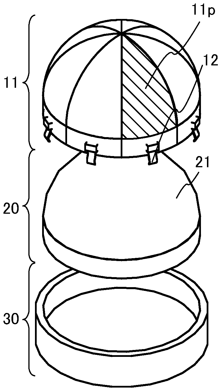
Die Anzeigevorrichtung 10A in
Die Anzeigevorrichtung 10A in
Das Befestigungsteil 20, auf dem die Vielzahl von Anzeigefeldern 11p befestigt wird, weist die gekrümmte Oberfläche 21 entlang der aus der Vielzahl von aneinandergebundenen Anzeigefeldern 11p gebildeten abwickelbaren Fläche auf. Wenn als Material des Befestigungsteils 20 ein Kunststoff, wie z. B. faserverstärkter Kunststoff (fiber-reinforced plastic, FRP), verwendet wird, kann eine gekrümmte Oberfläche mit einem leichteren Gewicht und einem ansprechenden Design erhalten werden. Als Befestigungsteil 20 kann ein Kunststoffsubstrat aus Polyimid (PI), Aramid, Polyethylenterephthalat (PET), Polyethersulfon (PES), Polyethylennaphthalat (PEN), Polycarbonat (PC), Nylon, Polyetheretherketon (PEEK), Polysulfon (PSF), Polyetherimid (PEI), Polyarylat (PAR), Polybutylenterephthalat (PBT), einem Silikonharz oder dergleichen verwendet werden. Des Weiteren weist die gekrümmte Oberfläche 21 bevorzugt eine hohe Stoßbeständigkeit auf, um eine Verformung des Anzeigefeldes 11p bei Berührung dieses zu verhindern.The fixing
In dem Gehäuse 30 wird ein Nichtanzeigeabschnitt des Anzeigefeldes 11, wie z. B. die FPC 12, aufgenommen, wobei die Vielzahl von Anzeigefeldern 11p entlang der gekrümmten Oberfläche 21 des Befestigungsteils 20 befestigt wird. Mit dieser Konfiguration kann die Anzeigevorrichtung eine Anzeigefläche mit einer gekrümmten Oberfläche aufweisen. In einem Hohlraum des Gehäuses 30 kann beispielsweise ein Airbag oder dergleichen aufgenommen werden.In the
Es sei angemerkt, dass, obwohl in
Es sei angemerkt, dass die Vielzahl von Anzeigefeldern 11p vorzugsweise voneinander getrennt sind. Mit dieser Konfiguration kann in dem Fall, in dem die Vielzahl von Anzeigefeldern 11p in Kombination miteinander eine hemisphärische Oberfläche bildet, eine Spannung an einem Verbindungsabschnitt zwischen den Anzeigefeldern 11p abgemildert werden.It should be noted that the plurality of
An dem Anzeigeabschnitt 14, an dem das Pixel 16 bereitgestellt wird, werden eine Anzeigeeinrichtung, wie z. B. eine Licht emittierende Einrichtung, und eine Pixelschaltung zum Steuern der Anzeige mittels der Anzeigeeinrichtung bereitgestellt. Der Nichtanzeigeabschnitt 15 ist derart angeordnet, um den Anzeigeabschnitt 14 zu umgeben, und mit der FPC 12 und der Source-Treiberschaltung 13 bereitgestellt.At the
Die Anzeigeeinrichtung und die Pixelschaltung, die in dem Anzeigeabschnitt 14 bereitgestellt werden, werden über dem Substrat bereitgestellt. Das Substrat, über dem die Anzeigeeinrichtung und die Pixelschaltung bereitgestellt werden, ist nicht rechteckig und weist eine Flexibilität auf. In dem Fall, in dem die hemisphärische Anzeigefläche in
Beispiele für Materialien eines derartigen Substrats umfassen Polyesterharze, wie z. B. PET und PEN, ein Polyacrylnitrilharz, ein Acrylharz, ein Polyimidharz, ein Polymethylmethacrylatharz, ein PC-Harz, ein PES-Harz, Polyamidharze (wie z. B. Nylon und Aramid), ein Polysiloxanharz, ein Cycloolefinharz, ein Polystyrolharz, ein Polyamidimidharz, ein Polyurethanharz, ein Polyvinylchloridharz, ein Polyvinylidenchloridharz, ein Polypropylenharz, ein PTFE-Harz und ein ABS-Harz. Im Besonderen wird ein Material bevorzugt, dessen Wärmeausdehnungskoeffizient niedrig ist, und beispielsweise kann ein Polyamidimidharz, ein Polyimidharz, ein Polyamidharz, PET oder dergleichen vorteilhaft verwendet werden. Des Weiteren kann auch ein Substrat, in dem eine Glasfaser mit einem organischen Harz imprägniert ist, oder ein Substrat verwendet werden, dessen Wärmeausdehnungskoeffizient verringert wird, indem einem organischen Harz ein anorganischer Füllstoff beigemischt wird. Diese Materialien des Substrats werden bevorzugt, da im Unterschied zu Glas oder dergleichen die Gefahr des Zerstreuens der Scherben beim Stoß verringert wird.Examples of materials of such a substrate include polyester resins such as: B. PET and PEN, a polyacrylonitrile resin, an acrylic resin, a polyimide resin, a polymethyl methacrylate resin, a PC resin, a PES resin, polyamide resins (such as nylon and aramid), a polysiloxane resin, a cycloolefin resin, a polystyrene resin polyamideimide resin, a polyurethane resin, a polyvinyl chloride resin, a polyvinylidene chloride resin, a polypropylene resin, a PTFE resin and an ABS resin. In particular, a material whose coefficient of thermal expansion is low is preferred, and, for example, a polyamideimide resin, a polyimide resin, a polyamide resin, PET or the like can be advantageously used. Furthermore, a substrate in which a glass fiber is impregnated with an organic resin or a substrate whose coefficient of thermal expansion is reduced by mixing an inorganic filler with an organic resin can also be used. These materials of the substrate are preferred because, unlike glass or the like, the risk of the shards scattering upon impact is reduced.
Das flexible Substrat kann eine mehrschichtige Struktur aufweisen, bei der mindestens eine von einer Hartschicht (wie z. B. einer Siliziumnitridschicht), durch die eine Oberfläche der Vorrichtung vor Schäden geschützt wird, einer Schicht, die Druck verteilen kann (wie z. B. einer Aramidharzschicht), und dergleichen über einer Schicht aus einem beliebigen der vorstehend genannten Materialien angeordnet ist.The flexible substrate may have a multilayer structure, in which at least one of a hard layer (such as a silicon nitride layer) that protects a surface of the device from damage, a layer that can distribute pressure (such as an aramid resin layer), and the like is disposed over a layer of any of the above-mentioned materials.
Ein flexibles Substrat kann zu einer nicht rechteckigen Form verarbeitet oder geschnitten werden. Es sei angemerkt, dass die Pixelschaltung und die Anzeigeeinrichtung durch ein Verfahren, in dem sie direkt auf dem flexiblen Substrat ausgebildet werden, oder ein Verfahren ausgebildet werden können, in dem ein Transistor, eine Licht emittierende Einrichtung und dergleichen auf einem Glassubstrat oder dergleichen ausgebildet werden und danach von dem Glassubstrat abgelöst werden und unter Verwendung einer Klebeschicht an das flexible Substrat verbunden werden. Es gibt verschiedene Arten von Ablöseverfahren oder Übertragungsverfahren und keine besondere Beschränkung; dabei kann eine bekannte Technik angemessen zum Einsatz kommen. Als Verbindungsschicht können verschiedene härtende Klebstoffe verwendet werden, wie beispielsweise ein lichthärtender Klebstoff, wie z. B. ein UV-härtender Klebstoff, ein reaktiv härtender Klebstoff, ein wärmehärtender Klebstoff und ein anaerober Klebstoff. Eine Klebefolie oder dergleichen kann auch verwendet werden.A flexible substrate can be processed or cut into a non-rectangular shape. It should be noted that the pixel circuit and the display device can be formed by a method in which it is directly formed on the flexible substrate, or a method in which a transistor, a light emitting device and the like are formed on a glass substrate or the like and thereafter peeled off from the glass substrate and bonded to the flexible substrate using an adhesive layer. There are various types of redemption procedures or transfer procedures and no particular limitation; A known technique can be used appropriately. Various curing adhesives can be used as the connecting layer, such as a light-curing adhesive, such as. B. a UV-curing adhesive, a reactive-curing adhesive, a thermosetting adhesive and an anaerobic adhesive. An adhesive film or the like can also be used.
Die Anzeigeeinrichtung und die Pixelschaltung, die in dem Anzeigeabschnitt 14 bereitgestellt werden, werden in einer Matrix angeordnet. Bei dieser Ausführungsform wird als Anzeigeeinrichtung ein organisches EL-Element verwendet, das eine Licht emittierende Einrichtung ist.The display device and the pixel circuit provided in the
Als Farbumwandlungselement (Wellenlängeumwandlungselement) des organischen EL-Elements kann ein Quantenpunktmaterial verwendet werden. Bei einem Quantenpunkt handelt es sich um einen Halbleiter-Nanokristall mit einem Durchmesser von mehreren Nanometern bis mehreren zehn Nanometern, und er enthält ungefähr 1 × 10³ bis 1 × 10⁶ Atome. Ein Quantenpunkt schließt ein Elektron, ein Loch oder ein Exziton ein, was zu diskreten Energiezuständen und einer von der Größe eines Quantenpunkts abhängigen Energieverschiebung führt. Dies bedeutet, dass Quantenpunkten, die aus der gleichen Substanz bestehen, in Abhängigkeit von ihren Größen Licht mit unterschiedlichen Emissionswellenlängen emittieren; somit können Emissionswellenlängen durch Änderung der Größen von Quantenpunkten leicht angepasst werden.A quantum dot material can be used as the color conversion element (wavelength conversion element) of the organic EL element. A quantum dot is a semiconductor nanocrystal with a diameter of several nanometers to tens of nanometers and contains approximately 1 × 10 3 to 1 × 10 6 atoms. A quantum dot encloses an electron, a hole, or an exciton, resulting in discrete energy states and an energy shift dependent on the size of a quantum dot. This means that quantum dots, which are made of the same substance, emit light with different emission wavelengths depending on their sizes; thus, emission wavelengths can be easily adjusted by changing the sizes of quantum dots.
Des Weiteren kann der Anzeigeabschnitt 14 eine Funktion des Touchscreens aufweisen. Er kann derart hergestellt werden, dass er durch Berührung mit einer Hand, Haltung einer Hand darüber oder die Gesten eines Benutzers bedient werden kann.Furthermore, the
Es sei angemerkt, dass in dem Fall, in dem Licht emittierende Einrichtungen, wie z. B. organische EL-Elemente, eine feine Metallmasken- (FMM-) Struktur aufweisen, die Einrichtungen innerhalb derselben Oberfläche nur schwer mit verschiedenen Definitionen ausgebildet werden können. Hier wird im Folgenden die FMM-Struktur beschrieben.It should be noted that in the case where light emitting devices such as B. organic EL elements have a fine metal mask (FMM) structure, the devices within the same surface are difficult to form with different definitions. The FMM structure is described below.
Zur Herstellung der FMM-Struktur wird bei der EL-Verdampfung eine Maske aus Metall (auch als FMM bezeichnet), an der ein Öffnungsabschnitt derart bereitgestellt ist, dass EL-Materialien in dem erwünschten Bereich verdampft werden, dem Substrat zugewandt gesetzt. Danach wird eine EL-Verdampfung über die FMM durchgeführt, so dass EL-Materialien in dem erwünschten Bereich verdampft werden. Wenn die Größe des Substrats bei der EL-Verdampfung zunimmt, nehmen auch die Größe und das Gewicht der FMM zu. Des Weiteren wird die FMM in einigen Fällen verformt, da der FMM bei der EL-Verdampfung die Wärme oder dergleichen zugeführt wird. Alternativ kann eine Verdampfung durchgeführt werden, bei der der FMM eine gewisse Spannung bei der EL-Verdampfung gegeben wird; daher handelt es sich bei dem Gewicht und der Festigkeit der FMM um wichtige Parameter.To produce the FMM structure, in EL evaporation, a mask made of metal (also referred to as FMM), on which an opening portion is provided such that EL materials are evaporated in the desired area, is placed facing the substrate. After that, EL evaporation is performed via the FMM so that EL materials are evaporated in the desired area. As the size of the substrate increases in EL evaporation, the size and weight of the FMM also increase. Furthermore, in some cases, the FMM is deformed because the heat or the like is supplied to the FMM in the EL evaporation. Alternatively, evaporation can be performed in which the FMM is given a certain voltage during EL evaporation; therefore, the weight and strength of the FMM are important parameters.
Deshalb muss in dem Fall, in dem die Definition innerhalb der Oberfläche des Anzeigefeldes 11p unter Verwendung der FMM geändert wird, die Auslegung der FMM geändert werden. Jedoch müssen in dem Fall, in dem die Auslegung der FMM geändert wird, auch die Verformung der FMM und dergleichen berücksichtigt werden; daher ist es sehr schwierig, die Definition innerhalb der Oberfläche des Anzeigefeldes zu ändern. Im Gegensatz dazu ermöglicht das Anzeigefeld einer Ausführungsform der vorliegenden Erfindung eine ausgezeichnete Wirkung zur Erleichterung der Änderung der Definition innerhalb der Oberfläche des Anzeigefeldes, da es unter Verwendung einer Struktur ohne Metallmaske (metal maskless structure, MML-Struktur) hergestellt wird. Das heißt, dass das Anzeigefeld einer Ausführungsform der vorliegenden Erfindung (beispielsweise nicht rechteckiges, flexibles Anzeigefeld) und die MML-Struktur zueinander gut passen. Mit anderen Worten: Das flexible Anzeigefeld und die MML-Struktur weisen eine hohe Affinität zueinander auf.Therefore, in the case where the definition within the surface of the
Es sei angemerkt, dass in dieser Beschreibung und dergleichen eine unter Verwendung einer Metallmaske oder einer FMM (einer feinen Metallmaske, einer Metallmaske mit hoher Feinheit) ausgebildete Einrichtung als Einrichtung mit einer MM-(Metallmaske-) Struktur bezeichnet werden kann. In dieser Beschreibung und dergleichen kann eine ohne Verwendung einer Metallmaske oder einer FMM ausgebildete Einrichtung als Einrichtung mit einer MML- (metallmaskenlosen) Struktur bezeichnet werden.It should be noted that in this specification and the like, a device formed using a metal mask or an FMM (a fine metal mask, a high fineness metal mask) may be referred to as a device having an MM (metal mask) structure. In this specification and the like, a device formed without using a metal mask or an FMM may be referred to as a device having an MML (metal maskless) structure.
Der Nichtanzeigeabschnitt 15 ist ein Bereich, in dem das Pixel 16 nicht bereitgestellt wird, und in der Position, die sich mit dem Nichtanzeigeabschnitt 15 überlappt, wird die Source-Treiberschaltung bereitgestellt. Die Source-Treiberschaltung 13 wird in dem Nichtbiegebereich 13AR des Nichtanzeigeabschnitts 15 bereitgestellt. Die Gate-Treiberschaltung 17 kann in der Position bereitgestellt werden, die sich mit dem Anzeigeabschnitt 14 überlappt, indem sie einen Transistor umfasst, der durch den gleichen Prozess wie denjenigen für die Pixelschaltung in dem Pixel 16 hergestellt wird. Ein Konfigurationsbeispiel der Gate-Treiberschaltung 17 wird nachstehend beschrieben. Wenn die Gate-Treiberschaltung 17 einen durch den gleichen Prozess wie denjenigen für die Pixelschaltung hergestellten Transistor umfasst, kann die Gate-Treiberschaltung 17 selbst in dem Biegebereich 17AR weniger wahrscheinlich gebrochen werden. Ferner kann eine Anzeigevorrichtung mit einem ansprechenden Design erhalten werden, da, wenn die Gate-Treiberschaltung 17 in dem Anzeigeabschnitt 14 angeordnet werden kann, selbst bei dem nicht rechteckigen Anzeigeabschnitt die Pixel betrieben werden können.The
Es sei angemerkt, dass in dieser Beschreibung und dergleichen die Beschreibung erfolgt, in der der Einfachheit halber eine kleinste Einheit, die in einem „Pixel“ unabhängig arbeitet, als „Subpixel“ definiert wird, und dass das „Pixel“ durch „Bereich“ und das „Subpixel“ durch „Pixel“ ersetzt werden können.It should be noted that in this description and the like, the description is made in which, for convenience, a smallest unit operating independently in a "pixel" is defined as a "subpixel", and the "pixel" is replaced by "area" and the “subpixel” can be replaced by “pixel”.
Bei der Anzeigevorrichtung dieser Ausführungsform kann ein Pixel 16 mehrere Arten von Subpixeln mit Licht unterschiedlicher Farben emittierenden Einrichtungen aufweisen. Beispielsweise kann das in
Das Subpixel 16R weist eine rotes Licht emittierende Einrichtung auf. Das Subpixel 16G weist eine grünes Licht emittierende Einrichtung auf. Das Subpixel 16B weist eine blaues Licht emittierende Einrichtung auf.The
Die Anordnung von Subpixeln ist nicht besonders beschränkt, und verschiedene Verfahren können verwendet werden. Als Anordnung von Subpixeln können beispielsweise eine Streifen-Anordnung, eine S-Streifen-Anordnung, eine Matrix-Anordnung, eine Delta-Anordnung, eine Bayer-Anordnung und eine PenTile-Anordnung angegeben werden.The arrangement of subpixels is not particularly limited, and various methods can be used. As an arrangement of subpixels, for example, a stripe arrangement, an S-stripe arrangement, a matrix arrangement, a delta arrangement, a Bayer arrangement and a PenTile arrangement can be specified.
Des Weiteren können Oberseiten der Subpixel beispielsweise eine dreieckige Form, eine viereckige Form (einschließlich einer rechteckigen Form und einer quadratischen Form), eine polygonale Form, wie z. B. eine fünfeckige Form, eine polygonale Form mit abgerundeten Ecken, eine elliptische Form oder eine Kreisform aufweisen. Die Oberseitenform eines Subpixels hier entspricht einer Oberseitenform eines Licht emittierenden Bereichs einer Licht emittierenden Einrichtung.Further, tops of the subpixels may, for example, have a triangular shape, a quadrangular shape (including a rectangular shape and a square shape), a polygonal shape such as: B. have a pentagonal shape, a polygonal shape with rounded corners, an elliptical shape or a circular shape. The top shape of a subpixel here corresponds to a top shape of a light-emitting region of a light-emitting device.
Darüber hinaus kann bei der in dem Pixel eine Licht emittierende Einrichtung und eine Licht empfangende Einrichtung umfassenden Anzeigevorrichtung beispielsweise das Pixel 16PIX in
Das Subpixel 16PS umfasst eine Licht empfangende Einrichtung. Obwohl die Wellenlänge von durch Subpixel 16PS erfasstem Licht nicht besonders beschränkt ist, weist die Licht empfangende Einrichtung des Subpixels 16PS vorzugsweise die Empfindlichkeit gegenüber Licht auf, das von der Licht emittierenden Einrichtung des Subpixels R, des Subpixels G oder des Subpixels B emittiert wird.The subpixel 16PS includes a light receiving device. Although the wavelength of light detected by subpixel 16PS is not particularly limited, the light receiving device of subpixel 16PS preferably has the sensitivity to light emitted from the light emitting device of subpixel R, subpixel G, or subpixel B.
Die Licht empfangende Fläche des Subpixels 16PS kann kleiner sein als Licht emittierende Fläche der anderen Subpixel. Durch Verwendung des Subpixels 16PS ist daher eine Abbildung mit hoher Auflösung oder hoher Bildschärfe möglich. Beispielsweise ist durch Verwendung des Subpixels 16PS eine Abbildung für eine persönliche Authentifizierung unter Verwendung eines Fingerabdrucks, eines Handflächenabdrucks, der Iris, der Form eines Blutgefäßes (einschließlich der Form einer Vene und der Form einer Arterie), eines Gesichts oder dergleichen möglich.The light receiving area of the subpixel 16PS may be smaller than the light emitting area of the other subpixels. By using the subpixel 16PS, imaging with high resolution or high image sharpness is possible. For example, by using the subpixel 16PS, an image for personal authentication using a fingerprint, a palm print, the iris, the shape of a blood vessel (including the shape of a vein and the shape of an artery), a face, or the like is possible.
Außerdem kann das Subpixel 16PS in einem Berührungssensor (auch als direkter Berührungssensor bezeichnet), einem Beinahe-Berührungssensor (auch als Schwebesensor, Schwebe-Berührungssensor, kontaktloser Sensor oder berührungsloser Sensor bezeichnet) oder dergleichen verwendet werden. Beispielsweise erfasst das Subpixel 16PS vorzugsweise Infrarotlicht. Daher kann eine Berührung auch in einer dunklen Umgebung erfasst werden.In addition, the subpixel 16PS can be used in a touch sensor (also called a direct touch sensor), a near-touch sensor (also called a hover sensor, floating touch sensor, contactless sensor or non-contact sensor) or the like. For example, the subpixel 16PS preferably detects infrared light. Therefore A touch can also be detected in a dark environment.
Hier kann der Berührungssensor oder der Beinahe-Berührungssensor eine Annäherung oder einen Kontakt eines Objekts (z. B. eines Fingers, einer Hand oder eines Stifts) erkennen. Der Berührungssensor kann das Objekt erkennen, wenn die Anzeigevorrichtung und das Objekt in direktem Kontakt miteinander kommen. Des Weiteren kann der Beinahe-Berührungssensor selbst dann, wenn das Objekt nicht in Kontakt mit der Anzeigevorrichtung ist, das Objekt erkennen. Beispielsweise kann die Anzeigevorrichtung vorzugsweise das Objekt erkennen, wenn der Abstand zwischen der Anzeigevorrichtung und dem Objekt größer als oder gleich 0,1 mm und kleiner als oder gleich 300 mm, bevorzugt größer als oder gleich 3 mm und kleiner als oder gleich 50 mm beträgt. Mit dieser Struktur kann die Anzeigevorrichtung gesteuert werden, ohne dass dabei das Objekt in direktem Kontakt mit der Anzeigevorrichtung kommt; mit anderen Worten: Die Anzeigevorrichtung kann kontaktlos (berührungslos) gesteuert werden. Mit der vorstehenden Struktur kann die Anzeigevorrichtung mit einer verringerten Gefahr, schmutzig oder beschädigt zu werden, oder ohne direkten Kontakt zwischen dem Objekt und einem an der Anzeigevorrichtung haftenden Schmutz (z. B. Staub, Bakterien oder einem Virus) gesteuert werden.Here, the touch sensor or the near-touch sensor can detect an approach or contact of an object (e.g. a finger, a hand or a pen). The touch sensor can detect the object when the display device and the object come into direct contact with each other. Furthermore, even if the object is not in contact with the display device, the near-touch sensor can detect the object. For example, the display device can preferably detect the object if the distance between the display device and the object is greater than or equal to 0.1 mm and less than or equal to 300 mm, preferably greater than or equal to 3 mm and less than or equal to 50 mm. With this structure, the display device can be controlled without the object coming into direct contact with the display device; in other words: the display device can be controlled in a contactless (non-contact) manner. With the above structure, the display device can be controlled with a reduced risk of becoming dirty or damaged, or without direct contact between the object and a dirt (e.g., dust, bacteria, or a virus) adhering to the display device.
Es sei angemerkt, dass zur Abbildung mit hoher Definition jedes Pixel der Anzeigevorrichtung vorzugsweise mit dem Subpixel 16PS versehen ist. Währenddessen wird in dem Fall, in dem das Subpixel 16PS in einem Berührungssensor, einem Beinahe-Berührungssensor oder dergleichen verwendet wird, eine hohe Genauigkeit im Vergleich zu dem Fall der Abbildung eines Bildes eines Fingerabdrucks oder dergleichen nicht benötigt; folglich wird das Subpixel 16PS in einigen Subpixeln in der Anzeigevorrichtung bereitgestellt. Wenn die Subpixel 16PS der Anzeigevorrichtung weniger sind als die Subpixel 16R und dergleichen, wird eine Erkennung mit höherer Geschwindigkeit ermöglicht.It should be noted that for high definition imaging, each pixel of the display device is preferably provided with the subpixel 16PS. Meanwhile, in the case where the subpixel 16PS is used in a touch sensor, a near-touch sensor or the like, high accuracy is not required compared to the case of imaging an image of a fingerprint or the like; hence, the subpixel 16PS is provided in some subpixels in the display device. When the subpixels 16PS of the display device are fewer than the
Die Pixelschaltung 16el in
Ein Gate des Transistors M11 ist elektrisch mit einer Leitung GL verbunden, sein einer Anschluss von Source und Drain ist elektrisch mit einer Leitung SL verbunden, und sein anderer Anschluss von Source und Drain ist elektrisch mit einer Elektrode des Kondensators C11 und einem Gate des Transistors M12 verbunden. Ein Anschluss von Source oder Drain des Transistors M12 ist elektrisch mit einer Leitung EAL verbunden, und der andere ist elektrisch mit einer Anode der Licht emittierenden Einrichtung EL und der anderen Elektrode des Kondensators C11 verbunden. Eine Kathode der Licht emittierenden Einrichtung EL ist elektrisch mit einer Leitung ACL verbunden.A gate of the transistor M11 is electrically connected to a line GL, one of its source and drain is electrically connected to a line SL, and its other source and drain is electrically connected to an electrode of the capacitor C11 and a gate of the transistor M12 tied together. One terminal of the source or drain of the transistor M12 is electrically connected to a line EAL, and the other is electrically connected to an anode of the light-emitting device EL and the other electrode of the capacitor C11. A cathode of the light-emitting device EL is electrically connected to a line ACL.
Der Leitung EAL und der Leitung ACL wird jeweils ein konstantes Potential zugeführt. Die Anodenseite der Licht emittierenden Einrichtung EL kann auf ein hohes Potential eingestellt werden, während die Kathodenseite auf ein niedrigeres Potential als dasjenige der Anodenseite eingestellt werden kann. Der Transistor M11 wird durch ein Signal gesteuert, das der Leitung GL zugeführt wird, und dient als Auswahltransistor zum Steuern eines Auswahlzustands der Pixelschaltung 16el. Der Transistor M12 dient als Treibertransistor zum Steuern eines durch die Licht emittierende Einrichtung EL fließenden Stroms entsprechend dem seinem Gate zugeführten Potential. Es sei angemerkt, dass, obwohl zwei Transistoren als Transistor in der Pixelschaltung 16el beschrieben worden sind, die Pixelschaltung 16el drei oder mehr Transistoren aufweisen kann.The EAL line and the ACL line are each supplied with a constant potential. The anode side of the light-emitting device EL can be set to a high potential, while the cathode side can be set to a lower potential than that of the anode side. The transistor M11 is controlled by a signal supplied to the line GL and serves as a selection transistor for controlling a selection state of the pixel circuit 16el. The transistor M12 serves as a driving transistor for controlling a current flowing through the light-emitting device EL in accordance with the potential supplied to its gate. It should be noted that although two transistors have been described as a transistor in the pixel circuit 16el, the pixel circuit 16el may include three or more transistors.
Eine Pixelschaltung 16ps in
Eine Anode der Licht empfangenden Einrichtung PS ist elektrisch mit einer Leitung ACL verbunden, und ihre Kathode ist elektrisch mit einem Anschluss von Source und Drain des Transistors M15 verbunden. Das Gate des Transistors M15 ist elektrisch mit einer Leitung TX verbunden, und sein anderer Anschluss von Source und Drain ist elektrisch mit einer Elektrode des Kondensators C21, einem Anschluss von Source und Drain des Transistors M16 und einem Gate des Transistors M17 verbunden. Ein Gate des Transistors M16 ist elektrisch mit einer Leitung RS verbunden, und der andere Anschluss von Source und Drain des Transistors M16 ist elektrisch mit einer Leitung V11 verbunden. Ein Anschluss von Source und Drain des Transistors M17 ist elektrisch mit einer Leitung V13 verbunden, und sein anderer Anschluss von Source und Drain ist elektrisch mit einem Anschluss von Source und Drain des Transistors M18 verbunden. Das Gate des Transistors M18 ist elektrisch mit einer Leitung SE verbunden, und sein anderer Anschluss von Source und Drain ist elektrisch mit einer Leitung WX verbunden. Die andere Elektrode des Kondensators C21 ist elektrisch mit einer Leitung V12 verbunden.An anode of the light receiving device PS is electrically connected to a line ACL, and its cathode is electrically connected to a source and drain of the transistor M15. The gate of the transistor M15 is electrically connected to a line TX, and its other source and drain terminal is electrically connected to an electrode of the capacitor C21, a source and drain terminal of the transistor M16, and a gate of the transistor M17. A gate of the transistor M16 is electrically connected to a line RS, and the other terminal of the source and drain of the transistor M16 is electrically connected to a line V11. A connection of the source and drain of the transistor M17 is electrically connected to a line V13, and its other source and drain terminal is electrically connected to a source and drain terminal of the transistor M18. The transistor M18 has its gate electrically connected to a line SE, and its other source and drain terminals electrically connected to a line WX. The other electrode of the capacitor C21 is electrically connected to a line V12.
Es sei angemerkt, dass in dem Fall, in dem die Licht empfangende Einrichtung PS bereitgestellt wird, die Bereitstellung einer Vielzahl der Gate-Treiberschaltungen 17 in
Der Leitung V11, der Leitung V12 und der Leitung V13 wird jeweils ein konstantes Potential zugeführt. Wenn die Licht empfangende Vorrichtung PS mit einer Vorwärtsvorspannung betrieben wird, wird der Leitung V11 ein niedrigeres Potential als das Potential der Leitung ACL zugeführt. Der Transistor M16 wird durch ein der Leitung RS zugeführtes Signal gesteuert und weist eine Funktion zum Zurücksetzen des Potentials eines mit dem Gate des Transistors M17 verbundenen Knotens auf das der Leitung V11 zugeführte Potential auf. Der Transistor M15 wird durch ein Signal, das der Leitung TX zugeführt wird, gesteuert und funktioniert, um den Zeitpunkt, zu dem sich das Potential des vorstehenden Knotens entsprechend einem durch die Licht empfangende Vorrichtung PS fließenden Strom verändert, zu steuern. Der Transistor M17 dient als Verstärkertransistor, der eine Ausgabe entsprechend dem Potential des Knotens durchführt. Der Transistor M18 wird durch ein Signal gesteuert, das der Leitung SE zugeführt wird, und dient als Auswahltransistor zum Lesen der Ausgabe, die dem Potential des vorstehenden Knotens entspricht, durch eine externe Schaltung, die mit der Leitung WX verbunden ist.A constant potential is each supplied to line V11, line V12 and line V13. When the light receiving device PS is operated with a forward bias voltage, the line V11 is supplied with a lower potential than the potential of the line ACL. The transistor M16 is controlled by a signal supplied to the line RS and has a function of resetting the potential of a node connected to the gate of the transistor M17 to the potential supplied to the line V11. The transistor M15 is controlled by a signal supplied to the line TX and functions to control the timing at which the potential of the protruding node changes in accordance with a current flowing through the light receiving device PS. Transistor M17 serves as an amplifier transistor that performs output according to the potential of the node. The transistor M18 is controlled by a signal supplied to the line SE and serves as a selection transistor for reading the output corresponding to the potential of the above node through an external circuit connected to the line WX.
Es sei angemerkt, dass, obwohl n-Kanal-Transistoren als Transistoren in
Die Transistoren der Pixelschaltung 16el und die Transistoren der Pixelschaltung 16ps werden vorzugsweise über demselben Substrat nebeneinander ausgebildet. Insbesondere ist eine Struktur bevorzugt, bei der die Transistoren der Pixelschaltung 16el und die Transistoren der Pixelschaltung 16ps in einem Bereich periodisch angeordnet sind.The transistors of the pixel circuit 16el and the transistors of the pixel circuit 16ps are preferably formed side by side over the same substrate. In particular, a structure in which the transistors of the pixel circuit 16el and the transistors of the pixel circuit 16ps are periodically arranged in an area is preferred.
Vorzugsweise werden eine oder mehrere Schichten mit einem Transistor und/oder einem Kondensator in einer mit der Licht empfangenden Einrichtung PS oder der Licht emittierenden Einrichtung EL überlappenden Position bereitgestellt. Daher kann die von jeder Pixelschaltung eingenommene effektive Fläche verringert werden, und ein Licht empfangender Abschnitt oder ein Anzeigeabschnitt mit hoher Definition kann erhalten werden.Preferably, one or more layers with a transistor and/or a capacitor are provided in a position overlapping with the light-receiving device PS or the light-emitting device EL. Therefore, the effective area occupied by each pixel circuit can be reduced, and a light receiving section or a high definition display section can be obtained.
Hierbei kommt vorzugsweise bei den Transistoren M11 und M12 in der Pixelschaltung 16el sowie den Transistoren M15 bis M18 in der Pixelschaltung 16ps jeweils ein Transistor zum Einsatz, der in einer Halbleiterschicht, in der ein Kanal gebildet wird, ein Metalloxid (einen Oxidhalbleiter) enthält.In this case, the transistors M11 and M12 in the pixel circuit 16el and the transistors M15 to M18 in the pixel circuit 16ps preferably each use a transistor which contains a metal oxide (an oxide semiconductor) in a semiconductor layer in which a channel is formed.
Ein Transistor enthaltend ein Metalloxid mit einer größeren Bandlücke und einer niedrigeren Ladungsträgerdichte als Silizium ermöglicht einen sehr niedrigen Sperrstrom. Daher ermöglicht ein derartiger geringer Sperrstrom, dass Ladungen, die in einem in Reihe mit dem Transistor geschalteten Kondensator akkumuliert sind, für eine lange Zeit gehalten werden. Daher wird insbesondere jeweils als Transistor M11, Transistor M15 und Transistor M16, welche mit dem Kondensator C11 bzw. dem Kondensator C21 in Reihe geschaltet sind, vorzugsweise ein Transistor verwendet, bei dem ein Oxidhalbleiter zum Einsatz kommt. Wenn ebenfalls ein Transistor, bei dem ein Oxidhalbleiter zum Einsatz kommt, jeweils als weitere Transistoren verwendet wird, können die Herstellungskosten verringert werden. Jedoch ist eine Ausführungsform der vorliegenden Erfindung nicht darauf beschränkt. Ein Transistor, der in einer Halbleiterschicht Silizium verwendet wird (nachstehend auch als Si-Transistor bezeichnet), kann auch verwendet werden.A transistor containing a metal oxide with a larger band gap and a lower charge carrier density than silicon enables a very low reverse current. Therefore, such a low reverse current allows charges accumulated in a capacitor connected in series with the transistor to be held for a long time. Therefore, a transistor in which an oxide semiconductor is used is preferably used as the transistor M11, transistor M15 and transistor M16, which are connected in series with the capacitor C11 and the capacitor C21, respectively. Also, if a transistor using an oxide semiconductor is used as other transistors, the manufacturing cost can be reduced. However, an embodiment of the present invention is not limited to this. A transistor used in a semiconductor layer of silicon (hereinafter also referred to as Si transistor) can also be used.
Der Sperrstrom pro Mikrometer der Kanalbreite des OS-Transistors bei Raumtemperatur kann niedriger als oder gleich 1 aA (1 × 10-18 A), niedriger als oder gleich 1 zA (1 × 10-21 A) oder niedriger als oder gleich 1 yA (1 × 10-24 A) sein. Es sei angemerkt, dass der Sperrstrom pro Mikrometer der Kanalbreite eines Si-Transistors bei Raumtemperatur höher als oder gleich 1 fA (1 × 10-15 A) und niedriger als oder gleich 1 pA (1 × 10-12 A) ist. Mit anderen Worten: Der Sperrstrom des OS-Transistors ist um ungefähr zehn Zehnerpotenzen niedriger als derjenige des Si-Transistors.The reverse current per micrometer of the channel width of the OS transistor at room temperature can be lower than or equal to 1 aA (1 × 10 -18 A), lower than or equal to 1 zA (1 × 10 -21 A), or lower than or equal to 1 yA ( 1 × 10 -24 A). Note that the reverse current per micrometer of channel width of a Si transistor at room temperature is higher than or equal to 1 fA (1 × 10 -15 A) and lower than or equal to 1 pA (1 × 10 -12 A). In other words, the reverse current of the OS transistor is approximately ten orders of magnitude lower than that of the Si transistor.
Es sei angemerkt, dass die Anzeigevorrichtung einer Ausführungsform der vorliegenden Erfindung eine Struktur aufweist, die den OS-Transistor und das Licht emittierende Element mit einer metallmaskenlosen (metal maskless, MML-) Struktur umfasst. Mit dieser Struktur können der Leckstrom, der durch den Transistor fließen könnte, und der Leckstrom, der zwischen benachbarten Licht emittierenden Elementen fließen könnte (auch als lateraler Leckstrom, seitlicher Leckstrom oder dergleichen bezeichnet) sehr niedrig werden. Mit dieser Struktur kann ein Betrachter eine oder mehrere der Knackigkeit eines Bildes, der Schärfe eines Bildes und eines hohen Kontrastverhältnisses in einem Bild wahrnehmen, das auf der Anzeigeeinrichtung angezeigt wird. Wenn der Leckstrom, der durch den Transistor fließen könnte, und der laterale Leckstrom, der zwischen Licht emittierenden Elementen fließen könnte, sehr niedrig sind, kann eine Anzeige mit geringem Lichtaustritt bei der schwarzen Anzeige (eine derartige Anzeige wird auch als tief schwarze Anzeige bezeichnet) erzielt werden.It is noted that the display device of an embodiment of the present invention has a structure including the OS transistor and the light-emitting element with a metal maskless (MML) structure. With this structure, the leakage current that could flow through the transistor and the leakage current that could flow between adjacent light-emitting elements (also called lateral leakage current, lateral leakage current, or the like) can become very low. With this structure, a viewer can experience one or more of the crispness of an image, the sharpness of an image and a perceive high contrast ratio in an image displayed on the display device. If the leakage current that could flow through the transistor and the lateral leakage current that could flow between light-emitting elements are very low, a display with low light leakage in the black display (such a display is also called a deep black display) be achieved.
Um die Leuchtdichte der Licht emittierenden Einrichtung, die in der Pixelschaltung enthalten ist, zu erhöhen, muss die Menge an Strom, der durch die Licht emittierende Vorrichtung geleitet wird, erhöht werden. Um die Strommenge zu erhöhen, muss ferner die Source-Drain-Spannung eines Treibertransistors, der in der Pixelschaltung enthalten ist, erhöht werden. Ein OS-Transistor weist eine höhere Spannungsfestigkeit zwischen einer Source und einem Drain auf als ein Si-Transistor; somit kann eine hohe Spannung zwischen der Source und dem Drain des OS-Transistors angelegt werden. Dementsprechend kann dann, wenn der Ansteuertransistor in der Pixelschaltung ein OS-Transistor ist, eine hohe Spannung zwischen der Source und dem Drain des OS-Transistors angelegt werden; dadurch kann die Menge an Strom, der in die Licht emittierende Einrichtung hineinfließt, vergrößert werden und die Emissionsleuchtdichte der Licht emittierenden Einrichtung kann erhöht werden.In order to increase the luminance of the light-emitting device included in the pixel circuit, the amount of current passed through the light-emitting device must be increased. Further, in order to increase the amount of current, the source-drain voltage of a driver transistor included in the pixel circuit must be increased. An OS transistor has a higher voltage strength between a source and a drain than a Si transistor; thus, a high voltage can be applied between the source and drain of the OS transistor. Accordingly, when the drive transistor in the pixel circuit is an OS transistor, a high voltage can be applied between the source and drain of the OS transistor; thereby, the amount of current flowing into the light-emitting device can be increased and the emission luminance of the light-emitting device can be increased.
Wenn Transistoren in einem Sättigungsbereich arbeiten, kann eine Änderung eines Source-Drain-Stroms bezüglich einer Änderung einer Gate-Source-Spannung in einem OS-Transistor kleiner sein als in einem Si-Transistor. Dementsprechend kann dann, wenn ein OS-Transistor als Treibertransistor in der Pixelschaltung verwendet wird, ein Strom, der zwischen der Source und dem Drain fließt, exakt gemäß einer Änderung der Gate-Source-Spannung eingestellt werden; somit kann die Menge an Strom, der durch die Licht emittierende Vorrichtung fließt, fein gesteuert werden. Daher kann die Emissionsleuchtdichte der Licht emittierenden Einrichtung fein gesteuert werden (die Anzahl der Graustufe der Pixelschaltung kann vermehrt werden).When transistors operate in a saturation region, a change in source-drain current with respect to a change in gate-source voltage may be smaller in an OS transistor than in a Si transistor. Accordingly, when an OS transistor is used as a driving transistor in the pixel circuit, a current flowing between the source and the drain can be accurately adjusted according to a change in the gate-source voltage; thus, the amount of current flowing through the light-emitting device can be finely controlled. Therefore, the emission luminance of the light-emitting device can be finely controlled (the number of gray levels of the pixel circuit can be increased).
Bezüglich der Sättigungseigenschaften eines Stroms, der in dem Fall fließt, in dem Transistoren in einem Sättigungsbereich arbeiten, kann selbst dann, wenn sich die Source-Drain-Spannung eines OS-Transistors allmählich erhöht, ein stabilerer konstanter Strom (Sättigungsstrom) durch den OS-Transistor geleitet werden als durch einen Si-Transistor. Daher kann unter Verwendung eines OS-Transistors als Treibertransistor ein stabiler konstanter Strom durch Licht emittierende Einrichtungen, die EL-Materialien enthalten, geleitet werden, selbst wenn beispielsweise die Strom-Spannung-Eigenschaften der Licht emittierenden Vorrichtungen variieren. Mit anderen Worten: Wenn der OS-Transistor in dem Sättigungsbereich arbeitet, ändert sich der Source-Drain-Strom kaum mit einer Erhöhung der Source-Drain-Spannung; somit kann die Leuchtdichte der Licht emittierenden Einrichtung stabil sein.Regarding the saturation characteristics of a current flowing in the case where transistors operate in a saturation region, even if the source-drain voltage of an OS transistor increases gradually, a more stable constant current (saturation current) can be provided by the OS Transistor are conducted than through a Si transistor. Therefore, by using an OS transistor as a driving transistor, a stable constant current can be passed through light-emitting devices containing EL materials even if, for example, the current-voltage characteristics of the light-emitting devices vary. In other words, when the OS transistor operates in the saturation region, the source-drain current hardly changes with an increase in the source-drain voltage; thus, the luminance of the light-emitting device can be stable.
Wie vorstehend beschrieben, ist es unter Verwendung eines OS-Transistors als Treibertransistor, der in der Pixelschaltung enthalten ist, möglich, „die Verhinderung des schwarzen Floating“, „die Erhöhung der Emissionsleuchtdichte“, „die Erhöhung der Graustufe“, „die Verhinderung der Variation in Licht emittierenden Einrichtungen“ und dergleichen zu erzielen. Deshalb kann die die Pixelschaltung enthaltende Anzeigevorrichtung ein klares und ruckelfreies Bild anzeigen; infolgedessen können die Knackigkeit eines Bildes und/oder die Schärfe eines Bildes und/oder ein hohes Kontrastverhältnis betrachtet werden. Des Weiteren kann dann, wenn der Sperrstrom, der in den Ansteuertransistor in der Pixelschaltung hineinfließen kann, sehr niedrig ist, eine Anzeige mit geringem Lichtaustritt oder dergleichen bei der schwarzen Anzeige der Anzeigevorrichtung (tief schwarze Anzeige) erzielt werden.As described above, by using an OS transistor as a driving transistor included in the pixel circuit, it is possible to “prevent black floating,” “increase emission luminance,” “increase gray level,” “prevent the Variation in light-emitting devices” and the like. Therefore, the display device including the pixel circuit can display a clear and smooth image; as a result, the crispness of an image and/or the sharpness of an image and/or a high contrast ratio can be considered. Furthermore, when the reverse current that can flow into the drive transistor in the pixel circuit is very low, a display with low light leakage or the like can be achieved in the black display of the display device (deep black display).
Alternativ können Transistoren, bei denen Silizium als Halbleiter verwendet wird, in dem ein Kanal gebildet wird, als Transistoren M11, M12, M15 bis M18 verwendet werden. Insbesondere wird vorzugsweise Silizium mit hoher Kristallinität, wie z. B. einkristallines Silizium und polykristallines Silizium, verwendet, da in diesem Fall eine hohe Feldeffektbeweglichkeit erzielt und ein Betrieb mit höherer Geschwindigkeit realisiert werden kann.Alternatively, transistors using silicon as a semiconductor in which a channel is formed may be used as transistors M11, M12, M15 to M18. In particular, silicon with high crystallinity, such as. B. single-crystalline silicon and polycrystalline silicon are used, since in this case a high field effect mobility can be achieved and operation at higher speed can be realized.
Alternativ kann ein Transistor, bei dem ein Oxidhalbleiter zum Einsatz kommt (OS-Transistor), als einer oder mehrere der Transistoren M11, M12, M15 bis M18 verwendet werden, während ein Transistor, bei dem Silizium zum Einsatz kommt (Si-Transistor), als die anderen Transistoren verwendet werden kann. Es sei angemerkt, dass für den Si-Transistor besonders bevorzugt ein Transistor, der Niedertemperatur-Polysilizium (low temperature poly-silicon, LTPS) enthält (nachstehend auch als LTPS-Transistor bezeichnet), verwendet werden kann. Des Weiteren wird in einigen Fällen eine Struktur, bei der ein LTPS-Transistor und ein OS-Transistor in Kombination verwendet werden, als LTPO bezeichnet. Wenn ein LTPO zum Einsatz kommt, können der LTPS-Transistor mit hoher Beweglichkeit und ein OS-Transistor mit niedrigem Sperrstrom verwendet werden, wodurch ein Anzeigefeld mit hoher Anzeigequalität bereitgestellt werden.Alternatively, a transistor using an oxide semiconductor (OS transistor) may be used as one or more of the transistors M11, M12, M15 to M18, while a transistor using silicon (Si transistor) may be used. than the other transistors can be used. It should be noted that for the Si transistor, a transistor containing low temperature poly-silicon (LTPS) (hereinafter also referred to as LTPS transistor) can particularly preferably be used. Furthermore, in some cases, a structure in which an LTPS transistor and an OS transistor are used in combination is referred to as LTPO. When an LTPO is used, the high mobility LTPS transistor and a low off-state OS transistor can be used, thereby providing a high display quality display panel.
Zu Zeitpunkt T1 in
Die Vielzahl von in
Bei einer Anzeigevorrichtung einer Ausführungsform der vorliegenden Erfindung kann, wie in
Ferner wird zur Anpassung entsprechend einer Veränderung des Brechungsindexes, die durch die Überlappung der Nichtanzeigeabschnitte 15 hervorgerufen wird, die Anzeigefläche des Anzeigefeldes 11 vorzugsweise mit einer Harzschicht bedeckt. Diese Konfiguration wird anhand einer in
Wie in
Des Weiteren ist eine Differenz des Brechungsindexes n zwischen der Harzschicht 331 und dem Substrat auf der Seite der Anzeigefläche der Anzeigefelder 11a bis 11c bevorzugt weniger als oder gleich 20 %, bevorzugter weniger als oder gleich 10 %, noch bevorzugter weniger als oder gleich 5 %. Unter Verwendung der Harzschicht 331 mit einem derartigen Brechungsindex kann die Brechungsindexdifferenz zwischen den Anzeigefeldern 11 a bis 11c und der Harzschicht verringert werden und kann Licht effizient nach außen extrahiert werden. Zudem ist die Harzschicht 331 mit einem derartigen Brechungsindex bereitgestellt, dass ein Stufenabschnitt zwischen den benachbarten Anzeigefeldern bedeckt wird, wodurch der Stufenabschnitt als Längsstreifen oder Querstreifen kaum visuell wahrgenommen wird, und es kann die Anzeigequalität eines auf dem Anzeigebereich der Anzeigefelder angezeigten Bildes erhöht werden.Further, a difference in refractive index n between the
Als Material, das für die Harzschicht 331 verwendet wird, wird ein Harz mit lichtdurchlässiger Eigenschaft bevorzugt und kann beispielsweise ein organisches Harz, wie z. B. ein Epoxidharz, ein Aramidharz, ein Acrylharz, ein Polyimidharz, ein Polyamidharz oder ein Polyamidimidharz, verwendet werden.As the material used for the
Des Weiteren kann vorzugsweise an den Anzeigefeldern 11a bis 11c jeweils ein Schutzsubstrat 300a bereitgestellt, wobei die Harzschicht 331 dazwischen liegt. Mit dem Schutzsubstrat 300a kann die Oberfläche der Anzeigevorrichtung geschützt werden, und darüber hinaus kann die mechanische Festigkeit der Anzeigevorrichtung erhöht werden. Ein lichtdurchlässiges Material wird für das Schutzsubstrat 300a mindestens in einem Bereich verwendet, der sich mit dem Anzeigebereich überlappt. Des Weiteren kann das Schutzsubstrat 300a in einem anderen Bereich als dem Bereich, der sich mit dem Anzeigebereich überlappt, eine lichtundurchlässige Eigenschaft aufweisen, um nicht wahrgenommen zu werden.Furthermore, a
Das Schutzsubstrat 300a kann als Touchscreen dienen. In dem Fall, in dem die Anzeigefelder 11a bis 11c flexibel sind und gebogen werden können, ist vorzugsweise auch das Schutzsubstrat 300a flexibel.The
Des Weiteren ist eine Differenz des Brechungsindexes n zwischen dem Schutzsubstrat 300a und dem Substrat auf der Seite der Anzeigefläche der Anzeigefelder 11a bis 11c oder der Harzschicht 331 bevorzugt weniger als oder gleich 20 %, bevorzugter weniger als oder gleich 10 %, noch bevorzugter weniger als oder gleich 5 %. Es sei angemerkt, dass der Brechungsindex einen Wert für sichtbares Licht, insbesondere Licht mit einer Wellenlänge von höher als oder gleich 400 nm und niedriger als oder gleich 750 nm bezeichnet, und er bezeichnet einen durchschnittlichen Brechungsindex für Licht mit der Wellenlänge in dem betreffenden Bereich. Der durchschnittliche Brechungsindex ist ein Wert, der erhalten wird, indem die Summe der gemessenen Brechungsindizes in Bezug auf Licht mit der Wellenlänge in dem betreffenden Bereich durch die Anzahl von Messpunkten dividiert wird. Es sei angemerkt, dass der Brechungsindex der Luft 1 beträgt.Further, a difference in refractive index n between the
Als Schutzsubstrat 300a kann ein als Film ausgebildetes Kunststoffsubstrat, wie z. B. ein Kunststoffsubstrat aus Polyimid (PI), Aramid, Polyethylenterephthalat (PET), Polyethersulfon (PES), Polyethylennaphthalat (PEN), Polycarbonat (PC), Nylon, Polyetheretherketon (PEEK), Polysulfon (PSF), Polyetherimid (PEI), Polyarylat (PAR), Polybutylenterephthalat (PBT), einem Silikonharz oder dergleichen verwendet werden. Das Schutzsubstrat 300a weist ferner vorzugsweise eine Flexibilität auf.A plastic substrate designed as a film, such as. B. a plastic substrate made of polyimide (PI), aramid, polyethylene terephthalate (PET), polyethersulfone (PES), polyethylene naphthalate (PEN), polycarbonate (PC), nylon, polyetheretherketone (PEEK), polysulfone (PSF), polyetherimide (PEI), polyarylate (PAR), polybutylene terephthalate (PBT), a silicone resin or the like can be used. The
Des Weiteren kann, wie in
Es sei angemerkt, dass, obwohl sich in
Wie vorstehend beschrieben, kann, indem eine Struktur einer Ausführungsform der vorliegenden Erfindung zum Einsatz kommt, eine Anzeigevorrichtung mit einer hohen Anzeigequalität bereitgestellt werden. Alternativ kann, indem eine Struktur einer Ausführungsform der vorliegenden Erfindung zum Einsatz kommt, eine Halbleitervorrichtung bereitgestellt werden, die eine hohe Funktionalität oder eine hohe Zuverlässigkeit aufweist. Alternativ kann, indem eine Struktur einer Ausführungsform der vorliegenden Erfindung zum Einsatz kommt, die Gestaltungsfreiheit der Anzeigevorrichtung erhöht werden, so dass das Design der Anzeigevorrichtung verbessert werden kann.As described above, by adopting a structure of an embodiment of the present invention, a display device having a high display quality can be provided. Alternatively, by using a structure of an embodiment of the present invention, a semiconductor device having high functionality or high reliability can be provided. Alternatively, by adopting a structure of an embodiment of the present invention, the design freedom of the display device can be increased, so that the design of the display device can be improved.
Diese Ausführungsform kann zumindest teilweise in geeigneter Kombination mit beliebigen der in dieser Beschreibung beschriebenen anderen Ausführungsformen implementiert werden.This embodiment may be implemented, at least in part, in suitable combination with any of the other embodiments described in this specification.
(Ausführungsform 2)(Embodiment 2)
Bei dieser Ausführungsform wird eine andere Konfiguration der Anzeigevorrichtung mit hoher Funktionalität oder Zuverlässigkeit als diejenige der Ausführungsform 1 beschrieben, die zusätzlich zu einer Anzeigefläche mit einem ansprechenden Design eine hohe Festigkeit gegen einen Stoß oder dergleichen aufweist. Es sei angemerkt, dass für die Beschreibung, die derjenigen bei der Ausführungsform 1 ähnlich sind, auf die vorstehende Erläuterung verwiesen werden kann und dass die Einzelheiten darüber weggelassen werden.In this embodiment, a different configuration of the display device with high functionality or reliability than that of
Die Anzeigevorrichtung 10B in
Die in
Das Befestigungsteil 20, auf dem die Vielzahl von Anzeigefeldern 11p befestigt wird, weist eine Form eines Kegelstumpfs auf, der von der gekrümmten Oberfläche 22 entlang der aus der Vielzahl von aneinandergebundenen Anzeigefeldern 11b gebildeten abwickelbaren Fläche und einer ebenen Fläche 23, auf der das Anzeigefläche 11a angebracht wird, gebildet wird.The fixing
In dem Gehäuse 30 wird ein Nichtanzeigeabschnitt des Anzeigefeldes 11, wie z. B. die FPC 12, unter Befestigung des Anzeigefeldes 11a an der ebenen Fläche 23 des Befestigungsteils 20 und der Vielzahl von Anzeigefeldern 11b entlang der gekrümmten Oberfläche 22 des Befestigungsteils aufgenommen. Mit dieser Konfiguration kann die Anzeigevorrichtung eine Anzeigefläche mit einer ebenen Fläche und einer gekrümmten Oberfläche aufweisen.In the
Das Anzeigefeld 11a in
Die Beschreibung der Source-Treiberschaltung 13, des Anzeigeabschnitts 14, des Nichtanzeigeabschnitts 15, des Pixels 16 und der Gate-Treiberschaltung 17 in dem Anzeigefeld 11a ist derjenigen in
Die Beschreibung der Source-Treiberschaltung 13, des Anzeigeabschnitts 14, des Nichtanzeigeabschnitts 15, des Pixels 16 und der Gate-Treiberschaltung 17 in dem Anzeigefeld 11b ist derjenigen in
Wie vorstehend beschrieben, kann, indem eine Struktur einer Ausführungsform der vorliegenden Erfindung zum Einsatz kommt, eine Anzeigevorrichtung mit einer hohen Anzeigequalität bereitgestellt werden. Alternativ kann, indem eine Struktur einer Ausführungsform der vorliegenden Erfindung zum Einsatz kommt, eine Halbleitervorrichtung bereitgestellt werden, die eine hohe Funktionalität oder eine hohe Zuverlässigkeit aufweist. Alternativ kann, indem eine Struktur einer Ausführungsform der vorliegenden Erfindung zum Einsatz kommt, die Gestaltungsfreiheit der Anzeigevorrichtung erhöht werden, so dass das Design der Anzeigevorrichtung verbessert werden kann.As described above, by adopting a structure of an embodiment of the present invention, a display device having a high display quality can be provided. Alternatively, by using a structure of an embodiment of the present invention, a semiconductor device having high functionality or high reliability can be provided. Alternatively, by adopting a structure of an embodiment of the present invention, the design freedom of the display device can be increased, so that the design of the display device can be improved.
Diese Ausführungsform kann zumindest teilweise in geeigneter Kombination mit beliebigen der in dieser Beschreibung beschriebenen anderen Ausführungsformen implementiert werden.This embodiment may be implemented, at least in part, in suitable combination with any of the other embodiments described in this specification.
(Ausführungsform 3)(Embodiment 3)
Bei dieser Ausführungsform wird eine andere Konfiguration der Anzeigevorrichtung mit hoher Funktionalität oder Zuverlässigkeit als diejenigen der Ausführungsform 1 und der Ausführungsform 2 beschrieben, die zusätzlich zu einer Anzeigefläche mit einem ansprechenden Design eine hohe Festigkeit gegen einen Stoß oder dergleichen aufweist. Es sei angemerkt, dass für die Beschreibung, die derjenigen bei der Ausführungsform 1 und der Ausführungsform 2 ähnlich sind, auf die vorstehende Erläuterung verwiesen werden kann und dass die Einzelheiten darüber weggelassen werden.In this embodiment, a different configuration of the display device with high functionality or reliability than those of
Die Anzeigevorrichtung 10C in
Die in
Das Befestigungsteil 20, auf dem das Anzeigefeld 11 befestigt wird, weist eine Form eines viereckigen Pyramidenstumpfs auf, der durch Biegen des Anzeigefeldes 11f und Aneinanderbinden seiner Seiten gebildet wird.The fixing
In dem Gehäuse 30 wird ein Nichtanzeigeabschnitt des Anzeigefeldes 11, wie z. B. die FPC 12, aufgenommen, wobei das Anzeigefeld 11f an dem Befestigungsteil 20 in Form eines viereckigen Pyramidenstumpfs wird.In the
Die Beschreibung der Source-Treiberschaltung 13, des Anzeigeabschnitts 14, des Nichtanzeigeabschnitts 15, des Pixels 16 und der Gate-Treiberschaltung 17 in dem Anzeigefeld 11f ist derjenigen in
Das in
Es sei angemerkt, dass die Anordnung der Source-Treiberschaltung 13 an dem Anzeigefeld 11f nicht auf diejenige in
Wie vorstehend beschrieben, kann, indem eine Struktur einer Ausführungsform der vorliegenden Erfindung zum Einsatz kommt, eine Anzeigevorrichtung mit einer hohen Anzeigequalität bereitgestellt werden. Alternativ kann, indem eine Struktur einer Ausführungsform der vorliegenden Erfindung zum Einsatz kommt, eine Halbleitervorrichtung bereitgestellt werden, die eine hohe Funktionalität oder eine hohe Zuverlässigkeit aufweist. Alternativ kann, indem eine Struktur einer Ausführungsform der vorliegenden Erfindung zum Einsatz kommt, die Gestaltungsfreiheit der Anzeigevorrichtung erhöht werden, so dass das Design der Anzeigevorrichtung verbessert werden kann.As described above, by adopting a structure of an embodiment of the present invention, a display device having a high display quality can be provided. Alternatively, by using a structure of an embodiment of the present invention, a semiconductor device having high functionality or high reliability can be provided. Alternatively, by adopting a structure of an embodiment of the present invention, the design freedom of the display device can be increased, so that the design of the display device can be improved.
Diese Ausführungsform kann zumindest teilweise in geeigneter Kombination mit beliebigen der in dieser Beschreibung beschriebenen anderen Ausführungsformen implementiert werden.This embodiment may be implemented, at least in part, in suitable combination with any of the other embodiments described in this specification.
(Ausführungsform 4)(Embodiment 4)
Bei dieser Ausführungsform wird eine ausführliche Konfiguration der Anzeigeabschnitt 14 der Ausführungsform 1 nachstehend gezeigt.In this embodiment, a detailed configuration of the
Auf das Pixel 16 in
Wie in
Der Anzeigebereich einer Ausführungsform der vorliegenden Erfindung kann eine Top-Emission-Struktur, bei der Licht in Richtung emittiert wird, die einem Substrat entgegengesetzt ist, über dem die Licht emittierenden Einrichtungen ausgebildet sind, eine Bottom-Emission-Struktur, bei der Licht in Richtung des Substrats emittiert wird, über dem die Licht emittierenden Einrichtungen ausgebildet sind, oder eine Dual-Emission-Struktur, bei der Licht in den beiden Richtungen emittiert wird, aufweisen.The display area of an embodiment of the present invention may include a top emission structure in which light is emitted in a direction opposite to a substrate over which the light emitting devices are formed, a bottom emission structure in which light is emitted in a direction opposite to a substrate over which the light emitting devices are formed of the substrate over which the light emitting devices are formed, or have a dual emission structure in which light is emitted in the two directions.
Für die den Transistor umfassende Schicht 101 kann beispielsweise eine mehrschichtige Struktur verwendet werden, bei der auf dem Substrat mehrere Transistoren bereitgestellt sind und eine Isolierschicht diese Transistoren bedeckend bereitgestellt ist. Die den Transistor umfassende Schicht 101 kann zwischen den einander benachbarten Licht emittierenden Einrichtungen eine Ausnehmung aufweisen. Beispielsweise kann an einer an der äußersten Oberfläche der den Transistor umfassenden Schicht 101 positionierten Isolierschicht eine Ausnehmung angebracht sein. Strukturbeispiele der den Transistor umfassenden Schicht 101 werden nachstehend beschrieben.For the
Die Licht emittierenden Einrichtungen 130a, 130b und 130c emittieren jeweils Licht von unterschiedlichen Farben. Die Licht emittierenden Einrichtungen 130a, 130b und 130c emittieren vorzugsweise zum Beispiel Licht von drei Farben, Rot (R), Grün (G) und Blau (B).The
Als Licht emittierende Einrichtungen 130a, 130b und 130c wird vorzugsweise eine EL-Vorrichtung, wie z. B. eine organische Leuchtdiode (organic light emitting diode, OLED) und eine Quantenpunkt-Leuchtdiode (quantum-dot light emitting diode, QLED) verwendet. Alternativ kann eine Licht emittierende Einrichtung, z. B. eine anorganische Leuchtdiode (darunter auch LED, Mini-LED, Mikro-LED und dergleichen), verwendet werden. Als in der Licht emittierenden Einrichtung enthaltene, Licht emittierende Substanz werden eine eine Fluoreszenz aufweisende Substanz (ein fluoreszierendes Material), eine eine Phosphoreszenz aufweisende Substanz (ein phosphoreszierendes Material), eine anorganische Verbindung (wie z. B. ein Quantenpunktmaterial), eine eine thermisch aktivierte verzögerte Fluoreszenz aufweisende Substanz (ein thermisch aktiviertes, verzögert fluoreszierendes (thermally activated delayed fluorescence, TADF-) Material) und dergleichen angegeben. Alternativ kann ein TADF-Material verwendet werden, dessen Singulett-Anregungszustand und Triplett-Anregungszustand sich in einem thermischen Gleichgewichtszustand befinden. Da ein derartiges TADF-Material eine kurze Emissionslebensdauer (Anregungslebensdauer) ermöglicht, kann die Effizienzreduzierung einer Licht emittierenden Einrichtung in einem hohen Leuchtdichtebereich verhindert werden.As the light-emitting
Die Licht emittierende Einrichtung weist zwischen einem Paar von Elektroden eine EL-Schicht auf. In dieser Beschreibung und dergleichen werden in einigen Fällen eine Elektrode des einen Paars von Elektroden als Pixelelektrode und die andere als gemeinsame Elektrode bezeichnet.The light-emitting device has an EL layer between a pair of electrodes. In this specification and the like, in some cases, one electrode of one pair of electrodes is referred to as a pixel electrode and the other as a common electrode.
Die eine Elektrode des einen Paars von Elektroden der Licht emittierenden Einrichtung dient als Anode und die andere Elektrode dient als Kathode. Nachstehend wird der Fall beispielhaft beschrieben, dass die Pixelelektrode als Anode und die gemeinsame Elektrode als Kathode dienen.One electrode of the one pair of electrodes of the light-emitting device serves as an anode and the other electrode serves as a cathode. The case in which the pixel electrode serves as an anode and the common electrode serves as a cathode is described below as an example.
Die Licht emittierende Einrichtung 130a weist eine Pixelelektrode 111a über der den Transistor umfassenden Schicht 101, eine inselförmige erste organische Schicht 113a über der Pixelelektrode 111 a, eine fünfte organische Schicht 114 über der inselförmigen ersten organischen Schicht 113a und eine gemeinsame Elektrode 115 über der fünften organischen Schicht 114 auf. Bei der Licht emittierenden Einrichtung 130a können die erste organische Schicht 113a und die fünfte organische Schicht 114 insgesamt als EL-Schicht bezeichnet werden.The light-emitting
Die Struktur der Licht emittierenden Einrichtung dieser Ausführungsform ist nicht besonders beschränkt und kann sowohl eine Single-Struktur als auch eine Tandem-Struktur aufweisen. Es sei angemerkt, dass ein Strukturbeispiel der Licht emittierenden Einrichtung nachstehend in der Ausführungsform 7 beschrieben wird.The structure of the light-emitting device of this embodiment is not particularly limited and may have either a single structure or a tandem structure. Note that a structural example of the light-emitting device will be described below in Embodiment 7.
Die Licht emittierende Einrichtung 130b weist eine Pixelelektrode 111b über der den Transistor umfassenden Schicht 101, eine inselförmige zweite organische Schicht 113b über der Pixelelektrode 111b, eine fünfte organische Schicht 114 über der inselförmigen zweiten organischen Schicht 113b und eine gemeinsame Elektrode 115 über der fünften organischen Schicht 114 auf. Bei der Licht emittierenden Einrichtung 130b können die zweite organische Schicht 113b und die fünfte organische Schicht 114 insgesamt als EL-Schicht bezeichnet werden.The light-emitting
Die Licht emittierende Einrichtung 130c weist eine Pixelelektrode 111c über der den Transistor umfassenden Schicht 101, eine inselförmige dritte organische Schicht 113c über der Pixelelektrode 111c, eine fünfte organische Schicht 114 über der inselförmigen dritten organischen Schicht 113c und eine gemeinsame Elektrode 115 über der fünften organischen Schicht 114 auf. Bei der Licht emittierenden Einrichtung 130c können die dritte organische Schicht 113c und die fünfte organische Schicht 114 insgesamt als EL-Schicht bezeichnet werden.The light-emitting
Die Licht in jeweiligen Farben emittierenden Einrichtungen teilen denselben Film als gemeinsame Elektrode miteinander. Die von den Licht emittierenden Einrichtungen miteinander geteilte gemeinsame Elektrode ist elektrisch mit einer an dem Verbindungsabschnitt 140 angeordneten leitfähigen Schicht verbunden. Dementsprechend wird der gemeinsamen Elektrode in den Licht emittierenden Einrichtungen mit jeweiligen Farben das gleiche Potential zugeführt.The devices emitting light in respective colors share the same film as a common electrode with each other. The common electrode shared by the light-emitting devices is electrically connected to a conductive layer disposed on the
Für eine Elektrode von der Pixelelektrode und der gemeinsamen Elektrode, über welche Elektrode Licht extrahiert wird, wird ein sichtbares Licht durchlassender leitfähiger Film verwendet. Für eine Elektrode, über die kein Licht extrahiert wird, wird vorzugsweise ein sichtbares Licht reflektierender leitfähiger Film verwendet.For an electrode of the pixel electrode and the common electrode through which light is extracted, a visible light transmitting conductive film is used. For an electrode through which no light is extracted, a visible light-reflecting conductive film is preferably used.
Als das eine Paar von Elektroden (Pixelelektrode und gemeinsame Elektrode) der Licht emittierenden Einrichtung bildendes Material können ein Metall, eine Legierung, eine elektrisch leitfähige Verbindung, eine Mischung davon und dergleichen angemessen verwendet werden. Insbesondere werden Indiumzinnoxid (In-Sn-Oxid, auch als ITO bezeichnet), In-Si-Sn-Oxid (auch als ITSO bezeichnet), Indiumzinkoxid (In-Zn-Oxid), In-W-Zn-Oxid, eine Aluminium enthaltende Legierung (eine Aluminiumlegierung), wie z. B. eine Legierung aus Aluminium, Nickel und Lanthan (Al-Ni-La) und eine Legierung aus Silber, Palladium und Kupfer (Ag-Pd-Cu, auch als APC bezeichnet), angegeben. Außerdem ist es möglich, ein Metall, wie z. B. Aluminium (Al), Titan (Ti), Chrom (Cr), Mangan (Mn), Eisen (Fe), Kobalt (Co), Nickel (Ni), Kupfer (Cu), Gallium (Ga), Zink (Zn), Indium (In), Zinn (Sn), Molybdän (Mo), Tantal (Ta), Wolfram (W), Palladium (Pd), Gold (Au), Platin (Pt), Silber (Ag), Yttrium (Y) oder Neodym (Nd), oder eine Legierung enthaltend eine geeignete Kombination aus beliebigen dieser Metalle zu verwenden. Es ist auch möglich, ein Element der Gruppe 1 oder ein Element der Gruppe 2 des Periodensystems, das vorstehend nicht beschrieben worden ist (z. B. Lithium (Li), Cäsium (Cs), Calcium (Ca) oder Strontium (Sr)), ein Seltenerdmetall, wie z. B. Europium (Eu) oder Ytterbium (Yb), eine Legierung enthaltend eine geeignete Kombination aus beliebigen von diesen, Graphen oder dergleichen zu verwenden.As the material constituting a pair of electrodes (pixel electrode and common electrode) of the light-emitting device, a metal, an alloy, an electrically conductive compound, a mixture thereof, and the like may be appropriately used. In particular, indium tin oxide (In-Sn oxide, also referred to as ITO), In-Si-Sn oxide (also referred to as ITSO), indium zinc oxide (In-Zn oxide), In-W-Zn oxide, an aluminum containing Alloy (an aluminum alloy), such as B. an alloy of aluminum, nickel and lanthanum (Al-Ni-La) and an alloy of silver, palladium and copper (Ag-Pd-Cu, also referred to as APC). It is also possible to use a metal such as E.g. aluminum (Al), titanium (Ti), chromium (Cr), manganese (Mn), iron (Fe), cobalt (Co), nickel (Ni), copper (Cu), gallium (Ga), zinc (Zn ), Indium (In), Tin (Sn), Molybdenum (Mo), Tantalum (Ta), Tungsten (W), Palladium (Pd), Gold (Au), Platinum (Pt), Silver (Ag), Yttrium (Y ) or neodymium (Nd), or an alloy containing a suitable combination of any of these metals. It is also possible to use a
Für die Licht emittierende Einrichtung wird vorzugsweise eine Mikrokavitätsstruktur eingesetzt. Daher handelt es sich bei einer des Paars von Elektroden der Licht emittierenden Einrichtung vorzugsweise um eine Elektrode mit einer Durchlässigkeit und Reflexionseigenschaft für sichtbares Licht (eine semidurchlässige und semireflektierende Elektrode), während es sich bei der anderen vorzugsweise um eine Elektrode mit einer Reflexionseigenschaft für sichtbares Licht handelt (eine reflektierende Elektrode). Indem die Licht emittierende Einrichtung eine Mikrokavitätsstruktur aufweist, kann das von der Licht emittierenden Schicht erhaltene Licht zwischen den Elektroden zur Resonanz gebracht und das von der Licht emittierenden Einrichtung emittierte Licht verstärkt werden.A microcavity structure is preferably used for the light-emitting device. Therefore, one of the pair of electrodes of the light-emitting device is preferably an electrode having a visible light transmittance and reflection property (a semi-transparent and semi-reflective electrode), while the other is preferably an electrode having a visible light reflection property (a reflective electrode). By having the light-emitting device have a microcavity structure, the light obtained from the light-emitting layer can be made to resonate between the electrodes and the light emitted from the light-emitting device can be amplified.
Es sei angemerkt, dass die semidurchlässige und semireflektierende Elektrode eine mehrschichtige Struktur aus einer reflektierenden Elektrode und einer Elektrode mit einer Durchlässigkeit für sichtbares Licht (auch als durchsichtige Elektrode bezeichnet) aufweisen kann.It should be noted that the semitransparent and semireflective electrode may have a multilayer structure of a reflective electrode and an electrode having visible light transmittance (also referred to as a transparent electrode).
Die Lichtdurchlässigkeit der durchsichtigen Elektrode ist höher als oder gleich 40 %. Für die Licht emittierende Einrichtung wird vorzugsweise zum Beispiel eine Elektrode verwendet, deren Durchlässigkeit für sichtbares Licht (Licht mit einer Wellenlänge von mehr als oder gleich 400 nm und weniger als 750 nm) 40 % oder höher ist. Die semidurchlässige und semireflektierende Elektrode weist einen Reflexionsgrad für sichtbares Licht von höher als oder gleich 10 % und niedriger als oder gleich 95 %, bevorzugt höher als oder gleich 30 % und niedriger als oder gleich 80 % auf. Die reflektierende Elektrode weist einen Reflexionsgrad für sichtbares Licht von höher als oder gleich 40 % und niedriger als oder gleich 100 %, bevorzugt höher als oder gleich 70 % und niedriger als oder gleich 100 % auf. Diese Elektroden weisen vorzugsweise einen spezifischen Widerstand von niedriger als oder gleich 1 × 10⁻² Ωcm auf.The light transmittance of the transparent electrode is higher than or equal to 40%. For the light-emitting device, for example, an electrode whose transmittance for visible light (light with a wavelength of more than or equal to 400 nm and less than 750 nm) is 40% or higher is preferably used. The semitransparent and semireflective electrode has a visible light reflectance higher than or equal to 10% and lower than or equal to 95%, preferably higher than or equal to 30% and lower than or equal to 80%. The reflective electrode has a visible light reflectance higher than or equal to 40% and lower than or equal to 100%, preferably higher than or equal to 70% and lower than or equal to 100%. These electrodes preferably have a specific resistance lower than or equal to 1 × 10 -2 Ωcm.
Die erste organische Schicht 113a, die zweite organische Schicht 113b und die dritte organische Schicht 113c werden jeweils inselförmig bereitgestellt. Die erste organische Schicht 113a, die zweite organische Schicht 113b und die dritte organische Schicht 113c weisen jeweils eine Licht emittierende Schicht auf. Die erste organische Schicht 113a, die zweite organische Schicht 113b und die dritte organische Schicht 113c weisen jeweils vorzugsweise die Licht emittierende Schicht mit unterschiedlichen Farben auf.The first
Die Licht emittierende Schicht enthält eine Licht emittierende Substanz. Die Licht emittierende Schicht kann eine oder mehrere Arten von Licht emittierenden Substanzen enthalten. Als Licht emittierende Substanz wird eine Substanz mit einer Emissionsfarbe von Blau, Violett, Blauviolett, Grün, Gelbgrün, Gelb, Orange, Rot oder dergleichen in geeigneter Weise verwendet. Als Licht emittierende Substanz kann alternativ eine Nah-Infrarotlicht emittierende Substanz verwendet werden.The light-emitting layer contains a light-emitting substance. The light-emitting layer may contain one or more types of light-emitting substances. As the light-emitting substance, a substance having an emission color of blue, violet, blue-violet, green, yellow-green, yellow, orange, red or the like is suitably used. Alternatively, a near-infrared light-emitting substance can be used as the light-emitting substance.
Als Licht emittierende Substanz können ein fluoreszierendes Material, ein phosphoreszierendes Material, ein TADF-Material, ein Quantenpunktmaterial und dergleichen angegeben.As the light-emitting substance, a fluorescent material, a phosphorescent material, a TADF material, a quantum dot material and the like can be specified.
Beispiele für das fluoreszierende Material umfassen ein Pyren-Derivat, ein Anthracen-Derivat, ein Triphenylen-Derivat, ein Fluoren-Derivat, ein Carbazol-Derivat, ein Dibenzothiophen-Derivat, ein Dibenzofuran-Derivat, ein Dibenzochinoxalin-Derivat, ein Chinoxalin-Derivat, ein Pyridin-Derivat, ein Pyrimidin-Derivat, ein Phenanthren-Derivat und ein Naphthalin-Derivat.Examples of the fluorescent material include a pyrene derivative, an anthracene derivative, a triphenylene derivative, a fluorene derivative, a carbazole derivative, a dibenzothiophene derivative, a dibenzofuran derivative, a dibenzoquinoxaline derivative, a quinoxaline derivative , a pyridine derivative, a pyrimidine derivative, a phenanthrene derivative and a naphthalene derivative.
Beispiele für das phosphoreszierende Material umfassen einen metallorganischen Komplex (insbesondere einen Iridiumkomplex), der ein 4H-Triazol-Gerüst, ein 1 H-Triazol-Gerüst, ein Imidazol-Gerüst, ein Pyrimidin-Gerüst, ein Pyrazin-Gerüst oder ein Pyridin-Gerüst aufweist, einen metallorganischen Komplex (insbesondere einen Iridiumkomplex), bei dem ein Phenylpyridin-Derivat mit einer elektronenziehenden Gruppe ein Ligand ist, einen Platinkomplex und einen Seltenerdmetallkomplex.Examples of the phosphorescent material include an organometallic complex (particularly an iridium complex) having a 4H-triazole framework, a 1H-triazole framework, an imidazole framework, a pyrimidine framework, a pyrazine framework or a pyridine framework an organometallic complex (particularly an iridium complex) in which a phenylpyridine derivative having an electron-withdrawing group is a ligand, a platinum complex and a rare earth metal complex.
Die Licht emittierende Schicht kann zusätzlich zu der Licht emittierenden Substanz (einem Gastmaterial) eine oder mehrere Arten von organischen Verbindungen (z. B. ein Wirtsmaterial und ein Hilfsmaterial) enthalten. Als eine oder mehrere Arten von organischen Verbindungen kann das Lochtransportmaterial und/oder das Elektronentransportmaterial verwendet werden. Als eine oder mehrere Arten von organischen Verbindungen kann alternativ ein bipolares Material oder ein TADF-Material verwendet werden.The light-emitting layer may contain one or more types of organic compounds (e.g., a host material and an auxiliary material) in addition to the light-emitting substance (a guest material). As one or more types of organic compounds, the hole transport material and/or the electron transport material can be used. As one or more types of organic compounds, a bipolar material or a TADF material may alternatively be used.
Die Licht emittierende Schicht enthält z. B. vorzugsweise ein phosphoreszierendes Material und eine einen Exciplex leicht bildende Kombination von einem Lochtransportmaterial und einem Elektronentransportmaterial. Mit einer derartigen Struktur kann eine Lichtemission durch die Exciplex-Triplett-Energieübertragung (exciplex-triplet energy transfer, ExTET) effizient erhalten werden, die eine Energieübertragung von einem Exciplex auf eine Licht emittierende Substanz (ein phosphoreszierendes Material) ist. Wenn die Kombination derart ausgewählt wird, dass sie einen Exciplex bildet, der eine Lichtemission aufweist, deren Wellenlänge sich mit der Wellenlänge eines Absorptionsbandes auf der niedrigsten Energieseite der Licht emittierenden Substanz überlappt, kann die Energie gleichmäßig übertragen und eine effiziente Lichtemission erzielt werden. Mit der vorstehenden Struktur können gleichzeitig eine hohe Effizienz, ein Niederspannungsbetrieb und eine lange Lebensdauer einer Licht emittierenden Vorrichtung erzielt werden.The light-emitting layer contains z. B. preferably a phosphorescent material and an exciplex easily forming combination of a hole transport material and an electron transport material. With such a structure, light emission can be efficiently obtained through exciplex-triplet energy transfer (ExTET), which is an energy transfer from an exciplex to a light-emitting substance (a phosphorescent material). When the combination is selected to form an exciplex having a light emission whose wavelength overlaps with the wavelength of an absorption band on the lowest energy side of the light-emitting substance, the energy can be transmitted uniformly and efficient light emission can be achieved. With the above structure, high efficiency, low voltage operation and long life of a light-emitting device can be achieved at the same time.
Zusätzlich zu der Licht emittierenden Schicht können die erste organische Schicht 113a, die zweite organische Schicht 113b und die dritte organische Schicht 113c ferner eine Schicht umfassen, die eine beliebige der folgenden Substanzen enthält: eine Substanz mit hoher Lochinjektionseigenschaft, eine Substanz mit hoher Lochtransporteigenschaft, ein lochblockierendes Material, eine Substanz mit hoher Elektronentransporteigenschaft, eine Substanz mit hoher Elektroneninjektionseigenschaft, ein elektronenblockierendes Material, eine Substanz mit einer bipolaren Eigenschaft (eine Substanz mit hoher Elektronen- und Lochtransporteigenschaft) und dergleichen.In addition to the light-emitting layer, the first
Für die Licht emittierende Einrichtung kann entweder eine niedermolekulare Verbindung oder eine hochmolekulare Verbindung verwendet werden, und eine anorganische Verbindung kann auch verwendet werden. Jede der in der Licht emittierenden Einrichtung enthaltenen Schichten kann durch ein beliebiges der folgenden Verfahren ausgebildet werden: ein Verdampfungsverfahren (darunter auch ein Vakuumverdampfungsverfahren), ein Transferverfahren, ein Druckverfahren, ein Tintenstrahlverfahren, ein Beschichtungsverfahren und dergleichen.For the light-emitting device, either a low molecular compound or a high molecular compound can be used, and an inorganic compound can also be used. Each of the layers included in the light-emitting device may be formed by any of the following methods: an evaporation method (including a vacuum evaporation method), a transfer method, a printing method, an ink-jet method, a coating method, and the like.
Beispielsweise können die erste organische Schicht 113a, die zweite organische Schicht 113b und die dritte organische Schicht 113c jeweils eine oder mehrere von einer Lochinjektionsschicht, einer Lochtransportschicht, einer Lochblockierschicht, einer Elektronenblockierschicht, einer Elektronentransportschicht und einer Elektroneninjektionsschicht aufweisen. Die Lochinjektionsschicht, die Lochtransportschicht, Lochblockierschicht, Elektronenblockierschicht, Elektronentransportschicht und Elektroneninjektionsschicht werden in einigen Fällen als Funktionsschicht bezeichnet.For example, the first
Als unter die EL-Schicht fallende, den Licht in jeweiligen Farben emittierenden Einrichtungen gemeinsam ausgebildete Schicht können eine oder mehrere der Lochinjektionsschicht, der Lochtransportschicht, der Lochblockierschicht, der Elektronenblockierschicht, der Elektronentransportschicht und der Elektroneninjektionsschicht verwendet werden. Beispielsweise kann als fünfte organische Schicht 114 eine Ladungsträgerinjektionsschicht (Lochinjektionsschicht oder Elektroneninjektionsschicht) ausgebildet werden. Es sei angemerkt, dass sämtliche EL-Schichten je nach den Farben getrennt ausgebildet werden können. Das heißt, dass die EL-Schicht keine den Licht in jeweiligen Farben emittierenden Einrichtungen gemeinsam ausgebildete Schicht aufweisen kann.As the layer formed under the EL layer and common to the light emitting devices in respective colors, one or more of the hole injection layer, the hole transport layer, the hole blocking layer, the electron blocking layer, the electron transport layer and the electron injection layer may be used. For example, a charge carrier injection layer (hole injection layer or electron injection layer) can be formed as the fifth
Die erste Schicht 113a, die zweite Schicht 113b und die dritte Schicht 113c weisen jeweils vorzugsweise eine Licht emittierende Schicht und eine Ladungsträgerinjektionsschicht über der Licht emittierenden Schicht auf. Dadurch kann verhindert werden, dass während des Herstellungsprozesses der Anzeigeabschnitt 14 die Licht emittierende Schicht an der äußersten Oberfläche freiliegt, und damit können Schäden an der Licht emittierenden Schicht verringert werden. Somit kann die Zuverlässigkeit der Licht emittierenden Einrichtung erhöht werden.The
Die Lochinjektionsschicht ist eine Funktionsschicht, die Löcher von der Anode in die Lochtransportschicht injiziert, und enthält ein Material mit hoher Lochinjektionseigenschaft. Als Material mit einer hohen Lochinjektionseigenschaft können eine aromatische Amin-Verbindung, ein ein Lochtransportmaterial und ein Akzeptormaterial (Elektronenakzeptormaterial) enthaltendes Verbundmaterial und dergleichen angegeben werden.The hole injection layer is a functional layer that injects holes from the anode into the hole transport layer and contains a material with high hole injection property. As a material having a high hole injection property, an aromatic amine compound, a composite material containing a hole transport material and an acceptor material (electron acceptor material), and the like can be specified.
Die Lochtransportschicht ist eine Funktionsschicht, die von der Anode durch die Lochinjektionsschicht injizierte Löcher zu der Licht emittierenden Schicht transportiert. Die Lochtransportschicht enthält ein Lochtransportmaterial. Das Lochtransportmaterial weist vorzugsweise eine Löcherbeweglichkeit von größer als oder gleich 1 × 10⁻⁶ cm2/Vs auf. Es sei angemerkt, dass auch andere Substanzen verwendet werden können, solange ihre Lochtransporteigenschaften höher sind als ihre Elektronentransporteigenschaften. Als Lochtransportmaterial sind Materialien mit hoher Lochtransporteigenschaft, wie z. B. eine π-elektronenreiche heteroaromatische Verbindung (z. B. ein Carbazol-Derivat, ein Thiophen-Derivat und ein Furan-Derivat) und ein aromatisches Amin (eine Verbindung mit einem aromatischen Amin-Gerüst), bevorzugt.The hole transport layer is a functional layer that transports holes injected from the anode through the hole injection layer to the light-emitting layer. The hole transport layer contains a hole transport material. The hole transport material preferably has a hole mobility greater than or equal to 1 × 10 -6 cm 2 /Vs. It should be noted that other substances can also be used as long as their hole transport properties are higher than their electron transport properties. Hole transport materials are materials with high hole transport properties, such as: B. a π-electron-rich heteroaromatic compound (e.g. a carbazole derivative, a thiophene derivative and a furan derivative) and an aromatic amine (a compound having an aromatic amine skeleton) are preferred.
Die Elektronentransportschicht ist eine Funktionsschicht, die durch die Elektroneninjektionsschicht von der Kathode injizierte Elektronen zu der Licht emittierenden Schicht transportiert. Die Elektronentransportschicht enthält ein Elektronentransportmaterial. Das Elektronentransportmaterial weist vorzugsweise eine Elektronenbeweglichkeit von größer als oder gleich 1 × 10⁻⁶ cm2/Vs auf. Es sei angemerkt, dass auch andere Substanzen verwendet werden können, solange ihre Elektronentransporteigenschaften höher sind als ihre Lochtransporteigenschaften. Als Elektronentransportmaterial kann beispielsweise ein beliebiges der folgenden Materialien mit einer hohen Elektronentransporteigenschaft verwendet werden: ein Metallkomplex mit einem Chinolin-Gerüst, ein Metallkomplex mit einem Benzochinolin-Gerüst, ein Metallkomplex mit einem Oxazol-Gerüst, ein Metallkomplex mit einem Thiazol-Gerüst, ein Oxadiazol-Derivat, ein Triazol-Derivat, ein Imidazol-Derivat, ein Oxazol-Derivat, ein Thiazol-Derivat, ein Phenanthrolin-Derivat, ein Chinolin-Derivat mit einem Chinolin-Liganden, ein Benzochinolin-Derivat, ein Chinoxalin-Derivat, ein Dibenzochinoxalin-Derivat, ein Pyridin-Derivat, ein Bipyridin-Derivat, ein Pyrimidin-Derivat und eine π-elektronenarme heteroaromatische Verbindung, wie z. B. eine stickstoffhaltige heteroaromatische Verbindung.The electron transport layer is a functional layer that transports electrons injected from the cathode to the light-emitting layer through the electron injection layer. The electron transport layer contains an electron transport material. The electron transport material preferably has an electron mobility greater than or equal to 1 × 10 -6 cm 2 /Vs. It should be noted that other substances can also be used as long as their electron transport properties are higher than their hole transport properties. As the electron transport material, for example, any of the following materials having a high electron transport property can be used: a metal complex with a quinoline skeleton, a metal complex with a benzoquinoline skeleton, a metal complex with an oxazole skeleton, a metal complex with a thiazole skeleton, an oxadiazole -derivative, a triazole derivative, an imidazole derivative, an oxazole derivative, a thiazole derivative, a phenanthroline derivative, a quinoline derivative with a quinoline ligand, a benzoquinoline derivative, a quinoxaline derivative, a dibenzoquinoxaline derivative, a pyridine derivative, a bipyridine derivative, a pyrimidine derivative and a π-electron-deficient heteroaromatic compound such as. B. a nitrogen-containing heteroaromatic compound.
Die Elektroneninjektionsschicht ist eine Funktionsschicht, die Elektronen von der Kathode in die Elektronentransportschicht injiziert, und enthält ein Material mit hoher Elektroneninjektionseigenschaft. Als Material mit einer hohen Elektroneninjektionseigenschaft kann ein Alkalimetall, ein Erdalkalimetall oder eine Verbindung davon verwendet werden. Als Material mit einer hohen Elektroneninjektionseigenschaft kann ein ein Elektronentransportmaterial und ein Donatormaterial (Elektronendonatormaterial) enthaltendes Verbundmaterial verwendet werden.The electron injection layer is a functional layer that injects electrons from the cathode into the electron transport layer and contains a material with high electron injection property. As a material having a high electron injection property, an alkali metal, an alkaline earth metal, or a compound thereof can be used. As a material having a high electron injection property, a composite material containing an electron transport material and a donor material (electron donor material) can be used.
Für die Elektroneninjektionsschicht kann beispielsweise ein Alkalimetall, ein Erdalkalimetall oder eine Verbindung davon, wie z. B. Lithium, Cäsium, Ytterbium, Lithiumfluorid (LiF), Cäsiumfluorid (CsF), Calciumfluorid (CaFx, x ist eine vorgegebene Zahl), 8-(Chinolinolato)lithium (Abkürzung: Liq), 2-(2-Pyridyl)phenolatolithium (Abkürzung: LiPP), 2-(2-Pyridyl)-3-pyridinolatolithium (Abkürzung: LiPPy), 4-Phenyl-2-(2-pyridyl)phenolatolithium (Abkürzung: LiPPP), Lithiumoxid (LiOx) oder Cäsiumcarbonat, verwendet werden. Außerdem kann die Elektroneninjektionsschicht eine mehrschichtige Struktur aus zwei oder mehr Schichten aufweisen. Bei dieser mehrschichtigen Struktur können beispielsweise Lithiumfluorid als erste Schicht und Ytterbium als zweite Schicht bereitgestellt werden.For the electron injection layer, for example, an alkali metal, an alkaline earth metal or a compound thereof, such as. E.g. lithium, cesium, ytterbium, lithium fluoride ( LiF ), cesium fluoride (CsF), calcium fluoride (CaF (abbreviation: LiPP), 2-(2-pyridyl)-3-pyridinolatolithium (abbreviation: LiPPy), 4-phenyl-2-(2-pyridyl)phenolatolithium (abbreviation: LiPPP), lithium oxide (LiO x ) or cesium carbonate become. In addition, the electron injection layer may have a multilayer structure of two or more layers. In this multilayer structure, for example, lithium fluoride can be provided as the first layer and ytterbium as the second layer.
Alternativ kann für die Elektroneninjektionsschicht ein Elektronentransportmaterial verwendet werden. Als Elektronentransportmaterial kann beispielsweise eine Verbindung mit einem ungeteilten Elektronenpaar und einem elektronenarmen heteroaromatischen Ring verwendet werden. Insbesondere kann eine Verbindung mit mindestens einem von einem Pyridin-Ring, einem Diazin-Ring (einem Pyrimidin-Ring, einem Pyrazin-Ring und einem Pyridazin-Ring) und einem Triazin-Ring verwendet werden.Alternatively, an electron transport material can be used for the electron injection layer become. For example, a compound with an unshared electron pair and an electron-poor heteroaromatic ring can be used as the electron transport material. In particular, a compound having at least one of a pyridine ring, a diazine ring (a pyrimidine ring, a pyrazine ring and a pyridazine ring) and a triazine ring can be used.
Die organische Verbindung mit einem ungeteilten Elektronenpaar weist vorzugsweise ein niedrigstes unbesetztes Molekülorbital- (lowest unoccupied molecular orbital, LUMO-) Niveau von höher als oder gleich -3,6 eV und niedriger als oder gleich -2,3 eV auf. Im Allgemeinen können ein höchstes besetztes Molekülorbital- (highest occupied molecular orbital, HOMO-) Niveau und das LUMO-Niveau einer organischen Verbindung durch Cyclovoltammetrie (CV), Photoelektronenspektroskopie, optische Absorptionsspektroskopie, inverse Photoelektronenspektroskopie oder dergleichen geschätzt werden.The organic compound having an unshared pair of electrons preferably has a lowest unoccupied molecular orbital (LUMO) level of higher than or equal to -3.6 eV and lower than or equal to -2.3 eV. In general, a highest occupied molecular orbital (HOMO) level and the LUMO level of an organic compound can be estimated by cyclic voltammetry (CV), photoelectron spectroscopy, optical absorption spectroscopy, inverse photoelectron spectroscopy or the like.
Als organische Verbindung mit einem ungeteilten Elektronenpaar kann beispielsweise 4,7-Diphenyl-1,10-phenanthrolin (Abkürzung: BPhen), 2,9-Bis(naphthalen-2-yl)-4,7-diphenyl-1,10-phenanthrolin (Abkürzung: NBPhen), Dichinoxalino[2,3-a:2',3'-c]phenazin (Abkürzung: HATNA), 2,4,6-Tris[3'-(pyridin-3-yl)biphenyl-3-yl]-1,3,5-triazin (Abkürzung: TmPPPyTz) oder dergleichen verwendet werden. Es sei angemerkt, dass NBPhen eine höhere Glasübergangstemperatur (Tg) als BPhen aufweist und daher eine hohe Wärmebeständigkeit aufweist.An example of an organic compound with an unshared electron pair is 4,7-diphenyl-1,10-phenanthroline (abbreviation: BPhen), 2,9-bis(naphthalen-2-yl)-4,7-diphenyl-1,10-phenanthroline (Abbreviation: NBPhen), Dichinoxalino[2,3-a:2',3'-c]phenazine (Abbreviation: HATNA), 2,4,6-Tris[3'-(pyridin-3-yl)biphenyl-3 -yl]-1,3,5-triazine (abbreviation: TmPPPyTz) or the like can be used. It should be noted that NBPhen has a higher glass transition temperature (Tg) than BPhen and therefore has high heat resistance.
Bei der Herstellung der Licht emittierenden Einrichtung mit einer Tandem-Struktur wird zwischen den zwei Licht emittierenden Einheiten eine Zwischenschicht angeordnet. Die Zwischenschicht weist eine Funktion zur Injektion von Elektronen in die eine der zwei Licht emittierenden Einheiten und von Löchern in die andere beim Anlegen einer Spannung zwischen das eine Paar von Elektroden auf.When producing the light-emitting device with a tandem structure, an intermediate layer is arranged between the two light-emitting units. The intermediate layer has a function of injecting electrons into one of the two light-emitting units and holes into the other upon applying a voltage between the one pair of electrodes.
Für die Zwischenschicht kann beispielsweise ein für die Elektroneninjektionsschicht verwendbares Material, wie z. B. Lithium, vorteilhaft verwendet werden. Ferner kann für die Zwischenschicht beispielsweise ein für die Lochinjektionsschicht verwendbares Material vorteilhaft verwendet werden. Als Zwischenschicht kann eine ein Lochtransportmaterial und ein Akzeptormaterial (Elektronenakzeptormaterial) enthaltende Schicht verwendet werden. Ferner kann als Zwischenschicht eine ein Elektronentransportmaterial und ein Donatormaterial enthaltende Schicht verwendet werden. Wenn die Zwischenschicht mit derartigen Schichten ausgebildet wird, kann eine Erhöhung der Betriebsspannung beim Übereinanderanordnen der Licht emittierenden Einheiten verhindert werden.For the intermediate layer, for example, a material that can be used for the electron injection layer, such as. B. lithium can be used advantageously. Furthermore, a material that can be used for the hole injection layer, for example, can advantageously be used for the intermediate layer. A layer containing a hole transport material and an acceptor material (electron acceptor material) can be used as the intermediate layer. Furthermore, a layer containing an electron transport material and a donor material can be used as an intermediate layer. If the intermediate layer is formed with such layers, an increase in operating voltage when stacking the light-emitting units can be prevented.
Die Seitenflächen der Pixelelektroden 111 a, 111b und 111c, der ersten organischen Schicht 113a, der zweiten organischen Schicht 113b und der dritten organischen Schicht 113c sind jeweils mit der Isolierschicht 125 und der Isolierschicht 127 bedeckt. Daher kann ein Kontakt der fünften organischen Schicht 114 (oder der gemeinsamen Elektrode 115) mit einer der Seitenflächen der Pixelelektroden 111a, 111b und 111c, der ersten organischen Schicht 113a, der zweiten organischen Schicht 113b und der dritten organischen Schicht 113c verhindert werden, was die Verhinderung des Kurzschlusses der Licht emittierenden Einrichtung ermöglicht.The side surfaces of the
Die Isolierschicht 125 bedeckt vorzugsweise zumindest die Seitenflächen der Pixelelektroden 111 a, 111b und 111c. Die Isolierschicht 125 bedeckt ferner vorzugsweise die Seitenflächen der ersten organischen Schicht 113a, der zweiten organischen Schicht 113b und der dritten organischen Schicht 113c. Die Isolierschicht 125 kann in Kontakt mit den Seitenflächen der Pixelelektroden 111 a, 111b und 111c, der ersten organischen Schicht 113a, der zweiten organischen Schicht 113b und der dritten organischen Schicht 113c stehen.The insulating
Die Isolierschicht 127 wird über der Isolierschicht 125 derart bereitgestellt, dass eine Ausnehmung in der Isolierschicht 125 mit der Isolierschicht 127 gefüllt wird. Die Isolierschicht 127 kann mit den Seitenflächen der Pixelelektroden 111a, 111b und 111c, der ersten organischen Schicht 113a, der zweiten organischen Schicht 113b und der dritten organischen Schicht 113c überlappen, wobei die Isolierschicht 125 dazwischen liegt.The insulating
Es sei angemerkt, dass entweder die Isolierschicht 125 oder die Isolierschicht 127 nicht unbedingt bereitgestellt werden muss. Im Fall ohne die Isolierschicht 125 beispielsweise kann die Isolierschicht 127 in Kontakt mit den Seitenflächen der ersten organischen Schicht 113a, der zweiten organischen Schicht 113b und der dritten organischen Schicht 113c stehen. Die Isolierschicht 127 kann über der Schutzschicht 121 bereitgestellt werden, um die Räume zwischen den EL-Schichten der Licht emittierenden Einrichtungen zu füllen.It is noted that either the insulating
Die fünfte organische Schicht 114 und die gemeinsame Elektrode 115 werden über der ersten organischen Schicht 113a, der zweiten organischen Schicht 113b, der dritten organischen Schicht 113c, der Isolierschicht 125 und der Isolierschicht 127 bereitgestellt. Vor der Ausbildung der Isolierschicht 125 und der Isolierschicht 127 entsteht eine Stufe wegen eines Bereichs, in dem die Pixelelektrode und die EL-Schicht bereitgestellt werden, und eines Bereichs, in dem die Pixelelektrode und die EL-Schicht nicht bereitgestellt werden (eines Bereichs zwischen den Licht emittierenden Einrichtungen). Bei dem Anzeigebereich einer Ausführungsform der vorliegenden Erfindung kann mit der Isolierschicht 125 und der Isolierschicht 127 diese Stufe planarisiert werden und eine Abdeckung der fünften organischen Schicht 114 und der gemeinsamen Elektrode 115 kann erhöht werden. Daher kann ein Verbindungsfehler wegen Trennung verhindert werden. Alternativ kann verhindert werden, dass durch die wegen der Stufe lokal dünnere gemeinsame Elektrode 115 der elektrische Widerstand erhöht wird.The fifth
Um eine Planarität von Bildungsoberflächen der fünften organischen Schicht 114 und der gemeinsamen Elektrode 115 zu erhöhen, weisen die Isolierschicht 125 und die Isolierschicht 127 vorzugsweise jeweils die gleiche oder im Wesentlichen gleiche Oberseitenhöhe auf wie diejenige mindestens einer der ersten organischen Schicht 113a, der zweiten organischen Schicht 113b und der dritten organischen Schicht 113c. Ferner weist die Oberseite der Isolierschicht 127 vorzugsweise eine flache Form auf und kann eine Erhebung oder eine Vertiefung aufweisen.In order to increase a planarity of formation surfaces of the fifth
Die Isolierschicht 125 weist einen mit den Seitenflächen der ersten organischen Schicht 113a, der zweiten organischen Schicht 113b und der dritten organischen Schicht 113c in Kontakt stehenden Bereich auf und dient als isolierende Schutzschicht der ersten organischen Schicht 113a, der zweiten organischen Schicht 113b und der dritten organischen Schicht 113c. Mit der Isolierschicht 125 kann das Eindringen von Verunreinigungen (z. B. Sauerstoff, Feuchtigkeit) durch die Seitenflächen der ersten organischen Schicht 113a, der zweiten organischen Schicht 113b und der dritten organischen Schicht 113c in den Innenabschnitt verhindert werden, was den Anzeigebereich mit hoher Zuverlässigkeit ermöglicht.The insulating
Wenn in einer Querschnittsansicht die Breite (Dicke) der Isolierschicht 125 in dem mit den Seitenflächen der ersten organischen Schicht 113a, der zweiten organischen Schicht 113b und der dritten organischen Schicht 113c in Kontakt stehenden Bereich groß ist, wird der Abstand zwischen der ersten organischen Schicht 113a, der zweiten organischen Schicht 113b und der dritten organischen Schicht 113c vergrößert und damit könnte das Öffnungsverhältnis verringert werden. Wenn die Breite (Dicke) der Isolierschicht 125 klein ist, könnte die Wirkung der Verhinderung des Eindringens von Verunreinigungen durch die Seitenflächen der ersten organischen Schicht 113a, der zweiten organischen Schicht 113b und der dritten organischen Schicht 113c in den Innenabschnitt verringert werden. Die Breite (Dicke) der Isolierschicht 125 in dem mit den Seitenflächen der ersten organischen Schicht 113a, der zweiten organischen Schicht 113b und der dritten organischen Schicht 113c in Kontakt stehenden Bereich beträgt bevorzugt größer als oder gleich 3 nm und kleiner als oder gleich 200 nm, bevorzugter größer als oder gleich 3nm und kleiner als oder gleich 150 nm, noch bevorzugter größer als oder gleich 5 nm und kleiner als oder gleich 150 nm, weit bevorzugter größer als oder gleich 5 nm und kleiner als oder gleich 100 nm, weit bevorzugter größer als oder gleich 10 nm und kleiner als oder gleich 100 nm und weit bevorzugter größer als oder gleich 10 nm und kleiner als oder gleich 50 nm. Wenn die Breite (Dicke) der Isolierschicht 125 im vorstehenden Bereich liegt, kann der Anzeigebereich mit hohem Öffnungsverhältnis und hoher Zuverlässigkeit ermöglicht werden.In a cross-sectional view, when the width (thickness) of the insulating
Die Isolierschicht 125 kann ein anorganisches Material enthalten. Für die Isolierschicht 125 kann beispielsweise ein anorganischer Isolierfilm, wie z. B. ein isolierender Oxidfilm, ein isolierender Nitridfilm, ein isolierender Oxynitridfilm und ein isolierender Nitridoxidfilm, verwendet werden. Die Isolierschicht 125 kann eine einschichtige Struktur oder eine mehrschichtige Struktur aufweisen. Als isolierende Oxidfilme können ein Siliziumoxidfilm, ein Aluminiumoxidfilm, ein Magnesiumoxidfilm, ein Indiumgalliumzinkoxidfilm, ein Galliumoxidfilm, ein Germaniumoxidfilm, ein Yttriumoxidfilm, ein Zirconiumoxidfilm, ein Lanthanoxidfilm, ein Neodymoxidfilm, ein Hafniumoxidfilm, ein Tantaloxidfilm und dergleichen angegeben werden. Als isolierende Nitridfilme können ein Siliziumnitridfilm, ein Aluminiumnitridfilm und dergleichen angegeben werden. Als isolierende Oxynitridfilme können ein Siliziumoxynitridfilm, ein Aluminiumoxynitridfilm und dergleichen angegeben werden. Als isolierende Nitridoxidfilme können ein Siliziumnitridoxidfilm, ein Aluminiumnitridoxidfilm und dergleichen angegeben werden. Insbesondere ist ein Aluminiumoxid bevorzugt, da dieses eine hohe Ätzselektivität in Bezug auf die EL-Schicht aufweist und eine Funktion zum Schützen der EL-Schicht bei der nachstehend beschriebenen Ausbildung der Isolierschicht 127 aufweist. Wenn ein anorganischer Isolierfilm, wie z. B. ein Aluminiumoxidfilm, ein Hafniumoxidfilm, ein Siliziumoxidfilm, die insbesondere durch ein ALD-Verfahren ausgebildet sind, für die Isolierschicht 125 verwendet wird, kann die Isolierschicht 125 mit geringen Nadellöchern und einer ausgezeichneten Schutzfunktion für die EL-Schicht ausgebildet werden.The insulating
Es sei angemerkt, dass es sich in dieser Beschreibung bei einem Oxynitrid um ein mehr Sauerstoff als Stickstoff enthaltendes Material handelt und dass es sich bei einem Nitridoxid um ein mehr Stickstoff als Sauerstoff enthaltendes Material handelt. Beispielsweise wird im Fall, dass Siliziumoxynitrid beschrieben wird, damit ein mehr Sauerstoff als Stickstoff enthaltendes Material, und im Fall, dass Siliziumnitridoxid beschrieben wird, wird damit ein mehr Stickstoff als Sauerstoff enthaltendes Material gemeint.It should be noted that in this specification an oxynitride is a material containing more oxygen than nitrogen and a nitride oxide is a material containing more nitrogen than oxygen. For example, in the case that silicon oxynitride is described, it means a material containing more oxygen than nitrogen, and in the case that silicon nitride oxide is described, it means a meaning more nitrogen than oxygen containing material.
Die Isolierschicht 125 kann durch ein Sputterverfahren, ein CVD-Verfahren, ein PLD-Verfahren, ein ALD-Verfahren oder dergleichen ausgebildet werden. Die Isolierschicht 125 wird vorzugsweise durch ein eine gute Abdeckung ermöglichendes ALD-Verfahren ausgebildet.The insulating
Die Isolierschicht 127 über der Isolierschicht 125 weist eine Funktion zur Planarisierung der Ausnehmung in der Isolierschicht 125 zwischen den einander benachbarten Licht emittierenden Einheiten auf. Mit anderen Worten: Die Isolierschicht 127 weist eine Wirkung zur Verbesserung der Planarität der Bildungsoberfläche der gemeinsamen Elektrode 115 auf. Als Isolierschicht 127 kann vorteilhaft eine ein organisches Material enthaltende Isolierschicht verwendet werden. Beispielsweise kann für die Isolierschicht 127 ein Acrylharz, ein Polyimidharz, ein Epoxidharz, ein Imidharz, ein Polyamidharz, ein Polyimidamidharz, ein Silikonharz, ein Siloxanharz, ein Harz auf Benzocyclobuten-Basis, ein Phenolharz, Vorläufer dieser Harze oder dergleichen verwendet werden. Für die Isolierschicht 127 kann ferner ein organisches Material, wie z. B. Polyvinylalkohol (PVA), Polyvinylbutyral, Polyvinylpyrrolidon, Polyethylenglycol, Polyglycerin, Pullulan, wasserlöslicher Cellulose oder einem alkohollöslichen Polyamidharz, verwendet werden. Für die Isolierschicht 127 kann ferner ein lichtempfindliches Harz verwendet werden. Als lichtempfindliches Harz kann ein Photolack verwendet werden. Beispiele für das lichtempfindliche Harz umfassen positive Materialien und negative Materialien.The insulating
Die Differenz zwischen der Oberseitenhöhe der Isolierschicht 127 und der Oberseitenhöhe einer der ersten organischen Schicht 113a, der zweiten organischen Schicht 113b und der dritten organischen Schicht 113c beträgt bevorzugt beispielsweise das 0,5-Fache oder kleiner, bevorzugter das 0,3-Fache oder kleiner der Dicke der Isolierschicht 127. Ferner kann die Isolierschicht 127 beispielsweise derart bereitgestellt werden, dass die Oberseite einer der ersten organischen Schicht 113a, der zweiten organischen Schicht 113b und der dritten organischen Schicht 113c höher ist als die Oberseite der Isolierschicht 127. Ferner kann die Isolierschicht 127 beispielsweise derart bereitgestellt werden, dass die Oberseite der Isolierschicht 127 höher ist als die Oberseite der Licht emittierenden Schicht der ersten organischen Schicht 113a, der zweiten organischen Schicht 113b oder der dritten organischen Schicht 113c.The difference between the top height of the insulating
Über den Licht emittierenden Einrichtungen 130a, 130b und 130c werden vorzugsweise die Isolierschichten 131 und 132 bereitgestellt. Mit den Isolierschichten 131 und 132 kann eine Zuverlässigkeit der Licht emittierenden Einrichtung erhöht werden.The insulating
Die Leitfähigkeit der Isolierschichten 131 und 132 werden nicht berücksichtigt. Für die Isolierschichten 131 und 132 kann mindestens einer des Isolierfilms, des Halbleiterfilms und des leitfähigen Films verwendet werden.The conductivity of the insulating
Wenn die Isolierschichten 131 und 132 einen anorganischen Film aufweist, kann die Verhinderung der Verschlechterung der Licht emittierenden Einrichtung, wie z. B. die Verhinderung der Oxidation der gemeinsamen Elektrode 115 und die Verhinderung des Eindringens von Verunreinigungen (z. B. Feuchtigkeit, Sauerstoff und dergleichen) in die Licht emittierende Einrichtung 130a, 130b und 130c, ermöglicht werden, wodurch die Zuverlässigkeit des Anzeigebereichs erhöht werden kann.If the insulating
Für die Isolierschichten 131 und 132 kann beispielsweise ein anorganischer Isolierfilm, wie z. B. ein isolierender Oxidfilm, ein isolierender Nitridfilm, ein isolierender Oxynitridfilm oder ein isolierender Nitridoxidfilm, verwendet werden. Als isolierende Oxidfilme können ein Siliziumoxidfilm, ein Aluminiumoxidfilm, ein Galliumoxidfilm, ein Germaniumoxidfilm, ein Yttriumoxidfilm, ein Zirconiumoxidfilm, ein Lanthanoxidfilm, ein Neodymoxidfilm, ein Hafniumoxidfilm, ein Tantaloxidfilm und dergleichen angegeben werden. Als isolierende Nitridfilme können ein Siliziumnitridfilm, ein Aluminiumnitridfilm und dergleichen angegeben werden. Als isolierende Oxynitridfilme können ein Siliziumoxynitridfilm, ein Aluminiumoxynitridfilm und dergleichen angegeben werden. Als isolierende Nitridoxidfilme können ein Siliziumnitridoxidfilm, ein Aluminiumnitridoxidfilm und dergleichen angegeben werden.For the insulating
Die Isolierschichten 131 und 132 weisen jeweils bevorzugt einen isolierenden Nitridfilm oder einen isolierenden Nitridoxidfilm, bevorzugter einen isolierenden Nitridfilm auf.The insulating
Für die Isolierschichten 131 und 132 kann ferner ein anorganischer Film enthaltend In-Sn-Oxid (auch als ITO bezeichnet), In-Zn-Oxid, Ga-Zn-Oxid, Al-Zn-Oxid, Indiumgalliumzinkoxid (In-Ga-Zn-Oxid, auch als IGZO bezeichnet) oder dergleichen verwendet werden. Der anorganische Film weist vorzugsweise einen hohen Widerstand, insbesondere einen höheren Widerstand auf als die gemeinsame Elektrode 115. Der anorganische Film kann ferner Stickstoff enthalten.For the insulating
Im Fall, dass Licht von der Licht emittierenden Einrichtung über die Isolierschichten 131 und 132 extrahiert wird, weisen die Isolierschichten 131 und 132 vorzugsweise eine hohe Durchlässigkeit für sichtbares Licht auf. ITO, IGZO und Aluminiumoxid beispielsweise sind bevorzugt, da diese jeweils ein anorganisches Material mit einer hohen Durchlässigkeit für sichtbares Licht darstellen.In the case that light is extracted from the light-emitting device via the insulating
Die Isolierschichten 131 und 132 können beispielsweise eine mehrschichtige Struktur aus einem Aluminiumoxidfilm und einem Siliziumnitridfilm über dem Aluminiumoxidfilm oder eine mehrschichtige Struktur aus einem Aluminiumoxidfilm und einem IGZO-Film über dem Aluminiumoxidfilm aufweisen. Unter Verwendung dieser mehrschichtigen Strukturen kann das Eindringen von Verunreinigungen (z. B. Feuchtigkeit, Sauerstoff) in die Seite der EL-Schicht verhindert werden.The insulating
Die Isolierschichten 131 und 132 können ferner einen organischen Film aufweisen. Beispielsweise kann die Isolierschicht 132 sowohl einen organischen Film als auch einen anorganischen Film aufweisen.The insulating
Die Isolierschichten 131 und 132 können jeweils durch ein voneinander unterschiedliches Abscheidungsverfahren abgeschieden werden. Insbesondere können die Isolierschicht 131 durch ein Atomlagenabscheidungs- (atomic layer deposition, ALD-) Verfahren und die Isolierschicht 132 durch ein Sputterverfahren jeweils ausgebildet werden.The insulating
Die oberen Endabschnitte der Pixelelektroden 111 a, 111b und 111c sind nicht mit der Isolierschicht bedeckt. Daher kann der Abstand zwischen den einander benachbarten, Licht emittierenden Einrichtungen extrem verkleinert werden kann. Infolgedessen kann ein Anzeigebereichs mit hoher Definition oder hoher Auflösung ermöglicht werden.The upper end portions of the
Bei dem Anzeigeabschnitt 14 einer Ausführungsform der vorliegenden Erfindung kann der Abstand zwischen den Licht emittierenden Einrichtungen verkleinert werden. Insbesondere kann der Abstand zwischen den Licht emittierenden Einrichtungen, der Abstand zwischen den EL-Schichten oder der Abstand zwischen den Pixelelektroden kleiner als 10 µm, kleiner als oder gleich 5 µm, kleiner als oder gleich 3 µm , kleiner als oder gleich 2 µm , kleiner als oder gleich 1 µm, kleiner als oder gleich 500 nm, kleiner als oder gleich 200 nm, kleiner als oder gleich 100 nm, kleiner als oder gleich 90 nm, kleiner als oder gleich 70 nm, kleiner als oder gleich 50 nm, kleiner als oder gleich 30 nm, kleiner als oder gleich 20 nm, kleiner als oder gleich 15 nm oder kleiner als oder gleich 10 nm betragen. Mit anderen Worten: Ein Bereich ist vorgesehen, in dem der Abstand zwischen der Seitenfläche der ersten organischen Schicht 113a und der Seitenfläche der zweiten organischen Schicht 113b oder der Abstand zwischen der Seitenfläche der zweiten organischen Schicht 113b und der Seitenfläche der dritten organischen Schicht 113c kleiner als oder gleich 1 µm, bevorzugt kleiner als oder gleich 0,5 µm (500 nm), bevorzugter kleiner als oder gleich 100 nm beträgt.In the
An der auf der Seite der Harzschicht 122 befindlichen Oberfläche des Substrats 120 kann die lichtundurchlässige Schicht bereitgestellt werden. Verschiedene optische Komponenten können an der Außenseite des Substrats 120 angeordnet sein. Als optische Komponenten können eine polarisierende Platte, eine Retardationsplatte, eine Lichtdiffusionsschicht (z. B. einen Diffusionsfilm), eine Antireflexionsschicht und ein Lichtbündelungsfilm angegeben. Des Weiteren kann an der Außenseite des Substrats 120 ein das Anhaften von Staub verhindernder antistatischer Film, ein das Anhaften von Flecken behindernder wasserabweisender Film, ein die Entstehung von beim Verwenden verursachten Kratzern behindernder Hartfilm, eine stoßabsorbierende Schicht oder dergleichen angeordnet sein.On the
Für das Substrat 120 können jeweils Polyesterharze, wie z. B. Polyethylenterephthalat (PET) und Polyethylennaphthalat (PEN), ein Polyacrylnitrilharz, ein Acrylharz, ein Polyimidharz, ein Polymethylmethacrylatharz, ein Polycarbonat- (PC-) Harz, ein Polyethersulfon- (PES-) Harz, Polyamidharze (z. B. Nylon und Aramid), ein Polysiloxanharz, ein Cycloolefinharz, ein Polystyrolharz, ein Polyamidimidharz, ein Polyurethanharz, ein Polyvinylchloridharz, ein Polyvinylidenchloridharz, ein Polypropylenharz, ein Polytetrafluorethylen- (PTFE-) Harz, ein ABS-Harz und Cellulose-Nanofaser und dergleichen verwendet werden. Für das Substrat 120 kann Glas verwendet werden, das dünn genug ist, um eine Flexibilität aufzuweisen.For the
Es sei angemerkt, dass im Fall, dass eine zirkular polarisierende Platte mit dem Anzeigebereich überlappt, für das Substrat der Anzeigevorrichtung vorzugsweise ein in hohem Maße optisch isotropes Substratverwendet wird. Ein in hohem Maße optisch isotropes Substrat weist eine geringe Doppelbrechung (mit anderen Worten: eine schwache Doppelbrechung) auf.It should be noted that in the case where a circularly polarizing plate overlaps with the display area, a highly optically isotropic substrate is preferably used for the substrate of the display device. A highly optically isotropic substrate has low birefringence (in other words, weak birefringence).
Der Absolutwert einer Retardation (Phasendifferenz) eines in hohem Maße optisch isotropen Substrats ist bevorzugt kleiner als oder gleich 30 nm, bevorzugter kleiner als oder gleich 20 nm, noch bevorzugter kleiner als oder gleich 10 nm.The absolute value of a retardation (phase difference) of a highly optically isotropic substrate is preferably less than or equal to 30 nm, more preferably less than or equal to 20 nm, even more preferably less than or equal to 10 nm.
Als in hohem Maße optisch isotrope Filme können ein Triacetylcellulose- (TAC-, auch als Cellulosetriacetat bezeichnet) Film, ein Cycloolefinpolymer- (COP-) Film, ein Cycloolefincopolymer- (COC-) Film und ein Acrylharz-Film angegeben werden.As highly optically isotropic films, there can be cited a triacetyl cellulose (TAC, also referred to as cellulose triacetate) film, a cycloolefin polymer (COP) film, a cycloolefin copolymer (COC) film and an acrylic resin film.
Im Fall, dass ein Film für das Substrat verwendet wird, könnte infolge der Wasserabsorption des Films eine Verformung des Anzeigefeldes, z. B. ein Falten, entstehen. Daher wird für das Substrat vorzugsweise ein Film mit einer niedrigen Wasserabsorptionsrate verwendet. Beispielsweise beträgt die Wasserabsorptionsrate des Films bevorzugt niedriger als oder gleich 1 %, bevorzugter niedriger als oder gleich 0,1 %, noch bevorzugter niedriger als oder gleich 0,01 %.In the case that a film is used for the substrate, deformation of the display panel, e.g. b. a fold occurs. Therefore, a film with a low water absorption rate is preferably used for the substrate. For example, the water absorption rate of the film is preferably lower than or equal to 1%, more preferably lower than or equal to 0.1%, even more preferably lower than or equal to 0.01%.
Als Harzschicht 122 können verschiedene härtende Klebstoffe verwendet werden, wie beispielsweise ein lichthärtender Klebstoff, wie z. B. ein UV-härtender Klebstoff, ein reaktiv härtender Klebstoff, ein wärmehärtender Klebstoff, ein anaerober Klebstoff. Als diese Klebstoffe können ein Epoxidharz, ein Acrylharz, ein Silikonharz, ein Phenolharz, ein Polyimidharz, ein Imidharz, ein PVC- (Polyvinylchlorid-) Harz, ein PVB-(Polyvinylbutyral-) Harz, ein EVA- (Ethylenvinylacetat-) Harz und dergleichen angegeben werden. Insbesondere ist ein Material mit einer niedrigen Feuchtigkeitsdurchlässigkeit, wie z. B. ein Epoxidharz, bevorzugt. Ein Zwei-Komponenten-Harz kann auch verwendet werden. Eine Klebefolie oder dergleichen kann auch verwendet werden.As the
Als Materialien, die für ein Gate, eine Source und einen Drain eines Transistors sowie für leitfähige Schichten, wie z. B. verschiedene in dem Anzeigefeld enthaltene Leitungen und Elektroden verwendet werden können, können ein Metall, wie z. B. Aluminium, Titan, Chrom, Nickel, Kupfer, Yttrium, Zirconium, Molybdän, Silber, Tantal und Wolfram, eine ein beliebiges dieser Metalle als ihre Hauptkomponente enthaltende Legierung und dergleichen angegeben werden. Es kann eine einschichtige Struktur oder eine mehrschichtige Struktur verwendet werden, welche einen ein beliebiges dieser Materialien enthaltenden Film umfasst.As materials for a gate, a source and a drain of a transistor as well as for conductive layers such. B. various lines and electrodes contained in the display panel can be used, a metal such as. B. aluminum, titanium, chromium, nickel, copper, yttrium, zirconium, molybdenum, silver, tantalum and tungsten, an alloy containing any of these metals as its main component and the like. A single-layer structure or a multi-layer structure comprising a film containing any of these materials may be used.
Als lichtdurchlässiges leitfähiges Material kann ein leitfähiges Oxid, wie z. B. Indiumoxid, Indiumzinnoxid, Indiumzinkoxid, Zinkoxid und Gallium enthaltendes Zinkoxid, oder Graphen verwendet werden. Es ist auch möglich, ein Metallmaterial, wie z. B. Gold, Silber, Platin, Magnesium, Nickel, Wolfram, Chrom, Molybdän, Eisen, Kobalt, Kupfer, Palladium oder Titan, oder ein ein beliebiges dieser Metallmaterialien enthaltendes Legierungsmaterial zu verwenden. Alternativ kann ein Nitrid eines beliebigen dieser Metallmaterialien (z. B. Titannitrid) oder dergleichen verwendet werden. Im Fall der Verwendung des Metallmaterials oder des Legierungsmaterials (oder des Nitrids davon) wird die Filmdicke vorzugsweise derart eingestellt, dass sie klein genug ist, um Licht durchzulassen. Alternativ kann für die leitfähigen Schichten ein mehrschichtiger Film aus den vorstehenden Materialien verwendet werden. Beispielsweise wird vorzugsweise ein mehrschichtiger Film aus Indiumzinnoxid und einer Legierung von Silber und Magnesium verwendet, da die Leitfähigkeit erhöht werden kann. Sie können auch für leitfähige Schichten, wie z. B. in dem Anzeigefeld enthaltene Leitungen und Elektroden, und für in der Licht emittierenden Einrichtung enthaltende leitfähige Schichten (z. B. eine als Pixelelektrode oder gemeinsame Elektrode dienende leitfähige Schicht) verwendet werden.A conductive oxide, such as e.g. B. indium oxide, indium tin oxide, indium zinc oxide, zinc oxide and gallium-containing zinc oxide, or graphene can be used. It is also possible to use a metal material such as B. gold, silver, platinum, magnesium, nickel, tungsten, chromium, molybdenum, iron, cobalt, copper, palladium or titanium, or an alloy material containing any of these metal materials. Alternatively, a nitride of any of these metal materials (e.g., titanium nitride) or the like may be used. In the case of using the metal material or the alloy material (or the nitride thereof), the film thickness is preferably adjusted to be small enough to transmit light. Alternatively, a multilayer film made of the above materials may be used for the conductive layers. For example, a multilayer film made of indium tin oxide and an alloy of silver and magnesium is preferably used because the conductivity can be increased. You can also use conductive layers such as: B. lines and electrodes contained in the display panel, and for conductive layers contained in the light-emitting device (e.g. a conductive layer serving as a pixel electrode or common electrode).
Als für die Isolierschichten verwendbare isolierende Materialien können beispielsweise ein Harz, wie z. B. ein Acrylharz und ein Epoxidharz, und ein anorganisches isolierendes Material, wie z. B. Siliziumoxid, Siliziumoxynitrid, Siliziumnitridoxid, Siliziumnitrid und Aluminiumoxid angegeben werden.As insulating materials that can be used for the insulating layers, for example, a resin such as. B. an acrylic resin and an epoxy resin, and an inorganic insulating material such as. B. silicon oxide, silicon oxynitride, silicon nitride oxide, silicon nitride and aluminum oxide can be specified.
[Pixelanordnung][Pixel Arrangement]
Als Nächstes wird eine von
Des Weiteren können Oberseiten der Subpixel beispielsweise eine dreieckige Form, eine viereckige Form (einschließlich einer rechteckigen Form und einer quadratischen Form), eine polygonale Form, wie z. B. eine fünfeckige Form, eine polygonale Form mit abgerundeten Ecken, eine elliptische Form oder eine Kreisform aufweisen. Die Oberseitenform eines Subpixels entspricht hierbei einer Oberseitenform eines Licht emittierenden Bereichs einer Licht emittierenden Einrichtung.Further, tops of the subpixels may, for example, have a triangular shape, a quadrangular shape (including a rectangular shape and a square shape), a polygonal shape such as: B. have a pentagonal shape, a polygonal shape with rounded corners, an elliptical shape or a circular shape. The top shape of a subpixel corresponds to a top shape of a light-emitting region of a light-emitting device.
Auf das Pixel 16 in
Das Pixel 16 in
Auf Pixel 26a und 26b in
Auf Pixel 26a und 26b in
Je feiner ein durch Verarbeitung ausgebildetes Muster bei einem Fotolithografieverfahren ist, desto weniger ignorierbar ist ein Einfluss von Lichtbeugung, so dass durch Belichtung die Treue bei der Übertragung eines Photomaskenmusters beschädigt wird, was zur schwierigen Verarbeitung einer Photolackmaske in eine gewünschte Form führt. Daher könnte selbst bei einem rechteckigen Photomaskenmuster ein Muster mit abgerundeten Ecken leicht ausgebildet werden. Infolgedessen könnte die Oberseite des Subpixels eine polygonale Form mit abgerundeten Ecken, eine elliptische Form, eine Kreisform oder dergleichen aufweisen.The finer a pattern formed by processing in a photolithography process, the less it is possible to ignore an influence of light diffraction, so that exposure damages fidelity in transferring a photomask pattern, resulting in difficult processing of a photoresist mask into a desired shape. Therefore, even with a rectangular photomask pattern, a pattern with rounded corners could be easily formed. As a result, the top of the subpixel could have a polygonal shape with rounded corners, an elliptical shape, a circular shape, or the like.
Bei dem Herstellungsverfahren des Anzeigefeldes einer Ausführungsform der vorliegenden Erfindung wird ferner unter Verwendung einer Photolackmaske die EL-Schicht inselförmig verarbeitet. Ein über der EL-Schicht ausgebildeter Photolackfilm muss bei einer niedrigeren Temperatur als die obere Temperaturgrenze der EL-Schicht ausgehärtet werden. Deshalb wird der Photolackfilm in einigen Fällen in Abhängigkeit von der oberen Temperaturgrenze des Materials der EL-Schicht und der Aushärtungstemperatur des Photolackmaterials nicht ausreichend ausgehärtet. Ein nicht ausreichend ausgehärteter Photolackfilm könnte durch eine Verarbeitung eine von einer gewünschten Form unterschiedliche Form aufweisen. Als Ergebnis könnte die Oberseite der EL-Schicht eine polygonale Form mit abgerundeten Ecken, eine elliptische Form, eine Kreisform oder dergleichen aufweisen. Selbst wenn beispielsweise eine Photolackmaske mit einer quadratischen Oberseite ausgebildet werden soll, könnte eine Photolackmaske mit einer kreisförmigen Oberseite ausgebildet werden, und die Oberseite der EL-Schicht könnte kreisförmig sein.Further, in the manufacturing method of the display panel of an embodiment of the present invention, the EL layer is processed into an island shape using a photoresist mask. A photoresist film formed over the EL layer must be cured at a lower temperature than the upper temperature limit of the EL layer. Therefore, in some cases, the photoresist film is not sufficiently cured depending on the upper temperature limit of the material of the EL layer and the curing temperature of the photoresist material. An insufficiently cured photoresist film could be processed into a shape different from a desired shape. As a result, the top of the EL layer could have a polygonal shape with rounded corners, an elliptical shape, a circular shape, or the like. For example, even if a photoresist mask is to be formed with a square top, a photoresist mask could be formed with a circular top, and the top of the EL layer could be circular.
Um die Oberseite der EL-Schicht mit einer gewünschten Form zu erhalten, kann eine Technik zur vorhergehenden Korrektur eines Maskenmusters, bei der ein übertragenes Muster mit einem Designmuster übereinstimmt (optische Nahbereichskorrektur- bzw. optical proximity correction (OPC-) Technik), verwendet werden. Insbesondere wird bei der OPC-Technik einem Eckabschnitt oder dergleichen einer Figur auf einem Maskenmuster ein Muster zur Korrektur hinzugefügt.In order to obtain the top surface of the EL layer with a desired shape, a technique for pre-correcting a mask pattern in which a transferred pattern matches a design pattern (optical proximity correction (OPC) technique) can be used . Specifically, in the OPC technique, a pattern for correction is added to a corner portion or the like of a figure on a mask pattern.
Auch bei dem Pixel 16 in
Bei einer Ausführungsform der vorliegenden Erfindung wird als Licht emittierende Vorrichtung eine organische EL-Einrichtung verwendet.In one embodiment of the present invention, an organic EL device is used as the light-emitting device.
Bei dem Anzeigeabschnitt 14 einer Ausführungsform der vorliegenden Erfindung sind die Licht emittierenden Einrichtungen in dem Pixelabschnitt in einer Matrix angeordnet, so dass der Pixelabschnitt ein Bild anzeigen kann.In the
Bei dem Anzeigeabschnitt 14 einer Ausführungsform der vorliegenden Erfindung kann eine Bildwiederholrate variiert werden. Beispielsweise kann durch Einstellung der Bildwiederholrate je nach dem auf dem Anzeigeabschnitt 14 angezeigten Inhalt (beispielsweise Einstellung zwischen 0,1 Hz und 240 Hz) der Stromverbrauch verringert werden.In the
Diese Ausführungsform kann zumindest teilweise in geeigneter Kombination mit beliebigen der in dieser Beschreibung beschriebenen anderen Ausführungsformen implementiert werden.This embodiment may be implemented, at least in part, in suitable combination with any of the other embodiments described in this specification.
(Ausführungsform 5)(Embodiment 5)
Bei dieser Ausführungsform wird ein Licht emittierendes Element (auch als Licht emittierende Einrichtung bezeichnet) und ein Licht empfangendes Element (auch als Licht empfangende Einrichtung bezeichnet), die für die Anzeigevorrichtung einer Ausführungsform der vorliegenden Erfindung verwendbar sind, beschrieben.In this embodiment, a light-emitting element (also referred to as a light-emitting device) and a light-receiving one Element (also referred to as a light receiving device) usable for the display device of an embodiment of the present invention will be described.
[Licht emittierende Einrichtung][Light-emitting device]
Strukturen von Licht emittierenden Einrichtungen können grob in eine Single-Struktur und eine Tandem-Struktur klassifiziert werden. Eine Einrichtung mit einer Single-Struktur weist eine Licht emittierende Einheit zwischen einem Paar von Elektroden auf, wobei die Licht emittierende Einheit vorzugsweise eine oder mehrere Licht emittierende Schichten aufweist. Um bei einer Single-Struktur eine weiße Lichtemission zu erhalten, können zwei oder mehr Licht emittierende Schichten ausgewählt werden, die Licht von Komplementärfarben emittieren. Beispielsweise kann dann, wenn Emissionsfarben einer ersten Licht emittierenden Schicht und einer zweiten Licht emittierenden Schicht zueinander komplementär sind, eine Licht emittierende Einrichtung dazu konfiguriert werden, weißes Licht als Ganzes zu emittieren. Das gilt auch für eine Licht emittierende Einrichtung mit drei oder mehr Licht emittierenden Schichten.Structures of light-emitting devices can be roughly classified into a single structure and a tandem structure. A device with a single structure has a light-emitting unit between a pair of electrodes, the light-emitting unit preferably having one or more light-emitting layers. To obtain white light emission in a single structure, two or more light-emitting layers that emit light of complementary colors can be selected. For example, when emission colors of a first light-emitting layer and a second light-emitting layer are complementary to each other, a light-emitting device may be configured to emit white light as a whole. This also applies to a light-emitting device with three or more light-emitting layers.
Eine Einrichtung mit einer Tandem-Struktur weist zwei oder mehr Licht emittierende Einheiten zwischen einem Paar von Elektroden auf, wobei jede Licht emittierende Einheit vorzugsweise eine oder mehrere Licht emittierende Schichten aufweist. Die Verwendung der Licht derselben Farbe emittierenden Schichten in jeder Licht emittierenden Einheit kann die Leuchtdichte bei einem bestimmten Strom erhöhen und eine Licht emittierende Einrichtung mit höherer Zuverlässigkeit als bei der Single-Struktur ermöglichen. Eine weiße Lichtemission bei einer Tandem-Struktur kann durch Kombination von Licht aus den Licht emittierenden Schichten in den mehreren Licht emittierenden Einheiten erhalten. Es sei angemerkt, dass eine Kombination von Emissionsfarben zum Erhalten einer weißen Lichtemission derjenigen im Fall einer Single-Struktur ähnlich ist. In einer Einrichtung mit einer Tandem-Struktur wird zwischen mehreren Licht emittierenden Einheiten vorzugsweise eine Zwischenschicht, wie z. B. eine Ladungserzeugungsschicht, bereitgestellt.A device with a tandem structure has two or more light-emitting units between a pair of electrodes, each light-emitting unit preferably having one or more light-emitting layers. Using the light-emitting layers of the same color in each light-emitting unit can increase the luminance at a certain current and enable a light-emitting device with higher reliability than the single structure. White light emission in a tandem structure can be obtained by combining light from the light-emitting layers in the plurality of light-emitting units. It is noted that a combination of emission colors for obtaining white light emission is similar to that in the case of a single structure. In a device with a tandem structure, an intermediate layer, such as e.g. B. a charge generation layer is provided.
Wenn die weißes Licht emittierende Einrichtung (mit einer Single-Struktur oder einer Tandem-Struktur) und eine Licht emittierende Einrichtung mit einer SBS-Struktur miteinander verglichen werden, kann die Licht emittierende Einrichtung mit einer SBS-Struktur geringeren Stromverbrauch aufweisen als die weißes Licht emittierende Einrichtung. Um Stromverbrauch zu verringern, wird vorzugsweise eine Licht emittierende Einrichtung mit einer SBS-Struktur verwendet. Andererseits ist die weißes Licht emittierende Einrichtung im Sinne von niedrigeren Herstellungskosten oder einer höheren Herstellungsausbeute bevorzugt, da der Herstellungsprozess der weißes Licht emittierenden Einrichtung einfacher ist als derjenige der Licht emittierenden Einrichtung mit einer SBS-Struktur.When the white light emitting device (having a single structure or a tandem structure) and a light emitting device having an SBS structure are compared with each other, the light emitting device having an SBS structure can have lower power consumption than the white light emitting device Furnishings. In order to reduce power consumption, a light-emitting device having an SBS structure is preferably used. On the other hand, since the manufacturing process of the white light-emitting device is simpler than that of the light-emitting device having an SBS structure, the white light-emitting device is preferable in terms of lower manufacturing cost or higher manufacturing yield.
<Strukturbeispiel einer Licht emittierenden Einrichtung><Structural example of a light-emitting device>
Wie in
Die Struktur umfassend die Schicht 720, die Licht emittierende Schicht 711 und die Schicht 730 zwischen dem Paar von Elektroden kann als einzelne Licht emittierende Einheit dienen, und die Struktur in
Es sei angemerkt, dass eine Struktur, bei der wie in
Eine Struktur, bei der wie in
Für die Licht emittierende Schicht 711, die Licht emittierende Schicht 712 und die Licht emittierende Schicht 713 in
Des Weiteren können für die Licht emittierende Schicht 711, die Licht emittierende Schicht 712 und die Licht emittierende Schicht 713 unterschiedliche Licht emittierende Materialien verwendet werden. Wenn die Licht emittierenden Schichten 711, 712 und 713 Licht von zueinander komplementären Farben emittieren, kann weiße Lichtemission erhalten werden.
Für die Licht emittierende Schicht 711 und die Licht emittierende Schicht 712 in
Die Schicht 720 und die Schicht 730 in
Für die Licht emittierende Schicht 711, die Licht emittierende Schicht 712 und die Licht emittierende Schicht 713 in
Eine Struktur, bei der für jede Licht emittierende Einrichtung unterschiedliche Farben der Lichtemission (hier Blau (B), Grün (G) und Rot (R)) bereitgestellt werden, wird in einigen Fällen als SBS- (Side-by-Side-) Struktur bezeichnet.A structure in which different colors of light emission (here blue (B), green (G) and red (R)) are provided for each light-emitting device is in some cases called an SBS (Side-by-Side) structure designated.
Die Emissionsfarbe der Licht emittierenden Einrichtung kann abhängig von dem in der EL-Schicht 790 enthaltenen Material Rot, Grün, Blau, Cyan, Magenta, Gelb, Weiß oder dergleichen sein. Wenn außerdem die Licht emittierende Einrichtung eine Mikrokavitätsstruktur aufweist, kann die Farbreinheit ferner erhöht werden.The emission color of the light-emitting device may be red, green, blue, cyan, magenta, yellow, white, or the like depending on the material contained in the
Die weißes Licht emittierende Einrichtung enthält vorzugsweise zwei oder mehr Licht emittierende Substanzen in der Licht emittierenden Schicht. Um eine weiße Lichtemission zu erhalten, können zwei oder mehr Licht emittierende Substanzen ausgewählt werden, die Licht von Komplementärfarben emittieren. Beispielsweise kann dann, wenn Emissionsfarben einer ersten Licht emittierenden Schicht und einer zweiten Licht emittierenden Schicht zueinander komplementär sind, eine Licht emittierende Einrichtung erhalten werden, die weißes Licht als Ganzes emittiert. Das gilt auch für eine Licht emittierende Einrichtung mit drei oder mehr Licht emittierenden Schichten.The white light emitting device preferably contains two or more light emitting substances in the light emitting layer. To obtain white light emission, two or more light-emitting substances that emit light of complementary colors may be selected. For example, when emission colors of a first light-emitting layer and a second light-emitting layer are complementary to each other, a light-emitting device that emits white light as a whole can be obtained. This also applies to a light-emitting device with three or more light-emitting layers.
Die Licht emittierende Schicht enthält vorzugsweise zwei oder mehr Licht emittierende Substanzen, die Licht von R (Rot), G (Grün), B (Blau), Y (Gelb), O (Orange) und dergleichen emittieren. Alternativ enthält die Licht emittierende Schicht vorzugsweise zwei oder mehr Licht emittierende Substanzen, die zwei oder mehr Spektralkomponenten von R, G und B enthaltendes Licht emittieren.The light-emitting layer preferably contains two or more light-emitting substances that emit light of R (Red), G (Green), B (Blue), Y (Yellow), O (Orange) and the like. Old natively, the light-emitting layer preferably contains two or more light-emitting substances that emit light containing two or more spectral components of R, G and B.
[Licht empfangende Einrichtung][Light receiving device]
Die Licht emittierende Einrichtung 750R umfasst eine Pixelelektrode 791R, eine Schicht 751, eine Schicht 752, eine Licht emittierende Schicht 753R, eine Schicht 754, eine Schicht 755 und die obere Elektrode 792. Die Licht emittierende Einrichtung 750G umfasst eine Pixelelektrode 791G und eine Licht emittierende Schicht 753G. Die Licht emittierende Einrichtung 750B umfasst eine Pixelelektrode 791B und eine Licht emittierende Schicht 753B.The light-emitting
Die Schicht 751 umfasst beispielsweise eine Schicht, die eine Substanz mit einer hohen Lochinjektionseigenschaft enthält (Lochinjektionsschicht). Die Schicht 752 umfasst beispielsweise eine Schicht, die eine Substanz mit einer hohen Lochtransporteigenschaft enthält (Lochtransportschicht). Die Schicht 754 umfasst beispielsweise eine Schicht, die eine Substanz mit einer hohen Elektronentransporteigenschaft enthält (Elektronentransportschicht). Die Schicht 755 umfasst beispielsweise eine Schicht enthaltend eine Substanz mit einer hohen Elektroneninjektionseigenschaft (Elektroneninjektionsschicht) oder dergleichen.The
Alternativ ist eine Struktur möglich, bei der die Schicht 751, die Schicht 752, die Schicht 754 und die Schicht 755 eine Elektroneninjektionsschicht, eine Elektronentransportschicht, eine Lochtransportschicht bzw. eine Lochinjektionsschicht umfassen.Alternatively, a structure is possible in which the
Es sei angemerkt, dass in
Es sei angemerkt, dass die Licht emittierende Schicht 753R in der Licht emittierenden Einrichtung 750R eine Licht emittierende Substanz enthält, die rotes Licht emittiert, die Licht emittierende Schicht 753G in der Licht emittierenden Einrichtung 750G eine Licht emittierende Substanz enthält, die grünes Licht emittiert, und die Licht emittierende Schicht 753B in der Licht emittierenden Einrichtung 750B eine Licht emittierende Substanz enthält, die blaues Licht emittiert. Es sei angemerkt, dass die Licht emittierende Einrichtung 750G und die Licht emittierende Einrichtung 750B jeweils eine Struktur aufweisen, bei der die Licht emittierende Schicht 753R in der Licht emittierenden Einrichtung 750R durch die Licht emittierende Schicht 753G bzw. die Licht emittierende Schicht 753B ersetzt wird, und die anderen Bestandteile sind denjenigen der Licht emittierenden Einrichtung 750R ähnlich.Note that the light-emitting
Es sei angemerkt, dass die Schicht 751, die Schicht 752, die Schicht 754 und die Schicht 755 des Licht emittierenden Geräts jeder Farbe die gleiche Struktur (das gleiche Material, die gleiche Filmdicke oder dergleichen) aufweisen können, oder sie können voneinander unterschiedliche Strukturen aufweisen.It is noted that the
Das Licht empfangende Element 760 umfasst eine Pixelelektrode 791 PD, eine Schicht 761, eine Schicht 762, eine Schicht 763 und die obere Elektrode 792. Das Licht empfangende Element 760 kann keine Lochinjektionsschicht und keine Elektroneninjektionsschicht umfassen.The
Die Schicht 762 beinhaltet eine Aktivschicht (auch als photoelektrische Umwandlungsschicht bezeichnet). Die Schicht 762 weist eine Funktion auf, Licht in einem bestimmten Wellenlängenbereich zu absorbieren und Ladungsträger (Elektronen und Löcher) zu erzeugen.
Die Schicht 761 und die Schicht 763 beinhalten jeweils beispielsweise entweder eine Lochtransportschicht oder eine Elektronentransportschicht. In dem Fall, in dem die Schicht 761 eine Lochtransportschicht beinhaltet, beinhaltet die Schicht 763 eine Elektronentransportschicht. Im Gegensatz dazu umfasst in dem Fall, in dem die Schicht 761 eine Elektronentransportschicht umfasst, die Schicht 763 eine Lochtransportschicht.
In dem Licht empfangenden Element 760 kann die Pixelelektrode 791PD die Anode und die obere Elektrode 792 die Kathode sein, oder die Pixelelektrode 791PD kann die Kathode und die obere Elektrode 792 die Anode sein.In the
Hierbei dient die Schicht 755 als Elektroneninjektionsschicht oder Lochinjektionsschicht der Licht emittierenden Einrichtung 750. In diesem Fall dient die Schicht 755 als Elektronentransportschicht oder Lochtransportschicht des Licht empfangenden Elements 760. Deshalb muss bei dem in
[Licht emittierende Einrichtung][Light-emitting device]
Hier wird ein spezifisches Strukturbeispiel der Licht emittierenden Einrichtung beschrieben.Here, a specific structural example of the light-emitting device will be described.
Die Licht emittierende Einrichtung weist mindestens eine Licht emittierende Schicht auf. Des Weiteren kann die Licht emittierende Einrichtung zusätzlich zu der Licht emittierenden Schicht ferner eine Schicht aufweisen, die eine beliebige der folgenden Substanzen enthält: eine Substanz mit hoher Lochinjektionseigenschaft, eine Substanz mit hoher Lochtransporteigenschaft, ein lochblockierendes Material, eine Substanz mit hoher Elektronentransporteigenschaft, ein elektronenblockierendes Material, eine Substanz mit hoher Elektroneninjektionseigenschaft, eine Substanz mit einer bipolaren Eigenschaft (eine Substanz mit hoher Elektronen- und Lochtransporteigenschaft) und dergleichen.The light-emitting device has at least one light-emitting layer. Further, in addition to the light-emitting layer, the light-emitting device may further comprise a layer containing any of the following substances: a high hole-injection property substance, a high hole-transport property substance, a hole-blocking material, a high electron-transport property substance, an electron-blocking material material, a substance having a high electron injection property, a substance having a bipolar property (a substance having a high electron and hole transport property), and the like.
Für die Licht emittierende Einrichtung kann entweder eine niedermolekulare Verbindung oder eine hochmolekulare Verbindung verwendet werden, und eine anorganische Verbindung kann auch verwendet werden. Jede der in der Licht emittierenden Einrichtung enthaltenen Schichten kann durch ein beliebiges der folgenden Verfahren ausgebildet werden: ein Verdampfungsverfahren (darunter auch ein Vakuumverdampfungsverfahren), ein Transferverfahren, ein Druckverfahren, ein Tintenstrahlverfahren, ein Beschichtungsverfahren und dergleichen.For the light-emitting device, either a low molecular compound or a high molecular compound can be used, and an inorganic compound can also be used. Each of the layers included in the light-emitting device may be formed by any of the following methods: an evaporation method (including a vacuum evaporation method), a transfer method, a printing method, an ink-jet method, a coating method, and the like.
Beispielsweise kann die Licht emittierende Einrichtung eine oder mehrere von einer Lochinjektionsschicht, einer Lochtransportschicht, einer Loch blockierenden Schicht, einer Elektronen blockierenden Schicht, einer Elektronentransportschicht und einer Elektroneninjektionsschicht aufweisen.For example, the light-emitting device may include one or more of a hole injection layer, a hole transport layer, a hole blocking layer, an electron blocking layer, an electron transport layer, and an electron injection layer.
Die Lochinjektionsschicht injiziert Löcher von der Anode in die Lochtransportschicht und enthält ein Material mit hoher Lochinjektionseigenschaft. Als Material mit einer hohen Lochinjektionseigenschaft können eine aromatische Amin-Verbindung, ein ein Lochtransportmaterial und ein Akzeptormaterial (Elektronenakzeptormaterial) enthaltendes Verbundmaterial und dergleichen angegeben werden.The hole injection layer injects holes from the anode into the hole transport layer and contains a material with high hole injection property. As a material having a high hole injection property, an aromatic amine compound, a composite material containing a hole transport material and an acceptor material (electron acceptor material), and the like can be specified.
Die Lochtransportschicht transportiert von der Anode durch die Lochinjektionsschicht injizierte Löcher zu der Licht emittierenden Schicht. Die Lochtransportschicht enthält ein Lochtransportmaterial. Das Lochtransportmaterial weist vorzugsweise eine Löcherbeweglichkeit von größer als oder gleich 10-6 cm2/Vs auf. Es sei angemerkt, dass auch andere Substanzen verwendet werden können, solange ihre Lochtransporteigenschaften höher sind als ihre Elektronentransporteigenschaften. Als Lochtransportmaterial sind Materialien mit hoher Lochtransporteigenschaft, wie z. B. eine π-elektronenreiche heteroaromatische Verbindung (z. B. ein Carbazol-Derivat, ein Thiophen-Derivat und ein Furan-Derivat) und ein aromatisches Amin (eine Verbindung mit einem aromatischen Amin-Gerüst), bevorzugt.The hole transport layer transports holes injected from the anode through the hole injection layer to the light emitting layer. The hole transport layer contains a hole transport material. The hole transport material preferably has a hole mobility greater than or equal to 10 -6 cm 2 /Vs. It should be noted that other substances can also be used as long as their hole transport properties are higher than their electron transport properties. Hole transport materials are materials with high hole transport properties, such as: B. a π-electron-rich heteroaromatic compound (e.g. a carbazole derivative, a thiophene derivative and a furan derivative) and an aromatic amine (a compound having an aromatic amine skeleton) are preferred.
Die Elektronentransportschicht transportiert durch die Elektroneninjektionsschicht von der Kathode injizierte Elektronen zu der Licht emittierenden Schicht. Die Elektronentransportschicht enthält ein Elektronentransportmaterial. Das Elektronentransportmaterial weist vorzugsweise eine Elektronenbeweglichkeit von größer als oder gleich 1 × 10⁻⁶ cm2/Vs auf. Es sei angemerkt, dass auch andere Substanzen verwendet werden können, solange ihre Elektronentransporteigenschaften höher sind als ihre Lochtransporteigenschaften. Als Elektronentransportmaterial kann beispielsweise ein beliebiges der folgenden Materialien mit einer hohen Elektronentransporteigenschaft verwendet werden: ein Metallkomplex mit einem Chinolin-Gerüst, ein Metallkomplex mit einem Benzochinolin-Gerüst, ein Metallkomplex mit einem Oxazol-Gerüst, ein Metallkomplex mit einem Thiazol-Gerüst, ein Oxadiazol-Derivat, ein Triazol-Derivat, ein Imidazol-Derivat, ein Oxazol-Derivat, ein Thiazol-Derivat, ein Phenanthrolin-Derivat, ein Chinolin-Derivat mit einem Chinolin-Liganden, ein Benzochinolin-Derivat, ein Chinoxalin-Derivat, ein Dibenzochinoxalin-Derivat, ein Pyridin-Derivat, ein Bipyridin-Derivat, ein Pyrimidin-Derivat und eine π-elektronenarme heteroaromatische Verbindung, wie z. B. eine stickstoffhaltige heteroaromatische Verbindung.The electron transport layer transports electrons injected from the cathode to the light-emitting layer through the electron injection layer. The electron transport layer contains an electron transport material. The electron transport material preferably has an electron mobility greater than or equal to 1 × 10 -6 cm 2 /Vs. It should be noted that other substances can also be used as long as their electron transport properties are higher than their hole transport properties. As the electron transport material, for example, any of the following materials having a high electron transport property can be used: a metal complex with a quinoline skeleton, a metal complex with a benzoquinoline skeleton, a metal complex with an oxazole skeleton, a metal complex with a thiazole skeleton, an oxadiazole -derivative, a triazole derivative, an imidazole derivative, an oxazole derivative, a thiazole derivative, a phenanthroline derivative, a quinoline derivative with a quinoline ligand, a benzoquinoline derivative, a quinoxaline derivative, a dibenzoquinoxaline derivative, a pyridine derivative, a bipyridine derivative, a pyrimidine derivative and a π-electron-deficient heteroaromatic compound such as. B. a nitrogen-containing heteroaromatic compound.
Die Elektroneninjektionsschicht injiziert Elektronen von der Kathode in die Elektronentransportschicht und enthält ein Material mit hoher Elektroneninjektionseigenschaft. Als Material mit einer hohen Elektroneninjektionseigenschaft kann ein Alkalimetall, ein Erdalkalimetall oder eine Verbindung davon verwendet werden. Als Material mit einer hohen Elektroneninjektionseigenschaft kann ein ein Elektronentransportmaterial und ein Donatormaterial (Elektronendonatormaterial) enthaltendes Verbundmaterial verwendet werden.The electron injection layer injects electrons from the cathode into the electron transport layer and contains a material with high electron injection property. As a material having a high electron injection property, an alkali metal, an alkaline earth metal or a compound can be used can be used. As a material having a high electron injection property, a composite material containing an electron transport material and a donor material (electron donor material) can be used.
Für die Elektroneninjektionsschicht kann beispielsweise ein Alkalimetall, ein Erdalkalimetall oder eine Verbindung davon, wie z. B. Lithium, Cäsium, Ytterbium, Lithiumfluorid (LiF), Cäsiumfluorid (CsF), Calciumfluorid (CaF2), 8-(Chinolinolato)lithium (Abkürzung: Liq), 2-(2-Pyridyl)phenolatolithium (Abkürzung: LiPP), 2-(2-Pyridyl)-3-pyridinolatolithium (Abkürzung: LiPPy), 4-Phenyl-2-(2-pyridyl)phenolatolithium (Abkürzung: LiPPP), Lithiumoxid (LiOx) oder Cäsiumcarbonat, verwendet werden. Außerdem kann die Elektroneninjektionsschicht eine mehrschichtige Struktur aus zwei oder mehr Schichten aufweisen. Bei dieser mehrschichtigen Struktur können beispielsweise Lithiumfluorid für eine erste Schicht und Ytterbium für eine zweite Schicht verwendet werden.For the electron injection layer, for example, an alkali metal, an alkaline earth metal or a compound thereof, such as. B. lithium, cesium, ytterbium, lithium fluoride (LiF), cesium fluoride (CsF), calcium fluoride (CaF 2 ), 8-(quinolinolato)lithium (abbreviation: Liq), 2-(2-pyridyl)phenolatolithium (abbreviation: LiPP), 2-(2-Pyridyl)-3-pyridinolatolithium (abbreviation: LiPPy), 4-phenyl-2-(2-pyridyl)phenolatolithium (abbreviation: LiPPP), lithium oxide (LiO x ) or cesium carbonate can be used. In addition, the electron injection layer may have a multilayer structure of two or more layers. In this multilayer structure, for example, lithium fluoride can be used for a first layer and ytterbium for a second layer.
Alternativ kann für die vorstehende Elektroneninjektionsschicht ein Material mit einer Elektronentransporteigenschaft verwendet werden. Als Material mit einer Elektronentransporteigenschaft kann beispielsweise eine Verbindung mit einem ungeteilten Elektronenpaar und einem elektronenarmen heteroaromatischen Ring verwendet werden. Insbesondere kann eine Verbindung mit mindestens einem von einem Pyridin-Ring, einem Diazin-Ring (einem Pyrimidin-Ring, einem Pyrazin-Ring und einem Pyridazin-Ring) und einem Triazin-Ring verwendet werden.Alternatively, a material having an electron transport property may be used for the above electron injection layer. As a material having an electron transport property, for example, a compound having an unshared electron pair and an electron-deficient heteroaromatic ring can be used. In particular, a compound having at least one of a pyridine ring, a diazine ring (a pyrimidine ring, a pyrazine ring and a pyridazine ring) and a triazine ring can be used.
Die organische Verbindung mit einem ungeteilten Elektronenpaar weist vorzugsweise ein niedrigstes unbesetztes Molekülorbital- (lowest unoccupied molecular orbital, LUMO-) Niveau von höher als oder gleich -3,6 eV und niedriger als oder gleich -2,3 eV auf. Im Allgemeinen können ein höchstes besetztes Molekülorbital-(highest occupied molecular orbital, HOMO-) Niveau und das LUMO-Niveau einer organischen Verbindung durch Cyclovoltammetrie (CV), Photoelektronenspektroskopie, optische Absorptionsspektroskopie, inverse Photoelektronenspektroskopie oder dergleichen geschätzt werden.The organic compound having an unshared pair of electrons preferably has a lowest unoccupied molecular orbital (LUMO) level of higher than or equal to -3.6 eV and lower than or equal to -2.3 eV. In general, a highest occupied molecular orbital (HOMO) level and the LUMO level of an organic compound can be estimated by cyclic voltammetry (CV), photoelectron spectroscopy, optical absorption spectroscopy, inverse photoelectron spectroscopy or the like.
Als organische Verbindung mit einem ungeteilten Elektronenpaar kann beispielsweise 4,7-Diphenyl-1,10-phenanthrolin (Abkürzung: BPhen), 2,9-Bis(naphthalen-2-yl)-4,7-diphenyl-1,10-phenanthrolin (Abkürzung: NBPhen), Dichinoxalino[2,3-a:2',3'-c]phenazin (Abkürzung: HATNA), 2,4,6-Tris[3'-(pyridin-3-yl)biphenyl-3-yl]-1,3,5-triazin (Abkürzung: TmPPPyTz) oder dergleichen verwendet werden. Es sei angemerkt, dass NBPhen eine höhere Glasübergangstemperatur (Tg) als BPhen aufweist und daher eine hohe Wärmebeständigkeit aufweist.An example of an organic compound with an unshared electron pair is 4,7-diphenyl-1,10-phenanthroline (abbreviation: BPhen), 2,9-bis(naphthalen-2-yl)-4,7-diphenyl-1,10-phenanthroline (Abbreviation: NBPhen), Dichinoxalino[2,3-a:2',3'-c]phenazine (Abbreviation: HATNA), 2,4,6-Tris[3'-(pyridin-3-yl)biphenyl-3 -yl]-1,3,5-triazine (abbreviation: TmPPPyTz) or the like can be used. It should be noted that NBPhen has a higher glass transition temperature (Tg) than BPhen and therefore has high heat resistance.
Die Licht emittierende Schicht enthält eine Licht emittierende Substanz. Die Licht emittierende Schicht kann eine oder mehrere Arten von Licht emittierenden Substanzen enthalten. Als Licht emittierende Substanz wird eine Substanz mit einer Emissionsfarbe von Blau, Violett, Blauviolett, Grün, Gelbgrün, Gelb, Orange, Rot oder dergleichen in geeigneter Weise verwendet. Als Licht emittierende Substanz kann alternativ eine Nah-Infrarotlicht emittierende Substanz verwendet werden.The light-emitting layer contains a light-emitting substance. The light-emitting layer may contain one or more types of light-emitting substances. As the light-emitting substance, a substance having an emission color of blue, violet, blue-violet, green, yellow-green, yellow, orange, red or the like is suitably used. Alternatively, a near-infrared light-emitting substance can be used as the light-emitting substance.
Als Licht emittierende Substanz können ein fluoreszierendes Material, ein phosphoreszierendes Material, ein TADF-Material, ein Quantenpunktmaterial und dergleichen angegeben.As the light-emitting substance, a fluorescent material, a phosphorescent material, a TADF material, a quantum dot material and the like can be specified.
Beispiele für das fluoreszierende Material umfassen ein Pyren-Derivat, ein Anthracen-Derivat, ein Triphenylen-Derivat, ein Fluoren-Derivat, ein Carbazol-Derivat, ein Dibenzothiophen-Derivat, ein Dibenzofuran-Derivat, ein Dibenzochinoxalin-Derivat, ein Chinoxalin-Derivat, ein Pyridin-Derivat, ein Pyrimidin-Derivat, ein Phenanthren-Derivat und ein Naphthalin-Derivat.Examples of the fluorescent material include a pyrene derivative, an anthracene derivative, a triphenylene derivative, a fluorene derivative, a carbazole derivative, a dibenzothiophene derivative, a dibenzofuran derivative, a dibenzoquinoxaline derivative, a quinoxaline derivative , a pyridine derivative, a pyrimidine derivative, a phenanthrene derivative and a naphthalene derivative.
Beispiele für das phosphoreszierende Material umfassen einen metallorganischen Komplex (insbesondere einen Iridiumkomplex), der ein 4H-Triazol-Gerüst, ein 1H-Triazol-Gerüst, ein Imidazol-Gerüst, ein Pyrimidin-Gerüst, ein Pyrazin-Gerüst oder ein Pyridin-Gerüst aufweist, einen metallorganischen Komplex (insbesondere einen Iridiumkomplex), bei dem ein Phenylpyridin-Derivat mit einer elektronenziehenden Gruppe ein Ligand ist, einen Platinkomplex und einen Seltenerdmetallkomplex.Examples of the phosphorescent material include an organometallic complex (particularly an iridium complex) having a 4H-triazole framework, a 1H-triazole framework, an imidazole framework, a pyrimidine framework, a pyrazine framework or a pyridine framework , an organometallic complex (particularly an iridium complex) in which a phenylpyridine derivative having an electron-withdrawing group is a ligand, a platinum complex and a rare earth metal complex.
Die Licht emittierende Schicht kann zusätzlich zu der Licht emittierenden Substanz (einem Gastmaterial) eine oder mehrere Arten von organischen Verbindungen (z. B. ein Wirtsmaterial und ein Hilfsmaterial) enthalten. Als eine oder mehrere Arten von organischen Verbindungen kann das Lochtransportmaterial und/oder das Elektronentransportmaterial verwendet werden. Als eine oder mehrere Arten von organischen Verbindungen kann alternativ ein bipolares Material oder ein TADF-Material verwendet werden.The light-emitting layer may contain one or more types of organic compounds (e.g., a host material and an auxiliary material) in addition to the light-emitting substance (a guest material). As one or more types of organic compounds, the hole transport material and/or the electron transport material can be used. As one or more types of organic compounds, a bipolar material or a TADF material may alternatively be used.
Die Licht emittierende Schicht enthält z. B. vorzugsweise ein phosphoreszierendes Material und eine einen Exciplex leicht bildende Kombination von einem Lochtransportmaterial und einem Elektronentransportmaterial. Mit einer derartigen Struktur kann eine Lichtemission durch die Exciplex-Triplett-Energieübertragung (exciplex-triplet energy transfer, ExTET) effizient erhalten werden, die eine Energieübertragung von einem Exciplex auf eine Licht emittierende Substanz (ein phosphoreszierendes Material) ist. Wenn die Kombination derart ausgewählt wird, dass sie einen Exciplex bildet, der eine Lichtemission aufweist, deren Wellenlänge sich mit der Wellenlänge eines Absorptionsbandes auf der niedrigsten Energieseite der Licht emittierenden Substanz überlappt, kann die Energie gleichmäßig übertragen und eine effiziente Lichtemission erzielt werden. Mit der vorstehenden Struktur können gleichzeitig eine hohe Effizienz, ein Niederspannungsbetrieb und eine lange Lebensdauer einer Licht emittierenden Vorrichtung erzielt werden.The light-emitting layer contains z. B. preferably a phosphorescent material and an exciplex easily forming combination of a hole transport material and an electron transport material. With such a structure, light emission can be efficiently obtained through exciplex-triplet energy transfer (ExTET), which enables energy transfer from an exciplex to a light emitter animal substance (a phosphorescent material). When the combination is selected to form an exciplex having a light emission whose wavelength overlaps with the wavelength of an absorption band on the lowest energy side of the light-emitting substance, the energy can be transmitted uniformly and efficient light emission can be achieved. With the above structure, high efficiency, low voltage operation and long life of a light-emitting device can be achieved at the same time.
[Licht empfangende Einrichtung][Light receiving device]
Die Aktivschicht der Licht empfangenden Einrichtung enthält einen Halbleiter. Als der Halbleiter können ein anorganischer Halbleiter, wie z. B. Silizium, und ein eine organische Verbindung enthaltender organischer Halbleiter angegeben werden. Bei dieser Ausführungsform wird ein Beispiel beschrieben, bei dem ein organischer Halbleiter als in der Aktivschicht enthaltener Halbleiter verwendet wird. Ein organischer Halbleiter wird vorzugsweise verwendet, da die Licht emittierende Schicht und die Aktivschicht durch dasselbe Verfahren (wie z. B. ein Vakuumverdampfungsverfahren) ausgebildet werden können und dieselbe Herstellungsvorrichtung verwendet werden kann.The active layer of the light receiving device contains a semiconductor. As the semiconductor, an inorganic semiconductor such as. B. silicon, and an organic semiconductor containing an organic compound can be specified. In this embodiment, an example in which an organic semiconductor is used as a semiconductor contained in the active layer will be described. An organic semiconductor is preferably used because the light-emitting layer and the active layer can be formed by the same method (such as a vacuum evaporation method) and the same manufacturing apparatus can be used.
Als in der Aktivschicht enthaltenes n-Typ-Halbleitermaterial kann ein organisches Halbleitermaterial mit einer Elektronenakzeptoreigenschaft, wie z. B. Fulleren (z. B. C60 oder C70) oder ein Fulleren-Derivat, verwendet werden. Fulleren weist eine fußballartige Form auf, welche energetisch stabil ist. Sowohl das HOMO-Niveau als auch das LUMO-Niveau von Fulleren sind tief (niedrig). Da Fulleren ein tiefes LUMO-Niveau aufweist, weist es eine sehr hohe Elektronenakzeptoreigenschaft (Akzeptoreigenschaft) auf. Wenn sich eine π-Elektronen-Konjugation (Resonanz) in einer Ebene ausbreitet, wird meistens wie bei Benzol die Elektronendonatoreigenschaft (Donatoreigenschaft) erhöht; jedoch ist bei Fulleren mit einer sphärischen Form die Elektronenakzeptoreigenschaft hoch, obwohl sich π-Elektronen-Konjugation weit ausbreiten. Die hohe Elektronenakzeptoreigenschaft verursacht effizient eine schnelle Ladungstrennung und ist für Licht empfangende Einrichtungen nützlich. Sowohl C60 als auch C70 weisen ein breites Absorptionsband im Bereich von sichtbarem Licht auf, und C70 ist besonders bevorzugt, da es ein größeres π-Elektronen-Konjugationssystem und ein breiteres Absorptionsband im Bereich langer Wellenlänge als C60 aufweist. Als weitere Fulleren-Derivate können [6,6]-Phenyl-C71-buttersäuremethylester (Abkürzung: PC70BM), [6,6]-Phenyl-C61-buttersäuremethylester (Abkürzung: PC60BM), 1',1",4',4"-Tetrahydro-di[1,4]methanonaphthaleno[1,2:2',3',56,60:2",3"][5,6]fulleren-C60 (Abkürzung: ICBA) und dergleichen angegeben werden.As the n-type semiconductor material contained in the active layer, an organic semiconductor material having an electron acceptor property, such as. B. fullerene (e.g. C 60 or C 70 ) or a fullerene derivative can be used. Fullerene has a football-like shape, which is energetically stable. Both the HOMO level and the LUMO level of fullerene are deep (low). Since fullerene has a deep LUMO level, it has a very high electron acceptor property (acceptor property). Most often, as with benzene, when a π-electron conjugation (resonance) propagates in a plane, the electron donor property (donor property) is increased; however, for fullerene with a spherical shape, the electron acceptor property is high, although π-electron conjugation is widespread. The high electron acceptor property efficiently causes rapid charge separation and is useful for light receiving devices. Both C 60 and C 70 have a broad absorption band in the visible light region, and C 70 is particularly preferred because it has a larger π-electron conjugation system and a broader absorption band in the long wavelength region than C 60 . Other fullerene derivatives that can be used are [6,6]-phenyl-C 71 -butyric acid methyl ester (abbreviation: PC 70 BM), [6,6]-phenyl-C 61 -butyric acid methyl ester (abbreviation: PC 60 BM), 1',1 ",4',4"-Tetrahydro-di[1,4]methanonaphthaleno[1,2:2',3',56,60:2",3"][5,6]fullerene-C 60 (abbreviation: ICBA) and the like can be specified.
Als n-Typ-Halbleitermaterial können ein Metallkomplex mit einem Chinolin-Gerüst, ein Metallkomplex mit einem Benzochinolin-Gerüst, ein Metallkomplex mit einem Oxazol-Gerüst, ein Metallkomplex mit einem Thiazol-Gerüst, ein Oxadiazol-Derivat, ein Triazol-Derivat, ein Imidazol-Derivat, ein Oxazol-Derivat, ein Thiazol-Derivat, ein Phenanthrolin-Derivat, ein Chinolin-Derivat, ein Benzochinolin-Derivat, ein Chinoxalin-Derivat, ein-Dibenzochinoxalin-Derivat, ein Pyridin-Derivat, ein Bipyridin-Derivat, ein Pyrimidin-Derivat, ein Naphthalin-Derivat, ein Anthracen-Derivat, ein Cumarin-Derivat, ein Rhodamin-Derivat, ein Triazin-Derivat, ein Chinon-Derivat und dergleichen angegeben werden.As the n-type semiconductor material, a metal complex having a quinoline skeleton, a metal complex having a benzoquinoline skeleton, a metal complex having an oxazole skeleton, a metal complex having a thiazole skeleton, an oxadiazole derivative, a triazole derivative, can be used Imidazole derivative, an oxazole derivative, a thiazole derivative, a phenanthroline derivative, a quinoline derivative, a benzoquinoline derivative, a quinoxaline derivative, a-dibenzoquinoxaline derivative, a pyridine derivative, a bipyridine derivative, a pyrimidine derivative, a naphthalene derivative, an anthracene derivative, a coumarin derivative, a rhodamine derivative, a triazine derivative, a quinone derivative and the like.
Als in der Aktivschicht enthaltenes p-Typ-Halbleitermaterial können organische Halbleitermaterialien mit einer Elektronendonatoreigenschaft, wie z. B. Kupfer(II)phthalocyanin (CuPc), Tetraphenyldibenzoperiflanthen (DBP), Zinkphthalocyanin (ZnPc), Zinnphthalocyanin (SnPc) und Chinacridon angegeben werden.As the p-type semiconductor material contained in the active layer, organic semiconductor materials having an electron donor property, such as. B. copper (II) phthalocyanine (CuPc), tetraphenyldibenzoperiflanthene (DBP), zinc phthalocyanine (ZnPc), tin phthalocyanine (SnPc) and quinacridone can be specified.
Alternativ kann als p-Typ-Halbleitermaterial ein Carbazol-Derivat, ein Thiophen-Derivat, ein Furan-Derivat, eine Verbindung mit einem aromatischen Amin-Gerüst oder dergleichen angegeben werden. Als p-Typ-Halbleitermaterial können ferner ein Naphthalin-Derivat, ein Anthracen-Derivat, ein Pyren-Derivat, ein Triphenylen-Derivat, ein Fluoren-Derivat, ein Pyrrol-Derivat, ein Benzofuran-Derivat, ein Benzothiophen-Derivat, ein Indol-Derivat, ein Dibenzofuran-Derivat, ein Dibenzothiophen-Derivat, ein Indolocarbazol-Derivat, ein Porphyrin-Derivat, ein Phthalocyanin-Derivat, ein Naphthalocyanin-Derivat, ein Chinacridon-Derivat, ein Polyphenylenvinylen-Derivat, ein Polyparaphenylen-Derivat, ein Polyfluoren-Derivat, ein Polyvinylcarbazol-Derivat, ein Polythiophen-Derivat und dergleichen angegeben werden.Alternatively, as the p-type semiconductor material, a carbazole derivative, a thiophene derivative, a furan derivative, a compound having an aromatic amine skeleton, or the like may be specified. Further, as the p-type semiconductor material, there can be used a naphthalene derivative, an anthracene derivative, a pyrene derivative, a triphenylene derivative, a fluorene derivative, a pyrrole derivative, a benzofuran derivative, a benzothiophene derivative, an indole derivative, a dibenzofuran derivative, a dibenzothiophene derivative, an indolocarbazole derivative, a porphyrin derivative, a phthalocyanine derivative, a naphthalocyanine derivative, a quinacridone derivative, a polyphenylene vinylene derivative, a polyparaphenylene derivative, a polyfluorene derivative, a polyvinylcarbazole derivative, a polythiophene derivative and the like.
Das HOMO-Niveau des organischen Halbleitermaterials mit einer Elektronendonatoreigenschaft ist vorzugsweise flacher (höher) als das HOMO-Niveau des organischen Halbleitermaterials mit einer Elektronenakzeptoreigenschaft. Das LUMO-Niveau des organischen Halbleitermaterials mit einer Elektronendonatoreigenschaft ist vorzugsweise flacher (höher) als das LUMO-Niveau des organischen Halbleitermaterials mit einer Elektronenakzeptoreigenschaft.The HOMO level of the organic semiconductor material having an electron donor property is preferably flatter (higher) than the HOMO level of the organic semiconductor material having an electron acceptor property. The LUMO level of the organic semiconductor material having an electron donor property is preferably flatter (higher) than the LUMO level of the organic semiconductor material having an electron acceptor property.
Als organisches Halbleitermaterial mit einer Elektronenakzeptoreigenschaft wird vorzugsweise Fulleren mit einer sphärischen Form verwendet, und als organisches Halbleitermaterial mit einer Elektronendonatoreigenschaft wird vorzugsweise ein organisches Halbleitermaterial mit einer im Wesentlichen planaren Form verwendet. Es gibt eine Tendenz, dass Moleküle mit ähnlichen Formen aggregieren, und die aggregierten Moleküle von ähnlichen Arten können die Ladungsträgertransporteigenschaft erhöhen, da ihre Energieniveaus des Molekülorbitals beieinander nahe sind.As the organic semiconductor material having an electron acceptor property, fullerene having a spherical shape is preferably used, and as the organic semiconductor material having an electron donor property, it is preferred an organic semiconductor material with a substantially planar shape is used. There is a tendency for molecules with similar shapes to aggregate, and the aggregated molecules of similar species can increase the carrier transport property because their molecular orbital energy levels are close to each other.
Beispielsweise wird die Aktivschicht vorzugsweise durch Co-Verdampfung von einem n-Typ-Halbleiter und einem p-Typ-Halbleiter ausgebildet. Alternativ kann die Aktivschicht durch Übereinanderanordnung von einem n-Typ-Halbleiter und einem p-Typ-Halbleiter ausgebildet werden.For example, the active layer is preferably formed by co-evaporation of an n-type semiconductor and a p-type semiconductor. Alternatively, the active layer can be formed by stacking an n-type semiconductor and a p-type semiconductor.
Die Licht empfangende Einrichtung kann als andere Schicht als Aktivschicht ferner eine Schicht enthaltend eine Substanz mit einer hohen Lochtransporteigenschaft, eine Substanz mit einer hohen Elektronentransporteigenschaft, eine Substanz mit einer bipolaren Eigenschaft (eine Substanz mit einer hohen Elektronentransporteigenschaft und einer hohen Lochtransporteigenschaft) oder dergleichen aufweisen. Ohne Beschränkung darauf kann die Licht empfangende Einrichtung ferner eine Schicht enthaltend eine Substanz mit einer hohen Lochinjektionseigenschaft, ein lochblockierendes Material, eine Substanz mit einer hohen Elektroneninjektionseigenschaft, ein elektronenblockierendes Material oder dergleichen aufweisen.The light receiving device may further have, as the active layer other than a layer containing a substance having a high hole transport property, a substance having a high electron transport property, a substance having a bipolar property (a substance having a high electron transport property and a high hole transport property), or the like. Without limitation, the light receiving device may further include a layer containing a substance having a high hole injection property, a hole blocking material, a substance having a high electron injection property, an electron blocking material, or the like.
Für die Licht empfangende Einrichtung kann entweder eine niedermolekulare Verbindung oder eine hochmolekulare Verbindung verwendet werden, und eine anorganische Verbindung kann auch verwendet werden. Jede der in der Licht empfangenden Einrichtung enthaltenden Schichten kann durch ein beliebiges der folgenden Verfahren ausgebildet werden: ein Verdampfungsverfahren (darunter auch ein Vakuumverdampfungsverfahren), ein Transferverfahren, ein Druckverfahren, ein Tintenstrahlverfahren, ein Beschichtungsverfahren und dergleichen.For the light receiving device, either a low molecular compound or a high molecular compound can be used, and an inorganic compound can also be used. Each of the layers included in the light receiving device may be formed by any of the following methods: an evaporation method (including a vacuum evaporation method), a transfer method, a printing method, an ink-jet method, a coating method, and the like.
Als Lochtransportmaterial oder Elektronenblockiermaterial können beispielsweise eine hochmolekulare Verbindung, wie z. B. Poly(3,4-ethylendioxythiophen)/Poly(styrolsulfonsäure) (PEDOT/PSS), und eine anorganische Verbindung, wie z. B. Molybdänoxid, Kupferiodid (Cul) oder dergleichen, verwendet werden. Des Weiteren kann als Elektronentransportmaterial oder lochblockierendes Material eine anorganische Verbindung, wie z. B. Zinkoxid (ZnO), oder eine organische Verbindung, z. B. ethoxyliertes Polyethylenimin (polyethylenimine ethoxylated, PEIE), verwendet werden. Die Licht empfangende Einrichtung kann beispielsweise einen Mischfilm aus PEIE und ZnO enthalten.As a hole transport material or electron blocking material, for example, a high molecular compound, such as. B. poly (3,4-ethylenedioxythiophene) / poly (styrenesulfonic acid) (PEDOT / PSS), and an inorganic compound such as. B. molybdenum oxide, copper iodide (Cul) or the like can be used. Furthermore, an inorganic compound such as e.g. B. zinc oxide (ZnO), or an organic compound, e.g. B. ethoxylated polyethyleneimine (polyethyleneimine ethoxylated, PEIE) can be used. The light-receiving device can contain, for example, a mixed film of PEIE and ZnO.
Für die Aktivschicht kann eine hochmolekulare Verbindung, wie z. B. als Donar dienendes Poly[[4,8-bis[5-(2-ethylhexyl)-2-thienyl]benzo[1,2-b:4,5-b']dithiophen-2,6-diyl]-2,5-thiophendiyl[5,7-bis(2-ethylhexyl)-4,8-dioxo-4H,8H-benzo[1,2-c-4,5-c']dithiophen-1,3-diyl]]-polymer (Abkürzung: PBDB-T), ein PBDB-T-Derivat oder dergleichen, verwendet werden. Beispielsweise kann ein Verfahren zum Dispergieren eines Akzeptormaterials in das PBDB-T oder das PBDB-T-Derivat oder dergleichen verwendet werden.For the active layer, a high molecular weight compound, such as. B. poly[[4,8-bis[5-(2-ethylhexyl)-2-thienyl]benzo[1,2-b:4,5-b']dithiophene-2,6-diyl]- serving as a
Alternativ können drei oder mehr Arten von Materialien zu der Aktivschicht gemischt werden. Zwecks der Vergrößerung des Wellenlängenbereichs beispielsweise kann zusätzlich zu dem n-Typ-Halbleitermaterial und dem p-Typ-Halbleitermaterial ein drittes Material gemischt werden. Dabei kann das dritte Material eine niedermolekulare Verbindung oder ein hochmolekulare Verbindung sein.Alternatively, three or more types of materials may be mixed into the active layer. For example, in order to increase the wavelength range, a third material may be mixed in addition to the n-type semiconductor material and the p-type semiconductor material. The third material can be a low molecular weight compound or a high molecular weight compound.
Das Vorstehende ist die Beschreibung über die Licht empfangende Einrichtung.The above is the description about the light receiving device.
Diese Ausführungsform kann zumindest teilweise in geeigneter Kombination mit beliebigen der in dieser Beschreibung beschriebenen anderen Ausführungsformen implementiert werden.This embodiment may be implemented, at least in part, in suitable combination with any of the other embodiments described in this specification.
(Ausführungsform 6)(Embodiment 6)
Bei dieser Ausführungsform wird ein Konfigurationsbeispiel der Anzeigevorrichtung, die als Licht emittierende und Licht empfangende Vorrichtung einer Ausführungsform der vorliegenden Erfindung verwendet werden kann, Licht emittierende Einrichtung, oder beschrieben.In this embodiment, a configuration example of the display device that can be used as a light-emitting and light-receiving device of an embodiment of the present invention, light-emitting device, or is described.
Eine Ausführungsform der vorliegenden Erfindung ist eine Anzeigevorrichtung, die ein Licht emittierendes Element (auch als Licht emittierende Einrichtung bezeichnet) und ein Licht empfangende Element (auch als Licht empfangende Einrichtung bezeichnet) umfasst. Beispielsweise kann dann, wenn drei Licht emittierenden Elemente, die jeweils rotes (R) Licht, grünes (G) Licht oder blaues (B) Licht emittieren, enthalten sind, eine Vollfarb-Anzeigevorrichtung erzielt werden.An embodiment of the present invention is a display device that includes a light-emitting element (also referred to as a light-emitting device) and a light-receiving element (also referred to as a light-receiving device). For example, when three light-emitting elements each emitting red (R) light, green (G) light, or blue (B) light are included, a full-color display device can be achieved.
Bei einer Ausführungsform der vorliegenden Erfindung wird die EL-Schichten oder die EL-Schicht und die Aktivschicht ohne Verwendung einer Schattenmaske, wie z. B. Metallmaske, zu einem feineren Muster verarbeitet. Folglich kann eine bisher schwierig zu erzielende Anzeigevorrichtung mit hoher Definition und hohem Öffnungsverhältnis erzielt werden. Außerdem können EL-Schichten getrennt ausgebildet werden, was sehr klare Bilder ermöglicht; daher kann eine Anzeigevorrichtung mit einem hohen Kontrast und hoher Anzeigequalität erzielt werden.In one embodiment of the present invention, the EL layers or the EL layer and the active layer are formed without using a shadow mask, such as. B. metal mask, processed into a finer pattern. Consequently, a high definition, high aperture ratio display device which has been difficult to obtain heretofore can be achieved. In addition, EL layers can be formed separately, enabling very clear images; therefore, a display device with high contrast and high display quality can be achieved.
Es ist schwierig, beispielsweise durch ein Ausbildungsverfahren unter Verwendung einer Metallmaske einen Abstand zwischen EL-Schichten unterschiedlicher Farben oder der EL-Schicht und der Aktivschicht auf kleiner als 10 µm einzustellen; jedoch kann er durch das vorstehende Verfahren auf kleiner als oder gleich 3 µm , kleiner als oder gleich 2 µm , oder kleiner als oder gleich 1 µm verkürzt werden. Beispielsweise kann durch Verwendung einer Belichtungseinrichtung für LSI der Abstand auf kleiner als oder gleich 500 nm, kleiner als oder gleich 200 nm, kleiner als oder gleich 100 nm, oder kleiner als oder gleich 50 nm verkürzt werden. Demzufolge kann die Fläche eines nichtlichtemittierenden Bereichs, der sich zwischen zwei Licht emittierenden Elementen oder dem Licht emittierenden Element und dem Licht empfangenden Element befinden kann, erheblich reduziert werden, und das Öffnungsverhältnis kann nahe bei 100 % liegen. Beispielsweise ist das Öffnungsverhältnis höher als oder gleich 50 %, höher als oder gleich 60 %, höher als oder gleich 70 %, höher als oder gleich 80 % oder höher als oder gleich 90 % und niedriger als 100 % erzielt werden kann.It is difficult to set a distance between EL layers of different colors or the EL layer and the active layer to less than 10 μm, for example, by a training method using a metal mask; however, it can be shortened to less than or equal to 3 µm, less than or equal to 2 µm, or less than or equal to 1 µm by the above method. For example, by using an exposure device for LSI, the distance can be shortened to less than or equal to 500 nm, less than or equal to 200 nm, less than or equal to 100 nm, or less than or equal to 50 nm. Accordingly, the area of a non-light-emitting region that may be located between two light-emitting elements or the light-emitting element and the light-receiving element can be significantly reduced, and the aperture ratio can be close to 100%. For example, the aperture ratio higher than or equal to 50%, higher than or equal to 60%, higher than or equal to 70%, higher than or equal to 80%, or higher than or equal to 90% and lower than 100% can be achieved.
Des Weiteren kann auch ein Muster einer EL-Schicht und einer Aktivschicht selbst im Vergleich zu dem Fall, in dem eine Metallmaske verwendet wird, extrem verkleinert werden. Außerdem werden in dem Fall, in dem eine Metallmaske zum getrennten Ausbilden von EL-Schichten verwendet wird, Schwankungen der Dicke zwischen einem zentralen Abschnitt und einem Endabschnitt des Musters verursacht; daher ist die effektive Fläche, die für einen Licht emittierenden Bereich verwendet werden kann, in Bezug auf die gesamte Fläche des Musters klein. Andererseits wird bei dem vorstehenden Herstellungsverfahren ein Muster durch Verarbeiten eines Films, der in einer gleichmäßigen Dicke abgeschieden wird, ausgebildet; daher kann die Dicke innerhalb des Musters gleichmäßig sein, so dass auch in dem Fall eines feinen Musters dessen fast gesamter Bereich als Licht emittierender Bereich verwendet werden. Deshalb können durch das vorstehende Herstellungsverfahren eine hohe Auflösung und ein hohes Öffnungsverhältnis erzielt werden.Furthermore, a pattern of an EL layer and an active layer itself can also be extremely reduced in size compared to the case where a metal mask is used. Furthermore, in the case where a metal mask is used to form EL layers separately, fluctuations in thickness are caused between a central portion and an end portion of the pattern; therefore, the effective area that can be used for a light-emitting region is small with respect to the total area of the pattern. On the other hand, in the above manufacturing method, a pattern is formed by processing a film deposited in a uniform thickness; therefore, the thickness within the pattern can be uniform, so that even in the case of a fine pattern, almost the entire area thereof can be used as a light-emitting area. Therefore, high resolution and high aperture ratio can be achieved by the above manufacturing method.
In vielen Fällen weist ein unter Verwendung einer FMM (Fine Metal Mask) ausgebildeter organischer Film einen sehr kleinen Verjüngungswinkel (z. B. einen Verjüngungswinkel von größer als 0° und kleiner als 30°) auf, so dass die Dicke des Films in einem an einem Endabschnitt näheren Abschnitt kleiner wird. Deshalb ist es schwer, eine Seitenfläche eines unter Verwendung einer FMM ausgebildeten organischen Films deutlich zu beobachten, da die Seitenfläche und eine Oberseite stetig verbunden sind. Im Gegensatz dazu wird in einer Ausführungsform der vorliegenden Erfindung eine EL-Schicht ohne Verwendung einer FMM verarbeitet und weist daher eine deutliche Seitenfläche auf. Insbesondere beträgt in einer Ausführungsform der vorliegenden Erfindung ein Teil des Verjüngungswinkels der EL-Schicht bevorzugt größer als oder gleich 30° und kleiner als oder gleich 120°, bevorzugter größer als oder gleich 60° und kleiner als oder gleich 120°.In many cases, an organic film formed using an FMM (Fine Metal Mask) has a very small taper angle (e.g., a taper angle greater than 0° and less than 30°), so that the thickness of the film in one A section closer to an end section becomes smaller. Therefore, it is difficult to clearly observe a side surface of an organic film formed using an FMM because the side surface and a top surface are continuously connected. In contrast, in an embodiment of the present invention, an EL layer is processed without using an FMM and therefore has a significant side surface. In particular, in one embodiment of the present invention, a portion of the taper angle of the EL layer is preferably greater than or equal to 30° and less than or equal to 120°, more preferably greater than or equal to 60° and less than or equal to 120°.
Es sei angemerkt, dass in dieser Beschreibung und dergleichen der Ausdruck „die Endabschnitte des Objekts sind verjüngt“ bedeutet, dass in einem Bereich der Endabschnitte der Winkel zwischen der Seitenfläche (Oberfläche) und der Bildungsoberfläche Unterseite größer als 0° und kleiner als 90° beträgt und das Objekt eine derartige Querschnittsform aufweist, dass sich die Dicke von dem Endabschnitt aus sukzessiv erhöht. Ein Verjüngungswinkel bezeichnet einen Winkel zwischen einer Unterseite (Bildungsoberfläche) und einer Seitenfläche (Oberfläche) an einem Endabschnitt des Objekts.It should be noted that in this specification and the like, the expression "the end portions of the object are tapered" means that in a region of the end portions, the angle between the side surface (surface) and the formation surface bottom is greater than 0° and less than 90° and the object has such a cross-sectional shape that the thickness gradually increases from the end portion. A taper angle refers to an angle between a bottom (formation surface) and a side surface (surface) at an end portion of the object.
Nachstehend werden spezifischere Beispiele beschrieben.More specific examples are described below.
Die Licht emittierenden Elemente 90R, die Licht emittierenden Elemente 90G, die Licht emittierenden Elemente 90B und das Licht empfangende Element 90S sind in einer Matrix angeordnet.
Die Verbindungselektrode 111C kann entlang der äußeren Peripherie des Anzeigebereichs bereitgestellt werden. Beispielsweise kann die Verbindungselektrode 111C entlang einer Seite der äußeren Peripherie des Anzeigebereichs oder entlang zwei oder mehr Seiten der äußeren Peripherie des Anzeigebereichs bereitgestellt werden. Das heißt: Im Fall, dass der Anzeigebereich eine rechteckige Oberseite aufweist, kann die Oberseite der Verbindungselektrode 111C eine Bandform, eine L-Form, eine eckige Klammerform, eine viereckige Form oder dergleichen aufweisen.The
Es sei angemerkt, dass das Licht emittierende Element 90G, das in der schematischen Querschnittsansicht nicht dargestellt wird, die gleiche Struktur aufweisen kann wie das Licht emittierende Element 90B oder das Licht emittierende Element 90R und nachstehend auf die Beschreibung dieser verwiesen werden kann.Note that the light-emitting
Das Licht emittierende Element 90B umfasst eine Pixelelektrode 111, eine organische Schicht 112B, eine organische Schicht 114 und eine gemeinsame Elektrode 113. Das Licht emittierende Element 90R umfasst eine Pixelelektrode 111, eine organische Schicht 112R, eine organische Schicht 114 und eine gemeinsame Elektrode 113. Das Licht empfangende Element 90S umfasst eine Pixelelektrode 111, eine gemeinsame Elektrode 115, eine organische Schicht 114 und eine gemeinsame Elektrode 113. Die organische Schicht 114 und die gemeinsame Elektrode 113 sind dem Licht emittierenden Element 90B, dem Licht emittierenden Element 90R und dem Licht empfangenden Element 90S gemeinsam bereitgestellt. Die organische Schicht 114 kann auch als gemeinsame Schicht bezeichnet werden.The light-emitting
Die organische Schicht 112R enthält mindestens eine Licht emittierende organische Verbindung, die Licht mit einer Intensität in einem roten Wellenlängenbereich emittiert. Die organische Schicht 112B enthält mindestens eine Licht emittierende organische Verbindung, die Licht mit einer Intensität in einem blauen Wellenlängenbereich emittiert. Die gemeinsame Elektrode 115 enthält ein photoelektrisches Umwandlungsmaterial, das eine Empfindlichkeit in einem Wellenlängenbereich von sichtbarem Licht oder Infrarotlicht aufweist. Die organische Schicht 112R und die organische Schicht 112B können jeweils auch als EL-Schicht bezeichnet werden.The
Die organische Schicht 112R, die organische Schicht 112B und die gemeinsame Elektrode 115 können jeweils eine oder mehrere von einer Elektroneninjektionsschicht, einer Elektronentransportschicht, einer Lochinjektionsschicht und einer Lochtransportschicht umfassen. Die organische Schicht 114 kann nicht die Licht emittierende Schicht umfassen. Beispielsweise umfasst die organische Schicht 114 eine oder mehrere von einer Elektroneninjektionsschicht, einer Elektronentransportschicht, einer Lochinjektionsschicht und einer Lochtransportschicht.The
Die obersten Schichten in den mehrschichtigen Strukturen der organischen Schicht 112R, der organischen Schicht 112B und die gemeinsame Elektrode 115, nämlich die mit der organischen Schicht 114 in Kontakt stehenden Schichten, sind vorzugsweise keine Licht emittierenden Schichten. Es ist bevorzugt, dass beispielsweise die Licht emittierende Schicht bedeckend eine Elektroneninjektionsschicht, eine Elektronentransportschicht, eine Lochinjektionsschicht, eine Lochtransportschicht oder eine andere Schicht als diese bereitgestellt wird und diese Schicht in Kontakt mit der organischen Schicht 114 steht. Wenn auf diese Weise bei der Herstellung der Licht emittierenden Elementen eine Oberseite der Licht emittierenden Schicht mit einer anderen Schicht geschützt wird, kann die Zuverlässigkeit des Licht emittierenden Elements erhöht werden.The uppermost layers in the multilayer structures of the
Die Pixelelektrode 111 wird für jedes Element bereitgestellt. Die gemeinsame Elektrode 113 und die organische Schicht 114 sind jeweils als den Licht emittierenden Elementen gemeinsame, durchgehende Schicht bereitgestellt. Ein sichtbares Licht durchlassender leitfähiger Film wird für die jeweiligen Pixelelektroden oder die gemeinsame Elektrode 113 verwendet, und ein reflektierender leitfähiger Film wird für die andere verwendet. Wenn die jeweiligen Pixelelektroden eine Lichtdurchlässigkeit und die gemeinsame Elektrode 113 eine Reflektivität aufweisen, wird eine Bottom-Emission-Anzeigevorrichtung ermöglicht, und wenn im Gegensatz dazu die jeweiligen Pixelelektroden eine Reflektivität und die gemeinsame Elektrode 113 eine Lichtdurchlässigkeit aufweisen, wird eine Top-Emission-Anzeigevorrichtung ermöglicht. Es sei angemerkt, dass dann, wenn sowohl die jeweiligen Pixelelektroden als auch die gemeinsame Elektrode 113 eine Lichtdurchlässigkeit aufweisen, eine Dual-Emission-Anzeigevorrichtung ermöglicht wird.The
Endabschnitte der Pixelelektrode 111 bedeckend ist eine Isolierschicht 131 bereitgestellt. Die Endabschnitte der Isolierschicht 131 sind vorzugsweise verjüngt. Es sei angemerkt, dass in dieser Beschreibung und dergleichen der Ausdruck „die Endabschnitte des Objekts sind verjüngt“ bedeutet, dass in einem Bereich der Endabschnitte der Winkel zwischen der Oberfläche und der Bildungsoberfläche größer als 0° und kleiner als 90° beträgt und das Objekt eine derartige Querschnittsform aufweist, dass sich die Dicke von dem Endabschnitt aus sukzessiv erhöht.An insulating
Die Verwendung eines organischen Harzes für die Isolierschicht 131 ermöglicht, dass diese eine leicht gekrümmte Oberfläche aufweist. Daher kann die Abdeckung mit einem über der Isolierschicht 131 ausgebildeten Film erhöht werden.The use of an organic resin for the insulating
Als für eine Isolierschicht 131 verwendbares Material können beispielsweise ein Acrylharz, ein Polyimidharz, ein Epoxidharz, ein Polyamidharz, ein Polyimidamidharz, ein Siloxanharz, ein Harz auf Benzocyclobuten-Basis, ein Phenolharz und Vorläufer dieser Harze angegeben werden.As a material usable for an
Alternativ kann für die Isolierschicht 131 ein anorganisches Isoliermaterial verwendet werden. Als für eine Isolierschicht 131 verwendbares anorganisches Isoliermaterial kann ein Oxidfilm oder ein Nitridfilm, wie z. B. Siliziumoxid, Siliziumoxynitrid, Siliziumnitridoxid, Siliziumnitrid, Aluminiumoxid, Aluminiumoxynitrid, oder Hafniumoxid, verwendet werden. Alternativ können Yttriumoxid, Zirconiumoxid, Galliumoxid, Tantaloxid, Magnesiumoxid, Lanthanoxid, Ceroxid, Neodymoxid und dergleichen verwendet werden.Alternatively, an inorganic insulating material may be used for the insulating
Wie in
Bei der organischen Schicht 112R, der organischen Schicht 112B und der gemeinsamen Elektrode 115 beträgt ein Verjüngungswinkel vorzugsweise größer als oder gleich 30°. Bei der organischen Schicht 112R, der organischen Schicht 112G und der organischen Schicht 112B beträgt ein Winkel zwischen der Seitenfläche (Oberfläche) und der Unterseite (Bildungsoberfläche) an dem Endabschnitt größer als oder gleich 30° und kleiner als oder gleich 120°, bevorzugt größer als oder gleich 45° und kleiner als oder gleich 120°, bevorzugter größer als oder gleich 60° und kleiner als oder gleich 120°. Alternativ beträgt bei der organischen Schicht 112R, der organischen Schicht 112G und der organischen Schicht 112B der Verjüngungswinkel vorzugsweise 90° oder in der Nähe davon (z. B. größer als oder gleich 80° und kleiner als oder gleich 100°).In the
Über der gemeinsamen Elektrode 113 ist eine Schutzschicht 121 bereitgestellt. Die Schutzschicht 121 weist eine Funktion zur Verhinderung einer Diffusion von Verunreinigungen, wie z. B. Wasser, von oben in jedes Licht emittierende Element auf.A
Die Schutzschicht 121 kann beispielsweise eine einschichtige Struktur oder eine mehrschichtige Struktur aufweisen, die mindestens einen anorganischen Isolierfilm umfasst. Als anorganischer Isolierfilm kann ein Oxidfilm oder ein Nitridfilm, wie z. B. ein Siliziumoxidfilm, ein Siliziumoxynitridfilm, ein Siliziumnitridoxidfilm, ein Siliziumnitridfilm, ein Aluminiumoxidfilm, ein Aluminiumoxynitridfilm oder ein Hafniumoxidfilm angegeben werden. Alternativ kann für die Schutzschicht 121 ein Halbleitermaterial, wie z. B. Indium-Gallium-Oxid oder Indium-Gallium-Zink-Oxid, verwendet werden.The
Als Schutzschicht 121 kann ein mehrschichtiger Film aus einem anorganischen Isolierfilm und einem organischen Isolierfilm verwendet werden. Beispielsweise ist eine Struktur bevorzugt, bei der ein organischer Isolierfilm zwischen einem Paar von anorganischen Isolierfilmen angeordnet ist. Ferner ist es bevorzugt, dass der organische Isolierfilm als Planarisierungsfilm dient. Mit dieser Struktur kann die Oberseite des organischen Isolierfilms flach sein, und demzufolge wird die Abdeckung mit dem anorganischen Isolierfilm über dem organischen Isolierfilm verbessert, was zu einer Verbesserung der Barriereeigenschaften führt. Außerdem kann, da die Oberseite der Schutzschicht 121 flach ist, eine bevorzugte Wirkung erhalten werden; wenn eine Komponente (z. B. ein Farbfilter, eine Elektrode eines Berührungssensors, ein Linsenarray oder dergleichen) oberhalb der Schutzschicht 121 bereitgestellt wird, wird die Komponente mit geringerer Wahrscheinlichkeit durch eine durch die untere Struktur verursachte unebene Form beeinflusst.As the
In dem Verbindungsabschnitt 130 ist die gemeinsame Elektrode 113 über und in Kontakt mit der Verbindungselektrode 111C bereitgestellt, und die Schutzschicht 121 ist die gemeinsame Elektrode 113 bedeckend bereitgestellt. Außerdem ist die Isolierschicht 131 Endabschnitte der Verbindungselektrode 111C bedeckend bereitgestellt.In the
Nachstehend wird ein Strukturbeispiel einer Anzeigevorrichtung beschrieben, deren Struktur sich teilweise von derjenigen in
In
Die Isolierschicht 125 kann ein anorganisches Material enthalten. Für die Isolierschicht 125 kann beispielsweise ein anorganischer Isolierfilm, wie z. B. ein isolierender Oxidfilm, ein isolierender Nitridfilm, ein isolierender Oxynitridfilm und ein isolierender Nitridoxidfilm, verwendet werden. Die Isolierschicht 125 kann eine einschichtige Struktur oder eine mehrschichtige Struktur aufweisen. Als isolierende Oxidfilme können ein Siliziumoxidfilm, ein Aluminiumoxidfilm, ein Magnesiumoxidfilm, ein Indiumgalliumzinkoxidfilm, ein Galliumoxidfilm, ein Germaniumoxidfilm, ein Yttriumoxidfilm, ein Zirconiumoxidfilm, ein Lanthanoxidfilm, ein Neodymoxidfilm, ein Hafniumoxidfilm, ein Tantaloxidfilm und dergleichen angegeben werden. Als isolierende Nitridfilme können ein Siliziumnitridfilm, ein Aluminiumnitridfilm und dergleichen angegeben werden. Als isolierende Oxynitridfilme können ein Siliziumoxynitridfilm, ein Aluminiumoxynitridfilm und dergleichen angegeben werden. Als isolierende Nitridoxidfilme können ein Siliziumnitridoxidfilm, ein Aluminiumnitridoxidfilm und dergleichen angegeben werden. Wenn ein anorganischer Isolierfilm, wie z. B. ein Aluminiumoxidfilm, ein Hafniumoxidfilm, ein Siliziumoxidfilm, die insbesondere durch ein ALD-Verfahren ausgebildet sind, für die Isolierschicht 125 verwendet wird, kann die Isolierschicht 125 mit geringen Nadellöchern und einer ausgezeichneten Schutzfunktion für die organische Schicht ausgebildet werden.The insulating
Es sei angemerkt, dass es sich in dieser Beschreibung bei einem Oxynitrid um ein mehr Sauerstoff als Stickstoff enthaltendes Material handelt und dass es sich bei einem Nitridoxid um ein mehr Stickstoff als Sauerstoff enthaltendes Material handelt. Beispielsweise wird im Fall, dass Siliziumoxynitrid beschrieben wird, damit ein mehr Sauerstoff als Stickstoff enthaltendes Material, und im Fall, dass Siliziumnitridoxid beschrieben wird, wird damit ein mehr Stickstoff als Sauerstoff enthaltendes Material gemeint.It should be noted that in this specification an oxynitride is a material containing more oxygen than nitrogen and a nitride oxide is a material containing more nitrogen than oxygen. For example, in the case where silicon oxynitride is described, it means a material containing more oxygen than nitrogen, and in the case where silicon nitride oxide is described, it means a material containing more nitrogen than oxygen.
Die Isolierschicht 125 kann durch ein Sputterverfahren, ein CVD-Verfahren, ein PLD-Verfahren, ein ALD-Verfahren oder dergleichen ausgebildet werden. Die Isolierschicht 125 wird vorzugsweise durch ein eine gute Abdeckung ermöglichendes ALD-Verfahren ausgebildet.The insulating
In
Als Harzschicht 126 kann vorteilhaft eine ein organisches Material enthaltende Isolierschicht verwendet werden. Beispielsweise kann als Harzschicht 126 ein Acrylharz, ein Polyimidharz, ein Epoxidharz, ein Imidharz, ein Polyamidharz, ein Polyimidamidharz, ein Silikonharz, ein Siloxanharz, ein Harz auf Benzocyclobuten-Basis, ein Phenolharz, Vorläufer dieser Harze oder dergleichen verwendet werden. Für die Harzschicht 126 kann ferner ein organisches Material, wie z. B. Polyvinylalkohol (PVA), Polyvinylbutyral, Polyvinylpyrrolidon, Polyethylenglycol, Polyglycerin, Pullulan, wasserlöslicher Cellulose oder einem alkohollöslichen Polyamidharz, verwendet werden. Für die Harzschicht 126 kann ferner ein lichtempfindliches Harz verwendet werden. Als lichtempfindliches Harz kann ein Photolack verwendet werden. Beispiele für das lichtempfindliche Harz umfassen positive Materialien und negative Materialien.As the
Die Harzschicht 126 kann eine Funktion zum Blockieren von Streulicht aus einem benachbarten Pixel und zur Verhinderung einer Farbmischung dadurch aufweisen, dass für die Harzschicht 126 ein gefärbtes Material (wie z. B. ein ein schwarzes Pigment enthaltendes Material) verwendet wird.The
In
Indem zwischen der Isolierschicht 125 und der Harzschicht 126 ein reflektierender Film (z. B. ein Metallfilm enthaltend eines oder mehrere ausgewählt aus Silber, Palladium, Kupfer, Titan, Aluminium und dergleichen) bereitgestellt wird, kann ferner ein Mechanismus gegeben werden, der aus der Licht emittierenden Schicht emittiertes Licht mittels des reflektierenden Films reflektiert und damit die Auskopplungseffizienz erhöht.Further, by providing a reflective film (e.g., a metal film containing one or more selected from silver, palladium, copper, titanium, aluminum and the like) between the insulating
Hierbei wird ein Strukturbeispiel der Harzschicht 126 beschrieben.Here, a structural example of the
Je flacher die Oberseite der Harzschicht 126 ist, desto bevorzugter; jedoch weist die Oberfläche der Harzschicht 126 je nach einer unebenen Form der Bildungsoberfläche der Harzschicht 126, den Ausbildungsbedingungen der Harzschicht 126 und dergleichen in einigen Fällen eine konkave oder konvexe Form auf.The flatter the top of the
Wie in
Das vorstehende ist die Beschreibung des Konfigurationsbeispiels der Harzschicht.The above is the description of the configuration example of the resin layer.
Diese Ausführungsform kann zumindest teilweise in geeigneter Kombination mit beliebigen der in dieser Beschreibung beschriebenen anderen Ausführungsformen implementiert werden.This embodiment may be implemented, at least in part, in suitable combination with any of the other embodiments described in this specification.
(Ausführungsform 7)(Embodiment 7)
Bei dieser Ausführungsform werden Strukturbeispiele der Anzeigevorrichtung, die für eine Licht emittierende und Licht empfangende Einrichtung einer Ausführungsform der vorliegenden Erfindungverwendbar ist, beschrieben. Obwohl hier eine Anzeigevorrichtung beschrieben wird, die ein Bild anzeigen kann, kann sie als Licht emittierende und Licht empfangende Einrichtung verwendet werden, wenn ein Licht emittierendes Element als Lichtquelle verwendet wird.In this embodiment, structural examples of the display device usable for a light emitting and receiving device of an embodiment of the present invention will be described. Although a display device capable of displaying an image is described here, it can be used as a light-emitting and light-receiving device when a light-emitting element is used as a light source.
Die Anzeigevorrichtung 400 in
Das vorstehend beschriebene Licht emittierende Element oder das vorstehend beschriebene Licht empfangendes Element kann für das Licht emittierende Element 430b und das Licht empfangende Element 440 verwendet werden.The above-described light-emitting element or the above-described light-receiving element may be used for the light-emitting
Im Fall, dass das Pixel der Anzeigevorrichtung drei Arten von Subpixeln jeweils mit einem Licht einer voneinander unterschiedlichen Farbe emittierenden Element umfasst, können als diese drei Subpixel Subpixel in drei Farben von Rot (R), Grün (G) und Blau (B), Subpixel in drei Farben von Gelb (Y), Cyan (C) und Magenta (M) und dergleichen angegeben werden. Im Fall, in dem vier derartige Subpixel enthalten sind, umfassen Beispiele für die vier Subpixel Subpixel von vier Farben von R, G, B und weiß (W), Subpixel von vier Farben von R, G, B und Y und dergleichen. Alternativ kann das Subpixel ein Licht emittierendes Element aufweisen, das Infrarotlicht emittiert.In the case that the pixel of the display device includes three kinds of subpixels each having a light emitting element of a color different from each other, subpixels in three colors of red (R), green (G) and blue (B), subpixels, may be used as these three subpixels in three colors of yellow (Y), cyan (C) and magenta (M) and the like. In the case where four such subpixels are included, examples of the four subpixels include subpixels of four colors of R, G, B and white (W), subpixels of four colors of R, G, B and Y, and the like. Alternatively, the subpixel may include a light emitting element that emits infrared light.
Des Weiteren kann als Licht empfangendes Element 440 ein photoelektrisches Umwandlungselement, das eine Empfindlichkeit in einem Wellenlängenbereich von Rot, Grün oder Blau aufweist, oder ein photoelektrisches Umwandlungselement, das eine Empfindlichkeit in einem Wellenlängenbereich von Infrarotlicht aufweist, verwendet werden kann.Further, as the
Das Substrat 454 und eine Schutzschicht 416 sind mit einer Klebeschicht 442 aneinander befestigt. Die Klebeschicht 442 überlappt jeweils mit dem Licht emittierenden Element 430b und dem Licht empfangenden Element 440; die Anzeigevorrichtung 400 weist eine solide Abdichtungsstruktur auf. Das Substrat 454 weist eine lichtundurchlässige Schicht 417 auf.The
Das Licht emittierende Element 430b und das Licht empfangende Element 440 weisen als Pixelelektrode jeweils eine leitfähige Schicht 411a, eine leitfähige Schicht 411b und eine leitfähige Schicht 411c auf. Die leitfähige Schicht 411b weist eine Reflektivität für sichtbares Licht auf und dient als reflektierende Elektrode. Die leitfähige Schicht 411c weist eine Durchlässigkeit für sichtbares Licht auf und dient als optische Anpassungsschicht.The light-emitting
Die leitfähige Schicht 411a in dem Licht emittierenden Element 430b ist über eine in der Isolierschicht 264 angebrachte Öffnung mit einer in dem Transistor 260 enthaltenen leitfähigen Schicht 272b verbunden. Die Transistoren 260 weisen eine Funktion zum Steuern des Betriebs des Licht emittierenden Elements auf. Im Gegensatz dazu ist die leitfähige Schicht 411a in dem Licht empfangenden Element 440 elektrisch mit der leitfähigen Schicht 272b in dem Transistor 258 verbunden. Der Transistor 258 weist eine Funktion zum Steuern des Zeitpunktes der Belichtung oder dergleichen unter Verwendung des Licht empfangenden Elements 440 auf.The
Die Pixelelektrode bedeckend ist eine EL-Schicht 412G oder eine photoelektrische Schicht 412S bereitgestellt. Eine Isolierschicht 421 ist in Kontakt mit Seitenflächen der EL-Schicht 412G und der photoelektrischen Schicht 412S bereitgestellt und eine Harzschicht 422 ist derart bereitgestellt, um eine Ausnehmung in der Isolierschicht 421 zu füllen. Die EL-Schicht 412G und die photoelektrische Schicht 412S bedeckend sind eine organische Schicht 414, eine gemeinsame Elektrode 413 und die Schutzschicht 416 bereitgestellt. Wenn die die Licht emittierenden Elemente bedeckende Schutzschicht 416 bereitgestellt wird, wird verhindert, dass Verunreinigungen, wie z. B. Wasser, in die Licht emittierenden Elemente eindringen, wodurch die Zuverlässigkeit der Licht emittierenden Elemente erhöht werden kann.Covering the pixel electrode, an
Licht G wird von dem Licht emittierenden Element 430b in Richtung des Substrats 454 emittiert. Das Licht empfangende Element 440 empfängt Licht L, das über das Substrat 454 einfällt, und wechselt das in ein elektrisches Signal. Für das Substrat 454 wird vorzugsweise ein Material mit einer hohen Durchlässigkeit für sichtbares Licht verwendet.Light G is emitted from the light-emitting
Jeder von dem Transistor 260 und den Transistoren 258 ist über dem Substrat 453 ausgebildet. Diese Transistoren können unter Verwendung desselben Materials in demselben Prozess ausgebildet werden.Each of the
Es sei angemerkt, dass der Transistor 260 und der Transistor 258 getrennt ausgebildet werden können, um unterschiedliche Konfigurationen aufzuweisen. Beispielsweise können ein Transistor mit Rückgate und der andere ohne Rückgate getrennt ausgebildet werden, oder Transistoren mit Halbleitern, Gate-Elektroden, Gate-Isolierschicht, Source-Elektrode oder Drain-Elektrode aus unterschiedlichen Materialien und/oder mit unterschiedlichen Dicken ausgebildet werden.It should be noted that
Das Substrat 453 und die Isolierschicht 262 werden mit einer Klebeschicht 455 aneinander befestigt.The
Als Herstellungsverfahren der Anzeigevorrichtung 400 sind zuerst ein Ausbildungssubstrat mit der Isolierschicht 262, den Transistoren, dem Licht empfangenden Element, den Licht emittierenden Elementen und dergleichen und das Substrat 454 mit der lichtundurchlässigen Schicht 417 mittels der Klebeschicht 442 aneinander befestigt. Dann wird das Substrat 453 an einer durch Ablösung des Ausbildungssubstrats freigelegten Oberfläche angebracht, wodurch die über dem Ausbildungssubstrat ausgebildeten Komponenten auf das Substrat 453 übertragen werden. Das Substrat 453 und das Substrat 454 weisen vorzugsweise eine Flexibilität auf. Folglich kann die Flexibilität der Anzeigevorrichtung 400 erhöht werden.As a manufacturing method of the
Ein Verbindungsabschnitt 254 ist in einem nicht mit dem Substrat 454 überlappenden Bereich des Substrats 453 bereitgestellt. In dem Verbindungsabschnitt 254 ist die Leitung 465 über eine leitfähige Schicht 466 und eine Verbindungsschicht 292 elektrisch mit der FPC 472 verbunden. Die leitfähige Schicht 466 kann durch Verarbeitung desselben leitfähigen Films wie die Pixelelektrode erhalten werden. Somit können der Verbindungsabschnitt 254 und die FPC 472 über die Verbindungsschicht 292 elektrisch miteinander verbunden werden.A connecting
Der Transistor 260 und die Transistoren 258 umfassen jeweils die als Gate dienende leitfähige Schicht 271, die als Gate-Isolierschicht dienende Isolierschicht 261, eine einen Kanalbildungsbereich 281 i und ein Paar von niederohmigen Bereichen 281n umfassende Halbleiterschicht 281, die mit einem des Paars von niederohmigen Bereichen 281n verbundene leitfähige Schicht 272a, die mit dem anderen des Paars von niederohmigen Bereichen 281n verbundene leitfähige Schicht 272b, eine als Gate-Isolierschicht dienende Isolierschicht 275, die als Gate dienende leitfähige Schicht 273 und die die leitfähige Schicht 273 bedeckende Isolierschicht 265. Die Isolierschicht 261 ist zwischen der leitfähigen Schicht 271 und dem Kanalbildungsbereich 281i positioniert. Die Isolierschicht 275 ist zwischen der leitfähigen Schicht 273 und dem Kanalbildungsbereich 281i positioniert.The
Die leitfähige Schicht 272a und die leitfähige Schicht 272b sind jeweils über Öffnungen in der Isolierschicht 265 mit den niederohmigen Bereichen 281n verbunden. Eine der leitfähigen Schichten 272a und 272b dient als Source und die andere dient als Drain.The
Im Gegensatz dazu überlappt in einem Transistor 259 in
Die Struktur der in der Anzeigevorrichtung dieser Ausführungsform enthaltenen Transistoren ist nicht sonderlich beschränkt. Beispielsweise kann ein Planartransistor, ein Staggered-Transistor oder ein Inverted-Staggered-Transistor verwendet werden. Ferner kann auch ein Top-Gate-Transistor oder ein Bottom-Gate-Transistor verwendet werden. Alternativ können Gates über und unter einer Halbleiterschicht bereitgestellt werden, in der ein Kanal gebildet wird.The structure of the transistors included in the display device of this embodiment is not particularly limited. For example, a planar transistor, a staggered transistor or an inverted staggered transistor can be used. Furthermore, a top gate transistor or a bottom gate transistor can also be used. Alternatively, gates may be provided above and below a semiconductor layer in which a channel is formed.
Die Struktur, bei der die Halbleiterschicht, in der ein Kanal gebildet wird, zwischen zwei Gates bereitgestellt wird, wird für den Transistor 260 und den Transistor 258 verwendet. Die zwei Gates können miteinander verbunden und mit demselben Signal versorgt werden, um den Transistor zu betreiben. Alternativ kann die Schwellenspannung des Transistors gesteuert werden, indem einem der zwei Gates ein Potential zum Steuern der Schwellenspannung zugeführt wird und dem anderen Gate ein Potential zum Betreiben zugeführt wird.The structure in which the semiconductor layer in which a channel is formed is provided between two gates is used for the
Es gibt keine besondere Beschränkung bezüglich der Kristallinität eines für die Halbleiterschicht des Transistors verwendeten Halbleitermaterials und ein amorpher Halbleiter, ein einkristalliner Halbleiter oder ein Halbleiter mit nicht-einkristalliner Kristallinität (ein mikrokristalliner Halbleiter, ein polykristalliner Halbleiter oder ein Halbleiter, der teilweise Kristallbereiche umfasst) kann verwendet werden. Wenn ein einkristalliner Halbleiter oder ein Halbleiter mit Kristallinität verwendet wird, kann eine Verschlechterung der Transistoreigenschaften verhindert werden, was bevorzugt ist.There is no particular limitation on the crystallinity of a semiconductor material used for the semiconductor layer of the transistor, and an amorphous semiconductor, a single crystal semiconductor or a semiconductor having non-single crystalline crystallinity (a microcrystalline semiconductor, a polycrystalline semiconductor or a semiconductor partially comprising crystal regions) may be used. When a single crystal semiconductor or a semiconductor having crystallinity is used, deterioration of the transistor characteristics can be prevented, which is preferable.
Die Halbleiterschicht des Transistors enthält vorzugsweise ein Metalloxid (auch als Oxidhalbleiter bezeichnet). Das heißt, dass ein ein Metalloxid in seinem Kanalbildungsbereich enthaltender Transistor (nachstehend auch als OS-Transistor bezeichnet) vorzugsweise für die Anzeigevorrichtung dieser Ausführungsform verwendet wird.The semiconductor layer of the transistor preferably contains a metal oxide (also referred to as an oxide semiconductor). That is, a transistor containing a metal oxide in its channel formation region (hereinafter also referred to as an OS transistor) is preferably used for the display device of this embodiment.
Eine Bandlücke eines für die Halbleiterschicht des Transistors verwendeten Metalloxids beträgt bevorzugt höher als oder gleich 2 eV, bevorzugter höher als oder gleich 2,5 eV. Die Verwendung eines derartigen Metalloxids mit einer großen Bandlücke kann den Sperrstrom des OS-Transistors verringern.A band gap of a metal oxide used for the semiconductor layer of the transistor is preferably higher than or equal to 2 eV, more preferably higher than or equal to 2.5 eV. The use of such a metal oxide with a wide bandgap can reduce the off-state current of the OS transistor.
Ein Metalloxid enthält bevorzugt mindestens Indium oder Zink, bevorzugter Indium und Zink. Beispielsweise enthält ein Metalloxid vorzugsweise Indium, M (M ist eine oder mehrere Arten ausgewählt aus Gallium, Aluminium, Yttrium, Zinn, Silizium, Bor, Kupfer, Vanadium, Beryllium, Titan, Eisen, Nickel, Germanium, Zirconium, Molybdän, Lanthan, Cer, Neodym, Hafnium, Tantal, Wolfram, Magnesium und Kobalt) und Zink. Insbesondere ist M bevorzugt eine oder mehrere Arten ausgewählt aus Gallium, Aluminium, Yttrium und Zinn, bevorzugter ist Gallium. Es sei angemerkt, dass ein Indium, M und Zink enthaltendes Metalloxid nachstehend in einigen Fällen als In-M-Zn-Oxid bezeichnet wird.A metal oxide preferably contains at least indium or zinc, more preferably indium and zinc. For example, a metal oxide preferably contains indium, M (M is one or more species selected from gallium, aluminum, yttrium, tin, silicon, boron, copper, vanadium, beryllium, titanium, iron, nickel, germanium, zirconium, molybdenum, lanthanum, cerium , neodymium, hafnium, tantalum, tungsten, magnesium and cobalt) and zinc. In particular, M is preferably one or more species selected from gallium, aluminum, yttrium and tin, more preferably gallium. It should be noted that a metal oxide containing indium, M and zinc is hereinafter referred to as In-M-Zn oxide in some cases.
Für die Halbleiterschicht des Transistors wird besonders vorzugsweise ein Oxid enthaltend Indium (In), Gallium (Ga) und Zink (Zn) (auch als IGZO bezeichnet) verwendet. Alternativ kann ein Oxid enthaltend Indium (In), Aluminium (Al) und Zink (Zn) (auch als IAZO bezeichnet) für die Halbleiterschicht des Transistors verwendet werden. Alternativ kann ein Oxid enthaltend Indium (In), Aluminium (Al), Gallium (Ga) und Zink (Zn) (IAGZO) für die Halbleiterschicht verwendet werden.An oxide containing indium (In), gallium (Ga) and zinc (Zn) (also referred to as IGZO) is particularly preferably used for the semiconductor layer of the transistor. Alternatively, an oxide containing indium (In), aluminum (Al) and zinc (Zn) (also referred to as IAZO) can be used for the semiconductor layer of the transistor. Alternatively, an oxide containing indium (In), aluminum (Al), gallium (Ga) and zinc (Zn) (IAGZO) can be used for the semiconductor layer.
Wenn das Metalloxid ein In-M-Zn-Oxid ist, ist das Atomverhältnis von In vorzugsweise größer als oder gleich dem Atomverhältnis von M in dem In-M-Zn-Oxid. Beispiele für das Atomverhältnis der Metallelemente in einem derartigen In-M-Zn-Oxid sind wie folgt: In:M:Zn = 1:1:1 oder eine Zusammensetzung in der Nähe davon, In:M:Zn = 1:1:1,2 oder eine Zusammensetzung in der Nähe davon, In:M:Zn = 1:3:2 oder eine Zusammensetzung in der Nähe davon, In:M:Zn = 1:3:4 oder eine Zusammensetzung in der Nähe davon, In:M:Zn = 2:1:3 oder eine Zusammensetzung in der Nähe davon, In:M:Zn = 3:1:2 oder eine Zusammensetzung in der Nähe davon, In:M:Zn = 4:2:3 oder eine Zusammensetzung in der Nähe davon, In:M:Zn = 4:2:4,1 oder eine Zusammensetzung in der Nähe davon, In:M:Zn = 5:1:3 oder eine Zusammensetzung in der Nähe davon, In:M:Zn = 5:1:6 oder eine Zusammensetzung in der Nähe davon, In:M:Zn = 5:1:7 oder eine Zusammensetzung in der Nähe davon, In:M:Zn = 5:1:8 oder eine Zusammensetzung in der Nähe davon, In:M:Zn = 6:1:6 oder eine Zusammensetzung in der Nähe davon und In:M:Zn = 5:2:5 oder eine Zusammensetzung in der Nähe davon. Es sei angemerkt, dass die Zusammensetzung in der Nähe davon ± 30 % von erwünschtem Atomverhältnis bezeichnet. Das vergrößerte Atomverhältnis von Indium in dem Metalloxid kann einen Durchlassstrom, eine Feldeffektbeweglichkeit oder dergleichen des Transistors erhöhen.When the metal oxide is an In-M-Zn oxide, the atomic ratio of In is preferably greater than or equal to the atomic ratio of M in the In-M-Zn oxide. Examples of the atomic ratio of the metal elements in such an In-M-Zn oxide are as follows: In:M:Zn = 1:1:1 or a composition close thereto, In:M:Zn = 1:1:1 ,2 or a composition close to it, In:M:Zn = 1:3:2 or a composition close to it, In:M:Zn = 1:3:4 or a composition close to it, In: M:Zn = 2:1:3 or a composition close thereto, In:M:Zn = 3:1:2 or a composition close thereto, In:M:Zn = 4:2:3 or a composition thereof near it, In:M:Zn = 4:2:4.1 or a composition near it, In:M:Zn = 5:1:3 or a composition near it, In:M:Zn = 5:1:6 or a composition close thereto, In:M:Zn = 5:1:7 or a composition close thereto, In:M:Zn = 5:1:8 or a composition close thereto thereof, In:M:Zn = 6:1:6 or a composition close thereto and In:M:Zn = 5:2:5 or a composition close thereto. It should be noted that the composition denotes near ± 30% of desired atomic ratio. The increased atomic ratio of indium in the metal oxide can increase a forward current, a field effect mobility or the like of the transistor.
Wenn es vorausgesetzt wird, dass in dem Fall, in dem das Atomverhältnis als In:Ga:Zn = 4:2:3 bezeichnet wird oder eine Zusammensetzung in der Nähe davon ist und der Atomanteil von In 4 ist, ist beispielsweise der Fall enthalten, in dem der Atomanteil von Ga größer als oder gleich 1 und kleiner als oder gleich 3 ist und der Atomanteil von Zn größer als oder gleich 2 und kleiner als oder gleich 4 ist. Wenn es vorausgesetzt wird, dass in dem Fall, in dem das Atomverhältnis als In:Ga:Zn = 5:1:6 bezeichnet wird oder eine Zusammensetzung in der Nähe davon ist und der Atomanteil von In 5 ist, ist der Fall enthalten, in dem der Atomanteil von Ga größer als 0,1 und kleiner als oder gleich 2 ist und der Atomanteil von Zn größer als oder gleich 5 und kleiner als oder gleich 7 ist. Wenn es vorausgesetzt wird, dass in dem Fall, in dem das Atomverhältnis als In:Ga:Zn = 1:1:1 bezeichnet wird oder eine Zusammensetzung in der Nähe davon ist und der Atomanteil von In 1 ist, ist der Fall enthalten, in dem der Atomanteil von Ga größer als 0,1 und kleiner als oder gleich 2 ist und der Atomanteil von Zn größer als 0,1 und kleiner als oder gleich 2 ist.For example, if it is assumed that in the case where the atomic ratio is denoted as In:Ga:Zn = 4:2:3 or a composition close to it and the atomic proportion of In is 4, the case is included, in which the atomic fraction of Ga is greater than or equal to 1 and less than or equal to 3 and the atomic fraction of Zn is greater than or equal to 2 and less than or equal to 4. If it is assumed that in the case where the atomic ratio is denoted as In:Ga:Zn = 5:1:6 or a composition close to it and the atomic proportion of In is 5, the case is included in in which the atomic fraction of Ga is greater than 0.1 and less than or equal to 2 and the atomic fraction of Zn is greater than or equal to 5 and less than or equal to 7. If it is assumed that in the case where the atomic ratio is denoted as In:Ga:Zn = 1:1:1 or a composition close to it and the atomic proportion of In is 1, the case is included in in which the atomic fraction of Ga is greater than 0.1 and less than or equal to 2 and the atomic fraction of Zn is greater than 0.1 and less than or equal to 2.
Das Atomverhältnis von In in einem In-M-Zn-Oxid kann kleiner als das Atomverhältnis von M betragen. Beispiele für das Atomverhältnis der Metallelemente in einem derartigen In-M-Zn-Oxid sind wie folgt: In:M:Zn = 1:3:2 oder eine Zusammensetzung in der Nähe davon, In:M:Zn = 1:3:3 oder eine Zusammensetzung in der Nähe davon, In:M:Zn = 1:3:4 oder eine Zusammensetzung in der Nähe davon. Das vergrößerte Atomverhältnis von M in dem Metalloxid kann eine Bandlücke des In-M-Zn-Oxids vergrößern und eine Beständigkeit gegen einen negativen Vorspannung-Stresstest mit Lichtbestrahlung erhöhen. Insbesondere kann der Änderungsbetrag der Schwellenspannung oder der Änderungsbetrag der Verschiebespannung (Vsh) verringert werden, der durch einen Negative-Bias-Temperature-Illumination-Stress-(NBTIS-) Test für den Transistor gemessen wird. Es sei angemerkt, dass die Verschiebespannung (Vsh) als Vg definiert wird, wo in der Drain-Strom (Id)-Gate-Spannung (Vg)-Kurve des Transistors die Tangente an einem Punkt, bei dem die Neigung in der Kurve am größten ist, eine gerade Linie von Id = 1pA kreuzt.The atomic ratio of In in an In-M-Zn oxide can be smaller than the atomic ratio of M. Examples of the atomic ratio of the metal elements in such an In-M-Zn oxide are as follows: In:M:Zn = 1:3:2 or a composition close thereto, In:M:Zn = 1:3:3 or a composition close to it, In:M:Zn = 1:3:4 or a composition close to it. The increased atomic ratio of M in the metal oxide can increase a band gap of the In-M-Zn oxide and increase resistance to a negative bias stress test with light irradiation. In particular, the amount of change in the threshold voltage or the amount of change in the offset voltage (Vsh) measured by a negative bias temperature illumination stress (NBTIS) test for the transistor can be reduced. It should be noted that the shift voltage (Vsh) is defined as V g , where in the drain current (I d )-gate voltage (V g ) curve of the transistor, the tangent is at a point where the slope in the curve is largest, a straight line of I d = 1pA crosses it.
Alternativ kann die Halbleiterschicht des Transistors Silizium enthalten. Beispiele für Silizium umfassen amorphes Silizium und kristallines Silizium (z. B. Niedertemperatur-Polysilizium und einkristallines Silizium).Alternatively, the semiconductor layer of the transistor may contain silicon. Examples of silicon include amorphous silicon and crystalline silicon (e.g., low-temperature polysilicon and single-crystal silicon).
Alternativ kann die Halbleiterschicht des Transistors ein als Halbleiter dienendes geschichtetes Material enthalten. Es handelt sich bei dem geschichteten Material im Allgemeinen um eine Gruppe von Materialien mit einer geschichteten Kristallstruktur. Bei der geschichteten Kristallstruktur sind durch eine kovalente Bindung oder eine ionische Bindung gebildete Schichten mit einer Bindung, wie z. B. der Van der Waals-Kräfte, die schwächer als eine kovalente Bindung oder eine ionische Bindung ist, übereinander angeordnet. Das geschichtete Material weist eine hohe elektrische Leitfähigkeit in einer Monoschicht, d. h. eine hohe zweidimensionale elektrische Leitfähigkeit, auf. Wenn ein als Halbleiter dienendes, eine hohe zweidimensionale elektrische Leitfähigkeit aufweisendes Material für einen Kanalbildungsbereich verwendet wird, kann der Transistor mit einem hohen Durchlassstrom bereitgestellt werden.Alternatively, the semiconductor layer of the transistor may contain a layered material serving as a semiconductor. The layered material is generally a group of materials with a layered crystal structure. In the layered crystal structure, layers formed by a covalent bond or an ionic bond have a bond such as: B. the Van der Waals forces, which are weaker than a covalent bond or an ionic bond, are arranged one above the other. The layered material has high electrical conductivity in a monolayer, i.e. H. a high two-dimensional electrical conductivity. When a semiconductor material having high two-dimensional electrical conductivity is used for a channel forming region, the transistor with a high on-state current can be provided.
Als das geschichtete Material können beispielsweise Graphen, Silicen, Chalkogenid und dergleichen angegeben werden. Chalkogenid ist eine Chalkogen (das zur Gruppe 16 des Periodensystems gehörende Element) enthaltende Verbindung. Als Chalkogenid können ein Übergangsmetall-Chalkogenid, ein Chalkogenid von Elementen der Gruppe 13 und dergleichen angegeben werden. Als für eine Halbleiterschicht eines Transistors verwendbares Übergangsmetall-Chalkogenid können insbesondere Molybdänsulfid (typischerweise MoS2), Molybdänselenid (typischerweise MoSe2), Molybdäntellurid (typischerweise MoTe2), Wolframsulfid (typischerweise WS2), Wolframselenid (typischerweise WSe2), Wolframtellurid (typischerweise WTe2), Hafniumsulfid (typischerweise HfS2), Hafniumselenid (typischerweise HfSe2), Zirconiumsulfid (typischerweise ZrS2) und Zirconiumselenid (typischerweise ZrSe2) angegeben werden.As the layered material, for example, graphene, silicene, chalcogenide and the like can be given. Chalcogenide is a compound containing chalcogen (the element belonging to
Für mindestens eine der die Transistoren bedeckenden Isolierschichten wird vorzugsweise ein Material verwendet, durch das Verunreinigungen, wie z. B. Wasser und Wasserstoff, nicht leicht diffundieren. Daher kann diese Isolierschicht als Sperrschicht dienen. Eine derartige Struktur kann die Diffusion der Verunreinigungen von außen in die Transistoren effektiv verhindern und somit kann die Zuverlässigkeit der Anzeigevorrichtung erhöht werden.For at least one of the insulating layers covering the transistors, a material is preferably used through which impurities, such as. B. water and hydrogen, do not diffuse easily. Therefore, this insulating layer can serve as a barrier layer. Such a structure can effectively prevent the diffusion of the external impurities into the transistors, and thus the reliability of the display device can be increased.
Für jede der Isolierschicht 261, der Isolierschicht 262, der Isolierschicht 265, der Isolierschicht 268 und der Isolierschicht 275 wird vorzugsweise ein anorganischer Isolierfilm verwendet. Als anorganischer Isolierfilm können beispielsweise ein Siliziumnitridfilm, ein Siliziumoxynitridfilm, ein Siliziumoxidfilm, ein Siliziumnitridoxidfilm, ein Aluminiumoxidfilm und ein Aluminiumnitridfilm verwendet werden. Alternativ können ein Hafniumoxidfilm, ein Yttriumoxidfilm, ein Zirconiumoxidfilm, ein Galliumoxidfilm, ein Tantaloxidfilm, ein Magnesiumoxidfilm, ein Lanthanoxidfilm, ein Ceroxidfilm, ein Neodymoxidfilm und dergleichen verwendet werden. Eine Schichtanordnung aus zwei oder mehr der vorstehenden anorganischen Isolierfilme kann auch verwendet werden.For each of the insulating
Ein organischer Isolierfilm weist meistens eine niedrigere Sperreigenschaft auf als ein anorganischer Isolierfilm. Deshalb weist ein organischer Isolierfilm vorzugsweise eine Öffnung in der Nähe eines Endabschnitts der Anzeigevorrichtung 400 auf. Daher kann verhindert werden, dass Verunreinigungen von dem Endabschnitt der Anzeigevorrichtung 400 über den organischen Isolierfilm eindringen. Alternativ kann der organische Isolierfilm derart ausgebildet werden, dass sein Endabschnitt weiter innen als der Endabschnitt der Anzeigevorrichtung 400 liegt und daher der organische Isolierfilm nicht von dem Endabschnitt der Anzeigevorrichtung 400 freiliegt.An organic insulating film usually has a lower barrier property than an inorganic insulating film. Therefore, an organic insulating film preferably has an opening near an end portion of the
Für die als Planarisierungsschicht dienende Isolierschicht 264 wird vorzugsweise ein organischer Isolierfilm verwendet. Als für einen organischen Isolierfilm verwendbares Material können ein Acrylharz, ein Polyimidharz, ein Epoxidharz, ein Polyamidharz, ein Polyimidamidharz, ein Siloxanharz, ein Harz auf Benzocyclobuten-Basis, ein Phenolharz und Vorläufer dieser Harze angegeben werden.An organic insulating film is preferably used for the insulating
Die lichtundurchlässige Schicht 417 wird vorzugsweise über einer dem Substrat 453 zugewandten Oberfläche des Substrats 454 bereitgestellt. Verschiedene optische Bauelemente können an der Außenseite des Substrats 454 angeordnet sein. Als optische Komponenten können eine polarisierende Platte, eine Retardationsplatte, eine Lichtdiffusionsschicht (z. B. einen Diffusionsfilm), eine Antireflexionsschicht und ein Lichtbündelungsfilm angegeben. Des Weiteren kann an der Außenseite des Substrats 454 ein das Anhaften von Staub verhindernder antistatischer Film, ein das Anhaften von Flecken behindernder wasserabweisender Film, ein die Entstehung von beim Verwenden verursachten Kratzern behindernder Hartfilm, eine stoßabsorbierende Schicht oder dergleichen angeordnet sein.The
In
Für das Substrat 453 und das Substrat 454 kann Glas, Quarz, Keramik, Saphir, ein Harz, ein Metall, eine Legierung, ein Halbleiter oder dergleichen verwendet werden. Das Substrat, durch das Licht von dem Licht emittierenden Element extrahiert wird, wird unter Verwendung eines Licht durchlassenden Materials ausgebildet. Wenn die Substrate 453 und 454 unter Verwendung eines flexiblen Materials ausgebildet werden, kann die Flexibilität der Anzeigevorrichtung erhöht werden. Des Weiteren kann eine polarisierende Platte als Substrat 453 oder Substrat 454 verwendet werden.For the
Für das Substrat 453 und das Substrat 454 können jeweils die folgenden Harze verwendet werden: Polyesterharze, wie z. B. Polyethylenterephthalat (PET) und Polyethylennaphthalat (PEN), ein Polyacrylnitrilharz, ein Acrylharz, ein Polyimidharz, ein Polymethylmethacrylatharz, ein Polycarbonat- (PC-) Harz, ein Polyethersulfon- (PES-) Harz, Polyamidharze (z. B. Nylon und Aramid), ein Polysiloxanharz, ein Cycloolefinharz, ein Polystyrolharz, ein Polyamidimidharz, ein Polyurethanharz, ein Polyvinylchloridharz, ein Polyvinylidenchloridharz, ein Polypropylenharz, ein Polytetrafluorethylen- (PTFE-) Harz, ein ABS-Harz und Cellulose-Nanofaser und dergleichen. Für das Substrat 453 und/oder das Substrat 454 kann ein Glas mit einer derartigen Dicke verwendet werden, mit der das Substrat eine Flexibilität aufweisen kann.For the
Es sei angemerkt, dass im Fall, dass eine zirkular polarisierende Platte mit der Anzeigevorrichtung überlappt, für das Substrat der Anzeigevorrichtung vorzugsweise ein in hohem Maße optisch isotropes Substratverwendet wird. Ein in hohem Maße optisch isotropes Substrat weist eine geringe Doppelbrechung (mit anderen Worten: eine schwache Doppelbrechung) auf.It should be noted that in the case where a circularly polarizing plate overlaps with the display device, a highly optically isotropic substrate is preferably used for the substrate of the display device. A highly optically isotropic substrate has low birefringence (in other words, weak birefringence).
Der Absolutwert einer Retardation (Phasendifferenz) eines in hohem Maße optisch isotropen Substrats ist bevorzugt kleiner als oder gleich 30 nm, bevorzugter kleiner als oder gleich 20 nm, noch bevorzugter kleiner als oder gleich 10 nm.The absolute value of a retardation (phase difference) of a highly optically isotropic substrate is preferably less than or equal to 30 nm, more preferably less than or equal to 20 nm, even more preferably less than or equal to 10 nm.
Als in hohem Maße optisch isotrope Filme können ein Triacetylcellulose- (TAC-, auch als Cellulosetriacetat bezeichnet) Film, ein Cycloolefinpolymer- (COP-) Film, ein Cycloolefincopolymer- (COC-) Film und ein Acrylharz-Film angegeben werden.As highly optically isotropic films, there can be cited a triacetyl cellulose (TAC, also referred to as cellulose triacetate) film, a cycloolefin polymer (COP) film, a cycloolefin copolymer (COC) film and an acrylic resin film.
Im Fall, dass ein Film für das Substrat verwendet wird, könnte infolge der Wasserabsorption des Films eine Verformung des Anzeigefeldes, z. B. ein Falten, entstehen. Daher wird für das Substrat vorzugsweise ein Film mit einer niedrigen Wasserabsorptionsrate verwendet. Beispielsweise beträgt die Wasserabsorptionsrate des Films bevorzugt niedriger als oder gleich 1 %, bevorzugter niedriger als oder gleich 0,1 %, noch bevorzugter niedriger als oder gleich 0,01 %.In the case that a film is used for the substrate, deformation of the display panel, e.g. B. a fold occurs. Therefore, a film with a low water absorption rate is preferably used for the substrate. For example, the water absorption rate of the film is preferably lower than or equal to 1%, more preferably lower than or equal to 0.1%, even more preferably lower than or equal to 0.01%.
Als Klebeschichten können verschiedene härtende Klebstoffe verwendet werden, wie beispielsweise ein lichthärtender Klebstoff, wie z. B. ein UV-härtender Klebstoff, ein reaktiv härtender Klebstoff, ein wärmehärtender Klebstoff, ein anaerober Klebstoff. Als diese Klebstoffe können ein Epoxidharz, ein Acrylharz, ein Silikonharz, ein Phenolharz, ein Polyimidharz, ein Imidharz, ein Polyvinylchlorid- (PVC-) Harz, ein Polyvinylbutyral-(PVB-) Harz und ein Ethylenvinylacetat- (EVA-) Harz und dergleichen angegeben werden. Insbesondere ist ein Material mit einer niedrigen Feuchtigkeitsdurchlässigkeit, wie z. B. ein Epoxidharz, bevorzugt. Ein Zwei-Komponenten-Harz kann auch verwendet werden. Eine Klebefolie oder dergleichen kann auch verwendet werden.Various curing adhesives can be used as adhesive layers, such as a light-curing adhesive, such as. B. a UV-curing adhesive, a reactive-curing adhesive, a thermosetting adhesive, an anaerobic adhesive. As these adhesives, there can be used an epoxy resin, an acrylic resin, a silicone resin, a phenolic resin, a polyimide resin, an imide resin, a polyvinyl chloride (PVC) resin, a polyvinyl butyral (PVB) resin and an ethylene vinyl acetate (EVA) resin and the like be specified. In particular, a material with a low moisture permeability, such as. B. an epoxy resin, preferred. A two-component resin can also be used. An adhesive film or the like can also be used.
Als Verbindungsschicht 292 kann ein anisotroper leitfähiger Film (Anisotropic Conductive Film, ACF), eine anisotrope leitfähige Paste (Anisotropic Conductive Paste, ACP) oder dergleichen verwendet werden.As the
Als Materialien, die für ein Gate, eine Source und einen Drain eines Transistors sowie für leitfähige Schichten, wie z. B. verschiedene in der Anzeigevorrichtung enthaltene Leitungen und Elektroden verwendet werden können, können ein Metall, wie z. B. Aluminium, Titan, Chrom, Nickel, Kupfer, Yttrium, Zirconium, Molybdän, Silber, Tantal und Wolfram, eine ein beliebiges dieser Metalle als ihre Hauptkomponente enthaltende Legierung und dergleichen angegeben werden. Es kann eine einschichtige Struktur oder eine mehrschichtige Struktur verwendet werden, welche einen ein beliebiges dieser Materialien enthaltenden Film umfasst.As materials for a gate, a source and a drain of a transistor as well as for conductive layers such. B. various lines and electrodes contained in the display device can be used, a metal such as. B. aluminum, titanium, chromium, nickel, copper, yttrium, zirconium, molybdenum, silver, tantalum and tungsten, an alloy containing any of these metals as its main component and the like. A single-layer structure or a multi-layer structure comprising a film containing any of these materials may be used.
Als lichtdurchlässiges leitfähiges Material kann ein leitfähiges Oxid, wie z. B. Indiumoxid, Indiumzinnoxid, Indiumzinkoxid, Zinkoxid und Gallium enthaltendes Zinkoxid, oder Graphen verwendet werden. Es ist auch möglich, ein Metallmaterial, wie z. B. Gold, Silber, Platin, Magnesium, Nickel, Wolfram, Chrom, Molybdän, Eisen, Kobalt, Kupfer, Palladium oder Titan, oder ein ein beliebiges dieser Metallmaterialien enthaltendes Legierungsmaterial zu verwenden. Alternativ kann ein Nitrid eines beliebigen dieser Metallmaterialien (z. B. Titannitrid) oder dergleichen verwendet werden. Im Fall der Verwendung des Metallmaterials oder des Legierungsmaterials (oder des Nitrids davon) wird die Filmdicke vorzugsweise derart eingestellt, dass sie klein genug ist, um Licht durchzulassen. Alternativ kann für die leitfähigen Schichten ein mehrschichtiger Film aus den vorstehenden Materialien verwendet werden. Beispielsweise wird vorzugsweise ein mehrschichtiger Film aus Indiumzinnoxid und einer Legierung von Silber und Magnesium verwendet, da die Leitfähigkeit erhöht werden kann. Sie können auch für leitfähige Schichten, wie z. B. in der Anzeigevorrichtung enthaltene Leitungen und Elektroden, und für in dem Licht emittierenden Element enthaltende leitfähige Schichten (z. B. eine als Pixelelektrode oder gemeinsame Elektrode dienende leitfähige Schicht) verwendet werden.A conductive oxide, such as e.g. B. indium oxide, indium tin oxide, indium zinc oxide, zinc oxide and gallium-containing zinc oxide, or graphene can be used. It is also possible to use a metal material such as B. gold, silver, platinum, magnesium, nickel, tungsten, chromium, molybdenum, iron, cobalt, copper, palladium or titanium, or an alloy material containing any of these metal materials. Alternatively, a nitride of any of these metal materials (e.g., titanium nitride) or the like may be used. In the case of using the metal material or the alloy material (or the nitride thereof), the film thickness is preferably adjusted to be small enough to transmit light. Alternatively, a multilayer film made of the above materials may be used for the conductive layers. For example, a multilayer film made of indium tin oxide and an alloy of silver and magnesium is preferably used because the conductivity can be increased. You can also use conductive layers such as: B. lines and electrodes contained in the display device, and for conductive layers contained in the light-emitting element (e.g. a conductive layer serving as a pixel electrode or a common electrode).
Als für die Isolierschichten verwendbare isolierende Materialien können beispielsweise ein Harz, wie z. B. ein Acrylharz und ein Epoxidharz, und ein anorganisches isolierendes Material, wie z. B. Siliziumoxid, Siliziumoxynitrid, Siliziumnitridoxid, Siliziumnitrid und Aluminiumoxid angegeben werden.As insulating materials that can be used for the insulating layers, for example, a resin such as. B. an acrylic resin and an epoxy resin, and an inorganic insulating material such as. B. silicon oxide, silicon oxynitride, silicon nitride oxide, silicon nitride and aluminum oxide can be specified.
Die bei dieser Ausführungsform dargestellten Strukturbeispiele, die Zeichnungen dafür und dergleichen können zumindest teilweise in geeigneter Kombination mit beliebigen der anderen Strukturbeispiele, Zeichnungen und dergleichen verwendet werden.The structural examples, drawings therefor, and the like illustrated in this embodiment may be used, at least in part, in appropriate combination with any of the other structural examples, drawings, and the like.
Diese Ausführungsform kann zumindest teilweise in geeigneter Kombination mit beliebigen der in dieser Beschreibung beschriebenen anderen Ausführungsformen implementiert werden.This embodiment may be implemented, at least in part, in suitable combination with any of the other embodiments described in this specification.
(Ausführungsform 8)(Embodiment 8)
Bei dieser Ausführungsform wird ein Beispiel, in dem eine Anzeigevorrichtung einer Ausführungsform der vorliegenden Erfindung in einem Fahrzeug installiert wird, anhand von
Die bei der Ausführungsform 1 beschriebene Anzeigevorrichtung kann für einen Licht emittierenden und Licht empfangenden Abschnitt einer in
Es sei angemerkt, dass es, obwohl
Ferner kann die bei der Ausführungsform 1 beschriebene Anzeigevorrichtung für in
In der Mitte eines in
In der Mitte eines in
In der Mitte eines in
Wie vorstehend beschrieben, kann, indem eine Struktur einer Ausführungsform der vorliegenden Erfindung zum Einsatz kommt, die Gestaltungsfreiheit der Anzeigevorrichtung erhöht werden, so dass das Design, die Funktionalität und die Zuverlässigkeit der Anzeigevorrichtung verbessert werden können. Des Weiteren kann die Anzeigevorrichtung einer Ausführungsform der vorliegenden Erfindung auf ein Fahrzeug oder dergleichen vorteilhaft montiert werden.As described above, by adopting a structure of an embodiment of the present invention, the design freedom of the display device can be increased, so that the design, functionality and reliability of the display device can be improved. Furthermore, the display device of an embodiment of the present invention can be advantageously mounted on a vehicle or the like.
Diese Ausführungsform kann zumindest teilweise in geeigneter Kombination mit beliebigen der in dieser Beschreibung beschriebenen anderen Ausführungsformen implementiert werden.This embodiment may be implemented, at least in part, in suitable combination with any of the other embodiments described in this specification.
<Anmerkungen zur Erläuterung dieser Beschreibung und dergleichen><Notes explaining this description and the like>
Im Folgenden werden Anmerkungen zur Beschreibung der vorstehenden Ausführungsformen und der Konfigurationen der Ausführungsformen angeführt.Below are notes describing the above embodiments and the configurations of the embodiments.
Eine Ausführungsform der vorliegenden Erfindung kann konstruiert werden, indem die Konfiguration, die bei einer Ausführungsform beschrieben wird, angemessen mit einer Konfiguration kombiniert wird, die bei einer anderen Ausführungsform beschrieben wird. In dem Fall, in dem eine Vielzahl von Konfigurationsbeispielen bei einer Ausführungsform gezeigt wird, können die Konfigurationsbeispiele je nach Bedarf kombiniert werden.An embodiment of the present invention can be constructed by appropriately combining the configuration described in one embodiment with a configuration described in another embodiment. In the case where a plurality of configuration examples are shown in one embodiment, the configuration examples may be combined as necessary.
Es sei angemerkt, dass ein Inhalt (oder ein Teil davon), der bei einer Ausführungsform beschrieben wird, auf einen anderen Inhalt (oder einen Teil davon), der bei der Ausführungsform beschrieben wird, und/oder einen Inhalt (oder einen Teil davon), der bei einer oder mehreren anderen Ausführungsform/en beschrieben wird, angewendet, mit ihm/ihnen kombiniert oder durch ihn/sie ersetzt werden kann.It should be noted that a content (or a part thereof) described in one embodiment refers to another content (or a part thereof) described in the embodiment and/or a content (or a part thereof) , which is described in one or more other embodiments, may be applied, combined with, or replaced by him/her.
Es sei angemerkt, dass sich bei jeder Ausführungsform ein Inhalt, der bei der Ausführungsform beschrieben wird, auf einen Inhalt, der unter Bezugnahme auf verschiedene Zeichnungen beschrieben wird, oder auf einen Inhalt bezieht, der mit dem in dieser Beschreibung offenbarten Text beschrieben wird.Note that in each embodiment, a content described in the embodiment refers to a content described with reference to various drawings or a content described with the text disclosed in this specification.
Es sei angemerkt, dass, indem ein Schema (oder ein Teil davon), das bei einer Ausführungsform beschrieben wird, mit einem anderen Teil des Schemas, einem anderen Schema (oder einem Teil davon), das bei der Ausführungsform beschrieben wird, und/oder einem Schema (oder einem Teil davon), das bei einer oder mehreren anderen Ausführungsform/en beschrieben wird, kombiniert wird, viel mehr Schemata gebildet werden können.It should be noted that by combining a scheme (or part thereof) described in one embodiment with another part of the scheme, another scheme (or part thereof) described in the embodiment, and/or a scheme (or a portion thereof) described in one or more other embodiments, many more schemes can be formed.
Darüber hinaus werden in einem Blockdiagramm in dieser Beschreibung und dergleichen Komponenten funktionell eingeteilt und durch Blöcke gezeigt, die voneinander unabhängig sind. Jedoch ist es bei einer realen Schaltung oder dergleichen manchmal schwierig, derartige Komponenten funktionell einzuteilen, und es gibt einen Fall, in dem eine Schaltung für eine Vielzahl von Funktionen zuständig ist, oder einen Fall, in dem eine Vielzahl von Schaltungen für eine Funktion zuständig ist. Deshalb zeigen Blöcke in einem Blockdiagramm nicht notwendigerweise Komponenten, die in dieser Beschreibung beschrieben werden; ihre Erläuterung kann je nach Sachlage gegebenenfalls mit einem weiteren Begriff erfolgen.Furthermore, in a block diagram in this specification and the like, components are functionally divided and shown by blocks that are independent of each other. However, in a real circuit or the like, it is sometimes difficult to functionally classify such components, and there is a case where one circuit is responsible for a plurality of functions or a case where a plurality of circuits is responsible for one function . Therefore, blocks in a block diagram do not necessarily show components described in this specification; Depending on the situation, their explanation may be given using a further term.
In Zeichnungen wird die Größe, die Dicke einer Schicht oder der Bereich der einfachen Beschreibung halber beliebig bestimmt. Deshalb sind sie nicht notwendigerweise auf das Größenverhältnis beschränkt. Es sei angemerkt, dass die Zeichnungen der Klarheit halber schematisch gezeigt sind und dass Ausführungsformen der vorliegenden Erfindung nicht auf die Formen oder Werte, welche in den Zeichnungen gezeigt sind, beschränkt sind. Beispielsweise können Schwankungen eines Signals, einer Spannung oder eines Stroms aufgrund eines Rauschens oder Schwankungen eines Signals, einer Spannung oder eines Stroms aufgrund eines Zeitunterschiedes mit eingeschlossen werden.In drawings, the size, thickness of a layer, or area is arbitrarily determined for ease of description. Therefore, they are not necessarily limited in size ratio. It should be noted that the drawings are shown schematically for clarity and that embodiments of the present invention are not limited to the forms or values shown in the drawings. For example, fluctuations in a signal, voltage or current due to noise or fluctuations in a signal, voltage or current due to a time difference may be included.
In dieser Beschreibung und dergleichen werden bei einer Beschreibung der Verbindungsbeziehung eines Transistors die Begriffe „ein Anschluss von Source und Drain“ (oder eine erste Elektrode oder ein erster Anschluss) und „der andere Anschluss von Source und Drain“ (oder eine zweite Elektrode oder ein zweiter Anschluss) verwendet. Das liegt daran, dass eine Source und ein Drain eines Transistors je nach der Struktur, den Betriebsbedingungen oder dergleichen des Transistors gegeneinander ausgetauscht werden können. Es sei angemerkt, dass die Source oder der Drain des Transistors je nach Situation angemessen auch als Source- (oder Drain-) Anschluss, Source- (oder Drain-) Elektrode oder dergleichen bezeichnet werden kann.In this specification and the like, when describing the connection relationship of a transistor, the terms "one terminal of source and drain" (or a first electrode or a first terminal) and "the other terminal of source and drain" (or a second electrode or a second connection). This is because a source and a drain of a transistor can be interchanged depending on the structure, operating conditions, or the like of the transistor. It should be noted that the source or drain of the transistor may also be appropriately referred to as a source (or drain) terminal, source (or drain) electrode, or the like depending on the situation.
In dieser Beschreibung und dergleichen schränken die Begriffe „Elektrode“ und „Leitung“ die Funktionen dieser Komponenten nicht ein. Beispielsweise wird in einigen Fällen eine „Elektrode“ als Teil einer „Leitung“ verwendet und umgekehrt. Darüber hinaus kann mit dem Begriff „Elektrode“ oder „Leitung“ auch eine Kombination aus einer Vielzahl von integrierten „Elektroden“ oder „Leitungen“ gemeint sein.In this description and the like, the terms “electrode” and “lead” limit the Functions of these components are not included. For example, in some cases an “electrode” is used as part of a “lead” and vice versa. In addition, the term “electrode” or “line” can also mean a combination of a large number of integrated “electrodes” or “lines”.
In dieser Beschreibung und dergleichen können „Spannung“ und „Potential“ gegeneinander ausgetauscht werden. Der Begriff „Spannung“ bezieht sich auf eine Potentialdifferenz von einem Bezugspotential. Wenn beispielsweise das Bezugspotential eine Erdspannung ist, kann „Spannung“ durch „Potential“ ersetzt werden. Das Erdpotential bedeutet nicht notwendigerweise 0 V. Es sei angemerkt, dass Potentiale relative Werte sind und dass das Potential, mit dem eine Leitung oder dergleichen versorgt wird, in einigen Fällen in Abhängigkeit von dem Bezugspotential verändert wird.In this description and the like, “voltage” and “potential” can be interchanged. The term “voltage” refers to a potential difference from a reference potential. For example, if the reference potential is a ground voltage, “voltage” can be replaced with “potential”. The ground potential does not necessarily mean 0 V. It should be noted that potentials are relative values and that the potential supplied to a line or the like is changed depending on the reference potential in some cases.
In dieser Beschreibung und dergleichen kann ein Knoten in Abhängigkeit von der Schaltungskonfiguration, der Vorrichtungsstruktur oder dergleichen auch als Anschluss, Leitung, Elektrode, leitfähige Schicht, Leiter, Verunreinigungsbereich oder dergleichen bezeichnet werden. Außerdem kann ein Anschluss, eine Leitung oder dergleichen auch als Knoten bezeichnet werden.In this description and the like, a node may also be referred to as a terminal, line, electrode, conductive layer, conductor, impurity region or the like depending on the circuit configuration, device structure or the like. In addition, a connection, a line or the like can also be referred to as a node.
In dieser Beschreibung und dergleichen wird ein Schalter in einen leitenden Zustand (Durchlasszustand) oder einen nichtleitenden Zustand (Sperrzustand) versetzt, um zu bestimmen, ob ein Strom dort hindurchfließt oder nicht. Alternativ handelt es sich bei einem Schalter um ein Element, das eine Funktion zum Auswählen und Ändern eines Strompfades aufweist.In this specification and the like, a switch is placed in a conducting state (on state) or a non-conducting state (off state) to determine whether a current flows therethrough or not. Alternatively, a switch is an element that has a function for selecting and changing a current path.
In dieser Beschreibung und dergleichen bezieht sich die Kanallänge beispielsweise auf einen Abstand zwischen einer Source und einem Drain in einem Bereich, in dem ein Halbleiter (oder ein Abschnitt eines Halbleiters, in dem ein Strom fließt, wenn ein Transistor eingeschaltet ist) und ein Gate einander überlappen, oder in einem Bereich, in dem in einer Draufsicht auf den Transistor ein Kanal gebildet wird.In this specification and the like, for example, the channel length refers to a distance between a source and a drain in a region where a semiconductor (or a portion of a semiconductor in which a current flows when a transistor is turned on) and a gate each other overlap, or in an area where a channel is formed in a top view of the transistor.
In dieser Beschreibung und dergleichen bezieht sich die Kanalbreite beispielsweise auf die Länge eines Abschnitts, in dem eine Source und ein Drain in einem Bereich, in dem ein Halbleiter (oder ein Abschnitt eines Halbleiters, in dem ein Strom fließt, wenn ein Transistor eingeschaltet ist) und eine Gate-Elektrode einander überlappen, oder in einem Bereich, in dem in einer Draufsicht auf den Transistor ein Kanal gebildet wird, einander zugewandt sind.In this specification and the like, for example, the channel width refers to the length of a portion in which a source and a drain in a region in which a semiconductor (or a portion of a semiconductor in which a current flows when a transistor is turned on) and a gate electrode overlap each other, or face each other in a region where a channel is formed in a plan view of the transistor.
In dieser Beschreibung und dergleichen umfasst der Ausdruck „A und B sind miteinander verbunden“ neben dem Fall, in dem A und B direkt miteinander verbunden sind, den Fall, in dem A und B elektrisch miteinander verbunden sind. Hier wird mit dem Ausdruck „A und B sind elektrisch verbunden“ der Fall gemeint, in dem elektrische Signale zwischen A und B übertragen und empfangen werden können, wenn ein Gegenstand mit einer elektrischen Funktion zwischen A und B vorhanden ist.In this specification and the like, the expression "A and B are connected to each other" includes, in addition to the case where A and B are directly connected to each other, the case where A and B are electrically connected to each other. Here, the expression “A and B are electrically connected” means the case in which electrical signals can be transmitted and received between A and B when an object with an electrical function is present between A and B.
BezugszeichenReference symbols
10A: Anzeigevorrichtung, 10B: Anzeigevorrichtung, 10C: Anzeigevorrichtung, 11 a: Anzeigefeld, 11b: Anzeigefeld, 11c: Anzeigefeld, 11f: Anzeigefeld, 11p: Anzeigefeld, 11 q: Anzeigefeld, 11: Anzeigefeld, 12: FPC, 13: Source-Treiberschaltung, 14: Anzeigeabschnitt, 15: Nichtanzeigeabschnitt, 16: Pixel, 17: Gate-Treiberschaltung, 18: Biegeabschnitt , 19: Aussparungsabschnitt , 20: Befestigungsteil, 21: gekrümmte Oberfläche, 22: gekrümmte Oberfläche, 23: ebene Fläche, 30: Gehäuse, 40: Schutzsubstrat
10A: display device, 10B: display device, 10C: display device, 11 a: display field, 11b: display field, 11c: display field, 11f: display field, 11p: display field, 11 q: display field, 11: display field, 12: FPC, 13: source Driver circuit, 14: display section, 15: non-display section, 16: pixel, 17: gate driver circuit, 18: bending section, 19: recess section, 20: fixing part, 21: curved surface, 22: curved surface, 23: flat surface, 30: housing , 40: protective substrate
ZITATE ENTHALTEN IN DER BESCHREIBUNGQUOTES INCLUDED IN THE DESCRIPTION
Diese Liste der vom Anmelder aufgeführten Dokumente wurde automatisiert erzeugt und ist ausschließlich zur besseren Information des Lesers aufgenommen. Die Liste ist nicht Bestandteil der deutschen Patent- bzw. Gebrauchsmusteranmeldung. Das DPMA übernimmt keinerlei Haftung für etwaige Fehler oder Auslassungen.This list of documents listed by the applicant was generated automatically and is included solely for the better information of the reader. The list is not part of the German patent or utility model application. The DPMA assumes no liability for any errors or omissions.
Zitierte PatentliteraturCited patent literature
- JP 2015207556 [0006]JP 2015207556 [0006]
Claims (7)
Applications Claiming Priority (3)
| Application Number | Priority Date | Filing Date | Title |
|---|---|---|---|
| JP2021078866 | 2021-05-07 | ||
| JP2021-078866 | 2021-05-07 | ||
| PCT/IB2022/053804 WO2022234382A1 (en) | 2021-05-07 | 2022-04-25 | Display device |
Publications (1)
| Publication Number | Publication Date |
|---|---|
| DE112022002460T5 true DE112022002460T5 (en) | 2024-03-21 |
Family
ID=83932116
Family Applications (1)
| Application Number | Title | Priority Date | Filing Date |
|---|---|---|---|
| DE112022002460.7T Pending DE112022002460T5 (en) | 2021-05-07 | 2022-04-25 | Display device |
Country Status (5)
| Country | Link |
|---|---|
| US (1) | US12453275B2 (en) |
| KR (1) | KR20240004897A (en) |
| CN (1) | CN117203690A (en) |
| DE (1) | DE112022002460T5 (en) |
| WO (1) | WO2022234382A1 (en) |
Citations (1)
| Publication number | Priority date | Publication date | Assignee | Title |
|---|---|---|---|---|
| JP2015207556A (en) | 2014-04-11 | 2015-11-19 | 株式会社半導体エネルギー研究所 | light-emitting device |
Family Cites Families (42)
| Publication number | Priority date | Publication date | Assignee | Title |
|---|---|---|---|---|
| JP3364081B2 (en) | 1995-02-16 | 2003-01-08 | 株式会社半導体エネルギー研究所 | Method for manufacturing semiconductor device |
| JP4302335B2 (en) | 2001-05-22 | 2009-07-22 | 株式会社半導体エネルギー研究所 | Manufacturing method of solar cell |
| TW564471B (en) | 2001-07-16 | 2003-12-01 | Semiconductor Energy Lab | Semiconductor device and peeling off method and method of manufacturing semiconductor device |
| JP5057619B2 (en) | 2001-08-01 | 2012-10-24 | 株式会社半導体エネルギー研究所 | Method for manufacturing semiconductor device |
| TW554398B (en) | 2001-08-10 | 2003-09-21 | Semiconductor Energy Lab | Method of peeling off and method of manufacturing semiconductor device |
| US7351300B2 (en) | 2001-08-22 | 2008-04-01 | Semiconductor Energy Laboratory Co., Ltd. | Peeling method and method of manufacturing semiconductor device |
| TWI264121B (en) | 2001-11-30 | 2006-10-11 | Semiconductor Energy Lab | A display device, a method of manufacturing a semiconductor device, and a method of manufacturing a display device |
| KR101169371B1 (en) | 2002-10-30 | 2012-07-30 | 가부시키가이샤 한도오따이 에네루기 켄큐쇼 | Light emitting device |
| US7056810B2 (en) | 2002-12-18 | 2006-06-06 | Semiconductor Energy Laboratory Co., Ltd. | Method for manufacturing semiconductor apparatus, and semiconductor apparatus and electric appliance |
| US7282380B2 (en) | 2004-03-25 | 2007-10-16 | Semiconductor Energy Laboratory Co., Ltd. | Method for manufacturing semiconductor device |
| US8030132B2 (en) | 2005-05-31 | 2011-10-04 | Semiconductor Energy Laboratory Co., Ltd. | Manufacturing method of semiconductor device including peeling step |
| JP4916680B2 (en) | 2005-06-30 | 2012-04-18 | 株式会社半導体エネルギー研究所 | Manufacturing method and peeling method of semiconductor device |
| TWI424499B (en) | 2006-06-30 | 2014-01-21 | 半導體能源研究所股份有限公司 | Method of manufacturing a semiconductor device |
| US20080007936A1 (en) | 2006-07-05 | 2008-01-10 | Jie Liu | Organic illumination source and method for controlled illumination |
| US7867907B2 (en) | 2006-10-17 | 2011-01-11 | Semiconductor Energy Laboratory Co., Ltd. | Method for manufacturing semiconductor device |
| CN101996535A (en) | 2009-08-25 | 2011-03-30 | 精工爱普生株式会社 | Electro-optical device and electronic apparatus |
| KR101113289B1 (en) | 2010-03-04 | 2012-02-24 | 주식회사 토비스 | Method for forming display panel with curved shape, display panel with curved shape using the method, and multi-layer image display device using the display panel |
| US8430530B2 (en) | 2010-04-09 | 2013-04-30 | General Electric Company | Conformal OLED luminaire with color control |
| JP5841406B2 (en) | 2010-11-05 | 2016-01-13 | 株式会社半導体エネルギー研究所 | Lighting device |
| KR102010429B1 (en) | 2011-02-25 | 2019-08-13 | 가부시키가이샤 한도오따이 에네루기 켄큐쇼 | Light-emitting device and electronic device using light-emitting device |
| US20140103321A1 (en) | 2011-05-10 | 2014-04-17 | Konica Minolta, Inc. | Phosphorescent organic electroluminescent element and lighting device |
| KR101320384B1 (en) | 2011-06-30 | 2013-10-23 | 삼성디스플레이 주식회사 | Flexible display panel and the display apparatus comprising the flexible display panel |
| KR101300020B1 (en) | 2011-09-05 | 2013-08-29 | 주식회사 토비스 | Method for manufacturing display panel with curved shape |
| KR101319543B1 (en) | 2012-05-17 | 2013-10-21 | 삼성디스플레이 주식회사 | Curved dispaly apparatus and multi display apparatus including the same |
| KR102034890B1 (en) | 2012-10-24 | 2019-10-22 | 삼성전자주식회사 | Display apparatus |
| US9759420B1 (en) * | 2013-01-25 | 2017-09-12 | Steelcase Inc. | Curved display and curved display support |
| KR102415221B1 (en) | 2013-04-15 | 2022-06-29 | 가부시키가이샤 한도오따이 에네루기 켄큐쇼 | Light-emitting device |
| TWI647559B (en) | 2013-04-24 | 2019-01-11 | Semiconductor Energy Laboratory Co., Ltd. | Display device |
| CN105981193B (en) | 2014-02-11 | 2018-08-24 | 株式会社半导体能源研究所 | Display equipment and electronic equipment |
| US9899626B2 (en) | 2014-03-06 | 2018-02-20 | Semiconductor Energy Laboratory Co., Ltd. | Light-emitting device |
| JP6474648B2 (en) | 2014-03-07 | 2019-02-27 | 株式会社半導体エネルギー研究所 | Detector and input device |
| JP2015187854A (en) | 2014-03-13 | 2015-10-29 | 株式会社半導体エネルギー研究所 | Input device and input/output device |
| JP2016029464A (en) | 2014-07-18 | 2016-03-03 | 株式会社半導体エネルギー研究所 | Display device |
| KR102533396B1 (en) | 2014-07-31 | 2023-05-26 | 가부시키가이샤 한도오따이 에네루기 켄큐쇼 | Display device and electronic device |
| JP6602585B2 (en) | 2014-08-08 | 2019-11-06 | 株式会社半導体エネルギー研究所 | Display device and electronic device |
| CN106796769B (en) | 2014-10-08 | 2019-08-20 | 株式会社半导体能源研究所 | Display device |
| JP2016095502A (en) | 2014-11-11 | 2016-05-26 | 株式会社半導体エネルギー研究所 | Display system, display device |
| CN104505004B (en) | 2015-01-20 | 2017-06-16 | 潘尚法 | A kind of spherical dot matrix display screen and sphere dot matrix display screen |
| JP6823927B2 (en) | 2015-01-21 | 2021-02-03 | 株式会社半導体エネルギー研究所 | Display system |
| US10777758B2 (en) | 2017-01-27 | 2020-09-15 | Sharp Kabushiki Kaisha | Display device |
| CN108538211A (en) | 2018-04-08 | 2018-09-14 | 深圳市华星光电半导体显示技术有限公司 | Oled display |
| US20220384398A1 (en) | 2021-05-27 | 2022-12-01 | Semiconductor Energy Laboratory Co., Ltd. | Display Apparatus and Manufacturing Method of Display Apparatus |
-
2022
- 2022-04-25 DE DE112022002460.7T patent/DE112022002460T5/en active Pending
- 2022-04-25 WO PCT/IB2022/053804 patent/WO2022234382A1/en not_active Ceased
- 2022-04-25 US US18/558,085 patent/US12453275B2/en active Active
- 2022-04-25 CN CN202280030191.9A patent/CN117203690A/en active Pending
- 2022-04-25 KR KR1020237041674A patent/KR20240004897A/en active Pending
Patent Citations (1)
| Publication number | Priority date | Publication date | Assignee | Title |
|---|---|---|---|---|
| JP2015207556A (en) | 2014-04-11 | 2015-11-19 | 株式会社半導体エネルギー研究所 | light-emitting device |
Also Published As
| Publication number | Publication date |
|---|---|
| US12453275B2 (en) | 2025-10-21 |
| WO2022234382A1 (en) | 2022-11-10 |
| CN117203690A (en) | 2023-12-08 |
| JPWO2022234382A1 (en) | 2022-11-10 |
| US20240215425A1 (en) | 2024-06-27 |
| KR20240004897A (en) | 2024-01-11 |
Similar Documents
| Publication | Publication Date | Title |
|---|---|---|
| DE112020003393T5 (en) | Display device, display module and electronic device | |
| DE102023109306A1 (en) | Semiconductor device | |
| US20220384398A1 (en) | Display Apparatus and Manufacturing Method of Display Apparatus | |
| DE102016123001A1 (en) | DISPLAY DEVICE AND METHOD FOR MANUFACTURING THE SAME | |
| DE112022006237T5 (en) | Optical device and electronic device | |
| DE112022000787T5 (en) | Display device | |
| DE102020128843B4 (en) | Flexible display device | |
| DE112021003411T5 (en) | Electronic device and authentication method for an electronic device | |
| DE112022003621T5 (en) | Electronic device | |
| WO2022248984A1 (en) | Display device | |
| DE112022004150T5 (en) | Light shielding device | |
| DE112022002036T5 (en) | Vehicle control device and vehicle | |
| DE112023000641T5 (en) | Semiconductor device and manufacturing method of the semiconductor device | |
| DE112022001443T5 (en) | Display device, display module, electronic device and manufacturing method of the display device | |
| WO2022238808A1 (en) | Display device and method for manufacturing display device | |
| WO2022175789A1 (en) | Display device | |
| DE112022002460T5 (en) | Display device | |
| US20250008793A1 (en) | Electronic device | |
| DE112022001715T5 (en) | Display device | |
| DE112022003581T5 (en) | Display device, display module, electronic device and manufacturing process of the display device | |
| DE112022004536T5 (en) | Manufacturing process of a display device | |
| US20240196657A1 (en) | Display Apparatus | |
| DE112023004719T5 (en) | Organic light-emitting element, display device, photoelectric conversion device, electronic device, lighting device, and movable body | |
| JP7797414B2 (en) | display device | |
| US20230411580A1 (en) | Display device and method of manufacturing the same |