JP2017518954A - Substrate article modified with device and method of manufacturing the same - Google Patents
Substrate article modified with device and method of manufacturing the same Download PDFInfo
- Publication number
- JP2017518954A JP2017518954A JP2017505058A JP2017505058A JP2017518954A JP 2017518954 A JP2017518954 A JP 2017518954A JP 2017505058 A JP2017505058 A JP 2017505058A JP 2017505058 A JP2017505058 A JP 2017505058A JP 2017518954 A JP2017518954 A JP 2017518954A
- Authority
- JP
- Japan
- Prior art keywords
- glass
- substrate
- carrier
- device substrate
- article
- Prior art date
- Legal status (The legal status is an assumption and is not a legal conclusion. Google has not performed a legal analysis and makes no representation as to the accuracy of the status listed.)
- Pending
Links
Images


Classifications
-
- B—PERFORMING OPERATIONS; TRANSPORTING
- B32—LAYERED PRODUCTS
- B32B—LAYERED PRODUCTS, i.e. PRODUCTS BUILT-UP OF STRATA OF FLAT OR NON-FLAT, e.g. CELLULAR OR HONEYCOMB, FORM
- B32B7/00—Layered products characterised by the relation between layers; Layered products characterised by the relative orientation of features between layers, or by the relative values of a measurable parameter between layers, i.e. products comprising layers having different physical, chemical or physicochemical properties; Layered products characterised by the interconnection of layers
- B32B7/04—Interconnection of layers
- B32B7/06—Interconnection of layers permitting easy separation
-
- B—PERFORMING OPERATIONS; TRANSPORTING
- B32—LAYERED PRODUCTS
- B32B—LAYERED PRODUCTS, i.e. PRODUCTS BUILT-UP OF STRATA OF FLAT OR NON-FLAT, e.g. CELLULAR OR HONEYCOMB, FORM
- B32B17/00—Layered products essentially comprising sheet glass, or glass, slag, or like fibres
- B32B17/06—Layered products essentially comprising sheet glass, or glass, slag, or like fibres comprising glass as the main or only constituent of a layer, next to another layer of a specific material
-
- B—PERFORMING OPERATIONS; TRANSPORTING
- B32—LAYERED PRODUCTS
- B32B—LAYERED PRODUCTS, i.e. PRODUCTS BUILT-UP OF STRATA OF FLAT OR NON-FLAT, e.g. CELLULAR OR HONEYCOMB, FORM
- B32B17/00—Layered products essentially comprising sheet glass, or glass, slag, or like fibres
-
- B—PERFORMING OPERATIONS; TRANSPORTING
- B32—LAYERED PRODUCTS
- B32B—LAYERED PRODUCTS, i.e. PRODUCTS BUILT-UP OF STRATA OF FLAT OR NON-FLAT, e.g. CELLULAR OR HONEYCOMB, FORM
- B32B27/00—Layered products comprising a layer of synthetic resin
- B32B27/06—Layered products comprising a layer of synthetic resin as the main or only constituent of a layer, which is next to another layer of the same or of a different material
-
- B—PERFORMING OPERATIONS; TRANSPORTING
- B32—LAYERED PRODUCTS
- B32B—LAYERED PRODUCTS, i.e. PRODUCTS BUILT-UP OF STRATA OF FLAT OR NON-FLAT, e.g. CELLULAR OR HONEYCOMB, FORM
- B32B3/00—Layered products comprising a layer with external or internal discontinuities or unevennesses, or a layer of non-planar shape; Layered products comprising a layer having particular features of form
- B32B3/26—Layered products comprising a layer with external or internal discontinuities or unevennesses, or a layer of non-planar shape; Layered products comprising a layer having particular features of form characterised by a particular shape of the outline of the cross-section of a continuous layer; characterised by a layer with cavities or internal voids ; characterised by an apertured layer
- B32B3/266—Layered products comprising a layer with external or internal discontinuities or unevennesses, or a layer of non-planar shape; Layered products comprising a layer having particular features of form characterised by a particular shape of the outline of the cross-section of a continuous layer; characterised by a layer with cavities or internal voids ; characterised by an apertured layer characterised by an apertured layer, the apertures going through the whole thickness of the layer, e.g. expanded metal, perforated layer, slit layer regular cells B32B3/12
-
- B—PERFORMING OPERATIONS; TRANSPORTING
- B32—LAYERED PRODUCTS
- B32B—LAYERED PRODUCTS, i.e. PRODUCTS BUILT-UP OF STRATA OF FLAT OR NON-FLAT, e.g. CELLULAR OR HONEYCOMB, FORM
- B32B38/00—Ancillary operations in connection with laminating processes
- B32B38/0008—Electrical discharge treatment, e.g. corona, plasma treatment; wave energy or particle radiation
-
- B—PERFORMING OPERATIONS; TRANSPORTING
- B32—LAYERED PRODUCTS
- B32B—LAYERED PRODUCTS, i.e. PRODUCTS BUILT-UP OF STRATA OF FLAT OR NON-FLAT, e.g. CELLULAR OR HONEYCOMB, FORM
- B32B43/00—Operations specially adapted for layered products and not otherwise provided for, e.g. repairing; Apparatus therefor
- B32B43/006—Delaminating
-
- B—PERFORMING OPERATIONS; TRANSPORTING
- B32—LAYERED PRODUCTS
- B32B—LAYERED PRODUCTS, i.e. PRODUCTS BUILT-UP OF STRATA OF FLAT OR NON-FLAT, e.g. CELLULAR OR HONEYCOMB, FORM
- B32B7/00—Layered products characterised by the relation between layers; Layered products characterised by the relative orientation of features between layers, or by the relative values of a measurable parameter between layers, i.e. products comprising layers having different physical, chemical or physicochemical properties; Layered products characterised by the interconnection of layers
- B32B7/04—Interconnection of layers
- B32B7/12—Interconnection of layers using interposed adhesives or interposed materials with bonding properties
-
- B—PERFORMING OPERATIONS; TRANSPORTING
- B32—LAYERED PRODUCTS
- B32B—LAYERED PRODUCTS, i.e. PRODUCTS BUILT-UP OF STRATA OF FLAT OR NON-FLAT, e.g. CELLULAR OR HONEYCOMB, FORM
- B32B9/00—Layered products comprising a layer of a particular substance not covered by groups B32B11/00 - B32B29/00
- B32B9/005—Layered products comprising a layer of a particular substance not covered by groups B32B11/00 - B32B29/00 comprising one layer of ceramic material, e.g. porcelain, ceramic tile
-
- B—PERFORMING OPERATIONS; TRANSPORTING
- B32—LAYERED PRODUCTS
- B32B—LAYERED PRODUCTS, i.e. PRODUCTS BUILT-UP OF STRATA OF FLAT OR NON-FLAT, e.g. CELLULAR OR HONEYCOMB, FORM
- B32B9/00—Layered products comprising a layer of a particular substance not covered by groups B32B11/00 - B32B29/00
- B32B9/04—Layered products comprising a layer of a particular substance not covered by groups B32B11/00 - B32B29/00 comprising such particular substance as the main or only constituent of a layer, which is next to another layer of the same or of a different material
-
- C—CHEMISTRY; METALLURGY
- C03—GLASS; MINERAL OR SLAG WOOL
- C03C—CHEMICAL COMPOSITION OF GLASSES, GLAZES OR VITREOUS ENAMELS; SURFACE TREATMENT OF GLASS; SURFACE TREATMENT OF FIBRES OR FILAMENTS MADE FROM GLASS, MINERALS OR SLAGS; JOINING GLASS TO GLASS OR OTHER MATERIALS
- C03C23/00—Other surface treatment of glass not in the form of fibres or filaments
- C03C23/0005—Other surface treatment of glass not in the form of fibres or filaments by irradiation
- C03C23/006—Other surface treatment of glass not in the form of fibres or filaments by irradiation by plasma or corona discharge
-
- B—PERFORMING OPERATIONS; TRANSPORTING
- B32—LAYERED PRODUCTS
- B32B—LAYERED PRODUCTS, i.e. PRODUCTS BUILT-UP OF STRATA OF FLAT OR NON-FLAT, e.g. CELLULAR OR HONEYCOMB, FORM
- B32B2250/00—Layers arrangement
- B32B2250/02—2 layers
-
- B—PERFORMING OPERATIONS; TRANSPORTING
- B32—LAYERED PRODUCTS
- B32B—LAYERED PRODUCTS, i.e. PRODUCTS BUILT-UP OF STRATA OF FLAT OR NON-FLAT, e.g. CELLULAR OR HONEYCOMB, FORM
- B32B2255/00—Coating on the layer surface
-
- B—PERFORMING OPERATIONS; TRANSPORTING
- B32—LAYERED PRODUCTS
- B32B—LAYERED PRODUCTS, i.e. PRODUCTS BUILT-UP OF STRATA OF FLAT OR NON-FLAT, e.g. CELLULAR OR HONEYCOMB, FORM
- B32B2307/00—Properties of the layers or laminate
- B32B2307/30—Properties of the layers or laminate having particular thermal properties
- B32B2307/308—Heat stability
-
- B—PERFORMING OPERATIONS; TRANSPORTING
- B32—LAYERED PRODUCTS
- B32B—LAYERED PRODUCTS, i.e. PRODUCTS BUILT-UP OF STRATA OF FLAT OR NON-FLAT, e.g. CELLULAR OR HONEYCOMB, FORM
- B32B2307/00—Properties of the layers or laminate
- B32B2307/50—Properties of the layers or laminate having particular mechanical properties
- B32B2307/546—Flexural strength; Flexion stiffness
-
- B—PERFORMING OPERATIONS; TRANSPORTING
- B32—LAYERED PRODUCTS
- B32B—LAYERED PRODUCTS, i.e. PRODUCTS BUILT-UP OF STRATA OF FLAT OR NON-FLAT, e.g. CELLULAR OR HONEYCOMB, FORM
- B32B2307/00—Properties of the layers or laminate
- B32B2307/70—Other properties
- B32B2307/702—Amorphous
-
- B—PERFORMING OPERATIONS; TRANSPORTING
- B32—LAYERED PRODUCTS
- B32B—LAYERED PRODUCTS, i.e. PRODUCTS BUILT-UP OF STRATA OF FLAT OR NON-FLAT, e.g. CELLULAR OR HONEYCOMB, FORM
- B32B2307/00—Properties of the layers or laminate
- B32B2307/70—Other properties
- B32B2307/732—Dimensional properties
-
- B—PERFORMING OPERATIONS; TRANSPORTING
- B32—LAYERED PRODUCTS
- B32B—LAYERED PRODUCTS, i.e. PRODUCTS BUILT-UP OF STRATA OF FLAT OR NON-FLAT, e.g. CELLULAR OR HONEYCOMB, FORM
- B32B2307/00—Properties of the layers or laminate
- B32B2307/70—Other properties
- B32B2307/748—Releasability
-
- B—PERFORMING OPERATIONS; TRANSPORTING
- B32—LAYERED PRODUCTS
- B32B—LAYERED PRODUCTS, i.e. PRODUCTS BUILT-UP OF STRATA OF FLAT OR NON-FLAT, e.g. CELLULAR OR HONEYCOMB, FORM
- B32B2307/00—Properties of the layers or laminate
- B32B2307/70—Other properties
- B32B2307/75—Printability
-
- B—PERFORMING OPERATIONS; TRANSPORTING
- B32—LAYERED PRODUCTS
- B32B—LAYERED PRODUCTS, i.e. PRODUCTS BUILT-UP OF STRATA OF FLAT OR NON-FLAT, e.g. CELLULAR OR HONEYCOMB, FORM
- B32B2309/00—Parameters for the laminating or treatment process; Apparatus details
- B32B2309/02—Temperature
-
- B—PERFORMING OPERATIONS; TRANSPORTING
- B32—LAYERED PRODUCTS
- B32B—LAYERED PRODUCTS, i.e. PRODUCTS BUILT-UP OF STRATA OF FLAT OR NON-FLAT, e.g. CELLULAR OR HONEYCOMB, FORM
- B32B2309/00—Parameters for the laminating or treatment process; Apparatus details
- B32B2309/04—Time
-
- B—PERFORMING OPERATIONS; TRANSPORTING
- B32—LAYERED PRODUCTS
- B32B—LAYERED PRODUCTS, i.e. PRODUCTS BUILT-UP OF STRATA OF FLAT OR NON-FLAT, e.g. CELLULAR OR HONEYCOMB, FORM
- B32B2309/00—Parameters for the laminating or treatment process; Apparatus details
- B32B2309/08—Dimensions, e.g. volume
- B32B2309/10—Dimensions, e.g. volume linear, e.g. length, distance, width
- B32B2309/105—Thickness
-
- B—PERFORMING OPERATIONS; TRANSPORTING
- B32—LAYERED PRODUCTS
- B32B—LAYERED PRODUCTS, i.e. PRODUCTS BUILT-UP OF STRATA OF FLAT OR NON-FLAT, e.g. CELLULAR OR HONEYCOMB, FORM
- B32B2310/00—Treatment by energy or chemical effects
- B32B2310/14—Corona, ionisation, electrical discharge, plasma treatment
-
- B—PERFORMING OPERATIONS; TRANSPORTING
- B32—LAYERED PRODUCTS
- B32B—LAYERED PRODUCTS, i.e. PRODUCTS BUILT-UP OF STRATA OF FLAT OR NON-FLAT, e.g. CELLULAR OR HONEYCOMB, FORM
- B32B2315/00—Other materials containing non-metallic inorganic compounds not provided for in groups B32B2311/00 - B32B2313/04
- B32B2315/08—Glass
-
- B—PERFORMING OPERATIONS; TRANSPORTING
- B32—LAYERED PRODUCTS
- B32B—LAYERED PRODUCTS, i.e. PRODUCTS BUILT-UP OF STRATA OF FLAT OR NON-FLAT, e.g. CELLULAR OR HONEYCOMB, FORM
- B32B2457/00—Electrical equipment
-
- B—PERFORMING OPERATIONS; TRANSPORTING
- B32—LAYERED PRODUCTS
- B32B—LAYERED PRODUCTS, i.e. PRODUCTS BUILT-UP OF STRATA OF FLAT OR NON-FLAT, e.g. CELLULAR OR HONEYCOMB, FORM
- B32B2457/00—Electrical equipment
- B32B2457/20—Displays, e.g. liquid crystal displays, plasma displays
-
- C—CHEMISTRY; METALLURGY
- C03—GLASS; MINERAL OR SLAG WOOL
- C03C—CHEMICAL COMPOSITION OF GLASSES, GLAZES OR VITREOUS ENAMELS; SURFACE TREATMENT OF GLASS; SURFACE TREATMENT OF FIBRES OR FILAMENTS MADE FROM GLASS, MINERALS OR SLAGS; JOINING GLASS TO GLASS OR OTHER MATERIALS
- C03C15/00—Surface treatment of glass, not in the form of fibres or filaments, by etching
-
- C—CHEMISTRY; METALLURGY
- C03—GLASS; MINERAL OR SLAG WOOL
- C03C—CHEMICAL COMPOSITION OF GLASSES, GLAZES OR VITREOUS ENAMELS; SURFACE TREATMENT OF GLASS; SURFACE TREATMENT OF FIBRES OR FILAMENTS MADE FROM GLASS, MINERALS OR SLAGS; JOINING GLASS TO GLASS OR OTHER MATERIALS
- C03C2218/00—Methods for coating glass
- C03C2218/10—Deposition methods
- C03C2218/15—Deposition methods from the vapour phase
- C03C2218/152—Deposition methods from the vapour phase by cvd
- C03C2218/153—Deposition methods from the vapour phase by cvd by plasma-enhanced cvd
-
- C—CHEMISTRY; METALLURGY
- C03—GLASS; MINERAL OR SLAG WOOL
- C03C—CHEMICAL COMPOSITION OF GLASSES, GLAZES OR VITREOUS ENAMELS; SURFACE TREATMENT OF GLASS; SURFACE TREATMENT OF FIBRES OR FILAMENTS MADE FROM GLASS, MINERALS OR SLAGS; JOINING GLASS TO GLASS OR OTHER MATERIALS
- C03C2218/00—Methods for coating glass
- C03C2218/30—Aspects of methods for coating glass not covered above
- C03C2218/355—Temporary coating
-
- H10P70/10—
-
- H10P70/40—
Landscapes
- Engineering & Computer Science (AREA)
- Chemical & Material Sciences (AREA)
- Physics & Mathematics (AREA)
- Plasma & Fusion (AREA)
- Ceramic Engineering (AREA)
- Thermal Sciences (AREA)
- General Chemical & Material Sciences (AREA)
- Chemical Kinetics & Catalysis (AREA)
- Life Sciences & Earth Sciences (AREA)
- Geochemistry & Mineralogy (AREA)
- Materials Engineering (AREA)
- Organic Chemistry (AREA)
- Health & Medical Sciences (AREA)
- Toxicology (AREA)
- Laminated Bodies (AREA)
- Joining Of Glass To Other Materials (AREA)
- Surface Treatment Of Glass (AREA)
- Recrystallisation Techniques (AREA)
Abstract
ガラスキャリア基体上に支持された、デバイスで改質された基体を有する、デバイス基体物品を製造する方法は、デバイス基体の第1の表面の少なくとも一部、ガラスキャリアの第1の表面の少なくとも一部、またはそれらの組合せを処理する工程であって、本明細書において定められる量のシリコン、酸素、炭素、およびフッ素、並びに、金属とフッ素との比率を有する表面を生じる、処理する工程と、ガラスキャリア基体に結合されたデバイス基体を含む積層体を形成するために、処理された表面を、未処理のまたは同様に処理された対応するデバイス基体またはガラスキャリア基体と接触させる工程と、少なくとも1つのデバイス表面改質処理を用いて、積層体のデバイス基体の結合されていない第2の表面の少なくとも一部を改質する工程と、デバイスで改質された第2の表面を有するデバイス基体を、ガラスキャリア基体から分離する工程とを含む。A method of manufacturing a device substrate article having a device modified substrate supported on a glass carrier substrate includes at least a portion of the first surface of the device substrate, at least one of the first surface of the glass carrier. Treating a portion, or combinations thereof, resulting in a surface having a quantity of silicon, oxygen, carbon, and fluorine as defined herein and a ratio of metal to fluorine; Contacting the treated surface with an untreated or similarly treated corresponding device substrate or glass carrier substrate to form a laminate comprising a device substrate bonded to a glass carrier substrate, and at least one One device surface modification process is used to modify at least a portion of the unbonded second surface of the device substrate of the laminate. A step, a device substrate having a second surface modified with the device, and separating from the glass carrier substrate.
Description
本願は、2014年4月9日に出願された「DEVICE MODIFIED SUBSTRATE ARTICLE AND METHODS FOR MAKING」という名称の米国特許出願第61/977364号による優先権を主張し、その内容の全体を参照して本明細書に組み込む。 This application claims priority from US patent application Ser. No. 61 / 97,364 entitled “DEVICE MODIFIED SUBSTRATE ARTICLE AND METHODS FOR MAKING” filed on April 9, 2014, and is incorporated herein by reference in its entirety. Incorporate in the description.
本願は、本願と同じ所有者および譲受人の同時係属の以下の特許出願、即ち、2012年2月8日に出願された「PROCESSING FLEXIBLE GLASS WITH A CARRIER」という名称の米国特許出願第61/596727号、2013年10月14日に出願された「ARTICLES WITH LOW-ELASTIC MODULUS LAYER AND RETAINED STRENGTH」という名称の米国特許出願第14/053093号、2013年10月14日に出願された「LAMINATE ARTICLES WITH MODERATE ADHESION AND RETAINED STRENGTH」という名称の米国特許出願第14/053139号、2012年12月13日に出願された「FACILITATED PROCESSING FOR CONTROLLING BONDING BETWEEN SHEET AND CARRIER」という名称の米国特許出願第61/736880号、および、2012年12月12日に出願された「GLASS AND METHODS OF MAKING GLASS ARTICLES」という名称の米国特許出願第61/736887号に関連しているが、それらによる優先権は主張しない。 This application is a co-pending patent application of the same owner and assignee as the present application, ie, US Patent Application No. 61/596727 entitled “PROCESSING FLEXIBLE GLASS WITH A CARRIER” filed on Feb. 8, 2012. No. 14, US patent application No. 14/053093 entitled “ARTICLES WITH LOW-ELASTIC MODULUS LAYER AND RETAINED STRENGTH” filed on October 14, 2013, “LAMINATE ARTICLES WITH” filed on October 14, 2013 US Patent Application No. 14/053139 entitled “MODERATE ADHESION AND RETAINED STRENGTH”, US Patent Application No. 61/733880 filed December 13, 2012, “FACILITATED PROCESSING FOR CONTROLLING BONDING BETWEEN SHEET AND CARRIER” And a US patent application entitled “GLASS AND METHODS OF MAKING GLASS ARTICLES” filed on December 12, 2012. Related to 61/736887, but does not claim priority by them.
本願は、2014年4月9日に出願された「GLASS ARTICLES HAVING FILMS WITH MODERATE ADHESION AND RETAINED STRENGTH」という名称の米国特許出願第14/248,868号に関連しているが、それによる優先権は主張しない。 This application is related to US Patent Application No. 14 / 248,868, filed April 9, 2014, entitled “GLASS ARTICLES HAVING FILMS WITH MODERATE ADHESION AND RETAINED STRENGTH”. Do not insist.
本明細書において言及される刊行物および特許文献のいずれも、その開示全体を全て参照して本明細書に組み込む。 All publications and patent literature mentioned in this specification are herein incorporated by reference in their entirety.
本開示は、積層体物品、その積層体物品の製造および用途、並びに、例えば、電気デバイスもしくは電子デバイスにおいて、または電気デバイスもしくは電子デバイスとして用いられる、デバイスで改質された表面を有するガラスシート物品または非ガラスシート物品に関する。更に、本開示は、ガラスシート物品または非ガラスシート物品とキャリア基体とを結合および剥離する方法に関する。 The present disclosure relates to a laminate article, the manufacture and use of the laminate article, and a glass sheet article having a device-modified surface, for example, used in or as an electrical or electronic device. Or it relates to a non-glass sheet article. The present disclosure further relates to a method of bonding and peeling a glass sheet article or non-glass sheet article and a carrier substrate.
複数の実施形態において、本開示は、デバイスで改質された表面を有するガラスデバイス基体または非ガラスデバイス基体を提供する。 In embodiments, the present disclosure provides a glass device substrate or non-glass device substrate having a device modified surface.
複数の実施形態において、本開示は、再使用可能なキャリアに可逆的に結合されたガラスデバイス基体被加工物を含む積層体物品であって、積層体が、その界面において、シリコンおよび酸素が喪失され且つフッ素および炭素が強化されたガラス表面を有する、積層体物品を提供する。 In embodiments, the present disclosure is a laminate article comprising a glass device substrate workpiece reversibly bonded to a reusable carrier, wherein the laminate loses silicon and oxygen at the interface. And a laminate article having a glass surface reinforced with fluorine and carbon.
複数の実施形態において、本開示は、ガラスデバイス基体被加工物とその被加工物のためのキャリア基体とを含む積層体を、結合および剥離する方法を提供する。 In embodiments, the present disclosure provides a method for bonding and peeling a laminate comprising a glass device substrate workpiece and a carrier substrate for the workpiece.
複数の実施形態において、本開示は、キャリアと薄いガラスデバイス基体との間に、一時的な結合を生じるための中等度または中程度の強度の結合または接着を生じる方法を提供する。この一時的な結合は、例えば薄膜トランジスタ(TFT)プロセスに耐えるのに十分に強いが、デバイス基体の表面処理の完了後に、キャリア基体とガラスデバイス基体との適時の剥離または分離を可能にするのに十分に弱い。中程度の強度の結合または中等度の結合特性は、再使用可能なキャリア機能および製造サイクルを可能にする。中等度の結合特性は、例えば、キャリア基体とデバイス基体被加工物との間の領域の1以上の部分、またはキャリア基体とデバイス基体被加工物との間の領域全体に存在し得る。 In embodiments, the present disclosure provides a method for producing a moderate or moderate strength bond or adhesion between a carrier and a thin glass device substrate to create a temporary bond. This temporary bond is strong enough to withstand, for example, a thin film transistor (TFT) process, but to allow timely delamination or separation of the carrier substrate and the glass device substrate after completion of the device substrate surface treatment. Weak enough. The moderate strength or moderate bond characteristics allow for reusable carrier functions and manufacturing cycles. Moderate bonding characteristics can be present, for example, in one or more portions of the region between the carrier substrate and the device substrate workpiece, or in the entire region between the carrier substrate and the device substrate workpiece.
図面(あれば)を参照し、本開示の様々な実施形態を詳細に説明する。様々な実施形態に対する参照は、本発明の範囲を限定するものではなく、本発明の範囲は、本明細書に添付の特許請求の範囲によってのみ限定される。更に、本明細書において述べられる例のいずれも、本発明を限定するものではなく、単に、特許請求される発明の多くの可能な実施形態の幾つかを述べるものに過ぎない。 Various embodiments of the present disclosure will be described in detail with reference to the drawings (if any). Reference to various embodiments does not limit the scope of the invention, which is limited only by the scope of the claims appended hereto. Moreover, any examples set forth in this specification are not intended to limit the invention, but merely to describe some of the many possible embodiments of the claimed invention.
定義
「原子%(At %、at %等)」は原子パーセントを指す。
The definition “atomic% (At%, at%, etc.)” refers to atomic percentage.
「一時的な結合」とは、本開示の積層体のガラスデバイス基体とキャリア基体との間の非破壊的に可逆的な接着を指し、この結合は、更なる表面改質処理に耐えるのに十分であるが、処理後の薄いガラスデバイス基体とキャリア基体との分離を可能にするための、例えば機械的な力を用いて分断可能である。 “Temporary bond” refers to a non-destructively reversible adhesion between the glass device substrate and the carrier substrate of the laminate of the present disclosure, which bond is resistant to further surface modification treatments. Although sufficient, it can be cut using, for example, mechanical force to allow separation of the thin glass device substrate and carrier substrate after processing.
「薄いガラスデバイス基体」とは、例えば、コーニング社の「Willow」(登録商標)ガラスを指し、本明細書において定められる厚さを有する。 “Thin glass device substrate” refers to, for example, Corning “Willow” glass, and has a thickness as defined herein.
「含む(include、includes等)」という用語は、包含するがそれに限定されないこと、即ち、包含的であって排他的ではないことを意味する。 The term “include” includes includes but is not limited to, ie, inclusive and not exclusive.
本開示の実施形態を説明する際に用いられる「約(about)」(例えば、組成物中の或る成分の量、濃度、体積、処理温度、処理時間、収率、流量、圧力、粘度等の値、およびそれらの範囲、または要素の寸法等の値、およびそれらの範囲を修飾する)は、例えば、材料、組成物、複合材料、濃縮物、構成要素の部分、製造される物品、もしくは使用処方を調製するために用いられる一般的な測定および処理手順、これらの手順における故意ではない誤差、方法を実行するために用いられる開始材料または成分の製造、供給源、または純度の違い等の考慮すべき事項によって生じ得る数量のばらつきを指す。また、「約」という用語は、特定の初期濃度または混合物を有する組成物または処方の熟成に起因して異なる量、および、特定の初期濃度または混合物を有する組成物または処方の混合または処理に起因して異なる量を包含するものである。 As used in describing embodiments of the present disclosure, “about” (eg, the amount, concentration, volume, processing temperature, processing time, yield, flow rate, pressure, viscosity, etc. of certain components in the composition) , And ranges thereof, or values such as element dimensions, and ranges thereof) are, for example, materials, compositions, composites, concentrates, component parts, manufactured articles, or General measurement and processing procedures used to prepare the use formulation, unintentional errors in these procedures, manufacturing, source, or purity differences in the starting materials or components used to perform the method, etc. Refers to the variation in quantity that can occur due to considerations. Also, the term “about” results from the mixing or processing of compositions or formulations having different amounts due to aging of a composition or formulation having a particular initial concentration or mixture, and a particular initial concentration or mixture. Different amounts are included.
「必要に応じて(optionalまたはoptionally)」とは、それに続けて記載される事象または状況が、生じてもよく、または生じなくてもよいものであり、その記載が、その事象または状況が生じる場合および生じない場合を含むことを意味する。 “Optionally or optionally” means that the event or situation described subsequently may or may not occur, and that the description causes the event or situation to occur It is meant to include cases and cases that do not occur.
本明細書で用いられる名詞は、特に明記しない限り、少なくとも1つ、または1以上の対象を指す。 As used herein, a noun refers to at least one, or one or more subjects, unless otherwise specified.
当業者に周知の略語(例えば、時間に対して“h”または“hr”、グラムに対して“g”または“gm”、ミリリットルに対して“mL”、室温に対して“rt”、ナノメートルに対して“nm”等の略語)が用いられ得る。 Abbreviations well known to those skilled in the art (eg, “h” or “hr” for time, “g” or “gm” for grams, “mL” for milliliters, “rt” for room temperature, nano Abbreviations such as “nm” for meters) may be used.
構成要素、成分、添加剤、寸法、条件、時間、温度等の態様、およびそれらの範囲について開示される具体的な値および好ましい値は、単に例示的なものであり、定められた他の値または定められた範囲内の他の値を除外するものではない。本開示の装置および方法は、本明細書に記載される、値、具体的な値、より具体的な値、および好ましい値(明示的または黙示的な中間の値および範囲を含む)のうち任意の値またはそれらの値の任意の組み合わせを含み得る。 Specific values and preferred values disclosed for components, ingredients, additives, dimensions, conditions, time, temperature, etc., and ranges thereof are merely exemplary and other values set forth. Nor does it exclude other values within the stated range. The devices and methods of the present disclosure may be any of the values, specific values, more specific values, and preferred values (including explicit or implied intermediate values and ranges) described herein. Or any combination of those values.
複数の実施形態において、本開示は、表面改質によって一時的な結合を生じる方法を提供する。この表面改質は、被加工物基体からデバイスで改質された基体を製造する際に用いられる積層体を製造するために、被加工物基体の表面の少なくとも一部とガラスキャリア基体の表面の少なくとも一部との間の中等度または中程度の接着を生じる。 In embodiments, the present disclosure provides a method for creating a temporary bond by surface modification. This surface modification is performed on at least a part of the surface of the workpiece substrate and the surface of the glass carrier substrate in order to produce a laminate for use in producing a device-modified substrate from the workpiece substrate. It produces a moderate or moderate adhesion between at least a portion.
この積層体における一時的な結合状態は、図1に模式的に示されるように、薄いガラスシート上におけるデバイス製造のためのキャリア部材を、製造業者が再使用することを可能にすることにより、無駄をなくし、製造コストを低減することができる。 The temporary bonding state in this laminate allows the manufacturer to reuse the carrier member for device manufacture on a thin glass sheet, as schematically shown in FIG. Waste can be eliminated and manufacturing costs can be reduced.
複数の実施形態において、本開示は、例えばガラスシート、ガラス基体、または非ガラス基体(例えば、可撓制のガラスシートまたはシリコンウェハ)等の被加工物の少なくとも一部とガラスキャリア基体との間の一時的な結合を生じることを含む、積層体物品を製造する方法を提供する。 In embodiments, the present disclosure provides between a glass carrier substrate and at least a portion of a workpiece, such as a glass sheet, a glass substrate, or a non-glass substrate (eg, a flexible glass sheet or silicon wafer). A method of manufacturing a laminate article is provided that includes producing a temporary bond of
一時的な結合を生じることは、例えば、被加工物とキャリア基体との中等度の接着を生じる表面改質を行うための処理によって達成され得る。 Producing a temporary bond can be achieved, for example, by a process to provide a surface modification that results in moderate adhesion between the workpiece and the carrier substrate.
中程度または中等度の接着は、表面層からシリコン原子および酸素原子を喪失させて、表面層にフッ素原子および炭素原子を強化することによって達成され得る。シリコン原子の喪失は、ガラス被加工物またはキャリア基体中の、シリコン原子と共に喪失されない他のカチオンの相対的な強化にもつながる。例えば、処理された表面層における、例えばシリカ中のシリコン原子の喪失は、アルミナおよびアルカリ土類原子の相対的な強化につながる。複数の実施形態において、改質された表面は、例えば、エッチングプロセスによって形成され得る。しかし、付着プロセスまたはエッチングプロセスは、ガラス被加工物の表面から、シリカ、ホウ素、および他のガラス成分も喪失させ得るので、その結果、ガラス被加工物の表面におけるアルカリ土類およびフッ素反応生成物を相対的に強化させ得る。 Moderate or moderate adhesion can be achieved by losing silicon and oxygen atoms from the surface layer and strengthening the fluorine and carbon atoms in the surface layer. The loss of silicon atoms also leads to a relative strengthening of other cations that are not lost with the silicon atoms in the glass workpiece or carrier substrate. For example, loss of silicon atoms, for example in silica, in the treated surface layer leads to a relative strengthening of alumina and alkaline earth atoms. In embodiments, the modified surface can be formed, for example, by an etching process. However, the deposition or etching process can also lose silica, boron, and other glass components from the surface of the glass workpiece, resulting in alkaline earth and fluorine reaction products on the surface of the glass workpiece. Can be relatively strengthened.
改質された表面の表面エネルギーは、例えば、「テフロン」(登録商標)とガラスとの間では、ポリマー形成剤に対するエッチングガスの相対比率に応じて調節可能である。好ましい実施形態では、ポリマー形成剤に対する高い比率のエッチングガスを含むプラズマに露出することで、改質されたガラス表面における炭素系ポリマーの被覆率が僅かな、金属−酸素結合のほとんどが金属−フッ素結合と置き換えられた、極性の高い表面を生じることができる。この極性の高い表面は、表面粗さが低い(例えば約2nm未満)場合に、ガラスと容易に結合する高エネルギーの表面を示す。一時的な結合は、好ましくは、フラットパネルディスプレイ(FPD)プロセス(例えば、湿式超音波プロセス、真空プロセス、および熱的プロセスを含む)に耐えるのに十分に強く、且つ、十分な剥離力を加えることによって剥離可能なものである。剥離は、積層体の分解、即ち、中程度の処理によって得られた、例えばデバイスまたは構造を表面に有する処理後の薄いガラスシートからの、ガラスキャリア基体の分離を可能にする。分離されたガラスキャリアは、所望であれば、本開示の方法の多数回のサイクルにおいて繰り返し再使用できる。 The surface energy of the modified surface can be adjusted, for example, between “Teflon” ® and glass depending on the relative ratio of the etching gas to the polymer former. In a preferred embodiment, exposure to a plasma containing a high ratio of etching gas to polymer former results in a low coverage of the carbon-based polymer on the modified glass surface, and most of the metal-oxygen bonds are metal-fluorine. A highly polar surface can be produced that is replaced by a bond. This highly polar surface represents a high energy surface that readily bonds to glass when the surface roughness is low (eg, less than about 2 nm). The temporary bond is preferably strong enough to withstand flat panel display (FPD) processes (including wet ultrasonic processes, vacuum processes, and thermal processes) and provides sufficient peel force Can be peeled off. Delamination allows for the separation of the glass carrier substrate from a thin glass sheet after processing, for example having a device or structure on the surface, obtained by decomposing the laminate, i.e. moderate processing. The separated glass carrier can be reused repeatedly in multiple cycles of the disclosed method, if desired.
複数の実施形態において、本開示の方法は、ガラスキャリアに対する可撓制のガラスシート(即ち、被加工物)の中等度の結合を用いる。この中等度の結合は、再使用可能なキャリアを提供するために、後で薄いガラスシートをキャリアから除去するのを可能にするものである。 In embodiments, the method of the present disclosure uses a moderate bond of flexible glass sheets (ie, workpieces) to a glass carrier. This moderate bond allows the thin glass sheet to be later removed from the carrier to provide a reusable carrier.
本開示の方法は、例えば、真空、超音波、および湿式処理におけるより高い製造信頼性を提供するために、可撓制のガラスシートとガラスキャリア基体との間の空隙(この空隙は、従来の方法において開示されている)をなくすこと、積層体内の高さのばらつきを低減することにより、被加工物上における回路またはデバイスの構築および処理(例えばリソグラフィ)におけるユーザの自由度を向上させ得る、より平坦な表面加工面を有する、可撓制の、薄い、または同様の特性を有するガラスシートまたは非ガラスシートの被加工物を提供すること、より簡単な結合面の準備および結合面の処理を提供すること、キャリア基体からの被加工物のより容易な剥離または分離を提供すること、再使用可能なキャリア基体を提供すること、並びに、市販のポリマーウェハ結合手法よりも高い熱安定性を提供する被加工物とキャリア基体との間の結合面を設けることを含む、幾つかの点で有利である。 The method of the present disclosure can be used, for example, to provide a higher manufacturing reliability in vacuum, ultrasonic, and wet processing. Can improve the user's freedom in building and processing (e.g. lithography) circuits or devices on a workpiece by eliminating height variations within the stack, To provide a flexible, thin or similar glass or non-glass sheet workpiece having a flatter surface finish surface, easier bond surface preparation and bond surface processing. Providing, providing easier peeling or separation of the workpiece from the carrier substrate, providing a reusable carrier substrate, and Includes providing a bonding surface between the workpiece and the carrier substrate to provide a high thermal stability than the commercial polymer wafer bonding technique is advantageous in several respects.
複数の実施形態において、本開示の可撓制の基体は、例えば、ロール・トゥ・ロール処理を用いた、より低コストなデバイス製造の機会と、より薄く、より軽く、より可撓制が高く、より耐久性が高いディスプレイを製造する可能性とを提供する。しかし、高品質ディスプレイのロール・トゥ・ロールプロセスに必要な技術、装置、および処理は、未だ完全には開発されていない。パネル製造業者は、既に、大きなガラスシートを処理するためのツールセットに大きな投資をしているので、キャリア基体に可撓制の基体を積層して、シート・トゥ・シートプロセスによりディスプレイデバイスを製造することは、より薄く、より軽く、より可撓制が高いディスプレイの価値提案を展開するための、より短期的な解決法を提供する。例えばポリエチレンナフタレート(PEN)等のポリマーシート上のディスプレイが実際に示されており、そこでのデバイス製造は、PENがガラスキャリアに積層されたシート・トゥ・シートであった。PENの温度の上限が、デバイス品質および使用可能なプロセスを制限する。それに加えて、ポリマー基体の高い透過性は、典型的にはほぼ気密性のパッケージが必要なOLEDデバイスの環境による劣化を引き起こす。薄膜に封入することは、この限界を克服できる見込みがある解決法を提供するが、この封入手法は、大量生産については、許容可能な収率を提供することが未だ示されていない。 In embodiments, the flexible substrate of the present disclosure is thinner, lighter, and more flexible, for example, with lower cost device manufacturing opportunities using roll-to-roll processing. And the possibility of producing a more durable display. However, the technology, equipment, and processing required for a roll-to-roll process for high quality displays has not yet been fully developed. Panel manufacturers have already invested heavily in toolsets for processing large glass sheets, so flexible substrates can be laminated to carrier substrates to produce display devices using the sheet-to-sheet process. Doing provides a shorter term solution for developing value propositions for thinner, lighter and more flexible displays. For example, a display on a polymer sheet such as polyethylene naphthalate (PEN) has been shown where the device fabrication was a sheet-to-sheet with PEN laminated to a glass carrier. The upper temperature limit of PEN limits device quality and usable processes. In addition, the high permeability of the polymer substrate causes environmental degradation of OLED devices that typically require a nearly airtight package. Encapsulating in a thin film provides a solution that is likely to overcome this limitation, but this encapsulation technique has not yet been shown to provide an acceptable yield for mass production.
類似の方法で、1以上の可撓制のガラス基体に積層されたガラスキャリア基体を用いて、ディスプレイデバイスを製造することができる。これは、可撓制のガラス基体の低い透過性と、温度および薬剤に対する耐性の向上とにより、より高性能で長寿命の可撓制のディスプレイを可能にすることが期待される。 In a similar manner, a display device can be manufactured using a glass carrier substrate laminated to one or more flexible glass substrates. This is expected to enable higher performance and longer life flexible displays due to the low permeability of flexible glass substrates and increased resistance to temperature and drugs.
先に言及した本願と同じ所有者および譲受人の米国特許出願第61/596727号明細書には、薄いシート(例えば可撓制のガラスシート)を、まずファン・デル・ワールス力によってキャリアに結合し、次に、その上にデバイス(例えば、電子デバイスまたはディスプレイデバイス、電子デバイスまたはディスプレイデバイスの構成要素、OLED材料、太陽光発電(PV)構造体、または薄膜トランジスタ)を形成するために薄いシートまたはキャリアを処理した後に薄いシートを取り外せる能力は保持しつつ、特定の領域内における結合強度を高めることが述べられている。薄いガラスの少なくとも一部は、薄いシートとキャリアとの間にデバイス処理液が入るのを防止するよう、キャリア基体に結合され、下流の処理を汚染する可能性が低減される。即ち、薄いシートとキャリアとの間の結合によるシールは密閉シールであり、一部の好ましい実施形態では、このシールが物品の外側を包むことにより、液体または気体が、シールされた物品のいずれかの領域内へと侵入する、またはそこから出るのを防止する。 No. 61/596727 of the same owner and assignee as the above-referenced application includes a thin sheet (eg, a flexible glass sheet) first bonded to a carrier by van der Waals forces. And then a thin sheet to form a device (eg, an electronic device or display device, an electronic device or display device component, an OLED material, a photovoltaic (PV) structure, or a thin film transistor) thereon It is stated to increase the bond strength in specific areas while retaining the ability to remove the thin sheet after processing the carrier. At least a portion of the thin glass is bonded to the carrier substrate to prevent device processing liquid from entering between the thin sheet and the carrier, reducing the likelihood of contaminating downstream processing. That is, the seal due to the bond between the thin sheet and the carrier is a hermetic seal, and in some preferred embodiments, the seal wraps around the outside of the article so that liquid or gas is either sealed To prevent entry into or exit from the area.
旭硝子株式会社に譲渡されている特開2013−184346号公報および国際公開第2013/179881号には、第1の無機層を有する支持基体と、第2の無機層が設けられた無機層を有するガラス基体とを有する、剥離可能なガラス積層体が述べられており、第1および第2の無機層のいずれかまたは両方が、金属酸化物、金属窒化物、金属酸窒化物、金属炭化物、金属炭窒化物、金属ケイ化物、または金属フッ化物のうち少なくとも1を含有する。 Japanese Unexamined Patent Publication No. 2013-184346 and International Publication No. 2013/179881 assigned to Asahi Glass Co., Ltd. have a support base having a first inorganic layer and an inorganic layer provided with a second inorganic layer. A peelable glass laminate is described having a glass substrate, wherein one or both of the first and second inorganic layers is a metal oxide, metal nitride, metal oxynitride, metal carbide, metal Contains at least one of carbonitride, metal silicide, or metal fluoride.
低温ポリシリコン(LTPS)デバイス製造プロセスにおいては、600℃に近い、またはそれより高い温度、真空、およびウェットエッチング環境が用いられ得る。これらの条件は、用いられ得る材料を制限し、キャリア基体およびシート基体で構成される積層体の構成要素に対して、かなり高い安定性要求を課す。 In low temperature polysilicon (LTPS) device manufacturing processes, temperatures near 600 ° C. or higher, vacuum, and wet etch environments can be used. These conditions limit the materials that can be used and place fairly high stability requirements on the components of the laminate composed of the carrier substrate and the sheet substrate.
複数の実施形態において、本開示は、積層体を形成するために可撓制のガラスシートをキャリア基体に結合し、積層体を処理し(例えば、可撓制のガラスシートの結合されていない外側の表面に回路またはデバイスを作製する等)、可撓制のガラスシートをキャリアから剥離する方法を提供する。この方法は、既存のキャピタルインフラを用いることができ、より高い処理温度において、汚染や薄い可撓制のガラスとキャリア基体との間の結合強度の損失を生じずに、薄い可撓制のガラス(例えば、0.3mm以下の厚さを有するガラス)を処理することを可能にし、処理の最後には、得られた表面またはデバイスで改質された薄い可撓制のガラスは、キャリア基体から容易に剥離される。 In embodiments, the present disclosure provides for bonding a flexible glass sheet to a carrier substrate to form a laminate and processing the laminate (eg, the unbonded outer side of a flexible glass sheet). A method of peeling a flexible glass sheet from a carrier). This method can use existing capital infrastructure and, at higher processing temperatures, does not cause contamination or loss of bond strength between the thin flexible glass and the carrier substrate. (Eg, glass having a thickness of 0.3 mm or less), and at the end of processing, the resulting surface or device modified thin flexible glass is removed from the carrier substrate. Easy to peel off.
複数の実施形態において、本開示は、例えば、結合を容易にするための可撓制のガラスシートおよびキャリア基体のクリーニングおよび表面予備処理、結合された領域における可撓制のシートとキャリア基体との間の適度な結合強度の維持、キャリア基体からの可撓制のシートの剥離性の維持、並びに、必要に応じて、分離されたキャリア基体を、本方法で再使用するためにクリーニングすることを含む、かなりの動作的柔軟性を有する方法を提供する。 In embodiments, the present disclosure provides, for example, flexible glass sheet and carrier substrate cleaning and surface pretreatment to facilitate bonding, flexible sheet and carrier substrate in the bonded area. Maintaining moderate bond strength between them, maintaining the release of the flexible sheet from the carrier substrate, and, if necessary, cleaning the separated carrier substrate for reuse in the present method. A method with considerable operational flexibility is provided.
複数の実施形態では、ガラス対ガラスの結合処理において、積層体を接合する前に、全ての外来の金属、有機物、および粒子状残渣を除去し、大半の末端基がシラノールである接触面を残すために、被加工物およびキャリア基体のガラス表面がクリーニングされ得る。 In embodiments, the glass-to-glass bonding process removes all foreign metal, organics, and particulate residues prior to joining the laminates, leaving a contact surface with the majority of the end groups being silanols. For this purpose, the glass surface of the workpiece and the carrier substrate can be cleaned.
まず、ガラスの接触面どうしを密着させ、ファン・デル・ワールス力がそれらを一体に引き寄せる場合には、熱および必要に応じて圧力を用いて、向き合ったガラス表面間の界面にわたって強いSi−O−Si結合を生じるために表面のシラノール基を縮合させて、向かい合ったガラス片どうしを永久的に融着させ、向かい合ったガラス片を破壊せずには分離できないようにすることができる。金属、有機物、および粒子状残渣を用いて、少なくとも1方のガラス表面を覆うことによって、向かい合ったガラス片どうしの結合を防止または制限して、密着を防止することができる。このような被覆は、被加工物基体とキャリア基体ガラスとの間の更なる中等度の結合のために必要とされ得る。 First, when the glass contact surfaces are brought into close contact and Van der Waals forces pull them together, strong Si-O over the interface between the facing glass surfaces using heat and pressure as needed. It is possible to condense the silanol groups on the surface in order to produce —Si bonds, so that the glass pieces facing each other are permanently fused, and the glass pieces facing each other cannot be separated without breaking. By covering at least one glass surface with a metal, an organic substance, and a particulate residue, it is possible to prevent or limit the bonding between glass pieces facing each other, thereby preventing adhesion. Such a coating may be required for further moderate bonding between the workpiece substrate and the carrier substrate glass.
シラノールの表面濃度が高いと、向かい合ったガラス片間に望ましくない強い結合が生じ得る。単位面積当たりの結合の数は、向かい合った表面上の2つのシラノール種が反応して水を凝結させる確率によって決定される。Zhuravlevは、十分に水和したシリカについての1nm2当たりのヒドロキシルの平均個数は4.6〜4.9であることを報告している。(Zhuravlev, L. T., The Surface Chemistry of Amorphous Silika, Zhuravlev Model, Colloids and Surfaces A: Physiochemical Engineering Aspects, 173 (2000) 1-38を参照)。 High surface concentrations of silanol can result in undesirably strong bonds between facing glass pieces. The number of bonds per unit area is determined by the probability that two silanol species on opposite surfaces react to condense water. Zhuravlev, the average number of hydroxyl of 1 nm 2 per about Fully hydrated silica have reported that it is 4.6 to 4.9. (See Zhuravlev, LT, The Surface Chemistry of Amorphous Silika, Zhuravlev Model, Colloids and Surfaces A: Physiochemical Engineering Aspects, 173 (2000) 1-38).
上記で言及した同時係属の米国特許出願第61/596727号明細書においては、結合された周辺部内に、結合していない領域が形成され、そのような結合していない領域を生じるための記載されている主な手段は、表面粗さを増加させている。結合処理の高温フェーズ中に、向かい合ったガラスどうしの結合が生じるのを防止するには、2nmのRaより大きい粗さが必要である。同時係属の米国特許出願第61/736880号明細書においては、キャリアと薄いガラスとの間のファン・デル・ワールス結合を弱めることにより、結合していない領域が生じる。
In the above-referenced copending U.S. Patent Application No. 61/596727, there is a description for forming unbonded regions within the bonded perimeter, resulting in such unbonded regions. The main means of increasing the surface roughness. A roughness greater than 2 nm Ra is required to prevent the bonding of opposing glasses during the high temperature phase of the bonding process. In co-pending
熱、真空、溶媒、酸、および超音波によるフラットパネルディスプレイ(FPD)プロセスは、キャリアに結合された薄い可撓制のガラス間の強固な結合を必要とする。Thermal, vacuum, solvent, acid, and ultrasonic flat panel display (FPD) processes require a strong bond between thin flexible glasses bonded to a carrier.
FPDのバックプレーンの製造の大量生産においては、非晶質シリコン(aSi)のボトムゲートTFT、多結晶シリコン(pSi)のトップゲートTFT、および非晶質酸化物(IGZO)のボトムゲートTFTを含む、3つのトランジスタ技術が用いられる。一般的なプロセスは、まず、典型的には超音波またはメガソニック撹拌を伴う高温のアルカリ性溶液中での、ガラス基体のクリーニングが行われ、次に脱イオン水によるすすぎが行わる。 The mass production of FPD backplane manufacturing includes an amorphous silicon (aSi) bottom gate TFT, a polycrystalline silicon (pSi) top gate TFT, and an amorphous oxide (IGZO) bottom gate TFT. Three transistor technologies are used. The general process involves first cleaning the glass substrate in a hot alkaline solution, typically with ultrasonic or megasonic agitation, followed by a rinse with deionized water.
デバイス構造は、材料の付着、フォトリソグラフィによるパターニング、およびそれに続く材料のエッチングという、幾つかの引き算的なサイクルにおいて製造され得る。金属材料、誘電材料、および半導体材料が、真空プロセス(例えば、金属、透明な導電性酸化物、および酸化物半導体のスパッタリング、150〜450℃の高温での非晶質シリコン、シリコン窒化物、および二酸化シリコンの化学蒸着(CVD))によって付着され得る。他の熱的プロセスとしては、例えば、高々600℃までのp−Siの結晶化、350〜450℃の酸化物半導体のアニール、高々650℃までのドーパントのアニール、および約200〜350℃の接点のアニールが挙げられる。層は、ポリマーレジストのフォトリソグラフィによるパターニング、エッチング、およびそれに続くレジストの剥離によってパターニングされ得る。真空プラズマによる(ドライ)エッチングプロセスおよび酸によるウェットエッチングプロセスの両方が用いられ得る。FPD処理においては、フォトレジストは、典型的には、例えば超音波またはメガソニック撹拌を伴う高温の溶媒によって剥離される。 The device structure can be fabricated in several subtractive cycles: material deposition, photolithography patterning, and subsequent material etching. Metal materials, dielectric materials, and semiconductor materials can be used in vacuum processes (e.g., sputtering of metals, transparent conductive oxides, and oxide semiconductors, amorphous silicon, silicon nitride at high temperatures of 150-450C, and It can be deposited by chemical vapor deposition (CVD) of silicon dioxide. Other thermal processes include, for example, p-Si crystallization up to 600 ° C., annealing of oxide semiconductors at 350-450 ° C., annealing dopants up to 650 ° C., and contacts at about 200-350 ° C. Annealing. The layer can be patterned by photolithography patterning of polymer resist, etching, and subsequent resist stripping. Both vacuum plasma (dry) etch processes and acid wet etch processes can be used. In FPD processing, the photoresist is typically stripped with a hot solvent, for example with ultrasonic or megasonic agitation.
微小電気機械システム(MEMS)および半導体プロセスにおいては、処理の過酷さがより低いバックエンド工程のために、接着剤によるウェハの結合が広く用いられている。Brewer Science and Henkel社によって市販されている接着剤は、典型的には、約5〜200マイクロメートルの厚いポリマー接着剤層である。これらの層の大きな厚さは、大量の揮発物、捕捉された溶媒、および吸収された種を生じて、FPDプロセスを汚染する可能性がある。これらの材料は、約250℃を超えると、熱分解して気体を放出し得る。また、これらの材料は、気体、溶媒、および酸のシンクとして作用することにより、下流の工程の汚染も生じる場合があり、後続の処理または処理工程において気体を放出し得る。 In microelectromechanical systems (MEMS) and semiconductor processes, bonding wafers with adhesives is widely used for back-end processes with less processing rigors. Adhesives marketed by Brewer Science and Henkel are typically thick polymer adhesive layers of about 5 to 200 micrometers. The large thickness of these layers can create large amounts of volatiles, trapped solvents, and absorbed species, contaminating the FPD process. These materials can thermally decompose and release gases above about 250 ° C. These materials may also cause contamination of downstream processes by acting as a sink for gases, solvents, and acids, and may release gases in subsequent processes or process steps.
薄いガラス被加工物とガラスキャリアとの間の過剰に強い共有結合は、キャリアの完全な分離および再利用性を妨げ得る。An excessively strong covalent bond between the thin glass workpiece and the glass carrier can prevent complete separation and reusability of the carrier.
上記で言及した同時係属の米国特許出願第61/596727号明細書において、本出願人は、キャリアに結合された薄いガラスシートの周辺部の周囲に強い共有結合を生じることによるFPDを実際に示し、キャリアに結合された薄いガラスシートが、FPDプロセスに耐えるのに十分な耐久性を有したことを示した。しかし、このキャリアは再使用可能ではなかった。周辺部は、Si−O−Si共有結合によって約2000mJ/m2の接着力で永久的に結合された。この接着力は、約2500mJ/m2であるガラスの破砕強度に近い。可撓制のガラス片とキャリアとの分離に、引き離しまたは剥離を用いることはできない。その代わりに、表面に構築されたデバイスを有する結合されていない中心部を罫書きして抽出し、キャリア上の結合した周辺部をスクラップとして残す。
In the above-mentioned co-pending
理論によって縛られるものではないが、表面接着理論は鋭意研究され、明確に述べられている(“A theory for the estimation of surface and interfacial energies. I. derivation and application to interfacial tension”, L. A. Girifalco and R. J. Good, J. Phys. Chem., 61, 904 (1957)を参照)。 Although not bound by theory, surface adhesion theory has been extensively studied and clearly stated (“A theory for the estimation of surface and interfacial energies. I. derivation and application to interfacial tension”, LA Girifalco and RJ Good, J. Phys. Chem., 61, 904 (1957)).
同時係属の米国特許出願第61/736887号明細書においては、薄いプラズマによるフッ素ポリマー表面処理で、「テフロン」と水との間におけるガラスの表面エネルギーを変化させられることが示された。
In co-pending
この、所望の接着エネルギーを達成するための、表面改質による、ファン・デル・ワールス相互作用および共有相互作用の両方の、それらの小数値における精密な制御は、本開示の一つの態様である。 This precise control of both van der Waals and covalent interactions at their decimal values by surface modification to achieve the desired adhesion energy is one aspect of the present disclosure. .
複数の実施形態において、本開示は、ガラスキャリア基体上に支持された、デバイスで改質された基体を製造する方法を提供する。本方法は、ガラスデバイス基体の第1の表面の少なくとも一部、ガラスキャリア基体の第1の表面の少なくとも一部、またはそれらの組合せを処理する工程であって、処理されたガラス表面が、約0.1〜約14原子%のシリコン、約1〜約40原子%の酸素、約3〜60原子%の炭素、および約5〜65原子%のフッ素を含み、金属とフッ素との原子比率(M:F)が約1:1〜約1:3である、処理する工程と、ガラスキャリア基体に結合されたガラスデバイス基体を含む積層体を形成するために、処理されたガラス表面を、未処理のまたは同様に処理された対応するガラスデバイス基体またはガラスキャリア基体と接触させる工程と、デバイス基体物品を形成するために、少なくとも1つのデバイス表面改質処理を用いて、積層体のガラスデバイス基体の結合されていない第2の表面の少なくとも一部を改質する工程と、必要に応じて、デバイスで改質された第2の表面を有するガラスデバイス基体を、ガラスキャリア基体から分離する工程とを含む。 In embodiments, the present disclosure provides a method of manufacturing a device modified substrate supported on a glass carrier substrate. The method includes treating at least a portion of the first surface of the glass device substrate, at least a portion of the first surface of the glass carrier substrate, or a combination thereof, wherein the treated glass surface is about Containing 0.1 to about 14 atomic percent silicon, about 1 to about 40 atomic percent oxygen, about 3 to 60 atomic percent carbon, and about 5 to 65 atomic percent fluorine, wherein the atomic ratio of metal to fluorine ( M: F) is treated with an untreated glass surface to form a laminate comprising a treating step with a glass device substrate bonded to a glass carrier substrate, wherein the treated glass surface is about 1: 1 to about 1: 3. Contacting the corresponding or similarly treated glass device substrate or glass carrier substrate and at least one device surface modification treatment to form a device substrate article, Modifying at least a portion of the unbonded second surface of the device substrate, and optionally separating the glass device substrate having the device-modified second surface from the glass carrier substrate. Including the step of.
複数の実施形態において、デバイスで改質された基体がガラス(例えば、コーニング社の「EagleXG」(EXG)(登録商標))である場合には、処理された表面または界面は、好ましくは、XPSによって測定された約2〜約9原子%のシリコン、約7〜約14原子%の酸素、約4〜10原子%の炭素、および、約45〜60原子%のフッ素を有し得る。 In embodiments, when the device modified substrate is glass (eg, Corning “EagleXG” (EXG) ®), the treated surface or interface is preferably XPS. From about 2 to about 9 atomic percent silicon, from about 7 to about 14 atomic percent oxygen, from about 4 to 10 atomic percent carbon, and from about 45 to 60 atomic percent fluorine.
測定された原子%は、選択された表面測定方法に応じて変化し得るものであり、例えば、XPSまたはESCAでは、表面の最も外側の10nm(例えば2〜6nm等)を調べることができる。 The measured atomic% can vary depending on the selected surface measurement method. For example, in XPS or ESCA, the outermost 10 nm (for example, 2 to 6 nm) of the surface can be examined.
複数の実施形態において、本方法は、少なくとも1つのデバイス表面改質処理において、約200〜約700℃で、1秒〜1200分にわたって、積層体を加熱する工程を更に含み得る。 In embodiments, the method may further comprise heating the laminate at about 200 to about 700 ° C. for 1 second to 1200 minutes in at least one device surface modification process.
複数の実施形態において、処理する工程は、例えば、ガラス表面の少なくとも一部を、重合剤、エッチング剤、またはそれらの組合せを含むフッ化炭素プラズマと接触させることを含み得る。 In embodiments, the treating step can include, for example, contacting at least a portion of the glass surface with a fluorocarbon plasma comprising a polymerizing agent, an etchant, or a combination thereof.
複数の実施形態において、重合剤は、例えば、CHF3、C4F8、C3F6、C3F8、H2、CH4、アルカン、アルケン、アルキル、芳香族化合物、またはそれらの組合せからなる群から選択される3〜12個の炭素原子を有しフッ素原子を含まない炭化水素のうちの少なくとも1を含んでもよく、エッチング剤は、CF4、C2F6、NF3、SF6、HF、またはそれらの組合せのうちの少なくとも1を含む。 In embodiments, the polymerizing agent is, for example, CHF 3 , C 4 F 8 , C 3 F 6 , C 3 F 8 , H 2 , CH 4 , alkane, alkene, alkyl, aromatic, or combinations thereof It may contain at least one of hydrocarbons having 3 to 12 carbon atoms selected from the group consisting of and not containing fluorine atoms, and the etching agent is CF 4 , C 2 F 6 , NF 3 , SF 6 , at least one of HF, or combinations thereof.
複数の実施形態において、積層体は、ガラスデバイス基体とガラスキャリア基体との間の、約100〜約2000mJ/m2の接着強度を有する界面結合を有し得る。 In embodiments, the laminate may have an interfacial bond having an adhesive strength between about 100 and about 2000 mJ / m 2 between the glass device substrate and the glass carrier substrate.
複数の実施形態において、処理する工程は、例えば、ガラスデバイス基体とガラスキャリア基体との両方に対して、または、ガラスデバイス基体とガラスキャリア基体との一方のみに対して達成され得る。 In embodiments, the processing step can be accomplished, for example, on both the glass device substrate and the glass carrier substrate, or on only one of the glass device substrate and the glass carrier substrate.
複数の実施形態において、ガラスデバイス基体は、例えば、約10〜約500マイクロメートルの厚さを有してもよく、キャリアガラス基体は、例えば、約200マイクロメートル〜3mmの厚さを有し、ガラスデバイス基体とガラスキャリア基体との間の界面結合層の厚さは、例えば、ほぼ単原子層〜約100ナノメートルである。 In embodiments, the glass device substrate may have a thickness of about 10 to about 500 micrometers, for example, and the carrier glass substrate has a thickness of about 200 micrometers to 3 mm, for example. The thickness of the interfacial bonding layer between the glass device substrate and the glass carrier substrate is, for example, from about a monoatomic layer to about 100 nanometers.
複数の実施形態において、少なくとも1つのデバイス表面改質処理を用いて改質する工程は、例えば、エッチング、コーティング、印刷、めっき、蒸着、スパッタリング、および類似の改質処理、またはそれらの組合せのうち少なくとも1から選択される。 In embodiments, the step of modifying using at least one device surface modification process includes, for example, etching, coating, printing, plating, vapor deposition, sputtering, and similar modification processes, or combinations thereof At least one is selected.
複数の実施形態において、分離する工程は、例えば、デバイス表面改質されたガラスデバイス基体をガラスキャリア基体から剥離すること、ガラスデバイス基体からガラスキャリア基体を剥離すること、またはそれらの両方と、ガラスデバイス基体またはガラスキャリア基体のうち少なくとも一方を、吸引装置、把持装置、ナイフエッジ、またはそれらの組合せと接触させることとのうち、少なくとも一方であり得る。 In embodiments, the separating step includes, for example, peeling the device surface modified glass device substrate from the glass carrier substrate, peeling the glass carrier substrate from the glass device substrate, or both, and glass It may be at least one of contacting at least one of the device substrate or the glass carrier substrate with a suction device, a gripping device, a knife edge, or a combination thereof.
複数の実施形態において、本方法は、例えば、分離されたガラスキャリア基体を、本方法において繰り返し再使用するためにクリーニングする工程を更に含み得る。 In embodiments, the method can further include, for example, cleaning the separated glass carrier substrate for repeated reuse in the method.
複数の実施形態において、ガラスキャリア基体、ガラスデバイス基体、またはそれらの両方は、例えば、可撓制、剛性、または中程度の可撓制もしくは剛性を有し得る。 In embodiments, the glass carrier substrate, the glass device substrate, or both can have, for example, flexibility, rigidity, or moderate flexibility or rigidity.
複数の実施形態において、本開示は、積層ガラス物品を提供する。この積層ガラス物品は、フッ素ポリマー、フッ素化エッチング剤の反応生成物、またはそれらの組合せから選択されるプラズマを用いて処理された、少なくとも1つの結合された表面を有するガラスキャリア基体に結合されたガラスデバイス基体を含み、ガラスデバイス基体とキャリアガラス基体との間の界面結合強度は約100〜約1000mJ/m2であり、ガラスデバイス基体とガラスキャリアとの間の界面は約1〜約14原子%のシリコン含有量と約5〜60原子%のフッ素含有量とを有し、ガラスデバイス基体とガラスキャリアとの間の界面における金属とフッ素との原子比率(M:F)は約1:1〜約1:3である。 In embodiments, the present disclosure provides a laminated glass article. The laminated glass article is bonded to a glass carrier substrate having at least one bonded surface treated with a plasma selected from a fluoropolymer, a reaction product of a fluorinated etchant, or a combination thereof. A glass device substrate, wherein the interface bond strength between the glass device substrate and the carrier glass substrate is about 100 to about 1000 mJ / m 2 , and the interface between the glass device substrate and the glass carrier is about 1 to about 14 atoms % Of silicon and a fluorine content of about 5 to 60 atomic percent, and the atomic ratio of metal to fluorine (M: F) at the interface between the glass device substrate and the glass carrier is about 1: 1. To about 1: 3.
複数の実施形態において、ガラスデバイス基体またはデバイスで改質された基体は、ガラスキャリア基体の表面接触面積と比較して、小さい、大きい、または同じサイズの表面接触面積を有する。 In embodiments, the glass device substrate or device modified substrate has a surface contact area that is small, large, or the same size as the surface contact area of the glass carrier substrate.
複数の実施形態において、本物品は、例えば、積層体物品におけるガラスデバイス基体の結合されていない第2の表面であって、少なくとも1つのデバイスで改質された表面領域を有する第2の表面を更に含み得る。 In embodiments, the article includes, for example, an unbonded second surface of a glass device substrate in a laminate article, the second surface having a surface region modified with at least one device. It may further include.
複数の実施形態において、ガラスデバイス基体は約20〜約500マイクロメートルの厚さを有してもよく、キャリアガラス基体は約200マイクロメートル〜約3mmの厚さを有し、ガラスデバイス基体とガラスキャリア基体との間の界面結合層の厚さは、ほぼ単原子層〜約100ナノメートルである。 In embodiments, the glass device substrate may have a thickness of about 20 to about 500 micrometers, the carrier glass substrate has a thickness of about 200 micrometers to about 3 mm, and the glass device substrate and glass The thickness of the interfacial bonding layer between the carrier substrate is about monolayer to about 100 nanometers.
複数の実施形態において、本開示は、ガラスキャリア基体上に支持された、デバイスで改質された半導体基体を有するデバイス基体を含む積層体物品を製造する方法を提供する。本方法は、ガラスキャリア基体の第1の表面の少なくとも一部を処理する工程であって、処理された第1の表面が、約0.1〜約14原子%のシリコン、約1〜約40原子%の酸素、約3〜60原子%の炭素、および約5〜65原子%のフッ素を含み、金属とフッ素との原子比率(M:F)が約1:1〜約1:3である、処理する工程と、ガラスキャリア基体の処理された第1の表面に結合されたデバイス半導体基体を含む積層体を形成するために、処理された第1の表面をデバイス半導体基体と接触させる工程と、少なくとも1つのデバイス表面改質処理を用いて、積層体のデバイス半導体基体の結合されていない第2の表面の少なくとも一部を改質する工程と、必要に応じて、デバイスで改質された第2の表面を有するデバイス半導体基体をガラスキャリア基体から分離する工程とを含む。 In embodiments, the present disclosure provides a method of making a laminate article that includes a device substrate having a device-modified semiconductor substrate supported on a glass carrier substrate. The method includes treating at least a portion of a first surface of a glass carrier substrate, wherein the treated first surface is about 0.1 to about 14 atomic percent silicon, about 1 to about 40. Containing atomic percent oxygen, about 3-60 atomic percent carbon, and about 5-65 atomic percent fluorine, wherein the atomic ratio of metal to fluorine (M: F) is about 1: 1 to about 1: 3 Processing, and contacting the treated first surface with the device semiconductor substrate to form a laminate comprising a device semiconductor substrate bonded to the treated first surface of the glass carrier substrate; Modifying at least a portion of the unbonded second surface of the device semiconductor substrate of the stack using at least one device surface modification process, and optionally modifying the device Device semiconductor substrate having a second surface The and separating from the glass carrier substrate.
複数の実施形態において、ガラスデバイス基体は、約20〜約500マイクロメートルの厚さを有してもよく、キャリアガラス基体は約200マイクロメートル〜約3mmの厚さを有し、ガラスデバイス基体とガラスキャリア基体との間の界面結合層の厚さは、例えば、ほぼ単原子層〜約100ナノメートルであってもよい。 In embodiments, the glass device substrate may have a thickness of about 20 to about 500 micrometers, and the carrier glass substrate has a thickness of about 200 micrometers to about 3 mm, The thickness of the interfacial bonding layer between the glass carrier substrate may be, for example, from about a monoatomic layer to about 100 nanometers.
複数の実施形態において、本方法は、例えば、少なくとも1つのデバイス表面改質処理において、約200〜約700℃で、1秒〜1200分にわたって、積層体を加熱する工程を更に含み得る。 In embodiments, the method may further comprise heating the stack at about 200 to about 700 ° C. for 1 second to 1200 minutes, for example in at least one device surface modification process.
複数の実施形態において、処理する工程は、ガラス表面を、重合剤、エッチング剤、またはそれらの組合せを含むフッ化炭素プラズマと接触させることを含んでもよく、デバイス基体は、シリコン(Si)、ガリウムヒ素(GaAs)、またはその複合基体から選択される。 In embodiments, the treating step may include contacting the glass surface with a fluorocarbon plasma comprising a polymerizing agent, an etchant, or a combination thereof, wherein the device substrate is silicon (Si), gallium It is selected from arsenic (GaAs) or its composite substrate.
複数の実施形態において、重合剤は、例えば、CHF3、C4F8、C3F6、C3F8、H2、CH4、例えばアルカン、アルケン、アルキル、芳香族化合物、またはそれらの組合せ等のヒドロカルビル基からなる群から選択される3〜12個の炭素原子を有しフッ素原子を含まない炭化水素のうちの少なくとも1であり得、エッチング剤は、CF4、C2F6、NF3、SF6、HF、またはそれらの組合せのうちの少なくとも1を含む。 In embodiments, the polymerizing agent is, for example, CHF 3 , C 4 F 8 , C 3 F 6 , C 3 F 8 , H 2 , CH 4 , such as an alkane, alkene, alkyl, aromatic compound, or theirs It may be at least one of hydrocarbons having 3 to 12 carbon atoms selected from the group consisting of hydrocarbyl groups such as combinations and not containing fluorine atoms, and the etching agent is CF 4 , C 2 F 6 , Including at least one of NF 3 , SF 6 , HF, or combinations thereof.
複数の実施形態において、積層体は、デバイス半導体基体とガラスキャリア基体との間の約100〜約1000mJ/m2の接着強度を有する界面結合を有し得る。 In embodiments, the laminate can have an interfacial bond having an adhesive strength between about 100 to about 1000 mJ / m 2 between the device semiconductor substrate and the glass carrier substrate.
複数の実施形態において、デバイス半導体基体は約20〜約1000マイクロメートルの厚さを有し、キャリアガラス基体は約200マイクロメートル〜3mmの厚さを有し、デバイス半導体基体とガラスキャリア基体との間の界面結合層の厚さは、ほぼ単原子層〜約100ナノメートルである。 In embodiments, the device semiconductor substrate has a thickness of about 20 to about 1000 micrometers, the carrier glass substrate has a thickness of about 200 micrometers to 3 mm, and the device semiconductor substrate and the glass carrier substrate The thickness of the interfacial bonding layer in between is approximately a monoatomic layer to about 100 nanometers.
複数の実施形態において、少なくとも1つのデバイス表面改質処理を用いて改質する工程は、例えば、エッチング、コーティング、印刷、めっき、蒸着、スパッタリング、またはそれらの組合せのうち少なくとも1つであり得る。 In embodiments, the step of modifying using at least one device surface modification process can be, for example, at least one of etching, coating, printing, plating, vapor deposition, sputtering, or combinations thereof.
複数の実施形態において、デバイス半導体基体を製造する方法は、例えば、分離されたガラスキャリア基体を、本方法において繰り返し再使用するためにクリーニングする工程を更に含み得る。 In embodiments, the method of manufacturing a device semiconductor substrate can further include, for example, cleaning the separated glass carrier substrate for repeated reuse in the method.
複数の実施形態において、ガラスキャリア基体は、例えば、可撓制、剛性、または中程度の可撓制もしくは剛性を有し得る。 In embodiments, the glass carrier substrate can be, for example, flexible, rigid, or moderately flexible or rigid.
複数の実施形態において、デバイス基体は、例えば、可撓制、剛性、または中程度の可撓制もしくは剛性を有し得る。 In embodiments, the device substrate can be, for example, flexible, rigid, or moderately flexible or rigid.
複数の実施形態において、積層ガラス物品は、例えば、ガラスキャリア基体に結合されたデバイス半導体基体を含んでもよく、この結合において、ガラスキャリアは、フッ素ポリマー、フッ素化エッチング剤とガラス基体との反応生成物、またはそれらの組合せのうち少なくとも1つのためのプラズマ処理によって改質された表面を有し、デバイス半導体基体とキャリアガラス基体との間の界面結合強度は約100〜約1000mJ/m2であり、デバイス半導体基体とガラスキャリアとの間の界面は約0.1〜約14原子%のシリコン含有量と約5〜60原子%のフッ素含有量とを有し、可撓制のガラスシート物品とガラスキャリアとの間の界面における金属とフッ素との原子比率(M:F)は約1:1〜約1:3である。 In embodiments, the laminated glass article may include, for example, a device semiconductor substrate bonded to a glass carrier substrate, where the glass carrier is a reaction product of a fluoropolymer, a fluorinated etchant, and a glass substrate. The interface bond strength between the device semiconductor substrate and the carrier glass substrate is from about 100 to about 1000 mJ / m 2 The interface between the device semiconductor substrate and the glass carrier has a silicon content of about 0.1 to about 14 atomic percent and a fluorine content of about 5 to 60 atomic percent; and a flexible glass sheet article; The metal to fluorine atomic ratio (M: F) at the interface between the glass carrier is about 1: 1 to about 1: 3.
複数の実施形態において、デバイス半導体基体は、ガラスキャリア基体の表面接触面積より小さい、大きい、または同じサイズの表面接触面積を有する。 In embodiments, the device semiconductor substrate has a surface contact area that is less than, greater than, or the same size as the surface contact area of the glass carrier substrate.
複数の実施形態において、本物品は、積層体におけるデバイス半導体基体の結合されていない第2の表面であって、少なくとも1つのデバイスで改質された表面を有する第2の表面を更に含み得る。 In embodiments, the article may further include a second surface having an unbonded second surface of the device semiconductor substrate in the stack, the surface modified with at least one device.
複数の実施形態において、デバイス半導体基体は約20〜約1000マイクロメートルの厚さを有し、キャリアガラス基体は約200マイクロメートル〜約3mmの厚さを有し、デバイス半導体基体とガラスキャリア基体との間の界面結合層の厚さは、例えば、ほぼ単原子層〜約100ナノメートルであり得る。 In embodiments, the device semiconductor substrate has a thickness of about 20 to about 1000 micrometers, the carrier glass substrate has a thickness of about 200 micrometers to about 3 mm, the device semiconductor substrate and the glass carrier substrate, The thickness of the interfacial bonding layer can be, for example, from about a monoatomic layer to about 100 nanometers.
図面を参照すると、図1は、本開示の再使用可能なキャリアプロセス(100)の模式図を示す。再使用可能なプロセス(100)は、例えば、キャリアをクリーニングまたは前処理する工程(110)を含み得る。この工程では、例えば新たな(105)または再使用される(140)基体等のキャリア(105)基体にクリーニング(110)が施され、クリーニングまたは前処理されたキャリア(105または140)を生じる。キャリア(105)は、例えば、ガラス、セラミック、および類似の材料、または組み合わされた材料でできているシートまたはロール材料であり得る。得られたキャリア(105または140)には、本開示の接着面調整または接着面処理(115)が施されて、例えば、処理されたキャリア(106)上に、長時間の処理によって接着剤層を付着させるか、または、より好ましくは、より短時間の処理を用いて、化学的に変えられた界面(117)を生じることができる。接着剤処理は、例えば、本明細書に記載されるような、足し算的なプラズマフッ素ポリマー処理、引き算的なエッチャント処理、またはそれらの組合せであり得る。次に、結合または組合せ(120)工程において、接着調整された表面処理(117)を有するキャリア(106)が、例えば可撓制のガラスシート等の被加工物(122)を受け付け、積層体が設けられる。接着調整または表面処理は、被加工物(122)が存在するまたは存在しない状態で、調整された表面(117)、キャリア(106)、またはそれらの両方を加熱することを含み得る。結合されたまたは組み合わされた被加工物(122)とキャリア(106)とを含む積層体に、例えば、可撓制のガラスシート被加工物(122)の外側の加工面(即ち、キャリア(106)と面していないもしくは直接接触していない、または界面をなす接着剤層(117)と直接接触していない被加工物の表面)を改質する1以上のデバイス表面改質工程(125)が施され、外側の表面が改質された、被加工物(122)と被加工物(122)上のデバイスで改質された加工面(127)を有するキャリア(106)とが組み合わされた積層体が設けられ得る。デバイス表面または加工面の改質は、加工面の少なくとも一部を実質的に変化させる1以上の適合する工程任意のもの(例えば、足し算的な処理、引き算的な処理、またはそれらの組合せ)、例えば、コーティング、付着、制御されたトポロジー変化、罫書き、切断、穿孔、機械加工、回路の作製、デバイスの作製、フラットパネルディスプレイ(FPD)製造、および類似の表面改質、またはそれらの組合せを含み得る。改質された加工面(127)を有する、被加工物(122)とキャリア(106)との組合せを含む積層体は、例えばデバイス表面が改質されたガラスシート等の被加工物(135)をキャリア(106)から分離するための任意の適切な手段、方法、または道具によって(例えば、例えばナイフエッジまたはブレード、吸着カップまたはグリッパ、エアナイフ等の道具または技術を用いた機械的な力または接触によって)、分離または剥離され得る(130)。使用後のキャリア(140)は、上述の再使用されるキャリア(105)を生じるためにクリーニングされてもよく、上述の処理は続けて繰り返されてもよい。 Referring to the drawings, FIG. 1 shows a schematic diagram of a reusable carrier process (100) of the present disclosure. The reusable process (100) may include, for example, a step (110) of cleaning or pretreating the carrier. In this step, a carrier (105) substrate, such as a new (105) or reused (140) substrate, is cleaned (110), resulting in a cleaned or pretreated carrier (105 or 140). The carrier (105) can be, for example, a sheet or roll material made of glass, ceramic, and similar materials, or combined materials. The obtained carrier (105 or 140) is subjected to the adhesive surface adjustment or the adhesive surface treatment (115) of the present disclosure. For example, the adhesive layer is formed on the treated carrier (106) by a long-time treatment. Or, more preferably, a shorter time treatment can be used to produce a chemically altered interface (117). The adhesive treatment can be, for example, an additive plasma fluoropolymer treatment, a subtractive etchant treatment, or a combination thereof, as described herein. Next, in the bonding or combining (120) step, the carrier (106) having the surface treatment (117) whose adhesion is adjusted receives the workpiece (122) such as a flexible glass sheet, and the laminate is Provided. Adhesion conditioning or surface treatment may include heating the conditioned surface (117), the carrier (106), or both, with or without the workpiece (122). A laminate comprising a bonded or combined workpiece (122) and carrier (106) may be applied to, for example, the outer processed surface (ie, carrier (106) of a flexible glass sheet workpiece (122). One or more device surface modification steps (125) that modify the surface of the workpiece that is not facing or not in direct contact with or in direct contact with the adhesive layer (117) that forms the interface) And the outer surface is modified, the workpiece (122) and the carrier (106) having the device modified surface (127) with the device on the workpiece (122) are combined. A laminate may be provided. Modification of the device surface or work surface can be any one or more compatible steps that substantially change at least a portion of the work surface (eg, additive processing, subtractive processing, or combinations thereof), For example, coating, adhesion, controlled topology change, scoring, cutting, drilling, machining, circuit fabrication, device fabrication, flat panel display (FPD) manufacturing, and similar surface modifications, or combinations thereof May be included. A laminate including a combination of a workpiece (122) and a carrier (106) having a modified working surface (127) is a workpiece (135) such as a glass sheet having a modified device surface. Mechanical force or contact by any suitable means, method, or tool for separating the carrier (106) (eg, using tools or techniques such as knife edges or blades, suction cups or grippers, air knives, etc.) ) Can be separated or stripped (130). The used carrier (140) may be cleaned to produce the reusable carrier (105) described above and the above process may be repeated in succession.
図2Aおよび図2Bは、CF4およびCHF3プラズマポリマー処理されたガラス表面についての、接触角の変化(図2A)および表面エネルギーの変化(図2B)を示す。図2Aの接触角の測定は、異なる溶媒を用いたものである(210は水、215はジヨードメタン、220はヘキサデカン)。図2Bの表面エネルギーの測定は、異なるエネルギーの測度を用いたものである(230は合計、240は極性成分、250は分散成分であり、合計エネルギー(230)は極性成分エネルギーと分散成分エネルギーとの合計、即ち、240+250である)。表面エネルギー、並びに極性成分および分散成分は、3つの試験液(水、ジヨードメタン、およびヘキサデカン)の3つの接触角に対する固体−液体界面エネルギーのWuモデル(S. Wu, J. Polym. Sci C 34, 19 (1971)を参照)をフィッティングして測定される。 2A and 2B show the change in contact angle (FIG. 2A) and the change in surface energy (FIG. 2B) for CF 4 and CHF 3 plasma polymer treated glass surfaces. The contact angle measurements in FIG. 2A are using different solvents (210 for water, 215 for diiodomethane, and 220 for hexadecane). The surface energy measurements in FIG. 2B use different energy measures (230 is the sum, 240 is the polar component, 250 is the dispersive component, and the total energy (230) is the polar component energy and the dispersive component energy. (Ie, 240 + 250). The surface energy, as well as the polar and dispersive components, is a solid-liquid interface energy Wu model (S. Wu, J. Polym. Sci C 34, for three contact angles of three test solutions (water, diiodomethane, and hexadecane). 19 (see 1971)).
図3Aおよび図3Bは、プラズマ中のCF4およびCHF3の異なるモル分率を有する、CF4およびCHF3プラズマフッ素ポリマー処理された「EagleXG」ガラス表面についての、XPSによって測定された、フッ素(310)、炭素(320)、および酸素(330)の表面濃度(図3A)と、金属フッ化物に起因するフッ素原子の濃度(340)およびフッ素ポリマーに起因するフッ素原子の濃度(350)(図3B)とを示す。フッ素の表面濃度は、CF4およびCHF3ガスの混合物にわたってほとんど変化せず(例えば、49〜52原子%)、一方、炭素濃度は、CF4が加えられると減少する。高いフッ素濃度(49〜52原子%)および低い酸素(7.5〜12原子%)は、金属フッ化物面を形成するCHF3およびCF4プラズマポリマー表面処理と一致する。 3A and 3B, has a different mole fractions of CF 4 and CHF 3 in the plasma, for CF 4 and CHF 3 plasma fluorine polymer treated "EagleXG" glass surface was measured by XPS, fluorine ( 310), carbon (320), and oxygen (330) surface concentrations (FIG. 3A), fluorine atom concentration due to metal fluoride (340) and fluorine atom concentration due to fluoropolymer (350) (FIG. 3B). The surface concentration of fluorine varies little over a mixture of CF 4 and CHF 3 gas (eg, 49-52 atomic%), while the carbon concentration decreases when CF 4 is added. High fluorine concentrations (49-52 atomic%) and low oxygen (7.5-12 atomic%) are consistent with CHF 3 and CF 4 plasma polymer surface treatments that form metal fluoride surfaces.
図4は、XPSによって測定された、異なるプラズマ処理時間の関数としての表面元素組成の変化を示す。各例において、ガスの流量は、50ミリトル(約6.7パスカル)の圧力で、50毎分標準立方センチメートル(sccm)とした。プラズマ処理は、純粋なCHF3または純粋なCF4のいずれかとした(400、410、および420は、それぞれ、6秒、60秒、および600秒のCHF3プラズマ処理を指し、430、440、および450は、それぞれ、6秒、60秒、および600秒のCF4プラズマ処理時間を指す)。未処理の平坦なガラスの表面組成も、比較のために示す(460はネガティブな対照群)。これらのデータは、6秒のプラズマ処理では、炭素の表面濃度は10原子%未満であり、フッ素の表面濃度は40原子%を超えることを示している。 FIG. 4 shows the change in surface element composition as a function of different plasma treatment times as measured by XPS. In each example, the gas flow rate was 50 mTorr (about 6.7 Pascals) and 50 standard cubic centimeters per minute (sccm). The plasma treatment was either pure CHF 3 or pure CF 4 (400, 410, and 420 refer to CHF 3 plasma treatment for 6 seconds, 60 seconds, and 600 seconds, respectively, 430, 440, and 450 refers to CF 4 plasma treatment times of 6 seconds, 60 seconds, and 600 seconds, respectively). The surface composition of untreated flat glass is also shown for comparison (460 is a negative control group). These data indicate that with a 6 second plasma treatment, the surface concentration of carbon is less than 10 atomic percent and the surface concentration of fluorine is greater than 40 atomic percent.
また、図4は、CF4プラズマポリマー表面処理については、6秒後の炭素またはフッ素濃度はほとんど増えないことも示している。シリコン、酸素、およびホウ素の濃度は、CF4プラズマ露出時間の増加に伴い減少し、一方、Al、Mg、Ca、およびSr濃度は、CF4プラズマ露出時間の増加に伴い増加する。これは、ガラス表面をCF4プラズマ処理エッチングして、表面からシリコン、酸素、およびホウ素を喪失させることと一致する。 FIG. 4 also shows that for the CF 4 plasma polymer surface treatment, the carbon or fluorine concentration after 6 seconds hardly increases. Silicon, oxygen, and boron concentrations decrease with increasing CF 4 plasma exposure time, while Al, Mg, Ca, and Sr concentrations increase with increasing CF 4 plasma exposure time. This is consistent with etching the glass surface with a CF 4 plasma treatment to lose silicon, oxygen, and boron from the surface.
図5Aには、SC1クリーニングされた薄いガラスに結合された、CF4およびCHF3プラズマポリマー処理された「EagleXG」キャリアの、アニール温度およびアニール時間に対する結合エネルギーの変化が示されており、図5Bには、SC1処理された薄いガラスに対するSC1処理された「EagleXG」キャリアの、アニール温度およびアニール時間に対する結合エネルギーの変化が示されている。 FIG. 5A shows the change in binding energy versus annealing temperature and annealing time for CF 4 and CHF 3 plasma polymer treated “EagleXG” carriers bonded to SC1 cleaned thin glass. Shows the change in binding energy versus annealing temperature and annealing time for SC1-treated “EagleXG” carriers for SC1-treated thin glass.
図5Aは、図2に記載されているようにガスの比率を変えることによって調整された、3通り異なる表面エネルギーを有する、RIEモードでCF4およびCHF3処理された「EagleXG」キャリアについての、アニール温度の関数としての接着または結合エネルギーの変化を示す。40mJ/m2の表面エネルギー(510)では、結合エネルギーは弱すぎ、低温ポリシリコン(LTPS)処理に耐えるには不十分である。55mJ/m2の表面エネルギー(511)では、結合エネルギーはLPTS処理に耐えるのに適度である。72mJ/m2の表面エネルギー(512)も、依然としてLTPS処理に耐えるのに適度であるが、可撓制のガラスシートをキャリアから剥離するのはより困難である。結合エネルギー(SE)または接着の限度(515)は、1平方メートル当たり約2500mJであり、この限度では、分離を試みると、ガラスが破損する不具合が生じる。 FIG. 5A shows the “EagleXG” carrier treated with CF 4 and CHF 3 in RIE mode, with three different surface energies, adjusted by varying the gas ratio as described in FIG. Figure 6 shows the change in adhesion or bond energy as a function of annealing temperature. At a surface energy (510) of 40 mJ / m 2 , the binding energy is too weak and insufficient to withstand low temperature polysilicon (LTPS) processing. With a surface energy (511) of 55 mJ / m 2 , the binding energy is reasonable to withstand LPTS treatment. A surface energy (512) of 72 mJ / m 2 is still adequate to withstand LTPS treatment, but it is more difficult to peel the flexible glass sheet from the carrier. The bond energy (SE) or bond limit (515) is about 2500 mJ per square meter, at which point the failure of glass to break occurs when attempting to separate.
図5Bは、100℃(520)、150℃(521)、200℃(522)、250℃(523)および300℃(524)における、アニール時間の関数としての、SC1処理された薄いガラスに対するSC1処理された「EagleXG」キャリアの結合エネルギー(SE)、即ち、積層体におけるキャリアに対する可撓制のガラスシートの接着を示す。結合エネルギーは、温度の上昇に伴い急速に増加することが観察される。300℃(524)では、薄いガラスは永久的に結合され、10分以上のアニール時間では、破損させずに取り外すことはできなかった。 FIG. 5B shows SC1 for SC1 treated thin glass as a function of annealing time at 100 ° C. (520), 150 ° C. (521), 200 ° C. (522), 250 ° C. (523) and 300 ° C. (524). FIG. 4 shows the binding energy (SE) of a treated “EagleXG” carrier, ie, the adhesion of a flexible glass sheet to a carrier in a laminate. It is observed that the binding energy increases rapidly with increasing temperature. At 300 ° C. (524), the thin glass was permanently bonded and could not be removed without breaking with an annealing time of 10 minutes or more.
結合エネルギー(BE)の測定は、くさび試験方法(Tong, Q.Y., et al. “Semiconductor Wafer Bonding”, Annu Rev Mater Sci, vol. 28, no. 1, pp. 215-241, 1998を参照)を用いて達成された。表面処理されたキャリアとクリーンな可撓制のガラスとの間の結合エネルギーまたは接着は、薄いブレードを挿入し、クラックの長さを測定することによって決定できる。結合エネルギーγは、以下の式によって、キャリアのヤング率E1、キャリアの厚さtw1、可撓制のガラスの弾性率E2、可撓制のガラスの厚さtw2、ブレードの厚さtb、およびクラックの長さLに関連づけられる。 Measurement of binding energy (BE) is based on the wedge test method (see Tong, QY, et al. “Semiconductor Wafer Bonding”, Annu Rev Mater Sci, vol. 28, no. 1, pp. 215-241, 1998). Achieved using. The bond energy or adhesion between the surface treated carrier and the clean flexible glass can be determined by inserting a thin blade and measuring the length of the crack. The binding energy γ is expressed by the following equation, as follows: Young's modulus E 1 of the carrier, thickness t w1 of the carrier, elastic modulus E 2 of the flexible glass, thickness t w2 of the flexible glass, blade thickness It is related to t b and the crack length L.
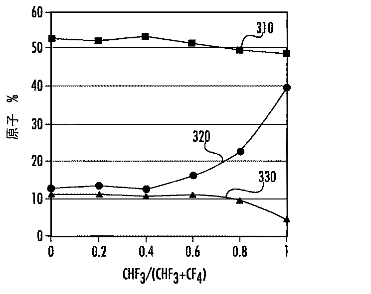
図5Aの例から、必要に応じてポリマーの付着と組み合わされた、ガラス表面の不均質なエッチングによって、シリコンおよび酸素が喪失され、アルカリ土類フッ化物が豊富な、フッ素および炭素が強化された表面を生じることで、例えばガラス(特に薄いガラス)等の他の高エネルギーの表面に対する、取り外し可能または解除可能な一時的な結合を容易に生じることができることがわかる。 From the example of FIG. 5A, heterogeneous etching of the glass surface, optionally combined with polymer deposition, resulted in loss of silicon and oxygen and enriched in fluorine and carbon rich in alkaline earth fluoride. It can be seen that creating a surface can easily produce a removable or releasable temporary bond to other high energy surfaces such as glass (especially thin glass).
複数の実施形態において、可撓制のガラスシートは、約50〜約300マイクロメートルの厚さを有してもよく、キャリアガラス物品は、約200マイクロメートル〜3mmの厚さを有してもよい。予想外なことに、このシリコンおよび酸素が喪失されフッ素および炭素が強化された表面は、約600℃を下回る温度では、ガラス表面に永久的に結合しない。 In embodiments, the flexible glass sheet may have a thickness of about 50 to about 300 micrometers, and the carrier glass article may have a thickness of about 200 micrometers to 3 mm. Good. Unexpectedly, this silicon and oxygen lost and fluorine and carbon enriched surface does not permanently bond to the glass surface at temperatures below about 600 ° C.
本明細書に記載される表面処理は、半導体における薄いウェハを処理するために、および/または、インターポーザプロセスのために用いられ得る。本発明の一部の例は、一般的に、より薄い基体の処理を可能にするために、より薄い基体に結合され取り外されるキャリアに関する。より具体的には、本発明の一部の例は、半導体および/またはインターポーザプロセスのために、ウェハをキャリアに結合し、そのようなプロセスの後、キャリアからウェハを剥離する方法および装置に関する。 The surface treatment described herein can be used to process thin wafers in semiconductors and / or for interposer processes. Some examples of the invention generally relate to a carrier that is bonded to and removed from a thinner substrate to allow processing of the thinner substrate. More specifically, some examples of the present invention relate to a method and apparatus for bonding a wafer to a carrier for semiconductor and / or interposer processes and peeling the wafer from the carrier after such a process.
半導体デバイスは、半導体ウェハ上または半導体ウェハ内に能動デバイスを形成することによって製造される。半導体ウェハは、例えば、ガラス、シリコン、ポリシリコン、単結晶シリコン、酸化シリコン、酸化アルミニウム、それらの組合せ等を含み得る。典型的には、単一のウェハ上に、数百または数千の集積回路(IC)またはダイが製造される。典型的には、ウェハ上に、複数の絶縁性、導電性、および半導電性材料層が順次付着され、パターニングされて、複数のICが形成される。一番上に形成される材料層の1つは、典型的には、その下のウェハ内の能動領域および構成要素に電気的に接続する結合パッドの層を含む。 Semiconductor devices are manufactured by forming active devices on or in a semiconductor wafer. The semiconductor wafer can include, for example, glass, silicon, polysilicon, single crystal silicon, silicon oxide, aluminum oxide, combinations thereof, and the like. Typically, hundreds or thousands of integrated circuits (ICs) or dies are fabricated on a single wafer. Typically, a plurality of insulating, conductive, and semiconductive material layers are sequentially deposited on the wafer and patterned to form a plurality of ICs. One of the material layers formed on the top typically includes a layer of bond pads that electrically connect to the active areas and components in the underlying wafer.
ICが形成された後、ウェハには裏面処理が施され得る。裏面処理は、ウェハをパッケージングに備えさせるためのウェハの薄化を含み得る。例えば、幾つかの技術では、裏面処理は、裏面の接点を設けるためにウェハを貫通するよう形成された、基体を貫通するビアへの電気的接続の形成を含み得る。この例では、ウェハの裏面は、例えば、ウェハの裏面上に導電性のビアを露出させるための研削等の処理によって薄化される。このウェハの薄化処理は、ウェハのエッジを損傷して、ウェハをより一層脆弱にし、その後のウェハの移送および処理中にウェハが損傷されやすくし得る。 After the IC is formed, the wafer can be subjected to backside processing. Backside processing may include wafer thinning to prepare the wafer for packaging. For example, in some techniques, the backside treatment can include the formation of electrical connections to vias through the substrate that are formed through the wafer to provide backside contacts. In this example, the back surface of the wafer is thinned by a process such as grinding to expose conductive vias on the back surface of the wafer. This wafer thinning process can damage the edge of the wafer, making the wafer even more fragile and making it susceptible to damage during subsequent wafer transport and processing.
これらのタイプの損傷を軽減するのを補助するために、ウェハにキャリアが取り付けられ得る。典型的には、以前には、このキャリアは接着剤を用いて取り付けられ、キャリアをハンドリングすることによってウェハのハンドリングを可能にすることが意図された。それに加えて、キャリアの強度が加えられることにより、移送および/または処理によって生じる応力がウェハを損傷しないように、ウェハが支持される。典型的なキャリアは、接着剤を用いてウェハに取り付けられたガラス基体であり得る。しかし、処理中にウェハが反る場合があること、および、典型的なキャリアは、反りを防止するのに十分な支持を与えないことがわかった。ウェハの反りの結果、処理が失敗する、および/または、アラーム状態を生じる場合がある。能動トランジスタ、抵抗器、およびRC回路、並びにトランジスタを相互接続するためのローカル配線が半導体にパターニングされる、IC製造の最初の部分は、FEOL(front-end-of-line)工程と称される。FEOL工程は、井戸の形成、ゲートモジュールの形成、ソースおよびドレインモジュールの形成、DRIE(反応性イオンドライエッチング)、TiまたはCu等のPVD、TiN等のCVD、SiO2等のPECVD、電解Cu(等)めっき、Cu(等)のアニール、計測(X−Ray等)、Cu(等)のCMP(化学機械的研磨)、Cu(H2O2+H2SO4)+Ti(DHF)ウェットエッチング、接着層(Ti等)のスパッタリング、シード層(Cu等)のスパッタリング、リソグラフィ(フォトレジスト、露光、剥離、Cuのエッチング)も含み得る。FEOL工程と関連づけられた幾つかの高温(例えば、500℃以上、一部の例では500℃〜650℃、および一部の例では高々700℃まで)処理に起因して、多くの接着剤系の溶液は、結合を維持できない場合があり、汚染物質となる気体を放出する場合があり、またはそれらの両方を生じ得るので、使用できない。多くの接着剤は、例えば300℃前後の遙かに低い温度でも気体を放出する。IC製造ラインの、個々のチップを横断してチップから外れた位置まで延びるより長い距離を接続する粗い配線が、ウェハ上の配線と相互接続される部分は、BEOL(back-end-of-line)配線工程と称される。BEOL工程は、チップ対パッケージの解決策のための、接点、絶縁層、相互接続配線、RFシールド、パッシベーション、ESD保護、結合パッド、および他の結合部位の形成のうち1以上も含み得る。BEOL工程の温度は、概してFEOL工程の温度よりも低いが、誘電材料の付着は、典型的には350〜450℃で行われ、ほとんどの接着剤は、これらのより低い温度でも気体を放出する。更に、ほとんどの一時的な接着剤は、ウェハおよびキャリアの材料とはミスマッチな高いCTEを有し、ウェハ上のデリケートな微細構造を完全なまま残しつつ除去するのは困難である。更に、接着剤とウェハおよび/またはキャリアの材料との間のCTEのミスマッチは、ウェハの望ましくない反りを生じ得る。更に、接着剤は、キャリアへの結合の際にインターポーザのビアに侵入して、ビアの少なくとも一部の金属配線を阻害し得るので望ましくない。 To help mitigate these types of damage, a carrier can be attached to the wafer. Typically, this carrier was previously attached with an adhesive and was intended to allow wafer handling by handling the carrier. In addition, the strength of the carrier is added to support the wafer so that stresses caused by transfer and / or processing do not damage the wafer. A typical carrier may be a glass substrate that is attached to the wafer using an adhesive. However, it has been found that the wafer may warp during processing and that typical carriers do not provide sufficient support to prevent warping. As a result of wafer warping, processing may fail and / or an alarm condition may occur. The first part of IC fabrication, where active transistors, resistors, and RC circuits, and local interconnects for interconnecting transistors are patterned into semiconductors, is called the front-end-of-line (FEOL) process. . FEOL process, formation of the well, formation of a gate module, forming the source and drain module, DRIE (reactive ion dry etching), PVD, such as Ti or Cu, CVD of TiN or the like, PECVD such as SiO 2, electrolytic Cu ( Etc.) Plating, Cu (etc.) annealing, measurement (X-Ray, etc.), Cu (etc.) CMP (chemical mechanical polishing), Cu (H 2 O 2 + H 2 SO 4 ) + Ti (DHF) wet etching, adhesive layer (Ti, etc.) sputtering, seed layer (Cu etc.) sputtering, lithography (photoresist, exposure, stripping, Cu etching) may also be included. Many adhesive systems due to some high temperature processing associated with the FEOL process (eg, above 500 ° C., in some examples 500 ° C. to 650 ° C., and in some cases up to 700 ° C.) This solution cannot be used because it may not be able to maintain binding and may emit polluting gases or both. Many adhesives release gas even at much lower temperatures, for example around 300 ° C. The portion of the IC manufacturing line where the coarse wiring connecting the longer distances extending across the individual chips and off the chip is interconnected with the wiring on the wafer is BEOL (back-end-of-line). ) Called wiring process. The BEOL process may also include one or more of the formation of contacts, insulation layers, interconnect wiring, RF shields, passivation, ESD protection, bond pads, and other bond sites for chip-to-package solutions. Although the temperature of the BEOL process is generally lower than the temperature of the FEOL process, the deposition of the dielectric material typically takes place at 350-450 ° C., and most adhesives release gas at these lower temperatures. . Furthermore, most temporary adhesives have a high CTE that is mismatched with the wafer and carrier materials and are difficult to remove while leaving the delicate microstructure on the wafer intact. Further, CTE mismatch between the adhesive and the wafer and / or carrier material can cause undesirable warping of the wafer. In addition, adhesives are undesirable because they can penetrate the vias of the interposer when bonded to the carrier and interfere with the metal wiring of at least some of the vias.
従って、処理条件、特にFEOL工程の高温の要求に耐えることができる改善されたキャリア基体の解決法の必要性がある。更に、FEOLの厳しさに耐えることができ、且つ、その後の容易な剥離を提供するキャリア基体の解決法は、最初からより薄い初期基体を用いることを可能にし、それにより、バックエンドの薄化の必要性を軽減する。即ち、典型的な既存の半導体ツールは、500マイクロメートル台以上のウェハを処理するよう設計されている。しかし、キャリアがウェハを支持している状態では、組み合わされた厚さがツールの処理厚さ範囲内にあればよい。従って、例えば、100マイクロメートルのウェハを支持するために、400マイクロメートルの厚さを有するキャリアが用いられてもよく、それらの組合せが、既存の半導体ツールにおいて処理され得る。本解決法では、高温処理の後でも容易な分離を可能にする制御された結合に起因して、基体として100マイクロメートルのウェハが用いられ得ることにより、ウェハ上へのデバイスの形成後の薄化による無駄および収率の低下の可能性が回避され得る。このFEOL工程に耐える能力は、200マイクロメートル以下(例えば、200、190、180、170、160、150、140、130、120、110、100、90、80、70、60、50、40、30、または20マイクロメートル)の厚さを有するウェハを最初から用いるキャリア基体の解決法を可能にする。そのような厚さ(例えば200マイクロメートル以下)のウェハが、キャリアに取り付けられ、処理され、次にキャリアから取り外され得る。これは、例えば、基体としてポリシリコンまたは単結晶シリコンウェハが用いられる場合には、非常に高価な材料の除去および無駄を回避でき、材料を、単に形成されたままの厚さで処理できるので、大きな利点となり得る。 Accordingly, there is a need for an improved carrier substrate solution that can withstand the processing conditions, particularly the high temperature requirements of the FEOL process. Furthermore, the carrier substrate solution that can withstand the FEOL severity and provides subsequent easy delamination allows the use of a thinner initial substrate from the beginning, thereby reducing the back end thinning. Reduce the need for. That is, typical existing semiconductor tools are designed to process wafers in the 500 micrometer range and above. However, with the carrier supporting the wafer, the combined thickness need only be within the processing thickness range of the tool. Thus, for example, to support a 100 micrometer wafer, a carrier having a thickness of 400 micrometers may be used, and combinations thereof can be processed in existing semiconductor tools. In this solution, a 100 micrometer wafer can be used as the substrate due to controlled bonding that allows easy separation even after high temperature processing, thereby reducing the thickness of the device after formation on the wafer. The possibility of waste and reduction in yield due to conversion can be avoided. The ability to withstand this FEOL process is 200 micrometers or less (eg, 200, 190, 180, 170, 160, 150, 140, 130, 120, 110, 100, 90, 80, 70, 60, 50, 40, 30 , Or 20 micrometers), which enables a carrier substrate solution to be used from the start. A wafer of such thickness (eg, 200 micrometers or less) can be attached to the carrier, processed, and then removed from the carrier. This is because, for example, when a polysilicon or single crystal silicon wafer is used as the substrate, removal and waste of very expensive material can be avoided, and the material can be processed with the thickness as it is formed, It can be a big advantage.
更に、半導体業界では、遙かに高価な先進的なリソグラフィによる解決法を必要とせずに、またはより多くの回路を収容するためのより大きなチップサイズを必要とせずに、半導体の性能を向上させるための主要な技術傾向として、3DIC技術が広く受け入れられている。この3DICのための技術は、薄化されたシリコンICに依拠していると共に、薄化されたICのスタック(3DIC)だけでなく平面状の構成(2.5DIC)においても、単一のインターポーザ上に直接配置された複数のIC間に電気的信号を再分配するためのインターポーザにも依拠している。 Furthermore, the semiconductor industry improves semiconductor performance without the need for much more expensive advanced lithographic solutions or the need for larger chip sizes to accommodate more circuits. As a major technological trend for, 3DIC technology is widely accepted. This technology for 3DIC relies on thinned silicon ICs, as well as a single interposer not only in thinned IC stacks (3DIC) but also in planar configurations (2.5DIC) It also relies on an interposer for redistributing electrical signals between a plurality of ICs placed directly above.
ポリシリコン、単結晶シリコン、またはガラスで作られ得るこれらのインターポーザは、経路長をミリメートル台からマイクロメートル台へと低減することにより、通信速度の劇的な改善を可能にする。この新たな技術の先頭を行く応用例は、例えば、Xilinx社(米国カリフォルニア州サンノゼ)によって製造されたハイエンドの特殊な機能性である、フィールドプログラマブルゲートアレイ(FPGA)である。 These interposers, which can be made of polysilicon, single crystal silicon, or glass, can dramatically improve communication speed by reducing the path length from millimeters to micrometers. A leading application for this new technology is the Field Programmable Gate Array (FPGA), a high-end special functionality manufactured by, for example, Xilinx (San Jose, Calif.).
インターポーザは、特徴的に、50um〜100um台の厚さと、今日では外径200mm〜300mmのサイズとを有し、長期にわたってより大きなサイズのパネルに向かう傾向がある。ビア(金属配線の後、ビアを通して電気的信号が処理される)は、外径5um〜150umであり、典型的には、設計および用途に応じて1平方ミリメートル当たり1〜20個のビア密度を有する。厚いインターポーザは、許容できない形状因子(高さ)および性能的(熱的)支障を生じるので、インターポーザは本質的に薄い。薄いとは、一般的に、100マイクロメートル前後であると見なされるが、一般的には200マイクロメートルを超えない。一方、国際半導体技術ロードマップ(ITRS)は、50umまでの厚さを考慮している。繰り返すが、これらの厚さの基体は、一般的に、既存のツールでは処理できない。従って、本開示は、キャリア、特に、高温処理中でもウェハに取り付けられたまま耐え得ると共に、そのような処理後のウェハの容易な取り外しを可能にするキャリアを、有利に使用することを考えたものである。 Interposers characteristically have thicknesses on the order of 50 um to 100 um and today are sized with an outer diameter of 200 mm to 300 mm, and tend towards larger size panels over time. Vias (after electrical wiring, electrical signals are processed through the vias) have an outer diameter of 5 um to 150 um, and typically have a density of 1-20 vias per square millimeter depending on design and application. Have. A thick interposer is inherently thin because it causes unacceptable form factor (height) and performance (thermal) impediments. Thin is generally considered to be around 100 micrometers, but generally does not exceed 200 micrometers. On the other hand, the International Semiconductor Technology Roadmap (ITRS) considers thicknesses up to 50 um. Again, these thick substrates are generally not processable with existing tools. Accordingly, the present disclosure contemplates the advantageous use of carriers, particularly carriers that can withstand being attached to a wafer even during high temperature processing and that allow for easy removal of the wafer after such processing. It is.
インターポーザ技術は新しいものであるが、主なインターポーザ基体は単結晶シリコンであり、ガラスが代替物として登場している。ガラスの魅力は性能およびコストであるが、ガラスのこれらの長所を実現する解決法は、今日ではまだ存在しない。本開示の概念は、IC、RC回路、およびインターポーザを含む様々なデバイスを提供するために、ウェハとしての、シリコンおよびガラスを含む様々な薄い基体の、FEOLおよびBEOLを含む様々な条件下での処理を可能にする。 Interposer technology is new, but the main interposer substrate is single crystal silicon, and glass has emerged as an alternative. The appeal of glass is performance and cost, but no solution exists today that realizes these advantages of glass. The concept of the present disclosure is based on various thin substrates, including silicon and glass, as a wafer, under various conditions, including FEOL and BEOL, to provide various devices including ICs, RC circuits, and interposers. Enable processing.
本開示の結合の解決法は、既存の必要な処理工程の全てを通して、最終的な厚さのガラス、および薄化されたシリコンの薄い形状の処理を、高い収率および短い処理時間で可能にする。薄いウェハが、金属配線、分配層の配置によって処理された後、ウェハは、薄化および処理されたインターポーザ、および/またはICを完全なまま残して剥離され得る。更に、既に薄化された(200マイクロメートル以下台の)シリコンウェハと共にキャリアを使用することは、ウェハ上に任意のデバイスが加工される前に、ウェハをスクリーニングすることを可能にする。従って、コストの低減、および/または収率の改善が可能である。 The bonding solution of the present disclosure allows for final thickness glass and thin silicon thin shape processing with high yield and short processing time through all of the existing required processing steps. To do. After a thin wafer is processed by metal wiring, distribution layer placement, the wafer can be stripped leaving the thinned and processed interposer, and / or IC intact. Furthermore, using the carrier with an already thinned silicon wafer (on the order of 200 micrometers or less) allows the wafer to be screened before any devices are processed on the wafer. Therefore, cost reduction and / or improvement in yield are possible.
上記に鑑みて、(シート−キャリア物品が用いられる半導体プロセスまたはディスプレイ製造プロセスには不適合な気体を放出せずに)高温処理を含むFEOL工程の厳しさに耐えることができながら、キャリアからの薄いシートの全体の除去を(一度に全部、または部分毎に)可能にする、薄いシート−キャリア物品の必要性がある。本明細書は、FEOL工程(高温処理を含む)に耐えるのに十分に強いが、高温処理後でもキャリアからのシートの剥離を可能にするのに十分に弱い、一時的な結合を生じるために、キャリアと薄いシートとの接着を制御するための表面処理について説明する。より具体的には、本開示は、薄いシートとキャリアとの室温におけるファン・デル・ワールス結合および/または水素結合、並びに高温における共有結合を制御するために、薄いシート、キャリア、またはそれらの両方に設けられ得る表面処理を提供する。更に具体的には、室温における結合は、真空処理中、湿式処理中、および/または超音波クリーニング処理中に、薄いシートとキャリアとを一体に保持するのに十分となるよう制御され得る。同時に、高温における共有結合は、高温処理中の薄いシートとキャリアとの永久的な結合を防止するよう、および高温処理中の剥離を防止するのに十分な結合を維持するよう制御され得る。 In view of the above, while being able to withstand the rigors of FEOL processes, including high temperature processing (without releasing gases that are incompatible with the semiconductor or display manufacturing processes in which the sheet-carrier article is used), the thin from the carrier There is a need for a thin sheet-carrier article that allows the entire removal of the sheet (all at once or part by part). This specification is intended to produce a temporary bond that is strong enough to withstand the FEOL process (including high temperature processing), but weak enough to allow peeling of the sheet from the carrier even after high temperature processing. The surface treatment for controlling the adhesion between the carrier and the thin sheet will be described. More specifically, the present disclosure provides for thin sheet, carrier, or both to control van der Waals and / or hydrogen bonding at room temperature between thin sheet and carrier, and covalent bonding at high temperature. A surface treatment that can be provided is provided. More specifically, bonding at room temperature can be controlled to be sufficient to hold the thin sheet and carrier together during vacuum processing, wet processing, and / or ultrasonic cleaning processing. At the same time, covalent bonding at high temperatures can be controlled to prevent permanent bonding between the thin sheet and the carrier during high temperature processing and to maintain sufficient bonding to prevent delamination during high temperature processing.
一時的な結合状態を生じる表面処理の別の用途は、例えばFEOL工程のように、400℃以上(例えば、≧450℃、≧500℃、≧550℃、≧600℃)の温度を必要とするプロセスにおいて薄いシートを処理するために、キャリア上の薄いシートを用いることに備えるものである。即ち、薄いシートは、後で薄化させる必要がない厚さで処理されるウェハであり得る。本明細書に記載される表面処理は、そのような温度条件下でのキャリアの再使用を提供するために用いられ得る。具体的には、これらの表面処理は、処理後に、薄いシート全体がキャリアから分離され得るように、薄いシートとキャリアとの一時的な結合を生じるために用いられ得る。薄いシートは、一度に全部分離されてもよく、または部分毎に分離されてもよい。例えば、まず、薄いシートの一部の上に製造されたデバイスを取り外し、その後、例えばキャリアを再使用のためにクリーニングするために、残りの部分(あれば)を除去する。薄いシート全体を除去することによって、または、合わせると薄いシート全体になる薄いシートの細切れにされた部分を除去することによって、薄いシートの全てがキャリアから除去された場合には、単に別の薄いシートをキャリア上に配置することによって、キャリアを再使用できる。或いは、キャリアは、クリーニングされて、新たな表面処理を生じることによって、薄いシートを担持するよう再び整えられてもよい。この表面処理は、薄いシートとキャリアとの一時的な結合を設けるので、温度が600℃以上の処理のために用いられ得る。当然ながら、これらの表面処理は、600℃以上の温度での処理中の結合表面エネルギーを制御し得るが、例えば400℃以上の温度(例えば、≧450℃、≧500℃、≧550℃)等のより低い温度での処理に耐える薄いシートおよびキャリアの組合せを製造するためにも用いられてもよく、例えばBEOL工程において、そのようなより低い温度を加える際に、結合を制御するために用いられてもよい。薄いシートは、200マイクロメートル以下の厚さを有するポリシリコンもしくは単結晶シリコンウェハ、シリコンウェハ、ガラス、セラミック、ガラス−セラミック、クオーツ、サファイアであってもよく、FEOL工程において、RC回路、IC、または他の電子デバイスをその上に形成するために、例えば500℃以上の温度で処理され得る。FEOL工程の後、このウェハは、電子デバイスを損傷することなく容易にキャリアから取り外され得る。しかし、取り外される前に、ウェハには、例えばBEOL工程のような、より低い温度での処理が施され得る。 Another application of surface treatment that creates a temporary bonded state requires temperatures of 400 ° C. or higher (eg, ≧ 450 ° C., ≧ 500 ° C., ≧ 550 ° C., ≧ 600 ° C.), such as in the FEOL process. It provides for using a thin sheet on a carrier to process a thin sheet in the process. That is, a thin sheet can be a wafer that is processed at a thickness that does not need to be thinned later. The surface treatment described herein can be used to provide for carrier reuse under such temperature conditions. Specifically, these surface treatments can be used to create a temporary bond between the thin sheet and the carrier so that after treatment, the entire thin sheet can be separated from the carrier. Thin sheets may be separated all at once, or may be separated piece by piece. For example, the device fabricated on a portion of the thin sheet is first removed, and then the remaining portion (if any) is removed, for example to clean the carrier for reuse. If all of the thin sheet is removed from the carrier by removing the entire thin sheet, or by removing the shredded portion of the thin sheet that, when combined, becomes the entire thin sheet, it is simply another thin. By placing the sheet on the carrier, the carrier can be reused. Alternatively, the carrier may be reconditioned to carry a thin sheet by cleaning and creating a new surface treatment. This surface treatment provides a temporary bond between the thin sheet and the carrier and can be used for treatments where the temperature is 600 ° C. or higher. Of course, these surface treatments can control the binding surface energy during processing at temperatures above 600 ° C., for example, temperatures above 400 ° C. (eg, ≧ 450 ° C., ≧ 500 ° C., ≧ 550 ° C.), etc. It may also be used to produce thin sheet and carrier combinations that can withstand lower temperature processing, such as in BEOL processes, used to control bonding when applying such lower temperatures. May be. The thin sheet may be a polysilicon or single crystal silicon wafer having a thickness of 200 micrometers or less, a silicon wafer, glass, ceramic, glass-ceramic, quartz, sapphire. In the FEOL process, an RC circuit, IC, Or it may be processed at a temperature of, for example, 500 ° C. or higher to form other electronic devices thereon. After the FEOL process, the wafer can be easily removed from the carrier without damaging the electronic device. However, prior to removal, the wafer may be processed at a lower temperature, such as a BEOL process.
一時的な結合を設けるための表面処理の第2の用途は、インターポーザを製造することである。この場合には、薄いシートは、例えばシリコン、ポリシリコン、単結晶シリコン、ガラス、セラミック、ガラス−セラミック、クオーツ、サファイアを含む任意の適切な材料でできた、例えば200マイクロメートル以下の厚さを有し得るウェハであり得る、インターポーザである。 A second use of surface treatment to provide temporary bonding is to produce interposers. In this case, the thin sheet is made of any suitable material including, for example, silicon, polysilicon, single crystal silicon, glass, ceramic, glass-ceramic, quartz, sapphire, and has a thickness of, for example, 200 micrometers or less. An interposer that may be a wafer that may have.
ここで、インターポーザの一例、およびその製造について、図6〜図8を参照して説明する。 Here, an example of an interposer and its manufacture will be described with reference to FIGS.
図6を参照すると、薄いシート20は、制御された結合領域40、即ち、薄いシート20とキャリア10との間に一時的な結合が生じる領域によって、キャリア10に結合され得る。
With reference to FIG. 6, the
この実施形態では、キャリア10は、ガラス基体であってもよく、または、ガラスと類似の表面エネルギーを有する別の適切な材料(例えば、シリコン、ポリシリコン、単結晶シリコン、セラミック、ガラス−セラミック、サファイア、もしくはクオーツ)であってもよい。ガラス基体を用いることの長所は、最小限の厚さのばらつきを有する平坦なシートを比較的低コストで得ることができ、高価なキャリア基体の必要性を回避できることである。更に、ガラスを用いると、コスト効果的な方法で高品質を達成できる。即ち、非常に均一な厚さのガラス基体を非常に安価に製造して、キャリアとして用いることができる。しかし、本開示の表面処理を用いれば、キャリアは、ウェハが最終的な厚さまで薄化される場合のように、合計厚さのばらつきが低い高精度のキャリアである必要はない。即ち、キャリア上のウェハが薄化される際には、キャリアにばらつきがあると、薄化の際に、そのばらつきが薄化されたウェハに表れるので、キャリアは、合計厚さのばらつきに関して非常に緊密に制御されなければならない。ウェハが既に最終的な厚さである場合に、ウェハ上でのデバイスの形成を可能にする本開示の表面処理を用いれば、キャリアの合計厚さのばらつきの重要性は遙かに低くなる。
In this embodiment, the
この実施形態では、薄いシート20を用いて、インターポーザ56を形成する。シートは、例えば、ポリシリコンもしくは単結晶シリコンウェハを含むシリコン、クオーツ、サファイア、セラミック、またはガラスであり得る。シート20は、200マイクロメートル以下の厚さを有し得る。外周52およびビアのアレイ50を有する各インターポーザ56において、アレイ50は外周57を有する。10個のインターポーザ56が示されているが、1を含む任意の適切な数が、薄いシート20上に配設され得る。図示の便宜上、各インターポーザ56は、ビアのアレイ50を1つのみ有するものとして示されているが、必ずしもそうである必要はなく、むしろ、任意のインターポーザ56が、2以上のアレイ50を有してもよい。更に、各インターポーザは、同じ数のアレイ50を有するものとして示されているが、必ずしもそうである必要はなく、任意の数(0を含む)のインターポーザが同じ数のアレイ50を有してもよい。更に、アレイ50は、典型的には同じ数およびパターンのビアを有するが、必ずしもそうである必要はない。図示の便宜上、インターポーザ56の1つの1つのみのアレイ50に複数のビア60が示されているが、必ずしもそうである必要はなく、即ち、残りのインターポーザ56の任意の1以上が、複数のビア60の1以上のアレイ50を有してもよい。
In this embodiment, the
ここで、図6の線7−7に沿った断面図である図7を参照する。ビア60は、貫通ビアまたはブラインドビア(即ち、シート20の厚さ以内で終端するビア)を含み得る。ビア60は直径62を有し、ピッチ64で離間されている。直径62は同じものとして示されているが、必ずしもそうである必要はなく、即ち、1つのインターポーザ56上の1つのアレイ50または異なるアレイ50に、異なる直径のビアが存在してもよい。直径62は、例えば5マイクロメートル〜150マイクロメートルであり得る。同様に、ビア62は同じピッチ64で離間されているが、必ずしもそうである必要はなく、即ち、1つの薄いシート20上の1つのインターポーザ56または異なるインターポーザ56上の1つのアレイ50または異なるアレイ50に、異なるピッチが存在してもよい。ピッチは、例えば、1平方ミリメートル当たり1〜20個のビアがあるピッチであってもよく、インターポーザの設計および用途に応じて異なる。更に、ビア60の任意の1以上に、材料61が存在し得る。材料61は、電気的に導電性の材料、電気的に絶縁性の材料、またはそれらの組合せであり得る。例えば、ビアの外周、即ち外径62に導電性の材料が形成されてもよく、ビアの残りの部分を埋めるために、異なる導電性の材料または絶縁性の材料が用いられ得る。
Reference is now made to FIG. 7, which is a cross-sectional view taken along line 7-7 of FIG. Via 60 may include a through via or a blind via (ie, a via that terminates within the thickness of sheet 20). The
次に、図7に示されている図と類似の図8を参照するが、ここでは、インターポーザ56上にデバイス/構造が配設され、ビア60に接続されている。図8に示されるように、1つのデバイス66は、複数のビア60上に配設されて、それらと接続され得る。デバイス66は、シリコン、シリコン−ゲルマニウム、ガリウムヒ素、および窒化ガリウムから製造された、集積回路、MEMS、マイクロセンサ、パワー半導体、発光ダイオード、フォトニック回路、CPU、SRAM、DRAM、eDRAM、ROM、EEPROM、フラッシュメモリ、インターポーザ、埋込型受動デバイス、および微小デバイスを含み得る。1つのデバイス66のみが示されているが、1つのインターポーザ56上に、デバイスのアレイ56を含む任意の適切な数のデバイス66が存在し得る。或いは、構造物68が、1つのビア60のみの上に配設されて、そのビア60と接続され得る。構造物68は、はんだのバンプ、金属のポスト、金属の柱、相互接続ルーティング、相互接続ライン、絶縁酸化物層、並びに、シリコン、ポリシリコン、二酸化シリコン、(酸)窒化シリコン、金属(例えば、Cu、Al、W)、低k誘電材料、ポリマー誘電材料、金属窒化物、および金属ケイ化物からなる群から選択される材料で形成された構造を含み得る。1つの構造物68のみが示されているが、1つのインターポーザ56上に、構造のアレイ56を含む任意の適切な数の構造物68が存在し得る。更に、デバイス66上には1以上の構造物68が配設され得る。
Reference is now made to FIG. 8, which is similar to the view shown in FIG. 7, where the device / structure is disposed on the
制御された結合領域40において、キャリア10と薄いシート20とは、重なった領域全体にわたってキャリア10と薄いシート20とが接続されるが、高温処理、例えば400℃以上(例えば、≧450℃、≧500℃、≧550℃、≧600℃、および高々約650℃、または一部のケースでは700℃まで)の温度における処理の後でも、互いから分離され得るように、互いに結合される。
In the controlled
本明細書に開示される表面処理は、キャリア10と薄いシート20との間に一時的な結合領域40を設けるための界面結合層30を生じる。具体的には、これらの表面処理は、キャリア10上または薄いシート20上のアレイ50の外周52内に形成され得る。従って、デバイスプロセス中に物品2が高温で処理される際、外周52によって境界される領域内において、キャリア10と薄いシート20との一時的な結合が設けられてもよく、この一時的な結合により、分離する力を加えれば、この領域内において薄いシートとキャリアとが(薄いシートまたはキャリアを壊滅的に損傷することなく)分離され得るが、超音波処理を含むプロセス中には、薄いシートとキャリアとは剥離しない。更に、界面結合層30の非常に小さい厚さ(即ち、100ナノメートル未満、40ナノメートル未満、10ナノメートル未満、および一部の例では約2ナノメートル)を理由として、(即ち、40〜60マイクロメートル台以上のより厚い接着剤層の場合のような)ウェハと表面処理との間のCTEのミスマッチに起因するウェハに対する影響は無い。
The surface treatment disclosed herein produces an
そして、外周52を有する(ビア60のアレイ50を各々が有する)インターポーザ56の抽出時には、外周52内の薄いシート20の部分は、処理後および外周52に沿った薄いシートの分離後に、単に、キャリア10から分離され得る。或いは、薄いシート20(或いは、薄いシート20およびキャリア10の両方)は、線5に沿ってダイスカットされてもよく、それにより、キャリア10から、または、キャリアが薄いシート20と共にダイスカットされる場合には、キャリア10の断片から、インターポーザ56の外周52より大きい薄いシート20の部分が取り外されてもよい。表面処理は、薄いシートとキャリアとの一時的な結合を設けるので、温度が600℃以上であるプロセスのために用いられ得る。当然ながら、これらの表面処理は、600℃以上の温度における処理中の結合表面エネルギーを制御し得るが、これらは、例えば400℃以上(例えば≧450℃、≧500℃、≧550℃)のより低い温度における処理に耐える薄いシートとキャリアとの組合せを製造するために用いられてもよく、そのようなより低い温度の用途において用いられ得る。
And when extracting an
複数の実施形態において、シート20は、シリコン、クオーツ、サファイア、セラミック、またはガラスを含む。
In embodiments, the
複数の実施形態において、シート20の厚さは200マイクロメートル以下である。
In embodiments, the thickness of the
複数の実施形態において、シート20は、少なくとも1つのビアを更に含む。複数の実施形態において、少なくとも1つのビアは、150マイクロメートル以下の直径を有する。複数の実施形態において、少なくとも1つのビアは、電気的に導電性の材料をビア内に含み得る。
In embodiments, the
複数の実施形態において、シート20は、キャリア10に一時的に結合された表面とは反対側のデバイス表面を含み、デバイス表面は、シリコン、シリコン−ゲルマニウム、ガリウムヒ素、および窒化ガリウム上に、またはそれらで製造された、集積回路、MEMS、CPU、マイクロセンサ、パワー半導体、発光ダイオード、フォトニック回路、インターポーザ、埋込型受動デバイス、および微小デバイスからなる群から選択されるデバイスのアレイを含む。
In embodiments, the
複数の実施形態において、シート20は、キャリア10に一時的に結合された表面とは反対側のデバイス表面を含み、デバイス表面は、はんだのバンプ、金属のポスト、金属の柱、相互接続ルーティング、相互接続ライン、絶縁性酸化物層、並びに、シリコン、ポリシリコン、二酸化シリコン、シリコン(酸)窒化物、金属、低k誘電材料、ポリマー誘電材料、金属窒化物、および金属ケイ化物からなる群から選択される材料で形成された構造物からなる群から選択される、少なくとも1つの構造物を含む。
In embodiments, the
複数の実施形態において、界面結合層30の厚さは0.1〜100nmである。
In some embodiments, the
複数の実施形態において、キャリアとシートとは、100平方cmの面積にわたって一時的に結合される。 In embodiments, the carrier and the sheet are temporarily bonded over an area of 100 square centimeters.
複数の実施形態において、シート20とキャリア10とは一時的に一体に結合され、FEOL工程を受ける。複数の実施形態において、FEOL工程は、500℃〜700℃の処理チャンバ温度を含む。複数の実施形態において、FEOL工程は、DRIE(反応性イオンドライエッチング)、PVD、TiNのCVD、SiO2のPECVD、電解Cuめっき、Cuのアニール、計測、CuのCMP、Cu(H2O2+H2SO4)+Ti(DHF)のウェットエッチング、接着層のスパッタリング、シード層のスパッタリング、リソグラフィ(フォトレジスト、露光、剥離、Cuのエッチング)のうち少なくとも1つを含む。
In embodiments, the
以下の実施例は、上述の一般的な手順に従った、本開示の積層ガラス製品の製造、使用、および分析を示す。また、以下の実施例は、積層体物品の構成要素部品間の界面結合の、得られる強度を制御する能力も示す。 The following examples illustrate the manufacture, use, and analysis of the laminated glass product of the present disclosure following the general procedure described above. The following examples also show the ability to control the resulting strength of the interfacial bond between the component parts of the laminate article.
実施例1
キャリアのクリーニング
キャリアは、本開示の処理において用いられる前、本開示の処理において用いられた後にガラス被加工物が剥離または分離された後、またはそれらの両方において、クリーニンされ得る。クリーニング工程は、例えば、脱イオン水によるすすぎ、NH4OH:H2O2:H2O混合物、O2プラズマ処理、酸によるすすぎ(即ち、HClまたはHCl:H2O2)、および類似のすすぎ、またはそれらの組合せのうち1以上を含み得る。クリーニング工程は、主に、クリーニングされた表面上の粒子の濃度を大きく抑制することに関係している。
Example 1
Cleaning the carrier The carrier can be cleaned before being used in the process of the present disclosure, after being used in the process of the present disclosure, after the glass workpiece has been peeled or separated, or both. The cleaning step can be, for example, rinsing with deionized water, NH 4 OH: H 2 O 2 : H 2 O mixture, O 2 plasma treatment, acid rinsing (ie, HCl or HCl: H 2 O 2 ), and the like One or more of rinsing or combinations thereof may be included. The cleaning process is primarily concerned with greatly reducing the concentration of particles on the cleaned surface.
実施例2
表面処理
本開示の足し算的な表面処理プロセスにおいては、キャリアまたはガラス被加工物の表面は、共有結合をなくしまたは抑制しつつ、ファン・デル・ワールス結合を可能にするよう改質され得る。処理された表面は、高々中等度の処理温度(例えば、600℃)までのキャリアと被加工物との接着安定性を提供する。表面処理は、例えば、50mTorr(約6.7パスカル)の真空圧力、25sccmのCHF3および25sccmのCF4反応物質流量および濃度、200WRFの出力、並びに、60秒のフッ素プラズマへの露出または処理時間という処理条件を有するフッ素プラズマを用いて達成され得る。或いは、エッチャントとしてのCF4およびフッ素ポリマー形成剤としてのC4F8を有するICPプラズマ構成において、または、エッチャントとしてのCF4およびフッ素ポリマー形成剤としてのCH4を有するRIEチャンバ内で、または、エッチャントとしてのCF4およびポリマー形成剤としてのH2を有するRIEチャンバ内で、類似の表面が整えられ得る。
Example 2
Surface Treatment In the additive surface treatment process of the present disclosure, the surface of the carrier or glass workpiece can be modified to allow van der Waals bonding while eliminating or suppressing covalent bonding. The treated surface provides adhesion stability between the carrier and the workpiece up to at most moderate processing temperatures (eg, 600 ° C.). Surface treatments include, for example, a vacuum pressure of 50 mTorr (about 6.7 Pascals), 25 sccm of CHF 3 and 25 sccm of CF 4 reactant flow rate and concentration, 200 WRF output, and 60 seconds of exposure to fluorine plasma or treatment time. Can be achieved using a fluorine plasma having the following processing conditions. Or in an ICP plasma configuration with CF 4 as the etchant and C 4 F 8 as the fluoropolymer former, or in an RIE chamber with CF 4 as the etchant and CH 4 as the fluoropolymer former, or Similar surfaces can be trimmed in an RIE chamber with CF 4 as the etchant and H 2 as the polymer former.
別の例では、結合される対応する被加工物は、例えば、半導体基体またはエピタキシャル成長のための基体(例えばシリコン、ガリウムヒ素、またはサファイア等)であり得る。これらの基体は、手作業による結合またはローラによる積層によって、上述の薄いガラス基体と同様の処理されたキャリアガラスに結合される。これらの基体材料の接着は、上述の、結合された際および熱処理後のガラス基体と同様であった。 In another example, the corresponding workpiece to be bonded can be, for example, a semiconductor substrate or a substrate for epitaxial growth (such as silicon, gallium arsenide, or sapphire). These substrates are bonded to a treated carrier glass similar to the thin glass substrate described above by manual bonding or roller lamination. The adhesion of these substrate materials was similar to the glass substrates when bonded and after heat treatment as described above.
実施例3
キャリア基体への薄いガラス被加工物の結合
例示的な結合手順においては、薄いガラス被加工物を、上述の例における処理の任意のものを用いて処理されたキャリア表面と軽く接触させた。例えば、機械的な供給源または類似の供給源からの接触圧力が、薄いガラス被加工物およびキャリアの一方または両方の1以上の点に加えられ得る。軽く加えられた圧力が、結合の波面を開始させ得る。
Example 3
Bonding a Thin Glass Workpiece to a Carrier Substrate In an exemplary bonding procedure, a thin glass workpiece was lightly contacted with a carrier surface that was processed using any of the processes in the above example. For example, contact pressure from a mechanical source or similar source can be applied to one or more points on one or both of the thin glass workpiece and the carrier. A lightly applied pressure can initiate the wavefront of the bond.
別の例の結合手順においては、結合は、例えば、ローラ積層アセンブリを用いて、処理されていないまたは処理された薄いガラス被加工物を、処理されたキャリアに施すことによる、従来の機械的な積層方法によって達成され得る。 In another example bonding procedure, bonding is accomplished by conventional mechanical, for example, by applying a thin glass workpiece that has not been processed or has been processed to a processed carrier using a roller laminate assembly. It can be achieved by a lamination method.
実施例4
結合された薄いガラス被加工物上でのデバイス(例えば、フラットパネルディスプレイ)製造
デバイスプロセス、即ち、作製、製造、改質等は、従来のプロセス技術を用いて、結合された薄いガラス被加工物の外側の結合されていない表面上において、結合されていない薄いガラス被加工物の表面の、デバイス、回路、または類似の構造的な改質または表面改質が生じるように、達成され得る。デバイスプロセスは、例えば、酸、塩基、真空、膜蒸着、プラズマエッチング、高温アニール真空、および類似の処理工程に対する露出を含み得る。
Example 4
Device (e.g., flat panel display) manufacturing device processes on bonded thin glass workpieces , i.e., fabrication, manufacturing, modification, etc. are performed using conventional process techniques to bond thin glass workpieces. Can be achieved such that a device, circuit, or similar structural or surface modification of the surface of the unbonded thin glass workpiece occurs on the unbonded surface on the outside. Device processes can include, for example, exposure to acids, bases, vacuum, film deposition, plasma etching, high temperature anneal vacuum, and similar processing steps.
実施例5
剥離
剥離処理は、この時点ではデバイスプロセスを受けた外面を有する、結合された薄いガラス被加工物、即ち、デバイスで改質されたガラス基体を、機械的に、比較的容易に、キャリア基体から取り外すことを可能にする。キャリアからの取り外しは、任意の適切な装置または方法(例えば、真空吸着を用いてコーナー部を把持し、結合された薄いガラス被加工物をキャリアから(例えば剥離することによって)取り外すよう引っ張ること)によって達成され得る。
Example 5
The delamination process now mechanically and relatively easily removes a bonded thin glass workpiece, i.e., a device-modified glass substrate, having an outer surface that has undergone a device process from a carrier substrate. Allows removal. Removal from the carrier can be any suitable device or method (eg, using vacuum suction to grip the corners and pulling the bonded thin glass workpieces off the carrier (eg, by peeling)). Can be achieved.
実施例6
表面組成を決定するXPS法
X線光電子分光法(XPS)を用いて、全ての表面の表面組成および化学種を調査および測定した。全てのXPSデータは、市販のXPS機器(PHI)を用いて、AlKα線および45度のX線取出角を用いて収集された。XPS機器のベンダーによって提供されているソフトウェアおよび感度因子を用いて、スペクトルを分析した。表面組成を決定するために、Si2p、Al2p、O1s、C1s、Mg2s、Ca2s、B1s、F1s、およびSr3dの軌道を用いた。これらの元素の報告された濃度は、XPS信号の探査深さ全体にわたる各元素の濃度の平均とした。
Example 6
XPS method to determine surface composition X-ray photoelectron spectroscopy (XPS) was used to investigate and measure the surface composition and chemical species of all surfaces. All XPS data was collected using a commercial XPS instrument (PHI) with AlKα radiation and 45 degree X-ray extraction angle. The spectra were analyzed using software and sensitivity factors provided by XPS instrument vendors. In order to determine the surface composition, Si2p, Al2p, O1s, C1s, Mg2s, Ca2s, B1s, F1s, and Sr3d trajectories were used. The reported concentrations of these elements were the average of the concentration of each element over the XPS signal exploration depth.
実施例7
CHF 3 (フッ素ポリマー形成剤)とCF 4 (エッチャント)との比率の関数としての表面組成の変化
表1は、未処理の「EXG」ガラス、およびCF4とCHF3との比率が異なるプラズマ処理後の「EXG」ガラスについての、図4から得られた選択された原子の表面原子比率(Al:Si、Ca:Si、Mg:Si、Sr:Si)を示す。これらのデータは、未処理の「EXG」表面と比較した、処理された「EXG」表面について、プラズマ表面処理が、Al:Si、Ca:Si、Mg:Si、およびSr:Siの原子比率の実質的な増加を生じることをはっきりと示しており、これらの結果は、Al、Ca、Mg、およびSrと比較してSiが相対的に喪失されていることを示す。
Example 7
Changes in surface composition as a function of the ratio of CHF 3 (fluoropolymer former) and CF 4 (etchant) Table 1 shows untreated “EXG” glass and plasma treatment with different ratios of CF 4 and CHF 3 FIG. 6 shows the surface atomic ratios of selected atoms obtained from FIG. 4 (Al: Si, Ca: Si, Mg: Si, Sr: Si) for a later “EXG” glass. These data show that for the treated “EXG” surface compared to the untreated “EXG” surface, the plasma surface treatment is of atomic ratios of Al: Si, Ca: Si, Mg: Si, and Sr: Si. It is clearly shown that a substantial increase occurs, and these results indicate that Si is relatively lost compared to Al, Ca, Mg, and Sr.
炭素質の上層の存在は、異なる軌道から発せられたXPS信号の選択的な減衰に起因して、下層の元素の原子比率に影響することが知られている。Ca:Siの比率においては、測定のアーチファクトに起因する変化は小さく、Al:Si、Mg:Si、およびSr:Siの比率においては、これらの変化は最小であり、検出限界より本質的に低い。 The presence of a carbonaceous upper layer is known to affect the atomic ratio of the lower layer elements due to selective attenuation of XPS signals emanating from different orbitals. At Ca: Si ratios, the changes due to measurement artifacts are small, and at Al: Si, Mg: Si, and Sr: Si ratios these changes are minimal and essentially below the detection limit. .
実施例8
ガラス表面上のフッ化物種の生成の判定
また、XPSを用いて、表面上で検出されたフッ素の化学種分析を行った。F1sスペクトルのピークは、約1.9eVだけ分離された区別できる2つのピークでフィッティングできた。低い方の結合エネルギーのピークは、金属フッ化物種として存在するフッ素に割り当てられ、高い方の結合エネルギーピークは、炭素質の層と反応したフッ素に割り当てられた。このようにして、XPSによって、金属フッ化物に起因する表面上で検出されたフッ素濃度の割合、およびフッ素ポリマー層中に存在するフッ素の割合を得ることができる。
Example 8
Determination of the generation of fluoride species on the glass surface Also, using XPS, chemical species analysis of fluorine detected on the surface was performed. The peaks of the F1s spectrum could be fitted with two distinct peaks separated by about 1.9 eV. The lower binding energy peak was assigned to fluorine present as the metal fluoride species, and the higher binding energy peak was assigned to fluorine that reacted with the carbonaceous layer. In this way, XPS can obtain the proportion of fluorine concentration detected on the surface due to the metal fluoride and the proportion of fluorine present in the fluoropolymer layer.
XPSによって検出された、金属フッ化物の形態のフッ素の濃度を知ること、および、カチオンの合計濃度を知ることで、合計のフッ素とカチオンとの比率を計算することが可能である。この例では、合計カチオン濃度は、実施例7において定めた条件下で、XPSによって検出されたB、Al、Mg、Sr、Si、およびCaの合計濃度として定義される。純粋なCHF3および純粋なCF4のプラズマ条件の例についての、このような分析の結果が、表2に示されている。 Knowing the concentration of fluorine in the form of metal fluoride detected by XPS, and knowing the total concentration of cations, it is possible to calculate the total fluorine to cation ratio. In this example, the total cation concentration is defined as the total concentration of B, Al, Mg, Sr, Si, and Ca detected by XPS under the conditions defined in Example 7. The results of such an analysis for examples of pure CHF 3 and pure CF 4 plasma conditions are shown in Table 2.
表2の結果は、純粋なCHF3の例については、XPSによって検出された表面上のフッ素濃度の大半はフッ素ポリマーの形態であり、一方、純粋なCF4の例においては、XPSによって検出されたフッ素濃度の大半はフッ素ポリマーの形態であることを示している。 The results in Table 2 show that for the pure CHF 3 example, the majority of the fluorine concentration on the surface detected by XPS is in the form of a fluoropolymer, while in the pure CF 4 example it is detected by XPS. The majority of the fluorine concentration indicates that it is in the form of a fluoropolymer.
様々な具体的な実施形態および技術を参照して、本開示を説明した。しかし、本開示の範囲内に留まりつつ、多くの変更および変形が可能であることを理解されたい。 The present disclosure has been described with reference to various specific embodiments and techniques. However, it should be understood that many modifications and variations are possible while remaining within the scope of the present disclosure.
以下、本発明の好ましい実施形態を項分け記載する。 Hereinafter, preferable embodiments of the present invention will be described in terms of items.
実施形態1
ガラスキャリア基体上に支持された、デバイスで改質された基体を有するデバイス基体物品を製造する方法において、
デバイス基体の第1の表面の少なくとも一部、ガラスキャリア基体の第1の表面の少なくとも一部、またはそれらの両方を処理する工程であって、処理された表面が、
約0.1〜約14原子%のシリコン、
約1〜約40原子%の酸素、
約3〜60原子%の炭素、および
約5〜65原子%のフッ素
を含み、金属とフッ素との原子比率(M:F)が約1:1〜約1:3である、処理する工程と、
前記処理された表面を、未処理のまたは同様に処理された対応する前記デバイス基体または前記ガラスキャリア基体と接触させて、ガラスキャリア基体に結合されたデバイス基体を含む積層体を形成する工程と、
少なくとも1つのデバイス表面改質処理を用いて、前記積層体の前記デバイス基体の結合されていない第2の表面の少なくとも一部を改質して、デバイス基体物品を形成する工程と、
を含むことを特徴とする方法。
Embodiment 1
In a method of manufacturing a device substrate article having a device modified substrate supported on a glass carrier substrate,
Treating at least a portion of the first surface of the device substrate, at least a portion of the first surface of the glass carrier substrate, or both, wherein the treated surface comprises:
About 0.1 to about 14 atomic percent silicon;
About 1 to about 40 atomic percent oxygen,
Treating, comprising about 3 to 60 atomic percent carbon, and about 5 to 65 atomic percent fluorine, wherein the atomic ratio of metal to fluorine (M: F) is about 1: 1 to about 1: 3; ,
Contacting the treated surface with a corresponding untreated or similarly treated device substrate or glass carrier substrate to form a laminate comprising a device substrate bonded to a glass carrier substrate;
Modifying at least a portion of the unbonded second surface of the device substrate of the laminate using at least one device surface modification treatment to form a device substrate article;
A method comprising the steps of:
実施形態2
少なくとも1のデバイス表面改質処理において、約200〜約700℃で、1秒〜1200分にわたって、前記積層体を加熱する工程と、
前記デバイスで改質された第2の表面を有する前記デバイス基体物品を、前記積層体の前記ガラスキャリア基体から分離する工程と
を更に含む、実施形態1記載の方法。
Heating the laminate at about 200 to about 700 ° C. for 1 second to 1200 minutes in at least one device surface modification treatment;
The method of embodiment 1, further comprising the step of separating the device substrate article having a second surface modified with the device from the glass carrier substrate of the laminate.
実施形態3
分離する前記工程が、
前記デバイス基体物品を前記ガラスキャリア基体から剥離すること、前記デバイス基体から前記ガラスキャリア基体を剥離すること、またはそれらの両方と、
前記デバイス基体または前記ガラスキャリア基体の少なくとも一方を、吸引装置、把持装置、ナイフエッジ、またはそれらの組合せと接触させることと
のうち少なくとも1を含む、実施形態2記載の方法。
Embodiment 3
Said step of separating comprises
Peeling the device substrate article from the glass carrier substrate, peeling the glass carrier substrate from the device substrate, or both,
3. The method of
実施形態4
前記分離されたガラスキャリア基体を、前記方法において繰り返し再使用するためにクリーニングする工程を更に含む、実施形態2または3記載の方法。
Embodiment 4
4. The method of
実施形態5
処理する前記工程が、前記ガラスキャリア基体の前記第1のガラス表面の少なくとも一部を、重合剤もしくはエッチング剤またはそれらの組合せを含むプラズマと接触させることを含む、実施形態1〜4のいずれか一項記載の方法。
Embodiments any of embodiments 1-4, wherein the step of treating comprises contacting at least a portion of the first glass surface of the glass carrier substrate with a plasma comprising a polymerizing agent or an etchant or a combination thereof. The method according to one item.
実施形態6
前記重合剤が、CHF3、C4F8、C3F6、C3F8、H2、CH4、アルカン、アルケン、アルキル、芳香族化合物、またはそれらの組合せからなる群から選択される3〜12個の炭素原子を有しフッ素原子を含まない炭化水素のうちの少なくとも1を含むと共に、
前記エッチング剤が、CF4、C2F6、NF3、SF6、HF、またはそれらの組合せのうちの少なくとも1を含む、
実施形態5記載の方法。
Embodiment 6
The polymerizing agent is selected from the group consisting of CHF 3 , C 4 F 8 , C 3 F 6 , C 3 F 8 , H 2 , CH 4 , alkane, alkene, alkyl, aromatic compound, or combinations thereof. Including at least one of hydrocarbons having 3 to 12 carbon atoms and no fluorine atoms, and
The etchant comprises at least one of CF 4 , C 2 F 6 , NF 3 , SF 6 , HF, or combinations thereof;
Embodiment 6. The method according to
実施形態7
前記デバイス基体がガラスである場合に、前記積層体が、前記デバイス基体と前記ガラスキャリア基体との間の、約100〜約2000mJ/m2の接着強度を有する界面結合を有する、実施形態1〜6のいずれか一つに記載の方法。
When the device substrate is glass, the laminate has an interfacial bond having an adhesive strength of about 100 to about 2000 mJ / m 2 between the device substrate and the glass carrier substrate. 6. The method according to any one of 6.
実施形態8
少なくとも1つのデバイス表面改質処理を用いて改質する前記工程が、エッチング、コーティング、印刷、めっき、蒸着、スパッタリング、またはそれらの組合せのうち少なくとも1つである、実施形態1〜7のいずれか一つに記載の方法。
Embodiment 8
Any of embodiments 1-7, wherein the step of modifying using at least one device surface modification process is at least one of etching, coating, printing, plating, vapor deposition, sputtering, or combinations thereof. The method according to one.
実施形態9
前記デバイス基体がガラスであって、約10〜約500マイクロメートルの厚さを有し、前記キャリアガラス基体が約200マイクロメートル〜3mmの厚さを有し、前記ガラスデバイス基体と前記キャリアガラス基体との間の界面結合層の厚さが、ほぼ単原子層〜約100ナノメートルである、実施形態1〜8のいずれか一つに記載の方法。
Embodiment 9
The device substrate is glass and has a thickness of about 10 to about 500 micrometers; the carrier glass substrate has a thickness of about 200 micrometers to 3 mm; and the glass device substrate and the carrier glass substrate Embodiment 9. The method of any one of embodiments 1-8, wherein the thickness of the interface bonding layer between is between about a monoatomic layer and about 100 nanometers.
実施形態10
前記デバイス基体が複数の穴を有する、実施形態9記載の方法。
実施形態11
前記デバイス基体が、前記ガラスキャリア上に支持された、デバイスで改質された半導体基体を有する、実施形態1〜10のいずれか一つに記載の方法。
Embodiment 11
Embodiment 11. The method of any one of embodiments 1-10, wherein the device substrate comprises a device-modified semiconductor substrate supported on the glass carrier.
実施形態12
前記デバイス基体が、シリコン(Si)、ガリウムヒ素(GaAs)、またはそれらの組合せから選択される、実施形態11記載の方法。
Embodiment 12
12. The method of embodiment 11, wherein the device substrate is selected from silicon (Si), gallium arsenide (GaAs), or a combination thereof.
実施形態13
積層ガラス物品であって、
フッ素ポリマー、フッ素化エッチング剤の反応生成物、またはそれらの組合せから選択されるプラズマを用いて処理された、少なくとも1つの界面結合された表面を有するガラスキャリア基体に結合されたガラスデバイス基体を含み、
前記ガラスデバイス基体と前記キャリアガラス基体との間の界面結合強度が約100〜約1000mJ/m2であり、前記ガラスデバイス基体と前記ガラスキャリアとの間の界面が、約0.1〜約14原子%のシリコン含有量と約5〜65原子%のフッ素含有量とを有し、金属とフッ素との原子比率(M:F)が約1:1〜約1:3である、
積層ガラス物品。
Embodiment 13
A laminated glass article,
Comprising a glass device substrate bonded to a glass carrier substrate having at least one interface bonded surface treated with a plasma selected from a fluoropolymer, a reaction product of a fluorinated etchant, or a combination thereof ,
The interface bond strength between the glass device substrate and the carrier glass substrate is about 100 to about 1000 mJ / m 2 , and the interface between the glass device substrate and the glass carrier is about 0.1 to about 14 Having a silicon content of atomic% and a fluorine content of about 5 to 65 atomic%, and the atomic ratio of metal to fluorine (M: F) is about 1: 1 to about 1: 3.
Laminated glass article.
実施形態14
前記積層体物品における前記ガラスデバイス基体の結合されていない第2の表面であって、少なくとも1つのデバイスで改質された表面領域を有する第2の表面を更に含む、実施形態13記載の物品。
Embodiment 14
The article of embodiment 13, further comprising an unbonded second surface of the glass device substrate in the laminate article, the second surface having a surface region modified with at least one device.
実施形態15
前記ガラスデバイス基体が複数の穴を有する、実施形態13または14記載の物品。
Embodiment 15
The article of embodiment 13 or 14, wherein the glass device substrate has a plurality of holes.
実施形態16
前記ガラスデバイス基体が約20〜約500マイクロメートルの厚さを有し、前記キャリアガラス基体が約200マイクロメートル〜約3mmの厚さを有し、前記ガラスデバイス基体と前記キャリアガラス基体との間の界面結合層の厚さが、ほぼ単原子層〜約100ナノメートルである、実施形態13〜15のいずれか一つに記載の物品。
Embodiment 16
The glass device substrate has a thickness of about 20 to about 500 micrometers, the carrier glass substrate has a thickness of about 200 micrometers to about 3 mm, and is between the glass device substrate and the carrier glass substrate. Embodiment 16. The article of any one of embodiments 13 through 15, wherein the interfacial bonding layer has a thickness from about a monoatomic layer to about 100 nanometers.
10 キャリア
20 薄いシート
40 結合領域
56 インターポーザ
66 デバイス
68 構造物
100 再使用可能なキャリアプロセス
105、106、140 キャリア
122 被加工物
DESCRIPTION OF
Claims (16)
デバイス基体の第1の表面の少なくとも一部、ガラスキャリア基体の第1の表面の少なくとも一部、またはそれらの両方を処理する工程であって、処理された表面が、
約0.1〜約14原子%のシリコン、
約1〜約40原子%の酸素、
約3〜60原子%の炭素、および
約5〜65原子%のフッ素
を含み、金属とフッ素との原子比率(M:F)が約1:1〜約1:3である、処理する工程と、
前記処理された表面を、未処理のまたは同様に処理された対応する前記デバイス基体または前記ガラスキャリア基体と接触させて、ガラスキャリア基体に結合されたデバイス基体を含む積層体を形成する工程と、
少なくとも1つのデバイス表面改質処理を用いて、前記積層体の前記デバイス基体の結合されていない第2の表面の少なくとも一部を改質して、デバイス基体物品を形成する工程と、
を含むことを特徴とする方法。 In a method of manufacturing a device substrate article having a device modified substrate supported on a glass carrier substrate,
Treating at least a portion of the first surface of the device substrate, at least a portion of the first surface of the glass carrier substrate, or both, wherein the treated surface comprises:
About 0.1 to about 14 atomic percent silicon;
About 1 to about 40 atomic percent oxygen,
Treating, comprising about 3 to 60 atomic percent carbon, and about 5 to 65 atomic percent fluorine, wherein the atomic ratio of metal to fluorine (M: F) is about 1: 1 to about 1: 3; ,
Contacting the treated surface with a corresponding untreated or similarly treated device substrate or glass carrier substrate to form a laminate comprising a device substrate bonded to a glass carrier substrate;
Modifying at least a portion of the unbonded second surface of the device substrate of the laminate using at least one device surface modification treatment to form a device substrate article;
A method comprising the steps of:
前記デバイスで改質された第2の表面を有する前記デバイス基体物品を、前記積層体の前記ガラスキャリア基体から分離する工程と
を更に含む、請求項1記載の方法。 Heating the laminate at about 200 to about 700 ° C. for 1 second to 1200 minutes in at least one device surface modification treatment;
The method of claim 1, further comprising separating the device substrate article having a second surface modified with the device from the glass carrier substrate of the laminate.
前記デバイス基体物品を前記ガラスキャリア基体から剥離すること、前記デバイス基体から前記ガラスキャリア基体を剥離すること、またはそれらの両方と、
前記デバイス基体または前記ガラスキャリア基体の少なくとも一方を、吸引装置、把持装置、ナイフエッジ、またはそれらの組合せと接触させることと
のうち少なくとも1を含む、請求項2記載の方法。 Said step of separating comprises
Peeling the device substrate article from the glass carrier substrate, peeling the glass carrier substrate from the device substrate, or both,
The method of claim 2, comprising at least one of contacting at least one of the device substrate or the glass carrier substrate with a suction device, a gripping device, a knife edge, or a combination thereof.
前記エッチング剤が、CF4、C2F6、NF3、SF6、HF、またはそれらの組合せのうちの少なくとも1を含む、
請求項5記載の方法。 The polymerizing agent is selected from the group consisting of CHF 3 , C 4 F 8 , C 3 F 6 , C 3 F 8 , H 2 , CH 4 , alkane, alkene, alkyl, aromatic compound, or combinations thereof. Including at least one of hydrocarbons having 3 to 12 carbon atoms and no fluorine atoms, and
The etchant comprises at least one of CF 4 , C 2 F 6 , NF 3 , SF 6 , HF, or combinations thereof;
The method of claim 5.
フッ素ポリマー、フッ素化エッチング剤の反応生成物、またはそれらの組合せから選択されるプラズマを用いて処理された、少なくとも1つの界面結合された表面を有するガラスキャリア基体に結合されたガラスデバイス基体を含み、
前記ガラスデバイス基体と前記キャリアガラス基体との間の界面結合強度が約100〜約1000mJ/m2であり、前記ガラスデバイス基体と前記ガラスキャリアとの間の界面が、約0.1〜約14原子%のシリコン含有量と約5〜65原子%のフッ素含有量とを有し、金属とフッ素との原子比率(M:F)が約1:1〜約1:3である、
積層ガラス物品。 A laminated glass article,
Comprising a glass device substrate bonded to a glass carrier substrate having at least one interface bonded surface treated with a plasma selected from a fluoropolymer, a reaction product of a fluorinated etchant, or a combination thereof ,
The interface bond strength between the glass device substrate and the carrier glass substrate is about 100 to about 1000 mJ / m 2 , and the interface between the glass device substrate and the glass carrier is about 0.1 to about 14 Having a silicon content of atomic% and a fluorine content of about 5 to 65 atomic%, and the atomic ratio of metal to fluorine (M: F) is about 1: 1 to about 1: 3.
Laminated glass article.
Applications Claiming Priority (3)
| Application Number | Priority Date | Filing Date | Title |
|---|---|---|---|
| US201461977364P | 2014-04-09 | 2014-04-09 | |
| US61/977,364 | 2014-04-09 | ||
| PCT/US2015/024600 WO2015157202A1 (en) | 2014-04-09 | 2015-04-07 | Device modified substrate article and methods for making |
Publications (1)
| Publication Number | Publication Date |
|---|---|
| JP2017518954A true JP2017518954A (en) | 2017-07-13 |
Family
ID=52988479
Family Applications (1)
| Application Number | Title | Priority Date | Filing Date |
|---|---|---|---|
| JP2017505058A Pending JP2017518954A (en) | 2014-04-09 | 2015-04-07 | Substrate article modified with device and method of manufacturing the same |
Country Status (8)
| Country | Link |
|---|---|
| US (1) | US11192340B2 (en) |
| EP (1) | EP3129221A1 (en) |
| JP (1) | JP2017518954A (en) |
| KR (1) | KR20160145062A (en) |
| CN (1) | CN106457758B (en) |
| SG (1) | SG11201608442TA (en) |
| TW (1) | TW201601211A (en) |
| WO (1) | WO2015157202A1 (en) |
Families Citing this family (35)
| Publication number | Priority date | Publication date | Assignee | Title |
|---|---|---|---|---|
| US10543662B2 (en) | 2012-02-08 | 2020-01-28 | Corning Incorporated | Device modified substrate article and methods for making |
| US10086584B2 (en) | 2012-12-13 | 2018-10-02 | Corning Incorporated | Glass articles and methods for controlled bonding of glass sheets with carriers |
| TWI617437B (en) | 2012-12-13 | 2018-03-11 | 康寧公司 | Facilitated processing for controlling bonding between sheet and carrier |
| US10014177B2 (en) | 2012-12-13 | 2018-07-03 | Corning Incorporated | Methods for processing electronic devices |
| US9340443B2 (en) | 2012-12-13 | 2016-05-17 | Corning Incorporated | Bulk annealing of glass sheets |
| US10510576B2 (en) | 2013-10-14 | 2019-12-17 | Corning Incorporated | Carrier-bonding methods and articles for semiconductor and interposer processing |
| WO2015112958A1 (en) | 2014-01-27 | 2015-07-30 | Corning Incorporated | Articles and methods for controlled bonding of thin sheets with carriers |
| JP2017518954A (en) | 2014-04-09 | 2017-07-13 | コーニング インコーポレイテッド | Substrate article modified with device and method of manufacturing the same |
| KR102382054B1 (en) | 2014-11-05 | 2022-04-01 | 코닝 인코포레이티드 | Bottom-up electrolytic via plating method |
| CN107635769B (en) | 2015-05-19 | 2020-09-15 | 康宁股份有限公司 | Article and method for bonding sheet to carrier |
| KR102524620B1 (en) | 2015-06-26 | 2023-04-21 | 코닝 인코포레이티드 | Methods and articles including sheets and carriers |
| TWI757257B (en) * | 2015-11-19 | 2022-03-11 | 美商康寧公司 | Glass articles and methods for bonding glass sheets with carriers |
| TW201737766A (en) | 2016-01-21 | 2017-10-16 | 康寧公司 | Method of processing a substrate |
| US10410883B2 (en) | 2016-06-01 | 2019-09-10 | Corning Incorporated | Articles and methods of forming vias in substrates |
| US10134657B2 (en) * | 2016-06-29 | 2018-11-20 | Corning Incorporated | Inorganic wafer having through-holes attached to semiconductor wafer |
| US10794679B2 (en) | 2016-06-29 | 2020-10-06 | Corning Incorporated | Method and system for measuring geometric parameters of through holes |
| TW201825623A (en) | 2016-08-30 | 2018-07-16 | 美商康寧公司 | Peptide plasma polymer for sheet bonding |
| TWI821867B (en) | 2016-08-31 | 2023-11-11 | 美商康寧公司 | Articles of controllably bonded sheets and methods for making same |
| TW201838024A (en) * | 2017-03-21 | 2018-10-16 | 美商康寧公司 | Carrier apparatus and methods of processing a carrier apparatus |
| US10580725B2 (en) | 2017-05-25 | 2020-03-03 | Corning Incorporated | Articles having vias with geometry attributes and methods for fabricating the same |
| US11078112B2 (en) | 2017-05-25 | 2021-08-03 | Corning Incorporated | Silica-containing substrates with vias having an axially variable sidewall taper and methods for forming the same |
| KR102659516B1 (en) | 2017-08-18 | 2024-04-23 | 코닝 인코포레이티드 | glass laminate |
| CN111615567B (en) | 2017-12-15 | 2023-04-14 | 康宁股份有限公司 | Method for treating a substrate and method for producing an article comprising an adhesive sheet |
| US12180108B2 (en) | 2017-12-19 | 2024-12-31 | Corning Incorporated | Methods for etching vias in glass-based articles employing positive charge organic molecules |
| US10917966B2 (en) | 2018-01-29 | 2021-02-09 | Corning Incorporated | Articles including metallized vias |
| US11554984B2 (en) | 2018-02-22 | 2023-01-17 | Corning Incorporated | Alkali-free borosilicate glasses with low post-HF etch roughness |
| US11152294B2 (en) | 2018-04-09 | 2021-10-19 | Corning Incorporated | Hermetic metallized via with improved reliability |
| DE102018214475A1 (en) * | 2018-08-27 | 2020-02-27 | Robert Bosch Gmbh | ESD protection device for a MEMS element |
| US12200875B2 (en) | 2018-09-20 | 2025-01-14 | Industrial Technology Research Institute | Copper metallization for through-glass vias on thin glass |
| US20210396987A1 (en) * | 2018-10-30 | 2021-12-23 | Magic Leap, Inc. | Polymer eyepiece assemblies for augmented and mixed reality systems |
| KR20250083587A (en) | 2019-02-21 | 2025-06-10 | 코닝 인코포레이티드 | Glass or glass ceramic Articles With Copper-Metallized Through Holes And Processes For Making The Same |
| FR3094561B1 (en) * | 2019-03-25 | 2022-08-26 | Commissariat Energie Atomique | Structure manufacturing process |
| CN113710384B (en) * | 2019-04-11 | 2024-03-22 | 康宁股份有限公司 | Anti-reflective transparent oleophobic surface and method of making same |
| CN110783172B (en) * | 2019-09-09 | 2022-06-14 | 长江存储科技有限责任公司 | Hybrid solvent and method for separating multiple dies in stacked package structure |
| WO2021102106A1 (en) * | 2019-11-21 | 2021-05-27 | Corning Incorporated | Recycled glass and glass-ceramic carrier sustrates |
Citations (1)
| Publication number | Priority date | Publication date | Assignee | Title |
|---|---|---|---|---|
| WO2013119737A2 (en) * | 2012-02-08 | 2013-08-15 | Corning Incorporated | Processing flexible glass with a carrier |
Family Cites Families (376)
| Publication number | Priority date | Publication date | Assignee | Title |
|---|---|---|---|---|
| GB1082116A (en) | 1964-09-03 | 1967-09-06 | Owens Illinois Inc | Organopolysiloxane resins and their production |
| US3722181A (en) | 1970-05-22 | 1973-03-27 | Du Pont | Chromatographic packing with chemically bonded organic stationary phases |
| FR2110495A5 (en) | 1970-10-19 | 1972-06-02 | Michelin & Cie | |
| IE35508B1 (en) | 1971-08-11 | 1976-03-03 | Intercontinental Chem Co Ltd | Method of forming adhesive bonds between surfaces |
| US4096315A (en) | 1976-12-15 | 1978-06-20 | The United States Of America As Represented By The Administrator Of The National Aeronautics And Space Administration | Process for producing a well-adhered durable optical coating on an optical plastic substrate |
| GB1583544A (en) | 1977-07-25 | 1981-01-28 | Uop Inc | Metal-clad laminates |
| US4179324A (en) | 1977-11-28 | 1979-12-18 | Spire Corporation | Process for fabricating thin film and glass sheet laminate |
| US4397722A (en) | 1981-12-31 | 1983-08-09 | International Business Machines Corporation | Polymers from aromatic silanes and process for their preparation |
| US4599243A (en) | 1982-12-23 | 1986-07-08 | International Business Machines Corporation | Use of plasma polymerized organosilicon films in fabrication of lift-off masks |
| US4849284A (en) | 1987-02-17 | 1989-07-18 | Rogers Corporation | Electrical substrate material |
| US4822466A (en) | 1987-06-25 | 1989-04-18 | University Of Houston - University Park | Chemically bonded diamond films and method for producing same |
| US4810326A (en) | 1987-08-31 | 1989-03-07 | International Business Machines Corporation | Interlaminate adhesion between polymeric materials and electrolytic copper surfaces |
| US5141800A (en) | 1989-02-02 | 1992-08-25 | Chemical Fabrics Corporation | Method of making laminated PTFE-containing composites and products thereof |
| US5357726A (en) | 1989-02-02 | 1994-10-25 | Chemfab Corporation | Composite materials for structural end uses |
| US4990462A (en) | 1989-04-12 | 1991-02-05 | Advanced Micro Devices, Inc. | Method for coplanar integration of semiconductor ic devices |
| US5073181A (en) | 1990-08-09 | 1991-12-17 | Corning Incorporated | Method of protecting glass surfaces using submicron refractory particles |
| CA2065918A1 (en) | 1991-04-22 | 1992-10-23 | Bradley W. Reed | Liquid membrane modules with minimal effective membrane thickness and methods of making the same |
| CA2069038C (en) | 1991-05-22 | 1997-08-12 | Kiyofumi Sakaguchi | Method for preparing semiconductor member |
| CA2110499C (en) | 1991-06-14 | 1998-06-23 | Stanislaw L. Zukowski | Surface modified porous expanded polytetrafluoroethylene and process for making |
| US5462781A (en) | 1991-06-14 | 1995-10-31 | W. L. Gore & Associates, Inc. | Surface modified porous expanded polytetrafluoroethylene and process for making |
| US5222494A (en) | 1991-07-31 | 1993-06-29 | Cyberonics, Inc. | Implantable tissue stimulator output stabilization system |
| JP3039070B2 (en) | 1991-10-09 | 2000-05-08 | 住友電気工業株式会社 | Fluororesin coating |
| FR2690279B1 (en) | 1992-04-15 | 1997-10-03 | Picogiga Sa | MULTISPECTRAL PHOTOVOLTAUIC COMPONENT. |
| US5491571A (en) | 1993-01-19 | 1996-02-13 | Hughes Aircraft Company | Liquid crystal display including electrodes and driver devices integrally formed in monocrystalline semiconductor layer |
| US5482896A (en) | 1993-11-18 | 1996-01-09 | Eastman Kodak Company | Light emitting device comprising an organic LED array on an ultra thin substrate and process for forming same |
| US5616179A (en) | 1993-12-21 | 1997-04-01 | Commonwealth Scientific Corporation | Process for deposition of diamondlike, electrically conductive and electron-emissive carbon-based films |
| US5554680A (en) | 1994-02-16 | 1996-09-10 | E. I. Du Pont De Nemours And Company | Heat-resistant perfluoroelastomer composition |
| JP3081122B2 (en) | 1994-07-18 | 2000-08-28 | シャープ株式会社 | Jig for transporting substrate and method of manufacturing liquid crystal display element using the same |
| US5760100B1 (en) | 1994-09-06 | 2000-11-14 | Ciba Vision Corp | Extended wear ophthalmic lens |
| US5413940A (en) | 1994-10-11 | 1995-05-09 | Taiwan Semiconductor Manufacturing Company | Process of treating SOG layer using end-point detector for outgassing |
| DE69606942T2 (en) | 1995-09-25 | 2000-10-05 | Dow Corning Corp., Midland | Use of pre-ceramic polymers as adhesives for electronics |
| KR100418145B1 (en) | 1995-10-13 | 2005-01-31 | 다우 글로벌 테크놀로지스 인크. | Laminates with Covered Plastic Substrates |
| US5661618A (en) | 1995-12-11 | 1997-08-26 | International Business Machines Corporation | Magnetic recording device having a improved slider |
| JP3930591B2 (en) | 1995-12-22 | 2007-06-13 | 東陶機器株式会社 | Photocatalytic hydrophilic coating composition, method for forming hydrophilic film and coated article |
| US5888591A (en) | 1996-05-06 | 1999-03-30 | Massachusetts Institute Of Technology | Chemical vapor deposition of fluorocarbon polymer thin films |
| US5989998A (en) | 1996-08-29 | 1999-11-23 | Matsushita Electric Industrial Co., Ltd. | Method of forming interlayer insulating film |
| US6124154A (en) | 1996-10-22 | 2000-09-26 | Seiko Epson Corporation | Fabrication process for thin film transistors in a display or electronic device |
| US5820991A (en) | 1997-02-24 | 1998-10-13 | Cabo; Ana M. | Fused glass sheets having ceramic paint and metal foil and method of making same |
| DE19711459A1 (en) | 1997-03-19 | 1998-09-24 | Flachglas Automotive Gmbh | Process for the production of a curved laminated safety glass pane |
| JP3551702B2 (en) | 1997-05-08 | 2004-08-11 | カシオ計算機株式会社 | Liquid crystal display device and driving method thereof |
| US6687969B1 (en) | 1997-05-16 | 2004-02-10 | Micron Technology, Inc. | Methods of fixturing flexible substrates and methods of processing flexible substrates |
| US5972152A (en) | 1997-05-16 | 1999-10-26 | Micron Communications, Inc. | Methods of fixturing flexible circuit substrates and a processing carrier, processing a flexible circuit and processing a flexible circuit substrate relative to a processing carrier |
| JPH1126733A (en) | 1997-07-03 | 1999-01-29 | Seiko Epson Corp | Transfer method of thin film device, thin film device, thin film integrated circuit device, active matrix substrate, liquid crystal display device, and electronic equipment |
| AU9296098A (en) | 1997-08-29 | 1999-03-16 | Sharon N. Farrens | In situ plasma wafer bonding method |
| US5966622A (en) | 1997-10-08 | 1999-10-12 | Lucent Technologies Inc. | Process for bonding crystalline substrates with different crystal lattices |
| US20010045351A1 (en) | 1997-11-21 | 2001-11-29 | Korea Institute Of Science And Technology | Plasma polymerization on surface of material |
| US6852650B2 (en) | 1998-02-05 | 2005-02-08 | Asm Japan K.K. | Insulation film on semiconductor substrate and method for forming same |
| EP1065665A4 (en) | 1998-02-23 | 2004-10-06 | Toshiba Kk | DATA MEDIUM AND DATA RECORDING / READING SYSTEM |
| US6159385A (en) | 1998-05-08 | 2000-12-12 | Rockwell Technologies, Llc | Process for manufacture of micro electromechanical devices having high electrical isolation |
| EP1048628A1 (en) | 1999-04-30 | 2000-11-02 | Schott Glas | Polymer coated glassfoil substrate |
| US6379746B1 (en) | 1999-02-02 | 2002-04-30 | Corning Incorporated | Method for temporarily protecting glass articles |
| JP3202718B2 (en) | 1999-02-23 | 2001-08-27 | 鹿児島日本電気株式会社 | Display device manufacturing jig and display device manufacturing method using the same |
| US6387736B1 (en) | 1999-04-26 | 2002-05-14 | Agilent Technologies, Inc. | Method and structure for bonding layers in a semiconductor device |
| US6338901B1 (en) | 1999-05-03 | 2002-01-15 | Guardian Industries Corporation | Hydrophobic coating including DLC on substrate |
| US6602606B1 (en) | 1999-05-18 | 2003-08-05 | Nippon Sheet Glass Co., Ltd. | Glass sheet with conductive film, method of manufacturing the same, and photoelectric conversion device using the same |
| US8853696B1 (en) | 1999-06-04 | 2014-10-07 | Semiconductor Energy Laboratory Co., Ltd. | Electro-optical device and electronic device |
| US6824879B2 (en) | 1999-06-10 | 2004-11-30 | Honeywell International Inc. | Spin-on-glass anti-reflective coatings for photolithography |
| SG93210A1 (en) | 1999-06-29 | 2002-12-17 | Univ Singapore | Method for lamination of fluoropolymer to metal and printed circuit board (pcb) substrate |
| TW544743B (en) | 1999-08-13 | 2003-08-01 | Semiconductor Energy Lab | Method of manufacturing a semiconductor device |
| CN1314086C (en) | 2000-02-01 | 2007-05-02 | 模拟装置公司 | Process for wafer level treatment to reduce stiction and passivate micromachined surfaces and compound used therefor |
| US6902987B1 (en) * | 2000-02-16 | 2005-06-07 | Ziptronix, Inc. | Method for low temperature bonding and bonded structure |
| US6528145B1 (en) | 2000-06-29 | 2003-03-04 | International Business Machines Corporation | Polymer and ceramic composite electronic substrates |
| DE10034737C2 (en) | 2000-07-17 | 2002-07-11 | Fraunhofer Ges Forschung | Process for producing a permanent release layer by plasma polymerization on the surface of a molding tool, a molding tool which can be produced by the process and its use |
| US6649540B2 (en) | 2000-11-09 | 2003-11-18 | The Boc Group, Inc. | Organosilane CVD precursors and their use for making organosilane polymer low-k dielectric film |
| FR2823599B1 (en) | 2001-04-13 | 2004-12-17 | Commissariat Energie Atomique | DEMOMTABLE SUBSTRATE WITH CONTROLLED MECHANICAL HOLDING AND METHOD OF MAKING |
| FR2823596B1 (en) | 2001-04-13 | 2004-08-20 | Commissariat Energie Atomique | SUBSTRATE OR DISMOUNTABLE STRUCTURE AND METHOD OF MAKING SAME |
| FR2824821B1 (en) | 2001-05-17 | 2003-08-29 | Essilor Int | PROCESS FOR THE PREPARATION OF A GLASS SUITABLE FOR OVERFLOWING, GLASS THUS OBTAINED AND METHOD FOR OVERFLOWING SUCH A GLASS |
| US7045878B2 (en) | 2001-05-18 | 2006-05-16 | Reveo, Inc. | Selectively bonded thin film layer and substrate layer for processing of useful devices |
| US6956268B2 (en) | 2001-05-18 | 2005-10-18 | Reveo, Inc. | MEMS and method of manufacturing MEMS |
| JP5415658B2 (en) | 2001-05-28 | 2014-02-12 | 三菱樹脂株式会社 | Intermediate film adhesive sheet and transparent laminate |
| JP4036018B2 (en) | 2001-06-20 | 2008-01-23 | 昭和電工株式会社 | Organic light emitting device and light emitting material |
| CN100440568C (en) | 2001-06-20 | 2008-12-03 | 昭和电工株式会社 | Light-emitting materials and organic light-emitting devices |
| EP1275624B1 (en) | 2001-06-29 | 2007-08-15 | Crystal Systems Inc. | Antifogging product, inorganic hydrophilic hard layer forming material and process for producing antifogging lens |
| US6735982B2 (en) | 2001-07-12 | 2004-05-18 | Intel Corporation | Processing relatively thin glass sheets |
| US6649212B2 (en) | 2001-07-30 | 2003-11-18 | Guardian Industries Corporation | Modified silicon-based UV absorbers useful in crosslinkable polysiloxane coatings via sol-gel polymerization |
| US7351300B2 (en) | 2001-08-22 | 2008-04-01 | Semiconductor Energy Laboratory Co., Ltd. | Peeling method and method of manufacturing semiconductor device |
| JP2003077187A (en) | 2001-08-30 | 2003-03-14 | Toshiba Corp | Optical disc manufacturing method |
| JP2003071937A (en) | 2001-09-05 | 2003-03-12 | Toppan Printing Co Ltd | Laminated body, method for manufacturing the same, and multilayer circuit board |
| US7033910B2 (en) | 2001-09-12 | 2006-04-25 | Reveo, Inc. | Method of fabricating multi layer MEMS and microfluidic devices |
| US6528351B1 (en) | 2001-09-24 | 2003-03-04 | Jigsaw Tek, Inc. | Integrated package and methods for making same |
| US6814833B2 (en) | 2001-10-26 | 2004-11-09 | Corning Incorporated | Direct bonding of articles containing silicon |
| US6521857B1 (en) | 2001-11-19 | 2003-02-18 | Geomat Insights, Llc | Plasma enhanced bonding method and device |
| DE10162435A1 (en) | 2001-12-19 | 2003-07-17 | Joerg Lahann | Process for the production of surface coatings which reduce the adsorption of proteins or the adhesion of bacteria and / or cells |
| US6824872B2 (en) | 2002-04-23 | 2004-11-30 | Laurel Products Llc | Surface-treating fluoropolymer powders using atmospheric plasma |
| US6699798B2 (en) | 2002-04-24 | 2004-03-02 | Intel Corporation | Promoting adhesion of fluoropolymer films to semiconductor substrates |
| FR2874455B1 (en) | 2004-08-19 | 2008-02-08 | Soitec Silicon On Insulator | HEAT TREATMENT BEFORE BONDING TWO PLATES |
| JP3639978B2 (en) | 2002-05-10 | 2005-04-20 | 日本航空電子工業株式会社 | Light switch |
| DE60325669D1 (en) | 2002-05-17 | 2009-02-26 | Semiconductor Energy Lab | Method for transferring an object and method for producing a semiconductor device |
| KR101005989B1 (en) | 2002-06-11 | 2011-01-05 | 코니카 미놀타 홀딩스 가부시키가이샤 | Surface Treatment Methods and Optical Components |
| US7101947B2 (en) | 2002-06-14 | 2006-09-05 | Florida State University Research Foundation, Inc. | Polyelectrolyte complex films for analytical and membrane separation of chiral compounds |
| JP3941627B2 (en) | 2002-08-07 | 2007-07-04 | 株式会社豊田中央研究所 | Laminate with adhesion layer |
| AU2003254851A1 (en) | 2002-08-07 | 2004-02-25 | Kabushiki Kaisha Toyota Chuo Kenkyusho | Laminate having adherent layer and laminate having protective film |
| EP1573086A4 (en) | 2002-09-18 | 2012-10-03 | Air Prod & Chem | ADDITIVES FOR PREVENTING DETERIORATION OF ALKYL-HYDROGEN SILOXANES |
| DE20215401U1 (en) | 2002-10-07 | 2004-02-19 | Schott Glas | Composite of a thin substrate and a carrier substrate with releasable connecting means |
| TW578439B (en) | 2002-10-25 | 2004-03-01 | Ritdisplay Corp | Organic light emitting diode and material applied in the organic light emitting diode |
| JP2006520089A (en) | 2002-11-20 | 2006-08-31 | レビオ インコーポレーティッド | Method and system for manufacturing a multilayer device on a substrate |
| JP2004178891A (en) | 2002-11-26 | 2004-06-24 | Mitsubishi Electric Corp | Method for manufacturing electron emission type light emitting device |
| PT1568071T (en) | 2002-11-29 | 2019-06-17 | Fraunhofer Ges Forschung | TABLE WITH SEPARATION LAYER AND SUPPORT LAYER AND ITS MANUFACTURING PROCESS |
| DE10353530A1 (en) | 2003-11-14 | 2005-06-23 | Fraunhofer-Gesellschaft zur Förderung der angewandten Forschung e.V. | Processing, especially thinning, wafers with components on one side involves applying coating system to wafer front with separating coating so coating system supports or carries wafer during thinning |
| DE50311232D1 (en) | 2002-12-17 | 2009-04-09 | Wipf Ag | SUBSTRATE WITH A POLAR PLASMAPOLYMERIZED LAYER |
| US6762074B1 (en) | 2003-01-21 | 2004-07-13 | Micron Technology, Inc. | Method and apparatus for forming thin microelectronic dies |
| US6964201B2 (en) | 2003-02-25 | 2005-11-15 | Palo Alto Research Center Incorporated | Large dimension, flexible piezoelectric ceramic tapes |
| US7089635B2 (en) | 2003-02-25 | 2006-08-15 | Palo Alto Research Center, Incorporated | Methods to make piezoelectric ceramic thick film arrays and elements |
| TWI361814B (en) | 2003-03-07 | 2012-04-11 | Kuraray Co | Plastic bonding method |
| US7220656B2 (en) | 2003-04-29 | 2007-05-22 | Micron Technology, Inc. | Strained semiconductor by wafer bonding with misorientation |
| US6969166B2 (en) | 2003-05-29 | 2005-11-29 | 3M Innovative Properties Company | Method for modifying the surface of a substrate |
| JP2005014599A (en) | 2003-05-30 | 2005-01-20 | Toyota Central Res & Dev Lab Inc | Resin sheet and electroluminescence display device |
| FR2855909B1 (en) | 2003-06-06 | 2005-08-26 | Soitec Silicon On Insulator | PROCESS FOR THE CONCURRENT PRODUCTION OF AT LEAST ONE PAIR OF STRUCTURES COMPRISING AT LEAST ONE USEFUL LAYER REPORTED ON A SUBSTRATE |
| US20040258850A1 (en) | 2003-06-18 | 2004-12-23 | Ann Straccia | Environmentally friendly reactive fixture to allow localized surface engineering for improved adhesion to coated and non-coated substrates |
| US20050001201A1 (en) | 2003-07-03 | 2005-01-06 | Bocko Peter L. | Glass product for use in ultra-thin glass display applications |
| FR2859312B1 (en) | 2003-09-02 | 2006-02-17 | Soitec Silicon On Insulator | MULTIFUNCTIONAL METAL SEAL |
| US7242041B2 (en) | 2003-09-22 | 2007-07-10 | Lucent Technologies Inc. | Field-effect transistors with weakly coupled layered inorganic semiconductors |
| US20050069713A1 (en) | 2003-09-30 | 2005-03-31 | Rahul Gupta | Capillary coating method |
| US6992371B2 (en) | 2003-10-09 | 2006-01-31 | Freescale Semiconductor, Inc. | Device including an amorphous carbon layer for improved adhesion of organic layers and method of fabrication |
| WO2005036604A2 (en) | 2003-10-09 | 2005-04-21 | E.I. Dupont De Nemours And Company | Apparatus and method for supporting a flexible substrate during processing |
| US20050081993A1 (en) | 2003-10-16 | 2005-04-21 | Ilkka Steven J. | Method of bonding glass |
| GB0326537D0 (en) | 2003-11-14 | 2003-12-17 | Koninkl Philips Electronics Nv | Flexible devices |
| US20050118742A1 (en) | 2003-11-17 | 2005-06-02 | Frank Henning | Method for reducing the adhesive properties of MEMS and anti-adhesion-coated device |
| GB0327093D0 (en) | 2003-11-21 | 2003-12-24 | Koninkl Philips Electronics Nv | Active matrix displays and other electronic devices having plastic substrates |
| KR101002936B1 (en) | 2003-12-17 | 2010-12-21 | 삼성전자주식회사 | Carrier substrate, laminating method of plastic substrate using same and manufacturing method of flexible display device |
| US7220497B2 (en) | 2003-12-18 | 2007-05-22 | Lam Research Corporation | Yttria-coated ceramic components of semiconductor material processing apparatuses and methods of manufacturing the components |
| KR101073032B1 (en) | 2003-12-19 | 2011-10-12 | 삼성전자주식회사 | Method of laminating the plastic plate method of manufacturing display device having the flexibility using the same |
| US7041608B2 (en) | 2004-02-06 | 2006-05-09 | Eastman Kodak Company | Providing fluorocarbon layers on conductive electrodes in making electronic devices such as OLED devices |
| US7147891B2 (en) | 2004-02-11 | 2006-12-12 | Dionex Corporation | Polymer substrate coated with weak cationic-exchange functional layer |
| CN102867855B (en) | 2004-03-12 | 2015-07-15 | 独立行政法人科学技术振兴机构 | Amorphous oxide and thin film transistor |
| US7087134B2 (en) | 2004-03-31 | 2006-08-08 | Hewlett-Packard Development Company, L.P. | System and method for direct-bonding of substrates |
| JP2005300972A (en) | 2004-04-13 | 2005-10-27 | Seiko Epson Corp | Display device manufacturing method and substrate bonding apparatus |
| JP2006003684A (en) | 2004-06-18 | 2006-01-05 | Nikon Corp | Substrate-less filter manufacturing method |
| ITMI20041252A1 (en) | 2004-06-22 | 2004-09-22 | Solvay Solexis Spa | PERFLUOROELASTOMERIC COMPOSITIONS |
| US7261793B2 (en) | 2004-08-13 | 2007-08-28 | Hewlett-Packard Development Company, L.P. | System and method for low temperature plasma-enhanced bonding |
| US7226869B2 (en) | 2004-10-29 | 2007-06-05 | Lam Research Corporation | Methods for protecting silicon or silicon carbide electrode surfaces from morphological modification during plasma etch processing |
| US20060134362A1 (en) | 2004-12-17 | 2006-06-22 | 3M Innovative Properties Company | Optically clear pressure sensitive adhesive |
| KR101278460B1 (en) | 2005-03-01 | 2013-07-02 | 다우 코닝 코포레이션 | Temporary wafer bonding method for semiconductor processing |
| CN101175633B (en) | 2005-04-19 | 2011-12-21 | 宇部兴产株式会社 | Polyimide film laminate |
| US20060246218A1 (en) | 2005-04-29 | 2006-11-02 | Guardian Industries Corp. | Hydrophilic DLC on substrate with barrier discharge pyrolysis treatment |
| TWI402935B (en) | 2005-05-17 | 2013-07-21 | Koninkl Philips Electronics Nv | Color active matrix display |
| US7462552B2 (en) * | 2005-05-23 | 2008-12-09 | Ziptronix, Inc. | Method of detachable direct bonding at low temperatures |
| US20070020451A1 (en) | 2005-07-20 | 2007-01-25 | 3M Innovative Properties Company | Moisture barrier coatings |
| US7166520B1 (en) | 2005-08-08 | 2007-01-23 | Silicon Genesis Corporation | Thin handle substrate method and structure for fabricating devices using one or more films provided by a layer transfer process |
| JP5200538B2 (en) | 2005-08-09 | 2013-06-05 | 旭硝子株式会社 | Thin glass laminate and method for manufacturing display device using thin glass laminate |
| US20070048530A1 (en) | 2005-08-29 | 2007-03-01 | Wen-Kuang Tsao | Anti-static substrate |
| TWI288493B (en) | 2005-09-13 | 2007-10-11 | Ind Tech Res Inst | Method for fabricating a device with flexible substrate and method for stripping flexible-substrate |
| US8039049B2 (en) | 2005-09-30 | 2011-10-18 | Tokyo Electron Limited | Treatment of low dielectric constant films using a batch processing system |
| US7462551B2 (en) | 2005-09-30 | 2008-12-09 | Intel Corporation | Adhesive system for supporting thin silicon wafer |
| US7901743B2 (en) | 2005-09-30 | 2011-03-08 | Tokyo Electron Limited | Plasma-assisted vapor phase treatment of low dielectric constant films using a batch processing system |
| JP2007138144A (en) | 2005-10-18 | 2007-06-07 | Hitachi Chem Co Ltd | Silica-based coated film-forming composition |
| KR20070047114A (en) | 2005-11-01 | 2007-05-04 | 주식회사 엘지화학 | Manufacturing method of device with flexible substrate and device with flexible substrate manufactured by the same |
| CN101305315B (en) | 2005-11-11 | 2010-05-19 | 株式会社半导体能源研究所 | Method for forming layer having functionality and method for manufacturing semiconductor device |
| FR2893750B1 (en) * | 2005-11-22 | 2008-03-14 | Commissariat Energie Atomique | METHOD FOR MANUFACTURING SCREEN TYPE FLEXIBLE ELECTRONIC DEVICE COMPRISING A PLURALITY OF THIN FILM COMPONENTS |
| US20070134784A1 (en) | 2005-12-09 | 2007-06-14 | Halverson Kurt J | Microreplicated microarrays |
| EP2259213B1 (en) | 2006-02-08 | 2015-12-23 | Semiconductor Energy Laboratory Co., Ltd. | RFID device |
| KR100831562B1 (en) | 2006-03-23 | 2008-05-21 | 주식회사 엘지화학 | Adhesive composition for conveying flexible substrate |
| US7909928B2 (en) | 2006-03-24 | 2011-03-22 | The Regents Of The University Of Michigan | Reactive coatings for regioselective surface modification |
| US7737035B1 (en) | 2006-03-31 | 2010-06-15 | Novellus Systems, Inc. | Dual seal deposition process chamber and process |
| US20070248809A1 (en) | 2006-04-19 | 2007-10-25 | Steven Vincent Haldeman | Interlayers Comprising Stable Infrared Absorbing Agents |
| WO2007121524A1 (en) | 2006-04-20 | 2007-11-01 | Epitactix Pty Ltd. | Method of manufacture and resulting structures for semiconductor devices |
| CN101437772B (en) * | 2006-05-08 | 2011-09-07 | 旭硝子株式会社 | Thin plate glass laminate, process for producing display device using thin plate glass laminate, and support glass substrate |
| KR101358255B1 (en) | 2006-06-27 | 2014-02-05 | 엘지디스플레이 주식회사 | Hydrophobic mold of photo-curable type and manufacturing method for the same |
| KR20090037856A (en) | 2006-07-12 | 2009-04-16 | 아사히 가라스 가부시키가이샤 | Method for manufacturing display device using glass substrate with protective glass, glass substrate with protective glass and silicone for release paper |
| US20080044588A1 (en) | 2006-08-15 | 2008-02-21 | Sakhrani Vinay G | Method for Treating a Hydrophilic Surface |
| US8084103B2 (en) | 2006-08-15 | 2011-12-27 | Sakhrani Vinay G | Method for treating a hydrophilic surface |
| JP2008072087A (en) | 2006-08-16 | 2008-03-27 | Kyoto Univ | SEMICONDUCTOR DEVICE, SEMICONDUCTOR DEVICE MANUFACTURING METHOD, AND DISPLAY DEVICE |
| WO2008044884A1 (en) | 2006-10-13 | 2008-04-17 | Sunwoo Amc Co., Ltd. | Laminating film of plastic/teflon-silicon and method for preparing the same |
| GB0620955D0 (en) | 2006-10-20 | 2006-11-29 | Speakman Stuart P | Methods and apparatus for the manufacture of microstructures |
| US7903083B2 (en) | 2006-11-13 | 2011-03-08 | Motorola Mobility, Inc. | Mixed-mode encapsulated electrophoretic display for electronic device |
| JP5008381B2 (en) | 2006-11-15 | 2012-08-22 | 富士フイルム株式会社 | Method for producing organic electroluminescence light-emitting panel using flexible substrate, organic electroluminescence light-emitting panel produced thereby, and supporting substrate used for production thereof |
| US8069229B2 (en) | 2006-12-28 | 2011-11-29 | Computer Associates Think, Inc. | Topology static zones |
| KR100890250B1 (en) | 2007-01-08 | 2009-03-24 | 포항공과대학교 산학협력단 | Method of manufacturing a flexible device and method of manufacturing a flexible display |
| US8110906B2 (en) | 2007-01-23 | 2012-02-07 | Infineon Technologies Ag | Semiconductor device including isolation layer |
| JP5532918B2 (en) | 2007-03-12 | 2014-06-25 | 旭硝子株式会社 | Method for manufacturing display device using glass substrate with protective glass |
| JP5277552B2 (en) | 2007-03-19 | 2013-08-28 | 富士通セミコンダクター株式会社 | Manufacturing method of semiconductor device |
| US8399047B2 (en) | 2007-03-22 | 2013-03-19 | The Regents Of The Univeristy Of Michigan | Multifunctional CVD coatings |
| EP2150556B1 (en) | 2007-04-26 | 2011-01-12 | Basf Se | Silanes containing phenothiazine-s-oxide or phenothiazine-s,s-dioxide groups and the use thereof in oleds |
| KR101436115B1 (en) | 2007-04-27 | 2014-09-01 | 가부시키가이샤 한도오따이 에네루기 켄큐쇼 | Method of manufacturing semiconductor substrate and method of manufacturing semiconductor device |
| US7960916B2 (en) | 2007-05-16 | 2011-06-14 | Advanced Lcd Technologies Development Center Co., Ltd. | Display device and electronic device using thin-film transistors formed on semiconductor thin films which are crystallized on insulating substrates |
| CN101679109B (en) * | 2007-06-20 | 2011-11-09 | 旭硝子株式会社 | Surface treatment method of oxide glass using fluorinating agent |
| KR101565176B1 (en) | 2007-06-25 | 2015-11-02 | 브레우어 사이언스 인코포레이션 | High-temperature spin-on temporary bonding compositions |
| KR20080113576A (en) | 2007-06-25 | 2008-12-31 | 엘지디스플레이 주식회사 | LCD and its manufacturing method |
| TW200907003A (en) | 2007-07-03 | 2009-02-16 | Hitachi Chemical Co Ltd | Adhesive composition and method of manufacturing thereof, adhesive member using the adhesive composition and method of manufacturing thereof, supporting member for mounting semiconductor and method of manufacturing thereof, and semiconductor apparatus an |
| JP2009035721A (en) | 2007-07-11 | 2009-02-19 | Seiko Epson Corp | Substrate with bonding film, bonding method and bonded body |
| JP2009028923A (en) | 2007-07-24 | 2009-02-12 | Seiko Epson Corp | Bonding method, bonded body and wiring board |
| JP2009028922A (en) | 2007-07-24 | 2009-02-12 | Seiko Epson Corp | Bonding method, bonded body, droplet discharge head, and droplet discharge apparatus |
| JP2009074002A (en) | 2007-09-21 | 2009-04-09 | Seiko Epson Corp | Adhesive sheet, joining method and joined body |
| US20090091025A1 (en) | 2007-10-04 | 2009-04-09 | Agency For Science, Technology And Research | Method for forming and releasing interconnects |
| US9056951B2 (en) | 2007-10-05 | 2015-06-16 | The Regents Of The University Of Michigan | Ultrastrong and stiff layered polymer nanocomposites and hierarchical laminate materials thereof |
| JP4710897B2 (en) | 2007-11-28 | 2011-06-29 | セイコーエプソン株式会社 | Separation method of joined body |
| KR101445734B1 (en) | 2007-12-07 | 2014-10-01 | 삼성전자 주식회사 | Liquid Crystal Display |
| RU2010129076A (en) | 2008-01-24 | 2012-01-20 | Брюэр Сайенс Инк. (Us) | METHOD OF REVERSABLE FIXING OF A SEMICONDUCTOR PLATE WITH FORMED DEVICES TO A CARRYING SUBSTRATE |
| US8859101B2 (en) | 2008-02-05 | 2014-10-14 | Saint-Gobain Performance Plastics Corporation | Multi-layer article |
| JP5024087B2 (en) | 2008-02-05 | 2012-09-12 | 旭硝子株式会社 | GLASS LAMINATE, PANEL FOR DISPLAY DEVICE WITH SUPPORT AND METHOD FOR PRODUCING THEM |
| GB0802912D0 (en) | 2008-02-15 | 2008-03-26 | Carben Semicon Ltd | Thin-film transistor, carbon-based layer and method of production thereof |
| KR20090095026A (en) | 2008-03-04 | 2009-09-09 | 삼성전자주식회사 | Display device manufacturing method |
| KR101517263B1 (en) | 2008-04-08 | 2015-04-30 | 아리조나 보드 오브 리전트스, 아리조나주의 아리조나 주립대 대행법인 | Assemblies and methods for reducing warp and bow of a flexible substrate during semiconductor processing |
| KR20110007134A (en) | 2008-04-17 | 2011-01-21 | 아사히 가라스 가부시키가이샤 | A glass laminated body, the display panel with a support body, and these manufacturing methods |
| KR101500684B1 (en) | 2008-04-17 | 2015-03-10 | 삼성디스플레이 주식회사 | Carrier substrate and method of manufacturing flexible display device using same |
| US7842548B2 (en) | 2008-04-22 | 2010-11-30 | Taiwan Semconductor Manufacturing Co., Ltd. | Fixture for P-through silicon via assembly |
| KR101458901B1 (en) | 2008-04-29 | 2014-11-10 | 삼성디스플레이 주식회사 | Manufacturing method of flexible display device |
| US7960840B2 (en) | 2008-05-12 | 2011-06-14 | Texas Instruments Incorporated | Double wafer carrier process for creating integrated circuit die with through-silicon vias and micro-electro-mechanical systems protected by a hermetic cavity created at the wafer level |
| JP2009283155A (en) | 2008-05-19 | 2009-12-03 | Seiko Epson Corp | Manufacturing method of display device, display device, and electronic apparatus |
| JP5029523B2 (en) | 2008-07-14 | 2012-09-19 | 旭硝子株式会社 | GLASS LAMINATE, PANEL FOR DISPLAY DEVICE WITH SUPPORT, PANEL FOR DISPLAY DEVICE, DISPLAY DEVICE AND MANUFACTURING METHOD THEREOF |
| US7690344B2 (en) | 2008-07-24 | 2010-04-06 | Gm Global Technology Operations, Inc. | Method and apparatus for supporting stop-and-go engine functionality |
| GB2462615A (en) | 2008-08-12 | 2010-02-17 | Nec Corp | Optional Access Stratum security activation depending on purpose of request or message parameter in an evolved UTRAN communication network. |
| DE102008045370B4 (en) | 2008-09-02 | 2010-07-08 | Grenzebach Maschinenbau Gmbh | Method and device for transporting large-area, thin glass plates |
| US20110311789A1 (en) | 2008-09-12 | 2011-12-22 | Arizona Board of Regents, a body corporate acting for and on behalf of Arizona State University | Methods for Attaching Flexible Substrates to Rigid Carriers and Resulting Devices |
| TWI354854B (en) | 2008-09-15 | 2011-12-21 | Ind Tech Res Inst | Substrate structures applied in flexible electrica |
| JP2010107597A (en) | 2008-10-28 | 2010-05-13 | Seiko Epson Corp | Optical element and method for producing same |
| KR101555551B1 (en) | 2008-11-07 | 2015-09-24 | 엘지디스플레이 주식회사 | Method for fabricating flexible display device |
| KR20110091869A (en) | 2008-11-19 | 2011-08-16 | 다우 코닝 코포레이션 | Silicone composition and method of making same |
| US8211270B2 (en) | 2008-11-21 | 2012-07-03 | Nitto Denko Corporation | Method of detaching attached boards from each other |
| DE102009022628A1 (en) | 2008-12-05 | 2010-06-10 | Evonik Goldschmidt Gmbh | Method for modifying surfaces |
| EP2374149B1 (en) | 2008-12-05 | 2018-06-13 | Hydis Technologies Co., Ltd | Method of forming electronic devices having plastic substrates |
| US9063605B2 (en) | 2009-01-09 | 2015-06-23 | Apple Inc. | Thin glass processing using a carrier |
| TW201033000A (en) | 2009-01-09 | 2010-09-16 | Asahi Glass Co Ltd | Glass laminate and manufacturing method therefor |
| JP5207306B2 (en) | 2009-01-26 | 2013-06-12 | 武井電機工業株式会社 | Thin film removal method and apparatus for thin film laminated glass substrate |
| CA2751881C (en) | 2009-02-27 | 2013-09-17 | Exxonmobil Oil Corporation | Plasma treated evoh multilayer film |
| TWI410329B (en) | 2009-03-09 | 2013-10-01 | 財團法人工業技術研究院 | Removal device of flexible device and removal method thereof |
| JP5402184B2 (en) | 2009-04-13 | 2014-01-29 | 日本電気硝子株式会社 | Glass film and method for producing the same |
| CN101873532B (en) | 2009-04-22 | 2013-01-02 | 电信科学技术研究院 | Method, base station and UE (User End) for sending and acquiring control information in multicast broadcast system |
| WO2010129459A2 (en) | 2009-05-06 | 2010-11-11 | Corning Incorporated | Carrier for glass substrates |
| JP5578174B2 (en) | 2009-05-08 | 2014-08-27 | 日立化成株式会社 | Film-like adhesive for semiconductor sealing, semiconductor device and method for manufacturing the same |
| GB0908193D0 (en) | 2009-05-13 | 2009-06-24 | Albright Patents | Treatment of disease state |
| KR101360876B1 (en) | 2009-06-03 | 2014-02-11 | 어플라이드 머티어리얼스, 인코포레이티드 | Method and apparatus for etching |
| CN101924067B (en) | 2009-06-09 | 2013-05-08 | 财团法人工业技术研究院 | Method for detaching flexible film from carrier and method for manufacturing flexible electronic device |
| JP2010284869A (en) | 2009-06-11 | 2010-12-24 | Shin-Etsu Chemical Co Ltd | Joining member |
| JP5594522B2 (en) | 2009-07-03 | 2014-09-24 | 日本電気硝子株式会社 | Glass film laminate for manufacturing electronic devices |
| US8568184B2 (en) | 2009-07-15 | 2013-10-29 | Apple Inc. | Display modules |
| US7987566B2 (en) | 2009-07-15 | 2011-08-02 | Sturzebecher Richard J | Capacitor forming method |
| CN101989469A (en) | 2009-07-31 | 2011-03-23 | 群康科技(深圳)有限公司 | Current-conducting plate |
| US8048794B2 (en) | 2009-08-18 | 2011-11-01 | International Business Machines Corporation | 3D silicon-silicon die stack structure and method for fine pitch interconnection and vertical heat transport |
| DE102009028640A1 (en) | 2009-08-19 | 2011-02-24 | Evonik Goldschmidt Gmbh | Curable composition containing urethane-containing silylated polymers and their use in sealants and adhesives, binders and / or surface modifiers |
| JP2011048979A (en) | 2009-08-26 | 2011-03-10 | Canon Inc | Image display apparatus |
| KR20120059512A (en) | 2009-08-27 | 2012-06-08 | 아사히 가라스 가부시키가이샤 | Multilayer structure with flexible base material and support, panel for use in electronic device provided with support and production method for panel for use in electronic device |
| US9847243B2 (en) | 2009-08-27 | 2017-12-19 | Corning Incorporated | Debonding a glass substrate from carrier using ultrasonic wave |
| JP5562597B2 (en) * | 2009-08-28 | 2014-07-30 | 荒川化学工業株式会社 | SUPPORT, GLASS SUBSTRATE LAMINATE, DISPLAY DEVICE PANEL WITH SUPPORT AND METHOD FOR PRODUCING DISPLAY DEVICE PANEL |
| WO2011030716A1 (en) | 2009-09-08 | 2011-03-17 | 旭硝子株式会社 | Glass/resin laminate, and electronic device using same |
| JP2011058579A (en) | 2009-09-10 | 2011-03-24 | Tokyo Institute Of Technology | Energy absorbing structure |
| ES2660203T3 (en) | 2009-09-11 | 2018-03-21 | Henkel IP & Holding GmbH | Compositions for polymer bonding |
| JP5510901B2 (en) | 2009-09-18 | 2014-06-04 | 日本電気硝子株式会社 | GLASS FILM MANUFACTURING METHOD, GLASS FILM PROCESSING METHOD, AND GLASS FILM LAMINATE |
| KR20120099018A (en) | 2009-10-20 | 2012-09-06 | 아사히 가라스 가부시키가이샤 | Glass laminate, display device panel with supporting body, display device panel, display device, method for producing glass laminate, method for producing display device panel with supporting body, and method for producing display device panel |
| KR20120098640A (en) | 2009-10-20 | 2012-09-05 | 아사히 가라스 가부시키가이샤 | Glass laminate, glass laminate manufacturing method, display panel manufacturing method, and display panel obtained by means of display panel manufacturing method |
| KR20110043376A (en) | 2009-10-21 | 2011-04-27 | 엘지디스플레이 주식회사 | Electrophoretic display device and manufacturing method thereof |
| KR101617280B1 (en) | 2009-10-21 | 2016-05-03 | 엘지디스플레이 주식회사 | Methode of fabricating display device using flexible plastic substrate |
| KR20110045136A (en) | 2009-10-26 | 2011-05-04 | 주식회사 삼영테크놀로지 | Coating method for separating window and display panel |
| US9019211B2 (en) | 2009-10-30 | 2015-04-28 | Corning Incorporated | Methods and apparatus for providing touch sensitive displays |
| KR101635914B1 (en) | 2009-12-16 | 2016-07-05 | 엘지디스플레이 주식회사 | Method of fabricating flexible display device |
| CN102753503B (en) | 2009-12-17 | 2016-06-22 | 陶瓷技术有限责任公司 | The surface improving bone cement adhesion on ceramic base material adjusts |
| JP5645123B2 (en) * | 2010-01-12 | 2014-12-24 | 日本電気硝子株式会社 | Glass film laminate, method for producing the same, and method for producing glass film |
| JP2011159697A (en) | 2010-01-29 | 2011-08-18 | Dainippon Printing Co Ltd | Thin film transistor mounting substrate, method of manufacturing the same, and image display device |
| GB201003067D0 (en) | 2010-02-23 | 2010-04-07 | Semblant Ltd | Plasma-polymerized polymer coating |
| US8995146B2 (en) | 2010-02-23 | 2015-03-31 | Semblant Limited | Electrical assembly and method |
| JP2011201977A (en) | 2010-03-24 | 2011-10-13 | Seiko Epson Corp | Bonding method |
| JP2011201976A (en) | 2010-03-24 | 2011-10-13 | Seiko Epson Corp | Bonding method |
| US8349727B2 (en) | 2010-04-08 | 2013-01-08 | Liang Guo | Integrated method for high-density interconnection of electronic components through stretchable interconnects |
| US20110256385A1 (en) | 2010-04-15 | 2011-10-20 | Seiko Epson Corporation | Bonding film-attached substrate and bonding film-attached substrate manufacturing method |
| JP5625470B2 (en) | 2010-05-10 | 2014-11-19 | セイコーエプソン株式会社 | Joining method |
| JP2011235556A (en) | 2010-05-11 | 2011-11-24 | Seiko Epson Corp | Excitation energy specification method and apparatus, and bonding method and apparatus |
| JP5516046B2 (en) | 2010-05-11 | 2014-06-11 | セイコーエプソン株式会社 | Bonding film transfer sheet and bonding method |
| WO2011142280A1 (en) | 2010-05-11 | 2011-11-17 | 旭硝子株式会社 | Process for producing laminate, and laminate |
| JP2011248011A (en) | 2010-05-25 | 2011-12-08 | Bridgestone Corp | Particle for display medium and information display panel using the same |
| GB2481187B (en) | 2010-06-04 | 2014-10-29 | Plastic Logic Ltd | Processing substrates |
| KR101721414B1 (en) | 2010-06-09 | 2017-03-31 | 삼성디스플레이 주식회사 | Backlight assembly and liquid crystal display apparatus including the same |
| US8852391B2 (en) | 2010-06-21 | 2014-10-07 | Brewer Science Inc. | Method and apparatus for removing a reversibly mounted device wafer from a carrier substrate |
| TWI432835B (en) | 2010-06-24 | 2014-04-01 | Au Optronics Corp | Flexible display panel and method of manufacturing same |
| DE102010025967B4 (en) | 2010-07-02 | 2015-12-10 | Schott Ag | Method for producing a multiplicity of holes, device for this and glass interposer |
| CN101916022B (en) | 2010-07-06 | 2012-10-10 | 友达光电股份有限公司 | Flexible display panel and manufacturing method thereof |
| EP2703156B1 (en) | 2010-07-28 | 2015-01-14 | Nippon Electric Glass Co., Ltd. | Glass film laminate |
| JP5602529B2 (en) | 2010-07-29 | 2014-10-08 | 日本合成化学工業株式会社 | Manufacturing method of laminate, manufacturing method of polarizing plate with glass substrate, and polarizing plate with glass substrate obtained thereby |
| US20120035309A1 (en) | 2010-08-06 | 2012-02-09 | Baker Hughes Incorporated | Method to disperse nanoparticles into elastomer and articles produced therefrom |
| US9263314B2 (en) | 2010-08-06 | 2016-02-16 | Brewer Science Inc. | Multiple bonding layers for thin-wafer handling |
| JP5462107B2 (en) | 2010-08-09 | 2014-04-02 | 株式会社日本製鋼所 | Method and apparatus for manufacturing hollow molded article |
| US8846499B2 (en) | 2010-08-17 | 2014-09-30 | Taiwan Semiconductor Manufacturing Company, Ltd. | Composite carrier structure |
| TWI446420B (en) | 2010-08-27 | 2014-07-21 | 日月光半導體製造股份有限公司 | Carrier separation method for semiconductor process |
| US20120063952A1 (en) | 2010-09-10 | 2012-03-15 | Hong Keith C | Uv resistant clear laminates |
| KR101164945B1 (en) | 2010-09-13 | 2012-07-12 | 한국과학기술원 | Fabrication Method of Flexible Devices |
| KR101779586B1 (en) | 2010-09-27 | 2017-10-10 | 엘지디스플레이 주식회사 | Method of fabricating display device using flexible plastic substrate |
| EP2624326A4 (en) | 2010-09-29 | 2017-05-10 | Posco | Method for manufacturing a flexible electronic device using a roll-shaped motherboard, flexible electronic device, and flexible substrate |
| US8822306B2 (en) | 2010-09-30 | 2014-09-02 | Infineon Technologies Ag | Method for manufacturing a composite wafer having a graphite core, and composite wafer having a graphite core |
| KR101267529B1 (en) | 2010-10-30 | 2013-05-24 | 엘지디스플레이 주식회사 | Method of fabricating flexible organic electro luminescent device |
| US8859103B2 (en) | 2010-11-05 | 2014-10-14 | Joseph Eugene Canale | Glass wafers for semiconductor fabrication processes and methods of making same |
| CN102034746B (en) | 2010-11-08 | 2013-06-05 | 昆山工研院新型平板显示技术中心有限公司 | Manufacturing method of active matrix organic light-emitting display array base plate |
| KR101295532B1 (en) | 2010-11-11 | 2013-08-12 | 엘지디스플레이 주식회사 | Method for manufacturing Flexible Flat Device |
| KR101271838B1 (en) | 2010-11-24 | 2013-06-07 | 주식회사 포스코 | Method of manufacturing flexible electronic device, flexibleelectronic device and flexible substrate using a reinforcing substrate |
| KR101842134B1 (en) | 2010-11-26 | 2018-03-26 | 엘지디스플레이 주식회사 | Electrophoretic Display Device and Method for Manufacturing The Same |
| EP2458620B1 (en) | 2010-11-29 | 2021-12-01 | IHP GmbH-Innovations for High Performance Microelectronics / Leibniz-Institut für innovative Mikroelektronik | Fabrication of graphene electronic devices using step surface contour |
| TW201238014A (en) | 2010-11-30 | 2012-09-16 | Corning Inc | Methods of forming a glass wiring board substrate |
| JP2012119611A (en) | 2010-12-03 | 2012-06-21 | Asahi Glass Co Ltd | Manufacturing method of through hole electrode substrate |
| KR101049380B1 (en) | 2010-12-21 | 2011-07-15 | 한국기계연구원 | Through electrode for semiconductor device three-dimensional package using electroplating and manufacturing method thereof |
| CN102070120B (en) | 2010-12-31 | 2012-09-05 | 东南大学 | Preparation method for high-density interposer for microelectronic system-in-package |
| KR101211961B1 (en) * | 2011-02-01 | 2012-12-18 | 마이크로 테크놀러지 가부시키가이샤 | Thin glass substrate attachment and method of manufacturing the same |
| JP2012166999A (en) | 2011-02-16 | 2012-09-06 | Asahi Glass Co Ltd | Method for manufacturing glass substrate for interposer, method for manufacturing interposer, glass substrate for interposer, and interposer |
| KR101918284B1 (en) | 2011-03-03 | 2019-01-30 | 엘지디스플레이 주식회사 | Method of manufacturing a flexible display device |
| JP5355618B2 (en) | 2011-03-10 | 2013-11-27 | 三星ディスプレイ株式會社 | Flexible display device and manufacturing method thereof |
| JP2012209545A (en) | 2011-03-17 | 2012-10-25 | Sekisui Chem Co Ltd | Manufacturing method of semiconductor laminate |
| TWI445626B (en) | 2011-03-18 | 2014-07-21 | 長興化學工業股份有限公司 | Method of manufacturing a flexible component |
| JP2012227310A (en) | 2011-04-19 | 2012-11-15 | Panasonic Corp | Ceramic multilayer substrate, and method of manufacturing the same |
| US10155361B2 (en) | 2011-11-09 | 2018-12-18 | Corning Incorporated | Method of binding nanoparticles to glass |
| CN103492173B (en) | 2011-04-22 | 2015-05-20 | 旭硝子株式会社 | Laminate, method for producing same, and use of same |
| JP5862238B2 (en) | 2011-05-27 | 2016-02-16 | 東洋紡株式会社 | LAMINATE, MANUFACTURING METHOD THEREOF, AND DEVICE STRUCTURE MANUFACTURING METHOD USING THE SAME |
| JP5760696B2 (en) | 2011-05-27 | 2015-08-12 | 株式会社デンソー | Image recognition device |
| JP5862866B2 (en) | 2011-05-30 | 2016-02-16 | 東洋紡株式会社 | Method for producing laminate and method for producing film device using the laminate |
| JP5883236B2 (en) | 2011-06-10 | 2016-03-09 | 日東電工株式会社 | Carrier material for thin layer substrate |
| KR20130000211A (en) | 2011-06-22 | 2013-01-02 | 삼성전자주식회사 | Methods for processing substrates |
| KR20130003997A (en) | 2011-07-01 | 2013-01-09 | 엘지디스플레이 주식회사 | Separation-combination method of carrier substrate and slim glass |
| US9827757B2 (en) | 2011-07-07 | 2017-11-28 | Brewer Science Inc. | Methods of transferring device wafers or layers between carrier substrates and other surfaces |
| US8617925B2 (en) | 2011-08-09 | 2013-12-31 | Soitec | Methods of forming bonded semiconductor structures in 3D integration processes using recoverable substrates, and bonded semiconductor structures formed by such methods |
| US8383460B1 (en) | 2011-09-23 | 2013-02-26 | GlobalFoundries, Inc. | Method for fabricating through substrate vias in semiconductor substrate |
| WO2013044941A1 (en) | 2011-09-27 | 2013-04-04 | Applied Materials, Inc. | Carrier for thin glass substrates and use thereof |
| JP5790392B2 (en) * | 2011-10-12 | 2015-10-07 | 旭硝子株式会社 | Manufacturing method of electronic device |
| JP5796449B2 (en) | 2011-10-12 | 2015-10-21 | 旭硝子株式会社 | Manufacturing method of electronic device, manufacturing method of carrier substrate with resin layer |
| JP5924344B2 (en) | 2011-10-18 | 2016-05-25 | 旭硝子株式会社 | LAMINATE, METHOD FOR PRODUCING LAMINATE, AND METHOD FOR PRODUCING GLASS SUBSTRATE WITH ELECTRONIC DEVICE MEMBER |
| KR101820171B1 (en) | 2011-10-24 | 2018-01-19 | 엘지디스플레이 주식회사 | Method of fabricating lightweight and thin liquid crystal display device |
| US8696864B2 (en) | 2012-01-26 | 2014-04-15 | Promerus, Llc | Room temperature debonding composition, method and stack |
| US8550061B2 (en) | 2012-01-26 | 2013-10-08 | Maruzen Company Limited | Toy gun |
| US9725357B2 (en) * | 2012-10-12 | 2017-08-08 | Corning Incorporated | Glass articles having films with moderate adhesion and retained strength |
| US10543662B2 (en) * | 2012-02-08 | 2020-01-28 | Corning Incorporated | Device modified substrate article and methods for making |
| US8975157B2 (en) | 2012-02-08 | 2015-03-10 | Advanced Semiconductor Engineering, Inc. | Carrier bonding and detaching processes for a semiconductor wafer |
| US8696212B2 (en) | 2012-03-01 | 2014-04-15 | Amsted Rail Company, Inc. | Roller bearing backing ring assembly |
| JP2013184346A (en) | 2012-03-07 | 2013-09-19 | Asahi Glass Co Ltd | Glass laminate, and method for producing electronic device |
| JP2013184872A (en) | 2012-03-09 | 2013-09-19 | Nippon Electric Glass Co Ltd | Edge treatment method of glass substrate, edge treatment device for glass substrate, and glass substrate |
| KR101390212B1 (en) | 2012-03-14 | 2014-05-14 | 한양대학교 에리카산학협력단 | Preparation method for gliadin nanoparticles by electrospray |
| JP2013207084A (en) | 2012-03-28 | 2013-10-07 | Sumitomo Electric Ind Ltd | Substrate module with radiator plate and method of manufacturing the same |
| JP2013216513A (en) | 2012-04-05 | 2013-10-24 | Nippon Electric Glass Co Ltd | Method for cutting glass film and glass film lamination body |
| EP2650938A1 (en) | 2012-04-13 | 2013-10-16 | Acreo Swedish ICT AB | Organic Field-Effect Transistor Device |
| JP2013224475A (en) | 2012-04-23 | 2013-10-31 | Shimazu Kogyo Kk | Particle for thermal spraying, method for forming thermally sprayed coating film, and thermally sprayed member |
| DE102012207149A1 (en) | 2012-04-27 | 2013-10-31 | Fraunhofer-Gesellschaft zur Förderung der angewandten Forschung e.V. | Composite with temporary protective film |
| KR20150023312A (en) * | 2012-05-29 | 2015-03-05 | 아사히 가라스 가부시키가이샤 | Glass laminate and method for manufacturing electronic device |
| KR20130095605A (en) | 2012-06-22 | 2013-08-28 | 코스텍시스템(주) | Apparatus for bonding and debonding between device wafer and carrier wafer for semiconductor manufacturing |
| CN102815052B (en) | 2012-06-29 | 2016-08-24 | 法国圣戈班玻璃公司 | Super-hydrophobic anti-reflection substrate and preparation method thereof |
| US9139469B2 (en) | 2012-07-17 | 2015-09-22 | Corning Incorporated | Ion exchangeable Li-containing glass compositions for 3-D forming |
| JP2014019597A (en) | 2012-07-17 | 2014-02-03 | Nippon Electric Glass Co Ltd | Method for producing glass film, and glass film laminate |
| CN102789125B (en) | 2012-07-27 | 2013-11-13 | 京东方科技集团股份有限公司 | Mask plate, mat manufacturing method and LCD panel |
| EP2885253B1 (en) | 2012-08-17 | 2021-06-02 | Corning Incorporated | Ultra-thin strengthened glasses |
| CN102820262A (en) | 2012-09-05 | 2012-12-12 | 江苏物联网研究发展中心 | Glass through hole manufacturing and interconnecting method |
| CN104582955B (en) * | 2012-09-28 | 2017-05-31 | Hoya株式会社 | Cover glass for electronic equipment and manufacturing method thereof |
| JP6323957B2 (en) | 2012-10-12 | 2018-05-16 | コーニング インコーポレイテッド | Articles with residual strength |
| US20140150244A1 (en) | 2012-11-30 | 2014-06-05 | General Electric Company | Adhesive-free carrier assemblies for glass substrates |
| CN103035490A (en) | 2012-12-11 | 2013-04-10 | 京东方科技集团股份有限公司 | Preparation method for flexible display device |
| TWI617437B (en) | 2012-12-13 | 2018-03-11 | 康寧公司 | Facilitated processing for controlling bonding between sheet and carrier |
| US10086584B2 (en) * | 2012-12-13 | 2018-10-02 | Corning Incorporated | Glass articles and methods for controlled bonding of glass sheets with carriers |
| TW201429708A (en) | 2012-12-13 | 2014-08-01 | Corning Inc | Glass and methods of making glass articles |
| US10014177B2 (en) * | 2012-12-13 | 2018-07-03 | Corning Incorporated | Methods for processing electronic devices |
| US9340443B2 (en) | 2012-12-13 | 2016-05-17 | Corning Incorporated | Bulk annealing of glass sheets |
| KR102046534B1 (en) | 2013-01-25 | 2019-11-19 | 삼성전자주식회사 | Methods for processing substrates |
| US10000675B2 (en) | 2013-03-03 | 2018-06-19 | John Cleaon Moore | Temporary adhesive with tunable adhesion force sufficient for processing thin solid materials |
| US9790407B2 (en) | 2013-03-09 | 2017-10-17 | Moore John | Aqueous detergent soluble coating and adhesive and methods of temporary bonding for manufacturing |
| JP6070822B2 (en) | 2013-03-15 | 2017-02-01 | 日産自動車株式会社 | Nonaqueous electrolyte secondary battery |
| JP6186493B2 (en) | 2013-03-15 | 2017-08-23 | コーニング インコーポレイテッド | Bulk annealing of glass sheets |
| KR101432575B1 (en) | 2013-03-29 | 2014-08-21 | 엘지디스플레이 주식회사 | Method of fabricating lightweight and thin liquid crystal display device |
| WO2014163035A1 (en) | 2013-04-02 | 2014-10-09 | 旭硝子株式会社 | Film-equipped glass substrate and method for producing same |
| KR102070617B1 (en) | 2013-08-21 | 2020-01-30 | 엘지이노텍 주식회사 | Micro electro mechanical systems am modulator and magnetic field sensor having the same |
| KR101580015B1 (en) | 2013-08-30 | 2015-12-24 | 주식회사 엔씰텍 | A supporting substrate using temporary bonding/debonding layer, a method thereof, a method of fabricating a flexible information display device using the same, and a flexible information display device fabriacated by the method |
| KR20150034829A (en) | 2013-08-30 | 2015-04-06 | 주식회사 엔씰텍 | A supporting substrate using temporary bonding/debonding layer, a method thereof, a method of fabricating a flexible information display device using the same, and a flexible information display device fabriacated by the method |
| US20150099110A1 (en) | 2013-10-07 | 2015-04-09 | Corning Incorporated | Glass articles and methods for controlled bonding of glass sheets with carriers |
| US10510576B2 (en) | 2013-10-14 | 2019-12-17 | Corning Incorporated | Carrier-bonding methods and articles for semiconductor and interposer processing |
| JP6176067B2 (en) | 2013-11-11 | 2017-08-09 | 旭硝子株式会社 | GLASS LAMINATE AND ELECTRONIC DEVICE MANUFACTURING METHOD |
| JP6119567B2 (en) | 2013-11-11 | 2017-04-26 | 旭硝子株式会社 | Method for manufacturing glass laminate and method for manufacturing electronic device |
| JP6136909B2 (en) | 2013-12-17 | 2017-05-31 | 旭硝子株式会社 | Manufacturing method of support substrate with resin layer, manufacturing method of glass laminate, manufacturing method of electronic device |
| TW201529511A (en) | 2014-01-27 | 2015-08-01 | Corning Inc | Treatment of a surface modification layer for controlled bonding of thin sheets with carriers |
| WO2015112958A1 (en) | 2014-01-27 | 2015-07-30 | Corning Incorporated | Articles and methods for controlled bonding of thin sheets with carriers |
| CN106104778A (en) | 2014-01-27 | 2016-11-09 | 康宁股份有限公司 | Goods and method for polymer surfaces and the controlled bonding of carrier |
| KR101522941B1 (en) | 2014-02-05 | 2015-05-26 | 도레이첨단소재 주식회사 | Silicone release film and manufacturing method thereof |
| KR20160119080A (en) | 2014-02-07 | 2016-10-12 | 아사히 가라스 가부시키가이샤 | Glass laminate |
| US9406746B2 (en) | 2014-02-19 | 2016-08-02 | International Business Machines Corporation | Work function metal fill for replacement gate fin field effect transistor process |
| JP2017087417A (en) | 2014-03-26 | 2017-05-25 | 旭硝子株式会社 | Glass laminate |
| JP2017518954A (en) | 2014-04-09 | 2017-07-13 | コーニング インコーポレイテッド | Substrate article modified with device and method of manufacturing the same |
| KR20160143652A (en) | 2014-04-10 | 2016-12-14 | 아사히 가라스 가부시키가이샤 | Glass laminate, method for producing same and method for manufacturing electronic device |
| CN106232351A (en) | 2014-04-25 | 2016-12-14 | 旭硝子株式会社 | Glass laminate and the manufacture method of electronic device |
| JP6322469B2 (en) | 2014-04-25 | 2018-05-09 | ニッタ株式会社 | Substrate processing method |
| CN106573443B (en) | 2014-08-01 | 2018-09-25 | Agc株式会社 | The manufacturing method of supporting substrate and glass laminate and their manufacturing method and electronic device with inoranic membrane |
| US9790593B2 (en) * | 2014-08-01 | 2017-10-17 | Corning Incorporated | Scratch-resistant materials and articles including the same |
| US9576811B2 (en) | 2015-01-12 | 2017-02-21 | Lam Research Corporation | Integrating atomic scale processes: ALD (atomic layer deposition) and ALE (atomic layer etch) |
| CN107635769B (en) * | 2015-05-19 | 2020-09-15 | 康宁股份有限公司 | Article and method for bonding sheet to carrier |
| KR102524620B1 (en) | 2015-06-26 | 2023-04-21 | 코닝 인코포레이티드 | Methods and articles including sheets and carriers |
| JP6123919B2 (en) | 2016-01-07 | 2017-05-10 | 住友ベークライト株式会社 | Veneer |
| JP2019524510A (en) | 2016-08-22 | 2019-09-05 | コーニング インコーポレイテッド | Controllably bonded sheet article and method of manufacturing the same |
| US10079154B1 (en) | 2017-03-20 | 2018-09-18 | Lam Research Corporation | Atomic layer etching of silicon nitride |
-
2015
- 2015-04-07 JP JP2017505058A patent/JP2017518954A/en active Pending
- 2015-04-07 KR KR1020167030912A patent/KR20160145062A/en not_active Withdrawn
- 2015-04-07 CN CN201580030925.3A patent/CN106457758B/en not_active Expired - Fee Related
- 2015-04-07 SG SG11201608442TA patent/SG11201608442TA/en unknown
- 2015-04-07 WO PCT/US2015/024600 patent/WO2015157202A1/en not_active Ceased
- 2015-04-07 EP EP15717373.3A patent/EP3129221A1/en not_active Withdrawn
- 2015-04-09 TW TW104111460A patent/TW201601211A/en unknown
-
2020
- 2020-01-02 US US16/732,845 patent/US11192340B2/en active Active
Patent Citations (1)
| Publication number | Priority date | Publication date | Assignee | Title |
|---|---|---|---|---|
| WO2013119737A2 (en) * | 2012-02-08 | 2013-08-15 | Corning Incorporated | Processing flexible glass with a carrier |
Also Published As
| Publication number | Publication date |
|---|---|
| US20200139677A1 (en) | 2020-05-07 |
| US11192340B2 (en) | 2021-12-07 |
| CN106457758B (en) | 2018-11-16 |
| KR20160145062A (en) | 2016-12-19 |
| CN106457758A (en) | 2017-02-22 |
| TW201601211A (en) | 2016-01-01 |
| WO2015157202A1 (en) | 2015-10-15 |
| EP3129221A1 (en) | 2017-02-15 |
| SG11201608442TA (en) | 2016-11-29 |
Similar Documents
| Publication | Publication Date | Title |
|---|---|---|
| US11192340B2 (en) | Device modified substrate article and methods for making | |
| US10543662B2 (en) | Device modified substrate article and methods for making | |
| KR102355656B1 (en) | Carrier-bonding methods and articles for semiconductor and interposer processing | |
| US12068278B2 (en) | Processed stacked dies | |
| CN106068551B (en) | Cyclic Olefin Polymer Composition and Silicone Release Layer for Temporary Wafer Bonding Process | |
| TWI671200B (en) | Articles and methods for controlled bonding of thin sheets with carriers | |
| EP2733734B1 (en) | Multiple bonding layers for thin-wafer handling | |
| WO2013119976A1 (en) | Fluorinated silane coating compositions for thin wafer bonding and handling | |
| US20090032920A1 (en) | Laser release process for very thin si-carrier build | |
| US20130061869A1 (en) | Use of megasonic energy to assist edge bond removal in a zonal temporary bonding process | |
| US20200343092A1 (en) | Method And Structure for Low Density Silicon Oxide for Fusion Bonding and Debonding |
Legal Events
| Date | Code | Title | Description |
|---|---|---|---|
| A621 | Written request for application examination |
Free format text: JAPANESE INTERMEDIATE CODE: A621 Effective date: 20180329 |
|
| A521 | Request for written amendment filed |
Free format text: JAPANESE INTERMEDIATE CODE: A523 Effective date: 20180615 |
|
| A977 | Report on retrieval |
Free format text: JAPANESE INTERMEDIATE CODE: A971007 Effective date: 20190222 |
|
| A131 | Notification of reasons for refusal |
Free format text: JAPANESE INTERMEDIATE CODE: A131 Effective date: 20190306 |
|
| A02 | Decision of refusal |
Free format text: JAPANESE INTERMEDIATE CODE: A02 Effective date: 20191009 |