KR101358255B1 - Hydrophobic mold of photo-curable type and manufacturing method for the same - Google Patents
Hydrophobic mold of photo-curable type and manufacturing method for the same Download PDFInfo
- Publication number
- KR101358255B1 KR101358255B1 KR1020060057986A KR20060057986A KR101358255B1 KR 101358255 B1 KR101358255 B1 KR 101358255B1 KR 1020060057986 A KR1020060057986 A KR 1020060057986A KR 20060057986 A KR20060057986 A KR 20060057986A KR 101358255 B1 KR101358255 B1 KR 101358255B1
- Authority
- KR
- South Korea
- Prior art keywords
- mold
- photocurable
- surface energy
- hydrophobic
- resin
- Prior art date
- Legal status (The legal status is an assumption and is not a legal conclusion. Google has not performed a legal analysis and makes no representation as to the accuracy of the status listed.)
- Active
Links
Images


Classifications
-
- G—PHYSICS
- G03—PHOTOGRAPHY; CINEMATOGRAPHY; ANALOGOUS TECHNIQUES USING WAVES OTHER THAN OPTICAL WAVES; ELECTROGRAPHY; HOLOGRAPHY
- G03F—PHOTOMECHANICAL PRODUCTION OF TEXTURED OR PATTERNED SURFACES, e.g. FOR PRINTING, FOR PROCESSING OF SEMICONDUCTOR DEVICES; MATERIALS THEREFOR; ORIGINALS THEREFOR; APPARATUS SPECIALLY ADAPTED THEREFOR
- G03F7/00—Photomechanical, e.g. photolithographic, production of textured or patterned surfaces, e.g. printing surfaces; Materials therefor, e.g. comprising photoresists; Apparatus specially adapted therefor
- G03F7/0002—Lithographic processes using patterning methods other than those involving the exposure to radiation, e.g. by stamping
-
- B—PERFORMING OPERATIONS; TRANSPORTING
- B29—WORKING OF PLASTICS; WORKING OF SUBSTANCES IN A PLASTIC STATE IN GENERAL
- B29C—SHAPING OR JOINING OF PLASTICS; SHAPING OF MATERIAL IN A PLASTIC STATE, NOT OTHERWISE PROVIDED FOR; AFTER-TREATMENT OF THE SHAPED PRODUCTS, e.g. REPAIRING
- B29C59/00—Surface shaping of articles, e.g. embossing; Apparatus therefor
- B29C59/02—Surface shaping of articles, e.g. embossing; Apparatus therefor by mechanical means, e.g. pressing
-
- B—PERFORMING OPERATIONS; TRANSPORTING
- B82—NANOTECHNOLOGY
- B82Y—SPECIFIC USES OR APPLICATIONS OF NANOSTRUCTURES; MEASUREMENT OR ANALYSIS OF NANOSTRUCTURES; MANUFACTURE OR TREATMENT OF NANOSTRUCTURES
- B82Y10/00—Nanotechnology for information processing, storage or transmission, e.g. quantum computing or single electron logic
-
- B—PERFORMING OPERATIONS; TRANSPORTING
- B82—NANOTECHNOLOGY
- B82Y—SPECIFIC USES OR APPLICATIONS OF NANOSTRUCTURES; MEASUREMENT OR ANALYSIS OF NANOSTRUCTURES; MANUFACTURE OR TREATMENT OF NANOSTRUCTURES
- B82Y40/00—Manufacture or treatment of nanostructures
-
- C—CHEMISTRY; METALLURGY
- C09—DYES; PAINTS; POLISHES; NATURAL RESINS; ADHESIVES; COMPOSITIONS NOT OTHERWISE PROVIDED FOR; APPLICATIONS OF MATERIALS NOT OTHERWISE PROVIDED FOR
- C09K—MATERIALS FOR MISCELLANEOUS APPLICATIONS, NOT PROVIDED FOR ELSEWHERE
- C09K2323/00—Functional layers of liquid crystal optical display excluding electroactive liquid crystal layer characterised by chemical composition
- C09K2323/02—Alignment layer characterised by chemical composition
-
- Y—GENERAL TAGGING OF NEW TECHNOLOGICAL DEVELOPMENTS; GENERAL TAGGING OF CROSS-SECTIONAL TECHNOLOGIES SPANNING OVER SEVERAL SECTIONS OF THE IPC; TECHNICAL SUBJECTS COVERED BY FORMER USPC CROSS-REFERENCE ART COLLECTIONS [XRACs] AND DIGESTS
- Y10—TECHNICAL SUBJECTS COVERED BY FORMER USPC
- Y10S—TECHNICAL SUBJECTS COVERED BY FORMER USPC CROSS-REFERENCE ART COLLECTIONS [XRACs] AND DIGESTS
- Y10S430/00—Radiation imagery chemistry: process, composition, or product thereof
- Y10S430/1053—Imaging affecting physical property or radiation sensitive material, or producing nonplanar or printing surface - process, composition, or product: radiation sensitive composition or product or process of making binder containing
- Y10S430/1055—Radiation sensitive composition or product or process of making
- Y10S430/114—Initiator containing
Landscapes
- Engineering & Computer Science (AREA)
- Nanotechnology (AREA)
- Chemical & Material Sciences (AREA)
- Physics & Mathematics (AREA)
- Crystallography & Structural Chemistry (AREA)
- General Physics & Mathematics (AREA)
- Condensed Matter Physics & Semiconductors (AREA)
- Manufacturing & Machinery (AREA)
- Mathematical Physics (AREA)
- Theoretical Computer Science (AREA)
- Mechanical Engineering (AREA)
- Moulds For Moulding Plastics Or The Like (AREA)
- Shaping Of Tube Ends By Bending Or Straightening (AREA)
- Devices For Indicating Variable Information By Combining Individual Elements (AREA)
- Liquid Crystal (AREA)
Abstract
본 발명은 광경화성 물질과 광개시제를 혼합하여 제조되며, 다음의 조건을 만족하는 성질을 가지는 광경화 타입 소수성 몰드와 그 제조방법에 관한 것이다.The present invention relates to a photocurable hydrophobic mold prepared by mixing a photocurable material and a photoinitiator, and having a property satisfying the following conditions, and a method of manufacturing the same.

(여기서, γM: 몰드의 표면에너지, γL: 순수(Deionized water)의 표면에너지)(Γ M : surface energy of mold, γ L : surface energy of deionized water)
본 발명에 따르면, 광경화 타입이면서도 열경화 타입의 PDMS와 같은 소수성 특성을 가지는 몰드를 제조할 수 있다. 또한 점도가 낮은 재료를 사용하기 때문에 수 마이크로 미터 단위의 두께를 갖는 경량박형의 소프트 몰드를 제조하는 것이 가능해진다.According to the present invention, it is possible to manufacture a mold having a hydrophobic characteristic, such as PDMS of thermosetting type while being photocurable type. Moreover, since the material with low viscosity is used, it becomes possible to manufacture the lightweight thin soft mold which has a thickness of several micrometers.
광경화, 소수성, 몰드 Photocuring, hydrophobic, mold
Description
도 1a 내지 도 1f는 소수성 몰드를 이용한 레지스트 패턴 형성과정을 나타낸 도면1A to 1F illustrate a resist pattern forming process using a hydrophobic mold
도 2a 내지 도 2f는 본 발명의 실시예에 따라 광경화 타입 소수성 몰드를 제조하는 과정을 나타낸 도면2A to 2F illustrate a process of manufacturing a photocurable type hydrophobic mold according to an embodiment of the present invention.
*도면의 주요부분에 대한 부호의 설명*Description of the Related Art [0002]
20 : 마스터 30 : 몰드레진20: master 30: mold resin
40 : 프라이머 50 : 지지판40: primer 50: support plate
100 : 몰드100: Mold
본 발명은 인플레인 프린팅(In Plane Printing: IPP) 공정에서 패턴형성을 위해 사용되는 몰드에 관한 것으로서, 구체적으로는 광경화 타입의 소수성 몰드를 제조하는 방법에 관한 것이다.The present invention relates to a mold used for pattern formation in an in-plane printing (IPP) process, and more particularly, to a method of manufacturing a photocurable hydrophobic mold.
반도체 또는 평면표시장치를 제조하기 위해서는 웨이퍼 또는 글래스(이하 '기판'이라 함)에 미세한 패턴을 형성하여야 하는데, 이를 위한 대표적인 방법에는 포토리소그래피(photolithography)법이 있다.In order to manufacture a semiconductor or flat panel display device, a fine pattern must be formed on a wafer or glass (hereinafter, referred to as a substrate), and a representative method for this is photolithography.
포토리소그래피법은 먼저 감광성 고분자 물질을 식각대상층에 도포하고 소정의 패턴이 형성된 포토마스크를 이용하여 노광한 후에 현상공정을 통해 불필요한 고분자 물질을 제거함으로써 원하는 패턴의 식각마스크를 형성한다. 이어서 식각공정을 수행하고 식각마스크를 제거하면 기판상의 식각대상층이 원하는 형상으로 패터닝된다.In the photolithography method, a photosensitive polymer material is first applied to an etching target layer and exposed using a photomask having a predetermined pattern, and then an unnecessary mask is removed through a developing process to form an etching mask having a desired pattern. Subsequently, when the etching process is performed and the etching mask is removed, the etching target layer on the substrate is patterned into a desired shape.
그런데 이러한 종래의 포토리소그래피법은 노광, 현상 등의 복잡한 공정을 거쳐야 하고, 고가의 포토마스크, 노광장치 등을 필요로 한다는 문제점이 있다. 이로 인해 생산성 저하와 제조원가의 상승이 초래되며, 패턴의 선폭이 미세해질수록 이러한 문제는 더욱 심해질 수밖에 없다.However, such a conventional photolithography method requires a complicated process such as exposure and development, and requires an expensive photomask, an exposure apparatus, and the like. This leads to a decrease in productivity and an increase in manufacturing cost, and the finer the line width of the pattern, the more serious this problem becomes.
최근에는 이러한 포토리소그래피법의 대안으로서 나노 임프린트 리소그래피(nano-imprint lithography), 연성리소그래피(soft lithography), 모세관 힘 리소그래피(capillary force lithography), 연성 성형법(soft molding) 등의 비전통적 방식의 리소그래피 기술이 주목받고 있다. Recently, non-traditional lithography techniques such as nano-imprint lithography, soft lithography, capillary force lithography, and soft molding have been used as an alternative to such photolithography. It is attracting attention.
상기 비전통적 리소그래피 방법은 나노 임프린트 리소그래피를 제외하고는 고분자 탄성체 재질의 소프트 몰드를 패턴형성용 몰드로 주로 사용하고 있다.In the non-traditional lithography method, except for nanoimprint lithography, a soft mold made of a polymer elastomer is mainly used as a pattern forming mold.
이하에서는 소프트 몰드를 이용하여 기판에 패턴을 형성하는 소프트 리소그래피 과정을 도 1a 내지 도 1f를 참조하여 간단히 설명한다.Hereinafter, a soft lithography process of forming a pattern on a substrate using a soft mold will be briefly described with reference to FIGS. 1A to 1F.
먼저, 기판(10) 상에 원하는 패턴을 형성하기 위한 식각대상층(11)을 형성하고, 상기 식각대상층(11)의 전면에 레지스트(13)를 도포한다. (도 1a 참조)First, the
이어서, 형성하고자 하는 패턴과 대응하는 영역에 음각(17)을 가지는 몰드(15)를 상기 레지스트(13) 상에 정렬시킨 상태에서 상기 레지스트(13)와 접촉하는 몰드(15)의 접촉면이 식각대상층(11)에 접촉할 수 있을 정도의 압력을 가한다.Subsequently, in a state in which the
이때 레지스트(13)에는 여러 가지 힘이 작용하게 되는데, 예를 들어 몰드(15)와 레지스트 사이의 반발력(FR), 몰드의 음각(17) 부분으로 레지스트가 빨려 들어가는 모세관힘(FC), 레지스트에 미치는 중력(FG), 기판과 레지스트의 마찰력 또는 점착력(adhesion force)(FV) 등이 그것이다.At this time, various forces are applied to the
따라서 레지스트(13)를 몰드(15)의 음각(17) 내부로 밀어내는 힘(F)은 FR+FC-FG-FV 로 표현될 수 있다.Therefore, the force F for pushing the
예를 들어, 소프트 리소그래피 공정에서는 몰드(15)의 표면에너지를 작게 하기 위하여 소수성(hydrophobic) 재질로 몰드를 제조하고, 레지스트(13)는 이와 반대로 친수성(hydrophile) 재질로 제조하는 경우가 많다. 따라서 상기 반발력(FR)은 몰드(15)와 레지스트(13) 사이의 이러한 성질 차이에서 기인한다. (도 1b 참조)For example, in the soft lithography process, in order to reduce the surface energy of the
상기 레지스트(13)가 광경화성인 경우에는 이와 같이 몰드(15)를 가압하여 레지스트(13)를 몰드(15)의 음각(17) 내부로 이동시킴과 동시에 자외선(UV)을 조사하여야 하며, 이를 통해 음각(17) 내부의 레지스트(13)는 광반응에 의하여 고화되어 선형고분자패턴(13a)을 형성하게 된다. In the case where the
만일 상기 레지스트(13)가 열경화성인 경우에는 가열을 통해 레지스트(13)를 경화시킨다. (도 1c 참조)If the
레지스트(13)가 경화된 이후에 몰드(15)를 제거하면, 식각대상층(11) 상에 선택적으로 잔류하는 레지스트 패턴(13a)이 형성된다.(도 1d 참조)When the
이어서 상기 레지스트 패턴(13a)을 식각마스크로 하여 식각대상층(11)을 에칭하고, 스트립공정을 통해 레지스트 패턴(13a)을 제거하면 기판(10)상에 원하는 식각대상층 패턴(11a)만 남게 된다. (도 1e, 도 1f 참조)Subsequently, when the
상기 식각대상층 패턴(11a)은 예를 들어 TFT-LCD의 게이트전극이나 소스/드레인전극, 게이트라인, 데이터라인, 화소전극 등과 같은 전극을 형성하기 위한 금속층일 수도 있고, 액티브층을 형성하기 위한 반도체층일 수 있으며, SiOx나 SiNx 와 같은 절연층일 수도 있다.The etching
한편, 일반적으로 몰드를 이용하여 기판에 레지스트 패턴을 형성하는 경우에 상기 레지스트 패턴과 몰드를 용이하게 분리시키기 위해서는 몰드의 표면에너지가 레지스트보다 낮아야 한다. 표면에너지는 고체 또는 액체상이 기체상과 계면을 이루기 위해 필요한 단위면적당 에너지를 의미하므로 표면에너지가 클수록 기체상과 계면을 이루기는 어려워진다.In general, when forming a resist pattern on a substrate using a mold, the surface energy of the mold should be lower than that of the resist in order to easily separate the resist pattern from the mold. Surface energy means energy per unit area required for the solid or liquid phase to interface with the gas phase, so that the greater the surface energy, the more difficult it is to interface with the gas phase.
따라서 인플레인 프린팅(IPP) 방식에서 소정의 레지스트 패턴을 적절히 형성하기 위해서는, 몰드, 레지스트 및 기판의 표면에너지를 각각 γMOLD, γER, γsubstrate 라고 할 때 다음의 관계가 성립하여야 한다.Therefore, in order to properly form a predetermined resist pattern in the in-plane printing (IPP) method, when the surface energy of the mold, the resist, and the substrate is γ MOLD , γ ER , and γ substrate , respectively, the following relationship must be established.
γMOLD〈γER〈γsubstrate γ MOLD <γ ER <γ substrate
이와 같이 레지스트의 표면에너지(γER)가 기판의 표면에너지(γsubstrate)보다 작아야 레지스트를 기판에 용이하게 도포할 수 있으며, 레지스트의 표면에너지(γER)가 몰드의 표면에너지(γMOLD) 보다 커야만 몰드와 레지스트 사이에 반발력이 형성되어 몰드를 레지스트 패턴으로부터 용이하게 분리시킬 수 있다.In this way, the surface energy (γ ER ) of the resist is less than the surface energy (γ substrate ) of the substrate so that the resist can be easily applied to the substrate, and the surface energy (γ ER ) of the resist is greater than the surface energy (γ MOLD ) of the mold. Only if large must a repulsion force be formed between the mold and the resist so that the mold is easily separated from the resist pattern.
즉, 몰드의 표면에너지(γMOLD)가 낮을수록 레지스트와의 반발력이 커져서 패턴형성에 유리하다.That is, the lower the surface energy (γ MOLD ) of the mold, the greater the repulsive force with the resist, which is advantageous for pattern formation.
또한 레지스트의 상부에서 몰드를 가압할 때 레지스트가 이동하여 몰드와 기판이 서로 접하게 되는 경우에는 몰드의 표면에너지(γMOLD)가 기판의 표면에너지(γsubstrate)에 비해 매우 낮기 때문에 몰드와 기판 사이가 안정화된다.In addition, when the resist is moved when the mold is pressed on the resist and the mold and the substrate are in contact with each other, the surface energy (γ MOLD ) of the mold is very low compared to the surface energy (γ substrate ) of the mold. Stabilizes.
한편, 이러한 소프트 리소그래피 공정에는 PDMS(Polydimethylsiloxsane) 재질의 소프트 몰드가 많이 사용된다. PDMS 몰드는 미경화된 PDMS 사슬이 몰드 표면으로 빠져나와 표면특성이 일정하게 소수성을 유지하는 특성이 있으며, 탄성체이므로 패터닝할 기판표면과 균일하게 접촉할 수 있고, 표면에너지가 작아서 패터닝후에 기판으로부터 쉽게 분리되는 장점이 있다.In the soft lithography process, a soft mold made of polydimethylsiloxsane (PDMS) is often used. PDMS mold has the property that uncured PDMS chains escape to the mold surface and the surface property is kept hydrophobic constantly.Since it is an elastic body, it can be uniformly contacted with the surface of the substrate to be patterned, and the surface energy is small so that it is easily removed from the substrate after patterning. There is a separate advantage.
그런데 PDMS 몰드는 열경화 방식으로 제조되기 때문에 제조과정에서 수축변형이 발생하여 몰드 패턴의 디멘죤(dimension)이 변화되는 경우가 빈발하는 문제점이 있다. 또한 재료의 점도가 비교적 높기 때문에 몰드 두께를 수 마이크로미터 단위로 낮추기가 어렵다는 한계가 존재한다.However, since the PDMS mold is manufactured by a thermosetting method, shrinkage deformation occurs during the manufacturing process, so that the dimension of the mold pattern is changed frequently. In addition, there is a limitation that it is difficult to lower the mold thickness by a few micrometers because of the relatively high viscosity of the material.
본 발명은 이러한 문제점을 해결하기 위한 것으로서, 디멘죤의 변화가 작고 경량박형으로 제조가 가능한 광경화 타입 소수성 몰드를 제공하는데 목적이 있다.The present invention has been made to solve such a problem, and an object thereof is to provide a photocurable type hydrophobic mold having a small change in dimension and which can be manufactured in a lightweight and thin shape.
본 발명은 상기 목적을 달성하기 위하여, 광경화성 물질과 광개시제를 혼합 하여 제조되며, 다음의 조건을 만족하는 성질을 가지는 광경화 타입 소수성 몰드를 제공한다.In order to achieve the above object, the present invention is prepared by mixing a photocurable material and a photoinitiator, and provides a photocurable type hydrophobic mold having the following properties.

(여기서, γM: 몰드의 표면에너지, γL: 순수(Deionized water)의 표면에너지)(Γ M : surface energy of mold, γ L : surface energy of deionized water)
상기 광경화성 물질은, 디에틸렌글리콜 디메타크릴레이트, 에틸렌글리콜 디메타크릴레이트, 에틸렌글리콜 페닐에테르아크릴레이트, 2-에톡시-(2-에톡시)에틸아크릴레이트, 1,6-헥산디올 디아크릴레이트로 이루어지는 군(群)에서 선택되는 하나 이상의 물질인 것이 바람직하다.The photocurable substance is diethylene glycol dimethacrylate, ethylene glycol dimethacrylate, ethylene glycol phenyl ether acrylate, 2-ethoxy- (2-ethoxy) ethyl acrylate, 1,6-hexanediol diol It is preferably at least one substance selected from the group consisting of acrylates.
또한 본 발명은, 표면에 양각 또는 음각 패턴이 형성된 마스터를 구비하는 단계; 상기 마스터의 상부에 광경화성의 몰드레진을 도포하는 단계; 빛을 조사하여 상기 몰드레진을 경화시키는 단계; 상기 몰드레진이 경화되어 형성된 몰드를 상기 마스터로부터 분리시키는 단계; 상기 분리된 몰드에 빛을 조사하여 몰드표면을 후처리하는 단계를 포함하는 광경화 타입 소수성 몰드의 제조방법을 제공한다.In another aspect, the present invention, the step of having a master formed with an embossed or intaglio pattern on the surface; Applying a photocurable mold resin on top of the master; Irradiating light to cure the mold resin; Separating the mold formed by curing the mold resin from the master; It provides a method of manufacturing a photocurable type hydrophobic mold comprising the step of post-treating the mold surface by irradiating the separated mold with light.
상기 광경화성의 몰드레진은, 디에틸렌글리콜 디메타크릴레이트, 에틸렌글리콜 디메타크릴레이트, 에틸렌글리콜 페닐에테르아크릴레이트, 2-에톡시-(2-에톡시)에틸아크릴레이트, 1,6-헥산디올 디아크릴레이트로 이루어진 군(群)에서 선택되 는 하나 이상의 물질과 광개시제를 혼합하여 제조하는 것이 바람직하다.The photocurable mold resin is diethylene glycol dimethacrylate, ethylene glycol dimethacrylate, ethylene glycol phenyl ether acrylate, 2-ethoxy- (2-ethoxy) ethyl acrylate, 1,6-hexane It is preferable to prepare a mixture of one or more substances selected from the group consisting of diol diacrylates and photoinitiators.
또한 상기 몰드레진은 다음의 조건을 만족하는 성질을 가지는 광경화 타입 소수성 몰드의 제조방법을 제공한다.In addition, the mold resin provides a method of manufacturing a photocurable type hydrophobic mold having a property satisfying the following conditions.
(여기서, γM: 몰드의 표면에너지, γL: 순수(Deionized water)의 표면에너지)(Γ M : surface energy of mold, γ L : surface energy of deionized water)
또한 상기 후처리하는 단계는, 상기 몰드에 자외선을 2 내지 15mW/cm2 의 강도로 조사하는 것이 바람직하며, 또한 상기 후처리하는 단계에서, 상기 몰드에 대한 자외선 조사시간은 10초 내지 20분인 것이 바람직하다.In addition, in the post-treatment, it is preferable to irradiate the mold with an intensity of 2 to 15 mW / cm 2 , and in the post-treatment, the UV irradiation time for the mold is 10 seconds to 20 minutes. desirable.
또한 마스터에 몰드레진을 도포하는 상기 단계의 이후에, 몰드를 지지할 지지판의 일면에 프라이머를 도포하고, 상기 지지판을 상기 몰드레진의 상부에 적층하는 단계를 더 포함할 수 있다.In addition, after the step of applying the mold resin to the master, the primer may be applied to one surface of the support plate to support the mold, and further comprising the step of laminating the support plate on the mold resin.
이하에서는 도면을 참조하여 본 발명의 바람직한 실시예를 설명한다.Hereinafter, preferred embodiments of the present invention will be described with reference to the drawings.
본 발명은 PDMS를 이용하여 열경화 방식으로 제조되는 종래의 소프트 몰드를 대신할 수 있는 광경화 타입의 소프트 몰드에 관한 것이다.BACKGROUND OF THE INVENTION 1. Field of the Invention The present invention relates to a photocurable type soft mold that can replace conventional soft molds manufactured by thermosetting using PDMS.
본 발명의 실시예에서는 광경화 타입의 소프트 몰드를 제작하기 위해 디에틸렌글리콜 디메타크릴레이트(Diethylene glycol dimethacrylate, DGDMA), 에틸렌 글리콜 디메타크릴레이트(Ethylene glycol dimethacrylate, EGDMA), 에틸렌글리콜 페닐에테르아크릴레이트(Ethylene glycol phenyletheracrylate, EGPEA), 2-에톡시-(2-에톡시)에틸아크릴레이트(2-ethoxy-(2-ethoxy)ethyl acrylate, EOEOEA), 1,6-헥산디올(EO) 디아크릴레이트(1,6-hexanediol (EO) diacrylate, HD(EO)DA) 중에서 선택되는 어느 하나의 재료를 이용하거나, 이중에서 2이상의 재료를 혼합하여 제조한다.In the embodiment of the present invention in order to produce a photo-curing type soft mold (diethylene glycol dimethacrylate, DGDMA), ethylene glycol dimethacrylate (Ethylene glycol dimethacrylate, EGDMA), ethylene glycol phenyl ether acryl Ethylene glycol phenyletheracrylate (EGPEA), 2-ethoxy- (2-ethoxy) ethyl acrylate (EOEOEA), 1,6-hexanediol (EO) diacrylate It is prepared by using any one material selected from the rate (1,6-hexanediol (EO) diacrylate, HD (EO) DA), or by mixing two or more of them.
상기 재료는 광경화 방식으로 몰드를 제작하기 위한 것이므로, 광개시제를 첨가하여야 하는데, 본 발명의 실시예에서는 시바 스페셜티 케미칼스(주)의 상품명 IRGACURE 369, IRGACURE 184 또는 IRGACURE 379 제품을 이용한다.Since the material is for manufacturing a mold by a photocuring method, a photoinitiator should be added. In an embodiment of the present invention, Ciba Specialty Chemicals Co., Ltd. product name IRGACURE 369, IRGACURE 184 or IRGACURE 379 is used.
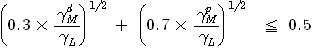
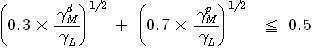
한편, 본 발명에서는 몰드의 표면특성이 열경화 타입(PDMS)에 준하는 낮은 표면에너지를 가지도록 하기 위하여 아래의 수학식 1의 조건을 만족하는 재료를 사용한다On the other hand, the present invention uses a material that satisfies the condition of the following equation 1 in order to have a low surface energy according to the thermal curing type (PDMS) of the mold surface characteristics
<수학식 1>&Quot; (1) "

여기서 γM은 몰드의 표면에너지, γL은 순수(Deionized water)의 표면에너지를 나타내며, 따라서 상기 수학식 1의 좌변(이하 '계수 A')은 몰드 표면에너지 (γM)의 분산항(dispersion term)과 극성항(polar term)에 의해 결정됨을 알 수 있다.Here, γ M represents the surface energy of the mold, γ L represents the surface energy of the deionized water, so the left side of the equation (hereinafter 'Coefficient A') is the dispersion term of the mold surface energy (γ M ) It can be seen that it is determined by the term) and the polar term.
상기 수학식 1은 아래의 과정을 통해 유도된다. Equation 1 is derived through the following process.
<수학식 2>&Quot; (2) "
![]()
![]()
<수학식 3>&Quot; (3) "
![]()
![]()
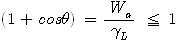
상기 수학식 2는 Young's equation 이고, 수학식 3은 Good-Girifalco의 정리(theory)이며, Wa는 점착력(Work of Adhesion) 이다. 상기 수학식 2 및 수학식 3으로부터 아래의 수학식 4가 유도된다. Equation 2 is a Young's equation, Equation 3 is a theory of Good-Girifalco, and Wa is a work of adhesion. Equation 4 below is derived from Equations 2 and 3 above.
<수학식 4>&Quot; (4) "
![]()
![]()
이때 일반적으로 물의 접촉각이 90° 이상일 때 표면이 소수성을 갖는다고 하므로, 몰드 표면이 소수성을 갖기 위해서는 다음의 수학식 5를 만족하여야 한다.In this case, since the surface is generally hydrophobic when the contact angle of water is 90 ° or more, in order to have hydrophobicity on the mold surface, the following Equation 5 must be satisfied.
<수학식 5>&Quot; (5) "
상기 수학식 5에 Owens and Wendt의 가정에 관한 아래 수학식 6을 대입하면 수학식 1이 유도된다.Substituting Equation 6 below with respect to Owens and Wendt's assumptions in Equation 5 leads to Equation 1.
<수학식 6>&Quot; (6) "
![]()
![]()
이하에서는 전술한 조건을 만족하는 광경화 타입의 몰드를 제조하는 과정을 도 2a 내지 도 2f를 참조하여 설명한다.Hereinafter, a process of manufacturing a photocuring type mold satisfying the above-described conditions will be described with reference to FIGS. 2A to 2F.
먼저, 도 2a에 도시된 바와 같이 표면에 소정의 양각 또는 음각이 형성된 마스터(20)를 준비한다. 상기 마스터(20)는 예를 들어 절연기판에 실리콘 질화막 또는 실리콘 산화막을 증착한 후에 이를 포토리소그래피 공정 등을 통해 패터닝하여 제조한다. First, as shown in FIG. 2A, a
이어서 도 2b에 도시된 바와 같이 상기 마스터(20)의 상부에 몰드레진(30)을 도포한다. Subsequently, as shown in FIG. 2B, the
상기 몰드레진(30)은 상기 수학식 1의 조건을 만족하는 재질로 이루어지며, 본 발명의 실시예에서는 몰드레진(30)이 광경화 특성을 가져야 하므로 이를 위해 몰드레진(30)이 광개시제(photo-initiator)를 함유하는 것이 바람직하다.
여기서, 몰드레진(30)은 디에틸렌글리콜 디메타크릴레이트, 에틸렌글리콜 디메타크릴레이트, 에틸렌글리콜 페닐에테르아크릴레이트, 2-에톡시-(2-에톡시)에틸아크릴레이트, 1,6-헥산디올 디아크릴레이트를 포함하는 군(群)에서 선택되는 어느 하나의 재료로 제조하거나 2이상의 물질을 혼합하여 제조함으로써, 위의 수학식 1을 만족할 수 있다. The
Here, the
삭제delete
이어서 도 2c에 도시된 바와 같이 상기 몰드레진(30)의 상부에 지지판(backplane)(50)을 부착한다. 이때 지지판(50)의 일면에 먼저 프라이머(primer)(40)를 도포한 후에 부착하는 것이 바람직하다. 경우에 따라서는 이러한 지지판(50) 부착공정은 생략될 수도 있다.Subsequently, as shown in FIG. 2C, a
지지판(50)이 부착된 다음에는 도 2d에 도시된 바와 같이, 자외선(UV)을 조사하여 몰드레진(30)을 경화시키는 광경화 과정을 거친다.After the supporting
광경화 과정은 몰드레진(30)에 함유된 광개시제에 의해 촉발되어 선형고분자 사슬의 물리적 가교반응이 활성화됨으로써 이루어진다. 본 과정은 단순히 몰드레진(30)을 경화시키기 위한 것이므로 후술하는 후처리 과정과는 목적을 달리한다.The photocuring process is triggered by the photoinitiator contained in the
몰드레진(30)이 경화된 이후에는 도 2e에 도시된 바와 같이 경화된 몰드(100)를 마스터(20)로부터 분리시킨다. 따라서 상기 몰드(100)는 마스터(20)의 양각 또는 음각에 대응하는 음각 또는 양각을 가지게 된다.After the
본 발명의 실시예에서는 몰드(100)를 마스터로부터 분리한 이후에 소수성 특성을 보다 강화하기 위하여 도 2f에 도시된 바와 같이 다시 한번 더 자외선을 조사하는 후처리과정을 거치는 점에 특징이 있다.In the embodiment of the present invention, after separating the
그리고 상기 후처리 과정에서는 자외선 강도를 2 내지 15mW/cm2 로 유지하고, 조사 시간도 10초 내지 20분 사이인 것이 바람직하다. In the post-treatment process, the ultraviolet intensity is maintained at 2 to 15 mW / cm 2 , and the irradiation time is also preferably between 10 seconds and 20 minutes.
예를 들어, 본 발명의 실시예에서 사용된 몰드에 대하여 11mW/cm2 의 강도로 5분간 자외선을 조사한 경우에, 계수 A는 0.45, 분산항은 20.8, 극성항은 2.6인 것으로 나타났다. For example, when ultraviolet rays were irradiated with an intensity of 11 mW / cm 2 for 5 minutes with respect to the mold used in the embodiment of the present invention, the coefficient A was 0.45, the dispersion term was 20.8, and the polar term was 2.6.
이러한 수치는 종래 많이 사용되는 PDMS의 물성(분산항: 18.8, 극성항: 1.6, 계수 A: 0.4)에 아주 근접한 것이며. 이로서 본 발명의 실시예에 의해 제작된 광경화 타입 소수성 몰드가 PDMS에 근접하는 소수성 특성을 가짐을 알 수 있다.These values are very close to the properties of the conventionally used PDMS (dispersion term: 18.8, polar term: 1.6, coefficient A: 0.4). As a result, it can be seen that the photocuring type hydrophobic mold prepared according to the embodiment of the present invention has hydrophobic characteristics approaching PDMS.
더욱이 본 발명의 실시예에 따른 몰드는 광경화 타입임에도 불구하고 소수성 특성이 우수할 뿐만 아니라 사용되는 재료의 점도가 PDMS에 비해 매우 낮기 때문에 수 마이크로 미터 단위의 두께를 갖는 경량박형의 몰드를 제조하는 것도 가능해진다.Furthermore, although the mold according to the embodiment of the present invention is a photocurable type, it is not only excellent in hydrophobic properties but also has a very low viscosity compared to PDMS, so that a mold having a thickness of several micrometers can be manufactured. It is also possible.
또한 열경화 타입과는 달리 몰드레진에 과도한 열이 가해지지 않기 때문에 열적 변형에 의하여 몰드 디멘죤이 당초 설계에서 벗어나는 경우도 거의 발생하지 않게 된다.In addition, unlike the thermal curing type, since excessive heat is not applied to the mold resin, the mold dimension rarely deviates from the original design due to thermal deformation.
본 발명에 따르면, 광경화 타입이면서도 열경화 타입의 PDMS와 비슷한 소수 성 특성을 가지는 몰드를 제조할 수 있다.According to the present invention, it is possible to produce a mold having a hydrophobic characteristic similar to that of a photocurable type but also a thermosetting type PDMS.
또한 점도가 낮은 재료를 사용하기 때문에 수 마이크로 미터 단위의 두께를 갖는 경량박형의 소프트 몰드를 제조하는 것이 가능해진다.Moreover, since the material with low viscosity is used, it becomes possible to manufacture the lightweight thin soft mold which has a thickness of several micrometers.
또한 광경화 타입이기 때문에 몰드레진에 과도한 열이 가해지지 않으며, 따라서 열적 변형에 의하여 몰드 디멘죤이 당초 설계에서 벗어나는 경우도 거의 발생하지 않게 된다.In addition, since the photocuring type does not apply excessive heat to the mold resin, the mold dimension almost does not occur out of the original design due to thermal deformation.
Claims (8)

Priority Applications (5)
| Application Number | Priority Date | Filing Date | Title |
|---|---|---|---|
| KR1020060057986A KR101358255B1 (en) | 2006-06-27 | 2006-06-27 | Hydrophobic mold of photo-curable type and manufacturing method for the same |
| CN2007101048597A CN101097400B (en) | 2006-06-27 | 2007-05-23 | Soft mold and method of fabricating the same |
| TW096121314A TWI398902B (en) | 2006-06-27 | 2007-06-13 | Soft mold and method of fabricating the same |
| US11/818,280 US8012667B2 (en) | 2006-06-27 | 2007-06-14 | Soft mold and method of fabricating the same |
| JP2007168248A JP4580411B2 (en) | 2006-06-27 | 2007-06-26 | Soft mold and manufacturing method thereof |
Applications Claiming Priority (1)
| Application Number | Priority Date | Filing Date | Title |
|---|---|---|---|
| KR1020060057986A KR101358255B1 (en) | 2006-06-27 | 2006-06-27 | Hydrophobic mold of photo-curable type and manufacturing method for the same |
Publications (2)
| Publication Number | Publication Date |
|---|---|
| KR20080000297A KR20080000297A (en) | 2008-01-02 |
| KR101358255B1 true KR101358255B1 (en) | 2014-02-05 |
Family
ID=39011299
Family Applications (1)
| Application Number | Title | Priority Date | Filing Date |
|---|---|---|---|
| KR1020060057986A Active KR101358255B1 (en) | 2006-06-27 | 2006-06-27 | Hydrophobic mold of photo-curable type and manufacturing method for the same |
Country Status (5)
| Country | Link |
|---|---|
| US (1) | US8012667B2 (en) |
| JP (1) | JP4580411B2 (en) |
| KR (1) | KR101358255B1 (en) |
| CN (1) | CN101097400B (en) |
| TW (1) | TWI398902B (en) |
Families Citing this family (25)
| Publication number | Priority date | Publication date | Assignee | Title |
|---|---|---|---|---|
| KR101229685B1 (en) * | 2009-08-26 | 2013-02-04 | 주식회사 엘지화학 | Pattern blancket with improved measurement stability, and method of manufacturing the same |
| SG10201506124TA (en) | 2010-08-06 | 2015-09-29 | Soken Kagaku Kk | Resin Mold For Nanoimprinting And Production Method Thereof |
| US20120070570A1 (en) * | 2010-09-16 | 2012-03-22 | Xerox Corporation | Conductive thick metal electrode forming method |
| US10543662B2 (en) | 2012-02-08 | 2020-01-28 | Corning Incorporated | Device modified substrate article and methods for making |
| US9340443B2 (en) | 2012-12-13 | 2016-05-17 | Corning Incorporated | Bulk annealing of glass sheets |
| US10014177B2 (en) | 2012-12-13 | 2018-07-03 | Corning Incorporated | Methods for processing electronic devices |
| US10086584B2 (en) | 2012-12-13 | 2018-10-02 | Corning Incorporated | Glass articles and methods for controlled bonding of glass sheets with carriers |
| TWI617437B (en) | 2012-12-13 | 2018-03-11 | 康寧公司 | Facilitated processing for controlling bonding between sheet and carrier |
| KR102060831B1 (en) | 2013-02-27 | 2019-12-30 | 삼성전자주식회사 | Flip chip packaging method, flux head using the same and flux head manufacturing method thereof |
| WO2014202127A1 (en) * | 2013-06-19 | 2014-12-24 | Ev Group E. Thallner Gmbh | Embossing compound for embossing lithography |
| US10510576B2 (en) | 2013-10-14 | 2019-12-17 | Corning Incorporated | Carrier-bonding methods and articles for semiconductor and interposer processing |
| WO2015112958A1 (en) | 2014-01-27 | 2015-07-30 | Corning Incorporated | Articles and methods for controlled bonding of thin sheets with carriers |
| JP2017518954A (en) | 2014-04-09 | 2017-07-13 | コーニング インコーポレイテッド | Substrate article modified with device and method of manufacturing the same |
| CN107073759B (en) * | 2014-11-04 | 2019-12-20 | 蓝宝迪有限公司 | Photocurable composition |
| CN107635769B (en) | 2015-05-19 | 2020-09-15 | 康宁股份有限公司 | Article and method for bonding sheet to carrier |
| CN105034344B (en) * | 2015-06-01 | 2017-09-29 | 青岛博纳光电装备有限公司 | A kind of large-area nano impressing soft mold reproducing unit and method |
| KR102524620B1 (en) | 2015-06-26 | 2023-04-21 | 코닝 인코포레이티드 | Methods and articles including sheets and carriers |
| TW201825623A (en) | 2016-08-30 | 2018-07-16 | 美商康寧公司 | Peptide plasma polymer for sheet bonding |
| TWI821867B (en) | 2016-08-31 | 2023-11-11 | 美商康寧公司 | Articles of controllably bonded sheets and methods for making same |
| CN106867442B (en) * | 2017-01-13 | 2020-09-29 | 张家港康得新光电材料有限公司 | UV curing adhesive composition, flexible mold and transfer printing method |
| KR102659516B1 (en) | 2017-08-18 | 2024-04-23 | 코닝 인코포레이티드 | glass laminate |
| CN111615567B (en) | 2017-12-15 | 2023-04-14 | 康宁股份有限公司 | Method for treating a substrate and method for producing an article comprising an adhesive sheet |
| WO2019210976A1 (en) * | 2018-05-04 | 2019-11-07 | Ev Group E. Thallner Gmbh | Stamp and method for embossing |
| JP6608997B2 (en) * | 2018-05-07 | 2019-11-20 | エーファウ・グループ・エー・タルナー・ゲーエムベーハー | Imprint materials for imprint lithography |
| KR102165655B1 (en) * | 2019-07-25 | 2020-10-14 | 서원대학교산학협력단 | Method of manufacturing patterned film and patterned film manufactured thereby |
Citations (1)
| Publication number | Priority date | Publication date | Assignee | Title |
|---|---|---|---|---|
| WO2005097449A2 (en) * | 2004-04-01 | 2005-10-20 | 3M Innovative Properties Company | Flexible mold and methods |
Family Cites Families (21)
| Publication number | Priority date | Publication date | Assignee | Title |
|---|---|---|---|---|
| US4439600A (en) * | 1983-06-03 | 1984-03-27 | Loctite Corporation | Cure to elastomers compositions |
| JP2670110B2 (en) | 1988-11-10 | 1997-10-29 | 大日本印刷株式会社 | Stamper |
| JPH08203125A (en) * | 1995-01-31 | 1996-08-09 | Pioneer Electron Corp | Laminated optical disk and its production |
| JPH09304757A (en) * | 1996-03-11 | 1997-11-28 | Sharp Corp | Liquid crystal display device and method of manufacturing the same |
| JP2001106765A (en) * | 1999-10-08 | 2001-04-17 | Dainippon Printing Co Ltd | Highly sensitive curable resin, curable resin composition, method for producing them, color filter, and liquid crystal panel |
| SE515607C2 (en) * | 1999-12-10 | 2001-09-10 | Obducat Ab | Device and method for fabrication of structures |
| US20060131784A1 (en) * | 2003-01-10 | 2006-06-22 | Takaki Sugimoto | Flexible mold, method of manufacturing same and method of manufacturing fine structures |
| JP2004281278A (en) * | 2003-03-17 | 2004-10-07 | Sony Corp | battery |
| KR100568581B1 (en) * | 2003-04-14 | 2006-04-07 | 주식회사 미뉴타텍 | Composition for micropattern forming mold and mold made therefrom |
| JP4154595B2 (en) | 2003-05-28 | 2008-09-24 | ダイキン工業株式会社 | Imprint mold and method for manufacturing the same |
| JP2007503120A (en) * | 2003-08-19 | 2007-02-15 | ナノオプト コーポレーション | Submicron scale patterning method and system |
| KR101050292B1 (en) * | 2003-12-27 | 2011-07-19 | 엘지디스플레이 주식회사 | Method of manufacturing thin film transistor array substrate |
| US7168939B2 (en) * | 2004-02-26 | 2007-01-30 | Hitachi Global Storage Technologies Netherlands Bv | System, method, and apparatus for multilevel UV molding lithography for air bearing surface patterning |
| US7401552B2 (en) * | 2004-09-16 | 2008-07-22 | Agfa Graphics N.V. | Method for manufacturing a flexographic printing master |
| US7785504B2 (en) * | 2004-11-11 | 2010-08-31 | Lg Display Co., Ltd. | Thin film patterning apparatus and method of fabricating color filter array substrate using the same |
| US7354698B2 (en) * | 2005-01-07 | 2008-04-08 | Asml Netherlands B.V. | Imprint lithography |
| KR101137862B1 (en) * | 2005-06-17 | 2012-04-20 | 엘지디스플레이 주식회사 | Fabricating method for flat display device |
| KR101212142B1 (en) * | 2005-11-28 | 2012-12-14 | 엘지디스플레이 주식회사 | Liquid Crystal Display Device And Method For Fabricating The Same |
| KR101261606B1 (en) * | 2006-05-09 | 2013-05-09 | 삼성디스플레이 주식회사 | Apparatus for manufacturing a display panel and method for manufacturing the same |
| US20080000373A1 (en) * | 2006-06-30 | 2008-01-03 | Maria Petrucci-Samija | Printing form precursor and process for preparing a stamp from the precursor |
| US7875313B2 (en) * | 2007-04-05 | 2011-01-25 | E. I. Du Pont De Nemours And Company | Method to form a pattern of functional material on a substrate using a mask material |
-
2006
- 2006-06-27 KR KR1020060057986A patent/KR101358255B1/en active Active
-
2007
- 2007-05-23 CN CN2007101048597A patent/CN101097400B/en active Active
- 2007-06-13 TW TW096121314A patent/TWI398902B/en active
- 2007-06-14 US US11/818,280 patent/US8012667B2/en active Active
- 2007-06-26 JP JP2007168248A patent/JP4580411B2/en active Active
Patent Citations (1)
| Publication number | Priority date | Publication date | Assignee | Title |
|---|---|---|---|---|
| WO2005097449A2 (en) * | 2004-04-01 | 2005-10-20 | 3M Innovative Properties Company | Flexible mold and methods |
Also Published As
| Publication number | Publication date |
|---|---|
| US8012667B2 (en) | 2011-09-06 |
| JP4580411B2 (en) | 2010-11-10 |
| KR20080000297A (en) | 2008-01-02 |
| CN101097400A (en) | 2008-01-02 |
| CN101097400B (en) | 2011-08-10 |
| TWI398902B (en) | 2013-06-11 |
| JP2008006820A (en) | 2008-01-17 |
| TW200802529A (en) | 2008-01-01 |
| US20080044743A1 (en) | 2008-02-21 |
Similar Documents
| Publication | Publication Date | Title |
|---|---|---|
| KR101358255B1 (en) | Hydrophobic mold of photo-curable type and manufacturing method for the same | |
| KR101219354B1 (en) | Polymerization technique to attenuate oxygen inhibition of solidification of liquids and composition therefor | |
| KR100568581B1 (en) | Composition for micropattern forming mold and mold made therefrom | |
| CN101923279B (en) | Nano-imprint template and preparation method thereof | |
| CN101918896B (en) | Composition for mold sheet and method for preparing mold sheet using same | |
| JP2004002702A (en) | Prepolymer material, polymer material, imprinting process and its use | |
| Lan | Soft UV nanoimprint lithography and its applications | |
| TW201038594A (en) | Curable composition for nanoimprint and cured product | |
| Chen et al. | High density patterns fabricated in SU-8 by UV curing nanoimprint | |
| CN101078880B (en) | Composition for forming pattern and in-plane printing method using the same | |
| del Campo et al. | Generating micro-and nanopatterns on polymeric materials | |
| KR100832298B1 (en) | Pattern forming resist and soft mold manufacturing method using the same | |
| JP2012204429A (en) | Template for imprint, manufacturing method of the template, and pattern formation method of the template | |
| KR100848559B1 (en) | Soft Mold Manufacturing Method and Pattern Forming Method Using the Same | |
| Youn et al. | Microstructuring of SU-8 photoresist by UV-assisted thermal imprinting with non-transparent mold | |
| CN112470254B (en) | Method for producing molded article, resist for co-molding for imprint-electron lithography, method for producing replica mold, method for producing apparatus, and imprint material | |
| KR101284943B1 (en) | Method for fabricating mold | |
| KR20080097499A (en) | Imprints and Manufacturing Methods | |
| Rodríguez et al. | Soft thermal nanoimprint and hybrid processes to produce complex structures | |
| KR20130010583A (en) | Photocurable resin composition | |
| TWI389931B (en) | Nano-imprint resist and nanoimprinting lithography method using the same | |
| CN113169045A (en) | Method for forming fine pattern, method for manufacturing imprint mold, and optical device | |
| Kang et al. | Portable UV nanoimprint lithography system using hydraulic pressure | |
| JP2012061599A (en) | Application of benzocyclobutene resin to imprint technology, and method for forming pattern by the technology | |
| KR20080098212A (en) | Lithography Methods Combining Photolithography and Nanoimprint Lithography |
Legal Events
| Date | Code | Title | Description |
|---|---|---|---|
| PA0109 | Patent application |
St.27 status event code: A-0-1-A10-A12-nap-PA0109 |
|
| PG1501 | Laying open of application |
St.27 status event code: A-1-1-Q10-Q12-nap-PG1501 |
|
| PN2301 | Change of applicant |
St.27 status event code: A-3-3-R10-R13-asn-PN2301 St.27 status event code: A-3-3-R10-R11-asn-PN2301 |
|
| R18-X000 | Changes to party contact information recorded |
St.27 status event code: A-3-3-R10-R18-oth-X000 |
|
| A201 | Request for examination | ||
| PA0201 | Request for examination |
St.27 status event code: A-1-2-D10-D11-exm-PA0201 |
|
| R18-X000 | Changes to party contact information recorded |
St.27 status event code: A-3-3-R10-R18-oth-X000 |
|
| R18-X000 | Changes to party contact information recorded |
St.27 status event code: A-3-3-R10-R18-oth-X000 |
|
| E902 | Notification of reason for refusal | ||
| PE0902 | Notice of grounds for rejection |
St.27 status event code: A-1-2-D10-D21-exm-PE0902 |
|
| AMND | Amendment | ||
| E13-X000 | Pre-grant limitation requested |
St.27 status event code: A-2-3-E10-E13-lim-X000 |
|
| P11-X000 | Amendment of application requested |
St.27 status event code: A-2-2-P10-P11-nap-X000 |
|
| P13-X000 | Application amended |
St.27 status event code: A-2-2-P10-P13-nap-X000 |
|
| E601 | Decision to refuse application | ||
| PE0601 | Decision on rejection of patent |
St.27 status event code: N-2-6-B10-B15-exm-PE0601 |
|
| AMND | Amendment | ||
| J201 | Request for trial against refusal decision | ||
| P11-X000 | Amendment of application requested |
St.27 status event code: A-2-2-P10-P11-nap-X000 |
|
| P13-X000 | Application amended |
St.27 status event code: A-2-2-P10-P13-nap-X000 |
|
| PJ0201 | Trial against decision of rejection |
St.27 status event code: A-3-3-V10-V11-apl-PJ0201 |
|
| PB0901 | Examination by re-examination before a trial |
St.27 status event code: A-6-3-E10-E12-rex-PB0901 |
|
| E90F | Notification of reason for final refusal | ||
| PE0902 | Notice of grounds for rejection |
St.27 status event code: A-1-2-D10-D21-exm-PE0902 |
|
| P11-X000 | Amendment of application requested |
St.27 status event code: A-2-2-P10-P11-nap-X000 |
|
| P13-X000 | Application amended |
St.27 status event code: A-2-2-P10-P13-nap-X000 |
|
| B701 | Decision to grant | ||
| PB0701 | Decision of registration after re-examination before a trial |
St.27 status event code: A-3-4-F10-F13-rex-PB0701 |
|
| GRNT | Written decision to grant | ||
| PR0701 | Registration of establishment |
St.27 status event code: A-2-4-F10-F11-exm-PR0701 |
|
| PR1002 | Payment of registration fee |
St.27 status event code: A-2-2-U10-U11-oth-PR1002 Fee payment year number: 1 |
|
| PG1601 | Publication of registration |
St.27 status event code: A-4-4-Q10-Q13-nap-PG1601 |
|
| FPAY | Annual fee payment |
Payment date: 20161214 Year of fee payment: 4 |
|
| PR1001 | Payment of annual fee |
St.27 status event code: A-4-4-U10-U11-oth-PR1001 Fee payment year number: 4 |
|
| FPAY | Annual fee payment |
Payment date: 20171218 Year of fee payment: 5 |
|
| PR1001 | Payment of annual fee |
St.27 status event code: A-4-4-U10-U11-oth-PR1001 Fee payment year number: 5 |
|
| FPAY | Annual fee payment |
Payment date: 20181226 Year of fee payment: 6 |
|
| PR1001 | Payment of annual fee |
St.27 status event code: A-4-4-U10-U11-oth-PR1001 Fee payment year number: 6 |
|
| FPAY | Annual fee payment |
Payment date: 20191212 Year of fee payment: 7 |
|
| PR1001 | Payment of annual fee |
St.27 status event code: A-4-4-U10-U11-oth-PR1001 Fee payment year number: 7 |
|
| PR1001 | Payment of annual fee |
St.27 status event code: A-4-4-U10-U11-oth-PR1001 Fee payment year number: 8 |
|
| PR1001 | Payment of annual fee |
St.27 status event code: A-4-4-U10-U11-oth-PR1001 Fee payment year number: 9 |
|
| PR1001 | Payment of annual fee |
St.27 status event code: A-4-4-U10-U11-oth-PR1001 Fee payment year number: 10 |
|
| PR1001 | Payment of annual fee |
St.27 status event code: A-4-4-U10-U11-oth-PR1001 Fee payment year number: 11 |
|
| PR1001 | Payment of annual fee |
St.27 status event code: A-4-4-U10-U11-oth-PR1001 Fee payment year number: 12 |
|
| PN2301 | Change of applicant |
St.27 status event code: A-5-5-R10-R11-asn-PN2301 |
|
| PN2301 | Change of applicant |
St.27 status event code: A-5-5-R10-R14-asn-PN2301 |
|
| PR1001 | Payment of annual fee |
St.27 status event code: A-4-4-U10-U11-oth-PR1001 Fee payment year number: 13 |
|
| U11 | Full renewal or maintenance fee paid |
Free format text: ST27 STATUS EVENT CODE: A-4-4-U10-U11-OTH-PR1001 (AS PROVIDED BY THE NATIONAL OFFICE) Year of fee payment: 13 |