BR112014011800B1 - bipolar electrostatic transfer head - Google Patents
bipolar electrostatic transfer head Download PDFInfo
- Publication number
- BR112014011800B1 BR112014011800B1 BR112014011800-0A BR112014011800A BR112014011800B1 BR 112014011800 B1 BR112014011800 B1 BR 112014011800B1 BR 112014011800 A BR112014011800 A BR 112014011800A BR 112014011800 B1 BR112014011800 B1 BR 112014011800B1
- Authority
- BR
- Brazil
- Prior art keywords
- transfer head
- microdevice
- electrode
- electrostatic transfer
- table structure
- Prior art date
Links
Images


Classifications
-
- H10P72/722—
-
- H—ELECTRICITY
- H10—SEMICONDUCTOR DEVICES; ELECTRIC SOLID-STATE DEVICES NOT OTHERWISE PROVIDED FOR
- H10D—INORGANIC ELECTRIC SEMICONDUCTOR DEVICES
- H10D62/00—Semiconductor bodies, or regions thereof, of devices having potential barriers
- H10D62/10—Shapes, relative sizes or dispositions of the regions of the semiconductor bodies; Shapes of the semiconductor bodies
- H10D62/117—Shapes of semiconductor bodies
-
- H10P72/0446—
-
- B—PERFORMING OPERATIONS; TRANSPORTING
- B32—LAYERED PRODUCTS
- B32B—LAYERED PRODUCTS, i.e. PRODUCTS BUILT-UP OF STRATA OF FLAT OR NON-FLAT, e.g. CELLULAR OR HONEYCOMB, FORM
- B32B2457/00—Electrical equipment
- B32B2457/20—Displays, e.g. liquid crystal displays, plasma displays
-
- B—PERFORMING OPERATIONS; TRANSPORTING
- B32—LAYERED PRODUCTS
- B32B—LAYERED PRODUCTS, i.e. PRODUCTS BUILT-UP OF STRATA OF FLAT OR NON-FLAT, e.g. CELLULAR OR HONEYCOMB, FORM
- B32B37/00—Methods or apparatus for laminating, e.g. by curing or by ultrasonic bonding
- B32B37/02—Methods or apparatus for laminating, e.g. by curing or by ultrasonic bonding characterised by a sequence of laminating steps, e.g. by adding new layers at consecutive laminating stations
- B32B37/025—Transfer laminating
-
- B—PERFORMING OPERATIONS; TRANSPORTING
- B32—LAYERED PRODUCTS
- B32B—LAYERED PRODUCTS, i.e. PRODUCTS BUILT-UP OF STRATA OF FLAT OR NON-FLAT, e.g. CELLULAR OR HONEYCOMB, FORM
- B32B37/00—Methods or apparatus for laminating, e.g. by curing or by ultrasonic bonding
- B32B37/06—Methods or apparatus for laminating, e.g. by curing or by ultrasonic bonding characterised by the heating method
-
- H10W70/682—
-
- H10W72/0198—
-
- H10W72/0711—
-
- H10W72/07178—
-
- H10W72/07307—
-
- Y—GENERAL TAGGING OF NEW TECHNOLOGICAL DEVELOPMENTS; GENERAL TAGGING OF CROSS-SECTIONAL TECHNOLOGIES SPANNING OVER SEVERAL SECTIONS OF THE IPC; TECHNICAL SUBJECTS COVERED BY FORMER USPC CROSS-REFERENCE ART COLLECTIONS [XRACs] AND DIGESTS
- Y10—TECHNICAL SUBJECTS COVERED BY FORMER USPC
- Y10T—TECHNICAL SUBJECTS COVERED BY FORMER US CLASSIFICATION
- Y10T156/00—Adhesive bonding and miscellaneous chemical manufacture
- Y10T156/11—Methods of delaminating, per se; i.e., separating at bonding face
- Y10T156/1153—Temperature change for delamination [e.g., heating during delaminating, etc.]
-
- Y—GENERAL TAGGING OF NEW TECHNOLOGICAL DEVELOPMENTS; GENERAL TAGGING OF CROSS-SECTIONAL TECHNOLOGIES SPANNING OVER SEVERAL SECTIONS OF THE IPC; TECHNICAL SUBJECTS COVERED BY FORMER USPC CROSS-REFERENCE ART COLLECTIONS [XRACs] AND DIGESTS
- Y10—TECHNICAL SUBJECTS COVERED BY FORMER USPC
- Y10T—TECHNICAL SUBJECTS COVERED BY FORMER US CLASSIFICATION
- Y10T156/00—Adhesive bonding and miscellaneous chemical manufacture
- Y10T156/17—Surface bonding means and/or assemblymeans with work feeding or handling means
- Y10T156/1702—For plural parts or plural areas of single part
- Y10T156/1705—Lamina transferred to base from adhered flexible web or sheet type carrier
- Y10T156/1707—Discrete spaced laminae on adhered carrier
-
- Y—GENERAL TAGGING OF NEW TECHNOLOGICAL DEVELOPMENTS; GENERAL TAGGING OF CROSS-SECTIONAL TECHNOLOGIES SPANNING OVER SEVERAL SECTIONS OF THE IPC; TECHNICAL SUBJECTS COVERED BY FORMER USPC CROSS-REFERENCE ART COLLECTIONS [XRACs] AND DIGESTS
- Y10—TECHNICAL SUBJECTS COVERED BY FORMER USPC
- Y10T—TECHNICAL SUBJECTS COVERED BY FORMER US CLASSIFICATION
- Y10T156/00—Adhesive bonding and miscellaneous chemical manufacture
- Y10T156/17—Surface bonding means and/or assemblymeans with work feeding or handling means
- Y10T156/1702—For plural parts or plural areas of single part
- Y10T156/1744—Means bringing discrete articles into assembled relationship
- Y10T156/1749—All articles from single source only
-
- Y—GENERAL TAGGING OF NEW TECHNOLOGICAL DEVELOPMENTS; GENERAL TAGGING OF CROSS-SECTIONAL TECHNOLOGIES SPANNING OVER SEVERAL SECTIONS OF THE IPC; TECHNICAL SUBJECTS COVERED BY FORMER USPC CROSS-REFERENCE ART COLLECTIONS [XRACs] AND DIGESTS
- Y10—TECHNICAL SUBJECTS COVERED BY FORMER USPC
- Y10T—TECHNICAL SUBJECTS COVERED BY FORMER US CLASSIFICATION
- Y10T156/00—Adhesive bonding and miscellaneous chemical manufacture
- Y10T156/17—Surface bonding means and/or assemblymeans with work feeding or handling means
- Y10T156/1702—For plural parts or plural areas of single part
- Y10T156/1744—Means bringing discrete articles into assembled relationship
- Y10T156/1776—Means separating articles from bulk source
Landscapes
- Micromachines (AREA)
- Container, Conveyance, Adherence, Positioning, Of Wafer (AREA)
- Engineering & Computer Science (AREA)
- Led Device Packages (AREA)
- Computer Hardware Design (AREA)
- Electrodes Of Semiconductors (AREA)
- Power Engineering (AREA)
- Printers Or Recording Devices Using Electromagnetic And Radiation Means (AREA)
- Microelectronics & Electronic Packaging (AREA)
- Manufacturing & Machinery (AREA)
- Die Bonding (AREA)
- Wire Bonding (AREA)
- Bipolar Transistors (AREA)
- Physics & Mathematics (AREA)
- Condensed Matter Physics & Semiconductors (AREA)
- General Physics & Mathematics (AREA)
- Automatic Analysis And Handling Materials Therefor (AREA)
Abstract
cabeça de transferência de microdispositivo. trata-se de uma cabeça de transferência de microdispositivo e um arranjo de cabeça que são revelados. em uma modalidade, a cabeça de transferência de microdispositivo inclui um substrato base, uma estrutura de mesa com paredes laterais, um eletrodo formado sobre a estrutura de mesa, e uma camada dielétrica que cobre o eletrodo. uma tensão pode ser aplicada à cabeça de transferência de microdispositivo e arranjo de cabeça para pegar um microdispositivo de um substrato de carreador e liberar o microdispositivo em um substrato de recepção.microdevice transfer head. it is a microdevice transfer head and a head arrangement that are revealed. in one embodiment, the microdevice transfer head includes a base substrate, a table structure with side walls, an electrode formed on the table structure, and a dielectric layer that covers the electrode. a tension can be applied to the microdevice transfer head and head arrangement to take a microdevice from a carrier substrate and release the microdevice on a receiving substrate.
Description
[0001] Este pedido reivindica o benefício da prioridade do pedido de patente provisório n° de série US 61/561.706 depositado em 18 de novembro de 2011, pedido de patente provisório n° de série US 61/594.919 depositado em 3 de fevereiro de 2012 e pedido de patente provisório n° US de série 61/597.109 depositado em 9 de fevereiro de 2012, as revelações completas das quais estão aqui no presente documento incorporadas a título de referência.[0001] This application claims priority benefit from provisional patent application serial number US 61 / 561,706 filed on November 18, 2011, provisional patent application serial number US 61 / 594,919 filed on February 3, 2012 and provisional patent application No. US series 61 / 597,109 filed on February 9, 2012, the full disclosures of which are hereby incorporated by reference.
[0002] A presente invenção se refere a microdispositivos. Mais particularmente, as modalidades da presente invenção se referem a uma cabeça de transferência de microdispositivo e um método de transferência de um ou mais microdispositivos para um substrato de recepção.[0002] The present invention relates to microdevices. More particularly, the embodiments of the present invention relate to a microdevice transfer head and a method of transferring one or more microdevices to a receiving substrate.
[0003] As questões de integração e de embalamento são um dos principais obstáculos para a comercialização de microdispositivos como, por exemplo, micro chaves de sistemas micro eletromecânicos (MEMS) de frequência de rádio (RF), sistemas de exibição de diodo emissor de luz (LED) e osciladores com base em MEMS ou quartzo.[0003] Integration and packaging issues are one of the main obstacles to the commercialization of microdevices, for example, micro-keys of radio frequency micro-electromechanical (MEMS) systems, LED display systems (LED) and oscillators based on MEMS or quartz.
[0004] As tecnologias tradicionais para a transferência de dispositivos incluem a transferência através de ligação de pastilha de uma pastilha de transferência para uma pastilha de recepção. Tal implantação é "impressão direta" que envolve uma etapa de ligação de um arranjo de dispositivos de uma pastilha de transferência para uma pastilha de recepção, seguido da remoção da pastilha de transferência. Uma outra tal implantação é "impressão de transferência"que envolve duas etapas de ligação/desligamento. Na impressão de transferência uma pastilha de transferência pode pegar um arranjo de dispositivos de uma pastilha doadora e, então, ligar o arranjo dos dispositivos para uma pastilha de recepção, seguido da remoção da pastilha de transferência.[0004] Traditional technologies for transferring devices include transferring through tablet connection from a transferring tablet to a receiving tablet. Such an implantation is "direct printing" which involves a step of connecting an arrangement of devices from a transfer pad to a receiving pad, followed by removal of the transfer pad. Another such deployment is "transfer printing" which involves two steps of switching on / off. In transfer printing a transfer insert can take an arrangement of devices from a donor insert and then connect the arrangement of the devices to a receiving insert, followed by removal of the transfer insert.
[0005] Algumas variações do processo de impressão foram desenvolvidas em que um dispositivo pode ser seletivamente ligado e desligado durante o processo de transferência. Em ambas aas tecnologias tradicionais e variações da impressão direta e da impressão de transferência, a pastilha de transferência é desligada de um dispositivo após ligar o dispositivo à pastilha de recepção. Além disso, toda a pastilha de transferência com o arranjo de dispositivos é envolvida no processo de transferência.[0005] Some variations of the printing process have been developed in which a device can be selectively turned on and off during the transfer process. In both traditional technologies and variations of direct printing and transfer printing, the transfer pad is disconnected from a device after connecting the device to the receiving pad. In addition, the entire transfer pad with the device arrangement is involved in the transfer process.
[0006] Uma cabeça e um arranjo de cabeças de transferência de microdispositivo e um método de transferência de um ou mais microdispositivos para um substrato de recepção são revelados. Por exemplo, o substrato de recepção pode ser, mas não se limita a, um substrato de exibição, um substrato de iluminação, um substrato com os dispositivos funcionais como, por exemplo, transistores ou circuitos integrados (ICs) ou um substrato com linhas de redistribuição de metal.[0006] A head and array of microdevice transfer heads and a method of transferring one or more microdevices to a receiving substrate are disclosed. For example, the receiving substrate can be, but is not limited to, a display substrate, a lighting substrate, a substrate with functional devices such as transistors or integrated circuits (ICs) or a substrate with lines of metal redistribution.
[0007] Em uma modalidade, uma cabeça de transferência de microdispositivo inclui um substrato de base, uma estrutura de mesa que inclui paredes laterais, pelo menos um é o eletrodo formado sobre a estrutura de mesa e uma camada dielétrica que cobre o eletrodo. Por exemplo, a cabeça de transferência de microdispositivo pode incorporar uma estrutura de eletrodo monopolar ou bipolar. A estrutura de mesa pode ser separada ou integralmente formadas com o substrato de base As paredes laterais podem ser afuniladas e projetadas na direção contrária do substrato de base para uma superfície de topo da estrutura de mesa, com o eletrodo formado na superfície de topo. Um condutor de eletrodo pode se estender do eletrodo a fim de fazer contato com a fiação no substrato de base e conectar a cabeça de transferência de microdispositivo aos componentes eletrônicos em funcionamento de um conjunto de pegador eletrostático. Os condutores de eletrodo podem percorrer do eletrodo na superfície de topo da estrutura de mesa e ao longo de uma parede lateral da estrutura de mesa. O condutor de eletrodo pode alternativamente correr abaixo da estrutura de mesa e se conectar uma via que correr através da estrutura de mesa ao eletrodo.[0007] In one embodiment, a microdevice transfer head includes a base substrate, a table structure that includes side walls, at least one is the electrode formed on the table structure and a dielectric layer that covers the electrode. For example, the microdevice transfer head can incorporate a monopolar or bipolar electrode structure. The table structure can be separated or integrally formed with the base substrate. The side walls can be tapered and projected in the opposite direction from the base substrate to a top surface of the table structure, with the electrode formed on the top surface. An electrode conductor can extend from the electrode in order to make contact with the wiring in the base substrate and connect the microdevice transfer head to the operating electronic components of an electrostatic holder assembly. The electrode conductors can run through the electrode on the top surface of the table structure and along a side wall of the table structure. The electrode conductor can alternatively run below the table structure and connect a path that runs through the table structure to the electrode.
[0008] O eletrodo e os condutores de eletrodo podem ser cobertos com uma camada dielétrica depositada. Os materiais adequados para a camada dielétrica incluem, mas não se limitam a, a óxido de alumínio (Al2O3) e a óxido de tântalo (Ta2O5). Uma vez que a camada dielétrica é disposta, o eletrodo e os condutores de eletrodo podem ser formados de um material que pode suportar as altas temperaturas de deposição, o que inclui metais de alta temperatura de fusão como, por exemplo, platina e metais refratários ou ligas de metal refratário como, por exemplo, tungstênio titânio (TiW).[0008] The electrode and electrode conductors can be covered with a deposited dielectric layer. Suitable materials for the dielectric layer include, but are not limited to, aluminum oxide (Al2O3) and tantalum oxide (Ta2O5). Once the dielectric layer is laid out, the electrode and electrode conductors can be formed of a material that can withstand high deposition temperatures, which includes high-melting metals such as platinum and refractory metals or refractory metal alloys such as titanium tungsten (TiW).
[0009] Em uma modalidade, um método de transferência de um microdispositivo inclui posicionar uma cabeça de transferência sobre um microdispositivo conectado a um substrato portador. O microdispositivo é colocado em contato com a cabeça de transferência e uma tensão é aplicada a um eletrodo na cabeça de transferência para criar uma pressão de pega no microdispositivo. A cabeça de transferência pega o microdispositivo e, então, libera o microdispositivo em um substrato de recepção. A tensão pode ser aplicada ao eletrodo anterior ao, enquanto ou após contato com o microdispositivo com a cabeça de transferência. A tensão pode ser uma tensão de corrente constante ou tensão de corrente alternada. Em uma modalidade, uma tensão de corrente alternada é aplicada a uma estrutura de eletrodo bipolar. Em uma modalidade, uma operação é ainda realizada para criar uma alteração de fase em uma camada de ligação que conecta o microdispositivo ao substrato portador anterior a ou enquanto pega o microdispositivo.[0009] In one embodiment, a method of transferring a microdevice includes placing a transfer head on a microdevice connected to a carrier substrate. The microdevice is placed in contact with the transfer head and a voltage is applied to an electrode on the transfer head to create a grip pressure on the microdevice. The transfer head picks up the microdevice and then releases the microdevice on a receiving substrate. The voltage can be applied to the electrode prior to, while or after contacting the microdevice with the transfer head. The voltage can be a constant current voltage or alternating current voltage. In one embodiment, an alternating current voltage is applied to a bipolar electrode structure. In one embodiment, an operation is still performed to create a phase change in a bonding layer that connects the microdevice to the carrier substrate prior to or while picking up the microdevice.
[0010] Em uma modalidade, a camada de ligação é aquecida para criar uma alteração de fase de sólido para líquido na camada de ligação anterior a ou enquanto pega um microdispositivo. Dependendo das condições de operação, uma porção substancial da camada de ligação pode ser segurada e transferida com o microdispositivo. Uma variedade de operações pode ser realizada para controlar a fase da porção da camada de ligação quando se pega, transfere, entra em contato com o substrato de recepção e que libera o microdispositivo e a porção da camada de ligação no substrato de recepção. Por exemplo, a porção da camada de ligação que é segurada com o microdispositivo pode ser mantida no estado líquido quando em contato com o substrato de recepção e durante a operação de liberação no substrato de recepção. Em uma outra modalidade, a porção da camada de ligação pode ser deixada para resfriar naturalmente para uma fase sólida após ser segurada. Por exemplo, a porção da camada de ligação pode estar em uma fase sólida anterior a ou durante o contato com o substrato de recepção e, novamente, fundido para o estado líquido durante a operação de liberação. Uma variedade de ciclos de temperatura e de fase de material pode ser realizada de acordo com as modalidades da invenção.[0010] In one embodiment, the bonding layer is heated to create a phase change from solid to liquid in the bonding layer prior to or while picking up a microdevice. Depending on the operating conditions, a substantial portion of the bonding layer can be held and transferred with the microdevice. A variety of operations can be performed to control the phase of the bonding layer portion when picking, transferring, contacting the receiving substrate and releasing the microdevice and the bonding layer portion on the receiving substrate. For example, the portion of the bonding layer that is held with the microdevice can be kept in a liquid state when in contact with the receiving substrate and during the release operation on the receiving substrate. In another embodiment, the portion of the bonding layer can be left to naturally cool to a solid phase after being held. For example, the portion of the bonding layer may be in a solid phase prior to or during contact with the receiving substrate and again fused to a liquid state during the release operation. A variety of temperature and material phase cycles can be performed according to the modalities of the invention.
[0011] Em uma modalidade, um método de transferência de um arranjo de microdispositivos inclui posicionar um arranjo de cabeças de transferência sobre um arranjo de microdispositivos. O arranjo de microdispositivos é colocado em contato com o arranjo de cabeças de transferência e uma tensão é seletivamente aplicada a uma porção do arranjo de cabeças de transferência. A aplicação de modo seletivo de uma tensão pode incluir aplicar uma tensão a todas das cabeças de transferência no arranjo ou a uma porção que corresponde a menos que todas das cabeças de transferência no arranjo. A porção correspondente do arranjo de microdispositivos é, então, pegada com a porção do arranjo de cabeças de transferência e a porção do arranjo de microdispositivos é liberada de modo seletivo em pelo menos um substrato de recepção. Em uma modalidade, o arranjo de cabeças de transferência pode ser esfregado no arranjo de microdispositivos enquanto faz contato a fim de desalojar quaisquer partículas que possam estar presentes na superfície de contato de qualquer uma das cabeças de transferência ou microdispositivos. Em uma modalidade, uma alteração de fase é criada em um arranjo de locais lateralmente separados da camada de ligação que conectam o arranjo de microdispositivos ao substrato portador anterior a pegada do arranjo de microdispositivos.[0011] In one embodiment, a method of transferring an array of microdevices includes positioning an array of transfer heads on an array of microdevices. The array of microdevices is brought into contact with the array of transfer heads and a voltage is selectively applied to a portion of the array of transfer heads. Selectively applying a voltage can include applying a voltage to all of the transfer heads in the array or to a portion that corresponds to less than all of the transfer heads in the array. The corresponding portion of the microdevice array is then taken with the transfer head array portion and the microdevice array portion is selectively released on at least one receiving substrate. In one embodiment, the arrangement of transfer heads can be rubbed into the arrangement of microdevices while making contact in order to dislodge any particles that may be present on the contact surface of any of the transfer heads or microdevices. In one embodiment, a phase change is created in an arrangement of locations laterally separate from the bonding layer that connect the array of microdevices to the carrier substrate prior to the footprint of the array of microdevices.
[0012] Em uma modalidade, um método de fabricação de uma cabeça de transferência de microdispositivo arranjo inclui formar um arranjo de estruturas de mesa em um substrato de base, com cada estrutura de mesa que inclui paredes laterais. Um eletrodo separado é formado sobre cada estrutura de mesa e uma camada dielétrica é disposta sobre o arranjo de estruturas de mesa e cada eletrodo. Em uma modalidade, a camada dielétrica é disposta com a deposição de camada atômica (ALD) e pode ser livre de micro -orifício. A camada dielétrica pode incluir uma ou múltiplas camadas dielétricas. Uma camada de passivação conformal pode, opcionalmente, ser cultivada ou depositada sobre o substrato de base e o arranjo de estruturas de mesa anterior a formação do eletrodo separado sobre cada estrutura de mesa correspondente. Em uma modalidade, um plano de terra condutivo é formado sobre a camada dielétrica e circunda cada uma das estruturas de mesa.[0012] In one embodiment, a method of fabricating a microdevice transfer head arrangement includes forming an arrangement of table structures on a base substrate, with each table structure including side walls. A separate electrode is formed over each table structure and a dielectric layer is placed over the arrangement of table structures and each electrode. In one embodiment, the dielectric layer is arranged with the deposition of the atomic layer (ALD) and can be free of micro-orifice. The dielectric layer can include one or multiple dielectric layers. A conformal passivation layer can optionally be cultivated or deposited on the base substrate and the arrangement of table structures prior to the formation of the separate electrode on each corresponding table structure. In one embodiment, a conductive ground plane is formed over the dielectric layer and surrounds each of the table structures.
[0013] A Figura 1 é uma ilustração da vista lateral em corte transversal de uma cabeça de transferência de microdispositivo monopolar de acordo com uma modalidade da invenção.[0013] Figure 1 is a cross-sectional side view of a monopolar microdevice transfer head according to an embodiment of the invention.
[0014] A Figura 2 é uma ilustração de vista isométrica de um monopolar cabeça de transferência de microdispositivo de acordo com uma modalidade da invenção.[0014] Figure 2 is an isometric view illustration of a monopolar microdevice transfer head according to an embodiment of the invention.
[0015] A Figura 3 é uma ilustração de vista lateral em corte transversal de uma cabeça de transferência de microdispositivo bipolar de acordo com uma modalidade da invenção.[0015] Figure 3 is a side view illustration in cross-section of a bipolar microdevice transfer head according to an embodiment of the invention.
[0016] A Figura 4 é uma ilustração de vista isométrica de uma cabeça de transferência de microdispositivo bipolar de acordo com uma modalidade da invenção.[0016] Figure 4 is an isometric view illustration of a bipolar microdevice transfer head according to an embodiment of the invention.
[0017] As Figuras 5 a 6 são ilustrações de vista de topo de uma cabeça de transferência de microdispositivo bipolar de acordo com uma modalidade da invenção.[0017] Figures 5 to 6 are top view illustrations of a bipolar microdevice transfer head according to an embodiment of the invention.
[0018] A Figura 7 é uma ilustração de vista isométrica de uma cabeça de transferência de microdispositivo bipolar que inclui vias condutivas de acordo com uma modalidade da invenção.[0018] Figure 7 is an isometric view illustration of a bipolar microdevice transfer head that includes conductive pathways according to an embodiment of the invention.
[0019] A Figura 8 é uma ilustração de vista isométrica de um arranjo de cabeça de transferência de microdispositivo bipolar de acordo com uma modalidade da invenção.[0019] Figure 8 is an isometric view illustration of a bipolar microdevice transfer head arrangement according to an embodiment of the invention.
[0020] A Figura 9 é uma ilustração de vista isométrica de um arranjo de cabeça de transferência de microdispositivo bipolar que inclui um plano de terra condutivo de acordo com uma modalidade da invenção.[0020] Figure 9 is an isometric view illustration of a bipolar microdevice transfer head arrangement that includes a conductive ground plane according to an embodiment of the invention.
[0021] A Figura 10 é uma ilustração de vista lateral em corte transversal de um arranjo de cabeça de transferência de microdispositivo bipolar que inclui um plano de terra condutivo de acordo com uma modalidade da invenção.[0021] Figure 10 is a side view illustration in cross section of a bipolar microdevice transfer head arrangement that includes a conductive ground plane according to an embodiment of the invention.
[0022] A Figura 11 é um fluxograma que ilustra um método de pegar e transferir um microdispositivo de um substrato portador para um substrato de recepção de acordo com uma modalidade da invenção.[0022] Figure 11 is a flow chart illustrating a method of picking up and transferring a microdevice from a carrier substrate to a receiving substrate according to an embodiment of the invention.
[0023] A Figura 12 é uma ilustração esquemática de uma tensão alternante aplicada através de um eletrodo bipolar de acordo com uma modalidade da invenção.[0023] Figure 12 is a schematic illustration of an alternating voltage applied through a bipolar electrode according to an embodiment of the invention.
[0024] A Figura 13 é uma ilustração esquemática de uma tensão constante aplicada através de um eletrodo bipolar de acordo com uma modalidade da invenção.[0024] Figure 13 is a schematic illustration of a constant voltage applied through a bipolar electrode according to an embodiment of the invention.
[0025] A Figura 14 é uma ilustração esquemática de uma tensão constante aplicada a um eletrodo monopolar de acordo com uma modalidade da invenção.[0025] Figure 14 is a schematic illustration of a constant voltage applied to a monopolar electrode according to an embodiment of the invention.
[0026] A Figura 15 é um fluxograma que ilustra um método de pegar e transferir um microdispositivo de um substrato portador para um substrato de recepção de acordo com uma modalidade da invenção.[0026] Figure 15 is a flow chart illustrating a method of picking up and transferring a microdevice from a carrier substrate to a receiving substrate according to an embodiment of the invention.
[0027] A Figura 16 é um fluxograma que ilustra um método de pegar e transferir um arranjo de microdispositivos de um substrato portador para pelo menos um substrato de recepção de acordo com uma modalidade da invenção.[0027] Figure 16 is a flow chart illustrating a method of picking up and transferring an array of microdevices from a carrier substrate to at least one receiving substrate according to one embodiment of the invention.
[0028] A Figura 17 é uma ilustração de vista lateral em corte transversal de um arranjo de cabeça de transferência de microdispositivos em contato com um arranjo de microdispositivos de LED de acordo com uma modalidade da invenção.[0028] Figure 17 is a cross-sectional side view illustration of a microdevice transfer head arrangement in contact with an LED microdevice arrangement according to an embodiment of the invention.
[0029] A Figura 18 é uma ilustração de vista lateral em corte transversal de um arranjo de cabeça de transferência de microdispositivos em contato com um arranjo de microdispositivos de LED de acordo com uma modalidade da invenção.[0029] Figure 18 is a side view illustration in cross section of a microdevice transfer head arrangement in contact with an LED microdevice arrangement according to an embodiment of the invention.
[0030] A Figura 19 é uma ilustração de vista lateral em corte transversal de um arranjo de cabeça de transferência de microdispositivos que pega um arranjo de microdispositivos de LED de acordo com uma modalidade da invenção.[0030] Figure 19 is a side view illustration in cross section of a microdevice transfer head arrangement that takes an LED microdevice arrangement according to an embodiment of the invention.
[0031] A Figura 20 é uma ilustração de vista lateral em corte transversal de um arranjo de cabeça de transferência de microdispositivos que pega uma porção de um arranjo de microdispositivos de LED de acordo com uma modalidade da invenção.[0031] Figure 20 is a cross-sectional side view illustration of a microdevice transfer head arrangement that takes a portion of an LED microdevice arrangement according to an embodiment of the invention.
[0032] A Figura 21 é uma ilustração de vista lateral em corte transversal de um arranjo de cabeça de transferência de microdispositivos com um arranjo de microdispositivos de LED posicionado sobre um substrato de recepção de acordo com uma modalidade da invenção.[0032] Figure 21 is a cross-sectional side view illustration of a microdevice transfer head arrangement with an LED microdevice arrangement positioned on a receiving substrate according to an embodiment of the invention.
[0033] A Figura 22 é uma ilustração de vista lateral em corte transversal de um microdispositivo liberado de modo seletivo em um substrato de recepção de acordo com uma modalidade da invenção.[0033] Figure 22 is a side view illustration in cross section of a microdevice released selectively on a receiving substrate according to an embodiment of the invention.
[0034] A Figura 23 é uma ilustração gráfica que mostra a pressão exigida para superar a força da tensão superficial para pegar um microdispositivo de várias dimensões de acordo com uma modalidade da invenção.[0034] Figure 23 is a graphic illustration showing the pressure required to overcome the force of surface tension to pick up a microdevice of various dimensions according to one embodiment of the invention.
[0035] A Figura 24 é uma ilustração gráfica da relação entre uma tensão de superfície e a crescente distância de vão criada durante uma operação de pegar de acordo com uma modalidade da invenção.[0035] Figure 24 is a graphic illustration of the relationship between a surface tension and the increasing span distance created during a gripping operation according to a modality of the invention.
[0036] A Figura 25 é uma ilustração gráfica da relação entre pressões de força viscosa e distância de vão crescente criada durante uma operação de pegar em várias taxas de puxar de acordo com uma modalidade da invenção.[0036] Figure 25 is a graphical illustration of the relationship between viscous force pressures and increasing span distance created during a gripping operation at various pull rates according to an embodiment of the invention.
[0037] A Figura 26 é uma ilustração gráfica obtida através da análise de modelagem que mostra a pressão de pega exercida por uma cabeça de transferência em um microdispositivo conforme a cabeça de transferência é retirada do microdispositivo de acordo com uma modalidade da invenção.[0037] Figure 26 is a graphic illustration obtained through modeling analysis that shows the grip pressure exerted by a transfer head on a microdevice as the transfer head is removed from the microdevice according to an embodiment of the invention.
[0038] A Figura 27 é uma ilustração de vista lateral em corte transversal de uma variedade de micro estruturas de LED que inclui aberturas de contato com uma largura menor que a superfície de topo do micro diodo p-n de acordo com uma modalidade da invenção.[0038] Figure 27 is a side view illustration in cross section of a variety of LED micro structures that includes contact openings less than the top surface of the micro diode p-n according to an embodiment of the invention.
[0039] A Figura 28 é uma ilustração de vista lateral em corte transversal de uma variedade de micro estruturas de LED que inclui aberturas de contato com uma largura maior que a superfície de topo do micro diodo p-n de acordo com uma modalidade da invenção.[0039] Figure 28 is a side view illustration in cross section of a variety of LED microstructures that includes contact openings with a width greater than the top surface of the micro diode p-n according to an embodiment of the invention.
[0040] A Figura 29 é uma ilustração de vista lateral em corte transversal de uma variedade de micro estruturas de LED que inclui aberturas de contato com a mesma largura que a superfície de topo do micro diodo p-n de acordo com uma modalidade da invenção.[0040] Figure 29 is a side view illustration in cross section of a variety of LED micro structures that includes contact openings of the same width as the top surface of the micro diode p-n according to an embodiment of the invention.
[0041] As modalidades da presente invenção descrevem uma cabeça e um arranjo de cabeças de transferência de microdispositivo e um método de transferência de um microdispositivo e de um arranjo de microdispositivos para um substrato de recepção. Por exemplo, o substrato de recepção pode ser, mas não se limita a, um substrato de exibição, um substrato de iluminação, um substrato com os dispositivos funcionais como, por exemplo, transistores ou circuitos integrados (ICs) ou um substrato com linhas de redistribuição de metal. Em algumas modalidades, os microdispositivos e o arranjo de microdispositivos descritos no presente documento podem ser qualquer uma das micro estruturas de dispositivo de LED ilustradas nas Figuras 27 a 29 e aquelas no pedido provisório de patente US n° 61/561.706 e no pedido provisório de patente US n° 61/594.919 relacionados. Enquanto algumas modalidades da presente invenção são descritas com relação específica aos micro LEDs, deve ser entendido que as modalidades da invenção não são assim limitadas e que certas modalidades também podem ser aplicáveis para outros microdispositivos como, por exemplo, diodos, transistores, ICs e MEMS.[0041] The embodiments of the present invention describe a microdevice transfer head and array and a method of transferring a microdevice and array of microdevices to a receiving substrate. For example, the receiving substrate can be, but is not limited to, a display substrate, a lighting substrate, a substrate with functional devices such as transistors or integrated circuits (ICs) or a substrate with lines of metal redistribution. In some embodiments, the microdevices and the microdevice arrangement described in this document can be any of the LED device microstructures illustrated in Figures 27 to 29 and those in provisional US patent application No. 61 / 561.706 and in the provisional application. US patent No. 61 / 594,919 related. While some modalities of the present invention are described with specific regard to micro LEDs, it should be understood that the modalities of the invention are not so limited and that certain modalities may also be applicable to other microdevices, such as diodes, transistors, ICs and MEMS .
[0042] Em várias modalidades, faz-se descrita com referência às Figuras. Porém, certas modalidades podem ser praticas sem um ou mais desses detalhes específicos ou em combinação com outros métodos e configurações conhecidos. Na descrição seguinte, Numerosos detalhes específicos são apresentados, como, por exemplo, configurações, dimensões e processos específicos, etc., a fim de fornecer um entendimento completo da presente invenção. Em outras instâncias, os processos de semicondutor e as técnicas de fabricação bem conhecidos não foram descritos em detalhe em particular a fim de não obscurecer desnecessariamente a presente invenção. Referência por todo esse relatório descritivo a "uma (1) modalidade", "uma modalidade" ou similares significa que um recurso, estrutura, configuração ou característica em particular descrito em conexão com a modalidade está incluído em pelo menos uma modalidade da invenção. Dessa forma, as aparências da frase "em uma modalidade", "uma modalidade" ou similares em vários lugares por todo o relatório descritivo não são necessariamente referência à mesma modalidade da invenção. Ademais, os recursos, as estruturas, as configurações ou as características em particular podem ser combinadas de qualquer maneira adequada em uma ou mais modalidades.[0042] In various modalities, it is described with reference to the Figures. However, certain modalities can be practiced without one or more of these specific details or in combination with other known methods and configurations. In the following description, Numerous specific details are presented, such as, for example, specific configurations, dimensions and processes, etc., in order to provide a complete understanding of the present invention. In other instances, semiconductor processes and well-known manufacturing techniques have not been described in detail in particular in order not to unnecessarily obscure the present invention. Reference throughout this specification to "one (1) modality", "a modality" or the like means that a particular feature, structure, configuration or feature described in connection with the modality is included in at least one embodiment of the invention. Thus, the appearances of the phrase "in a modality", "a modality" or similar in various places throughout the specification are not necessarily reference to the same modality of the invention. Furthermore, resources, structures, configurations or characteristics in particular can be combined in any suitable way in one or more modalities.
[0043] Os termos "sobre", "a", "entre" e "em" conforme usados no presente documento podem ser referir a uma posição relativa de uma cada com relação a outras camadas. Uma camada "sobre" ou "em" uma outra camada ou ligada "a" uma outra camada pode estar diretamente em contato com a outra camada ou pode ter uma ou mais camadas intervenientes. Uma camada "entre" camadas pode estar diretamente em contato com as camadas ou pode ter uma ou mais camadas intervenientes.[0043] The terms "about", "a", "between" and "in" as used in this document can refer to the relative position of each in relation to other layers. A layer "on" or "on" another layer or linked "to" another layer can be directly in contact with the other layer or can have one or more intervening layers. A layer "between" layers can be directly in contact with the layers or it can have one or more intervening layers.
[0044] Os termos "micro" dispositivo ou "micro" estrutura de LED conforme usado no presente documento pode se refere ao tamanho descritivo de certos dispositivos ou estruturas de acordo com as modalidades da invenção. Conforme usado no presente documento, os termos "micro" dispositivos ou estruturas são destinados para se referirem à escala de 1 a 100 μm. Porém, deve ser entendido que as modalidades da presente invenção não são necessariamente assim limitadas e que determinados aspectos das modalidades podem ser aplicáveis para escalas de tamanho maiores e possivelmente menores.[0044] The terms "micro" device or "micro" LED structure as used in this document can refer to the descriptive size of certain devices or structures according to the modalities of the invention. As used in this document, the terms "micro" devices or structures are intended to refer to the scale from 1 to 100 μm. However, it should be understood that the modalities of the present invention are not necessarily so limited and that certain aspects of the modalities may be applicable for larger and possibly smaller size scales.
[0045] Em um aspecto, as modalidades da invenção descrevem uma maneira para transferência em massa de um arranjo de microdispositivos pré-fabricados com um arranjo de cabeças de transferência. Por exemplo, os microdispositivos pré-fabricados podem ter uma funcionalidade específica como, por exemplo, mas não se limitando a, um LED para emissão de luz, IC de silício para lógica e memória e circuitos de arsenido de gálio (GaAs) para a frequência de rádio (RF) communications. Em algumas modalidades, os arranjos de microdispositivos de LED que são prontos para pegar são descritos como tendo um passo de 10 μm por 10 μm ou passo de 5 μm por 5 μm. Nessas densidades um substrato de 15,24 centímetros 6 polegadas, por exemplo, pode acomodar aproximadamente 165 milhão de microdispositivos de LED com um passo de 10 μm por 10 μm ou aproximadamente 660 milhão de microdispositivos de LED com um passo de 5 μm por5 μm. Uma ferramenta de transferência que inclui um arranjo de cabeças de transferência que corresponde ao intervalo do arranjo correspondente de microdispositivos de LED pode ser usada para pegar e transferir o arranjo de microdispositivos de LED para um substrato de recepção. Dessa maneira, é possível integrar e montar os microdispositivos de LED em sistemas integrados de maneira heterogênea, que inclui substratos de qualquer tamanho que varia de micro exibidores para exibidores de grande área e em altas taxas de transferência. Por exemplo, um arranjo de 1 cm por 1 cm de cabeça de transferência de microdispositivos pode pegar e transferir mais de 100.000 microdispositivos, sendo que arranjos maiores de cabeça de transferência de microdispositivos são capazes de transferir mais microdispositivos. Cada cabeça de transferência no arranjo de cabeças de transferência também pode ser independentemente controlável, o que habilita pegar e liberar seletivamente dos microdispositivos.[0045] In one aspect, the embodiments of the invention describe a way for mass transfer of an arrangement of prefabricated microdevices with an arrangement of transfer heads. For example, prefabricated microdevices may have specific functionality such as, but not limited to, an LED for light emission, silicon IC for logic and memory and gallium arsenide (GaAs) circuits for the frequency radio (RF) communications. In some embodiments, LED microdevice arrays that are ready to pick up are described as having a 10 μm by 10 μm pitch or a 5 μm by 5 μm pitch. At these densities a 15.24 cm 6 inch substrate, for example, can accommodate approximately 165 million LED microdevices with a 10 μm by 10 μm pitch or approximately 660 million LED microdevices with a 5 μm by 5 μm pitch. A transfer tool that includes an array of transfer heads that corresponds to the range of the corresponding array of LED microdevices can be used to pick up and transfer the array of LED microdevices to a receiving substrate. In this way, it is possible to integrate and assemble LED microdevices in integrated systems in a heterogeneous manner, which includes substrates of any size ranging from micro displays to large display areas and at high transfer rates. For example, an arrangement of 1 cm by 1 cm of microdevice transfer head can pick up and transfer more than 100,000 microdevices, with larger arrays of microdevice transfer heads capable of transferring more microdevices. Each transfer head in the transfer head arrangement can also be independently controllable, enabling you to selectively pick up and release microdevices.
[0046] Em um aspecto, sem ser limitado a uma teoria específica, as modalidades da invenção descrevem a cabeça de transferência de microdispositivos e os arranjos de cabeça que operam de acordo com os princípios de pegas eletrostáticas, que usam a atração das cargas opostas para pegar os microdispositivos. De acordo com as modalidades da presente invenção, uma tensão de atração é aplicada a uma cabeça de transferência de microdispositivo a fim de gerar uma força de pega em um microdispositivo e pegar o microdispositivo. A força de pega é proporcional à área de placa carregada, assim, é calculada como uma pressão. De acordo com a teoria de eletrostática ideal, uma camada dielétrica não condutiva entre um eletrodo monopolar e um substrato condutivo rende uma pressão de pega em Pascal (Pa) na equação (1) de:
[0047] Em que So = 8.85.10-12, V = tensão de substrato-eletrodo em volts (V), Sr = constante dielétrica e d = espessura de dielétrico em metros (m). Com um pegador bipolar com uso de dois eletrodos de pega a tensão (V) na equação acima é metade da tensão entre os eletrodos A e B, [VA - VB] / 2. O substrato potencial é centralizado no potencial médio, [VA = VB]/2. Essa média é geralmente zero com VA = [- VB].[0047] Where So = 8.85.10-12, V = substrate-electrode voltage in volts (V), Sr = dielectric constant and d = dielectric thickness in meters (m). With a bipolar grip using two grip electrodes the voltage (V) in the above equation is half the voltage between electrodes A and B, [VA - VB] / 2. The potential substrate is centered on the average potential, [VA = VB] / 2. This average is usually zero with VA = [- VB].
[0048] Em um outro aspecto, as modalidades da invenção descrevem uma camada de ligação que pode manter um microdispositivo em um substrato portador durante certas operações de processamento e de manuseio e após submeter uma alteração de fase fornece um meio no qual o microdispositivo pode ser retido, porém, também é prontamente libertável durante uma operação de pegar. Por exemplo, a camada de ligação pode ser refundível ou fluido de modo que a camada de ligação se submete a uma alteração de fase de estado sólido para líquido anterior a ou durante a operação de pegar. No estado líquido a camada de ligação pode reter o microdispositivo no lugar em um substrato portador enquanto também fornece um meio a partir do qual o microdispositivo é prontamente libertável. Sem ser limitado a uma teoria específica, na determinação da pressão de pega que é necessária para pegar o microdispositivo do substrato portador a pressão de pega deve exceder as forças que seguram o microdispositivo ao substrato portador, o que pode incluir, mas não se limitam a, forças de tensão superficial, forças capilares, efeitos viscosos, forças de restauração elástica, forças de van-der- Waals, atrito estático e gravidade.[0048] In another aspect, the modalities of the invention describe a bonding layer that can hold a microdevice on a carrier substrate during certain processing and handling operations and after submitting a phase change provides a means in which the microdevice can be however, it is also readily releasable during a picking operation. For example, the bonding layer can be re-meltable or fluid so that the bonding layer undergoes a phase change from solid state to liquid prior to or during the picking operation. In the liquid state the bonding layer can hold the microdevice in place on a carrier substrate while also providing a medium from which the microdevice is readily releasable. Without being limited to a specific theory, in determining the grip pressure that is required to pick up the microdevice from the carrier substrate the grip pressure must exceed the forces that hold the microdevice to the carrier substrate, which may include, but is not limited to , surface tension forces, capillary forces, viscous effects, elastic restoration forces, van-der-Waals forces, static friction and gravity.
[0049] De acordo com as modalidades da invenção, quando as dimensões de um microdispositivo são reduzidas abaixo de uma certa faixa, as forças de tensão superficial forces da camada de ligação líquida que segura o microdispositivo ao substrato portador pode se tornar dominante sobre outras forças que seguram o microdispositivo. A Figura 23 é uma ilustração gráfica de uma modalidade obtida através de análise de modelagem que mostra a pressão exigida para superar a força de tensão superficial para pegar um microdispositivo de várias dimensões, presumindo uma camada de ligação de índio líquido (In) com uma tensão superficial de 560 mN/m na temperatura de fusão de 156,7 oC. Por exemplo, com referência à Figura 23, um microdispositivo amplo de 10 μm por 10 μm exemplificador é retido em um substrato portador com uma pressão de tensão superficial de aproximadamente 0,22 MPa (2,2 atmosferas (atm)) com uma camada de ligação de índio que tem uma tensão superficial líquida de 560 mN/m em sua temperatura de fusão de 156,7 oC. Isso é significativamente maior que a pressão devido à gravidade, que é aproximadamente 0,18 MPa (1,8 x 10⁻⁶atm) para um pedaço alto de nitreto de gálio de 10 μm x 10 μm largura x 3 μm exemplificador (GaN).[0049] According to the modalities of the invention, when the dimensions of a microdevice are reduced below a certain range, the forces of surface tension forces of the liquid bonding layer that holds the microdevice to the carrier substrate can become dominant over other forces that hold the microdevice. Figure 23 is a graphic illustration of a modality obtained through modeling analysis that shows the pressure required to overcome the surface tension force to pick up a microdevice of various dimensions, assuming a bonding layer of liquid indium (In) with a voltage surface area of 560 mN / m at a melting temperature of 156.7 oC. For example, with reference to Figure 23, a large microdevice of 10 μm by 10 μm exemplifier is retained on a carrier substrate with a surface tension pressure of approximately 0.22 MPa (2.2 atmospheres (atm)) with a layer of indium bond that has a net surface tension of 560 mN / m at its melting temperature of 156.7 oC. This is significantly higher than the pressure due to gravity, which is approximately 0.18 MPa (1.8 x 10⁻⁶atm) for a tall piece of
[0050] As pressões de tensão superficial e os efeitos viscosos também podem ser dinâmicos durante a operação de pegar. A Figura 24 é uma ilustração gráfica de uma modalidade obtida através da análise de modelagem que mostra a relação da tensão superficial e a distância de vão crescente criada durante a operação de pegar de um microdispositivo amplo de 10 μm por 10 μm exemplificador retido em um substrato portador com uma camada de ligação índio fundida (In). A distância de vão referida na Figura 24 é a distância entre o fundo do microdispositivo e do substrato portador e come em 2 μm que corresponde a uma espessura não fundida da camada de ligação de In. Conforme ilustrado na Figura 24, uma pressão de tensão de superfície de 0,22 MPa (2,2 atm) é inicialmente superada pela pressão de pega no começo da operação de pegar. Conforme o microdispositivo é, então, elevado do substrato portador, a tensão de superfície rapidamente cai, com a pressão nivelamento conforme o microdispositivo é elevado ainda mais na direção contrária do substrato portador.[0050] Surface tension pressures and viscous effects can also be dynamic during the gripping operation. Figure 24 is a graphic illustration of a modality obtained through modeling analysis that shows the relationship of surface tension and the increasing span distance created during the picking operation of a large microdevice of 10 μm by 10 μm exemplifier retained on a substrate carrier with a fused Indian bonding layer (In). The span distance referred to in Figure 24 is the distance between the bottom of the microdevice and the carrier substrate and starts at 2 μm which corresponds to an unfused thickness of the In bonding layer. As shown in Figure 24, a tension pressure of 0.22 MPa (2.2 atm) surface is initially overcome by the grip pressure at the start of the picking operation. As the microdevice is then lifted from the carrier substrate, the surface tension quickly drops, with pressure leveling as the microdevice is further elevated in the opposite direction from the carrier substrate.
[0051] A Figura 25 é uma ilustração gráfica de uma modalidade obtida através da análise de modelagem que mostra a relação das pressões de força viscosa (atm) e a distância de vão crescente (μm) criada durante uma operação de pegar em várias taxas de puxar para um microdispositivo de 10 μm por 10 μm exemplificador retido em um substrato portador com uma camada de ligação índio fundido (In). A distância de vão referida na Figura 25 é a distância entre o fundo do microdispositivo e do substrato portador e come em 2 μm que corresponde a uma espessura não fundida da camada de ligação de In. Conforme ilustrado, as pressões de força viscosa são mais aparentes durante velocidades de elevação mais rápidas como, por exemplo, 1.000 mm/s que para velocidades de elevação mais lentas como, por exemplo, 0,1 mm/s. Ainda, as pressões geradas a partir dos efeitos viscosos com uso das velocidades de elevação exemplificadoras na Figura 25 são significativamente menores que a pressão de tensão de superfície gerada e ilustrada na Figura 24 que sugere que a pressão de tensão de superfície seja a pressão dominante que precisa ser superada pela pressão de pega durante a operação de pegar.[0051] Figure 25 is a graphic illustration of a modality obtained through modeling analysis that shows the relationship of viscous force pressures (atm) and the increasing span distance (μm) created during a picking operation at various rates of pull to a microdevice of 10 μm for 10 μm exemplifier retained in a carrier substrate with a layer of fused indium bond (In). The span distance referred to in Figure 25 is the distance between the bottom of the microdevice and the carrier substrate and starts at 2 μm which corresponds to an unfused thickness of the In bonding layer. As shown, the viscous force pressures are more apparent during faster lifting speeds such as 1,000 mm / s than for slower lifting speeds such as 0.1 mm / s. Still, the pressures generated from the viscous effects using the exemplary elevation speeds in Figure 25 are significantly less than the surface tension pressure generated and illustrated in Figure 24 which suggests that the surface tension pressure is the dominant pressure that needs to be overcome by the grip pressure during the picking operation.
[0052] Se um vão de ar de tamanho (g) está presente entre a camada dielétrica da cabeça de transferência de microdispositivo e uma superfície condutiva de topo do microdispositivo, então, a pressão de pega na equação (2) é:
[0053] Contempla-se que um vão de ar possa estar presente devido a uma variedade de fontes que incluem, mas não se limitando a, contaminação, empenamento e desalinhamento em particular de qualquer superfície da cabeça de transferência ou do microdispositivo ou da presença de uma camada adicional na cabeça de transferência ou no microdispositivo, como, por exemplo, um rebordo de uma camada de barreira dielétrica conformal ao redor da superfície condutiva de topo de um microdispositivo. Em uma modalidade, um rebordo de uma camada de barreira dielétrica conformal pode criar ambos um vão de ar em que uma abertura de contato é formada e aumenta a espessura eficaz da camada dielétrica da cabeça de transferência onde o rebordo está presente.[0053] It is contemplated that an air gap may be present due to a variety of sources that include, but are not limited to, contamination, warping and misalignment in particular of any surface of the transfer head or microdevice or the presence of an additional layer on the transfer head or on the microdevice, such as, for example, an edge of a conformal dielectric barrier layer around the top conductive surface of a microdevice. In one embodiment, an edge of a conformal dielectric barrier layer can create both an air gap in which a contact opening is formed and increases the effective thickness of the transfer head dielectric layer where the edge is present.
[0054] Conforme visto a partir das equações (1) e (2) acima, as tensões inferiores podem ser usadas onde nenhum vão de ar está presente entre a cabeça de transferência de microdispositivo e o microdispositivo a ser segurado. Porém, quando um vão de ar está presente isso apresenta uma capacitância em série na qual a capacitância de ar pode competir com a capacitância de camada dielétrica. A fim de compensar pela possiblidade de uma capacitância de ar entre qualquer de um arranjo de cabeça de transferência de microdispositivos sobre um arranjo correspondente de microdispositivos a serem pegos, uma tensão de funcionamento mais alta, uma constante dielétrica mais alta para o material dielétrico ou um material dielétrico mais delgado pode ser usado para maximizar o campo elétrico. Porém, o uso de um campo elétrico mais alto tem limitações devido ao possível colapso e centelha dielétricos.[0054] As seen from equations (1) and (2) above, the lower stresses can be used where no air gap is present between the microdevice transfer head and the microdevice to be held. However, when an air gap is present this presents a series capacitance in which the air capacitance can compete with the dielectric layer capacitance. In order to compensate for the possibility of an air capacitance between any of a microdevice transfer head arrangement over a corresponding array of microdevices to be picked up, a higher operating voltage, a higher dielectric constant for the dielectric material or a thinner dielectric material can be used to maximize the electric field. However, the use of a higher electric field has limitations due to the possible collapse and dielectric spark.
[0055] A Figura 26 é uma ilustração gráfica de uma modalidade obtida através da análise de modelagem que mostra a pressão de pega exercida por uma cabeça de transferência em um microdispositivo conforme a cabeça de transferência é retirada da superfície condutiva de topo do microdispositivo, que corresponde a um tamanho de vão de ar crescente. As linhas diferentes correspondem a diferentes espessuras de camada dielétrica Ta2O5 entre 0,5 μm e 2,0 μm na cabeça de transferência, sendo que o campo elétrico é mantido constante. Conforme ilustrado, nenhum efeito apreciável na pressão de pega é observado nessas condições abaixo dos tamanhos de vão de ar de aproximadamente 1 nm (0,001 μm) e ainda tão alto quanto 10 nm (0,01 μm) para algumas condições. Porém, deve ser entendido que o vão de ar tolerável pode ser aumentado ou diminuído alterando-se as condições. Dessa forma, de acordo com algumas modalidades da invenção uma certa quantidade de tolerância de vão de ar é possível durante a operação de pegar e o contato real com a cabeça de transferência de microdispositivo e a superfície condutiva de topo do microdispositivo pode não ser necessário.[0055] Figure 26 is a graphic illustration of a modality obtained through modeling analysis that shows the grip pressure exerted by a transfer head on a microdevice as the transfer head is removed from the top conductive surface of the microdevice, which corresponds to an increasing air gap size. The different lines correspond to different thicknesses of Ta2O5 dielectric layer between 0.5 μm and 2.0 μm in the transfer head, with the electric field being kept constant. As illustrated, no appreciable effect on the grip pressure is seen under these conditions below air gap sizes of approximately 1 nm (0.001 μm) and still as high as 10 nm (0.01 μm) for some conditions. However, it must be understood that the tolerable air gap can be increased or decreased by changing conditions. Thus, according to some embodiments of the invention, a certain amount of air gap tolerance is possible during the picking operation and actual contact with the microdevice transfer head and the conductive top surface of the microdevice may not be necessary.
[0056] Agora, presumindo que a pressão de pega exigida para pegar o microdispositivo do substrato portador deve exceder a soma de pressões que retêm o microdispositivo no substrato portador (assim como, qualquer redução de pressão devido ao vão de ar) é possível derivar a interrelação de tensão, constante dielétrica e espessura dielétrica de operação do material dielétrico na cabeça de transferência de microdispositivo resolvendo-se as equações de pressão de pega. Por questão de clareza, presumindo que distância de vão de ar seja zero, para um eletrodo monopolar isso se torna=:
[0057] As faixas exemplificadoras dos valores de espessura dielétrica calculados são fornecidos na Tabela 1 para as pressões de pega desejadas de 202650 Pa (2 atm) e 2026500 Pa (20 atm) para os materiais dielétricos de Al2O3 e Ta2O5 entre as tensões de operação entre 25 V e 300 V a fim de ilustrar a interdependência da pressão de pega, da tensão, da constante dielétrica e da espessura dielétrica de acordo com uma modalidade da invenção. As constantes dielétricas fornecidas são aproximadas e entende-se que os valores podem variar dependendo da maneira da formação.
[0058] Uma vez que a pressão de pega é proporcional ao quadrado inverso da espessura dielétrica, a espessuras dielétricas calculadas na Tabela 1 representam as espessuras máximas que podem ser formadas para alcançar a pressão de pega necessária com a tensão de operação definida. As espessuras inferiores que aquelas fornecidas na Tabela 1 podem resultar na pressão mais alta das pegas na tensão de operação definida, porém, as espessuras inferiores aumentam o campo elétrico aplicado através da camada dielétrica que exige que o processo de material dielétrico uma Rigidez dielétrica suficiente para resistir ao campo elétrico aplicado sem curto-circuito. Deve ser entendido que os valores de pressão de pega, de tensão, de constante dielétrica e de espessura dielétrica fornecidos na Tabela 1 são exemplificadores em natureza e fornecidos a fim de fornecer uma base para as faixas em funcionamento da cabeça de transferência de microdispositivo de acordo com as modalidades da invenção. A relação entre os valores de pressão de pega, de tensão, de constante dielétrica e de espessura dielétrica fornecido na Tabela 1 foi ilustrada de acordo com a teoria eletrostática ideal e as modalidades da invenção não são limitadas pelas mesmas.[0058] Since the grip pressure is proportional to the inverse square of the dielectric thickness, the dielectric thicknesses calculated in Table 1 represent the maximum thicknesses that can be formed to reach the required grip pressure with the defined operating voltage. The lower thicknesses than those provided in Table 1 can result in the higher pressure of the handles at the defined operating voltage, however, the lower thicknesses increase the electric field applied through the dielectric layer which requires the dielectric material process to have a sufficient dielectric strength for resist the applied electric field without short circuit. It should be understood that the handle pressure, tension, dielectric constant and dielectric thickness values provided in Table 1 are exemplary in nature and provided in order to provide a basis for the microdevice transfer head operating ranges according to with the modalities of the invention. The relationship between the values of handle pressure, tension, dielectric constant and dielectric thickness provided in Table 1 has been illustrated according to the ideal electrostatic theory and the modalities of the invention are not limited by them.
[0059] Com referência agora à Figura 1, fornece-se uma ilustração de vista lateral de uma cabeça e um arranjo de cabeças de transferência de microdispositivo monopolar de acordo com uma modalidade da invenção. Conforme mostrado, cada cabeça de transferência de dispositivo monopolar 100 pode incluir um substrato de base 102, uma estrutura de mesa 104 que inclui uma superfície de topo 108 e paredes laterais 106, um camada de passivação opcional 110 formada sobre a estrutura de mesa 104 e que inclui uma superfície de topo 109 e paredes laterais 107, um eletrodo 116 formado sobre a estrutura de mesa 104 (e camada de passivação opcional 110) e uma camada dielétrica 120 com uma superfície de topo 121 que cobre o eletrodo 116. O substrato de base 102 pode ser formado a partir de uma variedade de materiais como, por exemplo, silício, cerâmicas e polímeros que são capazes de fornecer suporte estrutural. Em uma modalidade, o substrato de base tem uma condutividade entre 103e 1018ohm.cm. O substrato de base 102 pode incluir ainda a fiação (não mostrada) para conectar a cabeça de transferência de microdispositivos 100 aos componentes eletrônicos em funcionamento de um conjunto de pegador eletrostático.[0059] Referring now to Figure 1, a side view illustration of a head and a monopolar microdevice transfer head arrangement according to an embodiment of the invention is provided. As shown, each monopolar
[0060] A estrutura de mesa 104 pode ser formada com o uso de técnicas processamento adequadas, e pode ser formada a partir do mesmo ou diferentes materiais que o substrato de base 102. Em uma modalidade, a estrutura de mesa 104 é formada integralmente com o substrato de base 102, por exemplo, usando-se entalhe e padronagem litográfica ou técnicas de fundição. Em uma modalidade, a técnicas de gravação anisotrópica pode ser utilizada para formar as paredes laterais afuniladas 106 para a estrutura de mesa 104. Em uma outra modalidade, a estrutura de mesa 104 pode ser depositada ou cultivada e dotada de um padrão no topo do substrato de base 102. Em uma modalidade, a estrutura de mesa 104 é uma camada de óxido dotada de um padrão, como, por exemplo, dióxido de silício, formado sobre um substrato semicondutor como, por exemplo, silício.[0060] The
[0061] Em um aspecto, as estruturas de mesa 104 geram um perfil que se projeta na direção contrária do substrato de base de modo a fornecer um ponto de contato localizado para pegar um microdispositivo específico durante uma operação de pegar. Em uma modalidade, as estruturas de mesa 104 tem uma altura de aproximadamente 1 μm a 5 μm ou mais especificamente aproximadamente 2 μm. As dimensões específicas das estruturas de mesa 104 podem depender das dimensões específicas dos microdispositivos a serem pegos, assim como a espessura de quaisquer camadas formadas sobre as estruturas de mesa. Em uma modalidade, a altura, a largura e a planura do arranjo de estruturas de mesa 104 no substrato de base 102 são uniformes através do substrato de base de modo que cada cabeça de transferência de microdispositivo 100 seja capaz de fazer contato com cada microdispositivo correspondente durante a operação de pegar. Em uma modalidade, a largura através da superfície de topo 121 de cada cabeça de transferência de microdispositivo é ligeiramente maior, aproximadamente a mesma ou menor que a largura da superfície de topo de cada microdispositivo no arranjo de microdispositivos correspondente de modo que uma cabeça de transferência não inadvertidamente faça contato com um microdispositivo adjacente ao microdispositivo correspondente desejado durante a operação de pegar. Conforme descrito em mais detalhe abaixo, uma vez que as camadas adicionais 110, 112, 120 podem ser formadas sobre a estrutura de mesa 104, a largura da estrutura de mesa pode se responsabilizar pela espessura das camadas sobrejacentes de modo que a largura através da superfície de topo 121 de cada cabeça de transferência de microdispositivo seja ligeiramente maior, aproximadamente a mesma ou menor que a largura da superfície de topo de cada microdispositivo no arranjo de microdispositivo correspondente.[0061] In one aspect,
[0062] Ainda com referência à Figura 1, a estrutura de mesa 104 tem uma superfície de topo 108, que pode ser plana, e paredes laterais 106. Em uma modalidade, as paredes laterais 106 podem ser afuniladas até 10 graus, por exemplo. O afunilamento das paredes laterais 106 pode ser benéfico na formação dos eletrodos 116 e dos condutores de eletrodo 114 conforme descrito ainda abaixo. Uma camada de passivação 110 pode, então, ser opcionalmente depositada ou cultivada sobre o substrato de base 102 e o arranjo de estruturas de mesa 104. A camada de passivação 110 pode ser depositada por uma variedade de técnicas adequadas como, por exemplo, deposição química de vapor (CVD), bombardeamento iônico ou deposição de camada atômica (ALD). Em uma modalidade, a camada de passivação 110 pode ser 0,5 μm - 2,0 μm de espessura de oxide como, por exemplo, mas não se limitando a, óxido de silício (SiO2), óxido de alumínio (Al2O3) ou óxido de tântalo (Ta2O5).[0062] Still with reference to Figure 1,
[0063] Uma camada condutiva 112 pode, então, ser depositada sobre o arranjo de estruturas de mesa 104 e camada de passivação opcional 110 e padronizada para formar eletrodos 116 e condutores de eletrodo 114. Por exemplo, uma técnica de levantamento pode ser utilizada para formar os eletrodos 116 e condutores de eletrodo 114 nos quais uma camada de resistência é depositada e padronizada sobre o substrato, seguido pela deposição de uma camada de metal e levantamento da resistência e porção da camada de metal na resistência que deixa para trás o padrão desejado. Alternativamente, uma deposição de camada de metal seguida pela padronização e gravação pode ser realizada para obter o padrão desejado. Condutores de eletrodo 114 podem sair do eletrodo 116 sobre a superfície de topo 108 de uma estrutura de mesa 104 (e superfície de topo 109 da camada de passivação opcional 110) e ao longo de uma parede lateral 106 da estrutura de mesa 104 (e ao longo de uma parede lateral 107 da camada de passivação opcional 110). A camada condutiva 112 usada para formar os eletrodos 116 e condutores de eletrodo 114 pode ser uma única camada ou múltiplas camadas. Uma variedade de materiais condutivos que inclui metais, ligas metálicas, metais refratários, e ligas metálicas refratárias podem ser empregados para formar camada condutiva 112. Em uma modalidade, a camada condutiva 112 tem uma espessura de até 5.000 angstroms (0,5 μm). Em uma modalidade, a camada condutiva 112 inclui um metal de alta temperatura de fusão como platina ou um metal refratário ou liga de metal refratária. Por exemplo, a camada condutiva pode incluir platina, titânio, vanádio, cromo, zircônio, nióbio, molibdênio, rutênio, ródio, háfnio, tântalo, tungstênio, rênio, ósmio, irídio e ligas dos mesmos. Os metais refratários e ligas metálicas refratárias exibem, em geral, maior resistência ao calor e desgaste que outros metais. Em uma modalidade, a camada condutiva 112 é uma liga de metal refratária de titânio e tungstênio (TiW) de aproximadamente 500 angstrom (0,05 μm) de espessura.[0063] A
[0064] Uma camada dielétrica 120 é, então, depositada sobre os eletrodos 116 e outras camadas expostas no substrato base 102. Em uma modalidade, a camada dielétrica 120 tem uma espessura adequada e constante dielétrica para obter a pressão de pega exigida do cabeça de transferência de microdispositivo 100 e resistência dielétrica suficiente para não quebrar na tensão de operação. A camada dielétrica pode ser uma única camada ou múltiplas camadas. Em uma modalidade, a camada dielétrica é de 0,5 μm a 2,0 μm de espessura, embora a espessura possa ser mais ou menos dependente da topografia específica da cabeça de transferência 100 e estrutura de mesa subjacente 104. Materiais dielétricos adequados podem incluir, mas não são limitados a, óxido de alumínio (Al2O3) e óxido de tântalo (Ta2O5). Com referência à Tabela 1 acima, as modalidades de camadas dielétricas Al2O3 com campos elétricos aplicados (determinados pela divisão da tensão pela espessura dielétrica) de 22 V/μm a 71 V/μm e camadas dielétricas Ta2O5 com campos elétricos aplicados de 9 V/μm a 28 V/μm foram fornecidas. De acordo com modalidades da invenção, a camada dielétrica 120 tem uma resistência dielétrica maior que o campo elétrico aplicado de forma a evitar encurtamento da cabeça de transferência durante a operação. A camada dielétrica 120 pode ser depositada por uma variedade de técnicas adequadas como deposição de vapor químico (CVD), deposição de camada atômica (ALD) e deposição de vapor física (PVD) como bombardeamento iônico. A camada dielétrica 120 pode ser ainda recozida após deposição. Em uma modalidade, a camada dielétrica 120 tem uma resistência dielétrica de pelo menos 400 V/μm. Tal alta resistência dielétrica pode permitir o uso de uma camada dielétrica mais fina que as espessuras calculadas fornecidas na Tabela 1 exemplificadora. As técnicas como ALD podem ser utilizadas para depositar camadas dielétricas uniformes, conformais, densas e/ou livres de micro-orifícios com boa resistência dielétrica. As múltiplas camadas também podem ser utilizadas para obter tal camada dielétrica livre de micro-orifício 120. Múltiplas camadas de diferentes materiais dielétricos também podem ser utilizadas para formar uma camada dielétrica 120. Em uma modalidade, a camada condutiva subjacente 112 inclui platina ou um metal refratário ou liga de metal refratária que tem uma temperatura de fusão acima da temperatura de deposição do(s) material(is) de camada dielétrica de forma a não ser um fator limitante na seleção da temperatura de deposição da camada dielétrica. Em uma modalidade, após a deposição da camada dielétrica 120, um revestimento fino (não ilustrado) pode ser formado sobre a camada dielétrica 120 para fornecer um coeficiente de fricção estática específico para adicionar fricção lateral e manter os microdispositivos de serem derrubados da cabeça de transferência durante a operação de coleta. Em tal modalidade, o revestimento fino adicional substitui a superfície de topo 121 como a superfície de contato e essa superfície retém os requisitos de arranjo dimensional descritos na presente invenção. Além disso, o revestimento adicional pode afetar as propriedades dielétricas da cabeça de transferência de microdispositivo que pode afetar a operabilidade da cabeça de transferência de microdispositivo. Em uma modalidade, a espessura de revestimento adicional pode ser mínima (por exemplo, abaixo de 10 nm) de forma a ter pouco ou nenhum efeito apreciável na pressão de pega.[0064] A
[0065] A Figura 2 é uma vista isométrica de perto do eletrodo 116 e do condutor de eletrodo 114 formados sobre uma camada de passivação opcional 110 que cobre uma estrutura de mesa 104. Para propósitos de clareza, A camada dielétrica sobrejacente 120 não é ilustrada e a camada de passivação opcional 110 e a estrutura de mesa 104 são ilustradas como uma única estrutura de mesa/camada de passivação 104/110. Em uma modalidade exemplificadora, onde a camada de passivação 110 e a camada dielétrica 120 são ambas de 0,5 μm de espessura, a superfície de topo 108/109 da estrutura de mesa/camada de passivação 104/110 na qual o eletrodo 116 é formado é de aproximadamente 7 μm x 7 μm para se obter uma superfície de topo de 8 μm x 8 μm da cabeça de transferência 100. De acordo com uma modalidade, o eletrodo 116 cobre a quantidade máxima da área de superfície da superfície de topo 108/109 da estrutura de mesa/camada de passivação 104/110 conforme possível enquanto permanece dentro das tolerâncias padronização. Minimizar a quantidade de espaço livre aumenta a capacitância e pressão de pega resultante que pode ser obtida pela cabeça de transferência de microdispositivo. Embora uma certa quantidade de espaço livre seja ilustrada na superfície de topo 108/109 da estrutura de mesa/camada de passivação 104/110 na Figura 2, o eletrodo 116 pode cobrir a superfície de topo inteira 108/109. O eletrodo 116 também pode ser levemente maior que a superfície de topo 108/109 e parcialmente se estender pelas paredes laterais 106/107 da estrutura de mesa/camada de passivação 104/110 para garantir cobertura completa da superfície de topo 108/109. Deve ser apreciado que o arranjo de mesa pode ter uma variedade de diferentes passos e que modalidades da invenção não são limitadas à superfície de topo 7 μm x 7 μm exemplificadora da estrutura de mesa/camada de passivação 104/110 em um passo de 10 μm.[0065] Figure 2 is an isometric view of the
[0066] Com referência, agora, à Figura 3, uma ilustração de vista lateral é dotada de uma cabeça de transferência de microdispositivo bipolar 100 e arranjo de cabeça de acordo com uma modalidade da invenção. Conforme mostrado, a cabeça de transferência de dispositivo bipolar 100 pode incluir um substrato base 102, uma estrutura de mesa 104 que inclui uma superfície de topo 108 e paredes laterais 106, camada de passivação 110 que inclui uma superfície de topo 109 e paredes laterais 107, um par de eletrodos 116A, 116B e condutores de eletrodo 114A, 114B formados sobre a estrutura de mesa 104, uma camada de passivação opcional 110 e uma camada dielétrica 120 que cobrem o par de eletrodos 116A, 116B.[0066] Referring now to Figure 3, a side view illustration is provided with a bipolar
[0067] A Figura 4 é uma vista isométrica de perto de eletrodos 116A, 116B e condutores de eletrodo 114A, 114B formados sobre uma camada de passivação opcional 110 que cobre uma estrutura de mesa 104. Para propósitos de clareza, a camada dielétrica sobrejacente 120 não é ilustrada e a camada de passivação opcional 110 e estrutura de mesa 104 são ilustradas como uma única estrutura de mesa/camada de passivação 104/110. A Figura 4 difere levemente da Figura 3 em que os condutores de eletrodo 114A, 114B são ilustrados como percorrendo ao longo de uma única parede lateral ao invés de em paredes laterais opostas da estrutura de mesa/camada de passivação 104/110. Os condutores de eletrodo 114A, 114B podem percorrer ao longo de qualquer parede lateral adequada de acordo com modalidades da invenção. Em uma modalidade exemplificadora, onde a superfície de topo 108/109 da estrutura de mesa/camada de passivação 104/110 é aproximadamente 7 μm x 7 μm que corresponde a um arranjo de mesa com um passo de 10 μm, os eletrodos podem cobrir a quantidade máxima da área de superfície da superfície de topo 108/109 da estrutura de mesa/camada de passivação 104/110 conforme possível enquanto ainda fornece separação entre eletrodos 116A, 116B. A quantidade mínima de distância de separação pode ser balanceada por considerações para maximizar a área de superfície enquanto evita campos elétricos sobrepostos dos eletrodos. Por exemplo, os eletrodos 116A, 116B podem ser separados por 0,5 μm ou menos e a distância de separação mínima pode ser limitada pela altura dos eletrodos. Em uma modalidade, os eletrodos são levemente maiores que a superfície de topo 108/109 em uma direção e parcialmente se estendem pelas paredes laterais da estrutura de mesa/camada de passivação 104/110 para garantir cobertura máxima da superfície de topo 108/109. Deve ser apreciado que o arranjo de mesa pode ter uma variedade de diferentes passos e que modalidades da invenção não são limitadas à superfície de topo 7 μm x 7 μm exemplificadora da estrutura de mesa/camada de passivação 104/110 em um passo de 10 μm.[0067] Figure 4 is an isometric view of
[0068] Com referência, agora, às Figuras 5-6, ilustrações de vista de topo de eletrodos 116A, 116B de uma cabeça de transferência de microdispositivo bipolar são fornecidas de acordo com modalidades da invenção. Até aqui, a estrutura de mesa 104 foi descrita como uma única estrutura de mesa conforme mostrado na Figura 5. Entretanto, modalidades da invenção não são tão limitadas. Na modalidade ilustrada na Figura 6, cada eletrodo 116 é formado em uma estrutura de mesa separada 104A, 104B separada por uma vala 105. Uma camada de passivação opcional 110 (não ilustrada) pode cobrir ambas as estruturas de mesa 104A, 104B.[0068] Referring now to Figures 5-6, top view illustrations of
[0069] Com referência, agora, à Figura 7, uma ilustração de vista isométrica de uma configuração de condutor de eletrodo alternativa é fornecida de acordo com uma modalidade da invenção. Em tal modalidade, os condutores de eletrodo 114A, 114B passam por baixo de uma porção da estrutura de mesa 104 e vias condutivas 117A, 117B passam através da estrutura de mesa 104 (e camada de passivação opcional 110 não ilustrada) que conecta os eletrodos 116A, 116B aos respectivos condutores de eletrodo 114A, 114B. Em tal modalidade, condutores de eletrodo 114A, 114B podem ser formados antes para formação de uma estrutura de mesa 104 e podem ser formados do mesmo material condutivo ou de um diferente como condutores de eletrodo 114A, 114B e eletrodos 116A, 116B. Embora as vias 117A, 117B sejam ilustradas em relação a uma estrutura de eletrodo bipolar na Figura 7, deve ser apreciado que a via ou vias descritas acima também podem ser integradas em estruturas de eletrodo monopolar.[0069] Referring now to Figure 7, an isometric view illustration of an alternative electrode conductor configuration is provided according to an embodiment of the invention. In such an embodiment,
[0070] Com referência, agora, às Figuras 8 a 10, uma modalidade da invenção é ilustrada na qual um plano terra condutivo é formado sobre a camada dielétrica e que cerca o arranjo de estruturas de mesa. A Figura 8 é uma ilustração de vista isométrica de um arranjo de cabeças de transferência de microdispositivo 100 com uma configuração de eletrodo bipolar conforme previamente descrito em relação à Figura 4. Para propósitos de clareza, a camada de passivação subjacente e a camada dielétrica sobrejacente opcionais não foram ilustradas. Com referência agora às Figuras 9 a 10, um plano terra condutivo 130 é formado sobre a camada dielétrica 120 e que cerca o arranjo de estruturas de mesa 104. A presença de um plano terra 130 pode auxiliar na prevenção de arqueamento entre cabeças de transferência 100, particularmente durante a aplicação de altas tensões. O plano terra 130 pode ser formado de um material condutivo que pode ser o mesmo que ou diferente do material condutivo usado para formar os eletrodos ou vias. O plano terra 130 também pode ser formado de um material condutivo que tem uma temperatura de fusão menor que o material condutivo usado para formar os eletrodos uma vez que não é necessário para depositar uma camada dielétrica de qualidade comparável (por exemplo, resistência dielétrica) à camada dielétrica 120 após a formação do plano terra 130.[0070] Referring now to Figures 8 to 10, one embodiment of the invention is illustrated in which a conductive ground plane is formed over the dielectric layer and surrounding the arrangement of table structures. Figure 8 is an isometric view illustration of an array of microdevice transfer heads 100 with a bipolar electrode configuration as previously described in relation to Figure 4. For clarity purposes, the underlying passivation layer and the optional overlying dielectric layer have not been illustrated. Referring now to Figures 9 to 10, a
[0071] A Figura 11 é um fluxograma que ilustra um método de coletar e transferir um microdispositivo de um substrato de carreador para um substrato de recepção de acordo com uma modalidade da invenção. Na operação 1110, uma cabeça de transferência é posicionada sobre um microdispositivo conectado a um substrato de carreador. A cabeça de transferência pode compreender uma estrutura de mesa, um eletrodo sobre a estrutura de mesa e uma camada dielétrica que cobre o eletrodo conforme descrito nas modalidades acima. Portanto, a cabeça de transferência pode ter uma configuração de eletrodo monopolar ou bipolar, assim como quaisquer outras variações estruturais conforme descritas nas modalidades acima. O microdispositivo é, então, colocado em contato com a cabeça de transferência na operação 1120. Em uma modalidade, o microdispositivo é colocado em contato com a camada dielétrica 120 da cabeça de transferência. Em uma modalidade alternativa, a cabeça de transferência é posicionada sobre o microdispositivo com um vão de ar adequado que separa os mesmos que não afeita de forma significativa a pressão de pega, por exemplo, 1 nm (0,001 μm) ou 10 nm (0,01 μm). Na operação 1130, uma tensão é aplicada ao eletrodo para criar uma pressão de pega no microdispositivo e o microdispositivo é coletado com a cabeça de transferência na operação 1140. O microdispositivo é, então, liberado em um substrato de recepção na operação 1150.[0071] Figure 11 is a flow chart illustrating a method of collecting and transferring a microdevice from a carrier substrate to a receiving substrate according to an embodiment of the invention. In
[0072] Embora as operações 1110 a 1150 tenham sido ilustradas sequencialmente na Figura 11, deve ser observado que modalidades não são limitadas e que operações adicionais podem ser realizadas e certas operações podem ser realizadas em uma sequência diferente. Por exemplo, em uma modalidade, após o contato do microdispositivo com a cabeça de transferência, a cabeça de transferência é friccionada por uma superfície de topo do microdispositivo para expulsar quaisquer partículas que podem estar presentes na superfície de contato ou da cabeça de transferência ou do microdispositivo. Em uma outra modalidade, uma operação é realizada para criar uma mudança de fase na camada de ligação que conecta o microdispositivo ao substrato de carreador antes ou enquanto coleta o microdispositivo. Se uma porção da camada de ligação é coletada com o microdispositivo, operações adicionais podem ser realizadas para controlar a fase da porção da camada de ligação durante processamento subsequente.[0072] Although
[0073] A operação 1130 de aplicar a tensão ao eletrodo para criar uma pressão de pega no microdispositivo pode ser realizada em várias ordens. Por exemplo, a tensão pode ser aplicada antes do contato do microdispositivo com a cabeça de transferência enquanto coloca o microdispositivo em contato com a cabeça de transferência ou após o contato do microdispositivo com a cabeça de transferência. A tensão também pode ser aplicada antes, durante ou depois da criação da mudança de fase na camada de ligação.[0073] The 1130 operation of applying voltage to the electrode to create a grip pressure on the microdevice can be performed in several orders. For example, voltage can be applied before contacting the microdevice with the transfer head while placing the microdevice in contact with the transfer head or after contacting the microdevice with the transfer head. The voltage can also be applied before, during or after the creation of the phase change in the connection layer.
[0074] A Figura 12 é uma ilustração esquemática de uma tensão alternada aplicada por um eletrodo bipolar com a cabeça de transferência em contato com um microdispositivo de acordo com uma modalidade da invenção. Conforme ilustrado, uma fonte de tensão de corrente alternada (CA) separada pode ser aplicada a cada condutor de eletrodo 114A, 114B com uma tensão alternada aplicada pelo par de eletrodos 116A, 116B de forma que um ponto em particular no tempo quando uma tensão negativa é aplicada ao eletrodo 116A, uma tensão positiva é aplicada ao eletrodo 116B e vice versa. A liberação do microdispositivo da cabeça de transferência pode ser obtida com uma variedade de métodos que incluem desligar as fontes de tensão, diminuir a tensão pelo par de eletrodos, mudar uma forma de onda da tensão CA e aterramento da fonte de tensão. A Figura 13 é uma ilustração esquemática de uma tensão constante aplicada a um eletrodo bipolar de acordo com uma modalidade da invenção. Na modalidade em particular ilustrada, uma tensão negativa é aplicada ao eletrodo 116A enquanto uma tensão positiva é aplicada ao eletrodo 116B. A Figura 14 é uma ilustração esquemática de uma tensão constante aplicada a um eletrodo monopolar de acordo com uma modalidade da invenção. Uma vez que a cabeça de transferência coleta o microdispositivo ilustrado na Figura 14, a quantidade de tempo que a cabeça de transferência pode reter o microdispositivo pode ser uma função da taxa de descarga da camada dielétrica uma vez que somente uma única tensão é aplicada a um eletrodo 116. A liberação do microdispositivo da cabeça de transferência ilustrada na Figura 14 pode ser obtida ao desligar a fonte de tensão, aterrar a fonte de tensão ou reverter a polaridade da tensão constante.[0074] Figure 12 is a schematic illustration of an alternating voltage applied by a bipolar electrode with the transfer head in contact with a microdevice according to an embodiment of the invention. As illustrated, a separate alternating current (AC) voltage source can be applied to each
[0075] Nas modalidades em particular ilustradas nas Figuras 12 a 14, os microdispositivos 200 são aqueles ilustrados na Figura 27, exemplo 27O. Embora os microdispositivos ilustrados nas Figuras 12 a 14 possam ser de qualquer uma das estruturas de dispositivo micro- LED ilustradas nas Figuras 27 a 29 e aquelas descritas no Pedido Provisório relacionado no. US 61/561.706 e Pedido Provisório no. US 61/59.919. Por exemplo, um dispositivo micro-LED 200 pode incluir um micro-diodo p-n 235, 250 e uma camada de metalização 220 com a camada de metalização entre o micro-diodo p-n 235, 250 e uma camada de ligação 210 formada em um substrato 201. Em uma modalidade, o micro-diodo p-n 250 inclui uma camada em n dopada de topo 214, uma ou mais camadas de poço quântico 216 e uma camada dopada em p de fundo 218. Os micro-diodos p-n podem ser fabricados com paredes laterais retas ou paredes laterais afuniladas. Em certas modalidades, os micro-diodos p-n 250 têm paredes laterais afuniladas para fora 253 (do topo para o fundo). Em certas modalidades, os micro-diodos p-n 235 têm paredes laterais afuniladas para dentro 253 (do topo para o fundo). A camada de metalização 220 pode incluir uma ou mais camadas. Por exemplo, a camada de metalização 220 pode incluir uma camada de eletrodo e uma camada de barreira entre a camada de eletrodo e a camada de ligação. O micro-diodo p-n e a camada de metalização podem ter, cada uma, uma superfície de topo, uma superfície de fundo e paredes laterais. Em uma modalidade, a superfície de fundo 251 do micro-diodo p-n 250 é mais larga que a superfície de topo 252 do micro-diodo p-n e as paredes laterais 253 são afuniladas para fora do topo para o fundo. A superfície de topo do micro-diodo p-n 235 pode ser mais larga que a superfície de fundo do diodo p-n ou aproximadamente a mesma largura. Em uma modalidade, a superfície de fundo 251 do micro-diodo p-n 250 é mais larga que a superfície de topo 221 da camada de metalização 220. A superfície de fundo do micro-diodo p-n também pode ser mais larga que a superfície de topo da camada de metalização ou aproximadamente a mesma largura que a superfície de topo da camada de metalização.[0075] In the particular embodiments illustrated in Figures 12 to 14,
[0076] Uma camada de barreira dielétrica conformal 260 pode ser opcionalmente formada sobre o micro-diodo p-n 235, 250 e outras superfícies expostas. A camada de barreira dielétrica conformal 260 pode ser mais fina que o micro-diodo p-n 235, 250, camada de metalização 220 e opcionalmente a camada de ligação 210 de forma que a camada de barreira dielétrica conformal 260 forma um contorno da topografia que a mesma é formada. Em uma modalidade, o micro- diodo p-n 235, 250 tem diversos microns de espessura como 3 μm, a camada de metalização 220 é de 0,1 μm a 2 μm de espessura e a camada de ligação 210 é 0,1 μm a 2 μm de espessura. Em uma modalidade, a camada de barreira dielétrica conformal 260 é aproximadamente 50 a 600 angstroms de espessura de óxido de alumínio (Al2O3). A camada de barreira dielétrica conformal 260 pode ser depositada por uma variedade de técnicas adequadas como, mas não limitadas a, deposição de camada atômica (ALD). A camada de barreira dielétrica conformal 260 pode proteger contra arqueamento de carga entre micro-diodos p-n adjacentes durante o processo de coleta e, assim, proteger contra micro-diodos p-n adjacentes de se prenderem durante o processo de coleta. A camada de barreira dielétrica conformal 260 também pode proteger as paredes laterais 253, camada de poço quântico 216 e superfície de fundo 251 dos micro-diodos p-n de contaminação que poderia afetar a integridade dos micro-diodos p-n. Por exemplo, a camada de barreira dielétrica conformal 260 pode funcionar como uma barreira física para drenar a camada de ligação material 210 até as paredes laterais e camada quântica 216 dos micro-diodos p-n 250. A camada de barreira dielétrica conformal 260 também pode isolar os micro-diodos p-n 250 uma vez que seja colocada em um substrato de recepção. Em uma modalidade, a camada de barreira dielétrica conformal 260 abrange paredes laterais 253 do micro-diodo p-n e pode cobrir uma camada de poço quântico 216 no micro-diodo p-n. A camada de barreira dielétrica conformal também pode abranger parcialmente a superfície de fundo 251 do micro-diodo p-n, assim como abranger paredes laterais da camada de metalização 220. Em algumas modalidades, a camada de barreira dielétrica conformal também abrange paredes laterais de uma camada de ligação padronizada 210. Uma abertura de contato 262 pode ser formada na camada de barreira dielétrica conformal 260 que expõe a superfície de topo 252 do micro-diodo p-n.[0076] A conformal
[0077] Com referência à Figura 27, a abertura de contato 262 pode ter uma largura menor que a superfície de topo 252 do micro-diodo p-n e a camada de barreira dielétrica conformal 260 forma um rebordo ao redor das bordas da superfície de topo 252 do micro-diodo p-n. Com referência à Figura 28, a abertura de contato 262 pode ter uma largura levemente maior que a superfície de topo do micro-diodo p-n. Em tal modalidade, a abertura de contato 262 expõe a superfície de topo 252 do micro-diodo p-n e uma porção superior das paredes laterais 253 do micro-diodo p-n, enquanto que a camada de barreira dielétrica conformal 260 cobre e isola a(s) camada(s) de poço quântico 216. Com referência à Figura 29, a camada dielétrica conformal 260 pode ter aproximadamente a mesma largura que a superfície de topo do micro-diodo p-n. A camada dielétrica conformal 260 também podem estar em uma superfície de fundo 251 dos micro-diodos p-n ilustrados nas Figuras 27 a 29.[0077] With reference to Figure 27, the
[0078] Em uma modalidade, a camada de barreira dielétrica conformal 260 é formada do mesmo material que a camada dielétrica 120 da cabeça de ligação. Dependendo da estrutura de dispositivo micro-LED em particular, a camada de barreira dielétrica conformal 260 também pode abranger paredes laterais da camada de ligação 210, assim como o substrato de carreador e colunas, se presentes. A camada de ligação 210 pode ser formada de um material que pode manter o dispositivo micro-LED 200 no substrato de carreador 201 durante certas operações de processamento e manuseio e, ao passar por uma mudança de fase, fornece um meio no qual o dispositivo micro-LED 200 pode ser retido, mas ainda estar imediatamente liberável durante uma operação de coleta. Por exemplo, a camada de ligação pode ser refundível ou refluível de forma que a camada de ligação passe por uma mudança de fase de estado sólido para líquido antes ou durante a operação de coleta. No estado líquido, a camada de ligação pode reter o dispositivo micro-LED no lugar do substrato de carreador enquanto também fornece um meio a partir do qual o dispositivo micro-LED 200 é imediatamente liberável. Em uma modalidade, a camada de ligação 210 tem uma temperatura de líquido ou temperatura de fusão abaixo de aproximadamente 350 oC ou mais especificamente abaixo de aproximadamente 200 oC. Em tais temperaturas, a camada de ligação pode passar por uma mudança de fase sem afetar substancialmente os outros componentes do dispositivo micro-LED. Por exemplo, a camada de ligação pode ser formada de um metal ou liga metálica ou um polímero termoplástico que é removível. Por exemplo, a camada de ligação pode incluir índio, estanho ou um polímero termoplástico como polietileno ou polipropileno. Em uma modalidade, a camada de ligação pode ser condutiva. Por exemplo, onde a camada de ligação passa por uma mudança de fase de sólida para líquida em resposta a uma mudança na temperatura, uma porção da camada de ligação pode permanecer no dispositivo micro-LED durante a operação de coleta. Em tal modalidade, pode ser benéfico que a camada de ligação é formada de um material condutivo de forma que a mesma não afete de forma adversa o dispositivo micro-LED quando a mesma é transferida subsequentemente para um substrato de recepção. Nesse caso, a porção de condutiva camada de ligação que permanece no dispositivo micro-LED durante a transferência pode auxiliar na ligação do dispositivo micro-LED a uma pastilha condutiva em um substrato de recepção. Em uma modalidade específica, a camada de ligação pode ser formada de índio que tem uma temperatura de fusão de 156,7 oC. A camada de ligação pode ser lateralmente contínua pelo substrato 201 ou também pode ser formada em localizações separadas lateralmente. Por exemplo, uma localização separada lateralmente da camada de ligação pode ter uma largura que é menor que ou aproximadamente a mesma largura que a superfície de fundo do micro-diodo p-n ou camada de metalização. Em algumas modalidades, os micro-diodos p-n podem ser opcionalmente formados em colunas 202 no substrato.[0078] In one embodiment, the conformal
[0079] Soldas podem ser materiais adequados para a camada de ligação 210 uma vez que muitas são, em geral, materiais dúcteis no estado sólido e exibem umidificação favorável com um semicondutor e superfícies de metal. Uma liga comum se funde não a uma única temperatura, mas por uma faixa de temperaturas. Portanto, ligas de solda são, com frequência, caracterizadas por uma temperatura de líquido que corresponde à menor temperatura na qual a liga permanece líquida e uma temperatura de sólido que corresponde à maior temperatura na qual a liga permanece sólida. Uma lista exemplificadora de materiais de solda de baixa fusão que podem ser utilizados com modalidades da invenção é fornecida na Tabela 2. Tabela 2.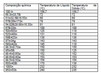
[0080] Uma lista exemplificadora de polímeros termoplásticos que podem ser utilizados com modalidades da invenção é fornecida na Tabela 3.
[0081] A Figura 15 é um fluxograma que ilustra um método de coletar e transferir um microdispositivo de um substrato de carreador para um substrato de recepção de acordo com uma modalidade da invenção. Na operação 1510, uma cabeça de transferência é posicionada sobre um microdispositivo conectado a um substrato de carreador com uma camada de ligação. A cabeça de transferência pode ser qualquer cabeça de transferência descrita na presente invenção. O microdispositivo pode ser qualquer uma dentre as estruturas de dispositivo micro-LED ilustradas nas Figuras 27 a 29 e aquelas descritas no Pedido Provisório relacionado no. US 61/561.706 e o Pedido Provisório no. US 61/594.919. O microdispositivo é, então, colocado em contato com a cabeça de transferência na operação 1520. Em uma modalidade, o microdispositivo é colocado em contato com a camada dielétrica 120 da cabeça de transferência. Em uma modalidade alternativa, a cabeça de transferência é posicionada sobre o microdispositivo com um vão de ar adequado que separa os mesmos que não afeta de forma significativa a pressão de pega, por exemplo, 1 nm (0,001 μm) ou 10 nm (0,01 μm). Na operação 1525, uma operação é realizada para criar uma mudança de fase na camada de ligação 210 do estado sólido para líquido. Por exemplo, a operação pode incluir aquecer uma camada de ligação In para ou acima da temperatura de fusão de 156,7 oC. Em uma outra modalidade, a operação 1525 pode ser realizada antes da operação 1520. Na operação 1530, uma tensão é aplicada ao eletrodo para criar uma pressão de pega no microdispositivo e o microdispositivo e uma porção da camada de ligação substancial 210 são coletadas com a cabeça de transferência na operação 1540. Por exemplo, aproximadamente metade da camada de ligação 210 pode ser coletada com o microdispositivo. Em uma modalidade alternativa, nenhuma da camada de ligação 210 é coletada com a cabeça de transferência. Na operação 1545, o microdispositivo e a porção da camada de ligação 210 são colocados em contato com um substrato de recepção. O microdispositivo e uma porção da camada de ligação 210 são, então, liberados no substrato de recepção na operação 1550. Uma variedade de operações pode ser realizada para controlar a fase da porção da camada de ligação ao coletar, transferir, colocar em contato a substrato de recepção e liberar o microdispositivo e porção da camada de ligação 210 no substrato de recepção. Por exemplo, a porção da camada de ligação que é coletada com o microdispositivo pode ser mantida no estado líquido durante a operação de colocação em contato 1545 e durante a operação de liberação 1550. Em uma outra modalidade, a porção da camada de ligação pode ser permitida a resfriar para uma fase sólida após ser coletada. Por exemplo, a porção da camada de ligação pode estar em uma fase sólida durante a operação de colocação em contato 1545 e novamente fundida para o estado líquido antes ou durante a operação de liberação 1550. Uma variedade de ciclos de temperatura e fase de material pode ser realizada de acordo com modalidades da invenção.[0081] Figure 15 is a flow chart illustrating a method of collecting and transferring a microdevice from a carrier substrate to a receiving substrate according to an embodiment of the invention. In
[0082] A Figura 16 é um fluxograma que ilustra um método de coletar e transferir um arranjo de microdispositivos de um substrato de carreador para pelo menos um substrato de recepção de acordo com uma modalidade da invenção. Na operação 1610, um arranjo de cabeças de transferência é posicionado sobre um arranjo de microdispositivos, sendo que cada cabeça de transferência tem uma estrutura de mesa, um eletrodo sobre a estrutura de mesa e uma camada dielétrica que cobre o eletrodo. Na operação 1620, o arranjo de microdispositivos é colocado em contato com o arranjo de cabeças de transferência. Em uma modalidade alternativa, o arranjo de cabeças de transferência é posicionado sobre o arranjo de microdispositivos com um vão de ar adequado que separa os mesmos que não afeta de forma significativa a pressão de pega, por exemplo, 1 nm (0,001 μm) ou 10 nm (0,01 μm). A Figura 17 é uma ilustração de vista lateral de um arranjo de cabeças de transferência de microdispositivo 100 em contato com um arranjo de dispositivos micro- LED 200 de acordo com uma modalidade da invenção. Conforme ilustrado na Figura 17, o passo (P) do arranjo de cabeças de transferência 100 corresponde ao passo dos dispositivos micro-LED 200 com o passo (P) do arranjo de cabeças de transferência sendo a soma do espaçamento (S) entre cabeças de transferência com a largura (W) de uma cabeça de transferência.[0082] Figure 16 is a flow chart illustrating a method of collecting and transferring an array of microdevices from a carrier substrate to at least one receiving substrate according to one embodiment of the invention. In
[0083] Em uma modalidade, o arranjo de dispositivos micro-LED 200 tem um passo de 10 μm, com cada dispositivo micro-LED tendo um espaçamento de 2 μm e uma largura máxima de 8 μm. Em uma modalidade exemplificadora, assume-se que em um micro-diodo p-n 250 com paredes laterais retas, a superfície de topo de cada dispositivo micro-LED 200 tem uma largura de aproximadamente 8 μm. Em tal modalidade exemplificadora, a largura da superfície de topo 121 de uma cabeça de transferência correspondente 100 é aproximadamente 8 μm ou menor de forma a evitar fazer contato involuntário com um dispositivo micro-LED adjacente. Em uma outra modalidade, o arranjo de dispositivos micro-LED 200 pode ter um passo de 5 μm, sendo que cada dispositivo micro-LED tem um espaçamento de 2 μm e uma largura máxima de 3 μm. Em uma modalidade exemplificadora, a superfície de topo de cada dispositivo micro-LED 200 tem uma largura de aproximadamente 3 μm. Em tal modalidade exemplificadora, a largura da superfície de topo 121 de uma cabeça de transferência correspondente 100 é aproximadamente 3 μm ou menor de forma a evitar fazer contato involuntário com um dispositivo micro-LED adjacente 200. Entretanto, modalidades da invenção não são limitadas a essas dimensões específicas e podem ser de qualquer dimensão adequada.[0083] In one embodiment, the array of
[0084] A Figura 18 é uma ilustração de vista lateral de um arranjo de cabeças de transferência de microdispositivo em contato com um arranjo de dispositivos micro-LED 200 de acordo com uma modalidade da invenção. Na modalidade ilustrada na Figura 18, o passo (P) das cabeças de transferência é um inteiro múltiplo do passo do arranjo de microdispositivos. Na modalidade em particular ilustrada, o passo (P) das cabeças de transferência é 3 vezes o passo do arranjo de dispositivos micro-LED. Em tal modalidade, ter um passo de cabeça de transferência maior pode proteger contra arqueamento entre cabeças de transferência.[0084] Figure 18 is a side view illustration of an array of microdevice transfer heads in contact with an array of
[0085] Com referência novamente à Figura 16, na operação 1630, uma tensão é aplicada seletivamente a uma porção do arranjo de cabeças de transferência 100. Portanto, cada cabeça de transferência 100 pode ser operada de forma independente. Na operação 1640, uma porção correspondente do arranjo de microdispositivos é coletada com a porção do arranjo de cabeças de transferência à qual a tensão foi aplicada seletivamente. Em uma modalidade, aplicar seletivamente uma tensão a uma porção do arranjo de cabeças de transferência significa aplicar uma tensão a cada cabeça de transferência no arranjo de cabeças de transferência. A Figura 19 é uma ilustração de vista lateral de cada cabeça de transferência em um arranjo de cabeças de transferência de microdispositivo que coleta um arranjo de dispositivos micro-LED 200 de acordo com uma modalidade da invenção. Em uma outra modalidade, aplicar seletivamente uma tensão a uma porção do arranjo de cabeças de transferência significa aplicar uma tensão a menos que todas as cabeças de transferência (por exemplo, um subconjunto de cabeças de transferência) no arranjo de cabeças de transferência. A Figura 20 é uma ilustração de vista lateral de um subconjunto do arranjo de cabeças de transferência de microdispositivo que coletam uma porção de um arranjo de dispositivos micro-LED 200 de acordo com uma modalidade da invenção. Em uma modalidade em particular ilustrada nas Figuras 19 a 20, a operação de coleta inclui coletar o micro-diodo p-n 250, a camada de metalização 220 e uma porção da camada de barreira dielétrica conformal 260 para o dispositivo micro-LED 200. Em uma modalidade em particular ilustrada nas Figuras 19 a 20, a operação de coleta inclui coletar uma porção substancial da camada de ligação 210. Consequentemente, qualquer uma das modalidades descritas em relação às Figuras 16 a 22 também pode ser obtida pelo controle da temperatura da porção da camada de ligação 210 conforme descrito em relação à Figura 15. Por exemplo, modalidades descritas em relação às Figuras 16 a 22 podem incluir realizar uma operação para criar uma mudança de fase de estado sólido para líquido em uma pluralidade de localizações da camada de ligação que conectam o arranjo de microdispositivos ao substrato de carreador 201 antes de coletar o arranjo de microdispositivos. Em uma modalidade, a pluralidade de localizações da camada de ligação pode ser regiões da mesma camada de ligação. Em uma modalidade, a pluralidade de localizações da camada de ligação pode ser localizações separadas lateralmente da camada de ligação.[0085] With reference again to Figure 16, in
[0086] Em operação 1650, a porção do arranjo de microdispositivos é, então, liberada em pelo menos um substrato de recepção. Assim, o arranjo de micro LEDs pode ser totalmente liberado em um único substrato de recepção ou liberado seletivamente em múltiplos substratos. Por exemplo, o substrato de recepção pode ser, mas não é limitado a, um substrato de exibição, um substrato de iluminação, um substrato com dispositivos funcionais como transistores ou ICs ou um substrato com linhas de redistribuição de metais. A liberação pode ser obtida ao efetuar a tensão aplicada com qualquer uma das maneiras descritas em relação às Figuras 12 a 14.[0086] In
[0087] A Figura 21 é uma ilustração de vista lateral de um arranjo de cabeças de transferência de microdispositivo que retém um arranjo correspondente de dispositivos micro-LED 200 sobre um substrato de recepção 301 que inclui a pluralidade de contatos acionadores 310. O arranjo de dispositivos micro-LED 200 pode, então, ser colocado em contato com o substrato de recepção e, então, liberado seletivamente. A Figura 22 é uma ilustração de vista lateral de um único dispositivo micro-LED 200 liberado seletivamente no substrato de recepção 301 sobre um contato acionador 310 de acordo com uma modalidade da invenção. Em uma outra modalidade, mais de um dispositivo micro- LED 200 é liberado ou o arranjo inteiro de dispositivos micro-LED 200 é liberado.[0087] Figure 21 is a side view illustration of an array of microdevice transfer heads that retain a corresponding array of
[0088] Ao utilizar os vários aspectos dessa invenção, se tornará aparente ao versado na técnica que combinações ou variações das modalidades acima são possíveis para formar uma cabeça de transferência de microdispositivo e arranjo de cabeça e para transferir um microdispositivo e arranjo de microdispositivo. Embora a presente invenção tenha sido descrita em linguagem específica para recursos estruturais e/ou atos metodológicos, deve ser compreendido que a invenção definida nas concretizações não é necessariamente limitada aos recursos ou atos específicos descritos. Os recursos e atos específicos revelados devem, ao invés disso, ser compreendidos como implantações particularmente elegantes da invenção reivindicada úteis para ilustrar a presente invenção.[0088] By using the various aspects of this invention, it will become apparent to the person skilled in the art that combinations or variations of the above modalities are possible to form a microdevice transfer head and head arrangement and to transfer a microdevice and microdevice arrangement. Although the present invention has been described in specific language for structural features and / or methodological acts, it should be understood that the invention defined in the embodiments is not necessarily limited to the specific features or acts described. The specific features and acts disclosed should, instead, be understood as particularly elegant implementations of the claimed invention useful to illustrate the present invention.
Claims (20)
Applications Claiming Priority (12)
| Application Number | Priority Date | Filing Date | Title |
|---|---|---|---|
| US201161561706P | 2011-11-18 | 2011-11-18 | |
| US201261594919P | 2012-02-03 | 2012-02-03 | |
| US61/594,919 | 2012-02-03 | ||
| US201261597109P | 2012-02-09 | 2012-02-09 | |
| US61/597,109 | 2012-02-09 | ||
| US13/372,310 US8333860B1 (en) | 2011-11-18 | 2012-02-13 | Method of transferring a micro device |
| US13/372,310 | 2012-02-13 | ||
| US13/372,277 | 2012-02-13 | ||
| US13/372,277 US8646505B2 (en) | 2011-11-18 | 2012-02-13 | Micro device transfer head |
| US13/372,292 | 2012-02-13 | ||
| US13/372,292 US9620478B2 (en) | 2011-11-18 | 2012-02-13 | Method of fabricating a micro device transfer head |
| PCT/US2012/063990 WO2013074355A1 (en) | 2011-11-18 | 2012-11-07 | Micro device transfer head |
Publications (2)
| Publication Number | Publication Date |
|---|---|
| BR112014011800A2 BR112014011800A2 (en) | 2017-05-09 |
| BR112014011800B1 true BR112014011800B1 (en) | 2020-12-22 |
Family
ID=47325228
Family Applications (2)
| Application Number | Title | Priority Date | Filing Date |
|---|---|---|---|
| BR112014011826-4A BR112014011826B1 (en) | 2011-11-18 | 2012-11-07 | METHOD TO DOWNLOAD A MICRODEVICE AND METHOD TO DOWNLOAD A MICRODEVICE ARRANGEMENT |
| BR112014011800-0A BR112014011800B1 (en) | 2011-11-18 | 2012-11-07 | bipolar electrostatic transfer head |
Family Applications Before (1)
| Application Number | Title | Priority Date | Filing Date |
|---|---|---|---|
| BR112014011826-4A BR112014011826B1 (en) | 2011-11-18 | 2012-11-07 | METHOD TO DOWNLOAD A MICRODEVICE AND METHOD TO DOWNLOAD A MICRODEVICE ARRANGEMENT |
Country Status (11)
| Country | Link |
|---|---|
| US (3) | US8333860B1 (en) |
| EP (2) | EP2780934B1 (en) |
| JP (3) | JP2015507839A (en) |
| KR (3) | KR101622061B1 (en) |
| CN (3) | CN104067379B (en) |
| AU (2) | AU2012339923B2 (en) |
| BR (2) | BR112014011826B1 (en) |
| IN (2) | IN2014CN03734A (en) |
| MX (2) | MX336548B (en) |
| TW (3) | TWI579958B (en) |
| WO (3) | WO2013074355A1 (en) |
Families Citing this family (221)
| Publication number | Priority date | Publication date | Assignee | Title |
|---|---|---|---|---|
| US8877648B2 (en) | 2009-03-26 | 2014-11-04 | Semprius, Inc. | Methods of forming printable integrated circuit devices by selective etching to suspend the devices from a handling substrate and devices formed thereby |
| US8349116B1 (en) | 2011-11-18 | 2013-01-08 | LuxVue Technology Corporation | Micro device transfer head heater assembly and method of transferring a micro device |
| US8794501B2 (en) | 2011-11-18 | 2014-08-05 | LuxVue Technology Corporation | Method of transferring a light emitting diode |
| US8573469B2 (en) | 2011-11-18 | 2013-11-05 | LuxVue Technology Corporation | Method of forming a micro LED structure and array of micro LED structures with an electrically insulating layer |
| US8518204B2 (en) | 2011-11-18 | 2013-08-27 | LuxVue Technology Corporation | Method of fabricating and transferring a micro device and an array of micro devices utilizing an intermediate electrically conductive bonding layer |
| US8333860B1 (en) | 2011-11-18 | 2012-12-18 | LuxVue Technology Corporation | Method of transferring a micro device |
| US9773750B2 (en) | 2012-02-09 | 2017-09-26 | Apple Inc. | Method of transferring and bonding an array of micro devices |
| US9548332B2 (en) | 2012-04-27 | 2017-01-17 | Apple Inc. | Method of forming a micro LED device with self-aligned metallization stack |
| US9105492B2 (en) * | 2012-05-08 | 2015-08-11 | LuxVue Technology Corporation | Compliant micro device transfer head |
| US9034754B2 (en) | 2012-05-25 | 2015-05-19 | LuxVue Technology Corporation | Method of forming a micro device transfer head with silicon electrode |
| US8569115B1 (en) | 2012-07-06 | 2013-10-29 | LuxVue Technology Corporation | Method of forming a compliant bipolar micro device transfer head with silicon electrodes |
| US9557215B2 (en) | 2012-08-17 | 2017-01-31 | Massachusetts Institute Of Technology | Phonon-recyling light-emitting diodes |
| US8791530B2 (en) | 2012-09-06 | 2014-07-29 | LuxVue Technology Corporation | Compliant micro device transfer head with integrated electrode leads |
| US9162880B2 (en) | 2012-09-07 | 2015-10-20 | LuxVue Technology Corporation | Mass transfer tool |
| US8941215B2 (en) | 2012-09-24 | 2015-01-27 | LuxVue Technology Corporation | Micro device stabilization post |
| US8835940B2 (en) | 2012-09-24 | 2014-09-16 | LuxVue Technology Corporation | Micro device stabilization post |
| US9558721B2 (en) | 2012-10-15 | 2017-01-31 | Apple Inc. | Content-based adaptive refresh schemes for low-power displays |
| US9255001B2 (en) | 2012-12-10 | 2016-02-09 | LuxVue Technology Corporation | Micro device transfer head array with metal electrodes |
| US9236815B2 (en) | 2012-12-10 | 2016-01-12 | LuxVue Technology Corporation | Compliant micro device transfer head array with metal electrodes |
| US9166114B2 (en) | 2012-12-11 | 2015-10-20 | LuxVue Technology Corporation | Stabilization structure including sacrificial release layer and staging cavity |
| US9105714B2 (en) | 2012-12-11 | 2015-08-11 | LuxVue Technology Corporation | Stabilization structure including sacrificial release layer and staging bollards |
| US9391042B2 (en) * | 2012-12-14 | 2016-07-12 | Apple Inc. | Micro device transfer system with pivot mount |
| US9314930B2 (en) | 2012-12-14 | 2016-04-19 | LuxVue Technology Corporation | Micro pick up array with integrated pivot mount |
| CN105074899B (en) * | 2013-02-25 | 2017-06-09 | 苹果公司 | Mass transfer tool manipulator assembly and micropickup array mount with integrated displacement sensors |
| US9308649B2 (en) | 2013-02-25 | 2016-04-12 | LuxVue Techonology Corporation | Mass transfer tool manipulator assembly |
| US9095980B2 (en) * | 2013-02-25 | 2015-08-04 | LuxVue Technology Corporation | Micro pick up array mount with integrated displacement sensor |
| US8791474B1 (en) | 2013-03-15 | 2014-07-29 | LuxVue Technology Corporation | Light emitting diode display with redundancy scheme |
| US9252375B2 (en) | 2013-03-15 | 2016-02-02 | LuxVue Technology Corporation | Method of fabricating a light emitting diode display with integrated defect detection test |
| US9484504B2 (en) | 2013-05-14 | 2016-11-01 | Apple Inc. | Micro LED with wavelength conversion layer |
| US9217541B2 (en) | 2013-05-14 | 2015-12-22 | LuxVue Technology Corporation | Stabilization structure including shear release posts |
| US9136161B2 (en) | 2013-06-04 | 2015-09-15 | LuxVue Technology Corporation | Micro pick up array with compliant contact |
| JP6854643B2 (en) | 2013-06-12 | 2021-04-07 | ロヒンニ リミテッド ライアビリティ カンパニー | Keyboard back lighting with attached light source |
| US8987765B2 (en) | 2013-06-17 | 2015-03-24 | LuxVue Technology Corporation | Reflective bank structure and method for integrating a light emitting device |
| US9111464B2 (en) | 2013-06-18 | 2015-08-18 | LuxVue Technology Corporation | LED display with wavelength conversion layer |
| US8928021B1 (en) | 2013-06-18 | 2015-01-06 | LuxVue Technology Corporation | LED light pipe |
| US9035279B2 (en) | 2013-07-08 | 2015-05-19 | LuxVue Technology Corporation | Micro device with stabilization post |
| US9296111B2 (en) | 2013-07-22 | 2016-03-29 | LuxVue Technology Corporation | Micro pick up array alignment encoder |
| US9087764B2 (en) | 2013-07-26 | 2015-07-21 | LuxVue Technology Corporation | Adhesive wafer bonding with controlled thickness variation |
| US9722144B2 (en) | 2013-08-16 | 2017-08-01 | Massachusetts Institute Of Technology | Phonon-recycling light-emitting diodes |
| US9153548B2 (en) | 2013-09-16 | 2015-10-06 | Lux Vue Technology Corporation | Adhesive wafer bonding with sacrificial spacers for controlled thickness variation |
| US9367094B2 (en) | 2013-12-17 | 2016-06-14 | Apple Inc. | Display module and system applications |
| US9768345B2 (en) | 2013-12-20 | 2017-09-19 | Apple Inc. | LED with current injection confinement trench |
| US9450147B2 (en) | 2013-12-27 | 2016-09-20 | Apple Inc. | LED with internally confined current injection area |
| US9583466B2 (en) | 2013-12-27 | 2017-02-28 | Apple Inc. | Etch removal of current distribution layer for LED current confinement |
| US9542638B2 (en) | 2014-02-18 | 2017-01-10 | Apple Inc. | RFID tag and micro chip integration design |
| US9583533B2 (en) | 2014-03-13 | 2017-02-28 | Apple Inc. | LED device with embedded nanowire LEDs |
| US9522468B2 (en) | 2014-05-08 | 2016-12-20 | Apple Inc. | Mass transfer tool manipulator assembly with remote center of compliance |
| US9318475B2 (en) | 2014-05-15 | 2016-04-19 | LuxVue Technology Corporation | Flexible display and method of formation with sacrificial release layer |
| US9741286B2 (en) | 2014-06-03 | 2017-08-22 | Apple Inc. | Interactive display panel with emitting and sensing diodes |
| US9624100B2 (en) | 2014-06-12 | 2017-04-18 | Apple Inc. | Micro pick up array pivot mount with integrated strain sensing elements |
| US9425151B2 (en) | 2014-06-17 | 2016-08-23 | Apple Inc. | Compliant electrostatic transfer head with spring support layer |
| US9570002B2 (en) | 2014-06-17 | 2017-02-14 | Apple Inc. | Interactive display panel with IR diodes |
| CN113035850B (en) | 2014-06-18 | 2022-12-06 | 艾克斯展示公司技术有限公司 | Micro-assembly LED display |
| KR102181010B1 (en) | 2014-07-20 | 2020-11-20 | 엑스-셀레프린트 리미티드 | Apparatus and methods for micro-transfer printing |
| GB201413578D0 (en) | 2014-07-31 | 2014-09-17 | Infiniled Ltd | A colour iled display on silicon |
| US9828244B2 (en) | 2014-09-30 | 2017-11-28 | Apple Inc. | Compliant electrostatic transfer head with defined cavity |
| US9705432B2 (en) | 2014-09-30 | 2017-07-11 | Apple Inc. | Micro pick up array pivot mount design for strain amplification |
| US10381335B2 (en) | 2014-10-31 | 2019-08-13 | ehux, Inc. | Hybrid display using inorganic micro light emitting diodes (uLEDs) and organic LEDs (OLEDs) |
| US9825202B2 (en) | 2014-10-31 | 2017-11-21 | eLux, Inc. | Display with surface mount emissive elements |
| US10520769B2 (en) | 2014-10-31 | 2019-12-31 | eLux, Inc. | Emissive display with printed light modification structures |
| US10319878B2 (en) | 2014-10-31 | 2019-06-11 | eLux, Inc. | Stratified quantum dot phosphor structure |
| US10236279B2 (en) | 2014-10-31 | 2019-03-19 | eLux, Inc. | Emissive display with light management system |
| US10543486B2 (en) | 2014-10-31 | 2020-01-28 | eLux Inc. | Microperturbation assembly system and method |
| US10535640B2 (en) | 2014-10-31 | 2020-01-14 | eLux Inc. | System and method for the fluidic assembly of micro-LEDs utilizing negative pressure |
| US10242977B2 (en) | 2014-10-31 | 2019-03-26 | eLux, Inc. | Fluid-suspended microcomponent harvest, distribution, and reclamation |
| US10418527B2 (en) | 2014-10-31 | 2019-09-17 | eLux, Inc. | System and method for the fluidic assembly of emissive displays |
| US10381332B2 (en) | 2014-10-31 | 2019-08-13 | eLux Inc. | Fabrication method for emissive display with light management system |
| US10446728B2 (en) | 2014-10-31 | 2019-10-15 | eLux, Inc. | Pick-and remove system and method for emissive display repair |
| CN104465474B (en) * | 2014-11-14 | 2017-09-15 | 昆山工研院新型平板显示技术中心有限公司 | Display device transfers positioner and its method |
| US10984821B1 (en) | 2014-11-19 | 2021-04-20 | Seagate Technology Llc | Transfer-printed near-field transducer and heat sink |
| US9607638B1 (en) | 2014-11-19 | 2017-03-28 | Seagate Technology Llc | Recording head with an on-wafer integrated laser |
| US9576595B1 (en) | 2014-11-19 | 2017-02-21 | Seagate Technology Llc | Transfer printing an epitaxial layer to a read/write head to form an integral laser |
| US10069029B1 (en) | 2014-11-19 | 2018-09-04 | Seagate Technology Llc | Transfer-printed photonics |
| US9607907B2 (en) | 2014-12-01 | 2017-03-28 | Industrial Technology Research Institute | Electric-programmable magnetic module and picking-up and placement process for electronic devices |
| US9773711B2 (en) | 2014-12-01 | 2017-09-26 | Industrial Technology Research Institute | Picking-up and placing process for electronic devices and electronic module |
| US9478583B2 (en) | 2014-12-08 | 2016-10-25 | Apple Inc. | Wearable display having an array of LEDs on a conformable silicon substrate |
| CN107431107B (en) | 2015-04-01 | 2020-07-24 | 歌尔股份有限公司 | Micro light emitting diode transfer method, manufacturing method, device and electronic equipment |
| WO2016160322A1 (en) | 2015-04-01 | 2016-10-06 | Sxaymiq Technologies Llc | Electrostatic cleaning device |
| KR101614370B1 (en) * | 2015-04-07 | 2016-04-21 | 엘지전자 주식회사 | Semiconductor light emitting device, transfer head of the semiconductor light emitting device, and method for transferring the semiconductor light emitting device |
| JP6375063B2 (en) * | 2015-05-21 | 2018-08-15 | ゴルテック.インク | Micro light-emitting diode transport method, manufacturing method, apparatus, and electronic apparatus |
| EP3221903B1 (en) | 2015-07-14 | 2019-06-19 | Goertek Inc | Transferring method of micro-led, and manufacturing method of micro-led device |
| JP6398008B2 (en) * | 2015-07-14 | 2018-09-26 | ゴルテック.インク | Flip die assembly method, manufacturing method, apparatus, and electronic apparatus |
| EP3323145A1 (en) | 2015-07-14 | 2018-05-23 | Goertek Inc. | Transferring method, manufacturing method, device and electronic apparatus of micro-led |
| GB201512600D0 (en) * | 2015-07-17 | 2015-08-26 | Koniku Ltd | Cell culture, transport and investigation |
| US9704821B2 (en) | 2015-08-11 | 2017-07-11 | X-Celeprint Limited | Stamp with structured posts |
| TWI566918B (en) * | 2015-07-29 | 2017-01-21 | 財團法人工業技術研究院 | Three-dimensional printing system |
| US10373856B2 (en) | 2015-08-03 | 2019-08-06 | Mikro Mesa Technology Co., Ltd. | Transfer head array |
| US9969078B2 (en) * | 2015-08-03 | 2018-05-15 | Mikro Mesa Technology Co., Ltd. | Transfer head array and transferring method |
| KR101718717B1 (en) * | 2015-08-11 | 2017-04-04 | (주)다원넥스뷰 | Probe Bonding Device and Probe Bonding Method Using the Same |
| US10179731B2 (en) | 2015-08-17 | 2019-01-15 | Mikro Mesa Technology Co., Ltd. | Transfer head array |
| US10020420B2 (en) | 2015-08-18 | 2018-07-10 | Goertek Inc. | Repairing method, manufacturing method, device and electronic apparatus of micro-LED |
| US10177016B2 (en) | 2015-08-18 | 2019-01-08 | Goertek Inc. | Pre-screening method, manufacturing method, device and electronic apparatus of micro-LED |
| KR102402189B1 (en) * | 2015-08-26 | 2022-05-25 | 엘지전자 주식회사 | Transfer unit for micro device |
| US10950583B2 (en) | 2015-08-26 | 2021-03-16 | Lg Electronics Inc. | Transfer head and transfer system for semiconductor light-emitting device and method for transferring semiconductor light-emitting device |
| US10297719B2 (en) | 2015-08-27 | 2019-05-21 | Mikro Mesa Technology Co., Ltd. | Micro-light emitting diode (micro-LED) device |
| KR102402999B1 (en) * | 2015-08-31 | 2022-05-30 | 삼성디스플레이 주식회사 | Display apparatus and method of manufacturing the same |
| EP3257072B1 (en) * | 2015-09-09 | 2019-03-06 | Goertek Inc | Repairing method and manufacturing method of micro-led device |
| US10230048B2 (en) | 2015-09-29 | 2019-03-12 | X-Celeprint Limited | OLEDs for micro transfer printing |
| US9865779B2 (en) | 2015-09-30 | 2018-01-09 | Nichia Corporation | Methods of manufacturing the package and light-emitting device |
| JP6237826B2 (en) * | 2015-09-30 | 2017-11-29 | 日亜化学工業株式会社 | Package, light emitting device, and manufacturing method thereof |
| EP3262694B1 (en) | 2015-10-20 | 2019-08-21 | Goertek. Inc | Method for transferring micro-leds and method for manufacturing micro-led device |
| CN105723528A (en) | 2015-11-04 | 2016-06-29 | 歌尔声学股份有限公司 | Transfer method, manufacturing method, device and electronic equipment of micro light emitting diode |
| KR102427644B1 (en) | 2015-11-16 | 2022-08-02 | 삼성전자주식회사 | Light source, method of manufacturing the same, and display apparatus having the same |
| KR20170059068A (en) | 2015-11-19 | 2017-05-30 | 삼성전자주식회사 | Lighting source module, display panel and display apparatus |
| CN113421839B (en) | 2015-12-23 | 2022-03-18 | 歌尔股份有限公司 | Micro light emitting diode transfer method and manufacturing method |
| WO2017124109A1 (en) | 2016-01-15 | 2017-07-20 | Rohinni, LLC | Apparatus and method of backlighting through a cover on the apparatus |
| TWI681508B (en) * | 2016-02-25 | 2020-01-01 | 愛爾蘭商艾克斯瑟樂普林特有限公司 | Efficiently micro-transfer printing micro-scale devices onto large-format substrates |
| US10150325B2 (en) | 2016-02-29 | 2018-12-11 | X-Celeprint Limited | Hybrid banknote with electronic indicia |
| KR102562627B1 (en) | 2016-03-21 | 2023-08-03 | 삼성디스플레이 주식회사 | Display device |
| KR101754528B1 (en) * | 2016-03-23 | 2017-07-06 | 한국광기술원 | Transfer assembly with dry adhesion structure and method for transferring led structure assembly using the same and led structure assembly |
| US10622700B2 (en) | 2016-05-18 | 2020-04-14 | X-Celeprint Limited | Antenna with micro-transfer-printed circuit element |
| US11262376B2 (en) * | 2016-06-02 | 2022-03-01 | Weifang Goertek Microelectronics Co., Ltd. | MEMS device and electronic apparatus |
| US9997399B2 (en) | 2016-08-16 | 2018-06-12 | Mikro Mesa Technology Co., Ltd. | Method for transferring semiconductor structure |
| WO2018082102A1 (en) * | 2016-11-07 | 2018-05-11 | Goertek.Inc | Micro-led transfer method and manufacturing method |
| US10783917B1 (en) | 2016-11-29 | 2020-09-22 | Seagate Technology Llc | Recording head with transfer-printed laser diode unit formed of non-self-supporting layers |
| JP2020510417A (en) | 2017-02-17 | 2020-04-09 | コニク インコーポレイテッド | System for detection |
| US20180240931A1 (en) * | 2017-02-23 | 2018-08-23 | Novatek Microelectronics Corp. | Micro-device panel and manufacturing process thereof |
| TWI624044B (en) | 2017-03-15 | 2018-05-11 | 啟端光電股份有限公司 | Micro component transfer system |
| TWI605536B (en) | 2017-04-12 | 2017-11-11 | 財團法人工業技術研究院 | Magnetic transfer module and method for transferring electronic components |
| TWI623053B (en) | 2017-04-12 | 2018-05-01 | 宏碁股份有限公司 | Method for transferring minute components and device for transferring minute components |
| US10468397B2 (en) | 2017-05-05 | 2019-11-05 | X-Celeprint Limited | Matrix addressed tiles and arrays |
| US10604843B2 (en) | 2017-05-10 | 2020-03-31 | Xerox Corporation | High registration particles-transferring system |
| US10734269B1 (en) * | 2017-06-07 | 2020-08-04 | Apple Inc. | Micro device metal joint process |
| KR101937036B1 (en) | 2017-06-28 | 2019-04-09 | 한국광기술원 | Method for transferring led structure assembly and led structure assembly |
| US11227787B2 (en) | 2017-07-14 | 2022-01-18 | Industrial Technology Research Institute | Transfer support and transfer module |
| US10431483B2 (en) | 2017-07-14 | 2019-10-01 | Industrial Technology Research Institute | Transfer support and transfer module |
| CN109256354B (en) * | 2017-07-14 | 2021-01-12 | 财团法人工业技术研究院 | Transfer support and transfer module |
| KR101959057B1 (en) | 2017-07-21 | 2019-03-18 | 한국광기술원 | Transfering method and apparatus of micro LED chip |
| TWI633618B (en) * | 2017-08-02 | 2018-08-21 | 李美燕 | Integrated microgripper, method of manufacturing the same and microgripper array and transfer system using the same |
| KR102572669B1 (en) * | 2017-08-14 | 2023-08-31 | 삼성전자주식회사 | Transfering apparatus for electrical element |
| KR102123348B1 (en) | 2017-09-28 | 2020-06-16 | 시바우라 메카트로닉스 가부시끼가이샤 | Device and method for mounting element and method for manufacturing a substrate on which an element is mounted |
| TWI647810B (en) * | 2017-10-13 | 2019-01-11 | 行家光電股份有限公司 | Method and system for mass arrangement of micro devices |
| US10748792B2 (en) | 2017-10-13 | 2020-08-18 | Maven Optronics Co., Ltd. | Method and system for mass arrangement of micro-component devices |
| US10836200B2 (en) | 2017-11-13 | 2020-11-17 | X Display Company Technology Limited | Rigid micro-modules with ILED and light conductor |
| TWI654465B (en) | 2017-11-13 | 2019-03-21 | 友達光電股份有限公司 | Transfer head and transfer device |
| TWI626772B (en) * | 2017-11-13 | 2018-06-11 | Au Optronics Corporation | Transposition device |
| CN107978548B (en) * | 2017-11-20 | 2019-07-05 | 厦门市三安光电科技有限公司 | The flood tide transfer method of microcomponent |
| TWI637481B (en) | 2017-11-29 | 2018-10-01 | 財團法人工業技術研究院 | Semiconductor structure, light emitting device and method of manufacturing same |
| TWI679748B (en) * | 2017-12-19 | 2019-12-11 | 英屬開曼群島商錼創科技股份有限公司 | Structure with micro device |
| US10236195B1 (en) | 2017-12-20 | 2019-03-19 | Mikro Mesa Technology Co., Ltd. | Method for transferring device |
| WO2019132050A1 (en) * | 2017-12-26 | 2019-07-04 | 박일우 | Led display device and method for manufacturing same |
| CN110034058A (en) * | 2018-01-11 | 2019-07-19 | 美科米尚技术有限公司 | Transposition head array |
| US10325889B1 (en) | 2018-01-12 | 2019-06-18 | Mikro Mesa Technology Co., Ltd. | Display device including LED devices with selective activation function |
| US11423928B1 (en) | 2018-01-19 | 2022-08-23 | Seagate Technology Llc | Processing for forming single-grain near-field transducer |
| KR20190091022A (en) | 2018-01-26 | 2019-08-05 | 주식회사 싸인랩 | Method and apparatus for displaying Character Floating Hologram by Depth Video |
| US10937674B2 (en) * | 2018-02-13 | 2021-03-02 | Mikro Mesa Technology Co., Ltd. | Method for transferring micro device |
| US11069376B1 (en) | 2018-02-21 | 2021-07-20 | Seagate Technology Llc | Waveguide with optical isolator for heat-assisted magnetic recording |
| US10593582B2 (en) * | 2018-02-26 | 2020-03-17 | Mikro Mesa Technology Co., Ltd. | Transfer head and method for transferring micro devices |
| US10593581B2 (en) * | 2018-02-26 | 2020-03-17 | Mikro Mesa Technology Co., Ltd. | Transfer head and method for transferring micro devices |
| US11189605B2 (en) | 2018-02-28 | 2021-11-30 | X Display Company Technology Limited | Displays with transparent bezels |
| KR102076904B1 (en) | 2018-03-16 | 2020-02-12 | 한국광기술원 | Led transfer tool |
| KR102486822B1 (en) | 2018-03-29 | 2023-01-10 | 삼성전자주식회사 | Chip transfer device and chip transfering method using the same |
| KR20190114330A (en) * | 2018-03-29 | 2019-10-10 | (주)포인트엔지니어링 | Transfer head for micro led |
| US10910355B2 (en) | 2018-04-30 | 2021-02-02 | X Display Company Technology Limited | Bezel-free displays |
| KR20190133988A (en) | 2018-05-24 | 2019-12-04 | (주)피엔티 | Micro-LED On-Board Placing method and Placing device |
| US10832934B2 (en) | 2018-06-14 | 2020-11-10 | X Display Company Technology Limited | Multi-layer tethers for micro-transfer printing |
| KR20200005237A (en) * | 2018-07-06 | 2020-01-15 | (주)포인트엔지니어링 | Micro led transfer head and micro led transfer system using the same |
| KR102558296B1 (en) | 2018-07-10 | 2023-07-24 | 삼성전자주식회사 | Electronic apparatus, method for manufacturing led module and computer-readable recording medium |
| KR102782924B1 (en) | 2018-07-23 | 2025-03-19 | 삼성전자주식회사 | Electronic apparatus including led transmission device and controlling method thereof |
| US12236825B2 (en) | 2018-08-13 | 2025-02-25 | X Display Company Technology Limited | Redundant pixel layouts |
| JP7132040B2 (en) * | 2018-08-30 | 2022-09-06 | 芝浦メカトロニクス株式会社 | Device mounting apparatus and device mounting substrate manufacturing method |
| US11387029B2 (en) | 2018-09-12 | 2022-07-12 | LuxNour Technologies Inc. | Apparatus for transferring plurality of micro devices and methods of fabrication |
| TWI676980B (en) * | 2018-09-27 | 2019-11-11 | 友達光電股份有限公司 | monitor |
| KR102590229B1 (en) | 2018-10-15 | 2023-10-17 | 삼성전자주식회사 | Light emitting diode, manufacturing method of light emitting diode |
| US10573544B1 (en) | 2018-10-17 | 2020-02-25 | X-Celeprint Limited | Micro-transfer printing with selective component removal |
| US10796938B2 (en) | 2018-10-17 | 2020-10-06 | X Display Company Technology Limited | Micro-transfer printing with selective component removal |
| CN111129235B (en) * | 2018-10-31 | 2021-10-22 | 成都辰显光电有限公司 | A batch transfer method of micro components |
| CN111129057B (en) * | 2018-10-31 | 2023-06-20 | 成都辰显光电有限公司 | Micro light emitting diode array device, manufacturing method and transferring method |
| CN111128832B (en) * | 2018-10-31 | 2021-10-22 | 成都辰显光电有限公司 | Micro-component transfer device and method of making the same |
| KR20200052044A (en) | 2018-11-06 | 2020-05-14 | 삼성전자주식회사 | Display apparatus |
| CN109545731B (en) * | 2018-11-20 | 2021-12-28 | 合肥京东方显示技术有限公司 | Transfer head, manufacturing method thereof, transfer method and transfer device |
| CN111243999B (en) * | 2018-11-29 | 2022-10-28 | 成都辰显光电有限公司 | Transfer device and transfer method for micro-component |
| US12162747B2 (en) | 2018-12-03 | 2024-12-10 | X-Celeprint Limited | Enclosed cavity structures |
| US11274035B2 (en) | 2019-04-24 | 2022-03-15 | X-Celeprint Limited | Overhanging device structures and related methods of manufacture |
| US11282786B2 (en) | 2018-12-12 | 2022-03-22 | X Display Company Technology Limited | Laser-formed interconnects for redundant devices |
| CN109661163B (en) * | 2018-12-20 | 2019-08-13 | 广东工业大学 | A temperature-controlled adhesion type Micro-LED mass transfer method |
| US11483937B2 (en) | 2018-12-28 | 2022-10-25 | X Display Company Technology Limited | Methods of making printed structures |
| CN109742051A (en) * | 2019-01-02 | 2019-05-10 | 京东方科技集团股份有限公司 | Device preparation method, transfer head and control method thereof, controller and transfer device |
| KR102548400B1 (en) * | 2019-01-04 | 2023-06-27 | 주식회사 나노엑스 | Led transport method |
| TWI690102B (en) | 2019-01-04 | 2020-04-01 | 友達光電股份有限公司 | Light emitting apparatus and manufacturing method thereof |
| US11251139B2 (en) | 2019-01-22 | 2022-02-15 | X-Celeprint Limited | Secure integrated-circuit systems |
| US11322460B2 (en) | 2019-01-22 | 2022-05-03 | X-Celeprint Limited | Secure integrated-circuit systems |
| KR102764899B1 (en) | 2019-01-30 | 2025-02-12 | 삼성전자주식회사 | Micro led transfer device comprising mask and micro led transferring method using the same |
| US11088121B2 (en) | 2019-02-13 | 2021-08-10 | X Display Company Technology Limited | Printed LED arrays with large-scale uniformity |
| US10748793B1 (en) | 2019-02-13 | 2020-08-18 | X Display Company Technology Limited | Printing component arrays with different orientations |
| KR102169271B1 (en) | 2019-03-08 | 2020-10-23 | 한국광기술원 | Light emitting device structure transfer apparatus |
| US11094870B2 (en) | 2019-03-12 | 2021-08-17 | X Display Company Technology Limited | Surface-mountable pixel packages and pixel engines |
| US11164934B2 (en) | 2019-03-12 | 2021-11-02 | X Display Company Technology Limited | Tiled displays with black-matrix support screens |
| JP7228130B2 (en) * | 2019-04-10 | 2023-02-24 | 大日本印刷株式会社 | Holding member, transfer member, method for manufacturing transfer member, and method for manufacturing light-emitting substrate |
| CN110033704B (en) * | 2019-04-19 | 2022-07-19 | 京东方科技集团股份有限公司 | Transfer device and transfer method |
| KR102702310B1 (en) | 2019-04-29 | 2024-09-04 | 삼성전자주식회사 | Micro led transferring method and display module manufactured threrby |
| KR102897435B1 (en) | 2019-05-07 | 2025-12-08 | 삼성전자주식회사 | Micro led transferring method and display module manufactured threrby |
| KR20200142685A (en) | 2019-06-13 | 2020-12-23 | 삼성전자주식회사 | Micro led transferring method and display module manufactured threrby |
| US10944027B2 (en) | 2019-06-14 | 2021-03-09 | X Display Company Technology Limited | Pixel modules with controllers and light emitters |
| US11488943B2 (en) | 2019-06-14 | 2022-11-01 | X Display Company Technology Limited | Modules with integrated circuits and devices |
| US11101417B2 (en) | 2019-08-06 | 2021-08-24 | X Display Company Technology Limited | Structures and methods for electrically connecting printed components |
| WO2021054550A1 (en) * | 2019-09-19 | 2021-03-25 | Lg Electronics Inc. | Device for self-assembling semiconductor light-emitting diodes |
| US11362243B2 (en) | 2019-10-09 | 2022-06-14 | Lumileds Llc | Optical coupling layer to improve output flux in LEDs |
| US11127889B2 (en) | 2019-10-30 | 2021-09-21 | X Display Company Technology Limited | Displays with unpatterned layers of light-absorbing material |
| US11637540B2 (en) | 2019-10-30 | 2023-04-25 | X-Celeprint Limited | Non-linear tethers for suspended devices |
| US11626856B2 (en) | 2019-10-30 | 2023-04-11 | X-Celeprint Limited | Non-linear tethers for suspended devices |
| WO2021114028A1 (en) * | 2019-12-09 | 2021-06-17 | 重庆康佳光电技术研究院有限公司 | Transfer unit of miniature light-emitting diode, display module and display device |
| CN113035736B (en) * | 2019-12-09 | 2025-02-25 | 群创光电股份有限公司 | Method for manufacturing electronic device |
| US11062936B1 (en) | 2019-12-19 | 2021-07-13 | X Display Company Technology Limited | Transfer stamps with multiple separate pedestals |
| US11315909B2 (en) | 2019-12-20 | 2022-04-26 | X Display Company Technology Limited | Displays with embedded light emitters |
| CN111146136A (en) * | 2019-12-24 | 2020-05-12 | 南京中电熊猫平板显示科技有限公司 | Micro device transfer head and manufacturing method thereof |
| US11037912B1 (en) | 2020-01-31 | 2021-06-15 | X Display Company Technology Limited | LED color displays with multiple LEDs connected in series and parallel in different sub-pixels of a pixel |
| EP4118689A4 (en) * | 2020-03-10 | 2024-01-17 | Lumileds LLC | METHOD FOR MANUFACTURING AN AUGMENTED LED ARRAY ASSEMBLY |
| US11538849B2 (en) | 2020-05-28 | 2022-12-27 | X Display Company Technology Limited | Multi-LED structures with reduced circuitry |
| CN112967983B (en) * | 2020-09-21 | 2022-05-20 | 重庆康佳光电技术研究院有限公司 | Transfer system and transfer method |
| US11952266B2 (en) | 2020-10-08 | 2024-04-09 | X-Celeprint Limited | Micro-device structures with etch holes |
| US12006205B2 (en) | 2020-10-08 | 2024-06-11 | X-Celeprint Limited | Micro-device structures with etch holes |
| CN112992759B (en) * | 2020-10-16 | 2022-04-19 | 重庆康佳光电技术研究院有限公司 | Device transfer equipment, preparation method thereof and device transfer method |
| CN112133667B (en) * | 2020-11-25 | 2021-03-16 | 武汉大学 | A micro device transfer device and transfer method |
| US20220199453A1 (en) * | 2020-12-23 | 2022-06-23 | Intel Corporation | Carrier for microelectronic assemblies having direct bonding |
| US20220199449A1 (en) * | 2020-12-23 | 2022-06-23 | Intel Corporation | Carrier for microelectronic assemblies having direct bonding |
| US12142510B2 (en) * | 2020-12-23 | 2024-11-12 | Intel Corporation | Carrier for microelectronic assemblies having direct bonding |
| JP7222149B1 (en) * | 2021-03-26 | 2023-02-14 | デクセリアルズ株式会社 | Display device manufacturing method |
| US12408414B2 (en) * | 2021-07-14 | 2025-09-02 | Micron Technology, Inc. | Transistor and memory circuitry comprising strings of memory cells |
| CN117326327A (en) * | 2023-10-07 | 2024-01-02 | 香港科技大学(广州) | Component picking mechanism and component transfer system |
| WO2025100577A1 (en) * | 2023-11-07 | 2025-05-15 | 엘지전자 주식회사 | Substrate for transferring semiconductor light-emitting element for display pixel and display device including semiconductor light-emitting element |
Family Cites Families (216)
| Publication number | Priority date | Publication date | Assignee | Title |
|---|---|---|---|---|
| US3717743A (en) | 1970-12-07 | 1973-02-20 | Argus Eng Co | Method and apparatus for heat-bonding in a local area using combined heating techniques |
| US3935986A (en) | 1975-03-03 | 1976-02-03 | Texas Instruments Incorporated | Solid state bonding process employing the isothermal solidification of a liquid interface |
| JPS5469957A (en) | 1977-11-15 | 1979-06-05 | Nec Home Electronics Ltd | Production of semiconductor device |
| JPS57149741A (en) * | 1981-03-11 | 1982-09-16 | Hitachi Ltd | Bonding method for semiconductor pellet |
| JPS5850582A (en) | 1981-09-22 | 1983-03-25 | 株式会社東芝 | Display using light emitting diode |
| JPS58180043A (en) | 1982-04-15 | 1983-10-21 | Nec Corp | Manufacture of semiconductor device |
| JPS5965490A (en) | 1982-10-05 | 1984-04-13 | Ricoh Co Ltd | Manufacture of semiconductor light emitting element array |
| JPS61102787A (en) | 1984-10-26 | 1986-05-21 | Matsushita Electric Ind Co Ltd | Light emitting semiconductor device |
| US5131582A (en) | 1989-06-30 | 1992-07-21 | Trustees Of Boston University | Adhesive metallic alloys and methods of their use |
| IT1244119B (en) | 1990-11-29 | 1994-07-05 | Cons Ric Microelettronica | PROCESS OF INTRODUCTION AND DIFFUSION OF PLATINUM IONS INTO A SLICE OF SILICON |
| US5300788A (en) | 1991-01-18 | 1994-04-05 | Kopin Corporation | Light emitting diode bars and arrays and method of making same |
| JPH0513820A (en) | 1991-07-02 | 1993-01-22 | Omron Corp | Semiconductor device |
| JPH0563242A (en) | 1991-08-29 | 1993-03-12 | Nippon Steel Corp | Lead frame for light emitting diode and light emitting diode lamp |
| US5156998A (en) | 1991-09-30 | 1992-10-20 | Hughes Aircraft Company | Bonding of integrated circuit chip to carrier using gold/tin eutectic alloy and refractory metal barrier layer to block migration of tin through via holes |
| JP2797958B2 (en) | 1993-04-27 | 1998-09-17 | 日本電気株式会社 | Optical semiconductor device bonding structure and bonding method |
| JPH06334217A (en) | 1993-05-25 | 1994-12-02 | Victor Co Of Japan Ltd | Led array device |
| JPH0760675A (en) | 1993-08-27 | 1995-03-07 | Tokin Corp | Electrostatic attracting hand |
| US5435857A (en) | 1994-01-06 | 1995-07-25 | Qualitek International, Inc. | Soldering composition |
| US5592358A (en) | 1994-07-18 | 1997-01-07 | Applied Materials, Inc. | Electrostatic chuck for magnetic flux processing |
| JP3271475B2 (en) | 1994-08-01 | 2002-04-02 | 株式会社デンソー | Electrical element joining material and joining method |
| TW311927B (en) | 1995-07-11 | 1997-08-01 | Minnesota Mining & Mfg | |
| JP3132353B2 (en) | 1995-08-24 | 2001-02-05 | 松下電器産業株式会社 | Chip mounting device and mounting method |
| KR100186752B1 (en) | 1995-09-04 | 1999-04-15 | 황인길 | Semiconductor chip bonding method |
| US5888847A (en) | 1995-12-08 | 1999-03-30 | Lsi Logic Corporation | Technique for mounting a semiconductor die |
| US5858099A (en) | 1996-04-09 | 1999-01-12 | Sarnoff Corporation | Electrostatic chucks and a particle deposition apparatus therefor |
| US5851849A (en) | 1997-05-22 | 1998-12-22 | Lucent Technologies Inc. | Process for passivating semiconductor laser structures with severe steps in surface topography |
| JPH1126733A (en) | 1997-07-03 | 1999-01-29 | Seiko Epson Corp | Transfer method of thin film device, thin film device, thin film integrated circuit device, active matrix substrate, liquid crystal display device, and electronic equipment |
| KR100278137B1 (en) | 1997-09-04 | 2001-01-15 | 가나이 쓰도무 | Method of mounting semiconductor device and system thereof, method of manufacturing semiconductor device isolator and IC card |
| US5903428A (en) | 1997-09-25 | 1999-05-11 | Applied Materials, Inc. | Hybrid Johnsen-Rahbek electrostatic chuck having highly resistive mesas separating the chuck from a wafer supported thereupon and method of fabricating same |
| JP3406207B2 (en) | 1997-11-12 | 2003-05-12 | シャープ株式会社 | Method of forming transistor array panel for display |
| JPH11168132A (en) * | 1997-12-05 | 1999-06-22 | Hitachi Ltd | Electrostatic suction device |
| US6071795A (en) | 1998-01-23 | 2000-06-06 | The Regents Of The University Of California | Separation of thin films from transparent substrates by selective optical processing |
| US6080650A (en) | 1998-02-04 | 2000-06-27 | Texas Instruments Incorporated | Method and apparatus for attaching particles to a substrate |
| JP4083866B2 (en) | 1998-04-28 | 2008-04-30 | シャープ株式会社 | Semiconductor laser element |
| US6081414A (en) | 1998-05-01 | 2000-06-27 | Applied Materials, Inc. | Apparatus for improved biasing and retaining of a workpiece in a workpiece processing system |
| JPH11333765A (en) | 1998-05-26 | 1999-12-07 | Tokai Rika Co Ltd | Micro-manipulator having force sensor |
| KR100443840B1 (en) * | 1998-09-01 | 2005-01-13 | 엘지.필립스 엘시디 주식회사 | Fabricating Method of Liquid Crystal Display Device |
| JP3504543B2 (en) | 1999-03-03 | 2004-03-08 | 株式会社日立製作所 | Semiconductor device separation method and device, and semiconductor device mounting method |
| JP2001144168A (en) | 1999-11-16 | 2001-05-25 | Nikon Corp | Electrostatic chuck, charged particle beam exposure apparatus having the same, wafer holding method, and device manufacturing method using the same |
| US6410942B1 (en) | 1999-12-03 | 2002-06-25 | Cree Lighting Company | Enhanced light extraction through the use of micro-LED arrays |
| EP2270883A3 (en) | 1999-12-03 | 2015-09-30 | Cree, Inc. | Enhanced light extraction in LEDs through the use of internal and external optical elements |
| US6335263B1 (en) | 2000-03-22 | 2002-01-01 | The Regents Of The University Of California | Method of forming a low temperature metal bond for use in the transfer of bulk and thin film materials |
| JP4489904B2 (en) | 2000-04-14 | 2010-06-23 | 株式会社アルバック | Vacuum processing apparatus and substrate holding method |
| US6558109B2 (en) * | 2000-05-26 | 2003-05-06 | Automation Technology, Inc. | Method and apparatus for separating wafers |
| US6683368B1 (en) | 2000-06-09 | 2004-01-27 | National Semiconductor Corporation | Lead frame design for chip scale package |
| JP4467720B2 (en) | 2000-06-15 | 2010-05-26 | 株式会社アルバック | Substrate transfer device |
| KR20020005152A (en) | 2000-07-08 | 2002-01-17 | 구본준, 론 위라하디락사 | Method of patterning Transpatent Conductive Film |
| JP3906653B2 (en) | 2000-07-18 | 2007-04-18 | ソニー株式会社 | Image display device and manufacturing method thereof |
| DE10051159C2 (en) | 2000-10-16 | 2002-09-19 | Osram Opto Semiconductors Gmbh | LED module, e.g. White light source |
| JP2002134822A (en) | 2000-10-24 | 2002-05-10 | Sharp Corp | Semiconductor light emitting device and method of manufacturing the same |
| JP4780828B2 (en) | 2000-11-22 | 2011-09-28 | 三井化学株式会社 | Adhesive tape for wafer processing, method for producing the same and method for using the same |
| JP2002164695A (en) | 2000-11-29 | 2002-06-07 | Mitsubishi Paper Mills Ltd | Electrostatic suction plate for transporting electronic materials |
| US6946366B2 (en) | 2000-12-05 | 2005-09-20 | Analog Devices, Inc. | Method and device for protecting micro electromechanical systems structures during dicing of a wafer |
| JP4514321B2 (en) | 2000-12-08 | 2010-07-28 | パナソニック株式会社 | Component mounting equipment |
| US6791119B2 (en) | 2001-02-01 | 2004-09-14 | Cree, Inc. | Light emitting diodes including modifications for light extraction |
| EP1358673A1 (en) * | 2001-02-08 | 2003-11-05 | International Business Machines Corporation | Chip transfer method and apparatus |
| JP2002240943A (en) | 2001-02-13 | 2002-08-28 | Ricoh Co Ltd | Electrostatic transport device, developing device, image forming device, and classifying device |
| DE10124328A1 (en) | 2001-05-17 | 2002-11-21 | Ersa Gmbh | Device for unsoldering electronic component has heat source at distance from bearer's component side so solder joint heating to melting point takes place indirectly by heating component |
| JP4524953B2 (en) * | 2001-05-18 | 2010-08-18 | パナソニック株式会社 | Method for manufacturing nitride semiconductor substrate and method for manufacturing nitride semiconductor device |
| JP3747807B2 (en) | 2001-06-12 | 2006-02-22 | ソニー株式会社 | Device mounting substrate and defective device repair method |
| JP2004531894A (en) | 2001-06-15 | 2004-10-14 | クリー インコーポレイテッド | UV light emitting diode |
| US6787435B2 (en) | 2001-07-05 | 2004-09-07 | Gelcore Llc | GaN LED with solderable backside metal |
| JP3989254B2 (en) | 2002-01-25 | 2007-10-10 | 日本碍子株式会社 | Dissimilar material joined body and manufacturing method thereof |
| US6793829B2 (en) | 2002-02-27 | 2004-09-21 | Honeywell International Inc. | Bonding for a micro-electro-mechanical system (MEMS) and MEMS based devices |
| JP4214704B2 (en) | 2002-03-20 | 2009-01-28 | 日亜化学工業株式会社 | Semiconductor element |
| US7033842B2 (en) | 2002-03-25 | 2006-04-25 | Matsushita Electric Industrial Co., Ltd. | Electronic component mounting apparatus and electronic component mounting method |
| US20030189215A1 (en) | 2002-04-09 | 2003-10-09 | Jong-Lam Lee | Method of fabricating vertical structure leds |
| JP3843884B2 (en) * | 2002-04-23 | 2006-11-08 | 住友電気工業株式会社 | Bipolar transistor manufacturing method |
| JP4338376B2 (en) * | 2002-10-24 | 2009-10-07 | キヤノンアネルバ株式会社 | Electrostatic chuck device |
| JP4281044B2 (en) | 2002-06-18 | 2009-06-17 | 財団法人名古屋産業科学研究所 | Micropart placement method |
| US6841802B2 (en) | 2002-06-26 | 2005-01-11 | Oriol, Inc. | Thin film light emitting diode |
| TWI249148B (en) | 2004-04-13 | 2006-02-11 | Epistar Corp | Light-emitting device array having binding layer |
| JP4147073B2 (en) | 2002-09-02 | 2008-09-10 | シャープ株式会社 | Manufacturing method of light emitting diode |
| JP3873854B2 (en) | 2002-09-19 | 2007-01-31 | 株式会社デンソー | Manufacturing method of semiconductor device |
| DE10245631B4 (en) | 2002-09-30 | 2022-01-20 | OSRAM Opto Semiconductors Gesellschaft mit beschränkter Haftung | semiconductor device |
| US7180099B2 (en) | 2002-11-11 | 2007-02-20 | Oki Data Corporation | Semiconductor apparatus with thin semiconductor film |
| KR20050075280A (en) | 2002-11-19 | 2005-07-20 | 가부시키가이샤 이시카와 세이사쿠쇼 | Pixel control element selection transfer method, pixel control element mounting device used for pixel control element selection transfer method, wiring formation method after pixel control element transfer, and planar display substrate |
| JP4766831B2 (en) | 2002-11-26 | 2011-09-07 | 株式会社村田製作所 | Manufacturing method of electronic parts |
| GB0229191D0 (en) | 2002-12-14 | 2003-01-22 | Plastic Logic Ltd | Embossing of polymer devices |
| EP1629547A1 (en) | 2003-01-21 | 2006-03-01 | Siemens Aktiengesellschaft | Encapsulation for an organic electronics component and production method therefor |
| US6786390B2 (en) | 2003-02-04 | 2004-09-07 | United Epitaxy Company Ltd. | LED stack manufacturing method and its structure thereof |
| JP4334892B2 (en) | 2003-03-20 | 2009-09-30 | パナソニック株式会社 | Component mounting method |
| ATE486374T1 (en) | 2003-08-08 | 2010-11-15 | Kang Sang Kyu | HIGH BRIGHTNESS NITRIDE MICROLIGHT EMISSION DIODE AND PRODUCTION METHOD THEREOF |
| JP4580633B2 (en) | 2003-11-14 | 2010-11-17 | スタンレー電気株式会社 | Semiconductor device and manufacturing method thereof |
| KR20050082487A (en) | 2004-02-19 | 2005-08-24 | 삼성전자주식회사 | Surface light source device and display device having the same |
| JP4236259B2 (en) | 2004-03-08 | 2009-03-11 | キヤノン株式会社 | Recording device |
| JP4868709B2 (en) | 2004-03-09 | 2012-02-01 | 三洋電機株式会社 | Light emitting element |
| CA2560701C (en) | 2004-03-29 | 2016-10-18 | Articulated Technologies, Llc | Roll-to-roll fabricated light sheet and encapsulated semiconductor circuit devices |
| JP3994980B2 (en) | 2004-03-29 | 2007-10-24 | 株式会社日立製作所 | Device mounting substrate, manufacturing method thereof, and semiconductor device mounting method |
| KR20070006885A (en) | 2004-03-31 | 2007-01-11 | 어플라이드 머티어리얼스, 인코포레이티드 | Apparatus and method for transporting conductive components during semiconductor device manufacturing |
| US7462861B2 (en) | 2004-04-28 | 2008-12-09 | Cree, Inc. | LED bonding structures and methods of fabricating LED bonding structures |
| JP4632690B2 (en) | 2004-05-11 | 2011-02-16 | スタンレー電気株式会社 | Semiconductor light emitting device and manufacturing method thereof |
| KR101307481B1 (en) | 2004-06-04 | 2013-09-26 | 더 보오드 오브 트러스티스 오브 더 유니버시티 오브 일리노이즈 | Methods and devices for fabricating and assembling printable semiconductor elements |
| JP4830275B2 (en) | 2004-07-22 | 2011-12-07 | ソニー株式会社 | Memory element |
| KR100630698B1 (en) | 2004-08-17 | 2006-10-02 | 삼성전자주식회사 | Semiconductor package and manufacturing method for improving solder ball adhesion reliability |
| JP3904571B2 (en) | 2004-09-02 | 2007-04-11 | ローム株式会社 | Semiconductor light emitting device |
| US7187078B2 (en) | 2004-09-13 | 2007-03-06 | Taiwan Semiconductor Manufacturing Co. Ltd. | Bump structure |
| US8174037B2 (en) | 2004-09-22 | 2012-05-08 | Cree, Inc. | High efficiency group III nitride LED with lenticular surface |
| US7563625B2 (en) | 2005-01-11 | 2009-07-21 | SemiLEDs Optoelectronics Co., Ltd. | Method of making light-emitting diodes (LEDs) with improved light extraction by roughening |
| US7378288B2 (en) | 2005-01-11 | 2008-05-27 | Semileds Corporation | Systems and methods for producing light emitting diode array |
| US7195944B2 (en) | 2005-01-11 | 2007-03-27 | Semileds Corporation | Systems and methods for producing white-light emitting diodes |
| JP4848638B2 (en) | 2005-01-13 | 2011-12-28 | ソニー株式会社 | Method for forming semiconductor device and method for mounting semiconductor device |
| JP2006196692A (en) | 2005-01-13 | 2006-07-27 | Sony Corp | Manufacturing method of semiconductor device |
| KR100707955B1 (en) | 2005-02-07 | 2007-04-16 | (주) 비앤피 사이언스 | Light emitting diode and manufacturing method for the same |
| DE102005009060A1 (en) | 2005-02-28 | 2006-09-07 | Osram Opto Semiconductors Gmbh | Module with radiation-emitting semiconductor bodies |
| US7205652B2 (en) | 2005-03-23 | 2007-04-17 | Delphi Technologies, Inc | Electronic assembly including multiple substrates |
| US7628309B1 (en) | 2005-05-03 | 2009-12-08 | Rosemount Aerospace Inc. | Transient liquid phase eutectic bonding |
| JP4950557B2 (en) | 2005-05-31 | 2012-06-13 | 三洋電機株式会社 | Semiconductor light emitting device |
| TWI258221B (en) * | 2005-06-28 | 2006-07-11 | Ind Tech Res Inst | A thin film transistor (TFT) for driving organic light emitting diodes and manufacturing method thereof |
| US7498240B2 (en) | 2005-08-31 | 2009-03-03 | Micron Technology, Inc. | Microfeature workpieces, carriers, and associated methods |
| KR20070042214A (en) | 2005-10-18 | 2007-04-23 | 김성진 | Nitride Semiconductor Light Emitting Diode and Manufacturing Method Thereof |
| KR100755874B1 (en) * | 2005-11-30 | 2007-09-05 | 주식회사 아이피에스 | Electrostatic chuck of vacuum processing apparatus, vacuum processing apparatus having same and manufacturing method of electrostatic chuck |
| JP4564927B2 (en) * | 2006-02-09 | 2010-10-20 | 太平洋セメント株式会社 | Bipolar electrostatic chuck |
| US7737451B2 (en) | 2006-02-23 | 2010-06-15 | Cree, Inc. | High efficiency LED with tunnel junction layer |
| KR100778820B1 (en) | 2006-04-25 | 2007-11-22 | 포항공과대학교 산학협력단 | METHOD FOR FORMING METAL ELECTRODE AND METHOD FOR MANUFACTURING SEMICONDUCTOR LIGHT EMITTING DEVICE |
| US7910945B2 (en) | 2006-06-30 | 2011-03-22 | Cree, Inc. | Nickel tin bonding system with barrier layer for semiconductor wafers and devices |
| TWI345494B (en) * | 2006-07-07 | 2011-07-21 | Hon Hai Prec Ind Co Ltd | Clamping apparatus for washing optical elements |
| JP5126875B2 (en) | 2006-08-11 | 2013-01-23 | シャープ株式会社 | Manufacturing method of nitride semiconductor light emitting device |
| JP2008053685A (en) | 2006-08-23 | 2008-03-06 | Samsung Electro Mech Co Ltd | Vertical structure gallium nitride based light-emitting diode device and method of manufacturing the same |
| JP4535053B2 (en) | 2006-10-12 | 2010-09-01 | ソニー株式会社 | LIGHT EMITTING DIODE WIRING FORMING METHOD, LIGHT EMITTING DIODE MOUNTING BOARD, DISPLAY, BACKLIGHT, LIGHTING DEVICE, AND ELECTRONIC DEVICE |
| JP4890421B2 (en) | 2006-10-31 | 2012-03-07 | 太平洋セメント株式会社 | Electrostatic chuck |
| JP4835409B2 (en) | 2006-11-30 | 2011-12-14 | 豊田合成株式会社 | III-V group semiconductor device and manufacturing method thereof |
| US7795054B2 (en) | 2006-12-08 | 2010-09-14 | Samsung Led Co., Ltd. | Vertical structure LED device and method of manufacturing the same |
| JP5453105B2 (en) | 2006-12-22 | 2014-03-26 | クナノ アーベー | Nanostructured LEDs and devices |
| JP4980709B2 (en) | 2006-12-25 | 2012-07-18 | ローム株式会社 | Semiconductor device |
| KR101636750B1 (en) | 2007-01-17 | 2016-07-06 | 더 보오드 오브 트러스티스 오브 더 유니버시티 오브 일리노이즈 | Optical systems fabricated by printing-based assembly |
| JP2008186959A (en) | 2007-01-29 | 2008-08-14 | Toyoda Gosei Co Ltd | III-V group semiconductor device and manufacturing method thereof |
| JP5295783B2 (en) | 2007-02-02 | 2013-09-18 | セミコンダクター・コンポーネンツ・インダストリーズ・リミテッド・ライアビリティ・カンパニー | Semiconductor device |
| TW200834962A (en) | 2007-02-08 | 2008-08-16 | Touch Micro System Tech | LED array package structure having Si-substrate and method of making the same |
| JP2008200821A (en) | 2007-02-21 | 2008-09-04 | Denso Corp | Method for manufacturing honeycomb object molding die |
| FR2913145B1 (en) | 2007-02-22 | 2009-05-15 | Stmicroelectronics Crolles Sas | ASSEMBLY OF TWO PARTS OF INTEGRATED ELECTRONIC CIRCUIT |
| JP4290745B2 (en) | 2007-03-16 | 2009-07-08 | 豊田合成株式会社 | Method for manufacturing group III-V semiconductor device |
| US7732301B1 (en) | 2007-04-20 | 2010-06-08 | Pinnington Thomas Henry | Bonded intermediate substrate and method of making same |
| JP4341693B2 (en) | 2007-05-16 | 2009-10-07 | ウシオ電機株式会社 | LED element and manufacturing method thereof |
| WO2008141359A1 (en) | 2007-05-20 | 2008-11-27 | Silverbrook Research Pty Ltd | Method of removing mems devices from a handle substrate |
| US8029164B2 (en) | 2007-05-21 | 2011-10-04 | Goldeneye, Inc. | LED light recycling cavity with integrated optics |
| WO2009004980A1 (en) | 2007-06-29 | 2009-01-08 | Showa Denko K.K. | Method for manufacturing light emitting diode |
| US8030757B2 (en) | 2007-06-29 | 2011-10-04 | Intel Corporation | Forming a semiconductor package including a thermal interface material |
| US7838410B2 (en) | 2007-07-11 | 2010-11-23 | Sony Corporation | Method of electrically connecting element to wiring, method of producing light-emitting element assembly, and light-emitting element assembly |
| US20090278233A1 (en) | 2007-07-26 | 2009-11-12 | Pinnington Thomas Henry | Bonded intermediate substrate and method of making same |
| JP4844506B2 (en) | 2007-08-28 | 2011-12-28 | パナソニック電工株式会社 | Light emitting device |
| US20090072382A1 (en) | 2007-09-18 | 2009-03-19 | Guzek John S | Microelectronic package and method of forming same |
| JP4809308B2 (en) | 2007-09-21 | 2011-11-09 | 新光電気工業株式会社 | Substrate manufacturing method |
| WO2009045371A2 (en) | 2007-09-28 | 2009-04-09 | Tessera, Inc. | Flip chip interconnection with double post |
| US8314446B2 (en) | 2007-10-11 | 2012-11-20 | Wavefront Holdings, Llc | Photo-detector array, semiconductor image intensifier and methods of making and using the same |
| DK2846557T3 (en) | 2007-11-21 | 2019-07-22 | Audio Pixels Ltd | IMPROVED SPEAKER DEVICE |
| KR101438811B1 (en) | 2008-01-03 | 2014-09-05 | 엘지이노텍 주식회사 | Semiconductor light emitting device and manufacturing method thereof |
| KR101475520B1 (en) | 2008-01-14 | 2014-12-23 | 삼성전자주식회사 | Quantum dot ink composition for inkjet printing and electronic device using the same |
| JP2009182076A (en) | 2008-01-30 | 2009-08-13 | Panasonic Corp | Semiconductor device and manufacturing method thereof |
| JP5288852B2 (en) | 2008-03-21 | 2013-09-11 | スタンレー電気株式会社 | Manufacturing method of semiconductor device |
| CN101919074B (en) | 2008-03-26 | 2011-11-16 | 晶能光电(江西)有限公司 | Method for fabricating robust light-emitting diodes |
| JP4479827B2 (en) | 2008-05-12 | 2010-06-09 | ソニー株式会社 | Light emitting diode display device and manufacturing method thereof |
| DE102008050538B4 (en) | 2008-06-06 | 2022-10-06 | OSRAM Opto Semiconductors Gesellschaft mit beschränkter Haftung | Optoelectronic component and method for its production |
| CN101603636B (en) | 2008-06-10 | 2012-05-23 | 展晶科技(深圳)有限公司 | Light source device |
| US7927976B2 (en) | 2008-07-23 | 2011-04-19 | Semprius, Inc. | Reinforced composite stamp for dry transfer printing of semiconductor elements |
| KR101332794B1 (en) | 2008-08-05 | 2013-11-25 | 삼성전자주식회사 | Light emitting device, light emitting system comprising the same, and fabricating method of the light emitting device and the light emitting system |
| US7999454B2 (en) | 2008-08-14 | 2011-08-16 | Global Oled Technology Llc | OLED device with embedded chip driving |
| WO2010021267A1 (en) | 2008-08-21 | 2010-02-25 | 株式会社村田製作所 | Electronic component and method for manufacturing the same |
| JP5522045B2 (en) | 2008-08-21 | 2014-06-18 | 株式会社村田製作所 | Electronic component device and manufacturing method thereof |
| CN102067335A (en) | 2008-08-22 | 2011-05-18 | 晶能光电(江西)有限公司 | Method for fabricating InGaAlN light-emitting device on a combined substrate |
| JP2010056458A (en) | 2008-08-29 | 2010-03-11 | Kyocera Corp | Method of manufacturing light emitting element |
| JP5123269B2 (en) * | 2008-09-30 | 2013-01-23 | ソウル オプト デバイス カンパニー リミテッド | Light emitting device and manufacturing method thereof |
| TWI467691B (en) | 2008-10-15 | 2015-01-01 | 創意科技股份有限公司 | Electrostatic chuck and its manufacturing method |
| US7854365B2 (en) | 2008-10-27 | 2010-12-21 | Asm Assembly Automation Ltd | Direct die attach utilizing heated bond head |
| WO2010059781A1 (en) | 2008-11-19 | 2010-05-27 | Semprius, Inc. | Printing semiconductor elements by shear-assisted elastomeric stamp transfer |
| JP5359734B2 (en) | 2008-11-20 | 2013-12-04 | 豊田合成株式会社 | Light emitting device and manufacturing method thereof |
| JP4888473B2 (en) | 2008-11-20 | 2012-02-29 | ソニー株式会社 | Mounting board |
| JP5225041B2 (en) | 2008-11-21 | 2013-07-03 | 京セラ株式会社 | Electrostatic chuck |
| EP2368263A4 (en) | 2008-11-25 | 2012-05-16 | M Cubed Technologies Inc | ELECTROSTATIC CHUCK |
| JP2010161212A (en) | 2009-01-08 | 2010-07-22 | Hitachi Cable Ltd | Method of manufacturing wafer for semiconductor light-emitting element |
| JP5293211B2 (en) | 2009-01-14 | 2013-09-18 | Toto株式会社 | Electrostatic chuck and method of manufacturing electrostatic chuck |
| KR101809472B1 (en) | 2009-01-14 | 2018-01-18 | 삼성전자주식회사 | Light emitting device for improving light extraction efficiency |
| KR101001454B1 (en) | 2009-01-23 | 2010-12-14 | 삼성모바일디스플레이주식회사 | Electrostatic chuck and apparatus for manufacturing organic electroluminescent device having same |
| KR100974776B1 (en) | 2009-02-10 | 2010-08-06 | 엘지이노텍 주식회사 | Light emitting device |
| JP2010186829A (en) | 2009-02-10 | 2010-08-26 | Toshiba Corp | Method for manufacturing light emitting element |
| JP2010199204A (en) | 2009-02-24 | 2010-09-09 | Sony Corp | Light-emitting device and method of manufacturing the same |
| JP5146356B2 (en) | 2009-02-24 | 2013-02-20 | 豊田合成株式会社 | Light emitting device and manufacturing method thereof |
| JP5470601B2 (en) | 2009-03-02 | 2014-04-16 | 新光電気工業株式会社 | Electrostatic chuck |
| US8877648B2 (en) | 2009-03-26 | 2014-11-04 | Semprius, Inc. | Methods of forming printable integrated circuit devices by selective etching to suspend the devices from a handling substrate and devices formed thereby |
| WO2010114250A2 (en) | 2009-03-31 | 2010-10-07 | Seoul Semiconductor Co., Ltd. | Light emitting device having plurality of light emitting cells and method of fabricating the same |
| TWI485879B (en) | 2009-04-09 | 2015-05-21 | 隆達電子股份有限公司 | Light-emitting diode chip and method of manufacturing same |
| US8153589B2 (en) | 2009-04-27 | 2012-04-10 | The University Of North Carolina At Chapel Hill | JNK3 as a target for the treatment of angiogenesis-related diseases |
| US8232566B2 (en) | 2009-05-04 | 2012-07-31 | Lg Innotek Co., Ltd. | Light emitting device, package, and system |
| WO2010132552A1 (en) | 2009-05-12 | 2010-11-18 | The Board Of Trustees Of The University Of Illinois | Printed assemblies of ultrathin, microscale inorganic light emitting diodes for deformable and semitransparent displays |
| US7989266B2 (en) | 2009-06-18 | 2011-08-02 | Aptina Imaging Corporation | Methods for separating individual semiconductor devices from a carrier |
| US8173456B2 (en) | 2009-07-05 | 2012-05-08 | Industrial Technology Research Institute | Method of manufacturing a light emitting diode element |
| DE102009033686A1 (en) | 2009-07-17 | 2011-01-20 | Osram Opto Semiconductors Gmbh | Optoelectronic semiconductor component and method for producing an inorganic optoelectronic semiconductor component |
| JP5301418B2 (en) | 2009-12-02 | 2013-09-25 | スタンレー電気株式会社 | Semiconductor light emitting device and method for manufacturing semiconductor light emitting device |
| KR100973928B1 (en) | 2009-12-10 | 2010-08-03 | (주)옵토니카 | Process for led die bonding |
| US9209059B2 (en) * | 2009-12-17 | 2015-12-08 | Cooledge Lighting, Inc. | Method and eletrostatic transfer stamp for transferring semiconductor dice using electrostatic transfer printing techniques |
| US8334152B2 (en) | 2009-12-18 | 2012-12-18 | Cooledge Lighting, Inc. | Method of manufacturing transferable elements incorporating radiation enabled lift off for allowing transfer from host substrate |
| DE102009058796A1 (en) | 2009-12-18 | 2011-06-22 | OSRAM Opto Semiconductors GmbH, 93055 | Optoelectronic component and method for producing an optoelectronic component |
| TWI467798B (en) | 2009-12-28 | 2015-01-01 | Hon Hai Prec Ind Co Ltd | Method for preparing light emitting diode chip |
| JP4996706B2 (en) | 2010-03-03 | 2012-08-08 | 株式会社東芝 | Semiconductor light emitting device and manufacturing method thereof |
| CN101807649B (en) | 2010-03-19 | 2013-01-23 | 厦门市三安光电科技有限公司 | High-brightness AlGaInP-based light-emitting diode with introduced roughened layer and manufacturing method thereof |
| WO2011123285A1 (en) | 2010-03-29 | 2011-10-06 | Semprius, Inc. | Selective transfer of active components |
| US9161448B2 (en) | 2010-03-29 | 2015-10-13 | Semprius, Inc. | Laser assisted transfer welding process |
| KR20110123118A (en) | 2010-05-06 | 2011-11-14 | 삼성전자주식회사 | Vertical light emitting device with patterned light emitting part |
| KR101028277B1 (en) | 2010-05-25 | 2011-04-11 | 엘지이노텍 주식회사 | Light emitting device, light emitting device manufacturing method, light emitting device package and light unit |
| CN101872824A (en) | 2010-06-07 | 2010-10-27 | 厦门市三安光电科技有限公司 | Gallium nitride-based flip-chip light-emitting diode with double reflective layers on side and preparation method thereof |
| US8381965B2 (en) | 2010-07-22 | 2013-02-26 | Taiwan Semiconductor Manufacturing Company, Ltd. | Thermal compress bonding |
| JP5700504B2 (en) | 2010-08-05 | 2015-04-15 | 株式会社デンソー | Semiconductor device bonding materials |
| JP2010263251A (en) | 2010-08-25 | 2010-11-18 | Sanyo Electric Co Ltd | Light-emitting device and method of manufacturing the same |
| US8563334B2 (en) | 2010-09-14 | 2013-10-22 | Tsmc Solid State Lighting Ltd. | Method to remove sapphire substrate |
| JP4778107B1 (en) | 2010-10-19 | 2011-09-21 | 有限会社ナプラ | Light emitting device and manufacturing method thereof |
| JP5740939B2 (en) | 2010-11-29 | 2015-07-01 | 住友電気工業株式会社 | Manufacturing method of semiconductor device |
| US8889485B2 (en) | 2011-06-08 | 2014-11-18 | Semprius, Inc. | Methods for surface attachment of flipped active componenets |
| GB201112376D0 (en) | 2011-07-19 | 2011-08-31 | Rolls Royce Plc | Boding of metal components |
| US9012939B2 (en) | 2011-08-02 | 2015-04-21 | Kabushiki Kaisha Toshiba | N-type gallium-nitride layer having multiple conductive intervening layers |
| JP5881992B2 (en) | 2011-08-09 | 2016-03-09 | 太陽誘電株式会社 | Multilayer inductor and manufacturing method thereof |
| US8518204B2 (en) | 2011-11-18 | 2013-08-27 | LuxVue Technology Corporation | Method of fabricating and transferring a micro device and an array of micro devices utilizing an intermediate electrically conductive bonding layer |
| US8349116B1 (en) | 2011-11-18 | 2013-01-08 | LuxVue Technology Corporation | Micro device transfer head heater assembly and method of transferring a micro device |
| US8573469B2 (en) | 2011-11-18 | 2013-11-05 | LuxVue Technology Corporation | Method of forming a micro LED structure and array of micro LED structures with an electrically insulating layer |
| US8333860B1 (en) | 2011-11-18 | 2012-12-18 | LuxVue Technology Corporation | Method of transferring a micro device |
| US8794501B2 (en) | 2011-11-18 | 2014-08-05 | LuxVue Technology Corporation | Method of transferring a light emitting diode |
| JP5961377B2 (en) | 2011-12-21 | 2016-08-02 | スタンレー電気株式会社 | Semiconductor light emitting device |
-
2012
- 2012-02-13 US US13/372,310 patent/US8333860B1/en active Active
- 2012-02-13 US US13/372,292 patent/US9620478B2/en active Active
- 2012-02-13 US US13/372,277 patent/US8646505B2/en active Active
- 2012-11-07 KR KR1020147016746A patent/KR101622061B1/en active Active
- 2012-11-07 IN IN3734CHN2014 patent/IN2014CN03734A/en unknown
- 2012-11-07 CN CN201280067414.5A patent/CN104067379B/en active Active
- 2012-11-07 MX MX2014006032A patent/MX336548B/en unknown
- 2012-11-07 AU AU2012339923A patent/AU2012339923B2/en active Active
- 2012-11-07 BR BR112014011826-4A patent/BR112014011826B1/en active IP Right Grant
- 2012-11-07 CN CN201280067417.9A patent/CN104054167B/en active Active
- 2012-11-07 IN IN3732CHN2014 patent/IN2014CN03732A/en unknown
- 2012-11-07 JP JP2014542343A patent/JP2015507839A/en active Pending
- 2012-11-07 WO PCT/US2012/063990 patent/WO2013074355A1/en not_active Ceased
- 2012-11-07 AU AU2012339925A patent/AU2012339925B2/en active Active
- 2012-11-07 WO PCT/US2012/063992 patent/WO2013074356A1/en not_active Ceased
- 2012-11-07 CN CN201280067419.8A patent/CN104054168B/en active Active
- 2012-11-07 WO PCT/US2012/063993 patent/WO2013074357A1/en not_active Ceased
- 2012-11-07 KR KR1020147016776A patent/KR101684751B1/en active Active
- 2012-11-07 EP EP12850366.1A patent/EP2780934B1/en active Active
- 2012-11-07 KR KR1020147016739A patent/KR101622060B1/en active Active
- 2012-11-07 JP JP2014542344A patent/JP5954426B2/en active Active
- 2012-11-07 EP EP12850120.2A patent/EP2780933B1/en active Active
- 2012-11-07 BR BR112014011800-0A patent/BR112014011800B1/en active IP Right Grant
- 2012-11-07 MX MX2014006033A patent/MX2014006033A/en active IP Right Grant
- 2012-11-15 TW TW101142640A patent/TWI579958B/en not_active IP Right Cessation
- 2012-11-15 TW TW101142642A patent/TWI602251B/en active
- 2012-11-15 TW TW101142636A patent/TWI528494B/en not_active IP Right Cessation
-
2016
- 2016-08-31 JP JP2016169199A patent/JP6196717B2/en active Active
Also Published As
Similar Documents
| Publication | Publication Date | Title |
|---|---|---|
| BR112014011800B1 (en) | bipolar electrostatic transfer head | |
| KR101585818B1 (en) | Micro device transfer head heater assembly and method of transferring a micro device |
Legal Events
| Date | Code | Title | Description |
|---|---|---|---|
| B25A | Requested transfer of rights approved |
Owner name: APPLE INC. (US) |
|
| B06F | Objections, documents and/or translations needed after an examination request according [chapter 6.6 patent gazette] | ||
| B06U | Preliminary requirement: requests with searches performed by other patent offices: procedure suspended [chapter 6.21 patent gazette] | ||
| B09A | Decision: intention to grant [chapter 9.1 patent gazette] | ||
| B16A | Patent or certificate of addition of invention granted [chapter 16.1 patent gazette] |
Free format text: PRAZO DE VALIDADE: 20 (VINTE) ANOS CONTADOS A PARTIR DE 07/11/2012, OBSERVADAS AS CONDICOES LEGAIS. |