APPLIED PHYSICS LETTERS 96, 242110 共2010兲
Study of piezoresistance under unixial stress for technologically relevant
III-V semiconductors using wafer bending experiments
Aneesh Nainani,1,a兲 Jung Yum,2 Joel Barnett,2 Richard Hill,2 Niti Goel,2 Jeff Huang,2
Prashant Majhi,2 Raj Jammy,2 and Krishna C. Saraswat1
1
Department of Electrical Engineering, Center for Integrated Systems, Stanford University, Stanford,
California 94305, USA
2
SEMATECH, Austin, Texas 78741, USA
共Received 20 January 2010; accepted 3 May 2010; published online 17 June 2010兲
In this work, effect of uniaxial stress is studied by wafer bending on p / n-channel candidates for
III-V based complimentary logic. p-GaSb has 2⫻ higher piezoresistance 共兲 coefficient than
p-In0.53Ga0.47As, which combined with high hole-mobility in GaSb makes it an attractive candidate
for III-V p-metal-oxide-semiconductor-field-effect-transistor. Limitation on maximum stress
introduced by wafer bending is improved when the III-V channel is grown epitaxially on silicon.
250 MPa of stress is achieved by wafer bending on III-V channel grown on silicon substrate, which
is 5⫻ higher than maximum stress achieved on III-V substrate. © 2010 American Institute of
Physics. 关doi:10.1063/1.3436561兴
III-V materials are strong contenders to replace
strained-Si channel for logic applications beyond 22 nm
node. Recently high electron mobility n-metal-oxidesemiconductor-field-effect-transistor 共MOSFET兲 devices using InxGa1−xAs channel1 have been demonstrated. In the
meantime progress has also been made toward improving the
hole mobility in III-V’s which has been less promising in the
past in comparison to strained-Si. Biaxially strained
InxGa1−xAs quantum wells have been studied to enhance hole
mobility with maximum reported hole mobility in the range
of 300– 400 cm2 / V s.2,3 Promising results on hole mobility
in InxGa1−xSb/ GaSb channels have been presented recently
关900/ 860 cm2 / Vs in In0.41Ga0.59Sb/ GaSb at sheet charge of
1012 / cm2兴.4 Eventual integration of III-V based semiconductors as channel materials for logic applications requires both
high performance n- and p-MOSFETs. This necessitates the
use of performance boosters such as strain, especially to improve the p-MOSFET performance and also to further enhance the n-MOSFET devices. Process induced uniaxial
strain has become the preferred method to enhance transistor
performance in modern silicon technology. The magnitude of
channel stress in 32 nm technology node is estimated to be
⬃1.6– 1.8 GPa5 and even higher levels of channel stress will
likely be used for the future technology nodes. It has been
demonstrated both experimentally and theoretically that
strain which leads to modification of transport effective mass
and population of subbands has the potential to enable drive
current enhancement of ⬃4.5⫻ in Si p-MOSFETs and ⬃2
⫻ in n-MOSFETs.6 Recently, uniaxial stress has been introduced in InxGa1−xAs n-MOSFET by regrowing latticemismatched source and drain regions to enhance the electron
mobility.7
Wafer bending experiments have been well established
to study the effect of stress, initial demonstrations of uniaxial
strain in silicon MOSFETs were done by wafer bending experiments and extracting the corresponding -coefficients.8
Results from these bending experiments provided key insights in understanding the effect of uniaxial stress and the
a兲
Electronic mail: nainani@stanford.edu.
0003-6951/2010/96共24兲/242110/3/$30.00
extracted coefficients have been used to model the mobility enhancement in 90 and 65 nm technologies.9 Recently
wafer bending experiments have also been used to estimate
the performance enhancement in emerging technologies
such as FinFETs10 and ultrathin body silicon on insulator.11
On the other hand there have been only few reports12 on
evaluation of stress using wafer bending on III-V substrates.
The key challenges in bending III-V’s have been: 共a兲 the
brittle nature of these substrates which break immediately on
application of very little stress 共⬍10 MPa兲 making stress
evaluation difficult. 共b兲 Also because of the high cost of III-V
substrates, processing is often done on small pieces, unsuitable for bending directly. 共c兲 Tertiary III-V’s such as
InxGa1−xAs/ InxGa1−xSb, which have become increasingly
important because of their ability to modulate the band gap
and lattice constant by changing the In%, are grown by epitaxy on binary substrates and are not directly available for
bending.
In this paper effect of uniaxial stress is studied through
wafer bending experiments on 共1兲 p-type GaSb substrate, 共2兲
p-type In0.53Ga0.47As channel grown on semi insulating InP
substrate, and 共3兲 n-type In0.20Ga0.80As channel grown epitaxially on Si. -coefficients values at room temperature are
reported on these samples. Study of effect of uniaxial stress
on p-type InxGa1−xAs is important to evaluate the feasibility
of a p-MOSFET based on InxGa1−xAs channel which can
complement the high electron mobility in InxGa1−xAs based
n-MOSFET. Knowledge of coefficient in p-type GaSb is
needed to check its candidacy for a III-V based p-MOSFET.
-coefficient on n-type InxGa1−xAs is useful to predict how
the performance of InxGa1−xAs n-MOSFET can be further
enhanced with uniaxial stress. In this paper, stress range for
piezoresistance coefficient measurements is extended and
-coefficient is measured at both low and high stresses.
For the In0.20Ga0.80As channel grown epitaxially on Si
-coefficients are reported without sample cracking up to
250 MPa.
A flexure-based wafer bending setup is used to apply
uniaxial stress. Use of a flexure-based setup eliminates error
due to uneven rotation of two screws present in traditional
96, 242110-1
© 2010 American Institute of Physics
�Na nan e a
App Phys Le
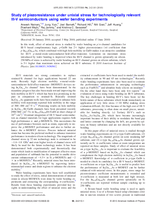
(a)
(b)
A 0 2Ga0 8As 50Å
W1
242110 2
8
% Enhancemen
n0 2Ga0 8As 120Å
W2
Strain gauge
III-V
GaAs 1000Å
Silicon/Steel
d1
d2
four point bending setups, and has been able to achieve up to
700 MPa stress in silicon MOSFETs.13 For measurements on
III-V substrates the III-V piece is glued using epoxy to a
silicon substrate/steel plate for bending, while for the III-V
grown expitaxially on Si substrate the measurement is done
directly. A strain gauge is mounted on top of the III-V sample
to ascertain the amount of stress transferred 关Fig. 1共a兲兴.
-coefficients are extracted at room temperature for longitudinal stress along the direction of current flow. All results are
reported for current flow along 具110典 direction on 共001兲 wafer orientation, which is the standard channel/wafer orientation for present day devices. Transfer length method 共TLM兲
test structures 关Fig. 1共b兲兴 are used for measuring the change
in conductivity.14 The measurements were done at low electric field and current density of ⱕ1 A / mm ruling out any
hot carrier effects. Use of TLM test structures allows measurement of resistivity change in the semiconductor independent of change in the contact resistance. I-V characteristics
are measured using a Keithley 4200 semiconductor parameter analyzer. The measurements were verified to be fully
reversible on the removal of stress ruling out any residual
stress after the measurement.
The most effective empirical method to predict device
behavior under stress is by measuring -coefficients. Table I
summarizes the L values for n- and p-type Si and Ge15
which correspond to piezoresistance for 具110典 channel direction on 共001兲 substrate orientation with the stress applied
longitudinal to the current flow, measured at room temperature 关Eq. 共1兲兴.
⌬
;
P
J关110兴 储 P关110兴.
4
2
FIG. 1. 共Color online兲 共a兲 Cartoon depicting the measurement setup 共b兲
TLM structures with varying widths and distance between the contact pads
are used to extract the conductivity and its change with stress.
L =
6
'V/V (A)
Al0.2Ga0.8As 200Å
共1兲
Although the L values extracted on bulk 共Table I兲 do not
account for the effect of surface confinement that occurs in a
MOSFET device, the results on silicon have been widely
used to calibrate strain models and correctly predict
MOSFET current enhancement under stress.16 It has further
Ge 400Å
0
Si Substrate
F G 2 Co o on ne S ack de a s
on s con e
L nea enhancemen
up o 250 MPa was ach eved w hou
max mum s ess ach eved on a
V
0
50 100 150 200 250
S ess MPa
o he n n Ga As channe g own
n conduc v y w h un ax a ens on
c ack ng wh ch s 5⫻ h ghe han he
subs a e
been shown that -coefficients have weak dependence
on doping density and have a strong dependence on
temperature.17
We first discuss the results on III-V substrates, i.e., 共1兲
p-type GaSb substrate and 共2兲 p-type In0.53Ga0.47As expitaxially grown on InP. It is observed that when these samples are
glued to silicon and stress is applied using the bending setup
the maximum achieved stress is ⬃35 MPa before cracks
start to appear on the top surface of the sample. High stress
transfer in silicon pieces has been reported by adhering onto
1.2-mm-thick steel plate;18 we found that this approach
slightly improves the maximum stress transfer to ⬃50 MPa
probably because of the better adhesion of the epoxy to
steel. 4.1%/2% increase in conductivity is measured for
p-GaSb/ p-In0.53Ga0.47As with 50 MPa uniaxial compression.
The corresponding L values are 0.82/GPa for p-GaSb and
0.40/GPa for p-In0.53Ga0.47As. -coefficient for p-type GaSb
is found to be ⬎2⫻ higher as compared to p-type
In0.53Ga0.47As 共Table I兲.
Figure 2 describes the stack for III-V grown on silicon
substrate and the enhancement with uniaxial tension. The
enhancement is observed to be linear with applied stress and
no saturation is seen until the maximum achievable stress of
250 MPa. A 7.5% increase in conductivity is observed with
250 MPa tension corresponding to a L value of ⫺0.30/GPa.
We believe this value could be slightly better and is limited
by the misfit defects in these samples 共observed in cross
section transmission electron microscope analysis兲, which
are introduced at the Si/Ge interface due to the thickness of
the Ge layers exceeding the critical thickness and propagate
through the GaAs buffer 共Fig. 2兲. A better engineering of the
TABLE I. Summary of the piezoresistance coefficient L extracted from previous papers and this work for
current flow along 具110典 direction on a 共001兲 substrate. A + value corresponds to enhancement with compression while ⫺ value means enhancement with tension.
具110典共001兲
n-Si/p-Si
n-Ge/p-Ge
p-GaSb
p-In0.53Ga0.47As on InP
n-In0.20Ga0.80As on silicon
96 242110 2010
L = ⌬ / P =共11 + 22 + 44兲 / 2
共/GPa兲
Remarks
−0.31/ +0.71
−0.72/ +0.48
+0.82⫾ 0.08
+0.40⫾ 0.07
−0.31⫾ 0.02
13 and 15
15 and 26
This work, max stress= 50 MPa
This work, max stress= 50 MPa
This work, max stress= 250 MPa
�(a)
3
3x10
Si
(b)
Ge
In0.2Ga0.8As
Si
Ge
GaSb
In0.53Ga0.47As
3
2x10
2.5x10
4
2.0x10
4
1.5x10
4
1.0x10
4
5.0x10
3
2
2
�h �cm /Vs)
Appl. Phys. Lett. 96, 242110 共2010兲
Nainani et al.
�e �cm /Vs)
242110-3
3
1x10
2
1
0 0
Uniaxial Compression (GPa)
1
2
Uniaxial Tension (GPa)
FIG. 3. 共Color online兲 Predicted mobility enhancement in p-type 共a兲 and
n-type 共b兲 semiconductors using extracted piezoresistance coefficients.
Among III-V candidates GaSb appears promising for hole mobility, while
InGaAs maintains it superiority in electron mobility.
growth process should be able to further improve the enhancement with stress in these samples.
To put the results in perspective preliminary predictions
are made for electron and hole mobility under uniaxial stress
for the different channel materials 共Fig. 3兲 using the unstrained mobility values19 and the extracted L values. Ge
which has high unstrained hole mobility of 1900 cm2 / V s
and L value +0.48/ GPa maintains highest hole mobility on
application of stress. Among the III-V p-MOSFET candidates GaSb with unstrained hole mobility of 850 cm2 / V s
and a high L value +0.82/ GPa looks promising. For
n-MOSFET InGaAs maintains its superiority in electron mobility with uniaxial tension.
Finally, we make some comments on the results obtained. Recently hole mobility and its enhancement with
strain has been studied for III-V semiconductors using band
structure obtained from k.p method.20,21 We find our predictions to be in good qualitative agreement with the modeling
results in Refs. 20 and 21. The higher -coefficient for
p-type GaSb as compared to InGaAs can be related to the
fact that valence bands in III-V semiconductors derive primarily 2p orbital of the group V element.20,22 Hence GaAs/
InAs and their tertiaries have similar valence band structure
and comparable hole mobility 共similarly InSb/GaSb and their
tertiaries兲, while the valence band structure and their properties are considerably different between the arsenides and antimonides. It is important to mention that while n-type GaAs
has larger electron mobility and higher -coefficient than Si,
saturation of enhancement with uniaxial strain was observed
by Suthram et al.23 at very low stress of 共⬃100 MPa兲. This
saturation behavior was attributed to the repopulation of the
carriers between the ⌫ & L valleys with stress.23,24 Although
InxGa1−xAs has slightly higher energy separation between the
⌫ & L valley as compared to GaAs 共450/360meV in
In0.53Ga0.47As/ In0.30Ga0.70As versus 280 meV in GaAs兲,25 a
more detailed analysis is needed to predict the performance
enhancement in InGaAs n-MOSFET under high stress.
In summary, we have extracted piezoresistance coefficients by wafer bending for candidates for III-V based
View publication stats
MOSFETS. The extracted values will be useful for the performance prediction and modeling under stress. The limitation on amount of stress possible by wafer bending on III-V
substrates is lifted by growing III-V epitaxially on silicon.
Enhancement with upto 250 MPa stress is demonstrated
which is 5⫻ higher than the maximum stress possible on a
III-V substrate.
1
Y. Xuan, T. Shen, M. Xu, Y. Q. Wu, and P. D. Ye, Tech. Dig. - Int.
Electron Devices Meet. 2008, 371.
2
T. J. Drummond, T. E. Zipperian, I. J. Fritz, J. E. Schirber, and T. A. Plut,
Appl. Phys. Lett. 49, 461 共1986兲.
3
A. M. Kusters, A. Kohl, V. Sommer, R. Muller, and K. Heime, IEEE
Trans. Electron Devices 40, 2164 共1993兲.
4
A. Nainani, S. Raghunathan, D. Witte, M. Kobayashi, T. Irisawa, T. Krishnamohan, K. Saraswat, B. R. Bennett, M. G. Ancona, and J. Brad Boos,
Tech. Dig. - Int. Electron Devices Meet. 2009, 857.
5
N. Kusunoki, N. Yasutake, M. Awano, I. Mizushima, H. Yoshimura, S.
Yamada, and F. Matsuoka, Proceedings of Simulation of Semiconductor
Processes and Devices 共SISPAD兲 2007, Vol. 12, p. 121.
6
G. Sun, Y. Sun, T. Nishida, and Scott E. Thompson, J. Appl. Phys. 102,
084501 共2007兲.
7
H. C. Chin, X. Gong, X. Liu, and Y. C. Yeo, IEEE Electron Device Lett.
30, 805 共2009兲.
8
B. M. Haugerud, L. A. Bosworth, and R. E. Belford, J. Appl. Phys. 94,
4102 共2003兲.
9
S. E. Thompson, M. Armstrong, C. Auth, S. Cea, R. Chau, G. Glass, T.
Hoffman, J. Klaus, M. Zhiyong, B. Mcintyre, A. Murthy, B. Obradovic, L.
Shifren, S. Sivakumar, S. Tyagi, T. Ghani, K. Mistry, M. Bohr, and Y.
El-Mansy, IEEE Electron Device Lett. 25, 191 共2004兲.
10
S. Suthram, M. M. Hussain, H. R. Harris, C. Smith, H.-H. Tseng, R.
Jammy, and S. E. Thompson, IEEE Electron Device Lett. 29, 480 共2008兲.
11
K. Uchida, R. Zednik, C. Lu, H. Jagannathan, J. McVittie, and Y. Nishi,
Tech. Dig. - Int. Electron Devices Meet. 2004, 229.
12
L. Xia and J. A. del Alamo, Appl. Phys. Lett. 95, 243504 共2009兲.
13
S. Suthram, J. C. Ziegert, T. Nishida, and S. E. Thompson, IEEE Electron
Device Lett. 28, 58 共2007兲.
14
D. K. Schroder, Semiconductor Material and Device Characterization, 3rd
ed. 共Wiley, New York, 2005兲, Chap. 3.
15
C. S. Smith, Phys. Rev. 94, 42 共1954兲.
16
Technical Manual, Sentaurus Tool Chain from Synopsis.
17
Y. Kanda, IEEE Trans. Electron Devices 29, 64 共1982兲.
18
R. He and P. Yang, Nat. Nanotechnol. 1, 42 共2006兲.
19
Semiconductor Parameter Database: http://www.ioffe.ru/SVA/NSM/
Semicond/.
20
A. Nainani, D. Kim, T. Krishnamohan, and K. Saraswat, Proceedings of
Simulation of Semiconductor Processes and Devices (SISPAD) 共IEEE,
New York, 2009兲, p. 1.
21
Y. Zhang and M. V. Fischetti, Proceedings of the International Workshop
on Computational Electronics (IWCE) 共IEEE, New York, 2009兲, p. 1.
22
G. Bastard, Wave Mechanics Applied to Semiconductor Heterostructures,
共Wiley, New York, 1988兲.
23
S. Suthram, Y. Sun, P. Majhi, I. Ok, H. Kim, H. R. Harris, N. Goel, S.
Parthasarathy, A. Koehler, T. Acosta, T. Nishida, H.-H. Tseng, W. Tsai, J.
Lee, R. Jammy, and S. E. Thompson, Proceedings of the 2008 Symposium
on VLSI Technology 共IEEE, New York, 2008兲, p. 182.
24
Y. Sun, S. E. Thompson, and T. Nishida, J. Appl. Phys. 101, 104503
共2007兲.
25
W. Porod and D. K. Ferry, Phys. Rev. B 27, 2587 共1983兲.
26
M. Kobayashi, T. Irisawa, B. M. Kope, Y. Sun, K. Saraswat, H.-S. P.
Wong, P. Pianetta, and Y. Nishi, Proceedings of the 2009 Symposium on
VLSI Technology 共IEEE, New York, 2009兲, p. 76.,
�
 Joel Barnett