WO2004013715A1 - Method, system, and medium for handling misrepresentative metrology data within an advanced process control system - Google Patents
Method, system, and medium for handling misrepresentative metrology data within an advanced process control system Download PDFInfo
- Publication number
- WO2004013715A1 WO2004013715A1 PCT/US2003/023964 US0323964W WO2004013715A1 WO 2004013715 A1 WO2004013715 A1 WO 2004013715A1 US 0323964 W US0323964 W US 0323964W WO 2004013715 A1 WO2004013715 A1 WO 2004013715A1
- Authority
- WO
- WIPO (PCT)
- Prior art keywords
- data point
- outlier
- current data
- previous
- measurements
- Prior art date
- Legal status (The legal status is an assumption and is not a legal conclusion. Google has not performed a legal analysis and makes no representation as to the accuracy of the status listed.)
- Ceased
Links
Classifications
-
- G—PHYSICS
- G05—CONTROLLING; REGULATING
- G05B—CONTROL OR REGULATING SYSTEMS IN GENERAL; FUNCTIONAL ELEMENTS OF SUCH SYSTEMS; MONITORING OR TESTING ARRANGEMENTS FOR SUCH SYSTEMS OR ELEMENTS
- G05B23/00—Testing or monitoring of control systems or parts thereof
- G05B23/02—Electric testing or monitoring
- G05B23/0205—Electric testing or monitoring by means of a monitoring system capable of detecting and responding to faults
- G05B23/0218—Electric testing or monitoring by means of a monitoring system capable of detecting and responding to faults characterised by the fault detection method dealing with either existing or incipient faults
- G05B23/0221—Preprocessing measurements, e.g. data collection rate adjustment; Standardization of measurements; Time series or signal analysis, e.g. frequency analysis or wavelets; Trustworthiness of measurements; Indexes therefor; Measurements using easily measured parameters to estimate parameters difficult to measure; Virtual sensor creation; De-noising; Sensor fusion; Unconventional preprocessing inherently present in specific fault detection methods like PCA-based methods
-
- G—PHYSICS
- G05—CONTROLLING; REGULATING
- G05B—CONTROL OR REGULATING SYSTEMS IN GENERAL; FUNCTIONAL ELEMENTS OF SUCH SYSTEMS; MONITORING OR TESTING ARRANGEMENTS FOR SUCH SYSTEMS OR ELEMENTS
- G05B15/00—Systems controlled by a computer
- G05B15/02—Systems controlled by a computer electric
Definitions
- the present invention relates to improved feedback controllers designed for manufacturing semiconductor devices.
- the feedback controllers of the present invention include features to detect erroneous data points and to prevent those data points from affecting the operation of the feedback controllers.
- An example of a feedback controller system 100 includes a tool 103 and a feedback controller 107 coupled each other.
- the tool 103 can be one or any combination of semiconductor-manufacturing tools such as a chemical mechanical planarization (CMP) tool, a depositor, an etcher, etc.
- CMP chemical mechanical planarization
- the tool 103 receives wafers as input 101 and processes them according to a set of control parameters 109, e.g., recipes received from the controller 107.
- the processed wafers are referred to as outputs 105. Examples of processes are depositing a new layer of film, etching a layer, etc.
- one or more metrology stations make measurements on the processed wafer.
- the measurements are communicated to the controller 107.
- the controller 107 compares the measurements to predicted values calculated previously. Based on the comparison, the controller 107 makes adjustments to the control parameters 109. For example, if the thickness of a newly deposited layer is outside of a desired range when the measurement is compared with the predicted value, the controller 107 adjusts one or more of the control parameters 109, e.g., the amount of gas flow, the length of processing time, etc., to deposit a thinner film on the next wafer.
- the tool 103 receives another wafer and processes the wafer using the adjusted control parameters.
- the performance of the feedback controller depends on, in part, receiving accurate measurements from the metrology stations. When inaccurate or erroneous measurements are received, the feedback controller needs to identify such measurements and have a mechanism to prevent such measurements from affecting the operation. In conventional feedback controllers, no robust mechanism was provided to address erroneous measurements. When erroneous measurements are entered repeatedly to the controller 107, they cause increased defects, low yields, or both in devices formed on processed wafers.
- Embodiments of the present invention advantageously identify erroneous measurements and prevent the erroneous measurements from being input to a feedback controller.
- embodiments of the present invention provide a system, method and medium for initially identifying erroneous data points and preventing them from affecting the operation of the feedback controller.
- Embodiments of the present invention include features for receiving data points relating to an output of the tool.
- the data points include a current data point and at least one previous data point. The at least one previous data point is received before the current data point.
- Embodiments of the present invention also include features for determining whether the current data point is an erroneous outlier by comparing the current data point to a statistical representation of the at least one previous data point, and based on whether the at least one previous data point was also an outlier. Embodiments of the present invention further include features for disregarding the current data point in calculating a feedback value of the feedback control mechanism if the current data point is determined as an erroneous outlier.
- FIG. 1 is a block diagram illustrating a conventional feedback control system
- FIG. 2 is a graph illustrating an example outlier data point
- FIG. 3 is a graph illustrating an example step change
- FIG. 4 is a block diagram illustrating a feedback controller that includes an optimizer and an estimator according to embodiments of the present invention
- FIG. 5 is a flow chart illustrating high level features of the estimator according to embodiments of the present invention.
- FIG. 6 is a flow chart illustrating features of the estimator with respect to determining an outlier according to embodiments of the present invention
- FIG. 7 is a flow chart illustrating features of the estimator with respect to adjusting measurements according to embodiments of the present invention
- FIGs. 8 A and 8B are flow charts illustrating features of overall sequence of steps according to embodiments of the present invention.
- FIG. 9 is a graph illustrating example measurement values processed according to embodiments of the present invention.
- FIG. 10 is a block diagram representation of a computer within which an example embodiment of the feedback controller can operate according to embodiments of the present invention.
- a feedback system for a semiconductor manufacturing tool typically includes a metrology station (which can be internal to or external of the tool) to make measurements on one or more characteristics of outputs (e.g., processed wafers) of the tool and a feedback controller to change the operation of the tool based on data points (where a data point is calculated from or equivalent to one or more measurements of a wafer or wafers).
- a metrology station which can be internal to or external of the tool
- a feedback controller to change the operation of the tool based on data points (where a data point is calculated from or equivalent to one or more measurements of a wafer or wafers).
- Various embodiments of the present invention relate to feedback controllers that include features for identifying outlier data points (i.e., data points that are substantially different from one or more previous data points), for differentiating the outlier data points into erroneous outlier data points and non-erroneous outlier data points (e.g., outliers representing a change in the status of the tool), and for removing the erroneous data points from affecting the operation of the feedback controller and its tool.
- outlier data points i.e., data points that are substantially different from one or more previous data points
- non-erroneous outlier data points e.g., outliers representing a change in the status of the tool
- these outlier measurements are identified and removed before calculating any data points for the wafer. These embodiments are described in connection with FIG. 7. In at least some embodiments of the present invention, portions or all of the features of the above-mentioned embodiments relating to identifying and removing outliers from measurements and data points can be combined into one system. These embodiments are described in connection with FIGs. 8A-8B.
- an outlier is a data point that is significantly different from previous data points.
- the significance of the difference can be measured in terms of statistics, e.g., average, median, standard deviation, etc.
- An outher data point may indicate that a change has occurred in the tool and that a response by the feedback controller may be required (e.g., adjusting control parameters).
- an outlier data point may indicate that the measurements made by the metrology station are erroneous (i.e., an erroneous outlier data point). In such a case, the erroneous outlier data point is removed from affecting the operation of the feedback controller.
- a black line 201 depicts a trace of differences between data points and their respective predicted values in a sequence of processed wafers.
- the predicted values are calculated based on, in part, previous data points.
- difference values, F(k) of the processed wafers are shown.
- Processed wafer 20 has its difference value at 1, while wafers 1-19 and 21-40 have their difference values at zero.
- the data point for wafer 20 depicted in FIG. 2 misrepresents or incorrectly characterizes the processes that took place in the tool because the difference value jumps to 1 for wafer 20 and drops back to zero. It may also represent an error in calculating the data point that was the basis for calculating the difference value.
- Such a data point is preferably treated as an erroneous input. Accordingly, it is desirable to prevent such a data point from being input to the feedback controller.
- FIG. 3 a similar change occurs at processed wafer 20, but the difference values stay at 1 for wafers 21-40. In such a case, the difference value for wafer 20 most likely represents the leading edge of a change rather than an erroneous outlier.
- the change illustrated in FIG. 3 contains relevant information regarding the processes that took place in the tool. Accordingly, it is desirable to input the data point at the leading edge of the change to the feedback controller in order to make appropriate adjustments.
- embodiments of the present invention include, among other features, a tool 401, one or more metrology stations 403, and a feedback controller 406 that includes an estimator 405 and an optimizer 407 as illustrated in FIG. 4.
- the tool 401 is similar to that described above in connection with FIG. 1.
- the metrology stations 403 (which can be part of, or external to, tool 401) are configured to make one or more measurements on the processed wafers.
- the measurements can be of different categories, e.g., the thickness of deposited films, various features of transitions, etc.
- the metrology stations 403 can also make one or more measurements for each category measurement. For instance, the metrology stations 403 can measure the thickness of a wafer at multiple points on a processed wafer.
- the values of the measurements made by the metrology stations 403 are communicated to the controller 406.
- the estimator 405 Upon receiving the measurement values, the estimator 405 calculates one or more data points from the measurements.
- the estimator 405 is configured to improve prediction capabilities of the controller 406 based on new information, e.g., data points, etc.
- the estimator 405 determines if the new data point is significantly different from the predicted value, and can thus be considered a "candidate" outlier (step 503). If so, the data point is designated as a candidate outlier (step 504). It is called a candidate because whether the outlier is an erroneous data point or a data point representing a change is determined later. If the data point is not a candidate outlier, then the estimator 405 calculates and communicates a feedback value of the data point to the optimizer 407 (step 509).
- the feedback value is a value proportional to the difference (if any) between the value of the data point and the predicted value calculated by the controller 406.
- the optimizer 407 uses the feedback value in calculating a new set of control parameters.
- the optimizer 407 is configured to produce control parameters in an optimal way
- the data point is a candidate outlier, and the previous data point was not marked as a candidate outlier (as determined by step 505 in processing the previous data point), the data point is most likely an erroneous data point (i.e., an erroneous outlier) similar to the one depicted in FIG. 2. As such, no feedback value is communicated to the optimizer 407 (step 511(a)). In other words, such a data point is removed from affecting the operation of the optimizer 407. It follows that if the previous data point is not a candidate outlier, the data point is a candidate, and a subsequent data point is not a candidate, then the data point is an erroneous data point.
- the estimator 405 determines if two or more previous data points were marked as outliers instead of just one previous data point. In such embodiments, if the two or more previous data points were not marked as outliers, the data point is designated as an erroneous outlier. Once again, no feedback value is communicated to the optimizer 407. When no feedback value is communicated, the optimizer 407 can use the previous set of control parameters in controlling the tool 401.
- a threshold test is first performed. In these embodiments of the present invention, even if the new data point is determined to be a candidate outlier, if the difference between the data point and the predicted value falls below/above the threshold value, then a feedback value is communicated to the optimizer 407 to be used in calculating the control parameters. It should be noted that the threshold can also be a range as well.
- the estimator 405 determines that the previous data point was also an outlier (or a candidate outlier), this condition is similar to the one depicted in FIG. 3 because the change that took place with the previous data point continues in the current data point. In such a case, the feedback value of the previous data point would not have been communicated to the optimizer 407 for the previous data point, when it should have been because it represented a change. Hence, the estimator 405 first calculates the feedback value of the previous data point, and the feedback value of the new data point is then calculated. The latter value is communicated to the optimizer 407 to be used in calculating the control parameters (step 507).
- the optimizer 407 is configured to receive any number of feedback values from the estimator 405. More specifically, when it receives the feedback values from the estimator 405, the optimizer 407 calculates a new set of control parameters, hi calculating the new set of control parameters, the optimizer 407 may simply make adjustments to the previous set of control parameters based on the feedback values received.
- a statistical filter in order to determine if a data point is a candidate outlier, a statistical filter is used.
- an exponentially-weighted moving average (EWMA) filter is used.
- other types of filters can also be used, e.g., finite- impulse response, infinite-impulse response, or wavelet-based filters.
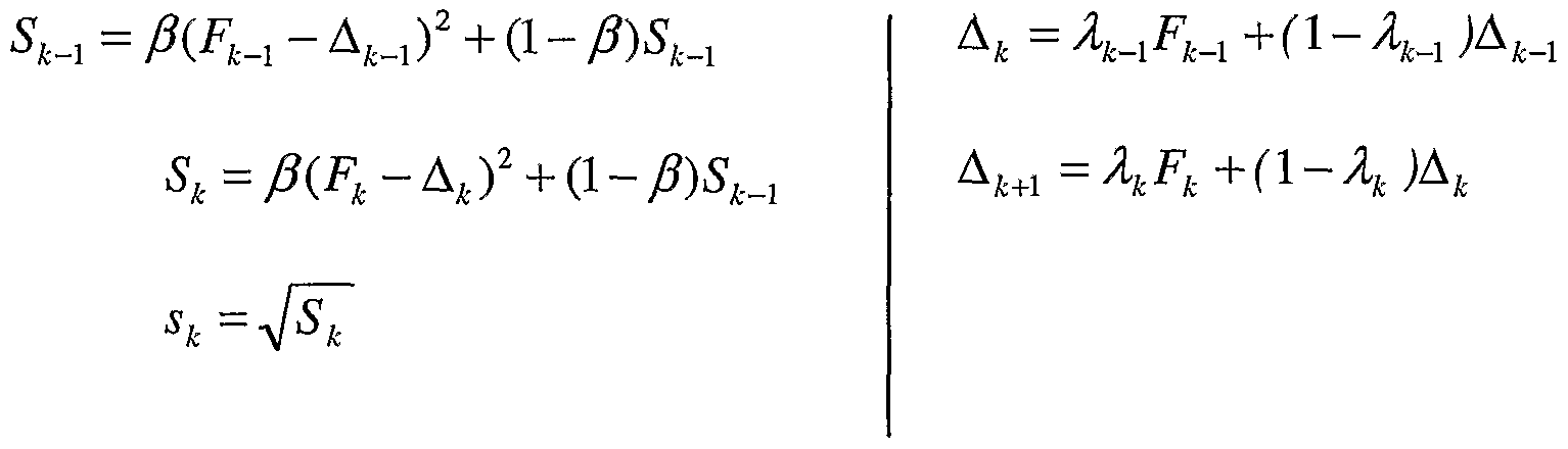
- the exponentially-weighted moving average for variance of prediction value can be expressed as:
- P is a coefficient used for the EWMA filter
- k is the difference between the data point and predicted value for wafer k, and it can be actual predicted expressed as ⁇ k ⁇ 1 ⁇ k ⁇ l , where
- V k-l is the actual value measured at time/wafer k-l; and predicted yk ⁇ l is the predicted value at time/wafer k-l;
- k is a feedback value for time k, k .
- One example set of equations for calculating a feedback value is as follows:
- * is a coefficient used for the ⁇ WMA-based filter, which is optionally a function of ⁇ time and/or other processing events (the value of k may also be set to be a function of wafer number, distance from target or another type of process related event such as the beginning of a new lot or change in process condition); and
- outlier coefficient is a value called outlier coefficient, which can be set to a certain value, e.g., 0.1.
- the feedback value is updated when the difference between k and the feedback value is greater than a specified threshold value, " k . This places a limit on the size of adjustments the optimizer 407 may make.
- the data point is marked as a candidate outlier if ]F k — A k
- K is set to a certain value, e.g., 3.
- the actual marking is designated as follows:
- a state indicates whether the previous data point was marked as an outlier (step 603): if the data point is not a candidate outlier, the state is set to 'regular'; if the data point is a candidate outlier and the previous data point was not marked as an outlier, then the data point is meanwhile regarded as an outlier, and the state is set to 'ignore'; and if the data point is a candidate outlier and the previous data point was not marked as an outlier, both points are used for the filter calculations, and the state is set to 'two'.
- the following is a set of pseudo codes that capture the above-described feature of setting the state of the data point:
- the estimator 405 performs the steps described in connection with FIG. 5 in calculating the feedback value. In addition, the estimator 405 also calculates various values of the exponentially- weighted moving average filter and its variance to be used when the next data point arrives:
- the following equations calculate the values for the previous and the present data points (steps 605 and 607) and feedback values.
- a M ⁇ k F k + (l - ⁇ k )A k s k - V $k else
- the outlier measurements may occur due to problems related to the metrology stations such as misalignment of the measurement coordinates or due to physical phenomena such as the presence of particles. These problems negatively influence the measurement accuracy. Therefore, it is desirable to identify and remove outlier measurements before they are used in calculating data points.
- measurements and information needed to determine outliers are resource specific. This means the information is retained based upon which specific tool or chamber the wafer was processed. Also, the values for the statistical analysis are advantageously maintained as relative values rather than as absolute values.
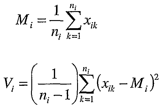
- the estimator 405 receives a number of measurements from one or more of metrology stations 403 (step 701). In particular, the estimator 405 retains sufficient information to determine in which specific tool or chamber the wafer was processed. After receiving the measurements from the metrology stations, the estimator 405 calculates their mean and variance values (step 703). In particular, the mean and variance are expressed as:
- data sets are designated as sety and run/wafer i ;
- Vj is the variance.
- the mean and variance values can be calculated using a portion or all of the population of the measurements collected for the run/wafer i.
- “FLAG” is set to one (step 709). If the scaling is not performed, the "FLAG" register and the scaled variance are set to zero (step 707). The following is a set of equations describing these features:
- the estimator 405 then calculates a filtered estimate of the Z), and V,- , which are designated j f andV as i* 1 !+1 , respectively (step 711).
- the estimator 405 which receives a reliability level from a user (step 715), calculates a sigma coefficient Kf, based on the reliability level.
- the estimator 405 also calculates the median, R jt , of the measurement values (step 717). Using the median, R jh for run/wafer i data set , the sigma coefficient
- the estimator 405 calculates an interval (step 719).
- the estimator 405 calculates the average of the set of measurement values that fall within the interval (step 721).
- the estimator 405 replaces all measurements in set j that lie outside the interval with the average value, and sets these points to be outliers (step 723).
- the estimator 405 then recalculates and stores the filtered estimate values (step 725).
- the value of ⁇ is configurable in a graphical user interface.
- FIGs. 8A and 8B are identical to FIGs. 8A and 8B.
- measurements that include the value of goodness-of-fit are received from the metrology stations 403 (step 801).
- the estimator 405 conducts a measurement outlier screening (step 803). This step is similar to the steps described above in connection with calculating an interval for the measurements; however, in these embodiments, the GOF and statistical outlier limits for specifically controlled output are provided from memory (805). If all measurements are outside the interval, then the measurements are not used in calculating a feedback value (step 809). If all measurements are not outside the interval, then the estimator 405 calculates the average value of the measurements that fall within the interval (step 811). The estimator 405 then updates statistical information (step 813), which can then be stored as an array of statistical information for specific controlled output from previous runs (step 815).
- the average value calculated in step 811 is used as a data point.
- the estimator 405 performs a data point outlier screen step, which determines whether the data point is a candidate outlier similar to the steps described above in connection with FIGs. 5-6. Based on step 817, the estimator 405 determines if the data point is an outlier. If it is an outlier, then the data point is not used in calculating a feedback value (step 825). A state of the data point is determined similar to the steps described above in connection with steps 603, 605 and 607 (step 821). The estimator 405 stores the current state of the data point (step 823).
- the estimator 405 performs a feedback value screening (step 827), which is similar to the threshold test described above in connection with FIGs. 5-6. Based on the feedback value screening, the estimator 405 determines whether the feedback value is within noise limits (step 829). If the feedback value is within the noise limits, then the feedback value is not communicated to the optimizer 407 (step 831). Otherwise, the feedback value is communicated to the optimizer (step 833). Regardless of whether the feedback value falls within the noise limits, the estimator updates statistical information of relating to the data point (step 835). The resulting values are stored as statistical information for specific controlled output from previous runs to be used in performing the feedback outlier screening (step 837) and noise screening steps (step 839).
- each data point represents a wafer being processed by Chemical Vapor Deposition (CVD).
- a metrology station collects thickness measurements of the processed wafers. For the measurements within normal operation, the average values of the measurements are used as the data points.
- the measurements are out of range 907 (e.g., above a threshold value set to detect catastrophic cases), then the tool is halted and a message (e.g., an e-mail message and/or page) is sent to an operator.
- a message e.g., an e-mail message and/or page
- such a set of measurements is not used in calculating a feedback value.
- one of the measurements is out of an interval (e.g., 905), then the measurement is replaced with the average of the measurements within the interval and the filter values are stored.
- Embodiments of the present invention can be implemented as a set of computer executable codes (e.g., computer programs), implemented using computer hardware, or any combination of them.
- embodiments of the present invention are described in terms of various flow charts as shown in FIGs. 5-8A, B.
- Various acts depicted in the flow charts can be implemented as codes in computer programs or using computer hardware.
- FIG. 10 illustrates a block diagram of such embodiments.
- a bus 1056 serves as the main information highway interconnecting various components.
- CPU 1058 is the central processing unit, performing calculations and logic operations required to execute the processes of the present invention as well as other programs.
- Read only memory (ROM) 1060 and random access memory (RAM) 1062 constitute the main memory.
- Disk controller 1064 interfaces one or more disk drives to the system bus 1056. These disk drives are, for example, floppy disk drives 1070, or CD ROM or DVD (digital video disks) drives 1066, or internal or external hard drives 1068. These various disk drives and disk controllers are optional devices.
- a display interface 1072 interfaces display 1048 and permits information from the bus 1056 to be displayed on display 1048. Communications with external devices such as the other components of the system described above, occur utilizing, for example, communication port 1074.
- Optical fibers and/or electrical cables and/or conductors and/or optical communication (e.g., infrared, and the like) and/or wireless communication (e.g., radio frequency (RF), and the like) can be used as the transport medium between the external devices and communication port 1074.
- Peripheral interface 1054 interfaces the keyboard 1050 and mouse 1052, permitting input data to be transmitted to bus 1056.
- the analyzer also optionally includes an infrared transmitter and/or infrared receiver.
- Infrared transmitters are optionally utilized when the computer system is used in conjunction with one or more of the processing components/stations that transmits/receives data via infrared signal transmission.
- the computer system may also optionally use a low power radio transmitter 1080 and/or a low power radio receiver 1082.
- the low power radio transmitter transmits the signal for reception by components of the production process, and receives signals from the components via the low power radio receiver.
- the low power radio transmitter and/or receiver are standard devices in the industry.
- the analyzer is optionally suitably equipped with any multitude or combination of processors or storage devices.
- the various embodiments may be replaced by, or combined with, any suitable processing system operative in accordance with the principles of embodiments of the present invention, including sophisticated calculators, and hand-held, laptop/notebook, mini, mainframe and super computers, as well as processing system network combinations of the same.
- Computer readable memory medium stores computer readable code or instructions.
- the medium may be used with disk drives illustrated in FIG. 10.
- memory media such as a CD ROM, a digital video disk, or floppy disks will contain, for example, a multi-byte locale for a single byte language and the program information for controlling the modeler to enable the computer to perform the functions described herein.
- ROM 1060 and/or RAM 1062 illustrated in FIG. 10 can also be used to store the program information that is used to instruct the central processing unit 1058 to perform the operations associated with various automated processes of the present invention.
- suitable computer readable media for storing information include magnetic, electronic, or optical (including holographic) storage, some combination thereof, etc.
Landscapes
- Engineering & Computer Science (AREA)
- Physics & Mathematics (AREA)
- General Physics & Mathematics (AREA)
- Automation & Control Theory (AREA)
- General Engineering & Computer Science (AREA)
- Testing Or Measuring Of Semiconductors Or The Like (AREA)
- Exposure And Positioning Against Photoresist Photosensitive Materials (AREA)
Abstract
Description

Claims

Priority Applications (3)
| Application Number | Priority Date | Filing Date | Title |
|---|---|---|---|
| JP2004526262A JP2005535130A (en) | 2002-08-01 | 2003-08-01 | Methods, systems, and media for handling misrepresented measurement data in modern process control systems |
| EP03767017A EP1546828A1 (en) | 2002-08-01 | 2003-08-01 | Method, system, and medium for handling misrepresentative metrology data within an advanced process control system |
| AU2003254283A AU2003254283A1 (en) | 2002-08-01 | 2003-08-01 | Method, system, and medium for handling misrepresentative metrology data within an advanced process control system |
Applications Claiming Priority (2)
| Application Number | Priority Date | Filing Date | Title |
|---|---|---|---|
| US39969502P | 2002-08-01 | 2002-08-01 | |
| US60/399,695 | 2002-08-01 |
Publications (1)
| Publication Number | Publication Date |
|---|---|
| WO2004013715A1 true WO2004013715A1 (en) | 2004-02-12 |
Family
ID=31495751
Family Applications (1)
| Application Number | Title | Priority Date | Filing Date |
|---|---|---|---|
| PCT/US2003/023964 Ceased WO2004013715A1 (en) | 2002-08-01 | 2003-08-01 | Method, system, and medium for handling misrepresentative metrology data within an advanced process control system |
Country Status (7)
| Country | Link |
|---|---|
| US (1) | US6999836B2 (en) |
| EP (1) | EP1546828A1 (en) |
| JP (1) | JP2005535130A (en) |
| KR (1) | KR20050026099A (en) |
| CN (1) | CN100351725C (en) |
| AU (1) | AU2003254283A1 (en) |
| WO (1) | WO2004013715A1 (en) |
Cited By (3)
| Publication number | Priority date | Publication date | Assignee | Title |
|---|---|---|---|---|
| JP2005331944A (en) * | 2004-05-18 | 2005-12-02 | Xerox Corp | Method and apparatus for implementing statistical process control (spc) in printing environment |
| US9581996B2 (en) | 2011-04-01 | 2017-02-28 | Hitachi Kokusai Elecric Inc. | Apparatus, method, and computer-readable medium for managing abnormality data measured in the substrate manufacturing process |
| CN111183510A (en) * | 2017-10-05 | 2020-05-19 | 应用材料公司 | Error detection classification |
Families Citing this family (47)
| Publication number | Priority date | Publication date | Assignee | Title |
|---|---|---|---|---|
| US6863771B2 (en) * | 2001-07-25 | 2005-03-08 | Micron Technology, Inc. | Differential pressure application apparatus for use in polishing layers of semiconductor device structures and methods |
| US6917849B1 (en) * | 2002-12-18 | 2005-07-12 | Advanced Micro Devices, Inc. | Method and apparatus for predicting electrical parameters using measured and predicted fabrication parameters |
| US20060129257A1 (en) * | 2004-12-13 | 2006-06-15 | Taiwan Semiconductor Manufacturing Co., Ltd. | Novel method and apparatus for integrating fault detection and real-time virtual metrology in an advanced process control framework |
| US7477958B2 (en) * | 2005-05-11 | 2009-01-13 | International Business Machines Corporation | Method of release and product flow management for a manufacturing facility |
| JP4417897B2 (en) * | 2005-09-14 | 2010-02-17 | 富士通マイクロエレクトロニクス株式会社 | Manufacturing data analyzing method and manufacturing data analyzing apparatus |
| US7359759B2 (en) * | 2005-10-31 | 2008-04-15 | Taiwan Semiconductor Manufacturing Company | Method and system for virtual metrology in semiconductor manufacturing |
| US7200523B1 (en) * | 2005-11-30 | 2007-04-03 | Taiwan Semiconductor Manufacturing Company, Ltd. | Method and system for filtering statistical process data to enhance process performance |
| EP1793296A1 (en) * | 2005-12-05 | 2007-06-06 | Insyst Ltd. | An apparatus and method for the analysis of a process having parameter-based faults |
| US7292959B1 (en) * | 2006-01-30 | 2007-11-06 | Advanced Mirco Devices, Inc. | Total tool control for semiconductor manufacturing |
| US7522968B2 (en) * | 2006-07-10 | 2009-04-21 | Applied Materials, Inc. | Scheduling method for processing equipment |
| WO2008008727A2 (en) * | 2006-07-10 | 2008-01-17 | Applied Materials, Inc. | Scheduling method for processing equipment |
| US20080051930A1 (en) * | 2006-07-10 | 2008-02-28 | Oh Hilario L | Scheduling method for processing equipment |
| US7899627B2 (en) * | 2006-09-28 | 2011-03-01 | Lam Research Corporation | Automatic dynamic baseline creation and adjustment |
| JP5242906B2 (en) * | 2006-10-17 | 2013-07-24 | 東京エレクトロン株式会社 | Substrate processing apparatus control device, control method, and storage medium storing control program |
| JP2009008072A (en) * | 2007-05-30 | 2009-01-15 | Yamaha Motor Co Ltd | Navigation control device and ship equipped with the same |
| US20080319565A1 (en) * | 2007-06-25 | 2008-12-25 | International Business Machines Corporation | System and methods for managing process flow changes |
| JP5117818B2 (en) * | 2007-10-30 | 2013-01-16 | ルネサスエレクトロニクス株式会社 | Management apparatus and method for foreign matter inspection / analysis of surface processing apparatus or film forming apparatus |
| US20090200674A1 (en) * | 2008-02-07 | 2009-08-13 | International Business Machines Corporation | Structure and method of forming transitional contacts between wide and thin beol wirings |
| US8269960B2 (en) | 2008-07-24 | 2012-09-18 | Kla-Tencor Corp. | Computer-implemented methods for inspecting and/or classifying a wafer |
| US8229588B2 (en) * | 2009-03-03 | 2012-07-24 | Taiwan Semiconductor Manufacturing Company, Ltd. | Method and system for tuning advanced process control parameters |
| US8073556B2 (en) * | 2009-12-16 | 2011-12-06 | General Electric Company | System and method for controlling a machine |
| US8670857B2 (en) * | 2010-02-02 | 2014-03-11 | Applied Materials, Inc. | Flexible process condition monitoring |
| JP5600503B2 (en) * | 2010-07-06 | 2014-10-01 | 株式会社日立国際電気 | Statistical analysis method, substrate processing system, and program |
| US9052709B2 (en) * | 2010-07-30 | 2015-06-09 | Kla-Tencor Corporation | Method and system for providing process tool correctables |
| US8420531B2 (en) | 2011-06-21 | 2013-04-16 | International Business Machines Corporation | Enhanced diffusion barrier for interconnect structures |
| US20130178989A1 (en) * | 2012-01-11 | 2013-07-11 | Hamilton Sundstrand Corporation | Air temperature controller |
| US9146551B2 (en) * | 2012-11-29 | 2015-09-29 | Asm Ip Holding B.V. | Scheduler for processing system |
| US9070591B2 (en) * | 2012-12-24 | 2015-06-30 | Taiwan Semiconductor Manufacturing Company Limited | Adjusting intensity of laser beam during laser operation on a semiconductor device |
| CN103092074B (en) * | 2012-12-30 | 2015-09-09 | 重庆邮电大学 | The parameter optimization control method of semiconductor Advanced process control |
| US9870896B2 (en) * | 2013-12-06 | 2018-01-16 | Taiwan Semiconductor Manufacturing Co., Ltd. | System and method for controlling ion implanter |
| US10289109B2 (en) * | 2015-10-01 | 2019-05-14 | Globalfoundries Inc. | Methods of error detection in fabrication processes |
| US9406617B1 (en) | 2015-11-19 | 2016-08-02 | International Business Machines Corporation | Structure and process for W contacts |
| US10177091B2 (en) | 2016-02-19 | 2019-01-08 | Globalfoundries Inc. | Interconnect structure and method of forming |
| US9761484B1 (en) | 2016-07-25 | 2017-09-12 | International Business Machines Corporation | Interconnect structure and fabrication thereof |
| US9773735B1 (en) | 2016-08-16 | 2017-09-26 | International Business Machines Corporation | Geometry control in advanced interconnect structures |
| US9953864B2 (en) | 2016-08-30 | 2018-04-24 | International Business Machines Corporation | Interconnect structure |
| US9768118B1 (en) | 2016-09-19 | 2017-09-19 | International Business Machines Corporation | Contact having self-aligned air gap spacers |
| US9786603B1 (en) | 2016-09-22 | 2017-10-10 | International Business Machines Corporation | Surface nitridation in metal interconnects |
| US9721895B1 (en) | 2016-10-06 | 2017-08-01 | International Business Machines Corporation | Self-formed liner for interconnect structures |
| CA3204382A1 (en) | 2017-03-24 | 2018-09-27 | Corning Incorporated | Systems and methods for measuring the temperature of glass during tube conversion |
| US10239635B2 (en) * | 2017-06-08 | 2019-03-26 | The Boeing Company | Methods for balancing aircraft engines based on flight data |
| US10804688B2 (en) | 2017-10-11 | 2020-10-13 | Littelfuse, Inc. | Arc detection based on variance of current flow |
| JP6917879B2 (en) * | 2017-12-19 | 2021-08-11 | 株式会社日立ハイテク | Measuring device and measurement data processing method |
| US11133216B2 (en) | 2018-06-01 | 2021-09-28 | International Business Machines Corporation | Interconnect structure |
| US10916503B2 (en) | 2018-09-11 | 2021-02-09 | International Business Machines Corporation | Back end of line metallization structure |
| US10714382B2 (en) | 2018-10-11 | 2020-07-14 | International Business Machines Corporation | Controlling performance and reliability of conductive regions in a metallization network |
| US12459852B2 (en) * | 2021-05-24 | 2025-11-04 | Corning Incorporated | Feedback control systems and methods for glass tube converting processes |
Citations (3)
| Publication number | Priority date | Publication date | Assignee | Title |
|---|---|---|---|---|
| US5761065A (en) * | 1995-03-30 | 1998-06-02 | Advanced Micro Devices, Inc. | Arrangement and method for detecting sequential processing effects in manufacturing |
| US6248602B1 (en) * | 1999-11-01 | 2001-06-19 | Amd, Inc. | Method and apparatus for automated rework within run-to-run control semiconductor manufacturing |
| US6346426B1 (en) * | 2000-11-17 | 2002-02-12 | Advanced Micro Devices, Inc. | Method and apparatus for characterizing semiconductor device performance variations based on independent critical dimension measurements |
Family Cites Families (408)
| Publication number | Priority date | Publication date | Assignee | Title |
|---|---|---|---|---|
| US17256A (en) * | 1857-05-12 | Portable barrack | ||
| US640596A (en) * | 1899-05-12 | 1900-01-02 | Frank Henry Stahl | Automatic adjustable die. |
| US3205485A (en) | 1960-10-21 | 1965-09-07 | Ti Group Services Ltd | Screening vane electro-mechanical transducer |
| US3229198A (en) | 1962-09-28 | 1966-01-11 | Hugo L Libby | Eddy current nondestructive testing device for measuring multiple parameter variables of a metal sample |
| US3767900A (en) | 1971-06-23 | 1973-10-23 | Cons Paper Inc | Adaptive controller having optimal filtering |
| CH569321A5 (en) | 1973-10-03 | 1975-11-14 | Siemens Ag | |
| US4000458A (en) | 1975-08-21 | 1976-12-28 | Bell Telephone Laboratories, Incorporated | Method for the noncontacting measurement of the electrical conductivity of a lamella |
| US4209744A (en) | 1976-04-29 | 1980-06-24 | Fedosenko Jury K | Eddy current device for automatically testing the quality of elongated electrically conductive objects by non-destructive techniques |
| US4207520A (en) | 1978-04-06 | 1980-06-10 | The United States Of America As Represented By The Secretary Of The Air Force | Multiple frequency digital eddy current inspection system |
| US4302721A (en) | 1978-05-08 | 1981-11-24 | Tencor Instruments | Non-contacting resistivity instrument with structurally related conductance and distance measuring transducers |
| US4368510A (en) | 1980-10-20 | 1983-01-11 | Leeds & Northrup Company | Automatic identification system for self tuning process controller |
| US4609870A (en) | 1981-03-27 | 1986-09-02 | Hocking Electronics Limited | Lift off compensation of eddy current crack detection system by controlling damping resistance of oscillator |
| US4616308A (en) | 1983-11-15 | 1986-10-07 | Shell Oil Company | Dynamic process control |
| DE3581000D1 (en) | 1984-05-19 | 1991-02-07 | British Aerospace | INDUSTRIAL PROCESSING AND MANUFACTURING PROCESSES. |
| JPS6313133Y2 (en) | 1984-10-03 | 1988-04-14 | ||
| JPS61171147A (en) | 1985-01-25 | 1986-08-01 | Fujitsu Ltd | Coordinate inspection of wafer map |
| US4967381A (en) | 1985-04-30 | 1990-10-30 | Prometrix Corporation | Process control interface system for managing measurement data |
| US4663703A (en) | 1985-10-02 | 1987-05-05 | Westinghouse Electric Corp. | Predictive model reference adaptive controller |
| FR2589566A1 (en) | 1985-11-06 | 1987-05-07 | Cegedur | METHOD FOR NON-CONTACT SCALE MEASUREMENT OF THE THICKNESS AND TEMPERATURE OF THIN METAL SHEETS USING FOUCAULT CURRENTS |
| US4750141A (en) | 1985-11-26 | 1988-06-07 | Ade Corporation | Method and apparatus for separating fixture-induced error from measured object characteristics and for compensating the measured object characteristic with the error, and a bow/warp station implementing same |
| US4755753A (en) | 1986-07-23 | 1988-07-05 | General Electric Company | Eddy current surface mapping system for flaw detection |
| US5260868A (en) | 1986-08-11 | 1993-11-09 | Texas Instruments Incorporate | Method for calendaring future events in real-time |
| US4796194A (en) | 1986-08-20 | 1989-01-03 | Atherton Robert W | Real world modeling and control process |
| US4901218A (en) | 1987-08-12 | 1990-02-13 | Renishaw Controls Limited | Communications adaptor for automated factory system |
| US5016186A (en) * | 1988-02-09 | 1991-05-14 | Mitsubishi Jukogyo Kabushiki Kaisha | Method of detecting noise disappearance and detecting device therefor |
| JPH01283934A (en) | 1988-05-11 | 1989-11-15 | Tokyo Electron Ltd | Etching apparatus |
| US5345587A (en) | 1988-09-14 | 1994-09-06 | Digital Equipment Corporation | Extensible entity management system including a dispatching kernel and modules which independently interpret and execute commands |
| US4938600A (en) | 1989-02-09 | 1990-07-03 | Interactive Video Systems, Inc. | Method and apparatus for measuring registration between layers of a semiconductor wafer |
| US4957605A (en) | 1989-04-17 | 1990-09-18 | Materials Research Corporation | Method and apparatus for sputter coating stepped wafers |
| EP0397924B1 (en) | 1989-05-17 | 1995-11-29 | Koninklijke Philips Electronics N.V. | Work station controller module |
| DE3919131A1 (en) | 1989-06-12 | 1990-12-13 | Tzn Forschung & Entwicklung | DEVICE AND METHOD FOR CONTACTLESS MEASUREMENT OF THE LAYER THICKNESS OF A NON-CONDUCTIVE MATERIAL, AND USE OF THE DEVICE FOR MEASURING PLASTIC-COVERED METAL PARTS |
| JP2780814B2 (en) | 1989-06-22 | 1998-07-30 | 株式会社日立製作所 | production management system |
| US6185324B1 (en) | 1989-07-12 | 2001-02-06 | Hitachi, Ltd. | Semiconductor failure analysis system |
| US6345288B1 (en) | 1989-08-31 | 2002-02-05 | Onename Corporation | Computer-based communication system and method using metadata defining a control-structure |
| US5089970A (en) | 1989-10-05 | 1992-02-18 | Combustion Engineering, Inc. | Integrated manufacturing system |
| US5108570A (en) | 1990-03-30 | 1992-04-28 | Applied Materials, Inc. | Multistep sputtering process for forming aluminum layer over stepped semiconductor wafer |
| US5485082A (en) | 1990-04-11 | 1996-01-16 | Micro-Epsilon Messtechnik Gmbh & Co. Kg | Method of calibrating a thickness measuring device and device for measuring or monitoring the thickness of layers, tapes, foils, and the like |
| US5236868A (en) | 1990-04-20 | 1993-08-17 | Applied Materials, Inc. | Formation of titanium nitride on semiconductor wafer by reaction of titanium with nitrogen-bearing gas in an integrated processing system |
| US5208765A (en) | 1990-07-20 | 1993-05-04 | Advanced Micro Devices, Inc. | Computer-based method and system for product development |
| US5179495A (en) * | 1990-08-02 | 1993-01-12 | Furnas Electric Company | Solid state overload relay |
| JP3207457B2 (en) | 1990-08-14 | 2001-09-10 | 株式会社東芝 | Manufacturing process management system |
| JPH05266029A (en) | 1992-03-16 | 1993-10-15 | Toshiba Corp | Process flow preparing device |
| JPH05216896A (en) | 1991-11-14 | 1993-08-27 | Toshiba Corp | Manufacturing process management system |
| JP3139867B2 (en) | 1993-03-04 | 2001-03-05 | 株式会社東芝 | Semiconductor production system |
| JP3140877B2 (en) | 1993-02-24 | 2001-03-05 | 株式会社東芝 | Process flow check and simulation equipment |
| US5495417A (en) | 1990-08-14 | 1996-02-27 | Kabushiki Kaisha Toshiba | System for automatically producing different semiconductor products in different quantities through a plurality of processes along a production line |
| JP3202388B2 (en) | 1992-10-08 | 2001-08-27 | 株式会社東芝 | Production rule check system |
| JP3297089B2 (en) | 1992-09-29 | 2002-07-02 | 株式会社東芝 | Data verification system |
| US5220517A (en) | 1990-08-31 | 1993-06-15 | Sci Systems, Inc. | Process gas distribution system and method with supervisory control |
| CA2165847C (en) | 1990-08-31 | 1998-11-17 | Dennis A. Sierk | Process gas distribution system and method with automatic transducer zero calibration |
| AU9030391A (en) | 1990-10-16 | 1992-05-20 | Consilium, Inc. | Object-oriented architecture for factory floor management |
| US5295242A (en) | 1990-11-02 | 1994-03-15 | Consilium, Inc. | Apparatus and method for viewing relationships in a factory management system |
| US5270222A (en) | 1990-12-31 | 1993-12-14 | Texas Instruments Incorporated | Method and apparatus for semiconductor device fabrication diagnosis and prognosis |
| US5226118A (en) | 1991-01-29 | 1993-07-06 | Prometrix Corporation | Data analysis system and method for industrial process control systems |
| WO1992014197A1 (en) | 1991-02-08 | 1992-08-20 | Kabushiki Kaisha Toshiba | Model forecasting controller |
| US5430836A (en) | 1991-03-01 | 1995-07-04 | Ast Research, Inc. | Application control module for common user access interface |
| GB2257507B (en) | 1991-06-26 | 1995-03-01 | Digital Equipment Corp | Semiconductor wafer processing with across-wafer critical dimension monitoring using optical endpoint detection |
| US5469361A (en) | 1991-08-08 | 1995-11-21 | The Board Of Regents Acting For And On Behalf Of The University Of Michigan | Generic cell controlling method and apparatus for computer integrated manufacturing system |
| US5240552A (en) | 1991-12-11 | 1993-08-31 | Micron Technology, Inc. | Chemical mechanical planarization (CMP) of a semiconductor wafer using acoustical waves for in-situ end point detection |
| US5309221A (en) | 1991-12-31 | 1994-05-03 | Corning Incorporated | Measurement of fiber diameters with high precision |
| JP3154425B2 (en) | 1992-01-07 | 2001-04-09 | フクダ電子株式会社 | Electrocardiogram information recording method and device |
| US5525808A (en) | 1992-01-23 | 1996-06-11 | Nikon Corporaton | Alignment method and alignment apparatus with a statistic calculation using a plurality of weighted coordinate positions |
| US5283141A (en) | 1992-03-05 | 1994-02-01 | National Semiconductor | Photolithography control system and method using latent image measurements |
| US5857258A (en) | 1992-03-13 | 1999-01-12 | The United States Of America As Represented By The Secretary Of Commerce | Electrical test structure and method for measuring the relative locations of conductive features on an insulating substrate |
| US5602492A (en) | 1992-03-13 | 1997-02-11 | The United States Of America As Represented By The Secretary Of Commerce | Electrical test structure and method for measuring the relative locations of conducting features on an insulating substrate |
| US5823853A (en) | 1996-07-18 | 1998-10-20 | Speedfam Corporation | Apparatus for the in-process detection of workpieces with a monochromatic light source |
| JPH06184434A (en) | 1992-12-16 | 1994-07-05 | Tonen Corp | Thermoplastic resin composition |
| FR2700403B1 (en) | 1993-01-12 | 1995-04-07 | Sextant Avionique | Method for structuring information used in an industrial process and its application to assistance in piloting an aerodyne. |
| US5490097A (en) | 1993-03-22 | 1996-02-06 | Fujitsu Limited | System and method for modeling, analyzing and executing work process plans |
| US5586039A (en) | 1993-03-29 | 1996-12-17 | Texas Instruments Incorporated | Computer-aided manufacturing support method and system for specifying relationships and dependencies between process type components |
| JPH0823166B2 (en) | 1993-04-05 | 1996-03-06 | 西武ポリマ化成株式会社 | Construction method of culvert joint |
| US5369544A (en) | 1993-04-05 | 1994-11-29 | Ford Motor Company | Silicon-on-insulator capacitive surface micromachined absolute pressure sensor |
| US5428555A (en) | 1993-04-20 | 1995-06-27 | Praxair, Inc. | Facility and gas management system |
| US5367624A (en) | 1993-06-11 | 1994-11-22 | Consilium, Inc. | Interface for controlling transactions in a manufacturing execution system |
| US5402367A (en) | 1993-07-19 | 1995-03-28 | Texas Instruments, Incorporated | Apparatus and method for model based process control |
| US5642296A (en) | 1993-07-29 | 1997-06-24 | Texas Instruments Incorporated | Method of diagnosing malfunctions in semiconductor manufacturing equipment |
| JPH0743735A (en) * | 1993-07-30 | 1995-02-14 | Sony Corp | Electrode substrate for display element and manufacturing method thereof |
| JP3039210B2 (en) | 1993-08-03 | 2000-05-08 | 日本電気株式会社 | Method for manufacturing semiconductor device |
| US5700180A (en) | 1993-08-25 | 1997-12-23 | Micron Technology, Inc. | System for real-time control of semiconductor wafer polishing |
| US5546312A (en) | 1993-09-20 | 1996-08-13 | Texas Instruments Incorporated | Use of spatial models for simultaneous control of various non-uniformity metrics |
| US5408405A (en) | 1993-09-20 | 1995-04-18 | Texas Instruments Incorporated | Multi-variable statistical process controller for discrete manufacturing |
| US5503707A (en) | 1993-09-22 | 1996-04-02 | Texas Instruments Incorporated | Method and apparatus for process endpoint prediction based on actual thickness measurements |
| DE69425100T2 (en) | 1993-09-30 | 2001-03-15 | Koninklijke Philips Electronics N.V., Eindhoven | Dynamic neural network |
| US5497381A (en) | 1993-10-15 | 1996-03-05 | Analog Devices, Inc. | Bitstream defect analysis method for integrated circuits |
| US5375064A (en) | 1993-12-02 | 1994-12-20 | Hughes Aircraft Company | Method and apparatus for moving a material removal tool with low tool accelerations |
| US5577204A (en) | 1993-12-15 | 1996-11-19 | Convex Computer Corporation | Parallel processing computer system interconnections utilizing unidirectional communication links with separate request and response lines for direct communication or using a crossbar switching device |
| US5526293A (en) | 1993-12-17 | 1996-06-11 | Texas Instruments Inc. | System and method for controlling semiconductor wafer processing |
| US5420796A (en) | 1993-12-23 | 1995-05-30 | Vlsi Technology, Inc. | Method of inspecting planarity of wafer surface after etchback step in integrated circuit fabrication |
| JPH07201946A (en) | 1993-12-28 | 1995-08-04 | Hitachi Ltd | Method of manufacturing semiconductor device and the like, apparatus therefor, inspection method and apparatus therefor |
| EP0665577A1 (en) | 1994-01-28 | 1995-08-02 | Applied Materials, Inc. | Method and apparatus for monitoring the deposition rate of films during physical vapour deposition |
| US5664987A (en) | 1994-01-31 | 1997-09-09 | National Semiconductor Corporation | Methods and apparatus for control of polishing pad conditioning for wafer planarization |
| JPH07225608A (en) * | 1994-02-09 | 1995-08-22 | Meidensha Corp | Fault predictive maintenance system and data base structuring method for information used for the same |
| US5511005A (en) | 1994-02-16 | 1996-04-23 | Ade Corporation | Wafer handling and processing system |
| US5666297A (en) | 1994-05-13 | 1997-09-09 | Aspen Technology, Inc. | Plant simulation and optimization software apparatus and method using dual execution models |
| AU2759595A (en) | 1994-06-14 | 1996-01-05 | Telefonaktiebolaget Lm Ericsson (Publ) | A method and system for manipulating intelligent representations of real equipment within a graphical computer system |
| US5629216A (en) | 1994-06-30 | 1997-05-13 | Seh America, Inc. | Method for producing semiconductor wafers with low light scattering anomalies |
| JPH0850161A (en) | 1994-08-05 | 1996-02-20 | Matsushita Electron Corp | Measuring method of semiconductor device |
| JP3307095B2 (en) * | 1994-08-23 | 2002-07-24 | 株式会社日立製作所 | Control system diagnosis / analysis apparatus and method |
| JP3402412B2 (en) | 1994-09-20 | 2003-05-06 | 株式会社リコー | Process simulation input data setting device |
| EP0706209A3 (en) | 1994-10-06 | 1996-12-27 | Applied Materials Inc | Thin film resistance measurement |
| US5519605A (en) | 1994-10-24 | 1996-05-21 | Olin Corporation | Model predictive control apparatus and method |
| JPH08149583A (en) | 1994-11-21 | 1996-06-07 | Mitsubishi Electric Corp | Process controller and data monitoring method |
| KR100213603B1 (en) | 1994-12-28 | 1999-08-02 | 가나이 쯔또무 | WIRING METHOD OF ELECTRONIC CIRCUIT BOARD AND APPARATUS AND EQUIPMENT |
| DE4446966A1 (en) | 1994-12-28 | 1996-07-04 | Itt Ind Gmbh Deutsche | Production control information system |
| US5534289A (en) | 1995-01-03 | 1996-07-09 | Competitive Technologies Inc. | Structural crack monitoring technique |
| US5617023A (en) | 1995-02-02 | 1997-04-01 | Otis Elevator Company | Industrial contactless position sensor |
| US5646870A (en) | 1995-02-13 | 1997-07-08 | Advanced Micro Devices, Inc. | Method for setting and adjusting process parameters to maintain acceptable critical dimensions across each die of mass-produced semiconductor wafers |
| US5831851A (en) | 1995-03-21 | 1998-11-03 | Seagate Technology, Inc. | Apparatus and method for controlling high throughput sputtering |
| US5541510A (en) | 1995-04-06 | 1996-07-30 | Kaman Instrumentation Corporation | Multi-Parameter eddy current measuring system with parameter compensation technical field |
| US5559428A (en) | 1995-04-10 | 1996-09-24 | International Business Machines Corporation | In-situ monitoring of the change in thickness of films |
| JP3399697B2 (en) | 1995-04-28 | 2003-04-21 | 大日本スクリーン製造株式会社 | Measurement point mapping apparatus and semiconductor wafer measurement apparatus using the same |
| US5665214A (en) | 1995-05-03 | 1997-09-09 | Sony Corporation | Automatic film deposition control method and system |
| US5696893A (en) | 1995-06-07 | 1997-12-09 | Xerox Corporation | System for generically describing and scheduling operation of modular printing machine |
| US5764543A (en) | 1995-06-16 | 1998-06-09 | I2 Technologies, Inc. | Extensible model network representation system for process planning |
| US5649169A (en) | 1995-06-20 | 1997-07-15 | Advanced Micro Devices, Inc. | Method and system for declustering semiconductor defect data |
| US5665199A (en) | 1995-06-23 | 1997-09-09 | Advanced Micro Devices, Inc. | Methodology for developing product-specific interlayer dielectric polish processes |
| US5599423A (en) | 1995-06-30 | 1997-02-04 | Applied Materials, Inc. | Apparatus and method for simulating and optimizing a chemical mechanical polishing system |
| US5740429A (en) | 1995-07-07 | 1998-04-14 | Advanced Micro Devices, Inc. | E10 reporting tool |
| JPH0934535A (en) | 1995-07-13 | 1997-02-07 | Mitsubishi Electric Corp | Maintenance notification method |
| US5828778A (en) | 1995-07-13 | 1998-10-27 | Matsushita Electric Industrial Co., Ltd. | Method and apparatus for analyzing failure of semiconductor wafer |
| US5825913A (en) | 1995-07-18 | 1998-10-20 | Cognex Corporation | System for finding the orientation of a wafer |
| US6036349A (en) | 1995-07-27 | 2000-03-14 | Health Designs, Inc. | Method and apparatus for validation of model-based predictions |
| US5716856A (en) | 1995-08-22 | 1998-02-10 | Advanced Micro Devices, Inc. | Arrangement and method for detecting sequential processing effects in manufacturing using predetermined sequences within runs |
| KR0153617B1 (en) | 1995-09-20 | 1998-12-01 | 김광호 | Semiconductor integrated circuit manufacturing process method |
| US5963881A (en) | 1995-09-22 | 1999-10-05 | Texas Instruments Incorporated | Method and system for enhancing the identification of causes of variations in the performance of manufactured articles |
| JPH09129530A (en) | 1995-09-25 | 1997-05-16 | Texas Instr Inc <Ti> | Process module control using site model and monitor wafer control |
| US6249712B1 (en) | 1995-09-26 | 2001-06-19 | William J. N-O. Boiquaye | Adaptive control process and system |
| US5655951A (en) | 1995-09-29 | 1997-08-12 | Micron Technology, Inc. | Method for selectively reconditioning a polishing pad used in chemical-mechanical planarization of semiconductor wafers |
| US5777901A (en) | 1995-09-29 | 1998-07-07 | Advanced Micro Devices, Inc. | Method and system for automated die yield prediction in semiconductor manufacturing |
| US5761064A (en) | 1995-10-06 | 1998-06-02 | Advanced Micro Devices, Inc. | Defect management system for productivity and yield improvement |
| US5654903A (en) | 1995-11-07 | 1997-08-05 | Lucent Technologies Inc. | Method and apparatus for real time monitoring of wafer attributes in a plasma etch process |
| US5603707A (en) | 1995-11-28 | 1997-02-18 | The Procter & Gamble Company | Absorbent article having a rewet barrier |
| JP3892493B2 (en) | 1995-11-29 | 2007-03-14 | 大日本スクリーン製造株式会社 | Substrate processing system |
| US5719796A (en) | 1995-12-04 | 1998-02-17 | Advanced Micro Devices, Inc. | System for monitoring and analyzing manufacturing processes using statistical simulation with single step feedback |
| KR100200480B1 (en) | 1995-12-21 | 1999-10-01 | 윤종용 | Semiconductor manufacturing process control method by defect analysis feedback |
| US5824599A (en) | 1996-01-16 | 1998-10-20 | Cornell Research Foundation, Inc. | Protected encapsulation of catalytic layer for electroless copper interconnect |
| US5674787A (en) | 1996-01-16 | 1997-10-07 | Sematech, Inc. | Selective electroless copper deposited interconnect plugs for ULSI applications |
| US6094600A (en) | 1996-02-06 | 2000-07-25 | Fisher-Rosemount Systems, Inc. | System and method for managing a transaction database of records of changes to field device configurations |
| KR100192216B1 (en) | 1996-02-29 | 1999-06-15 | 황인길 | Wafer Map Conversion Method |
| WO1997034319A1 (en) | 1996-03-06 | 1997-09-18 | Hitachi, Ltd. | Manufacture of semiconductor device |
| JP3595061B2 (en) | 1996-03-11 | 2004-12-02 | 富士通株式会社 | Semiconductor device and manufacturing method thereof |
| US5825356A (en) | 1996-03-18 | 1998-10-20 | Wall Data Incorporated | Help system with semitransparent window for disabling controls |
| EP1909318A3 (en) | 1996-03-19 | 2009-12-09 | Hitachi, Ltd. | Process management system |
| WO1997036164A1 (en) | 1996-03-28 | 1997-10-02 | Bio-Analytics, Inc., Doing Business As Biomedware | Method for measuring a degree of association for dimensionally referenced data |
| US6017143A (en) | 1996-03-28 | 2000-01-25 | Rosemount Inc. | Device in a process system for detecting events |
| US5943550A (en) | 1996-03-29 | 1999-08-24 | Advanced Micro Devices, Inc. | Method of processing a semiconductor wafer for controlling drive current |
| JP3699776B2 (en) | 1996-04-02 | 2005-09-28 | 株式会社日立製作所 | Manufacturing method of electronic parts |
| US5871805A (en) | 1996-04-08 | 1999-02-16 | Lemelson; Jerome | Computer controlled vapor deposition processes |
| US5735055A (en) | 1996-04-23 | 1998-04-07 | Aluminum Company Of America | Method and apparatus for measuring the thickness of an article at a plurality of points |
| US6278899B1 (en) | 1996-05-06 | 2001-08-21 | Pavilion Technologies, Inc. | Method for on-line optimization of a plant |
| US5859777A (en) | 1996-05-14 | 1999-01-12 | Toshiba Kikai Kabushiki Kaisha | Casting control support system for die casting machines |
| US5910846A (en) | 1996-05-16 | 1999-06-08 | Micron Technology, Inc. | Method and apparatus for detecting the endpoint in chemical-mechanical polishing of semiconductor wafers |
| US5663797A (en) | 1996-05-16 | 1997-09-02 | Micron Technology, Inc. | Method and apparatus for detecting the endpoint in chemical-mechanical polishing of semiconductor wafers |
| US5823854A (en) | 1996-05-28 | 1998-10-20 | Industrial Technology Research Institute | Chemical-mechanical polish (CMP) pad conditioner |
| JPH1086040A (en) | 1996-06-13 | 1998-04-07 | Mitsubishi Electric Corp | Multi-system automatic programming method and device |
| US5960185A (en) | 1996-06-24 | 1999-09-28 | International Business Machines Corporation | Method and apparatus for wafer disposition based on systematic error modeling |
| JP3545558B2 (en) | 1996-12-13 | 2004-07-21 | 大日本スクリーン製造株式会社 | Method for determining wafer measurement position |
| JPH1034522A (en) | 1996-07-17 | 1998-02-10 | Nikon Corp | Polishing apparatus for CMP and apparatus system for CMP |
| WO1998005066A2 (en) | 1996-07-26 | 1998-02-05 | Speedfam Corporation | Methods and apparatus for the in-process detection and measurement of thin film layers |
| JPH10112493A (en) | 1996-08-13 | 1998-04-28 | Sony Corp | Surface correction thin plate holding device, surface adjusting means and direction adjusting means |
| US5737055A (en) * | 1996-08-22 | 1998-04-07 | Bausch & Lomb Incorporated | Nosepiece for eyewear |
| US6246972B1 (en) | 1996-08-23 | 2001-06-12 | Aspen Technology, Inc. | Analyzer for modeling and optimizing maintenance operations |
| US5844554A (en) | 1996-09-17 | 1998-12-01 | Bt Squared Technologies, Inc. | Methods and systems for user interfaces and constraint handling configurations software |
| US5667424A (en) | 1996-09-25 | 1997-09-16 | Chartered Semiconductor Manufacturing Pte Ltd. | New chemical mechanical planarization (CMP) end point detection apparatus |
| US6041263A (en) | 1996-10-01 | 2000-03-21 | Aspen Technology, Inc. | Method and apparatus for simulating and optimizing a plant model |
| JPH10106917A (en) | 1996-10-02 | 1998-04-24 | Toshiba Corp | Production system for semiconductor device manufacturing |
| TW364956B (en) | 1996-10-21 | 1999-07-21 | Nxp Bv | Method and system for assessing a measurement procedure and measurement-induced uncertainties on a batchwise manufacturing process of discrete products |
| US5928389A (en) | 1996-10-21 | 1999-07-27 | Applied Materials, Inc. | Method and apparatus for priority based scheduling of wafer processing within a multiple chamber semiconductor wafer processing tool |
| US5859964A (en) | 1996-10-25 | 1999-01-12 | Advanced Micro Devices, Inc. | System and method for performing real time data acquisition, process modeling and fault detection of wafer fabrication processes |
| US6064759A (en) | 1996-11-08 | 2000-05-16 | Buckley; B. Shawn | Computer aided inspection machine |
| US5695810A (en) | 1996-11-20 | 1997-12-09 | Cornell Research Foundation, Inc. | Use of cobalt tungsten phosphide as a barrier material for copper metallization |
| US6078845A (en) | 1996-11-25 | 2000-06-20 | Schlumberger Technologies, Inc. | Apparatus for carrying semiconductor devices |
| US5889991A (en) | 1996-12-06 | 1999-03-30 | International Business Machines Corp. | Method and system for customizing a palette using any java class |
| JPH10173021A (en) | 1996-12-12 | 1998-06-26 | Mitsubishi Electric Corp | Manufacturing line analysis method and manufacturing line analyzer |
| US6128016A (en) | 1996-12-20 | 2000-10-03 | Nec Corporation | Graphic user interface for managing a server system |
| US6094688A (en) | 1997-01-08 | 2000-07-25 | Crossworlds Software, Inc. | Modular application collaboration including filtering at the source and proxy execution of compensating transactions to conserve server resources |
| US5982920A (en) | 1997-01-08 | 1999-11-09 | Lockheed Martin Energy Research Corp. Oak Ridge National Laboratory | Automated defect spatial signature analysis for semiconductor manufacturing process |
| US5808303A (en) | 1997-01-29 | 1998-09-15 | Art Aerospace Research Technologies Inc. | Infrared screening and inspection system |
| US5862054A (en) | 1997-02-20 | 1999-01-19 | Taiwan Semiconductor Manufacturing Company, Ltd. | Process monitoring system for real time statistical process control |
| US5978751A (en) | 1997-02-25 | 1999-11-02 | International Business Machines Corporation | Variegated manufacturing process test method and apparatus |
| JPH10329015A (en) | 1997-03-24 | 1998-12-15 | Canon Inc | Polishing apparatus and polishing method |
| TW396308B (en) | 1997-04-01 | 2000-07-01 | Tumbleweed Software Corp | Document delivery system |
| AU6887898A (en) | 1997-04-04 | 1998-10-30 | Obsidian, Inc. | Polishing media magazine for improved polishing |
| US5912678A (en) | 1997-04-14 | 1999-06-15 | Texas Instruments Incorporated | Process flow design at the module effects level through the use of acceptability regions |
| KR100272252B1 (en) | 1997-04-17 | 2000-11-15 | 윤종용 | Method for carrying wafer cassette |
| JP3393035B2 (en) | 1997-05-06 | 2003-04-07 | 東京エレクトロン株式会社 | Control device and semiconductor manufacturing device |
| US5910011A (en) | 1997-05-12 | 1999-06-08 | Applied Materials, Inc. | Method and apparatus for monitoring processes using multiple parameters of a semiconductor wafer processing system |
| US6219711B1 (en) | 1997-05-13 | 2001-04-17 | Micron Electronics, Inc. | Synchronous communication interface |
| TW331650B (en) | 1997-05-26 | 1998-05-11 | Taiwan Semiconductor Mfg Co Ltd | Integrated defect yield management system for semiconductor manufacturing |
| US6240330B1 (en) | 1997-05-28 | 2001-05-29 | International Business Machines Corporation | Method for feedforward corrections for off-specification conditions |
| US5926690A (en) | 1997-05-28 | 1999-07-20 | Advanced Micro Devices, Inc. | Run-to-run control process for controlling critical dimensions |
| US6108091A (en) | 1997-05-28 | 2000-08-22 | Lam Research Corporation | Method and apparatus for in-situ monitoring of thickness during chemical-mechanical polishing |
| US6111634A (en) | 1997-05-28 | 2000-08-29 | Lam Research Corporation | Method and apparatus for in-situ monitoring of thickness using a multi-wavelength spectrometer during chemical-mechanical polishing |
| US6012048A (en) | 1997-05-30 | 2000-01-04 | Capital Security Systems, Inc. | Automated banking system for dispensing money orders, wire transfer and bill payment |
| US6143646A (en) | 1997-06-03 | 2000-11-07 | Motorola Inc. | Dual in-laid integrated circuit structure with selectively positioned low-K dielectric isolation and method of formation |
| US5975994A (en) | 1997-06-11 | 1999-11-02 | Micron Technology, Inc. | Method and apparatus for selectively conditioning a polished pad used in planarizng substrates |
| JPH118170A (en) | 1997-06-13 | 1999-01-12 | Canon Inc | Semiconductor processing system and device manufacturing method |
| US6148099A (en) | 1997-07-03 | 2000-11-14 | Neopath, Inc. | Method and apparatus for incremental concurrent learning in automatic semiconductor wafer and liquid crystal display defect classification |
| US6059636A (en) | 1997-07-11 | 2000-05-09 | Tokyo Seimitsu Co., Ltd. | Wafer polishing apparatus |
| US5923557A (en) | 1997-08-01 | 1999-07-13 | Hewlett-Packard Company | Method and apparatus for providing a standard interface to process control devices that are adapted to differing field-bus protocols |
| US6345315B1 (en) | 1997-08-13 | 2002-02-05 | Sudhindra N. Mishra | Method for platform and protocol independent communication between client-server pairs |
| US6100184A (en) | 1997-08-20 | 2000-08-08 | Sematech, Inc. | Method of making a dual damascene interconnect structure using low dielectric constant material for an inter-level dielectric layer |
| US6017437A (en) | 1997-08-22 | 2000-01-25 | Cutek Research, Inc. | Process chamber and method for depositing and/or removing material on a substrate |
| JPH1167853A (en) | 1997-08-26 | 1999-03-09 | Mitsubishi Electric Corp | Wafer map analysis auxiliary system and wafer map analysis method |
| US6161054A (en) | 1997-09-22 | 2000-12-12 | On-Line Technologies, Inc. | Cell control method and apparatus |
| KR19990027324A (en) | 1997-09-29 | 1999-04-15 | 윤종용 | Multi-chamber system with wafer recognition system and wafer processing method using the same |
| JP3725314B2 (en) | 1997-10-23 | 2005-12-07 | 大日本スクリーン製造株式会社 | Method for correcting object point coordinates on wafer and method for determining object point coordinates |
| US5916016A (en) | 1997-10-23 | 1999-06-29 | Vlsi Technology, Inc. | Methods and apparatus for polishing wafers |
| US6097887A (en) | 1997-10-27 | 2000-08-01 | Kla-Tencor Corporation | Software system and method for graphically building customized recipe flowcharts |
| JP3739550B2 (en) | 1997-10-29 | 2006-01-25 | 大日本スクリーン製造株式会社 | Method for determining wafer measurement position |
| DE19882821T1 (en) | 1997-11-18 | 2001-05-10 | Speedfam Ipec Corp N D Ges D S | Method and device for modeling a chemical mechanical polishing process |
| US6041270A (en) | 1997-12-05 | 2000-03-21 | Advanced Micro Devices, Inc. | Automatic recipe adjust and download based on process control window |
| US6148239A (en) | 1997-12-12 | 2000-11-14 | Advanced Micro Devices, Inc. | Process control system using feed forward control threads based on material groups |
| US6113462A (en) | 1997-12-18 | 2000-09-05 | Advanced Micro Devices, Inc. | Feedback loop for selective conditioning of chemical mechanical polishing pad |
| KR100251279B1 (en) | 1997-12-26 | 2000-04-15 | 윤종용 | Film thickness control method of deposition equipment for semiconductor manufacturing |
| KR100258841B1 (en) | 1997-12-26 | 2000-06-15 | 윤종용 | Equipment unit status management method of semiconductor manufacturing equipment management system |
| EP0932195A1 (en) | 1997-12-30 | 1999-07-28 | International Business Machines Corporation | Method and system for semiconductor wafer fabrication process real-time in-situ supervision |
| EP0932194A1 (en) | 1997-12-30 | 1999-07-28 | International Business Machines Corporation | Method and system for semiconductor wafer fabrication process real-time in-situ interactive supervision |
| JPH11204523A (en) | 1998-01-07 | 1999-07-30 | Toshiba Corp | Method for manufacturing semiconductor device |
| KR19990065486A (en) | 1998-01-14 | 1999-08-05 | 윤종용 | Process Condition Management Method of Semiconductor Manufacturing Equipment Management System |
| KR100278600B1 (en) | 1998-01-14 | 2001-01-15 | 윤종용 | state management method of equipment unit for management system of a semiconductor process equipment |
| TW400621B (en) | 1998-01-26 | 2000-08-01 | United Microelectronics Corp | Metallization structure and the manufacture method thereof |
| KR100269942B1 (en) * | 1998-02-03 | 2000-10-16 | 윤종용 | Management Method for semiconductor manufacturung equipment |
| US5985497A (en) | 1998-02-03 | 1999-11-16 | Advanced Micro Devices, Inc. | Method for reducing defects in a semiconductor lithographic process |
| KR100297371B1 (en) | 1998-02-03 | 2001-10-25 | 윤종용 | Method for integrally managing data of semiconductor process |
| US6271670B1 (en) | 1998-02-09 | 2001-08-07 | Sandia Corporation | Method and apparatus for detecting external cracks from within a metal tube |
| US6054379A (en) | 1998-02-11 | 2000-04-25 | Applied Materials, Inc. | Method of depositing a low k dielectric with organo silane |
| US6455937B1 (en) | 1998-03-20 | 2002-09-24 | James A. Cunningham | Arrangement and method for improved downward scaling of higher conductivity metal-based interconnects |
| US6017771A (en) | 1998-04-27 | 2000-01-25 | Taiwan Semiconductor Manufacturing Company, Ltd. | Method and system for yield loss analysis by yield management system |
| US6228280B1 (en) | 1998-05-06 | 2001-05-08 | International Business Machines Corporation | Endpoint detection by chemical reaction and reagent |
| US6157864A (en) | 1998-05-08 | 2000-12-05 | Rockwell Technologies, Llc | System, method and article of manufacture for displaying an animated, realtime updated control sequence chart |
| US6408219B2 (en) | 1998-05-11 | 2002-06-18 | Applied Materials, Inc. | FAB yield enhancement system |
| US6263255B1 (en) | 1998-05-18 | 2001-07-17 | Advanced Micro Devices, Inc. | Advanced process control for semiconductor manufacturing |
| US6381564B1 (en) | 1998-05-28 | 2002-04-30 | Texas Instruments Incorporated | Method and system for using response-surface methodologies to determine optimal tuning parameters for complex simulators |
| US6292708B1 (en) | 1998-06-11 | 2001-09-18 | Speedfam-Ipec Corporation | Distributed control system for a semiconductor wafer processing machine |
| US6230069B1 (en) | 1998-06-26 | 2001-05-08 | Advanced Micro Devices, Inc. | System and method for controlling the manufacture of discrete parts in semiconductor fabrication using model predictive control |
| US6395152B1 (en) | 1998-07-09 | 2002-05-28 | Acm Research, Inc. | Methods and apparatus for electropolishing metal interconnections on semiconductor devices |
| US6127263A (en) | 1998-07-10 | 2000-10-03 | Applied Materials, Inc. | Misalignment tolerant techniques for dual damascene fabrication |
| US6141660A (en) | 1998-07-16 | 2000-10-31 | International Business Machines Corporation | Command line interface for creating business objects for accessing a hierarchical database |
| KR100267463B1 (en) | 1998-07-20 | 2000-11-01 | 이재근 | Method of measurement of yield loss chips and poor chips classified by a type according to defected chips on the wafer |
| US6169931B1 (en) | 1998-07-29 | 2001-01-02 | Southwest Research Institute | Method and system for modeling, predicting and optimizing chemical mechanical polishing pad wear and extending pad life |
| US6226961B1 (en) * | 1998-08-07 | 2001-05-08 | Gigi C. Gordon | Cleaning articles |
| KR100292030B1 (en) | 1998-09-15 | 2001-08-07 | 윤종용 | Thin Film Thickness Control Method in Semiconductor Thin Film Process |
| US6197604B1 (en) | 1998-10-01 | 2001-03-06 | Advanced Micro Devices, Inc. | Method for providing cooperative run-to-run control for multi-product and multi-process semiconductor fabrication |
| US6366934B1 (en) | 1998-10-08 | 2002-04-02 | International Business Machines Corporation | Method and apparatus for querying structured documents using a database extender |
| US6277014B1 (en) | 1998-10-09 | 2001-08-21 | Applied Materials, Inc. | Carrier head with a flexible membrane for chemical mechanical polishing |
| US6226792B1 (en) | 1998-10-14 | 2001-05-01 | Unisys Corporation | Object management system supporting the use of application domain knowledge mapped to technology domain knowledge |
| JP3019079B1 (en) | 1998-10-15 | 2000-03-13 | 日本電気株式会社 | Chemical mechanical polishing equipment |
| US6324481B1 (en) | 1998-10-21 | 2001-11-27 | Texas Instruments Incorporated | Method for the calculation of wafer probe yield limits from in-line defect monitor data |
| US6210983B1 (en) | 1998-10-21 | 2001-04-03 | Texas Instruments Incorporated | Method for analyzing probe yield sensitivities to IC design |
| TW434103B (en) | 1998-10-23 | 2001-05-16 | Taiwan Semiconductor Mfg | Chemical mechanical polishing device with terminal point detection functions |
| US6173240B1 (en) | 1998-11-02 | 2001-01-09 | Ise Integrated Systems Engineering Ag | Multidimensional uncertainty analysis |
| US6280289B1 (en) | 1998-11-02 | 2001-08-28 | Applied Materials, Inc. | Method and apparatus for detecting an end-point in chemical mechanical polishing of metal layers |
| US6176992B1 (en) | 1998-11-03 | 2001-01-23 | Nutool, Inc. | Method and apparatus for electro-chemical mechanical deposition |
| JP3487774B2 (en) | 1998-11-19 | 2004-01-19 | 沖電気工業株式会社 | Transport method in semiconductor device manufacturing process |
| US6214734B1 (en) | 1998-11-20 | 2001-04-10 | Vlsi Technology, Inc. | Method of using films having optimized optical properties for chemical mechanical polishing endpoint detection |
| JP4365914B2 (en) | 1998-11-25 | 2009-11-18 | キヤノン株式会社 | Semiconductor manufacturing apparatus and device manufacturing method |
| WO2000035063A1 (en) | 1998-12-07 | 2000-06-15 | Abb Power T & D Company Inc. | Architecture layer interfacing devices and applications |
| JP2000183001A (en) | 1998-12-10 | 2000-06-30 | Okamoto Machine Tool Works Ltd | Polish end-point detecting method for wafer and chemical-mechanical polishing device used for the same |
| JP2000183002A (en) | 1998-12-10 | 2000-06-30 | Okamoto Machine Tool Works Ltd | Wafer polishing end point detecting method and polishing end point detecting apparatus |
| US6172756B1 (en) | 1998-12-11 | 2001-01-09 | Filmetrics, Inc. | Rapid and accurate end point detection in a noisy environment |
| WO2000037881A2 (en) | 1998-12-18 | 2000-06-29 | Micro-Epsilon Messtechnik Gmbh & Co. Kg | Method for operating an eddy current sensor and eddy current sensor |
| US6339727B1 (en) | 1998-12-21 | 2002-01-15 | Recot, Inc. | Apparatus and method for controlling distribution of product in manufacturing process |
| US6100195A (en) | 1998-12-28 | 2000-08-08 | Chartered Semiconductor Manu. Ltd. | Passivation of copper interconnect surfaces with a passivating metal layer |
| US6252412B1 (en) | 1999-01-08 | 2001-06-26 | Schlumberger Technologies, Inc. | Method of detecting defects in patterned substrates |
| US6212961B1 (en) | 1999-02-11 | 2001-04-10 | Nova Measuring Instruments Ltd. | Buffer system for a wafer handling system |
| US6136163A (en) | 1999-03-05 | 2000-10-24 | Applied Materials, Inc. | Apparatus for electro-chemical deposition with thermal anneal chamber |
| AU3187100A (en) | 1999-03-10 | 2000-09-28 | Nova Measuring Instruments Ltd. | Method and apparatus for monitoring a chemical mechanical planarization process applied to metal-based patterned objects |
| JP2000269286A (en) | 1999-03-16 | 2000-09-29 | Toshiba Microelectronics Corp | Defect location method for semiconductor substrate |
| US6389491B1 (en) | 1999-03-23 | 2002-05-14 | Agilent Technologies, Inc. | Test instrumentation I/O communication interface and method |
| US6253366B1 (en) | 1999-03-31 | 2001-06-26 | Unisys Corp. | Method and system for generating a compact document type definition for data interchange among software tools |
| US6317643B1 (en) | 1999-03-31 | 2001-11-13 | Agere Systems Guardian Corp. | Manufacturing and engineering data base |
| US7020537B2 (en) | 1999-04-13 | 2006-03-28 | Semitool, Inc. | Tuning electrodes used in a reactor for electrochemically processing a microelectronic workpiece |
| US6281127B1 (en) | 1999-04-15 | 2001-08-28 | Taiwan Semiconductor Manufacturing Company | Self-passivation procedure for a copper damascene structure |
| US6298470B1 (en) | 1999-04-15 | 2001-10-02 | Micron Technology, Inc. | Method for efficient manufacturing of integrated circuits |
| US6259160B1 (en) | 1999-04-21 | 2001-07-10 | Advanced Micro Devices, Inc. | Apparatus and method of encapsulated copper (Cu) Interconnect formation |
| US6334807B1 (en) | 1999-04-30 | 2002-01-01 | International Business Machines Corporation | Chemical mechanical polishing in-situ end point system |
| US6268270B1 (en) | 1999-04-30 | 2001-07-31 | Advanced Micro Devices, Inc. | Lot-to-lot rapid thermal processing (RTP) chamber preheat optimization |
| KR100303321B1 (en) * | 1999-05-20 | 2001-09-26 | 박종섭 | Appratus for controlling abnormal lot in automization system to produce semiconductor and control method using the same |
| AU5442800A (en) | 1999-05-28 | 2000-12-18 | University Of South Florida | Computer vision-based technique for objective assessment of material properties in non-rigid objects |
| US6303395B1 (en) | 1999-06-01 | 2001-10-16 | Applied Materials, Inc. | Semiconductor processing techniques |
| US6360133B1 (en) | 1999-06-17 | 2002-03-19 | Advanced Micro Devices, Inc. | Method and apparatus for automatic routing for reentrant process |
| CN1239969C (en) | 1999-06-22 | 2006-02-01 | 布鲁克斯自动化公司 | Run-to-run controller for use in microelectronic fabrication |
| US6204165B1 (en) | 1999-06-24 | 2001-03-20 | International Business Machines Corporation | Practical air dielectric interconnections by post-processing standard CMOS wafers |
| US6046108A (en) | 1999-06-25 | 2000-04-04 | Taiwan Semiconductor Manufacturing Company | Method for selective growth of Cu3 Ge or Cu5 Si for passivation of damascene copper structures and device manufactured thereby |
| DE10031478A1 (en) | 1999-06-28 | 2001-07-12 | Hyundai Electronics Ind | Semiconductor factory automation system and method for controlling a measuring system for measuring semiconductor wafers |
| EP1065567A3 (en) | 1999-06-29 | 2001-05-16 | Applied Materials, Inc. | Integrated critical dimension control |
| US20030213772A9 (en) | 1999-07-09 | 2003-11-20 | Mok Yeuk-Fai Edwin | Integrated semiconductor substrate bevel cleaning apparatus and method |
| US6776692B1 (en) | 1999-07-09 | 2004-08-17 | Applied Materials Inc. | Closed-loop control of wafer polishing in a chemical mechanical polishing system |
| EP1067757A1 (en) | 1999-07-09 | 2001-01-10 | Hewlett-Packard Company | Curled surface imaging system |
| US6763130B1 (en) | 1999-07-21 | 2004-07-13 | Applied Materials, Inc. | Real time defect source identification |
| US7069101B1 (en) | 1999-07-29 | 2006-06-27 | Applied Materials, Inc. | Computer integrated manufacturing techniques |
| US6405096B1 (en) | 1999-08-10 | 2002-06-11 | Advanced Micro Devices, Inc. | Method and apparatus for run-to-run controlling of overlay registration |
| US6368883B1 (en) | 1999-08-10 | 2002-04-09 | Advanced Micro Devices, Inc. | Method for identifying and controlling impact of ambient conditions on photolithography processes |
| US6607926B1 (en) | 1999-08-10 | 2003-08-19 | Advanced Micro Devices, Inc. | Method and apparatus for performing run-to-run control in a batch manufacturing environment |
| US6217412B1 (en) | 1999-08-11 | 2001-04-17 | Advanced Micro Devices, Inc. | Method for characterizing polish pad lots to eliminate or reduce tool requalification after changing a polishing pad |
| US6287879B1 (en) | 1999-08-11 | 2001-09-11 | Micron Technology, Inc. | Endpoint stabilization for polishing process |
| US6276989B1 (en) | 1999-08-11 | 2001-08-21 | Advanced Micro Devices, Inc. | Method and apparatus for controlling within-wafer uniformity in chemical mechanical polishing |
| US6495452B1 (en) | 1999-08-18 | 2002-12-17 | Taiwan Semiconductor Manufacturing Company | Method to reduce capacitance for copper interconnect structures |
| US6391780B1 (en) | 1999-08-23 | 2002-05-21 | Taiwan Semiconductor Manufacturing Company | Method to prevent copper CMP dishing |
| US6306008B1 (en) | 1999-08-31 | 2001-10-23 | Micron Technology, Inc. | Apparatus and method for conditioning and monitoring media used for chemical-mechanical planarization |
| US6556881B1 (en) | 1999-09-09 | 2003-04-29 | Advanced Micro Devices, Inc. | Method and apparatus for integrating near real-time fault detection in an APC framework |
| US6424880B1 (en) | 1999-09-10 | 2002-07-23 | Applied Materials, Inc. | Multi-computer chamber control system, method and medium |
| US6368879B1 (en) | 1999-09-22 | 2002-04-09 | Advanced Micro Devices, Inc. | Process control with control signal derived from metrology of a repetitive critical dimension feature of a test structure on the work piece |
| US6560504B1 (en) | 1999-09-29 | 2003-05-06 | Advanced Micro Devices, Inc. | Use of contamination-free manufacturing data in fault detection and classification as well as in run-to-run control |
| US6560503B1 (en) | 1999-10-05 | 2003-05-06 | Advanced Micro Devices, Inc. | Method and apparatus for monitoring controller performance using statistical process control |
| US6484064B1 (en) | 1999-10-05 | 2002-11-19 | Advanced Micro Devices, Inc. | Method and apparatus for running metrology standard wafer routes for cross-fab metrology calibration |
| US6427093B1 (en) | 1999-10-07 | 2002-07-30 | Advanced Micro Devices, Inc. | Method and apparatus for optimal wafer-by-wafer processing |
| US6439964B1 (en) | 1999-10-12 | 2002-08-27 | Applied Materials, Inc. | Method of controlling a polishing machine |
| US6159075A (en) | 1999-10-13 | 2000-12-12 | Vlsi Technology, Inc. | Method and system for in-situ optimization for semiconductor wafers in a chemical mechanical polishing process |
| US6417014B1 (en) | 1999-10-19 | 2002-07-09 | Advanced Micro Devices, Inc. | Method and apparatus for reducing wafer to wafer deposition variation |
| KR100311077B1 (en) | 1999-10-23 | 2001-11-02 | 윤종용 | Lots dispatching method of variably arranging processing equipment and/or process condition in succeding process according to result of proceeding process and apparatus for the same |
| US6096649A (en) | 1999-10-25 | 2000-08-01 | Taiwan Semiconductor Manufacturing Company | Top metal and passivation procedures for copper damascene structures |
| US6284622B1 (en) | 1999-10-25 | 2001-09-04 | Advanced Micro Devices, Inc. | Method for filling trenches |
| US6546508B1 (en) | 1999-10-29 | 2003-04-08 | Advanced Micro Devices, Inc. | Method and apparatus for fault detection of a processing tool in an advanced process control (APC) framework |
| US6532555B1 (en) | 1999-10-29 | 2003-03-11 | Advanced Micro Devices, Inc. | Method and apparatus for integration of real-time tool data and in-line metrology for fault detection in an advanced process control (APC) framework |
| AU8018200A (en) | 1999-10-31 | 2001-05-14 | Insyst Ltd. | A knowledge-engineering protocol-suite |
| WO2001033277A1 (en) | 1999-10-31 | 2001-05-10 | Insyst Ltd. | Strategic method for process control |
| US6355559B1 (en) | 1999-11-18 | 2002-03-12 | Texas Instruments Incorporated | Passivation of inlaid metallization |
| IL133326A0 (en) | 1999-12-06 | 2001-04-30 | Nova Measuring Instr Ltd | Method and system for endpoint detection |
| US6340602B1 (en) | 1999-12-10 | 2002-01-22 | Sensys Instruments | Method of measuring meso-scale structures on wafers |
| US6640151B1 (en) | 1999-12-22 | 2003-10-28 | Applied Materials, Inc. | Multi-tool control system, method and medium |
| US6465263B1 (en) | 2000-01-04 | 2002-10-15 | Advanced Micro Devices, Inc. | Method and apparatus for implementing corrected species by monitoring specific state parameters |
| US6470230B1 (en) | 2000-01-04 | 2002-10-22 | Advanced Micro Devices, Inc. | Supervisory method for determining optimal process targets based on product performance in microelectronic fabrication |
| US6449524B1 (en) | 2000-01-04 | 2002-09-10 | Advanced Micro Devices, Inc. | Method and apparatus for using equipment state data for run-to-run control of manufacturing tools |
| US6469518B1 (en) | 2000-01-07 | 2002-10-22 | Advanced Micro Devices, Inc. | Method and apparatus for determining measurement frequency based on hardware age and usage |
| US7051015B1 (en) | 2000-01-10 | 2006-05-23 | Wind River Systems, Inc. | System and method for implementing a flexible data-driven target object model |
| US6405144B1 (en) | 2000-01-18 | 2002-06-11 | Advanced Micro Devices, Inc. | Method and apparatus for programmed latency for improving wafer-to-wafer uniformity |
| US6567717B2 (en) | 2000-01-19 | 2003-05-20 | Advanced Micro Devices, Inc. | Feed-forward control of TCI doping for improving mass-production-wise, statistical distribution of critical performance parameters in semiconductor devices |
| JP3506114B2 (en) | 2000-01-25 | 2004-03-15 | 株式会社ニコン | MONITOR DEVICE, POLISHING APPARATUS HAVING THE MONITOR DEVICE, AND POLISHING METHOD |
| US8028049B1 (en) | 2000-02-01 | 2011-09-27 | Peer Intellectual Property Inc. | Apparatus and method for web-based tool management |
| US6584369B2 (en) | 2000-02-02 | 2003-06-24 | Texas Instruments Incorporated | Method and system for dispatching semiconductor lots to manufacturing equipment for fabrication |
| US7059948B2 (en) | 2000-12-22 | 2006-06-13 | Applied Materials | Articles for polishing semiconductor substrates |
| JP3979791B2 (en) | 2000-03-08 | 2007-09-19 | 株式会社ルネサステクノロジ | Semiconductor device and manufacturing method thereof |
| US6517414B1 (en) | 2000-03-10 | 2003-02-11 | Appied Materials, Inc. | Method and apparatus for controlling a pad conditioning process of a chemical-mechanical polishing apparatus |
| TW436383B (en) | 2000-03-16 | 2001-05-28 | Taiwan Semiconductor Mfg | The end-point detection method of CMP polishing using the principle of optical confocal feedback |
| TW478101B (en) | 2000-03-23 | 2002-03-01 | Ibm | Structure for protecting copper interconnects in low dielectric constant materials from oxidation |
| US6290572B1 (en) | 2000-03-23 | 2001-09-18 | Micron Technology, Inc. | Devices and methods for in-situ control of mechanical or chemical-mechanical planarization of microelectronic-device substrate assemblies |
| JP4874465B2 (en) | 2000-03-28 | 2012-02-15 | 株式会社東芝 | Eddy current loss measurement sensor |
| AU2001249724A1 (en) | 2000-04-03 | 2001-10-15 | Speed-Fam-Ipec Corporation | System and method for predicting software models using material-centric process instrumentation |
| US6616513B1 (en) | 2000-04-07 | 2003-09-09 | Applied Materials, Inc. | Grid relief in CMP polishing pad to accurately measure pad wear, pad profile and pad wear profile |
| US6368884B1 (en) | 2000-04-13 | 2002-04-09 | Advanced Micro Devices, Inc. | Die-based in-fab process monitoring and analysis system for semiconductor processing |
| US6622059B1 (en) | 2000-04-13 | 2003-09-16 | Advanced Micro Devices, Inc. | Automated process monitoring and analysis system for semiconductor processing |
| US6245581B1 (en) | 2000-04-19 | 2001-06-12 | Advanced Micro Devices, Inc. | Method and apparatus for control of critical dimension using feedback etch control |
| JP2001305108A (en) | 2000-04-21 | 2001-10-31 | Daido Steel Co Ltd | Eddy current flaw detector |
| JP2001326151A (en) | 2000-05-16 | 2001-11-22 | Nec Corp | Semiconductor integrated circuit production system |
| US6291367B1 (en) | 2000-06-01 | 2001-09-18 | Atmel Corporation | Method for depositing a selected thickness of an interlevel dielectric material to achieve optimum global planarity on a semiconductor wafer |
| JP3832198B2 (en) | 2000-06-16 | 2006-10-11 | 日本電気株式会社 | Method and apparatus for detecting end point of polishing of semiconductor wafer |
| US6479902B1 (en) | 2000-06-29 | 2002-11-12 | Advanced Micro Devices, Inc. | Semiconductor catalytic layer and atomic layer deposition thereof |
| US6435952B1 (en) | 2000-06-30 | 2002-08-20 | Lam Research Corporation | Apparatus and method for qualifying a chemical mechanical planarization process |
| AU2001282879A1 (en) | 2000-07-08 | 2002-01-21 | Semitool, Inc. | Methods and apparatus for processing microelectronic workpieces using metrology |
| US6878038B2 (en) | 2000-07-10 | 2005-04-12 | Applied Materials Inc. | Combined eddy current sensing and optical monitoring for chemical mechanical polishing |
| US6609946B1 (en) | 2000-07-14 | 2003-08-26 | Advanced Micro Devices, Inc. | Method and system for polishing a semiconductor wafer |
| US6400162B1 (en) | 2000-07-21 | 2002-06-04 | Ade Corporation | Capacitive displacement sensor for measuring thin targets |
| US6379980B1 (en) | 2000-07-26 | 2002-04-30 | Advanced Micro Devices, Inc. | Method and apparatus for monitoring material removal tool performance using endpoint time removal rate determination |
| US6725402B1 (en) | 2000-07-31 | 2004-04-20 | Advanced Micro Devices, Inc. | Method and apparatus for fault detection of a processing tool and control thereof using an advanced process control (APC) framework |
| US6541401B1 (en) | 2000-07-31 | 2003-04-01 | Applied Materials, Inc. | Wafer pretreatment to decrease rate of silicon dioxide deposition on silicon nitride compared to silicon substrate |
| US6442496B1 (en) | 2000-08-08 | 2002-08-27 | Advanced Micro Devices, Inc. | Method and apparatus for dynamic sampling of a production line |
| TW455976B (en) | 2000-08-11 | 2001-09-21 | Taiwan Semiconductor Mfg | Endpoint detection method of chemical mechanical polishing process |
| US6708074B1 (en) | 2000-08-11 | 2004-03-16 | Applied Materials, Inc. | Generic interface builder |
| US6625513B1 (en) | 2000-08-15 | 2003-09-23 | Applied Materials, Inc. | Run-to-run control over semiconductor processing tool based upon mirror image target |
| US6307628B1 (en) | 2000-08-18 | 2001-10-23 | Taiwan Semiconductor Manufacturing Company, Ltd | Method and apparatus for CMP end point detection using confocal optics |
| US6711731B2 (en) | 2000-08-23 | 2004-03-23 | Pri Automation, Inc. | Web based tool control in a semiconductor fabrication facility |
| US6593737B2 (en) | 2000-08-24 | 2003-07-15 | Shell Oil Company | Method for measuring the wall thickness of an electrically conductive object |
| US6537912B1 (en) | 2000-08-25 | 2003-03-25 | Micron Technology Inc. | Method of forming an encapsulated conductive pillar |
| JP2002093761A (en) | 2000-09-19 | 2002-03-29 | Sony Corp | Polishing method, polishing apparatus, plating method and plating apparatus |
| KR20020022530A (en) | 2000-09-20 | 2002-03-27 | 가나이 쓰도무 | Remote diagnosis system and method for semiconductor manufacturing apparatus |
| KR100366630B1 (en) | 2000-09-20 | 2003-01-09 | 삼성전자 주식회사 | Method of controlling wafer polishing time using sample-skip algorithm and method of wafer polishing using the same |
| US6492281B1 (en) | 2000-09-22 | 2002-12-10 | Advanced Micro Devices, Inc. | Method of fabricating conductor structures with metal comb bridging avoidance |
| JP3634734B2 (en) | 2000-09-22 | 2005-03-30 | 株式会社日立製作所 | Plasma processing apparatus and processing method |
| US6766283B1 (en) | 2000-10-13 | 2004-07-20 | Insyst Ltd. | System and method for monitoring process quality control |
| US6432728B1 (en) | 2000-10-16 | 2002-08-13 | Promos Technologies, Inc. | Method for integration optimization by chemical mechanical planarization end-pointing technique |
| US6805613B1 (en) | 2000-10-17 | 2004-10-19 | Speedfam-Ipec Corporation | Multiprobe detection system for chemical-mechanical planarization tool |
| JP2002124496A (en) | 2000-10-18 | 2002-04-26 | Hitachi Ltd | Method and apparatus for detecting and measuring end point of polishing process, method for manufacturing semiconductor device using the same, and apparatus for manufacturing the same |
| US6304999B1 (en) | 2000-10-23 | 2001-10-16 | Advanced Micro Devices, Inc. | Method and apparatus for embedded process control framework in tool systems |
| US6517413B1 (en) | 2000-10-25 | 2003-02-11 | Taiwan Semiconductor Manufacturing Company | Method for a copper CMP endpoint detection system |
| US6625497B2 (en) | 2000-11-20 | 2003-09-23 | Applied Materials Inc. | Semiconductor processing module with integrated feedback/feed forward metrology |
| US6819963B2 (en) | 2000-12-06 | 2004-11-16 | Advanced Micro Devices, Inc. | Run-to-run control method for proportional-integral-derivative (PID) controller tuning for rapid thermal processing (RTP) |
| US7092863B2 (en) | 2000-12-26 | 2006-08-15 | Insyst Ltd. | Model predictive control (MPC) system using DOE based model |
| US6728587B2 (en) | 2000-12-27 | 2004-04-27 | Insyst Ltd. | Method for global automated process control |
| US6535783B1 (en) | 2001-03-05 | 2003-03-18 | Advanced Micro Devices, Inc. | Method and apparatus for the integration of sensor data from a process tool in an advanced process control (APC) framework |
| US6482660B2 (en) | 2001-03-19 | 2002-11-19 | International Business Machines Corporation | Effective channel length control using ion implant feed forward |
| US6664557B1 (en) | 2001-03-19 | 2003-12-16 | Lam Research Corporation | In-situ detection of thin-metal interface using optical interference |
| US6336841B1 (en) | 2001-03-29 | 2002-01-08 | Macronix International Co. Ltd. | Method of CMP endpoint detection |
| US6549279B2 (en) | 2001-04-09 | 2003-04-15 | Speedfam-Ipec Corporation | Method and apparatus for optical endpoint calibration in CMP |
| US6540591B1 (en) | 2001-04-18 | 2003-04-01 | Alexander J. Pasadyn | Method and apparatus for post-polish thickness and uniformity control |
| WO2002091248A1 (en) | 2001-05-04 | 2002-11-14 | Therma-Wave, Inc. | Systems and methods for metrology recipe and model generation |
| JP4858798B2 (en) | 2001-05-15 | 2012-01-18 | 株式会社ニコン | Polishing apparatus, polishing method, and semiconductor device manufacturing method using the polishing apparatus |
| US7079996B2 (en) | 2001-05-30 | 2006-07-18 | Ford Global Technologies, Llc | System and method for design of experiments using direct surface manipulation of a mesh model |
| US6717189B2 (en) | 2001-06-01 | 2004-04-06 | Ebara Corporation | Electroless plating liquid and semiconductor device |
| JP2002373843A (en) | 2001-06-14 | 2002-12-26 | Nec Corp | Coating device and coating film thickness control method |
| US6910947B2 (en) | 2001-06-19 | 2005-06-28 | Applied Materials, Inc. | Control of chemical mechanical polishing pad conditioner directional velocity to improve pad life |
| US7082345B2 (en) | 2001-06-19 | 2006-07-25 | Applied Materials, Inc. | Method, system and medium for process control for the matching of tools, chambers and/or other semiconductor-related entities |
| US7698012B2 (en) | 2001-06-19 | 2010-04-13 | Applied Materials, Inc. | Dynamic metrology schemes and sampling schemes for advanced process control in semiconductor processing |
| US7160739B2 (en) | 2001-06-19 | 2007-01-09 | Applied Materials, Inc. | Feedback control of a chemical mechanical polishing device providing manipulation of removal rate profiles |
| US7047099B2 (en) | 2001-06-19 | 2006-05-16 | Applied Materials Inc. | Integrating tool, module, and fab level control |
| US6678570B1 (en) * | 2001-06-26 | 2004-01-13 | Advanced Micro Devices, Inc. | Method and apparatus for determining output characteristics using tool state data |
| US6607976B2 (en) | 2001-09-25 | 2003-08-19 | Applied Materials, Inc. | Copper interconnect barrier layer structure and formation method |
| US6605549B2 (en) | 2001-09-29 | 2003-08-12 | Intel Corporation | Method for improving nucleation and adhesion of CVD and ALD films deposited onto low-dielectric-constant dielectrics |
| US7006955B2 (en) | 2001-10-15 | 2006-02-28 | General Electric Company | System and method for statistical design of ultrasound probe and imaging system |
| US6708075B2 (en) | 2001-11-16 | 2004-03-16 | Advanced Micro Devices | Method and apparatus for utilizing integrated metrology data as feed-forward data |
| US6515368B1 (en) | 2001-12-07 | 2003-02-04 | Advanced Micro Devices, Inc. | Semiconductor device with copper-filled via includes a copper-zinc/alloy film for reduced electromigration of copper |
| US6630741B1 (en) | 2001-12-07 | 2003-10-07 | Advanced Micro Devices, Inc. | Method of reducing electromigration by ordering zinc-doping in an electroplated copper-zinc interconnect and a semiconductor device thereby formed |
| US6774998B1 (en) * | 2001-12-27 | 2004-08-10 | Advanced Micro Devices, Inc. | Method and apparatus for identifying misregistration in a complimentary phase shift mask process |
| US6660633B1 (en) | 2002-02-26 | 2003-12-09 | Advanced Micro Devices, Inc. | Method of reducing electromigration in a copper line by electroplating an interim copper-zinc alloy thin film on a copper surface and a semiconductor device thereby formed |
| US6528409B1 (en) | 2002-04-29 | 2003-03-04 | Advanced Micro Devices, Inc. | Interconnect structure formed in porous dielectric material with minimized degradation and electromigration |
| US6751518B1 (en) * | 2002-04-29 | 2004-06-15 | Advanced Micro Devices, Inc. | Dynamic process state adjustment of a processing tool to reduce non-uniformity |
| US6735492B2 (en) * | 2002-07-19 | 2004-05-11 | International Business Machines Corporation | Feedback method utilizing lithographic exposure field dimensions to predict process tool overlay settings |
-
2003
- 2003-08-01 WO PCT/US2003/023964 patent/WO2004013715A1/en not_active Ceased
- 2003-08-01 US US10/632,107 patent/US6999836B2/en not_active Expired - Fee Related
- 2003-08-01 KR KR1020057001888A patent/KR20050026099A/en not_active Ceased
- 2003-08-01 EP EP03767017A patent/EP1546828A1/en not_active Withdrawn
- 2003-08-01 CN CNB038208393A patent/CN100351725C/en not_active Expired - Fee Related
- 2003-08-01 JP JP2004526262A patent/JP2005535130A/en active Pending
- 2003-08-01 AU AU2003254283A patent/AU2003254283A1/en not_active Abandoned
Patent Citations (3)
| Publication number | Priority date | Publication date | Assignee | Title |
|---|---|---|---|---|
| US5761065A (en) * | 1995-03-30 | 1998-06-02 | Advanced Micro Devices, Inc. | Arrangement and method for detecting sequential processing effects in manufacturing |
| US6248602B1 (en) * | 1999-11-01 | 2001-06-19 | Amd, Inc. | Method and apparatus for automated rework within run-to-run control semiconductor manufacturing |
| US6346426B1 (en) * | 2000-11-17 | 2002-02-12 | Advanced Micro Devices, Inc. | Method and apparatus for characterizing semiconductor device performance variations based on independent critical dimension measurements |
Cited By (6)
| Publication number | Priority date | Publication date | Assignee | Title |
|---|---|---|---|---|
| JP2005331944A (en) * | 2004-05-18 | 2005-12-02 | Xerox Corp | Method and apparatus for implementing statistical process control (spc) in printing environment |
| EP1598713A3 (en) * | 2004-05-18 | 2006-01-25 | Xerox Corporation | Method and apparatus for implementing statistical process control (spc) in a printing environment |
| US7545531B2 (en) | 2004-05-18 | 2009-06-09 | Xerox Corporation | Method and apparatus for implementing statistical process control (SPC) in a printing environment |
| US9581996B2 (en) | 2011-04-01 | 2017-02-28 | Hitachi Kokusai Elecric Inc. | Apparatus, method, and computer-readable medium for managing abnormality data measured in the substrate manufacturing process |
| CN111183510A (en) * | 2017-10-05 | 2020-05-19 | 应用材料公司 | Error detection classification |
| CN111183510B (en) * | 2017-10-05 | 2023-11-17 | 应用材料公司 | Error detection classification |
Also Published As
| Publication number | Publication date |
|---|---|
| KR20050026099A (en) | 2005-03-14 |
| CN1678965A (en) | 2005-10-05 |
| US20040143357A1 (en) | 2004-07-22 |
| JP2005535130A (en) | 2005-11-17 |
| CN100351725C (en) | 2007-11-28 |
| AU2003254283A1 (en) | 2004-02-23 |
| US6999836B2 (en) | 2006-02-14 |
| EP1546828A1 (en) | 2005-06-29 |
Similar Documents
| Publication | Publication Date | Title |
|---|---|---|
| US6999836B2 (en) | Method, system, and medium for handling misrepresentative metrology data within an advanced process control system | |
| US11410891B2 (en) | Anomaly detection and remedial recommendation | |
| US7356377B2 (en) | System, method, and medium for monitoring performance of an advanced process control system | |
| US5864773A (en) | Virtual sensor based monitoring and fault detection/classification system and method for semiconductor processing equipment | |
| Spanos | Statistical process control in semiconductor manufacturing | |
| US7337019B2 (en) | Integration of fault detection with run-to-run control | |
| US7966087B2 (en) | Method, system and medium for controlling manufacture process having multivariate input parameters | |
| US6424876B1 (en) | Statistical process control system with normalized control charting | |
| US7096085B2 (en) | Process control by distinguishing a white noise component of a process variance | |
| US20110125440A1 (en) | Measurement system for correcting overlay measurement error | |
| CN101438217B (en) | Method and system for evaluating and processing state of process correlation | |
| US7558687B1 (en) | Method and apparatus for dynamic adjustment of a sensor sampling rate | |
| CN100354776C (en) | Semiconductor Batch Control System with State and Model Parameter Estimation | |
| CN113761782A (en) | A method for predicting the occurrence of machine processing events and its virtual measurement application | |
| TW200817891A (en) | Adaptive multivariate fault detection | |
| CN112800110B (en) | Weak sensitive data abnormity detection system of power internet of things sensor | |
| Spanos | Statistical process control in semiconductor manufacturing | |
| US11954615B2 (en) | Model management for non-stationary systems | |
| CN108268987B (en) | Method for estimating quality of various products | |
| CN116910672B (en) | Dam safety monitoring data anomaly detection method based on LV-DBSCAN | |
| CN119902246A (en) | Virtual observation cycle slip identification method, device, equipment and readable storage medium | |
| Xie et al. | Control charts with probability limits |
Legal Events
| Date | Code | Title | Description |
|---|---|---|---|
| AK | Designated states |
Kind code of ref document: A1 Designated state(s): AE AG AL AM AT AU AZ BA BB BG BR BY BZ CA CH CN CO CR CU CZ DE DK DM DZ EC EE ES FI GB GD GE GH GM HR HU ID IL IN IS JP KE KG KP KR KZ LC LK LR LS LT LU LV MA MD MG MK MN MW MX MZ NI NO NZ OM PG PH PL PT RO RU SC SD SE SG SK SL SY TJ TM TN TR TT TZ UA UG UZ VC VN YU ZA ZM ZW |
|
| AL | Designated countries for regional patents |
Kind code of ref document: A1 Designated state(s): GH GM KE LS MW MZ SD SL SZ TZ UG ZM ZW AM AZ BY KG KZ MD RU TJ TM AT BE BG CH CY CZ DE DK EE ES FI FR GB GR HU IE IT LU MC NL PT RO SE SI SK TR BF BJ CF CG CI CM GA GN GQ GW ML MR NE SN TD TG |
|
| 121 | Ep: the epo has been informed by wipo that ep was designated in this application | ||
| WWE | Wipo information: entry into national phase |
Ref document number: 2004526262 Country of ref document: JP Ref document number: 1020057001888 Country of ref document: KR |
|
| WWE | Wipo information: entry into national phase |
Ref document number: 2003767017 Country of ref document: EP |
|
| WWE | Wipo information: entry into national phase |
Ref document number: 20038208393 Country of ref document: CN |
|
| WWP | Wipo information: published in national office |
Ref document number: 1020057001888 Country of ref document: KR |
|
| WWP | Wipo information: published in national office |
Ref document number: 2003767017 Country of ref document: EP |