US8686486B2 - Memory device - Google Patents
Memory device Download PDFInfo
- Publication number
- US8686486B2 US8686486B2 US13/425,674 US201213425674A US8686486B2 US 8686486 B2 US8686486 B2 US 8686486B2 US 201213425674 A US201213425674 A US 201213425674A US 8686486 B2 US8686486 B2 US 8686486B2
- Authority
- US
- United States
- Prior art keywords
- insulating layer
- layer
- memory device
- wiring
- semiconductor
- Prior art date
- Legal status (The legal status is an assumption and is not a legal conclusion. Google has not performed a legal analysis and makes no representation as to the accuracy of the status listed.)
- Expired - Fee Related
Links
- 239000004065 semiconductor Substances 0.000 claims abstract description 198
- 239000003990 capacitor Substances 0.000 claims abstract description 35
- 239000011701 zinc Substances 0.000 claims description 38
- 229910052738 indium Inorganic materials 0.000 claims description 31
- 229910052725 zinc Inorganic materials 0.000 claims description 27
- 229910052733 gallium Inorganic materials 0.000 claims description 26
- GYHNNYVSQQEPJS-UHFFFAOYSA-N Gallium Chemical compound [Ga] GYHNNYVSQQEPJS-UHFFFAOYSA-N 0.000 claims description 8
- APFVFJFRJDLVQX-UHFFFAOYSA-N indium atom Chemical compound [In] APFVFJFRJDLVQX-UHFFFAOYSA-N 0.000 claims description 6
- HCHKCACWOHOZIP-UHFFFAOYSA-N Zinc Chemical compound [Zn] HCHKCACWOHOZIP-UHFFFAOYSA-N 0.000 claims 3
- 239000010410 layer Substances 0.000 description 139
- 239000010408 film Substances 0.000 description 98
- 125000004429 atom Chemical group 0.000 description 77
- 239000000758 substrate Substances 0.000 description 54
- 125000004430 oxygen atom Chemical group O* 0.000 description 51
- 238000000151 deposition Methods 0.000 description 35
- 238000010438 heat treatment Methods 0.000 description 32
- 239000000463 material Substances 0.000 description 29
- 239000013078 crystal Substances 0.000 description 27
- 229910007541 Zn O Inorganic materials 0.000 description 26
- 238000004364 calculation method Methods 0.000 description 25
- 238000000034 method Methods 0.000 description 23
- 230000008021 deposition Effects 0.000 description 22
- 229910052751 metal Inorganic materials 0.000 description 22
- XLOMVQKBTHCTTD-UHFFFAOYSA-N Zinc monoxide Chemical compound [Zn]=O XLOMVQKBTHCTTD-UHFFFAOYSA-N 0.000 description 20
- 239000002184 metal Substances 0.000 description 18
- 229910052718 tin Inorganic materials 0.000 description 18
- 230000007547 defect Effects 0.000 description 16
- 238000004544 sputter deposition Methods 0.000 description 14
- 238000012360 testing method Methods 0.000 description 14
- QVGXLLKOCUKJST-UHFFFAOYSA-N atomic oxygen Chemical compound [O] QVGXLLKOCUKJST-UHFFFAOYSA-N 0.000 description 11
- 239000001301 oxygen Substances 0.000 description 11
- 229910052760 oxygen Inorganic materials 0.000 description 11
- XUIMIQQOPSSXEZ-UHFFFAOYSA-N Silicon Chemical compound [Si] XUIMIQQOPSSXEZ-UHFFFAOYSA-N 0.000 description 10
- 238000005530 etching Methods 0.000 description 10
- 229910052710 silicon Inorganic materials 0.000 description 10
- 239000010703 silicon Substances 0.000 description 10
- 239000011787 zinc oxide Substances 0.000 description 10
- 239000001257 hydrogen Substances 0.000 description 9
- 229910052739 hydrogen Inorganic materials 0.000 description 9
- 239000000203 mixture Substances 0.000 description 9
- 229910052782 aluminium Inorganic materials 0.000 description 8
- 230000015572 biosynthetic process Effects 0.000 description 8
- 230000003247 decreasing effect Effects 0.000 description 7
- 230000005669 field effect Effects 0.000 description 7
- 239000012535 impurity Substances 0.000 description 7
- 238000004519 manufacturing process Methods 0.000 description 7
- 238000000206 photolithography Methods 0.000 description 7
- 238000005268 plasma chemical vapour deposition Methods 0.000 description 7
- XAGFODPZIPBFFR-UHFFFAOYSA-N aluminium Chemical compound [Al] XAGFODPZIPBFFR-UHFFFAOYSA-N 0.000 description 6
- PJXISJQVUVHSOJ-UHFFFAOYSA-N indium(iii) oxide Chemical compound [O-2].[O-2].[O-2].[In+3].[In+3] PJXISJQVUVHSOJ-UHFFFAOYSA-N 0.000 description 6
- 238000005259 measurement Methods 0.000 description 6
- IJGRMHOSHXDMSA-UHFFFAOYSA-N Atomic nitrogen Chemical compound N#N IJGRMHOSHXDMSA-UHFFFAOYSA-N 0.000 description 5
- UFHFLCQGNIYNRP-UHFFFAOYSA-N Hydrogen Chemical compound [H][H] UFHFLCQGNIYNRP-UHFFFAOYSA-N 0.000 description 5
- 239000000969 carrier Substances 0.000 description 5
- 239000007789 gas Substances 0.000 description 5
- WFKWXMTUELFFGS-UHFFFAOYSA-N tungsten Chemical compound [W] WFKWXMTUELFFGS-UHFFFAOYSA-N 0.000 description 5
- 229910052721 tungsten Inorganic materials 0.000 description 5
- 239000010937 tungsten Substances 0.000 description 5
- GQPLMRYTRLFLPF-UHFFFAOYSA-N Nitrous Oxide Chemical compound [O-][N+]#N GQPLMRYTRLFLPF-UHFFFAOYSA-N 0.000 description 4
- RTAQQCXQSZGOHL-UHFFFAOYSA-N Titanium Chemical compound [Ti] RTAQQCXQSZGOHL-UHFFFAOYSA-N 0.000 description 4
- 230000008859 change Effects 0.000 description 4
- 230000006870 function Effects 0.000 description 4
- 239000011521 glass Substances 0.000 description 4
- 229910052735 hafnium Inorganic materials 0.000 description 4
- 150000004767 nitrides Chemical class 0.000 description 4
- 230000009467 reduction Effects 0.000 description 4
- VYPSYNLAJGMNEJ-UHFFFAOYSA-N silicon dioxide Inorganic materials O=[Si]=O VYPSYNLAJGMNEJ-UHFFFAOYSA-N 0.000 description 4
- 229910052719 titanium Inorganic materials 0.000 description 4
- 239000010936 titanium Substances 0.000 description 4
- 229910019092 Mg-O Inorganic materials 0.000 description 3
- 229910019395 Mg—O Inorganic materials 0.000 description 3
- 229910052581 Si3N4 Inorganic materials 0.000 description 3
- PMHQVHHXPFUNSP-UHFFFAOYSA-M copper(1+);methylsulfanylmethane;bromide Chemical compound Br[Cu].CSC PMHQVHHXPFUNSP-UHFFFAOYSA-M 0.000 description 3
- 230000000694 effects Effects 0.000 description 3
- VBJZVLUMGGDVMO-UHFFFAOYSA-N hafnium atom Chemical compound [Hf] VBJZVLUMGGDVMO-UHFFFAOYSA-N 0.000 description 3
- 150000002431 hydrogen Chemical class 0.000 description 3
- 229910052757 nitrogen Inorganic materials 0.000 description 3
- TWNQGVIAIRXVLR-UHFFFAOYSA-N oxo(oxoalumanyloxy)alumane Chemical compound O=[Al]O[Al]=O TWNQGVIAIRXVLR-UHFFFAOYSA-N 0.000 description 3
- 238000005036 potential barrier Methods 0.000 description 3
- HQVNEWCFYHHQES-UHFFFAOYSA-N silicon nitride Chemical compound N12[Si]34N5[Si]62N3[Si]51N64 HQVNEWCFYHHQES-UHFFFAOYSA-N 0.000 description 3
- 239000002356 single layer Substances 0.000 description 3
- 239000000126 substance Substances 0.000 description 3
- JBQYATWDVHIOAR-UHFFFAOYSA-N tellanylidenegermanium Chemical compound [Te]=[Ge] JBQYATWDVHIOAR-UHFFFAOYSA-N 0.000 description 3
- VYZAMTAEIAYCRO-UHFFFAOYSA-N Chromium Chemical compound [Cr] VYZAMTAEIAYCRO-UHFFFAOYSA-N 0.000 description 2
- RYGMFSIKBFXOCR-UHFFFAOYSA-N Copper Chemical compound [Cu] RYGMFSIKBFXOCR-UHFFFAOYSA-N 0.000 description 2
- ZOKXTWBITQBERF-UHFFFAOYSA-N Molybdenum Chemical compound [Mo] ZOKXTWBITQBERF-UHFFFAOYSA-N 0.000 description 2
- 229910052779 Neodymium Inorganic materials 0.000 description 2
- BPQQTUXANYXVAA-UHFFFAOYSA-N Orthosilicate Chemical compound [O-][Si]([O-])([O-])[O-] BPQQTUXANYXVAA-UHFFFAOYSA-N 0.000 description 2
- BLRPTPMANUNPDV-UHFFFAOYSA-N Silane Chemical compound [SiH4] BLRPTPMANUNPDV-UHFFFAOYSA-N 0.000 description 2
- ATJFFYVFTNAWJD-UHFFFAOYSA-N Tin Chemical compound [Sn] ATJFFYVFTNAWJD-UHFFFAOYSA-N 0.000 description 2
- 229910045601 alloy Inorganic materials 0.000 description 2
- 239000000956 alloy Substances 0.000 description 2
- 239000012298 atmosphere Substances 0.000 description 2
- 239000002585 base Substances 0.000 description 2
- 230000005540 biological transmission Effects 0.000 description 2
- 239000000919 ceramic Substances 0.000 description 2
- 229910052804 chromium Inorganic materials 0.000 description 2
- 239000011651 chromium Substances 0.000 description 2
- 150000001875 compounds Chemical class 0.000 description 2
- 229910052802 copper Inorganic materials 0.000 description 2
- 239000010949 copper Substances 0.000 description 2
- AJNVQOSZGJRYEI-UHFFFAOYSA-N digallium;oxygen(2-) Chemical compound [O-2].[O-2].[O-2].[Ga+3].[Ga+3] AJNVQOSZGJRYEI-UHFFFAOYSA-N 0.000 description 2
- 229910001195 gallium oxide Inorganic materials 0.000 description 2
- QZQVBEXLDFYHSR-UHFFFAOYSA-N gallium(III) oxide Inorganic materials O=[Ga]O[Ga]=O QZQVBEXLDFYHSR-UHFFFAOYSA-N 0.000 description 2
- 230000014509 gene expression Effects 0.000 description 2
- 229910000449 hafnium oxide Inorganic materials 0.000 description 2
- WIHZLLGSGQNAGK-UHFFFAOYSA-N hafnium(4+);oxygen(2-) Chemical compound [O-2].[O-2].[Hf+4] WIHZLLGSGQNAGK-UHFFFAOYSA-N 0.000 description 2
- -1 hydrogen compound Chemical class 0.000 description 2
- 239000011229 interlayer Substances 0.000 description 2
- 229910052747 lanthanoid Inorganic materials 0.000 description 2
- 150000002602 lanthanoids Chemical class 0.000 description 2
- 229910052748 manganese Inorganic materials 0.000 description 2
- 239000011572 manganese Substances 0.000 description 2
- 229910044991 metal oxide Inorganic materials 0.000 description 2
- 150000004706 metal oxides Chemical class 0.000 description 2
- 230000004048 modification Effects 0.000 description 2
- 238000012986 modification Methods 0.000 description 2
- 229910052750 molybdenum Inorganic materials 0.000 description 2
- 239000011733 molybdenum Substances 0.000 description 2
- QEFYFXOXNSNQGX-UHFFFAOYSA-N neodymium atom Chemical compound [Nd] QEFYFXOXNSNQGX-UHFFFAOYSA-N 0.000 description 2
- 239000012299 nitrogen atmosphere Substances 0.000 description 2
- 238000005498 polishing Methods 0.000 description 2
- 238000012545 processing Methods 0.000 description 2
- 239000010453 quartz Substances 0.000 description 2
- 229910052814 silicon oxide Inorganic materials 0.000 description 2
- 229910052715 tantalum Inorganic materials 0.000 description 2
- GUVRBAGPIYLISA-UHFFFAOYSA-N tantalum atom Chemical compound [Ta] GUVRBAGPIYLISA-UHFFFAOYSA-N 0.000 description 2
- 239000010409 thin film Substances 0.000 description 2
- 229910052684 Cerium Inorganic materials 0.000 description 1
- 229910052692 Dysprosium Inorganic materials 0.000 description 1
- 229910052691 Erbium Inorganic materials 0.000 description 1
- 229910052693 Europium Inorganic materials 0.000 description 1
- 229910002601 GaN Inorganic materials 0.000 description 1
- 229910052688 Gadolinium Inorganic materials 0.000 description 1
- JMASRVWKEDWRBT-UHFFFAOYSA-N Gallium nitride Chemical compound [Ga]#N JMASRVWKEDWRBT-UHFFFAOYSA-N 0.000 description 1
- 229910052689 Holmium Inorganic materials 0.000 description 1
- 206010021143 Hypoxia Diseases 0.000 description 1
- 229910052765 Lutetium Inorganic materials 0.000 description 1
- FYYHWMGAXLPEAU-UHFFFAOYSA-N Magnesium Chemical compound [Mg] FYYHWMGAXLPEAU-UHFFFAOYSA-N 0.000 description 1
- 229910052777 Praseodymium Inorganic materials 0.000 description 1
- 229910052772 Samarium Inorganic materials 0.000 description 1
- 229910020923 Sn-O Inorganic materials 0.000 description 1
- 229910020994 Sn-Zn Inorganic materials 0.000 description 1
- 229910009069 Sn—Zn Inorganic materials 0.000 description 1
- UCKMPCXJQFINFW-UHFFFAOYSA-N Sulphide Chemical compound [S-2] UCKMPCXJQFINFW-UHFFFAOYSA-N 0.000 description 1
- 229910052771 Terbium Inorganic materials 0.000 description 1
- 229910052775 Thulium Inorganic materials 0.000 description 1
- 229910052769 Ytterbium Inorganic materials 0.000 description 1
- 239000005083 Zinc sulfide Substances 0.000 description 1
- QCWXUUIWCKQGHC-UHFFFAOYSA-N Zirconium Chemical compound [Zr] QCWXUUIWCKQGHC-UHFFFAOYSA-N 0.000 description 1
- 229910052783 alkali metal Inorganic materials 0.000 description 1
- 150000001340 alkali metals Chemical class 0.000 description 1
- 229910052790 beryllium Inorganic materials 0.000 description 1
- ATBAMAFKBVZNFJ-UHFFFAOYSA-N beryllium atom Chemical compound [Be] ATBAMAFKBVZNFJ-UHFFFAOYSA-N 0.000 description 1
- GWXLDORMOJMVQZ-UHFFFAOYSA-N cerium Chemical compound [Ce] GWXLDORMOJMVQZ-UHFFFAOYSA-N 0.000 description 1
- 239000004020 conductor Substances 0.000 description 1
- 238000002425 crystallisation Methods 0.000 description 1
- 230000008025 crystallization Effects 0.000 description 1
- 230000000994 depressogenic effect Effects 0.000 description 1
- 230000006866 deterioration Effects 0.000 description 1
- 238000010586 diagram Methods 0.000 description 1
- 238000009792 diffusion process Methods 0.000 description 1
- 238000009826 distribution Methods 0.000 description 1
- KBQHZAAAGSGFKK-UHFFFAOYSA-N dysprosium atom Chemical compound [Dy] KBQHZAAAGSGFKK-UHFFFAOYSA-N 0.000 description 1
- 230000005684 electric field Effects 0.000 description 1
- 238000005516 engineering process Methods 0.000 description 1
- UYAHIZSMUZPPFV-UHFFFAOYSA-N erbium Chemical compound [Er] UYAHIZSMUZPPFV-UHFFFAOYSA-N 0.000 description 1
- OGPBJKLSAFTDLK-UHFFFAOYSA-N europium atom Chemical compound [Eu] OGPBJKLSAFTDLK-UHFFFAOYSA-N 0.000 description 1
- 230000002349 favourable effect Effects 0.000 description 1
- UIWYJDYFSGRHKR-UHFFFAOYSA-N gadolinium atom Chemical compound [Gd] UIWYJDYFSGRHKR-UHFFFAOYSA-N 0.000 description 1
- KJZYNXUDTRRSPN-UHFFFAOYSA-N holmium atom Chemical compound [Ho] KJZYNXUDTRRSPN-UHFFFAOYSA-N 0.000 description 1
- 125000004435 hydrogen atom Chemical group [H]* 0.000 description 1
- 125000002887 hydroxy group Chemical group [H]O* 0.000 description 1
- 229910003437 indium oxide Inorganic materials 0.000 description 1
- 230000010354 integration Effects 0.000 description 1
- 229910052746 lanthanum Inorganic materials 0.000 description 1
- FZLIPJUXYLNCLC-UHFFFAOYSA-N lanthanum atom Chemical compound [La] FZLIPJUXYLNCLC-UHFFFAOYSA-N 0.000 description 1
- 239000003446 ligand Substances 0.000 description 1
- OHSVLFRHMCKCQY-UHFFFAOYSA-N lutetium atom Chemical compound [Lu] OHSVLFRHMCKCQY-UHFFFAOYSA-N 0.000 description 1
- 229910052749 magnesium Inorganic materials 0.000 description 1
- 239000011777 magnesium Substances 0.000 description 1
- 230000014759 maintenance of location Effects 0.000 description 1
- WPBNNNQJVZRUHP-UHFFFAOYSA-L manganese(2+);methyl n-[[2-(methoxycarbonylcarbamothioylamino)phenyl]carbamothioyl]carbamate;n-[2-(sulfidocarbothioylamino)ethyl]carbamodithioate Chemical compound [Mn+2].[S-]C(=S)NCCNC([S-])=S.COC(=O)NC(=S)NC1=CC=CC=C1NC(=S)NC(=O)OC WPBNNNQJVZRUHP-UHFFFAOYSA-L 0.000 description 1
- 229910021421 monocrystalline silicon Inorganic materials 0.000 description 1
- QJGQUHMNIGDVPM-UHFFFAOYSA-N nitrogen group Chemical group [N] QJGQUHMNIGDVPM-UHFFFAOYSA-N 0.000 description 1
- 229960001730 nitrous oxide Drugs 0.000 description 1
- 235000013842 nitrous oxide Nutrition 0.000 description 1
- 230000003647 oxidation Effects 0.000 description 1
- 238000007254 oxidation reaction Methods 0.000 description 1
- SIWVEOZUMHYXCS-UHFFFAOYSA-N oxo(oxoyttriooxy)yttrium Chemical compound O=[Y]O[Y]=O SIWVEOZUMHYXCS-UHFFFAOYSA-N 0.000 description 1
- BPUBBGLMJRNUCC-UHFFFAOYSA-N oxygen(2-);tantalum(5+) Chemical compound [O-2].[O-2].[O-2].[O-2].[O-2].[Ta+5].[Ta+5] BPUBBGLMJRNUCC-UHFFFAOYSA-N 0.000 description 1
- 230000003071 parasitic effect Effects 0.000 description 1
- 229920001721 polyimide Polymers 0.000 description 1
- PUDIUYLPXJFUGB-UHFFFAOYSA-N praseodymium atom Chemical compound [Pr] PUDIUYLPXJFUGB-UHFFFAOYSA-N 0.000 description 1
- 230000008569 process Effects 0.000 description 1
- 239000003870 refractory metal Substances 0.000 description 1
- KZUNJOHGWZRPMI-UHFFFAOYSA-N samarium atom Chemical compound [Sm] KZUNJOHGWZRPMI-UHFFFAOYSA-N 0.000 description 1
- 229910052706 scandium Inorganic materials 0.000 description 1
- SIXSYDAISGFNSX-UHFFFAOYSA-N scandium atom Chemical compound [Sc] SIXSYDAISGFNSX-UHFFFAOYSA-N 0.000 description 1
- 229910000077 silane Inorganic materials 0.000 description 1
- 239000003381 stabilizer Substances 0.000 description 1
- 230000003746 surface roughness Effects 0.000 description 1
- MZLGASXMSKOWSE-UHFFFAOYSA-N tantalum nitride Chemical compound [Ta]#N MZLGASXMSKOWSE-UHFFFAOYSA-N 0.000 description 1
- 229910001936 tantalum oxide Inorganic materials 0.000 description 1
- GZCRRIHWUXGPOV-UHFFFAOYSA-N terbium atom Chemical compound [Tb] GZCRRIHWUXGPOV-UHFFFAOYSA-N 0.000 description 1
- FRNOGLGSGLTDKL-UHFFFAOYSA-N thulium atom Chemical compound [Tm] FRNOGLGSGLTDKL-UHFFFAOYSA-N 0.000 description 1
- XLYOFNOQVPJJNP-UHFFFAOYSA-N water Substances O XLYOFNOQVPJJNP-UHFFFAOYSA-N 0.000 description 1
- NAWDYIZEMPQZHO-UHFFFAOYSA-N ytterbium Chemical compound [Yb] NAWDYIZEMPQZHO-UHFFFAOYSA-N 0.000 description 1
- 229910052984 zinc sulfide Inorganic materials 0.000 description 1
- DRDVZXDWVBGGMH-UHFFFAOYSA-N zinc;sulfide Chemical compound [S-2].[Zn+2] DRDVZXDWVBGGMH-UHFFFAOYSA-N 0.000 description 1
- 229910052726 zirconium Inorganic materials 0.000 description 1
Images
Classifications
-
- H—ELECTRICITY
- H10—SEMICONDUCTOR DEVICES; ELECTRIC SOLID-STATE DEVICES NOT OTHERWISE PROVIDED FOR
- H10B—ELECTRONIC MEMORY DEVICES
- H10B12/00—Dynamic random access memory [DRAM] devices
-
- H—ELECTRICITY
- H10—SEMICONDUCTOR DEVICES; ELECTRIC SOLID-STATE DEVICES NOT OTHERWISE PROVIDED FOR
- H10B—ELECTRONIC MEMORY DEVICES
- H10B12/00—Dynamic random access memory [DRAM] devices
- H10B12/30—DRAM devices comprising one-transistor - one-capacitor [1T-1C] memory cells
- H10B12/31—DRAM devices comprising one-transistor - one-capacitor [1T-1C] memory cells having a storage electrode stacked over the transistor
-
- H—ELECTRICITY
- H10—SEMICONDUCTOR DEVICES; ELECTRIC SOLID-STATE DEVICES NOT OTHERWISE PROVIDED FOR
- H10B—ELECTRONIC MEMORY DEVICES
- H10B12/00—Dynamic random access memory [DRAM] devices
- H10B12/01—Manufacture or treatment
- H10B12/02—Manufacture or treatment for one transistor one-capacitor [1T-1C] memory cells
- H10B12/05—Making the transistor
- H10B12/053—Making the transistor the transistor being at least partially in a trench in the substrate
-
- H—ELECTRICITY
- H10—SEMICONDUCTOR DEVICES; ELECTRIC SOLID-STATE DEVICES NOT OTHERWISE PROVIDED FOR
- H10B—ELECTRONIC MEMORY DEVICES
- H10B12/00—Dynamic random access memory [DRAM] devices
- H10B12/30—DRAM devices comprising one-transistor - one-capacitor [1T-1C] memory cells
- H10B12/31—DRAM devices comprising one-transistor - one-capacitor [1T-1C] memory cells having a storage electrode stacked over the transistor
- H10B12/315—DRAM devices comprising one-transistor - one-capacitor [1T-1C] memory cells having a storage electrode stacked over the transistor with the capacitor higher than a bit line
-
- H—ELECTRICITY
- H10—SEMICONDUCTOR DEVICES; ELECTRIC SOLID-STATE DEVICES NOT OTHERWISE PROVIDED FOR
- H10B—ELECTRONIC MEMORY DEVICES
- H10B99/00—Subject matter not provided for in other groups of this subclass
-
- H—ELECTRICITY
- H10—SEMICONDUCTOR DEVICES; ELECTRIC SOLID-STATE DEVICES NOT OTHERWISE PROVIDED FOR
- H10D—INORGANIC ELECTRIC SEMICONDUCTOR DEVICES
- H10D1/00—Resistors, capacitors or inductors
- H10D1/01—Manufacture or treatment
- H10D1/041—Manufacture or treatment of capacitors having no potential barriers
- H10D1/042—Manufacture or treatment of capacitors having no potential barriers using deposition processes to form electrode extensions
-
- H—ELECTRICITY
- H10—SEMICONDUCTOR DEVICES; ELECTRIC SOLID-STATE DEVICES NOT OTHERWISE PROVIDED FOR
- H10D—INORGANIC ELECTRIC SEMICONDUCTOR DEVICES
- H10D1/00—Resistors, capacitors or inductors
- H10D1/60—Capacitors
- H10D1/68—Capacitors having no potential barriers
- H10D1/692—Electrodes
- H10D1/711—Electrodes having non-planar surfaces, e.g. formed by texturisation
- H10D1/716—Electrodes having non-planar surfaces, e.g. formed by texturisation having vertical extensions
-
- H—ELECTRICITY
- H10—SEMICONDUCTOR DEVICES; ELECTRIC SOLID-STATE DEVICES NOT OTHERWISE PROVIDED FOR
- H10D—INORGANIC ELECTRIC SEMICONDUCTOR DEVICES
- H10D86/00—Integrated devices formed in or on insulating or conducting substrates, e.g. formed in silicon-on-insulator [SOI] substrates or on stainless steel or glass substrates
- H10D86/01—Manufacture or treatment
-
- H—ELECTRICITY
- H10—SEMICONDUCTOR DEVICES; ELECTRIC SOLID-STATE DEVICES NOT OTHERWISE PROVIDED FOR
- H10D—INORGANIC ELECTRIC SEMICONDUCTOR DEVICES
- H10D86/00—Integrated devices formed in or on insulating or conducting substrates, e.g. formed in silicon-on-insulator [SOI] substrates or on stainless steel or glass substrates
- H10D86/201—Integrated devices formed in or on insulating or conducting substrates, e.g. formed in silicon-on-insulator [SOI] substrates or on stainless steel or glass substrates the substrates comprising an insulating layer on a semiconductor body, e.g. SOI
Definitions
- the present invention relates to a memory device using semiconductor characteristics.
- DRAM Dynamic random access memory with a memory cell including one capacitor and one transistor (also referred to as a cell transistor) is widely used as a typical memory device.
- a memory cell indicates a circuit configuration needed for holding a minimum unit of data
- a memory device indicates a semiconductor device including at least integrated memory cells.
- a planar transistor has been conventionally used to form a DRAM; however, a method using a recessed channel array transistor (RCAT) in which a gate is arranged three-dimensionally so as to prevent leakage current due to a short-channel effect caused by miniaturization of a circuit is now employed (see Non-Patent Document 1).
- RCAT recessed channel array transistor
- the forementioned planar transistor and an RCAT which is a modification of the planar transistor can achieve higher integration density by reduction in width between wirings in a circuit; however, it is difficult to use them in practice because of technical problems.
- the area of a memory cell is now larger than or equal to 8F 2 (F: minimum feature size) or larger than or equal to 6F 2 . If a memory cell with a size of 4F 2 can be formed, for example, the area occupied by a memory device can be reduced.
- An embodiment of the present invention disclosed in this specification relates to a memory device where an area occupied by a memory cell is reduced in such a manner that a vertical cell transistor is formed using the side portion of a groove portion formed in an insulating layer.
- An embodiment of the present invention disclosed in this specification is a memory device which includes a bit line, a capacitor, a first insulating layer provided over the bit line and including a groove portion, a semiconductor layer, a second insulating layer in contact with the semiconductor layer, and a word line in contact with the second insulating layer.
- Part of the semiconductor layer is electrically connected to the bit line in a bottom portion of the groove portion, and another part of the semiconductor layer is electrically connected to one electrode of the capacitor in a top surface of the first insulating layer.
- the depth of the groove portion is preferably 2 to 20 times as much as the width of the groove portion.
- the semiconductor layer is preferably formed using a material with a band gap of greater than or equal to 2.5 eV and smaller than or equal to 4 eV.
- a material with a band gap of greater than or equal to 2.5 eV and smaller than or equal to 4 eV can be used.
- a transistor which includes the semiconductor layer for its channel formation region has an extremely low off-state current characteristic. Accordingly, the amount of electric charge flowing out from a capacitor and flowing therein is small, and a data holding period can be longer. In other words, refresh operations in a predetermined time can be reduced.
- a driver circuit for driving a cell transistor is preferably provided below the bit line. In that case, an occupied area can be reduced.
- the driver circuit is preferably formed using a single crystal semiconductor.
- Electrical connection between the bit line and part of the semiconductor layer and electrical connection between the electrode and another part of the semiconductor layer may be connection with a conductive layer provided therebetween.
- a memory device where an area occupied by a memory cell is small can be provided. Further, a memory device where an area occupied by a memory cell is small and a data holding period is extremely long can be provided.
- FIGS. 1A and 1B illustrate a memory device in an embodiment of the present invention.
- FIGS. 2A to 2D illustrate a method for manufacturing a memory device in an embodiment of the present invention.
- FIGS. 3A to 3C illustrate a method for manufacturing a memory device in an embodiment of the present invention.
- FIGS. 4A to 4C illustrate a method for manufacturing a memory device in an embodiment of the present invention.
- FIGS. 5A and 5B illustrate a method for manufacturing a memory device in an embodiment of the present invention.
- FIG. 6 illustrates a memory device in an embodiment of the present invention.
- FIG. 7 is an equivalent circuit diagram of a memory cell.
- FIGS. 8A to 8E are examples of an oxide semiconductor.
- FIGS. 9A to 9C are examples of an oxide semiconductor.
- FIGS. 10A to 10C are examples of an oxide semiconductor.
- FIG. 11 shows a relation between gate voltage and field-effect mobility.
- FIGS. 12A to 12C each show a relation between gate voltage and drain current.
- FIGS. 13A to 13C each show a relation between gate voltage and drain current.
- FIGS. 14A to 14C each show a relation between gate voltage and drain current.
- FIGS. 15A to 15C each show the characteristics of a transistor.
- FIGS. 16A and 16B each show characteristics of transistors.
- FIGS. 17A and 17B each show characteristics of transistors.
- FIG. 18 shows temperature dependence of the off-state current of a transistor.
- a source of a cell transistor denotes an electrode or a region on the bit line side
- a drain of a cell transistor denotes an electrode or a region on the capacitor side
- FIG. 1B illustrates part of a top view of a memory device in an embodiment of the present invention.
- a schematic structure is shown by a bit line 120 a , a bit line 120 b , a word line 160 a , a word line 160 b , a word line 160 c , a word line 160 d , a contact plug 170 , and a contact plug 180 .
- the other components are not shown for the sake of clarity.
- FIG. 1A is a cross-sectional view of the memory device taken along line A-B in FIG. 1B .
- the memory device includes over a substrate 100 , the bit line 120 a ; a first insulating layer 210 formed over the bit line; the contact plug 170 embedded in the first insulating layer and electrically connected to the bit line; a second insulating layer 220 formed over the first insulating layer and having a groove portion; an electrode 130 formed over the top surface of the second insulating layer; a semiconductor layer 140 electrically connected to the electrode and the contact plug 170 ; a third insulating layer 230 covering the semiconductor layer; word lines 106 a to 106 d ; a fourth insulating layer 240 formed over each of the word lines and the third insulating layer; a fifth insulating layer 250 formed over the fourth insulating layer; the contact plug 180 embedded in the fourth insulating layer and the fifth insulating layer and electrically connected to the electrode 130 ; a sixth insulating layer 260 formed over
- a memory device in an embodiment of the present invention includes a plurality of bit lines provided in parallel and a plurality of word lines perpendicular to the bit lines.
- a memory cell with a size of 2F ⁇ 2F (4F 2 ) is formed in a region where one of the bit lines and one of the word lines overlap with each other and in the vicinity of the region.
- a cell transistor and a capacitor are formed to be stacked.
- a memory cell including the word line 160 b will be described below in detail. The structure of the memory cell is surrounded by a bold dotted line in FIGS. 1A and 1B .
- a glass substrate, a quartz substrate, a semiconductor substrate, a ceramic substrate, or the like can be used, for example.
- a driver circuit for driving the cell transistor can be provided under the memory cell. In that case, the area of the memory device can be small.
- the cell transistor includes the semiconductor layer 140 , the third insulating layer 230 serving as a gate insulating film, the contact plug 170 serving as a source electrode, the electrode 130 and/or the contact plug 180 serving as a drain electrode, and the word line 160 b serving as a gate electrode.
- the semiconductor layer 140 is formed to cover part of the side portion of the groove portion provided in the second insulating layer 220 . Most part of the semiconductor layer 140 covering the side portion of the groove portion is made to be a channel formation region. With such a structure, a channel length can be longer while the substantial occupied area of a transistor can be reduced, and short channel effect can be suppressed. Note that in order to suppress short channel effect more effectively, the depth of a groove portion provided in the second insulating layer 220 is preferably 2 times to 20 times as much as the width of the groove portion.
- the contact plug 170 serving as a source electrode may be omitted, and the semiconductor layer 140 may be in direct contact with the bit line 120 a to form a source region. Further, the electrode 130 may be omitted, and only the contact plug 180 may be in contact with the semiconductor layer 140 to form a drain region.
- the upper portion of the word line 160 b is covered with the fourth insulating layer 240 and the word line 160 b is insulated from the contact plug 180 . Further, the top surface of the contact plug 180 is electrically connected to the one of electrodes of the capacitor.
- the widths of the word line 160 b , the bit line 120 a , and the capacitor 300 are approximately equal to one another.
- the widths of the word line 160 b , the bit line 120 a , and the capacitor 300 each have a minimum feature size (F), the area occupied by a memory cell can be as extremely small as 2F ⁇ 2F (4F 2 ).
- a transistor having extremely low off-state current is used as a cell transistor, so that electric charge can be held in the capacitor 300 for a long time. Accordingly, in the memory device, refresh operation at regular intervals is not needed or the frequency of performing refresh operation can be dramatically reduced. That is, the memory device can substantially serve as a non-volatile memory device.
- the capacitance of the capacitor 300 can be lower as the off-state current of the cell transistor is lower, that is, as the off resistance of the cell transistor is higher.
- An example of a transistor having extremely low off-state current is a transistor in which a semiconductor having a wider band gap than silicon is used for a channel formation region.
- a semiconductor having a wider band gap than silicon a compound semiconductor is given.
- the compound semiconductor are an oxide semiconductor, a nitride semiconductor, and the like.
- silicon whose band gap is 1.1 eV
- a wide band gap semiconductor whose band gap is greater than or equal to 2.5 eV and less than or equal to 4 eV, preferably greater than or equal to 3 eV and less than or equal to 3.8 eV.
- an oxide semiconductor such as indium oxide or zinc oxide, a nitride semiconductor such as gallium nitride, a sulfide semiconductor such as zinc sulfide, or the like can be used.
- the off resistance of a semiconductor layer, in which a channel is formed, of a transistor is inversely proportional to the concentration of carriers excited thermally. Since the band gap of silicon is 1.1 eV even when carriers caused by a donor or an acceptor do not exist at all (intrinsic semiconductor), the concentration of carriers excited by heat at room temperature (300 K) is approximately 1 ⁇ 10 11 cm ⁇ 3 .
- the concentration of thermally excited carriers of a semiconductor having a band gap of 3.2 eV is approximately 1 ⁇ 10 ⁇ 7 cm ⁇ 3 .
- the resistivity is inversely proportional to the carrier concentration, so that the resistivity of the semiconductor whose band gap is 3.2 eV is 18 orders of magnitude higher than that of silicon.
- a cell transistor including such a wide band gap semiconductor has extremely low off-state current and therefore the capacitor 300 holding electric charge can be downsized.
- a memory device described in this embodiment as an example has a memory cell occupying a very smaller area with respect to the surface of the substrate 100 . Further, when a cell transistor has extremely low off-state current, a memory device with an extremely long data holding period can be achieved.
- FIG. 7 illustrates an equivalent circuit of a memory cell including the bit line 120 a and the word line 160 b .
- a potential at which the cell transistor is turned on is supplied to the word line 160 b , and the capacitor 300 is charged by current flowing owing to a potential difference between the bit line 120 a and a capacitor line 190 . After that, the cell transistor is turned off, whereby the written data can be held.
- a potential at which the cell transistor is turned on is supplied to the word line 160 b to establish conduction between the bit line 120 a and the capacitor 300 and then electric charge is distributed again between the parasitic capacitance of the bit line 120 a (bit line capacitance) and the capacitor 300 .
- the potential of the bit line 120 a is changed. Then, by comparing the potential of the bit line 120 a with a predetermined potential, data can be read.
- Embodiment 1 a method for manufacturing the semiconductor memory device described in Embodiment 1 as an example is described. Note that the drawing used for the description is a cross-sectional view taken along line A-B in FIG. 1B .
- bit line 120 a is formed over the substrate 100 , and the first insulating layer 210 is formed over the substrate and the bit line (see FIG. 2A ).
- the substrate 100 may be a glass substrate, a quartz substrate, a semiconductor substrate, a ceramic substrate, or the like.
- a substrate having a strain point of 730° C. or higher is preferably used as the glass substrate.
- a glass substrate is used.
- an insulating layer serving as a base film may be provided over the substrate 100 .
- the base film has a function of preventing diffusion of an impurity from the substrate 100 .
- an oxide insulating film, a nitride insulating film, or the like can be formed by various deposition methods such as a plasma CVD method and a sputtering method. Further, when a semiconductor substrate is used as the substrate 100 , thermal oxidation may be performed on the surface.
- the bit line 120 a can be formed in such a manner that a conductive film is formed by a deposition method such as a sputtering method and then subjected to a known photolithography method and a known etching method.
- the conductive film As a material of the conductive film, an element selected from aluminum, chromium, copper, tantalum, titanium, molybdenum, and tungsten, an alloy containing any of these elements as a component, an alloy containing any of these elements in combination, or the like can be given. Further, the conductive film may have a single-layer structure or a stacked-layer structure of two or more layers. Alternatively, a structure may be employed in which a film of a refractory metal such as chromium, tantalum, titanium, molybdenum, or tungsten is stacked over and/or below a metal film of aluminum, copper, or the like. Further, one or more materials selected from manganese, magnesium, zirconium, beryllium, neodymium, and scandium may be used.
- a material which can be used for the first insulating layer 210 is not limited to a particular material.
- an oxide insulating film, a nitride insulating film, or the like may be used.
- the insulating film can be formed by various deposition methods such as a plasma CVD method, a sputtering method, or the like.
- a contact hole reaching part of the bit line 120 a is formed in the first insulating layer 210 (see FIG. 2B ).
- the contact hole can be formed by a known photolithography method and a known etching method.
- a conductive film is formed to fill a contact hole formed in the first insulating layer 210 .
- the conductive film can be formed using a material similar to that of the bit line 120 a and can be formed by a deposition method such as a sputtering method. Unnecessary part of the conductive film on the surface of the first insulating layer 210 is removed by planarization treatment such as chemical mechanical polishing (CMP), so that the contact plug 170 filling the contact hole is formed (see FIG. 2C ).
- CMP chemical mechanical polishing
- the second insulating layer 220 is formed over the first insulating layer 210 and the contact plug 170 , and a conductive film 130 a is formed over the second insulating layer 220 (see FIG. 2D ).
- the second insulating layer and the conductive film can be formed by various deposition methods such as a plasma CVD method and a sputtering method.
- An insulating layer containing oxygen is preferably used as the second insulating layer 220 .
- the second insulating layer 220 can be formed to have a single-layer structure or a stacked-layer structure using any of silicon oxide, silicon nitride, gallium oxide, gallium zinc oxide, silicon oxynitride, silicon nitride oxide, aluminum oxide, aluminum nitride, aluminum oxynitride, aluminum nitride oxide, and hafnium oxide, or a mixed material of them.
- An insulating layer containing oxygen is used as the second insulating layer 220 , so that oxygen deficiency of an oxide semiconductor layer, which is described later, can be compensated easily.
- the conductive film 130 a to be the electrode 130 can be formed using a conductive material similar to that of the bit line 120 a and can be formed by a deposition method such as a sputtering method.
- the conductive film 130 a and the second insulating layer 220 are processed by a known photolithography method and a known etching method, so that the groove portion is formed in the second insulating layer.
- the electrode 130 is formed over the top surface of the second insulating layer (see FIG. 3A ). At that time, the top surface of the contact plug 170 is exposed at the bottom portion of the groove portion.
- a semiconductor film is formed to cover the top surface of the second insulating layer 220 and the groove portion provided in the second insulating layer 220 .
- an In—Ga—Zn—O-based oxide semiconductor film is formed using an In—Ga—Zn—O-based oxide semiconductor target by a sputtering method.
- a material which can be used as the oxide semiconductor film is not limited to the above and includes at least one element selected from In, Ga, Sn, and Zn.
- an oxide of four metal elements such as an In—Sn—Ga—Zn—O-based oxide semiconductor
- an oxide of three metal elements such as an In—Ga—Zn—O-based oxide semiconductor, an In—Sn—Zn—O-based oxide semiconductor, an In—Al—Zn—O-based oxide semiconductor, a Sn—Ga—Zn—O-based oxide semiconductor, an Al—Ga—Zn—O-based oxide semiconductor layer, or a Sn—Al—Zn—O-based oxide semiconductor
- an oxide of two metal elements such as an In—Zn—O-based oxide semiconductor, a Sn—Zn—O-based oxide semiconductor, an Al—Zn—O-based oxide semiconductor, a Zn—Mg—O-based oxide semiconductor, a Sn—Mg—O-based oxide semiconductor, an In—Mg—O-based oxide
- an In—Ga—Zn—O-based oxide semiconductor means an oxide film containing indium (In), gallium (Ga), and zinc (Zn), and there is no limitation on the composition ratio thereof.
- metal oxide with the following composition ratio may be used: the composition ratio of In 2 O 3 :Ga 2 O 3 :ZnO is 1:1:2 [molar ratio].
- M represents one or more metal elements selected from Zn, Ga, Al, Mn, and Co.
- M can be Ga, Ga and Al, Ga and Mn, Ga and Co, or the like.
- the relation of Z>1.5X+Y is satisfied.
- the oxide semiconductor film is preferably formed not to contain impurities such as an alkali metal, hydrogen atoms, hydrogen molecules, water, a hydroxyl group, and a hydrogen compound as much as possible.
- impurities such as an alkali metal, hydrogen atoms, hydrogen molecules, water, a hydroxyl group, and a hydrogen compound as much as possible.
- the above impurities are prevented from entering a deposition gas and a target for depositing the film by sputtering.
- a gas is exhausted from a deposition apparatus and a substrate is heated while the film is formed. Accordingly, the concentration of impurities contained in the deposited oxide semiconductor film can be reduced. Heating treatment may be performed on the oxide semiconductor film to release moisture and hydrogen in the oxide semiconductor film. Note that the heat treatment may be performed any time after the oxide semiconductor film is formed.
- the semiconductor layer 140 is formed by processing the semiconductor film using a known photolithography method and a known etching method. At this time, part of the semiconductor layer 140 is electrically connected to the contact plug 170 in the bottom portion of the groove portion, and another part of the semiconductor layer 140 is electrically connected to the electrode 130 .
- the third insulating layer 230 serving as a gate insulating film is formed to cover the groove portion provided in the second insulating layer 220 , the electrode 130 provided over the top surface of the second insulating layer 220 , and the semiconductor layer 140 (see FIG. 3B ).
- the third insulating layer 230 may have a single layer structure or a stacked layer structure of any insulating film of silicon oxide, silicon oxynitride, silicon nitride oxide, aluminum oxide, gallium oxide, gallium aluminum oxide, gallium zinc oxide, aluminum oxynitride, aluminum nitride oxide, hafnium oxide, tantalum oxide, yttrium oxide, hafnium silicate (HfSi x O y (x>0, y>0)), hafnium silicate to which nitrogen is added (HfSi x O y N z (x>0, y>0, z>0)), hafnium aluminate to which nitrogen is added (HfAl x O y N z (x>0, y>0, z>0)), or the like.
- a conductive film is formed by a deposition method such as a sputtering method to fill the groove portion where the third insulating layer 230 is formed.
- the material similar to that of the bit line 120 a can be used.
- the word lines 160 a to 160 d are formed by processing the conductive film using a known photolithography method and a known etching method (see FIG. 3C ). Note that in FIG. 3C , the top surface of the word line has a flat surface but may be a depressed shape or a projected shape.
- the cell transistor with the following structure is formed: a region in which the semiconductor layer 140 is in contact with the contact plug 170 is a source region, a region in which the semiconductor layer 140 is in contact with the electrode 130 is a drain region, the third insulating layer 230 is a gate insulating film, the word lines 160 a to 160 d are gate electrodes, and most part of the semiconductor layer 140 formed on the side portion of the second insulating layer 220 is a channel formation region.
- the fourth insulating layer 240 is formed to cover exposed regions of the word lines 160 a to 160 d .
- the fifth insulating layer 250 is formed over the fourth insulating layer 240 (see FIG. 4A ).
- the fourth insulating layer 240 and the fifth insulating layer 250 can be formed using the material similar to that of the second insulating layer 220 and can be formed by various deposition methods such as a plasma CVD method and a sputtering method.
- a material with a low etching rate and a material with a high etching rate are used for the fourth insulating layer 240 and the fifth insulating layer 250 , respectively in the same etching method.
- a contact hole is formed in the fourth insulating layer 240 and the fifth insulating layer 250 by a known photolithography method and a known etching method, so that parts of the electrode 130 and the semiconductor layer 140 are exposed (see FIG. 4B ). Note that only part of the electrode 130 or only part of the semiconductor layer 140 may be exposed. In FIG. 4B , only the fourth insulating layer 240 remains on the side surfaces of the word lines 160 a to 160 d ; however, part of the fifth insulating layer 250 may also remain therein.
- a conductive film is formed to fill the contact hole.
- the conductive film may be formed using a material similar to that of the bit line 120 a and formed by a deposition method such as a sputtering method. Unnecessary part of the conductive film on the fifth insulating layer 250 is removed by planarization treatment such as chemical mechanical polishing (CMP), so that the contact plug 180 filling the contact hole is formed (see FIG. 4C ).
- CMP chemical mechanical polishing
- the contact region serves as the drain region of the cell transistor.
- the electrode 130 may be omitted.
- the sixth insulating layer 260 is formed over the fifth insulating layer 250 and the contact plug 180 .
- the sixth insulating layer 260 can be formed using a material similar to that of the second insulating layer 220 and formed by various deposition methods such as a plasma CVD method and a sputtering method.
- the groove portion is formed in the sixth insulating layer 260 by a known photolithography method and a known etching method (see FIG. 5A ).
- the capacitor 300 is formed in the groove portion (see FIG. 5B ).
- the capacitor 300 includes one electrode in contact with the side portions of the groove portion and the other electrode facing the one electrode with a dielectric layer provided therebetween. These components fill the groove portion.
- the one electrode of the capacitor 300 is electrically connected to the contact plug 180 and the other electrode is connected to the capacitor line (not illustrated).
- a material included in the capacitor 300 is not particularly limited. For example, a material similar to that of the bit line 120 a can be used for the one electrode and the other electrode, and a material similar to that of the second insulating layer 220 can be used for the dielectric layer.
- a memory device including a plurality of memory cells with a dramatically reduced occupied area with respect to a substrate surface can be formed.
- a memory device manufactured through those steps can have an extremely long data holding period; accordingly, the memory device where refresh operation is unnecessary or the frequency of performing refresh operation is extremely low can be achieved.
- FIG. 6 is a cross-sectional view of a memory device where a memory cell portion is stacked over a semiconductor substrate where a driver circuit portion is formed.
- a driver circuit portion 420 for driving a memory cell such as a sense amplifier or a decoder is formed on a single crystal semiconductor substrate 400 by a known technique for forming a semiconductor integrated circuit.
- a memory cell portion 440 can be manufactured by referring to Embodiment 2.
- a bit line connected to the cell transistor is electrically connected to the driver circuit portion 420 provided in a lower layer through a contact plug or the like. Accordingly, a potential signal output from the driver circuit portion 420 is input to each cell transistor through a common bit line.
- a word line serving as a gate electrode of the cell transistor is electrically connected to the driver circuit portion 420 through a contact plug or the like, similar to the bit line. Accordingly, on/off of the cell transistor is controlled in accordance with the potential output from the driver circuit portion 420 .
- the cell transistor of the memory device can be controlled by the driver circuit portion 420 provided therebelow.
- the memory cell portion 440 is stacked over the driver circuit portion 420 formed using the single crystal semiconductor substrate 400 , so that a highly integrated memory device can be achieved.
- one or more of memory cell portions may be further stacked over the memory cell portion 440 of the memory device illustrated in FIG. 6 with an insulating layer provided therebetween. With such a structure, a memory device which is much highly integrated can be obtained.
- An oxide semiconductor preferably contains at least indium (In) or zinc (Zn). In particular, In and Zn are preferably contained.
- gallium (Ga), tin (Sn), hafnium (Hf), aluminum (Al), or lanthanoid be contained.
- La lanthanum
- Ce cerium
- Pr praseodymium
- Nd neodymium
- Sm samarium
- Eu europium
- Gd gadolinium
- Tb terbium
- Dy dysprosium
- Ho holmium
- Er erbium
- Tm thulium
- Yb ytterbium
- Lu lutetium
- An oxide semiconductor can be any material as long as the material having the appropriate composition may be used depending on necessary semiconductor characteristics (e.g., mobility, threshold voltage, and variation).
- necessary semiconductor characteristics e.g., mobility, threshold voltage, and variation.
- the carrier density, the impurity concentration, the defect density, the atomic ratio between a metal element and oxygen, the interatomic distance, the density, and the like be set to appropriate values.
- the oxide semiconductor may be either single crystal or non-single-crystal.
- the oxide semiconductor may be either amorphous or polycrystalline. Further, the oxide semiconductor may have a structure including a crystalline portion in an amorphous portion. Note that the amorphous structure has many defects; therefore, a non-amorphous structure is preferred.
- This embodiment describes a CAAC-OS (c-axis aligned crystalline oxide semiconductor) film which has an amorphous portion and a crystalline portion where crystals are aligned in the c-axis direction.
- CAAC-OS c-axis aligned crystalline oxide semiconductor
- the CAAC-OS film is not completely single crystal nor completely amorphous.
- the CAAC-OS film is an oxide semiconductor layer with a crystal-amorphous mixed phase structure where crystalline portions are included in an amorphous phase. Note that in most cases, the crystal part fits inside a cube whose one side is less than 100 nm. From an observation image obtained with a transmission electron microscope (TEM), a boundary between an amorphous part and a crystal part in the CAAC-OS film is not clear. Further, with the TEM, a grain boundary in the CAAC-OS film is not found. Thus, in the CAAC-OS film, a reduction in electron mobility, due to the grain boundary, is suppressed.
- TEM transmission electron microscope
- a c-axis is aligned in a direction parallel to a normal vector of a surface where the CAAC-OS film is formed or a normal vector of a surface of the CAAC-OS film, triangular or hexagonal atomic arrangement which is seen from the direction perpendicular to the a-b plane is formed, and metal atoms are arranged in a layered manner or metal atoms and oxygen atoms are arranged in a layered manner when seen from the direction perpendicular to the c-axis.
- the directions of the a-axis and the b-axis of one crystal part may be different from those of another crystal part.
- a simple term “perpendicular” includes a range from 85° to 95°.
- a simple term “parallel” includes a range from ⁇ 5° to 5°.
- the CAAC-OS film distribution of crystal parts is not necessarily uniform.
- the proportion of crystal parts in the vicinity of the surface of the CAAC-OS film is higher than that in the vicinity of the surface where the CAAC-OS film is formed in some cases.
- the crystal part in a region to which the impurity is added becomes amorphous in some cases.
- the directions of the c-axes may be different from each other depending on the shape of the CAAC-OS film (the cross-sectional shape of the surface where the CAAC-OS film is formed or the cross-sectional shape of the surface of the CAAC-OS film). Note that when the CAAC-OS film is formed, the direction of c-axis of the crystal part is the direction parallel to a normal vector of the surface where the CAAC-OS film is formed or a normal vector of the surface of the CAAC-OS film.
- the crystal portion is formed by deposition or by performing treatment for crystallization such as heat treatment after deposition.
- the transistor With use of the CAAC-OS film in a transistor, change in electric characteristics of the transistor due to irradiation with visible light or ultraviolet light can be reduced. Thus, the transistor is highly reliable.
- part of oxygen included in the oxide semiconductor layer may be substituted with nitrogen.
- the oxide semiconductor is preferably formed over a flat surface.
- the oxide semiconductor may be formed over a surface with the average surface roughness (Ra) of less than or equal to 1 nm, preferably less than or equal to 0.3 nm, more preferably less than or equal to 0.1 nm.
- FIGS. 8A to 8E An example of a crystal structure of the CAAC-OS film will be described with reference to FIGS. 8A to 8E , FIGS. 9A to 9C , and FIGS. 10A to 10C .
- the vertical direction corresponds to the c-axis direction and a plane perpendicular to the c-axis direction corresponds to the a-b plane.
- an “upper half” and a “lower half” refer to an upper half above the a-b plane and a lower half below the a-b plane, respectively.
- FIG. 8A illustrates a structure A including one hexacoordinate In atom and six tetracoordinate oxygen (hereinafter referred to as tetracoordinate O) atoms proximate to the In atom.
- tetracoordinate O tetracoordinate oxygen
- a structure including one metal atom and oxygen atoms proximate thereto is referred to as a small group.
- the structure A is an octahedral structure, but is illustrated as a planar structure for simplicity.
- FIG. 8B illustrates a structure B including one pentacoordinate Ga atom, three tricoordinate oxygen (hereinafter referred to as tricoordinate O) atoms proximate to the Ga atom, and two tetracoordinate O atoms proximate to the Ga atom.
- tricoordinate O three tricoordinate oxygen
- An In atom can also have the structure B because an In atom can have five ligands. In the small group of the structure B, electric charge is 0.
- FIG. 8C illustrates a structure C including one tetracoordinate Zn atom and four tetracoordinate O atoms proximate to the Zn atom.
- FIG. 8D illustrates a structure D including one hexacoordinate Sn atom and six tetracoordinate O atoms proximate to the Sn atom.
- FIG. 8E illustrates a structure E including two Zn atoms.
- a plurality of small groups form a medium group
- a plurality of medium groups form a large group (also referred to as a unit cell).
- the three O atoms in the upper half with respect to the In atom each have three proximate In atoms in the downward direction, and the three O atoms in the lower half each have three proximate In atoms in the upward direction.
- the one O atom in the upper half with respect to the pentacoordinate Ga atom has one proximate Ga atom in the downward direction, and the one O atom in the lower half has one proximate Ga atom in the upward direction.
- the one O atom in the upper half with respect to the tetracoordinate Zn atom has one proximate Zn atom in the downward direction, and the three O atoms in the lower half each have three proximate Zn atoms in the upward direction.
- the number of the tetracoordinate O atoms below the metal atom is equal to the number of the metal atoms proximate to and above each of the tetracoordinate O atoms.
- the coordination number of the tetracoordinate O atom is 4, the sum of the number of the metal atoms proximate to and below the O atom and the number of the metal atoms proximate to and above the O atom is 4.
- a metal atom whose coordination number is 4, 5, or 6 is bonded to another metal atom through a tetracoordinate O atom in the c-axis direction.
- a medium group can be formed in a different manner by combining a plurality of small groups so that the total electric charge of the layered structure is 0.
- FIG. 9A illustrates a model of a medium group A included in a layered structure of an In—Sn—Zn—O-based material.
- FIG. 9B illustrates a large group B including three medium groups.
- FIG. 9C illustrates an atomic arrangement in the case where the layered structure in FIG. 9B is observed from the c-axis direction.
- one tetracoordinate O atom existing in each of an upper half and a lower half with respect to an In atom is denoted by circled 1 .
- the medium group A illustrates a Zn atom proximate to one tetracoordinate O atom in a lower half and three tetracoordinate O atoms in an upper half, and a Zn atom proximate to one tetracoordinate O atom in an upper half and three tetracoordinate O atoms in a lower half.
- a Sn atom proximate to three tetracoordinate O atoms in each of an upper half and a lower half is bonded to an In atom proximate to one tetracoordinate O atom in each of an upper half and a lower half.
- the In atom is bonded to a Zn atom proximate to three tetracoordinate O atoms in an upper half.
- the Zn atom is bonded to an In atom proximate to three tetracoordinate O atoms in each of an upper half and a lower half through one tetracoordinate O atom in a lower half with respect to the Zn atom.
- the In atom is bonded to a small group that includes two Zn atoms and is proximate to one tetracoordinate O atom in an upper half.
- the small group is bonded to a Sn atom proximate to three tetracoordinate O atoms in each of an upper half and a lower half through one tetracoordinate O atom in a lower half with respect to the small group.
- a plurality of such medium groups are bonded, so that a large group is formed.
- electric charge for one bond of a tricoordinate O atom and electric charge for one bond of a tetracoordinate O atom can be assumed to be ⁇ 0.667 and ⁇ 0.5, respectively.
- electric charge of a (hexacoordinate or pentacoordinate) In atom electric charge of a (tetracoordinate) Zn atom, and electric charge of a (pentacoordinate or hexacoordinate) Sn atom are +3, +2, and +4, respectively. Accordingly, electric charge in a small group including a Sn atom is +1.
- the small group including two Zn atoms as illustrated in the structure E can be given.
- a layered structure of the obtained In—Sn—Zn—O-based crystal can be expressed as a composition formula, In 2 SnZn 2 O 7 (ZnO) m (m is 0 or a natural number).
- the crystallinity of the In—Sn—Zn—O-based crystal is improved, which is preferable.
- FIG. 10A illustrates a model of a medium group included in a layered structure of an In—Ga—Zn—O-based material.
- an In atom proximate to three tetracoordinate O atoms in each of an upper half and a lower half is bonded to a Zn atom proximate to one tetracoordinate O atom in an upper half.
- the Zn atom is bonded to a Ga atom proximate to one tetracoordinate O atom in each of an upper half and a lower half through three tetracoordinate O atoms in a lower half with respect to the Zn atom.
- the Ga atom is bonded to an In atom proximate to three tetracoordinate O atoms in each of an upper half and a lower half through one tetracoordinate O atom in a lower half with respect to the Ga atom.
- a plurality of such medium groups are bonded, so that a large group is formed.
- FIG. 10B illustrates a large group M including three medium groups.
- FIG. 10C illustrates an atomic arrangement in the case where the layered structure in FIG. 10B is observed from the c-axis direction.
- electric charge of a (hexacoordinate or pentacoordinate) In atom electric charge of a (tetracoordinate) Zn atom, and electric charge of a (pentacoordinate) Ga atom are +3, +2, +3, respectively, electric charge of a small group including any of an In atom, a Zn atom, and a Ga atom is 0.
- a large group can be formed using not only the medium group L but also a medium group in which the arrangement of the In atom, the Ga atom, and the Zn atom is different from that of the medium group L.
- the actually measured field-effect mobility of an insulated gate transistor can be lower than its original mobility because of a variety of reasons; this phenomenon occurs not only in the case of using an oxide semiconductor.
- the mobility ⁇ can be expressed as the following Formula 1.
- E represents the height of the potential barrier
- k represents the Boltzmann constant
- T represents the absolute temperature
- N represents the average defect density per unit area in a channel
- ⁇ represents the permittivity of the semiconductor
- n represents the number of carriers per unit area in the channel
- C ox represents the capacitance per unit area
- V g represents the gate voltage
- t represents the thickness of the channel.
- the thickness of the channel may be regarded as being the same as the thickness of the semiconductor layer.
- the drain current I d in a linear region can be expressed as the following Formula 3.
- I d W ⁇ ⁇ ⁇ ⁇ ⁇ V g ⁇ V d ⁇ C ox L ⁇ exp ⁇ ( - E kT ) [ Formula ⁇ ⁇ 3 ]
- L represents the channel length and W represents the channel width, and L and W are each 10 ⁇ m in this case.
- V d represents the drain voltage
- the right side of Formula 4 is a function of V g .
- Formula 4 shows that the defect density N can be obtained from the slope of a line with ln(I d /V g ) as the ordinate and 1/V g as the abscissa.
- the defect density can be evaluated from the I d ⁇ V g characteristics of the transistor.
- the defect density N of an oxide semiconductor in which the ratio of indium (In), tin (Sn), and zinc (Zn) is 1:1:1 is approximately 1 ⁇ 10 12 /cm 2 .
- ⁇ 0 can be calculated to be 120 cm 2 /Vs.
- the measured mobility of an In—Sn—Zn oxide including a defect is approximately 35 cm 2 /Vs.
- the mobility ⁇ 0 , of the oxide semiconductor is expected to be 120 cm 2 /Vs.
- the mobility ⁇ 1 at a position that is distance x away from the interface between the channel and the gate insulating film can be expressed by the following Formula 5.
- D represents the electric field in the gate direction
- B and G are constants.
- B and G can be obtained from actual measurement results; according to the above measurement results, B is 4.75 ⁇ 10 7 cm/s and G is 10 nm (the depth to which the influence of interface scattering reaches).
- the band gap, the electron affinity, the dielectric constant, and the thickness of the oxide semiconductor were assumed to be 2.8 eV, 4.7 eV, 15, and 15 nm, respectively.
- the thickness of a gate insulating film was assumed to be 100 nm, and the dielectric constant thereof was assumed to be 4.1.
- the channel length and the channel width were each assumed to be 10 ⁇ m, and the drain voltage V d was assumed to be 0.1 V.
- the mobility has a peak of greater than or equal to 100 cm 2 /Vs at a gate voltage that is a little over 1 V and is decreased as the gate voltage becomes higher because the influence of interface scattering is increased.
- a surface of the semiconductor layer be flat at the atomic level (atomic layer flatness).
- the transistor used for calculation includes a channel formation region provided between a pair of n-type semiconductor regions in the oxide semiconductor layer.
- the calculation was performed under the condition that the resistivity of the pair of n-type semiconductor regions is 2 ⁇ 10 ⁇ 3 ⁇ cm.
- the calculation was performed under the condition that a channel length was 33 nm and a channel width was 40 nm.
- a sidewall is provided on the side wall of the gate electrode.
- the calculation was performed under the condition that part of the semiconductor region which overlaps with the sidewall is an offset region.
- Sentaurus Device which is software manufactured by Synopsys, Inc. was used.
- FIGS. 12A to 12C are calculation results of the gate voltage (V g : a potential difference between the gate and the source) dependence of the drain current (I d , solid line) and the mobility ( ⁇ , dotted line) of the transistor.
- the drain current I d is obtained by calculation under the condition that the drain voltage (a potential difference between the drain and the source) is +1 V and the mobility ⁇ is obtained by calculation under the condition that the drain voltage is +0.1 V.
- FIG. 12A shows the calculation result under the condition that the thickness of the gate insulating film is 15 nm.
- FIG. 12B shows the calculation result under the condition that the thickness of the gate insulating film is 10 nm.
- FIG. 12C shows the calculation result under the condition that the thickness of the gate insulating film is 5 nm.
- the drain current I d (off-state current) particularly in an off state is significantly decreased.
- FIGS. 13A to 13C show the gate voltage V g dependence of the drain current I d (solid line) and the mobility ⁇ (dotted line) under the condition that the offset length (sidewall length) L off is 5 nm.
- the drain current I d is obtained by calculation under the condition that the drain voltage is +1 V and the mobility ⁇ is obtained by calculation under the condition that the drain voltage is +0.1 V.
- FIG. 13A shows the calculation result under the condition that the thickness of the gate insulating film is 15 nm.
- FIG. 13B shows the calculation result under the condition that the thickness of the gate insulating film is 10 nm.
- FIG. 13C shows the calculation result under the condition that the thickness of the gate insulating film is 5 nm.
- FIGS. 14A to 14C show the gate voltage dependence of the drain current I d (solid line) and the mobility ⁇ (dotted line) under the condition that the offset length (sidewall length) L off is 15 nm.
- the drain current I d is obtained by calculation under the condition that the drain voltage is +1 V and the mobility ⁇ is obtained by calculation under the condition that the drain voltage is +0.1 V.
- FIG. 14A shows the calculation result under the condition that the thickness of the gate insulating film is 15 nm.
- FIG. 14B shows the calculation result under the condition that the thickness of the gate insulating film is 10 nm.
- FIG. 14C shows the calculation result under the condition that the thickness of the gate insulating film is 5 nm.
- the off-state current is significantly decreased, whereas no noticeable change arises in the peak value of the mobility ⁇ and the on-state current.
- the peak of the mobility ⁇ is approximately 80 cm 2 /Vs in FIGS. 12A to 12C , approximately 60 cm 2 /Vs in FIGS. 13A to 13C , and approximately 40 cm 2 /Vs in FIGS. 14A to 14C ; thus, the peak of the mobility p is decreased as the offset length L off is increased.
- the on-state current is also decreased as the offset length L off is increased; however, the decrease in the on-state current is much more gradual than the decrease in the off-state current.
- the graphs show that in either of the structures, the drain current exceeds 10 ⁇ A, which is required in a memory element and the like, at a gate voltage of around 1 V.
- a transistor including an oxide semiconductor containing In, Sn, and Zn can have favorable characteristics by deposition of the oxide semiconductor while heating a substrate or by heat treatment after deposition of an oxide semiconductor film.
- each of In, Sn, and Zn is preferably included in a composition at 5 atomic % or more.
- the field-effect mobility of the transistor can be improved.
- the threshold voltage of an n-channel transistor can be shifted in the positive direction.
- the threshold voltage of the n-channel transistor is shifted in the positive direction, so that the absolute value of a voltage for maintaining the off state of the n-channel transistor can be reduced; thus, low power consumption can be achieved.
- the oxide semiconductor layer was etched in an island shape.
- a tungsten layer was deposited over the oxide semiconductor layer to have a thickness of 50 nm.
- the tungsten layer was etched, so that a source electrode and a drain electrode were formed.
- a silicon oxynitride (SiON) film was formed as a gate insulating film to have a thickness of 100 nm by plasma CVD using a silane (SiH 4 ) gas and dinitrogen monoxide (N 2 O) gas.
- a gate electrode was formed in the following manner: a tantalum nitride layer was formed to have a thickness of 15 nm; a tungsten layer was formed to have a thickness of 135 nm; and these were etched.
- SiON silicon oxynitride
- polyimide film with a thickness of 1.5 ⁇ m were formed as an interlayer insulating film by plasma CVD.
- a pad for measurement was formed in the following manner: a contact hole was formed in the interlayer insulating film; a first titanium film was formed to have a thickness of 50 nm; an aluminum film was formed to have a thickness of 100 nm; a second titanium film was formed to have a thickness of 50 nm; and these films were etched.
- the oxide semiconductor layer was deposited while the substrate was heated at 200° C.
- the oxide semiconductor layer was deposited while the substrate was heated in order to remove hydrogen serving as a donor in the oxide semiconductor layer.
- the oxide semiconductor layer was deposited while the substrate was heated to 200° C.
- the heart treatment was performed in a nitrogen atmosphere at 650° C. for one hour in order to remove hydrogen serving as a donor in the oxide semiconductor layer.
- oxygen is also removed to form oxygen vacancy serving as a carrier in the oxide semiconductor layer.
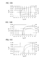
- FIG. 15A shows initial characteristics of a transistor in Sample A.
- FIG. 15B shows initial characteristics of a transistor in Sample B.
- FIG. 15C shows initial characteristics of a transistor in Sample C.
- the field-effect mobility of the transistor in Sample A was 18.8 cm 2 /Vsec.
- the field-effect mobility of the transistor in Sample B was 32.2 cm 2 /Vsec.
- the field-effect mobility of the transistor in Sample C was 34.5 cm 2 /Vsec.
- the crystalline portion is not aligned. Therefore, the sample whose substrate has been heated during deposition, has a novel crystal structure.
- FIGS. 15A to 15C leads to understanding that heat treatment performed on the substrate during or after deposition can remove an hydrogen element serving as a donor, so that the threshold voltage of the n-channel transistor can be shifted in the positive direction.
- the threshold voltage of Sample B in which heating was performed on the substrate during deposition is shifted in the positive direction more than the threshold voltage of Sample A in which heating was not performed on the substrate during deposition.
- the threshold voltage can be shifted more in the positive direction by further increasing of the temperature of heat treatment.
- the gate BT stress test was performed on Sample B (without heat treatment after deposition) and Sample C (with heat treatment after deposition).
- V g ⁇ I d characteristics gate voltage-drain current characteristics of the transistors were measured at a substrate temperature of 25° C. and drain voltage (V d ) of 10 V to measure characteristics of the transistors before heat treatment and high positive voltage application.
- the substrate temperature was set to 150° C. and V d was set to 0.1 V.
- V g gate voltage
- V g was set to 0 V.
- V g ⁇ I d characteristics of the transistors were measured at a substrate temperature of 25° C. and V d of 10 V to measure characteristics of the transistors after heat treatment and high positive voltage application.
- V g ⁇ I d characteristics of the transistors were measured at a substrate temperature of 25° C. and V d of 10 V to measure characteristics of the transistors before heat treatment and high negative voltage application.
- the substrate temperature was set to 150° C. and V d was set to 0.1 V.
- V g was set to 0 V.
- V g ⁇ I d characteristics of the transistors were measured at a substrate temperature of 25° C. and V d of 10 V to measure characteristics of the transistors after heat treatment and high negative voltage application.
- FIG. 16A shows a result of the positive BT test of Sample B and FIG. 16B shows a result of the negative BT test of Sample B.
- FIG. 17A shows a result of the positive BT test of Sample C and FIG. 17B shows a result of the negative BT test of Sample C.
- the positive BT test and the negative BT test are tests used to determine the deterioration level of a transistor, with reference to FIG. 16A and FIG. 17A , it is found that the threshold voltage can be shifted in the positive direction by performing at least the positive BT test.
- FIG. 16A shows that a transistor becomes a normally-off transistor by being subjected to the positive BT test.
- the shift of the threshold voltage in the positive direction can be increased and a normally-off transistor can be formed by performing the positive BT test in addition to the heat treatment at the time of manufacturing the transistor.
- FIG. 18 shows a relation between the off-state current of a transistor in Sample A and the inverse of substrate temperature (absolute temperature) at measurement.
- the abscissa represents a value (1000/T) obtained by multiplying an inverse of substrate temperature at measurement by 1000.
- FIG. 18 illustrates the amount of current in the case where the channel width is 1 ⁇ m.
- the off-state current was lower than or equal to 1 ⁇ 10 ⁇ 19 A when the substrate temperature was 125° C. (1000/T is about 2.51).
- the off-state current was lower than or equal to 1 ⁇ 10 ⁇ 20 A when the substrate temperature was 85° C. (1000/T is about 2.79).
- the off-state current is extremely low compared to a transistor including a silicon semiconductor.
Landscapes
- Engineering & Computer Science (AREA)
- Manufacturing & Machinery (AREA)
- Semiconductor Memories (AREA)
- Dram (AREA)
Abstract
Description
- [Non-Patent Document] K. Kim, “Technology for sub-50 nm DRAM and NAND flash manufacturing”, Technical Digest of International Electron Devices Meeting, pp. 333-336, 2005.
Claims (29)
Priority Applications (1)
Application Number | Priority Date | Filing Date | Title |
---|---|---|---|
US14/227,408 US9196616B2 (en) | 2011-03-31 | 2014-03-27 | Memory device |
Applications Claiming Priority (4)
Application Number | Priority Date | Filing Date | Title |
---|---|---|---|
JP2011078937 | 2011-03-31 | ||
JP2011-078937 | 2011-03-31 | ||
JP2011-108885 | 2011-05-14 | ||
JP2011108885 | 2011-05-14 |
Related Child Applications (1)
Application Number | Title | Priority Date | Filing Date |
---|---|---|---|
US14/227,408 Continuation US9196616B2 (en) | 2011-03-31 | 2014-03-27 | Memory device |
Publications (2)
Publication Number | Publication Date |
---|---|
US20120248434A1 US20120248434A1 (en) | 2012-10-04 |
US8686486B2 true US8686486B2 (en) | 2014-04-01 |
Family
ID=46926030
Family Applications (2)
Application Number | Title | Priority Date | Filing Date |
---|---|---|---|
US13/425,674 Expired - Fee Related US8686486B2 (en) | 2011-03-31 | 2012-03-21 | Memory device |
US14/227,408 Active US9196616B2 (en) | 2011-03-31 | 2014-03-27 | Memory device |
Family Applications After (1)
Application Number | Title | Priority Date | Filing Date |
---|---|---|---|
US14/227,408 Active US9196616B2 (en) | 2011-03-31 | 2014-03-27 | Memory device |
Country Status (3)
Country | Link |
---|---|
US (2) | US8686486B2 (en) |
JP (2) | JP6005378B2 (en) |
KR (1) | KR101999400B1 (en) |
Cited By (7)
Publication number | Priority date | Publication date | Assignee | Title |
---|---|---|---|---|
US9478276B2 (en) | 2014-04-10 | 2016-10-25 | Semiconductor Energy Laboratory Co., Ltd. | Memory device and semiconductor device |
US9607991B2 (en) | 2013-09-05 | 2017-03-28 | Semiconductor Energy Laboratory Co., Ltd. | Semiconductor device |
US9741400B2 (en) | 2015-11-05 | 2017-08-22 | Semiconductor Energy Laboratory Co., Ltd. | Semiconductor device, memory device, electronic device, and method for operating the semiconductor device |
US9947801B2 (en) | 2014-03-28 | 2018-04-17 | Semiconductor Energy Laboratory Co., Ltd. | Transistor and semiconductor device |
US10050087B1 (en) | 2017-03-16 | 2018-08-14 | Toshiba Memory Corporation | Semiconductor memory device |
US10304523B2 (en) | 2014-05-09 | 2019-05-28 | Semiconductor Energy Laboratory Co., Ltd. | Semiconductor device comprising memory devices each comprising sense amplifier and memory cell |
US11101300B2 (en) | 2017-07-26 | 2021-08-24 | Semiconductor Energy Laboratory Co., Ltd. | Semiconductor device and manufacturing method of semiconductor device |
Families Citing this family (7)
Publication number | Priority date | Publication date | Assignee | Title |
---|---|---|---|---|
US8686486B2 (en) * | 2011-03-31 | 2014-04-01 | Semiconductor Energy Laboratory Co., Ltd. | Memory device |
WO2015117222A1 (en) * | 2014-02-05 | 2015-08-13 | Conversant Intellectual Property Management Inc. | A dram memory device with manufacturable capacitor |
US10854612B2 (en) | 2018-03-21 | 2020-12-01 | Samsung Electronics Co., Ltd. | Semiconductor device including active region with variable atomic concentration of oxide semiconductor material and method of forming the same |
CN112490192B (en) * | 2019-09-12 | 2023-03-17 | 夏泰鑫半导体(青岛)有限公司 | Dynamic random access memory and preparation method thereof |
US11335552B2 (en) * | 2020-04-17 | 2022-05-17 | Taiwan Semiconductor Manufacturing Co., Ltd. | Structure and formation method of semiconductor device with oxide semiconductor channel |
KR20230133149A (en) * | 2022-03-10 | 2023-09-19 | 삼성전자주식회사 | Semiconductor memory device |
JP7349045B1 (en) | 2023-07-05 | 2023-09-21 | 正美 柏田 | Retrofit roll cutter |
Citations (138)
Publication number | Priority date | Publication date | Assignee | Title |
---|---|---|---|---|
US4735821A (en) | 1985-09-21 | 1988-04-05 | Semiconductor Energy Laboratory Co., Ltd. | Method for depositing material on depressions |
US5302843A (en) | 1990-07-26 | 1994-04-12 | Semiconductor Energy Laboratory Co., Ltd. | Improved vertical channel transistor |
US5414289A (en) | 1992-03-02 | 1995-05-09 | Motorola, Inc. | Dynamic memory device having a vertical transistor |
US5414288A (en) | 1992-11-19 | 1995-05-09 | Motorola, Inc. | Vertical transistor having an underlying gate electrode contact |
US5462767A (en) | 1985-09-21 | 1995-10-31 | Semiconductor Energy Laboratory Co., Ltd. | CVD of conformal coatings over a depression using alkylmetal precursors |
US5731856A (en) | 1995-12-30 | 1998-03-24 | Samsung Electronics Co., Ltd. | Methods for forming liquid crystal displays including thin film transistors and gate pads having a particular structure |
US5744864A (en) | 1995-08-03 | 1998-04-28 | U.S. Philips Corporation | Semiconductor device having a transparent switching element |
US6018176A (en) | 1995-05-26 | 2000-01-25 | Samsung Electronics Co., Ltd. | Vertical transistor and memory cell |
JP2000044236A (en) | 1998-07-24 | 2000-02-15 | Hoya Corp | Article having transparent conductive oxide thin film and method for producing the same |
JP2000150900A (en) | 1998-11-17 | 2000-05-30 | Japan Science & Technology Corp | Transistor and semiconductor device |
US6294274B1 (en) | 1998-11-16 | 2001-09-25 | Tdk Corporation | Oxide thin film |
US20010025973A1 (en) * | 2000-01-25 | 2001-10-04 | Satoru Yamada | Semiconductor integrated circuit device and process for manufacturing the same |
US20010046027A1 (en) | 1999-09-03 | 2001-11-29 | Ya-Hsiang Tai | Liquid crystal display having stripe-shaped common electrodes formed above plate-shaped pixel electrodes |
US20020030214A1 (en) * | 2000-09-11 | 2002-03-14 | Fumio Horiguchi | Semiconductor device and method for manufacturing the same |
JP2002076356A (en) | 2000-09-01 | 2002-03-15 | Japan Science & Technology Corp | Semiconductor device |
US6365452B1 (en) | 1998-03-19 | 2002-04-02 | Lsi Logic Corporation | DRAM cell having a vertical transistor and a capacitor formed on the sidewalls of a trench isolation |
US20020056838A1 (en) | 2000-11-15 | 2002-05-16 | Matsushita Electric Industrial Co., Ltd. | Thin film transistor array, method of producing the same, and display panel using the same |
US20020132454A1 (en) | 2001-03-19 | 2002-09-19 | Fuji Xerox Co., Ltd. | Method of forming crystalline semiconductor thin film on base substrate, lamination formed with crystalline semiconductor thin film and color filter |
US6459112B1 (en) * | 1999-01-22 | 2002-10-01 | Fujitsu Limited | Semiconductor device and process for fabricating the same |
JP2002289859A (en) | 2001-03-23 | 2002-10-04 | Minolta Co Ltd | Thin film transistor |
US20020173096A1 (en) * | 2001-05-21 | 2002-11-21 | Mitsubishi Denki Kabushiki Kaisha | Semiconductor integrated circuit and method of manufacturing same |
JP2003086808A (en) | 2001-09-10 | 2003-03-20 | Masashi Kawasaki | Thin film transistor and matrix display device |
JP2003086000A (en) | 2001-09-10 | 2003-03-20 | Sharp Corp | Semiconductor memory and its test method |
US6566702B1 (en) * | 1997-12-19 | 2003-05-20 | Micron Technology, Inc. | Spacer patterned, high dielectric constant capacitor |
JP2003152086A (en) | 2001-11-15 | 2003-05-23 | Semiconductor Energy Lab Co Ltd | Semiconductor device |
US6580175B1 (en) * | 1999-11-15 | 2003-06-17 | Samsung Electronics Co., Ltd. | Semiconductor layout structure for a conductive layer and contact hole |
US6621110B1 (en) * | 1999-06-14 | 2003-09-16 | Hitachi, Ltd. | Semiconductor intergrated circuit device and a method of manufacture thereof |
US6630705B2 (en) * | 2000-08-10 | 2003-10-07 | Mitsubishi Denki Kabushiki Kaisha | Semiconductor device with capacitor electrodes |
US20030189401A1 (en) | 2002-03-26 | 2003-10-09 | International Manufacturing And Engineering Services Co., Ltd. | Organic electroluminescent device |
US20030218222A1 (en) | 2002-05-21 | 2003-11-27 | The State Of Oregon Acting And Through The Oregon State Board Of Higher Education On Behalf Of | Transistor structures and methods for making the same |
US20040038446A1 (en) | 2002-03-15 | 2004-02-26 | Sanyo Electric Co., Ltd.- | Method for forming ZnO film, method for forming ZnO semiconductor layer, method for fabricating semiconductor device, and semiconductor device |
US6700152B2 (en) * | 1995-10-27 | 2004-03-02 | Hitachi, Ltd. | Dynamic random access memory including a logic circuit and an improved storage capacitor arrangement |
JP2004103957A (en) | 2002-09-11 | 2004-04-02 | Japan Science & Technology Corp | Transparent thin film field effect transistor using homologous thin film as active layer |
US6734484B2 (en) | 2002-08-26 | 2004-05-11 | Intellignet Sources Development Corp. | Vertical transistor DRAM structure and its manufacturing methods |
US20040127038A1 (en) | 2002-10-11 | 2004-07-01 | Carcia Peter Francis | Transparent oxide semiconductor thin film transistors |
US20040135190A1 (en) * | 2002-12-10 | 2004-07-15 | Reidar Lindstedt | Semiconductor memory having an arrangement of memory cells |
JP2004273732A (en) | 2003-03-07 | 2004-09-30 | Sharp Corp | Active matrix substrate and its producing process |
JP2004273614A (en) | 2003-03-06 | 2004-09-30 | Sharp Corp | Semiconductor device and its fabricating process |
WO2004114391A1 (en) | 2003-06-20 | 2004-12-29 | Sharp Kabushiki Kaisha | Semiconductor device, its manufacturing method, and electronic device |
US20050017302A1 (en) | 2003-07-25 | 2005-01-27 | Randy Hoffman | Transistor including a deposited channel region having a doped portion |
US20050040452A1 (en) * | 1997-06-30 | 2005-02-24 | Hitachi, Ltd. | Method for fabricating semiconductor integrated circuit |
US6878990B2 (en) | 2001-12-31 | 2005-04-12 | Hynix Semiconductor, Inc. | Vertical transistor and method of manufacturing thereof |
US20050199959A1 (en) | 2004-03-12 | 2005-09-15 | Chiang Hai Q. | Semiconductor device |
US20060043377A1 (en) | 2004-03-12 | 2006-03-02 | Hewlett-Packard Development Company, L.P. | Semiconductor device |
US20060091793A1 (en) | 2004-11-02 | 2006-05-04 | 3M Innovative Properties Company | Methods and displays utilizing integrated zinc oxide row and column drivers in conjunction with organic light emitting diodes |
US20060108636A1 (en) | 2004-11-10 | 2006-05-25 | Canon Kabushiki Kaisha | Amorphous oxide and field effect transistor |
US20060110867A1 (en) | 2004-11-10 | 2006-05-25 | Canon Kabushiki Kaisha | Field effect transistor manufacturing method |
US20060108529A1 (en) | 2004-11-10 | 2006-05-25 | Canon Kabushiki Kaisha | Sensor and image pickup device |
US20060113565A1 (en) | 2004-11-10 | 2006-06-01 | Canon Kabushiki Kaisha | Electric elements and circuits utilizing amorphous oxides |
US20060113536A1 (en) | 2004-11-10 | 2006-06-01 | Canon Kabushiki Kaisha | Display |
US20060113549A1 (en) | 2004-11-10 | 2006-06-01 | Canon Kabushiki Kaisha | Light-emitting device |
US20060113539A1 (en) | 2004-11-10 | 2006-06-01 | Canon Kabushiki Kaisha | Field effect transistor |
US7056786B2 (en) * | 2003-09-01 | 2006-06-06 | Samsung Electronics Co., Ltd | Self-aligned buried contact pair and method of forming the same |
US7061014B2 (en) | 2001-11-05 | 2006-06-13 | Japan Science And Technology Agency | Natural-superlattice homologous single crystal thin film, method for preparation thereof, and device using said single crystal thin film |
US20060170111A1 (en) | 2005-01-28 | 2006-08-03 | Semiconductor Energy Laboratory Co., Ltd. | Semiconductor device, electronic device, and method of manufacturing semiconductor device |
US20060169973A1 (en) | 2005-01-28 | 2006-08-03 | Semiconductor Energy Laboratory Co., Ltd. | Semiconductor device, electronic device, and method of manufacturing semiconductor device |
US20060186453A1 (en) * | 2005-02-21 | 2006-08-24 | Samsung Electronics Co., Ltd. | Semiconductor device having a capacitor and a fabrication method thereof |
US20060197092A1 (en) | 2005-03-03 | 2006-09-07 | Randy Hoffman | System and method for forming conductive material on a substrate |
US7105868B2 (en) | 2002-06-24 | 2006-09-12 | Cermet, Inc. | High-electron mobility transistor with zinc oxide |
US20060208977A1 (en) | 2005-03-18 | 2006-09-21 | Semiconductor Energy Laboratory Co., Ltd. | Semiconductor device, and display device, driving method and electronic apparatus thereof |
US20060228974A1 (en) | 2005-03-31 | 2006-10-12 | Theiss Steven D | Methods of making displays |
US20060231882A1 (en) | 2005-03-28 | 2006-10-19 | Il-Doo Kim | Low voltage flexible organic/transparent transistor for selective gas sensing, photodetecting and CMOS device applications |
US20060238135A1 (en) | 2005-04-20 | 2006-10-26 | Semiconductor Energy Laboratory Co., Ltd. | Semiconductor device and display device |
US20060255384A1 (en) * | 2005-05-13 | 2006-11-16 | Peter Baars | Memory device and method of manufacturing the same |
US20060284172A1 (en) | 2005-06-10 | 2006-12-21 | Casio Computer Co., Ltd. | Thin film transistor having oxide semiconductor layer and manufacturing method thereof |
US20060284171A1 (en) | 2005-06-16 | 2006-12-21 | Levy David H | Methods of making thin film transistors comprising zinc-oxide-based semiconductor materials and transistors made thereby |
EP1737044A1 (en) | 2004-03-12 | 2006-12-27 | Japan Science and Technology Agency | Amorphous oxide and thin film transistor |
US20060292777A1 (en) | 2005-06-27 | 2006-12-28 | 3M Innovative Properties Company | Method for making electronic devices using metal oxide nanoparticles |
US20070024187A1 (en) | 2005-07-28 | 2007-02-01 | Shin Hyun S | Organic light emitting display (OLED) and its method of fabrication |
US20070045703A1 (en) * | 2005-08-25 | 2007-03-01 | Hynix Semiconductor Inc. | Semiconductor device and method for fabricating the same |
US20070046191A1 (en) | 2005-08-23 | 2007-03-01 | Canon Kabushiki Kaisha | Organic electroluminescent display device and manufacturing method thereof |
US20070052025A1 (en) | 2005-09-06 | 2007-03-08 | Canon Kabushiki Kaisha | Oxide semiconductor thin film transistor and method of manufacturing the same |
US20070054507A1 (en) | 2005-09-06 | 2007-03-08 | Canon Kabushiki Kaisha | Method of fabricating oxide semiconductor device |
US20070090365A1 (en) | 2005-10-20 | 2007-04-26 | Canon Kabushiki Kaisha | Field-effect transistor including transparent oxide and light-shielding member, and display utilizing the transistor |
US7211825B2 (en) | 2004-06-14 | 2007-05-01 | Yi-Chi Shih | Indium oxide-based thin film transistors and circuits |
US20070108446A1 (en) | 2005-11-15 | 2007-05-17 | Semiconductor Energy Laboratory Co., Ltd. | Semiconductor device and manufacturing method thereof |
US20070146008A1 (en) | 2005-12-22 | 2007-06-28 | Nam-Kyun Tak | Semiconductor circuit comprising vertical transistor |
US20070152217A1 (en) | 2005-12-29 | 2007-07-05 | Chih-Ming Lai | Pixel structure of active matrix organic light-emitting diode and method for fabricating the same |
US20070172591A1 (en) | 2006-01-21 | 2007-07-26 | Samsung Electronics Co., Ltd. | METHOD OF FABRICATING ZnO FILM AND THIN FILM TRANSISTOR ADOPTING THE ZnO FILM |
US20070187760A1 (en) | 2006-02-02 | 2007-08-16 | Kochi Industrial Promotion Center | Thin film transistor including low resistance conductive thin films and manufacturing method thereof |
US20070187678A1 (en) | 2006-02-15 | 2007-08-16 | Kochi Industrial Promotion Center | Semiconductor device including active layer made of zinc oxide with controlled orientations and manufacturing method thereof |
US20070252928A1 (en) | 2006-04-28 | 2007-11-01 | Toppan Printing Co., Ltd. | Structure, transmission type liquid crystal display, reflection type display and manufacturing method thereof |
US7297977B2 (en) | 2004-03-12 | 2007-11-20 | Hewlett-Packard Development Company, L.P. | Semiconductor device |
US20070272922A1 (en) | 2006-04-11 | 2007-11-29 | Samsung Electronics Co. Ltd. | ZnO thin film transistor and method of forming the same |
US20070287296A1 (en) | 2006-06-13 | 2007-12-13 | Canon Kabushiki Kaisha | Dry etching method for oxide semiconductor film |
US20080006877A1 (en) | 2004-09-17 | 2008-01-10 | Peter Mardilovich | Method of Forming a Solution Processed Device |
US7323356B2 (en) | 2002-02-21 | 2008-01-29 | Japan Science And Technology Agency | LnCuO(S,Se,Te)monocrystalline thin film, its manufacturing method, and optical device or electronic device using the monocrystalline thin film |
US20080038929A1 (en) | 2006-08-09 | 2008-02-14 | Canon Kabushiki Kaisha | Method of dry etching oxide semiconductor film |
US20080038882A1 (en) | 2006-08-09 | 2008-02-14 | Kazushige Takechi | Thin-film device and method of fabricating the same |
US20080050595A1 (en) | 2006-01-11 | 2008-02-28 | Murata Manufacturing Co., Ltd. | Transparent conductive film and method for manufacturing the same |
US20080073653A1 (en) | 2006-09-27 | 2008-03-27 | Canon Kabushiki Kaisha | Semiconductor apparatus and method of manufacturing the same |
US20080083950A1 (en) | 2006-10-10 | 2008-04-10 | Alfred I-Tsung Pan | Fused nanocrystal thin film semiconductor and method |
US20080106191A1 (en) | 2006-09-27 | 2008-05-08 | Seiko Epson Corporation | Electronic device, organic electroluminescence device, and organic thin film semiconductor device |
US20080121960A1 (en) * | 2006-11-24 | 2008-05-29 | Elpida Memory, Inc. | Semiconductor device and method of forming the same |
US7382014B2 (en) * | 2005-05-17 | 2008-06-03 | Elpida Memory, Inc. | Semiconductor device with capacitor suppressing leak current |
US20080128689A1 (en) | 2006-11-29 | 2008-06-05 | Je-Hun Lee | Flat panel displays comprising a thin-film transistor having a semiconductive oxide in its channel and methods of fabricating the same for use in flat panel displays |
US20080129195A1 (en) | 2006-12-04 | 2008-06-05 | Toppan Printing Co., Ltd. | Color el display and method for producing the same |
US7385224B2 (en) | 2004-09-02 | 2008-06-10 | Casio Computer Co., Ltd. | Thin film transistor having an etching protection film and manufacturing method thereof |
US20080149913A1 (en) | 2006-12-26 | 2008-06-26 | Hiroyasu Tanaka | Semiconductor memory device and method of manufacturing the same |
US20080166834A1 (en) | 2007-01-05 | 2008-07-10 | Samsung Electronics Co., Ltd. | Thin film etching method |
US7402506B2 (en) | 2005-06-16 | 2008-07-22 | Eastman Kodak Company | Methods of making thin film transistors comprising zinc-oxide-based semiconductor materials and transistors made thereby |
US20080175032A1 (en) | 2007-01-23 | 2008-07-24 | Kabushiki Kaisha Toshiba | Semiconductor memory and method for manufacturing the same |
US20080182358A1 (en) | 2007-01-26 | 2008-07-31 | Cowdery-Corvan Peter J | Process for atomic layer deposition |
US7411209B2 (en) | 2006-09-15 | 2008-08-12 | Canon Kabushiki Kaisha | Field-effect transistor and method for manufacturing the same |
US20080224133A1 (en) | 2007-03-14 | 2008-09-18 | Jin-Seong Park | Thin film transistor and organic light-emitting display device having the thin film transistor |
US20080258140A1 (en) | 2007-04-20 | 2008-10-23 | Samsung Electronics Co., Ltd. | Thin film transistor including selectively crystallized channel layer and method of manufacturing the thin film transistor |
US20080258143A1 (en) | 2007-04-18 | 2008-10-23 | Samsung Electronics Co., Ltd. | Thin film transitor substrate and method of manufacturing the same |
US20080258139A1 (en) | 2007-04-17 | 2008-10-23 | Toppan Printing Co., Ltd. | Structure with transistor |
US20080258141A1 (en) | 2007-04-19 | 2008-10-23 | Samsung Electronics Co., Ltd. | Thin film transistor, method of manufacturing the same, and flat panel display having the same |
US7453087B2 (en) | 2005-09-06 | 2008-11-18 | Canon Kabushiki Kaisha | Thin-film transistor and thin-film diode having amorphous-oxide semiconductor layer |
US20080296568A1 (en) | 2007-05-29 | 2008-12-04 | Samsung Electronics Co., Ltd | Thin film transistors and methods of manufacturing the same |
US7501293B2 (en) | 2002-06-13 | 2009-03-10 | Murata Manufacturing Co., Ltd. | Semiconductor device in which zinc oxide is used as a semiconductor material and method for manufacturing the semiconductor device |
US20090073325A1 (en) | 2005-01-21 | 2009-03-19 | Semiconductor Energy Laboratory Co., Ltd. | Semiconductor device and method for manufacturing the same, and electric device |
US20090114910A1 (en) | 2005-09-06 | 2009-05-07 | Canon Kabushiki Kaisha | Semiconductor device |
US20090134399A1 (en) | 2005-02-18 | 2009-05-28 | Semiconductor Energy Laboratory Co., Ltd. | Semiconductor Device and Method for Manufacturing the Same |
US20090152541A1 (en) | 2005-02-03 | 2009-06-18 | Semiconductor Energy Laboratory Co., Ltd. | Electronic device, semiconductor device and manufacturing method thereof |
US20090152506A1 (en) | 2007-12-17 | 2009-06-18 | Fujifilm Corporation | Process for producing oriented inorganic crystalline film, and semiconductor device using the oriented inorganic crystalline film |
US20100038709A1 (en) | 2008-08-15 | 2010-02-18 | Nanya Technology Corporation | Vertical transistor and array with vertical transistors |
US7674650B2 (en) | 2005-09-29 | 2010-03-09 | Semiconductor Energy Laboratory Co., Ltd. | Semiconductor device and manufacturing method thereof |
US20100065844A1 (en) | 2008-09-18 | 2010-03-18 | Sony Corporation | Thin film transistor and method of manufacturing thin film transistor |
US20100092800A1 (en) | 2008-10-09 | 2010-04-15 | Canon Kabushiki Kaisha | Substrate for growing wurtzite type crystal and method for manufacturing the same and semiconductor device |
US20100109002A1 (en) | 2007-04-25 | 2010-05-06 | Canon Kabushiki Kaisha | Oxynitride semiconductor |
US7781285B2 (en) | 2005-10-10 | 2010-08-24 | Samsung Electronics Co., Ltd. | Semiconductor device having vertical transistor and method of fabricating the same |
US7936004B2 (en) | 2006-03-27 | 2011-05-03 | Kabushiki Kaisha Toshiba | Nonvolatile semiconductor memory device and manufacturing method thereof |
US20110101356A1 (en) | 2009-10-30 | 2011-05-05 | Semiconductor Energy Laboratory Co., Ltd. | Transistor |
US20110122670A1 (en) | 2009-11-20 | 2011-05-26 | Semiconductor Energy Laboratory Co., Ltd. | Semiconductor device |
US20110121284A1 (en) | 2009-11-20 | 2011-05-26 | Semiconductor Energy Laboratory Co., Ltd. | Transistor |
US20110127526A1 (en) | 2009-11-27 | 2011-06-02 | Semiconductor Energy Laboratory Co., Ltd. | Non-linear element, display device including non-linear element, and electronic device including display device |
US20110205777A1 (en) | 2007-08-29 | 2011-08-25 | Elpida Memory, Inc. | Semiconductor memory device having vertical transistors |
US20110260169A1 (en) * | 2006-09-29 | 2011-10-27 | Semiconductor Energy Laboratory Co., Ltd. | Display device and electronic device |
US20120033483A1 (en) | 2010-08-06 | 2012-02-09 | Semiconductor Energy Laboratory Co., Ltd. | Semiconductor device and driving method of semiconductor device |
US20120049184A1 (en) * | 2006-09-29 | 2012-03-01 | Semiconductor Energy Laboratory Co., Ltd. | Display device |
US20120187417A1 (en) * | 2011-01-26 | 2012-07-26 | Semiconductor Energy Laboratory Co., Ltd. | Semiconductor device |
US20120187475A1 (en) * | 2011-01-26 | 2012-07-26 | Semiconductor Energy Laboratory Co., Ltd. | Semiconductor device and manufacturing method thereof |
US20120193696A1 (en) * | 2011-01-28 | 2012-08-02 | Elpida Memory, Inc. | Semiconductor device and method for manufacturing the same |
US20120199842A1 (en) * | 2011-02-08 | 2012-08-09 | Semiconductor Energy Laboratory Co., Ltd. | Semiconductor memory device and method for manufacturing the same |
US20120228688A1 (en) * | 2011-03-10 | 2012-09-13 | Semiconductor Energy Laboratory Co., Ltd. | Memory device and method for manufacturing the same |
US20120248434A1 (en) * | 2011-03-31 | 2012-10-04 | Semiconductor Energy Laboratory Co., Ltd. | Memory device |
Family Cites Families (28)
Publication number | Priority date | Publication date | Assignee | Title |
---|---|---|---|---|
JPS60198861A (en) | 1984-03-23 | 1985-10-08 | Fujitsu Ltd | Thin film transistor |
JPH0244256B2 (en) | 1987-01-28 | 1990-10-03 | Kagaku Gijutsucho Mukizaishitsu Kenkyushocho | INGAZN2O5DESHIMESARERUROTSUHOSHOKEINOSOJOKOZOOJUSURUKAGOBUTSUOYOBISONOSEIZOHO |
JPH0244258B2 (en) | 1987-02-24 | 1990-10-03 | Kagaku Gijutsucho Mukizaishitsu Kenkyushocho | INGAZN3O6DESHIMESARERUROTSUHOSHOKEINOSOJOKOZOOJUSURUKAGOBUTSUOYOBISONOSEIZOHO |
JPS63210023A (en) | 1987-02-24 | 1988-08-31 | Natl Inst For Res In Inorg Mater | Compound having a hexagonal layered structure represented by InGaZn↓4O↓7 and its manufacturing method |
JPH0244260B2 (en) | 1987-02-24 | 1990-10-03 | Kagaku Gijutsucho Mukizaishitsu Kenkyushocho | INGAZN5O8DESHIMESARERUROTSUHOSHOKEINOSOJOKOZOOJUSURUKAGOBUTSUOYOBISONOSEIZOHO |
JPH0244262B2 (en) | 1987-02-27 | 1990-10-03 | Kagaku Gijutsucho Mukizaishitsu Kenkyushocho | INGAZN6O9DESHIMESARERUROTSUHOSHOKEINOSOJOKOZOOJUSURUKAGOBUTSUOYOBISONOSEIZOHO |
JPH0244263B2 (en) | 1987-04-22 | 1990-10-03 | Kagaku Gijutsucho Mukizaishitsu Kenkyushocho | INGAZN7O10DESHIMESARERUROTSUHOSHOKEINOSOJOKOZOOJUSURUKAGOBUTSUOYOBISONOSEIZOHO |
JPH02198170A (en) * | 1989-01-27 | 1990-08-06 | Hitachi Ltd | Semiconductor integrated circuit device and manufacture thereof |
JP3128829B2 (en) * | 1990-12-26 | 2001-01-29 | ソニー株式会社 | Semiconductor memory device |
JP3003188B2 (en) * | 1990-09-10 | 2000-01-24 | ソニー株式会社 | Semiconductor memory and manufacturing method thereof |
JP3158462B2 (en) * | 1991-03-11 | 2001-04-23 | 松下電器産業株式会社 | Semiconductor memory device and method of manufacturing the same |
TW215967B (en) * | 1992-01-17 | 1993-11-11 | Seiko Electron Co Ltd | MOS Poly-Si thin film transistor with a flattened channel interface and method of producing same |
JPH05251705A (en) | 1992-03-04 | 1993-09-28 | Fuji Xerox Co Ltd | Thin-film transistor |
JPH06334146A (en) * | 1993-05-26 | 1994-12-02 | Toshiba Corp | Semiconductor device |
JP3745392B2 (en) * | 1994-05-26 | 2006-02-15 | 株式会社ルネサステクノロジ | Semiconductor device |
JP3479375B2 (en) | 1995-03-27 | 2003-12-15 | 科学技術振興事業団 | Metal oxide semiconductor device in which a pn junction is formed with a thin film transistor made of a metal oxide semiconductor such as cuprous oxide, and methods for manufacturing the same |
TW335503B (en) * | 1996-02-23 | 1998-07-01 | Semiconductor Energy Lab Kk | Semiconductor thin film and manufacturing method and semiconductor device and its manufacturing method |
US6576945B2 (en) * | 2001-02-05 | 2003-06-10 | International Business Machines Corporation | Structure and method for a compact trench-capacitor DRAM cell with body contact |
US6559491B2 (en) * | 2001-02-09 | 2003-05-06 | Micron Technology, Inc. | Folded bit line DRAM with ultra thin body transistors |
JP2002319682A (en) * | 2002-01-04 | 2002-10-31 | Japan Science & Technology Corp | Transistor and semiconductor device |
KR20040093300A (en) * | 2003-04-29 | 2004-11-05 | 주식회사 하이닉스반도체 | Fabricating method of capacitor in semiconductor memory device |
DE10339529A1 (en) * | 2003-08-21 | 2005-03-24 | Hahn-Meitner-Institut Berlin Gmbh | Vertical nano-transistor, method for its manufacture and memory arrangement |
JP4568286B2 (en) * | 2004-10-04 | 2010-10-27 | パナソニック株式会社 | Vertical field effect transistor and manufacturing method thereof |
JP5202094B2 (en) * | 2008-05-12 | 2013-06-05 | キヤノン株式会社 | Semiconductor device |
KR20100038986A (en) * | 2008-10-07 | 2010-04-15 | 삼성전자주식회사 | Multi-layered memory apparatus comprising oxide thin film transistor |
KR101201891B1 (en) * | 2009-03-26 | 2012-11-16 | 한국전자통신연구원 | The transparent non-volatile memory thin film transistor and the manufacturing method thereof |
JP2011003598A (en) * | 2009-06-16 | 2011-01-06 | Elpida Memory Inc | Method of manufacturing semiconductor device |
JP2011138934A (en) * | 2009-12-28 | 2011-07-14 | Sony Corp | Thin film transistor, display device, and electronic equipment |
-
2012
- 2012-03-21 US US13/425,674 patent/US8686486B2/en not_active Expired - Fee Related
- 2012-03-28 JP JP2012073596A patent/JP6005378B2/en active Active
- 2012-03-30 KR KR1020120033208A patent/KR101999400B1/en active IP Right Grant
-
2014
- 2014-03-27 US US14/227,408 patent/US9196616B2/en active Active
-
2016
- 2016-09-07 JP JP2016174159A patent/JP6224794B2/en not_active Expired - Fee Related
Patent Citations (168)
Publication number | Priority date | Publication date | Assignee | Title |
---|---|---|---|---|
US5462767A (en) | 1985-09-21 | 1995-10-31 | Semiconductor Energy Laboratory Co., Ltd. | CVD of conformal coatings over a depression using alkylmetal precursors |
US4861622A (en) | 1985-09-21 | 1989-08-29 | Semiconductor Energy Laboratory Co., Ltd. | Method for forming a film coat on the inside of a depression |
US5084130A (en) | 1985-09-21 | 1992-01-28 | Semiconductor Energy Laboratory Co., Ltd. | Method for depositing material on depressions |
US4735821A (en) | 1985-09-21 | 1988-04-05 | Semiconductor Energy Laboratory Co., Ltd. | Method for depositing material on depressions |
US5302843A (en) | 1990-07-26 | 1994-04-12 | Semiconductor Energy Laboratory Co., Ltd. | Improved vertical channel transistor |
US5403763A (en) | 1990-07-26 | 1995-04-04 | Semiconductor Energy Laboratory Co., Ltd. | Method of manufacturing a vertical channel FET |
US5414289A (en) | 1992-03-02 | 1995-05-09 | Motorola, Inc. | Dynamic memory device having a vertical transistor |
US5414288A (en) | 1992-11-19 | 1995-05-09 | Motorola, Inc. | Vertical transistor having an underlying gate electrode contact |
US6018176A (en) | 1995-05-26 | 2000-01-25 | Samsung Electronics Co., Ltd. | Vertical transistor and memory cell |
US5744864A (en) | 1995-08-03 | 1998-04-28 | U.S. Philips Corporation | Semiconductor device having a transparent switching element |
US6700152B2 (en) * | 1995-10-27 | 2004-03-02 | Hitachi, Ltd. | Dynamic random access memory including a logic circuit and an improved storage capacitor arrangement |
US5731856A (en) | 1995-12-30 | 1998-03-24 | Samsung Electronics Co., Ltd. | Methods for forming liquid crystal displays including thin film transistors and gate pads having a particular structure |
US20050040452A1 (en) * | 1997-06-30 | 2005-02-24 | Hitachi, Ltd. | Method for fabricating semiconductor integrated circuit |
US6815754B2 (en) * | 1997-12-19 | 2004-11-09 | Micron Technology, Inc. | Spacer patterned, high dielectric constant capacitor |
US6566702B1 (en) * | 1997-12-19 | 2003-05-20 | Micron Technology, Inc. | Spacer patterned, high dielectric constant capacitor |
US6365452B1 (en) | 1998-03-19 | 2002-04-02 | Lsi Logic Corporation | DRAM cell having a vertical transistor and a capacitor formed on the sidewalls of a trench isolation |
JP2000044236A (en) | 1998-07-24 | 2000-02-15 | Hoya Corp | Article having transparent conductive oxide thin film and method for producing the same |
US6294274B1 (en) | 1998-11-16 | 2001-09-25 | Tdk Corporation | Oxide thin film |
US7064346B2 (en) | 1998-11-17 | 2006-06-20 | Japan Science And Technology Agency | Transistor and semiconductor device |
JP2000150900A (en) | 1998-11-17 | 2000-05-30 | Japan Science & Technology Corp | Transistor and semiconductor device |
US6727522B1 (en) | 1998-11-17 | 2004-04-27 | Japan Science And Technology Corporation | Transistor and semiconductor device |
US6459112B1 (en) * | 1999-01-22 | 2002-10-01 | Fujitsu Limited | Semiconductor device and process for fabricating the same |
US6809364B2 (en) * | 1999-06-14 | 2004-10-26 | Hitachi, Ltd. | Semiconductor integrated circuit device and a method of manufacture thereof |
US6621110B1 (en) * | 1999-06-14 | 2003-09-16 | Hitachi, Ltd. | Semiconductor intergrated circuit device and a method of manufacture thereof |
US20010046027A1 (en) | 1999-09-03 | 2001-11-29 | Ya-Hsiang Tai | Liquid crystal display having stripe-shaped common electrodes formed above plate-shaped pixel electrodes |
US6580175B1 (en) * | 1999-11-15 | 2003-06-17 | Samsung Electronics Co., Ltd. | Semiconductor layout structure for a conductive layer and contact hole |
US20010025973A1 (en) * | 2000-01-25 | 2001-10-04 | Satoru Yamada | Semiconductor integrated circuit device and process for manufacturing the same |
US6630705B2 (en) * | 2000-08-10 | 2003-10-07 | Mitsubishi Denki Kabushiki Kaisha | Semiconductor device with capacitor electrodes |
JP2002076356A (en) | 2000-09-01 | 2002-03-15 | Japan Science & Technology Corp | Semiconductor device |
JP2002094027A (en) | 2000-09-11 | 2002-03-29 | Toshiba Corp | Semiconductor memory device and its manufacturing method |
US7042040B2 (en) | 2000-09-11 | 2006-05-09 | Kabushiki Kaisha Toshiba | Semiconductor device and method for manufacturing the same |
US20020030214A1 (en) * | 2000-09-11 | 2002-03-14 | Fumio Horiguchi | Semiconductor device and method for manufacturing the same |
US20020056838A1 (en) | 2000-11-15 | 2002-05-16 | Matsushita Electric Industrial Co., Ltd. | Thin film transistor array, method of producing the same, and display panel using the same |
US20020132454A1 (en) | 2001-03-19 | 2002-09-19 | Fuji Xerox Co., Ltd. | Method of forming crystalline semiconductor thin film on base substrate, lamination formed with crystalline semiconductor thin film and color filter |
JP2002289859A (en) | 2001-03-23 | 2002-10-04 | Minolta Co Ltd | Thin film transistor |
US20020173096A1 (en) * | 2001-05-21 | 2002-11-21 | Mitsubishi Denki Kabushiki Kaisha | Semiconductor integrated circuit and method of manufacturing same |
JP2003086000A (en) | 2001-09-10 | 2003-03-20 | Sharp Corp | Semiconductor memory and its test method |
JP2003086808A (en) | 2001-09-10 | 2003-03-20 | Masashi Kawasaki | Thin film transistor and matrix display device |
US6563174B2 (en) | 2001-09-10 | 2003-05-13 | Sharp Kabushiki Kaisha | Thin film transistor and matrix display device |
US7061014B2 (en) | 2001-11-05 | 2006-06-13 | Japan Science And Technology Agency | Natural-superlattice homologous single crystal thin film, method for preparation thereof, and device using said single crystal thin film |
JP2003152086A (en) | 2001-11-15 | 2003-05-23 | Semiconductor Energy Lab Co Ltd | Semiconductor device |
US6878990B2 (en) | 2001-12-31 | 2005-04-12 | Hynix Semiconductor, Inc. | Vertical transistor and method of manufacturing thereof |
US7323356B2 (en) | 2002-02-21 | 2008-01-29 | Japan Science And Technology Agency | LnCuO(S,Se,Te)monocrystalline thin film, its manufacturing method, and optical device or electronic device using the monocrystalline thin film |
US20040038446A1 (en) | 2002-03-15 | 2004-02-26 | Sanyo Electric Co., Ltd.- | Method for forming ZnO film, method for forming ZnO semiconductor layer, method for fabricating semiconductor device, and semiconductor device |
US7049190B2 (en) | 2002-03-15 | 2006-05-23 | Sanyo Electric Co., Ltd. | Method for forming ZnO film, method for forming ZnO semiconductor layer, method for fabricating semiconductor device, and semiconductor device |
US20030189401A1 (en) | 2002-03-26 | 2003-10-09 | International Manufacturing And Engineering Services Co., Ltd. | Organic electroluminescent device |
US20030218222A1 (en) | 2002-05-21 | 2003-11-27 | The State Of Oregon Acting And Through The Oregon State Board Of Higher Education On Behalf Of | Transistor structures and methods for making the same |
US7501293B2 (en) | 2002-06-13 | 2009-03-10 | Murata Manufacturing Co., Ltd. | Semiconductor device in which zinc oxide is used as a semiconductor material and method for manufacturing the semiconductor device |
US7105868B2 (en) | 2002-06-24 | 2006-09-12 | Cermet, Inc. | High-electron mobility transistor with zinc oxide |
US6734484B2 (en) | 2002-08-26 | 2004-05-11 | Intellignet Sources Development Corp. | Vertical transistor DRAM structure and its manufacturing methods |
JP2004103957A (en) | 2002-09-11 | 2004-04-02 | Japan Science & Technology Corp | Transparent thin film field effect transistor using homologous thin film as active layer |
US20040127038A1 (en) | 2002-10-11 | 2004-07-01 | Carcia Peter Francis | Transparent oxide semiconductor thin film transistors |
US20060035452A1 (en) | 2002-10-11 | 2006-02-16 | Carcia Peter F | Transparent oxide semiconductor thin film transistor |
US20040135190A1 (en) * | 2002-12-10 | 2004-07-15 | Reidar Lindstedt | Semiconductor memory having an arrangement of memory cells |
JP2004273614A (en) | 2003-03-06 | 2004-09-30 | Sharp Corp | Semiconductor device and its fabricating process |
JP2004273732A (en) | 2003-03-07 | 2004-09-30 | Sharp Corp | Active matrix substrate and its producing process |
US20060244107A1 (en) | 2003-06-20 | 2006-11-02 | Toshinori Sugihara | Semiconductor device, manufacturing method, and electronic device |
WO2004114391A1 (en) | 2003-06-20 | 2004-12-29 | Sharp Kabushiki Kaisha | Semiconductor device, its manufacturing method, and electronic device |
US20050017302A1 (en) | 2003-07-25 | 2005-01-27 | Randy Hoffman | Transistor including a deposited channel region having a doped portion |
US7388243B2 (en) * | 2003-09-01 | 2008-06-17 | Samsung Electronics Co., Ltd. | Self-Aligned buried contact pair |
US20060205147A1 (en) * | 2003-09-01 | 2006-09-14 | Samsung Electronics Co., Ltd. | Self-aligned buried contact pair |
US7056786B2 (en) * | 2003-09-01 | 2006-06-06 | Samsung Electronics Co., Ltd | Self-aligned buried contact pair and method of forming the same |
US20060043377A1 (en) | 2004-03-12 | 2006-03-02 | Hewlett-Packard Development Company, L.P. | Semiconductor device |
US20090278122A1 (en) | 2004-03-12 | 2009-11-12 | Japan Science And Technology Agency | Amorphous oxide and thin film transistor |
US20050199959A1 (en) | 2004-03-12 | 2005-09-15 | Chiang Hai Q. | Semiconductor device |
EP1737044A1 (en) | 2004-03-12 | 2006-12-27 | Japan Science and Technology Agency | Amorphous oxide and thin film transistor |
US7297977B2 (en) | 2004-03-12 | 2007-11-20 | Hewlett-Packard Development Company, L.P. | Semiconductor device |
US20080254569A1 (en) | 2004-03-12 | 2008-10-16 | Hoffman Randy L | Semiconductor Device |
US7282782B2 (en) | 2004-03-12 | 2007-10-16 | Hewlett-Packard Development Company, L.P. | Combined binary oxide semiconductor device |
US20070194379A1 (en) | 2004-03-12 | 2007-08-23 | Japan Science And Technology Agency | Amorphous Oxide And Thin Film Transistor |
US7462862B2 (en) | 2004-03-12 | 2008-12-09 | Hewlett-Packard Development Company, L.P. | Transistor using an isovalent semiconductor oxide as the active channel layer |
EP2226847A2 (en) | 2004-03-12 | 2010-09-08 | Japan Science And Technology Agency | Amorphous oxide and thin film transistor |
US20090280600A1 (en) | 2004-03-12 | 2009-11-12 | Japan Science And Technology Agency | Amorphous oxide and thin film transistor |
US7211825B2 (en) | 2004-06-14 | 2007-05-01 | Yi-Chi Shih | Indium oxide-based thin film transistors and circuits |
US7385224B2 (en) | 2004-09-02 | 2008-06-10 | Casio Computer Co., Ltd. | Thin film transistor having an etching protection film and manufacturing method thereof |
US20080006877A1 (en) | 2004-09-17 | 2008-01-10 | Peter Mardilovich | Method of Forming a Solution Processed Device |
US20060091793A1 (en) | 2004-11-02 | 2006-05-04 | 3M Innovative Properties Company | Methods and displays utilizing integrated zinc oxide row and column drivers in conjunction with organic light emitting diodes |
US20060108636A1 (en) | 2004-11-10 | 2006-05-25 | Canon Kabushiki Kaisha | Amorphous oxide and field effect transistor |
US20060113565A1 (en) | 2004-11-10 | 2006-06-01 | Canon Kabushiki Kaisha | Electric elements and circuits utilizing amorphous oxides |
US20060113549A1 (en) | 2004-11-10 | 2006-06-01 | Canon Kabushiki Kaisha | Light-emitting device |
US20060113536A1 (en) | 2004-11-10 | 2006-06-01 | Canon Kabushiki Kaisha | Display |
US20060108529A1 (en) | 2004-11-10 | 2006-05-25 | Canon Kabushiki Kaisha | Sensor and image pickup device |
US20060113539A1 (en) | 2004-11-10 | 2006-06-01 | Canon Kabushiki Kaisha | Field effect transistor |
US7453065B2 (en) | 2004-11-10 | 2008-11-18 | Canon Kabushiki Kaisha | Sensor and image pickup device |
US20060110867A1 (en) | 2004-11-10 | 2006-05-25 | Canon Kabushiki Kaisha | Field effect transistor manufacturing method |
US20090073325A1 (en) | 2005-01-21 | 2009-03-19 | Semiconductor Energy Laboratory Co., Ltd. | Semiconductor device and method for manufacturing the same, and electric device |
US20060170111A1 (en) | 2005-01-28 | 2006-08-03 | Semiconductor Energy Laboratory Co., Ltd. | Semiconductor device, electronic device, and method of manufacturing semiconductor device |
US20060169973A1 (en) | 2005-01-28 | 2006-08-03 | Semiconductor Energy Laboratory Co., Ltd. | Semiconductor device, electronic device, and method of manufacturing semiconductor device |
US20090152541A1 (en) | 2005-02-03 | 2009-06-18 | Semiconductor Energy Laboratory Co., Ltd. | Electronic device, semiconductor device and manufacturing method thereof |
US20090134399A1 (en) | 2005-02-18 | 2009-05-28 | Semiconductor Energy Laboratory Co., Ltd. | Semiconductor Device and Method for Manufacturing the Same |
US20060186453A1 (en) * | 2005-02-21 | 2006-08-24 | Samsung Electronics Co., Ltd. | Semiconductor device having a capacitor and a fabrication method thereof |
US20060197092A1 (en) | 2005-03-03 | 2006-09-07 | Randy Hoffman | System and method for forming conductive material on a substrate |
US20060208977A1 (en) | 2005-03-18 | 2006-09-21 | Semiconductor Energy Laboratory Co., Ltd. | Semiconductor device, and display device, driving method and electronic apparatus thereof |
US20060231882A1 (en) | 2005-03-28 | 2006-10-19 | Il-Doo Kim | Low voltage flexible organic/transparent transistor for selective gas sensing, photodetecting and CMOS device applications |
US20060228974A1 (en) | 2005-03-31 | 2006-10-12 | Theiss Steven D | Methods of making displays |
US20060238135A1 (en) | 2005-04-20 | 2006-10-26 | Semiconductor Energy Laboratory Co., Ltd. | Semiconductor device and display device |
US20060255384A1 (en) * | 2005-05-13 | 2006-11-16 | Peter Baars | Memory device and method of manufacturing the same |
US7382014B2 (en) * | 2005-05-17 | 2008-06-03 | Elpida Memory, Inc. | Semiconductor device with capacitor suppressing leak current |
US20060284172A1 (en) | 2005-06-10 | 2006-12-21 | Casio Computer Co., Ltd. | Thin film transistor having oxide semiconductor layer and manufacturing method thereof |
US7402506B2 (en) | 2005-06-16 | 2008-07-22 | Eastman Kodak Company | Methods of making thin film transistors comprising zinc-oxide-based semiconductor materials and transistors made thereby |
US20060284171A1 (en) | 2005-06-16 | 2006-12-21 | Levy David H | Methods of making thin film transistors comprising zinc-oxide-based semiconductor materials and transistors made thereby |
US20060292777A1 (en) | 2005-06-27 | 2006-12-28 | 3M Innovative Properties Company | Method for making electronic devices using metal oxide nanoparticles |
US20070024187A1 (en) | 2005-07-28 | 2007-02-01 | Shin Hyun S | Organic light emitting display (OLED) and its method of fabrication |
US20070046191A1 (en) | 2005-08-23 | 2007-03-01 | Canon Kabushiki Kaisha | Organic electroluminescent display device and manufacturing method thereof |
US20070045703A1 (en) * | 2005-08-25 | 2007-03-01 | Hynix Semiconductor Inc. | Semiconductor device and method for fabricating the same |
US20090114910A1 (en) | 2005-09-06 | 2009-05-07 | Canon Kabushiki Kaisha | Semiconductor device |
US7468304B2 (en) | 2005-09-06 | 2008-12-23 | Canon Kabushiki Kaisha | Method of fabricating oxide semiconductor device |
US20070052025A1 (en) | 2005-09-06 | 2007-03-08 | Canon Kabushiki Kaisha | Oxide semiconductor thin film transistor and method of manufacturing the same |
US20070054507A1 (en) | 2005-09-06 | 2007-03-08 | Canon Kabushiki Kaisha | Method of fabricating oxide semiconductor device |
US7453087B2 (en) | 2005-09-06 | 2008-11-18 | Canon Kabushiki Kaisha | Thin-film transistor and thin-film diode having amorphous-oxide semiconductor layer |
US7732819B2 (en) | 2005-09-29 | 2010-06-08 | Semiconductor Energy Laboratory Co., Ltd. | Semiconductor device and manufacturing method thereof |
US7674650B2 (en) | 2005-09-29 | 2010-03-09 | Semiconductor Energy Laboratory Co., Ltd. | Semiconductor device and manufacturing method thereof |
US7781285B2 (en) | 2005-10-10 | 2010-08-24 | Samsung Electronics Co., Ltd. | Semiconductor device having vertical transistor and method of fabricating the same |
US20070090365A1 (en) | 2005-10-20 | 2007-04-26 | Canon Kabushiki Kaisha | Field-effect transistor including transparent oxide and light-shielding member, and display utilizing the transistor |
US20070108446A1 (en) | 2005-11-15 | 2007-05-17 | Semiconductor Energy Laboratory Co., Ltd. | Semiconductor device and manufacturing method thereof |
US20070146008A1 (en) | 2005-12-22 | 2007-06-28 | Nam-Kyun Tak | Semiconductor circuit comprising vertical transistor |
US20070152217A1 (en) | 2005-12-29 | 2007-07-05 | Chih-Ming Lai | Pixel structure of active matrix organic light-emitting diode and method for fabricating the same |
US20090068773A1 (en) | 2005-12-29 | 2009-03-12 | Industrial Technology Research Institute | Method for fabricating pixel structure of active matrix organic light-emitting diode |
US20080050595A1 (en) | 2006-01-11 | 2008-02-28 | Murata Manufacturing Co., Ltd. | Transparent conductive film and method for manufacturing the same |
US20070172591A1 (en) | 2006-01-21 | 2007-07-26 | Samsung Electronics Co., Ltd. | METHOD OF FABRICATING ZnO FILM AND THIN FILM TRANSISTOR ADOPTING THE ZnO FILM |
US20070187760A1 (en) | 2006-02-02 | 2007-08-16 | Kochi Industrial Promotion Center | Thin film transistor including low resistance conductive thin films and manufacturing method thereof |
US20070187678A1 (en) | 2006-02-15 | 2007-08-16 | Kochi Industrial Promotion Center | Semiconductor device including active layer made of zinc oxide with controlled orientations and manufacturing method thereof |
US7936004B2 (en) | 2006-03-27 | 2011-05-03 | Kabushiki Kaisha Toshiba | Nonvolatile semiconductor memory device and manufacturing method thereof |
US20110287597A1 (en) | 2006-03-27 | 2011-11-24 | Kabushiki Kaisha Toshiba | Nonvolatile semicondutor memory device and manufacturing method thereof |
US20110284947A1 (en) | 2006-03-27 | 2011-11-24 | Kabushiki Kaisha Toshiba | Nonvolatile semiconductor memory device and manufacturing method thereof |
US20070272922A1 (en) | 2006-04-11 | 2007-11-29 | Samsung Electronics Co. Ltd. | ZnO thin film transistor and method of forming the same |
US20070252928A1 (en) | 2006-04-28 | 2007-11-01 | Toppan Printing Co., Ltd. | Structure, transmission type liquid crystal display, reflection type display and manufacturing method thereof |
US20070287296A1 (en) | 2006-06-13 | 2007-12-13 | Canon Kabushiki Kaisha | Dry etching method for oxide semiconductor film |
US20080038882A1 (en) | 2006-08-09 | 2008-02-14 | Kazushige Takechi | Thin-film device and method of fabricating the same |
US20080038929A1 (en) | 2006-08-09 | 2008-02-14 | Canon Kabushiki Kaisha | Method of dry etching oxide semiconductor film |
US7411209B2 (en) | 2006-09-15 | 2008-08-12 | Canon Kabushiki Kaisha | Field-effect transistor and method for manufacturing the same |
US20080073653A1 (en) | 2006-09-27 | 2008-03-27 | Canon Kabushiki Kaisha | Semiconductor apparatus and method of manufacturing the same |
US20080106191A1 (en) | 2006-09-27 | 2008-05-08 | Seiko Epson Corporation | Electronic device, organic electroluminescence device, and organic thin film semiconductor device |
US20110260169A1 (en) * | 2006-09-29 | 2011-10-27 | Semiconductor Energy Laboratory Co., Ltd. | Display device and electronic device |
US20120049184A1 (en) * | 2006-09-29 | 2012-03-01 | Semiconductor Energy Laboratory Co., Ltd. | Display device |
US20120056860A1 (en) * | 2006-09-29 | 2012-03-08 | Semiconductor Energy Laboratory Co., Ltd. | Display device |
US20080083950A1 (en) | 2006-10-10 | 2008-04-10 | Alfred I-Tsung Pan | Fused nanocrystal thin film semiconductor and method |
US7745868B2 (en) * | 2006-11-24 | 2010-06-29 | Elpida Memory, Inc. | Semiconductor device and method of forming the same |
US20080121960A1 (en) * | 2006-11-24 | 2008-05-29 | Elpida Memory, Inc. | Semiconductor device and method of forming the same |
US20080128689A1 (en) | 2006-11-29 | 2008-06-05 | Je-Hun Lee | Flat panel displays comprising a thin-film transistor having a semiconductive oxide in its channel and methods of fabricating the same for use in flat panel displays |
US20080129195A1 (en) | 2006-12-04 | 2008-06-05 | Toppan Printing Co., Ltd. | Color el display and method for producing the same |
US20080149913A1 (en) | 2006-12-26 | 2008-06-26 | Hiroyasu Tanaka | Semiconductor memory device and method of manufacturing the same |
US20080166834A1 (en) | 2007-01-05 | 2008-07-10 | Samsung Electronics Co., Ltd. | Thin film etching method |
US20080175032A1 (en) | 2007-01-23 | 2008-07-24 | Kabushiki Kaisha Toshiba | Semiconductor memory and method for manufacturing the same |
US20080182358A1 (en) | 2007-01-26 | 2008-07-31 | Cowdery-Corvan Peter J | Process for atomic layer deposition |
US20080224133A1 (en) | 2007-03-14 | 2008-09-18 | Jin-Seong Park | Thin film transistor and organic light-emitting display device having the thin film transistor |
US20080258139A1 (en) | 2007-04-17 | 2008-10-23 | Toppan Printing Co., Ltd. | Structure with transistor |
US20080258143A1 (en) | 2007-04-18 | 2008-10-23 | Samsung Electronics Co., Ltd. | Thin film transitor substrate and method of manufacturing the same |
US20080258141A1 (en) | 2007-04-19 | 2008-10-23 | Samsung Electronics Co., Ltd. | Thin film transistor, method of manufacturing the same, and flat panel display having the same |
US20080258140A1 (en) | 2007-04-20 | 2008-10-23 | Samsung Electronics Co., Ltd. | Thin film transistor including selectively crystallized channel layer and method of manufacturing the thin film transistor |
US20100109002A1 (en) | 2007-04-25 | 2010-05-06 | Canon Kabushiki Kaisha | Oxynitride semiconductor |
US20080296568A1 (en) | 2007-05-29 | 2008-12-04 | Samsung Electronics Co., Ltd | Thin film transistors and methods of manufacturing the same |
US20110205777A1 (en) | 2007-08-29 | 2011-08-25 | Elpida Memory, Inc. | Semiconductor memory device having vertical transistors |
US20090152506A1 (en) | 2007-12-17 | 2009-06-18 | Fujifilm Corporation | Process for producing oriented inorganic crystalline film, and semiconductor device using the oriented inorganic crystalline film |
US20100038709A1 (en) | 2008-08-15 | 2010-02-18 | Nanya Technology Corporation | Vertical transistor and array with vertical transistors |
US20100065844A1 (en) | 2008-09-18 | 2010-03-18 | Sony Corporation | Thin film transistor and method of manufacturing thin film transistor |
US20100092800A1 (en) | 2008-10-09 | 2010-04-15 | Canon Kabushiki Kaisha | Substrate for growing wurtzite type crystal and method for manufacturing the same and semiconductor device |
US20110101356A1 (en) | 2009-10-30 | 2011-05-05 | Semiconductor Energy Laboratory Co., Ltd. | Transistor |
US20110121284A1 (en) | 2009-11-20 | 2011-05-26 | Semiconductor Energy Laboratory Co., Ltd. | Transistor |
US20110122670A1 (en) | 2009-11-20 | 2011-05-26 | Semiconductor Energy Laboratory Co., Ltd. | Semiconductor device |
US20110127526A1 (en) | 2009-11-27 | 2011-06-02 | Semiconductor Energy Laboratory Co., Ltd. | Non-linear element, display device including non-linear element, and electronic device including display device |
US20120033483A1 (en) | 2010-08-06 | 2012-02-09 | Semiconductor Energy Laboratory Co., Ltd. | Semiconductor device and driving method of semiconductor device |
US20120187417A1 (en) * | 2011-01-26 | 2012-07-26 | Semiconductor Energy Laboratory Co., Ltd. | Semiconductor device |
US20120187475A1 (en) * | 2011-01-26 | 2012-07-26 | Semiconductor Energy Laboratory Co., Ltd. | Semiconductor device and manufacturing method thereof |
US20120193696A1 (en) * | 2011-01-28 | 2012-08-02 | Elpida Memory, Inc. | Semiconductor device and method for manufacturing the same |
US20120199842A1 (en) * | 2011-02-08 | 2012-08-09 | Semiconductor Energy Laboratory Co., Ltd. | Semiconductor memory device and method for manufacturing the same |
US20120228688A1 (en) * | 2011-03-10 | 2012-09-13 | Semiconductor Energy Laboratory Co., Ltd. | Memory device and method for manufacturing the same |
US20120248434A1 (en) * | 2011-03-31 | 2012-10-04 | Semiconductor Energy Laboratory Co., Ltd. | Memory device |
Non-Patent Citations (71)
Title |
---|
Asakuma.N. et al., "Crystallization and Reduction of Sol-Gel-Derived Zinc Oxide Films by Irradiation with Ultraviolet Lamp,", Journal ff Sol-Gel Science and Technology, 2003, vol. 26, pp. 181-184. |
Asaoka.Y et al., "29.1:Polarizer-Free Reflective LCD Combined with Ultra Low-Power Driving Technology,", SID Digest '09 : SID International Symposium Digest of Technical Papers, May 31, 2009, pp. 395-398. |
Chern.H et al., "An Analytical Model for the Above-Threshold Characteristics of Polysilicon Thin-Film Transistors,", IEEE Transactions on Electron Devices, Jul. 1, 1995, vol. 42, No. 7, pp. 1240-1246. |
Cho.D et al., "21.2:AL and SN-Doped Zinc Indium Oxide Thin Film Transistors for Amoled Back-Plane,", SID Digest '09 : SID International Symposium Digest of Technical Papers, May 31, 2009, pp. 280-283. |
Clark.S et al., "First Principles Methods Using Castep,", Zeitschrift fur Kristallographie, 2005, vol. 220, pp. 567-570. |
Coates.D et al., "Optical Studies of the Amorphous Liquid-Cholesteric Liquid Crystal Transition:The "Blue Phase",", Physics Letters, Sep. 10, 1973, vol. 45A, No. 2, pp. 115-116. |
Costello.M et al., "Electron Microscopy of a Cholesteric Liquid Crystal and its Blue Phase,", Phys. Rev. A (Physical Review, A), May 1, 1984, vol. 29, No. 5, pp. 2957-2959. |
Dembo.H et al., "RFCPUS on Glass and Plastic Substrates Fabricated by TFT Transfer Technology,", IEDM 05: Technical Digest of International Electron Devices Meeting, Dec. 5, 2005, pp. 1067-1069. |
Fortunato.E et al., "Wide-Bandgap High-Mobility ZNO Thin-Film Transistors Produced at Room Temperature,", Appl. Phys. Lett. (Applied Physics Letters), Sep. 27, 2004, vol. 85, No. 13, pp. 2541-2543. |
Fung.T et al., "2-D Numerical Simulation of High Performance Amorphous In-Ga-Zn-O TFTs for Flat Panel Displays,", AM-FPD '08 Digest of Technical Papers, Jul. 2, 2008, pp. 251-252, The Japan Society Of Applied Physics. |
Godo.H et al., "P-9:Numerical Analysis on Temperature Dependence of Characteristics of Amorphous IN-GA-ZN-Oxide TFT,", SID Digest '09 : SID International Symposium Digest of Technical Papers, May 31, 2009, pp. 1110-1112. |
Godo.H et al., "Temperature Dependence of Characteristics and Electronic Structure for Amorphous IN-GA-ZN-Oxide FTF,", AM-FPD '09 Digest of Technical Papers, Jul. 1, 2009, pp. 41-44. |
Hayashi.R et al., "42.1: Invited Paper: Improved Amorphous In-Ga-Zn-O TFTS,", SID Digest '08 : SID International Symposium Digest of Technical Papers, May 20, 2008, vol. 39, pp. 621-624. |
Hirao.T et al., "Novel Top-Gate Zinc Oxide Thin-Film Transistors (ZNO TFTS) for AMLCDS,", Journal of the SID, 2007, vol. 15, No. 1, pp. 17-22. |
Hosono.H et al., "Working hypothesis to explore novel wide band gap electrically conducting amorphous oxides and examples,", J. Non-Cryst. Solids (Journal of Non-Crystalline Solids), 1996, vol. 198-200, pp. 165-169. |
Hosono.H, "68.3:Invited Paper:Transparent Amorphous Oxide Semiconductors for High Performance TFT,", SID Digest '07 : SID International Symposium Digest of Technical Papers, 2007, vol. 38, pp. 1830-1833. |
Hsieh.H et al., "P-29:Modeling of Amorphous Oxide Semiconductor Thin Film Transistors and Subgap Density of States,", SID Digest '08 : SID International Symposium Digest of Technical Papers, 2008, vol. 39, pp. 1277-1280. |
Ikeda.T et al., "Full-Functional System Liquid Crystal Display Using CG-Silicon Technology.", SID Digest '04 : SID International Symposium Digest of Technical Papers, 2004, vol. 35, pp. 860-863. |
Janotti.A et al., "Native Point Defects in ZnO,", Phys. Rev. B (Physical Review. B), Oct. 4, 2007, vol. 76, No. 16, pp. 165202-1-165202-22. |
Janotti.A et al., "Oxygen Vacancies In ZnO,", Appl. Phys. Lett. (Applied Physics Letters), 2005, vol. 87, pp. 122102-1-122102-3. |
Jeong.J et al., "3.1: Distinguished Paper: 12.1-Inch WXGA Amoled Display Driven by Indium-Gallium-Zinc Oxide TFTs Array,", SID Digest '08 : SID International Symposium Digest Of Technical Papers, May 20, 2008, vol. 39, No. 1, pp. 1-4. |
Jin.D et al., "65.2:Distinguished Paper:World-Largest (6.5'') Flexible Full Color Top Emission Amoled Display on Plastic Film and its Bending Properties,", SID Digest '09 : SID International Symposium Digest of Technical Papers, May 31, 2009, pp. 983-985. |
Jin.D et al., "65.2:Distinguished Paper:World-Largest (6.5″) Flexible Full Color Top Emission Amoled Display on Plastic Film and its Bending Properties,", SID Digest '09 : SID International Symposium Digest of Technical Papers, May 31, 2009, pp. 983-985. |
Kanno.H et al., "White Stacked Electrophosphorecent Organic Light-Emitting Devices Employing MOO3 as a Charge-Generation Layer,", Adv. Mater. (Advanced Materials), 2006, vol. 18, No. 3, pp. 339-342. |
Kikuchi.H et al., "39.1:Invited Paper:Optically Isotropic Nano-Structured Liquid Crystal Composites for Display Applications,", SID Digest '09 : SID International Symposium Digest of Technical Papers, May 31, 2009, pp. 578-581. |
Kikuchi.H et al., "62.2:Invited Paper:Fast Electro-Optical Switching in Polymer-Stabilized Liquid Crystalline Blue Phases for Display Application,", SID Digest '07 : SID International Symposium Digest ff Technical Papers, 2007, vol. 38, pp. 1737-1740. |
Kikuchi.H et al., "Polymer-Stabilized Liquid Crystal Blue Phases,", Nature Materials, Sep. 2, 2002, vol. 1, pp. 64-68. |
Kim, "Technology for sub-50nm DRAM and NAND Flash Manufacturing," IEDM 05: Technical Digest of International Electron Devices Meeting, pp. 333-336, Dec. 5, 2005. |
Kim.S et al., "High-Performance oxide thin film transistors passivated by various gas plasmas,", 214th ECS Meeting, 2008, No. 2317, ECS. |
Kimizuka.N. et al., "Spinel,YBFE2O4, and YB2FE3O7 Types of Structures for Compounds in the IN2O3 and SC2O3-A2O3-BO Systems [A; FE, GA Or AL; B; MG, MN, FE, NI, CU, Or ZN] at Temperatures Over 1000°C., ", Journal of Solid State Chemistry, 1985, vol. 60, pp. 382-384. |
Kimizuka.N. et al., "Syntheses and Single-Crystal Data of Homologous Compounds, In2O3(ZnO)m (m=3, 4, and 5), InGaO3(ZnO)3, and Ga2O3(AnO)m (m=7, 8, 9, and 16) in the In2O3-ZnGa2O4-ZnO System,", Journal of Solid State Chemistry, Apr. 1, 1995, vol. 116, No. 1, pp. 170-178. |
Kitzerow.H et al., "Observation of Blue Phases in Chiral Networks,", Liquid Crystals, 1993, vol. 14, No. 3, pp. 911-916. |
Kurokawa.Y et al., "UHF RFCPUS on Flexible and Glass Substrates for Secure RFID Systems,", Journal of Solid-State Circuits, 2008, vol. 43, No. 1, pp. 292-299. |
Lany.S et al., "Dopability, Intrinsic Conductivity, and Nonstoichiometry of Transparent Conducting Oxides,", Phys. Rev. Lett. (Physical Review Letters), Jan. 26, 2007, vol. 98, pp. 045501-1-045501-4. |
Lee.H et al., "Current Status of, Challenges to, and Perspective View of AM-OLED,", IDW '06 : Proceedings of the 13th International Display Workshops, Dec. 7, 2006, pp. 663-666. |
Lee.J et al., "World'S Largest (15-Inch) XGA AMLCD Panel Using IGZO Oxide TFT,", SID Digest '08 : SID International Symposium Digest of Technical Papers, May 20, 2008, vol. 39, pp. 625-628. |
Lee.M et al., "15.4:Excellent Performance of Indium-Oxide-Based Thin-Film Transistors by DC Sputtering,", SID Digest '09 : SID International Symposium Digest of Technical Papers, May 31, 2009, pp. 191-193. |
Li.0 et al., "Modulated Structures of Homologous Compounds InMO3(ZnO)m (M=In,Ga; m=Integer) Described by Four-Dimensional Superspace Group,", Journal of Solid State Chemistry, 1998, vol. 139, pp. 347-355. |
Masuda.S et al., "Transparent thin film transistors using ZnO as an active channel layer and their electrical properties,", J. Appl. Phys. (Journal Of Applied Physics), Feb. 1, 2003, vol. 93, No. 3, pp. 1624-1630. |
Meiboom.S et al., "Theory of the Blue Phase of Cholesteric Liquid Crystals,", Phys. Rev. Lett. (Physical Review Letters), May 4, 1981, vol. 46, No. 18, pp. 1216-1219. |
Miyasaka.M, "SUFTLA Flexible Microelectronics on their way to Business,", SID Digest '07 : SID International Symposium Digest of Technical Papers, 2007, vol. 38, pp. 1673-1676. |
Mo.Y et al., "Amorphous Oxide TFT Backplanes for Large Size AMOLED Displays,", IDW '08 : Proceedings of the 6th International Display Workshops, Dec. 3, 2008, pp. 581-584. |
Nakamura.M et al., "The phase relations in the In2O3-Ga2ZnO4-ZnO system at 1350°C,", Journal of Solid State Chemistry, Aug. 1, 1991, vol. 93, No. 2, pp. 298-315. |
Nakamura.M, "Synthesis of Homologous Compound with New Long-Period Structure,", NIRIM Newsletter, Mar. 1, 1995, vol. 150, pp. 1-4. |
Nomura.K et al., "Amorphous Oxide Semiconductors for High-Performance Flexible Thin-Film Transistors,", JPN. J. Appl. Phys. (Japanese Journal Of Applied Physics), 2008, vol. 45, No. 5B, pp. 4303-4308. |
Nomura.K et al., "Carrier transport in transparent oxide semiconductor with intrinsic structural randomness probed using single-crystalline InGaO3(ZnO)5 films,", Appl. Phys. Lett. (Applied Physics Letters) Sep. 13, 2004, vol. 85, No. 11, pp. 1993-1995. |
Nomura.K et al., "Room-Temperature Fabrication of Transparent Flexible Thin-Film Transistors using Amorphous Oxide Semiconductors,", Nature, Nov. 25, 2004, vol. 432, pp. 488-492. |
Nomura.K et al., "Thin-Film Transistor Fabricated in Single-Crystalline Transparent Oxide Semiconductor,", Science, May 23, 2003, vol. 300, No. 5623, pp. 1269-1272. |
Nowatari.H et al., "60.2: Intermediate Connector With Suppressed Voltage Loss For White Tandem Oleds,", SID Digest '09 : SID International Symposium Digest of Technical Papers, May 31, 2009, vol. 40, 899-902. |
Oba.F et al., "Defect energetics in ZnO: A hybrid Hartree-Fock density functional study,", Phys. Rev. B (Physical Review, B), 2008, vol. 77, pp. 245202-1-245202-6. |
Oh.M et al., "Improving the Gate Stability of ZnO Thin-Film Transistors With Aluminum Oxide Dielectric Layers,", J. Electrochem. Soc. (Journal of the Electrochemical Society), 2008, vol. 155, No. 12, pp. H1009-H1014. |
Ohara.H et al., "21.3:4.0 IN. QVGA Amoled Display using IN-GA-ZN-Oxide TFTS with a Novel Passivation Layer,", SID Digest '09 : SID International Symposium Digest of Technical Papers, May 31, 2009, pp. 284-287. |
Ohara.H et al., "Amorphous In-Ga-Zn-Oxide TFTs with Suppressed Variation for 4.0 inch QVGA Amoled Display,", AM-FPD '09 Digest of Technical Papers, Jul. 1, 2009, pp. 227-230, The Japan Society of Applied Physics. |
Orita.M at al., "Amorphous transparent conductive oxide InGaO3(ZnO)m (m<4):a Zn4s conductor,", Philosophical Magazine, 2001, vol. 81, No. 5, pp. 501-515. |
Orita.M et al., "Mechanism of Electrical Conductivity of Transparent InGaZnO4,", Phys. Rev. B (Physical Review, B), Jan. 15, 2000, vol. 61, No. 3, pp. 1811-1816. |
Osada.T et al., "15.2: Development of Driver-Integrated Panel using Amorphous In-Ga-Zn-Oxide TFT,", SID Digest '9 : SID International Symposium Digest of Technical Papers, May 31, 2009, pp. 184-187. |
Osada.T et al., "Development of Driver-Integrated Panel using Amorphous IN-GA-ZN-Oxide TFT,", AM-FPD '09 Digest of Technical Papers, Jul. 1, 2009, pp. 33-36. |
Park.J et al., "Amorphous Indium-Gallium-Zinc Oxide TFTS and their Application for Large Size Amoled,", AM-FPD '08 Digest of Technical Papers, Jul. 2, 2008, pp. 275-278. |
Park.J et al., "Dry etching of ZnO films and plasma-induced damage to optical properties,", J. Vac. Sci. Technol, B. (Journal f Vacuum Science & Technology B), Mar. 1, 2003, vol. 21, No. 2, pp. 800-803. |
Park.J et al., "Electronic Transport Properties of Amorphous Indium-Gallium-Zinc Oxide Semiconductor Upon Exposure To Water,", Appl. Phys. Lett. (Applied Physics Letters), 2008, vol. 92, pp. 072104-1-072104-3. |
Park.J et al., "High performance amorphous oxide thin film transistors with self-aligned top-gate structure,", IEDM 09: Technical Digest of International Electron Devices Meeting, Dec. 7, 2009, pp. 191-194. |
Park.J et al., "Improvements in the Device Characteristics of Amorphous Indium Gallium Zinc Oxide Thin-Film Transistors by Ar Plasma Treatment,", Appl. Phys. Lett. (Applied Physics Letters), Jun. 26, 2007, vol. 90, No. 26, pp. 262106-1-262106-3. |
Park.S et al., "Challenge to Future Displays: Transparent AM-OLED Driven by Peald Grown ZNO TFT,", IMID '07 Digest, 2007, pp. 1249-1252. |
Park.Sang-Hee et al., "42.3: Transparent ZnO Thin Film Transistor for the Application of High Aperture Ratio Bottom Emission AM-OLED Display,", SID Digest '08 : SID International Symposium Digest of Technical Papers, May 20, 2008, vol. 39, pp. 629-632. |
Prins.M et al., "A Ferroelectric Transparent Thin-Film Transistor,", Appl. Phys. Lett. (Applied Physics Letters), Jun. 17, 1996, vol. 68, No. 25, pp. 3650-3652. |
Sakata.J et al., "Development of 4.0-IN, Amoled Display with Driver Circuit using Amorphous IN-GA-ZN-Oxide TFTS,", IDW '09 : Proceedings of the 16th International Display Workshops, 2009, pp. 689-692. |
Son.K et al., "42.4L: Late-News Paper: 4 Inch QVGA Amoled Driven by the Threshold Voltage Controlled Amorphous GIZO (Ga2O3-In2O3-ZnO) TFT,", SID Digest '08 : SID International Symposium Digest of Technical Papers, May 20, 2008, vol. 39, pp. 633-636. |
Takahashi.M et al., "Theoretical Analysis of IGZO Transparent Amorphous Oxide Semiconductor,", IDW '08 : Proceedings of the 15th International Display Workshops, Dec. 3, 2008, pp. 1637-1640. |
Tsuda.K et al., "Ultra Low Power Consumption Technologies for Mobile TFT-LCDs,", IDW '02 : Proceedings of the 9th International Display Workshops, Dec. 4, 2002, pp. 295-298. |
Ueno.K et al., "Field-Effect Transistor on SrTiO3 with Sputtered AI2O3 Gate Insulator,", Appl. Phys. Lett. (Applied Physics Letters), Sep. 1, 2003, vol. 83, No. 9, pp. 1755-1757. |
Van de Walle.C, "Hydrogen as a Cause of Doping in Zinc Oxide,", Phys. Rev. Lett. (Physical Review Letters), Jul. 31, 2000, vol. 85, No. 5, pp. 1012-1015. |
Cited By (17)
Publication number | Priority date | Publication date | Assignee | Title |
---|---|---|---|---|
US10446551B2 (en) | 2013-09-05 | 2019-10-15 | Semiconductor Energy Laboratory Co., Ltd. | Semiconductor device |
US9607991B2 (en) | 2013-09-05 | 2017-03-28 | Semiconductor Energy Laboratory Co., Ltd. | Semiconductor device |
US20170194327A1 (en) | 2013-09-05 | 2017-07-06 | Semiconductor Energy Laboratory Co., Ltd. | Semiconductor device |
US12199187B2 (en) | 2014-03-28 | 2025-01-14 | Semiconductor Energy Laboratory Co., Ltd. | Transistor and semiconductor device |
US9947801B2 (en) | 2014-03-28 | 2018-04-17 | Semiconductor Energy Laboratory Co., Ltd. | Transistor and semiconductor device |
US11888073B2 (en) | 2014-03-28 | 2024-01-30 | Semiconductor Energy Laboratory Co., Ltd. | Transistor and semiconductor device |
US10236392B2 (en) | 2014-03-28 | 2019-03-19 | Semiconductor Energy Laboratory Co., Ltd. | Transistor and semiconductor device |
US11177392B2 (en) | 2014-03-28 | 2021-11-16 | Semiconductor Energy Laboratory Co., Ltd. | Transistor and semiconductor device |
US10566460B2 (en) | 2014-03-28 | 2020-02-18 | Semiconductor Energy Laboratory Co., Ltd. | Transistor and semiconductor device |
US10833203B2 (en) | 2014-03-28 | 2020-11-10 | Semiconductor Energy Laboratory Co., Ltd. | Transistor and semiconductor device |
US11581440B2 (en) | 2014-03-28 | 2023-02-14 | Semiconductor Energy Laboratory Co., Ltd. | Transistor and semiconductor device |
US9865325B2 (en) | 2014-04-10 | 2018-01-09 | Semiconductor Energy Laboratory Co., Ltd. | Memory device and semiconductor device |
US9478276B2 (en) | 2014-04-10 | 2016-10-25 | Semiconductor Energy Laboratory Co., Ltd. | Memory device and semiconductor device |
US10304523B2 (en) | 2014-05-09 | 2019-05-28 | Semiconductor Energy Laboratory Co., Ltd. | Semiconductor device comprising memory devices each comprising sense amplifier and memory cell |
US9741400B2 (en) | 2015-11-05 | 2017-08-22 | Semiconductor Energy Laboratory Co., Ltd. | Semiconductor device, memory device, electronic device, and method for operating the semiconductor device |
US10050087B1 (en) | 2017-03-16 | 2018-08-14 | Toshiba Memory Corporation | Semiconductor memory device |
US11101300B2 (en) | 2017-07-26 | 2021-08-24 | Semiconductor Energy Laboratory Co., Ltd. | Semiconductor device and manufacturing method of semiconductor device |
Also Published As
Publication number | Publication date |
---|---|
JP6005378B2 (en) | 2016-10-12 |
US20120248434A1 (en) | 2012-10-04 |
JP2012256852A (en) | 2012-12-27 |
KR20120112230A (en) | 2012-10-11 |
KR101999400B1 (en) | 2019-07-11 |
US20140209987A1 (en) | 2014-07-31 |
US9196616B2 (en) | 2015-11-24 |
JP2016208058A (en) | 2016-12-08 |
JP6224794B2 (en) | 2017-11-01 |
Similar Documents
Publication | Publication Date | Title |
---|---|---|
US10079238B2 (en) | Memory device and method for manufacturing the same | |
US9196616B2 (en) | Memory device | |
US9490806B2 (en) | Semiconductor device | |
US8779799B2 (en) | Logic circuit | |
US9029929B2 (en) | Semiconductor memory device and manufacturing method thereof | |
US8929161B2 (en) | Signal processing circuit | |
US20140042496A1 (en) | Semiconductor device | |
US20120262995A1 (en) | Semiconductor element, memory circuit, integrated circuit, and driving method of the integrated circuit | |
US8878270B2 (en) | Semiconductor memory device | |
JP2012257203A (en) | Semiconductor device and method of driving the same | |
US9117701B2 (en) | Semiconductor device |
Legal Events
Date | Code | Title | Description |
---|---|---|---|
AS | Assignment |
Owner name: SEMICONDUCTOR ENERGY LABORATORY CO., LTD., JAPAN Free format text: ASSIGNMENT OF ASSIGNORS INTEREST;ASSIGNORS:KATO, KIYOSHI;SAITO, TOSHIHIKO;REEL/FRAME:027900/0973 Effective date: 20120306 |
|
FEPP | Fee payment procedure |
Free format text: PAYOR NUMBER ASSIGNED (ORIGINAL EVENT CODE: ASPN); ENTITY STATUS OF PATENT OWNER: LARGE ENTITY |
|
STCF | Information on status: patent grant |
Free format text: PATENTED CASE |
|
CC | Certificate of correction | ||
MAFP | Maintenance fee payment |
Free format text: PAYMENT OF MAINTENANCE FEE, 4TH YEAR, LARGE ENTITY (ORIGINAL EVENT CODE: M1551) Year of fee payment: 4 |
|
FEPP | Fee payment procedure |
Free format text: MAINTENANCE FEE REMINDER MAILED (ORIGINAL EVENT CODE: REM.); ENTITY STATUS OF PATENT OWNER: LARGE ENTITY |
|
LAPS | Lapse for failure to pay maintenance fees |
Free format text: PATENT EXPIRED FOR FAILURE TO PAY MAINTENANCE FEES (ORIGINAL EVENT CODE: EXP.); ENTITY STATUS OF PATENT OWNER: LARGE ENTITY |
|
STCH | Information on status: patent discontinuation |
Free format text: PATENT EXPIRED DUE TO NONPAYMENT OF MAINTENANCE FEES UNDER 37 CFR 1.362 |
|
FP | Lapsed due to failure to pay maintenance fee |
Effective date: 20220401 |