US6770971B2 - Semiconductor device and method of fabricating the same - Google Patents
Semiconductor device and method of fabricating the same Download PDFInfo
- Publication number
- US6770971B2 US6770971B2 US10/458,920 US45892003A US6770971B2 US 6770971 B2 US6770971 B2 US 6770971B2 US 45892003 A US45892003 A US 45892003A US 6770971 B2 US6770971 B2 US 6770971B2
- Authority
- US
- United States
- Prior art keywords
- semiconductor device
- layer
- semiconductor
- semiconductor structure
- insulating layer
- Prior art date
- Legal status (The legal status is an assumption and is not a legal conclusion. Google has not performed a legal analysis and makes no representation as to the accuracy of the status listed.)
- Expired - Fee Related
Links
- 239000004065 semiconductor Substances 0.000 title claims abstract description 293
- 238000004519 manufacturing process Methods 0.000 title claims description 72
- QPLDLSVMHZLSFG-UHFFFAOYSA-N Copper oxide Chemical compound [Cu]=O QPLDLSVMHZLSFG-UHFFFAOYSA-N 0.000 claims abstract description 114
- 239000000758 substrate Substances 0.000 claims abstract description 55
- 239000011347 resin Substances 0.000 claims abstract description 40
- 229920005989 resin Polymers 0.000 claims abstract description 40
- 239000005751 Copper oxide Substances 0.000 claims abstract description 22
- 229910000431 copper oxide Inorganic materials 0.000 claims abstract description 22
- 239000010410 layer Substances 0.000 claims description 436
- 229910052751 metal Inorganic materials 0.000 claims description 126
- 239000002184 metal Substances 0.000 claims description 126
- 229960004643 cupric oxide Drugs 0.000 claims description 67
- 238000000034 method Methods 0.000 claims description 56
- RYGMFSIKBFXOCR-UHFFFAOYSA-N Copper Chemical compound [Cu] RYGMFSIKBFXOCR-UHFFFAOYSA-N 0.000 claims description 55
- 239000010949 copper Substances 0.000 claims description 53
- 229910052802 copper Inorganic materials 0.000 claims description 53
- BERDEBHAJNAUOM-UHFFFAOYSA-N copper(I) oxide Inorganic materials [Cu]O[Cu] BERDEBHAJNAUOM-UHFFFAOYSA-N 0.000 claims description 32
- KRFJLUBVMFXRPN-UHFFFAOYSA-N cuprous oxide Chemical compound [O-2].[Cu+].[Cu+] KRFJLUBVMFXRPN-UHFFFAOYSA-N 0.000 claims description 32
- 229940112669 cuprous oxide Drugs 0.000 claims description 32
- 239000011241 protective layer Substances 0.000 claims description 28
- 238000012545 processing Methods 0.000 claims description 22
- 229910000679 solder Inorganic materials 0.000 claims description 18
- HEMHJVSKTPXQMS-UHFFFAOYSA-M Sodium hydroxide Chemical compound [OH-].[Na+] HEMHJVSKTPXQMS-UHFFFAOYSA-M 0.000 claims description 15
- 230000008569 process Effects 0.000 claims description 11
- 238000007598 dipping method Methods 0.000 claims description 8
- 230000015572 biosynthetic process Effects 0.000 claims description 6
- UKLNMMHNWFDKNT-UHFFFAOYSA-M sodium chlorite Chemical compound [Na+].[O-]Cl=O UKLNMMHNWFDKNT-UHFFFAOYSA-M 0.000 claims description 6
- 229960002218 sodium chlorite Drugs 0.000 claims description 6
- 239000000203 mixture Substances 0.000 claims description 5
- 239000000463 material Substances 0.000 claims description 4
- VMQMZMRVKUZKQL-UHFFFAOYSA-N Cu+ Chemical compound [Cu+] VMQMZMRVKUZKQL-UHFFFAOYSA-N 0.000 claims description 3
- 238000000137 annealing Methods 0.000 claims description 2
- 238000002844 melting Methods 0.000 claims description 2
- JPVYNHNXODAKFH-UHFFFAOYSA-N Cu2+ Chemical compound [Cu+2] JPVYNHNXODAKFH-UHFFFAOYSA-N 0.000 claims 2
- 239000002585 base Substances 0.000 description 52
- 239000012790 adhesive layer Substances 0.000 description 47
- XUIMIQQOPSSXEZ-UHFFFAOYSA-N Silicon Chemical compound [Si] XUIMIQQOPSSXEZ-UHFFFAOYSA-N 0.000 description 42
- 239000010703 silicon Substances 0.000 description 42
- 229910052710 silicon Inorganic materials 0.000 description 42
- 239000004593 Epoxy Substances 0.000 description 26
- 239000004642 Polyimide Substances 0.000 description 23
- 229920001721 polyimide Polymers 0.000 description 23
- 238000007747 plating Methods 0.000 description 21
- 239000000523 sample Substances 0.000 description 21
- 238000005498 polishing Methods 0.000 description 20
- 239000000243 solution Substances 0.000 description 14
- 239000010936 titanium Substances 0.000 description 13
- 229910052719 titanium Inorganic materials 0.000 description 13
- 230000000052 comparative effect Effects 0.000 description 12
- 238000009713 electroplating Methods 0.000 description 12
- RTAQQCXQSZGOHL-UHFFFAOYSA-N Titanium Chemical compound [Ti] RTAQQCXQSZGOHL-UHFFFAOYSA-N 0.000 description 11
- 238000005530 etching Methods 0.000 description 9
- 238000000059 patterning Methods 0.000 description 8
- 230000002093 peripheral effect Effects 0.000 description 8
- 238000012986 modification Methods 0.000 description 7
- 230000004048 modification Effects 0.000 description 7
- 238000004544 sputter deposition Methods 0.000 description 7
- 238000012360 testing method Methods 0.000 description 7
- 238000000206 photolithography Methods 0.000 description 6
- 229920001187 thermosetting polymer Polymers 0.000 description 6
- 238000005406 washing Methods 0.000 description 6
- XLYOFNOQVPJJNP-UHFFFAOYSA-N water Substances O XLYOFNOQVPJJNP-UHFFFAOYSA-N 0.000 description 6
- 239000004020 conductor Substances 0.000 description 5
- QAOWNCQODCNURD-UHFFFAOYSA-N Sulfuric acid Chemical compound OS(O)(=O)=O QAOWNCQODCNURD-UHFFFAOYSA-N 0.000 description 4
- 239000000853 adhesive Substances 0.000 description 4
- 230000004888 barrier function Effects 0.000 description 4
- 230000008901 benefit Effects 0.000 description 4
- 239000011159 matrix material Substances 0.000 description 4
- 229910052782 aluminium Inorganic materials 0.000 description 3
- XAGFODPZIPBFFR-UHFFFAOYSA-N aluminium Chemical compound [Al] XAGFODPZIPBFFR-UHFFFAOYSA-N 0.000 description 3
- 230000007423 decrease Effects 0.000 description 3
- 238000001035 drying Methods 0.000 description 3
- 230000000694 effects Effects 0.000 description 3
- 239000011521 glass Substances 0.000 description 3
- IJGRMHOSHXDMSA-UHFFFAOYSA-N Atomic nitrogen Chemical compound N#N IJGRMHOSHXDMSA-UHFFFAOYSA-N 0.000 description 2
- VYPSYNLAJGMNEJ-UHFFFAOYSA-N Silicium dioxide Chemical compound O=[Si]=O VYPSYNLAJGMNEJ-UHFFFAOYSA-N 0.000 description 2
- 239000003513 alkali Substances 0.000 description 2
- 239000000919 ceramic Substances 0.000 description 2
- 239000011248 coating agent Substances 0.000 description 2
- 238000000576 coating method Methods 0.000 description 2
- 239000011889 copper foil Substances 0.000 description 2
- 229910001873 dinitrogen Inorganic materials 0.000 description 2
- 238000007772 electroless plating Methods 0.000 description 2
- 229910052814 silicon oxide Inorganic materials 0.000 description 2
- 150000003608 titanium Chemical class 0.000 description 2
- 238000012546 transfer Methods 0.000 description 2
- 238000001039 wet etching Methods 0.000 description 2
- MYMOFIZGZYHOMD-UHFFFAOYSA-N Dioxygen Chemical compound O=O MYMOFIZGZYHOMD-UHFFFAOYSA-N 0.000 description 1
- 230000001070 adhesive effect Effects 0.000 description 1
- 239000002390 adhesive tape Substances 0.000 description 1
- 239000007864 aqueous solution Substances 0.000 description 1
- 239000013078 crystal Substances 0.000 description 1
- 230000003247 decreasing effect Effects 0.000 description 1
- 230000000994 depressogenic effect Effects 0.000 description 1
- 229910001882 dioxygen Inorganic materials 0.000 description 1
- 238000010438 heat treatment Methods 0.000 description 1
- 239000007788 liquid Substances 0.000 description 1
- 238000005259 measurement Methods 0.000 description 1
- 230000001590 oxidative effect Effects 0.000 description 1
- 229920002120 photoresistant polymer Polymers 0.000 description 1
- 238000004080 punching Methods 0.000 description 1
- 230000005855 radiation Effects 0.000 description 1
- 238000007650 screen-printing Methods 0.000 description 1
- 238000010008 shearing Methods 0.000 description 1
- 239000003381 stabilizer Substances 0.000 description 1
- 238000003860 storage Methods 0.000 description 1
Images


Classifications
-
- H—ELECTRICITY
- H01—ELECTRIC ELEMENTS
- H01L—SEMICONDUCTOR DEVICES NOT COVERED BY CLASS H10
- H01L24/00—Arrangements for connecting or disconnecting semiconductor or solid-state bodies; Methods or apparatus related thereto
- H01L24/93—Batch processes
- H01L24/95—Batch processes at chip-level, i.e. with connecting carried out on a plurality of singulated devices, i.e. on diced chips
- H01L24/97—Batch processes at chip-level, i.e. with connecting carried out on a plurality of singulated devices, i.e. on diced chips the devices being connected to a common substrate, e.g. interposer, said common substrate being separable into individual assemblies after connecting
-
- H—ELECTRICITY
- H01—ELECTRIC ELEMENTS
- H01L—SEMICONDUCTOR DEVICES NOT COVERED BY CLASS H10
- H01L23/00—Details of semiconductor or other solid state devices
- H01L23/48—Arrangements for conducting electric current to or from the solid state body in operation, e.g. leads, terminal arrangements ; Selection of materials therefor
-
- H—ELECTRICITY
- H01—ELECTRIC ELEMENTS
- H01L—SEMICONDUCTOR DEVICES NOT COVERED BY CLASS H10
- H01L23/00—Details of semiconductor or other solid state devices
- H01L23/28—Encapsulations, e.g. encapsulating layers, coatings, e.g. for protection
- H01L23/31—Encapsulations, e.g. encapsulating layers, coatings, e.g. for protection characterised by the arrangement or shape
- H01L23/3107—Encapsulations, e.g. encapsulating layers, coatings, e.g. for protection characterised by the arrangement or shape the device being completely enclosed
- H01L23/3114—Encapsulations, e.g. encapsulating layers, coatings, e.g. for protection characterised by the arrangement or shape the device being completely enclosed the device being a chip scale package, e.g. CSP
-
- H—ELECTRICITY
- H01—ELECTRIC ELEMENTS
- H01L—SEMICONDUCTOR DEVICES NOT COVERED BY CLASS H10
- H01L23/00—Details of semiconductor or other solid state devices
- H01L23/28—Encapsulations, e.g. encapsulating layers, coatings, e.g. for protection
- H01L23/31—Encapsulations, e.g. encapsulating layers, coatings, e.g. for protection characterised by the arrangement or shape
- H01L23/3107—Encapsulations, e.g. encapsulating layers, coatings, e.g. for protection characterised by the arrangement or shape the device being completely enclosed
- H01L23/3121—Encapsulations, e.g. encapsulating layers, coatings, e.g. for protection characterised by the arrangement or shape the device being completely enclosed a substrate forming part of the encapsulation
- H01L23/3128—Encapsulations, e.g. encapsulating layers, coatings, e.g. for protection characterised by the arrangement or shape the device being completely enclosed a substrate forming part of the encapsulation the substrate having spherical bumps for external connection
-
- H—ELECTRICITY
- H01—ELECTRIC ELEMENTS
- H01L—SEMICONDUCTOR DEVICES NOT COVERED BY CLASS H10
- H01L23/00—Details of semiconductor or other solid state devices
- H01L23/48—Arrangements for conducting electric current to or from the solid state body in operation, e.g. leads, terminal arrangements ; Selection of materials therefor
- H01L23/488—Arrangements for conducting electric current to or from the solid state body in operation, e.g. leads, terminal arrangements ; Selection of materials therefor consisting of soldered or bonded constructions
- H01L23/498—Leads, i.e. metallisations or lead-frames on insulating substrates, e.g. chip carriers
- H01L23/49866—Leads, i.e. metallisations or lead-frames on insulating substrates, e.g. chip carriers characterised by the materials
- H01L23/49894—Materials of the insulating layers or coatings
-
- H—ELECTRICITY
- H01—ELECTRIC ELEMENTS
- H01L—SEMICONDUCTOR DEVICES NOT COVERED BY CLASS H10
- H01L24/00—Arrangements for connecting or disconnecting semiconductor or solid-state bodies; Methods or apparatus related thereto
- H01L24/01—Means for bonding being attached to, or being formed on, the surface to be connected, e.g. chip-to-package, die-attach, "first-level" interconnects; Manufacturing methods related thereto
- H01L24/18—High density interconnect [HDI] connectors; Manufacturing methods related thereto
- H01L24/19—Manufacturing methods of high density interconnect preforms
-
- H—ELECTRICITY
- H01—ELECTRIC ELEMENTS
- H01L—SEMICONDUCTOR DEVICES NOT COVERED BY CLASS H10
- H01L2224/00—Indexing scheme for arrangements for connecting or disconnecting semiconductor or solid-state bodies and methods related thereto as covered by H01L24/00
- H01L2224/01—Means for bonding being attached to, or being formed on, the surface to be connected, e.g. chip-to-package, die-attach, "first-level" interconnects; Manufacturing methods related thereto
- H01L2224/02—Bonding areas; Manufacturing methods related thereto
- H01L2224/023—Redistribution layers [RDL] for bonding areas
-
- H—ELECTRICITY
- H01—ELECTRIC ELEMENTS
- H01L—SEMICONDUCTOR DEVICES NOT COVERED BY CLASS H10
- H01L2224/00—Indexing scheme for arrangements for connecting or disconnecting semiconductor or solid-state bodies and methods related thereto as covered by H01L24/00
- H01L2224/01—Means for bonding being attached to, or being formed on, the surface to be connected, e.g. chip-to-package, die-attach, "first-level" interconnects; Manufacturing methods related thereto
- H01L2224/02—Bonding areas; Manufacturing methods related thereto
- H01L2224/04—Structure, shape, material or disposition of the bonding areas prior to the connecting process
- H01L2224/0401—Bonding areas specifically adapted for bump connectors, e.g. under bump metallisation [UBM]
-
- H—ELECTRICITY
- H01—ELECTRIC ELEMENTS
- H01L—SEMICONDUCTOR DEVICES NOT COVERED BY CLASS H10
- H01L2224/00—Indexing scheme for arrangements for connecting or disconnecting semiconductor or solid-state bodies and methods related thereto as covered by H01L24/00
- H01L2224/01—Means for bonding being attached to, or being formed on, the surface to be connected, e.g. chip-to-package, die-attach, "first-level" interconnects; Manufacturing methods related thereto
- H01L2224/02—Bonding areas; Manufacturing methods related thereto
- H01L2224/04—Structure, shape, material or disposition of the bonding areas prior to the connecting process
- H01L2224/04105—Bonding areas formed on an encapsulation of the semiconductor or solid-state body, e.g. bonding areas on chip-scale packages
-
- H—ELECTRICITY
- H01—ELECTRIC ELEMENTS
- H01L—SEMICONDUCTOR DEVICES NOT COVERED BY CLASS H10
- H01L2224/00—Indexing scheme for arrangements for connecting or disconnecting semiconductor or solid-state bodies and methods related thereto as covered by H01L24/00
- H01L2224/01—Means for bonding being attached to, or being formed on, the surface to be connected, e.g. chip-to-package, die-attach, "first-level" interconnects; Manufacturing methods related thereto
- H01L2224/10—Bump connectors; Manufacturing methods related thereto
- H01L2224/12—Structure, shape, material or disposition of the bump connectors prior to the connecting process
- H01L2224/12105—Bump connectors formed on an encapsulation of the semiconductor or solid-state body, e.g. bumps on chip-scale packages
-
- H—ELECTRICITY
- H01—ELECTRIC ELEMENTS
- H01L—SEMICONDUCTOR DEVICES NOT COVERED BY CLASS H10
- H01L2224/00—Indexing scheme for arrangements for connecting or disconnecting semiconductor or solid-state bodies and methods related thereto as covered by H01L24/00
- H01L2224/01—Means for bonding being attached to, or being formed on, the surface to be connected, e.g. chip-to-package, die-attach, "first-level" interconnects; Manufacturing methods related thereto
- H01L2224/10—Bump connectors; Manufacturing methods related thereto
- H01L2224/12—Structure, shape, material or disposition of the bump connectors prior to the connecting process
- H01L2224/13—Structure, shape, material or disposition of the bump connectors prior to the connecting process of an individual bump connector
- H01L2224/13001—Core members of the bump connector
- H01L2224/1302—Disposition
- H01L2224/13022—Disposition the bump connector being at least partially embedded in the surface
-
- H—ELECTRICITY
- H01—ELECTRIC ELEMENTS
- H01L—SEMICONDUCTOR DEVICES NOT COVERED BY CLASS H10
- H01L2224/00—Indexing scheme for arrangements for connecting or disconnecting semiconductor or solid-state bodies and methods related thereto as covered by H01L24/00
- H01L2224/01—Means for bonding being attached to, or being formed on, the surface to be connected, e.g. chip-to-package, die-attach, "first-level" interconnects; Manufacturing methods related thereto
- H01L2224/18—High density interconnect [HDI] connectors; Manufacturing methods related thereto
- H01L2224/20—Structure, shape, material or disposition of high density interconnect preforms
-
- H—ELECTRICITY
- H01—ELECTRIC ELEMENTS
- H01L—SEMICONDUCTOR DEVICES NOT COVERED BY CLASS H10
- H01L2224/00—Indexing scheme for arrangements for connecting or disconnecting semiconductor or solid-state bodies and methods related thereto as covered by H01L24/00
- H01L2224/01—Means for bonding being attached to, or being formed on, the surface to be connected, e.g. chip-to-package, die-attach, "first-level" interconnects; Manufacturing methods related thereto
- H01L2224/26—Layer connectors, e.g. plate connectors, solder or adhesive layers; Manufacturing methods related thereto
- H01L2224/31—Structure, shape, material or disposition of the layer connectors after the connecting process
- H01L2224/32—Structure, shape, material or disposition of the layer connectors after the connecting process of an individual layer connector
- H01L2224/321—Disposition
- H01L2224/32151—Disposition the layer connector connecting between a semiconductor or solid-state body and an item not being a semiconductor or solid-state body, e.g. chip-to-substrate, chip-to-passive
- H01L2224/32221—Disposition the layer connector connecting between a semiconductor or solid-state body and an item not being a semiconductor or solid-state body, e.g. chip-to-substrate, chip-to-passive the body and the item being stacked
- H01L2224/32225—Disposition the layer connector connecting between a semiconductor or solid-state body and an item not being a semiconductor or solid-state body, e.g. chip-to-substrate, chip-to-passive the body and the item being stacked the item being non-metallic, e.g. insulating substrate with or without metallisation
-
- H—ELECTRICITY
- H01—ELECTRIC ELEMENTS
- H01L—SEMICONDUCTOR DEVICES NOT COVERED BY CLASS H10
- H01L2224/00—Indexing scheme for arrangements for connecting or disconnecting semiconductor or solid-state bodies and methods related thereto as covered by H01L24/00
- H01L2224/01—Means for bonding being attached to, or being formed on, the surface to be connected, e.g. chip-to-package, die-attach, "first-level" interconnects; Manufacturing methods related thereto
- H01L2224/26—Layer connectors, e.g. plate connectors, solder or adhesive layers; Manufacturing methods related thereto
- H01L2224/31—Structure, shape, material or disposition of the layer connectors after the connecting process
- H01L2224/32—Structure, shape, material or disposition of the layer connectors after the connecting process of an individual layer connector
- H01L2224/321—Disposition
- H01L2224/32151—Disposition the layer connector connecting between a semiconductor or solid-state body and an item not being a semiconductor or solid-state body, e.g. chip-to-substrate, chip-to-passive
- H01L2224/32221—Disposition the layer connector connecting between a semiconductor or solid-state body and an item not being a semiconductor or solid-state body, e.g. chip-to-substrate, chip-to-passive the body and the item being stacked
- H01L2224/32245—Disposition the layer connector connecting between a semiconductor or solid-state body and an item not being a semiconductor or solid-state body, e.g. chip-to-substrate, chip-to-passive the body and the item being stacked the item being metallic
-
- H—ELECTRICITY
- H01—ELECTRIC ELEMENTS
- H01L—SEMICONDUCTOR DEVICES NOT COVERED BY CLASS H10
- H01L2224/00—Indexing scheme for arrangements for connecting or disconnecting semiconductor or solid-state bodies and methods related thereto as covered by H01L24/00
- H01L2224/73—Means for bonding being of different types provided for in two or more of groups H01L2224/10, H01L2224/18, H01L2224/26, H01L2224/34, H01L2224/42, H01L2224/50, H01L2224/63, H01L2224/71
- H01L2224/732—Location after the connecting process
- H01L2224/73251—Location after the connecting process on different surfaces
- H01L2224/73267—Layer and HDI connectors
-
- H—ELECTRICITY
- H01—ELECTRIC ELEMENTS
- H01L—SEMICONDUCTOR DEVICES NOT COVERED BY CLASS H10
- H01L2224/00—Indexing scheme for arrangements for connecting or disconnecting semiconductor or solid-state bodies and methods related thereto as covered by H01L24/00
- H01L2224/80—Methods for connecting semiconductor or other solid state bodies using means for bonding being attached to, or being formed on, the surface to be connected
- H01L2224/82—Methods for connecting semiconductor or other solid state bodies using means for bonding being attached to, or being formed on, the surface to be connected by forming build-up interconnects at chip-level, e.g. for high density interconnects [HDI]
- H01L2224/82009—Pre-treatment of the connector or the bonding area
- H01L2224/8203—Reshaping, e.g. forming vias
- H01L2224/82035—Reshaping, e.g. forming vias by heating means
- H01L2224/82039—Reshaping, e.g. forming vias by heating means using a laser
-
- H—ELECTRICITY
- H01—ELECTRIC ELEMENTS
- H01L—SEMICONDUCTOR DEVICES NOT COVERED BY CLASS H10
- H01L2224/00—Indexing scheme for arrangements for connecting or disconnecting semiconductor or solid-state bodies and methods related thereto as covered by H01L24/00
- H01L2224/91—Methods for connecting semiconductor or solid state bodies including different methods provided for in two or more of groups H01L2224/80 - H01L2224/90
- H01L2224/92—Specific sequence of method steps
- H01L2224/922—Connecting different surfaces of the semiconductor or solid-state body with connectors of different types
- H01L2224/9222—Sequential connecting processes
- H01L2224/92242—Sequential connecting processes the first connecting process involving a layer connector
- H01L2224/92244—Sequential connecting processes the first connecting process involving a layer connector the second connecting process involving a build-up interconnect
-
- H—ELECTRICITY
- H01—ELECTRIC ELEMENTS
- H01L—SEMICONDUCTOR DEVICES NOT COVERED BY CLASS H10
- H01L2224/00—Indexing scheme for arrangements for connecting or disconnecting semiconductor or solid-state bodies and methods related thereto as covered by H01L24/00
- H01L2224/93—Batch processes
- H01L2224/95—Batch processes at chip-level, i.e. with connecting carried out on a plurality of singulated devices, i.e. on diced chips
- H01L2224/97—Batch processes at chip-level, i.e. with connecting carried out on a plurality of singulated devices, i.e. on diced chips the devices being connected to a common substrate, e.g. interposer, said common substrate being separable into individual assemblies after connecting
-
- H—ELECTRICITY
- H01—ELECTRIC ELEMENTS
- H01L—SEMICONDUCTOR DEVICES NOT COVERED BY CLASS H10
- H01L2924/00—Indexing scheme for arrangements or methods for connecting or disconnecting semiconductor or solid-state bodies as covered by H01L24/00
- H01L2924/01—Chemical elements
- H01L2924/01005—Boron [B]
-
- H—ELECTRICITY
- H01—ELECTRIC ELEMENTS
- H01L—SEMICONDUCTOR DEVICES NOT COVERED BY CLASS H10
- H01L2924/00—Indexing scheme for arrangements or methods for connecting or disconnecting semiconductor or solid-state bodies as covered by H01L24/00
- H01L2924/01—Chemical elements
- H01L2924/01006—Carbon [C]
-
- H—ELECTRICITY
- H01—ELECTRIC ELEMENTS
- H01L—SEMICONDUCTOR DEVICES NOT COVERED BY CLASS H10
- H01L2924/00—Indexing scheme for arrangements or methods for connecting or disconnecting semiconductor or solid-state bodies as covered by H01L24/00
- H01L2924/01—Chemical elements
- H01L2924/01011—Sodium [Na]
-
- H—ELECTRICITY
- H01—ELECTRIC ELEMENTS
- H01L—SEMICONDUCTOR DEVICES NOT COVERED BY CLASS H10
- H01L2924/00—Indexing scheme for arrangements or methods for connecting or disconnecting semiconductor or solid-state bodies as covered by H01L24/00
- H01L2924/01—Chemical elements
- H01L2924/01013—Aluminum [Al]
-
- H—ELECTRICITY
- H01—ELECTRIC ELEMENTS
- H01L—SEMICONDUCTOR DEVICES NOT COVERED BY CLASS H10
- H01L2924/00—Indexing scheme for arrangements or methods for connecting or disconnecting semiconductor or solid-state bodies as covered by H01L24/00
- H01L2924/01—Chemical elements
- H01L2924/01027—Cobalt [Co]
-
- H—ELECTRICITY
- H01—ELECTRIC ELEMENTS
- H01L—SEMICONDUCTOR DEVICES NOT COVERED BY CLASS H10
- H01L2924/00—Indexing scheme for arrangements or methods for connecting or disconnecting semiconductor or solid-state bodies as covered by H01L24/00
- H01L2924/01—Chemical elements
- H01L2924/01029—Copper [Cu]
-
- H—ELECTRICITY
- H01—ELECTRIC ELEMENTS
- H01L—SEMICONDUCTOR DEVICES NOT COVERED BY CLASS H10
- H01L2924/00—Indexing scheme for arrangements or methods for connecting or disconnecting semiconductor or solid-state bodies as covered by H01L24/00
- H01L2924/01—Chemical elements
- H01L2924/0103—Zinc [Zn]
-
- H—ELECTRICITY
- H01—ELECTRIC ELEMENTS
- H01L—SEMICONDUCTOR DEVICES NOT COVERED BY CLASS H10
- H01L2924/00—Indexing scheme for arrangements or methods for connecting or disconnecting semiconductor or solid-state bodies as covered by H01L24/00
- H01L2924/01—Chemical elements
- H01L2924/01033—Arsenic [As]
-
- H—ELECTRICITY
- H01—ELECTRIC ELEMENTS
- H01L—SEMICONDUCTOR DEVICES NOT COVERED BY CLASS H10
- H01L2924/00—Indexing scheme for arrangements or methods for connecting or disconnecting semiconductor or solid-state bodies as covered by H01L24/00
- H01L2924/01—Chemical elements
- H01L2924/01078—Platinum [Pt]
-
- H—ELECTRICITY
- H01—ELECTRIC ELEMENTS
- H01L—SEMICONDUCTOR DEVICES NOT COVERED BY CLASS H10
- H01L2924/00—Indexing scheme for arrangements or methods for connecting or disconnecting semiconductor or solid-state bodies as covered by H01L24/00
- H01L2924/095—Indexing scheme for arrangements or methods for connecting or disconnecting semiconductor or solid-state bodies as covered by H01L24/00 with a principal constituent of the material being a combination of two or more materials provided in the groups H01L2924/013 - H01L2924/0715
- H01L2924/097—Glass-ceramics, e.g. devitrified glass
- H01L2924/09701—Low temperature co-fired ceramic [LTCC]
-
- H—ELECTRICITY
- H01—ELECTRIC ELEMENTS
- H01L—SEMICONDUCTOR DEVICES NOT COVERED BY CLASS H10
- H01L2924/00—Indexing scheme for arrangements or methods for connecting or disconnecting semiconductor or solid-state bodies as covered by H01L24/00
- H01L2924/10—Details of semiconductor or other solid state devices to be connected
- H01L2924/11—Device type
- H01L2924/12—Passive devices, e.g. 2 terminal devices
- H01L2924/1204—Optical Diode
- H01L2924/12042—LASER
-
- H—ELECTRICITY
- H01—ELECTRIC ELEMENTS
- H01L—SEMICONDUCTOR DEVICES NOT COVERED BY CLASS H10
- H01L2924/00—Indexing scheme for arrangements or methods for connecting or disconnecting semiconductor or solid-state bodies as covered by H01L24/00
- H01L2924/10—Details of semiconductor or other solid state devices to be connected
- H01L2924/11—Device type
- H01L2924/14—Integrated circuits
-
- H—ELECTRICITY
- H01—ELECTRIC ELEMENTS
- H01L—SEMICONDUCTOR DEVICES NOT COVERED BY CLASS H10
- H01L2924/00—Indexing scheme for arrangements or methods for connecting or disconnecting semiconductor or solid-state bodies as covered by H01L24/00
- H01L2924/15—Details of package parts other than the semiconductor or other solid state devices to be connected
- H01L2924/151—Die mounting substrate
- H01L2924/1517—Multilayer substrate
- H01L2924/15172—Fan-out arrangement of the internal vias
- H01L2924/15174—Fan-out arrangement of the internal vias in different layers of the multilayer substrate
-
- H—ELECTRICITY
- H01—ELECTRIC ELEMENTS
- H01L—SEMICONDUCTOR DEVICES NOT COVERED BY CLASS H10
- H01L2924/00—Indexing scheme for arrangements or methods for connecting or disconnecting semiconductor or solid-state bodies as covered by H01L24/00
- H01L2924/15—Details of package parts other than the semiconductor or other solid state devices to be connected
- H01L2924/151—Die mounting substrate
- H01L2924/153—Connection portion
- H01L2924/1531—Connection portion the connection portion being formed only on the surface of the substrate opposite to the die mounting surface
- H01L2924/15311—Connection portion the connection portion being formed only on the surface of the substrate opposite to the die mounting surface being a ball array, e.g. BGA
-
- H—ELECTRICITY
- H01—ELECTRIC ELEMENTS
- H01L—SEMICONDUCTOR DEVICES NOT COVERED BY CLASS H10
- H01L2924/00—Indexing scheme for arrangements or methods for connecting or disconnecting semiconductor or solid-state bodies as covered by H01L24/00
- H01L2924/15—Details of package parts other than the semiconductor or other solid state devices to be connected
- H01L2924/181—Encapsulation
- H01L2924/1815—Shape
- H01L2924/1816—Exposing the passive side of the semiconductor or solid-state body
- H01L2924/18162—Exposing the passive side of the semiconductor or solid-state body of a chip with build-up interconnect
-
- H—ELECTRICITY
- H01—ELECTRIC ELEMENTS
- H01L—SEMICONDUCTOR DEVICES NOT COVERED BY CLASS H10
- H01L2924/00—Indexing scheme for arrangements or methods for connecting or disconnecting semiconductor or solid-state bodies as covered by H01L24/00
- H01L2924/30—Technical effects
- H01L2924/35—Mechanical effects
- H01L2924/351—Thermal stress
- H01L2924/3511—Warping
Definitions
- the present invention relates to a semiconductor device having an encapsulating layer for covering a distributing line and a method of fabricating the same.
- FIG. 36 shows an example of a semiconductor device called a CSP (Chip Size Package).
- This semiconductor device has a silicon substrate 104 .
- a plurality of connecting pads 105 made of aluminum are formed on a peripheral portion of the upper surface of the silicon substrate 104 .
- a silicon oxide insulating layer 106 is formed on the connecting pads 105 except for their central portions and on the upper surface of the silicon substrate 104 , and a polyimide protective layer 108 is formed on the insulating layer 106 .
- the central portions of the connecting pads 105 are exposed through holes 107 formed in the insulating layer 106 and protective layer 108 .
- Distributing lines 110 are formed from the upper surfaces of the connecting pads 105 exposed through the holes 107 to predetermined portions of the upper surface of the protective layer 108 .
- Each distributing line 110 is made up of a metal undercoating 110 a and an upper metal layer 110 b which is formed on the upper surface of the metal undercoating 110 a and made of copper.
- Columnar electrodes 111 made of copper are formed on the upper surfaces of pad portions at the ends of the distributing lines 110 .
- an encapsulating layer 117 made of an organic resin such as an epoxy-based resin is formed such that the upper surface of the encapsulating layer 117 is leveled with the upper surfaces of the columnar electrodes 111 .
- Solder balls 119 are formed on the upper surfaces of the columnar electrodes 111 .
- the encapsulating layer 117 is adhered to that upper surface of the protective layer 108 , which is not covered with the distributing lines 110 , to the surfaces of the distributing lines 110 , and to the outer surfaces of the columnar electrodes 119 .
- the above-mentioned conventional reference describes that the distributing lines 110 and columnar electrodes 111 are made of copper, and the encapsulating layer 117 is formed by an organic resin such as an epoxy-based resin.
- a pressure cooker test reveals that the adhesion between the encapsulating layer 117 made of an organic resin such as an epoxy-based resin and the copper distributing lines 110 and copper columnar electrodes 111 is not necessarily satisfactory.
- the encapsulating layer 117 easily peels off from the surfaces of the distributing lines 110 and the outer surfaces of the columnar electrodes 111 , resulting in an unsatisfactory encapsulating effect.
- a semiconductor device comprising
- a semiconductor structure including a semiconductor substrate having an integrated circuit portion, and a plurality of connecting pads connected to the integrated circuit portion,
- an encapsulating layer made of a resin and formed on the semiconductor structure and upper surfaces of the distributing lines,
- a copper oxide layer is formed on a surface of each of the distributing lines except for at least the connecting pad portions.
- preparing a semiconductor structure including a semiconductor substrate having an integrated circuit portion, and a plurality of connecting pads connected to the integrated circuit portion,
- FIG. 1 is an enlarged sectional view of a semiconductor device according to the first embodiment of the present invention
- FIG. 2 is a sectional view of an initial fabrication step in the fabrication of the semiconductor device shown in FIG. 1;
- FIG. 3 is a sectional view of a fabrication step following FIG. 2;
- FIG. 4 is a sectional view of a fabrication step following FIG. 3;
- FIG. 5 is a sectional view of a fabrication step following FIG. 4;
- FIG. 6 is a sectional view of a fabrication step following FIG. 5;
- FIG. 7 is a sectional view of a fabrication step following FIG. 6;
- FIG. 8 is a sectional view of a fabrication step following FIG. 7;
- FIG. 9 is a sectional view of a fabrication step following FIG. 8.
- FIG. 10 is a sectional view of a fabrication step following FIG. 9;
- FIG. 11 is a sectional view of a fabrication step following FIG. 10;
- FIG. 12 is a sectional view of a fabrication step following FIG. 11;
- FIG. 13 is a sectional view of a fabrication step following FIG. 12;
- FIG. 14 is an enlarged sectional view of an initially prepared base member, for explaining a modification of the fabrication method of the semiconductor device shown in FIG. 1;
- FIG. 15 is an enlarged sectional view of the state in which the semiconductor device is separated into individual semiconductor devices, for explaining a modification of the fabrication method of the semiconductor device shown in FIG. 4;
- FIG. 16 is an enlarged sectional view of a main part fabrication step, for explaining the second modification of the fabrication method of the semiconductor device shown in FIG. 1;
- FIG. 17 is a sectional view of a fabrication step following FIG. 16;
- FIG. 18 is an enlarged sectional view of a semiconductor device according to the second embodiment of the present invention.
- FIG. 19 is an enlarged sectional view of a semiconductor device according to the third embodiment of the present invention.
- FIG. 20 is an enlarged sectional view of a semiconductor device according to the fourth embodiment of the present invention.
- FIG. 21 is an enlarged sectional view of a semiconductor device according to the fifth embodiment of the present invention.
- FIG. 22 is an enlarged sectional view of a semiconductor device according to the sixth embodiment of the present invention.
- FIG. 23 is an enlarged sectional view of an initial fabrication step in the fabrication of the semiconductor device shown in FIG. 22;
- FIG. 24 is a sectional view of a fabrication step following FIG. 23;
- FIG. 25 is a sectional view of a fabrication step following FIG. 24;
- FIG. 26 is a sectional view of a semiconductor device according to the seventh embodiment of the present invention.
- FIG. 27 is a sectional view of a semiconductor device according to the eighth embodiment of the present invention.
- FIG. 28 is a sectional view of an initial fabrication step in the fabrication of the semiconductor device shown in FIG. 27;
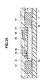
- FIG. 29 is a sectional view of a fabrication step following FIG. 28;
- FIG. 30 is a sectional view of a fabrication step following FIG. 29;
- FIG. 31 is a sectional view of a semiconductor device according to the ninth embodiment of the present invention.
- FIG. 32 is a sectional view of a semiconductor device according to the 10th embodiment of the present invention.
- FIG. 33 is a sectional view of a first sample used in a shear strength test
- FIG. 34 is a sectional view of a second sample used in the shear strength test.
- FIG. 35 is a sectional view of a comparative sample used in a shear strength test.
- FIG. 36 is an enlarged sectional view of a conventional semiconductor device.
- FIG. 1 is a sectional view showing a semiconductor device according to the first embodiment of the present invention.
- This semiconductor device includes a planar square base plate 1 made of, e.g., silicon, glass, ceramics, resin, or metal.
- an adhesive layer 2 made of, e.g., an adhesive, self-adhesive sheet, or double-coated adhesive tape is formed.
- the lower surface of a silicon substrate (semiconductor substrate) 4 of a planar square semiconductor structure 3 slightly smaller than the base plate 1 is adhered to a central portion of the upper surface of the adhesive layer 2 .
- a central portion of the upper surface of a silicon substrate 4 defines an integrated circuit region (not shown) in which an integrated circuit or circuits such as a storage circuit or control circuit are formed.
- an integrated circuit or circuits such as a storage circuit or control circuit are formed.
- a plurality of connecting pads 5 connected to predetermined elements in the integrated circuit region via lines (not shown) and made of an aluminum-based metal or the like are formed.
- a number of connecting pads 5 are formed on a silicon substrate 4 , only a couple of connecting pad 5 are shown in FIG. 1 to simplify a drawing.
- the semiconductor structure 3 is usually called a semiconductor chip.
- the semiconductor structure 3 has the silicon substrate 4 having a semiconductor circuit region, the connecting pads 5 formed on the upper surface of the silicon substrate 4 , and an insulating layer 6 covering the entire upper surface of the silicon substrate 4 and having holes 7 which expose central portions of the connecting pads 5 .
- a first insulating layer 8 (lower insulating layer) made of, e.g., polyimide or an epoxy-based resin is formed on the upper surface of the adhesive layer 2 and on the upper surface of the semiconductor structure 3 . Holes 9 are formed in those portions of the first insulating layer 8 , which correspond to the holes 7 in the insulating layer 6 . From the upper surface of each connecting pad 5 exposed through the holes 7 and 9 to predetermined portion of the upper surface of the first insulating layer 8 , a first upper distributing line 10 made up of a first metal undercoating 10 a and a first upper metal layer 10 b formed on the first metal undercoating 10 a is formed.
- the first metal undercoating 10 a has a two-layered structure including a titanium layer and a copper layer on the titanium layer.
- the first upper metal layer 10 b is made of a copper layer alone.
- Columnar electrodes 11 made of copper are formed on the upper surfaces of connecting pad portions of the first upper distributing lines 10 .
- a second insulating layer 12 made of, e.g., polyimide or an epoxy-based resin is formed such that the upper surface of the second insulating layer 12 is leveled with the upper surfaces of the columnar electrodes 11 . Accordingly, the upper surfaces of the columnar electrodes 11 are exposed from the second insulating layer 12 .
- a second upper distributing line 13 made up of a second metal undercoating 13 a and a second upper metal layer 13 b formed on the second metal undercoating 13 a is formed.
- the second metal undercoating 13 a also has a two-layered structure including a titanium layer and a copper layer on the titanium layer.
- the second upper metal layer 13 b is made of a copper layer alone.
- a cupric oxide layer 14 is formed on the inside, and a cuprous oxide layer 15 is formed on the outside.
- a hole 16 which exposes a portion of the upper surface of the second upper metal layer 13 b outside is formed through the cupric oxide layer 14 and cuprous oxide layer 15 covering the upper surface of each second upper distributing line 13 .
- the portion of the second upper distributing line 13 which is exposed from the hole 16 forms a connecting pad portion.
- a third insulating layer (encapsulating layer) 17 made of, e.g., polyimide or an epoxy-based resin is formed. Holes 18 are formed in those portions of the third insulating layer 17 , which correspond to the connecting pad portions of the second upper distributing lines 13 . In and above the holes 16 and 18 , solder balls (low-melting metal) 19 are formed and electrically connected to the connecting pad portions of the second upper distributing lines 13 . The solder balls 19 are arranged in a matrix manner on the third insulating layer 17 .
- the base plate 1 is made slightly larger than the semiconductor structure 3 in order to make the formation region of the solder balls 19 slightly larger than the planar size of the semiconductor structure 3 in accordance with an increase in number of the connecting pads 5 on the silicon substrate 4 , thereby making the planar size and interval of the connecting pad portions of the second upper distributing lines 13 larger than the planar size and interval of the connecting pads 5 on the silicon substrate 4 .
- those connecting pad portions of the second upper distributing lines 13 which are arranged in a matrix manner are formed not only in a region corresponding to the semiconductor structure 3 but also in that region formed outside the side surfaces of the semiconductor structure 3 , which corresponds to the first insulting layer 8 . That is, of the solder balls 19 arranged in a matrix manner, at least outermost solder ball or balls 19 are formed in a peripheral portion outside the semiconductor structure 3 .
- an adhesive layer 2 is formed on the entire upper surface of a large base plate having a size from which a plurality of small base plates 1 can be obtained (this large base plate is denoted by the same reference numeral 1 as the small base plate for the sake of convenience). Then, the lower surfaces of silicon substrates 4 of semiconductor structures 3 are adhered to a plurality of predetermined portions of the upper surface of the adhesive layer 2 .
- a first insulating layer 8 made of, e.g., polyimide or an epoxy-based resin is formed on the upper surface of the adhesive layer 2 and on the semiconductor structures 3 .
- the upper surface of the first insulating layer 8 is flat, and holes 9 are formed in those portions of the first insulating layer 8 , which correspond to holes 7 in the semiconductor structures 3 .
- a first metal undercoating 10 a is formed on the entire upper surface of the first insulating layer 8 and on the upper portions of connecting pods 5 exposed through the holes 7 and 9 .
- a layer forming first metal undercoatings 10 a is obtained by forming a titanium layer by sputtering and forming a copper layer on this titanium layer by sputtering.
- a known photolithography technique is used to form a plating resist layer 21 on the upper surface of the first metal undercoating 10 a by patterning.
- holes 22 are formed in prospective regions of first upper distributing lines 10 by the patterning of the plating resist layer 21 .
- the layer forming first metal undercoatings 10 a is then used as a plating current path to perform electroplating of copper, thereby forming first upper metal layers 10 b on the upper surfaces of those portions of the first metal undercoating 10 a, which are exposed in the holes 22 of the plating resist layer 21 . After that, the plating resist layer 21 is removed.
- photolithography is used again to form a plating resist film 23 by patterning on the layer forming the first metal undercoatings 10 a and on the upper surfaces of the first metal layers 10 b.
- holes 24 are formed in regions corresponding to connecting pad portions of the first upper metal layers 10 b by the patterning of the plating resist film 23 .
- the layer forming the first metal undercoatings 10 a is used as a plating current path to perform electroplating of copper, thereby forming columnar electrodes 11 on the upper surfaces of the connecting pad portions of the first upper metal layers 10 b in the holes 24 of the plating resist film 23 .
- First upper distributing lines 10 are formed by the first metal undercoatings 10 a and the first upper metal layers 10 b formed on the entire upper surfaces of the first metal undercoatings 10 a.
- a second insulating layer 12 made of, e.g., polyimide or an epoxy-based resin is so formed as to have a thickness slightly larger than the height of the columnar electrodes 11 .
- the upper surfaces of the columnar electrodes 11 are covered with the second insulating layer 12 .
- the second insulating layer 12 and the upper surfaces of the columnar electrodes 11 are appropriately polished. Consequently, as shown in FIG. 8, the upper surfaces of the columnar electrodes 11 are leveled with and exposed from the second insulating layer 12 .
- a layer forming second metal undercoatings 13 a is formed on the entire upper surface of the second insulating layer 12 and on the upper surfaces of the columnar electrodes 11 .
- the layer forming the second metal undercoatings 13 a is obtained by forming a titanium layer by sputtering and forming a copper layer on this titanium layer by sputtering.
- photolithography is used to form a plating resist layer 25 on the upper surface of the layer forming the second metal undercoatings 13 a by patterning.
- This pattern of the plating resist layer 25 has holes 26 formed in regions corresponding to prospective regions of second upper distributing lines 13 .
- the layer forming the second metal undercoatings 13 a is used as a plating current path to perform electroplating of copper, thereby forming second upper metal layers 13 b on the upper surfaces of the layer forming the second metal undercoatings 13 a in the holes 26 of the plating resist layer 25 .
- the second upper metal layers 13 b are used as masks to etch away unnecessary portions of the layer forming the second metal undercoatings 13 a. Consequently, as shown in FIG. 10, the second metal undercoatings 13 a remain only below the second upper metal layers 13 b.
- Second upper distributing lines 13 are formed by the remaining second metal undercoatings 13 a and the second upper metal layers 13 b formed on the entire surfaces of the second metal undercoatings 13 a.
- the titanium layer thickness of the first and second metal undercoatings 10 a and 13 a is about 100 to 200 nm, and the copper layer thickness of these undercoatings is about 300 to 600 nm.
- the thickness of each of the first and second upper metal layers 10 b and 13 b is about 1 to 10 ⁇ m.
- the height of the columnar electrode 11 is about 100 to 150 ⁇ m.
- a resist film 27 made of a dry layer or liquid photoresist is formed on the upper surface of a connecting pad portion of each second upper distributing line 13 .
- the resist film 27 is used as a mask to form an oxide layer on the side surfaces of the copper layer of each second metal undercoating 13 a and on the surface of each second upper metal layer 13 b made of copper. No oxide layer is formed on a portion of each second upper distributing line 13 where the resist film 27 is formed, so this portion functions as a connecting pad.
- the first method is to form a cupric oxide layer
- the second method is to form a cuprous oxide layer on the cupric oxide layer.
- the first method of forming a cupric oxide layer will be described first.
- washing or the like is performed after the above fabrication step, i.e., the wet etching step of etching away unnecessary portions of the layer to form second metal undercoatings 13 a by using the second upper metal layers 13 b as masks.
- the wet etching step of etching away unnecessary portions of the layer to form second metal undercoatings 13 a by using the second upper metal layers 13 b as masks.
- natural copper oxide nonuniformly produced on the side surfaces of the copper layers of the second metal undercoatings 13 a and on the surfaces of the second upper metal layers 13 b is removed by dipping into sulfuric acid.
- washing and drying are performed to form a pure copper surface as the surface of each second upper distributing line 13 .
- the silicon substrates 4 and the like are inserted together with a support jig into a chamber of an oven (not shown), and prebaking is performed in a nitrogen gas ambient at about 165° C. for about 45 min. This prebaking is performed so that the temperatures of parts such as the silicon substrates 4 and the support jig are evenly set at a preset temperature of about 165° C. Since the process is performed in a nitrogen gas ambient, no copper oxide is formed on the surfaces of the second upper distributing lines 13 and the like.
- the prebaked silicon substrate 4 and the like are transferred into a chamber of a vacuum oven (not shown), and main baking is performed.
- the chamber is evacuated from the atmospheric pressure to about 133 Pa at a temperature of about 165° C., and dry air is supplied to restore the atmospheric pressure.
- This cycle is repeated three times.
- annealing is performed in the dry air ambient at about 165° C. for about 10 min.
- a cupric oxide layer 14 about 20 to 40 nm thick is formed on the side surfaces of the copper layer of the second metal undercoating 13 a and on the surface of the second upper metal layer 13 b.
- 100% oxygen gas may also be used in place of the dry air.
- washing or the like is performed after the above fabrication step, i.e., the wet etching step of etching away unnecessary portions of the layer to form second metal undercoatings 13 a by using the second upper metal layers 13 b as masks.
- the wet etching step of etching away unnecessary portions of the layer to form second metal undercoatings 13 a by using the second upper metal layers 13 b as masks.
- natural copper oxide nonuniformly produced on the side surfaces of the copper layers of the second metal undercoatings 13 a and on the surfaces of the second upper metal layers 13 b is removed by dipping into sulfuric acid.
- washing and drying are performed to form a pure copper surface as the surface of each second upper distributing line 13 .
- a first processing solution contains about 10 to 20 wt % of sodium hydroxide and about 80 to 90 wt % of pure water.
- a second solution contains about 15 to 25 wt % of sodium chlorite, about 70 to 80 wt % of pure water, and about 1 to 10 wt % of a stabilizer.
- the base plate 1 and the like are dipped in a solution mixture of about 30 to 40 mL/L of the first processing solution and about 960 to 970 mL/L of pure water (the total of the two solutions is 1,000 mL/L) at room temperature for about 1 to 2 min.
- This dipping process is performed to adapt the second upper distributing lines 13 to a processing solution (solution mixture) in the next dipping process, and no copper oxide is formed on the surfaces of the second upper distributing lines 13 .
- the base plate 1 and the like are dipped in a solution mixture of about 50 mL/L of the first processing solution, about 450 mL/L of the second processing solution, and about 500 mL/L of pure water at about 55° C. for about 1 min. After that, water washing, hot water washing, and drying are performed. Consequently, a cupric oxide layer 14 about 50 to 500 nm thick is formed on the side surfaces of the copper layer of each second metal undercoating 13 a and on the surface of each second upper metal layer 13 b, and a cuprous oxide layer 15 about 10 to 100 nm thick is formed on the surface of the cupric oxide layer 14 . Then, the resist film 27 is removed.
- a third insulating layer 17 made of, e.g., polyimide or an epoxy-based resin is used to form a third insulating layer 17 made of, e.g., polyimide or an epoxy-based resin by patterning on the surface of the second insulating layer 12 and on the cupric oxide layers 14 and cuprous oxide layers 15 on the surfaces of the second upper distributing lines 13 .
- holes 18 are formed in regions corresponding to those portions of the third insulating layer 17 , which correspond to holes 16 in the cupric oxide layers 14 and cuprous oxide layers 15 .
- solder balls 19 are formed in and above the holes 16 and 18 so as to be connected electrically and mechanically to the connecting pad portions of the second upper distributing lines 13 .
- the three insulating layers 17 , 12 , and 8 , the adhesive layer 2 , and the base plate 1 are cut between adjacent semiconductor structures 3 to obtain a plurality of semiconductor devices shown in FIG. 1 .
- the effect of the oxide layer will be described below on the basis of a shear strength test conducted by a pressure cooker test (PCT).
- PCT pressure cooker test
- the first semiconductor device 230 had a structure in which a polyimide protective layer 208 , and a distributing line 213 made up of a two-layered metal undercoating 213 a including a titanium layer and copper layer and an upper metal layer 213 b made of copper were formed on a silicon substrate 204 , and a cupric oxide layer 214 was formed on the side surfaces of the copper layer of the metal undercoating 213 a and on the surface of the upper metal layer 213 b.
- the second semiconductor device 330 had a structure in which a polyimide protective layer 308 , and a distributing line 313 made up of a two-layered metal undercoating 313 a including a titanium layer and copper layer and an upper metal layer 313 b made of copper were formed below a silicon substrate 304 , and a cupric oxide layer 314 was formed on the side surfaces of the copper layer of the metal undercoating 313 a and on the surface of the upper metal layer 313 b.
- the second sample had a structure in which a second semiconductor device 330 was attached to a central portion of the upper surface of a first semiconductor device 230 via an insulating layer 217 made of an epoxy-based resin.
- the first semiconductor device 230 had a structure in which a polyimide protective layer 208 , and a distributing line 213 made up of a two-layered metal undercoating 213 a including a titanium layer and copper layer and an upper metal layer 213 b made of copper were formed on a silicon substrate 204 .
- a cupric oxide layer 214 was formed on the side surfaces of the copper layer of the metal undercoating 213 a and on the surface of the upper metal layer 213 b, and a cuprous oxide layer 215 was stacked on the cupric oxide layer 214 .
- the second semiconductor device 330 had a structure in which a polyimide protective layer 308 , and a distributing line 313 made up of a two-layered metal undercoating 313 a including a titanium layer and copper layer, and an upper metal layer 313 b made of copper were formed below a silicon substrate 304 .
- a cupric oxide layer 314 was formed on the side surfaces of the copper layer of the metal undercoating 313 a and on the surface of the upper metal layer 313 b, and a cuprous oxide layer 315 was stacked on the cupric oxide layer 314 .
- a comparative sample shown in FIG. 35 was also prepared.
- This comparative sample had a structure in which a second semiconductor device 330 was attached to a central portion of the upper surface of a first semiconductor device 230 via an insulating layer 217 made of an epoxy-based resin.
- a cupric oxide layer nor a cuprous oxide layer was formed on either of the distributing lines 213 and 313 .
- the rest of the arrangement is the same as the first and second samples. Therefore, the same reference numerals denote the same parts, and a detailed explanation thereof will be omitted.
- the cupric oxide layer 314 of the second semiconductor device 330 was adhered to the central portion of the upper surface of the cupric oxide layer 214 of the first semiconductor device 230 via the insulating layer 217 .
- the cuprous oxide layer 315 of the second semiconductor device 330 was adhered to the central portion of the upper surface of the cuprous oxide layer 215 of the first semiconductor device 230 via the insulating layer 217 .
- the distributing line 313 of the second semiconductor device 330 was directly adhered to the central portion of the upper surface of the distributing line 213 of the first semiconductor device 230 via the insulating layer 217 .
- the dimensions of the first, second, and comparative samples will be described below.
- the first semiconductor device 230 had a planar size of 8 ⁇ 8 mm and a total thickness of 0.75 mm.
- the second semiconductor device 330 had a planar size of 2 ⁇ 2 mm and a total thickness of 0.75 mm.
- the insulating layer 217 was circular and had a diameter of 1.5 mm and a thickness of 0.03 mm.
- a shearing force measurement jig (not shown) was pushed against the side surface of the second semiconductor device 330 , and the shear strength (N/mm 2 ) was calculated by dividing the load when the second semiconductor device 330 peeled off by the adhesion area (an area of 1.77 mm 2 of the insulating layer 217 ). More specifically, the shear strength immediately after the insulating layer 217 made of an epoxy-based resin was thermoset and the shear strength when 30 hrs had elapsed after thermosetting were calculated.
- the shear strength of the comparative sample was 31.60 N/mm 2 immediately after thermosetting and 11.86 N/mm after the elapse of 30 hrs.
- the shear strength of the first sample was 49.15 N/mm 2 immediately after thermosetting, which was about 1.55 times that of the comparative sample, and was 38.41 N/mm 2 after the elapse of 30 hrs, which was about 3.24 times that of the comparative sample.
- the shear strength of the second sample was 66.10 N/mm 2 immediately after thermosetting, which was about 1.34 times that of the comparative sample, and was 58.76 N/mm 2 after the elapse of 30 hrs, which was about 1.53 times that of the comparative sample.
- the above test results indicate that the adhesion of the insulating layer 217 made of an epoxy-based resin to the cupric oxide layer 214 increased compared to that when only the distributing line 213 , i.e., only the copper layer was formed. Also, the adhesion when the cupric oxide layer 214 and cuprous oxide layer 215 were formed was higher than that when only the cupric oxide layer 214 was formed.
- the cupric oxide layer 14 or the stacked structure of the cupric oxide layer 14 and cuprous oxide layer 15 was formed on the side surfaces of the copper layer of the second metal undercoating 13 a and on the surface of the second upper metal layer 13 b.
- the adhesion of the interface between the second upper distributing line 13 and the natural copper oxide is generally weak. This causes peeling of the third insulating layer 17 made of polyimide, an epoxy-based resin or the like, formed on the surface of the second upper distributing line 13 , resulting in an insufficient humidity resistance.
- the adhesion of the interface between the second upper distributing line 13 and the cupric oxide layer 14 is strong.
- the anchor effect increases the adhesion of the interface between the cuprous copper layer 15 and the third insulating layer 17 .
- the third insulating layer 17 does not easily peel off any longer, so the humidity resistance can be increased.
- the first metal undercoating 10 a and first upper metal layer 10 b to be connected to the connecting pad 5 of the semiconductor structure 3 are formed by sputtering and electroplating
- the columnar electrode 11 to be connected to the connecting pad portion of the first upper distributing line 10 is formed by electroplating
- the second metal undercoating 13 a and second upper metal layer 13 b to be connected to the upper surface of the columnar electrode 11 are formed by sputtering and electroplating.
- the columnar electrode 11 of about 100 to 150 ⁇ m high is formed between the first and second upper distributing lines 10 and 13 . Therefore, when the semiconductor device is bonded to a circuit board (not shown), concentrated stress produced by the difference between the linear expansion coefficients of the semiconductor structure 3 and circuit board can be absorbed by shaking of the columnar electrode 11 .
- the semiconductor structures 3 are adhered to a plurality of predetermined portions on the adhesive layer 2 on the base plate 1 , and the first to third insulating layers 8 , 12 , and 17 , the first and second distributing lines 10 and 13 , the columnar electrodes 11 , and the solder balls 19 are formed for the semiconductor structures 3 at once. After that, the resultant structure is cut into a plurality of semiconductor devices. This simplifies the fabrication process.
- a plurality of semiconductor structures 3 can be transferred together with the base plate 1 , and this also simplifies the fabrication process. Furthermore, when the base plate 1 is given predetermined outer dimensions, a common transfer system can be used regardless of the outer dimensions of semiconductor devices to be fabricated.
- an aqueous solution of sodium chlorite in the second processing solution is an oxidizing alkali solution which is strong alkali having a pH of 12 or more. Therefore, if the processing temperature is about 55° C., this solution dissolves the silicon substrate 4 , so the processing time is as short as possible. In the above embodiment, the processing time is about 1 min.
- an adhesive layer 32 made of an ultraviolet-curing self-adhesive sheet or the like is adhered to the entire upper surface of a lower base plate 31 such as an ultraviolet-transmitting transparent resin plate or glass plate, and a base plate 1 and adhesive layer 2 described above are adhered to the upper surface of the adhesive layer 32 .
- the adhesive layer 2 , the base plate 1 , and the adhesive layer 32 are cut between adjacent semiconductor structures 3 , and the adhesive layer 32 and the lower base plate 31 is left uncut.
- Ultraviolet radiation is emitted from the lower surface of the lower base plate 31 , thereby curing the adhesive layer 32 .
- the divided semiconductor devices on the adhesive layer 32 are peeled and picked up one by one to obtain a plurality of semiconductor devices shown in FIG. 1 .
- the divided semiconductor devices on the adhesive layer 32 are not yet separated. Therefore, these semiconductor devices can be peeled and picked up one by one when they are mounted on a circuit board (not shown), without using any dedicated semiconductor device tray. Also, when the adhesive layer 32 remaining on the upper surface of the lower base plate 31 and having low adhesion is peeled, the lower base plate 31 can be reused. Furthermore, when base plates 1 are given predetermined outer dimensions, a common transfer system can be used regardless of the outer dimensions of semiconductor devices to be fabricated. Note that a thermosetting self-adhesive sheet or the like may also be used as the adhesive layer 32 in some cases.
- the lower base plate 31 it is also possible to use a common dicing tape from which semiconductor devices are removed by expansion.
- the adhesive layer need not be ultraviolet-curing.
- the lower base plate 31 may also be removed by polishing or etching.
- FIG. 16 A second modification of the fabrication method of the semiconductor device shown in FIG. 1 will be described below.
- a layer forming second metal undercoatings 13 a is formed by electroless plating of copper on the entire upper surface of a second insulating layer 12 including the upper surfaces of columnar electrodes 11 .
- the layer for the second metal undercoatings 13 a is used as a plating current path to perform electroplating of copper, thereby forming a second upper metal layer formation layer 13 c on the entire upper surface of the layer for second metal undercoatings 13 a.
- a resist layer 33 is then formed by patterning on those portions of the upper surface of the second upper metal layer formation layer 13 c, which correspond to prospective second distributing line regions.
- the resist layer 33 is used as a mask to etch away unnecessary portions of the second upper metal layer formation layer 13 c and the layer for second metal undercoatings 13 a. Consequently, as shown in FIG. 17, second upper distributing lines 13 are left behind only below the resist layer 33 . After that, the resist layer 33 is removed.
- the base plate 1 shown in FIG. 2 or the lower base plate 31 shown in FIG. 14 can also be a tray. That is, the base plate is formed into a shape like a saucer in which an array region of semiconductor structures 3 is depressed from the surrounding. A plating current path metal layer is formed on the upper surface surrounding the array region of semiconductor structures 3 of this tray-like base plate and connected to plating current path metal undercoatings ( 10 a and 13 a ) by a conductive member, thereby performing electroplating.
- trays are given predetermined outer dimensions, the same fabrication apparatus can be used even when the sizes of semiconductor devices to be fabricated are different. This increases the fabrication efficiency.
- the lower surface of the silicon substrate 4 is adhered to the upper surface of the base plate 1 via the adhesive layer 2 , and the side surfaces and the like of the silicon substrate 4 are bonded to the upper surface of the base plate 1 via a first insulating layer 8 . Therefore, the bonding strength of the semiconductor structure 3 to the base plate 1 can be increased to a certain extent.
- FIG. 19 is a sectional view of a semiconductor device according to the third embodiment of the present invention. This semiconductor device differs from the semiconductor device shown in FIG. 1 in that the device has neither a base plate 1 nor an adhesive layer 2 .
- solder balls 19 are formed as shown in FIG. 12, a base plate 1 and adhesive layer 2 are removed by polishing or etching. After that, three insulating layers 17 , 12 , and 8 are cut between adjacent semiconductor structures 3 to obtain a plurality of semiconductor devices shown in FIG. 19 .
- the semiconductor device thus obtained can be made thin because it has neither a base plate 1 nor an adhesive layer 2 .
- a base plate 1 and adhesive layer 2 are removed by polishing or etching to form a semiconductor device shown in FIG. 19 .
- the lower surfaces of a silicon substrate 4 and first insulating layer 8 are appropriately polished.
- three insulating layers 17 , 12 and 8 are cut between adjacent semiconductor structures 3 to obtain a plurality of semiconductor devices according to the fourth embodiment of the present invention shown in FIG. 20 .
- This semiconductor device can be made thinner.
- solder balls 19 it is also possible to remove the base plate 1 and adhesive layer 2 by polishing or etching (and, if necessary, appropriately polish the lower surfaces of the silicon substrate 4 and first insulating layer 8 ) before solder balls 19 are formed, form solder balls 19 after that, and then cut the three insulating layers 17 , 12 and 8 between the adjacent semiconductor devices 3 .
- FIG. 21 is a sectional view of a semiconductor device according to the fifth embodiment of the present invention.
- This semiconductor device differs from the semiconductor device shown in FIG. 1 in that a heat-radiating metal layer 34 is adhered to the lower surface of an adhesive layer 2 .
- the metal layer 34 is made of, e.g., a copper foil having a thickness of several tens ⁇ m.
- solder balls 19 are formed as shown in, e.g., FIG. 12, a base plate 1 is removed by polishing or etching, and a metal layer 34 is adhered to the entire lower surface of an adhesive layer 2 . After that, three insulating layers 17 , 12 and 8 , the adhesive layer 2 , and the metal layer 34 are cut between adjacent semiconductor structures 3 to obtain a plurality of semiconductor devices shown in FIG. 21 .
- FIG. 22 is a sectional view of a semiconductor device according to the sixth embodiment of the present invention.
- a package generally called a wafer level (WL) CSP is used as a semiconductor structure 41 on a base plate 1
- the columnar electrode 11 shown in FIG. 1 is not formed on the WLCSP
- a second upper distributing line 13 is connected to a connecting pad portion of a first upper distributing line 10 through a hole 12 a formed in a second insulating layer 12 .
- the semiconductor structure 41 is called a WLCSP, and includes a silicon substrate 4 adhered to a central portion of the upper surface of an adhesive layer 2 formed on the base plate 1 .
- An integrated circuit portion (not shown) is formed in a central portion of the upper surface of the silicon substrate 4 .
- a plurality of connecting pads 5 made of an aluminum-based metal or the like are formed and electrically connected to the integrated circuit portion.
- An insulating layer 6 made of silicon oxide or the like is formed on the upper surface of the silicon substrate 4 except for central portions of the connecting pads 5 . These central portions of the connecting pads 5 are exposed through holes 7 formed in the insulating layer 6 .
- the structure up to this point is the same as the semiconductor structure 3 shown in FIG. 1 .
- a protective layer 42 made of, e.g., polyimide or an epoxy-based resin is additionally formed on the upper surface of the insulating layer 6 .
- Holes 43 are formed in those portions of the protective layer 42 , which correspond to holes 7 in the insulating layer 6 .
- Distributing lines (lower distributing lines) 44 are formed from the upper surfaces of the connecting pads 5 exposed through the holes 7 and 43 to predetermined portions of the upper surface of the protective layer 42 .
- Each distributing line 44 is made up of a metal undercoating 44 a made of copper or the like and an upper metal layer 44 b formed on the metal undercoating 44 a and made of copper.
- Columnar electrodes 45 made of copper are formed on the upper surfaces of connecting pad portions of the distributing lines 44 .
- a lower encapsulating layer 46 made of, e.g., polyimide or an epoxy-based resin is formed on the upper surface of the protective layer 42 including the distributing lines 44 such that the upper surface of the lower encapsulating layer 46 is leveled with the upper surfaces of the columnar electrodes 45 .
- the semiconductor structure 41 of this embodiment includes the silicon substrate 4 , connecting pads 5 , and insulating layer 6 , and further includes the protective layer 42 , distributing lines 44 , columnar electrodes 45 , and lower encapsulating layer 46 .
- a side insulating layer 47 made of, e.g., polyimide or an epoxy-based resin is formed such that the upper surface of the side insulating layer 47 is leveled with the upper surface of the lower encapsulating layer 46 .
- a first insulating layer 8 made of, e.g., polyimide or an epoxy-based resin is formed on the upper surfaces of the side insulating layer 47 and columnar electrodes 45 . Holes 8 a are formed in those portions of the first insulating layer 8 , which correspond to central portions of the upper surfaces of the columnar electrodes 45 .
- First distributing lines 10 are formed from the upper surfaces of the columnar electrodes 45 exposed through the holes 8 a to predetermined portions of the upper surface of the first insulating layer 8 .
- the arrangement of a portion above the first insulting layer 8 including the first upper distributing lines 10 is substantially the same as shown in FIG. 1, so a detailed explanation thereof will be omitted. As described above, however, this embodiment does not include the columnar electrodes 11 shown in FIG. 1 . Instead, second upper distributing lines 13 are connected to the connecting pad portions of the first upper distributing lines 10 through the holes 12 a formed in the second insulating layer 12 .
- a wafer-like semiconductor substrate (a silicon substrate 4 before being cut) on which connecting pads 5 , an insulating layer 6 , and a protective layer 42 are formed is prepared.
- a layer forming lower metal layers 44 a is formed by electroless plating or sputtering on the entire upper surface of the protective layer 42 including the upper surfaces of the connecting pads 5 exposed in holes 7 and 43 .
- upper metal layers 44 b are formed by electroplating on predetermined portions of the upper surface of the layer of the metal undercoatings 44 a.
- Columnar electrodes 45 are formed by electroplating on the upper surfaces of connecting pad portions of the upper metal layers 44 b.
- the columnar electrodes 45 and upper metal layers 44 b are used as masks to etch away unnecessary portions of the layer for the metal undercoatings 44 a so that the metal undercoatings 44 a remain only below the upper metal layers 44 b, thereby forming distributing lines 44 made up of the remaining metal undercoatings 44 a and the upper metal layers 44 b formed on the entire upper surfaces of the metal undercoatings 44 a.
- a lower encapsulating layer 46 is so formed as to have a thickness larger than the height of the columnar electrodes 45 .
- the upper surfaces of the columnar electrodes 45 are covered with the lower encapsulating layer 46 .
- the upper surfaces of the lower encapsulating layer 46 and columnar electrodes 45 are appropriately polished to expose the upper surfaces of the columnar electrodes 45 .
- a plurality of semiconductor structures 41 shown in FIG. 22 are obtained.
- the columnar electrodes 45 have a height of about 100 to 150 ⁇ m.
- an adhesive layer 2 is formed on the entire upper surface of a large base plate from which a plurality of small base plates 1 shown in FIG. 22 can be obtained.
- the lower surfaces of silicon substrates 4 of semiconductor structures 41 are adhered to a plurality of predetermined portions of the upper surface of the adhesive layer 2 .
- a side insulating layer 47 made of, e.g., polyimide or an epoxy-based resin is formed on the upper surface of the adhesive layer 2 including the semiconductor structures 41 such that the thickness of the side insulating layer 47 is slightly larger than the height of the semiconductor structures 41 .
- the upper surfaces of the semiconductor structures 41 are covered with the side insulating layer 47 .
- the upper surfaces of the side insulating layer 47 and columnar electrodes 45 are appropriately polished to expose the upper surfaces of columnar electrodes 45 of the semiconductor structures 41 .
- a lower encapsulating layer 46 is formed on the upper surface of a protective layer 42 including the columnar electrodes 45 and distributing lines 44 such that the thickness of the lower encapsulating layer 46 is slightly larger than the height of the columnar electrodes 45 .
- the upper surfaces of the lower encapsulating layer 46 and columnar electrodes 45 are appropriately polished so that the upper surfaces of the columnar electrodes 45 are leveled with the upper surface of the encapsulating layer 46 . Accordingly, two polishing steps are performed.
- a method by which only one polishing step need be performed will be described below.
- a semiconductor structure 41 having no lower encapsulating layer 46 in the state shown in FIG. 23 is prepared. That is, after a protective layer 42 , distributing lines 44 , and columnar electrodes 45 are formed on a wafer-like semiconductor substrate on which connecting pads 5 and an insulating layer 6 are formed, the semiconductor substrate is diced without forming a lower encapsulating layer 46 .
- a lower encapsulating layer 46 and side insulating layer 47 are simultaneously formed by the same encapsulating material in prospective regions of these layers, and the upper surfaces of the columnar electrodes 45 are polished together with the lower encapsulating layer 46 and side insulating layer 47 (there is no boundary between these layers because they are integrated). That is, the encapsulating layer formation step is performed only once, so the polishing step need only be performed once.
- the heights of the columnar electrodes 45 of the semiconductor structure 41 in the state shown in FIG. 23 vary because the columnar electrodes 45 are formed by electroplating.
- the polishing step is performed twice, the semiconductor structure 41 in the state shown in FIG. 23 has a uniform height. That is, the height of the semiconductor structure 41 in the state shown in FIG. 23 can be made uniform beforehand.
- a first insulating layer 8 made of, e.g., polyimide or an epoxy-based resin is formed on the upper surfaces of the lower encapsulating layer 46 , side insulating layer 47 , and columnar electrodes 45 on the same level.
- holes 8 a are formed in those portions of the first insulating layer 8 , which correspond to central portions of the upper surfaces of the columnar electrodes 45 .
- first upper distributing lines 10 are formed by plating on predetermined portions of the upper surface of the first insulating layer 8 and on the upper surfaces of the columnar electrodes 45 exposed through the holes 8 a, and a second insulating layer 12 having holes 12 a is formed.
- Second upper distributing lines 13 are formed on predetermined portions of the upper surface of the second insulating layer 12 and on the upper surfaces of connecting pad portions of the first upper distributing lines 10 exposed through the holes 12 a.
- Cupric oxide layers 14 and cuprous oxide layers 15 are formed in this order on the surfaces of the second upper distributing lines 13 except for their connecting pad portions.
- a third insulating layer 17 having holes 18 is formed, and solder balls 19 are formed. Then, the three insulating layers 17 , 12 and 8 , side insulating layer 47 , adhesive layer 2 , and base plate 1 are cut between adjacent semiconductor structures 41 to obtain a plurality of semiconductor devices shown in FIG. 22 .
- the first upper distributing lines 10 are directly bonded onto the columnar electrodes 45 by plating. Therefore, the hole 8 a in the first insulating layer 8 is sufficiently strong if the hole 8 a is a square or circular hole having an area of at least 10 ⁇ m ⁇ 10 ⁇ m.
- An aligner of this type has an alignment accuracy of several tens ⁇ m, and the diameter of a circular columnar electrode is usually about 100 to 150 ⁇ m (the pitch is usually twice this value).
- connecting the columnar electrodes and distributing lines by plating can be applied even when the size and interval of the columnar electrodes are very small, and the process is also efficient.
- the width or diameter of the hole 8 a formed in the first insulating layer 8 to connect the first upper distributing line 10 to the columnar electrode 45 can be 1 ⁇ 2 or less the width or diameter of the columnar electrode 45 . Since this decreases the size and interval of the columnar electrodes 45 of the semiconductor structure 41 , a semiconductor device having upper distributing lines such as the first upper distributing lines 10 can be further downsized.
- FIG. 26 is a sectional view of a semiconductor device according to the seventh embodiment of the present invention. Compared to the semiconductor structure 41 shown in FIG. 22, a semiconductor structure 41 of this semiconductor device has no columnar electrodes 45 , and holes 46 a are formed in those portions of a lower encapsulating layer 46 , which correspond to connecting pad portions of distributing lines 44 .
- first upper distributing lines 10 are connected to the connecting pad portions of the distributing lines 44 through holes 8 b in a first insulating layer 8 and the holes 46 a in the lower encapsulating layer 46 .
- Cupric oxide layers 14 and cuprous oxide layers 15 are formed in this order on the surfaces of the first upper distributing lines 10 except for their connecting pad portions.
- Solder balls 19 are formed in holes 12 b in a second insulating layer 12 which is formed on the copper oxide layers 14 and 15 , and in holes 16 in the copper oxide layers 14 and 15 , so as to be connected to the connecting pad portions of the first upper distributing lines 10 .
- the semiconductor structure 41 need not have any columnar electrodes, i.e., need only have the distributing lines 44 .
- the upper distributing line may also be one layer, i.e., the first upper distributing line 10 (in this case, the second insulating layer 12 is an overcoat layer).
- three or more upper distributing line layers may also be formed. A method of forming three upper distributing line layers will be briefly described below.
- a third insulating layer (denoted by reference numeral 17 in FIG. 1) is formed on a second insulating layer 12 , and third upper distributing lines are formed on the third insulating layer 12 .
- Cupric oxide and cuprous oxide layers are formed on the surfaces of the third upper distributing lines except for their connecting pads.
- a fourth insulating layer is formed as an overcoat layer on the cupric oxide and cuprous oxide layers.
- FIG. 27 is a sectional view of a semiconductor device according to the eighth embodiment of the present invention.
- This semiconductor device differs from the semiconductor device shown in FIG. 26 in that a semiconductor structure 41 having no lower encapsulating layer 46 is used, and a square frame-like buried member 51 having substantially the same thickness as the semiconductor structure 41 is formed on the upper surface of an adhesive layer 2 around the semiconductor structure 41 .
- the lower surface of a lattice-like buried member 51 is adhered to a predetermined portion of the upper surface of an adhesive layer 2 formed on the entire upper surface of a large base plate from which a plurality of small base plates 1 shown in FIG. 27 can be obtained.
- the lattice-like buried member 51 is obtained by forming a plurality of square openings 51 a in a matrix manner by, e.g., punching or etching in a sheet-like buried member made of silicon, glass, ceramics, resin, metal, or the like.
- the lattice-like burrier 51 may also be formed by adhering a sheet-like buried member on the entire upper surface of the adhesive layer 2 , and performing spot facing.
- the lower surface of a silicon substrate 4 of a semiconductor structure 41 is adhered to a central portion of the upper surface of the adhesive layer 2 in each opening 51 a of the lattice-like buried member 51 .
- the upper surface of the buried member 51 and the upper surface of a protective layer 42 of the semiconductor structure 41 are positioned on substantially the same level.
- a relatively narrow gap 52 is formed between the semiconductor structure 41 and the square frame-like-barrier 51 formed around the semiconductor structure 41 .
- the thickness of the buried member 51 is substantially the same as the total thickness of the silicon substrate 4 , an insulating layer 6 , and the protective layer 42 .
- the thickness of the buried member 51 may also be substantially the same as the thickness of the silicon substrate 4 , the total thickness of the silicon substrate 4 and insulting layer 6 , or a thickness including the thickness of a distributing line 44 .
- a first insulating layer 8 made of, e.g., polyimide or an epoxy-based resin is so formed as to have a thickness slightly larger than the total height of the semiconductor structure 41 and distributing lines 44 . If necessary, the upper surface of the first insulating layer 8 is smoothened by appropriately polishing it. Holes 8 b are formed in those portions of the first insulating layer 8 , which correspond to connecting pad portions of the distributing lines 44 , by photolithography or CO 2 laser irradiation.
- first upper distributing lines 10 are formed on predetermined portions of the upper surface of the first insulating layer 8 and on the upper surfaces of connecting pad portions of the distributing lines 44 exposed through the holes 8 b. Cupric oxide layers 14 and cuprous oxide layers 15 are formed in this order on the surfaces of the first upper distributing lines 10 except for their connecting pad portions.
- a second insulating layer 12 having holes 12 a is formed, and solder balls 19 are formed. After that, the two insulating layers 12 and 8 , buried member 51 , adhesive layer 2 , and base plate 1 are cut between adjacent semiconductor structures 41 to obtain a plurality of semiconductor devices shown in FIG. 27 .
- the relatively narrow gap 52 is formed between the semiconductor structure 41 and the square frame-like buried member 51 formed around the semiconductor structure 41 , and the first insulating layer 8 made of, e.g., polyimide or an epoxy-based resin is formed in this gap 52 . Accordingly, the amount of the first insulting layer 8 can be reduced by the volume of the buried member 51 , compared to a structure having no barrier 51 . This makes it possible to decrease the stress caused by shrinkage upon curing of the first insulating layer 8 made of, e.g., polyimide or an epoxy-based resin, so the base plate 1 does not easily warp.
- FIG. 31 is a sectional view of a semiconductor device according to the ninth embodiment of the present invention. Large differences of this semiconductor device from the semiconductor device shown in FIG. 27 are that a semiconductor structure 41 having columnar electrodes 45 and a lower encapsulating layer 46 is used, the thickness of an insulating buried member 51 is slightly larger than that of the semiconductor structure 41 , intermediate distributing lines 53 are formed on the upper surface of the barrier 51 , and an intermediate insulating layer 54 is formed on the upper surface of the member 51 including the intermediate distributing lines 53 and on the upper surface of a first insulating layer 8 .
- the columnar electrodes 45 are connected to first upper distributing lines 10 partially embedded in holes 54 a formed in the intermediate insulating layer 54 by conductive materials 55 such as a conductive resin filled in holes 8 b formed in the first insulating layer 8 . Also, the two end portions of each intermediate distributing line 53 are connected to the first upper distributing lines 10 through the holes 54 a formed in the intermediate insulating layer 54 .
- the lower surface of a lattice-like buried member 51 is adhered to predetermined portions of the upper surface of an adhesive layer 2 formed on the entire upper surface of a large base plate from which a plurality of small base plates 1 shown in FIG. 31 can be obtained.
- Intermediate distributing lines 53 made of a copper foil or the like are formed beforehand on predetermined portions of the upper surface of the insulating buried member 51 .
- the lower surface of a silicon substrate 4 of a semiconductor structure 41 is adhered to a central portion of the upper surface of the adhesive layer 2 in each opening 51 a of the lattice-like buried material 51 .
- the upper surface of the lattice barrier 51 is slightly higher than the upper surface of a lower encapsulating layer 46 of the semiconductor structure 41 .
- a relatively narrow gap 52 is formed between the semiconductor structure 41 and the square frame-like barrier 51 formed outside the semiconductor structure 41 .
- a first insulating layer 8 made of, e.g., polyimide or an epoxy-based resin is so formed as to be slightly higher than the intermediate distributing lines 53 by using a metal mask or the like or by screen printing. That portion of the uncured first insulating layer 8 , which is raised to be higher than the upper surfaces of the intermediate distributing lines 53 is removed by buffing. In this manner, the upper surface of the first insulating layer 8 is substantially leveled with the upper surfaces of the intermediate distributing lines 53 , thereby substantially planarizing the whole upper surface. After that, the first insulating layer 8 is cured.
- This polishing is performed to remove that portion of the uncured first insulating layer 8 , which is raised to be higher than the upper surfaces of the intermediate distributing lines 53 , so an inexpensive, low-accuracy buff can be used.
- the first insulating layer 8 after coating may also be temporarily cured by ultraviolet irradiation or heating in order to prevent excess polishing of the uncured first insulating layer 8 formed in the gap 52 and decrease the cure shrinkage of the first insulating layer 8 . If planarization is insufficient because the cure shrinkage of the first insulating layer 8 formed in the gap 52 is too large, coating and polishing of the encapsulating resin can be repeated.
- polishing it is also possible to flatten a portion of an inexpensive, low-accuracy endless polishing belt, and polish and smoothen, by this flattened portion, that portion of the uncured or temporarily cured first insulating layer 8 , which is raised to be higher than the upper surfaces of the intermediate distributing lines 53 , by using these upper surfaces of the intermediate distributing lines 53 as polishing limiting surfaces.
- holes 8 b are formed in those portions of the first insulating layer 8 , which correspond to columnar electrodes 45 , by photolithography or CO 2 laser irradiation.
- the holes 8 b are filled with conductive materials 55 such as conductive resins.
- An intermediate insulating layer 54 made of, e.g., polyimide or an epoxy-based resin is formed by patterning on the upper surface of the first insulating layer 8 including the conductive material 55 and on the upper surface of the buried member 51 including the intermediate distributing lines 53 .
- holes 54 a are formed in those portions of the intermediate insulating layer 54 , which correspond to the two end portions of each intermediate distributing line 53 and to the conductive materials 55 .
- first upper distributing lines 10 are formed on the two end portions of each intermediate distributing line 53 exposed through the holes 54 a, on the upper surface of each conductive material 55 , and on predetermined portions of the upper surface of the intermediate insulating layer 54 .
- Cupric oxide layers 14 and cuprous oxide layers 15 are formed in this order on the surfaces of the first upper distributing lines 10 except for their connecting pad portions.
- a second insulating layer 12 having holes 12 a is formed, and solder balls 19 are formed.
- the two insulating layers 12 and 54 , buried material 51 , adhesive layer 2 , and base plate 1 are cut between adjacent semiconductor structures 41 to obtain a plurality of semiconductor devices shown in FIG. 31 .
- copper oxide layers are formed only in distributing lines.
- the 10th embodiment shown in FIG. 32 is this embodiment.
- distributing lines 13 each made up of a metal undercoating 13 a and upper metal layer 13 b are formed. Each distributing line extends from a connecting pad 5 in a peripheral portion of the semiconductor structure 3 to a central portion of the semiconductor structure 3 .
- a connecting pad portion is formed at one end on an integrated circuit portion (not shown), and a columnar projecting electrode 60 made of copper is formed on this connecting pad portion.
- a cupric oxide layer 14 is formed on the side surfaces of a copper layer of the metal undercoating 13 a, on the surface of the upper metal layer 13 b, and on the outer peripheral surface of the columnar projecting electrode 60 , and a cuprous oxide layer 15 is formed on the surface of the cupric oxide layer 14 .
- No oxide layer is formed on the upper surface of the columnar projecting electrode 60 , so this upper surface is leveled with the upper surface of an insulating layer 17 .
- columnar projecting electrodes 60 are formed on connecting pad portions of distributing lines 13 by electroplating or the like.
- a metal undercoating 13 a is patterned into the same shape as the upper metal layer 13 b, and cupric oxide layer 14 and cuprous oxide layer 15 are formed on the entire surface including the upper surfaces of the distributing lines 13 and projecting electrodes 60 .
- an insulating layer 17 is once formed on an insulating layer 8 so as to have a thickness larger than the height of the projecting electrodes 60 .
- the cupric oxide layer 14 and cuprous oxide layer 15 on the upper surface of the insulating layer 8 and the peripheral surface of the projecting electrodes 60 are removed by polishing. In this way, the upper surface of the insulating layer 8 is leveled with the upper surfaces of the projecting electrodes 60 .
- a solder ball 19 is mounted on the upper surface of each projecting electrode 60 .
- the connecting pad portion of the distributing line 13 is formed on the integrated circuit portion of the semiconductor structure 3 . Since no insulating layer need be formed in the peripheral portion of the semiconductor structure 3 , the planar size can be decreased. Accordingly, when this embodiment is applied to a semiconductor structure having only a few connecting pads, the semiconductor device can be further downsized.
- the base plate and the like shown in FIG. 13 are cut between the adjacent semiconductor structures 3 .
- the three semiconductor structures 3 making one set can be the same or different.
- a cupric oxide layer and cuprous oxide layer are formed in this order on the surface except for a connecting pad portion of an uppermost distributing line made of copper. Therefore, compared to a structure in which an uppermost copper distributing line is directly covered with an overcoat layer, the adhesion between the uppermost distributing line and the overcoat layer can be increased, so the humidity resistance can be increased.
Landscapes
- Engineering & Computer Science (AREA)
- Microelectronics & Electronic Packaging (AREA)
- Computer Hardware Design (AREA)
- Power Engineering (AREA)
- Physics & Mathematics (AREA)
- Condensed Matter Physics & Semiconductors (AREA)
- General Physics & Mathematics (AREA)
- Manufacturing & Machinery (AREA)
- Internal Circuitry In Semiconductor Integrated Circuit Devices (AREA)
Applications Claiming Priority (4)
| Application Number | Priority Date | Filing Date | Title |
|---|---|---|---|
| JP2002173700A JP2004022699A (ja) | 2002-06-14 | 2002-06-14 | 半導体装置およびその製造方法 |
| JP2002-173700 | 2002-06-14 | ||
| JP2002-326304 | 2002-11-11 | ||
| JP2002326304A JP2004165234A (ja) | 2002-11-11 | 2002-11-11 | 半導体装置およびその製造方法 |
Publications (2)
| Publication Number | Publication Date |
|---|---|
| US20030230804A1 US20030230804A1 (en) | 2003-12-18 |
| US6770971B2 true US6770971B2 (en) | 2004-08-03 |
Family
ID=29738400
Family Applications (1)
| Application Number | Title | Priority Date | Filing Date |
|---|---|---|---|
| US10/458,920 Expired - Fee Related US6770971B2 (en) | 2002-06-14 | 2003-06-10 | Semiconductor device and method of fabricating the same |
Country Status (4)
| Country | Link |
|---|---|
| US (1) | US6770971B2 (zh) |
| KR (1) | KR100544088B1 (zh) |
| CN (1) | CN1277309C (zh) |
| TW (1) | TWI226690B (zh) |
Cited By (49)
| Publication number | Priority date | Publication date | Assignee | Title |
|---|---|---|---|---|
| US20040175914A1 (en) * | 2003-03-06 | 2004-09-09 | Yoshinori Shizuno | Semiconductor device fabrication method |
| US20040178495A1 (en) * | 2003-03-14 | 2004-09-16 | Yean Tay Wuu | Microelectronic devices and methods for packaging microelectronic devices |
| US20040195686A1 (en) * | 2002-08-09 | 2004-10-07 | Casio Computer Co., Ltd. | Semiconductor device and method of manufacturing the same |
| US20040245614A1 (en) * | 2003-06-03 | 2004-12-09 | Casio Computer Co., Ltd. | Semiconductor package having semiconductor constructing body and method of manufacturing the same |
| US20050006760A1 (en) * | 2003-07-08 | 2005-01-13 | Makoto Terui | Semiconductor device with improved design freedom of external terminal |
| US20050019982A1 (en) * | 2003-05-21 | 2005-01-27 | Casio Computer Co., Ltd. | Semiconductor package having semiconductor constructing body and method of manufacturing the same |
| US20050035464A1 (en) * | 2003-08-14 | 2005-02-17 | Kwun-Yao Ho | [electrical package and manufacturing method thereof] |
| US20050062147A1 (en) * | 2003-09-19 | 2005-03-24 | Casio Computer Co., Ltd. | Semiconductor device having heat dissipation layer |
| US20050140021A1 (en) * | 2003-11-10 | 2005-06-30 | Casio Computer., Ltd. | Semiconductor device and manufacturing method thereof |
| US20050161803A1 (en) * | 2004-01-27 | 2005-07-28 | Casio Computer Co., Ltd. | Semiconductor device and method of fabricating the same |
| US20050161823A1 (en) * | 2004-01-27 | 2005-07-28 | Casio Computer Co., Ltd. | Semiconductor device |
| US20050230835A1 (en) * | 2004-04-20 | 2005-10-20 | Shinko Electric Industries Co., Ltd. | Semiconductor device |
| US20050242445A1 (en) * | 2000-10-23 | 2005-11-03 | Kazutaka Shibata | Semiconductor device and fabrication process therefor |
| US6962864B1 (en) * | 2004-05-26 | 2005-11-08 | National Chung Cheng University | Wire-bonding method for chips with copper interconnects by introducing a thin layer |
| US20060051894A1 (en) * | 2004-09-06 | 2006-03-09 | Advanced Semiconductor Engineering, Inc. | Method for bonding flip chip on leadframe |
| US20060060984A1 (en) * | 2004-09-17 | 2006-03-23 | Casio Computer Co., Ltd. | Semiconductor device packaged into chip size and manufacturing method thereof |
| US20060084202A1 (en) * | 2004-10-19 | 2006-04-20 | Chien Liu | Wafer Level Process for Manufacturing Leadframes and Device from the Same |
| US20060087037A1 (en) * | 2004-10-22 | 2006-04-27 | Phoenix Precision Technology Corporation | Substrate structure with embedded chip of semiconductor package and method for fabricating the same |
| US20070052095A1 (en) * | 2005-09-06 | 2007-03-08 | Katsuhiro Torii | Semiconductor device and manufacturing method thereof |
| US20070262432A1 (en) * | 2006-05-11 | 2007-11-15 | Infineon Technologies Ag | Semiconductor device comprising semiconductor device components embedded in plastic housing composition |
| US20070264754A1 (en) * | 2004-03-31 | 2007-11-15 | Casio Computer Co., Ltd. | Method of fabricating a semiconductor device incorporating a semiconductor constructing body and an interconnecting layer which is connected to a ground layer via a vertical conducting portion |
| US20070267743A1 (en) * | 2006-05-19 | 2007-11-22 | Casio Computer Co., Ltd. | Semiconductor device having low dielectric insulating film and manufacturing method of the same |
| US20080105967A1 (en) * | 2003-12-03 | 2008-05-08 | Advanced Chip Engineering Technology Inc. | Fan out type wafer level package structure and method of the same |
| US20080169562A1 (en) * | 2006-12-28 | 2008-07-17 | Siliconware Precision Industries Co., Ltd. | Semiconductor device having conductive bumps and fabrication method thereof |
| US20080211093A1 (en) * | 2006-12-27 | 2008-09-04 | Siliconware Precision Industries Co., Ltd. | Semiconductor device having conductive bumps and fabrication method thereof |
| US20090039491A1 (en) * | 2007-08-10 | 2009-02-12 | Samsung Electronics Co., Ltd. | Semiconductor package having buried post in encapsulant and method of manufacturing the same |
| US20090039497A1 (en) * | 2007-08-08 | 2009-02-12 | Advanced Chip Engineering Technology Inc. | Semiconductor device package having a back side protective scheme |
| US20090057895A1 (en) * | 2005-05-06 | 2009-03-05 | Megica Corporation | Post passivation structure for a semiconductor device and packaging process for same |
| US20090079072A1 (en) * | 2007-09-21 | 2009-03-26 | Casio Computer Co., Ltd. | Semiconductor device having low dielectric insulating film and manufacturing method of the same |
| US20090079073A1 (en) * | 2007-09-21 | 2009-03-26 | Casio Computer Co., Ltd. | Semiconductor device having low dielectric insulating film and manufacturing method of the same |
| US20090227073A1 (en) * | 2008-03-07 | 2009-09-10 | Ki Yong Lee | Method for manufacturing semiconductor package having improved bump structures |
| US20090243097A1 (en) * | 2008-03-31 | 2009-10-01 | Casio Computer Co., Ltd. | Semiconductor device having low dielectric constant film and manufacturing method thereof |
| US20100015795A1 (en) * | 2006-11-08 | 2010-01-21 | Casio Computer Co., Ltd. | Semiconductor device having projecting electrode formed by electrolytic plating, and manufacturing method thereof |
| US20100019371A1 (en) * | 2008-07-24 | 2010-01-28 | Casio Computer Co., Ltd. | Semiconductor device capable of suppressing warping in a wafer state and manufacturing method thereof |
| US7910385B2 (en) * | 2006-05-12 | 2011-03-22 | Micron Technology, Inc. | Method of fabricating microelectronic devices |
| CN102280426A (zh) * | 2010-06-11 | 2011-12-14 | 卡西欧计算机株式会社 | 半导体器件及其制造方法 |
| US20120146231A1 (en) * | 2010-12-14 | 2012-06-14 | Thorsten Meyer | Semiconductor Device and Method of Manufacture Thereof |
| US20120248602A1 (en) * | 2008-06-06 | 2012-10-04 | Renesas Electronics Corporation | Semiconductor device |
| US20120267778A1 (en) * | 2011-01-31 | 2012-10-25 | Sony Corporation | Circuit board, semiconductor element, semiconductor device, method for manufacturing circuit board, method for manufacturing semiconductor element, and method for manufacturing semiconductor device |
| US20130015572A1 (en) * | 2009-12-15 | 2013-01-17 | Technische Universitat Berlin | Electronic assembly including an embedded electronic component |
| US20130099353A1 (en) * | 2010-06-02 | 2013-04-25 | Murata Manufacturing Co., Ltd. | Esd protection device |
| US8884433B2 (en) | 2005-06-24 | 2014-11-11 | Qualcomm Incorporated | Circuitry component and method for forming the same |
| US20150155202A1 (en) * | 2010-10-20 | 2015-06-04 | Marvell World Trade Ltd. | Power/ground layout for chips |
| US20150162289A1 (en) * | 2013-12-09 | 2015-06-11 | Taiwan Semiconductor Manufacturing Company, Ltd. | Protective Layer for Contact Pads in Fan-out Interconnect Structure and Method of Forming Same |
| US20150348916A1 (en) * | 2014-05-30 | 2015-12-03 | Taiwan Semiconductor Manufacturing Company, Ltd. | Ring structures in device die |
| US20160027695A1 (en) * | 2014-07-23 | 2016-01-28 | J-Devices Corporation | Semiconductor device and method of manufacturing semiconductor device |
| US10615213B2 (en) | 2017-12-06 | 2020-04-07 | Samsung Electronics Co., Ltd. | Methods of forming redistribution lines and methods of manufacturing semiconductor devices using the same |
| CN113496983A (zh) * | 2020-03-19 | 2021-10-12 | 恒劲科技股份有限公司 | 半导体封装载板及其制法与半导体封装制程 |
| USRE49046E1 (en) | 2012-05-03 | 2022-04-19 | Taiwan Semiconductor Manufacturing Company, Ltd. | Methods and apparatus for package on package devices |
Families Citing this family (43)
| Publication number | Priority date | Publication date | Assignee | Title |
|---|---|---|---|---|
| TW577160B (en) * | 2002-02-04 | 2004-02-21 | Casio Computer Co Ltd | Semiconductor device and manufacturing method thereof |
| JP4126389B2 (ja) * | 2002-09-20 | 2008-07-30 | カシオ計算機株式会社 | 半導体パッケージの製造方法 |
| TW200423247A (en) * | 2002-10-25 | 2004-11-01 | Intersurface Dynamics | Method for using additives in the caustic etching of silicon for obtaining improved surface characteristics |
| JP3617647B2 (ja) * | 2002-11-08 | 2005-02-09 | 沖電気工業株式会社 | 半導体装置及びその製造方法 |
| US7256074B2 (en) * | 2003-10-15 | 2007-08-14 | Micron Technology, Inc. | Methods for wafer-level packaging of microelectronic devices and microelectronic devices formed by such methods |
| US7489032B2 (en) * | 2003-12-25 | 2009-02-10 | Casio Computer Co., Ltd. | Semiconductor device including a hard sheet to reduce warping of a base plate and method of fabricating the same |
| DE10361696B4 (de) * | 2003-12-30 | 2016-03-10 | Infineon Technologies Ag | Verfahren zum Herstellen einer integrierten Halbleiterschaltungsanordnung |
| TWI296154B (en) * | 2004-01-27 | 2008-04-21 | Casio Computer Co Ltd | Optical sensor module |
| US7061106B2 (en) * | 2004-04-28 | 2006-06-13 | Advanced Chip Engineering Technology Inc. | Structure of image sensor module and a method for manufacturing of wafer level package |
| JP4327657B2 (ja) * | 2004-05-20 | 2009-09-09 | Necエレクトロニクス株式会社 | 半導体装置 |
| JP4398305B2 (ja) * | 2004-06-02 | 2010-01-13 | カシオ計算機株式会社 | 半導体装置およびその製造方法 |
| DE102004058413B4 (de) * | 2004-10-26 | 2006-10-19 | Advanced Chip Engineering Technology Inc. | Verfahren zur Herstellung einer Chipgroßen Packungsstruktur |
| DE102004063994B4 (de) * | 2004-10-26 | 2009-01-02 | Advanced Chip Engineering Technology Inc. | Chipgroße Packungsstruktur |
| US7589407B2 (en) * | 2005-04-11 | 2009-09-15 | Stats Chippac Ltd. | Semiconductor multipackage module including tape substrate land grid array package stacked over ball grid array package |
| DE102006019244B4 (de) * | 2006-04-21 | 2008-07-03 | Infineon Technologies Ag | Nutzen und Halbleiterbauteil aus einer Verbundplatte mit Halbleiterchips und Kunststoffgehäusemasse sowie Verfahren zur Herstellung desselben |
| US7615866B2 (en) * | 2006-05-23 | 2009-11-10 | Freescale Semiconductor, Inc. | Contact surrounded by passivation and polymide and method therefor |
| KR101005496B1 (ko) * | 2006-08-08 | 2011-01-04 | 이용호 | 가설교량의 시공방법 및 이에 사용되는 절곡주형보 |
| TWI318792B (en) * | 2006-09-19 | 2009-12-21 | Phoenix Prec Technology Corp | Circuit board structure having embedded semiconductor chip and fabrication method thereof |
| JP2008159820A (ja) * | 2006-12-22 | 2008-07-10 | Tdk Corp | 電子部品の一括実装方法、及び電子部品内蔵基板の製造方法 |
| JP2008258499A (ja) * | 2007-04-06 | 2008-10-23 | Sanyo Electric Co Ltd | 電極構造及び半導体装置 |
| JP5160201B2 (ja) * | 2007-11-20 | 2013-03-13 | 株式会社豊田中央研究所 | はんだ材料及びその製造方法、接合体及びその製造方法、並びにパワー半導体モジュール及びその製造方法 |
| US8264085B2 (en) * | 2008-05-05 | 2012-09-11 | Infineon Technologies Ag | Semiconductor device package interconnections |
| CN101866899A (zh) * | 2009-04-20 | 2010-10-20 | 奇景光电股份有限公司 | 半导体装置 |
| US8381833B2 (en) * | 2009-09-24 | 2013-02-26 | Robert Bosch Gmbh | Counterbalance for eccentric shafts |
| JP5563814B2 (ja) * | 2009-12-18 | 2014-07-30 | 新光電気工業株式会社 | 半導体装置及びその製造方法 |
| KR101124110B1 (ko) * | 2010-02-16 | 2012-03-21 | 삼성전기주식회사 | 반도체 칩 패키지 및 그의 제조방법 |
| JP5603191B2 (ja) * | 2010-09-28 | 2014-10-08 | 株式会社テラプローブ | 半導体装置の製造方法 |
| KR101848066B1 (ko) * | 2011-08-11 | 2018-04-11 | 에스케이하이닉스 주식회사 | 임베디드 패키지 및 그 제조방법 |
| EP3036766A4 (en) * | 2013-08-21 | 2017-09-06 | Intel Corporation | Bumpless die-package interface for bumpless build-up layer (bbul) |
| US9111870B2 (en) * | 2013-10-17 | 2015-08-18 | Freescale Semiconductor Inc. | Microelectronic packages containing stacked microelectronic devices and methods for the fabrication thereof |
| US9502397B1 (en) * | 2015-04-29 | 2016-11-22 | Deca Technologies, Inc. | 3D interconnect component for fully molded packages |
| CN106298726A (zh) * | 2015-05-27 | 2017-01-04 | 佳邦科技股份有限公司 | 半导体封装结构以及半导体封装方法 |
| US9508664B1 (en) * | 2015-12-16 | 2016-11-29 | Taiwan Semiconductor Manufacturing Company, Ltd. | Semiconductor device structure comprising a plurality of metal oxide fibers and method for forming the same |
| CN110800102B (zh) | 2017-06-30 | 2023-08-15 | 株式会社村田制作所 | 电子部件模块及其制造方法 |
| CN109909623A (zh) * | 2017-12-12 | 2019-06-21 | 中芯国际集成电路制造(北京)有限公司 | 用于晶圆的切割方法 |
| US10665522B2 (en) * | 2017-12-22 | 2020-05-26 | Intel IP Corporation | Package including an integrated routing layer and a molded routing layer |
| DE102018107563B4 (de) | 2018-03-29 | 2022-03-03 | Infineon Technologies Austria Ag | Halbleitervorrichtung mit kupferstruktur und verfahren zur herstellung einer halbleitervorrichung |
| KR102164047B1 (ko) * | 2018-11-26 | 2020-10-12 | 엘비세미콘 주식회사 | 반도체 패키지의 제조방법 |
| US11322464B2 (en) * | 2019-10-01 | 2022-05-03 | Taiwan Semiconductor Manufacturing Company, Ltd. | Film structure for bond pad |
| JP2021093417A (ja) * | 2019-12-09 | 2021-06-17 | イビデン株式会社 | プリント配線板、及び、プリント配線板の製造方法 |
| KR20220042539A (ko) * | 2020-09-28 | 2022-04-05 | 삼성전자주식회사 | 반도체 패키지 |
| KR102742254B1 (ko) * | 2021-02-04 | 2024-12-18 | 주식회사 네패스 | 반도체 패키지 |
| US12205881B2 (en) | 2022-12-23 | 2025-01-21 | Deca Technologies Usa, Inc. | Semiconductor assembly comprising a 3D block and method of making the same |
Citations (5)
| Publication number | Priority date | Publication date | Assignee | Title |
|---|---|---|---|---|
| US6338893B1 (en) * | 1998-10-28 | 2002-01-15 | Ngk Spark Plug Co., Ltd. | Conductive paste and ceramic printed circuit substrate using the same |
| US6372158B1 (en) * | 1999-10-29 | 2002-04-16 | Matsushita Electric Industrial Co., Ltd. | Conductive paste |
| US20020158345A1 (en) * | 2001-04-25 | 2002-10-31 | Harry Hedler | Electronic component with semiconductor chips, electronic assembly composed of stacked semiconductor chips, and methods for producing an electronic component and an electronic assembly |
| US20020191406A1 (en) * | 2001-05-10 | 2002-12-19 | Fujitsu Limited | Anisotropic conductive sheet, production process, contact structure, electronic device and inspection apparatus for operation test |
| US6501169B1 (en) | 1999-11-29 | 2002-12-31 | Casio Computer Co., Ltd. | Semiconductor device which prevents leakage of noise generated in a circuit element forming area and which shields against external electromagnetic noise |
-
2003
- 2003-06-10 US US10/458,920 patent/US6770971B2/en not_active Expired - Fee Related
- 2003-06-13 KR KR1020030038120A patent/KR100544088B1/ko not_active IP Right Cessation
- 2003-06-13 TW TW092116041A patent/TWI226690B/zh not_active IP Right Cessation
- 2003-06-16 CN CNB031430473A patent/CN1277309C/zh not_active Expired - Fee Related
Patent Citations (5)
| Publication number | Priority date | Publication date | Assignee | Title |
|---|---|---|---|---|
| US6338893B1 (en) * | 1998-10-28 | 2002-01-15 | Ngk Spark Plug Co., Ltd. | Conductive paste and ceramic printed circuit substrate using the same |
| US6372158B1 (en) * | 1999-10-29 | 2002-04-16 | Matsushita Electric Industrial Co., Ltd. | Conductive paste |
| US6501169B1 (en) | 1999-11-29 | 2002-12-31 | Casio Computer Co., Ltd. | Semiconductor device which prevents leakage of noise generated in a circuit element forming area and which shields against external electromagnetic noise |
| US20020158345A1 (en) * | 2001-04-25 | 2002-10-31 | Harry Hedler | Electronic component with semiconductor chips, electronic assembly composed of stacked semiconductor chips, and methods for producing an electronic component and an electronic assembly |
| US20020191406A1 (en) * | 2001-05-10 | 2002-12-19 | Fujitsu Limited | Anisotropic conductive sheet, production process, contact structure, electronic device and inspection apparatus for operation test |
Cited By (127)
| Publication number | Priority date | Publication date | Assignee | Title |
|---|---|---|---|---|
| US7192870B2 (en) * | 2000-10-23 | 2007-03-20 | Rohm Co., Ltd. | Semiconductor device and fabrication process therefor |
| US20050242445A1 (en) * | 2000-10-23 | 2005-11-03 | Kazutaka Shibata | Semiconductor device and fabrication process therefor |
| US20070126127A1 (en) * | 2002-08-09 | 2007-06-07 | Casio Computer Co., Ltd. | Semiconductor device and method of manufacturing the same |
| US20070126128A1 (en) * | 2002-08-09 | 2007-06-07 | Casio Computer Co., Ltd. | Semiconductor device and method of manufacturing the same |
| US20090200665A1 (en) * | 2002-08-09 | 2009-08-13 | Casio Computer Co., Ltd. | Semiconductor device and method of manufacturing the same |
| US7737543B2 (en) | 2002-08-09 | 2010-06-15 | Casio Computer Co., Ltd. | Semiconductor device and method of manufacturing the same |
| US7547967B2 (en) | 2002-08-09 | 2009-06-16 | Casio Computer Co., Ltd. | Semiconductor device and method of manufacturing the same |
| US7618886B2 (en) | 2002-08-09 | 2009-11-17 | Casio Computer Co., Ltd. | Semiconductor device and method of manufacturing the same |
| US7294922B2 (en) * | 2002-08-09 | 2007-11-13 | Casio Computer Co., Ltd. | Semiconductor device and method of manufacturing the same |
| US20040195686A1 (en) * | 2002-08-09 | 2004-10-07 | Casio Computer Co., Ltd. | Semiconductor device and method of manufacturing the same |
| US20040175914A1 (en) * | 2003-03-06 | 2004-09-09 | Yoshinori Shizuno | Semiconductor device fabrication method |
| US20070128737A1 (en) * | 2003-03-14 | 2007-06-07 | Micron Technology, Inc. | Microelectronic devices and methods for packaging microelectronic devices |
| US6946325B2 (en) * | 2003-03-14 | 2005-09-20 | Micron Technology, Inc. | Methods for packaging microelectronic devices |
| US7754531B2 (en) | 2003-03-14 | 2010-07-13 | Micron Technology, Inc. | Method for packaging microelectronic devices |
| US20040178495A1 (en) * | 2003-03-14 | 2004-09-16 | Yean Tay Wuu | Microelectronic devices and methods for packaging microelectronic devices |
| US7145228B2 (en) | 2003-03-14 | 2006-12-05 | Micron Technology, Inc. | Microelectronic devices |
| US20060006534A1 (en) * | 2003-03-14 | 2006-01-12 | Yean Tay W | Microelectronic devices and methods for packaging microelectronic devices |
| US7553698B2 (en) | 2003-05-21 | 2009-06-30 | Casio Computer Co., Ltd. | Semiconductor package having semiconductor constructing body and method of manufacturing the same |
| US7075181B2 (en) * | 2003-05-21 | 2006-07-11 | Casio Computer Co., Ltd. | Semiconductor package having semiconductor constructing body and method of manufacturing the same |
| US20060141669A1 (en) * | 2003-05-21 | 2006-06-29 | Casio Computer Co., Ltd. | Semiconductor package having semiconductor constructing body and method of manufacturing the same |
| US20050019982A1 (en) * | 2003-05-21 | 2005-01-27 | Casio Computer Co., Ltd. | Semiconductor package having semiconductor constructing body and method of manufacturing the same |
| US7615411B2 (en) | 2003-06-03 | 2009-11-10 | Casio Computer Co., Ltd. | Semiconductor package including connected upper and lower interconnections, and manufacturing method thereof |
| US20040245614A1 (en) * | 2003-06-03 | 2004-12-09 | Casio Computer Co., Ltd. | Semiconductor package having semiconductor constructing body and method of manufacturing the same |
| US6852617B2 (en) * | 2003-06-03 | 2005-02-08 | Oki Electric Industry Co., Ltd. | Semiconductor device fabrication method |
| US20080166836A1 (en) * | 2003-06-03 | 2008-07-10 | Casio Computer Co., Ltd. | Semiconductor package including connected upper and lower interconnections, and manufacturing method thereof |
| US7709942B2 (en) | 2003-06-03 | 2010-05-04 | Casio Computer Co., Ltd. | Semiconductor package, including connected upper and lower interconnections |
| US6952048B2 (en) * | 2003-07-08 | 2005-10-04 | Oki Electric Industry Co., Ltd. | Semiconductor device with improved design freedom of external terminal |
| US20050006760A1 (en) * | 2003-07-08 | 2005-01-13 | Makoto Terui | Semiconductor device with improved design freedom of external terminal |
| US7071569B2 (en) * | 2003-08-14 | 2006-07-04 | Via Technologies, Inc. | Electrical package capable of increasing the density of bonding pads and fine circuit lines inside a interconnection |
| US20050035464A1 (en) * | 2003-08-14 | 2005-02-17 | Kwun-Yao Ho | [electrical package and manufacturing method thereof] |
| US7042081B2 (en) * | 2003-09-19 | 2006-05-09 | Casio Computer Co., Ltd. | Semiconductor device having heat dissipation layer |
| US20050062147A1 (en) * | 2003-09-19 | 2005-03-24 | Casio Computer Co., Ltd. | Semiconductor device having heat dissipation layer |
| US7368813B2 (en) * | 2003-11-10 | 2008-05-06 | Casio Computer Co., Ltd. | Semiconductor device including semiconductor element surrounded by an insulating member and wiring structures on upper and lower surfaces of the semiconductor element and insulating member, and manufacturing method thereof |
| US20080044944A1 (en) * | 2003-11-10 | 2008-02-21 | Casio Computer Co., Ltd. | Semiconductor device including semiconductor element surrounded by an insulating member and wiring structures on upper and lower surfaces of the semiconductor element and insulating member, and manufacturing method thereof |
| USRE43380E1 (en) * | 2003-11-10 | 2012-05-15 | Teramikros, Inc. | Semiconductor device including semiconductor element surrounded by an insulating member and wiring structures on upper and lower surfaces of the semiconductor element and insulating member, and manufacturing method thereof |
| US7563640B2 (en) * | 2003-11-10 | 2009-07-21 | Casio Computer Co., Ltd. | Semiconductor device including semiconductor element surrounded by an insulating member and wiring structures on upper and lower surfaces of the semiconductor element and insulating member, and manufacturing method thereof |
| US20050140021A1 (en) * | 2003-11-10 | 2005-06-30 | Casio Computer., Ltd. | Semiconductor device and manufacturing method thereof |
| US7692282B2 (en) * | 2003-11-10 | 2010-04-06 | Casio Computer Co., Ltd | Semiconductor device including semiconductor element surrounded by an insulating member wiring structures on upper and lower surfaces of the semiconductor element and insulating member, and manufacturing method thereof |
| US20080006943A1 (en) * | 2003-11-10 | 2008-01-10 | Casio Computer Co., Ltd. | Semiconductor device including semiconductor element surrounded by an insulating member and wiring structures on upper and lower surfaces of the semiconductor element and insulating member, and manufacturing method thereof |
| US7557437B2 (en) * | 2003-12-03 | 2009-07-07 | Advanced Chip Engineering Technology Inc. | Fan out type wafer level package structure and method of the same |
| US20080105967A1 (en) * | 2003-12-03 | 2008-05-08 | Advanced Chip Engineering Technology Inc. | Fan out type wafer level package structure and method of the same |
| US7064440B2 (en) * | 2004-01-27 | 2006-06-20 | Casio Computer Co., Ltd. | Semiconductor device |
| US7550843B2 (en) | 2004-01-27 | 2009-06-23 | Casio Computer Co., Ltd. | Semiconductor device including a base member and a semiconductor constructing body directly fixed to thermosetting resin of the base member |
| US20050161803A1 (en) * | 2004-01-27 | 2005-07-28 | Casio Computer Co., Ltd. | Semiconductor device and method of fabricating the same |
| US20050161823A1 (en) * | 2004-01-27 | 2005-07-28 | Casio Computer Co., Ltd. | Semiconductor device |
| US7112469B2 (en) * | 2004-01-27 | 2006-09-26 | Casio Computer Co., Ltd. | Method of fabricating a semiconductor package utilizing a thermosetting resin base member |
| US20070264754A1 (en) * | 2004-03-31 | 2007-11-15 | Casio Computer Co., Ltd. | Method of fabricating a semiconductor device incorporating a semiconductor constructing body and an interconnecting layer which is connected to a ground layer via a vertical conducting portion |
| US7608480B2 (en) | 2004-03-31 | 2009-10-27 | Casio Computer Co., Ltd. | Method of fabricating a semiconductor device incorporating a semiconductor constructing body and an interconnecting layer which is connected to a ground layer via a vertical conducting portion |
| US7122901B2 (en) * | 2004-04-20 | 2006-10-17 | Shinko Electric Industries Co., Ltd. | Semiconductor device |
| US20050230835A1 (en) * | 2004-04-20 | 2005-10-20 | Shinko Electric Industries Co., Ltd. | Semiconductor device |
| US20050266672A1 (en) * | 2004-05-26 | 2005-12-01 | Yeau-Ren Jeng | Wire-bonding method for chips with copper interconnects by introducing a thin layer |
| US6962864B1 (en) * | 2004-05-26 | 2005-11-08 | National Chung Cheng University | Wire-bonding method for chips with copper interconnects by introducing a thin layer |
| US20060051894A1 (en) * | 2004-09-06 | 2006-03-09 | Advanced Semiconductor Engineering, Inc. | Method for bonding flip chip on leadframe |
| US7417330B2 (en) * | 2004-09-17 | 2008-08-26 | Casio Computer Co., Ltd. | Semiconductor device packaged into chip size and manufacturing method thereof |
| US7867826B2 (en) | 2004-09-17 | 2011-01-11 | Casio Computer Co., Ltd. | Semiconductor device packaged into chip size and manufacturing method thereof |
| US20060060984A1 (en) * | 2004-09-17 | 2006-03-23 | Casio Computer Co., Ltd. | Semiconductor device packaged into chip size and manufacturing method thereof |
| US20080286903A1 (en) * | 2004-09-17 | 2008-11-20 | Casio Computer Co., Ltd. | Semiconductor device packaged into chip size and manufacturing method thereof |
| US20060084202A1 (en) * | 2004-10-19 | 2006-04-20 | Chien Liu | Wafer Level Process for Manufacturing Leadframes and Device from the Same |
| US20060087037A1 (en) * | 2004-10-22 | 2006-04-27 | Phoenix Precision Technology Corporation | Substrate structure with embedded chip of semiconductor package and method for fabricating the same |
| US8558383B2 (en) | 2005-05-06 | 2013-10-15 | Megica Corporation | Post passivation structure for a semiconductor device and packaging process for same |
| US20090057895A1 (en) * | 2005-05-06 | 2009-03-05 | Megica Corporation | Post passivation structure for a semiconductor device and packaging process for same |
| US8884433B2 (en) | 2005-06-24 | 2014-11-11 | Qualcomm Incorporated | Circuitry component and method for forming the same |
| US20070052095A1 (en) * | 2005-09-06 | 2007-03-08 | Katsuhiro Torii | Semiconductor device and manufacturing method thereof |
| DE102006022254A1 (de) * | 2006-05-11 | 2007-11-15 | Infineon Technologies Ag | Halbleiterbauteil mit in Kunststoffgehäusemasse eingebetteten Halbleiterbauteilkomponenten |
| US8450861B2 (en) | 2006-05-11 | 2013-05-28 | Infineon Technologies Ag | Integrated circuit device with semiconductor device components embedded in plastic housing composition |
| US20070262432A1 (en) * | 2006-05-11 | 2007-11-15 | Infineon Technologies Ag | Semiconductor device comprising semiconductor device components embedded in plastic housing composition |
| DE102006022254B4 (de) * | 2006-05-11 | 2008-12-11 | Infineon Technologies Ag | Halbleiterbauteil mit in Kunststoffgehäusemasse eingebetteten Halbleiterbauteilkomponenten, Anordnung für eine Mehrzahl von Halbleiterbauteilen und Verfahren zur Herstellung von Halbleiterbauteilen |
| US7910385B2 (en) * | 2006-05-12 | 2011-03-22 | Micron Technology, Inc. | Method of fabricating microelectronic devices |
| US8138613B2 (en) | 2006-05-12 | 2012-03-20 | Micron Technology, Inc. | Microelectronic devices |
| US20070267743A1 (en) * | 2006-05-19 | 2007-11-22 | Casio Computer Co., Ltd. | Semiconductor device having low dielectric insulating film and manufacturing method of the same |
| US7816790B2 (en) * | 2006-05-19 | 2010-10-19 | Casio Computer Co., Ltd. | Semiconductor device having low dielectric insulating film and manufacturing method of the same |
| US20100015795A1 (en) * | 2006-11-08 | 2010-01-21 | Casio Computer Co., Ltd. | Semiconductor device having projecting electrode formed by electrolytic plating, and manufacturing method thereof |
| US8097941B2 (en) * | 2006-11-08 | 2012-01-17 | Casio Computer Co., Ltd. | Semiconductor device having projecting electrode formed by electrolytic plating, and manufacturing method thereof |
| US20110070728A1 (en) * | 2006-12-27 | 2011-03-24 | Siliconware Precision Industries Co., Ltd. | Fabrication method of semiconductor device having conductive bumps |
| US7863740B2 (en) * | 2006-12-27 | 2011-01-04 | Siliconware Precision Industries Co., Ltd. | Semiconductor device having conductive bumps, metallic layers, covering layers and fabrication method thereof |
| US8253248B2 (en) | 2006-12-27 | 2012-08-28 | Siliconware Precision Industries Co., Ltd. | Fabrication method of semiconductor device having conductive bumps |
| US20080211093A1 (en) * | 2006-12-27 | 2008-09-04 | Siliconware Precision Industries Co., Ltd. | Semiconductor device having conductive bumps and fabrication method thereof |
| US8026602B2 (en) * | 2006-12-28 | 2011-09-27 | Siliconware Precision Industries Co., Ltd. | Fabrication method of semiconductor device having conductive bumps |
| US20100323513A1 (en) * | 2006-12-28 | 2010-12-23 | Siliconware Precision Industries Co., Ltd. | Fabrication method of semiconductor device having conductive bumps |
| US20080169562A1 (en) * | 2006-12-28 | 2008-07-17 | Siliconware Precision Industries Co., Ltd. | Semiconductor device having conductive bumps and fabrication method thereof |
| US7804173B2 (en) * | 2006-12-28 | 2010-09-28 | Siliconware Precision Industries Co., Ltd. | Semiconductor device having conductive bumps and deviated solder pad |
| US7687923B2 (en) * | 2007-08-08 | 2010-03-30 | Advanced Chip Engineering Technology Inc. | Semiconductor device package having a back side protective scheme |
| US20090039497A1 (en) * | 2007-08-08 | 2009-02-12 | Advanced Chip Engineering Technology Inc. | Semiconductor device package having a back side protective scheme |
| US20090039491A1 (en) * | 2007-08-10 | 2009-02-12 | Samsung Electronics Co., Ltd. | Semiconductor package having buried post in encapsulant and method of manufacturing the same |
| US8846446B2 (en) | 2007-08-10 | 2014-09-30 | Samsung Electronics Co., Ltd. | Semiconductor package having buried post in encapsulant and method of manufacturing the same |
| US8093703B2 (en) | 2007-08-10 | 2012-01-10 | Samsung Electronics Co., Ltd. | Semiconductor package having buried post in encapsulant and method of manufacturing the same |
| US8871627B2 (en) | 2007-09-21 | 2014-10-28 | Tera Probe, Inc. | Semiconductor device having low dielectric insulating film and manufacturing method of the same |
| US9070638B2 (en) | 2007-09-21 | 2015-06-30 | Tera Probe, Inc. | Semiconductor device having low dielectric insulating film and manufacturing method of the same |
| US8587124B2 (en) | 2007-09-21 | 2013-11-19 | Teramikros, Inc. | Semiconductor device having low dielectric insulating film and manufacturing method of the same |
| US20090079072A1 (en) * | 2007-09-21 | 2009-03-26 | Casio Computer Co., Ltd. | Semiconductor device having low dielectric insulating film and manufacturing method of the same |
| US20090079073A1 (en) * | 2007-09-21 | 2009-03-26 | Casio Computer Co., Ltd. | Semiconductor device having low dielectric insulating film and manufacturing method of the same |
| US9640478B2 (en) | 2007-09-21 | 2017-05-02 | Aoi Electronics Co., Ltd. | Semiconductor device having low dielectric insulating film and manufacturing method of the same |
| US20090227073A1 (en) * | 2008-03-07 | 2009-09-10 | Ki Yong Lee | Method for manufacturing semiconductor package having improved bump structures |
| US8383461B2 (en) * | 2008-03-07 | 2013-02-26 | Hynix Semiconductor Inc. | Method for manufacturing semiconductor package having improved bump structures |
| US20090243097A1 (en) * | 2008-03-31 | 2009-10-01 | Casio Computer Co., Ltd. | Semiconductor device having low dielectric constant film and manufacturing method thereof |
| US8154133B2 (en) | 2008-03-31 | 2012-04-10 | Casio Computer Co., Ltd. | Semiconductor device having low dielectric constant film and manufacturing method thereof |
| US20120248602A1 (en) * | 2008-06-06 | 2012-10-04 | Renesas Electronics Corporation | Semiconductor device |
| US8791567B2 (en) * | 2008-06-06 | 2014-07-29 | Renesas Electronics Corporation | Semiconductor device |
| US20100019371A1 (en) * | 2008-07-24 | 2010-01-28 | Casio Computer Co., Ltd. | Semiconductor device capable of suppressing warping in a wafer state and manufacturing method thereof |
| US7863750B2 (en) * | 2008-07-24 | 2011-01-04 | Casio Computer Co., Ltd. | Semiconductor device capable of suppressing warping in a wafer state and manufacturing method thereof |
| US8975116B2 (en) * | 2009-12-15 | 2015-03-10 | Technische Universität Berlin | Electronic assembly including an embedded electronic component |
| US20130015572A1 (en) * | 2009-12-15 | 2013-01-17 | Technische Universitat Berlin | Electronic assembly including an embedded electronic component |
| US20130099353A1 (en) * | 2010-06-02 | 2013-04-25 | Murata Manufacturing Co., Ltd. | Esd protection device |
| US9136228B2 (en) * | 2010-06-02 | 2015-09-15 | Murata Manufacturing Co., Ltd. | ESD protection device |
| US20110304043A1 (en) * | 2010-06-11 | 2011-12-15 | Casio Computer Co., Ltd. | Semiconductor device and manufacturing method of the same |
| CN102280426A (zh) * | 2010-06-11 | 2011-12-14 | 卡西欧计算机株式会社 | 半导体器件及其制造方法 |
| US20150155202A1 (en) * | 2010-10-20 | 2015-06-04 | Marvell World Trade Ltd. | Power/ground layout for chips |
| US20120146231A1 (en) * | 2010-12-14 | 2012-06-14 | Thorsten Meyer | Semiconductor Device and Method of Manufacture Thereof |
| US9030019B2 (en) * | 2010-12-14 | 2015-05-12 | Infineon Technologies Ag | Semiconductor device and method of manufacture thereof |
| US10043768B2 (en) | 2010-12-14 | 2018-08-07 | Infineon Technologies Ag | Semiconductor device and method of manufacture thereof |
| US8987899B2 (en) * | 2011-01-31 | 2015-03-24 | Sony Corporation | Circuit board, semiconductor element, semiconductor device, method for manufacturing circuit board, method for manufacturing semiconductor element, and method for manufacturing semiconductor device |
| US20120267778A1 (en) * | 2011-01-31 | 2012-10-25 | Sony Corporation | Circuit board, semiconductor element, semiconductor device, method for manufacturing circuit board, method for manufacturing semiconductor element, and method for manufacturing semiconductor device |
| USRE49046E1 (en) | 2012-05-03 | 2022-04-19 | Taiwan Semiconductor Manufacturing Company, Ltd. | Methods and apparatus for package on package devices |
| US11515288B2 (en) | 2013-12-09 | 2022-11-29 | Taiwan Semiconductor Manufacturing Company, Ltd. | Protective layer for contact pads in fan-out interconnect structure and method of forming same |
| US10748869B2 (en) * | 2013-12-09 | 2020-08-18 | Taiwan Semiconductor Manufacturing Company, Ltd. | Protective layer for contact pads in fan-out interconnect structure and method of forming same |
| US20150162289A1 (en) * | 2013-12-09 | 2015-06-11 | Taiwan Semiconductor Manufacturing Company, Ltd. | Protective Layer for Contact Pads in Fan-out Interconnect Structure and Method of Forming Same |
| US9941244B2 (en) * | 2013-12-09 | 2018-04-10 | Taiwan Semiconductor Manufacturing Company, Ltd. | Protective layer for contact pads in fan-out interconnect structure and method of forming same |
| US20180219000A1 (en) * | 2013-12-09 | 2018-08-02 | Taiwan Semiconductor Manufacturing Company, Ltd. | Protective Layer for Contact Pads in Fan-out Interconnect Structure and Method of Forming Same |
| US9852998B2 (en) * | 2014-05-30 | 2017-12-26 | Taiwan Semiconductor Manufacturing Company, Ltd. | Ring structures in device die |
| US10262952B2 (en) | 2014-05-30 | 2019-04-16 | Taiwan Semiconductor Manufacturing Company, Ltd. | Ring structures in device die |
| US20150348916A1 (en) * | 2014-05-30 | 2015-12-03 | Taiwan Semiconductor Manufacturing Company, Ltd. | Ring structures in device die |
| US9685376B2 (en) * | 2014-07-23 | 2017-06-20 | J-Devices Corporation | Semiconductor device and method of manufacturing semiconductor device |
| US20160027695A1 (en) * | 2014-07-23 | 2016-01-28 | J-Devices Corporation | Semiconductor device and method of manufacturing semiconductor device |
| US10615213B2 (en) | 2017-12-06 | 2020-04-07 | Samsung Electronics Co., Ltd. | Methods of forming redistribution lines and methods of manufacturing semiconductor devices using the same |
| US10748953B2 (en) | 2017-12-06 | 2020-08-18 | Samsung Electronics Co., Ltd. | Methods of forming redistribution lines and methods of manufacturing semiconductor devices using the same |
| CN113496983A (zh) * | 2020-03-19 | 2021-10-12 | 恒劲科技股份有限公司 | 半导体封装载板及其制法与半导体封装制程 |
| US11508673B2 (en) * | 2020-03-19 | 2022-11-22 | Phoenix Pioneer Technology Co., Ltd. | Semiconductor packaging substrate, fabrication method and packaging process thereof |
Also Published As
| Publication number | Publication date |
|---|---|
| US20030230804A1 (en) | 2003-12-18 |
| CN1471161A (zh) | 2004-01-28 |
| KR100544088B1 (ko) | 2006-01-23 |
| CN1277309C (zh) | 2006-09-27 |
| KR20040022383A (ko) | 2004-03-12 |
| TW200402857A (en) | 2004-02-16 |
| TWI226690B (en) | 2005-01-11 |
Similar Documents
| Publication | Publication Date | Title |
|---|---|---|
| US6770971B2 (en) | Semiconductor device and method of fabricating the same | |
| KR100548668B1 (ko) | 반도체 장치 및 그 제조방법 | |
| US6603191B2 (en) | Semiconductor device and method of manufacturing the same | |
| JP3918681B2 (ja) | 半導体装置 | |
| US7553698B2 (en) | Semiconductor package having semiconductor constructing body and method of manufacturing the same | |
| US6506664B1 (en) | Method of transferring ultra-thin substrates and application of the method to the manufacture of a multi-layer thin film device | |
| JP2003298005A (ja) | 半導体装置およびその製造方法 | |
| JP5101157B2 (ja) | 半導体装置の製造方法 | |
| JP4349376B2 (ja) | 半導体装置およびその製造方法 | |
| JP4135390B2 (ja) | 半導体装置およびその製造方法 | |
| US10998202B2 (en) | Semiconductor package and manufacturing method thereof | |
| JP3951854B2 (ja) | 半導体装置およびその製造方法 | |
| CN100461391C (zh) | 半导体装置 | |
| JP2004165234A (ja) | 半導体装置およびその製造方法 | |
| JP4337859B2 (ja) | 半導体装置 | |
| JP4337858B2 (ja) | 半導体装置 | |
| JP4297154B2 (ja) | 半導体装置の製造方法 | |
| JP4337860B2 (ja) | 半導体装置 | |
| JP4297153B2 (ja) | 半導体装置の製造方法 |
Legal Events
| Date | Code | Title | Description |
|---|---|---|---|
| AS | Assignment |
Owner name: CASIO COMPUTER CO., LTD., JAPAN Free format text: ASSIGNMENT OF ASSIGNORS INTEREST;ASSIGNORS:KOUNO, ICHIRO;OKADA, OSAMU;REEL/FRAME:014185/0539 Effective date: 20030602 |
|
| FEPP | Fee payment procedure |
Free format text: PAYOR NUMBER ASSIGNED (ORIGINAL EVENT CODE: ASPN); ENTITY STATUS OF PATENT OWNER: LARGE ENTITY |
|
| FPAY | Fee payment |
Year of fee payment: 4 |
|
| FEPP | Fee payment procedure |
Free format text: PAYOR NUMBER ASSIGNED (ORIGINAL EVENT CODE: ASPN); ENTITY STATUS OF PATENT OWNER: LARGE ENTITY Free format text: PAYER NUMBER DE-ASSIGNED (ORIGINAL EVENT CODE: RMPN); ENTITY STATUS OF PATENT OWNER: LARGE ENTITY |
|
| AS | Assignment |
Owner name: TERAMIKROS, INC., JAPAN Free format text: CHANGE OF OWNERSHIP BY CORPORATE SEPARATION;ASSIGNOR:CASIO COMPUTER CO., LTD.;REEL/FRAME:027465/0812 Effective date: 20111212 |
|
| FPAY | Fee payment |
Year of fee payment: 8 |
|
| AS | Assignment |
Owner name: TERAMIKROS, INC., JAPAN Free format text: CHANGE OF OWNERSHIP BY CORPORATE SEPARATION-TO CORRECT ASSIGNEE'S ADDRESS ON REEL 027465, FRAME 0812;ASSIGNOR:CASIO COMPUTER CO., LTD.;REEL/FRAME:027492/0449 Effective date: 20111212 |
|
| REMI | Maintenance fee reminder mailed | ||
| LAPS | Lapse for failure to pay maintenance fees | ||
| STCH | Information on status: patent discontinuation |
Free format text: PATENT EXPIRED DUE TO NONPAYMENT OF MAINTENANCE FEES UNDER 37 CFR 1.362 |
|
| FP | Lapsed due to failure to pay maintenance fee |
Effective date: 20160803 |