US4718035A - Logic operation circuit having an exclusive-OR circuit - Google Patents
Logic operation circuit having an exclusive-OR circuit Download PDFInfo
- Publication number
- US4718035A US4718035A US06/734,078 US73407885A US4718035A US 4718035 A US4718035 A US 4718035A US 73407885 A US73407885 A US 73407885A US 4718035 A US4718035 A US 4718035A
- Authority
- US
- United States
- Prior art keywords
- circuit
- differential amplifier
- transistors
- signal
- carry
- Prior art date
- Legal status (The legal status is an assumption and is not a legal conclusion. Google has not performed a legal analysis and makes no representation as to the accuracy of the status listed.)
- Expired - Lifetime
Links
- 238000010586 diagram Methods 0.000 description 7
- 101150030566 CCS1 gene Proteins 0.000 description 4
- 101100332461 Coffea arabica DXMT2 gene Proteins 0.000 description 4
- 101100341123 Saccharomyces cerevisiae (strain ATCC 204508 / S288c) IRA2 gene Proteins 0.000 description 4
- 101150104736 ccsB gene Proteins 0.000 description 4
- 230000003247 decreasing effect Effects 0.000 description 2
- 238000009877 rendering Methods 0.000 description 2
- 230000010354 integration Effects 0.000 description 1
Images


Classifications
-
- G—PHYSICS
- G06—COMPUTING; CALCULATING OR COUNTING
- G06F—ELECTRIC DIGITAL DATA PROCESSING
- G06F7/00—Methods or arrangements for processing data by operating upon the order or content of the data handled
- G06F7/38—Methods or arrangements for performing computations using exclusively denominational number representation, e.g. using binary, ternary, decimal representation
- G06F7/48—Methods or arrangements for performing computations using exclusively denominational number representation, e.g. using binary, ternary, decimal representation using non-contact-making devices, e.g. tube, solid state device; using unspecified devices
- G06F7/50—Adding; Subtracting
- G06F7/501—Half or full adders, i.e. basic adder cells for one denomination
-
- G—PHYSICS
- G06—COMPUTING; CALCULATING OR COUNTING
- G06F—ELECTRIC DIGITAL DATA PROCESSING
- G06F2207/00—Indexing scheme relating to methods or arrangements for processing data by operating upon the order or content of the data handled
- G06F2207/38—Indexing scheme relating to groups G06F7/38 - G06F7/575
- G06F2207/48—Indexing scheme relating to groups G06F7/48 - G06F7/575
- G06F2207/4802—Special implementations
- G06F2207/4806—Cascode or current mode logic
Definitions
- the present invention relates to a logic operation circuit having a sum output terminal and a carry output terminal.
- the collectors of the transistors TR4, TR5, TR9 and TR12 are commonly connected to the base of a transistor TR16 and are also commonly connected to the terminal VCC through a resistor R2.
- the collectors of the transistors TR7 and TR8 are commonly connected to the base of a transistor TR17 and are also connected to the terminal VCC through a resistor R3.
- the collectors of the transistors TR13 and TR14 are commonly connected to the base of a transistor TR18 and are also commonly connected to the terminal VCC through a resistor R4.
- the collectors of the transistors TR15 to TR18 are commonly connected to the terminal VCC, and the emitters thereof are respectively commonly connected to a power source terminal VEE through resistors.
- the full adder circuit comprises transistors TR19 to TR22 having bases commonly connected to the emitter of the transistor TR1; transistors TR23 to TR26 having bases commonly connected to a reference voltage terminal VR1; transistors TR27 and TR28 having bases commonly connected to the emitter of the transistor TR2 through a diode D; transistors TR29 and TR30 having bases commonly connected to a reference voltage terminal VR2; and transistors TR31 and TR32 having bases commonly connected to a reference voltage terminal VR3.
- the sum signal S and its inverted signal S thereof and the carry output signal CO and its inverted signal CO are generated from the emitters of the transistors TR16, TR15, TR18 and TR17 in accordance with the input signals A, B, C and C, respectively.
- the input signals A and B are at "1" level
- the carry input signals C and C are "0" and "1” levels.
- a current flows through the transistors TR9, TR19, TR27 and TR31, thereby rendering the transistors TR15 and TR16 conductive and nonconductive, respectively. Therefore, the "0" level sum signal S can be derived from the emitter of the transistor TR16.
- the "1" level carry output signal CO can be derived from the emitter of the transistor TR18.
- a conventional full adder circuit comprising CMOS transistors having a first exclusive-OR circuit for receiving logic input signals A and B; a second exclusive-OR circuit for receiving an output signal from the first exclusive-OR circuit and a carry input signal C so as to generate a sum signal SO; and a selection circuit for selecting the input signal B or the carry signal C in accordance with the output signal from the first exclusive-OR circuit so as to generate the selected signal as a carry output signal CO has been proposed.
- the configuration of the full adder circuit is based on a relationship among the input signals A and B, the carry input signal C, an exclusive-OR value of the signals A and B, the sum signal SO and the carry output signal CO.
- the number of elements is decreased, and the circuit is suited for integration.
- the operating speed is low.
- a logic operation circuit comprising an exclusive-OR circuit for generating first and second output signals which are inverted to each other in accordance with first and second input signals; a sum signal selection circuit having first and second differential amplifier circuits which are driven by the first and second output signals from the exclusive-OR circuit so as to generate a sum signal in accordance with a carry input signal; and a carry output signal selection circuit including a third differential amplifier circuit driven by the first output signal from the exclusive-OR circuit to generate a carry output signal in accordance with the first input signal, and a fourth differential amplifier circuit driven in accordance with the second output signal from the exclusive-OR circuit to generate the carry output signal in accordance with the carry input signal.
- the sum signal selection circuit comprises the first and second differential amplifier circuits driven by the output signal from the exclusive-OR circuit
- the carry output signal selection circuit comprises third and fourth differential amplifier circuits driven by the output signal from the exclusive-OR circuit. Therefore, the logic operation circuit can be formed with bipolar transistors with a simple structure.
- FIG. 4 is a detailed circuit diagram of a sum signal selection circuit shown in FIG. 2;
- FIG. 5 is a detailed circuit diagram of a carry output signal selection circuit shown in FIG. 2;
- FIG. 6 is a circuit diagram of the logic operation circuit obtained by combining the circuits shown in FIGS. 3 to 5.
- FIG. 2 is a diagram showing a logic operation circuit according to an embodiment of the present invention.
- the logic operation circuit is constructed by utilizing the relationship among input signals A and B, a carry input signal C, an output signal QX from an exclusive-OR circuit 10 which receives the input signals A and B, a sum output signal QS and a carry output signal QC.
- This logic operation circuit serves as a full adder circuit in accordance with a truth table shown below.
- the output terminal of the circuit 10 is connected to the control terminals of a sum signal selection circuit 12 and a carry output signal selection circuit 14.
- the circuit 12 serves as a switching circuit having a first input terminal which directly receives the carry input signal C and a second input terminal which receives the carry input signal C through an inverter, and having an operation mode or switching position controlled by the output signal QX from the circuit 10.
- the circuit 12 is set in a first operation mode in response to the "0" output signal QX from the circuit 10 so as to generate the carry input signal C as a sum signal QS.
- FIG. 3 shows a basic circuit configuration of the exclusive-OR circuit 10 shown in FIG. 2.
- the circuit 10 includes a balance type differential amplifier circuit including npn transistors Ql to Q6 and a constant current source CCS1.
- the emitters of the transistors Q1 and Q2 are grounded through the current source CCS1
- the emitters of the transistors Q3 and Q4 are commonly connected to the collector of the transistor Q1
- the emitters of the transistors Q5 and Q6 are commonly connected to the collector of the transistor Q2.
- the input signal B is supplied to the base of the transistor Q1, and a voltage Vl having an intermediate level between HIGH and LOW levels of the input signal B is applied to the base of the transistor Q2.
- the input signal A is supplied to the bases of the transistors Q3 and Q6, and a voltage V2 having an intermediate level between the HIGH and LOW levels of the input signal A is applied to the bases of the transistors Q4 and Q5.
- a voltage V2 having an intermediate level between the HIGH and LOW levels of the input signal A is applied to the bases of the transistors Q4 and Q5.
- an inverted input signal B can be supplied to the base of the transistor Q2
- an inverted input signal A can be supplied to the bases of the transistors Q4 and Q5.
- the collectors of the transistors Q3 and Q5 are connected to a QX output line, and the collectors of the transistors Q4 and Q6 are connected to a QX line.
- FIG. 4 shows a circuit configuration of the sum signal selection circuit 12.
- the circuit 12 comprises npn transistors Q7 and Q8 constituting a differential amplifier, npn transistors Q9 and Q10 constituting a differential amplifier, and load resistors R1 and R2.
- the emitters of the transistors Q7 and Q8 are connected to the QX output line of the circuit 10, and the emitters of the transistors Q9 and Q10 are connected to the QX output line thereof.
- the carry input signal C is supplied to the bases of the transistors Q7 and Q10, and a voltage V3 having an intermediate level between the HIGH and LOW levels of the carry input signal C is applied to the bases of the transistors Q8 and Q9.
- the inverted carry input signal C can be supplied to the bases of the transistors Q8 and Q9 instead of the voltage V3.
- the collectors of the transistors Q7 and Q9 are connected to a QS0 output line and are connected to a power source terminal VC through the resistor R1.
- the collectors of the transistors Q8 and Q10 are connected to a QS output line and are connected to the terminal VC through the resistor R2.
- the sum signal QS is generated from the collector of the transistor Q8 or Q10 through the QS output line, and the inverted sum signal QS is generated from the collector of the transistor Q7 or Q9 through the QS output line.
- the circuit 12 generates the sum signal QS in accordance with the output signals QX and QX from the circuit 10 and the carry input signal C so as to satisfy the relation between the signals QS, QX and C shown in the truth table described previously.
- the signals QX and QX are respectively at “1" and "0" levels or at "0" and "1” levels, the "1" level sum signal QS is generated, and in other cases, the "0" level sum signal QS is generated.
- FIG. 5 shows a circuit configuration of the carry output signal selection circuit 14.
- the circuit 14 comprises npn transistors Q11 and Q12 constituting a differential amplifier, npn transistors Q13 and Q14 constituting a differential amplifier, and resistors R3 and R4.
- the emitters of the transistors Q11 and Q12 are connected to the QX output line of the circuit 10, and the emitters of the transistors Q13 and Q14 are connected to the QX output line thereof.
- the carry input signal C and the input signal A are supplied to the bases of the transistors Q11 and Q13, respectively, and the voltages V3 and V2 are respectively applied to the bases of the transistors Q12 and Q14.
- the circuit 14 generates the carry output signal QC in accordance with the output signals QX and QX from the circuit 10, the carry input signal C and the input signal A, so as to satisfy the relation between these signals as shown in the truth table. That is, when both the signals QX and A are at “0" level, or when the signals QX and C are respectively “1" and “0” levels, the "0" level carry output signal QC is generated, and in other cases, the "1" level carry output signal QC is generated.
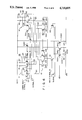
- FIG. 6 shows a logic operation circuit constituted in accordance with the circuits 10, 12 and 14. Note that in this circuit, transistors Q30 and Q31 are used instead of the transistor Q3 of the circuit 10, transistors Q40 and Q41 are used instead of the transistor Q4, transistors Q50 and Q51 are used instead of the transistor Q5, and transistors Q60 and Q61 are used instead of the transistor Q6.
- the constant current source CCS1 is constituted by an npn transistor Q100 whose collector is connected to the emitters of the transistors Ql and Q2, whose emitter is grounded through a resistor R5, and whose base is connected to receive a voltage VB. Furthermore, the circuit shown in FIG.
- the transistors Q1, Q30, Q31, Q8, Q13 and Q103 are turned on. Therefore, an operating current flows through the transistors Q103 and Q101, and a current flows through the transistors Q8, Q30, Q1 and Q100 and through the transistors Q13, Q31, Q1 and Q100.
- the sum signal QS of "0" level is generated from the circuit 12, and the carry output signal of "1" level is generated from the circuit 14.
Landscapes
- Physics & Mathematics (AREA)
- General Physics & Mathematics (AREA)
- Engineering & Computer Science (AREA)
- Computational Mathematics (AREA)
- Mathematical Analysis (AREA)
- Pure & Applied Mathematics (AREA)
- Theoretical Computer Science (AREA)
- Computing Systems (AREA)
- Mathematical Optimization (AREA)
- General Engineering & Computer Science (AREA)
- Logic Circuits (AREA)
Applications Claiming Priority (2)
| Application Number | Priority Date | Filing Date | Title |
|---|---|---|---|
| JP59105116A JPS60247733A (ja) | 1984-05-24 | 1984-05-24 | 論理演算回路 |
| JP59-105116 | 1984-05-24 |
Publications (1)
| Publication Number | Publication Date |
|---|---|
| US4718035A true US4718035A (en) | 1988-01-05 |
Family
ID=14398852
Family Applications (1)
| Application Number | Title | Priority Date | Filing Date |
|---|---|---|---|
| US06/734,078 Expired - Lifetime US4718035A (en) | 1984-05-24 | 1985-05-15 | Logic operation circuit having an exclusive-OR circuit |
Country Status (3)
| Country | Link |
|---|---|
| US (1) | US4718035A (de) |
| EP (1) | EP0173799A3 (de) |
| JP (1) | JPS60247733A (de) |
Cited By (12)
| Publication number | Priority date | Publication date | Assignee | Title |
|---|---|---|---|---|
| US4831579A (en) * | 1984-05-24 | 1989-05-16 | Kabushiki Kaisha Toshiba | Full adder circuit having an exclusive-OR circuit |
| US4831578A (en) * | 1985-11-25 | 1989-05-16 | Harris Semiconductor (Patents) Inc. | Binary adder |
| US4916653A (en) * | 1987-08-28 | 1990-04-10 | Hitachi, Ltd. | Adder using multi-state logic |
| US4918640A (en) * | 1988-02-05 | 1990-04-17 | Siemens Aktiengesellschaft | Adder cell having a sum part and a carry part |
| WO1991013392A2 (en) * | 1990-02-12 | 1991-09-05 | Micron Technology, Inc. | Easily configurable fully differential fast logic circuit |
| US5122687A (en) * | 1988-08-27 | 1992-06-16 | Ant Nachrichtentechnik Gmbh | Symmetrical exclusive-or gate, and modification thereof to provide an analog multiplier |
| US5175703A (en) * | 1991-04-29 | 1992-12-29 | Motorola, Inc. | High speed full adder and method |
| US5192882A (en) * | 1989-05-30 | 1993-03-09 | Board Of Regents, The University Of Texas System | Synchronization circuit for parallel processing |
| US5491653A (en) * | 1994-10-06 | 1996-02-13 | International Business Machines Corporation | Differential carry-save adder and multiplier |
| US5736868A (en) * | 1995-11-28 | 1998-04-07 | Korea Institute Of Science And Technology | Exclusive OR/NOR gate circuit |
| US20070040585A1 (en) * | 2005-08-22 | 2007-02-22 | Micron Technology, Inc. | High speed, low power CMOS logic gate |
| US7557614B1 (en) | 2008-07-15 | 2009-07-07 | International Business Machines Corporation | Topology for a n-way XOR/XNOR circuit |
Families Citing this family (1)
| Publication number | Priority date | Publication date | Assignee | Title |
|---|---|---|---|---|
| US4718034A (en) * | 1984-11-08 | 1988-01-05 | Data General Corporation | Carry-save propagate adder |
Citations (11)
| Publication number | Priority date | Publication date | Assignee | Title |
|---|---|---|---|---|
| US3519810A (en) * | 1967-02-14 | 1970-07-07 | Motorola Inc | Logic element (full adder) using transistor tree-like configuration |
| JPS4532992Y1 (de) * | 1970-07-09 | 1970-12-16 | ||
| US3590230A (en) * | 1969-04-03 | 1971-06-29 | Bell Telephone Labor Inc | Full adder employing exclusive-nor circuitry |
| US3612847A (en) * | 1964-04-03 | 1971-10-12 | Saint Gobain | Electrical apparatus and method for adding binary numbers |
| US4215418A (en) * | 1978-06-30 | 1980-07-29 | Trw Inc. | Integrated digital multiplier circuit using current mode logic |
| US4408134A (en) * | 1981-01-19 | 1983-10-04 | Advanced Micro Devices, Inc. | Unitary exclusive or-and logic circuit |
| JPS58211252A (ja) * | 1982-06-03 | 1983-12-08 | Toshiba Corp | 全加算器 |
| US4547863A (en) * | 1982-06-09 | 1985-10-15 | International Standard Electric Corporation | Integrated circuit three-input binary adder cell with high-speed sum propagation |
| US4605871A (en) * | 1984-03-12 | 1986-08-12 | Amdahl Corporation | Inverter function logic gate |
| US4621338A (en) * | 1983-04-15 | 1986-11-04 | Itt Industries, Inc. | CMOS adder using exclusive OR and/or exclusive-NOR gates |
| US4633104A (en) * | 1983-09-15 | 1986-12-30 | Ferranti Plc | Bipolar transistor logic circuits |
Family Cites Families (3)
| Publication number | Priority date | Publication date | Assignee | Title |
|---|---|---|---|---|
| JPS5331927A (en) * | 1976-09-06 | 1978-03-25 | Nippon Telegr & Teleph Corp <Ntt> | Logical sum circuit |
| JPS5360129A (en) * | 1976-11-10 | 1978-05-30 | Nippon Telegr & Teleph Corp <Ntt> | Full adder circuit |
| JPS58114237A (ja) * | 1981-12-28 | 1983-07-07 | Matsushita Electric Ind Co Ltd | 全加算器 |
-
1984
- 1984-05-24 JP JP59105116A patent/JPS60247733A/ja active Pending
-
1985
- 1985-05-15 US US06/734,078 patent/US4718035A/en not_active Expired - Lifetime
- 1985-05-24 EP EP85106409A patent/EP0173799A3/de not_active Withdrawn
Patent Citations (12)
| Publication number | Priority date | Publication date | Assignee | Title |
|---|---|---|---|---|
| US3612847A (en) * | 1964-04-03 | 1971-10-12 | Saint Gobain | Electrical apparatus and method for adding binary numbers |
| US3519810A (en) * | 1967-02-14 | 1970-07-07 | Motorola Inc | Logic element (full adder) using transistor tree-like configuration |
| US3590230A (en) * | 1969-04-03 | 1971-06-29 | Bell Telephone Labor Inc | Full adder employing exclusive-nor circuitry |
| JPS4532992Y1 (de) * | 1970-07-09 | 1970-12-16 | ||
| US4215418A (en) * | 1978-06-30 | 1980-07-29 | Trw Inc. | Integrated digital multiplier circuit using current mode logic |
| US4408134A (en) * | 1981-01-19 | 1983-10-04 | Advanced Micro Devices, Inc. | Unitary exclusive or-and logic circuit |
| JPS58211252A (ja) * | 1982-06-03 | 1983-12-08 | Toshiba Corp | 全加算器 |
| US4564921A (en) * | 1982-06-03 | 1986-01-14 | Tokyo Shibaura Kenki Kabushiki Kaisha | Full adder |
| US4547863A (en) * | 1982-06-09 | 1985-10-15 | International Standard Electric Corporation | Integrated circuit three-input binary adder cell with high-speed sum propagation |
| US4621338A (en) * | 1983-04-15 | 1986-11-04 | Itt Industries, Inc. | CMOS adder using exclusive OR and/or exclusive-NOR gates |
| US4633104A (en) * | 1983-09-15 | 1986-12-30 | Ferranti Plc | Bipolar transistor logic circuits |
| US4605871A (en) * | 1984-03-12 | 1986-08-12 | Amdahl Corporation | Inverter function logic gate |
Non-Patent Citations (1)
| Title |
|---|
| Application of Digital Signal Processing; The Institute of Electronics and Communications Engineers of Japan. * |
Cited By (14)
| Publication number | Priority date | Publication date | Assignee | Title |
|---|---|---|---|---|
| US4831579A (en) * | 1984-05-24 | 1989-05-16 | Kabushiki Kaisha Toshiba | Full adder circuit having an exclusive-OR circuit |
| US4831578A (en) * | 1985-11-25 | 1989-05-16 | Harris Semiconductor (Patents) Inc. | Binary adder |
| US4916653A (en) * | 1987-08-28 | 1990-04-10 | Hitachi, Ltd. | Adder using multi-state logic |
| US4918640A (en) * | 1988-02-05 | 1990-04-17 | Siemens Aktiengesellschaft | Adder cell having a sum part and a carry part |
| US5122687A (en) * | 1988-08-27 | 1992-06-16 | Ant Nachrichtentechnik Gmbh | Symmetrical exclusive-or gate, and modification thereof to provide an analog multiplier |
| US5192882A (en) * | 1989-05-30 | 1993-03-09 | Board Of Regents, The University Of Texas System | Synchronization circuit for parallel processing |
| WO1991013392A3 (en) * | 1990-02-12 | 1991-10-31 | Micron Technology Inc | Easily configurable fully differential fast logic circuit |
| WO1991013392A2 (en) * | 1990-02-12 | 1991-09-05 | Micron Technology, Inc. | Easily configurable fully differential fast logic circuit |
| US5175703A (en) * | 1991-04-29 | 1992-12-29 | Motorola, Inc. | High speed full adder and method |
| US5491653A (en) * | 1994-10-06 | 1996-02-13 | International Business Machines Corporation | Differential carry-save adder and multiplier |
| US5736868A (en) * | 1995-11-28 | 1998-04-07 | Korea Institute Of Science And Technology | Exclusive OR/NOR gate circuit |
| US20070040585A1 (en) * | 2005-08-22 | 2007-02-22 | Micron Technology, Inc. | High speed, low power CMOS logic gate |
| US7285986B2 (en) | 2005-08-22 | 2007-10-23 | Micron Technology, Inc. | High speed, low power CMOS logic gate |
| US7557614B1 (en) | 2008-07-15 | 2009-07-07 | International Business Machines Corporation | Topology for a n-way XOR/XNOR circuit |
Also Published As
| Publication number | Publication date |
|---|---|
| EP0173799A2 (de) | 1986-03-12 |
| EP0173799A3 (de) | 1989-04-05 |
| JPS60247733A (ja) | 1985-12-07 |
Similar Documents
| Publication | Publication Date | Title |
|---|---|---|
| US4718035A (en) | Logic operation circuit having an exclusive-OR circuit | |
| US4831579A (en) | Full adder circuit having an exclusive-OR circuit | |
| US5528171A (en) | ECL-to-CMOS signal level converter | |
| US5986501A (en) | Low voltage, beta immune variable gain amplifier with high supply voltage rejection | |
| US5315176A (en) | Differential ECL circuit | |
| US5438280A (en) | Input circuit receiving input signal of TTL level | |
| JPH07141452A (ja) | 乗算回路 | |
| JP3256664B2 (ja) | レベル変換回路 | |
| US4654602A (en) | Current mirror circuit | |
| US3976896A (en) | Reference voltage sources | |
| US5170079A (en) | Collector dot and circuit with latched comparator | |
| JP2546004B2 (ja) | レベル変換回路 | |
| JP2942589B2 (ja) | 半導体集積回路 | |
| US5684414A (en) | Voltage level interface circuit with separate reference signal input and folded cascode structure | |
| US4007384A (en) | Noninverting current-mode logic gate | |
| US4510486A (en) | Digital-to-analog converter | |
| JP2798010B2 (ja) | 差動デコード回路 | |
| US5796243A (en) | Current multiplier/divider circuit | |
| JP2829361B2 (ja) | いくつかの入力電圧の中の極値電圧を供給するための回路 | |
| US5869994A (en) | Level converter circuit converting input level into ECL-level against variation in power supply voltage | |
| US5656927A (en) | Circuit arrangement for generating a bias potential | |
| JPS617709A (ja) | 電流変換回路 | |
| JP2797620B2 (ja) | 比較回路 | |
| JP3039174B2 (ja) | スイッチ回路 | |
| JP3369878B2 (ja) | エミッタ結合トランジスタ対制御回路 |
Legal Events
| Date | Code | Title | Description |
|---|---|---|---|
| AS | Assignment |
Owner name: KABUSHIKI KAISHA TOSHIBA, 72 HORIKAWA-CHO, SAIWAI- Free format text: ASSIGNMENT OF ASSIGNORS INTEREST.;ASSIGNORS:HARA, HIROYUKI;SUGIMOTO, YASUHIRO;REEL/FRAME:004410/0990 Effective date: 19850424 |
|
| STCF | Information on status: patent grant |
Free format text: PATENTED CASE |
|
| FEPP | Fee payment procedure |
Free format text: PAYOR NUMBER ASSIGNED (ORIGINAL EVENT CODE: ASPN); ENTITY STATUS OF PATENT OWNER: LARGE ENTITY |
|
| FPAY | Fee payment |
Year of fee payment: 4 |
|
| FPAY | Fee payment |
Year of fee payment: 8 |
|
| FPAY | Fee payment |
Year of fee payment: 12 |