KR20120090787A - Semiconductor memory device - Google Patents
Semiconductor memory device Download PDFInfo
- Publication number
- KR20120090787A KR20120090787A KR1020120003743A KR20120003743A KR20120090787A KR 20120090787 A KR20120090787 A KR 20120090787A KR 1020120003743 A KR1020120003743 A KR 1020120003743A KR 20120003743 A KR20120003743 A KR 20120003743A KR 20120090787 A KR20120090787 A KR 20120090787A
- Authority
- KR
- South Korea
- Prior art keywords
- wiring
- memory cell
- layer
- transistor
- semiconductor
- Prior art date
- Legal status (The legal status is an assumption and is not a legal conclusion. Google has not performed a legal analysis and makes no representation as to the accuracy of the status listed.)
- Ceased
Links
Images


Classifications
-
- H—ELECTRICITY
- H10—SEMICONDUCTOR DEVICES; ELECTRIC SOLID-STATE DEVICES NOT OTHERWISE PROVIDED FOR
- H10D—INORGANIC ELECTRIC SEMICONDUCTOR DEVICES
- H10D88/00—Three-dimensional [3D] integrated devices
-
- H—ELECTRICITY
- H10—SEMICONDUCTOR DEVICES; ELECTRIC SOLID-STATE DEVICES NOT OTHERWISE PROVIDED FOR
- H10B—ELECTRONIC MEMORY DEVICES
- H10B12/00—Dynamic random access memory [DRAM] devices
- H10B12/30—DRAM devices comprising one-transistor - one-capacitor [1T-1C] memory cells
- H10B12/31—DRAM devices comprising one-transistor - one-capacitor [1T-1C] memory cells having a storage electrode stacked over the transistor
-
- G—PHYSICS
- G11—INFORMATION STORAGE
- G11C—STATIC STORES
- G11C11/00—Digital stores characterised by the use of particular electric or magnetic storage elements; Storage elements therefor
- G11C11/21—Digital stores characterised by the use of particular electric or magnetic storage elements; Storage elements therefor using electric elements
- G11C11/34—Digital stores characterised by the use of particular electric or magnetic storage elements; Storage elements therefor using electric elements using semiconductor devices
- G11C11/40—Digital stores characterised by the use of particular electric or magnetic storage elements; Storage elements therefor using electric elements using semiconductor devices using transistors
- G11C11/401—Digital stores characterised by the use of particular electric or magnetic storage elements; Storage elements therefor using electric elements using semiconductor devices using transistors forming cells needing refreshing or charge regeneration, i.e. dynamic cells
- G11C11/4063—Auxiliary circuits, e.g. for addressing, decoding, driving, writing, sensing or timing
- G11C11/407—Auxiliary circuits, e.g. for addressing, decoding, driving, writing, sensing or timing for memory cells of the field-effect type
- G11C11/408—Address circuits
- G11C11/4085—Word line control circuits, e.g. word line drivers, - boosters, - pull-up, - pull-down, - precharge
-
- G—PHYSICS
- G11—INFORMATION STORAGE
- G11C—STATIC STORES
- G11C5/00—Details of stores covered by group G11C11/00
- G11C5/06—Arrangements for interconnecting storage elements electrically, e.g. by wiring
- G11C5/10—Arrangements for interconnecting storage elements electrically, e.g. by wiring for interconnecting capacitors
-
- H—ELECTRICITY
- H10—SEMICONDUCTOR DEVICES; ELECTRIC SOLID-STATE DEVICES NOT OTHERWISE PROVIDED FOR
- H10B—ELECTRONIC MEMORY DEVICES
- H10B12/00—Dynamic random access memory [DRAM] devices
- H10B12/01—Manufacture or treatment
- H10B12/02—Manufacture or treatment for one transistor one-capacitor [1T-1C] memory cells
- H10B12/05—Making the transistor
-
- H—ELECTRICITY
- H10—SEMICONDUCTOR DEVICES; ELECTRIC SOLID-STATE DEVICES NOT OTHERWISE PROVIDED FOR
- H10B—ELECTRONIC MEMORY DEVICES
- H10B12/00—Dynamic random access memory [DRAM] devices
- H10B12/30—DRAM devices comprising one-transistor - one-capacitor [1T-1C] memory cells
-
- H—ELECTRICITY
- H10—SEMICONDUCTOR DEVICES; ELECTRIC SOLID-STATE DEVICES NOT OTHERWISE PROVIDED FOR
- H10B—ELECTRONIC MEMORY DEVICES
- H10B12/00—Dynamic random access memory [DRAM] devices
- H10B12/30—DRAM devices comprising one-transistor - one-capacitor [1T-1C] memory cells
- H10B12/48—Data lines or contacts therefor
-
- H—ELECTRICITY
- H10—SEMICONDUCTOR DEVICES; ELECTRIC SOLID-STATE DEVICES NOT OTHERWISE PROVIDED FOR
- H10B—ELECTRONIC MEMORY DEVICES
- H10B12/00—Dynamic random access memory [DRAM] devices
- H10B12/50—Peripheral circuit region structures
-
- H—ELECTRICITY
- H10—SEMICONDUCTOR DEVICES; ELECTRIC SOLID-STATE DEVICES NOT OTHERWISE PROVIDED FOR
- H10D—INORGANIC ELECTRIC SEMICONDUCTOR DEVICES
- H10D1/00—Resistors, capacitors or inductors
- H10D1/01—Manufacture or treatment
- H10D1/041—Manufacture or treatment of capacitors having no potential barriers
- H10D1/042—Manufacture or treatment of capacitors having no potential barriers using deposition processes to form electrode extensions
-
- H—ELECTRICITY
- H10—SEMICONDUCTOR DEVICES; ELECTRIC SOLID-STATE DEVICES NOT OTHERWISE PROVIDED FOR
- H10D—INORGANIC ELECTRIC SEMICONDUCTOR DEVICES
- H10D1/00—Resistors, capacitors or inductors
- H10D1/60—Capacitors
- H10D1/68—Capacitors having no potential barriers
- H10D1/692—Electrodes
- H10D1/711—Electrodes having non-planar surfaces, e.g. formed by texturisation
- H10D1/716—Electrodes having non-planar surfaces, e.g. formed by texturisation having vertical extensions
-
- H—ELECTRICITY
- H10—SEMICONDUCTOR DEVICES; ELECTRIC SOLID-STATE DEVICES NOT OTHERWISE PROVIDED FOR
- H10D—INORGANIC ELECTRIC SEMICONDUCTOR DEVICES
- H10D30/00—Field-effect transistors [FET]
- H10D30/60—Insulated-gate field-effect transistors [IGFET]
- H10D30/67—Thin-film transistors [TFT]
- H10D30/674—Thin-film transistors [TFT] characterised by the active materials
- H10D30/6755—Oxide semiconductors, e.g. zinc oxide, copper aluminium oxide or cadmium stannate
-
- H—ELECTRICITY
- H10—SEMICONDUCTOR DEVICES; ELECTRIC SOLID-STATE DEVICES NOT OTHERWISE PROVIDED FOR
- H10D—INORGANIC ELECTRIC SEMICONDUCTOR DEVICES
- H10D86/00—Integrated devices formed in or on insulating or conducting substrates, e.g. formed in silicon-on-insulator [SOI] substrates or on stainless steel or glass substrates
- H10D86/01—Manufacture or treatment
-
- H—ELECTRICITY
- H10—SEMICONDUCTOR DEVICES; ELECTRIC SOLID-STATE DEVICES NOT OTHERWISE PROVIDED FOR
- H10D—INORGANIC ELECTRIC SEMICONDUCTOR DEVICES
- H10D86/00—Integrated devices formed in or on insulating or conducting substrates, e.g. formed in silicon-on-insulator [SOI] substrates or on stainless steel or glass substrates
- H10D86/40—Integrated devices formed in or on insulating or conducting substrates, e.g. formed in silicon-on-insulator [SOI] substrates or on stainless steel or glass substrates characterised by multiple TFTs
- H10D86/441—Interconnections, e.g. scanning lines
-
- H—ELECTRICITY
- H10—SEMICONDUCTOR DEVICES; ELECTRIC SOLID-STATE DEVICES NOT OTHERWISE PROVIDED FOR
- H10D—INORGANIC ELECTRIC SEMICONDUCTOR DEVICES
- H10D86/00—Integrated devices formed in or on insulating or conducting substrates, e.g. formed in silicon-on-insulator [SOI] substrates or on stainless steel or glass substrates
- H10D86/40—Integrated devices formed in or on insulating or conducting substrates, e.g. formed in silicon-on-insulator [SOI] substrates or on stainless steel or glass substrates characterised by multiple TFTs
- H10D86/60—Integrated devices formed in or on insulating or conducting substrates, e.g. formed in silicon-on-insulator [SOI] substrates or on stainless steel or glass substrates characterised by multiple TFTs wherein the TFTs are in active matrices
-
- H—ELECTRICITY
- H10—SEMICONDUCTOR DEVICES; ELECTRIC SOLID-STATE DEVICES NOT OTHERWISE PROVIDED FOR
- H10D—INORGANIC ELECTRIC SEMICONDUCTOR DEVICES
- H10D87/00—Integrated devices comprising both bulk components and either SOI or SOS components on the same substrate
-
- H10W20/43—
-
- H10W20/4421—
Landscapes
- Engineering & Computer Science (AREA)
- Microelectronics & Electronic Packaging (AREA)
- Computer Hardware Design (AREA)
- Manufacturing & Machinery (AREA)
- Power Engineering (AREA)
- Physics & Mathematics (AREA)
- Semiconductor Memories (AREA)
- General Physics & Mathematics (AREA)
- Condensed Matter Physics & Semiconductors (AREA)
- Thin Film Transistor (AREA)
- Geometry (AREA)
- Metal-Oxide And Bipolar Metal-Oxide Semiconductor Integrated Circuits (AREA)
- Dram (AREA)
- Internal Circuitry In Semiconductor Integrated Circuit Devices (AREA)
- Electrodes Of Semiconductors (AREA)
Abstract
본 발명은, DRAM의 대기억 용량화를 더 도모하는 것이다.
반도체 기억 장치가, 단결정 반도체 재료를 포함하는 기판의 일부를 갖는 구동 회로와, 상기 구동 회로 위에 형성되는 다층 배선층과, 상기 다층 배선층 위에 형성되는 메모리 셀 어레이층을 갖는다. 즉, 상기 반도체 기억 장치에 있어서는, 구동 회로와 메모리 셀 어레이가 중첩하여 형성된다. 따라서, 단결정 반도체 재료를 포함하는 기판에 구동 회로 및 메모리 셀 어레이를 동일 평면에 형성하는 경우와 비교하여, 상기 반도체 기억 장치의 집적도를 높일 수 있다.The present invention further aims to increase the storage capacity of DRAM.
The semiconductor memory device includes a drive circuit having a portion of a substrate containing a single crystal semiconductor material, a multilayer wiring layer formed on the drive circuit, and a memory cell array layer formed on the multilayer wiring layer. That is, in the semiconductor memory device, the driver circuit and the memory cell array are formed to overlap each other. Therefore, compared with the case where the drive circuit and the memory cell array are formed on the same plane on the substrate containing the single crystal semiconductor material, the integration degree of the semiconductor memory device can be increased.
Description
본 발명은, 반도체 기억 장치에 관한 것이다. 특히, 산화물 반도체를 사용하여 채널 영역이 형성되는 트랜지스터가 형성된 메모리 셀을 갖는 반도체 기억 장치에 관한 것이다.The present invention relates to a semiconductor memory device. And more particularly to a semiconductor memory device having a memory cell in which a transistor in which a channel region is formed using an oxide semiconductor is formed.
근년에 들어, 트랜지스터의 구성 재료로서, 높은 이동도와 균일한 소자 특성을 겸비한 산화물 반도체라고 불리는, 반도체 특성을 나타내는 금속 산화물이 주목되고 있다. 금속 산화물은 다양한 용도에 사용되고 있다. 예를 들어, 산화인듐은 액정 표시 장치에 있어서 화소 전극의 재료로서 사용되고 있다. 반도체 특성을 나타내는 금속 산화물로서는, 예를 들어 산화텅스텐, 산화주석, 산화인듐, 산화아연 등이 있고, 이와 같은 반도체 특성을 나타내는 금속 산화물을 채널 영역에 사용하는 트랜지스터가 이미 알려져 있다(특허 문헌 1 및 특허 문헌 2).In recent years, as a constituent material of a transistor, the metal oxide which shows semiconductor characteristics called an oxide semiconductor which has high mobility and uniform element characteristics is attracting attention. Metal oxides are used in various applications. For example, indium oxide is used as a material of a pixel electrode in a liquid crystal display device. Examples of the metal oxide exhibiting semiconductor characteristics include tungsten oxide, tin oxide, indium oxide, zinc oxide, and the like, and transistors using a metal oxide exhibiting such semiconductor characteristics in a channel region have been known (Patent Documents 1 and 2). Patent Document 2).
그런데, 반도체 기억 장치에는, 휘발성 메모리로 분류되는 DRAM, SRAM, 불휘발성 메모리로 분류되는 마스크 ROM, EPROM, EEPROM, 플래시 메모리, 강유전체 메모리 등이 있으며, 단결정 반도체 기판을 사용하여 형성된 이들 메모리의 대부분은 이미 실용화되어 있다. 상기 기억 장치 중에서도 DRAM은 트랜지스터와 커패시터로 메모리 셀을 구성하는 단순한 구조를 갖고, SRAM 등의 다른 기억 장치와 비교하여 메모리 셀을 구성하기 위한 반도체 소자가 적다. 따라서, 다른 기억 장치와 비교하여 단위 면적당의 기억 용량을 높일 수 있고, 저비용화를 실현할 수 있다.By the way, semiconductor memory devices include DRAMs, SRAMs, mask ROMs, EPROMs, EEPROMs, flash memories, ferroelectric memories, and the like, which are classified as volatile memories, and most of these memories formed by using single crystal semiconductor substrates. It is already put to practical use. Among the above-mentioned memory devices, DRAMs have a simple structure of constituting memory cells with transistors and capacitors, and there are fewer semiconductor elements for constituting memory cells as compared with other memory devices such as SRAM. Therefore, compared with other memory devices, the storage capacity per unit area can be increased, and the cost can be realized.
상술한 바와 같이, DRAM은 대기억용량화에 적합하지만, 칩 크기가 증대하는 것을 억제하면서 집적도가 더 높은 집적 회로를 실현하기 위하여는, 다른 기억 장치와 마찬가지로 단위 면적당의 기억 용량을 높일 필요가 있다. 그 목적을 달성하기 위하여는, 전하를 유지하기 위하여 각 메모리 셀에 설치된 커패시터의 면적을 작게 하여, 각 메모리 셀의 면적을 축소화할 수밖에 없다.As described above, DRAM is suitable for increasing the storage capacity, but in order to realize an integrated circuit having a higher integration while suppressing an increase in chip size, it is necessary to increase the storage capacity per unit area like other storage devices. . In order to achieve the object, the area of the capacitors provided in each memory cell is kept small in order to maintain the electric charge, thereby reducing the area of each memory cell.
예를 들어, 각 메모리 셀의 면적의 축소화를 목적으로 하여, 반도체 기판에 깊은 홈을 형성하여 상기 홈에 커패시터를 형성하는 기술(즉, 트렌치형 커패시터) 또는 반도체 기판의 직상(直上) 방향으로 또는 대략 직상 방향으로 긴 커패시터를 형성하는 기술(즉, 스택형 커패시터) 등이 개발되고 있다. 구체적으로는 애스팩트비가 50 이상이 되는 커패시터가 개발되고 있다. 또한, 상기 반도체 기판 위에 계층화(階層化)된 복수의 배선층을 형성함으로써, 고집적화된 상기 반도체 기판에 형성되는 방대한 개수의 반도체 소자가 전기적으로 접속될 수 있게 하는 기술(즉, 다층 배선 기술) 등도 개발되고 있다.For example, for the purpose of reducing the area of each memory cell, a technique for forming a capacitor in the groove by forming a deep groove in the semiconductor substrate (i.e., a trench type capacitor) or in a direct direction of the semiconductor substrate or Techniques for forming long capacitors in a substantially straight direction (ie, stacked capacitors) have been developed. Specifically, capacitors having an aspect ratio of 50 or more have been developed. In addition, by forming a plurality of layered wiring layers on the semiconductor substrate, a technology (ie, a multilayer wiring technique) or the like that enables a large number of semiconductor elements formed on the highly integrated semiconductor substrate to be electrically connected to each other is also developed. It is becoming.
그래서, 본 발명의 일 형태에 있어서는, DRAM의 대기억용량화를 더 도모하는 것을 목적의 하나로 한다.Thus, one embodiment of the present invention aims to further increase the atmospheric storage capacity of DRAM.
본 발명의 일 형태인 반도체 기억 장치는, 단결정 반도체 재료를 포함하는 기판의 일부를 갖는 구동 회로 위에 다층 배선층을 개재(介在)하여 메모리 셀 어레이를 형성하는 것을 요지로 한다.A semiconductor memory device of one embodiment of the present invention has a main purpose of forming a memory cell array with a multilayer wiring layer interposed on a drive circuit having a part of a substrate containing a single crystal semiconductor material.
구체적으로는, 본 발명의 일 형태는, 단결정 반도체 기판의 일부를 갖는 구동 회로와, 구동 회로 위에 형성되고 또 복수의 구리 또는 구리 합금을 포함하는 배선을 포함하는 다층 배선층과, 다층 배선층 위에 형성되고 또매트릭스 형상으로 배설된 복수의 메모리 셀을 포함하는 메모리 셀어레이층을 갖고, 구동 회로와 복수의 메모리 셀각각은 복수의 구리 또는 구리 합금을 포함하는 배선의 적어도 하나를 통하여 전기적으로 접속되고, 복수의 메모리 셀 각각은 산화물 반도체를 사용하여 채널 영역이 형성되는 트랜지스터와, 한쪽의 전극이 트랜지스터의 소스 및 드레인 중 한쪽에 전기적으로 접속되는 커패시터를 갖는 반도체 기억 장치이다.Specifically, one embodiment of the present invention is formed on a multi-layer wiring layer including a drive circuit having a portion of a single crystal semiconductor substrate, a wiring formed on the drive circuit and comprising a plurality of copper or copper alloys, and a multi-layer wiring layer. It further has a memory cell array layer including a plurality of memory cells arranged in a matrix shape, each of the driving circuit and the plurality of memory cells are electrically connected through at least one of the wirings comprising a plurality of copper or copper alloy, Each of the memory cells is a semiconductor memory device having a transistor in which a channel region is formed using an oxide semiconductor, and a capacitor in which one electrode is electrically connected to one of a source and a drain of the transistor.
본 발명의 일 형태에 따른 반도체 기억 장치는, 단결정 반도체 재료를 포함하는 기판의 일부를 갖는 구동 회로와 메모리 셀 어레이를 중첩하여 형성할 수 있다. 따라서, 단결정 반도체 재료를 포함하는 기판에 구동 회로 및 메모리 셀 어레이를 동일 평면에 형성하는 경우와 비교하여, 상기 반도체 기억 장치의 집적도를 높일 수 있다.The semiconductor memory device of one embodiment of the present invention can be formed by overlapping a drive circuit having a part of a substrate containing a single crystal semiconductor material and a memory cell array. Therefore, compared with the case where the drive circuit and the memory cell array are formed on the same plane on the substrate containing the single crystal semiconductor material, the degree of integration of the semiconductor memory device can be increased.
도 1은 반도체 기억 장치의 구성예를 도시한 도면.
도 2는 구동 회로가 갖는 트랜지스터의 구성예를 도시한 도면.
도 3a 내지 도 3h는 트랜지스터의 제작 방법의 일례를 도시한 도면.
도 4는 배선층의 구성예를 도시한 도면.
도 5a 내지 도 5h는 배선층의 제작 방법의 일례를 도시한 도면.
도 6은 메모리 셀의 구성예를 도시한 도면.
도 7a 내지 도 7h는 메모리 셀이 갖는 트랜지스터의 제작 방법의 일례를 도시한 도면.
도 8은 마이크로프로세서의 구성예를 도시한 블록도.
도 9a 내지 도 9c는 반도체 장치의 구체예를 도시한 도면.1 is a diagram showing a configuration example of a semiconductor memory device.
2 is a diagram showing an example of the configuration of a transistor included in a driving circuit;
3A to 3H illustrate an example of a method of fabricating a transistor.
4 is a diagram illustrating a configuration example of a wiring layer.
5A to 5H are views showing an example of a manufacturing method of a wiring layer.
6 is a diagram showing an example of the configuration of a memory cell;
7A to 7H illustrate an example of a method of manufacturing a transistor included in a memory cell.
8 is a block diagram showing a configuration example of a microprocessor.
9A to 9C show specific examples of the semiconductor device.
이하에서는, 본 발명의 실시형태에 대하여 도면을 사용하여 상세하게 설명한다. 다만, 본 발명은 이하의 설명에 한정되지 않고, 본 발명의 취지 및 그 범위에서 벗어남이 없이 그 형태 및 상세한 내용을 다양하게 변경할 수 있는 것은 당업자라면 용이하게 이해할 수 있다. 따라서, 본 발명은 이하에 기재하는 실시형태의 기재내용에 한정하여 해석되는 것이 아니다.EMBODIMENT OF THE INVENTION Hereinafter, embodiment of this invention is described in detail using drawing. However, the present invention is not limited to the following description, and it can be easily understood by those skilled in the art that various changes can be made in the form and details without departing from the spirit and scope of the present invention. Therefore, this invention is not interpreted limited to description of embodiment described below.
우선, 본 발명의 일 형태인 반도체 기억 장치의 구성예에 대하여 도 1 내지 도 7h를 참조하여 설명한다.First, a structural example of a semiconductor memory device of one embodiment of the present invention will be described with reference to FIGS. 1 to 7H.
<반도체 기억 장치의 구성예><Configuration example of semiconductor memory device>
도 1은, 반도체 기억 장치의 구성예를 도시한 도면이다. 도 1에 도시한 반도체 기억 장치는, 단결정 반도체 재료를 포함하는 기판(10)의 일부를 갖는 구동 회로(100)와, 구동 회로(100) 위에 형성된 다층 배선층(20)과, 다층 배선층(20) 위에 형성되고 또 매트릭스 형상으로 배설된 복수의 메모리 셀(300)을 포함하는 메모리 셀 어레이층(30)을 갖는다.1 is a diagram showing a configuration example of a semiconductor memory device. The semiconductor memory device shown in FIG. 1 includes a
구동 회로(100)는 단결정 반도체 재료를 포함하는 기판(10)을 사용하여 형성되는 복수의 반도체 소자에 의하여 구성된다. 그리고, 복수의 메모리 셀(300) 각각에 대하여 데이터의 기록 및 판독을 행하는 기능을 갖는다.The
다층 배선층(20)은, 각각에 복수의 배선(200)이 형성되는 평면을 갖는 복수의 배선층(20a), 배선층(20b)으로 구성된다. 그리고, 구동 회로(100)에 포함되는 반도체 소자끼리, 및 구동 회로(100)와 복수의 메모리 셀(300) 각각을 전기적으로 접속시키는 기능을 갖는다. 또한, 다층 배선층(20)에서는 복수의 배선(200)이 형성되는 평면이 계층화된다. 구체적으로는, 각각에 복수의 배선(200)이 매설된 복수의 절연층이 적층된다. 다만, 상이한 평면에 형성된 배선(200)끼리는 절연층을 관통하여 형성되는 콘택트 플러그(201)를 통하여 전기적으로 접속된다. 또한, 도 1에서는 2개의 배선층(20a), 배선층(20b)으로 구성되는 다층 배선층(20)을 예시하지만, 본 발명의 일 형태에 따른 다층 배선층(20)은 2층에 한정되지 않고, 3층 이상으로 구성할 수도 있다. 또한, 다층 배선층(20) 중 1층 이상을 사용하여 메모리 셀의 비트선을 형성하여도 좋다.The
복수의 메모리 셀(300) 각각은, 트랜지스터(301)와, 한쪽의 전극이 트랜지스터(301)의 소스 및 드레인 중 한쪽에 전기적으로 접속되는 커패시터(302)를 갖는다.Each of the plurality of
<구동 회로(100)의 구성예><Configuration example of
이하에 구동 회로(100)를 구성하는, 단결정 반도체 재료를 포함하는 기판(10)을 사용하여 형성되는 트랜지스터의 일례에 대하여 도 2를 참조하여 설명한다.An example of a transistor formed using the
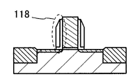
도 2에 도시한 트랜지스터(160)는 단결정 반도체 재료를 포함하는 기판(10)에 형성된 채널 영역(116)과, 채널 영역(116)을 사이에 끼우도록 형성된 한 쌍의 불순물 영역(114a, 114b) 및 한쌍의 고농도 불순물 영역(120a, 120b)(이들을 합쳐서 단순하게 "불순물 영역"이라고도 부름)과, 채널 영역(116) 위에 형성된 게이트 절연막(108)과, 게이트 절연막(108) 위에 형성된 게이트 전극(110)과, 불순물 영역(114a)과 전기적으로 접속되는 소스 전극(130a)과, 불순물 영역(114b)과 전기적으로 접속되는 드레인 전극(130b)을 갖는다.The
또한, 게이트 전극(110)의 측면에는 사이드 월 절연층(118)이 형성된다. 또한, 단결정 반도체 재료를 포함하는 기판(10)의 사이드 월 절연층(118)과 중첩하지 않는 영역에는 한 쌍의 고농도 불순물 영역(120a, 120b)이 존재하고, 한 쌍의 고농도 불순물 영역(120a, 120b) 위에는 한 쌍의 금속 화합물 영역(124a, 124b)이 존재한다. 또한, 기판(10) 위에는 트랜지스터(160)를 둘러싸도록 소자 분리 절연층(106)이 형성되고, 트랜지스터(160)를 둘러싸도록 층간 절연층(126) 및 층간 절연층(128)이 형성된다. 소스 전극(130a)은 층간 절연층(126) 및 층간 절연층(128)에 형성된 개구를 통하여 금속 화합물 영역(124a)과 전기적으로 접속되고, 드레인 전극(130b)은 층간 절연층(126) 및 층간 절연층(128)에 형성된 개구를 통하여 금속 화합물 영역(124b)과 전기적으로 접속된다. 즉, 소스 전극(130a)은 금속 화합물 영역(124a)을 통하여 고농도 불순물 영역(120a) 및 불순물 영역(114a)과 전기적으로 접속되고, 드레인 전극(130b)은 금속 화합물 영역(124b)을 통하여 고농도 불순물 영역(120b) 및 불순물 영역(114b)과 전기적으로 접속된다.In addition, a side
<트랜지스터의 제작 방법예><Example of transistor manufacturing method>
다음에, 트랜지스터(160)의 제작 방법의 일례에 대하여 도 3a 내지 도 3h를 참조하여 설명한다. 또한, 트랜지스터(160)는 이하의 방법에 한정되지 않고, 공지의 기술에 의하여 제작할 수 있다.Next, an example of a manufacturing method of the
우선, 단결정 반도체 재료를 포함하는 기판(10)을 준비한다(도 3a 참조). 단결정 반도체 재료를 포함하는 기판(10)으로서는, 실리콘, 탄화실리콘, 실리콘게르마늄, 또는 갈륨 비소 등의 단결정 반도체 기판, 및 이들 단결정층을 절연층 위에 형성한 SOI 기판 등을 적용할 수 있다. 또한, 일반적으로 「SOI 기판」은 절연 표면 위에 실리콘 반도체층이 형성된 구성의 기판을 말하지만, 본 명세서 등에 있어서는, 절연 표면 위에 실리콘 이외의 재료를 포함하는 반도체층이 형성된 구성의 기판도 포함하는 것으로 한다. 즉, 「SOI 기판」이 갖는 반도체층은 실리콘 반도체층에 한정되지 않는다. 또한, SOI 기판에는 유리 기판 등의 절연 기판 위에 절연층을 개재하여 반도체층이 형성된 구성도 포함되는 것으로 한다. 여기서는, 단결정 반도체 재료를 포함하는 기판(10)으로서 단결정 실리콘 기판을 사용하는 경우의 일례에 대하여 기재한다.First, the board |
기판(10) 위에는, 소자 분리 절연층을 형성하기 위한 마스크가 되는 보호층(102)을 형성한다(도 3a 참조). 보호층(102)으로서는, 예를 들어 산화실리콘이나 질화실리콘, 질화산화실리콘 등을 재료로 하는 절연층을 사용할 수 있다. 또한, 이 공정 전후에 있어서, 반도체 장치의 임계값 전압을 제어하기 위하여, n형의 도전성을 부여하는 불순물 원소나 p형의 도전성을 부여하는 불순물 원소를 기판(10)에 첨가하여도 좋다. 반도체가 실리콘인 경우, n형의 도전성을 부여하는 불순물로서는, 예를 들어, 인이나 비소 등을 사용할 수 있다. 또한, p형의 도전성을 부여하는 불순물로서는, 예를 들어 붕소, 알루미늄, 갈륨 등을 사용할 수 있다.On the board |
다음에, 상기 보호층(102)을 마스크로서 사용하여 에칭함으로써 보호층(102)으로 덮이지 않는 영역(노출되는 영역)의 기판(10)의 일부분을 제거한다. 이로써, 분리된 반도체 영역(104)이 형성된다(도 3b 참조). 상기 에칭에는 드라이 에칭을 사용하는 것이 적합하지만, 웨트 에칭을 사용하여도 좋다. 에칭 가스나 에칭액은 피에칭 재료에 따라 적절히 선택할 수 있다.Next, a portion of the
다음에, 반도체 영역(104)을 덮도록 절연층을 형성하고, 반도체 영역(104)에 중첩하는 영역의 절연층을 선택적으로 제거함으로써, 소자 분리 절연층(106)을 형성한다(도 3b 참조). 상기 절연층은 산화실리콘이나 질화실리콘, 질화산화실리콘 등을 사용하여 형성된다. 절연층의 제거 방법으로서는 CMP(Chemical Mechanical Polishing) 등의 연마 처리나 에칭 처리 등이 있는데, 그 중 어느 방법을 사용하여도 좋다. 또한, 반도체 영역(104)을 형성한 후, 또는 소자 분리 절연층(106)을 형성한 후에 상기 보호층(102)을 제거한다.Next, the insulating layer is formed so as to cover the
다음에, 반도체 영역(104) 위에 절연층을 형성하고, 상기 절연층 위에 도전 재료를 포함하는 층을 형성한다.Next, an insulating layer is formed over the
절연층은 나중의 게이트 절연막이 되는 것이며, CVD법이나 스퍼터링법 등을 사용하여 얻어지는 산화실리콘, 질화산화실리콘, 질화실리콘, 산화하프늄, 산화알루미늄, 산화탄탈 등을 포함하는 막의 단층 구조 또는 적층 구조로 하면 좋다. 그 외에 고밀도 플라즈마 처리나 열산화 처리에 의하여 반도체 영역(104)의 표면을 산화, 질화함으로써, 상기 절연층을 형성하여도 좋다. 고밀도 플라즈마 처리는, 예를 들어 He, Ar, Kr, Xe 등의 희 가스와, 산소, 산화질소, 암모니아, 질소 등과의 혼합 가스를 사용하여 행할 수 있다. 또한, 절연층의 유전율 및 두께는 제작하는 트랜지스터의 채널 길이에 따라 결정되는데, 예를 들어 1nm 이상 100nm 이하로 할 수 있다.The insulating layer serves as a later gate insulating film, and has a single layer structure or a laminated structure of a film containing silicon oxide, silicon nitride oxide, silicon nitride, hafnium oxide, aluminum oxide, tantalum oxide, or the like obtained by using a CVD method or a sputtering method. Do it. In addition, the insulating layer may be formed by oxidizing and nitriding the surface of the
도전 재료를 포함하는 층은 알루미늄이나, 구리, 티타늄, 탄탈, 텅스텐 등의 금속 재료를 사용하여 형성할 수 있다. 또한, 높은 도전성을 갖는 다결정 실리콘 등의 반도체 재료를 사용하여, 도전 재료를 포함하는 층을 형성하여도 좋다. 형성 방법도 특별히 한정되지 않고, 증착법, CVD법, 스퍼터링법, 스핀 코팅법 등의 각종 성막 방법을 사용할 수 있다. 또한, 여기에서는 도전 재료를 포함하는 층을 금속 재료를 사용하여 형성하는 경우의 일례에 대하여 나타내는 것으로 한다.The layer containing the conductive material can be formed using a metal material such as aluminum, copper, titanium, tantalum or tungsten. In addition, a layer containing a conductive material may be formed using a semiconductor material such as polycrystalline silicon having high conductivity. The formation method is not particularly limited, and various deposition methods such as a vapor deposition method, a CVD method, a sputtering method, and a spin coating method can be used. In addition, it shall show here about an example in the case of forming the layer containing an electrically-conductive material using a metal material.
그 후, 절연층 및 도전 재료를 포함하는 층을 선택적으로 에칭하여, 게이트 절연막(108), 게이트 전극(110)을 형성한다(도 3c 참조).Thereafter, the layer including the insulating layer and the conductive material is selectively etched to form the
다음에, 게이트 전극(110)을 덮는 절연층(112)을 형성한다(도 3c 참조). 그리고, 반도체 영역(104)에 붕소(B), 인(P), 비소(As) 등을 첨가하여, 얕은 접합 깊이의 한 쌍의 불순물 영역(114a, 114b)을 형성한다(도 3c 참조). 또한, 한 쌍의 불순물 영역(114a, 114b)을 형성함으로써, 반도체 영역(104)의 게이트 절연막(108) 하부에는 채널 영역(116)이 형성된다(도 3c 참조). 여기서, 첨가하는 불순물의 농도는 적절히 설정할 수 있지만, 반도체 소자가 고도로 미세화되는 경우에는, 그농도를 높게 하는 것이 바람직하다. 또한, 여기서는 절연층(112)을 형성한 후에 한 쌍의 불순물 영역(114a, 114b)을 형성하는 공정을 채용하지만, 한 쌍의 불순물 영역(114a, 114b)을 형성한 후에 절연층(112)을 형성하는 공정으로 하여도 좋다.Next, the insulating
다음에, 사이드 월 절연층(118)을 형성한다(도 3d 참조). 사이드 월 절연층(118)은 절연층(112)을 덮도록 절연층을 형성한 후에, 상기 절연층에 이방성이 높은 에칭 처리를 적용함으로써, 자기 정합적으로 형성할 수 있다. 또한, 이 때에 절연층(112)을 부분적으로 에칭하여, 게이트 전극(110)의 상면과 한 쌍의 불순물 영역(114a, 114b)의 상면을 일부 노출시키면 좋다.Next, the
다음에, 게이트 전극(110), 한 쌍의 불순물 영역(114a, 114b), 사이드 월 절연층(118) 등을 덮도록 절연층을 형성한다. 그리고, 한 쌍의 불순물 영역(114a, 114b)의 일부에 대하여 붕소(B), 인(P), 비소(As) 등을 첨가하여, 한 쌍의 고농도 불순물 영역(120a, 120b)을 형성한다(도 3e 참조). 필요에 따라, 한 쌍의 고농도 불순물 영역(120a, 120b) 외측에 반대의 도전형을 갖는 불순물을 주입하여, 소위 할로 영역(halo region)을 형성하여도 좋다. 그 후, 상기 절연층을 제거하고, 게이트 전극(110), 사이드 월 절연층(118), 한 쌍의 고농도 불순물 영역(120a, 120b) 등을 덮도록 금속층(122)을 형성한다(도 3e 참조). 금속층(122)은 진공 증착법이나 스퍼터링법, 스핀 코팅법 등의 각종 성막 방법을 사용하여 형성할 수 있다. 금속층(122)은, 반도체 영역(104)을 구성하는 반도체 재료와 반응하여 저저항의 금속 화합물이 되는 금속 재료를 사용하여 형성하는 것이 바람직하다. 이러한 금속 재료로서는, 예를 들어, 티타늄, 탄탈, 텅스텐, 니켈, 코발트, 백금 등이 있다.Next, an insulating layer is formed to cover the
다음에, 열 처리하여 금속층(122)과 반도체 재료를 반응시킨다. 이로써, 한 쌍의 고농도 불순물 영역(120a, 120b)에 접하는 한 쌍의 금속 화합물 영역(124a, 124b)이 형성된다(도 3f 참조). 또한, 게이트 전극(110)으로서 다결정 실리콘 등을 사용하는 경우에는 게이트 전극(110)의 금속층(122)과 접촉되는 부분에도 금속 화합물 영역이 형성된다.Next, heat treatment causes the
상기 열 처리로서는, 예를 들어, 플래시 램프를 조사하는 열 처리를 사용할 수 있다. 물론, 그 외의 열 처리 방법을 사용하여도 좋지만, 금속 화합물의 형성에 따른 화학 반응의 제어성을 향상시키기 위하여는, 극히 짧은 시간으로 열 처리를 실현할 수 있는 방법을 사용하는 것이 바람직하다. 또한, 상기 금속 화합물 영역은 금속 재료와 반도체 재료가 반응함으로써 형성되는 것이고, 충분히 도전성이 높여진 영역이다. 상기 금속 화합물 영역을 형성함으로써 전기 저항을 충분히 저감하고, 소자 특성을 향상시킬 수 있다. 또한, 한 쌍의 금속 화합물 영역(124a, 124b)을 형성한 후에는 금속층(122)을 제거한다.As said heat processing, the heat processing which irradiates a flash lamp can be used, for example. Of course, other heat treatment methods may be used, but in order to improve the controllability of the chemical reaction due to the formation of the metal compound, it is preferable to use a method capable of realizing the heat treatment in a very short time. The metal compound region is formed by reacting a metal material and a semiconductor material, and is a region having sufficiently high conductivity. By forming the said metal compound region, electric resistance can fully be reduced and element characteristic can be improved. After the pair of
다음에, 상술한 공정에 의하여 형성된 각 구성을 덮도록 층간 절연층(126), 층간 절연층(128)을 형성한다(도 3g 참조). 층간 절연층(126)이나 층간 절연층(128)은, 산화실리콘, 질화산화실리콘, 질화실리콘, 산화하프늄, 산화알루미늄, 산화탄탈 등의 무기 절연 재료를 사용하여 형성할 수 있다. 또한, 폴리이미드, 아크릴 등의 유기 절연 재료를 사용하여 형성할 수도 있다. 또한, 여기서는 층간 절연층(126)이나 층간 절연층(128)의 2층 구조로 구성하지만, 층간 절연층의 구성은 이것에 한정되지 않는다. 층간 절연층(128)의 형성 후에는 그의 표면을 CMP나 에칭 처리 등에 의하여 평탄화해 두는 것이 바람직하다.Next, the
그 후, 상기 층간 절연층에 한 쌍의 금속 화합물 영역(124a, 124b)에 도달하는 개구를 형성하고, 상기 개구에 소스 전극(130a), 드레인 전극(130b)을 형성한다(도 3h 참조). 소스 전극(130a) 및 드레인 전극(130b)은, 예를 들어 개구를 포함하는 영역에 PVD법이나 CVD법 등을 사용하여 도전층을 형성한 후, 에칭 처리나 CMP와 같은 방법을 사용하여 상기 도전층의 일부를 제거함으로써 형성할 수 있다.Thereafter, an opening reaching the pair of
또한, 소스 전극(130a) 및 드레인 전극(130b)을 형성할 때에는 그 표면이 평탄해지도록 가공하는 것이 바람직하다. 예를 들어, 개구를 포함하는 영역에 티타늄막이나 질화티타늄막을 얇게 형성한 후에, 개구에 매립되도록 텅스텐막을 형성하는 경우에는, 그 후의 CMP에 의하여 불필요한 텅스텐, 티타늄, 질화티타늄 등을 제거함과 함께, 그 표면의 평탄성을 향상시킬 수 있다. 이와 같이, 소스 전극(130a) 및 드레인 전극(130b)을 포함하는 표면을 평탄화함으로써, 후속 공정에 있어서 양호한 전극, 배선, 절연층, 반도체층 등을 형성할 수 있게 된다.In addition, when forming the
이로써, 단결정 반도체 재료를 포함하는 기판(10)을 사용한 트랜지스터(160)가 형성된다.As a result, the
<배선층(20a), 배선층(20b)의 구성예><Configuration example of
이하에서 배선층(20a), 배선층(20b)의 구성예에 대하여 도 4를 참조하여 설명한다.Hereinafter, the structural example of the
도 4에 도시한 배선층(20a)은 절연층(202)과, 절연층(202)의 개구부에 형성된 콘택트 플러그(201a), 콘택트 플러그(201b)와, 절연층(202) 위에 형성된 절연층(203)과, 절연층(203)의 개구부에 형성된 배선(200a), 배선(200b)을 갖는다. 또한, 배선층(20b)도 배선층(20a)과 같은 구성을 갖는다.The
또한, 절연층(202)은, 도 2에 도시한 트랜지스터(160) 위에 형성된다. 또한, 콘택트 플러그(201a)는 트랜지스터(160)가 갖는 소스 전극(130a) 및 배선(200a)에 접속되고, 콘택트 플러그(201b)는 트랜지스터(160)가 갖는 드레인 전극(130b) 및 배선(200b)에 접속된다.The insulating
<배선층(20a), 배선층(20b)의 제작 방법예><Example of manufacturing method of
다음에, 배선층(20a), 배선층(20b)의 제작 방법의 일례에 대하여 도 5a 내지 도 5h를 참조하여 설명한다.Next, an example of the manufacturing method of the
우선, 트랜지스터(160) 위에 절연층(202)을 형성한다(도 5a 참조, 또한, 도 5a 내지 도 5h에서는 트랜지스터(160)는 생략한다). 절연층(202)으로서는, 산화실리콘, 질화산화실리콘, 질화실리콘 등의 무기 절연 재료를 포함하는 막의 단층 구조, 또는 적층 구조 등을 적용할 수 있다. 예를 들어, 질화실리콘막 및 산화실리콘막의 적층을 절연층(202)으로서 적용할 수 있다. 특히, 그 후에 형성하는 배선(200a), 배선(200b)이 구리를 함유하는 경우에는, 구리가 트랜지스터(160)로 확산되지 않도록, 두께 5nm 내지 50nm의 질화실리콘막을 형성하고, 그 위에 필요한 두께의 산화실리콘막 등을 퇴적하는 적층 구조로 하는 것이 바람직하다. 절연층(202)의 제작 방법으로서는, CVD법 또는 스퍼터링법 등을 적용할 수 있다.First, an insulating
다음에, 절연층(202) 위에 포토리소그래피법 등을 사용하여 레지스트 마스크를 형성하고, 상기 레지스트 마스크를 사용하여 절연층(202)을 에칭함으로써, 개구부(204a), 개구부(204b)를 형성한다(도 5b 참조). 또한, 포토리소그래피법을 행하는 경우는 미리 절연층(202) 위에 반사 방지막을 형성해 두는 것이 바람직하다. 이로써, 포토리소그래피법의 노광 공정시에 있어서의, 트랜지스터(160)가 갖는 도전층(소스 전극(130a), 드레인 전극(130b) 등) 등에 의한 광 반사를 억제할 수 있다. 즉, 포토리소그래피법에 있어서의 해상도의 저하를 억제할 수 있다. 또한, 상기 반사 방지막의 재료는, 상기 레지스트의 재료 등에 따라 적절히 선택할 수 있다. 또한, 상기 에칭에는, 드라이 에칭을 사용하는 것이 적합하지만, 웨트 에칭을 사용하여도 좋다. 에칭 가스나 에칭액은 피에칭 재료에 따라 적절히 선택할 수 있다.Next, a resist mask is formed on the insulating
다음에, 적어도 개구부(204a), 개구부(204b)를 매몰시키도록 도전 재료를 포함하는 층(205)을 형성한다(도 5c 참조). 도전 재료를 포함하는 층(205)으로서는 알루미늄, 티타늄, 탄탈, 또는 텅스텐 등의 금속, 또는 이들의 질화물, 또는 이들의 합금 등을 포함하는 막을 적용할 수 있다. 또한, 도전 재료를 포함하는 층(205)로서 이들의 막의 적층 구조를 적용할 수도 있다. 예를 들어, 티타늄막, 질화티타늄막, 및 텅스텐막의 적층을 도전 재료를 포함하는 층(205)으로서 적용할 수 있다. 특히, 그 후에 형성하는 배선(200a), 배선(200b)이 구리를 함유하는 경우에는, 구리가 트랜지스터(160)로 확산되지 않도록, 도전 재료를 포함하는 층(205)이 두께 5nm 내지 50nm의 질화티타늄의 층을 갖는 것이 바람직하다. 도전 재료를 포함하는 층(205)의 제작 방법으로서는, CVD법 또는 스퍼터링법 등을 적용할 수 있다.Next, a
다음에, 적어도 절연층(202)의 상면이 노출되도록, 절연층(202) 위에 형성된 도전 재료를 포함하는 층(205)를 CMP에 의하여 제거한다(도 5d 참조). 이로써, 콘택트 플러그(201a), 콘택트 플러그(201b)가 형성된다.Next, the
다음에, 절연층(202) 및 콘택트 플러그(201a), 콘택트 플러그(201b) 위에 절연층(203)을 형성한다(도 5e 참조). 절연층(203)으로서는, 산화실리콘, 질화산화실리콘, 질화실리콘등의 무기 절연 재료를 포함하는 막, 또는 알킬실란 등의 유기 실란을 원료로 한 실리콘(silicone) 수지(즉, SiOC막) 등의 절연 재료의 단층 구조 또는 적층 구조 등을 적용할 수 있다. 예를 들어, SiOC막과 산화실리콘막의 적층을 절연층(203)으로서 적용할 수 있다. 또한, 절연층(203)의 제작 방법으로서는 CVD법, 스퍼터링법, 또는 스핀 코팅법을 적용할 수 있다.Next, an insulating
다음에, 절연층(203) 위에 포토리소그래피법 등을 사용하여 레지스트 마스크를 형성하고, 상기 레지스트 마스크를 사용하여 적어도 절연층(203)을 에칭함으로써, 홈(206a), 홈(206b)을 형성한다(도 5f 참조). 또한, 홈(206a), 홈(206b)은 적어도 절연층(203)을 관통하고, 콘택트 플러그(201a), 콘택트 플러그(201b)의 상면이 노출되도록 한다. 예를 들어, 처리 시간을 제어함으로써, 홈(206a), 홈(206b)이 원하는 형상으로 되도록 제어한다. 또한, 포토리소그래피법을 행하는 경우는 상술한 바와 같이 미리 절연층(203) 위에 반사 방지막을 형성해 두는 것이 바람직하다. 또한, 상기 에칭에는 드라이 에칭(특히, 반응성 이온 에칭(Reactive Ion Etching))을 사용하는 것이 바람직하다.Next, a resist mask is formed on the insulating
다음에, 적어도 홈(206a), 홈(206b)을 매몰시키도록 도전 재료를 포함하는 층(207)을 형성한다(도 5g 참조). 도전 재료를 포함하는 층(207)으로서는 구리, 알루미늄, 티타늄, 탄탈, 또는 텅스텐 등의 금속, 또는 이들의 질화물, 또는 이들의 합금 등을 포함하는 막을 적용할 수도 있다. 또한, 도전 재료를 포함하는 층(207)으로서, 이들의 막의 적층 구조를 적용할 수도 있다. 예를 들어, 질화탄탈막과 구리막의 적층을 도전 재료를 포함하는 층(207)으로서 적용할 수 있다. 또한, 도전 재료를 포함하는 층(207)의 제작 방법으로서는, CVD법 또는 스퍼터링법, 또는 이들의 방법에 의하여 시드층을 형성한 후에 전해 도금을 행하는 방법 등을 적용할 수 있다.Next, a layer 207 including a conductive material is formed to bury at least the
또한, 도전 재료를 포함하는 층(207)으로서는 구리 또는 구리 합금을 포함하는 막을 포함하는 배선을 적용하는 것이 바람직하다. 이로써, 배선 저항을 저감할 수 있다. 예를 들어, 두께 5nm 내지 50nm의 질화탄탈층을 CVD법에 의하여 형성하고, 두께 5nm 내지 50nm의 제1 구리층을 스퍼터링법 등으로 더 형성한다. 그 후, 이들을 전극으로 하는 전해 도금법에 의하여 제2 구리층을 퇴적함으로써, 도전 재료를 포함하는 층(207)이 얻어진다. 이 때, 질화탄탈층은 구리가 하방으로 확산되는 것을 방지함과 함께, 절연층(203)과의 밀착성을 개선하기 위하여 사용되고, 제1 구리층은 제2 구리층의 시드(seed)가 된다.As the layer 207 containing the conductive material, it is preferable to apply a wiring comprising a film containing copper or a copper alloy. Thereby, wiring resistance can be reduced. For example, a tantalum nitride layer having a thickness of 5 nm to 50 nm is formed by CVD, and a first copper layer having a thickness of 5 nm to 50 nm is further formed by sputtering or the like. Thereafter, the second copper layer is deposited by the electroplating method using these as electrodes, thereby obtaining a layer 207 containing a conductive material. At this time, the tantalum nitride layer is used to prevent copper from diffusing downward and to improve adhesion with the insulating
다음에, 적어도 절연층(203)의 상면이 노출되도록, 절연층(203) 위에 형성된 도전 재료를 포함하는 층(207)을 CMP에 의하여 제거한다(도 5h 참조). 이로써, 배선(200a), 배선(200b)이 형성된다.Next, the layer 207 including the conductive material formed on the insulating
상술한 공정을 거쳐 배선층(20a)이 형성된다. 또한, 배선층(20b)도 같은 공정으로 형성할 수 있다.The
<메모리 셀(300)의 구성예><Configuration Example of
이하에서, 메모리 셀(300)의 구성예에 대하여, 도 6을 참조하여 설명한다.Hereinafter, a configuration example of the
도 6에 도시한 메모리 셀(300)은 트랜지스터(301)와, 한쪽의 전극이 트랜지스터(301)의 소스 및 드레인 중 한쪽에 전기적으로 접속된 커패시터(302)를 갖는다. 또한, 트랜지스터(301)는 소스 또는 드레인으로서 기능하는 한 쌍의 도전 재료를 포함하는 층(3011, 3013)과, 게이트로서 기능하는 도전 재료를 포함하는 층(3014)과, 채널 영역을 형성하는 산화물 반도체층(3012)을 갖는다. 또한 커패시터(302)는, 한쪽의 전극으로서 기능하는 도전 재료를 포함하는 층(3013)과, 다른 쪽의 전극으로서 기능하는 도전 재료를 포함하는 층(3016)을 갖는다. 또한, 도전 재료를 포함하는 층(3014)과 산화물 반도체층(3012) 사이, 및 도전 재료를 포함하는 층(3013)과 도전 재료를 포함하는 층(3016) 사이 등에는 절연층(3015)이 형성된다.The
또한, 도전 재료를 포함하는 층(3011)은, 절연층(303)의 개구부에 형성된다. 여기서, 절연층(303)은 도 1에 도시한 배선층(20b) 위에 형성되는 절연층이며, 도전 재료를 포함하는 층(3011)은 배선층(20b)이 갖는 배선(200c)에 접속된다.In addition, the
또한, 도 6에서는, 메모리 셀(300)에 인접하는 메모리 셀(3000), 및 메모리 셀(300) 및 메모리 셀(3000)에 근접하고, 또 지면(紙面)의 수직 방향으로 존재하는 메모리 셀이 갖는 트랜지스터의 게이트로서 기능하는 도전 재료를 포함하는 층(3020)도 도시한다. 또한, 도 6에서, 도전 재료를 포함하는 층(3014), 도전 재료를 포함하는 층(3020)은 메모리 셀의 워드선으로서 기능하고, 배선(200c)은 비트선으로서 기능한다.In addition, in FIG. 6, the
<메모리 셀(300)의 제작 방법예><Example of manufacturing method of
다음에, 메모리 셀(300)의 제작 방법의 일례에 대하여 도 7a 내지 도 7h를 참조하여 설명한다.Next, an example of a manufacturing method of the
우선, 배선층(20b) 위에 절연층(303)을 형성한다(도 7a 참조, 또한 도 7a 내지 도 7h에서는 배선층(20b)을 생략한다). 절연층(303)으로서는 산화실리콘, 질화산화실리콘, 질화실리콘, 산화하프늄, 산화알루미늄, 산화탄탈 등의 무기 절연 재료를 포함하는 막, 또는 폴리이미드, 아크릴 등의 유기 절연 재료를 포함하는 막의 단층 구조 또는 적층 구조 등을 적용할 수 있다. 예를 들어, 질화실리콘막 및 산화실리콘막의 적층을 절연층(303)으로서 적용할 수 있다. 또한, 절연층(303)의 제작 방법으로서는 CVD법, 스퍼터링법, 또는 스핀 코팅법 등을 적용할 수 있다.First, the insulating
다음에, 절연층(303) 위에 포토리소그래피법 등을 사용하여 레지스트 마스크를 형성하고, 상기 레지스트 마스크를 사용하여 절연층(303)을 에칭함으로써, 개구부를 형성한다. 또한, 포토리소그래피법을 행하는 경우는, 상술한 바와 같이 미리 절연층(303) 위에 반사 방지막을 형성해 두는 것이 바람직하다. 또한, 상기 에칭에는 드라이 에칭을 사용하는 것이 적합하지만, 웨트 에칭을 사용하여도 좋다. 또한, 에칭 가스에 대하여는 피에칭 재료에 따라 적절히 선택할 수 있다.Next, a resist mask is formed on the insulating
다음에, 적어도 절연층(303)에 형성된 개구부를 매몰시키도록 도전 재료를 포함하는 층(3001)을 형성한다(도 7b 참조). 도전 재료를 포함하는 층(3001)으로서는 알루미늄, 티타늄, 탄탈, 또는 텅스텐 등의 금속, 또는 이들의 질화물, 또는 이들의 합금 등을 포함하는 막을 적용할 수 있다. 또한, 도전 재료를 포함하는 층(3001)으로서 이들의 막의 적층 구조를 적용할 수도 있다. 또한, 도전 재료를 포함하는 층(3001)의 제작 방법으로서는 CVD법 또는 스퍼터링법 등을 적용할 수 있다.Next, a
다음에, 적어도 절연층(303)의 상면이 노출되도록, 절연층(303) 위에 형성된 도전 재료를 포함하는 층(3001)을 CMP에 의하여 제거한다(도 7c 참조). 이로써, 메모리 셀(300)의 소스 또는 드레인으로서 기능하는 도전 재료를 포함하는 층(3011) 등이 형성된다.Next, the
다음에, 절연층(303) 및 도전 재료를 포함하는 층(3011) 위에 산화물 반도체층을 형성한다. 또한, 산화물 반도체는, 4원계 금속 산화물인 In-Sn-Ga-Zn-O계 산화물 반도체나, 3원계 금속 산화물인 In-Ga-Zn-O계 산화물 반도체, In-Sn-Zn-O계 산화물 반도체, In-Al-Zn-O계 산화물 반도체, Sn-Ga-Zn-O계 산화물 반도체, Al-Ga-Zn-O계 산화물 반도체, Sn-Al-Zn-O계 산화물 반도체나, 2원계 금속 산화물인 In-Zn-O계 산화물 반도체, Sn-Zn-O계 산화물 반도체, Al-Zn-O계 산화물 반도체, Zn-Mg-O계 산화물 반도체, Sn-Mg-O계 산화물 반도체, In-Mg-O계 산화물 반도체, In-Ga-O계 산화물 반도체, 1원계 금속 산화물인 In-O계 산화물 반도체, Sn-O계 산화물 반도체, Zn-O계 산화물 반도체 등을 사용할 수 있다. 또한, 본 명세서에 있어서는, 예를 들어, In-Sn-Ga-Zn-O계 산화물 반도체란, 인듐(In), 주석(Sn), 갈륨(Ga), 아연(Zn)을 갖는 금속 산화물이라는 것을 의미하고, 그 화학 양론적 조성비는 특별히 한정되지 않는다. 또한, 상기 산화물 반도체는 실리콘을 포함하여도 좋다.Next, an oxide semiconductor layer is formed over the
상기 산화물 반도체층은, 수소, 물, 수산기 또는 수소화물 등의 불순물이 혼입되기 어려운 방법으로 제작하는 것이 바람직하다. 산화물 반도체층은, 예를 들어 스퍼터링법 등을 사용하여 제작할 수 있다. 성막의 분위기는, 희 가스(대표적으로는 아르곤) 분위기하, 산소 분위기하, 또는, 희 가스와 산소의 혼합 분위기하 등으로 하면 좋다. 또한, 산화물 반도체층에 수소, 물, 수산기, 수소화물 등이 혼입하는 것을 방지하기 위하여, 수소, 물, 수산기, 수소화물 등의 불순물이 충분히 제거된 고순도 가스를 사용한 분위기로 하는 것이 바람직하다.It is preferable to produce the said oxide semiconductor layer by the method which is hard to mix impurities, such as hydrogen, water, a hydroxyl group, or a hydride. An oxide semiconductor layer can be produced using a sputtering method etc., for example. The film formation may be performed under a rare gas (typically argon) atmosphere, under an oxygen atmosphere, or under a mixed atmosphere of a rare gas and oxygen. In addition, in order to prevent hydrogen, water, hydroxyl groups, hydrides, etc. from mixing in the oxide semiconductor layer, it is preferable to set it as the atmosphere using the high purity gas in which impurities, such as hydrogen, water, a hydroxyl group, and a hydride, were fully removed.
또한, 상기 산화물 반도체층은 비정질이라도 좋지만, 트랜지스터의 채널 영역으로서 결정성을 갖는 산화물 반도체층을 사용하는 것이 바람직하다. 그 이유는 결정성을 갖는 산화물 반도체층을 사용함으로써, 트랜지스터의 신뢰성(게이트? 바이어스? 스트레스 내성)을 높일 수 있기 때문이다.Although the oxide semiconductor layer may be amorphous, it is preferable to use an oxide semiconductor layer having crystallinity as the channel region of the transistor. This is because the reliability (gate bias, stress resistance) of the transistor can be improved by using an oxide semiconductor layer having crystallinity.
결정성을 갖는 산화물 반도체층으로서는, 이상적으로는 단결정인 것이 바람직하지만, c축 배향을 갖는 결정(C Axis Aligned Crystal: CAAC라고도 부름)을 갖는 산화물 반도체층이 바람직하다. 또한, 상기 c축 배향을 갖는 결정이란, 형성면(여기서는 절연층(303) 상면)에 대하여, c축이 수직 또는 대략 수직이 되는 육방정(六方晶)을 가리킨다.Ideally, the oxide semiconductor layer having crystallinity is preferably a single crystal, but an oxide semiconductor layer having a crystal having a c-axis orientation (also called a C-Axis Aligned Crystal: CAAC) is preferable. In addition, the crystal | crystallization which has the said c-axis orientation refers to the hexagonal crystal whose c-axis becomes vertical or substantially perpendicular with respect to a formation surface (here, upper surface of the insulating layer 303).
CAAC를 포함하는 산화물 반도체층은, 스퍼터링법을 사용하여 제작할 수도 있다. 스퍼터링법을 사용하여 CAAC를 포함하는 산화물 반도체층을 얻기 위하여는 산화물 반도체층의 퇴적 초기 단계에 있어서 육방정의 결정이 형성되도록 하는 것과, 상기 결정을 시드로 하여 결정이 성장되도록하는 것이 중요하다. 이를 위하여, 타깃과 기판의 거리를 넓게 하고(예를 들어, 150mm 내지 200mm 정도), 기판 가열 온도를 100℃ 내지 500℃, 바람직하게는 200℃ 내지 400℃, 더 바람직하게는 250℃ 내지 300℃로 하면 좋다. 또한, 이에 더하여, 퇴적된 산화물 반도체층을 성막시의 기판 가열 온도보다 높은 온도로 열 처리함으로써, 막 중에 포함되는 미소한 결함이나 적층 계면의 결함을 수복(修復)할수 있다.The oxide semiconductor layer containing CAAC can also be produced using the sputtering method. In order to obtain an oxide semiconductor layer containing CAAC by the sputtering method, it is important to form hexagonal crystals in the initial stage of deposition of the oxide semiconductor layer, and to allow the crystals to be grown with seeds as seeds. For this purpose, the distance between the target and the substrate is widened (for example, about 150 mm to 200 mm), and the substrate heating temperature is 100 ° C to 500 ° C, preferably 200 ° C to 400 ° C, more preferably 250 ° C to 300 ° C. It is good to do. In addition, by heat-treating the deposited oxide semiconductor layer at a temperature higher than the substrate heating temperature at the time of film formation, it is possible to repair the minute defects contained in the film and the defects at the laminated interface.
CAAC를 포함하는 산화물 반도체층은 고순도화되고, 산소 결손으로 인한 결함을 저감하고, 또 c축 배향한 결정을 가짐으로써, 약한 p형에 대하여 가전자(價電子)를 제어하는 것이 용이하게 된다.The oxide semiconductor layer containing CAAC becomes highly purified, reduces defects due to oxygen vacancies, and has c-axis oriented crystals, thereby facilitating control of valence electrons for weak p-types.
다음에, 포토리소그래피법 등을 사용하여 레지스트를 형성하고, 상기 레지스트를 마스크로 하여 상기 산화물 반도체층을 에칭함으로써, 산화물 반도체층(3012) 등을 형성한다(도 7d 참조). 또한, 상기 에칭에는 드라이 에칭을 사용하는 것이 적합하다. 또한, 에칭 가스나 에칭액을 피에칭 재료에 따라 적절히 선택할 수 있다.Next, a resist is formed using a photolithography method or the like, and the
다음에, 산화물 반도체층(3012)에 대하여 열 처리를 행하여도 좋다. 열 처리를 행함으로써, 산화물 반도체층(3012) 중에 포함되는 수소 원자를 포함하는 물질을 더 제거하고 산화물 반도체층(3012)의 구조를 정리하여, 에너지 갭 중의 결함 준위를 저감할 수 있다. 열 처리의 온도는, 불활성 가스 분위기하, 250℃ 이상 700℃ 이하, 바람직하게는 450℃ 이상 600℃ 이하, 또는 기판의 변형점 미만으로 한다. 불활성 가스 분위기로서는, 질소 또는 희 가스(헬륨, 네온, 아르곤 등)를 주성분으로 하는 분위기이며, 물, 수소 등이 포함되지 않는 분위기를 적용하는 것이 바람직하다. 예를 들어, 열 처리 장치에 도입하는 질소나 헬륨, 네온, 아르곤 등의 희 가스의 순도를 6N(99.9999%) 이상, 바람직하게는 7N(99.99999%) 이상(즉, 불순물 농도가 1ppm 이하, 바람직하게는 0.1ppm 이하)으로 한다.Next, heat treatment may be performed on the
상기 열 처리를 행함으로써 불순물을 저감하고, i형(진성 반도체) 또는 i형에 한없이 가까운 산화물 반도체막을 형성함으로써, 극히 우수한 특성의 트랜지스터를 실현할 수 있다.By performing the heat treatment, impurities are reduced, and an oxide semiconductor film close to i-type (intrinsic semiconductor) or i-type can be formed to realize a transistor having extremely excellent characteristics.
다음에, 절연층(303) 및 산화물 반도체층(3012) 위에 절연층(3002)을 형성한다(도 7e 참조). 또한, 절연층(3002)은, 나중에 형성되는 트랜지스터(301)의 게이트 절연막으로서 기능한다. 절연층(3002)으로서, 산화실리콘, 산화질화실리콘, 산화하프늄, 산화알루미늄, 산화탄탈 등의 무기 절연 재료를 포함하는 막의 단층 구조 또는 적층 구조 등을 적용할 수 있다. 또한, 상기 절연층의 제작 방법으로서는 스퍼터링법 등을 적용할 수 있다.Next, an insulating
다음에, 절연층(3002) 위에 도전 재료를 포함하는 층을 형성한다. 상기 도전 재료를 포함하는 층으로서는 알루미늄, 티타늄, 탄탈, 또는 텅스텐 등의 금속, 또는 이들의 질화물, 또는 이들의 합금 등을 포함하는 막을 적용할 수 있다. 또한, 산화인듐, 산화텅스텐, 산화몰리브덴 등의 산화물, 또는 질화인듐, 질화아연 등의 질화물을 적용할 수도 있다. 또한 상기 도전 재료를 포함하는 층으로서 이들의 막의 적층 구조를 적용할 수도 있다. 또한, 상기 도전 재료를 포함하는 층의 제작 방법으로서는 CVD법 또는 스퍼터링법 등을 적용할 수 있다.Next, a layer containing a conductive material is formed over the insulating
다음에, 상기 도전 재료를 포함하는 층 위에 포토리소그래피법 등을 사용하여 레지스트 마스크를 형성하고, 상기 레지스트 마스크를 사용하여 상기 도전 재료를 포함하는 층을 에칭함으로써, 도전 재료를 포함하는 층(3014), 도전 재료를 포함하는 층(3020)을 형성한다(도 7f 참조). 또한, 상기 에칭에는 드라이 에칭을 사용하는 것이 적합하지만, 웨트 에칭을 사용하여도 좋다. 또한, 에칭 가스나 에칭액은 피에칭 재료에 따라 적절히 선택할 수 있다.Next, a resist mask is formed on the layer containing the conductive material using a photolithography method or the like, and the layer containing the conductive material is etched using the resist mask to thereby etch a
다음에, 절연층(3002) 및 도전 재료를 포함하는 층(3014), 도전 재료를 포함하는 층(3020) 위에 절연층(3003)을 형성한다. 절연층(3003)으로서는, 산화실리콘, 질화산화실리콘, 질화실리콘 등의 무기 절연 재료를 포함하는 막, 또는 폴리이미드, 아크릴 등의 유기 절연 재료를 포함하는 막의 단층 구조 또는 적층 구조 등을 적용할 수 있다. 또한 절연층(3003)의 제작 방법으로서는 CVD법, 스퍼터링법, 또는 스핀 코팅법 등을 적용할 수 있다.Next, an insulating
다음에, 절연층(3003) 위에 포토리소그래피법 등을 사용하여 레지스트를 형성하고, 상기 레지스트를 마스크로 하여 절연층(3003)을 에칭함으로써 개구부를 형성한다. 또한, 상기 에칭에는 드라이 에칭을 사용하는 것이 적합하지만, 웨트 에칭을 사용하여도 좋다. 또한, 에칭 가스나 에칭액은 피에칭 재료에 따라 적절히 선택할 수 있다.Next, a resist is formed on the insulating
다음에, 적어도 절연층(3003)에 형성된 개구부를 매몰시키도록 도전 재료를 포함하는 층(3004)을 형성한다(도 7g 참조). 도전 재료를 포함하는 층(3004)으로서는, 알루미늄, 티타늄, 탄탈, 또는 텅스텐 등의 금속, 또는 이들의 질화물, 또는 이들의 합금 등을 포함하는 막을 적용할 수 있다. 또한, 도전 재료를 포함하는 층(3004)으로서, 이들의 막의 적층 구조를 적용할 수도 있다. 또한, 도전 재료를 포함하는 층(3004)의 제작 방법으로서는, CVD법 또는 스퍼터링법 등을 적용할 수 있다.Next, a
다음에, 적어도 절연층(3003)의 상면이 노출되도록, 절연층(3003) 위에 형성된 도전 재료를 포함하는 층(3004)을 CMP에 의하여 제거한다(도 7h 참조). 이로써, 메모리 셀(300)의 소스 또는 드레인으로서 기능하는 도전 재료를 포함하는 층(3005) 등이 형성된다.Next, the
상술한 공정을 거쳐, 메모리 셀(300)이 갖는 트랜지스터(301)가 형성된다. 또한, 메모리 셀(300)이 갖는 커패시터(302)(스택형 커패시터)는 공지의 방법을 사용하여 적절히 형성할 수 있다.Through the above process, the
<본명세서에서 개시한 반도체 기억 장치에 대하여><About the semiconductor memory device disclosed in this specification>
본 명세서에서 개시한 반도체 기억 장치는, 단결정 반도체 재료를 포함하는 기판의 일부를 갖는 구동 회로와, 상기 구동 회로 위에 형성되는 다층 배선층과, 상기 다층 배선층 위에 형성되는 메모리 셀 어레이층을 갖는다. 즉, 본 명세서에서 개시한 반도체 기억 장치에 있어서는, 구동 회로와 메모리 셀 어레이가 중첩하여 형성된다. 따라서, 단결정 반도체 재료를 포함하는 기판에 구동 회로 및 메모리 셀 어레이를 동일 평면에 형성하는 경우와 비교하여, 상기 반도체 기억 장치의 집적도를 높일 수 있다.The semiconductor memory device disclosed in this specification has a drive circuit having a part of a substrate containing a single crystal semiconductor material, a multilayer wiring layer formed on the drive circuit, and a memory cell array layer formed on the multilayer wiring layer. In other words, in the semiconductor memory device disclosed in the present specification, the driving circuit and the memory cell array overlap each other. Therefore, compared with the case where the drive circuit and the memory cell array are formed on the same plane on the substrate containing the single crystal semiconductor material, the degree of integration of the semiconductor memory device can be increased.
또한, 상기 다층 배선층에 포함되는 배선으로서, 구리 또는 구리 합금을 포함하는 배선을 적용하는 것이 바람직하다. 이로써, 상기 배선에 있어서의 배선 저항을 저감할 수 있다. 즉, 상기 반도체 기억 장치의 동작 지연을 억제할 수 있다. 특히, 메모리 셀에 대한 데이터의 기록 및 판독을 담당하는 배선(즉, 비트선)으로서 구리 또는 구리 합금을 포함하는 배선을 적용한 경우에 이 효과는 크다.Moreover, it is preferable to apply the wiring containing copper or a copper alloy as wiring contained in the said multilayer wiring layer. Thereby, the wiring resistance in the said wiring can be reduced. That is, the operation delay of the semiconductor memory device can be suppressed. In particular, this effect is great when a wiring containing copper or a copper alloy is applied as the wiring (i.e., bit line) responsible for writing and reading data to the memory cell.
또한, 메모리 셀에 형성되는 트랜지스터로서 산화물 반도체를 사용하여 채널 영역이 형성되는 트랜지스터를 적용하는 것이 바람직하다. 왜냐하면, 산화물 반도체 등의 밴드 갭이 넓은 반도체를 채널 영역에 갖는 트랜지스터는, 실리콘 등의 반도체를 사용한 트랜지스터와 비교하여 오프 전류값이 현저히 낮다. 따라서, 본 명세서에서 개시한 반도체 기억 장치가 갖는 메모리 셀에 있어서는, 커패시터로부터 전하가 누설하는 것을 억제할 수 있다. 따라서, 리프레쉬 동작의 빈도를 저감할 수 있다. 이로써, 본 명세서에서 개시한 반도체 기억 장치에 있어서, 리프레쉬 동작의 빈도를 저감함으로써 소비 전력의 저감 등을 도모할 수 있다.In addition, it is preferable to apply a transistor in which a channel region is formed using an oxide semiconductor as a transistor formed in a memory cell. This is because the transistor having a wide band gap semiconductor such as an oxide semiconductor in the channel region has a significantly lower off current value than a transistor using a semiconductor such as silicon. Therefore, in the memory cell of the semiconductor memory device disclosed in this specification, leakage of charge from the capacitor can be suppressed. Therefore, the frequency of the refresh operation can be reduced. Thereby, in the semiconductor memory device disclosed in this specification, the power consumption can be reduced by reducing the frequency of the refresh operation.
또한, 메모리 셀에 형성되는 커패시터로서 스택형 커패시터를 적용하는 것이 바람직하다. 이로써, 상기 메모리 셀의 대용량화와 고집적화를 양립할 수 있다. 또한, 본 명세서에서 개시한 반도체 기억 장치는, 스택형 커패시터 또는 트렌치형 커패시터를 갖는 메모리 셀을 갖는, 종래의 반도체 기억 장치와 비교하여 이하에 기재하는 점에서 바람직하다. 또한, 여기서 종래의 반도체 기억 장치란, 단결정 반도체 재료를 포함하는 기판을 사용하여 메모리 셀이 갖는 트랜지스터가 형성되고, 또 상기 메모리 셀 위에 다층 배선층이 형성되는 반도체 기억 장치를 가리킨다.In addition, it is preferable to apply a stacked capacitor as a capacitor formed in the memory cell. This makes it possible to achieve both high capacity and high integration of the memory cell. The semiconductor memory device disclosed in the present specification is preferable in view of the following description in comparison with a conventional semiconductor memory device having a memory cell having a stacked capacitor or a trench capacitor. Here, the conventional semiconductor memory device refers to a semiconductor memory device in which a transistor included in a memory cell is formed using a substrate containing a single crystal semiconductor material, and a multilayer wiring layer is formed on the memory cell.
본 명세서에서 개시한 반도체 기억 장치에 있어서는, 스택형 커패시터를 구성하는 한 쌍의 전극 및 워드선에 비트선이 근접하지 않는 점에서 바람직하다. 이것은, 본 명세서에서개시한 반도체 기억 장치가 갖는 메모리 셀 어레이에서는, 워드선(도전 재료를 포함하는 층(3014), 도전 재료를 포함하는 층(3020)) 및 커패시터를 구성하는 한 쌍의 전극(도전 재료를 포함하는 층(3013), 도전 재료를 포함하는 층(3016) 등)의 양쪽 모두가 트랜지스터(301)를 사이에 끼워 비트선(배선(200c))의 반대측에 형성되는 것과 비교하여, 종래의 반도체 기억 장치가 갖는 워드선 및 커패시터를 구성하는 한 쌍의 전극의 적어도 하나와 비트선이, 메모리 셀을 구성하는 트랜지스터의 동일한 측에 형성되는 것에 기인한다. 이로써, 본 명세서에서 개시한 반도체 기억 장치에 있어서는, 각종 배선(특히 비트선)에 생기는 기생 용량을 저감함으로써 소비 전력의 저감 및 동작 지연의 억제 등을 도모할 수 있다.In the semiconductor memory device disclosed in the present specification, the bit line is preferable to the pair of electrodes and the word line constituting the stacked capacitor. In the memory cell array of the semiconductor memory device disclosed in this specification, this is a pair of electrodes constituting a word line (
또한, 커패시터(302)와 배선(200c)을 트랜지스터(301)를 사이에 끼워 형성함으로써, 커패시터(302) 및 배선(200c)에 관한 설계의 제약이 작아져, 보다 작은 면적에 필요한 용량의 커패시터를 형성할 수 있다.In addition, by forming the
<반도체 기억 장치의 이용예><Use example of semiconductor memory device>
이하에, 상술한 반도체 기억 장치의 이용예에 대하여 도 8을 참조하여 설명한다.An example of use of the above-described semiconductor memory device will be described below with reference to FIG. 8.
도 8은 마이크로프로세서의 구성예를 도시한 블록도이다. 도 8에 도시한 마이크로프로세서는 CPU(401), 메인 메모리(402), 클록 컨트롤러(403), 캐시 컨트롤러(404), 시리얼 인터페이스(405), I/O 포트(406), 단자(407), 인터페이스(408), 캐시 메모리(409) 등이 형성된다. 물론, 도 8에 도시한 마이크로프로세서는 그 구성을 간략화하여 도시한 일례에 불과하고, 실제의 마이크로프로세서는 그 용도에 따라 다종다양한 구성을 갖는다.8 is a block diagram showing a configuration example of a microprocessor. The microprocessor illustrated in FIG. 8 includes a
CPU(401)를 보다 고속으로 동작시키기 위하여는, 그에 적합한 정도의 고속의 메모리를 필요로 한다. 그러나, CPU(401)의 동작 속도에 적합한 액세스 타임(access time)을 갖는 고속의 대용량 메모리를 사용한 경우, 일반적으로 비용이 높아지게 된다. 따라서 대용량의 메인 메모리(402) 외에, 메인 메모리(402)보다도 소용량이지만 고속의 메모리인 SRAM 등의 캐시 메모리(409)를 CPU(401)와 메인 메모리(402)의 사이에 개재한다. CPU(401)가 캐시 메모리(409)에 액세스함으로써, 메인 메모리(402)의 속도에 상관없이 고속으로 동작하는 것이 가능하게 된다.In order to operate the
도 8에 도시한 마이크로프로세서에서는 메인 메모리(402)에 상술한 반도체 기억 장치를 사용할 수 있다. 상기 구성으로 함으로써 집적도가 높고, 또 신뢰성이 높은 마이크로프로세서를 실현할 수 있다.In the microprocessor illustrated in FIG. 8, the above-described semiconductor memory device can be used for the
또한, 메인 메모리(402)에는 CPU(401)에서 실행되는 프로그램이 저장된다. 그리고, 예를 들어 실행 초기에 있어서, 메인 메모리(402)에 저장되는 프로그램은 캐시 메모리(409)에 다운로드된다. 다운로드되는 프로그램은 메인 메모리(402)에 저장되는 것에 한정되지 않고, 다른 외부의 메모리로부터 다운로드할 수도 있다. 캐시 메모리(409)는 CPU(401)에서 실행되는 프로그램을 저장할 뿐만 아니라, 워크 영역으로서도 기능하여 CPU(401)의 계산 결과 등을 일시적으로 저장한다.The
또한, CPU는 단수에 한정되지 않고, 복수 설치하여도 좋다. CPU를 복수 설치하여 병렬 처리를 행함으로써, 동작 속도의 향상을 도모할 수 있다. 그 경우, CPU간의 처리 속도가 가지각색이면 처리 전체적으로 고려하였을 때에 문제가 생기는 경우가 있기 때문에, 슬레이브(slave)가 되는 각 CPU의 처리 속도의 밸런스를 마스터가 되는 CPU에서 조정하여도좋다.Note that the CPU is not limited to the singular but may be provided in plural. By providing a plurality of CPUs and performing parallel processing, the operation speed can be improved. In such a case, if the processing speed between CPUs is various, problems may arise in consideration of the overall processing. Therefore, the balance of the processing speeds of each CPU serving as a slave may be adjusted by the CPU serving as a master.
또한, 여기에서는 마이크로프로세서를 예시하였지만, 상술한 반도체 기억 장치는 마이크로프로세서의 메인 메모리에 그 용도가 한정되는 것은 아니다. 예를 들어 표시 장치의 구동 회로에 사용되는 비디오 램이나, 화상 처리 회로에 필요하게 되는 대용량 메모리로서의 용도도 바람직하다. 그 외에, 다양한 시스템 LSI에 있어서도 대용량 또는 소형 용도의 메모리로서 사용할 수 있다.In addition, although the microprocessor is illustrated here, the above-mentioned semiconductor memory device is not limited to the use of the microprocessor main memory. For example, a video RAM used for a drive circuit of a display device or a large capacity memory required for an image processing circuit is also preferable. In addition, it can be used as a memory for a large capacity or a small use also in various system LSI.
(실시예 1)(Example 1)
본 실시예에서는 상술한 반도체 기억 장치를 갖는 반도체 장치의 예에 대하여 설명한다. 상기 반도체 장치는 본 발명의 일 형태에 따른 반도체 기억 장치를 사용함으로써, 소형화를 실현할 수 있다. 특히, 휴대용의 반도체 장치의 경우, 본 발명의 일 형태에 따른 반도체 기억 장치를 사용함으로써 소형화가 실현되면, 사용자의 사용 편의성이 향상된다고 하는 장점이 얻어진다.In this embodiment, an example of a semiconductor device having the above-described semiconductor memory device will be described. The semiconductor device can be miniaturized by using the semiconductor memory device of one embodiment of the present invention. In particular, in the case of a portable semiconductor device, when miniaturization is realized by using the semiconductor memory device of one embodiment of the present invention, an advantage that the user's ease of use is improved is obtained.
본 발명의 일 형태에 따른 반도체 기억 장치는, 표시 장치, 노트북형 퍼스널 컴퓨터, 기록 매체를 구비한 화상 재생 장치(대표적으로는 DVD: Digital Versatile Disc 등의 기록 매체를 재생하고, 그 화상을 표시할 수 있는 디스플레이를 갖는 장치)에 사용할 수 있다. 그 외에, 본 발명의 일 형태에 따른 반도체 기억 장치를 사용할 수 있는 반도체 장치로서 휴대 전화, 휴대형 게임기, 휴대 정보 단말, 전자 서적, 비디오 카메라, 디지털 스틸 카메라, 고글형 디스플레이(헤드 마운트 디스플레이), 내비게이션 시스템, 음향 재생 장치(카 오디오, 디지털 오디오 플레이어 등), 복사기, 팩시밀리, 프린터, 프린터 복합기, 현금 자동 입출금기(ATM), 자동 판매기 등을 들 수 있다. 이들 반도체 장치의 구체예를 도 9a 내지 도 9c에 도시한다.A semiconductor memory device of one embodiment of the present invention is capable of displaying an image reproducing apparatus (typically a recording medium such as a DVD: Digital Versatile Disc, including a display device, a notebook type personal computer, and a recording medium, and displaying the image). Device with a display capable). In addition, as a semiconductor device in which the semiconductor memory device of one embodiment of the present invention can be used, a mobile phone, a portable game machine, a portable information terminal, an electronic book, a video camera, a digital still camera, a goggle display (head mounted display), a navigation device Systems, sound reproducing apparatuses (car audio, digital audio players, etc.), copiers, facsimile machines, printers, multifunction printers, ATMs, and vending machines. Specific examples of these semiconductor devices are shown in Figs. 9A to 9C.
도 9a는 휴대형 게임기이며, 하우징(7031), 하우징(7032), 표시부(7033), 표시부(7034), 마이크로폰(7035), 스피커(7036), 조작 키(7037), 스타일러스(7038) 등을 갖는다. 본 발명의 일 형태에 따른 반도체 기억 장치는 휴대형 게임기의 구동을 제어하기 위한 집적 회로에 사용할 수 있다. 휴대형 게임기의 구동을 제어하기 위한 집적 회로에 본 발명의 일 형태에 따른 반도체 기억 장치를 사용함으로써, 콤팩트(compact)한 휴대형 게임기를 제공할 수 있다. 또한, 도 9a에 도시한 휴대형 게임기는, 2개의 표시부(7033)와 표시부(7034)를 갖지만, 휴대형 게임기가 갖는 표시부의 개수는 이것에 한정되지 않는다.Fig. 9A is a portable game machine, which has a
도 9b는 휴대 전화이며, 하우징(7041), 표시부(7042), 음성 입력부(7043), 음성 출력부(7044), 조작 키(7045), 수광부(7046) 등을 갖는다. 수광부(7046)에 있어서 수신한 광을 전기 신호로 변환함으로써, 외부의 화상을 취득할 수 있다. 본 발명의 일 형태에 따른 반도체 기억 장치는 휴대 전화의 구동을 제어하기 위한 집적 회로에 사용할 수 있다. 휴대 전화의 구동을 제어하기 위한 집적 회로에 본 발명의 일 형태에 따른 반도체 기억 장치를 사용함으로써, 콤팩트한 휴대 전화를 제공할 수 있다.FIG. 9B shows a mobile telephone and has a
도 9c는 휴대 정보 단말이며, 하우징(7051), 표시부(7052), 조작 키(7053) 등을 갖는다. 도 9c에 도시한 휴대 정보 단말은 모뎀이 하우징(7051)에 내장되어 있어도 된다. 본 발명의 일 형태에 따른 반도체 기억 장치는 휴대 정보 단말의 구동을 제어하기 위한 집적 회로에 사용할 수 있다. 휴대 정보 단말의 구동을 제어하기 위한 집적 회로에 본 발명의 일 형태에 따른 반도체 기억 장치를 사용함으로써, 콤팩트한 휴대 정보 단말을 제공할 수 있다.9C is a portable information terminal, and has a
10: 기판 20: 다층 배선층
20a: 배선층 20b: 배선층
30: 메모리 셀어레이층 100: 구동 회로
200: 배선 201: 콘택트 플러그
300: 메모리 셀 301: 트랜지스터
302: 커패시터10: substrate 20: multilayer wiring layer
20a:
30: memory cell array layer 100: drive circuit
200: wiring 201: contact plug
300: memory cell 301: transistor
302: capacitor
Claims (14)
상기 구동 회로 위의, 제1 배선 및 제2 배선을 포함하는 다층 배선층과
상기 다층 배선층 위의, 제1 메모리 셀 및 제2 메모리 셀을 포함하는 메모리 셀 어레이층을 포함하고,
상기 제1 배선 및 상기 제2 배선 각각을 통하여, 상기 제1 메모리 셀 및 상기 제2 메모리 셀이 상기 구동 회로에 전기적으로 접속되고,
상기 제1 메모리 셀 및 상기 제2 메모리 셀 각각이 트랜지스터와 커패시터를 포함하고, 상기 커패시터의 전극은 상기 트랜지스터의 소스 및 드레인 중 한쪽에 전기적으로 접속되고,
상기 제1 배선 및 상기 제2 배선이 구리 또는 구리 합금을 포함하고,
상기 트랜지스터의 채널 영역이 산화물 반도체를 포함하는, 반도체 기억 장치.A drive circuit comprising a portion of a single crystal semiconductor substrate and
A multilayer wiring layer comprising a first wiring and a second wiring over said drive circuit;
A memory cell array layer over the multilayer wiring layer, the memory cell array layer including a first memory cell and a second memory cell;
The first memory cell and the second memory cell are electrically connected to the driving circuit through the first wiring and the second wiring, respectively.
Each of the first and second memory cells comprises a transistor and a capacitor, the electrodes of the capacitor being electrically connected to one of a source and a drain of the transistor,
The first wiring and the second wiring comprise copper or a copper alloy,
And a channel region of the transistor includes an oxide semiconductor.
상기 제1 배선과 상기 제2 배선 각각을 통하여, 상기 제1 메모리 셀과 상기 제2 메모리 셀 각각의 트랜지스터의 소스 및 드레인 중 다른 쪽이 상기 구동 회로에 전기적으로 접속되는, 반도체 기억 장치.The method of claim 1,
And the other of the source and the drain of the transistor of each of the first memory cell and the second memory cell are electrically connected to the driving circuit through each of the first wiring and the second wiring.
상기 커패시터가 스택형 커패시터인, 반도체 기억 장치.The method of claim 1,
And the capacitor is a stacked capacitor.
상기 단결정 반도체 기판이 단결정 실리콘 기판인, 반도체 기억 장치.The method of claim 1,
A semiconductor memory device, wherein the single crystal semiconductor substrate is a single crystal silicon substrate.
상기 구동 회로 위의, 제1 배선 및 제2 배선을 포함하는 다층 배선층과
상기 다층 배선층 위의, 제1 메모리 셀 및 제2 메모리 셀을 포함하는 메모리 셀 어레이층을 포함하고,
상기 제1 배선 및 상기 제2 배선 각각을 통하여, 상기 제1 메모리 셀 및 상기 제2 메모리 셀이 상기 구동 회로에 전기적으로 접속되고,
상기 제1 메모리 셀 및 상기 제2 메모리 셀 각각이 트랜지스터와 커패시터를 포함하고, 상기 커패시터의 전극은 상기 트랜지스터의 소스 및 드레인 중 한쪽에 전기적으로 접속되고,
상기 제1 배선 및 상기 제2 배선은 구리 또는 구리 합금을 포함하고,
상기 트랜지스터의 채널 영역이 산화물 반도체를 포함하고,
상기 다층 배선층이 상기 제1 배선과 상기 제2 배선을 포함하는 복수의 절연층을 포함하는, 반도체 기억 장치.A drive circuit comprising a portion of a single crystal semiconductor substrate and
A multilayer wiring layer comprising a first wiring and a second wiring over said drive circuit;
A memory cell array layer over the multilayer wiring layer, the memory cell array layer including a first memory cell and a second memory cell;
The first memory cell and the second memory cell are electrically connected to the driving circuit through the first wiring and the second wiring, respectively.
Each of the first and second memory cells comprises a transistor and a capacitor, the electrodes of the capacitor being electrically connected to one of a source and a drain of the transistor,
The first wiring and the second wiring include copper or a copper alloy,
The channel region of the transistor comprises an oxide semiconductor,
And the multilayer wiring layer includes a plurality of insulating layers including the first wiring and the second wiring.
상기 제1 배선과 상기 제2 배선 각각을 통하여, 상기 제1 메모리 셀과 상기 제2 메모리 셀 각각의 트랜지스터의 소스 및 드레인 중 다른 쪽이 상기 구동 회로에 전기적으로 접속되는, 반도체 기억 장치.The method of claim 5,
And the other of the source and the drain of the transistor of each of the first memory cell and the second memory cell are electrically connected to the driving circuit through each of the first wiring and the second wiring.
상기 커패시터가 스택형 커패시터인, 반도체 기억 장치.The method of claim 5,
And the capacitor is a stacked capacitor.
상기 단결정 반도체 기판이 단결정 실리콘 기판인, 반도체 기억 장치.The method of claim 5,
A semiconductor memory device, wherein the single crystal semiconductor substrate is a single crystal silicon substrate.
상기 구동 회로 위의, 제1 배선 및 제2 배선을 포함하는 다층 배선층과
상기 다층 배선층 위의, 제1 메모리 셀 및 제2 메모리 셀을 포함하는 메모리 셀 어레이층을 포함하고,
상기 제1 배선 및 상기 제2 배선 각각을 통하여, 상기 제1 메모리 셀 및 상기 제2 메모리 셀이 상기 구동 회로에 전기적으로 접속되고,
상기 제1 메모리 셀 및 상기 제2 메모리 셀 각각이 트랜지스터와 커패시터를 포함하고, 상기 커패시터의 전극은 상기 트랜지스터의 소스 및 드레인 중 한쪽에 전기적으로 접속되고,
상기 제1 배선 및 상기 제2 배선이 구리 또는 구리 합금을 포함하고,
상기 트랜지스터의 채널 영역이 산화물 반도체를 포함하는, 반도체 기억 장치.Drive circuit and
A multilayer wiring layer comprising a first wiring and a second wiring over said drive circuit;
A memory cell array layer over the multilayer wiring layer, the memory cell array layer including a first memory cell and a second memory cell;
The first memory cell and the second memory cell are electrically connected to the driving circuit through the first wiring and the second wiring, respectively.
Each of the first and second memory cells comprises a transistor and a capacitor, the electrodes of the capacitor being electrically connected to one of a source and a drain of the transistor,
The first wiring and the second wiring comprise copper or a copper alloy,
And a channel region of the transistor includes an oxide semiconductor.
상기 제1 배선과 상기 제2 배선 각각을 통하여, 상기 제1 메모리 셀과 상기 제2 메모리 셀 각각의 트랜지스터의 소스 및 드레인 중 다른 쪽이 상기 구동 회로에 전기적으로 접속되는, 반도체 기억 장치.10. The method of claim 9,
And the other of the source and the drain of the transistor of each of the first memory cell and the second memory cell are electrically connected to the driving circuit through each of the first wiring and the second wiring.
상기 커패시터가 스택형 커패시터인, 반도체 기억 장치.10. The method of claim 9,
And the capacitor is a stacked capacitor.
상기 구동 회로 위의, 제1 배선 및 제2 배선을 포함하는 다층 배선층과
상기 다층 배선층 위의, 제1 메모리 셀 및 제2 메모리 셀을 포함하는 메모리 셀 어레이층을 포함하고,
상기 제1 배선 및 상기 제2 배선 각각을 통하여, 상기 제1 메모리 셀 및 상기 제2 메모리 셀이 상기 구동 회로에 전기적으로 접속되고,
상기 제1 메모리 셀 및 상기 제2 메모리 셀 각각이 트랜지스터와 커패시터를 포함하고, 상기 커패시터의 전극은 상기 트랜지스터의 소스 및 드레인 중 한쪽에 전기적으로 접속되고,
상기 제1 배선 및 상기 제2 배선이 구리 또는 구리 합금을 포함하고,
상기 트랜지스터의 채널 영역이 산화물 반도체를 포함하고,
상기 다층 배선층이 상기 제1 배선과 상기 제2 배선을 포함하는 복수의 절연층을 포함하는, 반도체 기억 장치.Drive circuit and
A multilayer wiring layer comprising a first wiring and a second wiring over said drive circuit;
A memory cell array layer over the multilayer wiring layer, the memory cell array layer including a first memory cell and a second memory cell;
The first memory cell and the second memory cell are electrically connected to the driving circuit through the first wiring and the second wiring, respectively.
Each of the first and second memory cells comprises a transistor and a capacitor, the electrodes of the capacitor being electrically connected to one of a source and a drain of the transistor,
The first wiring and the second wiring comprise copper or a copper alloy,
The channel region of the transistor comprises an oxide semiconductor,
And the multilayer wiring layer includes a plurality of insulating layers including the first wiring and the second wiring.
상기 제1 배선과 상기 제2 배선 각각을 통하여, 상기 제1 메모리 셀과 상기 제2 메모리 셀 각각의 트랜지스터의 소스 및 드레인 중 다른 쪽이 상기 구동 회로에 전기적으로 접속되는, 반도체 기억 장치.The method of claim 12,
And the other of the source and the drain of the transistor of each of the first memory cell and the second memory cell are electrically connected to the driving circuit through each of the first wiring and the second wiring.
상기 커패시터가 스택형 커패시터인, 반도체 기억 장치.The method of claim 12,
And the capacitor is a stacked capacitor.
Applications Claiming Priority (2)
| Application Number | Priority Date | Filing Date | Title |
|---|---|---|---|
| JP2011005401 | 2011-01-14 | ||
| JPJP-P-2011-005401 | 2011-01-14 |
Related Child Applications (1)
| Application Number | Title | Priority Date | Filing Date |
|---|---|---|---|
| KR1020140147123A Division KR101728210B1 (en) | 2011-01-14 | 2014-10-28 | Semiconductor memory device |
Publications (1)
| Publication Number | Publication Date |
|---|---|
| KR20120090787A true KR20120090787A (en) | 2012-08-17 |
Family
ID=46490645
Family Applications (2)
| Application Number | Title | Priority Date | Filing Date |
|---|---|---|---|
| KR1020120003743A Ceased KR20120090787A (en) | 2011-01-14 | 2012-01-12 | Semiconductor memory device |
| KR1020140147123A Active KR101728210B1 (en) | 2011-01-14 | 2014-10-28 | Semiconductor memory device |
Family Applications After (1)
| Application Number | Title | Priority Date | Filing Date |
|---|---|---|---|
| KR1020140147123A Active KR101728210B1 (en) | 2011-01-14 | 2014-10-28 | Semiconductor memory device |
Country Status (4)
| Country | Link |
|---|---|
| US (9) | US8811064B2 (en) |
| JP (7) | JP6017138B2 (en) |
| KR (2) | KR20120090787A (en) |
| TW (4) | TWI572009B (en) |
Families Citing this family (22)
| Publication number | Priority date | Publication date | Assignee | Title |
|---|---|---|---|---|
| TWI574259B (en) | 2010-09-29 | 2017-03-11 | 半導體能源研究所股份有限公司 | Semiconductor memory device and driving method thereof |
| TWI572009B (en) | 2011-01-14 | 2017-02-21 | 半導體能源研究所股份有限公司 | Semiconductor memory device |
| US9601178B2 (en) | 2011-01-26 | 2017-03-21 | Semiconductor Energy Laboratory Co., Ltd. | Memory device and semiconductor device |
| US8780614B2 (en) | 2011-02-02 | 2014-07-15 | Semiconductor Energy Laboratory Co., Ltd. | Semiconductor memory device |
| TWI520273B (en) | 2011-02-02 | 2016-02-01 | 半導體能源研究所股份有限公司 | Semiconductor storage device |
| TWI573136B (en) | 2011-05-20 | 2017-03-01 | 半導體能源研究所股份有限公司 | Storage device and signal processing circuit |
| TWI570719B (en) | 2011-05-20 | 2017-02-11 | 半導體能源研究所股份有限公司 | Storage device and signal processing circuit |
| JP5886496B2 (en) | 2011-05-20 | 2016-03-16 | 株式会社半導体エネルギー研究所 | Semiconductor device |
| CN103022012B (en) | 2011-09-21 | 2017-03-01 | 株式会社半导体能源研究所 | Semiconductor storage |
| US9076505B2 (en) | 2011-12-09 | 2015-07-07 | Semiconductor Energy Laboratory Co., Ltd. | Memory device |
| US8916424B2 (en) | 2012-02-07 | 2014-12-23 | Semiconductor Energy Laboratory Co., Ltd. | Method for manufacturing semiconductor device |
| KR101947813B1 (en) * | 2012-12-17 | 2019-02-14 | 한국전자통신연구원 | Electronic chip and method of fabricating the same |
| US9607991B2 (en) | 2013-09-05 | 2017-03-28 | Semiconductor Energy Laboratory Co., Ltd. | Semiconductor device |
| US10916430B2 (en) | 2016-07-25 | 2021-02-09 | Semiconductor Energy Laboratory Co., Ltd. | Semiconductor device and method for manufacturing the same |
| WO2018092003A1 (en) | 2016-11-17 | 2018-05-24 | Semiconductor Energy Laboratory Co., Ltd. | Semiconductor device and method for manufacturing semiconductor device |
| WO2018182729A1 (en) * | 2017-03-31 | 2018-10-04 | Intel Corporation | Co-integration of on chip memory technologies |
| KR102637403B1 (en) | 2017-07-26 | 2024-02-15 | 가부시키가이샤 한도오따이 에네루기 켄큐쇼 | Semiconductor devices and methods of manufacturing semiconductor devices |
| US10431357B2 (en) * | 2017-11-13 | 2019-10-01 | Texas Instruments Incorporated | Vertically-constructed, temperature-sensing resistors and methods of making the same |
| US11417662B2 (en) * | 2020-08-25 | 2022-08-16 | Nanya Technology Corporation | Memory device and method of forming the same |
| JP7766041B2 (en) * | 2020-10-21 | 2025-11-07 | 株式会社半導体エネルギー研究所 | Semiconductor device and electronic device |
| WO2022106956A1 (en) | 2020-11-20 | 2022-05-27 | 株式会社半導体エネルギー研究所 | Semiconductor device |
| WO2024194748A1 (en) | 2023-03-21 | 2024-09-26 | 株式会社半導体エネルギー研究所 | Semiconductor device, storage device, electronic apparatus, and processing device |
Family Cites Families (189)
| Publication number | Priority date | Publication date | Assignee | Title |
|---|---|---|---|---|
| JPS60198861A (en) | 1984-03-23 | 1985-10-08 | Fujitsu Ltd | Thin film transistor |
| JPH0244256B2 (en) | 1987-01-28 | 1990-10-03 | Kagaku Gijutsucho Mukizaishitsu Kenkyushocho | INGAZN2O5DESHIMESARERUROTSUHOSHOKEINOSOJOKOZOOJUSURUKAGOBUTSUOYOBISONOSEIZOHO |
| JPH0244260B2 (en) | 1987-02-24 | 1990-10-03 | Kagaku Gijutsucho Mukizaishitsu Kenkyushocho | INGAZN5O8DESHIMESARERUROTSUHOSHOKEINOSOJOKOZOOJUSURUKAGOBUTSUOYOBISONOSEIZOHO |
| JPS63210023A (en) | 1987-02-24 | 1988-08-31 | Natl Inst For Res In Inorg Mater | Compound having a hexagonal layered structure represented by InGaZn↓4O↓7 and its manufacturing method |
| JPH0244258B2 (en) | 1987-02-24 | 1990-10-03 | Kagaku Gijutsucho Mukizaishitsu Kenkyushocho | INGAZN3O6DESHIMESARERUROTSUHOSHOKEINOSOJOKOZOOJUSURUKAGOBUTSUOYOBISONOSEIZOHO |
| JPH0244262B2 (en) | 1987-02-27 | 1990-10-03 | Kagaku Gijutsucho Mukizaishitsu Kenkyushocho | INGAZN6O9DESHIMESARERUROTSUHOSHOKEINOSOJOKOZOOJUSURUKAGOBUTSUOYOBISONOSEIZOHO |
| JPH0244263B2 (en) | 1987-04-22 | 1990-10-03 | Kagaku Gijutsucho Mukizaishitsu Kenkyushocho | INGAZN7O10DESHIMESARERUROTSUHOSHOKEINOSOJOKOZOOJUSURUKAGOBUTSUOYOBISONOSEIZOHO |
| JPH03112151A (en) | 1989-09-26 | 1991-05-13 | Nec Corp | Active layer stacked element |
| JP3003188B2 (en) | 1990-09-10 | 2000-01-24 | ソニー株式会社 | Semiconductor memory and manufacturing method thereof |
| JP3128829B2 (en) | 1990-12-26 | 2001-01-29 | ソニー株式会社 | Semiconductor memory device |
| JPH05251705A (en) | 1992-03-04 | 1993-09-28 | Fuji Xerox Co Ltd | Thin-film transistor |
| JP3479375B2 (en) | 1995-03-27 | 2003-12-15 | 科学技術振興事業団 | Metal oxide semiconductor device in which a pn junction is formed with a thin film transistor made of a metal oxide semiconductor such as cuprous oxide, and methods for manufacturing the same |
| DE69635107D1 (en) | 1995-08-03 | 2005-09-29 | Koninkl Philips Electronics Nv | SEMICONDUCTOR ARRANGEMENT WITH A TRANSPARENT CIRCUIT ELEMENT |
| JPH0982918A (en) | 1995-09-19 | 1997-03-28 | Toshiba Corp | Semiconductor memory device and manufacturing method thereof |
| JP3625598B2 (en) | 1995-12-30 | 2005-03-02 | 三星電子株式会社 | Manufacturing method of liquid crystal display device |
| JP4103968B2 (en) | 1996-09-18 | 2008-06-18 | 株式会社半導体エネルギー研究所 | Insulated gate type semiconductor device |
| JP4401448B2 (en) * | 1997-02-24 | 2010-01-20 | 株式会社半導体エネルギー研究所 | Method for manufacturing semiconductor device |
| JPH10247664A (en) * | 1997-03-04 | 1998-09-14 | Hitachi Ltd | Semiconductor integrated circuit device and method of manufacturing the same |
| JPH1131795A (en) * | 1997-05-12 | 1999-02-02 | Sony Corp | Semiconductor device and manufacturing method thereof |
| JPH1140772A (en) * | 1997-07-22 | 1999-02-12 | Mitsubishi Electric Corp | Semiconductor device and manufacturing method thereof |
| JP4085459B2 (en) * | 1998-03-02 | 2008-05-14 | セイコーエプソン株式会社 | Manufacturing method of three-dimensional device |
| JP3161408B2 (en) | 1998-03-03 | 2001-04-25 | 日本電気株式会社 | Semiconductor device and manufacturing method thereof |
| JP4170454B2 (en) | 1998-07-24 | 2008-10-22 | Hoya株式会社 | Article having transparent conductive oxide thin film and method for producing the same |
| JP2000150861A (en) | 1998-11-16 | 2000-05-30 | Tdk Corp | Oxide thin film |
| JP3276930B2 (en) | 1998-11-17 | 2002-04-22 | 科学技術振興事業団 | Transistor and semiconductor device |
| JP2000183313A (en) | 1998-12-21 | 2000-06-30 | Hitachi Ltd | Semiconductor integrated circuit device and method of manufacturing the same |
| JP3296324B2 (en) * | 1999-04-07 | 2002-06-24 | 日本電気株式会社 | Method for manufacturing semiconductor memory device |
| TW460731B (en) | 1999-09-03 | 2001-10-21 | Ind Tech Res Inst | Electrode structure and production method of wide viewing angle LCD |
| KR100360592B1 (en) | 1999-12-08 | 2002-11-13 | 동부전자 주식회사 | Semiconductor devic and method for fabricating it |
| JP2001223344A (en) * | 2000-02-09 | 2001-08-17 | Hitachi Ltd | Semiconductor device and method of manufacturing the same |
| JP4089858B2 (en) | 2000-09-01 | 2008-05-28 | 国立大学法人東北大学 | Semiconductor device |
| KR20020038482A (en) | 2000-11-15 | 2002-05-23 | 모리시타 요이찌 | Thin film transistor array, method for producing the same, and display panel using the same |
| DE10103991C1 (en) | 2001-01-30 | 2002-06-06 | Infineon Technologies Ag | Temperature detection method for semiconductor component uses evaluation of replacement voltage of memory cell transistor |
| JP3997731B2 (en) | 2001-03-19 | 2007-10-24 | 富士ゼロックス株式会社 | Method for forming a crystalline semiconductor thin film on a substrate |
| JP2002289859A (en) | 2001-03-23 | 2002-10-04 | Minolta Co Ltd | Thin film transistor |
| JP4090716B2 (en) | 2001-09-10 | 2008-05-28 | 雅司 川崎 | Thin film transistor and matrix display device |
| JP3925839B2 (en) | 2001-09-10 | 2007-06-06 | シャープ株式会社 | Semiconductor memory device and test method thereof |
| WO2003040441A1 (en) | 2001-11-05 | 2003-05-15 | Japan Science And Technology Agency | Natural superlattice homologous single crystal thin film, method for preparation thereof, and device using said single crystal thin film |
| JP4164562B2 (en) | 2002-09-11 | 2008-10-15 | 独立行政法人科学技術振興機構 | Transparent thin film field effect transistor using homologous thin film as active layer |
| JP2003163265A (en) | 2001-11-27 | 2003-06-06 | Nec Corp | Wiring structure and its manufacturing method |
| US7126214B2 (en) | 2001-12-05 | 2006-10-24 | Arbor Company Llp | Reconfigurable processor module comprising hybrid stacked integrated circuit die elements |
| US6627985B2 (en) | 2001-12-05 | 2003-09-30 | Arbor Company Llp | Reconfigurable processor module comprising hybrid stacked integrated circuit die elements |
| JP4083486B2 (en) | 2002-02-21 | 2008-04-30 | 独立行政法人科学技術振興機構 | Method for producing LnCuO (S, Se, Te) single crystal thin film |
| CN1445821A (en) | 2002-03-15 | 2003-10-01 | 三洋电机株式会社 | Forming method of ZnO film and ZnO semiconductor layer, semiconductor element and manufacturing method thereof |
| JP3933591B2 (en) | 2002-03-26 | 2007-06-20 | 淳二 城戸 | Organic electroluminescent device |
| JP4212299B2 (en) | 2002-05-09 | 2009-01-21 | 株式会社東芝 | Nonvolatile semiconductor memory device |
| US7339187B2 (en) | 2002-05-21 | 2008-03-04 | State Of Oregon Acting By And Through The Oregon State Board Of Higher Education On Behalf Of Oregon State University | Transistor structures |
| JP2004022625A (en) | 2002-06-13 | 2004-01-22 | Murata Mfg Co Ltd | Semiconductor device and method of manufacturing the semiconductor device |
| US7105868B2 (en) | 2002-06-24 | 2006-09-12 | Cermet, Inc. | High-electron mobility transistor with zinc oxide |
| JP2004128395A (en) | 2002-10-07 | 2004-04-22 | Renesas Technology Corp | Semiconductor device and method of manufacturing semiconductor device |
| US7067843B2 (en) | 2002-10-11 | 2006-06-27 | E. I. Du Pont De Nemours And Company | Transparent oxide semiconductor thin film transistors |
| JP4175877B2 (en) | 2002-11-29 | 2008-11-05 | 株式会社半導体エネルギー研究所 | Semiconductor device and manufacturing method thereof |
| JP4489345B2 (en) | 2002-12-13 | 2010-06-23 | 株式会社ルネサステクノロジ | Manufacturing method of semiconductor device |
| JP4166105B2 (en) | 2003-03-06 | 2008-10-15 | シャープ株式会社 | Semiconductor device and manufacturing method thereof |
| JP2004273732A (en) | 2003-03-07 | 2004-09-30 | Sharp Corp | Active matrix substrate and manufacturing method thereof |
| JP4408057B2 (en) | 2003-05-26 | 2010-02-03 | 株式会社半導体エネルギー研究所 | Memory device and semiconductor device |
| US7200050B2 (en) * | 2003-05-26 | 2007-04-03 | Semiconductor Energy Laboratory Co., Ltd. | Memory unit and semiconductor device |
| JP4108633B2 (en) | 2003-06-20 | 2008-06-25 | シャープ株式会社 | THIN FILM TRANSISTOR, MANUFACTURING METHOD THEREOF, AND ELECTRONIC DEVICE |
| US7262463B2 (en) | 2003-07-25 | 2007-08-28 | Hewlett-Packard Development Company, L.P. | Transistor including a deposited channel region having a doped portion |
| US7423343B2 (en) | 2003-08-05 | 2008-09-09 | Semiconductor Energy Laboratory Co., Ltd. | Wiring board, manufacturing method thereof, semiconductor device and manufacturing method thereof |
| JP4606006B2 (en) * | 2003-09-11 | 2011-01-05 | ルネサスエレクトロニクス株式会社 | Manufacturing method of semiconductor device |
| KR100591154B1 (en) | 2003-12-31 | 2006-06-19 | 동부일렉트로닉스 주식회사 | Metal pattern formation method of semiconductor device to reduce contact resistance with connection contact |
| US7145174B2 (en) | 2004-03-12 | 2006-12-05 | Hewlett-Packard Development Company, Lp. | Semiconductor device |
| US7297977B2 (en) | 2004-03-12 | 2007-11-20 | Hewlett-Packard Development Company, L.P. | Semiconductor device |
| CN102867855B (en) | 2004-03-12 | 2015-07-15 | 独立行政法人科学技术振兴机构 | Amorphous oxide and thin film transistor |
| US7282782B2 (en) | 2004-03-12 | 2007-10-16 | Hewlett-Packard Development Company, L.P. | Combined binary oxide semiconductor device |
| US7211825B2 (en) | 2004-06-14 | 2007-05-01 | Yi-Chi Shih | Indium oxide-based thin film transistors and circuits |
| US7378702B2 (en) * | 2004-06-21 | 2008-05-27 | Sang-Yun Lee | Vertical memory device structures |
| JP2006100760A (en) | 2004-09-02 | 2006-04-13 | Casio Comput Co Ltd | Thin film transistor and manufacturing method thereof |
| US7285501B2 (en) | 2004-09-17 | 2007-10-23 | Hewlett-Packard Development Company, L.P. | Method of forming a solution processed device |
| US7298084B2 (en) | 2004-11-02 | 2007-11-20 | 3M Innovative Properties Company | Methods and displays utilizing integrated zinc oxide row and column drivers in conjunction with organic light emitting diodes |
| US7829444B2 (en) | 2004-11-10 | 2010-11-09 | Canon Kabushiki Kaisha | Field effect transistor manufacturing method |
| US7791072B2 (en) | 2004-11-10 | 2010-09-07 | Canon Kabushiki Kaisha | Display |
| US7453065B2 (en) | 2004-11-10 | 2008-11-18 | Canon Kabushiki Kaisha | Sensor and image pickup device |
| CA2585190A1 (en) | 2004-11-10 | 2006-05-18 | Canon Kabushiki Kaisha | Amorphous oxide and field effect transistor |
| CN101057333B (en) | 2004-11-10 | 2011-11-16 | 佳能株式会社 | Light emitting device |
| RU2358355C2 (en) | 2004-11-10 | 2009-06-10 | Кэнон Кабусики Кайся | Field transistor |
| US7863611B2 (en) | 2004-11-10 | 2011-01-04 | Canon Kabushiki Kaisha | Integrated circuits utilizing amorphous oxides |
| KR100629364B1 (en) | 2004-12-28 | 2006-09-29 | 삼성전자주식회사 | Semiconductor integrated circuit devices including SRAM cells and flash memory cells and methods of manufacturing the same |
| US7579224B2 (en) | 2005-01-21 | 2009-08-25 | Semiconductor Energy Laboratory Co., Ltd. | Method for manufacturing a thin film semiconductor device |
| TWI569441B (en) | 2005-01-28 | 2017-02-01 | 半導體能源研究所股份有限公司 | Semiconductor device, electronic device, and method of manufacturing semiconductor device |
| TWI505473B (en) | 2005-01-28 | 2015-10-21 | 半導體能源研究所股份有限公司 | Semiconductor device, electronic device, and method of manufacturing semiconductor device |
| US7858451B2 (en) | 2005-02-03 | 2010-12-28 | Semiconductor Energy Laboratory Co., Ltd. | Electronic device, semiconductor device and manufacturing method thereof |
| US7948171B2 (en) | 2005-02-18 | 2011-05-24 | Semiconductor Energy Laboratory Co., Ltd. | Light emitting device |
| US20060197092A1 (en) | 2005-03-03 | 2006-09-07 | Randy Hoffman | System and method for forming conductive material on a substrate |
| JP4466853B2 (en) * | 2005-03-15 | 2010-05-26 | セイコーエプソン株式会社 | Organic ferroelectric memory and manufacturing method thereof |
| US8681077B2 (en) | 2005-03-18 | 2014-03-25 | Semiconductor Energy Laboratory Co., Ltd. | Semiconductor device, and display device, driving method and electronic apparatus thereof |
| WO2006105077A2 (en) | 2005-03-28 | 2006-10-05 | Massachusetts Institute Of Technology | Low voltage thin film transistor with high-k dielectric material |
| US7645478B2 (en) | 2005-03-31 | 2010-01-12 | 3M Innovative Properties Company | Methods of making displays |
| US8300031B2 (en) | 2005-04-20 | 2012-10-30 | Semiconductor Energy Laboratory Co., Ltd. | Semiconductor device comprising transistor having gate and drain connected through a current-voltage conversion element |
| JP2006344849A (en) | 2005-06-10 | 2006-12-21 | Casio Comput Co Ltd | Thin film transistor |
| US7691666B2 (en) | 2005-06-16 | 2010-04-06 | Eastman Kodak Company | Methods of making thin film transistors comprising zinc-oxide-based semiconductor materials and transistors made thereby |
| US7402506B2 (en) | 2005-06-16 | 2008-07-22 | Eastman Kodak Company | Methods of making thin film transistors comprising zinc-oxide-based semiconductor materials and transistors made thereby |
| KR100688554B1 (en) | 2005-06-23 | 2007-03-02 | 삼성전자주식회사 | Semiconductor Memory Devices Including Power Decoupling Capacitors |
| US7999299B2 (en) | 2005-06-23 | 2011-08-16 | Samsung Electronics Co., Ltd. | Semiconductor memory device having capacitor for peripheral circuit |
| US7507618B2 (en) | 2005-06-27 | 2009-03-24 | 3M Innovative Properties Company | Method for making electronic devices using metal oxide nanoparticles |
| KR100711890B1 (en) | 2005-07-28 | 2007-04-25 | 삼성에스디아이 주식회사 | OLED display and manufacturing method thereof |
| JP2007059128A (en) | 2005-08-23 | 2007-03-08 | Canon Inc | Organic EL display device and manufacturing method thereof |
| JP2007073705A (en) | 2005-09-06 | 2007-03-22 | Canon Inc | Oxide semiconductor channel thin film transistor and method for manufacturing the same |
| JP5116225B2 (en) | 2005-09-06 | 2013-01-09 | キヤノン株式会社 | Manufacturing method of oxide semiconductor device |
| JP4850457B2 (en) | 2005-09-06 | 2012-01-11 | キヤノン株式会社 | Thin film transistor and thin film diode |
| JP4280736B2 (en) | 2005-09-06 | 2009-06-17 | キヤノン株式会社 | Semiconductor element |
| JP5006598B2 (en) * | 2005-09-16 | 2012-08-22 | キヤノン株式会社 | Field effect transistor |
| EP1998373A3 (en) | 2005-09-29 | 2012-10-31 | Semiconductor Energy Laboratory Co, Ltd. | Semiconductor device having oxide semiconductor layer and manufacturing method thereof |
| JP5064747B2 (en) | 2005-09-29 | 2012-10-31 | 株式会社半導体エネルギー研究所 | Semiconductor device, electrophoretic display device, display module, electronic device, and method for manufacturing semiconductor device |
| JP5078246B2 (en) | 2005-09-29 | 2012-11-21 | 株式会社半導体エネルギー研究所 | Semiconductor device and manufacturing method of semiconductor device |
| JP5037808B2 (en) | 2005-10-20 | 2012-10-03 | キヤノン株式会社 | Field effect transistor using amorphous oxide, and display device using the transistor |
| JP4304516B2 (en) * | 2005-10-31 | 2009-07-29 | セイコーエプソン株式会社 | Method for producing conductive complex oxide layer, method for producing laminate having ferroelectric layer |
| KR20090130089A (en) | 2005-11-15 | 2009-12-17 | 가부시키가이샤 한도오따이 에네루기 켄큐쇼 | Diodes and Active Matrix Displays |
| TWI292281B (en) | 2005-12-29 | 2008-01-01 | Ind Tech Res Inst | Pixel structure of active organic light emitting diode and method of fabricating the same |
| US7867636B2 (en) | 2006-01-11 | 2011-01-11 | Murata Manufacturing Co., Ltd. | Transparent conductive film and method for manufacturing the same |
| JP4977478B2 (en) | 2006-01-21 | 2012-07-18 | 三星電子株式会社 | ZnO film and method of manufacturing TFT using the same |
| US7576394B2 (en) | 2006-02-02 | 2009-08-18 | Kochi Industrial Promotion Center | Thin film transistor including low resistance conductive thin films and manufacturing method thereof |
| JP5015473B2 (en) * | 2006-02-15 | 2012-08-29 | 財団法人高知県産業振興センター | Thin film transistor array and manufacturing method thereof |
| US7977169B2 (en) | 2006-02-15 | 2011-07-12 | Kochi Industrial Promotion Center | Semiconductor device including active layer made of zinc oxide with controlled orientations and manufacturing method thereof |
| JP5063912B2 (en) | 2006-03-31 | 2012-10-31 | パナソニック株式会社 | Semiconductor memory device |
| KR20070101595A (en) | 2006-04-11 | 2007-10-17 | 삼성전자주식회사 | ZnO TFT |
| US20070252928A1 (en) | 2006-04-28 | 2007-11-01 | Toppan Printing Co., Ltd. | Structure, transmission type liquid crystal display, reflection type display and manufacturing method thereof |
| JP5028033B2 (en) | 2006-06-13 | 2012-09-19 | キヤノン株式会社 | Oxide semiconductor film dry etching method |
| JP4999400B2 (en) | 2006-08-09 | 2012-08-15 | キヤノン株式会社 | Oxide semiconductor film dry etching method |
| JP4609797B2 (en) | 2006-08-09 | 2011-01-12 | Nec液晶テクノロジー株式会社 | Thin film device and manufacturing method thereof |
| JP2007013196A (en) * | 2006-08-23 | 2007-01-18 | Renesas Technology Corp | Semiconductor device |
| KR100832104B1 (en) * | 2006-09-07 | 2008-05-27 | 삼성전자주식회사 | Semiconductor memory device and forming method thereof |
| JP4332545B2 (en) | 2006-09-15 | 2009-09-16 | キヤノン株式会社 | Field effect transistor and manufacturing method thereof |
| JP5164357B2 (en) | 2006-09-27 | 2013-03-21 | キヤノン株式会社 | Semiconductor device and manufacturing method of semiconductor device |
| JP4274219B2 (en) | 2006-09-27 | 2009-06-03 | セイコーエプソン株式会社 | Electronic devices, organic electroluminescence devices, organic thin film semiconductor devices |
| US7622371B2 (en) | 2006-10-10 | 2009-11-24 | Hewlett-Packard Development Company, L.P. | Fused nanocrystal thin film semiconductor and method |
| US7772021B2 (en) | 2006-11-29 | 2010-08-10 | Samsung Electronics Co., Ltd. | Flat panel displays comprising a thin-film transistor having a semiconductive oxide in its channel and methods of fabricating the same for use in flat panel displays |
| JP2008140684A (en) | 2006-12-04 | 2008-06-19 | Toppan Printing Co Ltd | Color EL display and manufacturing method thereof |
| KR101303578B1 (en) | 2007-01-05 | 2013-09-09 | 삼성전자주식회사 | Etching method of thin film |
| US8207063B2 (en) | 2007-01-26 | 2012-06-26 | Eastman Kodak Company | Process for atomic layer deposition |
| KR100851215B1 (en) | 2007-03-14 | 2008-08-07 | 삼성에스디아이 주식회사 | Thin film transistor and organic light emitting display device using same |
| US7795613B2 (en) | 2007-04-17 | 2010-09-14 | Toppan Printing Co., Ltd. | Structure with transistor |
| KR101325053B1 (en) | 2007-04-18 | 2013-11-05 | 삼성디스플레이 주식회사 | Thin film transistor substrate and manufacturing method thereof |
| KR20080094300A (en) | 2007-04-19 | 2008-10-23 | 삼성전자주식회사 | Thin film transistors and methods of manufacturing the same and flat panel displays comprising thin film transistors |
| KR101334181B1 (en) | 2007-04-20 | 2013-11-28 | 삼성전자주식회사 | Thin Film Transistor having selectively crystallized channel layer and method of manufacturing the same |
| WO2008133345A1 (en) | 2007-04-25 | 2008-11-06 | Canon Kabushiki Kaisha | Oxynitride semiconductor |
| KR100886429B1 (en) | 2007-05-14 | 2009-03-02 | 삼성전자주식회사 | Semiconductor device and manufacturing method |
| KR101345376B1 (en) | 2007-05-29 | 2013-12-24 | 삼성전자주식회사 | Fabrication method of ZnO family Thin film transistor |
| JP5352077B2 (en) | 2007-11-12 | 2013-11-27 | ルネサスエレクトロニクス株式会社 | Semiconductor integrated circuit |
| JP5215158B2 (en) * | 2007-12-17 | 2013-06-19 | 富士フイルム株式会社 | Inorganic crystalline alignment film, method for manufacturing the same, and semiconductor device |
| JP2009152235A (en) | 2007-12-18 | 2009-07-09 | Panasonic Corp | Ferroelectric laminated structure and manufacturing method thereof, field effect transistor and manufacturing method thereof, and ferroelectric capacitor and manufacturing method thereof |
| KR20090072399A (en) | 2007-12-28 | 2009-07-02 | 삼성전자주식회사 | 3D memory device |
| JP2009206508A (en) * | 2008-01-31 | 2009-09-10 | Canon Inc | Thin film transistor and display |
| EP2146379B1 (en) | 2008-07-14 | 2015-01-28 | Samsung Electronics Co., Ltd. | Transistor comprising ZnO based channel layer |
| JP2010056227A (en) * | 2008-08-27 | 2010-03-11 | Toshiba Corp | Semiconductor device and method of manufacturing the same |
| US7715247B2 (en) * | 2008-09-06 | 2010-05-11 | Juhan Kim | One-time programmable read-only memory with a time-domain sensing scheme |
| US8230375B2 (en) * | 2008-09-14 | 2012-07-24 | Raminda Udaya Madurawe | Automated metal pattern generation for integrated circuits |
| JP4623179B2 (en) | 2008-09-18 | 2011-02-02 | ソニー株式会社 | Thin film transistor and manufacturing method thereof |
| JP5451280B2 (en) | 2008-10-09 | 2014-03-26 | キヤノン株式会社 | Wurtzite crystal growth substrate, manufacturing method thereof, and semiconductor device |
| US7848131B2 (en) | 2008-10-19 | 2010-12-07 | Juhan Kim | High speed ferroelectric random access memory |
| JP2010118407A (en) * | 2008-11-11 | 2010-05-27 | Idemitsu Kosan Co Ltd | Thin-film transistor having etching resistance, and production method thereof |
| US8975626B2 (en) * | 2008-11-18 | 2015-03-10 | Panasonic Intellectual Property Management Co., Ltd. | Flexible semiconductor device |
| JP4905442B2 (en) * | 2008-12-05 | 2012-03-28 | ソニー株式会社 | Semiconductor device and manufacturing method thereof |
| JP2010140919A (en) | 2008-12-09 | 2010-06-24 | Hitachi Ltd | Oxide semiconductor device, manufacturing method thereof, and active matrix substrate |
| JP5538797B2 (en) * | 2008-12-12 | 2014-07-02 | キヤノン株式会社 | Field effect transistor and display device |
| JP5781720B2 (en) * | 2008-12-15 | 2015-09-24 | ルネサスエレクトロニクス株式会社 | Semiconductor device and manufacturing method of semiconductor device |
| TWI549198B (en) | 2008-12-26 | 2016-09-11 | 半導體能源研究所股份有限公司 | Semiconductor device and method of manufacturing same |
| US8492756B2 (en) | 2009-01-23 | 2013-07-23 | Semiconductor Energy Laboratory Co., Ltd. | Semiconductor device and method for manufacturing the same |
| JP4752927B2 (en) * | 2009-02-09 | 2011-08-17 | ソニー株式会社 | Thin film transistor and display device |
| JP2010205987A (en) | 2009-03-04 | 2010-09-16 | Sony Corp | Thin film transistor, method for manufacturing the same, and display |
| JP5724157B2 (en) * | 2009-04-13 | 2015-05-27 | 日立金属株式会社 | Oxide semiconductor target and method of manufacturing oxide semiconductor device using the same |
| KR101076888B1 (en) * | 2009-06-29 | 2011-10-25 | 주식회사 하이닉스반도체 | Interconnection wire of semiconductor device and manufacturing method therefor |
| JP2011060825A (en) * | 2009-09-07 | 2011-03-24 | Elpida Memory Inc | Semiconductor device and method of manufacturing the same |
| KR101730347B1 (en) | 2009-09-16 | 2017-04-27 | 가부시키가이샤 한도오따이 에네루기 켄큐쇼 | Semiconductor device and manufacturing method thereof |
| WO2011043194A1 (en) | 2009-10-09 | 2011-04-14 | Semiconductor Energy Laboratory Co., Ltd. | Semiconductor device and method for manufacturing the same |
| KR20240042253A (en) | 2009-10-29 | 2024-04-01 | 가부시키가이샤 한도오따이 에네루기 켄큐쇼 | Semiconductor device |
| KR101861980B1 (en) | 2009-11-06 | 2018-05-28 | 가부시키가이샤 한도오따이 에네루기 켄큐쇼 | Semiconductor device |
| WO2011062058A1 (en) | 2009-11-20 | 2011-05-26 | Semiconductor Energy Laboratory Co., Ltd. | Semiconductor device |
| CN102668077B (en) | 2009-11-20 | 2015-05-13 | 株式会社半导体能源研究所 | Nonvolatile latch circuit and logic circuit, and semiconductor device using same |
| WO2011065183A1 (en) | 2009-11-24 | 2011-06-03 | Semiconductor Energy Laboratory Co., Ltd. | Semiconductor device including memory cell |
| WO2011065258A1 (en) | 2009-11-27 | 2011-06-03 | Semiconductor Energy Laboratory Co., Ltd. | Semiconductor device |
| KR20190093705A (en) | 2009-11-27 | 2019-08-09 | 가부시키가이샤 한도오따이 에네루기 켄큐쇼 | Semiconductor device and method for manufacturing the same |
| CN102714180B (en) | 2009-12-11 | 2015-03-25 | 株式会社半导体能源研究所 | Nonvolatile latch circuits and logic circuits and semiconductor devices using them |
| KR101813460B1 (en) | 2009-12-18 | 2017-12-29 | 가부시키가이샤 한도오따이 에네루기 켄큐쇼 | Semiconductor device |
| KR101434948B1 (en) | 2009-12-25 | 2014-08-28 | 가부시키가이샤 한도오따이 에네루기 켄큐쇼 | Semiconductor device |
| KR101866734B1 (en) | 2009-12-25 | 2018-06-15 | 가부시키가이샤 한도오따이 에네루기 켄큐쇼 | Semiconductor device |
| KR101762316B1 (en) | 2009-12-28 | 2017-07-27 | 가부시키가이샤 한도오따이 에네루기 켄큐쇼 | Semiconductor device |
| KR102878874B1 (en) | 2009-12-28 | 2025-10-29 | 가부시키가이샤 한도오따이 에네루기 켄큐쇼 | Memory device and semiconductor device |
| CN102714184B (en) | 2009-12-28 | 2016-05-18 | 株式会社半导体能源研究所 | Semiconductor device |
| JP4628485B2 (en) | 2010-02-17 | 2011-02-09 | 株式会社半導体エネルギー研究所 | Method for manufacturing thin film transistor |
| WO2012029638A1 (en) | 2010-09-03 | 2012-03-08 | Semiconductor Energy Laboratory Co., Ltd. | Semiconductor device |
| JP2012256821A (en) | 2010-09-13 | 2012-12-27 | Semiconductor Energy Lab Co Ltd | Memory device |
| TWI539453B (en) | 2010-09-14 | 2016-06-21 | 半導體能源研究所股份有限公司 | Memory device and semiconductor device |
| JP5587716B2 (en) * | 2010-09-27 | 2014-09-10 | マイクロンメモリジャパン株式会社 | Semiconductor device, manufacturing method thereof, and adsorption site blocking atomic layer deposition method |
| TWI574259B (en) | 2010-09-29 | 2017-03-11 | 半導體能源研究所股份有限公司 | Semiconductor memory device and driving method thereof |
| TWI664631B (en) | 2010-10-05 | 2019-07-01 | 日商半導體能源研究所股份有限公司 | Semiconductor memory device and driving method thereof |
| KR102130257B1 (en) | 2010-11-05 | 2020-07-03 | 가부시키가이샤 한도오따이 에네루기 켄큐쇼 | Semiconductor device |
| TWI572009B (en) * | 2011-01-14 | 2017-02-21 | 半導體能源研究所股份有限公司 | Semiconductor memory device |
-
2012
- 2012-01-03 TW TW104113266A patent/TWI572009B/en not_active IP Right Cessation
- 2012-01-03 TW TW105136655A patent/TWI619230B/en not_active IP Right Cessation
- 2012-01-03 TW TW107100365A patent/TWI657565B/en active
- 2012-01-03 TW TW101100176A patent/TWI492368B/en active
- 2012-01-06 US US13/344,921 patent/US8811064B2/en active Active
- 2012-01-10 JP JP2012001751A patent/JP6017138B2/en not_active Expired - Fee Related
- 2012-01-12 KR KR1020120003743A patent/KR20120090787A/en not_active Ceased
-
2014
- 2014-07-21 US US14/336,118 patent/US9337345B2/en active Active
- 2014-10-28 KR KR1020140147123A patent/KR101728210B1/en active Active
-
2016
- 2016-05-06 US US15/148,000 patent/US9786668B2/en not_active Expired - Fee Related
- 2016-09-28 JP JP2016189450A patent/JP2017011299A/en not_active Withdrawn
-
2017
- 2017-09-12 US US15/701,499 patent/US10249626B2/en active Active
-
2018
- 2018-03-19 JP JP2018050654A patent/JP2018110267A/en not_active Withdrawn
-
2019
- 2019-03-05 US US16/292,667 patent/US10763261B2/en active Active
- 2019-12-19 JP JP2019229167A patent/JP2020053705A/en not_active Withdrawn
-
2020
- 2020-07-20 US US16/933,041 patent/US11139301B2/en active Active
-
2021
- 2021-08-16 US US17/402,723 patent/US11805637B2/en active Active
-
2022
- 2022-03-30 JP JP2022054811A patent/JP2022082650A/en not_active Withdrawn
-
2023
- 2023-10-23 US US18/382,551 patent/US12225711B2/en active Active
- 2023-10-27 JP JP2023184875A patent/JP2023178501A/en not_active Withdrawn
-
2025
- 2025-01-06 US US19/010,305 patent/US20250142807A1/en active Pending
- 2025-01-30 JP JP2025013476A patent/JP2025061960A/en active Pending
Also Published As
Similar Documents
| Publication | Publication Date | Title |
|---|---|---|
| KR101728210B1 (en) | Semiconductor memory device | |
| KR101293262B1 (en) | Semiconductor device | |
| KR20250090301A (en) | Semiconductor devices and memory devices | |
| KR20250119475A (en) | Semiconductor device and memory device | |
| WO2025224597A1 (en) | Semiconductor device | |
| KR20250107830A (en) | Semiconductor devices and memory devices | |
| KR20250078457A (en) | store | |
| KR20250126619A (en) | Semiconductor device | |
| KR20260009222A (en) | Semiconductor device and method for manufacturing semiconductor device | |
| KR20260013188A (en) | Semiconductor devices and methods for manufacturing semiconductor devices | |
| JP2026012091A (en) | Semiconductor device and method for manufacturing the same | |
| KR20250059443A (en) | store |
Legal Events
| Date | Code | Title | Description |
|---|---|---|---|
| PA0109 | Patent application |
Patent event code: PA01091R01D Comment text: Patent Application Patent event date: 20120112 |
|
| PG1501 | Laying open of application | ||
| A107 | Divisional application of patent | ||
| A201 | Request for examination | ||
| PA0107 | Divisional application |
Comment text: Divisional Application of Patent Patent event date: 20141028 Patent event code: PA01071R01D |
|
| PA0201 | Request for examination |
Patent event code: PA02012R01D Patent event date: 20141028 Comment text: Request for Examination of Application Patent event code: PA02011R01I Patent event date: 20120112 Comment text: Patent Application |
|
| PA0302 | Request for accelerated examination |
Patent event date: 20141028 Patent event code: PA03022R01D Comment text: Request for Accelerated Examination Patent event date: 20120112 Patent event code: PA03021R01I Comment text: Patent Application |
|
| E902 | Notification of reason for refusal | ||
| PE0902 | Notice of grounds for rejection |
Comment text: Notification of reason for refusal Patent event date: 20150313 Patent event code: PE09021S01D |
|
| E902 | Notification of reason for refusal | ||
| PE0902 | Notice of grounds for rejection |
Comment text: Notification of reason for refusal Patent event date: 20150713 Patent event code: PE09021S01D |
|
| E601 | Decision to refuse application | ||
| PE0601 | Decision on rejection of patent |
Patent event date: 20160111 Comment text: Decision to Refuse Application Patent event code: PE06012S01D Patent event date: 20150713 Comment text: Notification of reason for refusal Patent event code: PE06011S01I Patent event date: 20150313 Comment text: Notification of reason for refusal Patent event code: PE06011S01I |