KR20090078803A - Release strategies for making transferable semiconduntor structures, devices and device components - Google Patents
Release strategies for making transferable semiconduntor structures, devices and device components Download PDFInfo
- Publication number
- KR20090078803A KR20090078803A KR1020097007923A KR20097007923A KR20090078803A KR 20090078803 A KR20090078803 A KR 20090078803A KR 1020097007923 A KR1020097007923 A KR 1020097007923A KR 20097007923 A KR20097007923 A KR 20097007923A KR 20090078803 A KR20090078803 A KR 20090078803A
- Authority
- KR
- South Korea
- Prior art keywords
- substrate
- layers
- layer
- transferable
- multilayer structure
- Prior art date
- Legal status (The legal status is an assumption and is not a legal conclusion. Google has not performed a legal analysis and makes no representation as to the accuracy of the status listed.)
- Granted
Links
Images


Classifications
-
- H—ELECTRICITY
- H10—SEMICONDUCTOR DEVICES; ELECTRIC SOLID-STATE DEVICES NOT OTHERWISE PROVIDED FOR
- H10F—INORGANIC SEMICONDUCTOR DEVICES SENSITIVE TO INFRARED RADIATION, LIGHT, ELECTROMAGNETIC RADIATION OF SHORTER WAVELENGTH OR CORPUSCULAR RADIATION
- H10F10/00—Individual photovoltaic cells, e.g. solar cells
- H10F10/10—Individual photovoltaic cells, e.g. solar cells having potential barriers
- H10F10/16—Photovoltaic cells having only PN heterojunction potential barriers
- H10F10/163—Photovoltaic cells having only PN heterojunction potential barriers comprising only Group III-V materials, e.g. GaAs/AlGaAs or InP/GaInAs photovoltaic cells
-
- B—PERFORMING OPERATIONS; TRANSPORTING
- B81—MICROSTRUCTURAL TECHNOLOGY
- B81C—PROCESSES OR APPARATUS SPECIALLY ADAPTED FOR THE MANUFACTURE OR TREATMENT OF MICROSTRUCTURAL DEVICES OR SYSTEMS
- B81C1/00—Manufacture or treatment of devices or systems in or on a substrate
- B81C1/00436—Shaping materials, i.e. techniques for structuring the substrate or the layers on the substrate
- B81C1/00444—Surface micromachining, i.e. structuring layers on the substrate
- B81C1/0046—Surface micromachining, i.e. structuring layers on the substrate using stamping, e.g. imprinting
-
- B—PERFORMING OPERATIONS; TRANSPORTING
- B82—NANOTECHNOLOGY
- B82Y—SPECIFIC USES OR APPLICATIONS OF NANOSTRUCTURES; MEASUREMENT OR ANALYSIS OF NANOSTRUCTURES; MANUFACTURE OR TREATMENT OF NANOSTRUCTURES
- B82Y10/00—Nanotechnology for information processing, storage or transmission, e.g. quantum computing or single electron logic
-
- B—PERFORMING OPERATIONS; TRANSPORTING
- B82—NANOTECHNOLOGY
- B82Y—SPECIFIC USES OR APPLICATIONS OF NANOSTRUCTURES; MEASUREMENT OR ANALYSIS OF NANOSTRUCTURES; MANUFACTURE OR TREATMENT OF NANOSTRUCTURES
- B82Y20/00—Nanooptics, e.g. quantum optics or photonic crystals
-
- B—PERFORMING OPERATIONS; TRANSPORTING
- B82—NANOTECHNOLOGY
- B82Y—SPECIFIC USES OR APPLICATIONS OF NANOSTRUCTURES; MEASUREMENT OR ANALYSIS OF NANOSTRUCTURES; MANUFACTURE OR TREATMENT OF NANOSTRUCTURES
- B82Y40/00—Manufacture or treatment of nanostructures
-
- H—ELECTRICITY
- H10—SEMICONDUCTOR DEVICES; ELECTRIC SOLID-STATE DEVICES NOT OTHERWISE PROVIDED FOR
- H10D—INORGANIC ELECTRIC SEMICONDUCTOR DEVICES
- H10D62/00—Semiconductor bodies, or regions thereof, of devices having potential barriers
- H10D62/80—Semiconductor bodies, or regions thereof, of devices having potential barriers characterised by the materials
- H10D62/81—Semiconductor bodies, or regions thereof, of devices having potential barriers characterised by the materials of structures exhibiting quantum-confinement effects, e.g. single quantum wells; of structures having periodic or quasi-periodic potential variation
- H10D62/815—Semiconductor bodies, or regions thereof, of devices having potential barriers characterised by the materials of structures exhibiting quantum-confinement effects, e.g. single quantum wells; of structures having periodic or quasi-periodic potential variation of structures having periodic or quasi-periodic potential variation, e.g. superlattices or multiple quantum wells [MQW]
- H10D62/8161—Semiconductor bodies, or regions thereof, of devices having potential barriers characterised by the materials of structures exhibiting quantum-confinement effects, e.g. single quantum wells; of structures having periodic or quasi-periodic potential variation of structures having periodic or quasi-periodic potential variation, e.g. superlattices or multiple quantum wells [MQW] potential variation due to variations in composition or crystallinity, e.g. heterojunction superlattices
- H10D62/8162—Semiconductor bodies, or regions thereof, of devices having potential barriers characterised by the materials of structures exhibiting quantum-confinement effects, e.g. single quantum wells; of structures having periodic or quasi-periodic potential variation of structures having periodic or quasi-periodic potential variation, e.g. superlattices or multiple quantum wells [MQW] potential variation due to variations in composition or crystallinity, e.g. heterojunction superlattices having quantum effects only in the vertical direction, i.e. layered structures having quantum effects solely resulting from vertical potential variation
- H10D62/8164—Semiconductor bodies, or regions thereof, of devices having potential barriers characterised by the materials of structures exhibiting quantum-confinement effects, e.g. single quantum wells; of structures having periodic or quasi-periodic potential variation of structures having periodic or quasi-periodic potential variation, e.g. superlattices or multiple quantum wells [MQW] potential variation due to variations in composition or crystallinity, e.g. heterojunction superlattices having quantum effects only in the vertical direction, i.e. layered structures having quantum effects solely resulting from vertical potential variation comprising only semiconductor materials
-
- H—ELECTRICITY
- H10—SEMICONDUCTOR DEVICES; ELECTRIC SOLID-STATE DEVICES NOT OTHERWISE PROVIDED FOR
- H10D—INORGANIC ELECTRIC SEMICONDUCTOR DEVICES
- H10D62/00—Semiconductor bodies, or regions thereof, of devices having potential barriers
- H10D62/80—Semiconductor bodies, or regions thereof, of devices having potential barriers characterised by the materials
- H10D62/82—Heterojunctions
- H10D62/824—Heterojunctions comprising only Group III-V materials heterojunctions, e.g. GaN/AlGaN heterojunctions
-
- H—ELECTRICITY
- H10—SEMICONDUCTOR DEVICES; ELECTRIC SOLID-STATE DEVICES NOT OTHERWISE PROVIDED FOR
- H10D—INORGANIC ELECTRIC SEMICONDUCTOR DEVICES
- H10D62/00—Semiconductor bodies, or regions thereof, of devices having potential barriers
- H10D62/80—Semiconductor bodies, or regions thereof, of devices having potential barriers characterised by the materials
- H10D62/85—Semiconductor bodies, or regions thereof, of devices having potential barriers characterised by the materials being Group III-V materials, e.g. GaAs
-
- H—ELECTRICITY
- H10—SEMICONDUCTOR DEVICES; ELECTRIC SOLID-STATE DEVICES NOT OTHERWISE PROVIDED FOR
- H10D—INORGANIC ELECTRIC SEMICONDUCTOR DEVICES
- H10D84/00—Integrated devices formed in or on semiconductor substrates that comprise only semiconducting layers, e.g. on Si wafers or on GaAs-on-Si wafers
- H10D84/01—Manufacture or treatment
- H10D84/02—Manufacture or treatment characterised by using material-based technologies
- H10D84/05—Manufacture or treatment characterised by using material-based technologies using Group III-V technology
-
- H—ELECTRICITY
- H10—SEMICONDUCTOR DEVICES; ELECTRIC SOLID-STATE DEVICES NOT OTHERWISE PROVIDED FOR
- H10F—INORGANIC SEMICONDUCTOR DEVICES SENSITIVE TO INFRARED RADIATION, LIGHT, ELECTROMAGNETIC RADIATION OF SHORTER WAVELENGTH OR CORPUSCULAR RADIATION
- H10F10/00—Individual photovoltaic cells, e.g. solar cells
- H10F10/10—Individual photovoltaic cells, e.g. solar cells having potential barriers
- H10F10/14—Photovoltaic cells having only PN homojunction potential barriers
- H10F10/142—Photovoltaic cells having only PN homojunction potential barriers comprising multiple PN homojunctions, e.g. tandem cells
-
- H—ELECTRICITY
- H10—SEMICONDUCTOR DEVICES; ELECTRIC SOLID-STATE DEVICES NOT OTHERWISE PROVIDED FOR
- H10F—INORGANIC SEMICONDUCTOR DEVICES SENSITIVE TO INFRARED RADIATION, LIGHT, ELECTROMAGNETIC RADIATION OF SHORTER WAVELENGTH OR CORPUSCULAR RADIATION
- H10F10/00—Individual photovoltaic cells, e.g. solar cells
- H10F10/10—Individual photovoltaic cells, e.g. solar cells having potential barriers
- H10F10/16—Photovoltaic cells having only PN heterojunction potential barriers
- H10F10/161—Photovoltaic cells having only PN heterojunction potential barriers comprising multiple PN heterojunctions, e.g. tandem cells
-
- H—ELECTRICITY
- H10—SEMICONDUCTOR DEVICES; ELECTRIC SOLID-STATE DEVICES NOT OTHERWISE PROVIDED FOR
- H10F—INORGANIC SEMICONDUCTOR DEVICES SENSITIVE TO INFRARED RADIATION, LIGHT, ELECTROMAGNETIC RADIATION OF SHORTER WAVELENGTH OR CORPUSCULAR RADIATION
- H10F71/00—Manufacture or treatment of devices covered by this subclass
- H10F71/127—The active layers comprising only Group III-V materials, e.g. GaAs or InP
- H10F71/1272—The active layers comprising only Group III-V materials, e.g. GaAs or InP comprising at least three elements, e.g. GaAlAs or InGaAsP
-
- H—ELECTRICITY
- H10—SEMICONDUCTOR DEVICES; ELECTRIC SOLID-STATE DEVICES NOT OTHERWISE PROVIDED FOR
- H10F—INORGANIC SEMICONDUCTOR DEVICES SENSITIVE TO INFRARED RADIATION, LIGHT, ELECTROMAGNETIC RADIATION OF SHORTER WAVELENGTH OR CORPUSCULAR RADIATION
- H10F77/00—Constructional details of devices covered by this subclass
- H10F77/10—Semiconductor bodies
- H10F77/12—Active materials
- H10F77/124—Active materials comprising only Group III-V materials, e.g. GaAs
- H10F77/1248—Active materials comprising only Group III-V materials, e.g. GaAs having three or more elements, e.g. GaAlAs, InGaAs or InGaAsP
-
- H10P72/74—
-
- H10P95/112—
-
- B—PERFORMING OPERATIONS; TRANSPORTING
- B81—MICROSTRUCTURAL TECHNOLOGY
- B81C—PROCESSES OR APPARATUS SPECIALLY ADAPTED FOR THE MANUFACTURE OR TREATMENT OF MICROSTRUCTURAL DEVICES OR SYSTEMS
- B81C2201/00—Manufacture or treatment of microstructural devices or systems
- B81C2201/01—Manufacture or treatment of microstructural devices or systems in or on a substrate
- B81C2201/0174—Manufacture or treatment of microstructural devices or systems in or on a substrate for making multi-layered devices, film deposition or growing
- B81C2201/0191—Transfer of a layer from a carrier wafer to a device wafer
-
- H—ELECTRICITY
- H10—SEMICONDUCTOR DEVICES; ELECTRIC SOLID-STATE DEVICES NOT OTHERWISE PROVIDED FOR
- H10H—INORGANIC LIGHT-EMITTING SEMICONDUCTOR DEVICES HAVING POTENTIAL BARRIERS
- H10H20/00—Individual inorganic light-emitting semiconductor devices having potential barriers, e.g. light-emitting diodes [LED]
- H10H20/01—Manufacture or treatment
- H10H20/011—Manufacture or treatment of bodies, e.g. forming semiconductor layers
- H10H20/018—Bonding of wafers
-
- H10P72/7434—
-
- H10W72/0198—
-
- Y—GENERAL TAGGING OF NEW TECHNOLOGICAL DEVELOPMENTS; GENERAL TAGGING OF CROSS-SECTIONAL TECHNOLOGIES SPANNING OVER SEVERAL SECTIONS OF THE IPC; TECHNICAL SUBJECTS COVERED BY FORMER USPC CROSS-REFERENCE ART COLLECTIONS [XRACs] AND DIGESTS
- Y02—TECHNOLOGIES OR APPLICATIONS FOR MITIGATION OR ADAPTATION AGAINST CLIMATE CHANGE
- Y02E—REDUCTION OF GREENHOUSE GAS [GHG] EMISSIONS, RELATED TO ENERGY GENERATION, TRANSMISSION OR DISTRIBUTION
- Y02E10/00—Energy generation through renewable energy sources
- Y02E10/50—Photovoltaic [PV] energy
- Y02E10/52—PV systems with concentrators
-
- Y—GENERAL TAGGING OF NEW TECHNOLOGICAL DEVELOPMENTS; GENERAL TAGGING OF CROSS-SECTIONAL TECHNOLOGIES SPANNING OVER SEVERAL SECTIONS OF THE IPC; TECHNICAL SUBJECTS COVERED BY FORMER USPC CROSS-REFERENCE ART COLLECTIONS [XRACs] AND DIGESTS
- Y02—TECHNOLOGIES OR APPLICATIONS FOR MITIGATION OR ADAPTATION AGAINST CLIMATE CHANGE
- Y02E—REDUCTION OF GREENHOUSE GAS [GHG] EMISSIONS, RELATED TO ENERGY GENERATION, TRANSMISSION OR DISTRIBUTION
- Y02E10/00—Energy generation through renewable energy sources
- Y02E10/50—Photovoltaic [PV] energy
- Y02E10/544—Solar cells from Group III-V materials
-
- Y—GENERAL TAGGING OF NEW TECHNOLOGICAL DEVELOPMENTS; GENERAL TAGGING OF CROSS-SECTIONAL TECHNOLOGIES SPANNING OVER SEVERAL SECTIONS OF THE IPC; TECHNICAL SUBJECTS COVERED BY FORMER USPC CROSS-REFERENCE ART COLLECTIONS [XRACs] AND DIGESTS
- Y02—TECHNOLOGIES OR APPLICATIONS FOR MITIGATION OR ADAPTATION AGAINST CLIMATE CHANGE
- Y02E—REDUCTION OF GREENHOUSE GAS [GHG] EMISSIONS, RELATED TO ENERGY GENERATION, TRANSMISSION OR DISTRIBUTION
- Y02E10/00—Energy generation through renewable energy sources
- Y02E10/50—Photovoltaic [PV] energy
- Y02E10/547—Monocrystalline silicon PV cells
-
- Y—GENERAL TAGGING OF NEW TECHNOLOGICAL DEVELOPMENTS; GENERAL TAGGING OF CROSS-SECTIONAL TECHNOLOGIES SPANNING OVER SEVERAL SECTIONS OF THE IPC; TECHNICAL SUBJECTS COVERED BY FORMER USPC CROSS-REFERENCE ART COLLECTIONS [XRACs] AND DIGESTS
- Y02—TECHNOLOGIES OR APPLICATIONS FOR MITIGATION OR ADAPTATION AGAINST CLIMATE CHANGE
- Y02P—CLIMATE CHANGE MITIGATION TECHNOLOGIES IN THE PRODUCTION OR PROCESSING OF GOODS
- Y02P70/00—Climate change mitigation technologies in the production process for final industrial or consumer products
- Y02P70/50—Manufacturing or production processes characterised by the final manufactured product
-
- Y—GENERAL TAGGING OF NEW TECHNOLOGICAL DEVELOPMENTS; GENERAL TAGGING OF CROSS-SECTIONAL TECHNOLOGIES SPANNING OVER SEVERAL SECTIONS OF THE IPC; TECHNICAL SUBJECTS COVERED BY FORMER USPC CROSS-REFERENCE ART COLLECTIONS [XRACs] AND DIGESTS
- Y10—TECHNICAL SUBJECTS COVERED BY FORMER USPC
- Y10T—TECHNICAL SUBJECTS COVERED BY FORMER US CLASSIFICATION
- Y10T156/00—Adhesive bonding and miscellaneous chemical manufacture
- Y10T156/11—Methods of delaminating, per se; i.e., separating at bonding face
- Y10T156/1168—Gripping and pulling work apart during delaminating
- Y10T156/1195—Delaminating from release surface
Landscapes
- Engineering & Computer Science (AREA)
- Chemical & Material Sciences (AREA)
- Nanotechnology (AREA)
- Physics & Mathematics (AREA)
- Crystallography & Structural Chemistry (AREA)
- Manufacturing & Machinery (AREA)
- Life Sciences & Earth Sciences (AREA)
- Microelectronics & Electronic Packaging (AREA)
- Condensed Matter Physics & Semiconductors (AREA)
- General Physics & Mathematics (AREA)
- Optics & Photonics (AREA)
- Mathematical Physics (AREA)
- Theoretical Computer Science (AREA)
- Biophysics (AREA)
- Thin Film Transistor (AREA)
- Photovoltaic Devices (AREA)
- Recrystallisation Techniques (AREA)
- Sustainable Energy (AREA)
- Weting (AREA)
- Sustainable Development (AREA)
- Led Devices (AREA)
- Electroluminescent Light Sources (AREA)
- Power Engineering (AREA)
- Computer Hardware Design (AREA)
- Junction Field-Effect Transistors (AREA)
- Light Receiving Elements (AREA)
- Drying Of Semiconductors (AREA)
Abstract
복수의 기능 레이어(functional layer)들과 복수의 릴리스 레이어(release layer)들을 가지는 멀티레이어 구조(multilayer structure)를 제공하는 단계; 및 1 이상의 릴리스 레이어들을 분리함으로써 멀티레이어 구조로부터 기능 레이어들을 릴리스하여, 복수의 전사가능한(transferable) 구조들을 생성하는 단계;에 의해 디바이스 또는 디바이스 컴포넌트를 만드는 방법들이 제공된다. 전사가능한 구조들은 디바이스 기판 또는 디바이스 기판에 의해 지지되는 디바이스 컴포넌트 상으로 프린팅된다. 본 방법들과 시스템들은 고품질 저비용의 광전 디바이스(photovoltaic device)들, 전사가능한 반도체 구조들, (광)전자 디바이스들 및 디바이스 컴포넌트들을 만들기 위한 수단을 제공한다.

Providing a multilayer structure having a plurality of functional layers and a plurality of release layers; And releasing the functional layers from the multilayer structure by separating the one or more release layers to create a plurality of transferable structures. The transferable structures are printed onto the device substrate or the device component supported by the device substrate. The methods and systems provide a means for making high quality low cost photovoltaic devices, transferable semiconductor structures, (opto) electronic devices and device components.
Description
[CROSS-REFERENCE TO RELATED APPLICATIONS][CROSS-REFERENCE TO RELATED APPLICATIONS]
본 출원은 2006년 9월 20일 미국에 출원된 임시출원 US 60/826,354와 2007년 6월 18일 미국에 출원된 임시출원 US 60/944,653의 우선권 이익을 주장한다. 그 임시출원들 각각은 본 개시와 일치하는 범위만큼 참조에 의해 여기에 병합된다.This application claims priority interests of interim application US 60 / 826,354, filed September 20, 2006, and US 60 / 944,653, filed June 18, 2007, US. Each of those provisional applications is incorporated herein by reference to the extent consistent with this disclosure.
디바이스 기판(device substrate)들 및 그 디바이스 기판들에 의해 지지되는 디바이스 컴포넌트(device component)들 상에 구조들[나노구조(nanostructure)들, 마이크로구조(microstructure)들, 연성 전자소자들(flexible electronics), 및 다양한 다른 패턴 구조(patterned structure)들을 포함함]을 프린팅(printing)함에 있어서 다양한 플랫폼(platform)들이 이용가능하다. 예를 들어, 다수의 특허들 및 특허출원들이 넓은 범위의 구조들을 만들고 프린팅하기 위한 상이한 방법들 및 시스템들을 설명한다. 그러한 특허들 및 특허출원들로서 미국 특허출원 제11/115,954호(18-04. 2005년 4월 27일 출원), 제11/145,574호(38-04A. 2005년 6월 2일 출원), 제11/145,542호(38-04B. 2005년 6월 2일 출원), 제11/423,287호(38-04C. 2006년 6 월 9일 출원), 제11/423,192호(41-06. 2006년 6월 9일 출원), 제11/421,654호(43-06. 2006년 6월 1일 출원), 그리고 미국 특허 제60/826,354호(151-06P. 2006년 9월 20일 출원)가 있으며, 이들 각각은 여기의 개시와 일치하는 범위만큼 참조에 의해 여기에 병합된다. 전사가능한 반도체 엘리먼트(transferable semiconductor element)들을 생성하기 위한 방법들 및 구조들에 대한 요구가 현재 존재한다. 디바이스와 디바이스 컴포넌트들을 만들기 위한 높은 처리율(high-throughput)의 프로세싱과 양립가능한 낮은 비용의 방법들 및 구조들이 특히 요구된다.Structures (nanostructures, microstructures, flexible electronics) on device substrates and device components supported by the device substrates Including, and various other patterned structures] are available in a variety of platforms. For example, many patents and patent applications describe different methods and systems for creating and printing a wide range of structures. As such patents and patent applications, see U.S. Patent Application Nos. 11 / 115,954, filed April 27, 2005, 11 / 145,574, filed June 2, 2005, 38-04A. / 145,542 (38-04B. Filed June 2, 2005), 11 / 423,287 (38-04C. Filed June 9, 2006), 11 / 423,192 (41-06. June 2006 9 / 11,421,654 (filed June 1, 2006), and US 60 / 826,354, filed September 20, 2006, each of which is incorporated herein by reference. Are merged here by reference by a range consistent with the disclosure here. There is currently a need for methods and structures for creating transferable semiconductor elements. There is a particular need for low cost methods and structures compatible with high-throughput processing to make devices and device components.
[SUMMARY OF THE INVENTION]SUMMARY OF THE
디바이스 기판들 상에 프린팅될 수 있는 구조들 또는 디바이스 기판들 상에 프린팅될 수 있는 디바이스 컴포넌트들을 저비용으로 생성하는 것을 촉진하기 위한 방법들 및 관련 시스템들이 제공된다. 이것은 개별적인 레이어들로의 접근을 제공하도록 구성되는 멀티레이어 구조 스택들을 제공함으로써 달성된다. 기능 레이어들인 개별적인 레이어들이 특히 유용하며, 그 기능 레이어들은 디바이스 및 다비이스 컴포넌트들로 계속해서 통합된다. 순차적으로 한 레이어씩 접근하는 방식 또는 2 이상의 레이어들을 동시에 접근하는 방식을 제공하는 릴리스 방안들에 의해 개별적인 레이어들이 접근된다. 그 기능 레이어들은 넓은 범위의 프린팅 방법들 및 시스템들에 의해 디바이스들 또는 디바이스 컴포넌트들로 프린트되거나 통합될 수 있다. 이 멀티레이어 스택 시스템들은, 단일 프로세스에서 다수의 레이어들에 포함된 다수의 프린트가능(printable) 또는 전사가능(transferable) 기능 구조들을 생성하여, 프린트가능 또는 전사가능 구조나 레이어당(per) 비용을 줄이고 목적 디바이스 또는 디바이스 컴포넌트의 최종 비용을 줄일 수 있는 능력을 제공한다.Methods and associated systems are provided for facilitating the low cost creation of structures that can be printed on device substrates or device components that can be printed on device substrates. This is accomplished by providing multilayer structure stacks that are configured to provide access to individual layers. Individual layers, which are functional layers, are particularly useful, and the functional layers continue to be integrated into device and device components. Individual layers are accessed by release schemes that provide a method of accessing one layer sequentially or two or more layers simultaneously. The functional layers can be printed or integrated into devices or device components by a wide range of printing methods and systems. These multilayer stack systems create multiple printable or transferable functional structures contained in multiple layers in a single process, thereby reducing the cost of printing or transferable structures or per layer. And the ability to reduce the final cost of the target device or device component.
일 측면에서, 본 발명은 광전소자의 솔라 셀(solar cell)로 통합될 수 있는 복수의 기능 레이어들을 가지는 멀티레이어 구조들에 의해 저비용 및/또는 고성능 광전소자들을 만들기 위한 방법들을 제공한다. 이 멀티레이어 접근법은 많은 이유들로 인해 유리하다. 예를 들어, 다수의 솔라 셀들이 단일 증착 실행에서 성장될 수 있고, 그럼으로써 성장 챔버(growth chamber)들의 로딩(loading)과 언로딩(unloading), 성장 기판 표면 준비, 및 단일 레이어 제작 접근법들에 의해 현재 요구되는 버퍼 레이어들의 증착을 회피할 수 있다. 이것은 솔라 셀 레이어당(per) 제조 비용의 측면에서 현저한 감소를 가져올 수 있고, 그럼으로써 솔라 셀 디바이스 컴포넌트에 대한 비용을 줄일 수 있다. 또한, 모 기판(mother substrate)으로부터 기능 레이어들을 완전히 들어 올릴 수 있는(lifting-off) 능력은 동일한 모 기판 상에 추가적인 멀티레이어 구조들을 구성함으로써 모 기판을 재사용할 수 있는 능력을 제공한다. 더하여, 멀티레이어 구성은 용이하게 열을 소산시키고(easily heat sunk), 플라스틱들 및 넓은 범위의 형성 인자(form factor)들을 가지는 다른 기판들로 쉽게 프린팅될 수 있는 전사가능한 구조들을 제공할 수 있다.In one aspect, the present invention provides methods for making low cost and / or high performance optoelectronic devices by multilayer structures having a plurality of functional layers that can be integrated into a solar cell of an optoelectronic device. This multilayer approach is advantageous for many reasons. For example, multiple solar cells can be grown in a single deposition run, thereby allowing for loading and unloading growth chambers, growth substrate surface preparation, and single layer fabrication approaches. Thereby avoiding the deposition of currently required buffer layers. This can result in a significant reduction in terms of manufacturing cost per solar cell layer, thereby reducing the cost for solar cell device components. In addition, the ability to fully lift off the functional layers from the mother substrate provides the ability to reuse the mother substrate by constructing additional multilayer structures on the same mother substrate. In addition, the multilayer configuration can provide transferable structures that can easily heat dissipate and be easily printed onto plastics and other substrates having a wide range of form factors.
일 실시예에서, 복수의 기능 레이어들과 복수의 릴리스 레이어들을 가지는 멀티레이어 구조를 제공함으로써 디바이스 또는 디바이스 컴포넌트를 만들기 위한 방법이 제공된다. 이 구성에 있어서, 그 릴리스 레이어들의 적어도 일부는 기능 레이어들로의 접근을 제공하기 위해 기능 레이어들의 사이에 위치한다. 기능 레이어들의 적어도 일부는 1 이상의 기능 레이어들로부터 1 이상의 릴리스 레이어들 또는 그 릴리스 레이어들의 일부를 분리함으로써 멀티레이어 구조로부터 릴리스된다. 이 기능 레이어 릴리스는 기판 상으로 프린팅될 수 있는 구조를 생성한다. In one embodiment, a method for making a device or device component is provided by providing a multilayer structure having a plurality of functional layers and a plurality of release layers. In this configuration, at least some of the release layers are located between the functional layers to provide access to the functional layers. At least some of the functional layers are released from the multilayer structure by separating one or more release layers or some of the release layers from the one or more functional layers. This functional layer release creates a structure that can be printed onto the substrate.
접촉 프린팅과 같이 이 분야에서 알려진 어떤 프린팅 수단[예컨대, 접촉 프린팅(contact printing), 액체 프린팅(liquid printing), 건식 전사 접촉 프린팅(dry transfer contact printing), 소프트 리소그래피 마이크로전사 프린팅(soft lithographic microtransfer printing) 및 소프트 리소그래피 나노전사 프린팅(soft lithographic nanotransfer printing), 솔루션 프린팅(solution printing), 유체 셀프 어셈블리(fluidic self assembly), 잉크 젯 프린팅(ink jet printing), 열적 전사 프린팅(thermal transfer printing) 그리고 스크린 프린팅(screen printing)]에 의해, 1 이상의 전사가능한 구조들을 디바이스 기판 또는 디바이스 기판에 의해 지지되는 디바이스 컴포넌트 상에 프린팅함으로써, 디바이스 또는 디바이스 컴포넌트가 만들어진다. Any printing means known in the art, such as contact printing (e.g., contact printing, liquid printing, dry transfer contact printing, soft lithographic microtransfer printing) And soft lithographic nanotransfer printing, solution printing, fluid self assembly, ink jet printing, thermal transfer printing and screen printing screen printing), the device or device component is made by printing one or more transferable structures onto the device substrate or device component supported by the device substrate.
릴리스(release)는 널리 사용되며, 멀티레이어 구조에서 어느 레이어의 적어도 일부를 다른 레이어들로부터 분리하기 위한 어떤 수단을 가리킨다. 예를 들어, 멀티레이어 하위구조(multilayer substructure)로부터 기능 레이어의 적어도 일부를 릴리스하는 단계는 적어도 한 쌍의 인접 레이어들을 물리적으로 분리하는 것일 수 있다. 그 인접 레이어들은 멀티레이어 구조에서 기능 레이어에 인접하는 릴리스 레이어일 수 있다. 릴리스 레이어는 릴리스 자극(release stimulus)에 응답하여 기능 레이어의 적어도 일부를 릴리스하는 것을 촉진하도록 구성된다. 예를 들어, 릴리스 자극은 릴리스 레이어의 적어도 일부를 제거하여 인접 기능 레이어의 릴리스를 촉진하는 화학적 또는 물리적 자극을 구비할 수 있다. 그러나, 타겟 릴리스 레이어에 영향을 미칠 수 있는 어떤 자극이 사용될 수도 있다. 릴리스 단계들의 다른 예시들은 1 이상의 릴리스 레이어들을 에칭하는 것, 1 이상의 릴리스 레이어들에 열적으로 충격을 주는 것(thermally shocking), 릴리스 레이어들을 레이저 소스(laser source)로부터의 전자기적 방사(electromagnetic radiation)에 노출시켜 1 이상의 릴리스 레이어들을 애블레이팅(ablating)하는 것, 그리고 릴리스 레이어들을 화학 약품에 접촉시켜 1 이상의 릴리스 레이어들을 분해하는 것을 포함한다[그러나, 그것들로만 한정되는 것은 아니다]. 일 측면에서, 기능 레이어들은 그 레이어의 말단들에 위치하는 앵커링 수단(anchoring means)에 의해 인접 레이어들에 연결되고, 그래서 기능 레이어를 들어 올리기 위한 그 말단들에서의 언더컷팅(undercutting)에 의해 릴리스가 달성된다. 대안적으로, 앵커(anchor)들이 패턴들로서 희생 레이어 또는 릴리스 레이어에 제공되어, 기판 또는 인접 레이어에 고정된 앵커들이 제공된다. 이 앵커들은 끊길 수 있는 테더 포인트들(breakable tether point)을 설계함에 있어서의 추가적 유연성(flexibility)을 제공하여 기능 레이어 부분들의 제어된 들어 올림(controlled lift-off)을 촉진한다. 선택적으로, 여기에 개시되는 어떤 방법들에서, 들어 올려진 기능 레이어에 고정된 채로 남아 있는 레이어들이 제거된다. 일 측면에서, 들어 올림(lift-off)은 멀티레이어 구조를 탄성 스탬프(elastomeric stamp)와 같은 스탬프에 접촉시킴으로써 달성된다. 선택적으로, 들어 올림 구조(lift-off structure)를 표면에 접촉 프린팅하는 것을 촉진하기 위해 스탬프가 이용된다.Release is widely used and refers to some means for separating at least a portion of one layer from other layers in a multilayer structure. For example, releasing at least a portion of the functional layer from the multilayer substructure may be physically separating at least one pair of adjacent layers. The adjacent layers may be release layers adjacent to the functional layers in the multilayer structure. The release layer is configured to facilitate releasing at least a portion of the functional layer in response to a release stimulus. For example, the release stimulus may have a chemical or physical stimulus that removes at least a portion of the release layer to promote release of adjacent functional layers. However, any stimulus may be used that may affect the target release layer. Other examples of release steps include etching one or more release layers, thermally shocking one or more release layers, electromagnetic radiation of the release layers from a laser source. Ablating one or more release layers by exposing to and decomposing one or more release layers by contacting the release layers with a chemical (but not limited to those). In one aspect, the functional layers are connected to adjacent layers by anchoring means located at the ends of the layer, so that they are released by undercutting at those ends to lift the functional layer. Is achieved. Alternatively, anchors are provided in the sacrificial layer or release layer as patterns to provide anchors fixed to the substrate or adjacent layer. These anchors provide additional flexibility in designing breakable tether points to facilitate controlled lift-off of functional layer portions. Optionally, in some methods disclosed herein, layers that remain fixed to the raised functional layer are removed. In one aspect, the lift-off is achieved by contacting the multilayer structure with a stamp, such as an elastomeric stamp. Optionally, a stamp is used to facilitate contact printing of the lift-off structure to the surface.
릴리스 레이어로 계기(signal)를 전송하는 것을 촉진하기 위해서, 그 계기(signal)가 통과하는 어떤 1 이상의 기능 레이어들은 그 계기(signal)를 적어도 부분적으로 전송할 수 있다. 예를 들어, 전자기적 방사(electromagnetic radiation)인 어느 계기(signal)에 대하여, 기능 레이어들은 릴리스 레이어들의 적어도 일부를 애블레이팅할 수 있는 그 전자기적 방사에 대해 적어도 부분적으로 투명(transparent)하다. 대안적으로, 전자기적 방사가 반대 측면[예컨대, 멀티레이어 구조를 지지하는 기판의 다른 측면]으로부터 전송되는 경우에는, 기판이 그 전자기적 방사에 대해 적어도 부분적으로 투명하다.In order to facilitate sending a signal to the release layer, any one or more functional layers through which the signal passes may at least partially transmit the signal. For example, for any signal that is electromagnetic radiation, the functional layers are at least partially transparent to the electromagnetic radiation that can ablate at least some of the release layers. Alternatively, if electromagnetic radiation is transmitted from an opposite side (eg, another side of the substrate supporting the multilayer structure), the substrate is at least partially transparent to the electromagnetic radiation.
릴리스를 위한 다른 수단은 릴리스 레이어에 위치하는 계면 크랙(interfacial crack)이다. 그러한 크랙은 시스템에[예컨대, 릴리스 레이어에] 압력(stress)을 인가함으로써 1 이상의 기능 레이어들을 들어 올리는 것을 촉진한다. 그 크랙은 이 분야에서 알려진 어떠한 수단[화학적 또는 열적으로 생성된 힘]에 의해 도입될 수 있다[그러나, 그것들로만 한정되는 것은 아니다].Another means for release is an interfacial crack located in the release layer. Such a crack facilitates lifting one or more functional layers by applying stress to the system (eg, to the release layer). The crack can be introduced by, but not limited to, any means known in the art [chemically or thermally generated forces].
일 측면에서, 여기에 개시되는 어떤 방법들은 멀티레이어 구조의 적어도 일부를 마스킹하는 단계를 더 포함할 수 있다. 예를 들어, 마스크 레이어가 1 이상의 기능 레이어들과 물리적으로 접촉한다. 그러한 마스크들은, 1 이상의 기능 레이어들이 멀티레이어 구조로부터 기능 레이어들의 적어도 일부를 릴리스하기 위해 릴리스 계기(release signal)로서 제공되는 에칭액(etchant), 솔벤트(solvent) 또는 화학 약품(chemical agent)에 노출되는 것을 적어도 부분적으로 방지할 수 있다. 기능 레이어가 고품질 레이어[에칭액과 같은 릴리스 계기(release signal)에 의해 쉽게 손상되며 매우 비싼 고품질 레이어]인 어플리케이션들에서 그러한 마스크가 유용할 것이다.In one aspect, some of the methods disclosed herein may further include masking at least a portion of the multilayer structure. For example, the mask layer is in physical contact with one or more functional layers. Such masks may be exposed to an etchant, solvent or chemical agent in which one or more functional layers are provided as a release signal to release at least some of the functional layers from the multilayer structure. Can be at least partially prevented. Such a mask may be useful in applications where the functional layer is a high quality layer (high quality layer that is easily damaged by a release signal such as etchant and is very expensive).
다른 측면에서, 멀티레이어 하위구조(multilayer substructure)로부터 기능 레이어들의 적어도 일부를 릴리스하는 단계를 더 촉진하기 위해, 캐리어 필름(carrier film)이 1 이상의 기능 레이어들과 접촉하도록 제공된다.In another aspect, a carrier film is provided in contact with one or more functional layers to further facilitate releasing at least some of the functional layers from the multilayer substructure.
여기에 제공되는 방법들과 시스템들은 넓은 범위의 외형(geometry)을 가지는 넓은 범위의 전사가능한 구조들을 생성하는 데 유용하다. 따라서, 본 방법은 넓은 범위의 디바이스를 위한 다수의 디바이스 제조 프로세스들 및 디바이스 컴포넌트 제조에 통합될 수 있다. 일 측면에서, 그 전사가능한 구조는 레이어-타입 외형(layer-type geometry)을 가진다. 다른 측면에서, 적어도 하나의 기능 레이어들이 1 이상의 미리 선택된 마이크로사이즈 또는 나노사이즈 물리적 치수(physical dimension)들을 가지는 전사가능한 구조들을 생성하도록, 이 분야에서 알려진 어떤 방법에 의해 움푹 들어감 특징(recessed feature)들이 제공된다. 예를 들어, 적어도 하나의 기능 레이어들에 움푹 들어감 특징(recessed feature)들을 생성하는 것은, 선택적으로 포토리소그래피(photolithography), 소프트 리소그래피(soft lithography), 전자 빔 직접 기록(electron beam direct writing), 또는 포토애블레이션 패터닝(photoablation patterning)과 같은 패터닝 기법을 사용하여 실행된다.The methods and systems provided herein are useful for creating a wide range of transferable structures having a wide range of geometries. Thus, the method can be integrated into multiple device fabrication processes and device component fabrication for a wide range of devices. In one aspect, the transferable structure has a layer-type geometry. In another aspect, recessed features may be recessed by any method known in the art such that the at least one functional layers produce transferable structures having one or more preselected microsize or nanosize physical dimensions. Is provided. For example, creating recessed features in at least one functional layer may optionally include photolithography, soft lithography, electron beam direct writing, or It is performed using a patterning technique such as photoablation patterning.
본 발명의 기능 레이어는 널리 사용되며, 디바이스 또는 디바이스 컴포넌트 내에서 유용한 물질을 가리킨다. 다양한 디바이스들 및 디바이스 컴포넌트들을 위한 넓은 어플리케이션을 가지는 기능 레이어는 반도체 또는 일련의[예컨대, 복수의] 반도체 레이어들을 가지는 멀티레이어이다. 기능 레이어 구성(composition) 및 외형(geometry)은 그 기능 레이어의 기능 또는 목적 사용에 의거하여 선택된다. 예를 들어, 그 일련의 반도체 레이어들은, 단결정(single crystalline) 반도체 레이어: 유기질(organic) 반도체 레이어: 무기질(inorganic) 반도체 레이어: III-V 반도체 레이어: 및 그룹 IV 원소 또는 화합물 반도체(elemental or compound semiconductor):로 이루어진 그룹으로부터 선택되는 적어도 하나의 반도체 레이어일 수 있다. 다른 측면에서, 그 일련의 반도체 레이어들은 상이한 반도체 물질들을 가지는 적어도 두 개의 반도체 레이어들이다. 일 측면에서, 적어도 하나의 상기 기능 레이어들은 1 이상의 절연 레이어(dielectric layer)들 또는 1 이상의 전도체 레이어(conductor layer)들로부터 만들어진다. 일 실시예에서, 멀티레이어에서 어느 한 기능 레이어는 다른 기능 레이어들과 상이할 수 있다. 일 실시예에서, 멀티레이어에서 모든 기능 레이어들이 동일하다. 일 실시예에서, 멀티레이어에서 어느 한 기능 레이어는, 복수의 반도체 레이어들과 같은, 개별적인 레이어들의 복합 레서피(complex recipe)이다. 본 출원의 일부로서 포함된 도면들에서, 이 기능 레이어들로부터 도출되는 구조들은 "기능 물질 엘리먼트들 또는 디바이스들(FMEDs: functional materials elements or devices)"로 지칭된다.Functional layers of the present invention are widely used and refer to materials useful within a device or device component. A functional layer having a wide application for various devices and device components is a semiconductor or a multilayer having a series of (eg, plural) semiconductor layers. The functional layer composition and geometry are selected based on the use of the function or purpose of the functional layer. For example, the series of semiconductor layers may include a single crystalline semiconductor layer: an organic semiconductor layer: an inorganic semiconductor layer: III-V semiconductor layer: and a group IV elemental or compound semiconductor. semiconductor): at least one semiconductor layer selected from the group consisting of: In another aspect, the series of semiconductor layers are at least two semiconductor layers with different semiconductor materials. In one aspect, at least one of the functional layers is made from one or more dielectric layers or one or more conductor layers. In one embodiment, one functional layer in a multilayer may be different from other functional layers. In one embodiment, all functional layers in a multilayer are the same. In one embodiment, one functional layer in a multilayer is a complex recipe of individual layers, such as a plurality of semiconductor layers. In the drawings included as part of this application, the structures derived from these functional layers are referred to as "functional materials elements or devices (FMEDs)."
여기에 설명되는 어느 방법들에서 유용한 다른 기능 레이어들은 전자적, 광학적 또는 전자-광학적 디바이스나 전자적, 광학적, 전자-광학적 디바이스의 컴포넌트인 기능 레이어들을 포함한다[그러나, 그것들로만 한정되는 것은 아니다]. 그것은 P-N 접합, 박막 트랜지스터, 단일 접합 솔라 셀(single junction solar cell), 다중 접합 솔라 셀, 포토다이오드, 발광 다이오드, 레이저, CMOS 디바이스, MOSFET 디바이스, MESFET 디바이스, 또는 HEMT 디바이스의 일부일 수 있다.Other functional layers useful in any of the methods described herein include (but are not limited to) functional layers that are components of an electronic, optical, or electro-optical device or an electronic, optical, or electro-optical device. It may be part of a P-N junction, thin film transistor, single junction solar cell, multiple junction solar cell, photodiode, light emitting diode, laser, CMOS device, MOSFET device, MESFET device, or HEMT device.
일 실시예에서, 어떤 멀티레이어 구조들은 기판 상에 생성된다. 일 측면에서, 기능 레이어와 기판 사이에 위치하는 릴리스 레이어와 같이, 적어도 하나의 릴리스 레이어가 멀티레이어 구조와 기판 사이에 제공된다. 다른 측면에서, 릴리스 레이어는 멀티레이어 구조와 기판 사이에 제공되지 않는다. 그 경우에는, 모 기판(mother substrate) 및/또는 인접 기능 레이어가 그 기판으로부터 기능 레이어를 릴리스할 수 있는 능력을 제공한다. 일 측면에서, 모 기판 자체가 릴리스 레이어이다.In one embodiment, certain multilayer structures are created on the substrate. In one aspect, at least one release layer is provided between the multilayer structure and the substrate, such as a release layer located between the functional layer and the substrate. In another aspect, no release layer is provided between the multilayer structure and the substrate. In that case, a mother substrate and / or adjacent functional layer provides the ability to release the functional layer from that substrate. In one aspect, the parent substrate itself is a release layer.
멀티레이어 구조 및 구체적으로 그 멀티레이어 구조의 개별적인 레이어들은 이 분야에서 알려진 바와 같이 기판 표면 상에 증착 또는 성장될 수 있다. 예를 들어, 표면 상에 레이어들을 성장 또는 증착시키기 위한 1 이상의 어떤 수단들은, 에피택셜형 성장(epitaxial growth), 증발식 증착(evaporation deposition), 기상 에피택시(vapor-phase epitaxy), 분자-빔 에피택시(molecular-beam epitaxy), 금속유기질 화학적 증기 증착(metalorganic chemical vapor deposition), 화학적 증기 증착(chemical vapor deposition), 물리적 증기 증착(physical vapor deposition), 스퍼터링 증착(sputtering deposition), 졸-겔 코팅(sol-gel coating), 전자 빔 증발식 증착(electron beam evaporation deposition), 플라즈마-강화 화학적 증기 증착(plasma-enhanced chemical vapor deposition), 원자 레이어 증착(atomic layer deposition), 액상 에피택시(liquid phase epitaxy), 전기화학적 증착(electrochemical deposition), 및 스핀 코팅(spin coating)을 포함하는 다양한 기법들로부터 선택될 수 있다[그러나, 그것들로만 한정되는 것은 아니다]. 그러한 방식으로, 다수의 전사가능한 구조들이 시스템으로부터 생성되며, 최종 기능 레이어[예컨대, 기판 표면에 가장 가까운 레이어]를 릴리스하고 선택적으로 그 기판이 다시 재사용된다. 그러한 재사용은 기판 자체가 손상되거나, 파괴되거나, 또는 최종 디바이스나 디바이스 컴포넌트로 통합되는 제조 프로세스들에 비해서 비용 절감을 불러온다.The multilayer structure and specifically the individual layers of the multilayer structure may be deposited or grown on the substrate surface as known in the art. For example, one or more of the means for growing or depositing layers on a surface may be epitaxial growth, evaporation deposition, vapor-phase epitaxy, molecular-beam Epitaxial (molecular-beam epitaxy), metalorganic chemical vapor deposition, chemical vapor deposition, physical vapor deposition, sputtering deposition, sol-gel coating (sol-gel coating), electron beam evaporation deposition, plasma-enhanced chemical vapor deposition, atomic layer deposition, liquid phase epitaxy ), Electrochemical deposition, and spin coating may be selected from, but are not limited to, is]. In that way, a number of transferable structures are created from the system, releasing the final functional layer (eg, the layer closest to the substrate surface) and optionally reusing the substrate. Such reuse results in cost savings over manufacturing processes in which the substrate itself is damaged, destroyed, or integrated into the final device or device component.
선택적으로 멀티레이어 구조는, 교호하는(alternating) 릴리스 레이어들과 기능 레이어들과 같이, 기판 상에 에피택셜형으로 성장되는 미리 선택된 일련의 박막들을 가지는 릴리스 레이어 및/또는 기능 레이어를 포함한다. 일 실시예에서, 기능 레이어들은 약 5nm에서 약 50,000nm에 이르는 범위로부터 선택되는 두께들을 가진다. 일 실시예에서, 멀티레이어 구조는 약 2 내지 약 200 개의 기능 레이어들 및/또는 약 2 내지 약 200 개의 릴리스 레이어들을 가진다. 릴리스 레이어는 시스템 구성에 의거하여 1nm 정도로 얇을 수 있다. 다른 실시예들에서, 릴리스 레이어는 더 두꺼울 수 있다[예를 들어, 약 1μm와 2μm 사이]. 릴리스 레이어 물질의 구성에 관한 실제 선택은, 고품질 기능 레이어들을 성장[예컨대, 에피택셜형 성장(epitaxial growth)]시키는 것이 요구되는가와 같은, 다수의 파라미터들에 기초하여 행해진다. 성장이 에피택셜형이 아니라면, 릴리스 레이어 구성 제한이 경감될 수 있다. 또한, 릴리스 레이어 구성은 멀티레이어 구조로부터 기능 레이어들을 릴리스하기 위한 릴리스 방안과 양립가능해야 한다. 예를 들어, 릴리스 메커니즘이 크랙킹(cracking)에 의하면, 최적의 크랙킹을 촉진하기 위해 영률(Young's modulus)이 선택될 수 있다.Optionally, the multilayer structure includes a release layer and / or a functional layer having a preselected series of thin films grown epitaxially on the substrate, such as alternating release layers and functional layers. In one embodiment, the functional layers have thicknesses selected from the range of about 5 nm to about 50,000 nm. In one embodiment, the multilayer structure has about 2 to about 200 functional layers and / or about 2 to about 200 release layers. The release layer can be as thin as 1 nm, depending on the system configuration. In other embodiments, the release layer may be thicker (eg, between about 1 μm and 2 μm). The actual choice regarding the composition of the release layer material is made based on a number of parameters, such as whether it is desired to grow high quality functional layers (eg, epitaxial growth). If growth is not epitaxial, release layer configuration constraints can be relaxed. In addition, the release layer configuration should be compatible with the release scheme for releasing functional layers from the multilayer structure. For example, if the release mechanism is cracking, Young's modulus may be selected to promote optimal cracking.
많은 상이한 디바이스들이 여기에 개시되는 어떤 방법들을 이용하여 만들어질 수 있다. 일 측면에서, 본 발명은 광전 디바이스(photovoltaic device)나 디바이스 어레이, 트랜지스터 디바이스나 디바이스 어레이, 발광 다이오드 디바이스나 디바이스 어레이, 레이저나 레이저 어레이, 센서나 센서 어레이, 집적된 전자 회로, 마이크로전자기계 디바이스(microelectromechanical device) 또는 나노전자기계 디바이스(nanoelectromechanical device)를 만드는 방법을 제공한다.Many different devices can be made using any of the methods disclosed herein. In one aspect, the present invention provides a photovoltaic device or device array, a transistor device or device array, a light emitting diode device or device array, a laser or laser array, a sensor or sensor array, an integrated electronic circuit, a microelectromechanical device ( A method of making a microelectromechanical device or a nanoelectromechanical device is provided.
일 실시예에서, 본 발명의 어떤 방법들은 전사가능한 반도체 구조들을 만들기 위한 것이다. 예를 들어, 전사가능한 반도체 구조들은, 1 이상의 기능 레이어들로부터 1 이상의 릴리스 레이어들 또는 릴리스 레이어들의 일부를 분리함으로써 멀티레이어 구조로부터 기능 레이어들의 적어도 일부를 릴리스하는 것에 의해, 1 이상의 반도체 박막들을 가지는 기능 레이어의 적어도 일부로부터 만들어진다. 비슷하게, 미리 선택된 일련의 반도체 박막들을 가지는 광전 셀(photovoltaic cell)과 같은 광전 셀인 기능 레이어의 적어도 일부를 제공함으로써 광전 디바이스나 디바이스 어레이를 만들기 위한 방법들이 제공된다.In one embodiment, certain methods of the present invention are for making transferable semiconductor structures. For example, transferable semiconductor structures have one or more semiconductor thin films by releasing at least some of the functional layers from the multilayer structure by separating one or more release layers or some of the release layers from the one or more functional layers. It is made from at least some of the functional layers. Similarly, methods are provided for making a photovoltaic device or device array by providing at least a portion of a functional layer that is a photovoltaic cell, such as a photovoltaic cell having a preselected series of semiconductor thin films.
다른 실시예에서, 본 발명은 디바이스 또는 디바이스 컴포넌트를 만들기 위한 방법이며, 거기에서 희생 레이어(sacrificial layer)가 기판 표면의 적어도 일부 상에 제공된다. 희생 레이어는 기판으로부터 기능 레이어를 제거하는 것을 촉진하는 물질을 가리키기 위해 널리 사용된다. 희생 레이어는 기능 레이어 물질을 수신하기 위한 수신 표면을 가진다. 상응하는 패턴으로 밑에 있는 기판 또는 기판 상의 필름이나 코팅을 드러내기 위해서 이 분야에서 알려진 어떤 수단에 의해 희생 레이어가 선택적으로 패턴화된다. 기능 레이어가 후속적으로 증착될 때에 노출된 기판의 패턴은 그 기능 레이어의 잠재적 앵커 영역(potential anchor region)들에 상응한다. 특히, 증착된 기능 레이어는 두 영역들을 가진다. 즉, 희생 레이어에서의 패턴화된 영역들에 상응하는 "앵커 영역(anchor region)"과 밑에 있는 기판으로부터 기능 레이어를 분리하는 희생 레이어가 있는 "비고정 영역(unanchored region)"을 가진다. 앵커들(anchors)은 비고정 영역에 상응하는 패턴에서 기능 레이어의 제어된 들어 올림(controlled lift-off)을 촉진하기 위한 브릿지 엘리먼트(bridge element)들로서 기능할 수 있다. 기능 레이어의 일부가 릴리스되고[여기서, 그 패턴의 기능 레이어 앵커(functional layer anchor)들은 기판에 적어도 부분적으로 고정된 채로 남아 있고, 기판에 고정되지 않은 기능 레이어의 적어도 일부가 릴리스됨], 그럼으로써 복수의 전사가능한 구조들을 생성한다. 그 전사가능한 구조들은 선택적으로 디바이스 기판 또는 디바이스 기판에 의해 지지되는 디바이스 컴포넌트 상으로 프린팅되어, 그 디바이스 또는 그 디바이스 컴포넌트가 만들어진다. 여기에서 설명되는 접촉 프린팅(contact printing) 또는 솔루션 프린팅(solution printing)과 같은, 이 분야에서 알려진 어떠한 프린팅 수단이 이용될 수 있다.In another embodiment, the invention is a method for making a device or device component, wherein a sacrificial layer is provided on at least a portion of the substrate surface. Sacrificial layers are widely used to refer to materials that facilitate removal of functional layers from a substrate. The sacrificial layer has a receiving surface for receiving functional layer material. The sacrificial layer is selectively patterned by any means known in the art to reveal the underlying substrate or film or coating on the substrate in a corresponding pattern. The pattern of the exposed substrate when the functional layer is subsequently deposited corresponds to the potential anchor regions of that functional layer. In particular, the deposited functional layer has two regions. That is, it has an "anchor region" corresponding to patterned regions in the sacrificial layer and a "unanchored region" with a sacrificial layer separating the functional layer from the underlying substrate. The anchors may function as bridge elements to facilitate controlled lift-off of the functional layer in a pattern corresponding to the unfixed area. A portion of the functional layer is released (where functional layer anchors of the pattern remain at least partially fixed to the substrate and at least a portion of the functional layer not fixed to the substrate is released), thereby Create a plurality of transferable structures. The transferable structures are optionally printed onto a device substrate or a device component supported by the device substrate to make the device or the device component. Any printing means known in the art may be used, such as contact printing or solution printing described herein.
일 실시예에서, 릴리스 단계는 탄성 스탬프(elastomeric stamp)를 기능 레이어의 적어도 일부에 접촉시키는 단계 및 기능 레이어와의 접촉으로부터 스탬프를 제거하여 기판에 고정되지 않은 기능 레이어의 적어도 일부를 제거하는 단계를 구비한다.In one embodiment, the releasing step includes contacting an elastic stamp to at least a portion of the functional layer and removing the stamp from contact with the functional layer to remove at least a portion of the functional layer that is not secured to the substrate. Equipped.
다른 실시예에서, 릴리스 단계는, 희생 레이어를 에칭하는 단계: 희생 레이어에 열적으로 충격을 주는(thermally shocking) 단계: 희생 레이어를 레이저 소스(laser source)로부터의 방사(radiation)에 노출시켜 애블레이팅(ablating) 또는 분해하는 단계: 그리고 희생 레이어를 화학 약품에 접촉시켜 희생 레이어를 분해하는 단계:로 이루어진 그룹으로부터 선택되는 기법을 이용한다. 그러면 그 기능 레이어는 선택적으로 이 분야에서 알려진 어떠한 수단[예컨대, 앵커들로부터 기능 구조들을 선택적으로 끊는 스탬프]에 의해 제거 또는 회수되고, 그럼으로써 희생 레이어에 원래 적용되었던 패턴에 상응할 수 있는 프린팅된 기능 구조(printed functional structure)들이 제공된다.In another embodiment, the release step includes etching the sacrificial layer: thermally shocking the sacrificial layer: exposing the sacrificial layer to radiation from a laser source to ablate it. ablating or decomposing: and contacting the sacrificial layer with a chemical to decompose the sacrificial layer. The functional layer is then optionally removed or retrieved by any means known in the art (eg, a stamp that selectively breaks the functional structures from the anchors), thereby printing a print that may correspond to the pattern originally applied to the sacrificial layer. Printed functional structures are provided.
일 실시예에서, 본 발명의 멀티레이어 프로세스들로 통합되는 앵커들을 제공하기 위해 어떤 패터닝 프로세스들이 여기에 개시된다. 예를 들어, 복수의 기능 물질들 및/또는 기능 레이어들을 제어 가능하게 릴리스하기 위한 추가적 수단을 제공하기 위해 기능 레이어들을 분리하는 본 발명의 1 이상의 릴리스 레이어들에 그 패터닝이 적용될 수 있다.In one embodiment, certain patterning processes are disclosed herein to provide anchors that are integrated into the multilayer processes of the present invention. For example, the patterning may be applied to one or more release layers of the present invention that separate functional layers to provide additional means for controllably releasing a plurality of functional materials and / or functional layers.
다른 실시예에서, 본 발명은 멀티레이어 어레이에 제공되는 복수의 전사가능한 반도체 엘리먼트들을 제작하기 위한 방법이다. 그러한 프로세스들은 단일 레이어로부터 그리고/또는 다수 레이어들[각각의 레이어가 복수의 엘리먼트들을 생성할 수 있음]로부터 아주 많은 엘리먼트들을 제조하는 것을 제공하며, 또한 추가적인 엘리먼트 프로세싱[밑에 있는 표면에 부착된 엘리먼트들의 프로세싱을 포함]을 위한 능력을 제공한다. 예를 들어, 그 방법은 외부 표면을 가지는 웨이퍼[예컨대, 무기질 반도체를 구비하는 웨이퍼]를 제공하는 단계들을 구비할 수 있다. 그 외부 표면에 제 1 마스크를 제공함으로써 그 외부 표면의 선택된 영역들이 마스킹되어, 그 외부 표면의 마스킹된 영역(masked region)들과 마스킹되지 않은 영역(unmasked region)들이 생성된다. 웨이퍼 외부 표면의 마스킹되지 않은 영역들을 에칭하는 것에 의해, 외부 표면으로부터 웨이퍼 내부로 확장하는 복수의 돋을새김 특징(relief feature)들이 생성된다. 이러한 방식으로, 돋을새김 특징들 각각의 적어도 일부는 적어도 하나의 윤곽 측면(contoured side surface)을 가지고, 그 윤곽 측면은 적어도 하나의 측면의 길이를 따라 공간적으로 변하는 윤곽 모양(contour profile)을 가진다. 다른 하나의 마스킹 단계에서, 제 2 마스크가 윤곽 측면들을 마스킹한다[여기서, 그 윤곽 측면은 제 2 마스크에 의해 부분적으로만 마스킹됨]. 이것은 측면들의 길이를 따라 제공되는 마스킹된 영역들 및 마스킹되지 않은 영역들을 생성한다. 그 마스킹되지 않은 영역들이 에칭되어, 멀티레이어 어레이에 제공되는 복수의 전사가능한 반도체 엘리먼트들이 생성된다. In another embodiment, the present invention is a method for fabricating a plurality of transferable semiconductor elements provided in a multilayer array. Such processes provide for fabricating a large number of elements from a single layer and / or from multiple layers (each layer can produce a plurality of elements), and also provide additional element processing (the elements of the elements attached to the underlying surface). Including processing. For example, the method may include providing a wafer having an outer surface (eg, a wafer having an inorganic semiconductor). By providing a first mask to the outer surface, selected regions of the outer surface are masked, creating masked and unmasked regions of the outer surface. By etching the unmasked regions of the wafer outer surface, a plurality of relief features are created that extend from the outer surface into the wafer. In this way, at least some of each of the embossed features has at least one contoured side surface, the contour side having a contour profile that varies spatially along the length of the at least one side. In another masking step, the second mask masks the contour sides, where the contour side is only partially masked by the second mask. This creates masked and unmasked regions provided along the length of the sides. The unmasked regions are etched to produce a plurality of transferable semiconductor elements provided to the multilayer array.
이 방법들 중의 어떤 것은 선택적으로 벌크 반도체 웨이퍼(bulk semiconductor wafer)인 웨이퍼[예를 들어, (111) 방위(orientation)를 가지는 실리콘 웨이퍼]를 사용한다.Some of these methods optionally use a wafer that is a bulk semiconductor wafer (eg, a silicon wafer with a (111) orientation).
일 측면에서, 웨이퍼 외부 표면의 마스킹되지 않은 영역들을 에칭하는 단계는, 움푹 들어감 특징(recessed feature)들의 측면들을 에칭액(etchant)들과 에칭 저항 물질(etch resist material)들에 주기적으로 노출시킴[예컨대, 움푹 들어감 특징(recessed feature)들의 측면들을 반응성 이온 에칭액(reactive ion etchant)들과 에칭 저항 물질(etch resist material)들에 주기적으로 노출시킴]으로써 실행된다. 다른 하나의 측면에서, 그 에칭 단계는, 유도성으로 결합된 플라즈마 반응성 이온 에칭(ICPRIE: Inductively Coupled Plasma Reactive Ion Etching), 버퍼 산화물 에칭액(BOE: Buffered Oxide Etchant) 또는 유도성으로 결합된 플라즈마 반응성 이온 에칭(ICPRIE) 기법과 버퍼 산화물 에칭액(BOE) 에칭 기법 양자(both)의 조합을 이용하여 실행된다.In one aspect, etching the unmasked regions of the wafer outer surface periodically exposes the sides of recessed features to etchants and etch resist materials (eg, By periodically exposing the sides of the recessed features to reactive ion etchants and etch resist materials. In another aspect, the etching step may include inductively coupled plasma reactive ion etching (ICPRIE), buffered oxide etchant (BOE), or inductively coupled plasma reactive ions. It is performed using a combination of both an etching (ICPRIE) technique and a buffer oxide etching solution (BOE) etching technique.
일 실시예에서, 윤곽 측면(contoured side surface)들의 윤곽 모양(contour profile)들은 그 측면들의 길이들의 세로축(longitudinal axis)을 교차하는 길이들을 확장하는 복수의 특징들을 가진다. 예를 들어, 윤곽 모양(contour profile)들은 그 측면들 상에 제공되는 릿지(ridge)들, 리플(ripple)들, 및/또는 부채 형상의 움푹 들어감 특징(scalloped shaped recessed feature)들일 수 있다. 그 릿지(ridge)들, 리플(ripple)들 또는 부채 형상의 움푹 들어감 특징(scalloped shaped recessed feature)들 중의 어느 것은, 제 2 마스크를 제공함으로써 윤곽 측면들을 마스킹하여 측면들의 마스킹되지 않은 영역들을 생성하는 단계 동안에, 전조 마스크(shadow mask)들로서 기능한다.In one embodiment, the contour profiles of the contoured side surfaces have a plurality of features that extend the lengths crossing the longitudinal axis of the lengths of the sides. For example, the contour profiles may be ridges, ripples, and / or scalloped shaped recessed features provided on the sides thereof. Any of the ridges, ripples or scalloped shaped recessed features mask the contour sides by providing a second mask to create unmasked areas of the sides. During the step, it serves as shadow masks.
본 발명의 일 측면에서, 제 2 마스크를 제공함으로써 윤곽 측면들을 마스킹하는 단계는 마스크 물질의 경사진 증기 증착(angled vapor deposition)을 통해 실행된다.In one aspect of the invention, masking the contour sides by providing a second mask is performed through angled vapor deposition of the mask material.
일 측면에서, 측면들의 마스킹되지 않은 영역들을 에칭하는 단계는 이방성 에칭(anisotropic etching)을 통해 실행된다. 예컨대, 웨이퍼는 (111) 방위(orientation)를 가지는 실리콘 웨이퍼이고, 측면들의 마스킹되지 않은 영역들을 에칭하는 단계는 선택적으로(preferentially) 실리콘 웨이퍼의 <110> 방향들을 따르는 이방성 에칭을 통해 실행된다. 그 이방성 에칭은 선택적으로 측면의 마스킹되지 않은 영역들을 강한 염기(strong base)에 노출시킴에 의해 제공된다.In one aspect, the step of etching the unmasked regions of the sides is performed through anisotropic etching. For example, the wafer is a silicon wafer having a (111) orientation, and etching the unmasked regions of the sides is performed via anisotropic etching selectively along the <110> directions of the silicon wafer. The anisotropic etching is provided by selectively exposing the side unmasked regions to a strong base.
일 실시예에서, 측면들의 마스킹되지 않은 영역들을 에칭하는 단계는 전사가능한 반도체 엘리먼트들을 생성하고, 그 엘리먼트들 각각은 브릿지 엘리먼트(bridge element)를 통해 웨이퍼에 연결된다. In one embodiment, etching the unmasked regions of the sides produces transferable semiconductor elements, each of which is connected to the wafer via a bridge element.
선택적이라고 설명되는 어떤 시스템들은 에칭 저항성 마스크(etch resistant mask)인 마스크[예컨대, 에칭 저항성 마스크(etch resistant mask)들인 제 1 마스크와 제 2 마스크]를 가진다. Some systems described as optional have a mask that is an etch resistant mask (eg, a first mask and a second mask that are etch resistant masks).
다른 측면에서 본 발명은, 여기에 개시되는 어떤 프로세스들에 의해 복수의 전사가능한 반도체 엘리먼트들을 제공하고 기판 상에 그 전사가능한 반도체 엘리먼트들을 프린팅함으로써, 기판 상에 복수의 전사가능한 반도체 엘리먼트들을 어셈블링(assembling)하는 방법이다. 예를 들어, 전자 디바이스 또는 전자 디바이스의 컴포넌트를 만드는 방법들이 제공된다. 그 방법은 본 발명의 프로세스에 의해 멀티레이어 어레이에 제공되는 복수의 전사가능한 반도체 엘리먼트들을 제공하는 단계들을 구비한다. 그 전사가능한 반도체 엘리먼트들이 기판 상에 프린팅되어, 전자 디바이스 또는 전자 디바이스의 컴포넌트가 만들어진다. 여기에 개시되는 어떤 방법들은 접촉 프린팅(contact printing)에 의해 실행되는 프린팅 단계를 사용한다. 여기에 개시되는 어떤 방법들은 멀티레이어의 상이한 레이어들에 전사가능한 반도체를 순차적으로(sequentially) 프린팅하는 것에 의해 실행되는 프린팅 단계를 가진다.In another aspect, the present invention provides a method of assembling a plurality of transferable semiconductor elements on a substrate by providing the plurality of transferable semiconductor elements and printing the transferable semiconductor elements on a substrate by any of the processes disclosed herein. assembling). For example, methods of making an electronic device or a component of an electronic device are provided. The method includes providing a plurality of transferable semiconductor elements provided to a multilayer array by the process of the present invention. The transferable semiconductor elements are printed on the substrate to make an electronic device or component of the electronic device. Some methods disclosed herein use a printing step performed by contact printing. Some methods disclosed herein have a printing step performed by sequentially printing a transferable semiconductor to different layers of the multilayer.
일 실시예에서, 어레이의 제 1 레이어에 반도체 엘리먼트들을 프린팅하는 것은 그 제 1 레이어 아래에 위치하는, 어레이의 한 레이어에서 1 이상의 전사가능한 반도체 엘리먼트들을 노출시킨다. 본 발명의 다른 실시예는 동질적(homogeneous) 및/또는 이질적(heterogeneous) 앵커링 방안들(anchoring strategies)에 의해 전사가능한 반도체 엘리먼트들을 만드는 방법들이다. 그러한 앵커링은 비고정(non-anchored) 시스템들 및 프로세스들에 비해서 다수의 이점들[예컨대, 전사가능한 엘리먼트들을 지지하는 웨이퍼의 더 효율적인 사용, 강화된 전사 제어(transfer control) 및 강화된 등록 전사(registered transfer)]을 제공한다. 특히, 앵커들 또는 브릿지 엘리먼트들은 릴리스되거나 전사되는 엘리먼트들의 외형(geometry)에 대한 로컬 제어(localized control)를 제공한다.In one embodiment, printing the semiconductor elements on the first layer of the array exposes one or more transferable semiconductor elements in one layer of the array, located below the first layer. Another embodiment of the invention is methods of making transferable semiconductor elements by homogeneous and / or heterogeneous anchoring strategies. Such anchoring has a number of advantages over non-anchored systems and processes (eg, more efficient use of the wafer supporting transferable elements, enhanced transfer control and enhanced registration transfer). registered transfer). In particular, anchors or bridge elements provide localized control over the geometry of the elements being released or transcribed.
동질적 앵커링(homogeneous anchoring)[예컨대, 도 20, 도 35, 도 37]은 기능 레이어의 필수 부분(integral part)인 앵커를 가리킨다. 일반적으로, 동질적 앵커링 시스템들에 의해 전사가능한 엘리먼트들을 만드는 방법들은 선택적으로, 웨이퍼를 제공하는 단계, 웨이퍼 표면의 적어도 일부 상에 희생 레이어를 증착하는 단계, 이 분야에서 알려진 어떠한 수단에 의해 반도체 엘리먼트들을 정의하는 단계, 그리고 앵커 영역들을 정의하는 단계에 의한다. 그 앵커 영역들은 반도체 엘리먼트의 특정 영역들에 상응한다. 그 앵커 영역들은 반도체 레이어의 외형적 구성(geometrical configuration)에 상응할 수 있다. 예컨대, 앵커들은 상대적으로 넓은 표면 영역들에 의해 정의되고 브릿지(brideg)나 테더(tether) 엘리먼트들에 의해 전사가능한 엘리먼트들에 연결된다[예컨대, 도 19, 도 20, 도 37 참조]. 그러한 외형은, 단일-레이어 실시예 또는 멀티-레이어 실시예에 대하여, 특정한 비고정(non-anchored) 영역들을 들어 올리는 것을 촉진하는 수단을 제공한다. 대안적으로, 앵커들은 밑에 있는 웨이퍼에 부착되거나 연결되는 반도체 영역들에 상응한다[예컨대, 도 35]. 희생 레이어를 제거하는 것은 밑에 있는 웨이퍼에 물리적으로 연결된 반도체의 일부가 남아 있는 동안에 반도체 엘리먼트들을 제거 또는 전사하는 수단을 제공한다.Homogeneous anchoring (eg, FIGS. 20, 35, 37) refers to an anchor that is an integral part of a functional layer. In general, methods of making transferable elements by homogeneous anchoring systems may optionally include providing a wafer, depositing a sacrificial layer on at least a portion of the wafer surface, and by any means known in the art. And defining the anchor regions. The anchor regions correspond to specific regions of the semiconductor element. The anchor regions may correspond to the geometrical configuration of the semiconductor layer. For example, anchors are defined by relatively large surface areas and connected to transferable elements by brideg or tether elements (see, eg, FIGS. 19, 20, 37). Such appearance provides a means for facilitating lifting of certain non-anchored regions, for a single-layer embodiment or a multi-layer embodiment. Alternatively, the anchors correspond to semiconductor regions attached or connected to the underlying wafer (eg, FIG. 35). Removing the sacrificial layer provides a means for removing or transferring the semiconductor elements while a portion of the semiconductor that is physically connected to the underlying wafer remains.
이질적 앵커링(heterogeneous anchoring)[예컨대, 도 21, 도 22]은 기능 레이어의 필수 부분(integral part)이 아닌 앵커를 가리킨다. 즉, 반도체 레이어와는 상이한 물질로 만들어진 앵커들, 또는 동일한 물질로 만들어지지만 전사가능한 반도체 엘리먼트들이 시스템에 배치된 후에 정의되는 앵커들을 가리킨다. 동질적 앵커링에 비해서 이질적 앵커링이 가지는 하나의 이점은 효과적인 사용가능 웨이퍼 지문(wafer footprint)에 대한 추가적 향상과 더 나은 전사 정의 방안들(transfer defining strategies)에 관련된다. 이질적 방안 실시예에서, 웨이퍼가 제공되고, 그 웨이퍼는 희생 레이어로 코팅되고, 반도체 엘리먼트들이 정의되며, 반도체 영역들을 고정하는 이질적 앵커 엘리먼트들이 증착된다. 일 측면에서, 그 앵커는 저항 물질(resist material)[예컨대, 포토레지스트(photoresist) 또는 SiN(silicon nitride)]이거나, 비고정 영역들이 저항하지 못하는 들어 올리는 힘(lift-off force)에 저항할 수 있으며 앵커링할 수 있는 정도의 굳기(rigidity)를 가지는 다른 물질이다. 그 앵커는 최상단 반도체 레이어로부터 밑에 있는 레이어들을 통해 밑에 있는 웨이퍼 기판에 미칠 수 있다. 희생 레이어의 제거는 앵커 영역들이 웨이퍼에 연결된 채로 남아 있는 동안에 예를 들어 접촉 전사(contact transfer)에 의해 비고정 영역들을 제거하는 수단을 제공한다. 다른 실시예에서, 멀티-레이어 시스템에 있어서, 앵커는 상단 레이어를 밑에 있는 반도체 레이어에 고정하는 것을 제공한다. 대안적으로, 앵커링 시스템은 단일-레이어 반도체 레이어 시스템들을 위한 것이다.Heterogeneous anchoring (eg, FIGS. 21 and 22) refers to anchors that are not integral parts of the functional layer. That is, it refers to anchors made of a different material from the semiconductor layer, or anchors made of the same material but defined after the transferable semiconductor elements are placed in the system. One advantage of heterogeneous anchoring over homogeneous anchoring relates to further improvements to effective usable wafer footprint and better transfer defining strategies. In a heterogeneous solution embodiment, a wafer is provided, the wafer is coated with a sacrificial layer, semiconductor elements are defined, and heterogeneous anchor elements are deposited that secure the semiconductor regions. In one aspect, the anchor may be a resist material (eg, photoresist or silicon nitride) or may be resistant to lift-off forces that the non-fixed regions do not resist. And other materials that have a degree of rigidity that can be anchored. The anchor can extend through the underlying layers from the top semiconductor layer to the underlying wafer substrate. Removal of the sacrificial layer provides a means for removing the unfixed regions, for example by contact transfer, while the anchor regions remain connected to the wafer. In another embodiment, in a multi-layer system, the anchor provides for securing the top layer to the underlying semiconductor layer. Alternatively, the anchoring system is for single-layer semiconductor layer systems.
선택적으로 어떤 앵커링 시스템들은 1 이상의 희생 레이어, 기능 레이어, 및 릴리스 레이어를, 노출된 웨이퍼 기판 및/또는 밑에 있는 노출된 반도체 레이어를 생성하기 위해 이 분야에서 알려진 어떠한 수단에 의해, 패터닝함으로써 만들어진다. 이 앵커링 시스템들은 복수의 전사가능한 반도체 엘리먼트들을 만드는 데, 그리고 그 전사가능한 반도체 엘리먼트들로부터 전자 디바이스들 또는 디바이스 컴포넌트들을 만드는 데 유용하다.Optionally, some anchoring systems are made by patterning one or more sacrificial layers, functional layers, and release layers by any means known in the art to produce exposed wafer substrates and / or underlying exposed semiconductor layers. These anchoring systems are useful for making a plurality of transferable semiconductor elements and for making electronic devices or device components from the transferable semiconductor elements.
도 1은 기판 상의 멀티레이어 구조를 나타내는 개략도이다. 도 1b는 기능 및 릴리스 구성(functional and release layer configuration)의 확대도이다.1 is a schematic diagram illustrating a multilayer structure on a substrate. 1B is an enlarged view of a functional and release layer configuration.
도 2a는 희생 레이어 및 마스킹 구조들을 제거함에 의한 릴리스를 나타낸다. 도 2b는 캡슐화 마스크 레이어(encapsulating mask layer)를 이용하여 FMED들을 릴리스하기 위한 프로세스에 관련되는 단계들을 요약하는 흐름도이다. 도 2c는 MESFETS(Metal-Semiconductor Field Effect Transistors)를 위한 FMED들의 릴리스에 있어서 기판을 예시한다.2A shows release by removing the sacrificial layer and masking structures. 2B is a flow diagram summarizing the steps involved in the process for releasing FMEDs using an encapsulating mask layer. 2C illustrates the substrate in the release of FMEDs for Metal-Semiconductor Field Effect Transistors (MESFETS).
도 3은 멀티레이어 구조로부터 릴리스 레이어들을 분리하기 위한 두 상이한 스킴(scheme)들을 대조시킨다. 도 3a는 2 이상의 릴리스 레이어들의 동시적인 제거를 나타내고, 도 3b는 한번에 하나씩 릴리스 레이어들을 제거하는 것을 나타낸다. 다양한 기능 레이어들[예컨대, 기능 물질 엘리먼트들 또는 디바이스들(FMEDs: functional materials elements or devices)]과 릴리스 레이어들을 포함하는 멀티레이어 구조들이 도 3c 내지 도 3e에 제공되어 있다. 표 2는 도 3e에 제공된 기능 레이어 복합 레이어된 레서피(functional layer complex layered recipe)를 재현한다.3 contrasts two different schemes for separating release layers from a multilayer structure. 3A illustrates simultaneous removal of two or more release layers, and FIG. 3B illustrates removing release layers one at a time. Multilayer structures including various functional layers (eg, functional materials elements or devices (FMEDs)) and release layers are provided in FIGS. 3C-3E. Table 2 reproduces the functional layer complex layered recipe provided in FIG. 3E.
도 4는 선택적인 기판의 재사용과 "한번에 다수의 레이어들(multiple-layers-at-a-time)" 프로세스에 의해 광전소자들을 위한 FMED들을 릴리스하는 것의 흐름도이다.4 is a flow chart of releasing FMEDs for optoelectronics by selective reuse of a substrate and a " multiple-layers-at-a-time " process.
도 5는 선택적인 기판의 재사용과 "한번에 한 레이씩(one-layer-at-a-time)" 프로세스에 의해 광전소자들을 위한 FMED들을 릴리스하는 것의 흐름도이다.5 is a flow chart of releasing FMEDs for optoelectronics by a selective substrate reuse and " one-layer-at-a-time " process.
도 6은 릴리스 레이어를 분리하기 위한 레이저 애블레이션(laser ablation)의 사용을 나타낸다. 도 6a는 전체 프로세스를 나타낸다. 도 6b는 레이저 애블레이 션에 의해 LED들을 위한 FMED들을 릴리스함에 있어서 기판의 예시를 제공한다. 도 6c는 레이저 애블레이션에 의해 LED들을 위한 FMED들을 릴리스하는 것에 관한 프로세스를 요약하는 흐름도이다.6 shows the use of laser ablation to separate the release layer. 6a shows the overall process. 6B provides an illustration of a substrate in releasing FMEDs for LEDs by laser ablation. 6C is a flow diagram summarizing the process for releasing FMEDs for LEDs by laser ablation.
도 7은 FMED들과 모 기판(mother substrate) 간의 계면(interface)에 크랙(crack)을 도입하고 그 크랙을 확대(propagate)하기 위해 모 기판으로부터 FMED들을 당겨 떼어냄[예컨대, 고무 스탬프(rubber stamp)를 이용하여]으로써 릴리스하는 것을 나타낸다. 도 7a는 전체 프로세스를 나타낸다. 도 7b는 화학적 수단에 의해 도입된 크랙을 확대함으로써 LED들을 위한 FMED들을 릴리스하는 것에 관한 프로세스를 요약하는 흐름도이다.7 illustrates the introduction of a crack at the interface between the FMEDs and the mother substrate and pulling the FMEDs away from the parent substrate to propagate the cracks (eg, rubber stamps). ) To release. 7a shows the overall process. 7B is a flow diagram summarizing the process for releasing FMEDs for LEDs by enlarging a crack introduced by chemical means.
도 8은, 캐리어 필름(carrier film)을 사용하여, FMED들과 모 기판 간의 계면에 크랙을 도입하고 모 기판으로부터 FMED들을 당겨 떼어냄으로써 릴리스하는 것을 나타낸다. 도 8a는 전체 프로세스를 나타낸다. 도 8b는 크랙을 확대하여 FMED들을 릴리스하기 위한 구조의 예시를 제공한다. 도 8c는 기계적으로 도입된 크랙의 분리 및 캐리어 필름을 사용하여 FMED들[SWNT들의 어레이]을 릴리스하는 것에 관한 프로세스를 요약하는 흐름도이다.8 shows release using a carrier film by introducing cracks at the interface between the FMEDs and the parent substrate and pulling the FMEDs off the parent substrate. 8a shows the overall process. 8B provides an example of a structure to enlarge a crack to release FMEDs. FIG. 8C is a flow diagram summarizing the process for releasing FMEDs (array of SWNTs) using mechanically introduced crack separation and carrier film.
도 9는 2 이상의 릴리스 레이어들의 동시적 릴리스와 모 기판(mother substrate)의 재사용을 조합한 반복가능 싸이클을 나타낸다. 이 예시에서, FMED 레이어들과 희생 레이어들은 모 기판 상에 준비되고, FMED들은 제작되고, FMED들을 릴리스하기 위해 희생 레이어들이 제거되며, 그리고 그 프로세스가 반복된다. 도 9a는 전체 프로세스를 나타낸다. 상응하는 프로세스의 흐름도는 도 4 및 도 5에 제 공되어 있다.9 shows a repeatable cycle that combines the simultaneous release of two or more release layers with the reuse of a mother substrate. In this example, the FMED layers and sacrificial layers are prepared on the parent substrate, the FMEDs are fabricated, the sacrificial layers are removed to release the FMEDs, and the process is repeated. 9A shows the overall process. Flow charts of corresponding processes are provided in FIGS. 4 and 5.
도 10은 희생 레이어들의 선택적 제거에 의해 다결정/비결정 FMED 물질들을 릴리스하기 위한 기판의 구조도이다[여기에서는 멀티레이어 외형(multilayer geometry){4 희생 레이어들}으로 도시됨].FIG. 10 is a structural diagram of a substrate for releasing polycrystalline / amorphous FMED materials by selective removal of sacrificial layers (shown here as multilayer geometry {4 sacrificial layers}).
도 11은 화학적으로 도입된 크랙을 확대함으로써 FMED를 제거하기 위한 기판의 구조도이다.11 is a structural diagram of a substrate for removing FMED by enlarging a chemically introduced crack.
도 12는 희생 레이어들의 제거에 의해 비결정(amorphous) 또는 다결정(polycrystalline) FMED 구조들을 릴리스하기 위한 프로세스 흐름도이다.12 is a process flow diagram for releasing amorphous or polycrystalline FMED structures by removal of sacrificial layers.
도 13a는 Si 솔라 셀(solar cell)에 의한 열중성자화(thermalization) 및 전송(transmission) 손실을 나타내는, 파장(wavelength)에 따른 분광학적 방사조도(spectral irradiance)의 그래프이다. 도 13b는 접합들의 수(number of junctions)에 따른 솔라 셀들의 이론적 한계(theoretical limit)를 나타낸다. 단결정(single-crystal) 솔라 셀 및 다결정(polycrystalline) 솔라 셀에 의해 달성되는 값들이 도시되어 있다[From Dimroth and Kurtz, "High Efficiency Multijunction Solar Cells" MRS Bull. 32:230 (2007)]. FIG. 13A is a graph of spectral irradiance over wavelength, showing thermalization and transmission loss by Si solar cells. FIG. FIG. 13B shows the theoretical limit of solar cells according to the number of junctions. The values achieved by single-crystal solar cells and polycrystalline solar cells are shown [From Dimroth and Kurtz, "High Efficiency Multijunction Solar Cells" MRS Bull. 32: 230 (2007).
도 14는 격자(lattice) 및 전류 매칭(current matching)이 고품질 디바이스를 제공하는 것을 나타낸다[From "High Efficiency Multijunction Solar Cells" Dimroth and Kurtz, MRS Bull. 32:230 (2007)].14 shows that lattice and current matching provide a high quality device [From "High Efficiency Multijunction Solar Cells" Dimroth and Kurtz, MRS Bull. 32: 230 (2007).
도 15는 In0.5Ga0.5P/GaAs 디바이스의 특성들{좌측} 및 관련된 구조{우측}를 나타낸다[from Takamoto et al. "Over 30% efficient InGaP/GaAs tandem solar cells" App. Phys. Letters 70:381 (1997))].FIG. 15 shows the properties {left} and associated structure {right} of an In 0.5 Ga 0.5 P / GaAs device [from Takamoto et al. "Over 30% efficient InGaP / GaAs tandem solar cells" App. Phys. Letters 70: 381 (1997)).
도 16은 저비용 고성능 솔라 셀 레이어들을 제공하기 위한 멀티레이어 구조의 개략도이다.16 is a schematic diagram of a multilayer structure for providing low cost high performance solar cell layers.
도 17은 실리콘 웨이퍼의 표면 상에 생성된 멀티레이어 스택들로부터 실리콘 마이크로-/나노리본들의 조직된 어레이들을 한번에 한 레이어씩 전사 프린팅하기 위한 단계들의 개략도이다. 그 리본들의 어레이들은 넓은 범위의 기판들[여기에 도시된 바와 같은 연성 플라스틱들을 포함] 상으로 프린팅될 수 있다. 좌측의 점선 박스들은 우측에 도시된 확대된 영역들을 나타낸다.FIG. 17 is a schematic diagram of steps for transfer printing organized arrays of silicon micro- / nanoribbons one layer at a time from multilayer stacks created on the surface of a silicon wafer. The arrays of ribbons can be printed onto a wide range of substrates (including soft plastics as shown here). The dashed lines boxes on the left represent the enlarged areas shown on the right.
도 18은 멀티레이어 스택의 리본들[상단 패널(top panel)]을 지지하는 Si (111) 웨이퍼[상단 패널들(top panels)]의 스캐닝 전자 마이크로그래프들이다. 바닥 패널은 리본들의 SEM이고, 삽입된 것은 광학 포토그래프[scale bar 2 mm]이다.18 are scanning electron micrographs of a Si (111) wafer (top panels) supporting ribbons (top panel) of the multilayer stack. The bottom panel is the SEM of the ribbons and the inserted one is an optical photograph [
도 19는 릴리스 레이어들[희생 레이어들]의 부분적 제거[한번에 수 개의 릴리스 레이어들을 제거{도 3a 참조}]에 의한 기능 레이어들의 부분적 릴리스를 나타내는 개략도이다. 릴리스 레이어들이 부분적으로 제거된 후에 디바이스들이 기판에 결속된(tethered) 채로 남아있기 때문에, 릴리스가 "부분적(partial)"이라고 지칭된다. 디바이스들의 완전 릴리스 또는 분리는, 예를 들어, 탄성체 스탬프(elastomer stamp)를 이용한 테더링 구조(tethering structure)들의 분쇄(fracture) 및 회수(retrieval)에 의한, 그들의 제거 시에 일어난다. 또한 멀티레이어 스택들의 재-증착(re-deposition)을 위해 기판을 준비하기 위하여 앵커링 구조(anchoring structure)들을 제거하는 단계들이 도시되어 있다.FIG. 19 is a schematic diagram showing partial release of functional layers by partial removal of release layers [sacrificial layers] [remove several release layers at a time (see FIG. 3A)]. The release is referred to as "partial" because the devices remain tethered to the substrate after the release layers are partially removed. Complete release or detachment of the devices takes place upon their removal, for example by fracture and retrieval of tethering structures using an elastomer stamp. Also shown are steps of removing anchoring structures to prepare a substrate for re-deposition of multilayer stacks.
도 20은 릴리스 레이어들[희생 레이어]의 부분적 제거[한번에 하나씩 릴리스 레이어를 제거{도 3b 참조}]에 의한 기능 레이어들의 부분적 릴리스를 나타내는 개략도이다. 릴리스 레이어들이 부분적으로 제거된 후에 디바이스들이 기판에 결속된(tethered) 채로 남아있기 때문에, 릴리스가 "부분적(partial)"이라고 지칭된다. 디바이스들의 완전 릴리스 또는 분리는, 예를 들어, 탄성체 스탬프(elastomer stamp)를 이용한 테더링 구조(tethering structure)들의 분쇄(fracture) 및 회수(retrieval)에 의한, 그들의 제거 시에 일어난다. 또한 이 도면은 "한번에 한 레이어씩 릴리스하는 프로세스(one-layer-at-a-time release process. 도 3b 참조)"를 반복하기 위해 기판을 준비하기 위하여 그리고 멀티레이어 스택들의 재-증착(re-deposition)을 위해 기판을 준비하기 위하여 앵커링 구조(anchoring structure)들을 제거하는 단계들을 보여준다. 20 is a schematic diagram showing partial release of functional layers by partial removal of release layers [sacrificial layer] [remove one release layer one at a time (see FIG. 3B)]. The release is referred to as "partial" because the devices remain tethered to the substrate after the release layers are partially removed. Complete release or detachment of the devices takes place upon their removal, for example by fracture and retrieval of tethering structures using an elastomer stamp. This figure also shows the preparation of the substrate for repeating the "one-layer-at-a-time release process (see FIG. 3B)" and re-deposition of the multilayer stacks. The steps of removing the anchoring structures to prepare the substrate for deposition are shown.
도 21은 한번에 수 개의 릴리스 레이어들[희생 레이어들]을 제거함으로써[도 3a 참조] 측면 에칭-방지(lateral etch stop)들 또는 앵커링 포스트(anchoring post)들을 이용하여 기능 레이어들을 부분적으로 릴리스하는 것의 개략도이다. 릴리스 레이어들이 제거된 후에 디바이스들이 측면 에칭-방지들/앵커링 포스트들을 통해 기판에 결속된(tethered) 채로 남아있기 때문에, 릴리스가 "부분적(partial)"이라고 지칭된다. 디바이스들의 완전 릴리스 또는 분리는, 예를 들어, 탄성체 스탬프(elastomer stamp)를 이용한 테더링 구조(tethering structure)들의 분쇄(fracture) 및 회수(retrieval)에 의한, 그들의 제거 시에 일어난다. 또한 이 도 면은 멀티레이어 스택들의 재-증착(re-deposition)을 위해 기판을 준비하기 위하여 측면 에칭-방지들/앵커링 포스트들을 제거하는 단계들을 보여준다. FIG. 21 illustrates partial release of functional layers using lateral etch stops or anchoring posts by removing several release layers (sacrifice layers) at a time (see FIG. 3A). Schematic diagram. The release is called "partial" because the devices remain tethered to the substrate through the side etch-preventions / anchoring posts after the release layers are removed. Complete release or detachment of the devices takes place upon their removal, for example by fracture and retrieval of tethering structures using an elastomer stamp. This figure also shows the steps of removing side etch-preventions / anchoring posts to prepare the substrate for re-deposition of the multilayer stacks.
도 22는 한번에 하나씩 릴리스 레이어[희생 레이어]를 제거함으로써[도 3b 참조] 측면 에칭-방지(lateral etch stop)들 또는 앵커링 포스트(anchoring post)들을 이용하여 기능 레이어들을 부분적으로 릴리스하는 것의 개략도이다. 릴리스 레이어들이 제거된 후에 디바이스들이 측면 에칭-방지들/앵커링 포스트들을 통해 기판에 결속된(tethered) 채로 남아있기 때문에, 릴리스가 "부분적(partial)"이라고 지칭된다. 디바이스들의 완전 릴리스 또는 분리는, 예를 들어, 탄성체 스탬프(elastomer stamp)를 이용한 테더링 구조(tethering structure)들의 분쇄(fracture) 및 회수(retrieval)에 의한, 그들의 제거 시에 일어난다. 또한 이 도면은 "한번에 한 레이어씩 릴리스하는 프로세스(one-layer-at-a-time release process. 도 3b 참조)"를 반복하고 멀티레이어 스택들의 재-증착(re-deposition)을 위해 기판을 준비하기 위하여 측면 에칭-방지들/앵커링 포스트들을 제거하는 단계들을 보여준다. FIG. 22 is a schematic diagram of partially releasing functional layers using lateral etch stops or anchoring posts by removing the release layer (sacrificial layer) one at a time (see FIG. 3B). The release is called "partial" because the devices remain tethered to the substrate through the side etch-preventions / anchoring posts after the release layers are removed. Complete release or detachment of the devices takes place upon their removal, for example by fracture and retrieval of tethering structures using an elastomer stamp. This figure also repeats the "one-layer-at-a-time release process (see FIG. 3B)" and prepares the substrate for re-deposition of the multilayer stacks. Steps to remove side etch-prevents / anchoring posts are shown.
도 23은 기능 레이어들이 도 20에서 설명된 것과 비슷한 프로세스를 통해 부분적으로 릴리스된 후에, 점착-방지(anti-stiction) 또는 활성화(activation) 레이어들을 갖춘 기능 레이어들을 포스트-릴리스 처리하는 것(post-release treatment)에 관한 개략도이다. 점착-방지 또는 활성화 레이어들[때때로 셀프-어셈블리 모놀레이어(SAM: self-assembled monolayer)들]은 릴리스된 레이어들과 밑에 있는 레이어들 간의 접착을 방지[점착-방지(anti-stiction)]하거나 릴리스된 레이어들과 제 2 물질[예컨대, 탄성체 스탬프들(elastomer stamps), 나노입자들(nanoparticles), 생물학적 실체들(biological entities) 등] 간의 접착을 증진[활성화(activation)]하도록 작용한다. FIG. 23 post-releases functional layers with anti-stiction or activation layers after the functional layers have been partially released through a process similar to that described in FIG. 20. A schematic of release treatment. Anti-stick or activation layers (sometimes self-assembled monolayers) prevent or release [anti-stiction] or release between released layers and underlying layers. And promote adhesion (activation) between the layers and the second material (eg, elastomer stamps, nanoparticles, biological entities, etc.).
도 24는 플라스틱 상의 프린팅된 박막 iLED들을 나타낸다. iLED 에필레이어 구조적 구성이 좌측 도면에 제공되어 있다. 이 LED들은 웨이퍼로부터 릴리스될 수 있는 것으로 도시되어 있지만, 스택 구성(stacked configuration)으로부터 릴리스될 수 있지는 않다. 그러나, 이 LED들은 선택적으로, 여기에 개시된 바와 같이, 멀티레이어 구성에서 릴리스된다.24 shows printed thin film iLEDs on plastic. The iLED epilayer structural configuration is provided in the left figure. These LEDs are shown as being able to be released from the wafer, but are not able to be released from the stacked configuration. However, these LEDs are optionally released in a multilayer configuration, as disclosed herein.
도 25는 통상적인 벌크 Si(111) 웨이퍼로부터 멀티레이어 스택으로 구성되는 대량의 단결정 실리콘 마이크로-/나노리본들을 제작하기 위한 단계들을 나타내는 개략도이다. 이 프로세스는 조각된 측벽들(sculpted sidewall)을 갖춘 트렌치(trench)들을 생성하기 위한 특화된 에칭 절차들, 얕은 각도 방향 물리적 증기 증착(shallow angle directional physical vapor deposition), 및 이방성 습식 화학적 에칭(anisotropic wet chemical etching)을 조합하여 사용한다. 좌측의 점선 박스들은 우측에 도시된 확대된 영역들을 나타낸다. BOE는 버퍼 산화물 에칭액(buffered oxide etchant)을 가리킨다.FIG. 25 is a schematic diagram illustrating steps for fabricating a large amount of single crystal silicon micro- / nanoribbons comprised of a multilayer stack from a conventional bulk Si (111) wafer. This process involves specialized etching procedures to create trenches with sculpted sidewalls, shallow angle directional physical vapor deposition, and anisotropic wet chemical etching. etching) is used in combination. The dashed lines boxes on the left represent the enlarged areas shown on the right. BOE refers to buffered oxide etchant.
도 26은 멀티레이어 스택의 리본들을 제작하는 다양한 단계들에 있어서 Si(111) 웨이퍼의 경사도[a, c, e, g]와 단면도[b, d, f, h]를 보여주는 일련의 스캐닝 전자 마이크로그래프들이다. a와 b는 리플 측벽들을 갖춘 트렌치들을 생성하기 위한 수직적 에칭[ICPRIE] 후의 그래프이고, c와 d는 금속 마스킹 레이어들의 얕은 각도 물리적 증기 증착 후의 그래프이며, e 내지 h는 2분 동안[e 및 f]의 그리고 5분 동안[g 및 h]의 이방성 습식 화학적 에칭[KOH]{그 뒤에 금속의 제거 단계가 뒤따름} 후의 그래프이다. 도 27에서 a는 포토그래프이고, b와 c는 웨이퍼로부터의 릴리스 후에 Si(111) 리본들의 광학 마이크로그래프들이다. d 내지 f는 a에 도시된 리본들에 대한 다양한 배율의 스캐닝 전자 마이크로그래프들이다.FIG. 26 is a series of scanning electron microscopy showing slopes [a, c, e, g] and cross-sectional views [b, d, f, h] of Si (111) wafers at various stages of fabricating the ribbons of the multilayer stack. Graphs. a and b are graphs after vertical etching [ICPRIE] to create trenches with ripple sidewalls, c and d are graphs after shallow angular physical vapor deposition of metal masking layers, and e to h for 2 minutes [e and f ] And after anisotropic wet chemical etching [KOH] of [g and h] for 5 minutes followed by the step of removing the metal. In FIG. 27 a is a photograph and b and c are optical micrographs of Si (111) ribbons after release from the wafer. d to f are scanning electron micrographs of various magnifications for the ribbons shown in a.
도 28에서 a는 크고 정렬된 어레이의 4-레이어 스택 Si(111) 리본들을 나타내는 포토그래프이다. b와 c는 상단도(top view)이고, d와 e는 a에 도시된 샘플의 경사도를 보여주는 스캐닝 전자 마이크로그래프들이다. 리본들의 말단들에서의 앵커 구조(anchor structure)들은, 그들이 이방성 에칭액에 의해 완전히 언더컷팅된 후에도 리소그래피식으로 정의된 그들의 위치들이 유지되는 방식으로, 그 말단들이 밑에 있는 웨이퍼에 부착된 채로 남도록 한다.In FIG. 28 a is a photograph showing four-layer stack Si (111) ribbons in a large, aligned array. b and c are top views, d and e are scanning electron micrographs showing the slope of the sample shown in a. The anchor structures at the ends of the ribbons leave the ends attached to the underlying wafer in such a way that their lithographically defined positions are maintained even after they are fully undercut by the anisotropic etching solution.
도 29에서 a는 폴리{poly(dimethylsiloxane)} 기판 상으로 전사 프린팅된 정렬된 Si(111) 리본들의 광학 이미지들이다. b는 a에 도시된 어레이로부터의 4 리본들에 관한 원자력 현미경 이미지와 라인 스캔이다. Si(111) 리본 어레이들의 개별적인 4 패치들(four separate patches)을 지지하는 연성 폴리에스테르 필름(flexible polyester film)의 포토그래프는 단일 프로세싱된 Si 칩을 이용한 4 싸이클의 전사 프린팅에 의해 생성되었다.In FIG. 29 a is optical images of aligned Si (111) ribbons transferred and printed onto a poly {dimethylsiloxane)} substrate. b is an atomic force microscope image and line scan of the four ribbons from the array shown in a. A photograph of a flexible polyester film supporting four separate patches of Si (111) ribbon arrays was generated by four cycles of transfer printing using a single processed Si chip.
도 30에서 a는 반도체를 위하여 실리콘 리본들을 사용하는 트랜지스터의 개략적 단면도이다. b는 디바이스의 광학적 마이크로그래프 상단도(top view)이다. c는 전사 커브(transfer curve)이고 d는 전형적인 디바이스로부터의 완전한 전류/전 압 특성들이다.In FIG. 30 a is a schematic cross sectional view of a transistor using silicon ribbons for a semiconductor. b is an optical micrograph top view of the device. c is the transfer curve and d is the complete current / voltage characteristics from a typical device.
도 31은 상이한 두께들을 가지는 실리콘 나노리본들과 상이한 STS-ICPRIE 조건들에 따른 다양한 측벽(sidewall)들을 보여준다.31 shows various sidewalls with silicon nanoribbons with different thicknesses and with different STS-ICPRIE conditions.
도 32는 전자 빔 증발증착(electron beam evaporation)에서 각도들에 대한 전조 마스크(shadowing mask)의 크기를 보여준다.32 shows the size of a shadowing mask for angles in electron beam evaporation.
도 33은 EDAX 에너지 분산성 분광기(EDS: energy dispersive spectroscopy) 연구를 보여준다.33 shows an energy dispersive spectroscopy (EDS) study.
도 34는 일련의 7-레이어 Si 리본들을 보여준다.34 shows a series of seven-layer Si ribbons.
도 35는 패턴화된 희생 구조(patterned sacrificial structure)들을 이용하는 고정된 릴리스(anchored release)의 개략도이다.35 is a schematic of an anchored release using patterned sacrificial structures.
도 36은 Au가 PECVD SiOX로부터 릴리스되는 도 35의 프로세스에 관한 한 예시이다.36 is an illustration of the process of FIG. 35 in which Au is released from PECVD SiO X.
도 37은 릴리스를 위해 준비된 Al0.9Ga0.1As 레이어들[각각 100nm]에 의해 분리되는 7 GaAs 레이어들[각각 200nm]로 구성되는 멀티레이어 구조에 대한 SEM 이미지들을 제공한다. 도 37a는 투시도(perspective view)[scale bar 20μm]이고, 도 37b는 전면도(front view)[scale bar 2μm]이다.FIG. 37 provides SEM images for a multilayer structure consisting of 7 GaAs layers [200 nm each] separated by Al 0.9 Ga 0.1 As layers [100 nm each] prepared for release. FIG. 37A is a perspective view [
도 38은 7 GaAs 레이어들의 동시적 릴리스 후에 PDMS 스탬프들[1-7로 표시됨] 상으로 회수된 도 37로부터의 7 GaAs 레이어들을 나타내는 포토마이크로그래프이다. 어느 레이어들도 없는 깨끗한 도너 칩은 "도너 칩(donor chip)"으로 표시된 다. "8"로 표시된 스탬프는 중요한 GaAs 구조들 어느 것도 도너 칩 상에 남아 있지 않다는 점을 보여준다. FIG. 38 is a photomicrograph showing 7 GaAs layers from FIG. 37 recovered onto PDMS stamps (indicated 1-7) after simultaneous release of 7 GaAs layers. Clean donor chips without any layers are designated as "donor chips". The stamp labeled "8" shows that none of the important GaAs structures remain on the donor chip.
도 39는 PDMS 스탬프를 통해 멀티레이어 도너(donor) 기판으로부터 박리된 GaAs 레이어들의 광학 이미지들을 보여준다. 도 39a 및 도 39b에서의 척도 막대(scale bar)는 각각 1mm 및 50m이다.39 shows optical images of GaAs layers peeled from a multilayer donor substrate via a PDMS stamp. Scale bars in FIGS. 39A and 39B are 1 mm and 50 m, respectively.
도면들을 참조함에 있어서, 유사한 참조 번호들은 유사한 엘리먼트들을 지시하며, 1 이상의 도면에서 표시된 동일한 번호는 동일한 엘리먼트를 가리킨다. 또한, 이하에서, 다음의 정의들이 적용된다.In the drawings, like reference numerals designate like elements, and like numerals in more than one figure indicate like elements. Also, hereinafter, the following definitions apply.
"전사가능(transferable)함" 또는 "프린트가능(printable)함"은 교환가능하게 사용되며, 기판들 상에 또는 기판들 내에 전사(transfer), 어셈블리(assembly), 패터닝(patterning), 조직(organizing) 및/또는 집적(integrating)될 수 있는 물질(material)들, 구조들, 디바이스 컴포넌트들 및/또는 집적된 기능 디바이스(integrated functional device)들에 관련된다. 어느 한 실시예에서, "전사가능함"은, "멀티레이어(multilayer) 구조로부터 디바이스 기판이나 디바이스 기판에 의해 지지되는 디바이스 또는 컴포넌트로"와 같이, 한 기판으로부터 다른 기판으로 구조나 엘리먼트의 직접 전사를 가리킨다. 대안적으로, "전사가능함"은, 구조나 엘리먼트를 들어 올려(lift-off) 그 구조나 엘리먼트를 디바이스 기판이나 디바이스 기판 상에 있는 컴포넌트로 전사하는 스탬프(stamp)와 같은, 중간 기판(intermediate substrate)을 통해 프린트되는 구조나 엘리먼트를 가리킨다. 어느 한 실시예에서, 프린팅은 기판을 높은 온도[즉, 약 400℃ 이하의 온도]에 노출시키지 않고 행해질 수 있다. 본 발명의 어느 한 실시예에서, 프린트가능한 또는 전사가능한 물질들, 엘리먼트들, 디바이스 컴포넌트들 및 디바이스들은 솔루션 프린팅(solution printing) 또는 건식 전사 접촉 프린팅(dry transfer contact printing)을 통해 기판들 상에 또는 기판들 내에 전사, 어셈블리, 패터닝, 조직 및/또는 집적될 수 있다. 비슷하게, "프린팅"은, 스탬프로서 기능하는 기판 또는 그 자체로 타겟(예컨대, 디바이스) 기판인 기판과 같은, 기판들 상에 또는 기판들 내에 전사, 어셈블리, 패터닝, 조직 및/또는 집적되는 것을 가리키기 위해 넓게 사용된다. 그러한 직접 전사 프린팅은 디바이스 기판에 대한, 멀티레이어 구조의 기능적 상단-레이어(functional top-layer)의 저비용이며 상대적으로 단순한 반복 전사를 제공한다. 이것은 별도의 스탬프 기판을 필요로 하지 않으면서 예를 들어 웨이퍼(wafer)로부터 타겟 기판으로의 블랭킷 전사(blanket transfer)를 달성한다. "타겟 기판(target substrate)"은 전사된 구조를 지지하게 될, 요구되는 최종 기판을 가리키기 위해 넓게 사용된다. 어느 한 실시예에서, 타겟 기판은 디바이스 기판이다. 어느 한 실시예에서, 타겟 기판은 그 자체로 기판에 의해 지지되는 디바이스 컴포넌트 또는 엘리먼트이다.“Transferable” or “printable” are used interchangeably and can be transferred, assembled, patterned, or organized on or in substrates. And / or materials, structures, device components and / or integrated functional devices that can be integrated. In one embodiment, “transferable” means direct transfer of a structure or element from one substrate to another, such as “from a multilayer structure to a device substrate or a device or component supported by a device substrate”. Point. Alternatively, “transferable” refers to an intermediate substrate, such as a stamp that lifts off a structure or element and transfers the structure or element to a device substrate or a component on the device substrate. Points to a structure or element that is printed through). In either embodiment, printing can be done without exposing the substrate to high temperatures (ie, temperatures below about 400 ° C.). In one embodiment of the present invention, printable or transferable materials, elements, device components and devices are mounted on substrates or through solution printing or dry transfer contact printing. Transfer, assembly, patterning, tissue and / or integration in the substrates can be. Similarly, "printing" refers to transfer, assembly, patterning, tissue and / or integration on or within substrates, such as a substrate that functions as a stamp or a substrate that is itself a target (eg, device) substrate. Widely used to grow. Such direct transfer printing provides a low cost and relatively simple repeat transfer of a functional top-layer of a multilayer structure to a device substrate. This achieves, for example, blanket transfer from the wafer to the target substrate without the need for a separate stamp substrate. "Target substrate" is widely used to indicate the final substrate required, which will support the transferred structure. In one embodiment, the target substrate is a device substrate. In either embodiment, the target substrate is itself a device component or element supported by the substrate.
본 발명의 "전사가능한 반도체 엘리먼트들(transferable semiconductor elements)"은, 예를 들어 건식 전사 접촉 프린팅 및/또는 솔루션 프린팅 방법들에 의해, 기판 표면들 상에 어셈블리 및/또는 집적될 수 있는 반도체 구조들을 구비한다. 어느 한 실시예에서, 본 발명의 전사가능한 반도체 엘리먼트들은 단일의 단 위(unitary) 크리스탈, 폴리크리스탈 또는 마이크로크리스탈 무기질 반도체 구조들이다. 이러한 설명의 문맥에서, 단위 구조(unitary structure)는 기계적으로 연결된 특징들을 가지는 모놀리식 엘리먼트(monolithic element)이다. 본 발명의 반도체 엘리먼트들은 도핑되지 않거나 도핑(dope)될 수 있고, 도펀트(dopant)들의 선택된 공간적인 분포를 가질 수 있으며, 복수의 상이한 도펀트 물질들[P 및 N 타입 도펀트들을 포함함]로 도핑될 수 있다. 본 발명은 약 1 마이크론(micron) 이상인 적어도 하나의 단면 치수(cross sectional dimension)를 가지는 마이크로구조의(microstructured) 전사가능한 반도체 엘리먼트들 및 약 1 마이크론 이하인 적어도 하나의 단면 치수를 가지는 나노구조의(nanostructured) 전사가능한 반도체 엘리먼트들을 포함한다. 많은 어플리케이션들에서 유용한 전사가능한 반도체 엘리먼트들은, 통상적인 고온 프로세싱 기법들을 이용하여 생성되는 고순도(high purity) 크리스탈 반도체 웨어퍼들과 같은, 고순도 벌크 물질(bulk material)들의 "탑 다운(top down)" 프로세싱으로부터 도출되는 엘리먼트들을 구비한다. 어느 한 실시예에서, 본 발명의 전사가능한 반도체 엘리먼트들은, 전도 레이어(conducting layer), 절연 레이어(dielectric layer), 전극, 추가적 반도체 구조 또는 이들의 어떠한 조합과 같은, 적어도 하나의 추가적 디바이스 컴포넌트 또는 구조에 연결되는 반도체 조직을 가지는 집합물 구조(composite structure)들을 구비한다. 어느 한 실시예에서, 본 발명의 전사가능한 반도체 엘리먼트들은 신축가능(stretchable) 반도체 엘리먼트들 및/또는 이질적(heterogeneous) 반도체 엘리먼트들을 구비한다.“Transferable semiconductor elements” of the present invention may be used to fabricate semiconductor structures that may be assembled and / or integrated on substrate surfaces, for example by dry transfer contact printing and / or solution printing methods. Equipped. In either embodiment, the transferable semiconductor elements of the present invention are single unitary crystal, polycrystal or microcrystal inorganic semiconductor structures. In the context of this description, the unitary structure is a monolithic element with mechanically connected features. The semiconductor elements of the present invention may be undoped or doped, have a selected spatial distribution of dopants, and may be doped with a plurality of different dopant materials (including P and N type dopants). Can be. The present invention relates to microstructured transferable semiconductor elements having at least one cross sectional dimension that is greater than about 1 micron and nanostructured having at least one cross-sectional dimension that is less than about 1 micron. ) Transferable semiconductor elements. Transferable semiconductor elements useful in many applications are "top down" of high-purity bulk materials, such as high purity crystal semiconductor wafers produced using conventional high temperature processing techniques. With elements derived from processing. In one embodiment, the transferable semiconductor elements of the present invention comprise at least one additional device component or structure, such as a conducting layer, a dielectric layer, an electrode, an additional semiconductor structure, or any combination thereof. Composite structures having a semiconductor structure connected to it. In one embodiment, the transferable semiconductor elements of the present invention include stretchable semiconductor elements and / or heterogeneous semiconductor elements.
"기능 레이어(functional layer)"는, 디바이스나 디바이스 컴포넌트 내로 통 합될 수 있으며 그 디바이스나 디바이스 컴포넌트에게 적어도 부분적인 기능성(partial functionality)을 제공하는 레이어를 가리킨다. 특정한 디바이스나 디바이스 컴포넌트에 의존하여, 기능 레이어는 넓은 범위의 구성(composition)들을 가진다. 예를 들어, 솔라 어레이(solar array)인 디바이스가, 여기에 제공되듯이 그 자체가 복수의 별개 레이어들로 이루어지는 기능 레이어를 포함하는, III-V 마이크로 솔라 셀들(III-V micro solar cells)의 시작 기능 레이어(starting functional layer)로부터 만들어 질 수 있다. 그러한 레이어들의 릴리스(release) 및 후속 프린팅(subsequent printing)은 광전 디바이스(photovoltaic device)나 디바이스 컴포넌트를 구성(construct)하기 위한 기초를 제공한다. 반대로, 전자소자들(MESFETs), LED들, 또는 광학 시스템들에 통합하기 위한 기능 레이어는 상이한 레이어 구성(configuration and/or composition)들을 가질 수 있다. 따라서, 멀티레이어 구조로 통합되는 특정한 기능 레이어는 그 기능 레이어가 통합되게 될 최종 디바이스나 디바이스 컴포넌트에 의존한다.A "functional layer" refers to a layer that can be integrated into a device or device component and provide at least partial functionality to the device or device component. Depending on the particular device or device component, the functional layer has a wide range of compositions. For example, a device that is a solar array of III-V micro solar cells, which, as provided herein, comprises a functional layer of its own, a plurality of separate layers. It can be created from a starting functional layer. The release and subsequent printing of such layers provide the basis for constructing a photovoltaic device or device component. Conversely, a functional layer for incorporating in MESFETs, LEDs, or optical systems may have different configuration and / or compositions. Thus, the particular functional layer incorporated into the multilayer structure depends on the final device or device component that the functional layer will be integrated into.
"릴리스 레이어(release layer)"[때로는 "희생 레이어(sacrificial layer)"라고 지칭됨]는 1 이상의 기능 레이어들을 적어도 부분적으로 분리하는 레이어를 가리킨다. 예를 들어, 물리적, 열적(thermal), 화학적 및/또는 전자기적 자극에 응답하여 물리적으로 분리되는 릴리스 레이어에 의하는 것과 같이, 릴리스 레이어는 제거될 수 있거나 멀티레이어 구조의 다른 레이어들로부터 기능 레이어를 분리하는 것을 촉진하기 위한 다른 수단을 제공할 수 있다. 따라서, 실제의 릴리스 레이어 구성(composition)은 분리를 제공하게 될 수단에 가장 부합하도록 선택된다. 분리 를 위한 수단은, 계면 장애(interface failure)에 의하거나 릴리스 레이어 희생(release layer sacrifice)에 의하는 것과 같이, 이 분야에서 알려진 1 이상의 어떠한 분리 수단에 의한다. 릴리스 레이어는 그 자체가, 멀티레이어 구조의 나머지 부분에 부착된 채로 남아 있는 기능 레이어 또는 멀티레이어 구조의 나머지 부분으로부터 분리된 기능 레이어와 같은, 기능 레이어에 연결된 채로 남을 수 있다. 선택적으로 릴리스 레이어는 후속적으로 기능 레이어로부터 분리 및/또는 제거된다."Release layer" (sometimes referred to as a "sacrificial layer") refers to a layer that at least partially separates one or more functional layers. For example, the release layer may be removed or may be removed from other layers of the multilayer structure, such as by a release layer that is physically separated in response to physical, thermal, chemical, and / or electromagnetic stimulation. Another means for facilitating the separation may be provided. Thus, the actual release layer composition is chosen to best match the means that will provide separation. The means for separation may be by any one or more separation means known in the art, such as by interface failure or by release layer sacrifice. The release layer may itself remain connected to the functional layer, such as a functional layer that remains attached to the rest of the multilayer structure or a functional layer that is separate from the rest of the multilayer structure. Optionally, the release layer is subsequently separated and / or removed from the functional layer.
"기판에 의해 지지됨(supported by a substrate)"은 기판 표면 상에 적어도 부분적으로 존재하는 구조 또는 그 구조와 기판 표면의 사이에 위치하는 1 이상의 중간 구조들 상에 적어도 부분적으로 존재하는 구조를 가리킨다. 또한 "기판에 의해 지지됨(supported by a substrate)"이라는 용어는 기판에 부분적으로 또는 완전히 삽입된 구조들을 가리킬 수 있다.“Supported by a substrate” refers to a structure that is at least partially on a substrate surface or a structure that is at least partially on one or more intermediate structures located between the structure and the substrate surface. . The term "supported by a substrate" may also refer to structures that are partially or fully inserted into the substrate.
"솔루션 프린팅(solution printing)"은, 전사가능한 반도체 엘리먼트들과 같은 1 이상의 구조들이 캐리어 매체(carrier medium) 내로 분산(disperse)되고 일치된 방식으로(in a concerted manner) 기판 표면의 선택된 영역들에 전달(deliver)되는 프로세스들을 가리키도록 의도된다. 예시적인 솔루션 프린팅 방법에서, 기판 표면의 선택된 영역들로 구조들을 전달하는 것은, 패터닝(patterning)을 받은 기판 표면의 형태적(morphology) 및/또는 물리적 특성들에 무관한 방법들에 의해 달성된다. 본 발명에서 이용가능한 솔루션 프린팅 방법들은 잉크 젯 프린팅(ink jet printing), 열적 전사 프린팅(thermal transfer printing), 및 모세관 액션 프린 팅(capillary action printing)을 포함하지만, 그것들로만 한정되는 것은 아니다.“Solution printing” means that one or more structures, such as transferable semiconductor elements, are dispersed in a carrier medium and in selected regions of the substrate surface in a concerted manner. It is intended to indicate processes that are delivered. In an exemplary solution printing method, transferring structures to selected regions of the substrate surface is achieved by methods that are independent of the morphology and / or physical properties of the patterned substrate surface. Solution printing methods available in the present invention include, but are not limited to, ink jet printing, thermal transfer printing, and capillary action printing.
본 방법들에서, 전사가능한 반도체 엘리먼트들을 어셈블링(assembling), 조직(organizing) 및/또는 집적(integrating)하기 위한 유용한 접촉 프린팅 방법들은 건식 전사 접촉 프린팅(dry transfer contact printing), 마이크로접촉 또는 나노접촉 프린팅(microcontact or nanocontact printing), 마이크로전사 또는 나노전사 프린팅(microtransfer or nanotransfer printing) 및 셀프 어셈블리 지원 프린팅(self assembly assisted printing)을 포함한다. 본 발명에서 접촉 프린팅을 이용하는 것이 유익하다. 왜냐하면, 그것이 서로에 대해 상대적인 선택된 방위(orientation)들 및 위치들에 복수의 전사가능한 반도체를 어셈블리 및 집적하는 것을 허용하기 때문이다. 또한 본 발명에서 접촉 프린팅은, 반도체들[예컨대, 무기질 반도체들, 단일의 크리스탈 반도체들, 유기질 반도체들, 탄소 나노물질(carbon nanomaterial)들 등], 절연체들(dielectrics), 및 전도체들(conductors)을 포함하는, 여러 가지 클래스(diverse class)들의 물질들과 구조들의 효과적인 전사, 어셈블리 및 집적을 가능하게 한다. 선택적으로 본 발명의 접촉 프린팅 방법들은, 디바이스 기판 상에 미리 패턴된 1 이상의 디바이스 컴포넌트들에 대해 상대적인 미리 선택된 위치들 및 공간적 방위들에, 전사가능한 반도체 엘리먼트들을 고정밀 등록 전사 및 어셈블리(high precision registered transfer and assembly)하는 것을 제공한다. 또한 접촉 프린팅은 넓은 범위의 기판 타입들과 양립가능하다. 그 기판 타입들은 [글래스들(glasses), 세라믹들(ceramics) 및 금속들과 같은] 통상적인 강성(rigid) 또는 반강성(semi-rigid) 기판들, 그리고 [연성 기판(flexible substrate)들, 가요성 기판(bendable substrate)들, 형상가능 기판(shapeable substrate)들, 적합성 기판(conformable substrate)들 및/또는 신축가능 기판(stretchable substrate)들과 같이,] 특정한 어플리케이션들에 대하여 매력적인 물리적 및 기계적 특성들을 가지는 기판들을 포함한다. 전사가능한 반도체 구조들의 접촉 프린팅 어셈블리(contact printing assembly)는 예를 들어 저온[예컨대, 298K 이하] 프로세싱과 양립가능하다. 이 속성은 현재의 광학 시스템들이 어느 범위의 기판 물질들[폴리머(polymer) 및 플라스틱(plastic) 기판들과 같이, 고온에서 분해(decompose) 또는 열화(degrade)되는 것들을 포함함]을 이용하여 구현될 수 있도록 해준다. 또한 디바이스 엘리먼트들에 대한 접촉 프린팅 전사, 어셈블리 및 집적은 유익하다. 왜냐하면, 그것이, 롤-투-롤 프린팅(roll-to-roll printing) 및 플렉소그래픽 프린팅(flexographic printing) 방법들과 시스템들과 같은, 저비용 및 높은 처리율의 프린팅 기법들과 시스템들을 통해 구현될 수 있기 때문이다. "접촉 프린팅(contact printing)"은, 스탬프 표면으로부터 기판 표면으로 특징들을 전사하는 것을 촉진하는 스탬프에 의하는 것과 같이, 건식 전사 접촉 프린팅을 넓게 가리킨다. 어느 한 실시예에서, 스탬프는 탄성 스탬프(elastomeric stamp)이다. 대안적으로, 전사는 타겟(예컨대, 디바이스) 기판으로 직접 이루어질 수 있다. 다음의 참조 문헌들은 셀프 어셈블리(self assembly) 기법들에 관련된다. 그 셀프 어셈블리 기법들은, 접촉 프린팅 및/또는 솔루션 프린팅 기법들을 통해 전사가능한 반도체 엘리먼트들을 전사, 어셈블리 및 상호연결하기 위한 본 발명의 방법들에서 사용될 수 있다. 그 참조 문헌들은 그들 전체로서 참조에 의해 여기에 병합된다.In the present methods, useful contact printing methods for assembling, organizing and / or integrating transferable semiconductor elements include dry transfer contact printing, micro contact or nano contact. Microcontact or nanocontact printing, microtransfer or nanotransfer printing and self assembly assisted printing. It is advantageous to use contact printing in the present invention. This is because it allows for assembling and integrating a plurality of transferable semiconductors at selected orientations and positions relative to one another. In addition, in the present invention, contact printing includes semiconductors (eg, inorganic semiconductors, single crystal semiconductors, organic semiconductors, carbon nanomaterials, etc.), insulators, and conductors. Efficient transfer, assembly and integration of materials and structures of various classes, including Optionally, the contact printing methods of the present invention provide high precision registered transfer of transferable semiconductor elements at preselected positions and spatial orientations relative to one or more device components pre-patterned on the device substrate. and assembly). Contact printing is also compatible with a wide range of substrate types. The substrate types are conventional rigid or semi-rigid substrates (such as glasses, ceramics and metals), and flexible substrates, flexible. Such as bendable substrates, shapeable substrates, conformable substrates, and / or stretchable substrates, may have attractive physical and mechanical properties for specific applications. Branches include substrates. The contact printing assembly of the transferable semiconductor structures is compatible with, for example, low temperature (eg 298K or less) processing. This property can be implemented using a range of substrate materials (including those that decompose or degrade at high temperatures, such as polymer and plastic substrates). To help. Contact printing transfer, assembly and integration for device elements is also beneficial. Because it can be implemented through low cost and high throughput printing techniques and systems, such as roll-to-roll printing and flexographic printing methods and systems. Because there is. "Contact printing" broadly refers to dry transfer contact printing, such as by a stamp that facilitates the transfer of features from the stamp surface to the substrate surface. In one embodiment, the stamp is an elastomeric stamp. Alternatively, the transfer can be made directly to the target (eg device) substrate. The following references relate to self assembly techniques. The self assembly techniques can be used in the methods of the present invention for transferring, assembling and interconnecting transferable semiconductor elements via contact printing and / or solution printing techniques. The references are hereby incorporated by reference in their entirety.
(1) "Guided molecular self-assembly: a review of recent efforts", Jiyun C Huie Smart Mater. Struct. (2003) 12, 264-271; (1) "Guided molecular self-assembly: a review of recent efforts", Jiyun C Huie Smart Mater. Struct. (2003) 12, 264-271;
(2) "Large-Scale Hierarchical Organization of Nanowire Arrays for Integrated Nanosystems", Whang, D.; Jin, S.; Wu, Y.; Lieber, C. M. Nano Lett. (2003) 3(9), 1255-1259; (2) "Large-Scale Hierarchical Organization of Nanowire Arrays for Integrated Nanosystems", Whang, D .; Jin, S .; Wu, Y .; Lieber, C. M. Nano Lett. (2003) 3 (9), 1255-1259;
(3) "Directed Assembly of One-Dimensional 1 차원 Nanostructures into Functional Networks", Yu Huang, Xiangfeng Duan, Qingqiao Wei, and Charles M. Lieber, Science (2001) 291, 630-633;(3) "Directed Assembly of One-Dimensional One-Dimensional Nanostructures into Functional Networks", Yu Huang, Xiangfeng Duan, Qingqiao Wei, and Charles M. Lieber, Science (2001) 291, 630-633;
(4) "Electric-field assisted assembly and alignment of metallic nanowires", Peter A. Smith et al., Appl. Phys. Lett. (2000) 77(9), 1399-1401.(4) "Electric-field assisted assembly and alignment of metallic nanowires", Peter A. Smith et al., Appl. Phys. Lett. (2000) 77 (9), 1399-1401.
"캐리어 필름(carrier film)"은 레이어들의 분리를 촉진하는 물질을 가리킨다. 캐리어 필름은, 제거될 레이어에 인접하게 위치하는 금속 또는 금속 포함 물질과 같은, 한 레이어의 물질(a layer of material)일 수 있다. 캐리어 필름은 집합 물질(composite of materials)일 수 있다[폴리머 물질(polymeric material) 또는 포토레지스트 물질(photoresist material)에 통합되거나 부착되는 것을 포함함]. 그 물질에 인가되는 들어 올리는 힘(lift-off force)은 밑에 있는 레이어[예를 들어, 기능 레이어]로부터 그 집합 물질을 릴리스하는 것을 제공한다."Carrier film" refers to a material that promotes separation of layers. The carrier film may be a layer of material, such as a metal or a metal containing material positioned adjacent to the layer to be removed. The carrier film may be a composite of materials (including incorporated or attached to a polymeric material or photoresist material). The lift-off force applied to the material provides for releasing the aggregate material from the underlying layer (eg functional layer).
"반도체(semiconductor)"는 매우 낮은 온도에서는 절연물이지만 약 300K의 온도에서는 상당한 전기적 전도성(electrical conductivity)을 가지는 어떤 물질을 가리킨다. 본 설명에서, 반도체라는 용어의 사용은 마이크로전자소자들(microelectronics) 및 전자 디바이스들 분야에서의 이 용어의 사용과 일치하도록 의도된다. 본 발명에서 유용한 반도체들은 실리콘, 게르마늄 및 다이아몬드와 같은 엘리먼트 반도체(element semiconductor)들, 그리고 그룹 IV 화합물 반도체들[예컨대, SiC, SiGe], 그룹 III-V 반도체들[예컨대, AlSb, AlAs, Aln, AlP, BN, GaSb, GaAs, GaN, GaP, InSb, InAs, InN, InP], 그룹 III-V 삼원(ternary) 반도체 합금들[예컨대, AlXGa1 - XAs], 그룹 II-VI 반도체들[예컨대, CsSe, CdS, CdTe, ZnO, ZnSe, ZnS, ZnTe], 그룹 I-VII 반도체들[예컨대, CuCl], 그룹 IV-VI 반도체들[예컨대, PbS, PbTe, SnS], 레이어 반도체들[예컨대, PbI2, MoS2, GaSe], 산화물(oxide) 반도체들[예컨대, CuO and Cu2O]과 같은 화합물 반도체(compound semiconductor)들을 구비할 수 있다. 반도체라는 용어는, 어느 어플리케이션이나 디바이스에 대하여 유용하고 유익한 전자적 특성을 제공하기 위한, 진성 반도체(intrinsic semiconductor)들 및 1 이상의 선택된 물질들로 도핑되는 외인성 반도체(extrinsic semiconductor)들[p-타입 도핑 물질들 및 n-타입 도핑 물질들을 가지는 반도체를 포함함]을 포함한다. 반도체라는 용어는 반도체들 및/또는 도펀트(dopant)들의 혼합물을 구비하는 집합 물질을 포함한다. 본 발명의 일부 어플리케이션들에 대하여 유용한 특정 반도체 물질들은 Si, Ge, SiC, AlP, AlAs, AlSb, GaN, GaP, GaAs, GaSb, InP, InAs, GaSb, InP, InAs, InSb, ZnO, ZnSe, ZnTe, CdS, CdSe, ZnSe, ZnTe, CdS, CdSe, CdTe, HgS, PbS, PbSe, PbTe, AlGaAs, AlInAs, AlInP, GaAsP, GaInAs, GaInP, AlGaAsSb, AlGaInP, 및 GaInAsP를 포함하지만, 그것들로만 한정되는 것은 아니다. 다공성(porous) 실리콘 반도체 물질들은 센서들, 그리고 발광 다이오드(LED: light emitting diode)들와 고체 상태 레이저(solid state laser)들과 같은 발광 물질들의 분야에서 본 발명의 어플리케이션들에 대하여 유용하다. 반도체 물질들의 불순물들(impurities)은 그 반도체 물질 외의 원자들(atoms), 엘리먼트들(elements), 이온들(ions) 및/또는 분자들(molecules)이거나 그 반도체 물질에 제공되는 도펀트(dopant)들이다. 불순물들은, 반도체 물질들에 존재하며 반도체 물질들의 전자적 특성에 부정적으로 영향을 미칠 수 있는 바람직하지 않은 물질들이다. 그러한 물질들로서 산소, 탄소, 그리고 중금속들을 포함하는 금속들이 있지만, 그것들로만 한정되는 것은 아니다. 중금속 불순물들은 주기율표 상에서 구리와 납 사이의 그룹 엘리먼트들, 칼슘, 나트륨, 그리고 모든 이온들(ions), 화합물들(compounds) 및/또는 그들의 복합체들(complexes)을 포함하지만, 그것들로만 한정되는 것은 아니다.A "semiconductor" refers to a material that is insulator at very low temperatures but has significant electrical conductivity at temperatures of about 300K. In this description, the use of the term semiconductor is intended to coincide with the use of this term in the field of microelectronics and electronic devices. Semiconductors useful in the present invention include element semiconductors such as silicon, germanium and diamond, and group IV compound semiconductors (eg, SiC, SiGe), group III-V semiconductors (eg, AlSb, AlAs, Aln, AlP, BN, GaSb, GaAs, GaN, GaP, InSb, InAs, InN, InP], group III-V ternary semiconductor alloys [eg, Al X Ga 1 - X As], group II-VI semiconductors [Eg CsSe, CdS, CdTe, ZnO, ZnSe, ZnS, ZnTe], group I-VII semiconductors [eg CuCl], group IV-VI semiconductors [eg PbS, PbTe, SnS], layer semiconductors [ For example, compound semiconductors such as PbI 2 , MoS 2 , GaSe], and oxide semiconductors (eg, CuO and Cu 2 O) may be provided. The term semiconductor refers to intrinsic semiconductors and extrinsic semiconductors (p-type doping material) that are doped with one or more selected materials to provide useful and beneficial electronic properties for any application or device. And a semiconductor having n-type doping materials. The term semiconductor includes aggregate material having a mixture of semiconductors and / or dopants. Specific semiconductor materials useful for some applications of the present invention include Si, Ge, SiC, AlP, AlAs, AlSb, GaN, GaP, GaAs, GaSb, InP, InAs, GaSb, InP, InAs, InSb, ZnO, ZnSe, ZnTe These include, but are not limited to, CdS, CdSe, ZnSe, ZnTe, CdS, CdSe, CdTe, HgS, PbS, PbSe, PbTe, AlGaAs, AlInAs, AlInP, GaAsP, GaInAs, GaInP, AlGaAsSb, AlGaInP, and GaInAsP no. Porous silicon semiconductor materials are useful for the applications of the present invention in the field of sensors and light emitting materials such as light emitting diodes (LEDs) and solid state lasers. Impurities of semiconductor materials are atoms, elements, ions and / or molecules other than the semiconductor material or dopants provided to the semiconductor material. . Impurities are undesirable materials that are present in semiconductor materials and can negatively affect the electronic properties of the semiconductor materials. Such materials include, but are not limited to, metals including oxygen, carbon, and heavy metals. Heavy metal impurities include, but are not limited to, group elements, calcium, sodium, and all ions, compounds and / or their complexes between copper and lead on the periodic table. .
"절연체(dielectric)" 및 "절연 물질(dielectric material)"은 본 설명에서 동의적으로(synonymously) 사용되며 전기적 전류의 흐름에 높게 저항하는 물질(substance)을 가리킨다. 유용한 절연 물질들은 SiO2, Ta2O5, TiO2, ZrO2, Y2O3, Si3N4, STO, BST, PLZT, PMN, 및 PZT를 포함하지만, 그것들로만 한정되는 것은 아니다."Dielectric" and "dielectric material" are used synonymously in this description and refer to materials that are highly resistant to the flow of electrical current. Useful insulating materials include, but are not limited to, SiO 2 , Ta 2 O 5 , TiO 2 , ZrO 2 , Y 2 O 3 , Si 3 N 4 , STO, BST, PLZT, PMN, and PZT.
"디바이스 전계 효과 이동도(device field effect mobility)"는 트랜지스터 와 같은 전자 디바이스의 전계 효과 이동도를 가리키며, 그 전자 디바이스에 상응하는 출력 전류 데이터를 이용하여 계산된다."Device field effect mobility" refers to the field effect mobility of an electronic device, such as a transistor, and is calculated using output current data corresponding to that electronic device.
본 발명은 다음의 비-한정적인 예시들에 의해 더 이해될 수 있다. 여기에 인용되는 모든 참조 문헌들은 본 개시와 일치하는 범위만큼 참조에 의해 여기에 병합된다. 여기의 설명이 많은 특이성들을 포함한다고 하더라도, 그것들이 본 발명의 범위를 한정하는 것으로 해석되어서는 안되며, 단지 본 발명의 바람직한 실시예들 일부에 대한 예시들을 제공하는 것으로 해석되어야 한다. 따라서, 본 발명의 범위는 주어진 예시들에 의하기보다는 첨부된 청구항들과 그들의 균등물들에 의해 결정되어야 한다.The invention can be further understood by the following non-limiting examples. All references cited herein are hereby incorporated by reference to the extent consistent with this disclosure. Although the description herein includes many specificities, they should not be construed as limiting the scope of the invention, but merely as providing examples for some of the preferred embodiments of the invention. Accordingly, the scope of the invention should be determined by the appended claims and their equivalents rather than by the examples given.
본 발명의 일 측면은 멀티-레이어 프로세싱을 통해 저비용 방식으로 디바이스나 디바이스 컴포넌트 내에 통합될 수 있는 FMED들을 제공하고 있다. 복수의 기능 레이어들(FMED들. 20)을 가지는 멀티레이어 구조(10)의 일 예시가 도 1에 제공되어 있다. 기능 레이어들(20)은 릴리스 레이어(30)에 의해 인접 기능 레이어들로부터 분리된다. 복수의 기능 레이어들(20)과 릴리스 레이어들(30)은 기판(40) 상에서 지지되며, 기능 레이어(20) 자체는 복수의 레이어들의 집합물(composite)이다. 예를 들어, 기능 레이어(20)는 도시된 바와 같이, 솔라 셀(solar cell)들에서 유용한, III-V 에필레이어(epilayer)들[예컨대, p-도핑된 GaAs 상단 레이어(21), 낮게-도핑된 GaAs 중간 레이어(22), 및 n-도핑된 GaAs 하단 레이어(23)]을 구비할 수 있다. 최하단 레이어는 도핑되거나 도핑되지 않는 릴리스 레이어(30. Al0.9Ga0.1As) 상 에서 지지된다. 릴리스 레이어(30)는 멀티레이어 구조(10)에서 1 이상의 기능 레이어들(20)에 대한 접근을 촉진한다.One aspect of the present invention provides FMEDs that can be integrated into a device or device component in a low cost manner through multi-layer processing. An example of a
상이한 종류의 자극제들(stimuli)에 의한 릴리스의 예시들은 삽입된 희생 레이어(embedded sacrificial layer)나 희생 레이어들을 에칭(etching), 용해(dissolution), 연소(burning)함[어떠한 제거 수단]으로써 릴리스하는 것을 포함한다[표 1 참조]. 예를 들어, 릴리스 레이어 또는 릴리스 레이어들은 FMED들보다 2 배 이상 빠르게 선택적으로 에칭/용해/연소/제거될 수 있다. 그리고, 희생 레이어들의 제거를 위해 사용되는 약품(agent)에 대한 노출로부터 FMED들을 보호하기 위해서 구조들이나 레이어들의 마스킹(masking)이 채택될 수 있다. 릴리스 레이어들은 한번에 하나씩 제거되거나, 2 이상의 희생 레이어들이 동시에 제거된다. Examples of release by different kinds of stimuli include releasing the embedded sacrificial layer or sacrificial layers by etching, dissolving, burning (any means of removal). [See Table 1]. For example, the release layer or release layers can be selectively etched / dissolved / burned / removed more than twice as fast as FMEDs. And, masking of structures or layers may be employed to protect the FMEDs from exposure to the agent used for removal of the sacrificial layers. The release layers are removed one at a time, or two or more sacrificial layers are removed at the same time.
도 2a는 기능 레이어(20)의 적어도 일부분을 코팅(coat)하는 마스크 레이어(mask layer. 410)[기능 레이어(20)과 릴리스 레이어(30)의 사이에 있음]를 갖춘 멀티레이어 구조(10)를 나타낸다. 선택적으로 마스크 레이어(410)는, 마스크 400에 의해 커버되지 않는 나머지 부분들을 둘러싸는 마스크 400과 같은, 추가 마스크(additional mask. 400)를 구비한다. 도 2a에서, 릴리스 레이어(30)는 희생 레이어(sacrificial layer)로 표시되어 있고, 기능 레이어(20)는 2 개의 레이어들을 가지는 FMED로 표시되어 있다. 마스크 400 및 410은 희생 레이어(30)를 제거하는 에칭 수단(etchent means)으로부터 기능 레이어(20)를 보호하기 위한 에칭-방지(etch-stop)로서 작용할 수 있고, 그럼으로써 기판(40)으로부터 레이어들(20)을 들어 올리는 것(lift-off)을 촉진한다. 도 2b는 캡슐화 마스크(encapsulating mask)를 이용하여 멀티레이어 구조로부터 전사가능한 FMED들을 생성하기 위한 프로세스를 요약하는 흐름도이다[도 2b 참조].2A illustrates a
MESFET들에서의 이용에 대해 유용한 구조가 도 2c에 제공되어 있다. 도 2c에서, 기능 레이어(20)는 120nm 두께의 GaAs 제 1 레이어(21)와 150nm 두께의 AlGaAs 반-절연(semi-insulating) 제 2 레이어(22)를 구비한다. 릴리스 레이어(30)는 기판(40)으로부터 30을 분리하는 것을 촉진할 수 있는 100nm 두께의 Al0 .96Ga0 .04 장벽 레이어(barrier layer)이다.A useful structure for use in MESFETs is provided in FIG. 2C. In FIG. 2C, the
예시 1: 광전소자들(photovoltaics), 전자소자들(electronics) 및 LED들을 위한 전사가능한 구조들의 릴리스.Example 1: Release of transferable structures for photovoltaics, electronics and LEDs.
도 3a 및 도 3b는 다수 릴리스 레이어들을 동시에 제거함[도 3a] 및 릴리스 레이어들을 순차적으로 한 레이어씩 제거함[도 3b]을 위한 방법들과 구조들을 개략적으로 나타낸다. 도 3a에서, 멀티레이어 구조(10)의 일부분이 에칭 수단(etchant means)에 노출되며, 그럼으로써 에칭된 접근 통로(35)가 형성된다. 통로(35)는 복수의 릴리스 레이어들(30)[이 예시에서는 3 개]에 대한 동시적인 접근을 제공한다. 이러한 방식으로, 복수의 전사가능한 구조들(100)은, 디바이스 기판 또는 기판에 의해 지지되는 디바이스 컴포넌트와 같이, 이 분야에서 알려진 어떠한 수단에 의해, 관심있는 표면에 프린팅하는 데 이용가능하다[예컨대, 액체 프린팅(liquid printing), 접촉 프린팅(contact printing), 등등].3A and 3B schematically illustrate methods and structures for removing multiple release layers simultaneously [FIG. 3A] and sequentially removing release layers one layer at a time [FIG. 3B]. In FIG. 3A, a portion of the
도 3b는 한 레이어씩 제거하는 예(layer-by-layer removal)를 나타낸다. 도 3b에서, 하나의 단일 기능 레이어(20)로부터 전사가능한 구조들(100)을 제공하기 위해서, 단지 하나의 단일 기능 레이어(20)만이 릴리스되도록 에칭 접근 채널(35)은 최상단 기능 레이어(20)에만 미친다. 필요하다면, 릴리스 레이어들(30)을 제거하기 위한 화학 수단(chemical means)을 도입하기 전에 기능 레이어(20)는 마스크(미도시)에 의해 보호될 수 있다. 그 프로세스는 각각의 추가 기능 레이어(20)에 대하여 반복된다. 도 3에 도시된 프로세스에서, 멀티레이어 구조(10)를 지지하는 모 기판(mother substrate. 40)은 재사용될 수 있다.3B shows an example of layer-by-layer removal. In FIG. 3B, to provide
상이한 디바이스들이나 디바이스 컴포넌트들을 만들기 위한 상이한 기능/릴리스 레이어 구성들 및 외형(geometry)의 다수 예시들이 도 3c 내지 도 3e에 제공되어 있다. 도 3c는 광전소자들(photovoltaics)을 만들기 위한 FMED들을 가지는 구조의 예시를 제공한다. 도 3c에서 AlGaAs는 릴리스 레이어이다. 도 3d는 전자소자들(electronics)[예컨대, MESFET들]을 만들기 위한 FMED들을 가지는 멀티레이어 구조의 예시를 제공한다. 도 3e는 LED들을 만들기 위한 FMED들을 가지는 멀티레이어 구조의 예시를 제공한다. 간결성을 위해, 기능 레이어(20)의 15-레이어 구조는 표 2에 재현되었다. 도 4 및 도 5는 다수 기능 레이어들을 릴리스하는 프로세스에서 사용되는 단계들을 나타내거나[도 4], 기능 레이어들을 순차적으로 한 레이어씩 릴리스하는(layer-by-layer release) 프로세스에서 사용되는 단계들을 나타낸다[도 5].Numerous examples of different functional / release layer configurations and geometries for making different devices or device components are provided in FIGS. 3C-3E. 3C provides an illustration of a structure with FMEDs for making photovoltaics. In Fig. 3C, AlGaAs is a release layer. 3D provides an illustration of a multilayer structure with FMEDs for making electronics (eg, MESFETs). 3E provides an example of a multilayer structure with FMEDs for making LEDs. For brevity, the 15-layer structure of the
기능 레이어들은, 삽입된 릴리스 레이어나 희생 레이어의 언더컷팅(undercutting), 에칭(etching), 용해(dissolution), 연소(burning), 등등[모든 제거 수단]과 같은, 이 분야에서 알려진 어떠한 수단에 의해 릴리스된다. 기능 레이어들을 릴리스함에 있어 다양한 자극제들(stimuli)을 사용하는 다양한 방안들이 있으며, 그 일부가 표 1에 제공되어 있다. 또한 표 1은 기능 및 릴리스 레이어들의 구성이 채택된 릴리스 방안에 의거하여 선택될 수 있다는 점을 보여준다. 희생 레이어 또는 희생 레이어들은 FMED들을 구성하는 기능 레이어들보다 약 2 배 이상 빠르게 선택적으로 에칭/용해/연소/제거된다. 선택적으로, 희생 레이어들의 제거를 위해 사용되는 약품에 대한 노출로부터 FMED들(20)을 보호하기 위하여 마스크 레이어(400)가 제공된다[도 2a 참조]. 릴리스 레이어들은 한번에 하나씩 제거될 수 있거나, 복수의 릴리스 레이어들이 동시에 제거될 수 있다[도 3a와 도 3b를 비교, 도 4의 흐름도와 도 5의 흐름도를 비교].The functional layers may be by any means known in the art, such as undercutting, etching, dissolution, burning, etc. [all removal means] of the inserted release layer or sacrificial layer. Is released. There are various ways to use various stimuli in releasing functional layers, some of which are provided in Table 1. Table 1 also shows that the configuration of the feature and release layers can be selected based on the adopted release scheme. The sacrificial layer or sacrificial layers are selectively etched / dissolved / burned / removed about twice as fast as the functional layers making up the FMEDs. Optionally, a
기능 레이어들의 동시적인 릴리스가 도 3a 및 도 4에 나타나 있다. 도 4는 추가적 전사가능한 FMED들의 후속적인 생성을 위한 기판의 선택적 재사용과 함께 "한번에 다수의 레이어들(multiple-layers-at-a-time)" 방식에 의해 광전소자들을 위한 FMED들을 릴리스하는 것을 나타낸다. 기능 레이어들은 에피택셜형 성장 반도체들(epitaxially grown semiconductors)을 구비한다. 또한 그 프로세스는 도 12에서 설명되는 프로세스와 비슷하게 비결정(amorphous) 또는 다결정(polycrystalline) 물질들에 대하여 동작한다. 간단하게, GaAs 기판이 얻어진다. 도 3c에 도시된 에필레이어들을 예를 들어, MOCVD, MBE 등에 의해 GaAs 기판 상에 성장시킨다[각각 트랜지스터들, LED들에 대한 도 3d, 도 3e의 비슷한 프로세스]. 필요에 따라 성장에 앞서 기판을 선-처리(pre-treat)한다[선택적으로 CMP가 요구된 다]. 기능 및 희생 레이어들을 증착(depositing)하거나 에피택셜형으로 성장(epitaxially growing)시키기 전에, 기판에 인접하는 GaAs의 약 ~200nm 버퍼 레이어(buffer layer)를 성장시킨다. 상단 에필레이어의 표면 일부분은 패터닝을 위한 리소그래피(lithography)의 형태로 그리고 플라즈마-강화 화학적 증기 증착(PECVD: Plasma-Enhanced Chemical Vapor Deposition)에 의해 SiO2로 마스킹될 수 있다. 표면으로부터 어떤 Al0 .96Ga0 .04As 희생 레이어 내부[예를 들어, 기판에 가장 가까운 희생 레이어 내부]의 어느 거리까지 Cl/Ar/H 플라즈마(plasma)를 이용하여 에필레이어들의 마스킹되지 않은 영역들을 에칭한다. 그 희생 레이어가 기판으로부터 가장 먼 것이면 안된다[그 경우에는, 릴리스가 도 3b 및 도 5에 도시된 바와 같은 "한번에 하나씩(one-at-a-time)" 프로세스에 해당될 것이다]. 기판을 농축된 HF에 노출하여, 그 노출된 희생 레이어들을 적어도 부분적으로 제거하고 희생 레이어들 위의 기능 에필레이어들을 측면 언더컷팅(lateral undercutting)에 의해 릴리스한다[HF는 그것이 희생 레이어를 공격하는 것보다 더 느리게{1/10 미만의 에칭율(etch rate)} 기능 에필레이어들을 공격한다]. 일렉트로스피닝(electrospinning), 잉크 젯 프린팅(ink jet printing) 또는 유체 어셈블리(fluidic assembly)를 위한 솔벤트 교환(solvent exchange)이나 스탬핑(stamping) 등에 의해 기판으로부터 릴리스된 FMED들을 분리한다. HF를 사용하여 희생 레이어들의 나머지 부분들을 제거한다. 위에 있는(overlying) 기능 에필레이어들의 나머지 부분들[앵커링 구조(anchoring structure)들 등]을 씻고/닦아낸 다(wash/rub away). 제거된 레이어들의 바로 아래에 원래 있던 기능 레이어들이 이제 노출되어 기판의 표면 상에 있다. 마스킹과 HF 제거 사이의 단계들을 반복함으로써, 기판 상에 아무 희생 레이어들도 남지 않을 때까지 기능 레이어들의 세트들[각각의 세트는 희생 레이어들에 의해 분리됨]을 릴리스한다. 선택적인 기판의 재사용을 위해, 이러한 단계들이 요구되는 바에 따라 반복된다.Simultaneous release of the functional layers is shown in FIGS. 3A and 4. 4 shows releasing FMEDs for optoelectronics in a "multiple-layers-at-a-time" manner with selective reuse of the substrate for subsequent generation of additional transferable FMEDs. . The functional layers include epitaxially grown semiconductors. The process also operates on amorphous or polycrystalline materials similar to the process described in FIG. 12. Simply, a GaAs substrate is obtained. The epilayers shown in FIG. 3C are grown on a GaAs substrate, for example by MOCVD, MBE, etc. (similar process of FIGS. 3D, 3E for transistors, LEDs, respectively). If necessary, the substrate is pre-treated prior to growth (optionally CMP is required). Before depositing or epitaxially growing the functional and sacrificial layers, about ˜200 nm buffer layer of GaAs adjacent to the substrate is grown. A portion of the surface of the top epilayer can be masked with SiO 2 in the form of lithography for patterning and by Plasma-Enhanced Chemical Vapor Deposition (PECVD). Unmasked of which Al 0 .96 Ga 0 .04 As the sacrificial layer inside epil layer using e.g., closest to the sacrificial layer inside the substrate; which Cl / Ar / H plasma (plasma) to the distance from the surface Etch the regions. The sacrificial layer should not be the furthest from the substrate (in which case the release will correspond to a "one-at-a-time" process as shown in FIGS. 3B and 5). The substrate is exposed to concentrated HF, at least partially removing the exposed sacrificial layers and releasing functional epilayers on the sacrificial layers by lateral undercutting (HF is what it attacks the sacrificial layer). More slowly {etch rate less than 1/10} attacks functional epilayers. FMEDs released from the substrate are separated from the substrate by solvent exchange or stamping for electrospinning, ink jet printing or fluid assembly. HF is used to remove the remaining portions of the sacrificial layers. Wash / rub away the rest of the overlying functional epilayers (such as anchoring structures). The original functional layers just below the removed layers are now exposed and on the surface of the substrate. By repeating the steps between masking and HF removal, the sets of functional layers are released (each set separated by sacrificial layers) until no sacrificial layers remain on the substrate. For reuse of the optional substrate, these steps are repeated as required.
단일 기능 레이어의 릴리스가 도 3b 및 도 5에 도시되어 있다. GaAs 웨이퍼와 같은 기판은 도 3c에 도시된 기능 레이어와 같은 에필레이어들의 성장[MOCVD, MBE 등에 의함]에 대하여 지지(support)를 제공한다. 그 기판은 필요에 따라 성장에 앞서 선-처리(pre-treat)될 수 있다[예컨대, CMP]. 릴리스 및 기능 레이어들의 증착이나 에피택셜형 성장(epitaxial growth) 전에 기판에 인접하는 GaAs의 ~200nm 버퍼 레이어(buffer layer)를 성장시키는 것이 필요할 수 있다. 패터닝을 위한 어떤 형태의 리소그래피(lithography)로 그리고 플라즈마-강화 화학적 증기 증착(PECVD: Plasma-Enhanced Chemical Vapor Deposition)에 의해 SiO2로 상단 에필레이어의 표면 일부분을 마스킹한다. 표면으로부터 제 1 Al0 .96Ga0 .04As 희생 레이어 내부의 어느 거리까지 Cl/Ar/H 플라즈마(plasma)를 이용하여 에필레이어들의 마스킹되지 않은 영역들을 에칭한다. 기판을 농축된 HF에 노출하여, 그 노출된 희생 레이어[하나]를 적어도 부분적으로 제거하고 희생 레이어 위의 에필레이어들[기능 레이어들]을 측면 언더컷팅(lateral undercutting)에 의해 릴리스한다[HF는 그것이 희생 레이어를 공격하는 것보다 더 느리게{1/10 미만의 에칭율(etch rate)} 기능 에 필레이어들을 공격한다]. Release of the single functional layer is shown in FIGS. 3B and 5. Substrates such as GaAs wafers provide support for growth of epilayers (by MOCVD, MBE, etc.), such as the functional layer shown in FIG. 3C. The substrate can be pre-treatd prior to growth as needed (eg, CMP). It may be necessary to grow a ~ 200nm buffer layer of GaAs adjacent to the substrate prior to the deposition and epitaxial growth of the release and functional layers. The surface portion of the top epilayer is masked with SiO 2 by some form of lithography for patterning and by Plasma-Enhanced Chemical Vapor Deposition (PECVD). Using the 1 Al 0 .96 Ga 0 .04 As the sacrificial layer inside which the distance to the plasma Cl / Ar / H of the (plasma) from the surface to etch the unmasked regions of epil layer. The substrate is exposed to concentrated HF, at least partially removing the exposed sacrificial layer [one] and releasing the epilayers (functional layers) on the sacrificial layer by lateral undercutting [HF It attacks the fillers slower than attacking the sacrificial layer (etch rate less than 1/10).
도 3b, 도 3c 및 도 5를 참조한다. 표면으로부터 에필레이어들을 통해 기판 내부의 어느 거리까지 Cl/Ar 플라즈마를 이용하여 에필레이어들의 마스킹되지 않은 영역들을 에칭한다. 에필레이어들의 나머지 부분들을 상단 및 측면 표면들이 커버되도록 포토레지스트(photoresist)로 캡슐화한다. 기판을 [수성 구연산(aqueous citric acid) + H2O2]에 노출하여, GaAs 기판을 에칭하고 희생 레이어들 위의 기능 에필레이어들[기능 레이어들]을 측면 언더컷팅에 의해 릴리스한다[습식 에칭액(wet etchant)은 그것이 GaAs 기판을 공격하는 것보다 더 느리게{1/10 미만의 에칭율(etch rate)} 장벽 에필레이어(barrier epilayer)를 공격하며, 기능 GaAs 레이어들은 그들을 캡슐화하는 포토레지스트에 의해 습식 에칭액으로부터 보호된다]. 도 2에서, AlGaAs 에필레이어는 "마스크(400)"에 상응하며, 포토레지스트 캡슐화는 "추가 마스크(additional mask. 410)"에 상응한다.See FIGS. 3B, 3C and 5. The unmasked regions of the epilayers are etched using Cl / Ar plasma to some distance inside the substrate from the surface through the epilayers. The remaining portions of the epilayers are encapsulated with photoresist so that the top and side surfaces are covered. The substrate is exposed to [aqueous citric acid + H 2 O 2 ] to etch the GaAs substrate and release the functional epilayers [functional layers] on the sacrificial layers by side undercutting (wet etchant). (wet etchant) attacks the barrier epilayer slower than it attacks the GaAs substrate (less than 1/10 etch rate), and the functional GaAs layers are formed by the photoresist encapsulating them. Protected from wet etchant. In FIG. 2, the AlGaAs epilayer corresponds to “mask 400” and photoresist encapsulation corresponds to “
어떤 릴리스된 FMED들은 일렉트로스피닝(electrospinning), 잉크 젯 프린팅(ink jet printing) 또는 유체 어셈블리(fluidic assembly)를 위한 솔벤트 교환(solvent exchange)이나 스탬핑(stamping) 등에 의해 기판으로부터 분리될 수 있다.Some released FMEDs can be separated from the substrate by electrospinning, ink jet printing or solvent exchange or stamping for fluidic assembly.
또한 릴리스는 에칭으로부터 FMED들을 보호하기 위한 마스크 레이어 및/또는 이방성 에칭(anisotropic etching)을 위한 직접적인 에칭에 의해 달성된다[예컨대, Si 111, Si 110]{여기의 내용과 일치하는 범위만큼 참조에 의해 여기에 병합되는 미국 임시출원 제60/826,354호(2006년 9월 20일 출원됨, "Bulk Quantities of Single Crystal Silicon Micro-/Nanoribbons Generated from Bulk Wafers", Atty. ref. no. 151-06P)를 참조}.Release is also achieved by a mask layer to protect FMEDs from etching and / or a direct etch for anisotropic etching [eg,
예시 2: 레이저 애블레이션(laser ablation)에 의한 전사가능한 구조들의 릴리스.Example 2: Release of transferable structures by laser ablation.
다른 릴리스 방법들은 그라인딩(grinding)/폴리싱(polishing)/에칭(etching)에 의해 모 기판(mother substrate)을 제거함에 의한 릴리스 또는 열 충격(thermal shock)[예컨대, 열 팽창 계수 부정합(thermal expansion coefficient mismatch)]에 의한 릴리스를 포함한다. 또한 릴리스는 삽입된 레이어들의 애블레이션(ablation)/분해(decomposition)/화학 반응(chemical reaction)[예컨대, 레이저-유도 가열(laser-induced heating)에 의해 야기된 애블레이션/분해/화학 반응]에 의할 수도 있다. 도 6a는 레이저 애블레이션 릴리스 방법(laser ablation release method)의 개략도를 제공한다. 멀티레이어 구조가 얹혀 있는 표면의 기판(40) 반대면 상에 위치하는 레이저에 의하는 것과 같이, 기능 레이어(20)를 지지하고 있는 적어도 부분적으로 투명한 기판(40)을 통해 전자기적 방사(electromagnetic radiation)가 도입된다. 레이저-유도 가열(laser-induced heating)은 20과 40 사이의 계면 표면의 장애(failure of interfacial surface)에 의하거나 레이저-애블레이팅 민감 릴리스 표면(laser-ablating sensitive release surface. 30)의 적어도 부분적인 제거에 의한 전사가능한 FMED(100)의 릴리스를 야기한다. 릴리스 표면(30)은, 애블레이션 결과물들(ablation products. 37)로 지시되는 바와 같이, 구조(100)나 기판(40) 중 의 어느 하나 또는 양쪽 모두에 대하여 부분적으로 부착된 채로 남을 수 있다. 그 결과물들(37)은 요구되는 바에 따라 후속적으로 제거된다. 도 6b는 레이저 애블레이션(laser ablation)에 의해 LED들을 위한 FMED들을 릴리스하는 데 적당한 기판의 예시이다. 기판(40)은 사파이어 기판(sapphire substrate)에 상응한다. 도 6c는 레이저 애블레이션에 의해 또는 주위 조건들에 자발적인 화학 반응/분해/애블레이션에 의해 LED들을 위한 FMED들을 릴리스하는 것을 나타낸다. 도 10은 상이한 릴리스 계기들(release signals)[예컨대, 전기(electricity) 및/또는 열(heat)]에 의해 릴리스 레이어들을 선택적으로 제거함으로써 다결정(polycrystalline)/비결정(amorphous) FMED 물질들을 릴리스하기 위한 기본적 방안을 나타낸다. 도 12는 희생 레이어들의 제거에 의한 비결정 FMED 구조들의 릴리스를 나타낸다.Other release methods include release or thermal shock (eg, thermal expansion coefficient mismatch by removing the mother substrate by grinding / polishing / etching). )] To include release. The release also affects the ablation / decomposition / chemical reaction (eg, ablation / decomposition / chemical reaction caused by laser-induced heating) of the intercalated layers. You can also 6A provides a schematic of the laser ablation release method. Electromagnetic radiation through the at least partially
예시 3: 유도된 계면 크랙(interfacial crack)의 확대에 의한 전사가능한 구조들의 릴리스.Example 3: Release of transferable structures by expansion of induced interfacial cracks.
다른 릴리스 메커니즘으로서, FMED들과 모 기판 간의 계면(interface)에 크랙을 도입하고 그 크랙을 확대(propagate)하기 위해[도 7a 참조] 모 기판으로부터 FMED들을 당겨 떼어내는[예컨대, 고무 스탬프(rubber stamp)를 이용하여] 방식이 있다. 크랙은 다수의 방식으로, 예를 들어, 기계적으로[예컨대, 절단(cutting)에 의해. 도 8b, 도 8c 및 도 12 참조], 화학적으로[예컨대, 에칭에 의해], 또는 열적으로[예컨대, 열 팽창 계수 부정합(thermal expansion coefficient mismatch)에 의해 유도된 충격에 의해] 도입될 수 있다.As another release mechanism, it introduces a crack at the interface between the FMEDs and the parent substrate and pulls the FMEDs away from the parent substrate (e.g., a rubber stamp to propagate the cracks (see FIG. 7A). )). Cracks can be in a number of ways, for example mechanically (eg by cutting). 8B, 8C and 12], chemically (eg by etching), or thermally (eg by impact induced by thermal expansion coefficient mismatch).
선택적으로, 전사가능한 구조를 릴리스하기 위한 위의 어떠한 수단은 캐리어 구조(carrier structure)[예를 들어, 탄소 나노튜브들(carbon nanotubes)을 프린팅하기 위한 캐리어 구조로서의 골드 필름(gold film)과 같은{"Nature Nanotech. Vol 2, p.230" 참조} 캐리어 필름(carrier film){도 8a 참조}]와 조합된다. 이 프로세스는 개별적으로 제작하기 힘든, 많은, 기계적으로 부드러운, 기계적으로 연약한, 화학적으로 연약한, 작은[예컨대, 약 50nm 미만, 분자들, SWNT 등] FMED들에 대하여 효과적일 수 있다. 도 8b 및 도 8c는 전사가능한 FMED들을 릴리스하기 위한 캐리어 필름과 기판의 사이에 크랙을 기계적으로 유도하기 위한 구조 및 프로세스의 예시들을 각각 제공한다.Optionally, any of the above means for releasing the transferable structure may be a carrier structure (such as gold film as a carrier structure for printing carbon nanotubes). "Nature Nanotech.
여기에 설명되는 어떠한 방법들에 의한 릴리스는 선택적으로, 도 9a에 도시된 바와 같이[그리고 도 4 및 도 5에 선택적으로 제공된 바와 같이] 모 기판(40)을 재사용하여 향상된 제조 비용 절감을 제공하는 프로세스에 통합된다.Release by any of the methods described herein optionally provides for improved manufacturing cost savings by reusing the
도 19는 릴리스 레이어들[희생 레이어들]의 부분적 제거[한번에 수 개의 릴리스 레이어들을 제거{도 3a 참조}]에 의한 기능 레이어들의 부분적 릴리스를 나타내는 개략도이다. 릴리스 레이어들이 부분적으로 제거된 후에 디바이스들이 기판에 결속된(tethered) 채로 남아있기 때문에, 릴리스가 "부분적(partial)"이라고 지칭된다. 디바이스들의 완전 릴리스 또는 분리는, 예를 들어, 탄성체 스탬프(elastomer stamp)를 이용한 테더링 구조(tethering structure)들의 분쇄(fracture) 및 회수(retrieval)에 의한, 그들의 제거 시에 일어난다. 또한 이 도면은 멀티레이어 스택들의 재-증착(re-deposition)을 위해 기판을 준비하기 위하여 앵커링 구조(anchoring structure)들을 제거하는 단계들을 보여준다. 도 19에 도시 된 프로세스에 따라 프린트가능한(printable) 디바이스들을 산출할 수 있는 멀티레이어 구조들의 어떤 예시들이 도 3c 내지 도 3e에 도시되어 있다. 그 프로세스의 상세 내용이 도 4에 도시되어 있다. 도 4는 추가적 전사가능한 FMED들의 후속적인 생성을 위한 기판의 선택적 재사용과 함께 "한번에 다수의 레이어들(multiple-layers-at-a-time)" 방식에 의해 광전소자들을 위한 FMED들을 릴리스하는 것을 나타낸다. 기능 레이어들은 에피택셜형 성장 반도체들(epitaxially grown semiconductors)을 구비한다. 또한 그 프로세스는 도 12에서 설명되는 프로세스와 비슷하게 비결정(amorphous) 또는 다결정(polycrystalline) 물질들에 대하여 동작한다. 간단하게, GaAs 기판이 얻어진다. 도 3c에 도시된 에필레이어들을 예를 들어, MOCVD, MBE 등에 의해 GaAs 기판 상에 성장시킨다[각각 트랜지스터들, LED들에 대한 도 3d, 도 3e의 비슷한 프로세스]. 필요에 따라 성장에 앞서 기판을 선-처리(pre-treat)한다[선택적으로 CMP가 요구된다]. 기능 및 희생 레이어들을 증착(depositing)하거나 에피택셜형으로 성장(epitaxially growing)시키기 전에, 기판에 인접하는 GaAs의 약 ~200nm 버퍼 레이어(buffer layer)를 성장시킨다. 상단 에필레이어의 표면 일부분은 패터닝을 위한 리소그래피(lithography)의 형태로 그리고 플라즈마-강화 화학적 증기 증착(PECVD: Plasma-Enhanced Chemical Vapor Deposition)에 의해 SiO2로 마스킹될 수 있다. 표면으로부터 어떤 Al0 .96Ga0 .04As 희생 레이어 내부[예를 들어, 기판에 가장 가까운 희생 레이어 내부]의 어느 거리까지 Cl/Ar/H 플라즈마(plasma)를 이용하여 에필레이어들의 마스킹되지 않은 영역들을 에칭한다. 그 희생 레이어가 기판으로부터 가장 먼 것이면 안된다[그 경우에는, 릴리스가 도 3b 및 도 5에 도시된 바와 같은 "한번에 하나씩(one-at-a-time)" 프로세스에 해당될 것이다]. 기판을 농축된 HF에 노출하여, 그 노출된 희생 레이어들을 적어도 부분적으로 제거하고 희생 레이어들 위의 기능 에필레이어들을 측면 언더컷팅(lateral undercutting)에 의해 릴리스한다[HF는 그것이 희생 레이어를 공격하는 것보다 더 느리게{1/10 미만의 에칭율(etch rate)} 기능 에필레이어들을 공격한다]. 일렉트로스피닝(electrospinning), 잉크 젯 프린팅(ink jet printing) 또는 유체 어셈블리(fluidic assembly)를 위한 솔벤트 교환(solvent exchange)이나 스탬핑(stamping) 등에 의해 기판으로부터 릴리스된 FMED들을 분리한다. HF를 사용하여 희생 레이어들의 나머지 부분들을 제거한다. 위에 있는(overlying) 기능 에필레이어들의 나머지 부분들[앵커링 구조(anchoring structure)들 등]을 씻고/닦아낸다(wash/rub away). 제거된 레이어들의 바로 아래에 원래 있던 기능 레이어들이 이제 노출되어 기판의 표면 상에 있다. 마스킹과 HF 제거 사이의 단계들을 반복함으로써, 기판 상에 아무 희생 레이어들도 남지 않을 때까지 기능 레이어들의 세트들[각각의 세트는 희생 레이어들에 의해 분리됨]을 릴리스한다. 선택적인 기판의 재사용을 위해, 이러한 단계들이 요구되는 바에 따라 반복된다.FIG. 19 is a schematic diagram showing partial release of functional layers by partial removal of release layers [sacrificial layers] [remove several release layers at a time (see FIG. 3A)]. The release is referred to as "partial" because the devices remain tethered to the substrate after the release layers are partially removed. Complete release or detachment of the devices takes place upon their removal, for example by fracture and retrieval of tethering structures using an elastomer stamp. This figure also shows the steps of removing the anchoring structures to prepare the substrate for re-deposition of the multilayer stacks. Some examples of multilayer structures that can yield printable devices in accordance with the process shown in FIG. 19 are shown in FIGS. 3C-3E. Details of the process are shown in FIG. 4 shows releasing FMEDs for optoelectronics in a "multiple-layers-at-a-time" manner with selective reuse of the substrate for subsequent generation of additional transferable FMEDs. . The functional layers include epitaxially grown semiconductors. The process also operates on amorphous or polycrystalline materials similar to the process described in FIG. 12. Simply, a GaAs substrate is obtained. The epilayers shown in FIG. 3C are grown on a GaAs substrate, for example by MOCVD, MBE, etc. (similar process of FIGS. 3D, 3E for transistors, LEDs, respectively). If necessary, the substrate is pre-treated prior to growth (optionally CMP is required). Before depositing or epitaxially growing the functional and sacrificial layers, about ˜200 nm buffer layer of GaAs adjacent to the substrate is grown. A portion of the surface of the top epilayer can be masked with SiO 2 in the form of lithography for patterning and by Plasma-Enhanced Chemical Vapor Deposition (PECVD). Unmasked of which Al 0 .96 Ga 0 .04 As the sacrificial layer inside epil layer using e.g., closest to the sacrificial layer inside the substrate; which Cl / Ar / H plasma (plasma) to the distance from the surface Etch the regions. The sacrificial layer should not be the furthest from the substrate (in which case the release will correspond to a "one-at-a-time" process as shown in FIGS. 3B and 5). The substrate is exposed to concentrated HF, at least partially removing the exposed sacrificial layers and releasing functional epilayers on the sacrificial layers by lateral undercutting (HF is what it attacks the sacrificial layer). More slowly {etch rate less than 1/10} attacks functional epilayers. FMEDs released from the substrate are separated from the substrate by solvent exchange or stamping for electrospinning, ink jet printing or fluid assembly. HF is used to remove the remaining portions of the sacrificial layers. Wash / rub away the rest of the overlying functional epilayers (such as anchoring structures). The original functional layers just below the removed layers are now exposed and on the surface of the substrate. By repeating the steps between masking and HF removal, the sets of functional layers are released (each set separated by sacrificial layers) until no sacrificial layers remain on the substrate. For reuse of the optional substrate, these steps are repeated as required.
도 20은 릴리스 레이어들[희생 레이어]의 부분적 제거[한번에 하나씩 릴리스 레이어를 제거{도 3b 참조}]에 의한 기능 레이어들의 부분적 릴리스를 나타내는 개략도이다. 릴리스 레이어들이 부분적으로 제거된 후에 디바이스들이 기판에 결속된(tethered) 채로 남아있기 때문에, 릴리스가 "부분적(partial)"이라고 지칭된다. 디바이스들의 완전 릴리스 또는 분리는, 예를 들어, 탄성체 스탬프(elastomer stamp)를 이용한 테더링 구조(tethering structure)들의 분쇄(fracture) 및 회수(retrieval)에 의한, 그들의 제거 시에 일어난다. 또한 이 도면은 "한번에 한 레이어씩 릴리스하는 프로세스(one-layer-at-a-time release process. 도 3b 참조)"를 반복하기 위해 기판을 준비하기 위하여 그리고 멀티레이어 스택들의 재-증착(re-deposition)을 위해 기판을 준비하기 위하여 앵커링 구조(anchoring structure)들을 제거하는 단계들을 보여준다. 여기에 도시된 프로세스에 따라 프린트가능한(printable) 디바이스들을 산출할 수 있는 멀티레이어 구조들의 어떤 예시들이 도 3c 내지 도 3e에 도시되어 있다. 그 프로세스의 상세 내용이 도 5에 도시되어 있다. GaAs 웨이퍼와 같은 기판은 도 3c에 도시된 기능 레이어와 같은 에필레이어들의 성장[MOCVD, MBE 등에 의함]에 대하여 지지(support)를 제공한다. 그 기판은 필요에 따라 성장에 앞서 선-처리(pre-treat)될 수 있다[예컨대, CMP]. 릴리스 및 기능 레이어들의 증착이나 에피택셜형 성장(epitaxial growth) 전에 기판에 인접하는 GaAs의 ~200nm 버퍼 레이어(buffer layer)를 성장시키는 것이 필요할 수 있다. 패터닝을 위한 어떤 형태의 리소그래피(lithography)로 그리고 플라즈마-강화 화학적 증기 증착(PECVD: Plasma-Enhanced Chemical Vapor Deposition)에 의해 SiO2로 상단 에필레이어의 표면 일부분을 마스킹한다. 표면으로부터 제 1 Al0.96Ga0.04As 희생 레이어 내부의 어느 거리까지 Cl/Ar/H 플라즈마(plasma)를 이용하여 에필레이어들의 마스킹되지 않은 영역들을 에칭한다. 기판을 농축된 HF에 노 출하여, 그 노출된 희생 레이어[하나]를 적어도 부분적으로 제거하고 희생 레이어 위의 에필레이어들[기능 레이어들]을 측면 언더컷팅(lateral undercutting)에 의해 릴리스한다[HF는 그것이 희생 레이어를 공격하는 것보다 더 느리게{1/10 미만의 에칭율(etch rate)} 기능 에필레이어들을 공격한다]. 일렉트로스피닝(electrospinning), 잉크 젯 프린팅(ink jet printing) 또는 유체 어셈블리(fluidic assembly)를 위한 솔벤트 교환(solvent exchange)이나 스탬핑(stamping) 등에 의해 기판으로부터 릴리스된 FMED들을 분리한다. 마스킹과 HF 제거 사이의 단계들을 반복함으로써, 기판 상에 아무 희생 레이어들도 남지 않을 때까지 기능 레이어들을 릴리스한다. 선택적인 기판의 재사용을 위해, 이러한 단계들이 요구되는 바에 따라 반복된다.20 is a schematic diagram showing partial release of functional layers by partial removal of release layers [sacrificial layer] [remove one release layer one at a time (see FIG. 3B)]. The release is referred to as "partial" because the devices remain tethered to the substrate after the release layers are partially removed. Complete release or detachment of the devices takes place upon their removal, for example by fracture and retrieval of tethering structures using an elastomer stamp. This figure also shows the preparation of the substrate for repeating the "one-layer-at-a-time release process (see FIG. 3B)" and re-deposition of the multilayer stacks. The steps of removing the anchoring structures to prepare the substrate for deposition are shown. Some examples of multilayer structures that can yield printable devices in accordance with the process shown herein are shown in FIGS. 3C-3E. Details of the process are shown in FIG. Substrates such as GaAs wafers provide support for growth of epilayers (by MOCVD, MBE, etc.), such as the functional layer shown in FIG. 3C. The substrate can be pre-treatd prior to growth as needed (eg, CMP). It may be necessary to grow a ~ 200nm buffer layer of GaAs adjacent to the substrate prior to the deposition and epitaxial growth of the release and functional layers. The surface portion of the top epilayer is masked with SiO 2 by some form of lithography for patterning and by Plasma-Enhanced Chemical Vapor Deposition (PECVD). The unmasked regions of the epilayers are etched using a Cl / Ar / H plasma to a certain distance inside the first Al 0.96 Ga 0.04 As sacrificial layer from the surface. The substrate is exposed to concentrated HF, at least partially removing the exposed sacrificial layer [one] and releasing the epilayers (functional layers) on the sacrificial layer by lateral undercutting [HF Attack the functional epilayers slower than it attacks the sacrificial layer (etch rate less than 1/10). FMEDs released from the substrate are separated from the substrate by solvent exchange or stamping for electrospinning, ink jet printing or fluid assembly. By repeating the steps between masking and HF removal, the functional layers are released until no sacrificial layers remain on the substrate. For reuse of the optional substrate, these steps are repeated as required.
도 21은 한번에 수 개의 릴리스 레이어들[희생 레이어들]을 제거함으로써[도 3a 참조] 측면 에칭-방지(lateral etch stop)들 또는 앵커링 포스트(anchoring post)들을 이용하여 기능 레이어들을 부분적으로 릴리스하는 것의 개략도이다. 릴리스 레이어들이 제거된 후에 디바이스들이 측면 에칭-방지들/앵커링 포스트들을 통해 기판에 결속된(tethered) 채로 남아있기 때문에, 릴리스가 "부분적(partial)"이라고 지칭된다. 디바이스들의 완전 릴리스 또는 분리는, 예를 들어, 탄성체 스탬프(elastomer stamp)를 이용한 테더링 구조(tethering structure)들의 분쇄(fracture) 및 회수(retrieval)에 의한, 그들의 제거 시에 일어난다. 또한 이 도면은 멀티레이어 스택들의 재-증착(re-deposition)을 위해 기판을 준비하기 위하여 측면 에칭-방지들/앵커링 포스트들을 제거하는 단계들을 보여준다. 여기에 도시된 프로세스에 따라 프린트가능한(printable) 디바이스들을 산출할 수 있는 멀티레이어 구조들의 어떤 예시들이 도 3c 내지 도 3e에 도시되어 있다. 그 프로세스의 상세 내용이 이하에 설명된다. 기능 레이어들은 에피택셜형 성장 반도체들(epitaxially grown semiconductors)을 구비한다. 또한 그 프로세스는 도 12에서 설명되는 프로세스와 비슷하게 비결정(amorphous) 또는 다결정(polycrystalline) 물질들에 대하여 동작한다. 간단하게, GaAs 기판이 얻어진다. 도 3c에 도시된 에필레이어들을 예를 들어, MOCVD, MBE 등에 의해 GaAs 기판 상에 성장시킨다[각각 트랜지스터들, LED들에 대한 도 3d, 도 3e의 비슷한 프로세스]. 필요에 따라 성장에 앞서 기판을 선-처리(pre-treat)한다[선택적으로 CMP가 요구된다]. 기능 및 희생 레이어들을 증착(depositing)하거나 에피택셜형으로 성장(epitaxially growing)시키기 전에, 기판에 인접하는 GaAs의 약 ~200nm 버퍼 레이어(buffer layer)를 성장시킨다. 상단 에필레이어의 표면 일부분은 패터닝을 위한 리소그래피(lithography)의 형태로 그리고 플라즈마-강화 화학적 증기 증착(PECVD: Plasma-Enhanced Chemical Vapor Deposition)에 의해 SiO2로 마스킹될 수 있다. 표면으로부터 어떤 Al0.96Ga0.04As 희생 레이어 내부[예를 들어, 기판에 가장 가까운 희생 레이어 내부]의 어느 거리까지 Cl/Ar/H 플라즈마(plasma)를 이용하여 에필레이어들의 마스킹되지 않은 영역들을 에칭한다. 그 희생 레이어가 기판으로부터 가장 먼 것이면 안된다[그 경우에는, 릴리스가 도 3b 및 도 5에 도시된 바와 같은 "한번에 하나씩(one-at-a-time)" 프로세스에 해당될 것이다]. 저압 화학적 증기 증착(low-pressure chemical vapor deposition)에 의해 질화 규소(silicon nitride)의 부합 코팅(conformal coating)을 증착한다. 측면 에칭-방지들 및/또는 앵커링 포스트들을 정의하기 위해서, 예를 들어, 불소 플라즈마(fluorine plasma)를 이용한 에칭 및 포토리소그래피(photolithography)에 의해 질화 규소를 패턴화한다. 기판을 농축된 HF에 노출하여, 그 노출된 희생 레이어들을 적어도 부분적으로 제거하고 희생 레이어들 위의 기능 에필레이어들을 측면 언더컷팅(lateral undercutting)에 의해 릴리스한다[HF는 그것이 희생 레이어를 공격하는 것보다 더 느리게{1/10 미만의 에칭율(etch rate)} 기능 에필레이어들을 공격한다]. 일렉트로스피닝(electrospinning), 잉크 젯 프린팅(ink jet printing) 또는 유체 어셈블리(fluidic assembly)를 위한 솔벤트 교환(solvent exchange)이나 스탬핑(stamping) 등에 의해 기판으로부터 릴리스된 FMED들을 분리한다. HF를 사용하여 희생 레이어들의 나머지 부분들을 제거한다. 질화 규소를 제거하기 위해 불소 플라즈마를 사용한다. 위에 있는(overlying) 기능 에필레이어들의 나머지 부분들[앵커링 구조(anchoring structure)들 등]을 씻고/닦아낸다(wash/rub away). 제거된 레이어들의 바로 아래에 원래 있던 기능 레이어들이 기판의 표면 상에 깨끗하게 노출될 때까지 HF, 불소 플라즈마 및 씻는 단계를 반복한다. 마스킹(masking)과 세척(cleaning) 사이의 단계들을 반복함으로써, 기판 상에 아무 희생 레이어들도 남지 않을 때까지 기능 레이어들의 세트들[각각의 세트는 희생 레이어들에 의해 분리됨]을 릴리스한다. 선택적인 기판의 재사용을 위해, 이러한 단계들이 요구되는 바에 따라 반복된다. FIG. 21 illustrates partial release of functional layers using lateral etch stops or anchoring posts by removing several release layers (sacrifice layers) at a time (see FIG. 3A). Schematic diagram. The release is called "partial" because the devices remain tethered to the substrate through the side etch-preventions / anchoring posts after the release layers are removed. Complete release or detachment of the devices takes place upon their removal, for example by fracture and retrieval of tethering structures using an elastomer stamp. This figure also shows the steps of removing side etch-preventions / anchoring posts to prepare the substrate for re-deposition of the multilayer stacks. Some examples of multilayer structures that can yield printable devices in accordance with the process shown herein are shown in FIGS. 3C-3E. Details of the process are described below. The functional layers include epitaxially grown semiconductors. The process also operates on amorphous or polycrystalline materials similar to the process described in FIG. 12. Simply, a GaAs substrate is obtained. The epilayers shown in FIG. 3C are grown on a GaAs substrate, for example by MOCVD, MBE, etc. (similar process of FIGS. 3D, 3E for transistors, LEDs, respectively). If necessary, the substrate is pre-treated prior to growth (optionally CMP is required). Before depositing or epitaxially growing the functional and sacrificial layers, about ˜200 nm buffer layer of GaAs adjacent to the substrate is grown. A portion of the surface of the top epilayer can be masked with SiO 2 in the form of lithography for patterning and by Plasma-Enhanced Chemical Vapor Deposition (PECVD). The unmasked regions of the epilayers are etched using Cl / Ar / H plasma to a certain distance from the surface to any Al 0.96 Ga 0.04 As sacrificial layer (eg, within the sacrificial layer closest to the substrate). . The sacrificial layer should not be the furthest from the substrate (in which case the release will correspond to a "one-at-a-time" process as shown in FIGS. 3B and 5). A conformal coating of silicon nitride is deposited by low-pressure chemical vapor deposition. To define the lateral etch-prevents and / or anchoring posts, silicon nitride is patterned by, for example, etching and photolithography with fluorine plasma. The substrate is exposed to concentrated HF, at least partially removing the exposed sacrificial layers and releasing functional epilayers on the sacrificial layers by lateral undercutting (HF is what it attacks the sacrificial layer). More slowly {etch rate less than 1/10} attacks functional epilayers. FMEDs released from the substrate are separated from the substrate by solvent exchange or stamping for electrospinning, ink jet printing or fluid assembly. HF is used to remove the remaining portions of the sacrificial layers. Fluorine plasma is used to remove silicon nitride. Wash / rub away the rest of the overlying functional epilayers (such as anchoring structures). The HF, fluorine plasma and washing steps are repeated until the functional layers originally underneath the removed layers are cleanly exposed on the surface of the substrate. By repeating the steps between masking and cleaning, the sets of functional layers are released (each set separated by sacrificial layers) until no sacrificial layers remain on the substrate. For reuse of the optional substrate, these steps are repeated as required.
도 22는 한번에 하나씩 릴리스 레이어[희생 레이어]를 제거함으로써[도 3b 참조] 측면 에칭-방지(lateral etch stop)들 또는 앵커링 포스트(anchoring post)들을 이용하여 기능 레이어들을 부분적으로 릴리스하는 것의 개략도이다. 릴리스 레이어들이 제거된 후에 디바이스들이 측면 에칭-방지들/앵커링 포스트들을 통해 기판에 결속된(tethered) 채로 남아있기 때문에, 릴리스가 "부분적(partial)"이라고 지칭된다. 디바이스들의 완전 릴리스 또는 분리는, 예를 들어, 탄성체 스탬프(elastomer stamp)를 이용한 테더링 구조(tethering structure)들의 분쇄(fracture) 및 회수(retrieval)에 의한, 그들의 제거 시에 일어난다. 또한 이 도면은 "한번에 한 레이어씩 릴리스하는 프로세스(one-layer-at-a-time release process. 도 3b 참조)"를 반복하고 멀티레이어 스택들의 재-증착(re-deposition)을 위해 기판을 준비하기 위하여 측면 에칭-방지들/앵커링 포스트들을 제거하는 단계들을 보여준다. 도 22에 도시된 프로세스에 따라 프린트가능한(printable) 디바이스들을 산출할 수 있는 멀티레이어 구조들의 어떤 예시들이 도 3c 내지 도 3e에 도시되어 있다. 그 프로세스의 상세 내용이 이하에 설명된다. GaAs 웨이퍼와 같은 기판은 도 3c에 도시된 기능 레이어와 같은 에필레이어들의 성장[MOCVD, MBE 등에 의함]에 대하여 지지(support)를 제공한다. 그 기판은 필요에 따라 성장에 앞서 선-처리(pre-treat)될 수 있다[예컨대, CMP]. 릴리스 및 기능 레이어들의 증착이나 에피택셜형 성장(epitaxial growth) 전에 기판에 인접하는 GaAs의 ~200nm 버퍼 레이어(buffer layer)를 성장시키는 것이 필요할 수 있다. 패터닝을 위한 어떤 형태의 리소그래피(lithography)로 그리고 플라즈마-강화 화학적 증기 증착(PECVD: Plasma-Enhanced Chemical Vapor Deposition)에 의해 SiO2로 상단 에필레이어의 표면 일부분을 마스킹한다. 표면으로부터 제 1 Al0 .96Ga0 .04As 희생 레이어 내부의 어느 거리까지 Cl/Ar/H 플라즈마(plasma)를 이용하여 에필레이어들의 마스킹되지 않은 영역들을 에칭한다. 저압 화학적 증기 증착(low-pressure chemical vapor deposition)에 의해 질화 규소(silicon nitride)의 부합 코팅(conformal coating)을 증착한다. 측면 에칭-방지들 및/또는 앵커링 포스트들을 정의하기 위해서, 예를 들어, 불소 플라즈마(fluorine plasma)를 이용한 에칭 및 포토리소그래피(photolithography)에 의해 질화 규소를 패턴화한다. 기판을 농축된 HF에 노출하여, 그 노출된 희생 레이어[하나]를 적어도 부분적으로 제거하고 희생 레이어 위의 에필레이어들[기능 레이어들]을 측면 언더컷팅(lateral undercutting)에 의해 릴리스한다[HF는 그것이 희생 레이어를 공격하는 것보다 더 느리게{1/10 미만의 에칭율(etch rate)} 기능 에필레이어들을 공격한다]. 일렉트로스피닝(electrospinning), 잉크 젯 프린팅(ink jet printing) 또는 유체 어셈블리(fluidic assembly)를 위한 솔벤트 교환(solvent exchange)이나 스탬핑(stamping) 등에 의해 기판으로부터 릴리스된 FMED들을 분리한다. HF를 사용하여 희생 레이어들의 나머지 부분들을 제거한다. 질화 규소를 제거하기 위해 불소 플라즈마를 사용한다. 위에 있는(overlying) 기능 에필레이어들의 나머지 부분들[앵커링 구조(anchoring structure)들 등]을 씻고/닦아낸다(wash/rub away). 제 1 희생 레이어의 바로 아래에 원래 있던 기능 레이어들이 기판의 표면 상에 깨끗하게 노출 될 때까지 HF, 불소 플라즈마 및 씻는 단계를 반복한다. 마스킹과 HF 제거 사이의 단계들을 반복함으로써, 기판 상에 아무 희생 레이어들도 남지 않을 때까지 기능 레이어들을 릴리스한다. 선택적인 기판의 재사용을 위해, 이러한 단계들이 요구되는 바에 따라 반복된다.FIG. 22 is a schematic diagram of partially releasing functional layers using lateral etch stops or anchoring posts by removing the release layer (sacrificial layer) one at a time (see FIG. 3B). The release is called "partial" because the devices remain tethered to the substrate through the side etch-preventions / anchoring posts after the release layers are removed. Complete release or detachment of the devices takes place upon their removal, for example by fracture and retrieval of tethering structures using an elastomer stamp. This figure also repeats the "one-layer-at-a-time release process (see FIG. 3B)" and prepares the substrate for re-deposition of the multilayer stacks. Steps to remove side etch-prevents / anchoring posts are shown. Some examples of multilayer structures that can yield printable devices in accordance with the process shown in FIG. 22 are shown in FIGS. 3C-3E. Details of the process are described below. Substrates such as GaAs wafers provide support for growth of epilayers (by MOCVD, MBE, etc.), such as the functional layer shown in FIG. 3C. The substrate can be pre-treatd prior to growth as needed (eg, CMP). It may be necessary to grow a ~ 200nm buffer layer of GaAs adjacent to the substrate prior to the deposition and epitaxial growth of the release and functional layers. The surface portion of the top epilayer is masked with SiO 2 by some form of lithography for patterning and by Plasma-Enhanced Chemical Vapor Deposition (PECVD). Using the 1 Al 0 .96 Ga 0 .04 As the sacrificial layer inside which the distance to the plasma Cl / Ar / H of the (plasma) from the surface to etch the unmasked regions of epil layer. A conformal coating of silicon nitride is deposited by low-pressure chemical vapor deposition. To define the lateral etch-prevents and / or anchoring posts, silicon nitride is patterned by, for example, etching and photolithography with fluorine plasma. The substrate is exposed to concentrated HF, at least partially removing the exposed sacrificial layer [one] and releasing the epilayers (functional layers) on the sacrificial layer by lateral undercutting [HF It attacks the functional epilayers slower (etch rate less than 1/10) than it attacks the sacrificial layer. FMEDs released from the substrate are separated from the substrate by solvent exchange or stamping for electrospinning, ink jet printing or fluid assembly. HF is used to remove the remaining portions of the sacrificial layers. Fluorine plasma is used to remove silicon nitride. Wash / rub away the rest of the overlying functional epilayers (such as anchoring structures). The HF, fluorine plasma and washing steps are repeated until the functional layers originally underneath the first sacrificial layer are cleanly exposed on the surface of the substrate. By repeating the steps between masking and HF removal, the functional layers are released until no sacrificial layers remain on the substrate. For reuse of the optional substrate, these steps are repeated as required.
도 23은 기능 레이어들이 도 20에서 설명된 것과 비슷한 프로세스를 통해 부분적으로 릴리스된 후에, 점착-방지(anti-stiction) 또는 활성화(activation) 레이어들을 갖춘 기능 레이어들을 포스트-릴리스 처리하는 것(post-release treatment)에 관한 개략도이다. 점착-방지 또는 활성화 레이어들[때때로 셀프-어셈블리 모놀레이어(SAM: self-assembled monolayer)들]은 릴리스된 레이어들과 밑에 있는 레이어들 간의 접착을 회피[점착-방지(anti-stiction)]하거나 릴리스된 레이어들과 다른 어떤 실체(entity)[예컨대, 탄성체 스탬프들(elastomer stamps), 나노입자들(nanoparticles), 생물학적 실체들(biological entities) 등] 간의 접착을 증진[활성화(activation)]하도록 작용한다. 도 23에 도시된 프로세스가 적용될 수 있는 시스템의 예시가 도 3d에 도시되어 있다. 예컨대, 포토리소그래피(photolithography) 및 염소 플라즈마 에칭(chlorine plasma etching)에 의해 디바이스들을 정의하고 HF에 의해 AlGaAs 릴리스 레이어를 부분적으로 제거한 후에, 유기질 티올-종결 분자(organic thiol-terminated molecule)의 에탄올 솔루션(ethanolic solution)이 노출된 GaAs 표면들을 처리하는 데 사용될 수 있다. 점착-방지(anti-stiction)를 위해, 이 분자는 알칸티올(alkanethiol)[예컨대, 헥사데카네티올(hexadecanethiol)] 또는 과불소화 알칸티올(perfluorinated alkanethiol) 일 수 있다. 활성화(activation)를 위해, 그 티올(thiol)은 반응성 화학 그룹들(reactive chemical groups)[예컨대, 옥탄디티올(octanedithiol)]에 의해 추가적으로 종결될 수 있다.FIG. 23 post-releases functional layers with anti-stiction or activation layers after the functional layers have been partially released through a process similar to that described in FIG. 20. A schematic of release treatment. Anti-stick or activating layers (sometimes self-assembled monolayers) avoid or tack (anti-stiction) or release between released layers and underlying layers. Acts to promote (activation) adhesion between the layers and any other entity (e.g., elastomer stamps, nanoparticles, biological entities, etc.). . An example of a system to which the process shown in FIG. 23 can be applied is shown in FIG. 3D. After defining devices by, for example, photolithography and chlorine plasma etching and partially removing the AlGaAs release layer by HF, an ethanol solution of organic thiol-terminated molecules ( An ethanolic solution can be used to treat exposed GaAs surfaces. For anti-stiction, this molecule may be alkanethiol (such as hexadecanethiol) or perfluorinated alkanethiol. For activation, the thiol can be further terminated by reactive chemical groups (eg, octanedithiol).
도 35 및 도 36은 앵커링 방안의 추가적인 예시를 제공한다. 그 앵커링 방안은, 이질적 앵커링 방안(heterogeneous anchoring strategy)[도 21 참조]에 의하는 것과 같이, 잘 정의된 위치들에서 앵커링 구조들로부터 끊기는 전사가능한 구조들의 생성을 더 향상시킨다. 특히, 동질적 앵커링(homogeneous anchoring)[도 20 참조]에 대한 이질적 앵커링(heterogeneous anchoring)의 장점들은 끊길 수 있는 테더 포인트(breakable tether point)들을 설계함에 있어서의 유연성, 강화된 전사 제어, 및 전사 등록가능성(transfer registrability)의 향상을 포함한다. 또한, 다양한 앵커링 프로세스들은 웨이퍼 기판 영역의 더 효율적인 사용을 제공한다. 패턴화된 희생 영역들은 전사가능한 구조들이 잘 정의된 위치들에서 앵커링 구조들로부터 끊기는 것을 보장할 능력을 제공한다. 또한, 패턴화된 희생 영역들은 영역 범위를 증가시킨다. 예를 들어, 앵커링 구조들이 희생 레이어를 제거하는 약품에 의해 언더컷팅되지 않기 때문에, 그들은 전사가능한 구조의 구멍(perforation)들보다 넓지 않아도 된다. 도 36은 도 35에 도시된 앵커링 개념을 나타내는 것으로서, 그것의 실제 적용예이다[실리콘 웨이퍼로부터 플라스틱으로 가장 투명한 골드 메시(gold mesh)를 프린팅함].35 and 36 provide further examples of anchoring schemes. The anchoring scheme further enhances the creation of transferable structures that break away from the anchoring structures at well defined locations, such as by a heterogeneous anchoring strategy (see FIG. 21). In particular, the advantages of heterogeneous anchoring over homogeneous anchoring (see FIG. 20) are flexibility in designing breakable tether points, enhanced transcription control, and transcription registration. Includes improved transfer registrability. In addition, various anchoring processes provide for more efficient use of the wafer substrate area. The patterned sacrificial regions provide the ability to ensure that the transferable structures break away from the anchoring structures at well defined locations. In addition, the patterned sacrificial regions increase the region range. For example, because the anchoring structures are not undercut by the chemical removing the sacrificial layer, they do not have to be wider than the perforations of the transferable structure. FIG. 36 illustrates the anchoring concept shown in FIG. 35, which is a practical application thereof (printing the most transparent gold mesh from silicon wafers to plastic).
여기에 개시된 프로세스들은 멀티레이어 디바이스로부터 기판이나 기판에 의해 지지되는 컴포넌트로 구조들을 높은 처리율로 프린팅하여 제조 시간과 비용을 감소시키는 데 특히 적합하다. 예를 들어, 도 37은 7-레이어 구조의 SEM이며, 인접하는 GaAs 레이어들은 Al0 .9Ga0 .1As 레이어들에 의해 분리된다. 에피구조(epistructure)들은 인산(phosphoric acid) 및 과산화수소(hydrogen peroxide)에 의해 에칭된다. 멀티레이어 마이크로구조들은 포토리소그래피 및 습식 에칭에 의해 GaAS 기판 상의 에필레이어들로부터 가공된다(machined).The processes disclosed herein are particularly suitable for reducing manufacturing time and costs by printing structures at high throughput from a multilayer device to a substrate or components supported by the substrate. For example, Figure 37 is a SEM of a 7-layer structure, GaAs layers adjacent are separated by Al 0 .9 Ga 0 .1 As layer. Epistructures are etched by phosphoric acid and hydrogen peroxide. Multilayer microstructures are machined from epilayers on GaAS substrates by photolithography and wet etching.
도 38은 7 GaAs 레이어들의 동시적 릴리스 후에 PDMS 스탬프들 상으로 회수되는 7 GaAs 레이어들의 포토그래프이다. 비슷한 회수가 여기에 개시된 개별적으로 한 레이어씩 릴리스하는 방식(layer-by-layer release)에 대하여도 예상된다. 간단하게, 릴리스 절차는 S1802 포토레지스트로 에피구조를 마스킹하는 것에 관련된다. 그 마스킹된 구조는 1분 동안 H3PO4:H2O2:DI{1:13:12}로 에칭된다. 포토레지스트가 아세톤(acetone)에 의해 벗겨지고 이후에 릴리스 레이어들이 35 초 동안 49% HF에 의해 화학적으로 제거되며 N2에 의한 건식 린싱(dry rinsing)이 실행된다. 레이어들은 PDMS 스탬프들을 이용하여 순차적으로 박리된다(exfoliated)[도 38에 1 내지 8로 표시됨]. 제 8 스탬프는 "잔존물들(left-overs)"을 체크하는 데 사용된다. 도 39는 PDMS 스탬프 표면 상의 멀티레이어 도너(donor) 기판으로부터 박리된 GaAs 레이어의 광학 이미지를 제공한다. 이 레이어들은 디바이스 기판으로 또는 컴포넌트나 디바이스 기판으로 프린팅되도록 준비된다.38 is a photograph of 7 GaAs layers recovered onto PDMS stamps after simultaneous release of 7 GaAs layers. Similar counts are expected for the layer-by-layer release individually disclosed herein. In brief, the release procedure involves masking the epistructure with S1802 photoresist. The masked structure is etched with H 3 PO 4 : H 2 O 2 : DI {1:13:12} for 1 minute. The photoresist is stripped off with acetone, after which the release layers are chemically removed by 49% HF for 35 seconds and dry rinsing with N 2 is performed. The layers are sequentially exfoliated using PDMS stamps (indicated by 1-8 in FIG. 38). The eighth stamp is used to check "left-overs". 39 provides an optical image of a GaAs layer delaminated from a multilayer donor substrate on a PDMS stamp surface. These layers are prepared for printing to the device substrate or to the component or device substrate.
예시 4: 벌크 웨어퍼(Bulk Wafer)들로부터 생성되는 대량의 단결정 실리콘 마이크로-/나노리본들(Single-Crystal Silicon Micro-/Nanoribbons).Example 4: Bulk Single-Crystal Silicon Micro- / Nanoibbons Generated from Bulk Wafers.
이 예시는 벌크 실리콘[111] 웨이퍼들로부터 대량으로 치수적으로 균일한 고품질의 단결정 실리콘 마이크로- 및 나노리본들을 생산하기 위한 방안을 설명한다. 이 프로세스는, 웨이퍼의 전체 표면에 걸쳐 균일한 두께들 및 리소그래피식으로 정의된 길이들과 폭들을 가지는 멀티레이어 스택 리본들(multilayer stacks of ribbons)을 생산하기 위해서, 측벽들 상에 정의된 제어된 리플 구조(controlled rippled structure)들을 갖춘 에칭 트렌치(etched trench)들을 이용하며 또한 마스킹 물질들의 경사진 증발증착(angled evaporation) 및 실리콘의 이방성 습식 에칭(anisotropic wet etching)을 이용한다. 수십에서 수백 나노미터의 두께들, 마이크로미터 범위의 폭들, 및 수 센티미터에 이르는 길이들을 가지는 리본들이 이 접근법을 이용하여 대량으로 생산된다. 프린팅 프로세스들은 그러한 리본들의 조직된 어레이를 다른 범위의 기판들로 한 레이어씩 전사하는 것을 가능하게 한다. 플라스틱 기판들 상에 형성되는 박막 타입 트랜지스터들에서 이 리본들에 의해 좋은 전기적 특성들[이동도(mobilities)들 ~190 cm2V-1s-1, on/off > 104]이 달성될 수 있으며, 그럼으로써 하나의 잠재적인 영역의 어플리케이션을 구현할 수 있다.This example illustrates a method for producing high quality single crystal silicon micro- and nanoribbons in bulk, dimensionally uniform from bulk silicon [111] wafers. This process involves a controlled stack defined on the sidewalls to produce multilayer stacks of ribbons having uniform thicknesses and lithographically defined lengths and widths over the entire surface of the wafer. Etched trenches with controlled rippled structures are used as well as angled evaporation of masking materials and anisotropic wet etching of silicon. Ribbons with thicknesses from tens to hundreds of nanometers, widths in the micrometer range, and lengths up to several centimeters are produced in large quantities using this approach. Printing processes make it possible to transfer such an organized array of ribbons layer by layer to different ranges of substrates. Good electrical properties [mobilities ˜190 cm 2 V −1 s −1 , on / off> 10 4 ] can be achieved by these ribbons in thin film type transistors formed on plastic substrates. Thus, one potential area of application can be implemented.
전자 분야, 광전자 분야, 센싱, 및 다른 분야들에서의 다수의 어플리케이션들에 대하여 와이어(wire)들, 리본(ribbon)들, 및 입자(particle)들의 형태인 단결정 실리콘의 나노구조 엘리먼트(nanostructured element)들이 관심 받고 있다. 리본 외형(ribbon geometry)은 어떤 특정한 디바이스들에 대하여 중요하다. 왜냐하면, 그것이, 예를 들어, 화학 센싱(chemical sensing) 및 광 검출(photodetection) 을 위한 넓은 평탄 표면들, 그리고 트랜지스터들의 채널 영역들을 효율적으로 채울 수 있는 외형들을 제공하기 때문이다. 실리콘 나노와이어(nanowires)들1을 위해 이용되는 잘 개발된 화학 합성 접근법들(well-developed chemical synthetic approaches)에 관련된 성장 기법(growth technique)들이 적응되고 적용되어 Si 나노리본(nanoribbon)들2을 생산할 수 있었다. 그러나, 산화물들(oxides)[ZnO, SnO2, Ga2O3, Fe2O3, In2O3, CdO, PbO2 등등]3, 황화물들(sulfides)[CdS, ZnS]4, 질화물(nitride)[GaN]5, 그리고 셀레나이드들(selenides)[CdSe, ZnSe, Sb2Se3]6과 같은 물질들에 대한 이 절차들과 그 비슷한 것들에 의해 제공되는 리본들의 산출들 및 치수 제어(dimensional control)의 레벨들은 아직 조심스럽다. 반면에, 반도체 웨이퍼들의 상단 표면들을 리소그래피식으로 프로세싱하는 것에 의존하는 접근법들은 잘 제어된 두께들, 폭들, 길이들, 결정도(crystallinity), 및 도핑 레벨(doping level)들을 가능하게 한다. 이 방법들은, 마이크로미터로부터 나노미터에 이르는 범위의 두께들을 가지며 Si, SiGe, 이중 레이어(bilayered) Si/SiGe, GaAs, GaN, 및 다른 것들로 구성되는 리본(ribbon)들, 튜브(tube)들, 및 얇은 막(membrane)들을 형성할 수 있다7 -12. 또한, 다양한 프로세스들이 조직된 어레이들 형태의 이 엘리먼트들을 디바이스 집적을 위해 다른 기판들로 전사할 수 있다. 이 "탑 다운(top down)" 접근법은 성장 기법(growth technique)들에 비해서 3 가지 중요한 단점들을 가진다. 첫째, ~100nm 미만의 폭들을 가지는 엘리먼트들은 리소그래피에서의 실제적 제한들로 인해서 제작하기 어렵다. 둘째, 박막 또는 벌크 웨이퍼 형태로 성장될 수 있는 그 물질들만이 사용될 수 있다. 셋째, 많은 어플리케이션들에 대하여 가장 중대한 점으로서, 마이크로-/나노구조들의 대량 생산은 많은 수의 웨이퍼들[그들 각각이 매우 비쌀 수 있음]을 필요로 한다. 첫째 단점은 그러한 작은 치수들을 가지는 구조들을 필요로 하지 않는 많은 어플리케이션들에 무관하다. 물론 둘째 단점은 많은 중요한 물질들[예컨대, 실리콘]에 적용되지 않는다. 이 예시는 셋째 제한을 다루는 결과들을 제시한다. 특히, 그것은 단일 프로세싱 시퀀스에서 표준 벌크 Si 웨이퍼들로부터 수십 나노미터 이하의 두께들을 가지는 많은 수의 고품질 Si 리본들을 생성하기 위한 단순 방법을 도입한다. 간단하게, 그 접근법은 잘 정의된 리플 측벽 형태들(rippled sidewall morphologies)을 갖춘 트렌치들을 생산하기 위해서, 에칭 마스크를 통한 실리콘 웨이퍼들의 제어 깊이 반응성 이온 에칭(controlled deep reactive ion etching)으로 시작한다. 이 리플들 상에 일정한 각도로 증착되는 금속의 조준된 플럭스(collimated flux)는 웨이퍼의 표면에 평행한 평면들을 따라서 실리콘의 높은 이방성 습식 에칭에 대한 마스크들로 동작하는 분리된 금속 라인들을 생성한다. 이 단일의 에칭 단계는 멀티레이어 스택 외형들인 대량의 실리콘 리본들을 생성한다. 이 리본들은 웨이퍼로부터 제거될 수 있으며, 트랜지스터들과 같은 디바이스들로의 집적을 위해서, 리소그래피식으로 정의된 그들의 공간적 정렬(spatial order)을 지키거나 지키지 않으면서 요구되는 기판들 상으로 프린팅되는 솔루션 캐스트 또는 건식 전사가 수행된다. 이 접근법은 표준 청 정실 프로세싱 장비(standard cleanroom processing equipment)에만 의존한다. 그 결과, 그것은, 실리콘 마이크로-/나노구조들에 관심을 가지지만 직접 합성 기법들을 사용하여 대량으로 그들을 생성하는 데 필요한 레서피(recipe)들과 특화된 성장 챔버(specialized growth chamber)들을 가지지 않는 연구자들에게 유용할 수 있다.Nanostructured element of single crystal silicon in the form of wires, ribbons, and particles for many applications in the electronics, optoelectronics, sensing, and other fields Are getting attention. Ribbon geometry is important for certain specific devices. Because it provides, for example, wide flat surfaces for chemical sensing and photodetection, and contours that can efficiently fill the channel regions of the transistors. Growth techniques related to well-developed chemical synthetic approaches used for silicon nanowires 1 are adapted and applied to produce Si nanoribbons 2 . Could. However, oxides [ZnO, SnO 2 , Ga 2 O 3 , Fe 2 O 3 , In 2 O 3 , CdO, PbO 2, etc.] 3 , sulfides [CdS, ZnS] 4 , nitrides ( Calculations and dimensional control of the ribbons provided by these procedures and the like for materials such as nitride) [GaN] 5 , and selenides [CdSe, ZnSe, Sb 2 Se 3 ] 6 The levels of dimensional control are still cautious. On the other hand, approaches that rely on lithographically processing top surfaces of semiconductor wafers enable well controlled thicknesses, widths, lengths, crystallinity, and doping levels. These methods have ribbons, tubes, having thicknesses ranging from micrometers to nanometers and consisting of Si, SiGe, bilayered Si / SiGe, GaAs, GaN, and others. It can form, and a thin film (membrane) is 7-12. In addition, various processes may transfer these elements in the form of organized arrays to other substrates for device integration. This "top down" approach has three major drawbacks compared to growth techniques. First, elements with widths below ˜100 nm are difficult to fabricate due to the practical limitations in lithography. Second, only those materials that can be grown in thin film or bulk wafer form can be used. Third, as most important for many applications, mass production of micro- / nanostructures requires a large number of wafers, each of which can be very expensive. The first drawback is irrelevant for many applications that do not require structures with such small dimensions. The second disadvantage, of course, does not apply to many important materials [eg silicon]. This example presents results that deal with the third limitation. In particular, it introduces a simple method for producing large numbers of high quality Si ribbons with thicknesses of tens of nanometers or less from standard bulk Si wafers in a single processing sequence. In short, the approach begins with controlled deep reactive ion etching of silicon wafers through an etch mask to produce trenches with well defined rippled sidewall morphologies. A collimated flux of metal deposited at an angle on these ripples creates separate metal lines that act as masks for high anisotropic wet etching of silicon along planes parallel to the surface of the wafer. This single etch step produces a large amount of silicon ribbons that are multilayer stack contours. These ribbons can be removed from the wafer and printed onto the required substrates, with or without their lithographically defined spatial order, for integration into devices such as transistors. Or dry transfer is performed. This approach relies only on standard cleanroom processing equipment. As a result, it is of interest to researchers who are interested in silicon micro- / nanostructures but do not have the recipes and specialized growth chambers needed to generate them in bulk using direct synthesis techniques. Can be useful.
도 25는 제작 시퀀스의 개략도를 제시한다. 처음 단계에서, 2시간 동안 1100℃에서의 건식 열 산화(dry thermal oxidation)는 웨이퍼의 표면 상에 얇은[~150nm] SiO2 레이어를 생산했다. 접착 증진제(adhesion promoter)[1,1,1,3,3,3-hexamethyldidilazane (HMDS, Acros Organics)]를 코팅한 후에, 접촉 모드 포토리소그래피[Shipley 1805 photoresist (PR) and MF-26A developer]는 PR 마스크를 제공했다. 5분 동안 110℃에서의 어닐링(annealing)이 그 뒤를 따른다. 1분 30초 동안 버퍼 산화물 에칭액(buffered oxide etchant)[BOE, Transene Co.] 솔루션에서의 습식 에칭 그리고 아세톤에서의 잔여 PR 세척은 SiO2 라인들을 웨이퍼 상에 생성했다. 이 라인들은 실리콘의 유도성으로 결합된 플라즈마 반응성 이온 에칭(inductively coupled plasma reactive ion etching)[STS-ICPRIE, STS Mesc Multiplex Advanced Silicon Etcher]을 위한 마스킹 레이어들을 제공했다. 에칭 트렌치들의 측벽들이 {110} 평면들을 노출시키도록, 그 라인들의 방위는 도 25에 도시된 바와 같이 <110> 방향에 수직이었다. 주로 ICPRIE 도구들은 실리콘을 에칭하는 것과 그 에칭에 대하여 측벽들을 보호하기 위해 불소 중합체(fluoropolymer)를 증착하는 것을 교대하는 싸이클들을 이용함으로써 높은 종횡비 구조(high aspect ratio structure)들 및 평평한 수직 측벽들을 생산하도록 설계된다13. 그 대신에 우리는 그 프로세스 싸이클들을 수정하여 가스 흐름율(gas flow rate), 전극 파워(electrode power), 챔버 압력(chamber pressure), 및 에칭 싸이클 기간(etching cycle duration)의 적당한 제어를 통해 이 측벽들에 잘 제어된 리플 구조의 돋을새김(well-controlled rippled structures of relief)을 조각하였다. 각각 80nm에서 1.5μm 및 50-450nm에 이르는 범위의 주기들과 크기들을 가지는 리플들은 프로세싱된 영역들[4인치. 웨이퍼 사이즈] 위에 반복적으로 그리고 균일하게 달성될 수 있다. 예시로서, 각각 540nm 및 130nm의 주기들과 크기들을 생산함에 있어서 파라미터들은 다음과 같다. 가스 흐름, 에칭에 대하여 O2/SF6 = 13/130sccm[cubic centimeter per minute at STP] 그리고 증작에 대하여 C4F8 = 110sccm; 가스 압력, 94mTorr; 에칭 파워, 유도성 결합 플라즈마(ICP: inductive coupled plasma)/플래튼(P: platen)에 대하여 600/12W; 증착 파워, ICP/P에 대하여 600/0W; 에칭 기간, 7초; 증착 기간, 5초. 증착 싸이클들 간의 에칭 조건들은 이 리플 구조들을 정의한다. SF6/O2 혼합물이 거의 등방성 에칭을 주기 때문에, 리플들의 크기들과 주기들은 관련되어 있다. 가장 작은 리플 구조는 80nm의 주기와 50nm의 크기를 가진다; 가장 큰 리플 구조는 1.5μm의 주기와 450nm의 크기를 가진다. 에칭된 샘플들을 10분 동안 100℃의 NH4OH/H2O2/H2O = 1:1:5에 가라앉히는(immersing) 것은 측벽들 상의 불소 중합체를 제거시켰다. 그 샘플을 2분 동안 BOE 솔루션에 담그는(dipping) 것[탈 이온화된 물에서의 린싱(rinsing in deionized water)이 그 뒤를 따름]은 잔여 SiO2 레이어를 제거시켰다. 다음에, 조준된 플럭스(collimated flux)에 의한 Cr/Au[3/47nm]의 경사진[웨이퍼의 정규 축으로부터 15°] 전자 빔 증발증착은 돌출된 돋을새김(overhang relief)에 연관된 전조(shadowing)로 인해 모든 리플들의 낮은 영역들[높은 영역들은 아님]을 따라서 물리적 에칭 마스크들을 형성시켰다. 증발증착 각도는 그 전조의 정도를 제어한다. KOH 솔루션[PSE-200, Transene Co., 110℃]에 의한 이방성 습식 화학 에칭은 <110> 방향을 따라서 Si를 제거시켰다[측벽들을 따라서 노출된 Si의 모든 영역들에서 시작함]. {110} 평면들을 따르는 KOH의 에칭율(etching rate)은 {111} 평면들을 따르는 경우보다 수 백배 정도 더 빠르다. 왜냐하면, {110} 평면들이 {111} 평면들보다 더 낮은 밀도의 원자들과 더 높은 밀도의 현수 결합(dangling bond)들을 가지기 때문이다14. 그 결과, 이 에칭은 웨이퍼의 표면에 평행한 방향으로 각 트렌치의 한 측면으로부터 인접 측면으로 완전하게 진행되었고, 그럼으로써 리플 구조[즉, 주기와 크기] 및 경사진 증발증착에 의해 결정되는 두께들을 가지는 멀티레이어 스택들의 개별적인 리본들을 릴리스한다. KI/I2[aq] 솔루션 [2.67/0.67 wt %]에 의한 Cr/Au의 제거와 볼륨으로 HCl/H2O2/H2O = 1:1:1 및 HF[aq]에 의한 추가적 세척은 제작(fabrication)을 완성시켰다. 고주파 분해(sonication)는 다른 기판들로의 캐스팅을 위해 리본들을 준비시키기 위해서 리본들을 솔루션[예컨대, CH3OH] 내로 릴리스하였다. 25 shows a schematic of the fabrication sequence. In the first step, dry thermal oxidation at 1100 ° C. for 2 hours produced a thin [˜150 nm] SiO 2 layer on the surface of the wafer. After coating the adhesion promoter [1,1,1,3,3,3-hexamethyldidilazane (HMDS, Acros Organics)], contact mode photolithography [Shipley 1805 photoresist (PR) and MF-26A developer] Providing a PR mask. Annealing at 110 ° C. for 5 minutes follows. Wet etching in a buffered oxide etchant (BOE, Transene Co.) solution for 1
이 엘리먼트들을 디바이스들 내로 집적시키는 것을 촉진하기 위해서, 그들의 리소그래피식으로 정의된 배열(alignment)들과 위치(position)들을 유지하는 것이 가치있다. 이 목적을 위해, 우리는 KOH에 의한 완전한 언더컷 에칭 후에 각 리본의 말단들이 Si 웨이퍼에 고정된 채로 남아있도록 SiO2 라인들에 끊김들(breaks)[폭 = 10-20μm]을 도입하였다. 폴리{poly(dimethylsiloxane)}[PDMS] 탄성 엘리먼트들을 사용하는 소프트 프린팅 기법들은 타겟 기판으로의 전사를 위해 소스 웨이퍼(source wafer)로부터 그러한 고정된 Si 리본들의 조직된 어레이를 한번에 한 레이어씩 들어올릴 수 있다7 ,15. 도 17은, 연성 플라스틱 기판(flexible plastic substrate)에 적용되는 바와 같은, 이 프로세스를 개략적으로 도시한다. 약간의 압력을 PDMS 상에 인가하여 점진적으로 낮은 Si 리본 레이어들과의 접촉을 가능하게 하고 가장 높은 전사 효율들[ > ~90% up to a third layer]로 릴리스된 리본 어레이들을 급하게 벗겨낸다15. 작은 압력들을 사용하는 것은 부합 접촉(conformal contact)을 허용했지만 동시에 리본들의 끊김(breaking) 및/또는 비틀림(distorting)을 방지했다. 이 접근법에서, 그 리본들은 필백(peelback) 상의 리본 앵커들을 분쇄하기에 충분히 강한 반 데르 발스 상호작용들(van der Waals interactions)을 통해, 리본들의 길이들을 따라 집적되듯이, PDMS로 접착된다. 얇은 스핀 캐스트 접착성 레이어[두께 = 135nm, SU-8, Microchem]를 갖춘 기판[두께 = 0.2mm, PET, -Delta Technologies]에 Si 리본-코팅된 스탬프들을 접촉하고 1분 동안 70℃에서 가열하는 것은 리본들과 기판 간의 강한 결합을 생산했다. PDMS를 벗거내는 것은 PDMS로부터 리본들을 제거했다. 접착성(adhesive)[photopolymer] 레 이어를 자외선[λ= 365nm, 13mW/cm2, 10초]에 다량 노출시키고 더하여 5분 동안 120℃에서 가열시키는 것은 리본들과 기판 간의 접착을 강화시켰다. 단일 웨이퍼 소스의 리본들에 의한 다수 싸이클들의 전사 프린팅은 도 17에 도시된 바와 같이 플라스틱 또는 다른 기판들 상에 [웨이퍼에 비해] 넓은 영역 범위를 생산할 수 있다.In order to facilitate integrating these elements into the devices, it is valuable to maintain their lithographically defined alignments and positions. For this purpose, we introduced breaks [width = 10-20 μm] in the SiO 2 lines so that the ends of each ribbon remain fixed on the Si wafer after complete undercut etching with KOH. Soft printing techniques using poly (dimethylsiloxane) [PDMS] elastic elements can lift a organized array of such fixed Si ribbons one layer at a time from the source wafer for transfer to a target substrate. There are 7 , 15 . 17 schematically illustrates this process, as applied to a flexible plastic substrate. A slight pressure is applied on the PDMS to allow contact with progressively lower Si ribbon layers and to rip off the ribbon arrays released at the highest transfer efficiencies [> 90% up to a third layer] 15 . Using small pressures allowed conformal contact but at the same time prevented breaking and / or twisting of the ribbons. In this approach, the ribbons are glued to PDMS, as they are integrated along the lengths of the ribbons, through van der Waals interactions strong enough to break the ribbon anchors on the peelback. Contacting the Si ribbon-coated stamps to a substrate [thickness = 0.2mm, PET, -Delta Technologies] with a thin spin cast adhesive layer [thickness = 135 nm, SU-8, Microchem] and heating at 70 ° C. for 1 minute. This produced a strong bond between the ribbons and the substrate. Stripping off the PDMS removed the ribbons from the PDMS. Large exposure of an adhesive [photopolymer] layer to ultraviolet light [λ = 365 nm, 13 mW / cm 2 , 10 seconds] and heating at 120 ° C. for 5 minutes further enhanced adhesion between the ribbons and the substrate. Transfer printing of multiple cycles by ribbons of a single wafer source can produce a large area range [relative to wafer] on plastic or other substrates as shown in FIG. 17.
도 26은 도 25에 도시된 프로세스의 다양한 단계들에서 Si[111] 웨이퍼[Montco, Inc., n-type, 1-10Ωcm]의 스캐닝 전자 현미경(SEM: scanning electron microscope) 이미지들을 보여준다. 도 26의 g 부분 및 h 부분에 상응하는 중간 프로세싱 단계에서 두께들은 100±10nm이었다. 완전히 릴리스된 리본들은 KOH 에칭액에 대한 확장된 노출로 인해 80±15nm의 두께들을 가졌다. 두께 균일성(thickness uniformity)은, SiO2 마스크 아래 ICPRIE에서 약간의 언더컷으로 인해 다른 리본들에 비해 다소 더 얇은[이 경우에서는 ~10nm만큼] 최상단 리본을 제외하고, 웨이퍼 전체를 걸쳐서 그리고 주어진 멀티레이어 스택에서 뛰어나다. 통상적인 접촉 모드 포토리소그래피를 이용하여, 리본들의 길이들과 폭들은 ±120nm의 편차 내에서 균일하다. 이 범위의 두께들, 3-5μm의 폭들, 수 센티미터에 이르는 길이들에 대하여, 리본들은 KOH 에칭 동안에 그들이 완전하게 언더컷될 때까지 붕괴되지 않아 서로 접촉하지 않는다. 측벽 리플들의 크기들과 주기들을 변경함으로써, 80nm와 300nm 사이의 두께들이 웨이퍼 전체에 걸쳐서 균일하게 달성될 수 있다. 개별적인 리본들의 두께들에서 편차들은 신뢰성있게 달성될 수 있는 가장 작은 두께들을 정의한다. 이 편차들은 4가지 중요한 소스를 가진다. 처음 두 개는 SiO2 마스크들의 테두리들 상에서의 그리고 리플 측벽들 상에서의 거칠기(roughness)이며, 그 둘은 직접적으로 두께 편차(thickness variation)들로 나타난다. 셋째로, 경사 증발증착된 금속 마스크들에서 그레인 구조(grain structure)는 비슷한 효과들을 야기할 수 있다. 넷째로, Si {110} 평면들로부터 ICPRIE 에칭된 트렌치들의 약간 잘못된 배열들 및 KOH 에칭 용액에서의 불균등성들(inhomogeneities)[즉, 국부적 온도 및 농축]이 또한 편차들을 야기할 수 있다16. 이 인자들은 여기에서 설명되는 절차들에 의해 신뢰성 있게 달성될 수 있는 가장 작은 리본 두께에 실제적 한계들[~80nm]을 부과한다. 표준 접촉 모드 포토리소그래피 도구를 이용하여 ~1μm 정도로 작은 폭들이 가능하다. 리소그래피[예컨대, 전자 빔 또는 임프린트 리소그래피(imprint lithography)의 사용], 에칭[예컨대, 온도 제어 ICPRIE], 및 증착[예컨대, 금속 레지스트 라인(metal resist line)들에서의 더 작은 그레인 사이즈(grain size)들]에서의 조합된 향상들은 이런 최소 치수들을 실질적으로[즉, 2 배 이상] 줄일 수 있다. 이 프로세스에 연관된 다른 제한은 두께에 대한 폭의 비율 상에 있다. ~60보다 큰 비율들은, 완전한 언더컷 전에 금속 마스크 라인들의 갈라짐(delamination) 및/또는 리본들의 기계적 붕괴(mechanical collapse) 그리고 유한한 이방성과 같은, KOH 에칭에 연관된 측면들로 인해 달성하기 어렵다.FIG. 26 shows scanning electron microscope (SEM) images of a Si [111] wafer [Montco, Inc., n-type, 1-10Ωcm] at various stages of the process shown in FIG. The thicknesses in the intermediate processing steps corresponding to the g and h portions of FIG. 26 were 100 ± 10 nm. Fully released ribbons had thicknesses of 80 ± 15 nm due to extended exposure to KOH etchant. Thickness uniformity is given across the wafer and across the wafer, except for the topmost ribbon, which is somewhat thinner than other ribbons (in this case by ~ 10 nm) due to some undercut in ICPRIE under SiO 2 mask. Outstanding on the stack Using conventional contact mode photolithography, the lengths and widths of the ribbons are uniform within a deviation of ± 120 nm. For thicknesses in this range, widths of 3-5 μm, lengths up to several centimeters, the ribbons do not collapse and do not contact each other until they are completely undercut during KOH etching. By varying the sizes and periods of the sidewall ripples, thicknesses between 80 nm and 300 nm can be achieved uniformly throughout the wafer. Deviations in the thicknesses of the individual ribbons define the smallest thicknesses that can be reliably achieved. These deviations have four important sources. The first two are roughness on the edges of the SiO 2 masks and on the ripple sidewalls, both of which appear directly in thickness variations. Third, the grain structure in gradient evaporated metal masks can cause similar effects. Fourth, slightly misaligned arrays of ICPRIE etched trenches from Si {110} planes and inhomogeneities (ie, local temperature and concentration) in KOH etch solution may also cause deviations 16 . These factors impose practical limits [˜80 nm] on the smallest ribbon thickness that can be reliably achieved by the procedures described herein. Widths as small as ~ 1 μm are possible using standard contact mode photolithography tools. Lithography (eg, use of electron beam or imprint lithography), etching (eg, temperature controlled ICPRIE), and deposition (eg, smaller grain size in metal resist lines) Combined) can reduce these minimum dimensions substantially [ie, more than two times]. Another limitation associated with this process is on the ratio of width to thickness. Ratios greater than ˜60 are difficult to achieve due to aspects related to KOH etching, such as delamination of metal mask lines and / or mechanical collapse of ribbons and finite anisotropy before complete undercut.
도 27은 고주파 분해(sonication)에 의해 웨이퍼로부터 리본들을 릴리스한 후에 솔루션으로부터 글래스 슬라이드(glass slide) 상으로 증착된 이 리본들의 수집(collection)들을 보여준다. 이 리본들의 폭들 및 길이들에서의 균일성은 높다 [편차 = ±120nm]. 여기에 도시된 ~6×10³ 리본들[두께 = 250nm, 폭 = 3μm, 길이 = ~1.5cm]은 1.5×1.5cm2의 영역으로부터 수집되었다. 이 샘플은 0.16mg의 무게를 가지는 90m의 리본들을 나타낸다. 실험적 데이터는 웨이퍼들이 150nm에 이르는 직경들을 가지는 10 레이어들 규모로 그 프로세스를 확대시키는 것이 즉시 가능하다는 점을 암시한다. 이 경우에, 단일 프로세싱 시퀀스[도 25]가 32mg의 리본들을 생성할 것이다. 이 경우에, 금속 마스킹 레이어들에 대하여 균일한 증착 각도들을 달성하기 위해서 넓은 기판들이 어떤 조심을 요한다는 점을 주의해야 한다. 여기에 보고된 논문들에서 사용되었던 것과 같은 전형적인 증발증착기 시스템(evaporator system)에 있어서, 증착 각도들에서의 편차들은 8mm, 15mm, 150mm의 기판 직경들에 대하여 각각 0.72°, 1.36°, 13.8°이다. 소스와 기판 간의 거리를 증가시키는 것 또는 다른 용이하게 구현가능한 방안들은 이 편차들을 실질적으로 줄일 수 있다.FIG. 27 shows a collection of these ribbons deposited onto a glass slide from solution after releasing the ribbons from the wafer by high frequency sonication. The uniformity in the widths and lengths of these ribbons is high [deviation = ± 120 nm]. The ˜6 × 10 3 ribbons shown here (thickness = 250 nm, width = 3 μm, length = ˜1.5 cm) were collected from an area of 1.5 × 1.5 cm 2 . This sample represents 90 m ribbons weighing 0.16 mg. Experimental data suggests that it is readily possible for wafers to scale up the process to 10 layers scale with diameters up to 150 nm. In this case, a single processing sequence (FIG. 25) will produce 32 mg of ribbons. In this case, it should be noted that wide substrates require some care in order to achieve uniform deposition angles for the metal masking layers. In a typical evaporator system such as that used in the papers reported here, the deviations in deposition angles are 0.72 °, 1.36 ° and 13.8 ° for substrate diameters of 8 mm, 15 mm and 150 mm, respectively. . Increasing the distance between the source and the substrate or other readily implementable measures can substantially reduce these deviations.
도 27에 도시된 리본들에 존재하는 높은 레벨의 무질서(disorder)는 디바이스 집적을 위해 적당한 잘 정의된 구성들을 달성할 필요를 강조한다. 도 17에 도시된 앵커링 접근법은 제작 및 집적 프로세스 전체에 걸쳐서 리본들의 방위(orientation) 및 리소그래픽식으로 정의된 배열이 유지되는 하나의 가능성을 나타낸다. 도 28은 웨이퍼에 그 말단들이 고정되는 정렬된 4-레이어 스택 리본들[폭 = 4μm, 길이 = 190μm, 두께 = ~250nm]을 가지는 Si 칩[총 패턴 사이즈: 8×8mm2]의 이미지들을 보여준다. 도 28a의 광학 마이크로그래프는 1.5×10⁵ 리본들을 보여 준다. 그 스캐닝 전자 마이크로그래프들은 앵커들과 에칭 평면들을 강조한다[도 28b-e]. 도 28e[두 {111} 평면들이 교차하는 포인트에서 만나는 삼각-형태 앵커들로 구조가 점점 가늘어짐]에 도시된 바와 같이, KOH 에칭 프런트(etch front)는 <110> 방향으로 진행하지만, 그 프런트는 {111} 평면들[즉, 가장 늦은 에칭 평면]에서 종결한다. 소프트 프린팅 프로세스들은 도 17의 절차들을 이용하여 한번에 한 레이어씩 이 리본들을 다른 기판들 상으로 전사할 수 있다. 도 29a는 상단 레이어로부터 PDMS 기판 상으로 전사된 Si 리본 어레이[두께 = 235nm, 폭 = 4.8μm, 길이 = 190μm]의 예시를 보여준다. 이전에 언급된 인자들로부터 야기되는 두께 편차(thickness variation)들은, 도 29a의 광학 이미지에서 색 편차(color variation)들로 나타나고, 도 29b에서 점점 가늘어지는(tapered) 두께 모양(thickness profile)들로 나타나며, 리본들이 매우 얇을 때[예컨대, 40nm 미만]에 불연속성들로 나타난다. 원자력 현미경(AFM: atomic force microscopy) 이미지는 리본들의 표면들 상에 잘 분리된 계단들(steps)[또는 10nm에 이르는 높이들을 가지는 테라스들(terraces)]을 드러낸다. 이 계단들을 포함하지 않는 영역들[1×1μm2]의 표면 거칠기(surface roughness)는 ~0.6nm이다[이 계단들을 포함하는 비슷한 사이즈의 영역들에서의 ~3nm와 비교]. 비슷한 구조들이 KOH에 의해 에칭된 Si (111) 웨이퍼들의 표면들 상에서 관찰된다15. 그러한 구조들은 광학 이미지들에서 어떤 색 편차들을 야기한다. 0.6nm의 거칠기 값은 웨이퍼의 상단 마멸된(top polished) 표면의 거칠기[0.12nm], SOI(silicon-on-insulator) 기판들로부터 생성 되는 구조들의 거칠기[0.18nm], 또는 Si 웨이퍼의 상단 표면으로부터 생성되는 리본들의 거칠기[0.5nm]보다 다소 크다. 거칠기는 이전에 논의하였듯이 두께에서의 편차들을 결정하는 동일한 효과들로부터 기원한다. 전형적인 리본들을 따라 두께 편차들은 ~±15nm이었다. 주어진 어레이에서 리본들의 평균 두께들에서의 편차들은 ~±3nm이었다. 도 29c는 단일 프로세싱된 Si 웨이퍼를 이용하여 4 싸이클 프린팅에 의해 ITO-코팅된 PET 기판 상에 형성된 리본 어레이들의 4 영역들을 나타낸다. 프린팅된 리본들 상의 산출(yield)들은 제 1 레이어에 대하여 98%였고, 제 2 레이어에 대하여 94%였고, 제 3 레이어에 대하여 88%였으며, 제 4 레이어에 대하여 74%였다. 제 4 레이어에 대한 낮은 산출은 웨이퍼로부터 PDMS로의 완벽하지 않은 전사에 주로 기인하였다. 위쪽 레이어로부터의 불완전한 전사는 후속 프린팅 싸이클들을 방해할 수 있는 부분적으로 탈착된 리본들을 웨이퍼 상에 남긴다.The high level of disorder present in the ribbons shown in FIG. 27 highlights the need to achieve well defined configurations suitable for device integration. The anchoring approach shown in FIG. 17 represents one possibility of maintaining the orientation and lithographically defined arrangement of ribbons throughout the fabrication and integration process. FIG. 28 shows images of a Si chip [total pattern size: 8 × 8 mm 2 ] with aligned four-layer stack ribbons (width = 4 μm, length = 190 μm, thickness = ˜250 nm) with their ends fixed to the wafer. . The optical micrograph of FIG. 28A shows 1.5 × 10 5 ribbons. The scanning electron micrographs highlight the anchors and etch planes (FIGS. 28B-E). As shown in FIG. 28E (the taper structure with triangular-shaped anchors that meet at the point where two {111} planes intersect), the KOH etch front proceeds in the <110> direction, but the front Terminates at {111} planes (ie, the latest etching plane). Soft printing processes can transfer these ribbons onto other substrates one layer at a time using the procedures of FIG. 17. 29A shows an example of an Si ribbon array (thickness = 235 nm, width = 4.8 μm, length = 190 μm) transferred from the top layer onto the PDMS substrate. Thickness variations resulting from the factors mentioned previously appear as color variations in the optical image of FIG. 29A, and with tapered thickness profiles in FIG. 29B. Appearing as discontinuities when the ribbons are very thin (eg, less than 40 nm). Atomic force microscopy (AFM) images reveal well separated steps (or terraces with heights up to 10 nm) on the surfaces of the ribbons. The surface roughness of regions [1 × 1 μm 2 ] not containing these steps is ˜0.6 nm (compare ˜3 nm in similarly sized areas including these steps). Similar structures are observed on the surfaces of Si (111) wafers etched by KOH 15 . Such structures cause certain color deviations in the optical images. The roughness value of 0.6 nm is roughness of the top polished surface of the wafer [0.12 nm], roughness of structures resulting from silicon-on-insulator substrates [0.18 nm], or top surface of the Si wafer. Is somewhat larger than the roughness [0.5 nm] of the ribbons resulting from it. Roughness originates from the same effects of determining deviations in thickness as discussed previously. The thickness deviations along the typical ribbons were ˜15 nm. Deviations in the average thicknesses of the ribbons in a given array were ˜ ± 3 nm. 29C shows four regions of ribbon arrays formed on an ITO-coated PET substrate by four cycle printing using a single processed Si wafer. Yields on the printed ribbons were 98% for the first layer, 94% for the second layer, 88% for the third layer and 74% for the fourth layer. The low yield for the fourth layer was mainly due to incomplete transfer from wafer to PDMS. Incomplete transfer from the top layer leaves partially detached ribbons on the wafer that may interfere with subsequent printing cycles.
전자소자들에서 프린팅된 리본 어레이들의 가능한 사용을 구현하기 위해서, 우리는 전계 효과 트랜지스터들을 제작하였다[도 30a,b]. 기판은 폴리이미드[PI: polyimide, 두께 = 25μm]였고, 게이트 전극은 Cr/Au[두께 = 3nm/40nm]였으며, 게이트 절연체는 도 17의 절차들로부터의 SU-8 접착성 코팅과 SiO2 레이어[두께 = 170nm]로 구성되었다. AFM에 의해 측정되듯이, Si 리본들의 바닥 표면과 SiO2 게이트 절연체 사이에 100nm의 잔여 SU-8을 남기면서, 전사된 Si 리본 어레이들은 SU-8 내부로 대략 35nm 정도 파고들었다. 포토리소그래피에 의해 정의된 두꺼운 전극 패드들{Ti, 250nm}[100μm 길이 × 100μm 폭, 10개의 Si 리본들을 걸침(spanning)] 및 Ti 에칭액[TFTN, Transene Co.]에 의한 습식 에칭은 소스와 드레인에 대하여 쇼트키 장벽 접촉들(Schottky barrier contacts)을 형성시켰다. 이 바닥-게이트(bottom-gate) 디바이스들은 n-타입 강화 모드 게이트 조절을 보여주었고[도 30c,d], 그것은 비슷한 프로세싱 조건들을 사용하여 SOI 웨이퍼들 상에 형성되는 비슷한 디바이스들과 일치한다. 그 트랜지스터들은 ~3×10⁴의 온/오프 비율들을 보여주었다. 리본당 선형 기간 이동도들(linear regime, per ribbon mobilities)[채움 인자(fill factor) 35%]은 제 1 레이어에 대하여 190cm2V-1s-1 그리고 제 2 레이어에 대하여 130cm2V-1s-1에 상응한다. 이 값들은 우리가 SOI 웨이퍼들과 다른 비슷한 디바이스 프로세싱 단계들을 이용하여 얻은 것들보다 다소 낮다7,11. 우리는 여기에서 사용된 리본들에서의 더 큰 거칠기가 이 차이점의 부분적인 원인이라고 추측한다. 또한, Si-SiO2 계면에 대하여 (111) 평면 상의 계면 전하 밀도(interface charge density)가 (100) 평면 상의 계면 전하 밀도보다 거의 10배 더 크다는 점, 그리고 수소에서의 어닐링(annealing)이 그 값을 현저하게 줄일 수 있다는 점이 잘 알려져 있다17. In order to realize the possible use of printed ribbon arrays in electronic devices, we have fabricated field effect transistors [Figs. 30A, B]. The substrate was polyimide [PI: polyimide, thickness = 25 μm], the gate electrode was Cr / Au [thickness = 3 nm / 40 nm], and the gate insulator was made of the SU-8 adhesive coating and SiO 2 layer from the procedures of FIG. [Thickness = 170 nm]. As measured by AFM, the transferred Si ribbon arrays penetrated approximately 35 nm into the SU-8, leaving 100 nm of residual SU-8 between the bottom surface of the Si ribbons and the SiO 2 gate insulator. Thick electrode pads defined by photolithography {Ti, 250 nm} [100 μm long × 100 μm wide, spanning 10 Si ribbons] and wet etching with Ti etchant [TFTN, Transene Co.] Schottky barrier contacts were formed for. These bottom-gate devices showed n-type enhanced mode gate regulation [FIG. 30C, d], which is consistent with similar devices formed on SOI wafers using similar processing conditions. The transistors showed on / off ratios of ˜3 × 10 4 . The linear regime, per ribbon mobilities (fill
요약하자면, 이 예시는 벌크 실리콘 (111) 웨이퍼들로부터 대량의 단결정 실리콘 마이크로-/나노리본들을 생산하기 위한 단순한 제작 방안을 설명한다. 이 접근법에 의해 생산된 멀티레이어 스택들에서 각각의 레이어는, 트랜지스터들과 같은 디바이스들로의 집적을 위해, 다른 기판들 상으로 따로따로 전사 프린팅될 수 있 다. 절차들의 단순성, 디바이스들을 위해 조직된 어레이들을 형성하는 능력, 고품질의 물질들, 그리고 전자 회로들뿐만 아니라 센서들, 광검출기들 및 광전소자들과 같은 다른 디바이스로의 잠재적 가능성들은 실리콘 리본들로의 이 타입의 접근법에 대한 잠재적인 값을 암시한다. In summary, this example describes a simple fabrication approach for producing large quantities of single crystal silicon micro- / nanoribbons from bulk silicon (111) wafers. Each layer in the multilayer stacks produced by this approach can be separately printed onto different substrates for integration into devices such as transistors. The simplicity of the procedures, the ability to form organized arrays for devices, high quality materials, and potentials for electronic devices as well as other devices such as sensors, photodetectors, and photovoltaics have been incorporated into silicon ribbons. It suggests potential values for this type of approach.
상이한 두께들을 가지는 실리콘 나노리본들과 상이한 STS-ICRPIE 조건들에 따른 다양한 측벽들의 포토마이크로그래프들, 전자 빔 증발증착에서 각도들에 대한 전조 마스크(shadowing mask)의 크기, 그리고 EDAX 에너지 분산성 분광기(EDS: energy dispersive spectroscopy) 연구로부터의 스펙트럼들과 7-레이어 Si 리본들이 도 31 내지 도 34에 제공되어 있다.Photomicrographs of various sidewalls according to different STS-ICRPIE conditions, silicon nanoribbons with different thicknesses, the size of a shadowing mask for angles in electron beam evaporation, and an EDAX energy dispersive spectroscopy Spectra from the energy dispersive spectroscopy (EDS) study and 7-layer Si ribbons are provided in FIGS. 31-34.
[참조 문헌들][References]
(1) (a) Wagner, R. S.; Ellis, W. C. Appl. Phys. Lett. 1964, 4, 89. (b) Holmes, J. D.; Johnston, K. P.; Doty, R. C.; Korgel, B. A. Science 2000, 287, 1471. (c) Yu, J.-Y.; Chung, S.-W.; Heath, J. R. J. Phys. Chem. B 2000, 104, 11864. (d) Wu, Y.; Yang, P. J. Am. Chem. Soc. 2001, 123, 3165. (e) Wu, Y.; Fan, R.; Yang, P. Nano Lett. 2002, 2, 83. (f) Shi, W.-S.; Peng, H.-Y.; Zheng, Y.-F.; Wang, N.; Shang, N.-G.; Pan, Z.-W.; Lee, C.-S.; Lee, S.-T. AdV. Mater. 2000, 12, 1343. (g) Wu, Y.; Xiang, J.; Yang, C.; Lu, W.; Lieber, C. M. Nature 2004, 430, 61. (h) Lu, W.; Xiang, J.; Timko, B. P.; Wu, Y.; Lieber, C. M. Proc. Natl. Acad. Sci. U.S.A. 2005, 102, 10046. (i) Xiang, J.; Lu, W.; Hu, Y.; Wu, Y.; Yan, H.; Lieber, C. M. Nature 2006, 441, 489.(1) (a) Wagner, R. S .; Ellis, W. C. Appl. Phys. Lett. 1964, 4, 89. (b) Holmes, J. D .; Johnston, K. P .; Doty, R. C .; Korgel, B. A.
(2) (a) Shi, W.; Peng H.; Wang, N.; Li, C. P.; Xu, L.; Lee, C. S.; Kalish, R.; Lee, S.-T. J. Am. Chem. Soc. 2001, 123, 11095. (b) Zhang, R.-Q.; Lifshitz, Y.; Lee, S.-T. AdV. Mater. 2003, 15, 635. (c) Shan, Y.; Kalkan, A. K.; Peng, C.-Y.; Fonash, S. J. Nano Lett. 2004, 4, 2085.(2) (a) Shi, W .; Peng H .; Wang, N .; Li, C. P .; Xu, L .; Lee, C. S .; Kalish, R .; Lee, S.-T. J. Am. Chem. Soc. 2001, 123, 11095. (b) Zhang, R.-Q .; Lifshitz, Y .; Lee, S.-T. AdV. Mater. 2003, 15, 635. (c) Shan, Y .; Kalkan, A. K .; Peng, C.-Y .; Fonash, S. J. Nano Lett. 2004, 4, 2085.
(3) (a) Pan, Z. W.; Dai, Z. R.; Wang, Z. L. Science 2001, 291, 1947. (b) Li, Y. B.; Bando, Y.; Sato, T.; Kurashima, K. Appl. Phys. Lett. 2002, 81, 144. (c) Arnold, M. S.; Avouris, P.; Pan, Z. W.; Wang, Z. L. J Phys. Chem. B 2003, 107, 659. (d) Dai, Z. R.; Pan, Z. W.; Wang, Z. L. J. Phys. Chem. B 2002, 106, 902. (e) Wen, X.; Wang, S.; Ding, Y.; Wang, Z. L.; Yang, S. J. Phys. Chem. B 2005, 109, 215. (f) Kong, X. Y.; Wang, Z. L. Solid State Commun. 2003, 128, 1.(3) (a) Pan, Z. W .; Dai, Z. R .; Wang, Z. L. Science 2001, 291, 1947. (b) Li, Y. B .; Bando, Y .; Sato, T .; Kurashima, K. Appl. Phys. Lett. 2002, 81, 144. (c) Arnold, M. S .; Avouris, P .; Pan, Z. W .; Wang, Z. L. J Phys. Chem. B 2003, 107, 659. (d) Dai, Z. R .; Pan, Z. W .; Wang, Z. L. J. Phys. Chem. B 2002, 106, 902. (e) Wen, X .; Wang, S .; Ding, Y .; Wang, Z. L .; Yang, S. J. Phys. Chem. B 2005, 109, 215. (f) Kong, X. Y .; Wang, Z. L. Solid State Commun. 2003, 128, 1.
(4) (a) Kar, S.; Satpati, B.; Satyam, P. V.; Chaudhuri, S. J. Phys. Chem. B 2005, 109, 19134. (b) Kar, S.; Chaudhuri, S. J Phys. Chem. B 2006, 110, 4542. (c) Kar, S.; Chaudhuri, S. J. Phys. Chem. B 2005, 109, 3298. (d) Li, Y.; Zou, K.; Shan, Y. Y.; Zapien, J. A.; Lee, S.-T. J. Phys. Chem. B 2006, 110, 6759. (e) Zhang, Z.; Wang, J.; Yuan, H.; Gao, Y.; Liu, D.; Song, L.; Xiang, Y.; Zhao, X.; Liu, L.; Luo, S.; Dou, X.; Mou, S.; Zhou, W.; Xie, S. J Phys. Chem. B 2005, 109, 18352. (f) Wang, Z. Q.; Gong, J. F.; Duan, J. H.; Huang, H. B.; Yang, S. G.; Zhao, X. N.; Zhang, R.; Du, Y. W. Appl. Phys. Lett. 2006, 89, 033102.(4) (a) Kar, S .; Satpati, B .; Satyam, P. V .; Chaudhuri, S. J. Phys. Chem. B 2005, 109, 19134. (b) Kar, S .; Chaudhuri, S. J Phys.
(5) Bae, S. Y.; Seo, H. W.; Park, J.; Yang, H.; Park, J. C.; Lee, S. Y. Appl. Phys. Lett. 2002, 81, 126.(5) Bae, S. Y .; Seo, H. W .; Park, J .; Yang, H .; Park, J. C .; Lee, S. Y. Appl. Phys. Lett. 2002, 81, 126.
(6) (a) Ma, C.; Ding, Y.; Moore, D.; Wang, X.; Wang, Z. L. J. Am. Chem. Soc. 2004, 126, 708. (b) Ding, Y.; Ma, C.; Wang, Z. L. AdV. Mater. 2004, 16, 1740. (c) Joo, J.; Son, J. S.; Kwon, S. G.; Yu, J. H.; Hyeon, T. J. Am. Chem. Soc. 2006, 128, 5632. (d) Zhang, X. T.; Ip, K. M.; Liu, Z.; Leung, Y. P.; Li, Q.; Hark, S. K. Appl. Phys. Lett. 2004, 84, 2641. (e) Xie, Q.; Liu, Z.; Shao, M.; Kong, L.; Yu, W.; Qian, Y. J. Cryst. Growth 2003, 252, 570. (6) (a) Ma, C .; Ding, Y .; Moore, D .; Wang, X .; Wang, Z. L. J. Am. Chem. Soc. 2004, 126, 708. (b) Ding, Y .; Ma, C .; Wang, Z. L. AdV. Mater. 2004, 16, 1740. (c) Joo, J .; Son, J. S .; Kwon, S. G .; Yu, J. H .; Hyeon, T. J. Am. Chem. Soc. 2006, 128, 5632. (d) Zhang, X. T .; Ip, K. M .; Liu, Z .; Leung, Y. P .; Li, Q .; Hark, S. K. Appl. Phys. Lett. 2004, 84, 2641. (e) Xie, Q .; Liu, Z .; Shao, M .; Kong, L .; Yu, W .; Qian, Y. J. Cryst. Growth 2003, 252, 570.
(7) (a) Menard, E.; Lee, K. J.; Khang, D.-Y.; Nuzzo, R. G.; Rogers, J. A. Appl. Phys. Lett. 2004, 84, 5398. (b) Menard, E.; Nuzzo, R. G.; Rogers, J. A. Appl. Phys. Lett. 2005, 86, 093507. (c) Zhu, Z.-T.; Menard, E.; Hurley, K.; Nuzzo, R. G.; Rogers, J. A. Appl. Phys. Lett. 2005, 86, 133507. (d) Khang, D.-Y.; Jiang, H.; Huang, Y.; Rogers, J. A. Science 2006, 311, 208. (e) Sun, Y.; Kumar, V.; Adesida, I.; Rogers, J. A. AdV. Mater. 2006, in press.(7) (a) Menard, E .; Lee, K. J .; Khang, D.-Y .; Nuzzo, R. G .; Rogers, J. A. Appl. Phys. Lett. 2004, 84, 5398. (b) Menard, E .; Nuzzo, R. G .; Rogers, J. A. Appl. Phys. Lett. 2005, 86, 093507. (c) Zhu, Z.-T .; Menard, E .; Hurley, K .; Nuzzo, R. G .; Rogers, J. A. Appl. Phys. Lett. 2005, 86, 133507. (d) Khang, D.-Y .; Jiang, H .; Huang, Y .; Rogers, J. A.
(8) (a) Zhang, P.; Tevaarwerk, E.; Park, B.-N.; Savage, D. E.; Celler, G. K.; Knezevic, I.; Evans, P. G.; Eriksson, M. A.; Lagally, M. G. Nature 2006, 439, 703. (b) Roberts, M. M.; Klein, L. J.; Savage, D. E.; Slinker, K. A.; Friesen, M.; Celler, G.; Eriksson, M. A.; Lagally, M. G. Nat. Mater. 2006, 5, 388.(8) (a) Zhang, P .; Tevaarwerk, E .; Park, B.-N .; Savage, D. E .; Celler, G. K .; Knezevic, I .; Evans, P. G .; Eriksson, M. A .; Lagally, M. G.
(9) (a) Huang, M.; Boone, C.; Roberts, M.; Savage, D. E.; Lagally, M. G.; Shaji, N.; Qin, H.; Blick, R.; Nairn, J. A.; Liu, F. AdV. Mater. 2005, 17, 2860. (b) Zhang, L.; Ruh, E.; Grutzmacher, D.; Dong, L.; Bell, D. J.; Nelson, B. J.; Schonenberger, C. Nano Lett. 2006, 6, 1311.(9) (a) Huang, M .; Boone, C .; Roberts, M .; Savage, D. E .; Lagally, M. G .; Shaji, N .; Qin, H .; Blick, R .; Nairn, J. A .; Liu, F. AdV. Mater. 2005, 17, 2860. (b) Zhang, L .; Ruh, E .; Grutzmacher, D .; Dong, L .; Bell, D. J .; Nelson, B. J .; Schonenberger, C. Nano Lett. 2006, 6, 1311.
(10) (a) Desai, T. A.; Hansford, D. J.; Kulinsky, L.; Nashat, A. H.; Rasi, G.; Tu, J.; Wang, Y.; Zhang, M.; Ferrari, M. Biomed. MicrodeVices 1999, 2, 11. (b) Bhushan, B.; Kasai, T.; Nguyen, C. V.; Meyyappan, M. Microsyst. Technol. 2004, 10, 633.(10) (a) Desai, T. A .; Hansford, D. J .; Kulinsky, L .; Nashat, A. H .; Rasi, G .; Tu, J .; Wang, Y .; Zhang, M .; Ferrari, M. Biomed.
(11) Mack, S.; Meitl, M. A.; Baca, A. J.; Zhu, Z.-T.; Rogers, J. A. Appl. Phys. Lett. 2006, 88, 213101.(11) Mack, S .; Meitl, M. A .; Baca, A. J .; Zhu, Z.-T .; Rogers, J. A. Appl. Phys. Lett. 2006, 88, 213101.
(12) (a) Letant, S. E.; Hart, B. R.; Van Buuren, A. W.; Terminello, L. J. Nat. Mater. 2003, 2, 391. (b) Storm, A. J.; Chen, J. H.; Ling, X. S.; Zandbergen, H. W.; Dekker, C. Nat. Mater. 2003, 2, 537. (12) (a) Letant, S. E .; Hart, B. R .; Van Buuren, A. W .; Terminello, L. J. Nat. Mater. 2003, 2, 391. (b) Storm, A. J .; Chen, J. H .; Ling, X. S .; Zandbergen, H. W .; Dekker, C. Nat. Mater. 2003, 2, 537.
(13) (a) Gmbh, R. B. U.S. Patent 4855017, U.S. Patent 4784720, German Patent 4241045C1, 1994. (b) Ayo´n, A. A.; Braff, R.; Lin, C. C.; Sawin, H. H.; Schmidt, M. A. J. Electrochem. Soc. 1999, 146, 339. (c) Chen, K.-S.; Ayo´n, A. A. J. Microelectromech. Syst. 2002, 11, 264.(13) (a) Gmbh, R. B. U.S. Patent 4855017, U.S. Patent 4784720, German Patent 4241045C1, 1994. (b) Ayo'n, A. A .; Braff, R .; Lin, C. C .; Sawin, H. H .; Schmidt, M. A. J. Electrochem. Soc. 1999, 146, 339. (c) Chen, K.-S .; Ayo´n, A. A. J. Microelectromech. Syst. 2002, 11, 264.
(14) (a) Madou, M. Fundamentals of Microfabrication; CRC Press LLC: Boca Raton, FL, 1997; pp 177-187. (b) Chou, B. C. S.; Chen C.-N.; Shie, J.-S. Sens. Actuators, A 1999, 75, 271. (c) Lee, S.; Park, S.; Cho D. J. Microelectromech. Syst. 1999, 8, 409. (d) Ensell, G. J. Micromech. Microeng. 1995, 5, 1. (e) Kandall, D. L. Annu. ReV. Mater. Sci. 1979, 9, 373.(14) (a) Madou, M. Fundamentals of Microfabrication; CRC Press LLC: Boca Raton, FL, 1997; pp 177-187. (b) Chou, B. C. S .; Chen C.-N .; Shie, J.-S. Sens. Actuators, A 1999, 75, 271. (c) Lee, S .; Park, S .; Cho D. J. Microelectromech. Syst. 1999, 8, 409. (d) Ensell, G. J. Micromech. Microeng. 1995, 5, 1. (e) Kandall, D. L. Annu. ReV. Mater. Sci. 1979, 9, 373.
(15) Meitl, M. A.; Zhu, Z.-T.; Kumar, V.; Lee, K. J.; Feng, X.; Huang, Y. Y.; Adesida, I.; Nuzzo, R. G.; Rogers, J. A. Nat. Mater. 2006, 5, 33.(15) Meitl, M. A .; Zhu, Z.-T .; Kumar, V .; Lee, K. J .; Feng, X .; Huang, Y. Y .; Adesida, I .; Nuzzo, R. G .; Rogers, J. A. Nat. Mater. 2006, 5, 33.
(16) Carcia, S. P.; Bao, H.; Hines, M. A. Phys. ReV. Lett. 2004, 93, 166102.(16) Carcia, S. P .; Bao, H .; Hines, M. A. Phys. ReV. Lett. 2004, 93, 166102.
(17) (a) Streetman, B. G.; Banerjee, S. Solid State Electronic Devices, 5th ed.; Prentice Hall: Upper Saddle River, NJ, 2000; pp 274-275. (b) Razouk, R. R.; Deal, B. E. J. Electrochem. Soc. 1979, 126, 1573. (c) Kato, Y.; Takao, H.; Sawada, K.; Ishida, M. Jpn. J. Appl. Phys. 2004, 43, 6848.(17) (a) Streetman, B. G .; Banerjee, S. Solid State Electronic Devices, 5th ed .; Prentice Hall: Upper Saddle River, NJ, 2000; pp 274-275. (b) Razouk, R. R .; Deal, B. E. J. Electrochem. Soc. 1979, 126, 1573. (c) Kato, Y .; Takao, H .; Sawada, K .; Ishida, M. Jpn. J. Appl. Phys. 2004, 43, 6848.
미국 특허출원 제11/115,954호, 제11/145,574호, 제11/145,542호, 제60/863,248호, 제11/465,317호, 제11/423,287호, 제11/423,192호, 및 제11/421,654호는 본 설명과 일치하는 범위만큼 참조에 의해 여기에 병합된다.
이 출원 전체에 걸친 모든 참조 문헌들[예를 들면, 등록되거나 허여된 특허들 또는 균등물들, 특허 출원 공개들, 비공개된 특허 출원들을 포함하는 특허 문서들, 그리고 비특허 문헌 문서들이나 다른 소스의 자료]은 그들 전체로서, 각 참조 문헌이 본 출원에서의 개시와 적어도 부분적으로 일치하는 범위만큼, 참조에 의해 여기에 병합된다[참조로서 개별적으로 병합됨]. 예를 들어, 부분적으로 일치하지 않는 참조 문헌은 그 참조 문헌의 부분적으로 일치하지 않는 부분을 제외하고 참조로서 병합된다.All references throughout this application [eg, registered or granted patents or equivalents, patent application publications, patent documents, including non-patent patent applications, and non-patent literature documents or other sources of material). Are incorporated herein by reference in their entirety to the extent that each reference is at least partially consistent with the disclosure in this application. For example, a partially mismatched reference is merged as a reference except for the partially mismatched portion of that reference.
"구비(comprise)", "구비한(comprises)", "구비된(comprised)", 또는 "구비하는(comprising)"이라는 용어들이 사용된 곳에서, 그 용어들은 진술된 특징들(features), 완전체들(integers), 단계들(steps), 또는 언급된 컴포넌트들(components)의 존재를 구체화하는 것으로 해석되어야 하며, 1 이상의 다른 특 징, 완전체, 단계, 컴포넌트, 또는 그들의 그룹이 존재한다는 것 또는 1 이상의 다른 특징, 완전체, 단계, 컴포넌트, 또는 그들의 그룹을 추가하는 것을 배제하는 것으로 해석되어서는 안 된다. 본 발명의 다른 실시예들도 포함되도록 의도되며, 거기에서 "구비하는(comprising)", "구비(한)[comprise(s)]", 또는 "구비된(comprised)"이라는 용어들은, 예컨대 문법적으로 유사한, "이루어진[consisting/consist(s)]", 또는 "본질적으로 이루어진[consisting essentially of/consist(s) essentially of]"이라는 용어들로 선택적으로 대체되며, 그럼으로써 반드시 동연적(coextensive)이지는 않은 추가적인 실시예들을 설명한다.Where the terms "comprise", "comprises", "comprised", or "comprising" are used, the terms are referred to as the stated features, It should be construed as embodying the existence of integrators, steps, or components mentioned, and that there is at least one other feature, intact, step, component, or group thereof; or It should not be construed to exclude the addition of one or more other features, entities, steps, components, or groups thereof. Other embodiments of the invention are intended to include, where the terms "comprising", "comprise (s)", or "comprised" are, for example, grammatically. Is optionally replaced by the terms "consisting / consist (s)", or "consisting essentially of / consist (s) essentially of", thereby necessarily coextensive. Additional embodiments are described that are not.
다양하고 구체적이며 바람직한 실시예들과 기법들을 참조하여 본 발명이 설명되었다. 그러나, 본 발명의 사상과 범위를 벗어나지 않으면서 많은 변형들과 수정들이 행해질 수 있다는 점을 주의해야 한다. 여기에 구체적으로 설명된 것들과는 다른 구성들, 방법들, 디바이스들, 디바이스 엘리먼트들, 물질들, 절차들 및 기법들이, 과도한 실험에 의지하지 않고, 여기에 넓게 개시된 바와 같이 본 발명의 실행에 적용될 수 있다는 점은 당업자에게 명백할 것이다. 여기에서 설명된 구성들, 방법들, 디바이스들, 디바이스 엘리먼트들, 물질들, 절차들 및 기법들의 모든 관용적인 기능 균등물(art-known functional equivalent)들은 본 발명에 포함되도록 의도된다. 어느 범위가 개시될 때마다, 모든 하위범위(subrange)들과 개별적인 값들이 따로따로 설명된 것처럼 포함되도록 의도된다. 본 발명은 개시된 실시예들[도면들에서 도시되거나 상세한 설명에서 예시된 것들을 포함]에 의해 제한되지 않는다. 그 개시된 실시예들은 제한으로서가 아니라 예시나 예증으로서 제시되었다. 본 발 명의 범위는 청구항들에 의해서만 제한될 것이다.The present invention has been described with reference to various specific, preferred embodiments and techniques. However, it should be noted that many variations and modifications may be made without departing from the spirit and scope of the invention. Configurations, methods, devices, device elements, materials, procedures, and techniques other than those specifically described herein, do not rely on undue experimentation, and as practiced broadly herein, It will be apparent to those skilled in the art that it can be applied. All art-known functional equivalents of the configurations, methods, devices, device elements, materials, procedures, and techniques described herein are intended to be included in the present invention. Every time a range is disclosed, all subranges and individual values are intended to be included as described separately. The invention is not limited by the disclosed embodiments (including those shown in the figures or illustrated in the detailed description). The disclosed embodiments are presented by way of illustration and illustration, not as limitation. The scope of the present invention will be limited only by the claims.
- 선택적인 에칭 물질 시스템들의 예시들Examples of optional etching material systems
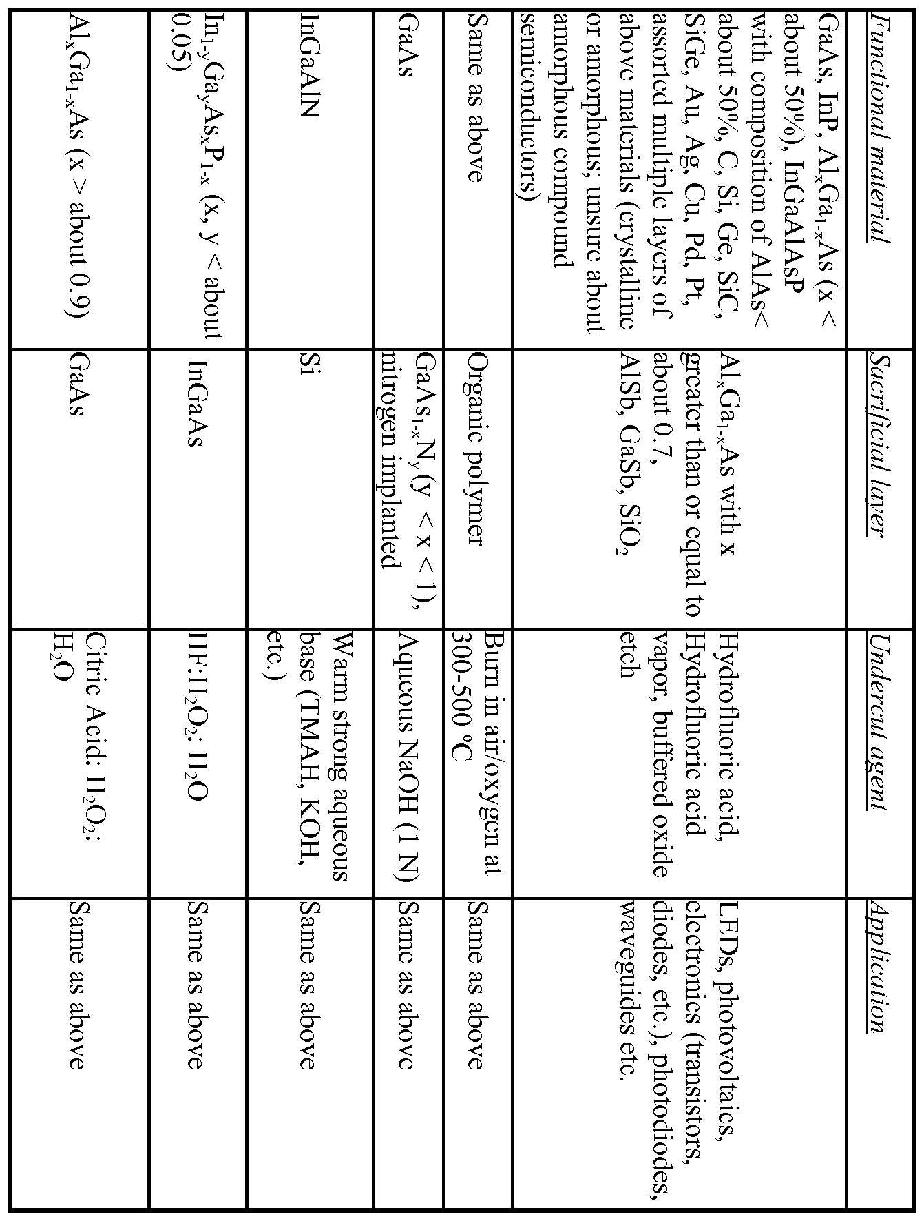
- LED들의 생산에서 유용한 기능 레이어 구성(도 3e 참조)Functional layer construction useful in the production of LEDs (see FIG. 3E).
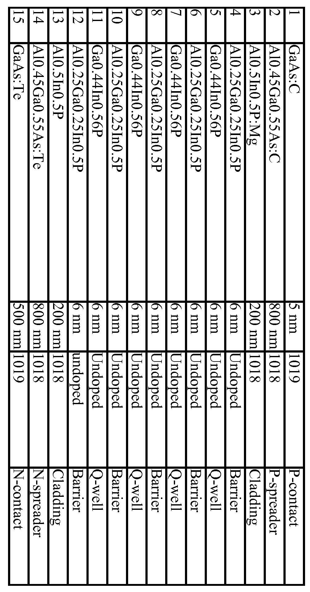
Claims (97)
Applications Claiming Priority (5)
| Application Number | Priority Date | Filing Date | Title |
|---|---|---|---|
| US82635406P | 2006-09-20 | 2006-09-20 | |
| US60/826,354 | 2006-09-20 | ||
| US94465307P | 2007-06-18 | 2007-06-18 | |
| US60/944,653 | 2007-06-18 | ||
| PCT/US2007/079070 WO2008036837A2 (en) | 2006-09-20 | 2007-09-20 | Release strategies for making transferable semiconductor structures, devices and device components |
Related Child Applications (1)
| Application Number | Title | Priority Date | Filing Date |
|---|---|---|---|
| KR1020147001286A Division KR101615255B1 (en) | 2006-09-20 | 2007-09-20 | Release strategies for making transferable semiconductor structures, devices and device components |
Publications (2)
| Publication Number | Publication Date |
|---|---|
| KR20090078803A true KR20090078803A (en) | 2009-07-20 |
| KR101430587B1 KR101430587B1 (en) | 2014-08-14 |
Family
ID=39201282
Family Applications (3)
| Application Number | Title | Priority Date | Filing Date |
|---|---|---|---|
| KR1020147029075A Active KR101588019B1 (en) | 2006-09-20 | 2007-09-20 | Release strategies for making transferable semiconductor structures, devices and device components |
| KR1020097007923A Active KR101430587B1 (en) | 2006-09-20 | 2007-09-20 | Release plans for making transducerable semiconductor structures, devices and device components |
| KR1020147001286A Active KR101615255B1 (en) | 2006-09-20 | 2007-09-20 | Release strategies for making transferable semiconductor structures, devices and device components |
Family Applications Before (1)
| Application Number | Title | Priority Date | Filing Date |
|---|---|---|---|
| KR1020147029075A Active KR101588019B1 (en) | 2006-09-20 | 2007-09-20 | Release strategies for making transferable semiconductor structures, devices and device components |
Family Applications After (1)
| Application Number | Title | Priority Date | Filing Date |
|---|---|---|---|
| KR1020147001286A Active KR101615255B1 (en) | 2006-09-20 | 2007-09-20 | Release strategies for making transferable semiconductor structures, devices and device components |
Country Status (8)
| Country | Link |
|---|---|
| US (4) | US7932123B2 (en) |
| EP (1) | EP2064734B1 (en) |
| JP (3) | JP5319533B2 (en) |
| KR (3) | KR101588019B1 (en) |
| CN (2) | CN103956336B (en) |
| MY (1) | MY149190A (en) |
| TW (1) | TWI438827B (en) |
| WO (1) | WO2008036837A2 (en) |
Cited By (2)
| Publication number | Priority date | Publication date | Assignee | Title |
|---|---|---|---|---|
| KR20140057249A (en) * | 2011-06-28 | 2014-05-12 | 쌩-고벵 크리스톡스 에 드테끄퇴르 | Semiconductor substrate and method of forming |
| KR20180128136A (en) * | 2017-05-23 | 2018-12-03 | 한국기계연구원 | Method for forming a metal pattern using a sacrifice layer |
Families Citing this family (499)
| Publication number | Priority date | Publication date | Assignee | Title |
|---|---|---|---|---|
| US20080055581A1 (en) * | 2004-04-27 | 2008-03-06 | Rogers John A | Devices and methods for pattern generation by ink lithography |
| US7521292B2 (en) | 2004-06-04 | 2009-04-21 | The Board Of Trustees Of The University Of Illinois | Stretchable form of single crystal silicon for high performance electronics on rubber substrates |
| US8217381B2 (en) | 2004-06-04 | 2012-07-10 | The Board Of Trustees Of The University Of Illinois | Controlled buckling structures in semiconductor interconnects and nanomembranes for stretchable electronics |
| KR101307481B1 (en) | 2004-06-04 | 2013-09-26 | 더 보오드 오브 트러스티스 오브 더 유니버시티 오브 일리노이즈 | Methods and devices for fabricating and assembling printable semiconductor elements |
| US7799699B2 (en) | 2004-06-04 | 2010-09-21 | The Board Of Trustees Of The University Of Illinois | Printable semiconductor structures and related methods of making and assembling |
| JP5271541B2 (en) * | 2006-01-16 | 2013-08-21 | パナソニック株式会社 | Semiconductor chip manufacturing method, field effect transistor and manufacturing method thereof |
| US20100047959A1 (en) * | 2006-08-07 | 2010-02-25 | Emcore Solar Power, Inc. | Epitaxial Lift Off on Film Mounted Inverted Metamorphic Multijunction Solar Cells |
| JP5319533B2 (en) | 2006-09-20 | 2013-10-16 | ザ ボード オブ トラスティーズ オブ ザ ユニヴァーシティー オブ イリノイ | Transferable semiconductor structures, devices, and stripping methods for making device components |
| US8005402B2 (en) * | 2007-01-10 | 2011-08-23 | Kabushiki Kaisha Toshiba | Charging device, image forming apparatus and charging method |
| KR101636750B1 (en) | 2007-01-17 | 2016-07-06 | 더 보오드 오브 트러스티스 오브 더 유니버시티 오브 일리노이즈 | Optical systems fabricated by printing-based assembly |
| US8097922B1 (en) * | 2007-05-29 | 2012-01-17 | The Regents Of The University Of California | Nanometer-scale transistor architecture providing enhanced carrier mobility |
| WO2009067347A1 (en) * | 2007-11-20 | 2009-05-28 | Arizona Board Of Regents, Acting For And On Behalf Of Arizona State University | Lattice matched multi- junction photovoltaic and optoelectronic devices |
| TWI723953B (en) | 2008-03-05 | 2021-04-11 | 美國伊利諾大學理事會 | Stretchable and foldable electronic devices |
| US8470701B2 (en) * | 2008-04-03 | 2013-06-25 | Advanced Diamond Technologies, Inc. | Printable, flexible and stretchable diamond for thermal management |
| ES2530458T3 (en) * | 2008-05-12 | 2015-03-03 | Univ Villanova | Solar cells and solar cell manufacturing method |
| KR101405023B1 (en) | 2008-07-04 | 2014-06-10 | 주성엔지니어링(주) | Thin film solar cell and its manufacturing method |
| US7927976B2 (en) | 2008-07-23 | 2011-04-19 | Semprius, Inc. | Reinforced composite stamp for dry transfer printing of semiconductor elements |
| US7999454B2 (en) * | 2008-08-14 | 2011-08-16 | Global Oled Technology Llc | OLED device with embedded chip driving |
| KR20100027526A (en) * | 2008-09-02 | 2010-03-11 | 삼성전기주식회사 | Fabrication method of thin film device |
| US8679888B2 (en) | 2008-09-24 | 2014-03-25 | The Board Of Trustees Of The University Of Illinois | Arrays of ultrathin silicon solar microcells |
| US8389862B2 (en) | 2008-10-07 | 2013-03-05 | Mc10, Inc. | Extremely stretchable electronics |
| US8372726B2 (en) | 2008-10-07 | 2013-02-12 | Mc10, Inc. | Methods and applications of non-planar imaging arrays |
| US8886334B2 (en) | 2008-10-07 | 2014-11-11 | Mc10, Inc. | Systems, methods, and devices using stretchable or flexible electronics for medical applications |
| WO2010042653A1 (en) | 2008-10-07 | 2010-04-15 | Mc10, Inc. | Catheter balloon having stretchable integrated circuitry and sensor array |
| US8097926B2 (en) | 2008-10-07 | 2012-01-17 | Mc10, Inc. | Systems, methods, and devices having stretchable integrated circuitry for sensing and delivering therapy |
| WO2010059781A1 (en) * | 2008-11-19 | 2010-05-27 | Semprius, Inc. | Printing semiconductor elements by shear-assisted elastomeric stamp transfer |
| JP2010135538A (en) * | 2008-12-04 | 2010-06-17 | Sumco Corp | Method of manufacturing bonded wafer |
| US8778199B2 (en) | 2009-02-09 | 2014-07-15 | Emoore Solar Power, Inc. | Epitaxial lift off in inverted metamorphic multijunction solar cells |
| CN102388464B (en) | 2009-02-09 | 2016-09-07 | 森普留斯公司 | Concentrator photovoltaic (CPV) modules, receivers and sub-receivers and methods of forming same |
| US8409911B2 (en) * | 2009-02-24 | 2013-04-02 | Sunpower Corporation | Methods for metallization of solar cells |
| US8877648B2 (en) * | 2009-03-26 | 2014-11-04 | Semprius, Inc. | Methods of forming printable integrated circuit devices by selective etching to suspend the devices from a handling substrate and devices formed thereby |
| US8395191B2 (en) | 2009-10-12 | 2013-03-12 | Monolithic 3D Inc. | Semiconductor device and structure |
| US8362482B2 (en) | 2009-04-14 | 2013-01-29 | Monolithic 3D Inc. | Semiconductor device and structure |
| US8058137B1 (en) | 2009-04-14 | 2011-11-15 | Monolithic 3D Inc. | Method for fabrication of a semiconductor device and structure |
| US9577642B2 (en) | 2009-04-14 | 2017-02-21 | Monolithic 3D Inc. | Method to form a 3D semiconductor device |
| US9509313B2 (en) | 2009-04-14 | 2016-11-29 | Monolithic 3D Inc. | 3D semiconductor device |
| US8754533B2 (en) | 2009-04-14 | 2014-06-17 | Monolithic 3D Inc. | Monolithic three-dimensional semiconductor device and structure |
| US8669778B1 (en) | 2009-04-14 | 2014-03-11 | Monolithic 3D Inc. | Method for design and manufacturing of a 3D semiconductor device |
| US20110199116A1 (en) * | 2010-02-16 | 2011-08-18 | NuPGA Corporation | Method for fabrication of a semiconductor device and structure |
| WO2010129566A1 (en) * | 2009-05-04 | 2010-11-11 | Microlink Devices, Inc. | Assembly techniques for solar cell arrays and solar cells formed therefrom |
| WO2010132552A1 (en) | 2009-05-12 | 2010-11-18 | The Board Of Trustees Of The University Of Illinois | Printed assemblies of ultrathin, microscale inorganic light emitting diodes for deformable and semitransparent displays |
| US8261660B2 (en) | 2009-07-22 | 2012-09-11 | Semprius, Inc. | Vacuum coupled tool apparatus for dry transfer printing semiconductor elements |
| US9165989B2 (en) | 2009-09-16 | 2015-10-20 | Semprius, Inc. | High-yield fabrication of large-format substrates with distributed, independent control elements |
| US9723122B2 (en) | 2009-10-01 | 2017-08-01 | Mc10, Inc. | Protective cases with integrated electronics |
| US10043781B2 (en) | 2009-10-12 | 2018-08-07 | Monolithic 3D Inc. | 3D semiconductor device and structure |
| US10366970B2 (en) | 2009-10-12 | 2019-07-30 | Monolithic 3D Inc. | 3D semiconductor device and structure |
| US10354995B2 (en) | 2009-10-12 | 2019-07-16 | Monolithic 3D Inc. | Semiconductor memory device and structure |
| US9099424B1 (en) | 2012-08-10 | 2015-08-04 | Monolithic 3D Inc. | Semiconductor system, device and structure with heat removal |
| US10157909B2 (en) | 2009-10-12 | 2018-12-18 | Monolithic 3D Inc. | 3D semiconductor device and structure |
| US12027518B1 (en) | 2009-10-12 | 2024-07-02 | Monolithic 3D Inc. | 3D semiconductor devices and structures with metal layers |
| US11374118B2 (en) | 2009-10-12 | 2022-06-28 | Monolithic 3D Inc. | Method to form a 3D integrated circuit |
| US8476145B2 (en) | 2010-10-13 | 2013-07-02 | Monolithic 3D Inc. | Method of fabricating a semiconductor device and structure |
| US8742476B1 (en) | 2012-11-27 | 2014-06-03 | Monolithic 3D Inc. | Semiconductor device and structure |
| US8536023B2 (en) * | 2010-11-22 | 2013-09-17 | Monolithic 3D Inc. | Method of manufacturing a semiconductor device and structure |
| US8294159B2 (en) | 2009-10-12 | 2012-10-23 | Monolithic 3D Inc. | Method for fabrication of a semiconductor device and structure |
| US10910364B2 (en) | 2009-10-12 | 2021-02-02 | Monolitaic 3D Inc. | 3D semiconductor device |
| US11984445B2 (en) | 2009-10-12 | 2024-05-14 | Monolithic 3D Inc. | 3D semiconductor devices and structures with metal layers |
| US11018133B2 (en) | 2009-10-12 | 2021-05-25 | Monolithic 3D Inc. | 3D integrated circuit |
| US10388863B2 (en) | 2009-10-12 | 2019-08-20 | Monolithic 3D Inc. | 3D memory device and structure |
| WO2011069242A1 (en) * | 2009-12-09 | 2011-06-16 | Cooledge Lighting Inc. | Semiconductor dice transfer-enabling apparatus and method for manufacturing transfer-enabling apparatus |
| US8666471B2 (en) | 2010-03-17 | 2014-03-04 | The Board Of Trustees Of The University Of Illinois | Implantable biomedical devices on bioresorbable substrates |
| US9936574B2 (en) | 2009-12-16 | 2018-04-03 | The Board Of Trustees Of The University Of Illinois | Waterproof stretchable optoelectronics |
| US10441185B2 (en) | 2009-12-16 | 2019-10-15 | The Board Of Trustees Of The University Of Illinois | Flexible and stretchable electronic systems for epidermal electronics |
| US10918298B2 (en) | 2009-12-16 | 2021-02-16 | The Board Of Trustees Of The University Of Illinois | High-speed, high-resolution electrophysiology in-vivo using conformal electronics |
| US20110151588A1 (en) * | 2009-12-17 | 2011-06-23 | Cooledge Lighting, Inc. | Method and magnetic transfer stamp for transferring semiconductor dice using magnetic transfer printing techniques |
| US8334152B2 (en) | 2009-12-18 | 2012-12-18 | Cooledge Lighting, Inc. | Method of manufacturing transferable elements incorporating radiation enabled lift off for allowing transfer from host substrate |
| US20110151114A1 (en) * | 2009-12-18 | 2011-06-23 | Cooledge Lighting, Inc. | Composite patterning device and method for removing elements from host substrate by establishing conformal contact between device and a contact surface |
| US8759917B2 (en) * | 2010-01-04 | 2014-06-24 | Samsung Electronics Co., Ltd. | Thin-film transistor having etch stop multi-layer and method of manufacturing the same |
| US8461035B1 (en) | 2010-09-30 | 2013-06-11 | Monolithic 3D Inc. | Method for fabrication of a semiconductor device and structure |
| US9099526B2 (en) | 2010-02-16 | 2015-08-04 | Monolithic 3D Inc. | Integrated circuit device and structure |
| US8492886B2 (en) | 2010-02-16 | 2013-07-23 | Monolithic 3D Inc | 3D integrated circuit with logic |
| US8026521B1 (en) | 2010-10-11 | 2011-09-27 | Monolithic 3D Inc. | Semiconductor device and structure |
| US8541819B1 (en) | 2010-12-09 | 2013-09-24 | Monolithic 3D Inc. | Semiconductor device and structure |
| WO2011112931A1 (en) | 2010-03-12 | 2011-09-15 | The Board Of Trustees Of The University Of Illinois | Waterproof stretchable optoelectronics |
| US9161448B2 (en) | 2010-03-29 | 2015-10-13 | Semprius, Inc. | Laser assisted transfer welding process |
| SG185547A1 (en) | 2010-05-18 | 2012-12-28 | Agency Science Tech & Res | Method of forming a light emitting diode structure and a light emitting diode structure |
| US8525228B2 (en) * | 2010-07-02 | 2013-09-03 | The Regents Of The University Of California | Semiconductor on insulator (XOI) for high performance field effect transistors |
| US8642416B2 (en) | 2010-07-30 | 2014-02-04 | Monolithic 3D Inc. | Method of forming three dimensional integrated circuit devices using layer transfer technique |
| US10217667B2 (en) | 2011-06-28 | 2019-02-26 | Monolithic 3D Inc. | 3D semiconductor device, fabrication method and system |
| US8901613B2 (en) | 2011-03-06 | 2014-12-02 | Monolithic 3D Inc. | Semiconductor device and structure for heat removal |
| US9219005B2 (en) | 2011-06-28 | 2015-12-22 | Monolithic 3D Inc. | Semiconductor system and device |
| US9953925B2 (en) | 2011-06-28 | 2018-04-24 | Monolithic 3D Inc. | Semiconductor system and device |
| WO2012018997A2 (en) | 2010-08-06 | 2012-02-09 | Semprius, Inc. | Materials and processes for releasing printable compound semiconductor devices |
| CN104091862B (en) * | 2010-08-06 | 2017-06-23 | 晶元光电股份有限公司 | Semiconductor optoelectronic element and manufacturing method thereof |
| WO2012027458A1 (en) * | 2010-08-26 | 2012-03-01 | Semprius, Inc. | Structures and methods for testing printable integrated circuits |
| US10497713B2 (en) | 2010-11-18 | 2019-12-03 | Monolithic 3D Inc. | 3D semiconductor memory device and structure |
| US8163581B1 (en) | 2010-10-13 | 2012-04-24 | Monolith IC 3D | Semiconductor and optoelectronic devices |
| US8273610B2 (en) | 2010-11-18 | 2012-09-25 | Monolithic 3D Inc. | Method of constructing a semiconductor device and structure |
| US12362219B2 (en) | 2010-11-18 | 2025-07-15 | Monolithic 3D Inc. | 3D semiconductor memory device and structure |
| US11482440B2 (en) | 2010-12-16 | 2022-10-25 | Monolithic 3D Inc. | 3D semiconductor device and structure with a built-in test circuit for repairing faulty circuits |
| US11158674B2 (en) | 2010-10-11 | 2021-10-26 | Monolithic 3D Inc. | Method to produce a 3D semiconductor device and structure |
| US11257867B1 (en) | 2010-10-11 | 2022-02-22 | Monolithic 3D Inc. | 3D semiconductor device and structure with oxide bonds |
| US11600667B1 (en) | 2010-10-11 | 2023-03-07 | Monolithic 3D Inc. | Method to produce 3D semiconductor devices and structures with memory |
| US11315980B1 (en) | 2010-10-11 | 2022-04-26 | Monolithic 3D Inc. | 3D semiconductor device and structure with transistors |
| US11024673B1 (en) | 2010-10-11 | 2021-06-01 | Monolithic 3D Inc. | 3D semiconductor device and structure |
| US11469271B2 (en) | 2010-10-11 | 2022-10-11 | Monolithic 3D Inc. | Method to produce 3D semiconductor devices and structures with memory |
| US11018191B1 (en) | 2010-10-11 | 2021-05-25 | Monolithic 3D Inc. | 3D semiconductor device and structure |
| US10896931B1 (en) | 2010-10-11 | 2021-01-19 | Monolithic 3D Inc. | 3D semiconductor device and structure |
| US10290682B2 (en) | 2010-10-11 | 2019-05-14 | Monolithic 3D Inc. | 3D IC semiconductor device and structure with stacked memory |
| US11227897B2 (en) | 2010-10-11 | 2022-01-18 | Monolithic 3D Inc. | Method for producing a 3D semiconductor memory device and structure |
| US12360310B2 (en) | 2010-10-13 | 2025-07-15 | Monolithic 3D Inc. | Multilevel semiconductor device and structure with oxide bonding |
| US11133344B2 (en) | 2010-10-13 | 2021-09-28 | Monolithic 3D Inc. | Multilevel semiconductor device and structure with image sensors |
| US11694922B2 (en) | 2010-10-13 | 2023-07-04 | Monolithic 3D Inc. | Multilevel semiconductor device and structure with oxide bonding |
| US12080743B2 (en) | 2010-10-13 | 2024-09-03 | Monolithic 3D Inc. | Multilevel semiconductor device and structure with image sensors and wafer bonding |
| US11929372B2 (en) | 2010-10-13 | 2024-03-12 | Monolithic 3D Inc. | Multilevel semiconductor device and structure with image sensors and wafer bonding |
| US9197804B1 (en) | 2011-10-14 | 2015-11-24 | Monolithic 3D Inc. | Semiconductor and optoelectronic devices |
| US11327227B2 (en) | 2010-10-13 | 2022-05-10 | Monolithic 3D Inc. | Multilevel semiconductor device and structure with electromagnetic modulators |
| US10833108B2 (en) | 2010-10-13 | 2020-11-10 | Monolithic 3D Inc. | 3D microdisplay device and structure |
| US11605663B2 (en) | 2010-10-13 | 2023-03-14 | Monolithic 3D Inc. | Multilevel semiconductor device and structure with image sensors and wafer bonding |
| US11163112B2 (en) | 2010-10-13 | 2021-11-02 | Monolithic 3D Inc. | Multilevel semiconductor device and structure with electromagnetic modulators |
| US10679977B2 (en) | 2010-10-13 | 2020-06-09 | Monolithic 3D Inc. | 3D microdisplay device and structure |
| US11437368B2 (en) | 2010-10-13 | 2022-09-06 | Monolithic 3D Inc. | Multilevel semiconductor device and structure with oxide bonding |
| US11869915B2 (en) | 2010-10-13 | 2024-01-09 | Monolithic 3D Inc. | Multilevel semiconductor device and structure with image sensors and wafer bonding |
| US10998374B1 (en) | 2010-10-13 | 2021-05-04 | Monolithic 3D Inc. | Multilevel semiconductor device and structure |
| US11855100B2 (en) | 2010-10-13 | 2023-12-26 | Monolithic 3D Inc. | Multilevel semiconductor device and structure with oxide bonding |
| US11063071B1 (en) | 2010-10-13 | 2021-07-13 | Monolithic 3D Inc. | Multilevel semiconductor device and structure with waveguides |
| US11043523B1 (en) | 2010-10-13 | 2021-06-22 | Monolithic 3D Inc. | Multilevel semiconductor device and structure with image sensors |
| US20120091474A1 (en) * | 2010-10-13 | 2012-04-19 | NuPGA Corporation | Novel semiconductor and optoelectronic devices |
| US10943934B2 (en) | 2010-10-13 | 2021-03-09 | Monolithic 3D Inc. | Multilevel semiconductor device and structure |
| US10978501B1 (en) | 2010-10-13 | 2021-04-13 | Monolithic 3D Inc. | Multilevel semiconductor device and structure with waveguides |
| US11164898B2 (en) | 2010-10-13 | 2021-11-02 | Monolithic 3D Inc. | Multilevel semiconductor device and structure |
| US11984438B2 (en) | 2010-10-13 | 2024-05-14 | Monolithic 3D Inc. | Multilevel semiconductor device and structure with oxide bonding |
| US11404466B2 (en) | 2010-10-13 | 2022-08-02 | Monolithic 3D Inc. | Multilevel semiconductor device and structure with image sensors |
| US12094892B2 (en) | 2010-10-13 | 2024-09-17 | Monolithic 3D Inc. | 3D micro display device and structure |
| US11855114B2 (en) | 2010-10-13 | 2023-12-26 | Monolithic 3D Inc. | Multilevel semiconductor device and structure with image sensors and wafer bonding |
| US11862503B2 (en) | 2010-11-18 | 2024-01-02 | Monolithic 3D Inc. | Method for producing a 3D semiconductor device and structure with memory cells and multiple metal layers |
| US11482439B2 (en) | 2010-11-18 | 2022-10-25 | Monolithic 3D Inc. | Methods for producing a 3D semiconductor memory device comprising charge trap junction-less transistors |
| US11854857B1 (en) | 2010-11-18 | 2023-12-26 | Monolithic 3D Inc. | Methods for producing a 3D semiconductor device and structure with memory cells and multiple metal layers |
| US12068187B2 (en) | 2010-11-18 | 2024-08-20 | Monolithic 3D Inc. | 3D semiconductor device and structure with bonding and DRAM memory cells |
| US11107721B2 (en) | 2010-11-18 | 2021-08-31 | Monolithic 3D Inc. | 3D semiconductor device and structure with NAND logic |
| US11521888B2 (en) | 2010-11-18 | 2022-12-06 | Monolithic 3D Inc. | 3D semiconductor device and structure with high-k metal gate transistors |
| US11018042B1 (en) | 2010-11-18 | 2021-05-25 | Monolithic 3D Inc. | 3D semiconductor memory device and structure |
| US11495484B2 (en) | 2010-11-18 | 2022-11-08 | Monolithic 3D Inc. | 3D semiconductor devices and structures with at least two single-crystal layers |
| US12100611B2 (en) | 2010-11-18 | 2024-09-24 | Monolithic 3D Inc. | Methods for producing a 3D semiconductor device and structure with memory cells and multiple metal layers |
| US11508605B2 (en) | 2010-11-18 | 2022-11-22 | Monolithic 3D Inc. | 3D semiconductor memory device and structure |
| US12033884B2 (en) | 2010-11-18 | 2024-07-09 | Monolithic 3D Inc. | Methods for producing a 3D semiconductor device and structure with memory cells and multiple metal layers |
| US11443971B2 (en) | 2010-11-18 | 2022-09-13 | Monolithic 3D Inc. | 3D semiconductor device and structure with memory |
| US11004719B1 (en) | 2010-11-18 | 2021-05-11 | Monolithic 3D Inc. | Methods for producing a 3D semiconductor memory device and structure |
| US11735462B2 (en) | 2010-11-18 | 2023-08-22 | Monolithic 3D Inc. | 3D semiconductor device and structure with single-crystal layers |
| US11615977B2 (en) | 2010-11-18 | 2023-03-28 | Monolithic 3D Inc. | 3D semiconductor memory device and structure |
| US12243765B2 (en) | 2010-11-18 | 2025-03-04 | Monolithic 3D Inc. | 3D semiconductor device and structure with metal layers and memory cells |
| US11610802B2 (en) | 2010-11-18 | 2023-03-21 | Monolithic 3D Inc. | Method for producing a 3D semiconductor device and structure with single crystal transistors and metal gate electrodes |
| US11355381B2 (en) | 2010-11-18 | 2022-06-07 | Monolithic 3D Inc. | 3D semiconductor memory device and structure |
| US11482438B2 (en) | 2010-11-18 | 2022-10-25 | Monolithic 3D Inc. | Methods for producing a 3D semiconductor memory device and structure |
| US11164770B1 (en) | 2010-11-18 | 2021-11-02 | Monolithic 3D Inc. | Method for producing a 3D semiconductor memory device and structure |
| US11784082B2 (en) | 2010-11-18 | 2023-10-10 | Monolithic 3D Inc. | 3D semiconductor device and structure with bonding |
| US11094576B1 (en) | 2010-11-18 | 2021-08-17 | Monolithic 3D Inc. | Methods for producing a 3D semiconductor memory device and structure |
| US11355380B2 (en) | 2010-11-18 | 2022-06-07 | Monolithic 3D Inc. | Methods for producing 3D semiconductor memory device and structure utilizing alignment marks |
| US12125737B1 (en) | 2010-11-18 | 2024-10-22 | Monolithic 3D Inc. | 3D semiconductor device and structure with metal layers and memory cells |
| US11121021B2 (en) | 2010-11-18 | 2021-09-14 | Monolithic 3D Inc. | 3D semiconductor device and structure |
| US11031275B2 (en) | 2010-11-18 | 2021-06-08 | Monolithic 3D Inc. | 3D semiconductor device and structure with memory |
| US11923230B1 (en) | 2010-11-18 | 2024-03-05 | Monolithic 3D Inc. | 3D semiconductor device and structure with bonding |
| US11901210B2 (en) | 2010-11-18 | 2024-02-13 | Monolithic 3D Inc. | 3D semiconductor device and structure with memory |
| US12154817B1 (en) | 2010-11-18 | 2024-11-26 | Monolithic 3D Inc. | Methods for producing a 3D semiconductor memory device and structure |
| US11211279B2 (en) | 2010-11-18 | 2021-12-28 | Monolithic 3D Inc. | Method for processing a 3D integrated circuit and structure |
| US12272586B2 (en) | 2010-11-18 | 2025-04-08 | Monolithic 3D Inc. | 3D semiconductor memory device and structure with memory and metal layers |
| US11569117B2 (en) | 2010-11-18 | 2023-01-31 | Monolithic 3D Inc. | 3D semiconductor device and structure with single-crystal layers |
| US12144190B2 (en) | 2010-11-18 | 2024-11-12 | Monolithic 3D Inc. | 3D semiconductor device and structure with bonding and memory cells preliminary class |
| US12136562B2 (en) | 2010-11-18 | 2024-11-05 | Monolithic 3D Inc. | 3D semiconductor device and structure with single-crystal layers |
| US11804396B2 (en) | 2010-11-18 | 2023-10-31 | Monolithic 3D Inc. | Methods for producing a 3D semiconductor device and structure with memory cells and multiple metal layers |
| US9899329B2 (en) | 2010-11-23 | 2018-02-20 | X-Celeprint Limited | Interconnection structures and methods for transfer-printed integrated circuit elements with improved interconnection alignment tolerance |
| US12463076B2 (en) | 2010-12-16 | 2025-11-04 | Monolithic 3D Inc. | 3D semiconductor device and structure |
| US9024310B2 (en) | 2011-01-12 | 2015-05-05 | Tsinghua University | Epitaxial structure |
| US9184319B2 (en) | 2011-01-14 | 2015-11-10 | The Board Of Trustees Of The Leland Stanford Junior University | Multi-terminal multi-junction photovoltaic cells |
| US8932898B2 (en) | 2011-01-14 | 2015-01-13 | The Board Of Trustees Of The Leland Stanford Junior Univerity | Deposition and post-processing techniques for transparent conductive films |
| WO2012097163A1 (en) | 2011-01-14 | 2012-07-19 | The Board Of Trustees Of The University Of Illinois | Optical component array having adjustable curvature |
| US8975670B2 (en) | 2011-03-06 | 2015-03-10 | Monolithic 3D Inc. | Semiconductor device and structure for heat removal |
| US9765934B2 (en) | 2011-05-16 | 2017-09-19 | The Board Of Trustees Of The University Of Illinois | Thermally managed LED arrays assembled by printing |
| EP2712491B1 (en) | 2011-05-27 | 2019-12-04 | Mc10, Inc. | Flexible electronic structure |
| EP2713863B1 (en) | 2011-06-03 | 2020-01-15 | The Board of Trustees of the University of Illionis | Conformable actively multiplexed high-density surface electrode array for brain interfacing |
| US8889485B2 (en) | 2011-06-08 | 2014-11-18 | Semprius, Inc. | Methods for surface attachment of flipped active componenets |
| US10388568B2 (en) | 2011-06-28 | 2019-08-20 | Monolithic 3D Inc. | 3D semiconductor device and system |
| WO2013010113A1 (en) | 2011-07-14 | 2013-01-17 | The Board Of Trustees Of The University Of Illinois | Non-contact transfer printing |
| US9064808B2 (en) * | 2011-07-25 | 2015-06-23 | Synopsys, Inc. | Integrated circuit devices having features with reduced edge curvature and methods for manufacturing the same |
| WO2013020111A1 (en) * | 2011-08-03 | 2013-02-07 | Crystal Solar, Inc. | Photovoltaic module fabrication with thin single crystal epitaxial silicon devices |
| US9793144B2 (en) * | 2011-08-30 | 2017-10-17 | Evatec Ag | Wafer holder and temperature conditioning arrangement and method of manufacturing a wafer |
| US8609550B2 (en) | 2011-09-08 | 2013-12-17 | Synopsys, Inc. | Methods for manufacturing integrated circuit devices having features with reduced edge curvature |
| US9412727B2 (en) | 2011-09-20 | 2016-08-09 | Semprius, Inc. | Printing transferable components using microstructured elastomeric surfaces with pressure modulated reversible adhesion |
| US8492187B2 (en) * | 2011-09-29 | 2013-07-23 | International Business Machines Corporation | High throughput epitaxial liftoff for releasing multiple semiconductor device layers from a single base substrate |
| JP2014532307A (en) * | 2011-09-30 | 2014-12-04 | マイクロリンク デバイシズ,インコーポレーテッド | Light emitting diodes manufactured by epitaxial lift-off |
| US8687399B2 (en) | 2011-10-02 | 2014-04-01 | Monolithic 3D Inc. | Semiconductor device and structure |
| US9029173B2 (en) | 2011-10-18 | 2015-05-12 | Monolithic 3D Inc. | Method for fabrication of a semiconductor device and structure |
| JP5854794B2 (en) * | 2011-11-25 | 2016-02-09 | キヤノン株式会社 | Manufacturing method of organic EL device |
| KR101979354B1 (en) | 2011-12-01 | 2019-08-29 | 더 보오드 오브 트러스티스 오브 더 유니버시티 오브 일리노이즈 | Transient devices designed to undergo programmable transformations |
| JP5680229B2 (en) * | 2012-02-07 | 2015-03-04 | 東京応化工業株式会社 | Processing method and processing apparatus |
| US9000557B2 (en) | 2012-03-17 | 2015-04-07 | Zvi Or-Bach | Semiconductor device and structure |
| WO2013149181A1 (en) | 2012-03-30 | 2013-10-03 | The Board Of Trustees Of The University Of Illinois | Appendage mountable electronic devices conformable to surfaces |
| US11164811B2 (en) | 2012-04-09 | 2021-11-02 | Monolithic 3D Inc. | 3D semiconductor device with isolation layers and oxide-to-oxide bonding |
| US8557632B1 (en) | 2012-04-09 | 2013-10-15 | Monolithic 3D Inc. | Method for fabrication of a semiconductor device and structure |
| US11476181B1 (en) | 2012-04-09 | 2022-10-18 | Monolithic 3D Inc. | 3D semiconductor device and structure with metal layers |
| US11881443B2 (en) | 2012-04-09 | 2024-01-23 | Monolithic 3D Inc. | 3D semiconductor device and structure with metal layers and a connective path |
| US11616004B1 (en) | 2012-04-09 | 2023-03-28 | Monolithic 3D Inc. | 3D semiconductor device and structure with metal layers and a connective path |
| US10600888B2 (en) | 2012-04-09 | 2020-03-24 | Monolithic 3D Inc. | 3D semiconductor device |
| US11694944B1 (en) | 2012-04-09 | 2023-07-04 | Monolithic 3D Inc. | 3D semiconductor device and structure with metal layers and a connective path |
| US11735501B1 (en) | 2012-04-09 | 2023-08-22 | Monolithic 3D Inc. | 3D semiconductor device and structure with metal layers and a connective path |
| US11410912B2 (en) | 2012-04-09 | 2022-08-09 | Monolithic 3D Inc. | 3D semiconductor device with vias and isolation layers |
| US11088050B2 (en) | 2012-04-09 | 2021-08-10 | Monolithic 3D Inc. | 3D semiconductor device with isolation layers |
| US11594473B2 (en) | 2012-04-09 | 2023-02-28 | Monolithic 3D Inc. | 3D semiconductor device and structure with metal layers and a connective path |
| KR20130122089A (en) * | 2012-04-30 | 2013-11-07 | (주)버티클 | Methods of manufacturing semiconductor devices |
| JPWO2014017063A1 (en) * | 2012-07-24 | 2016-07-07 | 住友化学株式会社 | Semiconductor substrate, semiconductor substrate manufacturing method, and composite substrate manufacturing method |
| KR101878754B1 (en) | 2012-09-13 | 2018-07-17 | 삼성전자주식회사 | Method of manufacturing large area gallium nitride substrate |
| US8946052B2 (en) * | 2012-09-26 | 2015-02-03 | Sandia Corporation | Processes for multi-layer devices utilizing layer transfer |
| US9171794B2 (en) | 2012-10-09 | 2015-10-27 | Mc10, Inc. | Embedding thin chips in polymer |
| EP2731126A1 (en) | 2012-11-09 | 2014-05-14 | Nederlandse Organisatie voor toegepast -natuurwetenschappelijk onderzoek TNO | Method for bonding bare chip dies |
| US8574929B1 (en) | 2012-11-16 | 2013-11-05 | Monolithic 3D Inc. | Method to form a 3D semiconductor device and structure |
| US8686428B1 (en) | 2012-11-16 | 2014-04-01 | Monolithic 3D Inc. | Semiconductor device and structure |
| US11916045B2 (en) | 2012-12-22 | 2024-02-27 | Monolithic 3D Inc. | 3D semiconductor device and structure with metal layers |
| US11967583B2 (en) | 2012-12-22 | 2024-04-23 | Monolithic 3D Inc. | 3D semiconductor device and structure with metal layers |
| US8674470B1 (en) | 2012-12-22 | 2014-03-18 | Monolithic 3D Inc. | Semiconductor device and structure |
| US12051674B2 (en) | 2012-12-22 | 2024-07-30 | Monolithic 3D Inc. | 3D semiconductor device and structure with metal layers |
| US11063024B1 (en) | 2012-12-22 | 2021-07-13 | Monlithic 3D Inc. | Method to form a 3D semiconductor device and structure |
| US11961827B1 (en) | 2012-12-22 | 2024-04-16 | Monolithic 3D Inc. | 3D semiconductor device and structure with metal layers |
| US11309292B2 (en) | 2012-12-22 | 2022-04-19 | Monolithic 3D Inc. | 3D semiconductor device and structure with metal layers |
| US11217565B2 (en) | 2012-12-22 | 2022-01-04 | Monolithic 3D Inc. | Method to form a 3D semiconductor device and structure |
| US11018116B2 (en) | 2012-12-22 | 2021-05-25 | Monolithic 3D Inc. | Method to form a 3D semiconductor device and structure |
| US11784169B2 (en) | 2012-12-22 | 2023-10-10 | Monolithic 3D Inc. | 3D semiconductor device and structure with metal layers |
| KR20140085198A (en) * | 2012-12-27 | 2014-07-07 | 서울바이오시스 주식회사 | Method for separating substrate and method for fabricating semiconductor device using mask pattern |
| US12249538B2 (en) | 2012-12-29 | 2025-03-11 | Monolithic 3D Inc. | 3D semiconductor device and structure including power distribution grids |
| US9385058B1 (en) | 2012-12-29 | 2016-07-05 | Monolithic 3D Inc. | Semiconductor device and structure |
| US11430668B2 (en) | 2012-12-29 | 2022-08-30 | Monolithic 3D Inc. | 3D semiconductor device and structure with bonding |
| US10892169B2 (en) | 2012-12-29 | 2021-01-12 | Monolithic 3D Inc. | 3D semiconductor device and structure |
| US10115663B2 (en) | 2012-12-29 | 2018-10-30 | Monolithic 3D Inc. | 3D semiconductor device and structure |
| US10600657B2 (en) | 2012-12-29 | 2020-03-24 | Monolithic 3D Inc | 3D semiconductor device and structure |
| US10651054B2 (en) | 2012-12-29 | 2020-05-12 | Monolithic 3D Inc. | 3D semiconductor device and structure |
| US11004694B1 (en) | 2012-12-29 | 2021-05-11 | Monolithic 3D Inc. | 3D semiconductor device and structure |
| US10903089B1 (en) | 2012-12-29 | 2021-01-26 | Monolithic 3D Inc. | 3D semiconductor device and structure |
| US11087995B1 (en) | 2012-12-29 | 2021-08-10 | Monolithic 3D Inc. | 3D semiconductor device and structure |
| US11430667B2 (en) | 2012-12-29 | 2022-08-30 | Monolithic 3D Inc. | 3D semiconductor device and structure with bonding |
| US9871034B1 (en) | 2012-12-29 | 2018-01-16 | Monolithic 3D Inc. | Semiconductor device and structure |
| US11177140B2 (en) | 2012-12-29 | 2021-11-16 | Monolithic 3D Inc. | 3D semiconductor device and structure |
| US9613911B2 (en) | 2013-02-06 | 2017-04-04 | The Board Of Trustees Of The University Of Illinois | Self-similar and fractal design for stretchable electronics |
| US10497633B2 (en) | 2013-02-06 | 2019-12-03 | The Board Of Trustees Of The University Of Illinois | Stretchable electronic systems with fluid containment |
| US10840536B2 (en) | 2013-02-06 | 2020-11-17 | The Board Of Trustees Of The University Of Illinois | Stretchable electronic systems with containment chambers |
| WO2014126927A1 (en) | 2013-02-13 | 2014-08-21 | The Board Of Trustees Of The University Of Illinois | Injectable and implantable cellular-scale electronic devices |
| US9875974B2 (en) | 2013-03-08 | 2018-01-23 | The Board Of Trustees Of The University Of Illinois | Processing techniques for silicon-based transient devices |
| US9875935B2 (en) | 2013-03-08 | 2018-01-23 | Infineon Technologies Austria Ag | Semiconductor device and method for producing the same |
| US12094965B2 (en) | 2013-03-11 | 2024-09-17 | Monolithic 3D Inc. | 3D semiconductor device and structure with metal layers and memory cells |
| US11935949B1 (en) | 2013-03-11 | 2024-03-19 | Monolithic 3D Inc. | 3D semiconductor device and structure with metal layers and memory cells |
| US8902663B1 (en) | 2013-03-11 | 2014-12-02 | Monolithic 3D Inc. | Method of maintaining a memory state |
| US11869965B2 (en) | 2013-03-11 | 2024-01-09 | Monolithic 3D Inc. | 3D semiconductor device and structure with metal layers and memory cells |
| US10325651B2 (en) | 2013-03-11 | 2019-06-18 | Monolithic 3D Inc. | 3D semiconductor device with stacked memory |
| US8994404B1 (en) | 2013-03-12 | 2015-03-31 | Monolithic 3D Inc. | Semiconductor device and structure |
| US11923374B2 (en) | 2013-03-12 | 2024-03-05 | Monolithic 3D Inc. | 3D semiconductor device and structure with metal layers |
| US11088130B2 (en) | 2014-01-28 | 2021-08-10 | Monolithic 3D Inc. | 3D semiconductor device and structure |
| US11398569B2 (en) | 2013-03-12 | 2022-07-26 | Monolithic 3D Inc. | 3D semiconductor device and structure |
| US12100646B2 (en) | 2013-03-12 | 2024-09-24 | Monolithic 3D Inc. | 3D semiconductor device and structure with metal layers |
| US10840239B2 (en) | 2014-08-26 | 2020-11-17 | Monolithic 3D Inc. | 3D semiconductor device and structure |
| US9580302B2 (en) | 2013-03-15 | 2017-02-28 | Versana Micro Inc. | Cell phone having a monolithically integrated multi-sensor device on a semiconductor substrate and method therefor |
| WO2014145930A1 (en) * | 2013-03-15 | 2014-09-18 | Amberwave, Inc. | Solar cell |
| US10224279B2 (en) | 2013-03-15 | 2019-03-05 | Monolithic 3D Inc. | Semiconductor device and structure |
| US9117749B1 (en) | 2013-03-15 | 2015-08-25 | Monolithic 3D Inc. | Semiconductor device and structure |
| WO2014165686A2 (en) | 2013-04-04 | 2014-10-09 | The Board Of Trustees Of The University Of Illinois | Purification of carbon nanotubes via selective heating |
| US10292263B2 (en) | 2013-04-12 | 2019-05-14 | The Board Of Trustees Of The University Of Illinois | Biodegradable materials for multilayer transient printed circuit boards |
| AU2014250839B2 (en) | 2013-04-12 | 2018-05-10 | The Board Of Trustees Of The University Of Illinois | Inorganic and organic transient electronic devices |
| US11720736B2 (en) | 2013-04-15 | 2023-08-08 | Monolithic 3D Inc. | Automation methods for 3D integrated circuits and devices |
| US11030371B2 (en) | 2013-04-15 | 2021-06-08 | Monolithic 3D Inc. | Automation for monolithic 3D devices |
| US11270055B1 (en) | 2013-04-15 | 2022-03-08 | Monolithic 3D Inc. | Automation for monolithic 3D devices |
| US11341309B1 (en) | 2013-04-15 | 2022-05-24 | Monolithic 3D Inc. | Automation for monolithic 3D devices |
| US11574109B1 (en) | 2013-04-15 | 2023-02-07 | Monolithic 3D Inc | Automation methods for 3D integrated circuits and devices |
| US9021414B1 (en) | 2013-04-15 | 2015-04-28 | Monolithic 3D Inc. | Automation for monolithic 3D devices |
| US11487928B2 (en) | 2013-04-15 | 2022-11-01 | Monolithic 3D Inc. | Automation for monolithic 3D devices |
| WO2015006382A1 (en) * | 2013-07-08 | 2015-01-15 | Solexel, Inc. | Thin film solar cell lamination stack for high volume manufacturing |
| KR20160067152A (en) | 2013-10-02 | 2016-06-13 | 더 보드 오브 트러스티즈 오브 더 유니버시티 오브 일리노이 | Organ mounted electronics |
| WO2015084868A1 (en) * | 2013-12-02 | 2015-06-11 | The Regents Of The University Of Michigan | Fabrication of thin-film electronic devices with non-destructive wafer reuse |
| US9058990B1 (en) * | 2013-12-19 | 2015-06-16 | International Business Machines Corporation | Controlled spalling of group III nitrides containing an embedded spall releasing plane |
| JP6570009B2 (en) * | 2014-01-15 | 2019-09-04 | ザ リージェンツ オブ ザ ユニヴァシティ オブ ミシガン | Integration of epitaxial lift-off solar cells with a small parabolic concentrator by printing method |
| US12094829B2 (en) | 2014-01-28 | 2024-09-17 | Monolithic 3D Inc. | 3D semiconductor device and structure |
| US11107808B1 (en) | 2014-01-28 | 2021-08-31 | Monolithic 3D Inc. | 3D semiconductor device and structure |
| US11031394B1 (en) | 2014-01-28 | 2021-06-08 | Monolithic 3D Inc. | 3D semiconductor device and structure |
| US10297586B2 (en) | 2015-03-09 | 2019-05-21 | Monolithic 3D Inc. | Methods for processing a 3D semiconductor device |
| US9129863B2 (en) | 2014-02-11 | 2015-09-08 | International Business Machines Corporation | Method to form dual channel group III-V and Si/Ge FINFET CMOS |
| US9123585B1 (en) | 2014-02-11 | 2015-09-01 | International Business Machines Corporation | Method to form group III-V and Si/Ge FINFET on insulator |
| US9236565B2 (en) * | 2014-04-29 | 2016-01-12 | National University Of Singapore | Method for fabricating a magnetoresistive device |
| US9274277B2 (en) | 2014-05-15 | 2016-03-01 | Globalfoundries Inc. | Waveguide devices with supporting anchors |
| TWI677963B (en) | 2014-06-18 | 2019-11-21 | 愛爾蘭商艾克斯瑟樂普林特有限公司 | Micro assembled high frequency devices and arrays |
| US9865600B2 (en) | 2014-06-18 | 2018-01-09 | X-Celeprint Limited | Printed capacitors |
| CN113035850B (en) | 2014-06-18 | 2022-12-06 | 艾克斯展示公司技术有限公司 | Micro-assembly LED display |
| US9761754B2 (en) | 2014-06-18 | 2017-09-12 | X-Celeprint Limited | Systems and methods for preparing GaN and related materials for micro assembly |
| US9929053B2 (en) | 2014-06-18 | 2018-03-27 | X-Celeprint Limited | Systems and methods for controlling release of transferable semiconductor structures |
| EP3157858B1 (en) * | 2014-06-18 | 2018-12-26 | X-Celeprint Limited | Systems and methods for controlling release of transferable semiconductor structures |
| KR102181010B1 (en) | 2014-07-20 | 2020-11-20 | 엑스-셀레프린트 리미티드 | Apparatus and methods for micro-transfer printing |
| US9111983B1 (en) | 2014-07-31 | 2015-08-18 | Freescale Semiconductor, Inc. | Methods for removing adhesive layers from semiconductor wafers |
| KR20170041291A (en) | 2014-08-11 | 2017-04-14 | 더 보오드 오브 트러스티스 오브 더 유니버시티 오브 일리노이즈 | Devices and related methods for epidermal characterization of biofluids |
| US11160458B2 (en) | 2014-08-11 | 2021-11-02 | The Board Of Trustees Of The University Of Illinois | Epidermal devices for analysis of temperature and thermal transport characteristics |
| WO2016025430A1 (en) | 2014-08-11 | 2016-02-18 | The Board Of Trustees Of The University Of Illinois | Epidermal photonic systems and methods |
| WO2016030422A1 (en) | 2014-08-26 | 2016-03-03 | X-Celeprint Limited | Micro assembled hybrid displays and lighting elements |
| US9991163B2 (en) | 2014-09-25 | 2018-06-05 | X-Celeprint Limited | Small-aperture-ratio display with electrical component |
| US9799261B2 (en) | 2014-09-25 | 2017-10-24 | X-Celeprint Limited | Self-compensating circuit for faulty display pixels |
| US9799719B2 (en) | 2014-09-25 | 2017-10-24 | X-Celeprint Limited | Active-matrix touchscreen |
| US9468050B1 (en) | 2014-09-25 | 2016-10-11 | X-Celeprint Limited | Self-compensating circuit for faulty display pixels |
| US9818725B2 (en) | 2015-06-01 | 2017-11-14 | X-Celeprint Limited | Inorganic-light-emitter display with integrated black matrix |
| US9537069B1 (en) | 2014-09-25 | 2017-01-03 | X-Celeprint Limited | Inorganic light-emitting diode with encapsulating reflector |
| US9922956B2 (en) * | 2014-09-26 | 2018-03-20 | Qualcomm Incorporated | Microelectromechanical system (MEMS) bond release structure and method of wafer transfer for three-dimensional integrated circuit (3D IC) integration |
| US10538028B2 (en) | 2014-11-17 | 2020-01-21 | The Board Of Trustees Of The University Of Illinois | Deterministic assembly of complex, three-dimensional architectures by compressive buckling |
| DE112016000533B4 (en) * | 2015-01-30 | 2024-06-27 | OSRAM Opto Semiconductors Gesellschaft mit beschränkter Haftung | Method for producing a semiconductor device and semiconductor device |
| TW201705515A (en) * | 2015-03-18 | 2017-02-01 | 美國密西根州立大學 | Strain release epitaxial lift-off by pre-patterned convex surface |
| US12477752B2 (en) | 2015-09-21 | 2025-11-18 | Monolithic 3D Inc. | 3D semiconductor memory devices and structures |
| US11011507B1 (en) | 2015-04-19 | 2021-05-18 | Monolithic 3D Inc. | 3D semiconductor device and structure |
| US11937422B2 (en) | 2015-11-07 | 2024-03-19 | Monolithic 3D Inc. | Semiconductor memory device and structure |
| US10825779B2 (en) | 2015-04-19 | 2020-11-03 | Monolithic 3D Inc. | 3D semiconductor device and structure |
| US11056468B1 (en) | 2015-04-19 | 2021-07-06 | Monolithic 3D Inc. | 3D semiconductor device and structure |
| US10515981B2 (en) | 2015-09-21 | 2019-12-24 | Monolithic 3D Inc. | Multilevel semiconductor device and structure with memory |
| US11978731B2 (en) | 2015-09-21 | 2024-05-07 | Monolithic 3D Inc. | Method to produce a multi-level semiconductor memory device and structure |
| US11114427B2 (en) | 2015-11-07 | 2021-09-07 | Monolithic 3D Inc. | 3D semiconductor processor and memory device and structure |
| US10381328B2 (en) | 2015-04-19 | 2019-08-13 | Monolithic 3D Inc. | Semiconductor device and structure |
| US9640715B2 (en) | 2015-05-15 | 2017-05-02 | X-Celeprint Limited | Printable inorganic semiconductor structures |
| MX2017015587A (en) | 2015-06-01 | 2018-08-23 | Univ Illinois | ALTERNATIVE METHOD FOR UV SENSOR. |
| BR112017025609A2 (en) | 2015-06-01 | 2018-08-07 | The Board Of Trustees Of The University Of Illinois | miniaturized wireless electronic systems with near field communication capabilities |
| US9871345B2 (en) | 2015-06-09 | 2018-01-16 | X-Celeprint Limited | Crystalline color-conversion device |
| US10102794B2 (en) | 2015-06-09 | 2018-10-16 | X-Celeprint Limited | Distributed charge-pump power-supply system |
| US11061276B2 (en) | 2015-06-18 | 2021-07-13 | X Display Company Technology Limited | Laser array display |
| US10133426B2 (en) | 2015-06-18 | 2018-11-20 | X-Celeprint Limited | Display with micro-LED front light |
| US9640391B2 (en) * | 2015-06-23 | 2017-05-02 | The Trustees Of The Stevens Institute Of Technology | Direct and pre-patterned synthesis of two-dimensional heterostructures |
| WO2017004576A1 (en) | 2015-07-02 | 2017-01-05 | The Board Of Trustees Of The University Of Illinois | Wireless optofluidic systems for programmable in vivo pharmacology and optogenetics |
| US9704821B2 (en) | 2015-08-11 | 2017-07-11 | X-Celeprint Limited | Stamp with structured posts |
| US10255834B2 (en) | 2015-07-23 | 2019-04-09 | X-Celeprint Limited | Parallel redundant chiplet system for controlling display pixels |
| US10468363B2 (en) | 2015-08-10 | 2019-11-05 | X-Celeprint Limited | Chiplets with connection posts |
| US9640108B2 (en) | 2015-08-25 | 2017-05-02 | X-Celeprint Limited | Bit-plane pulse width modulated digital display system |
| US11956952B2 (en) | 2015-08-23 | 2024-04-09 | Monolithic 3D Inc. | Semiconductor memory device and structure |
| US10380930B2 (en) | 2015-08-24 | 2019-08-13 | X-Celeprint Limited | Heterogeneous light emitter display system |
| US9899556B2 (en) | 2015-09-14 | 2018-02-20 | Wisconsin Alumni Research Foundation | Hybrid tandem solar cells with improved tunnel junction structures |
| US12100658B2 (en) | 2015-09-21 | 2024-09-24 | Monolithic 3D Inc. | Method to produce a 3D multilayer semiconductor device and structure |
| US12250830B2 (en) | 2015-09-21 | 2025-03-11 | Monolithic 3D Inc. | 3D semiconductor memory devices and structures |
| US12178055B2 (en) | 2015-09-21 | 2024-12-24 | Monolithic 3D Inc. | 3D semiconductor memory devices and structures |
| US10230048B2 (en) | 2015-09-29 | 2019-03-12 | X-Celeprint Limited | OLEDs for micro transfer printing |
| US10418501B2 (en) | 2015-10-02 | 2019-09-17 | X-Celeprint Limited | Wafer-integrated, ultra-low profile concentrated photovoltaics (CPV) for space applications |
| US10522225B1 (en) | 2015-10-02 | 2019-12-31 | Monolithic 3D Inc. | Semiconductor device with non-volatile memory |
| TWI716473B (en) * | 2015-10-22 | 2021-01-21 | 愛爾蘭商艾克斯展示公司技術有限公司 | Array of micro devices |
| US10847540B2 (en) | 2015-10-24 | 2020-11-24 | Monolithic 3D Inc. | 3D semiconductor memory device and structure |
| US11114464B2 (en) | 2015-10-24 | 2021-09-07 | Monolithic 3D Inc. | 3D semiconductor device and structure |
| US12120880B1 (en) | 2015-10-24 | 2024-10-15 | Monolithic 3D Inc. | 3D semiconductor device and structure with logic and memory |
| US12035531B2 (en) | 2015-10-24 | 2024-07-09 | Monolithic 3D Inc. | 3D semiconductor device and structure with logic and memory |
| US12219769B2 (en) | 2015-10-24 | 2025-02-04 | Monolithic 3D Inc. | 3D semiconductor device and structure with logic and memory |
| US11991884B1 (en) | 2015-10-24 | 2024-05-21 | Monolithic 3D Inc. | 3D semiconductor device and structure with logic and memory |
| US11296115B1 (en) | 2015-10-24 | 2022-04-05 | Monolithic 3D Inc. | 3D semiconductor device and structure |
| US10418369B2 (en) | 2015-10-24 | 2019-09-17 | Monolithic 3D Inc. | Multi-level semiconductor memory device and structure |
| US12016181B2 (en) | 2015-10-24 | 2024-06-18 | Monolithic 3D Inc. | 3D semiconductor device and structure with logic and memory |
| US10925543B2 (en) | 2015-11-11 | 2021-02-23 | The Board Of Trustees Of The University Of Illinois | Bioresorbable silicon electronics for transient implants |
| US10066819B2 (en) | 2015-12-09 | 2018-09-04 | X-Celeprint Limited | Micro-light-emitting diode backlight system |
| US10091446B2 (en) | 2015-12-23 | 2018-10-02 | X-Celeprint Limited | Active-matrix displays with common pixel control |
| US9930277B2 (en) | 2015-12-23 | 2018-03-27 | X-Celeprint Limited | Serial row-select matrix-addressed system |
| US9786646B2 (en) | 2015-12-23 | 2017-10-10 | X-Celeprint Limited | Matrix addressed device repair |
| US9928771B2 (en) | 2015-12-24 | 2018-03-27 | X-Celeprint Limited | Distributed pulse width modulation control |
| CN105609589B (en) * | 2016-01-29 | 2017-11-03 | 中国科学院半导体研究所 | Suitable for the preparation method of the inorganic semiconductor film functional unit of transfer |
| US11230471B2 (en) | 2016-02-05 | 2022-01-25 | X-Celeprint Limited | Micro-transfer-printed compound sensor device |
| US10200013B2 (en) | 2016-02-18 | 2019-02-05 | X-Celeprint Limited | Micro-transfer-printed acoustic wave filter device |
| US10361677B2 (en) | 2016-02-18 | 2019-07-23 | X-Celeprint Limited | Transverse bulk acoustic wave filter |
| US10109753B2 (en) | 2016-02-19 | 2018-10-23 | X-Celeprint Limited | Compound micro-transfer-printed optical filter device |
| TWI681508B (en) | 2016-02-25 | 2020-01-01 | 愛爾蘭商艾克斯瑟樂普林特有限公司 | Efficiently micro-transfer printing micro-scale devices onto large-format substrates |
| US10193025B2 (en) | 2016-02-29 | 2019-01-29 | X-Celeprint Limited | Inorganic LED pixel structure |
| US10150325B2 (en) | 2016-02-29 | 2018-12-11 | X-Celeprint Limited | Hybrid banknote with electronic indicia |
| US10150326B2 (en) | 2016-02-29 | 2018-12-11 | X-Celeprint Limited | Hybrid document with variable state |
| KR102323389B1 (en) * | 2016-03-02 | 2021-11-05 | 도쿄엘렉트론가부시키가이샤 | Isotropic silicon and silicon-germanium etching with tunable selectivity |
| US10153257B2 (en) | 2016-03-03 | 2018-12-11 | X-Celeprint Limited | Micro-printed display |
| US10153256B2 (en) | 2016-03-03 | 2018-12-11 | X-Celeprint Limited | Micro-transfer printable electronic component |
| US10917953B2 (en) | 2016-03-21 | 2021-02-09 | X Display Company Technology Limited | Electrically parallel fused LEDs |
| US11154201B2 (en) | 2016-04-01 | 2021-10-26 | The Board Of Trustees Of The University Of Illinois | Implantable medical devices for optogenetics |
| US10103069B2 (en) | 2016-04-01 | 2018-10-16 | X-Celeprint Limited | Pressure-activated electrical interconnection by micro-transfer printing |
| US10008483B2 (en) | 2016-04-05 | 2018-06-26 | X-Celeprint Limited | Micro-transfer printed LED and color filter structure |
| US10199546B2 (en) | 2016-04-05 | 2019-02-05 | X-Celeprint Limited | Color-filter device |
| US9997102B2 (en) | 2016-04-19 | 2018-06-12 | X-Celeprint Limited | Wirelessly powered display and system |
| US10198890B2 (en) | 2016-04-19 | 2019-02-05 | X-Celeprint Limited | Hybrid banknote with electronic indicia using near-field-communications |
| US10360846B2 (en) | 2016-05-10 | 2019-07-23 | X-Celeprint Limited | Distributed pulse-width modulation system with multi-bit digital storage and output device |
| US10622700B2 (en) | 2016-05-18 | 2020-04-14 | X-Celeprint Limited | Antenna with micro-transfer-printed circuit element |
| DE102016109459B4 (en) | 2016-05-23 | 2019-06-13 | X-Fab Semiconductor Foundries Ag | Optimized transfer print (transfer printing) between carrier substrates as process, carrier substrate and micro-technical component |
| DE102016109950B3 (en) | 2016-05-30 | 2017-09-28 | X-Fab Semiconductor Foundries Ag | Integrated circuit having a component applied by a transfer pressure and method for producing the integrated circuit |
| US9997501B2 (en) | 2016-06-01 | 2018-06-12 | X-Celeprint Limited | Micro-transfer-printed light-emitting diode device |
| US10453826B2 (en) | 2016-06-03 | 2019-10-22 | X-Celeprint Limited | Voltage-balanced serial iLED pixel and display |
| US11137641B2 (en) | 2016-06-10 | 2021-10-05 | X Display Company Technology Limited | LED structure with polarized light emission |
| US10653342B2 (en) | 2016-06-17 | 2020-05-19 | The Board Of Trustees Of The University Of Illinois | Soft, wearable microfluidic systems capable of capture, storage, and sensing of biofluids |
| US9966301B2 (en) * | 2016-06-27 | 2018-05-08 | New Fab, LLC | Reduced substrate effects in monolithically integrated RF circuits |
| DE102016117030B4 (en) | 2016-07-17 | 2018-07-05 | X-Fab Semiconductor Foundries Ag | Production of Semiconductor Structures on a Carrier Substrate Transferable by Transfer Print. |
| US10475876B2 (en) | 2016-07-26 | 2019-11-12 | X-Celeprint Limited | Devices with a single metal layer |
| US10222698B2 (en) | 2016-07-28 | 2019-03-05 | X-Celeprint Limited | Chiplets with wicking posts |
| US11064609B2 (en) | 2016-08-04 | 2021-07-13 | X Display Company Technology Limited | Printable 3D electronic structure |
| US9722134B1 (en) * | 2016-08-16 | 2017-08-01 | Mikro Mesa Technology Co., Ltd. | Method for transferring semiconductor structure |
| US9997399B2 (en) * | 2016-08-16 | 2018-06-12 | Mikro Mesa Technology Co., Ltd. | Method for transferring semiconductor structure |
| US9980341B2 (en) | 2016-09-22 | 2018-05-22 | X-Celeprint Limited | Multi-LED components |
| US10157880B2 (en) | 2016-10-03 | 2018-12-18 | X-Celeprint Limited | Micro-transfer printing with volatile adhesive layer |
| US11251149B2 (en) | 2016-10-10 | 2022-02-15 | Monolithic 3D Inc. | 3D memory device and structure |
| US11869591B2 (en) | 2016-10-10 | 2024-01-09 | Monolithic 3D Inc. | 3D memory devices and structures with control circuits |
| US12225704B2 (en) | 2016-10-10 | 2025-02-11 | Monolithic 3D Inc. | 3D memory devices and structures with memory arrays and metal layers |
| US11812620B2 (en) | 2016-10-10 | 2023-11-07 | Monolithic 3D Inc. | 3D DRAM memory devices and structures with control circuits |
| US11930648B1 (en) | 2016-10-10 | 2024-03-12 | Monolithic 3D Inc. | 3D memory devices and structures with metal layers |
| US11329059B1 (en) | 2016-10-10 | 2022-05-10 | Monolithic 3D Inc. | 3D memory devices and structures with thinned single crystal substrates |
| US11711928B2 (en) | 2016-10-10 | 2023-07-25 | Monolithic 3D Inc. | 3D memory devices and structures with control circuits |
| US10782002B2 (en) | 2016-10-28 | 2020-09-22 | X Display Company Technology Limited | LED optical components |
| WO2018085371A1 (en) | 2016-11-01 | 2018-05-11 | Massachusetts Institute Of Technology | Lift-off embedded micro and structures |
| US11027462B2 (en) | 2016-11-09 | 2021-06-08 | The Board Of Trustees Of Western Michigan University | Polydimethylsiloxane films and method of manufacture |
| US10347168B2 (en) | 2016-11-10 | 2019-07-09 | X-Celeprint Limited | Spatially dithered high-resolution |
| US10395966B2 (en) | 2016-11-15 | 2019-08-27 | X-Celeprint Limited | Micro-transfer-printable flip-chip structures and methods |
| US10600671B2 (en) | 2016-11-15 | 2020-03-24 | X-Celeprint Limited | Micro-transfer-printable flip-chip structures and methods |
| US10224231B2 (en) | 2016-11-15 | 2019-03-05 | X-Celeprint Limited | Micro-transfer-printable flip-chip structures and methods |
| CN109952189A (en) | 2016-11-17 | 2019-06-28 | 奥博泰克有限公司 | Hybrid more material 3D printings |
| US10297502B2 (en) | 2016-12-19 | 2019-05-21 | X-Celeprint Limited | Isolation structure for micro-transfer-printable devices |
| US10438859B2 (en) | 2016-12-19 | 2019-10-08 | X-Celeprint Limited | Transfer printed device repair |
| KR101925565B1 (en) * | 2016-12-30 | 2018-12-06 | (재)한국나노기술원 | ELO method using crack pattern |
| US10832609B2 (en) * | 2017-01-10 | 2020-11-10 | X Display Company Technology Limited | Digital-drive pulse-width-modulated output system |
| US10332868B2 (en) | 2017-01-26 | 2019-06-25 | X-Celeprint Limited | Stacked pixel structures |
| US10468391B2 (en) | 2017-02-08 | 2019-11-05 | X-Celeprint Limited | Inorganic light-emitting-diode displays with multi-ILED pixels |
| TWI675402B (en) * | 2017-02-17 | 2019-10-21 | 美商美國亞德諾半導體公司 | Transfer printing method and parallel transfer printing method |
| US10249739B2 (en) | 2017-03-01 | 2019-04-02 | International Business Machines Corporation | Nanosheet MOSFET with partial release and source/drain epitaxy |
| US10396137B2 (en) | 2017-03-10 | 2019-08-27 | X-Celeprint Limited | Testing transfer-print micro-devices on wafer |
| KR101898858B1 (en) * | 2017-03-13 | 2018-10-29 | 주식회사 페타룩스 | Solar cell |
| US11024608B2 (en) | 2017-03-28 | 2021-06-01 | X Display Company Technology Limited | Structures and methods for electrical connection of micro-devices and substrates |
| DE102017108136B4 (en) | 2017-04-13 | 2019-03-14 | X-Fab Semiconductor Foundries Ag | Geometrically shaped components in a transfer printing arrangement and associated methods |
| US10468397B2 (en) | 2017-05-05 | 2019-11-05 | X-Celeprint Limited | Matrix addressed tiles and arrays |
| US10777700B2 (en) * | 2017-06-02 | 2020-09-15 | Wisconsin Alumni Research Foundation | Optoelectronic devices based on thin single-crystalline semiconductor films and non-epitaxial optical cavities |
| CN107188115B (en) * | 2017-06-06 | 2020-05-01 | 北京航空航天大学 | Preparation method of metal/polymer composite three-dimensional micro-nano structure |
| US10176991B1 (en) | 2017-07-06 | 2019-01-08 | Wisconsin Alumni Research Foundation | High-quality, single-crystalline silicon-germanium films |
| US10804880B2 (en) | 2018-12-03 | 2020-10-13 | X-Celeprint Limited | Device structures with acoustic wave transducers and connection posts |
| US10943946B2 (en) | 2017-07-21 | 2021-03-09 | X Display Company Technology Limited | iLED displays with substrate holes |
| US10832935B2 (en) | 2017-08-14 | 2020-11-10 | X Display Company Technology Limited | Multi-level micro-device tethers |
| DE102017125217A1 (en) * | 2017-10-27 | 2019-05-02 | Osram Opto Semiconductors Gmbh | Method for producing at least one optoelectronic component and optoelectronic component |
| US10734303B2 (en) * | 2017-11-06 | 2020-08-04 | QROMIS, Inc. | Power and RF devices implemented using an engineered substrate structure |
| US10836200B2 (en) | 2017-11-13 | 2020-11-17 | X Display Company Technology Limited | Rigid micro-modules with ILED and light conductor |
| US20190186041A1 (en) | 2017-12-20 | 2019-06-20 | International Business Machines Corporation | Three-dimensionally stretchable single crystalline semiconductor membrane |
| US10297585B1 (en) | 2017-12-21 | 2019-05-21 | X-Celeprint Limited | Multi-resolution compound micro-devices |
| CN109971373B (en) * | 2017-12-28 | 2021-01-26 | 清华大学 | a bonding method |
| WO2019145867A1 (en) * | 2018-01-23 | 2019-08-01 | Moshe Einav | Voltage-matched multi-junction solar module made of 2d materials |
| US10692996B1 (en) | 2018-02-05 | 2020-06-23 | United States Of America As Represented By The Secretary Of The Air Force | Systems, methods and apparatus for radio frequency devices |
| TWI670755B (en) * | 2018-02-28 | 2019-09-01 | 日商菲爾尼克斯股份有限公司 | Semiconductor component manufacturing method |
| US10690920B2 (en) | 2018-02-28 | 2020-06-23 | X Display Company Technology Limited | Displays with transparent bezels |
| JP6431631B1 (en) | 2018-02-28 | 2018-11-28 | 株式会社フィルネックス | Manufacturing method of semiconductor device |
| US11189605B2 (en) | 2018-02-28 | 2021-11-30 | X Display Company Technology Limited | Displays with transparent bezels |
| US10910355B2 (en) | 2018-04-30 | 2021-02-02 | X Display Company Technology Limited | Bezel-free displays |
| US10505079B2 (en) | 2018-05-09 | 2019-12-10 | X-Celeprint Limited | Flexible devices and methods using laser lift-off |
| US11139402B2 (en) | 2018-05-14 | 2021-10-05 | Synopsys, Inc. | Crystal orientation engineering to achieve consistent nanowire shapes |
| US10615574B2 (en) | 2018-05-17 | 2020-04-07 | Wisconsin Alumni Research Foundation | Superlattice heterostructures formed with single crystalline semiconductor nanomembranes and amorphous tunneling barrier layers |
| JP7295888B2 (en) * | 2018-05-30 | 2023-06-21 | ザ リージェンツ オブ ザ ユニバーシティ オブ カリフォルニア | Method for removing a semiconductor layer from a semiconductor substrate |
| US10832934B2 (en) | 2018-06-14 | 2020-11-10 | X Display Company Technology Limited | Multi-layer tethers for micro-transfer printing |
| US10714001B2 (en) | 2018-07-11 | 2020-07-14 | X Display Company Technology Limited | Micro-light-emitting-diode displays |
| US10796971B2 (en) | 2018-08-13 | 2020-10-06 | X Display Company Technology Limited | Pressure-activated electrical interconnection with additive repair |
| US12236825B2 (en) | 2018-08-13 | 2025-02-25 | X Display Company Technology Limited | Redundant pixel layouts |
| JP6922068B2 (en) | 2018-09-18 | 2021-08-18 | 株式会社東芝 | Photoelectric conversion element and its manufacturing method |
| US10672891B2 (en) * | 2018-10-04 | 2020-06-02 | International Business Machines Corporation | Stacked gate all around MOSFET with symmetric inner spacer formed via sacrificial pure Si anchors |
| US10573544B1 (en) | 2018-10-17 | 2020-02-25 | X-Celeprint Limited | Micro-transfer printing with selective component removal |
| US10796938B2 (en) | 2018-10-17 | 2020-10-06 | X Display Company Technology Limited | Micro-transfer printing with selective component removal |
| US11923472B2 (en) | 2018-11-05 | 2024-03-05 | The United States Of America As Represented By The Secretary Of The Army | Deformable array of semiconductor devices |
| US11482979B2 (en) | 2018-12-03 | 2022-10-25 | X Display Company Technology Limited | Printing components over substrate post edges |
| US11528808B2 (en) | 2018-12-03 | 2022-12-13 | X Display Company Technology Limited | Printing components to substrate posts |
| US10790173B2 (en) | 2018-12-03 | 2020-09-29 | X Display Company Technology Limited | Printed components on substrate posts |
| US12162747B2 (en) | 2018-12-03 | 2024-12-10 | X-Celeprint Limited | Enclosed cavity structures |
| US11274035B2 (en) | 2019-04-24 | 2022-03-15 | X-Celeprint Limited | Overhanging device structures and related methods of manufacture |
| WO2020121649A1 (en) * | 2018-12-10 | 2020-06-18 | 株式会社フィルネックス | Semiconductor substrate, method for manufacturing semiconductor substrate, and method for manufacturing semiconductor element |
| US11282786B2 (en) | 2018-12-12 | 2022-03-22 | X Display Company Technology Limited | Laser-formed interconnects for redundant devices |
| US11114320B2 (en) * | 2018-12-21 | 2021-09-07 | Applied Materials, Inc. | Processing system and method of forming a contact |
| US11483937B2 (en) | 2018-12-28 | 2022-10-25 | X Display Company Technology Limited | Methods of making printed structures |
| US11251139B2 (en) | 2019-01-22 | 2022-02-15 | X-Celeprint Limited | Secure integrated-circuit systems |
| US11322460B2 (en) | 2019-01-22 | 2022-05-03 | X-Celeprint Limited | Secure integrated-circuit systems |
| US11088121B2 (en) | 2019-02-13 | 2021-08-10 | X Display Company Technology Limited | Printed LED arrays with large-scale uniformity |
| US10748793B1 (en) | 2019-02-13 | 2020-08-18 | X Display Company Technology Limited | Printing component arrays with different orientations |
| US11164934B2 (en) | 2019-03-12 | 2021-11-02 | X Display Company Technology Limited | Tiled displays with black-matrix support screens |
| US11094870B2 (en) | 2019-03-12 | 2021-08-17 | X Display Company Technology Limited | Surface-mountable pixel packages and pixel engines |
| DE102019108701B4 (en) * | 2019-04-03 | 2026-02-05 | OSRAM Opto Semiconductors Gesellschaft mit beschränkter Haftung | Method for manufacturing a plurality of components, components and component assemblies made of components |
| US11158652B1 (en) | 2019-04-08 | 2021-10-26 | Monolithic 3D Inc. | 3D memory semiconductor devices and structures |
| US11018156B2 (en) | 2019-04-08 | 2021-05-25 | Monolithic 3D Inc. | 3D memory semiconductor devices and structures |
| US11763864B2 (en) | 2019-04-08 | 2023-09-19 | Monolithic 3D Inc. | 3D memory semiconductor devices and structures with bit-line pillars |
| US11296106B2 (en) | 2019-04-08 | 2022-04-05 | Monolithic 3D Inc. | 3D memory semiconductor devices and structures |
| US10892016B1 (en) | 2019-04-08 | 2021-01-12 | Monolithic 3D Inc. | 3D memory semiconductor devices and structures |
| US10714374B1 (en) | 2019-05-09 | 2020-07-14 | X Display Company Technology Limited | High-precision printed structures |
| FR3096172A1 (en) | 2019-05-13 | 2020-11-20 | X-Fab France SAS | Transfer Printing for RF Applications |
| US11264458B2 (en) | 2019-05-20 | 2022-03-01 | Synopsys, Inc. | Crystal orientation engineering to achieve consistent nanowire shapes |
| US11488943B2 (en) | 2019-06-14 | 2022-11-01 | X Display Company Technology Limited | Modules with integrated circuits and devices |
| US10944027B2 (en) | 2019-06-14 | 2021-03-09 | X Display Company Technology Limited | Pixel modules with controllers and light emitters |
| KR102687815B1 (en) * | 2019-06-20 | 2024-07-24 | 엘지전자 주식회사 | Display device and self assembly method for semiconductor light emitting device |
| CN110211880B (en) * | 2019-07-05 | 2023-04-28 | 苏州汉骅半导体有限公司 | Manufacturing method of diamond-based gallium nitride HEMT structure |
| DE102019118270B4 (en) | 2019-07-05 | 2021-10-07 | X-Fab Semiconductor Foundries Gmbh | Process for the production of semiconductor components to increase the yield in microtransfer printing |
| US11101417B2 (en) | 2019-08-06 | 2021-08-24 | X Display Company Technology Limited | Structures and methods for electrically connecting printed components |
| CN110600470B (en) * | 2019-08-22 | 2021-10-22 | 深圳第三代半导体研究院 | A kind of GaN-based laser and AlGaN/GaN HEMT integrated device preparation method |
| WO2021046269A1 (en) * | 2019-09-04 | 2021-03-11 | Massachusetts Institute Of Technology | Multi-regional epitaxial growth and related systems and articles |
| FI129855B (en) * | 2019-10-08 | 2022-09-30 | Jani Oksanen | Method and structure for thin-film fabrication |
| US11637540B2 (en) | 2019-10-30 | 2023-04-25 | X-Celeprint Limited | Non-linear tethers for suspended devices |
| US11127889B2 (en) | 2019-10-30 | 2021-09-21 | X Display Company Technology Limited | Displays with unpatterned layers of light-absorbing material |
| US11626856B2 (en) | 2019-10-30 | 2023-04-11 | X-Celeprint Limited | Non-linear tethers for suspended devices |
| DE102020107288A1 (en) | 2019-12-10 | 2021-06-10 | X-Fab Semiconductor Foundries Gmbh | Semiconductor component and method for manufacturing a semiconductor component |
| US11062936B1 (en) | 2019-12-19 | 2021-07-13 | X Display Company Technology Limited | Transfer stamps with multiple separate pedestals |
| US11315909B2 (en) | 2019-12-20 | 2022-04-26 | X Display Company Technology Limited | Displays with embedded light emitters |
| WO2021140219A1 (en) | 2020-01-10 | 2021-07-15 | Rockley Photonics Limited | Source wafer and method of preparation thereof |
| US11037912B1 (en) | 2020-01-31 | 2021-06-15 | X Display Company Technology Limited | LED color displays with multiple LEDs connected in series and parallel in different sub-pixels of a pixel |
| US12437174B2 (en) * | 2020-05-01 | 2025-10-07 | X-Celeprint Limited | Hybrid documents with electronic indicia |
| US12528308B2 (en) | 2020-05-01 | 2026-01-20 | X-Celeprint Limited | Hybrid documents with electronic indicia |
| CN111540709A (en) * | 2020-05-07 | 2020-08-14 | 电子科技大学 | A method for the integrated fabrication of a two-dimensional semiconductor device circuit |
| US11538849B2 (en) | 2020-05-28 | 2022-12-27 | X Display Company Technology Limited | Multi-LED structures with reduced circuitry |
| WO2022013246A1 (en) * | 2020-07-13 | 2022-01-20 | Rockley Photonics Limited | Method of preparing a device coupon for micro-transfer printing, device wafer including said device coupon, and optoelectronic device manufactured from said device wafer |
| TW202215730A (en) * | 2020-09-30 | 2022-04-16 | 日商信越化學工業股份有限公司 | Laser-induced forward transfer method of optical element and apparatus therefor, method of manufacturing receiver substrate to which optical element has been transferred, and method of manufacturing display |
| US11952266B2 (en) | 2020-10-08 | 2024-04-09 | X-Celeprint Limited | Micro-device structures with etch holes |
| US12006205B2 (en) | 2020-10-08 | 2024-06-11 | X-Celeprint Limited | Micro-device structures with etch holes |
| CN112234019B (en) * | 2020-10-20 | 2023-01-17 | 广东省科学院半导体研究所 | Transfer film, transfer component and transfer method for curved surface of micro-device |
| JP2022073007A (en) | 2020-10-30 | 2022-05-17 | 信越化学工業株式会社 | Manufacturing method of light emitting diode supply board, manufacturing method of light emitting diode display, manufacturing method of split unit for light emitting diode display, and manufacturing method of element supply board |
| US10964899B1 (en) | 2020-11-05 | 2021-03-30 | King Abdulaziz University | Hybrid junction solar light sensitive device |
| KR102774159B1 (en) | 2021-01-05 | 2025-02-28 | 삼성디스플레이 주식회사 | Display apparatus and manufacturing the same |
| US12074583B2 (en) | 2021-05-11 | 2024-08-27 | X Display Company Technology Limited | Printing components to adhesive substrate posts |
| DE112022003910T5 (en) * | 2021-08-09 | 2024-05-23 | Vuereal Inc. | SELECTIVE RELEASE OF MICRODEVICES |
| US12310074B2 (en) | 2021-11-04 | 2025-05-20 | Taiwan Semiconductor Manufacturing Co., Ltd. | NanoStructure field-effect transistor device and methods of forming |
| WO2023081521A1 (en) * | 2021-11-08 | 2023-05-11 | The Board Of Trustees Of The Leland Stanford Junior University | Process for the pulsed laser ejection of multiple epitaxial structures from one thin film growth |
| DE102023102601B4 (en) | 2023-02-02 | 2024-10-17 | X-FAB Global Services GmbH | semiconductor wafer and (micro) transfer printing process |
| CN118737811A (en) * | 2023-03-28 | 2024-10-01 | 冲电气工业株式会社 | Method for manufacturing substrate unit and substrate unit |
| WO2025036700A1 (en) | 2023-08-16 | 2025-02-20 | Ams-Osram International Gmbh | Method for processing an optoelectronic device and array of optoelectronic devices |
Family Cites Families (104)
| Publication number | Priority date | Publication date | Assignee | Title |
|---|---|---|---|---|
| US5296953A (en) * | 1984-01-23 | 1994-03-22 | Canon Kabushiki Kaisha | Driving method for ferro-electric liquid crystal optical modulation device |
| US4761335A (en) * | 1985-03-07 | 1988-08-02 | National Starch And Chemical Corporation | Alpha-particle protection of semiconductor devices |
| US4784720A (en) * | 1985-05-03 | 1988-11-15 | Texas Instruments Incorporated | Trench etch process for a single-wafer RIE dry etch reactor |
| US4855017A (en) | 1985-05-03 | 1989-08-08 | Texas Instruments Incorporated | Trench etch process for a single-wafer RIE dry etch reactor |
| US4663628A (en) * | 1985-05-06 | 1987-05-05 | Halliburton Company | Method of sampling environmental conditions with a self-contained downhole gauge system |
| US4663828A (en) | 1985-10-11 | 1987-05-12 | Energy Conversion Devices, Inc. | Process and apparatus for continuous production of lightweight arrays of photovoltaic cells |
| US5107586A (en) * | 1988-09-27 | 1992-04-28 | General Electric Company | Method for interconnecting a stack of integrated circuits at a very high density |
| JPH06118441A (en) | 1991-11-05 | 1994-04-28 | Tadanobu Kato | Display cell |
| DE4241045C1 (en) | 1992-12-05 | 1994-05-26 | Bosch Gmbh Robert | Process for anisotropic etching of silicon |
| US5434751A (en) * | 1994-04-11 | 1995-07-18 | Martin Marietta Corporation | Reworkable high density interconnect structure incorporating a release layer |
| US5599616A (en) * | 1994-11-30 | 1997-02-04 | Polaroid Corporation | Laminar imaging medium utilizing cross-linked borated polymeric binder |
| JP4525603B2 (en) * | 1996-08-27 | 2010-08-18 | セイコーエプソン株式会社 | Thin film transistor transfer method |
| US6316283B1 (en) * | 1998-03-25 | 2001-11-13 | Asulab Sa | Batch manufacturing method for photovoltaic cells |
| US6057212A (en) * | 1998-05-04 | 2000-05-02 | International Business Machines Corporation | Method for making bonded metal back-plane substrates |
| KR100434537B1 (en) * | 1999-03-31 | 2004-06-05 | 삼성전자주식회사 | Multi layer wafer with thick sacrificial layer and fabricating method thereof |
| JP3657143B2 (en) * | 1999-04-27 | 2005-06-08 | シャープ株式会社 | Solar cell and manufacturing method thereof |
| IL130326A0 (en) | 1999-06-07 | 2000-06-01 | Yeda Res & Dev | A sensor based on molecular controlled semiconductor resistor |
| US7427526B2 (en) * | 1999-12-20 | 2008-09-23 | The Penn State Research Foundation | Deposited thin films and their use in separation and sacrificial layer applications |
| EP1280617A4 (en) | 2000-04-17 | 2005-08-03 | Penn State Res Found | Deposited thin films and their use in separation and sarcrificial layer applications |
| US6787052B1 (en) | 2000-06-19 | 2004-09-07 | Vladimir Vaganov | Method for fabricating microstructures with deep anisotropic etching of thick silicon wafers |
| US6787750B1 (en) | 2000-06-29 | 2004-09-07 | Siemens Corporate Research, Inc. | Method and apparatus for robust optical tracking with beacon markers |
| US6525352B1 (en) * | 2000-11-22 | 2003-02-25 | Network Photonics, Inc. | Method to reduce release time of micromachined devices |
| US6750480B2 (en) * | 2000-11-27 | 2004-06-15 | Kopin Corporation | Bipolar transistor with lattice matched base layer |
| JP4461616B2 (en) * | 2000-12-14 | 2010-05-12 | ソニー株式会社 | Element transfer method, element holding substrate forming method, and element holding substrate |
| US6569701B2 (en) * | 2001-10-25 | 2003-05-27 | Rockwell Automation Technologies, Inc. | Method for fabricating an isolated microelectromechanical system device |
| AU2002257289A1 (en) | 2001-05-17 | 2002-11-25 | The Board Of Trustees Of The Leland Stanford Junior University | Device and method for three-dimensional spatial localization and functional interconnection of different types of cells |
| US6900094B2 (en) * | 2001-06-14 | 2005-05-31 | Amberwave Systems Corporation | Method of selective removal of SiGe alloys |
| WO2003009339A2 (en) * | 2001-07-20 | 2003-01-30 | Microlink Devices, Inc. | Graded base gaassb for high speed gaas hbt |
| WO2003009396A2 (en) * | 2001-07-20 | 2003-01-30 | Microlink Devices, Inc. | Algaas or ingap low turn-on voltage gaas-based heterojunction bipolar transistor |
| US6661037B2 (en) * | 2001-07-20 | 2003-12-09 | Microlink Devices, Inc. | Low emitter resistance contacts to GaAs high speed HBT |
| JP2003077940A (en) * | 2001-09-06 | 2003-03-14 | Sony Corp | Device transfer method, device array method using the same, and image display device manufacturing method |
| US6936181B2 (en) * | 2001-10-11 | 2005-08-30 | Kovio, Inc. | Methods for patterning using liquid embossing |
| US6864414B2 (en) * | 2001-10-24 | 2005-03-08 | Emcore Corporation | Apparatus and method for integral bypass diode in solar cells |
| ITMO20010248A1 (en) * | 2001-12-12 | 2003-06-12 | Expert System Solutions Srl | PERFECTED OPTICAL DILATOMETER |
| JP4211256B2 (en) | 2001-12-28 | 2009-01-21 | セイコーエプソン株式会社 | Semiconductor integrated circuit, semiconductor integrated circuit manufacturing method, electro-optical device, and electronic apparatus |
| EP1340622B1 (en) * | 2002-03-01 | 2006-12-13 | Dai Nippon Printing Co., Ltd. | Thermally transferable image protective sheet, method for protective layer formation, and record produced by said method |
| JP3889700B2 (en) * | 2002-03-13 | 2007-03-07 | 三井金属鉱業株式会社 | COF film carrier tape manufacturing method |
| JP2003297974A (en) | 2002-03-29 | 2003-10-17 | Seiko Epson Corp | Semiconductor device, electro-optical device, and method of manufacturing semiconductor device |
| US6531331B1 (en) * | 2002-07-16 | 2003-03-11 | Sandia Corporation | Monolithic integration of a MOSFET with a MEMS device |
| US6746890B2 (en) * | 2002-07-17 | 2004-06-08 | Tini Alloy Company | Three dimensional thin film devices and methods of fabrication |
| US6747338B1 (en) | 2002-11-27 | 2004-06-08 | Analog Devices, Inc. | Composite dielectric with improved etch selectivity for high voltage MEMS structures |
| US7494896B2 (en) * | 2003-06-12 | 2009-02-24 | International Business Machines Corporation | Method of forming magnetic random access memory (MRAM) devices on thermally-sensitive substrates using laser transfer |
| US7033961B1 (en) * | 2003-07-15 | 2006-04-25 | Rf Micro Devices, Inc. | Epitaxy/substrate release layer |
| US20050082526A1 (en) * | 2003-10-15 | 2005-04-21 | International Business Machines Corporation | Techniques for layer transfer processing |
| DE10349963A1 (en) * | 2003-10-24 | 2005-06-02 | Leonhard Kurz Gmbh & Co. Kg | Process for producing a film |
| WO2005054119A2 (en) | 2003-12-01 | 2005-06-16 | The Board Of Trustees Of The University Of Illinois | Methods and devices for fabricating three-dimensional nanoscale structures |
| US7018549B2 (en) | 2003-12-29 | 2006-03-28 | Intel Corporation | Method of fabricating multiple nanowires of uniform length from a single catalytic nanoparticle |
| US8159048B2 (en) | 2004-01-30 | 2012-04-17 | Triquint Semiconductor, Inc. | Bipolar junction transistor geometry |
| US7820529B2 (en) * | 2004-03-22 | 2010-10-26 | Semiconductor Energy Laboratory Co., Ltd. | Method for manufacturing integrated circuit |
| JP5030388B2 (en) | 2004-03-22 | 2012-09-19 | 株式会社半導体エネルギー研究所 | Method for manufacturing thin film integrated circuit |
| US7202141B2 (en) * | 2004-03-29 | 2007-04-10 | J.P. Sercel Associates, Inc. | Method of separating layers of material |
| EP1742893B1 (en) * | 2004-04-27 | 2012-10-10 | The Board Of Trustees Of The University Of Illinois | Composite patterning devices for soft lithography |
| US20080055581A1 (en) * | 2004-04-27 | 2008-03-06 | Rogers John A | Devices and methods for pattern generation by ink lithography |
| US7799699B2 (en) | 2004-06-04 | 2010-09-21 | The Board Of Trustees Of The University Of Illinois | Printable semiconductor structures and related methods of making and assembling |
| US8217381B2 (en) | 2004-06-04 | 2012-07-10 | The Board Of Trustees Of The University Of Illinois | Controlled buckling structures in semiconductor interconnects and nanomembranes for stretchable electronics |
| US7521292B2 (en) * | 2004-06-04 | 2009-04-21 | The Board Of Trustees Of The University Of Illinois | Stretchable form of single crystal silicon for high performance electronics on rubber substrates |
| US7943491B2 (en) * | 2004-06-04 | 2011-05-17 | The Board Of Trustees Of The University Of Illinois | Pattern transfer printing by kinetic control of adhesion to an elastomeric stamp |
| KR101307481B1 (en) | 2004-06-04 | 2013-09-26 | 더 보오드 오브 트러스티스 오브 더 유니버시티 오브 일리노이즈 | Methods and devices for fabricating and assembling printable semiconductor elements |
| JP4771510B2 (en) | 2004-06-23 | 2011-09-14 | キヤノン株式会社 | Semiconductor layer manufacturing method and substrate manufacturing method |
| JP4912627B2 (en) * | 2004-06-24 | 2012-04-11 | 株式会社半導体エネルギー研究所 | Method for manufacturing thin film integrated circuit |
| US7425523B2 (en) * | 2004-07-05 | 2008-09-16 | Dai Nippon Printing Co., Ltd. | Thermal transfer recording material and thermal transfer recording method |
| US7687886B2 (en) * | 2004-08-19 | 2010-03-30 | Microlink Devices, Inc. | High on-state breakdown heterojunction bipolar transistor |
| DE102005036820A1 (en) * | 2004-08-31 | 2006-03-09 | Osram Opto Semiconductors Gmbh | Solid state vertical laser has current blocking and transmitting regions formed in layered structure |
| US7259106B2 (en) | 2004-09-10 | 2007-08-21 | Versatilis Llc | Method of making a microelectronic and/or optoelectronic circuitry sheet |
| US7621044B2 (en) * | 2004-10-22 | 2009-11-24 | Formfactor, Inc. | Method of manufacturing a resilient contact |
| KR100667508B1 (en) * | 2004-11-08 | 2007-01-10 | 엘지전자 주식회사 | Light emitting device and manufacturing method thereof |
| US7306963B2 (en) * | 2004-11-30 | 2007-12-11 | Spire Corporation | Precision synthesis of quantum dot nanostructures for fluorescent and optoelectronic devices |
| US20060180198A1 (en) * | 2005-02-16 | 2006-08-17 | Sharp Kabushiki Kaisha | Solar cell, solar cell string and method of manufacturing solar cell string |
| JP5052033B2 (en) * | 2005-04-28 | 2012-10-17 | 株式会社半導体エネルギー研究所 | Method for manufacturing semiconductor device |
| EP1915774B1 (en) | 2005-06-02 | 2015-05-20 | The Board Of Trustees Of The University Of Illinois | Printable semiconductor structures and related methods of making and assembling |
| MY145225A (en) | 2005-06-02 | 2012-01-13 | Univ Illinois | Pattern transfer printing by kinetic control of adhesion to an elastomeric stamp |
| US7462891B2 (en) | 2005-09-27 | 2008-12-09 | Coldwatt, Inc. | Semiconductor device having an interconnect with sloped walls and method of forming the same |
| US7687707B2 (en) * | 2005-11-16 | 2010-03-30 | Emcore Solar Power, Inc. | Via structures in solar cells with bypass diode |
| JP5271541B2 (en) | 2006-01-16 | 2013-08-21 | パナソニック株式会社 | Semiconductor chip manufacturing method, field effect transistor and manufacturing method thereof |
| CN101506413A (en) | 2006-03-03 | 2009-08-12 | 伊利诺伊大学评议会 | Methods of making spatially aligned nanotubes and nanotube arrays |
| WO2008030666A2 (en) | 2006-07-25 | 2008-03-13 | The Board Of Trustees Of The University Of Illinois | Multispectral plasmonic crystal sensors |
| DE102006037433B4 (en) * | 2006-08-09 | 2010-08-19 | Ovd Kinegram Ag | Method for producing a multilayer body and multilayer body |
| KR101612749B1 (en) | 2006-09-06 | 2016-04-27 | 더 보오드 오브 트러스티스 오브 더 유니버시티 오브 일리노이즈 | A two-dimensional stretchable and bendable device |
| JP5319533B2 (en) | 2006-09-20 | 2013-10-16 | ザ ボード オブ トラスティーズ オブ ザ ユニヴァーシティー オブ イリノイ | Transferable semiconductor structures, devices, and stripping methods for making device components |
| US8742251B2 (en) * | 2006-12-20 | 2014-06-03 | Jds Uniphase Corporation | Multi-segment photovoltaic power converter with a center portion |
| US8685417B2 (en) | 2006-12-20 | 2014-04-01 | Arkema, Inc. | Polymer encapsulation and/or binding |
| KR101636750B1 (en) | 2007-01-17 | 2016-07-06 | 더 보오드 오브 트러스티스 오브 더 유니버시티 오브 일리노이즈 | Optical systems fabricated by printing-based assembly |
| US9508890B2 (en) * | 2007-04-09 | 2016-11-29 | Taiwan Semiconductor Manufacturing Company, Ltd. | Photovoltaics on silicon |
| WO2009011709A1 (en) | 2007-07-19 | 2009-01-22 | The Board Of Trustees Of The University Of Illinois | High resolution electrohydrodynamic jet printing for manufacturing systems |
| TWI723953B (en) | 2008-03-05 | 2021-04-11 | 美國伊利諾大學理事會 | Stretchable and foldable electronic devices |
| US8470701B2 (en) * | 2008-04-03 | 2013-06-25 | Advanced Diamond Technologies, Inc. | Printable, flexible and stretchable diamond for thermal management |
| WO2010005707A1 (en) | 2008-06-16 | 2010-01-14 | The Board Of Trustees Of The University Of Illinois | Medium scale carbon nanotube thin film integrated circuits on flexible plastic substrates |
| US8679888B2 (en) | 2008-09-24 | 2014-03-25 | The Board Of Trustees Of The University Of Illinois | Arrays of ultrathin silicon solar microcells |
| CN102301450A (en) | 2008-12-08 | 2011-12-28 | 奥塔装置公司 | Multiple stack deposition for epitaxial lift off |
| KR101046064B1 (en) | 2008-12-11 | 2011-07-01 | 삼성전기주식회사 | Thin Film Device Manufacturing Method |
| WO2010132552A1 (en) | 2009-05-12 | 2010-11-18 | The Board Of Trustees Of The University Of Illinois | Printed assemblies of ultrathin, microscale inorganic light emitting diodes for deformable and semitransparent displays |
| US10441185B2 (en) | 2009-12-16 | 2019-10-15 | The Board Of Trustees Of The University Of Illinois | Flexible and stretchable electronic systems for epidermal electronics |
| US8666471B2 (en) | 2010-03-17 | 2014-03-04 | The Board Of Trustees Of The University Of Illinois | Implantable biomedical devices on bioresorbable substrates |
| US9936574B2 (en) | 2009-12-16 | 2018-04-03 | The Board Of Trustees Of The University Of Illinois | Waterproof stretchable optoelectronics |
| US10918298B2 (en) | 2009-12-16 | 2021-02-16 | The Board Of Trustees Of The University Of Illinois | High-speed, high-resolution electrophysiology in-vivo using conformal electronics |
| US9057994B2 (en) | 2010-01-08 | 2015-06-16 | The Board Of Trustees Of The University Of Illinois | High resolution printing of charge |
| US8562095B2 (en) | 2010-11-01 | 2013-10-22 | The Board Of Trustees Of The University Of Illinois | High resolution sensing and control of electrohydrodynamic jet printing |
| WO2012097163A1 (en) | 2011-01-14 | 2012-07-19 | The Board Of Trustees Of The University Of Illinois | Optical component array having adjustable curvature |
| US9765934B2 (en) | 2011-05-16 | 2017-09-19 | The Board Of Trustees Of The University Of Illinois | Thermally managed LED arrays assembled by printing |
| EP2713863B1 (en) | 2011-06-03 | 2020-01-15 | The Board of Trustees of the University of Illionis | Conformable actively multiplexed high-density surface electrode array for brain interfacing |
| WO2013010113A1 (en) | 2011-07-14 | 2013-01-17 | The Board Of Trustees Of The University Of Illinois | Non-contact transfer printing |
| KR101979354B1 (en) | 2011-12-01 | 2019-08-29 | 더 보오드 오브 트러스티스 오브 더 유니버시티 오브 일리노이즈 | Transient devices designed to undergo programmable transformations |
| WO2013149181A1 (en) | 2012-03-30 | 2013-10-03 | The Board Of Trustees Of The University Of Illinois | Appendage mountable electronic devices conformable to surfaces |
| US10497633B2 (en) | 2013-02-06 | 2019-12-03 | The Board Of Trustees Of The University Of Illinois | Stretchable electronic systems with fluid containment |
-
2007
- 2007-09-20 JP JP2009529401A patent/JP5319533B2/en active Active
- 2007-09-20 CN CN201410111306.4A patent/CN103956336B/en active Active
- 2007-09-20 US US11/858,788 patent/US7932123B2/en active Active
- 2007-09-20 TW TW096135244A patent/TWI438827B/en active
- 2007-09-20 EP EP07842903.2A patent/EP2064734B1/en active Active
- 2007-09-20 CN CN200780034881.7A patent/CN101517700B/en active Active
- 2007-09-20 WO PCT/US2007/079070 patent/WO2008036837A2/en not_active Ceased
- 2007-09-20 KR KR1020147029075A patent/KR101588019B1/en active Active
- 2007-09-20 KR KR1020097007923A patent/KR101430587B1/en active Active
- 2007-09-20 KR KR1020147001286A patent/KR101615255B1/en active Active
- 2007-09-20 MY MYPI20090715A patent/MY149190A/en unknown
-
2011
- 2011-03-24 US US13/071,027 patent/US8895406B2/en active Active
- 2011-09-08 US US13/228,041 patent/US20110316120A1/en not_active Abandoned
-
2013
- 2013-07-10 JP JP2013144886A patent/JP5805712B2/en active Active
-
2014
- 2014-04-07 US US14/246,962 patent/US9349900B2/en active Active
-
2015
- 2015-09-02 JP JP2015172848A patent/JP6238141B2/en active Active
Cited By (2)
| Publication number | Priority date | Publication date | Assignee | Title |
|---|---|---|---|---|
| KR20140057249A (en) * | 2011-06-28 | 2014-05-12 | 쌩-고벵 크리스톡스 에 드테끄퇴르 | Semiconductor substrate and method of forming |
| KR20180128136A (en) * | 2017-05-23 | 2018-12-03 | 한국기계연구원 | Method for forming a metal pattern using a sacrifice layer |
Also Published As
| Publication number | Publication date |
|---|---|
| KR101588019B1 (en) | 2016-02-12 |
| JP2016040828A (en) | 2016-03-24 |
| MY149190A (en) | 2013-07-31 |
| CN103956336B (en) | 2019-08-16 |
| KR101430587B1 (en) | 2014-08-14 |
| KR20140016432A (en) | 2014-02-07 |
| JP2010504649A (en) | 2010-02-12 |
| CN101517700B (en) | 2014-04-16 |
| KR101615255B1 (en) | 2016-05-11 |
| US20110316120A1 (en) | 2011-12-29 |
| JP5319533B2 (en) | 2013-10-16 |
| US20080108171A1 (en) | 2008-05-08 |
| US20110171813A1 (en) | 2011-07-14 |
| US20140361409A1 (en) | 2014-12-11 |
| JP5805712B2 (en) | 2015-11-04 |
| WO2008036837A3 (en) | 2009-05-14 |
| JP6238141B2 (en) | 2017-11-29 |
| TWI438827B (en) | 2014-05-21 |
| KR20140141662A (en) | 2014-12-10 |
| EP2064734B1 (en) | 2019-01-16 |
| CN101517700A (en) | 2009-08-26 |
| US9349900B2 (en) | 2016-05-24 |
| CN103956336A (en) | 2014-07-30 |
| US7932123B2 (en) | 2011-04-26 |
| JP2013247372A (en) | 2013-12-09 |
| WO2008036837A2 (en) | 2008-03-27 |
| US8895406B2 (en) | 2014-11-25 |
| TW200832513A (en) | 2008-08-01 |
| EP2064734A4 (en) | 2014-03-26 |
| EP2064734A2 (en) | 2009-06-03 |
Similar Documents
| Publication | Publication Date | Title |
|---|---|---|
| KR101430587B1 (en) | Release plans for making transducerable semiconductor structures, devices and device components | |
| KR102087337B1 (en) | A method of making a stretchable and flexible device | |
| US7799699B2 (en) | Printable semiconductor structures and related methods of making and assembling | |
| TWI427802B (en) | Printable semiconductor structure and related methods of manufacture and assembly | |
| KR101269566B1 (en) | Printable semiconductor structures and related methods of making and assembling | |
| EP1915774A2 (en) | Printable semiconductor structures and related methods of making and assembling | |
| TW201324586A (en) | Method for producing a thin single crystal silicon having large surface area | |
| CN102176465A (en) | Printable semiconductor structures and related methods of making and assembling | |
| KR100810983B1 (en) | Positionally selective vertical nanowire growth method, semiconductor nano device comprising vertical nanowire and method for manufacturing same | |
| Rogers et al. | Release strategies for making transferable semiconductor structures, devices and device components | |
| Baca | Fabrication techniques for unusual electronic systems: Silicon microstructures for photovoltaic modules | |
| Rogers et al. | Stretchable form of single crystal silicon for high performance electronics on rubber substrates |
Legal Events
| Date | Code | Title | Description |
|---|---|---|---|
| PA0105 | International application |
St.27 status event code: A-0-1-A10-A15-nap-PA0105 |
|
| PG1501 | Laying open of application |
St.27 status event code: A-1-1-Q10-Q12-nap-PG1501 |
|
| A201 | Request for examination | ||
| E13-X000 | Pre-grant limitation requested |
St.27 status event code: A-2-3-E10-E13-lim-X000 |
|
| P11-X000 | Amendment of application requested |
St.27 status event code: A-2-2-P10-P11-nap-X000 |
|
| P13-X000 | Application amended |
St.27 status event code: A-2-2-P10-P13-nap-X000 |
|
| PA0201 | Request for examination |
St.27 status event code: A-1-2-D10-D11-exm-PA0201 |
|
| P11-X000 | Amendment of application requested |
St.27 status event code: A-2-2-P10-P11-nap-X000 |
|
| P13-X000 | Application amended |
St.27 status event code: A-2-2-P10-P13-nap-X000 |
|
| E902 | Notification of reason for refusal | ||
| PE0902 | Notice of grounds for rejection |
St.27 status event code: A-1-2-D10-D21-exm-PE0902 |
|
| T11-X000 | Administrative time limit extension requested |
St.27 status event code: U-3-3-T10-T11-oth-X000 |
|
| T11-X000 | Administrative time limit extension requested |
St.27 status event code: U-3-3-T10-T11-oth-X000 |
|
| A107 | Divisional application of patent | ||
| E13-X000 | Pre-grant limitation requested |
St.27 status event code: A-2-3-E10-E13-lim-X000 |
|
| P11-X000 | Amendment of application requested |
St.27 status event code: A-2-2-P10-P11-nap-X000 |
|
| P13-X000 | Application amended |
St.27 status event code: A-2-2-P10-P13-nap-X000 |
|
| PA0104 | Divisional application for international application |
St.27 status event code: A-0-1-A10-A18-div-PA0104 St.27 status event code: A-0-1-A10-A16-div-PA0104 |
|
| E701 | Decision to grant or registration of patent right | ||
| PE0701 | Decision of registration |
St.27 status event code: A-1-2-D10-D22-exm-PE0701 |
|
| PR0701 | Registration of establishment |
St.27 status event code: A-2-4-F10-F11-exm-PR0701 |
|
| PR1002 | Payment of registration fee |
St.27 status event code: A-2-2-U10-U12-oth-PR1002 Fee payment year number: 1 |
|
| PG1601 | Publication of registration |
St.27 status event code: A-4-4-Q10-Q13-nap-PG1601 |
|
| FPAY | Annual fee payment |
Payment date: 20170719 Year of fee payment: 4 |
|
| PR1001 | Payment of annual fee |
St.27 status event code: A-4-4-U10-U11-oth-PR1001 Fee payment year number: 4 |
|
| PR1001 | Payment of annual fee |
St.27 status event code: A-4-4-U10-U11-oth-PR1001 Fee payment year number: 5 |
|
| PR1001 | Payment of annual fee |
St.27 status event code: A-4-4-U10-U11-oth-PR1001 Fee payment year number: 6 |
|
| PR1001 | Payment of annual fee |
St.27 status event code: A-4-4-U10-U11-oth-PR1001 Fee payment year number: 7 |
|
| PR1001 | Payment of annual fee |
St.27 status event code: A-4-4-U10-U11-oth-PR1001 Fee payment year number: 8 |
|
| PR1001 | Payment of annual fee |
St.27 status event code: A-4-4-U10-U11-oth-PR1001 Fee payment year number: 9 |
|
| PR1001 | Payment of annual fee |
St.27 status event code: A-4-4-U10-U11-oth-PR1001 Fee payment year number: 10 |
|
| PR1001 | Payment of annual fee |
St.27 status event code: A-4-4-U10-U11-oth-PR1001 Fee payment year number: 11 |
|
| P22-X000 | Classification modified |
St.27 status event code: A-4-4-P10-P22-nap-X000 |
|
| PR1001 | Payment of annual fee |
St.27 status event code: A-4-4-U10-U11-oth-PR1001 Fee payment year number: 12 |
|
| U11 | Full renewal or maintenance fee paid |
Free format text: ST27 STATUS EVENT CODE: A-4-4-U10-U11-OTH-PR1001 (AS PROVIDED BY THE NATIONAL OFFICE) Year of fee payment: 12 |