KR20160067152A - Organ mounted electronics - Google Patents
Organ mounted electronics Download PDFInfo
- Publication number
- KR20160067152A KR20160067152A KR1020167011692A KR20167011692A KR20160067152A KR 20160067152 A KR20160067152 A KR 20160067152A KR 1020167011692 A KR1020167011692 A KR 1020167011692A KR 20167011692 A KR20167011692 A KR 20167011692A KR 20160067152 A KR20160067152 A KR 20160067152A
- Authority
- KR
- South Korea
- Prior art keywords
- internal
- sensor
- substrate
- tissue
- flexibility
- Prior art date
- Legal status (The legal status is an assumption and is not a legal conclusion. Google has not performed a legal analysis and makes no representation as to the accuracy of the status listed.)
- Withdrawn
Links
- 210000000056 organ Anatomy 0.000 title claims abstract description 26
- 238000000034 method Methods 0.000 claims abstract description 165
- 210000002216 heart Anatomy 0.000 claims abstract description 116
- 238000012544 monitoring process Methods 0.000 claims abstract description 15
- 210000001519 tissue Anatomy 0.000 claims description 137
- 239000000758 substrate Substances 0.000 claims description 135
- 239000000463 material Substances 0.000 claims description 95
- 239000004065 semiconductor Substances 0.000 claims description 93
- 230000003287 optical effect Effects 0.000 claims description 74
- 238000013507 mapping Methods 0.000 claims description 62
- 238000001574 biopsy Methods 0.000 claims description 55
- 239000012528 membrane Substances 0.000 claims description 50
- 229910052751 metal Inorganic materials 0.000 claims description 49
- 239000002184 metal Substances 0.000 claims description 49
- 238000004519 manufacturing process Methods 0.000 claims description 33
- 229920001971 elastomer Polymers 0.000 claims description 31
- 239000000806 elastomer Substances 0.000 claims description 28
- 230000000694 effects Effects 0.000 claims description 26
- 238000005259 measurement Methods 0.000 claims description 23
- 150000002500 ions Chemical class 0.000 claims description 22
- 238000005452 bending Methods 0.000 claims description 20
- 239000012530 fluid Substances 0.000 claims description 20
- 229910001414 potassium ion Inorganic materials 0.000 claims description 19
- NPYPAHLBTDXSSS-UHFFFAOYSA-N Potassium ion Chemical compound [K+] NPYPAHLBTDXSSS-UHFFFAOYSA-N 0.000 claims description 17
- 241001465754 Metazoa Species 0.000 claims description 15
- 239000011575 calcium Substances 0.000 claims description 12
- OYPRJOBELJOOCE-UHFFFAOYSA-N Calcium Chemical compound [Ca] OYPRJOBELJOOCE-UHFFFAOYSA-N 0.000 claims description 11
- 229910052791 calcium Inorganic materials 0.000 claims description 11
- 238000009826 distribution Methods 0.000 claims description 11
- 230000033001 locomotion Effects 0.000 claims description 11
- 238000003384 imaging method Methods 0.000 claims description 10
- 230000002411 adverse Effects 0.000 claims description 9
- HTXDPTMKBJXEOW-UHFFFAOYSA-N dioxoiridium Chemical compound O=[Ir]=O HTXDPTMKBJXEOW-UHFFFAOYSA-N 0.000 claims description 9
- 230000005670 electromagnetic radiation Effects 0.000 claims description 9
- 229910000457 iridium oxide Inorganic materials 0.000 claims description 9
- 230000001052 transient effect Effects 0.000 claims description 9
- WYTGDNHDOZPMIW-RCBQFDQVSA-N alstonine Natural products C1=CC2=C3C=CC=CC3=NC2=C2N1C[C@H]1[C@H](C)OC=C(C(=O)OC)[C@H]1C2 WYTGDNHDOZPMIW-RCBQFDQVSA-N 0.000 claims description 8
- 239000012620 biological material Substances 0.000 claims description 8
- 230000002123 temporal effect Effects 0.000 claims description 8
- 239000002070 nanowire Substances 0.000 claims description 7
- 230000000295 complement effect Effects 0.000 claims description 6
- 238000006073 displacement reaction Methods 0.000 claims description 6
- 230000002503 metabolic effect Effects 0.000 claims description 6
- GPXJNWSHGFTCBW-UHFFFAOYSA-N Indium phosphide Chemical compound [In]#P GPXJNWSHGFTCBW-UHFFFAOYSA-N 0.000 claims description 5
- 230000036982 action potential Effects 0.000 claims description 5
- 210000004204 blood vessel Anatomy 0.000 claims description 5
- 210000000988 bone and bone Anatomy 0.000 claims description 5
- 238000005266 casting Methods 0.000 claims description 5
- 238000010438 heat treatment Methods 0.000 claims description 5
- 230000006461 physiological response Effects 0.000 claims description 5
- RNQKDQAVIXDKAG-UHFFFAOYSA-N aluminum gallium Chemical compound [Al].[Ga] RNQKDQAVIXDKAG-UHFFFAOYSA-N 0.000 claims description 3
- 239000000560 biocompatible material Substances 0.000 claims description 3
- 238000001139 pH measurement Methods 0.000 claims description 3
- 238000001228 spectrum Methods 0.000 claims description 2
- 230000001133 acceleration Effects 0.000 claims 1
- 230000003213 activating effect Effects 0.000 claims 1
- 239000000126 substance Substances 0.000 abstract description 25
- 238000002001 electrophysiology Methods 0.000 abstract description 13
- 230000007831 electrophysiology Effects 0.000 abstract description 13
- 239000010410 layer Substances 0.000 description 112
- KFZMGEQAYNKOFK-UHFFFAOYSA-N Isopropanol Chemical compound CC(C)O KFZMGEQAYNKOFK-UHFFFAOYSA-N 0.000 description 88
- CSCPPACGZOOCGX-UHFFFAOYSA-N Acetone Chemical compound CC(C)=O CSCPPACGZOOCGX-UHFFFAOYSA-N 0.000 description 58
- 239000004642 Polyimide Substances 0.000 description 53
- 229920001721 polyimide Polymers 0.000 description 53
- 239000010931 gold Substances 0.000 description 46
- 210000004379 membrane Anatomy 0.000 description 46
- 229920002120 photoresistant polymer Polymers 0.000 description 46
- XLYOFNOQVPJJNP-UHFFFAOYSA-N water Substances O XLYOFNOQVPJJNP-UHFFFAOYSA-N 0.000 description 44
- PCHJSUWPFVWCPO-UHFFFAOYSA-N gold Chemical compound [Au] PCHJSUWPFVWCPO-UHFFFAOYSA-N 0.000 description 42
- 229910052737 gold Inorganic materials 0.000 description 41
- 229920000642 polymer Polymers 0.000 description 35
- 241000283973 Oryctolagus cuniculus Species 0.000 description 31
- 238000002474 experimental method Methods 0.000 description 29
- 230000006870 function Effects 0.000 description 28
- 235000012431 wafers Nutrition 0.000 description 26
- 239000000243 solution Substances 0.000 description 25
- 230000000747 cardiac effect Effects 0.000 description 24
- 229910052710 silicon Inorganic materials 0.000 description 24
- 238000004528 spin coating Methods 0.000 description 24
- XUIMIQQOPSSXEZ-UHFFFAOYSA-N Silicon Chemical compound [Si] XUIMIQQOPSSXEZ-UHFFFAOYSA-N 0.000 description 23
- 239000010703 silicon Substances 0.000 description 23
- 208000028867 ischemia Diseases 0.000 description 22
- 238000000059 patterning Methods 0.000 description 22
- -1 InN Chemical compound 0.000 description 21
- 239000008367 deionised water Substances 0.000 description 21
- 229910021641 deionized water Inorganic materials 0.000 description 21
- 229920003229 poly(methyl methacrylate) Polymers 0.000 description 21
- 239000004926 polymethyl methacrylate Substances 0.000 description 21
- 238000013461 design Methods 0.000 description 19
- 238000005530 etching Methods 0.000 description 19
- 230000000638 stimulation Effects 0.000 description 19
- 230000010412 perfusion Effects 0.000 description 18
- 238000001020 plasma etching Methods 0.000 description 18
- 230000008859 change Effects 0.000 description 17
- 239000011651 chromium Substances 0.000 description 17
- 239000004020 conductor Substances 0.000 description 17
- 239000002346 layers by function Substances 0.000 description 17
- 229920000435 poly(dimethylsiloxane) Polymers 0.000 description 17
- 238000004458 analytical method Methods 0.000 description 15
- 230000004044 response Effects 0.000 description 15
- VYPSYNLAJGMNEJ-UHFFFAOYSA-N Silicium dioxide Chemical compound O=[Si]=O VYPSYNLAJGMNEJ-UHFFFAOYSA-N 0.000 description 14
- 150000001875 compounds Chemical class 0.000 description 14
- 230000010410 reperfusion Effects 0.000 description 14
- 238000010023 transfer printing Methods 0.000 description 13
- 238000002360 preparation method Methods 0.000 description 12
- 238000010586 diagram Methods 0.000 description 11
- 239000010408 film Substances 0.000 description 11
- 230000010354 integration Effects 0.000 description 11
- 238000003475 lamination Methods 0.000 description 11
- 230000007935 neutral effect Effects 0.000 description 11
- 238000004321 preservation Methods 0.000 description 11
- 230000008569 process Effects 0.000 description 11
- 239000010409 thin film Substances 0.000 description 11
- 239000010936 titanium Substances 0.000 description 11
- 229910001218 Gallium arsenide Inorganic materials 0.000 description 10
- XEEYBQQBJWHFJM-UHFFFAOYSA-N Iron Chemical compound [Fe] XEEYBQQBJWHFJM-UHFFFAOYSA-N 0.000 description 10
- 210000004027 cell Anatomy 0.000 description 10
- 230000008602 contraction Effects 0.000 description 10
- 229920005839 ecoflex® Polymers 0.000 description 10
- 239000011521 glass Substances 0.000 description 10
- 229920000139 polyethylene terephthalate Polymers 0.000 description 10
- 239000005020 polyethylene terephthalate Substances 0.000 description 10
- 238000012546 transfer Methods 0.000 description 10
- 238000011282 treatment Methods 0.000 description 10
- 238000013459 approach Methods 0.000 description 9
- 238000003491 array Methods 0.000 description 9
- 210000005003 heart tissue Anatomy 0.000 description 9
- 239000000203 mixture Substances 0.000 description 9
- 229910052760 oxygen Inorganic materials 0.000 description 9
- 239000001301 oxygen Substances 0.000 description 9
- 239000002243 precursor Substances 0.000 description 9
- 239000007787 solid Substances 0.000 description 9
- 238000001039 wet etching Methods 0.000 description 9
- 229910002601 GaN Inorganic materials 0.000 description 8
- 229910021607 Silver chloride Inorganic materials 0.000 description 8
- QVGXLLKOCUKJST-UHFFFAOYSA-N atomic oxygen Chemical compound [O] QVGXLLKOCUKJST-UHFFFAOYSA-N 0.000 description 8
- 239000010949 copper Substances 0.000 description 8
- 238000005538 encapsulation Methods 0.000 description 8
- 238000001727 in vivo Methods 0.000 description 8
- 230000000302 ischemic effect Effects 0.000 description 8
- 238000001465 metallisation Methods 0.000 description 8
- BASFCYQUMIYNBI-UHFFFAOYSA-N platinum Chemical compound [Pt] BASFCYQUMIYNBI-UHFFFAOYSA-N 0.000 description 8
- 238000007639 printing Methods 0.000 description 8
- 230000002336 repolarization Effects 0.000 description 8
- 230000033764 rhythmic process Effects 0.000 description 8
- HKZLPVFGJNLROG-UHFFFAOYSA-M silver monochloride Chemical compound [Cl-].[Ag+] HKZLPVFGJNLROG-UHFFFAOYSA-M 0.000 description 8
- 206010047302 ventricular tachycardia Diseases 0.000 description 8
- ZLMJMSJWJFRBEC-UHFFFAOYSA-N Potassium Chemical compound [K] ZLMJMSJWJFRBEC-UHFFFAOYSA-N 0.000 description 7
- 230000004913 activation Effects 0.000 description 7
- 230000005540 biological transmission Effects 0.000 description 7
- 230000007423 decrease Effects 0.000 description 7
- 238000010894 electron beam technology Methods 0.000 description 7
- 230000028993 immune response Effects 0.000 description 7
- 230000004048 modification Effects 0.000 description 7
- 238000012986 modification Methods 0.000 description 7
- 210000003205 muscle Anatomy 0.000 description 7
- 210000003516 pericardium Anatomy 0.000 description 7
- 229910052700 potassium Inorganic materials 0.000 description 7
- 239000011591 potassium Substances 0.000 description 7
- 238000011084 recovery Methods 0.000 description 7
- 230000035945 sensitivity Effects 0.000 description 7
- 239000000377 silicon dioxide Substances 0.000 description 7
- 235000012239 silicon dioxide Nutrition 0.000 description 7
- JBRZTFJDHDCESZ-UHFFFAOYSA-N AsGa Chemical compound [As]#[Ga] JBRZTFJDHDCESZ-UHFFFAOYSA-N 0.000 description 6
- 238000006243 chemical reaction Methods 0.000 description 6
- 229910052681 coesite Inorganic materials 0.000 description 6
- 239000002131 composite material Substances 0.000 description 6
- 229910052906 cristobalite Inorganic materials 0.000 description 6
- 230000018044 dehydration Effects 0.000 description 6
- 238000006297 dehydration reaction Methods 0.000 description 6
- 238000009792 diffusion process Methods 0.000 description 6
- 201000010099 disease Diseases 0.000 description 6
- 208000037265 diseases, disorders, signs and symptoms Diseases 0.000 description 6
- 238000000157 electrochemical-induced impedance spectroscopy Methods 0.000 description 6
- 239000002086 nanomaterial Substances 0.000 description 6
- 229910052682 stishovite Inorganic materials 0.000 description 6
- 230000001225 therapeutic effect Effects 0.000 description 6
- 238000002560 therapeutic procedure Methods 0.000 description 6
- 229910052905 tridymite Inorganic materials 0.000 description 6
- VYZAMTAEIAYCRO-UHFFFAOYSA-N Chromium Chemical compound [Cr] VYZAMTAEIAYCRO-UHFFFAOYSA-N 0.000 description 5
- WOBHKFSMXKNTIM-UHFFFAOYSA-N Hydroxyethyl methacrylate Chemical compound CC(=C)C(=O)OCCO WOBHKFSMXKNTIM-UHFFFAOYSA-N 0.000 description 5
- 239000004698 Polyethylene Substances 0.000 description 5
- BQCADISMDOOEFD-UHFFFAOYSA-N Silver Chemical compound [Ag] BQCADISMDOOEFD-UHFFFAOYSA-N 0.000 description 5
- 206010003119 arrhythmia Diseases 0.000 description 5
- 230000006793 arrhythmia Effects 0.000 description 5
- 230000004888 barrier function Effects 0.000 description 5
- 238000009835 boiling Methods 0.000 description 5
- 238000001514 detection method Methods 0.000 description 5
- 230000005284 excitation Effects 0.000 description 5
- 239000012535 impurity Substances 0.000 description 5
- 238000000338 in vitro Methods 0.000 description 5
- 230000001965 increasing effect Effects 0.000 description 5
- 229910052742 iron Inorganic materials 0.000 description 5
- 230000007774 longterm Effects 0.000 description 5
- 239000000178 monomer Substances 0.000 description 5
- 230000036961 partial effect Effects 0.000 description 5
- 229920000573 polyethylene Polymers 0.000 description 5
- 238000012545 processing Methods 0.000 description 5
- 229920002379 silicone rubber Polymers 0.000 description 5
- 229910052709 silver Inorganic materials 0.000 description 5
- 239000004332 silver Substances 0.000 description 5
- 238000010146 3D printing Methods 0.000 description 4
- CBENFWSGALASAD-UHFFFAOYSA-N Ozone Chemical compound [O-][O+]=O CBENFWSGALASAD-UHFFFAOYSA-N 0.000 description 4
- 229910004298 SiO 2 Inorganic materials 0.000 description 4
- WYURNTSHIVDZCO-UHFFFAOYSA-N Tetrahydrofuran Chemical compound C1CCOC1 WYURNTSHIVDZCO-UHFFFAOYSA-N 0.000 description 4
- 238000002679 ablation Methods 0.000 description 4
- 239000000853 adhesive Substances 0.000 description 4
- 230000001070 adhesive effect Effects 0.000 description 4
- 238000001816 cooling Methods 0.000 description 4
- 229920001577 copolymer Polymers 0.000 description 4
- 238000009713 electroplating Methods 0.000 description 4
- 230000014509 gene expression Effects 0.000 description 4
- 208000019622 heart disease Diseases 0.000 description 4
- GPRLSGONYQIRFK-UHFFFAOYSA-N hydron Chemical compound [H+] GPRLSGONYQIRFK-UHFFFAOYSA-N 0.000 description 4
- 230000001939 inductive effect Effects 0.000 description 4
- 230000002107 myocardial effect Effects 0.000 description 4
- 239000002074 nanoribbon Substances 0.000 description 4
- 238000000879 optical micrograph Methods 0.000 description 4
- 230000004962 physiological condition Effects 0.000 description 4
- 229910052697 platinum Inorganic materials 0.000 description 4
- 229920000098 polyolefin Polymers 0.000 description 4
- 229920002635 polyurethane Polymers 0.000 description 4
- 239000004814 polyurethane Substances 0.000 description 4
- 239000004800 polyvinyl chloride Substances 0.000 description 4
- 150000003839 salts Chemical class 0.000 description 4
- 238000003756 stirring Methods 0.000 description 4
- 208000003663 ventricular fibrillation Diseases 0.000 description 4
- 229910002704 AlGaN Inorganic materials 0.000 description 3
- 239000004593 Epoxy Substances 0.000 description 3
- 229910005543 GaSe Inorganic materials 0.000 description 3
- JMASRVWKEDWRBT-UHFFFAOYSA-N Gallium nitride Chemical compound [Ga]#N JMASRVWKEDWRBT-UHFFFAOYSA-N 0.000 description 3
- VEXZGXHMUGYJMC-UHFFFAOYSA-N Hydrochloric acid Chemical compound Cl VEXZGXHMUGYJMC-UHFFFAOYSA-N 0.000 description 3
- OKKJLVBELUTLKV-UHFFFAOYSA-N Methanol Chemical compound OC OKKJLVBELUTLKV-UHFFFAOYSA-N 0.000 description 3
- KWYUFKZDYYNOTN-UHFFFAOYSA-M Potassium hydroxide Chemical compound [OH-].[K+] KWYUFKZDYYNOTN-UHFFFAOYSA-M 0.000 description 3
- FAPWRFPIFSIZLT-UHFFFAOYSA-M Sodium chloride Chemical compound [Na+].[Cl-] FAPWRFPIFSIZLT-UHFFFAOYSA-M 0.000 description 3
- RTAQQCXQSZGOHL-UHFFFAOYSA-N Titanium Chemical compound [Ti] RTAQQCXQSZGOHL-UHFFFAOYSA-N 0.000 description 3
- 230000006978 adaptation Effects 0.000 description 3
- 239000012790 adhesive layer Substances 0.000 description 3
- 210000000709 aorta Anatomy 0.000 description 3
- 230000008901 benefit Effects 0.000 description 3
- UMIVXZPTRXBADB-UHFFFAOYSA-N benzocyclobutene Chemical compound C1=CC=C2CCC2=C1 UMIVXZPTRXBADB-UHFFFAOYSA-N 0.000 description 3
- 230000033228 biological regulation Effects 0.000 description 3
- 239000000090 biomarker Substances 0.000 description 3
- 238000012512 characterization method Methods 0.000 description 3
- 239000011248 coating agent Substances 0.000 description 3
- 238000000576 coating method Methods 0.000 description 3
- 239000013078 crystal Substances 0.000 description 3
- 230000006378 damage Effects 0.000 description 3
- 230000001419 dependent effect Effects 0.000 description 3
- 239000003989 dielectric material Substances 0.000 description 3
- VJHINFRRDQUWOJ-UHFFFAOYSA-N dioctyl sebacate Chemical compound CCCCC(CC)COC(=O)CCCCCCCCC(=O)OCC(CC)CCCC VJHINFRRDQUWOJ-UHFFFAOYSA-N 0.000 description 3
- LOKCTEFSRHRXRJ-UHFFFAOYSA-I dipotassium trisodium dihydrogen phosphate hydrogen phosphate dichloride Chemical compound P(=O)(O)(O)[O-].[K+].P(=O)(O)([O-])[O-].[Na+].[Na+].[Cl-].[K+].[Cl-].[Na+] LOKCTEFSRHRXRJ-UHFFFAOYSA-I 0.000 description 3
- 239000002019 doping agent Substances 0.000 description 3
- 239000000975 dye Substances 0.000 description 3
- 238000011156 evaluation Methods 0.000 description 3
- 239000007789 gas Substances 0.000 description 3
- 238000010030 laminating Methods 0.000 description 3
- 239000011159 matrix material Substances 0.000 description 3
- 150000002739 metals Chemical class 0.000 description 3
- 208000031225 myocardial ischemia Diseases 0.000 description 3
- 239000002120 nanofilm Substances 0.000 description 3
- 230000008520 organization Effects 0.000 description 3
- 230000002093 peripheral effect Effects 0.000 description 3
- 239000002953 phosphate buffered saline Substances 0.000 description 3
- 238000000623 plasma-assisted chemical vapour deposition Methods 0.000 description 3
- 229920001084 poly(chloroprene) Polymers 0.000 description 3
- 229920002338 polyhydroxyethylmethacrylate Polymers 0.000 description 3
- 229920000915 polyvinyl chloride Polymers 0.000 description 3
- 230000002829 reductive effect Effects 0.000 description 3
- 238000002271 resection Methods 0.000 description 3
- 230000002441 reversible effect Effects 0.000 description 3
- 239000005060 rubber Substances 0.000 description 3
- 238000007789 sealing Methods 0.000 description 3
- 230000002269 spontaneous effect Effects 0.000 description 3
- 229920002725 thermoplastic elastomer Polymers 0.000 description 3
- 229910052719 titanium Inorganic materials 0.000 description 3
- FCFNRCROJUBPLU-DNDCDFAISA-N valinomycin Chemical compound CC(C)[C@@H]1NC(=O)[C@H](C)OC(=O)[C@@H](C(C)C)NC(=O)[C@@H](C(C)C)OC(=O)[C@H](C(C)C)NC(=O)[C@H](C)OC(=O)[C@@H](C(C)C)NC(=O)[C@@H](C(C)C)OC(=O)[C@H](C(C)C)NC(=O)[C@H](C)OC(=O)[C@@H](C(C)C)NC(=O)[C@@H](C(C)C)OC1=O FCFNRCROJUBPLU-DNDCDFAISA-N 0.000 description 3
- 230000002861 ventricular Effects 0.000 description 3
- CFAKWWQIUFSQFU-UHFFFAOYSA-N 2-hydroxy-3-methylcyclopent-2-en-1-one Chemical compound CC1=C(O)C(=O)CC1 CFAKWWQIUFSQFU-UHFFFAOYSA-N 0.000 description 2
- HBAQYPYDRFILMT-UHFFFAOYSA-N 8-[3-(1-cyclopropylpyrazol-4-yl)-1H-pyrazolo[4,3-d]pyrimidin-5-yl]-3-methyl-3,8-diazabicyclo[3.2.1]octan-2-one Chemical class C1(CC1)N1N=CC(=C1)C1=NNC2=C1N=C(N=C2)N1C2C(N(CC1CC2)C)=O HBAQYPYDRFILMT-UHFFFAOYSA-N 0.000 description 2
- XKRFYHLGVUSROY-UHFFFAOYSA-N Argon Chemical compound [Ar] XKRFYHLGVUSROY-UHFFFAOYSA-N 0.000 description 2
- ZOXJGFHDIHLPTG-UHFFFAOYSA-N Boron Chemical compound [B] ZOXJGFHDIHLPTG-UHFFFAOYSA-N 0.000 description 2
- XMWRBQBLMFGWIX-UHFFFAOYSA-N C60 fullerene Chemical compound C12=C3C(C4=C56)=C7C8=C5C5=C9C%10=C6C6=C4C1=C1C4=C6C6=C%10C%10=C9C9=C%11C5=C8C5=C8C7=C3C3=C7C2=C1C1=C2C4=C6C4=C%10C6=C9C9=C%11C5=C5C8=C3C3=C7C1=C1C2=C4C6=C2C9=C5C3=C12 XMWRBQBLMFGWIX-UHFFFAOYSA-N 0.000 description 2
- 229910004613 CdTe Inorganic materials 0.000 description 2
- RYGMFSIKBFXOCR-UHFFFAOYSA-N Copper Chemical compound [Cu] RYGMFSIKBFXOCR-UHFFFAOYSA-N 0.000 description 2
- 229910021591 Copper(I) chloride Inorganic materials 0.000 description 2
- 102100021765 E3 ubiquitin-protein ligase RNF139 Human genes 0.000 description 2
- 229910005540 GaP Inorganic materials 0.000 description 2
- 229910005542 GaSb Inorganic materials 0.000 description 2
- 229910000530 Gallium indium arsenide Inorganic materials 0.000 description 2
- 206010019280 Heart failures Diseases 0.000 description 2
- 101001106970 Homo sapiens E3 ubiquitin-protein ligase RNF139 Proteins 0.000 description 2
- 206010021143 Hypoxia Diseases 0.000 description 2
- 229910000673 Indium arsenide Inorganic materials 0.000 description 2
- 229910021578 Iron(III) chloride Inorganic materials 0.000 description 2
- 101100247596 Larrea tridentata RCA2 gene Proteins 0.000 description 2
- WHNWPMSKXPGLAX-UHFFFAOYSA-N N-Vinyl-2-pyrrolidone Chemical compound C=CN1CCCC1=O WHNWPMSKXPGLAX-UHFFFAOYSA-N 0.000 description 2
- 238000005481 NMR spectroscopy Methods 0.000 description 2
- 229920000144 PEDOT:PSS Polymers 0.000 description 2
- 229910002665 PbTe Inorganic materials 0.000 description 2
- 239000004952 Polyamide Substances 0.000 description 2
- 239000005062 Polybutadiene Substances 0.000 description 2
- 229920002367 Polyisobutene Polymers 0.000 description 2
- 239000004721 Polyphenylene oxide Substances 0.000 description 2
- 239000004743 Polypropylene Substances 0.000 description 2
- 229910052581 Si3N4 Inorganic materials 0.000 description 2
- 229910000577 Silicon-germanium Inorganic materials 0.000 description 2
- 229910005642 SnTe Inorganic materials 0.000 description 2
- 108010067973 Valinomycin Proteins 0.000 description 2
- 229910007709 ZnTe Inorganic materials 0.000 description 2
- KTSFMFGEAAANTF-UHFFFAOYSA-N [Cu].[Se].[Se].[In] Chemical compound [Cu].[Se].[Se].[In] KTSFMFGEAAANTF-UHFFFAOYSA-N 0.000 description 2
- 150000001412 amines Chemical class 0.000 description 2
- RDOXTESZEPMUJZ-UHFFFAOYSA-N anisole Chemical compound COC1=CC=CC=C1 RDOXTESZEPMUJZ-UHFFFAOYSA-N 0.000 description 2
- 239000007864 aqueous solution Substances 0.000 description 2
- 229920001222 biopolymer Polymers 0.000 description 2
- 230000015572 biosynthetic process Effects 0.000 description 2
- 239000008280 blood Substances 0.000 description 2
- 210000004369 blood Anatomy 0.000 description 2
- 238000009529 body temperature measurement Methods 0.000 description 2
- 229910052796 boron Inorganic materials 0.000 description 2
- 238000004364 calculation method Methods 0.000 description 2
- 210000005242 cardiac chamber Anatomy 0.000 description 2
- 235000013339 cereals Nutrition 0.000 description 2
- 239000003610 charcoal Substances 0.000 description 2
- 239000002800 charge carrier Substances 0.000 description 2
- FCFNRCROJUBPLU-UHFFFAOYSA-N compound M126 Natural products CC(C)C1NC(=O)C(C)OC(=O)C(C(C)C)NC(=O)C(C(C)C)OC(=O)C(C(C)C)NC(=O)C(C)OC(=O)C(C(C)C)NC(=O)C(C(C)C)OC(=O)C(C(C)C)NC(=O)C(C)OC(=O)C(C(C)C)NC(=O)C(C(C)C)OC1=O FCFNRCROJUBPLU-UHFFFAOYSA-N 0.000 description 2
- 238000010276 construction Methods 0.000 description 2
- 229910052802 copper Inorganic materials 0.000 description 2
- OXBLHERUFWYNTN-UHFFFAOYSA-M copper(I) chloride Chemical compound [Cu]Cl OXBLHERUFWYNTN-UHFFFAOYSA-M 0.000 description 2
- 230000008878 coupling Effects 0.000 description 2
- 238000010168 coupling process Methods 0.000 description 2
- 238000005859 coupling reaction Methods 0.000 description 2
- 230000034994 death Effects 0.000 description 2
- 230000003247 decreasing effect Effects 0.000 description 2
- 230000002939 deleterious effect Effects 0.000 description 2
- 238000000151 deposition Methods 0.000 description 2
- 230000008021 deposition Effects 0.000 description 2
- 238000011161 development Methods 0.000 description 2
- 230000018109 developmental process Effects 0.000 description 2
- 238000011982 device technology Methods 0.000 description 2
- SWXVUIWOUIDPGS-UHFFFAOYSA-N diacetone alcohol Natural products CC(=O)CC(C)(C)O SWXVUIWOUIDPGS-UHFFFAOYSA-N 0.000 description 2
- 229910003460 diamond Inorganic materials 0.000 description 2
- 239000010432 diamond Substances 0.000 description 2
- 238000010790 dilution Methods 0.000 description 2
- 239000012895 dilution Substances 0.000 description 2
- 239000013013 elastic material Substances 0.000 description 2
- 230000005684 electric field Effects 0.000 description 2
- 238000005516 engineering process Methods 0.000 description 2
- 230000001747 exhibiting effect Effects 0.000 description 2
- 229910003472 fullerene Inorganic materials 0.000 description 2
- 229910052732 germanium Inorganic materials 0.000 description 2
- 229910001385 heavy metal Inorganic materials 0.000 description 2
- 230000007954 hypoxia Effects 0.000 description 2
- 238000007654 immersion Methods 0.000 description 2
- 230000001900 immune effect Effects 0.000 description 2
- WPYVAWXEWQSOGY-UHFFFAOYSA-N indium antimonide Chemical compound [Sb]#[In] WPYVAWXEWQSOGY-UHFFFAOYSA-N 0.000 description 2
- RPQDHPTXJYYUPQ-UHFFFAOYSA-N indium arsenide Chemical compound [In]#[As] RPQDHPTXJYYUPQ-UHFFFAOYSA-N 0.000 description 2
- 230000006698 induction Effects 0.000 description 2
- 238000001802 infusion Methods 0.000 description 2
- 230000000977 initiatory effect Effects 0.000 description 2
- 238000002347 injection Methods 0.000 description 2
- 239000007924 injection Substances 0.000 description 2
- 229920000592 inorganic polymer Polymers 0.000 description 2
- 238000003780 insertion Methods 0.000 description 2
- 230000037431 insertion Effects 0.000 description 2
- 239000012212 insulator Substances 0.000 description 2
- 230000003993 interaction Effects 0.000 description 2
- RBTARNINKXHZNM-UHFFFAOYSA-K iron trichloride Chemical compound Cl[Fe](Cl)Cl RBTARNINKXHZNM-UHFFFAOYSA-K 0.000 description 2
- 230000000155 isotopic effect Effects 0.000 description 2
- 230000007246 mechanism Effects 0.000 description 2
- 230000004060 metabolic process Effects 0.000 description 2
- 238000001000 micrograph Methods 0.000 description 2
- 210000004165 myocardium Anatomy 0.000 description 2
- 239000002121 nanofiber Substances 0.000 description 2
- 229920001778 nylon Polymers 0.000 description 2
- 229920000620 organic polymer Polymers 0.000 description 2
- NFHFRUOZVGFOOS-UHFFFAOYSA-N palladium;triphenylphosphane Chemical compound [Pd].C1=CC=CC=C1P(C=1C=CC=CC=1)C1=CC=CC=C1.C1=CC=CC=C1P(C=1C=CC=CC=1)C1=CC=CC=C1.C1=CC=CC=C1P(C=1C=CC=CC=1)C1=CC=CC=C1.C1=CC=CC=C1P(C=1C=CC=CC=1)C1=CC=CC=C1 NFHFRUOZVGFOOS-UHFFFAOYSA-N 0.000 description 2
- 238000002161 passivation Methods 0.000 description 2
- 230000001575 pathological effect Effects 0.000 description 2
- 230000000737 periodic effect Effects 0.000 description 2
- 238000000206 photolithography Methods 0.000 description 2
- 230000000704 physical effect Effects 0.000 description 2
- 229920003023 plastic Polymers 0.000 description 2
- 239000004033 plastic Substances 0.000 description 2
- 229920002647 polyamide Polymers 0.000 description 2
- 229920002857 polybutadiene Polymers 0.000 description 2
- 239000004417 polycarbonate Substances 0.000 description 2
- 229920000515 polycarbonate Polymers 0.000 description 2
- 229920000728 polyester Polymers 0.000 description 2
- 229920001601 polyetherimide Polymers 0.000 description 2
- 229920001843 polymethylhydrosiloxane Polymers 0.000 description 2
- 229920006380 polyphenylene oxide Polymers 0.000 description 2
- 229920001155 polypropylene Polymers 0.000 description 2
- 229920001296 polysiloxane Polymers 0.000 description 2
- 238000012805 post-processing Methods 0.000 description 2
- BWHMMNNQKKPAPP-UHFFFAOYSA-L potassium carbonate Chemical compound [K+].[K+].[O-]C([O-])=O BWHMMNNQKKPAPP-UHFFFAOYSA-L 0.000 description 2
- 238000000718 qrs complex Methods 0.000 description 2
- 238000011897 real-time detection Methods 0.000 description 2
- 230000009467 reduction Effects 0.000 description 2
- 230000003252 repetitive effect Effects 0.000 description 2
- 238000011160 research Methods 0.000 description 2
- 229920005989 resin Polymers 0.000 description 2
- 239000011347 resin Substances 0.000 description 2
- 238000005070 sampling Methods 0.000 description 2
- 230000011218 segmentation Effects 0.000 description 2
- SBIBMFFZSBJNJF-UHFFFAOYSA-N selenium;zinc Chemical compound [Se]=[Zn] SBIBMFFZSBJNJF-UHFFFAOYSA-N 0.000 description 2
- LIVNPJMFVYWSIS-UHFFFAOYSA-N silicon monoxide Chemical compound [Si-]#[O+] LIVNPJMFVYWSIS-UHFFFAOYSA-N 0.000 description 2
- 239000011734 sodium Substances 0.000 description 2
- 239000011780 sodium chloride Substances 0.000 description 2
- 241000894007 species Species 0.000 description 2
- 230000003068 static effect Effects 0.000 description 2
- 238000003860 storage Methods 0.000 description 2
- OCGWQDWYSQAFTO-UHFFFAOYSA-N tellanylidenelead Chemical compound [Pb]=[Te] OCGWQDWYSQAFTO-UHFFFAOYSA-N 0.000 description 2
- 238000009864 tensile test Methods 0.000 description 2
- 238000012360 testing method Methods 0.000 description 2
- YLQBMQCUIZJEEH-UHFFFAOYSA-N tetrahydrofuran Natural products C=1C=COC=1 YLQBMQCUIZJEEH-UHFFFAOYSA-N 0.000 description 2
- 229920001169 thermoplastic Polymers 0.000 description 2
- 239000004416 thermosoftening plastic Substances 0.000 description 2
- 238000002604 ultrasonography Methods 0.000 description 2
- 238000012800 visualization Methods 0.000 description 2
- YBNMDCCMCLUHBL-UHFFFAOYSA-N (2,5-dioxopyrrolidin-1-yl) 4-pyren-1-ylbutanoate Chemical compound C=1C=C(C2=C34)C=CC3=CC=CC4=CC=C2C=1CCCC(=O)ON1C(=O)CCC1=O YBNMDCCMCLUHBL-UHFFFAOYSA-N 0.000 description 1
- CFPFMAGBHTVLCZ-UHFFFAOYSA-N (4-chlorophenoxy)boronic acid Chemical compound OB(O)OC1=CC=C(Cl)C=C1 CFPFMAGBHTVLCZ-UHFFFAOYSA-N 0.000 description 1
- IVVNZDGDKPTYHK-JTQLQIEISA-N 1-cyano-2-[(2s)-3,3-dimethylbutan-2-yl]-3-pyridin-4-ylguanidine Chemical compound CC(C)(C)[C@H](C)N=C(NC#N)NC1=CC=NC=C1 IVVNZDGDKPTYHK-JTQLQIEISA-N 0.000 description 1
- HYZJCKYKOHLVJF-UHFFFAOYSA-N 1H-benzimidazole Chemical compound C1=CC=C2NC=NC2=C1 HYZJCKYKOHLVJF-UHFFFAOYSA-N 0.000 description 1
- GIMQKKFOOYOQGB-UHFFFAOYSA-N 2,2-diethoxy-1,2-diphenylethanone Chemical compound C=1C=CC=CC=1C(OCC)(OCC)C(=O)C1=CC=CC=C1 GIMQKKFOOYOQGB-UHFFFAOYSA-N 0.000 description 1
- KWVGIHKZDCUPEU-UHFFFAOYSA-N 2,2-dimethoxy-2-phenylacetophenone Chemical compound C=1C=CC=CC=1C(OC)(OC)C(=O)C1=CC=CC=C1 KWVGIHKZDCUPEU-UHFFFAOYSA-N 0.000 description 1
- 239000001837 2-hydroxy-3-methylcyclopent-2-en-1-one Substances 0.000 description 1
- HAPJROQJVSPKCJ-UHFFFAOYSA-N 3-[4-[2-[6-(dibutylamino)naphthalen-2-yl]ethenyl]pyridin-1-ium-1-yl]propane-1-sulfonate Chemical compound C1=CC2=CC(N(CCCC)CCCC)=CC=C2C=C1C=CC1=CC=[N+](CCCS([O-])(=O)=O)C=C1 HAPJROQJVSPKCJ-UHFFFAOYSA-N 0.000 description 1
- VLJQDHDVZJXNQL-UHFFFAOYSA-N 4-methyl-n-(oxomethylidene)benzenesulfonamide Chemical compound CC1=CC=C(S(=O)(=O)N=C=O)C=C1 VLJQDHDVZJXNQL-UHFFFAOYSA-N 0.000 description 1
- 206010067484 Adverse reaction Diseases 0.000 description 1
- 206010001497 Agitation Diseases 0.000 description 1
- 229910017115 AlSb Inorganic materials 0.000 description 1
- 229910000980 Aluminium gallium arsenide Inorganic materials 0.000 description 1
- 229910015808 BaTe Inorganic materials 0.000 description 1
- 229910015902 Bi 2 O 3 Inorganic materials 0.000 description 1
- 229920002799 BoPET Polymers 0.000 description 1
- 244000188595 Brassica sinapistrum Species 0.000 description 1
- 235000004977 Brassica sinapistrum Nutrition 0.000 description 1
- HIBWGGKDGCBPTA-UHFFFAOYSA-N C=CC1=CC=CC=C1.C=CC1=CC=CC=C1 Chemical compound C=CC1=CC=CC=C1.C=CC1=CC=CC=C1 HIBWGGKDGCBPTA-UHFFFAOYSA-N 0.000 description 1
- 101100069231 Caenorhabditis elegans gkow-1 gene Proteins 0.000 description 1
- OKTJSMMVPCPJKN-UHFFFAOYSA-N Carbon Chemical compound [C] OKTJSMMVPCPJKN-UHFFFAOYSA-N 0.000 description 1
- 208000020446 Cardiac disease Diseases 0.000 description 1
- 229910004611 CdZnTe Inorganic materials 0.000 description 1
- 108010001857 Cell Surface Receptors Proteins 0.000 description 1
- YZCKVEUIGOORGS-OUBTZVSYSA-N Deuterium Chemical compound [2H] YZCKVEUIGOORGS-OUBTZVSYSA-N 0.000 description 1
- 102000004190 Enzymes Human genes 0.000 description 1
- 108090000790 Enzymes Proteins 0.000 description 1
- 229910005900 GeTe Inorganic materials 0.000 description 1
- 208000010496 Heart Arrest Diseases 0.000 description 1
- 244000043261 Hevea brasiliensis Species 0.000 description 1
- 229910004262 HgTe Inorganic materials 0.000 description 1
- 241000282412 Homo Species 0.000 description 1
- MHAJPDPJQMAIIY-UHFFFAOYSA-N Hydrogen peroxide Chemical compound OO MHAJPDPJQMAIIY-UHFFFAOYSA-N 0.000 description 1
- DGAQECJNVWCQMB-PUAWFVPOSA-M Ilexoside XXIX Chemical compound C[C@@H]1CC[C@@]2(CC[C@@]3(C(=CC[C@H]4[C@]3(CC[C@@H]5[C@@]4(CC[C@@H](C5(C)C)OS(=O)(=O)[O-])C)C)[C@@H]2[C@]1(C)O)C)C(=O)O[C@H]6[C@@H]([C@H]([C@@H]([C@H](O6)CO)O)O)O.[Na+] DGAQECJNVWCQMB-PUAWFVPOSA-M 0.000 description 1
- 206010061218 Inflammation Diseases 0.000 description 1
- 229910021639 Iridium tetrachloride Inorganic materials 0.000 description 1
- UQSXHKLRYXJYBZ-UHFFFAOYSA-N Iron oxide Chemical compound [Fe]=O UQSXHKLRYXJYBZ-UHFFFAOYSA-N 0.000 description 1
- 229910013641 LiNbO 3 Inorganic materials 0.000 description 1
- 241000124008 Mammalia Species 0.000 description 1
- 229910000661 Mercury cadmium telluride Inorganic materials 0.000 description 1
- 229910017680 MgTe Inorganic materials 0.000 description 1
- 239000004677 Nylon Substances 0.000 description 1
- 229920001609 Poly(3,4-ethylenedioxythiophene) Polymers 0.000 description 1
- 239000004962 Polyamide-imide Substances 0.000 description 1
- 239000004697 Polyetherimide Substances 0.000 description 1
- 239000004793 Polystyrene Substances 0.000 description 1
- 229910002835 Pt–Ir Inorganic materials 0.000 description 1
- 241000220317 Rosa Species 0.000 description 1
- 229910004541 SiN Inorganic materials 0.000 description 1
- 229910006404 SnO 2 Inorganic materials 0.000 description 1
- 229910004411 SrTe Inorganic materials 0.000 description 1
- 229910002367 SrTiO Inorganic materials 0.000 description 1
- 239000002174 Styrene-butadiene Substances 0.000 description 1
- 206010049418 Sudden Cardiac Death Diseases 0.000 description 1
- 229910010413 TiO 2 Inorganic materials 0.000 description 1
- YZCKVEUIGOORGS-NJFSPNSNSA-N Tritium Chemical compound [3H] YZCKVEUIGOORGS-NJFSPNSNSA-N 0.000 description 1
- 206010047281 Ventricular arrhythmia Diseases 0.000 description 1
- 241000251539 Vertebrata <Metazoa> Species 0.000 description 1
- BZHJMEDXRYGGRV-UHFFFAOYSA-N Vinyl chloride Chemical compound ClC=C BZHJMEDXRYGGRV-UHFFFAOYSA-N 0.000 description 1
- 238000011298 ablation treatment Methods 0.000 description 1
- 230000002159 abnormal effect Effects 0.000 description 1
- 238000010521 absorption reaction Methods 0.000 description 1
- 238000009825 accumulation Methods 0.000 description 1
- 239000002253 acid Substances 0.000 description 1
- 150000001252 acrylic acid derivatives Chemical class 0.000 description 1
- NIXOWILDQLNWCW-UHFFFAOYSA-N acrylic acid group Chemical group C(C=C)(=O)O NIXOWILDQLNWCW-UHFFFAOYSA-N 0.000 description 1
- 239000000654 additive Substances 0.000 description 1
- 230000000996 additive effect Effects 0.000 description 1
- 210000000577 adipose tissue Anatomy 0.000 description 1
- 230000006838 adverse reaction Effects 0.000 description 1
- 230000003321 amplification Effects 0.000 description 1
- 239000012491 analyte Substances 0.000 description 1
- 150000001450 anions Chemical class 0.000 description 1
- 238000000137 annealing Methods 0.000 description 1
- 230000006907 apoptotic process Effects 0.000 description 1
- 229910052786 argon Inorganic materials 0.000 description 1
- 239000012298 atmosphere Substances 0.000 description 1
- 125000004429 atom Chemical group 0.000 description 1
- 229920002988 biodegradable polymer Polymers 0.000 description 1
- 239000004621 biodegradable polymer Substances 0.000 description 1
- 230000008827 biological function Effects 0.000 description 1
- 238000010170 biological method Methods 0.000 description 1
- 238000001815 biotherapy Methods 0.000 description 1
- LZAXPYOBKSJSEX-UHFFFAOYSA-N blebbistatin Chemical compound C1CC2(O)C(=O)C3=CC(C)=CC=C3N=C2N1C1=CC=CC=C1 LZAXPYOBKSJSEX-UHFFFAOYSA-N 0.000 description 1
- 210000001124 body fluid Anatomy 0.000 description 1
- 239000010839 body fluid Substances 0.000 description 1
- KGBXLFKZBHKPEV-UHFFFAOYSA-N boric acid Chemical compound OB(O)O KGBXLFKZBHKPEV-UHFFFAOYSA-N 0.000 description 1
- 239000004327 boric acid Substances 0.000 description 1
- 230000001680 brushing effect Effects 0.000 description 1
- 239000000872 buffer Substances 0.000 description 1
- 239000007853 buffer solution Substances 0.000 description 1
- FACXGONDLDSNOE-UHFFFAOYSA-N buta-1,3-diene;styrene Chemical compound C=CC=C.C=CC1=CC=CC=C1.C=CC1=CC=CC=C1 FACXGONDLDSNOE-UHFFFAOYSA-N 0.000 description 1
- MTAZNLWOLGHBHU-UHFFFAOYSA-N butadiene-styrene rubber Chemical compound C=CC=C.C=CC1=CC=CC=C1 MTAZNLWOLGHBHU-UHFFFAOYSA-N 0.000 description 1
- UHYPYGJEEGLRJD-UHFFFAOYSA-N cadmium(2+);selenium(2-) Chemical compound [Se-2].[Cd+2] UHYPYGJEEGLRJD-UHFFFAOYSA-N 0.000 description 1
- 229910052799 carbon Inorganic materials 0.000 description 1
- 239000003575 carbonaceous material Substances 0.000 description 1
- 125000003178 carboxy group Chemical group [H]OC(*)=O 0.000 description 1
- 239000000969 carrier Substances 0.000 description 1
- 230000015556 catabolic process Effects 0.000 description 1
- 150000001768 cations Chemical class 0.000 description 1
- 230000004663 cell proliferation Effects 0.000 description 1
- 238000002659 cell therapy Methods 0.000 description 1
- 229910052729 chemical element Inorganic materials 0.000 description 1
- 239000003153 chemical reaction reagent Substances 0.000 description 1
- GTKRFUAGOKINCA-UHFFFAOYSA-M chlorosilver;silver Chemical compound [Ag].[Ag]Cl GTKRFUAGOKINCA-UHFFFAOYSA-M 0.000 description 1
- 229910052804 chromium Inorganic materials 0.000 description 1
- 238000004891 communication Methods 0.000 description 1
- 238000007906 compression Methods 0.000 description 1
- 230000006835 compression Effects 0.000 description 1
- 230000003750 conditioning effect Effects 0.000 description 1
- 210000002808 connective tissue Anatomy 0.000 description 1
- 238000012937 correction Methods 0.000 description 1
- 229920006037 cross link polymer Polymers 0.000 description 1
- 230000001186 cumulative effect Effects 0.000 description 1
- 238000005520 cutting process Methods 0.000 description 1
- 238000013480 data collection Methods 0.000 description 1
- 230000002950 deficient Effects 0.000 description 1
- 229910052805 deuterium Inorganic materials 0.000 description 1
- 238000003745 diagnosis Methods 0.000 description 1
- 239000004205 dimethyl polysiloxane Substances 0.000 description 1
- 238000011038 discontinuous diafiltration by volume reduction Methods 0.000 description 1
- 238000002224 dissection Methods 0.000 description 1
- 239000012153 distilled water Substances 0.000 description 1
- 239000000428 dust Substances 0.000 description 1
- 230000002526 effect on cardiovascular system Effects 0.000 description 1
- 239000013536 elastomeric material Substances 0.000 description 1
- 239000003792 electrolyte Substances 0.000 description 1
- 238000000313 electron-beam-induced deposition Methods 0.000 description 1
- 239000012776 electronic material Substances 0.000 description 1
- 238000005363 electrowinning Methods 0.000 description 1
- 238000000295 emission spectrum Methods 0.000 description 1
- 210000000981 epithelium Anatomy 0.000 description 1
- SUPCQIBBMFXVTL-UHFFFAOYSA-N ethyl 2-methylprop-2-enoate Chemical compound CCOC(=O)C(C)=C SUPCQIBBMFXVTL-UHFFFAOYSA-N 0.000 description 1
- 230000002964 excitative effect Effects 0.000 description 1
- 238000013401 experimental design Methods 0.000 description 1
- 239000002360 explosive Substances 0.000 description 1
- 239000004744 fabric Substances 0.000 description 1
- 238000011049 filling Methods 0.000 description 1
- 229920002313 fluoropolymer Polymers 0.000 description 1
- 239000004811 fluoropolymer Substances 0.000 description 1
- 238000009472 formulation Methods 0.000 description 1
- 230000004927 fusion Effects 0.000 description 1
- 239000000499 gel Substances 0.000 description 1
- GNPVGFCGXDBREM-UHFFFAOYSA-N germanium atom Chemical compound [Ge] GNPVGFCGXDBREM-UHFFFAOYSA-N 0.000 description 1
- 230000005484 gravity Effects 0.000 description 1
- 238000000227 grinding Methods 0.000 description 1
- 230000012010 growth Effects 0.000 description 1
- 230000010247 heart contraction Effects 0.000 description 1
- 239000000017 hydrogel Substances 0.000 description 1
- 229910052739 hydrogen Inorganic materials 0.000 description 1
- 239000001257 hydrogen Substances 0.000 description 1
- 125000004435 hydrogen atom Chemical group [H]* 0.000 description 1
- 210000002865 immune cell Anatomy 0.000 description 1
- 230000036039 immunity Effects 0.000 description 1
- 230000001771 impaired effect Effects 0.000 description 1
- 238000001453 impedance spectrum Methods 0.000 description 1
- 239000007943 implant Substances 0.000 description 1
- 229910052738 indium Inorganic materials 0.000 description 1
- APFVFJFRJDLVQX-UHFFFAOYSA-N indium atom Chemical compound [In] APFVFJFRJDLVQX-UHFFFAOYSA-N 0.000 description 1
- 238000009616 inductively coupled plasma Methods 0.000 description 1
- 230000002757 inflammatory effect Effects 0.000 description 1
- 230000004054 inflammatory process Effects 0.000 description 1
- 239000003999 initiator Substances 0.000 description 1
- 208000014674 injury Diseases 0.000 description 1
- 239000008384 inner phase Substances 0.000 description 1
- 239000011810 insulating material Substances 0.000 description 1
- 230000002452 interceptive effect Effects 0.000 description 1
- 230000009545 invasion Effects 0.000 description 1
- 238000011835 investigation Methods 0.000 description 1
- 125000003010 ionic group Chemical group 0.000 description 1
- 238000010409 ironing Methods 0.000 description 1
- 238000002955 isolation Methods 0.000 description 1
- 210000005240 left ventricle Anatomy 0.000 description 1
- 230000000670 limiting effect Effects 0.000 description 1
- 239000007788 liquid Substances 0.000 description 1
- 239000006193 liquid solution Substances 0.000 description 1
- 230000007108 local immune response Effects 0.000 description 1
- 230000003137 locomotive effect Effects 0.000 description 1
- 229920002521 macromolecule Polymers 0.000 description 1
- 238000002595 magnetic resonance imaging Methods 0.000 description 1
- 230000014759 maintenance of location Effects 0.000 description 1
- 238000007726 management method Methods 0.000 description 1
- 239000000155 melt Substances 0.000 description 1
- 238000002844 melting Methods 0.000 description 1
- 230000008018 melting Effects 0.000 description 1
- 102000006240 membrane receptors Human genes 0.000 description 1
- 208000030159 metabolic disease Diseases 0.000 description 1
- 229910044991 metal oxide Inorganic materials 0.000 description 1
- 150000004706 metal oxides Chemical class 0.000 description 1
- UZKWTJUDCOPSNM-UHFFFAOYSA-N methoxybenzene Substances CCCCOC=C UZKWTJUDCOPSNM-UHFFFAOYSA-N 0.000 description 1
- 238000004377 microelectronic Methods 0.000 description 1
- 229910003465 moissanite Inorganic materials 0.000 description 1
- BDRTVPCFKSUHCJ-UHFFFAOYSA-N molecular hydrogen;potassium Chemical compound [K].[H][H] BDRTVPCFKSUHCJ-UHFFFAOYSA-N 0.000 description 1
- 238000000465 moulding Methods 0.000 description 1
- 239000002105 nanoparticle Substances 0.000 description 1
- 229920003052 natural elastomer Polymers 0.000 description 1
- 229920001194 natural rubber Polymers 0.000 description 1
- 210000000944 nerve tissue Anatomy 0.000 description 1
- 210000000653 nervous system Anatomy 0.000 description 1
- 230000001537 neural effect Effects 0.000 description 1
- BOPGDPNILDQYTO-NNYOXOHSSA-N nicotinamide-adenine dinucleotide Chemical compound C1=CCC(C(=O)N)=CN1[C@H]1[C@H](O)[C@H](O)[C@@H](COP(O)(=O)OP(O)(=O)OC[C@@H]2[C@H]([C@@H](O)[C@@H](O2)N2C3=NC=NC(N)=C3N=C2)O)O1 BOPGDPNILDQYTO-NNYOXOHSSA-N 0.000 description 1
- 229930027945 nicotinamide-adenine dinucleotide Natural products 0.000 description 1
- 150000002825 nitriles Chemical class 0.000 description 1
- 239000012299 nitrogen atmosphere Substances 0.000 description 1
- 239000012811 non-conductive material Substances 0.000 description 1
- 238000003199 nucleic acid amplification method Methods 0.000 description 1
- 238000000399 optical microscopy Methods 0.000 description 1
- 230000005693 optoelectronics Effects 0.000 description 1
- PFPYHYZFFJJQFD-UHFFFAOYSA-N oxalic anhydride Chemical compound O=C1OC1=O PFPYHYZFFJJQFD-UHFFFAOYSA-N 0.000 description 1
- 230000004963 pathophysiological condition Effects 0.000 description 1
- 230000037361 pathway Effects 0.000 description 1
- 230000000149 penetrating effect Effects 0.000 description 1
- 230000035699 permeability Effects 0.000 description 1
- 239000012071 phase Substances 0.000 description 1
- 229960002310 pinacidil Drugs 0.000 description 1
- 238000004987 plasma desorption mass spectroscopy Methods 0.000 description 1
- 239000004014 plasticizer Substances 0.000 description 1
- 229910021340 platinum monosilicide Inorganic materials 0.000 description 1
- 229920000058 polyacrylate Polymers 0.000 description 1
- 229920002239 polyacrylonitrile Polymers 0.000 description 1
- 229920002312 polyamide-imide Polymers 0.000 description 1
- 229920001748 polybutylene Polymers 0.000 description 1
- 229920001470 polyketone Polymers 0.000 description 1
- 238000006116 polymerization reaction Methods 0.000 description 1
- 239000011116 polymethylpentene Substances 0.000 description 1
- 229920000306 polymethylpentene Polymers 0.000 description 1
- 229920006324 polyoxymethylene Polymers 0.000 description 1
- 229920002223 polystyrene Polymers 0.000 description 1
- 239000011148 porous material Substances 0.000 description 1
- 229910021426 porous silicon Inorganic materials 0.000 description 1
- HKSGQTYSSZOJOA-UHFFFAOYSA-N potassium argentocyanide Chemical compound [K+].[Ag+].N#[C-].N#[C-] HKSGQTYSSZOJOA-UHFFFAOYSA-N 0.000 description 1
- 229910000027 potassium carbonate Inorganic materials 0.000 description 1
- 230000001292 preischemic effect Effects 0.000 description 1
- 230000002035 prolonged effect Effects 0.000 description 1
- 230000001681 protective effect Effects 0.000 description 1
- 238000000746 purification Methods 0.000 description 1
- 238000004445 quantitative analysis Methods 0.000 description 1
- 238000010791 quenching Methods 0.000 description 1
- 150000003254 radicals Chemical class 0.000 description 1
- 238000007670 refining Methods 0.000 description 1
- 238000007634 remodeling Methods 0.000 description 1
- 238000012827 research and development Methods 0.000 description 1
- 210000005241 right ventricle Anatomy 0.000 description 1
- 230000000630 rising effect Effects 0.000 description 1
- 229940116351 sebacate Drugs 0.000 description 1
- CXMXRPHRNRROMY-UHFFFAOYSA-L sebacate(2-) Chemical compound [O-]C(=O)CCCCCCCCC([O-])=O CXMXRPHRNRROMY-UHFFFAOYSA-L 0.000 description 1
- 229910052711 selenium Inorganic materials 0.000 description 1
- 238000000926 separation method Methods 0.000 description 1
- 230000035939 shock Effects 0.000 description 1
- 238000002444 silanisation Methods 0.000 description 1
- 229910010271 silicon carbide Inorganic materials 0.000 description 1
- HQVNEWCFYHHQES-UHFFFAOYSA-N silicon nitride Chemical compound N12[Si]34N5[Si]62N3[Si]51N64 HQVNEWCFYHHQES-UHFFFAOYSA-N 0.000 description 1
- 229920005573 silicon-containing polymer Polymers 0.000 description 1
- 238000003307 slaughter Methods 0.000 description 1
- 229910052708 sodium Inorganic materials 0.000 description 1
- 238000004611 spectroscopical analysis Methods 0.000 description 1
- 230000006641 stabilisation Effects 0.000 description 1
- 238000011105 stabilization Methods 0.000 description 1
- 239000007858 starting material Substances 0.000 description 1
- 230000004936 stimulating effect Effects 0.000 description 1
- 238000005728 strengthening Methods 0.000 description 1
- 239000011115 styrene butadiene Substances 0.000 description 1
- 229920003048 styrene butadiene rubber Polymers 0.000 description 1
- 229920000468 styrene butadiene styrene block copolymer Polymers 0.000 description 1
- 125000001424 substituent group Chemical group 0.000 description 1
- 208000014221 sudden cardiac arrest Diseases 0.000 description 1
- 230000008093 supporting effect Effects 0.000 description 1
- 208000024891 symptom Diseases 0.000 description 1
- 210000000225 synapse Anatomy 0.000 description 1
- 230000002195 synergetic effect Effects 0.000 description 1
- 230000002194 synthesizing effect Effects 0.000 description 1
- 238000010189 synthetic method Methods 0.000 description 1
- CALMYRPSSNRCFD-UHFFFAOYSA-J tetrachloroiridium Chemical compound Cl[Ir](Cl)(Cl)Cl CALMYRPSSNRCFD-UHFFFAOYSA-J 0.000 description 1
- 229920001187 thermosetting polymer Polymers 0.000 description 1
- OGIDPMRJRNCKJF-UHFFFAOYSA-N titanium oxide Inorganic materials [Ti]=O OGIDPMRJRNCKJF-UHFFFAOYSA-N 0.000 description 1
- 238000013518 transcription Methods 0.000 description 1
- 230000035897 transcription Effects 0.000 description 1
- 230000017105 transposition Effects 0.000 description 1
- 230000008733 trauma Effects 0.000 description 1
- ABVVEAHYODGCLZ-UHFFFAOYSA-N tridecan-1-amine Chemical compound CCCCCCCCCCCCCN ABVVEAHYODGCLZ-UHFFFAOYSA-N 0.000 description 1
- 229910052722 tritium Inorganic materials 0.000 description 1
- 238000001771 vacuum deposition Methods 0.000 description 1
- 238000010200 validation analysis Methods 0.000 description 1
- 230000002792 vascular Effects 0.000 description 1
- 210000005166 vasculature Anatomy 0.000 description 1
- 210000003462 vein Anatomy 0.000 description 1
- 238000012795 verification Methods 0.000 description 1
- 125000000391 vinyl group Chemical group [H]C([*])=C([H])[H] 0.000 description 1
- 229920002554 vinyl polymer Polymers 0.000 description 1
- 210000001835 viscera Anatomy 0.000 description 1
- 230000009278 visceral effect Effects 0.000 description 1
- 230000000007 visual effect Effects 0.000 description 1
- 238000005406 washing Methods 0.000 description 1
- 230000037303 wrinkles Effects 0.000 description 1
Images


Classifications
-
- A—HUMAN NECESSITIES
- A61—MEDICAL OR VETERINARY SCIENCE; HYGIENE
- A61B—DIAGNOSIS; SURGERY; IDENTIFICATION
- A61B5/00—Measuring for diagnostic purposes; Identification of persons
- A61B5/0059—Measuring for diagnostic purposes; Identification of persons using light, e.g. diagnosis by transillumination, diascopy, fluorescence
- A61B5/0082—Measuring for diagnostic purposes; Identification of persons using light, e.g. diagnosis by transillumination, diascopy, fluorescence adapted for particular medical purposes
- A61B5/0084—Measuring for diagnostic purposes; Identification of persons using light, e.g. diagnosis by transillumination, diascopy, fluorescence adapted for particular medical purposes for introduction into the body, e.g. by catheters
-
- A—HUMAN NECESSITIES
- A61—MEDICAL OR VETERINARY SCIENCE; HYGIENE
- A61B—DIAGNOSIS; SURGERY; IDENTIFICATION
- A61B5/00—Measuring for diagnostic purposes; Identification of persons
- A61B5/0033—Features or image-related aspects of imaging apparatus, e.g. for MRI, optical tomography or impedance tomography apparatus; Arrangements of imaging apparatus in a room
- A61B5/0036—Features or image-related aspects of imaging apparatus, e.g. for MRI, optical tomography or impedance tomography apparatus; Arrangements of imaging apparatus in a room including treatment, e.g., using an implantable medical device, ablating, ventilating
-
- A—HUMAN NECESSITIES
- A61—MEDICAL OR VETERINARY SCIENCE; HYGIENE
- A61B—DIAGNOSIS; SURGERY; IDENTIFICATION
- A61B5/00—Measuring for diagnostic purposes; Identification of persons
- A61B5/01—Measuring temperature of body parts ; Diagnostic temperature sensing, e.g. for malignant or inflamed tissue
- A61B5/015—By temperature mapping of body part
-
- A—HUMAN NECESSITIES
- A61—MEDICAL OR VETERINARY SCIENCE; HYGIENE
- A61B—DIAGNOSIS; SURGERY; IDENTIFICATION
- A61B5/00—Measuring for diagnostic purposes; Identification of persons
- A61B5/02—Detecting, measuring or recording for evaluating the cardiovascular system, e.g. pulse, heart rate, blood pressure or blood flow
- A61B5/0205—Simultaneously evaluating both cardiovascular conditions and different types of body conditions, e.g. heart and respiratory condition
- A61B5/02055—Simultaneously evaluating both cardiovascular condition and temperature
-
- A—HUMAN NECESSITIES
- A61—MEDICAL OR VETERINARY SCIENCE; HYGIENE
- A61B—DIAGNOSIS; SURGERY; IDENTIFICATION
- A61B5/00—Measuring for diagnostic purposes; Identification of persons
- A61B5/03—Measuring fluid pressure within the body other than blood pressure, e.g. cerebral pressure ; Measuring pressure in body tissues or organs
- A61B5/036—Measuring fluid pressure within the body other than blood pressure, e.g. cerebral pressure ; Measuring pressure in body tissues or organs by means introduced into body tracts
-
- A61B5/0422—
-
- A—HUMAN NECESSITIES
- A61—MEDICAL OR VETERINARY SCIENCE; HYGIENE
- A61B—DIAGNOSIS; SURGERY; IDENTIFICATION
- A61B5/00—Measuring for diagnostic purposes; Identification of persons
- A61B5/103—Measuring devices for testing the shape, pattern, colour, size or movement of the body or parts thereof, for diagnostic purposes
- A61B5/11—Measuring movement of the entire body or parts thereof, e.g. head or hand tremor or mobility of a limb
- A61B5/1107—Measuring contraction of parts of the body, e.g. organ or muscle
-
- A—HUMAN NECESSITIES
- A61—MEDICAL OR VETERINARY SCIENCE; HYGIENE
- A61B—DIAGNOSIS; SURGERY; IDENTIFICATION
- A61B5/00—Measuring for diagnostic purposes; Identification of persons
- A61B5/103—Measuring devices for testing the shape, pattern, colour, size or movement of the body or parts thereof, for diagnostic purposes
- A61B5/11—Measuring movement of the entire body or parts thereof, e.g. head or hand tremor or mobility of a limb
- A61B5/1116—Determining posture transitions
-
- A—HUMAN NECESSITIES
- A61—MEDICAL OR VETERINARY SCIENCE; HYGIENE
- A61B—DIAGNOSIS; SURGERY; IDENTIFICATION
- A61B5/00—Measuring for diagnostic purposes; Identification of persons
- A61B5/145—Measuring characteristics of blood in vivo, e.g. gas concentration or pH-value ; Measuring characteristics of body fluids or tissues, e.g. interstitial fluid or cerebral tissue
- A61B5/14539—Measuring characteristics of blood in vivo, e.g. gas concentration or pH-value ; Measuring characteristics of body fluids or tissues, e.g. interstitial fluid or cerebral tissue for measuring pH
-
- A—HUMAN NECESSITIES
- A61—MEDICAL OR VETERINARY SCIENCE; HYGIENE
- A61B—DIAGNOSIS; SURGERY; IDENTIFICATION
- A61B5/00—Measuring for diagnostic purposes; Identification of persons
- A61B5/145—Measuring characteristics of blood in vivo, e.g. gas concentration or pH-value ; Measuring characteristics of body fluids or tissues, e.g. interstitial fluid or cerebral tissue
- A61B5/14546—Measuring characteristics of blood in vivo, e.g. gas concentration or pH-value ; Measuring characteristics of body fluids or tissues, e.g. interstitial fluid or cerebral tissue for measuring analytes not otherwise provided for, e.g. ions, cytochromes
-
- A—HUMAN NECESSITIES
- A61—MEDICAL OR VETERINARY SCIENCE; HYGIENE
- A61B—DIAGNOSIS; SURGERY; IDENTIFICATION
- A61B5/00—Measuring for diagnostic purposes; Identification of persons
- A61B5/145—Measuring characteristics of blood in vivo, e.g. gas concentration or pH-value ; Measuring characteristics of body fluids or tissues, e.g. interstitial fluid or cerebral tissue
- A61B5/1468—Measuring characteristics of blood in vivo, e.g. gas concentration or pH-value ; Measuring characteristics of body fluids or tissues, e.g. interstitial fluid or cerebral tissue using chemical or electrochemical methods, e.g. by polarographic means
- A61B5/1473—Measuring characteristics of blood in vivo, e.g. gas concentration or pH-value ; Measuring characteristics of body fluids or tissues, e.g. interstitial fluid or cerebral tissue using chemical or electrochemical methods, e.g. by polarographic means invasive, e.g. introduced into the body by a catheter
-
- A—HUMAN NECESSITIES
- A61—MEDICAL OR VETERINARY SCIENCE; HYGIENE
- A61B—DIAGNOSIS; SURGERY; IDENTIFICATION
- A61B5/00—Measuring for diagnostic purposes; Identification of persons
- A61B5/24—Detecting, measuring or recording bioelectric or biomagnetic signals of the body or parts thereof
- A61B5/25—Bioelectric electrodes therefor
- A61B5/279—Bioelectric electrodes therefor specially adapted for particular uses
- A61B5/28—Bioelectric electrodes therefor specially adapted for particular uses for electrocardiography [ECG]
- A61B5/283—Invasive
- A61B5/287—Holders for multiple electrodes, e.g. electrode catheters for electrophysiological study [EPS]
-
- A—HUMAN NECESSITIES
- A61—MEDICAL OR VETERINARY SCIENCE; HYGIENE
- A61B—DIAGNOSIS; SURGERY; IDENTIFICATION
- A61B5/00—Measuring for diagnostic purposes; Identification of persons
- A61B5/48—Other medical applications
- A61B5/4836—Diagnosis combined with treatment in closed-loop systems or methods
-
- A—HUMAN NECESSITIES
- A61—MEDICAL OR VETERINARY SCIENCE; HYGIENE
- A61B—DIAGNOSIS; SURGERY; IDENTIFICATION
- A61B5/00—Measuring for diagnostic purposes; Identification of persons
- A61B5/68—Arrangements of detecting, measuring or recording means, e.g. sensors, in relation to patient
- A61B5/6801—Arrangements of detecting, measuring or recording means, e.g. sensors, in relation to patient specially adapted to be attached to or worn on the body surface
- A61B5/6843—Monitoring or controlling sensor contact pressure
-
- A—HUMAN NECESSITIES
- A61—MEDICAL OR VETERINARY SCIENCE; HYGIENE
- A61B—DIAGNOSIS; SURGERY; IDENTIFICATION
- A61B5/00—Measuring for diagnostic purposes; Identification of persons
- A61B5/68—Arrangements of detecting, measuring or recording means, e.g. sensors, in relation to patient
- A61B5/6846—Arrangements of detecting, measuring or recording means, e.g. sensors, in relation to patient specially adapted to be brought in contact with an internal body part, i.e. invasive
- A61B5/6847—Arrangements of detecting, measuring or recording means, e.g. sensors, in relation to patient specially adapted to be brought in contact with an internal body part, i.e. invasive mounted on an invasive device
- A61B5/686—Permanently implanted devices, e.g. pacemakers, other stimulators, biochips
-
- A—HUMAN NECESSITIES
- A61—MEDICAL OR VETERINARY SCIENCE; HYGIENE
- A61B—DIAGNOSIS; SURGERY; IDENTIFICATION
- A61B5/00—Measuring for diagnostic purposes; Identification of persons
- A61B5/68—Arrangements of detecting, measuring or recording means, e.g. sensors, in relation to patient
- A61B5/6846—Arrangements of detecting, measuring or recording means, e.g. sensors, in relation to patient specially adapted to be brought in contact with an internal body part, i.e. invasive
- A61B5/6867—Arrangements of detecting, measuring or recording means, e.g. sensors, in relation to patient specially adapted to be brought in contact with an internal body part, i.e. invasive specially adapted to be attached or implanted in a specific body part
- A61B5/6869—Heart
-
- A—HUMAN NECESSITIES
- A61—MEDICAL OR VETERINARY SCIENCE; HYGIENE
- A61B—DIAGNOSIS; SURGERY; IDENTIFICATION
- A61B5/00—Measuring for diagnostic purposes; Identification of persons
- A61B5/68—Arrangements of detecting, measuring or recording means, e.g. sensors, in relation to patient
- A61B5/6846—Arrangements of detecting, measuring or recording means, e.g. sensors, in relation to patient specially adapted to be brought in contact with an internal body part, i.e. invasive
- A61B5/6885—Monitoring or controlling sensor contact pressure
-
- A—HUMAN NECESSITIES
- A61—MEDICAL OR VETERINARY SCIENCE; HYGIENE
- A61N—ELECTROTHERAPY; MAGNETOTHERAPY; RADIATION THERAPY; ULTRASOUND THERAPY
- A61N1/00—Electrotherapy; Circuits therefor
- A61N1/02—Details
- A61N1/04—Electrodes
- A61N1/05—Electrodes for implantation or insertion into the body, e.g. heart electrode
- A61N1/0587—Epicardial electrode systems; Endocardial electrodes piercing the pericardium
- A61N1/0597—Surface area electrodes, e.g. cardiac harness
-
- A—HUMAN NECESSITIES
- A61—MEDICAL OR VETERINARY SCIENCE; HYGIENE
- A61N—ELECTROTHERAPY; MAGNETOTHERAPY; RADIATION THERAPY; ULTRASOUND THERAPY
- A61N5/00—Radiation therapy
- A61N5/06—Radiation therapy using light
- A61N5/0601—Apparatus for use inside the body
- A61N5/0603—Apparatus for use inside the body for treatment of body cavities
-
- A—HUMAN NECESSITIES
- A61—MEDICAL OR VETERINARY SCIENCE; HYGIENE
- A61B—DIAGNOSIS; SURGERY; IDENTIFICATION
- A61B18/00—Surgical instruments, devices or methods for transferring non-mechanical forms of energy to or from the body
- A61B18/04—Surgical instruments, devices or methods for transferring non-mechanical forms of energy to or from the body by heating
- A61B18/12—Surgical instruments, devices or methods for transferring non-mechanical forms of energy to or from the body by heating by passing a current through the tissue to be heated, e.g. high-frequency current
- A61B18/14—Probes or electrodes therefor
-
- A—HUMAN NECESSITIES
- A61—MEDICAL OR VETERINARY SCIENCE; HYGIENE
- A61B—DIAGNOSIS; SURGERY; IDENTIFICATION
- A61B18/00—Surgical instruments, devices or methods for transferring non-mechanical forms of energy to or from the body
- A61B2018/00315—Surgical instruments, devices or methods for transferring non-mechanical forms of energy to or from the body for treatment of particular body parts
- A61B2018/00345—Vascular system
- A61B2018/00351—Heart
-
- A—HUMAN NECESSITIES
- A61—MEDICAL OR VETERINARY SCIENCE; HYGIENE
- A61B—DIAGNOSIS; SURGERY; IDENTIFICATION
- A61B2562/00—Details of sensors; Constructional details of sensor housings or probes; Accessories for sensors
- A61B2562/02—Details of sensors specially adapted for in-vivo measurements
- A61B2562/0209—Special features of electrodes classified in A61B5/24, A61B5/25, A61B5/283, A61B5/291, A61B5/296, A61B5/053
- A61B2562/0215—Silver or silver chloride containing
-
- A—HUMAN NECESSITIES
- A61—MEDICAL OR VETERINARY SCIENCE; HYGIENE
- A61B—DIAGNOSIS; SURGERY; IDENTIFICATION
- A61B2562/00—Details of sensors; Constructional details of sensor housings or probes; Accessories for sensors
- A61B2562/02—Details of sensors specially adapted for in-vivo measurements
- A61B2562/028—Microscale sensors, e.g. electromechanical sensors [MEMS]
-
- A—HUMAN NECESSITIES
- A61—MEDICAL OR VETERINARY SCIENCE; HYGIENE
- A61B—DIAGNOSIS; SURGERY; IDENTIFICATION
- A61B2562/00—Details of sensors; Constructional details of sensor housings or probes; Accessories for sensors
- A61B2562/04—Arrangements of multiple sensors of the same type
- A61B2562/046—Arrangements of multiple sensors of the same type in a matrix array
-
- A—HUMAN NECESSITIES
- A61—MEDICAL OR VETERINARY SCIENCE; HYGIENE
- A61B—DIAGNOSIS; SURGERY; IDENTIFICATION
- A61B2562/00—Details of sensors; Constructional details of sensor housings or probes; Accessories for sensors
- A61B2562/16—Details of sensor housings or probes; Details of structural supports for sensors
- A61B2562/164—Details of sensor housings or probes; Details of structural supports for sensors the sensor is mounted in or on a conformable substrate or carrier
-
- A—HUMAN NECESSITIES
- A61—MEDICAL OR VETERINARY SCIENCE; HYGIENE
- A61B—DIAGNOSIS; SURGERY; IDENTIFICATION
- A61B5/00—Measuring for diagnostic purposes; Identification of persons
- A61B5/01—Measuring temperature of body parts ; Diagnostic temperature sensing, e.g. for malignant or inflamed tissue
-
- A—HUMAN NECESSITIES
- A61—MEDICAL OR VETERINARY SCIENCE; HYGIENE
- A61B—DIAGNOSIS; SURGERY; IDENTIFICATION
- A61B5/00—Measuring for diagnostic purposes; Identification of persons
- A61B5/05—Detecting, measuring or recording for diagnosis by means of electric currents or magnetic fields; Measuring using microwaves or radio waves
- A61B5/053—Measuring electrical impedance or conductance of a portion of the body
- A61B5/0538—Measuring electrical impedance or conductance of a portion of the body invasively, e.g. using a catheter
-
- A—HUMAN NECESSITIES
- A61—MEDICAL OR VETERINARY SCIENCE; HYGIENE
- A61F—FILTERS IMPLANTABLE INTO BLOOD VESSELS; PROSTHESES; DEVICES PROVIDING PATENCY TO, OR PREVENTING COLLAPSING OF, TUBULAR STRUCTURES OF THE BODY, e.g. STENTS; ORTHOPAEDIC, NURSING OR CONTRACEPTIVE DEVICES; FOMENTATION; TREATMENT OR PROTECTION OF EYES OR EARS; BANDAGES, DRESSINGS OR ABSORBENT PADS; FIRST-AID KITS
- A61F7/00—Heating or cooling appliances for medical or therapeutic treatment of the human body
- A61F7/007—Heating or cooling appliances for medical or therapeutic treatment of the human body characterised by electric heating
-
- A—HUMAN NECESSITIES
- A61—MEDICAL OR VETERINARY SCIENCE; HYGIENE
- A61H—PHYSICAL THERAPY APPARATUS, e.g. DEVICES FOR LOCATING OR STIMULATING REFLEX POINTS IN THE BODY; ARTIFICIAL RESPIRATION; MASSAGE; BATHING DEVICES FOR SPECIAL THERAPEUTIC OR HYGIENIC PURPOSES OR SPECIFIC PARTS OF THE BODY
- A61H2201/00—Characteristics of apparatus not provided for in the preceding codes
- A61H2201/10—Characteristics of apparatus not provided for in the preceding codes with further special therapeutic means, e.g. electrotherapy, magneto therapy or radiation therapy, chromo therapy, infrared or ultraviolet therapy
-
- A—HUMAN NECESSITIES
- A61—MEDICAL OR VETERINARY SCIENCE; HYGIENE
- A61H—PHYSICAL THERAPY APPARATUS, e.g. DEVICES FOR LOCATING OR STIMULATING REFLEX POINTS IN THE BODY; ARTIFICIAL RESPIRATION; MASSAGE; BATHING DEVICES FOR SPECIAL THERAPEUTIC OR HYGIENIC PURPOSES OR SPECIFIC PARTS OF THE BODY
- A61H23/00—Percussion or vibration massage, e.g. using supersonic vibration; Suction-vibration massage; Massage with moving diaphragms
- A61H23/02—Percussion or vibration massage, e.g. using supersonic vibration; Suction-vibration massage; Massage with moving diaphragms with electric or magnetic drive
- A61H23/0245—Percussion or vibration massage, e.g. using supersonic vibration; Suction-vibration massage; Massage with moving diaphragms with electric or magnetic drive with ultrasonic transducers, e.g. piezoelectric
-
- A—HUMAN NECESSITIES
- A61—MEDICAL OR VETERINARY SCIENCE; HYGIENE
- A61N—ELECTROTHERAPY; MAGNETOTHERAPY; RADIATION THERAPY; ULTRASOUND THERAPY
- A61N1/00—Electrotherapy; Circuits therefor
- A61N1/02—Details
- A61N1/04—Electrodes
- A61N1/05—Electrodes for implantation or insertion into the body, e.g. heart electrode
- A61N1/056—Transvascular endocardial electrode systems
- A61N1/0563—Transvascular endocardial electrode systems specially adapted for defibrillation or cardioversion
-
- A—HUMAN NECESSITIES
- A61—MEDICAL OR VETERINARY SCIENCE; HYGIENE
- A61N—ELECTROTHERAPY; MAGNETOTHERAPY; RADIATION THERAPY; ULTRASOUND THERAPY
- A61N1/00—Electrotherapy; Circuits therefor
- A61N1/18—Applying electric currents by contact electrodes
- A61N1/32—Applying electric currents by contact electrodes alternating or intermittent currents
- A61N1/36—Applying electric currents by contact electrodes alternating or intermittent currents for stimulation
- A61N1/362—Heart stimulators
- A61N1/3621—Heart stimulators for treating or preventing abnormally high heart rate
-
- A—HUMAN NECESSITIES
- A61—MEDICAL OR VETERINARY SCIENCE; HYGIENE
- A61N—ELECTROTHERAPY; MAGNETOTHERAPY; RADIATION THERAPY; ULTRASOUND THERAPY
- A61N1/00—Electrotherapy; Circuits therefor
- A61N1/18—Applying electric currents by contact electrodes
- A61N1/32—Applying electric currents by contact electrodes alternating or intermittent currents
- A61N1/36—Applying electric currents by contact electrodes alternating or intermittent currents for stimulation
- A61N1/372—Arrangements in connection with the implantation of stimulators
- A61N1/375—Constructional arrangements, e.g. casings
- A61N1/37512—Pacemakers
-
- A—HUMAN NECESSITIES
- A61—MEDICAL OR VETERINARY SCIENCE; HYGIENE
- A61N—ELECTROTHERAPY; MAGNETOTHERAPY; RADIATION THERAPY; ULTRASOUND THERAPY
- A61N2/00—Magnetotherapy
- A61N2/002—Magnetotherapy in combination with another treatment
-
- A—HUMAN NECESSITIES
- A61—MEDICAL OR VETERINARY SCIENCE; HYGIENE
- A61N—ELECTROTHERAPY; MAGNETOTHERAPY; RADIATION THERAPY; ULTRASOUND THERAPY
- A61N2/00—Magnetotherapy
- A61N2/004—Magnetotherapy specially adapted for a specific therapy
- A61N2/006—Magnetotherapy specially adapted for a specific therapy for magnetic stimulation of nerve tissue
-
- A—HUMAN NECESSITIES
- A61—MEDICAL OR VETERINARY SCIENCE; HYGIENE
- A61N—ELECTROTHERAPY; MAGNETOTHERAPY; RADIATION THERAPY; ULTRASOUND THERAPY
- A61N5/00—Radiation therapy
- A61N5/06—Radiation therapy using light
- A61N5/0613—Apparatus adapted for a specific treatment
- A61N5/0622—Optical stimulation for exciting neural tissue
Landscapes
- Health & Medical Sciences (AREA)
- Life Sciences & Earth Sciences (AREA)
- Engineering & Computer Science (AREA)
- Biomedical Technology (AREA)
- Animal Behavior & Ethology (AREA)
- Veterinary Medicine (AREA)
- General Health & Medical Sciences (AREA)
- Public Health (AREA)
- Heart & Thoracic Surgery (AREA)
- Physics & Mathematics (AREA)
- Surgery (AREA)
- Pathology (AREA)
- Medical Informatics (AREA)
- Molecular Biology (AREA)
- Biophysics (AREA)
- Cardiology (AREA)
- Nuclear Medicine, Radiotherapy & Molecular Imaging (AREA)
- Radiology & Medical Imaging (AREA)
- Physiology (AREA)
- Optics & Photonics (AREA)
- Dentistry (AREA)
- Oral & Maxillofacial Surgery (AREA)
- Chemical & Material Sciences (AREA)
- Chemical Kinetics & Catalysis (AREA)
- General Chemical & Material Sciences (AREA)
- Pulmonology (AREA)
- Otolaryngology (AREA)
- Plasma & Fusion (AREA)
- Vascular Medicine (AREA)
- Hematology (AREA)
- Neurology (AREA)
- Neurosurgery (AREA)
- Measuring And Recording Apparatus For Diagnosis (AREA)
- Measurement And Recording Of Electrical Phenomena And Electrical Characteristics Of The Living Body (AREA)
- Apparatus Associated With Microorganisms And Enzymes (AREA)
- Epidemiology (AREA)
- Pain & Pain Management (AREA)
- Physical Education & Sports Medicine (AREA)
- Rehabilitation Therapy (AREA)
Abstract
본 발명은 실시간으로, 시간에 따라 생체 조직의 복잡한 물리적, 화학적, 생화학적 및 열적 특성의 모니터 및 조절 기능을 제공하는 기술을 사용하여, 심장 등의 장기(organ)와 같은 생체 조직과 인터페이스 할 수 있는 장치 및 방법을 제공한다. 상기 묘사된 장치 및 방법은 온도, pH, 공간적 위치, 역가, 압력, 전기 생리학과 같은 다양한 물리적, 화학적 및 생물학적 조직 파라미터를 공간적으로 모니터하고 조절하며, 열, 빛, 전압 및 전류와 같은 다양한 자극을 제공하는 마이크로 크기의 센서 및 작동기를 사용한다.The present invention can be used to interface with living tissue, such as an organ, such as the heart, using techniques that provide monitoring and control of complex physical, chemical, biochemical and thermal properties of living tissue over time in real time The present invention provides a device and a method. The depicted apparatus and methods spatially monitor and control various physical, chemical and biological tissue parameters such as temperature, pH, spatial location, potency, pressure, electrophysiology, and various stimuli such as heat, light, Using micro-sized sensors and actuators.
Description
관련 출원의 상호 참조[CROSS-REFERENCE TO RELATED APPLICATIONS]Cross References to Related Applications [CROSS-REFERENCE TO RELATED APPLICATIONS]
본 출원은 미국 가출원(U.S. Provisional Pat. App. 61/885,994, filed Oct. 2, 2013, U.S. Provisional Pat. App. 61/937,187, filed Feb. 7, 2014, 및 U.S. Provisional Pat. App. 62/003,786, filed on May 28, 2014)의 이익을 주장한다. 상기 문헌의 전문상기 본원에 참고 문헌으로 인용된다.This application is related to US Provisional Pat. App. 61 / 885,994 filed Oct. 2, 2013, US Provisional Pat. App. 61 / 937,187 filed Feb. 7, 2014 and US Provisional Pat. , filed on May 28, 2014). Which is incorporated herein by reference in its entirety.
연방 후원의 연구 및 개발에 관한 성명서Statement of Federal sponsorship of research and development
본 발명은 정부 지원으로 이루어졌다. 정부는 본 발명에 일정 권리를 갖는다. 본 발명은 국립 보건원(National Institutes of Health)에 의해 수여된 Award Nos. R01 HL 115415, R01 HL114395 및 R21 HL112278과 국립 과학 재단(National Science Foundation)에 의해 수여된 Award No. DGE-1144245 하에 이루어졌다.The present invention was made with government support. The government has certain rights in the invention. The present invention is directed to the use of the < RTI ID = 0.0 > Award Nos. ≪ / RTI > R01 HL 115415, R01 HL114395, and R21 HL112278 and the National Science Foundation. DGE-1144245.
급성 심정지(Sudden cardiac arrest)는 선진국의 주요 사망 원인이다. 부정맥 사망 위험에 있는 많은 환자들은 후기의 구조적 심장 질환, 및 기존의 비-치명 심실 부정맥을 가지고 있다. 상기와 같은 경우 및 여타의 경우, 심장의 전기생리학 (EP) 분석은 진단에 도움을 주거나 치료적 개입을 안내하는데 유용하다. 상기와 같은 목적의 통상적인 임상 도구 심장 조직의 표면에 전위를 측정하는 점 접점 카테테르 또는 전극의 저밀도 어레이를 전통적으로 사용해 왔다. 탐지 중에, 센서들은 일반적으로 미세하게 작동되어 심장 상의 분리된 지점을 기록한다. 상기와 같은 순차적인 부분 기록을 결합하여 목적하는 영역 상에서 심장의 전기적 활성도의 합성 결과를 나타낸다. 상기 접근법의 반복 특성은 EP 임상 절차를 연장시키고, 이에 순간적인 비정상 리듬의 실시간 탐지를 방해한다. 상기와 같은 단점을 해결하기 위해, 심장 EP 맵핑 적용을 위한 심실의 모양에 맞추어진 직물 망에 장착된 장치 및 형광, 핵자기 공명 또는 초음파를 사용한 이미징 기술을 포함하는 대안적인 접근법들상기 개발되어 왔으나, 상기 접근법은 각각의 중대한 결점을 가지고있다.Sudden cardiac arrest is a leading cause of death in developed countries. Many patients at risk of arrhythmia death have late structural heart disease, and existing non-fatal ventricular arrhythmias. In these and other cases, electrophysiology (EP) analysis of the heart is useful in diagnosing or guiding therapeutic intervention. Conventional clinical instruments for these purposes have traditionally used low-density arrays of point-contact catheters or electrodes to measure the potential on the surface of cardiac tissue. During the detection, the sensors are typically run finely to record the isolated point on the heart. The sequential partial recording is combined to show the result of synthesizing the cardiac electrical activity on the desired region. The repetitive nature of this approach prolongs the EP clinical procedure and prevents real-time detection of the instantaneous abnormal rhythm. To address these shortcomings, alternative approaches have been developed that include devices mounted on a fabric net adapted to the shape of the ventricles for cardiac EP mapping applications and imaging techniques using fluorescence, nuclear magnetic resonance or ultrasound , This approach has its own major drawbacks.
확장된 전자 산업의 폭발적인 성장과 혁신에도 불구하고, Ep 장치 기술의 많은 상태의 주요 한계가 수십년 전에 개발된 간단한 조직-전자장치 인터페이스에 머물고 있다는 것이다. 센싱 및 자극 전극, 예를 들어, 일반적으로 독립적으로 분리되도록 연결된 순수 수동 금속 접점, 전통적인 반도체 웨이퍼-기반의 전자 기술을 사용하는 원격 처리 장치이다. 고속, 고해상도 EP 맵핑은 조직 전극 인터페이스에 직접적으로 최신 실리콘 기반의 직접 회로(IC) 기술을 내장함으로써 가장 효과적으로 수행될 수 있다. 불행하게도 심장 수축으로 인한 주기적인 변형을 겪는 심장 조직의 곡선의, 부드러운 표면으로 인해 기존의 IC와 관련된 단단하고 부서지기 쉬운 기계적 특성 및 평면 모양상기 비-파괴의 안정한 통합상기 심각하게 제한된다.Despite the explosive growth and innovation of the extended electronics industry, the main limitation of many states of Ep device technology is staying in the simple organization-electronics interface developed decades ago. Sensing and stimulating electrodes, for example, pure hand-held metal contacts, which are generally connected so as to be separated independently, and remote processing devices using conventional semiconductor wafer-based electronics. High-speed, high-resolution EP mapping can be performed most effectively by incorporating the latest silicon-based integrated circuit (IC) technology directly into the tissue electrode interface. Unfortunately, due to the smooth surface of the curve of the heart tissue that undergoes periodic deformation due to cardiac contraction, the rigid and fragile mechanical properties associated with conventional ICs and the stable integration of the planar shape of said non-destruction are severely limited.
최근에, 많은 특허 및 출판물은 생리학적인 맵핑용 유연하고, 탄력있고 심을 수 있는 전극 어레이를 개시하였다. 예를 들어, 미국 특허 출원 공보(US 2007/0043416)는 표적 조직과 접촉 상태로 유지되는 복수의 전극을 갖는, 심을수 있고, 유연한 탄성 지지체를 개시하고 있다. 이와 유사하게, 국제 특허 출원 공보 WO 98/49936는 심장 조직의 절제 및 맵빙과 연관된 신호 센싱용 탄성 전극 어레이를 개시하고 있다. 미국 특허(U.S. Patent 5,678,737)는 전위 분포 데이터의 동적 디스플레이로 심장외막과 심장내막의 3D 모델을 표시하기 위한 전기 생리학적 맵핑 시스템을 개시한다.Recently, many patents and publications have disclosed flexible, resilient, and plantable electrode arrays for physiological mapping. For example, U.S. Patent Application Publication (US 2007/0043416) discloses a planted, flexible elastic support having a plurality of electrodes held in contact with a target tissue. Similarly, International Patent Application Publication No. WO 98/49936 discloses an elastic electrode array for signal sensing associated with cardiac tissue ablation and mapping. U.S. Pat. No. 5,678,737 discloses an electrophysiological mapping system for displaying 3D models of endocardial and endocardial membranes by dynamic display of dislocation distribution data.
미국 특허 출원 공보(US 2003/0149456)는 통상적인 단일 리드(lead) 심장 조절 펄스 발생기로 제어 가능한 멀티플렉싱 회로를 포함하는 다중-전극 심장 리드(lead) 어댑터를 개시한다. 이와 유사하게, 미국 특허 출원 공보(US 2006/0173364)는 통상의 직접 회로에 내장된 디지털 멀티플렉싱 회로를 사용하는 다중 채널 전기 생리학 수집 시스템을 개시한다. 미국 특허(No. 6,666,821)는 사용상기 불가할 때까지 센서가 주변 환경과 상호작용 하는 것을 막는 관련 보호 부재(protective member)와 이식형 센서 어레상기 시스템을 개시한다.U.S. Patent Application Publication No. US 2003/0149456 discloses a multi-electrode card lead adapter that includes a multiplexing circuit that is controllable by a conventional single lead cardiac regulator pulse generator. Similarly, United States Patent Application Publication (US 2006/0173364) discloses a multi-channel electrophysiology acquisition system using digital multiplexing circuitry embedded in conventional integrated circuits. U.S. Patent No. 6,666,821 discloses a protective member and implantable sensor array system that prevent the sensor from interacting with the environment until use is unavoidable.
심장 EP 맵핑 및 상피 전자 기술 애플리케이션용 조직 장착 장치를 위한 여타의 접근법은 건식 전사 인쇄를 통해 2D 탄성 중합체의 기판과 얇고 유연하며 및/또는 신축성있는 형태 인자를 가지는 고 품질의 반도체 재료를 포함한다. 상기 접근법의 예가 미국 특허 공보(Nos. US 2013/0041235, published on February 14, 2013, 및 US 2012/0157804, published on June 21, 2012)에 개시되어 있고, 상기 공보는 이의 전문으로 본원에 참조로 통합된다.Other approaches for tissue attachment devices for cardiac EP mapping and epithelial electronics applications include a substrate of 2D elastomer through dry transfer printing and high quality semiconductor materials with thin, flexible and / or stretchable form factors. Examples of such approaches are disclosed in U.S. Patent Publication No. Nos. US 2013/0041235, published on February 14, 2013, and US 2012/0157804, published on June 21, 2012, which publications are hereby incorporated by reference in their entirety .
상기와 같은 진보에도 불구하고, 생체 조직의 넓은 영역으로 3D 집적상기 가능한 장치에 대한 요구가 지대하다. 장기 기능의 효과적인 특성분석 및/또는 작동을 가능하게 하는 직접적이고, 균일하며, 비-침습적(non-invasive)인 통합상기 가능한 장치가 요구된다. 예를 들어, 종래의 재료, 장치 기술 또는 이미징 기법을 사용하여 실현될 수 없고, 균일하며 고해상도의 방법으로, 전기적인 센싱을 포함하지만 이를 넘어서는, 심장 애플리케이션용 다중파라미터 맵핑 기능을 지원하는 장치를 끊임없상기 요구하고 있다.Despite these advances, there is a great need for a device capable of 3D integration and recovery into a wide area of living tissue. There is a need for a direct, uniform, non-invasive integrated above-described device that enables effective characterization and / or operation of organ functions. For example, devices that support multi-parameter mapping for cardiac applications, including but not limited to electrical sensing, can not be realized using conventional materials, device techniques, or imaging techniques, There is no request.
본 발명은 조직-장착 및 이식형 장치, 이의 제조방법 및 의료 진단, 센싱 및 치료적 애플리케이션용 장치의 사용방법을 제공한다. 예를 들어, 본 발명은 심장과 같은 장기의 3D 표면과 같은, 생체 조직의 3D 표면을 연속적이고 일정한 인터페이스로 평가할 수 있는 의료 장치 및 방법을 제공한다. 특정 실시예의 장치 및 방법은 조직의 물리적, 화학적, 생화학적 및 열적 특성을 실시간으로, 예를 들어, 큰 영역과 복잡하고, 비평면의 형태를 갖는 조직 표면을 모니터할 수 있는 및/또는 조절할 수 있는 기능을 제공한다. 예를 들어, 특정 실시예의 장치 및 방법은 온도, pH, 이온 농도, 고유의 형광, 공간적 위치, 힘, 압력, 및 전기 생리학과 같은 다양한 물리적, 화학적 및 생물학적 조직 파라미터를 공간적 및 시간적으로 모니터하고 및/또는 조절하는 마이크로- 및/또는 나노-크기의 센서 및 작동기의 어레이를 사용한 3D 조직 표면상 고밀도, 대면적의 다중파라미터의 맵핑 및/또는 작동을 제공하고 및/또는 공간적으로 및 순간적으로 조절되는 방법으로 열, 빛, 전압 및 전류와 같은 다양한 자극을 제공한다. 예를 들어, 다중파라미터의 맵핑 및/또는 작동은 NADH와 같은, 화합물 또는 효소로부터 고유 형광과 같은 고유 또는 외래의 형광의 광학 분광법용 광 검출기 및 발광 다이오드를 포함하는 장치에서 구현될 수 있다. 또 다른 실시예로, 다중파라피터 맵핑 및/또는 작동은 센서 및 작동기 둘을 포함하는 장치로 구현될 수 있고, 여기서 상기 작동기의 적어도 일부는 페이싱 신호(pacing signal)를 제공하고, 한편 상기 센서의 적어도 일부는 상기 페이싱 신호에 대한 조직의 반응을 검출한다.The present invention provides tissue-mounted and implantable devices, methods of making the same, and methods of using medical diagnostic, sensing, and therapeutic application devices. For example, the present invention provides a medical device and method that can evaluate a 3D surface of a living tissue, such as a 3D surface of an organ such as a heart, with a continuous and constant interface. Apparatus and methods of certain embodiments can monitor and / or control tissue physiological, chemical, biochemical, and thermal properties in real time, for example, tissue surfaces having large areas and complex, non-planar shapes Function. For example, apparatus and methods of certain embodiments may be used to monitor various physical, chemical, and biological tissue parameters, such as temperature, pH, ion concentration, intrinsic fluorescence, spatial location, force, pressure, and electrophysiology, Provide a mapping and / or operation of high density, large area, multiple parameters on a 3D tissue surface using micro-and / or nano-sized sensors and arrays of actuators to control and / or adjust spatial and temporal The method provides various stimuli such as heat, light, voltage and current. For example, the mapping and / or operation of multiple parameters can be implemented in an apparatus comprising a light detector and a light detector for optical spectroscopy of intrinsic or extraneous fluorescence, such as intrinsic fluorescence, from compounds or enzymes, such as NADH. In yet another embodiment, multiple parametric mapping and / or operation may be implemented in an apparatus comprising both a sensor and an actuator, wherein at least a portion of the actuator provides a pacing signal, At least some of which detects tissue response to the pacing signal.
몇몇의 실시예에서, 본 발명의 장치 및 방법은 봉합이나 접착제를 사용하지 않고 완전히 유체에 잠기면서 구조적으로 조직 표면의 넓은 영역과 상호작용하기 위해 신축성 있고 유연한 재료를 사용한다. 특정 실시예에서, 예를 들어, 본 발명의 장치는 신축성 있고, 고 품질의(예를 들어, 단 결정, 고순도, 저불량, 등), 무기 반도체 구조체를 겸하고 및/또는 심장의 외막과 같은, 장기의 외부 표면의 주요 일부상에 통합을 제공하기 위해 장기의 모양에 3D 기하 상보성을 가지는 탄성 막으로 지지되는 장치를 겸한다. 바람직하게, 본 발명의 장치 구성에 신축성 재료의 결합은, 예를 들어, 심장의 주기 동안의 반복적인 움직임을 포함하는 물리적 변위를 견딜 수 있고, 조직의 3D 표면과 구조적 인터페이스를 유지하고 및 형성할 수 있는 기능을 제공한다. 생체 적합하고 및 생체 불활성 재료는 생물학적 조직과 인터페이스 하고 장기간의, 비 침습 모니터링을 가능하게 하기 위해 선택적으로 본 발명의 장치에 사용된다.In some embodiments, the apparatus and method of the present invention employs a flexible and flexible material to interact structurally with a wide area of the tissue surface, while being completely immersed in fluid without using sutures or adhesives. In certain embodiments, for example, the device of the present invention may be configured to be flexible, high quality (e.g., single crystal, high purity, low defective, etc.), inorganic semiconductor structure and / It also acts as a device supported by an elastic membrane with a 3D geometry complement to the shape of the organ in order to provide integration to the main work surface of the external surface of the organ. Preferably, the combination of an elastic material in the device configuration of the present invention is capable of withstanding physical displacements, including, for example, repetitive motion during a period of the heart, maintaining and maintaining a structural interface with the 3D surface of the tissue Provides the ability to Biocompatible and bio-inert materials are optionally used in the apparatus of the present invention to interface with biological tissue and to enable long-term, non-invasive monitoring.
본 발명의 장치 및 방법은 조직을 조직과 동봉물 안쪽 표면 사이의 계면에 센서 및 작동기를 제공하는 장치 동봉물 내로 동봉하는 방법과 같은 수단으로 큰 조직 표면 영역과의 인터페이싱(interfacing)을 가능하게 한다. 특정한 조직 구성의 경우, 본 발명의 장치 동봉물은 구조적으로 장기, 근육, 혈관, 뼈 또는 여타 생체 조직체의 외부 표면과 같은, 조직의 표면 영역의 70% 또는 그 이상, 및 선택적으로 전체와 접촉하는 기능을 제공하고, 이로부터 본 발명의 시스템 수준 스케일 상의 고 밀도 생리학적 특성분석 및/또는 자극용 애플리케이션을 지원한다. 본 발명의 특정 방법은 인터페이스 하기 위한 조직 전개에 앞서, 장치 동봉물의 모양을 형성하기 위해 기관(organ)의 3차원 모델을 사용한 상기 장치 동봉물의 제조를 포함한다. 장치 동봉물을 통해 동봉시, 본 발명의 장치 제조 형판으로 3차원 모델의 사용은 정확하게 제어하거나 조직에 인가된 부하와 힘을 최소화하는 기능을 제공하고, 이에 인터페이스 중 초과 압력 또는 힘에 의한 상기 조직에 부하 또는 손상의 위험을 줄이거나 또는 최소화 할 수 있다. 또한, 본 발명의 장치의 제조용 3차원 모델의 사용은, 예를 들어, 기관의 움직임, 팽창 또는 압축에 의한 조직의 물리적 변위 동안 구조적 접촉을 유지하기 위해 필요한 상기 조직의 표면을 향한 힘을 제공하는 전체적인 장치 기하구조를 가능하게 한다.The apparatus and methods of the present invention enable interfacing with large tissue surface areas by such means as enclosing the tissue into the device enclosure providing the sensor and actuator at the interface between the tissue and the enclosure inner surface . For certain tissue configurations, the device enclosure of the present invention may be structurally equivalent to 70% or more of the surface area of the tissue, such as organs, muscles, blood vessels, external surfaces of bones or other living tissue, Functionality, from which it supports applications for high density physiological characterization and / or stimulation on the system-level scale of the present invention. Certain methods of the present invention involve the manufacture of the device enclosure using a three-dimensional model of the organ to form the shape of the device enclosure prior to tissue deployment for interfacing. When enclosed through the device enclosure, the use of a three-dimensional model with the device fabrication template of the present invention provides the ability to precisely control or minimize the load and force applied to the tissue, The risk of load or damage can be reduced or minimized. Further, the use of a three-dimensional model for the manufacture of the device of the present invention may be used to provide a force directed toward the surface of the tissue required to maintain structural contact during, for example, mechanical movement of the tissue, Enables the entire device geometry.
첫번째 양상에서, 본 발명은 장기, 혈관 또는 뼈와 같은 내부 생체 조직과 적어도 일부 이상의 인터페이스용 장치를 제공한다. 특정 실시예에 있어서, 상기 양상의 장치는 하기를 포함한다:In a first aspect, the present invention provides an apparatus for interfacing with at least a portion of internal organs such as organs, blood vessels or bones. In certain embodiments, the apparatus of the above aspect includes:
내면 및 외면을 가지며, 상기 내면은 내부 생체 조직을 동봉하는 동봉물을 규정하는, 유연성 및 신축성을 갖는 기질;A flexible and stretchable substrate having an inner surface and an outer surface, the inner surface defining an enclosure enclosing an inner biological tissue;
상기 유연성 또는 신축성을 갖는 기질의 내면에 의해 지지되는 하나 이상의 센서, 작동기 또는 둘 모두를 포함하는, 유연성 및 신축성을 갖는 전자 장치 또는 장치 구성부;A flexible and stretchable electronic device or device configuration comprising at least one sensor, actuator or both supported by the inner surface of the flexible or stretchable substrate;
상기 센서, 상기 작동기 또는 둘 모두는 하나 이상의 무기 반도체 구성부, 하나 이상의 금속 구성부, 또는 하나 이상의 무기 반도체 구성부 및 하나 이상의 금속 구성부를 포함한다.The sensor, the actuator, or both include one or more inorganic semiconductor components, one or more metal components, or one or more inorganic semiconductor components and one or more metal components.
실시예로, 상기 무기 반도체 구성부, 상기 금속 구성부 또는 둘 모두의 적어도 일부는 500 마이크론 이하의 두께, 선택적으로 몇몇 실시예에서 100 마이크론 이하의 두께, 및 선택적으로 몇몇 실시예에서 10 마이크론 이하의 두께를 갖는다. 실시예로, 상기 유연성 및 신축성을 갖는 기질과 상기 전자 장치 또는 장치 구성부는 상기 기질의 내면상기 상기 내부 생체 조직의 외면의 적어도 70% 이상, 선택적으로 적어도 90% 이상과의 등각 접촉(conformal contact), 상기 내부 생체 조직의 외면의 선택적으로 적어도 70%의 연속적인 등각 접촉, 선택적으로 90%의 연속적인 등각 접촉을 구축할 수 있을 만큼 낮은 시스템의 순 휨 강도를 제공한다.In some embodiments, at least a portion of the inorganic semiconductor component, the metal component, or both is less than 500 microns thick, optionally less than 100 microns in some embodiments, and optionally less than 10 microns in some embodiments. Thickness. By way of example, the flexible and stretchable substrate and the electronic device or device component may have conformal contact with at least 70%, optionally at least 90%, of the outer surface of the inner biocompatible inner surface of the substrate, , A net bending strength of the system low enough to selectively establish at least 70% successive conformal contact of the outer surface of the internal biopsy, optionally 90% continuous conformal contact.
한 실시예로, 상기 장치는 상기 내부 생체 조직을 적어도 부분적으로 및 선택적으로 전체적으로 둘러싼다. 한 실시예로, 예를 들어, 상기 장치의 상기 센서, 상기 작동기 또는 둘 모두의 적어도 일부분은 상기 내부 생체 조직과 물리적 접촉, 광학 접촉, 열 접촉 및/또는 유체 접촉한다. 특정 실시예에 있어, 상기 유연성 및 신축성을 갖는 기질 및 상기 전자 장치 또는 장치 구성부는 1×10⁻⁴ Nm 이하, 선택적으로 몇몇 애플리케이션의 경우 0.5×10⁻⁴ Nm 이하 및 선택적으로 몇몇 애플리케이션의 경우 0.1×10⁻⁴ Nm 이하로 상기 장치의 순 굴곡 강도(net flexural rigidity)를 제공한다. 상기의 실시예 및 여타 실시예는 바람직하게 시간에 따른 복잡한 형상의 변화 및/또는 움직임을 겪는 생체 조직과 인터페이스 할 수 있는 기능 및 복잡한 형상 기하구조를 갖는 생체 조직과 인터페이스하고 합치할 수 있는 기능을 제공한다.In one embodiment, the device at least partially and selectively surrounds the internal biopsy. In one embodiment, for example, at least a portion of the sensor, the actuator, or both of the devices are in physical contact, optical contact, thermal contact, and / or fluid contact with the internal biological tissue. In certain embodiments, the flexible and stretchable substrate and the electronic device or device component may be less than or equal to 1 x 10⁻⁴ Nm, optionally less than or equal to 0.5 x 10⁻⁴ Nm for some applications, and optionally 0.1 And provides net flexural rigidity of the device to no more than 10 -4 Nm. The above embodiments and other embodiments preferably have a function of interfacing with biomolecules undergoing complex shape changes and / or movement over time, and functioning to interface with and coalesce with biomaterials with complex geometry to provide.
본 발명의 장치 및 방법은 다양한 종류의 장기, 근육, 맥관 구조 및/또는 뼈의 복잡한 표면 형상 특성과 등각성을 유지하고 합치하는 상기 장치의 독특한 기능으로 인해 다양한 생체 조직의 센싱, 특성분석 및 작동에 특히 유용하다. 상기 제시된 장치의 다양한 양태는 전자적, 광학적 또는 열적 인터페이스와 같은 생체 조직과의 직접적인 인터페이스 기능을 제공하고, 생체 내 또는 생체 외 생체 조직의 실시간 조사가 가능하다. 또한, 상기 장치의 유연성 및 신축성은 시간에 따른 크기 및/또는 형상을 변화하는 생체 조직과 인터페이스 하는 기능을 제공하고, 이로부터 상기 생체 조직상기 움직이고, 형상을 변화하고, 성장하고 및/또는 부피 또는 크기를 줄일 때, 상기 생체 조직의 공간적 및 시간적 특성분석 및 작동을 가능하게 한다. 예를 들어, 본 발명의 장치는, 근육상기 심장 주기 동안 심장에 의해 나타나는 것과 같은 자발적 및/또는 비 자발적 근육의 수축으르 인하여 상기 근육상기 움직일 때, 상기 근육 조직과 인터페이스 하는 기능을 제공한다. 본 발명의 시스템 및 방법의 상기 양상은 장기 기능의 특성분석 및 치료를 위한 고급 시스템 수준의 진단 및 치료 기능을 가능하게 한다.The apparatus and method of the present invention are capable of sensing, characterizing and operating a variety of biomedical tissues due to the unique function of the device to maintain and conform to the complex surface morphology and conformity of various organs, muscles, vascular structures and / . Various aspects of the presented device provide a direct interface with biological tissue, such as an electronic, optical, or thermal interface, and enable in-vivo or in vitro biological tissue exploration. Further, the flexibility and stretchability of the device provides a function of interfacing with living tissue that changes in size and / or shape over time, and from which the living tissue is moved, shaped, grown, and / When the size is reduced, it enables analysis and operation of the spatial and temporal characteristics of the living tissue. For example, the device of the present invention provides a function to interface with the muscle tissue when the muscle is moving due to contraction of spontaneous and / or non-spontaneous muscles such as those exhibited by the heart during the cardiac cycle. This aspect of the system and method of the present invention enables advanced system-level diagnostic and therapeutic functions for characterization and treatment of organ function.
예를 들어, 다양한 실시예에서, 내부 생체 조직은 하기로 이루어진 군으로부터 선택된다: 장기, 혈관, 근육, 뼈, 이의 조합 및 이의 일부분. 한 실시예에서, 상기 장치와 등각 접촉하는 생체 조직은 외심막 조직이다. 몇몇 실시예에서, 예를 들어, 상기 내부 생체 조직은 시가변성 외면 형상을 가진다. 예를 들어, 특정 실시예에서, 상기 내부 생체 조직은 심장 외막에 상응하는 외면을 가지는 심장을 포함한다. 실시예에서, 내부 생체 조직과 등각 접촉하는 장치는 유체에 침지시킨다. 예를 들어, 상기 조직은 선택적으로 체액, 염류 용액 또는 물에 침지시킨다. 몇몇 실시예에서, 상기 장치는 주변 환경으로부터 혈액 또는 물 기반의 생리적인 이온 용액과 같은 유체가 상기 장치의 내부 층으로 침투하는 것을 방지하기 위한 하나 이상의 경계면을 포함한다. 또한, 상기와 같은 구성은 상기 장치 인터페이스에서 선택적으로 상기 센서, 작동기 및/또는 전기 연결부 로/로부터 조직에 누설 전류를 방지하거나 감소하고, 이로부터 전류 흐름, 전자 편향(electronic biasing), 등으로 인한 손상의 위험을 최소화 하거나 또는 줄인다. 선택적으로, 누설 전류를 최소화하거나 또는 감소시키는 것은 전기적 작업 상태의 센싱, 작동 및/또는 연결 구성부를 유지시킨다. 특정 실시예에서, 내부 생체 조직은 생체 외 외식편(explant)을 포함한다. 예시적인 실시예에서, 상기 내부 생체 조직은 생존 동물 내의 조직이다.For example, in various embodiments, the internal biopsy is selected from the group consisting of: organs, blood vessels, muscles, bones, combinations thereof and parts thereof. In one embodiment, the biotissue making conformal contact with the device is an exocrine tissue. In some embodiments, for example, the internal biopsy has a visibly denatured external shape. For example, in certain embodiments, the internal biopsy comprises a heart having an external surface corresponding to an epicardium. In an embodiment, an apparatus that makes conformal contact with internal biopsies is immersed in a fluid. For example, the tissue is optionally immersed in body fluids, saline solutions or water. In some embodiments, the device includes at least one interface for preventing fluids such as blood or water-based physiological ionic solutions from penetrating into the inner layer of the device from the environment. Also, such a configuration may prevent or reduce leakage current to the tissue from / to the sensor, actuator and / or electrical connection selectively at the device interface, resulting from current flow, electronic biasing, etc. Minimize or reduce the risk of damage. Optionally, minimizing or reducing the leakage current maintains sensing, actuation and / or connection components of the electrical working state. In certain embodiments, the internal biopsy comprises an in vitro explant. In an exemplary embodiment, the internal biological tissue is tissue in a living animal.
상기에서 설명한 바와 같이, 본 발명의 장치 및 방법은 바람직하게 시간에 따라 형상 및/또는 크기가 변하는 생체 조직 또는 비-평면 또는 불-균일 굴곡의 형상을 가지는 생체 조직과 같은, 생체 조직을 등각적으로 접촉하는 기능을 제공한다. 몇몇 실시예에서, 예를 들어, 상기 등각 접촉은 상기 장치 및 조직 표면 사이의 물리적 접촉, 전기적 접촉, 열적 접촉 또는 이의 조합을 제공한다. 본 명세서에 개시된 상기 장치 및 장치 구성부의 다양한 특성은 휨 강도, 탄성도, 기하 구조, 구성, 두께 등과 같은 재료 특성뿐만 아니라 유연성 및 신축성의 전체적인 특성을 포함하고, 생체 조직과 등각 접촉을 형성하는 기능을 제공한다. 적어도 몇몇 실시예에서, 본 명세서에 설명된 상기 장치의 등각 구성은 상기 장치를 중립, 무변형 구성으로 되돌리는 탄성력 또는 복원력과 같은 상기 장치 내에 발생되는 내부 역가에 의해 도움을 받는다. 상기 실시예에서, 신축성 및/또는 유연성을 갖는 장치 및 재료는 팽창된 형태로 신장될 때, 특히 상기 장치가 또 다른 대상을 둘러싸는데 사용하는 기하 구조와 같은 동봉된 타입의 기하 구조로 제공될 때, 상기 장치 및 재료 내의 탄성력은 상기 장치 또는 재료의 아래에 위치한 표면과 등각 접촉을 유지하는데 사용될 수 있다.As described above, the apparatus and method of the present invention are preferably applied to a living tissue, such as a living tissue having a shape and / or size varying with time, or a living tissue having a non-planar or non- As shown in FIG. In some embodiments, for example, the conformal contact provides physical contact, electrical contact, thermal contact, or a combination thereof between the device and the tissue surface. The various features of the device and device components disclosed herein include not only material properties such as flexural strength, elasticity, geometry, configuration, thickness, etc., but also the overall properties of flexibility and stretchability, . In at least some embodiments, the conformal configuration of the device described herein is assisted by internal forces generated within the device, such as resilient or restoring forces that return the device to a neutral, unstrained configuration. In this embodiment, devices and materials having elasticity and / or flexibility are provided in an expanded type of geometry, particularly when provided with an enclosed type of geometry, such as a geometry used by the device to surround another object , The elastic force in the device and the material may be used to maintain conformal contact with the surface underlying the device or material.
몇몇 실시예에서, 상기 유연성 및 신축성을 갖는 기질 및 전자 장치 또는 장치 구성부는 사용시 상기 내부 생체 조직의 외면과 등각 접촉을 유지하는 접촉력을 발생시킨다. 예를 들어, 한 실시예에서, 상기 접촉력은 팽창 상태에서 동봉물의 탄성력에 의해 발생된다. 예를 들어, 상기 동봉물은 선택적으로 상기 유연성 및 신축성을 갖는 기질의 적어도 일부분을 신장시킴으로써 팽창된 상태로 팽창되고, 한편 복원력은 상기 팽창에 저항하고 상기 동봉물을 상기 유연성 및 신축성을 갖는 기질상기 무변형 형태로 있는 상기 동봉물의 중립 형태로 되돌리려는 탄성력을 제공한다. 예시적인 실시예에서, 예를 들어, 상기 확장 상태는 상기 동봉물 내로 상기 내부 생체 조직을 수용하기 위한 1% 내지 100% 및 선택적으로 몇몇 애플리케이션에 대해서 10% 내지 100%의 범위로부터 선택되는 상기 동봉물의 부피의 증가이다. 실시예에서, 등각 접촉은 상기 동봉물 내에 상기 내부 생체 조직의 변형 동안 유지된다. 예를 들어, 상기 동봉물 내 생체 조직상기 움직이거나, 또는 확장하거나 또는 축소할 때, 등각 접촉은 선택적으로 유지된다.In some embodiments, the flexible and stretchable substrate and electronic device or device component generates contact forces that maintain conformal contact with the outer surface of the internal biotissue during use. For example, in one embodiment, the contact force is generated by the elastic force of the enclosure in the inflated state. For example, the enclosure may optionally be inflated into an expanded state by stretching at least a portion of the substrate having the flexibility and elasticity, while a restoring force may be applied to the flexible and stretchable substrate, To provide a resilient force to return to the neutral form of the enclosure in its undeformed form. In an exemplary embodiment, for example, the expanded condition is selected from a range of 1% to 100% for accommodating the internal biopsy into the enclosure and optionally from 10% to 100% for some applications. It is an increase in the volume of water. In an embodiment, conformal contact is maintained during deformation of the internal biopsy in the enclosure. For example, when the biological tissue in the enclosure is moved or expanded or contracted, conformal contact is selectively maintained.
실시예에서, 상기 접촉력은 상기 내부 생체 조직으로부터 생리적 거부 반응을 피할 수 있을 만큼 충분히 낮은 접촉 압력에 상응한다. 특정 실시예에서, 예를 들어, 상기 접촉 압력은 10 Pa 내지 1 kPa이다. 몇몇 실시예에서, 상기 접촉 압력은 상기 유연성 및 신축성을 갖는 기질과 등각 접촉으로 상기 내부 생체 조직의 외면 상에 대체적으로 균일하게 분포된다. 선택적으로, 피크 압력(peak pressure)은 상기 유연성 및 신축성을 갖는 기질과 등각 접촉으로 상기 내부 생체 조직의 외면 상의 평균 접촉 압력의 3배 이하이다. 특정 실시예에서, 상기 접촉력은 내부 생체 조직 형상의 변화에 따라 변화한다. 예를 들어, 몇몇 실시예에서, 상기 접촉력은 상기 내부 생체 조직 형상상기 팽창시 커지고, 상기 내부 생체 조직 형상 수축시 작아진다.In an embodiment, the contact force corresponds to a contact pressure sufficiently low to avoid physiological rejection from the internal body tissue. In a particular embodiment, for example, the contact pressure is from 10 Pa to 1 kPa. In some embodiments, the contact pressure is distributed substantially evenly on the outer surface of the internal biotissue in conformity with the flexible and stretchable substrate. Optionally, the peak pressure is not more than three times the average contact pressure on the outer surface of the internal biotissue in conformity with the flexible and stretchable substrate. In certain embodiments, the contact force varies with changes in the internal biopsy shape. For example, in some embodiments, the contact force increases during the internal biomedical expansion and decreases during internal biomedical contraction.
실시예에서, 상기 동봉물은 상기 내부 생체 조직의 외면 형상에 상보적인 형상, 선택적으로 장치 제조 주형으로서 모델을 사용하여 맞춤-형성 형상(custom-formed shape)을 갖는다. 특정 실시예에서, 예를 들어, 상기 동봉물은 심장 또는 여타 장기의 외면 형상의 모방 형상 또는 상보적인 형상을 갖는다. 예시적인 실시예에서, 상기 동봉물은 상기 내부 생체 조직을 적어도 일부분 동봉하고, 선택적으로 전체를 동봉한다. 특정 실시예에서, 동봉된 내부 생체 조직상기 혈관 또는 여타 유체 또는 신경계 통로를 통하는 것과 같이, 신체와 생리적 연결을 유지할 수 있도록 상기 동봉물에 개구부를 제공한다.In an embodiment, the enclosure has a custom-formed shape using a model that is complementary to the external shape of the internal biopsy, optionally a device manufacturing mold. In certain embodiments, for example, the enclosure has an imitative or complementary shape of an outer surface of a heart or other organ. In an exemplary embodiment, the enclosure at least partially encloses the internal biotissue, and optionally encloses the entire enclosure. In certain embodiments, an opening is provided in the enclosure to maintain a physiological connection with the body, such as through the enclosed internal biopsy vessel or other fluid or nervous system passageway.
선택적으로, 실시예에서, 상기 동봉물은 0.1 cm3 내지 2,000 cm3의 범위로부터 선택되는 동봉물 부피를 갖는다. 선택적으로, 실시예에서, 상기 동봉물은 100 μm2 내지 800 cm2의 범위로부터 선택되는 동봉물 표면적을 갖는다. 실시예에서, 예를 들어, 상기 장치는 인간 신체의 심장 또는 여타 장기와 같은, 선택된 표적 조직에 상응하는 동봉물 부피 및 표면적에 의해 특정되는 동봉물을 갖는다. 예를 들어, 한 실시예에서, 상기 동봉물 부피는 시간 경과에 따른 내부 생체 조직의 부피 또는 표면 형상 변화를 수용하기 위해 변화하고 한편 상기 접촉력은 생리적 거부 반응을 피할만큼 충분히 낮게 및 등각 접촉을 유지할 만큼 충분히 높게 유지된다. 예를 들어, 한 실시예에서, 상기 동봉물 면적은 시간에 따른 내부 생체 조직의 면적 또는 형상 변화를 수용하기 위해 변화하고 한편 상기 접촉력은 생리적 거부 반응을 피할 만큼 충분히 낮게 및 등각 접촉을 유지할 만큼 충분히 높게 유지된다.Optionally, in an embodiment, the enclosure has an enclosure volume selected from the range of 0.1 cm 3 to 2,000 cm 3 . Optionally, in an embodiment, the enclosure has an enclosure surface area selected from the range of 100 μm 2 to 800 cm 2 . In an embodiment, for example, the device has an enclosure that is specified by the enclosure volume and surface area corresponding to the selected target tissue, such as the heart or other organs of the human body. For example, in one embodiment, the enclosure volume changes to accommodate changes in the volume or surface shape of the internal biopsy over time, while the contact force is maintained low enough to avoid physiological rejection and maintain conformal contact . ≪ / RTI > For example, in one embodiment, the enclosure area changes to accommodate changes in area or shape of the internal biopsy over time, while the contact force is sufficiently low to avoid physiological rejection and sufficient to maintain conformal contact Lt; / RTI >
본 발명의 장치 또는 방법은 하나 이상의 센서, 작동기 또는 둘 모두를 사용하여 생체 조직과 상호 작용하고 상기 생체 조직을 조사하는 기능을 제공한다. 본 명세서에 사용된 바와 같이, 용어 "센서"는 물리적 수량 또는 특성, 전기적 또는 자기적 특성, 광학 특성, 열적 특성, 또는 화학적 특성을 탐지하는데 사용하는 전자 장치 또는 장치 구성부에 관한 것이다. 본 명서세에 사용된 바와 같이, 용어 "작동기"는 물리적 수량 또는 특성, 전기적 또는 자기적 특성, 광학 특성, 열적 특성 또는 화학적 특성을 탐지하는데 사용하는 전자 장치 또는 장치 구성부에 관한 것이다. 다양한 실시예에서, 본 명세서에 설명된 장치 및 방법과 함께 사용된 센서 및 작동기는 생체 조직의 다양한 특성의 실시간 조절 및 측정을 가능하게 한다.An apparatus or method of the present invention provides the function of interacting with and examining a living tissue using one or more sensors, actuators, or both. As used herein, the term "sensor" refers to an electronic device or device component used to detect physical quantity or characteristics, electrical or magnetic properties, optical properties, thermal properties, or chemical properties. As used in this specification, the term "actuator" refers to an electronic device or device component used to detect physical quantities or characteristics, electrical or magnetic properties, optical properties, thermal properties or chemical properties. In various embodiments, the sensors and actuators used in conjunction with the apparatus and methods described herein enable real-time regulation and measurement of various characteristics of a living tissue.
다양한 실시예에서, 상기 유연성 및 신축성을 갖는 전자 장치 또는 장치 구성부는 센서의 어레이, 작동기의 어레이, 또는 센서 및 작동기의 어레이를 포함한다. 선택적으로, 몇몇 실시예에서, 상기 센서, 작동기 또는 상기 센서 및 상기 작동기 둘 모두는 상기 센서, 작동기 또는 상기 센서 및 상기 작동기 둘 모두의 아래에 위치하는 내부 생체 조직과 동기적으로 움직인다.In various embodiments, the flexible or stretchable electronic device or device component comprises an array of sensors, an array of actuators, or an array of sensors and actuators. Alternatively, in some embodiments, the sensor, the actuator or both the sensor and the actuator move synchronously with the sensor, the actuator or the internal biopsy located beneath both the sensor and the actuator.
다양한 작동기는 본 발명의 장치 및 방법에 유용하다. 예를 들어, 실시예에서, 상기 장치 또는 방법에 사용된 각 작동기는 독립적으로 전극, 열원, 압전 소자, 음향 소자(acoustic element), RF 에너지원(source of RF energy), 자기 구동기(magnetic actuator), 전자기 방사선원(source of electromagnetic radiation), 레이저, 발광 다이오드 및 이의 배열 및 조합으로 이루어진 군으로부터 선택된다.Various actuators are useful in the apparatus and method of the present invention. For example, in an embodiment, each actuator used in the apparatus or method may independently comprise an electrode, a heat source, a piezoelectric element, an acoustic element, a source of RF energy, a magnetic actuator, , A source of electromagnetic radiation, a laser, a light emitting diode, and arrangements and combinations thereof.
다양한 센서는 본 발명의 장치 및 방법에 유용하다. 예를 들어, 실시예에서, 상기 장치 또는 방법에 사용된 센서는 전극, 변형률 센서(strain sensor), 정전 용량 센서(capacitance sensor), 온도 센서, 압력 센서, 동작 센서, 위치 센서, 변위 센서, 가속도 센서, 역각 센서(force sensor), 화학 센서, pH 센서, 용량형 센서(capacitive sensor), 광 센서, 광 검출기, 이미징 시스템(imaging system) 및 이의 배열과 조합으로 이루어진 군으로부터 선택된다.Various sensors are useful in the apparatus and method of the present invention. For example, in an embodiment, the sensor used in the apparatus or method may be an electrode, a strain sensor, a capacitance sensor, a temperature sensor, a pressure sensor, a motion sensor, a position sensor, a displacement sensor, A sensor, a force sensor, a chemical sensor, a pH sensor, a capacitive sensor, an optical sensor, a photodetector, an imaging system and arrangements thereof.
대표적인 실시예에서, 상기 전자 장치 또는 장치 구성부는 센서 및 작동기 둘 모두를 포함한다. 몇몇 실시예의 예를 들어, 상기 전자 장치 또는 장치 구성부는 2 내지 10,000개의 상기 센서, 상기 작동기 또는 둘모두를 포함한다. 예시하는 실시예로, 상기 유연성 및 신축성을 갖는 전자 장치 또는 장치 구성부는 다기능성이다. 예를 들어, 몇몇 실시예로, 상기 전자 장치 또는 장치 구성부는 센서, 작동기 또는 둘 모두를 적어도 3가지 다른 타입으로 포함한다.In an exemplary embodiment, the electronic device or device component includes both a sensor and an actuator. For example, in some embodiments, the electronic device or device component comprises 2 to 10,000 of the sensors, the actuator, or both. In an illustrative embodiment, the flexible or stretchable electronic device or device component is multifunctional. For example, in some embodiments, the electronic device or device component comprises a sensor, an actuator, or both in at least three different types.
본 발명의 장치에 유연성 및 신축성을 제공하기 위해서, 특정 기능상기 선택적으로 상기 장치의 센서 및 작동기가 상대적인 움직임을 할 수 있고 동시에 또한, 유용하고 안정적인 전기 전도성을 유지할 수 있도록 포함된다. 예를 들어, 몇몇 실시예에서, 상기 센서, 작동기 또는 둘 모두는 망 또는 구불구불한 전기 연결부와 같은 신축성을 갖는 연결부의 네트워크를 통해 전기적으로 연결된다. 몇몇 실시예에서, 상기 신축성을 갖는 연결부는 적어도 부분적으로 독립형(free-standing) 이거나 또는 속박된 기하구조(tethered geometry)를 가진다. 몇몇 실시예에서, 예를 들어, 상기 센서, 작동기 또는 둘 모두는 개방형 망 구조로 제공된다. 몇몇 실시예에서, 예를 들어, 상기 센서, 작동기 또는 둘 모두는, 예를 들어, 신축성을 갖는 연결부와 같은 교량(bridge) 구조를 통해 연결되고 탄성 기질에 의해 지지 되는 융기된 반도체 장치 또는 장치 구성부를 포함하는 섬-교량 구조(island - bridge geometry)로 제공된다. 선택적으로, 특정 실시예의 경우, 상기 센서, 작동기, 또는 둘 모두는 1 cm-2 내지 1 mm-2의 공간 밀도를 갖는다.In order to provide flexibility and stretchability to the device of the present invention, the sensor and actuator of the device, optionally with the specific function, are included to enable relative movement and at the same time to maintain useful and stable electrical conductivity. For example, in some embodiments, the sensor, the actuator, or both are electrically connected via a network of flexible connections, such as a network or a meandering electrical connection. In some embodiments, the flexible connecting portion is at least partially free-standing or has a tethered geometry. In some embodiments, for example, the sensor, the actuator, or both are provided in an open network structure. In some embodiments, for example, the sensor, the actuator, or both may be connected to a raised semiconductor device or device structure, such as, for example, by a bridge structure, such as a flexible connection, And is provided as an island - bridge geometry that includes the part of the bridge. Alternatively, if a particular embodiment, both the sensor, actuator, or both, has a space density of 1 cm -2 to 1 mm -2.
특정 실시예에서, 상기 유연성 및 신축성을 갖는 전자 장치 또는 장치 구성부는 내부 생체 조직의 전기 활동 맵핑용 전극을 포함한다. 예를 들어, 몇몇 실시예에서, 상기 전극은 어레이에 위치하고 서로 1 μm 내지 5mm의 거리, 선택적으로 몇몇 애플리케이션의 경우 서로 1mm 내지 5mm의 거리가 있다. 선택적으로, 몇몇 실시예에서, 상기 전극은 0.1 mm2 내지 1000 mm2의 표면적 상에 분포되어 있다. 대표적인 실시예로, 상기 전극은 유연성 및 신축성을 갖는 기질 상에 분포된 어레이를 포함하여 심장의 전방 및 후방 둘 모두에서 전기 활동을 모니터한다.In certain embodiments, the flexible or stretchable electronic device or device component comprises an electrode for mapping electrical activity of internal biomaterial. For example, in some embodiments, the electrodes are located in an array and have a distance of 1 [mu] m to 5 mm to each other, alternatively 1 to 5 mm to each other for some applications. Optionally, in some embodiments, the electrodes are distributed on a surface area of between 0.1 mm 2 and 1000 mm 2 . In an exemplary embodiment, the electrodes include an array distributed on a substrate having flexibility and elasticity to monitor electrical activity both in the front and back of the heart.
특정 실시예에서, 상기 센서는 pH 센서를 포함한다. pH 센서의 사용은, 실시예에서, 바람직하게 상기 센서의 아래에 위치하는 내부 생체 조직의 대사 상태의 표시를 모니터하거나 또는 감지하는 기능을 제공한다. 예를 들어, 한 실시예에서, 상기 pH 센서는 전극 표면 상에 제공되는 산화 이리듐(IrOx) 층을 포함한다. 한 실시예에서, 예를 들어, 상기 pH 센서는, 선택적으로 하나 이상의 여타 센서와 조합으로, pH, 막투과 전위, 칼슘 과도 신호 또는 이의 조합의 측정을 제공한다.In a particular embodiment, the sensor comprises a pH sensor. The use of a pH sensor, in an embodiment, preferably provides the function of monitoring or sensing an indication of the metabolic state of internal biopsy located below the sensor. For example, in one embodiment, the pH sensor comprises an iridium oxide (IrO x ) layer provided on the electrode surface. In one embodiment, for example, the pH sensor provides a measurement of pH, transmembrane potential, calcium transient signal, or a combination thereof, optionally in combination with one or more other sensors.
특정 실시예에서, 상기 센서는 온도 센서의 어레이, 예를 들어 온도의 공간 분포 모니터용 온도 센서의 어레이를 포함한다. 한 실시예에서, 예를 들어, 상기 온도 센서의 어레이의 각 온도 센서는 독립적으로 온도의 변화에 따라 변하는 전기 저항을 가지는 구불구불한 전기 전도성 나노와이어를 포함한다. 예를 들어, 실시예에서, 각 온도에서 구불구불한 전기 전도성 나노와이어의 길이, 저항 및/또는 전도성은 다양한 공간적 위치에서 온도를 독립적으로 측정하는 기능을 제공하기 위해서, 선별된다.In a particular embodiment, the sensor comprises an array of temperature sensors, for example an array of temperature sensors for temperature spatial distribution monitoring. In one embodiment, for example, each temperature sensor in the array of temperature sensors independently includes a serpentine conductive nanowire having an electrical resistance that varies with a change in temperature. For example, in embodiments, the length, resistance, and / or conductivity of the serpentine conductive nanowires at each temperature are selected to provide the ability to independently measure temperature at various spatial locations.
특정 실시예에서, 하나 이상의 센서는 변형률 센서를 포함한다. 예를 들어, 한 실시예에서, 변형률 센서는 서로 상대적으로 다른 방향으로 배향된 다수의 p-도핑 Si 압저항부를 포함하고, 상기 압저항부 각각은 구불구불한 전기 연결부와 전기적으로 연결된다. 특정 실시예에서, 상기와 같은 양태의 장치는 두 압저항부는 Si의 <110> 결정질 방향으로 정렬되고, 세번째 압저항부는 Si의 <100> 결정질 방향으로 정렬된, 로제트 형으로 배열된 세개의 압저항부를 포함한다. 상기와 같은 형상은 선택적으로 압저항 변형률 측정에서 온도 변화를 교정하고 및/또는 보상하는 기능을 제공한다.In certain embodiments, the at least one sensor includes a strain sensor. For example, in one embodiment, the strain sensors include a plurality of p-doped Si piezoresistive portions oriented in directions that are relatively different from each other, and each of the piezoresistive portions is electrically connected to a serpentine electrical connection. In a particular embodiment, the apparatus of this embodiment is characterized in that the two piezoresistors are aligned in the <110> crystalline direction of Si and the third piezoresistive portion is aligned in the <100> crystalline orientation of Si, And a resistance portion. Such a shape optionally provides the ability to calibrate and / or compensate for temperature changes in piezoresistive strain measurements.
특정 실시예에서, 상기 전자 장치 또는 장치 구성부는 다수의 광원을 포함한다. 예를 들어, 한 실시예에서, 상기 광원은 하나 이상의 발광 다이오드(LED)를 포함한다. 선택적으로, 실시예에서, 상기 LED는 각각 독립적으로 10 μm 이하의 두께 및 0.25 mm2 이하의 표면적을 가진다. 선택적으로, 실시예에서, 상기 LED는 알루미늄 갈릴륨 인듐 인화물(AllnGaP)을 포함한다. 특정 실시예에서,상기 광원은 내부 생체 조직 표면의 광학 맵핑을 제공한다. 예를 들어, 한 실시예에서, 상기 광원은 상기 광원의 아래에 위치하는 상기 내부 생체 조직의 활동 전위의 맵핑용 및 모니터링용이다.In a particular embodiment, the electronic device or device component comprises a plurality of light sources. For example, in one embodiment, the light source comprises one or more light emitting diodes (LEDs). Optionally, in an embodiment, the LEDs each independently have a thickness of less than 10 μm and a surface area of less than 0.25 mm 2 . Optionally, in an embodiment, the LED comprises aluminum gallium indium phosphide (AllnGaP). In a particular embodiment, the light source provides an optical mapping of the internal biopsy surface. For example, in one embodiment, the light source is for mapping and monitoring the action potential of the internal biopsy located below the light source.
한 실시예에서, 본 발명의 장치는 이식형 조직 장착 장치와 같은 이식형 장치이다. 한 실시예에서, 예를 들어, 본 발명의 장치는 장기의 적어도 70% 이상, 선택적으로 몇몇 애플리케이셔의 경우 장기의 90% 이상을 동봉한다. 한 실시예에서, 본 발명은, 예를 들어, 전자기 스펙트럼의 가시 영역에서 파장의 적어도 일부를 투과시키는 광 투과성 장치를 제공하고, 이로부터 생체 조직의 아래 위치의 적어도 일부의 가시화가 가능해진다. 한 실시예에서, 예를 들어, 상기 기질의 내면은 장기의 적어도 70% 이상, 선택적으로 몇몇 애플리케이셔의 경우 장기의 90% 이상의 상기 내부 생체 조직의 외면과 연속적이고 물리적인 접촉을 구축한다. 한 실시예에서, 예를 들어, 상기 기질의 내면은 100 μm2 내지 800 cm2의 범위로부터 선택되는 상기 내부 생체 조직의 외면의 면적과 연속적이고 물리적인 접촉을 구축한다. 한 실시예에서, 예를 들어, 상기 유연성 및 신축성을 갖는 기질 및 상기 전자 장치는 1 nNm 이하의, 선택적으로 0.5 nMm 이하의 장치의 순 휨 강도를 제공한다. 한 실시예에서, 예를 들어, 상기 유연성 및 신축성을 갖는 기질 및 전자 장치는 0.1 내지 1 nNm, 선택적으로 0.1 내지 0.5 nNm, 선택적으로 0.2 nNm 내지 1 nNm의 범위상에서 선택되는 장치의 순 휨 강도를 제공한다.In one embodiment, the device of the present invention is an implantable device, such as an implantable tissue mounting device. In one embodiment, for example, the device of the present invention encloses at least 70% or more of the organs, optionally 90% or more of the organs for some applicators. In one embodiment, the present invention provides a light transmissive device that transmits at least a portion of a wavelength, for example, in the visible region of the electromagnetic spectrum, from which a visualization of at least a portion of the underlying tissue is enabled. In one embodiment, for example, the inner surface of the substrate establishes continuous and physical contact with the outer surface of the inner biotissue of at least 70% or more of the organs, optionally at least 90% of the organs for some applicators. In one embodiment, for example, the inner surface of the substrate establishes continuous, physical contact with the area of the outer surface of the inner biopsy selected from the range of 100 μm 2 to 800 cm 2 . In one embodiment, for example, the flexible and stretchable substrate and the electronic device provide a net bending strength of no more than 1 nNm, optionally no more than 0.5 nMm. In one embodiment, for example, the flexible and stretchable substrate and electronics have a net bending strength of the device selected from the range of 0.1 to 1 nNm, alternatively 0.1 to 0.5 nNm, alternatively 0.2 nNm to 1 nNm to provide.
다양한 유연성 및 신축성을 갖는 기질은 본 명세서에 설명된 장치 및 방법에 유용하다. 상기 유연성 및 신축성을 갖는 기질의 특성, 기하구조 및 화학적 식별은 상기 장치가 등각 형상을 도입하고, 생체 조직과 상호 작용상기 가능하게 또는 생체 적합하도록 만들 수 있도록 선택적으로 선별한다. 한 실시예에서, 상기 유연성 및 신축성을 갖는 기질은 저 계수의 탄성체를 포함한다. 예를 들어, 실시예에서, 상기 유연성 및 신축성을 갖는 기질은 하기로 이루어진 군으로부터 선택되는 재료를 포함한다: 폴리머, 무기 폴리머, 유기 폴리머, 플라스틱, 탄성체, 바이오 폴리머, 열 경화성 수지, 고무, 직물, 종상기 및 이의 조합. 한 실시예에서, 상기 유연성 및 신축성을 갖는 기질은 낮은 계수의 탄성체를 포함한다.Substrates having a variety of flexibility and stretchability are useful in the apparatus and methods described herein. The properties, geometry, and chemical identification of the flexible and stretchable substrate selectively screen to allow the device to introduce conformal features, interact with the biotissue, or be biocompatible. In one embodiment, the flexible and stretchable substrate comprises a low modulus elastomer. For example, in an embodiment, the flexible and stretchable substrate comprises a material selected from the group consisting of: polymers, inorganic polymers, organic polymers, plastics, elastomers, biopolymers, thermosets, , Species, and combinations thereof. In one embodiment, the flexible and stretchable substrate comprises a low modulus elastomer.
몇몇 실시예에서, 예를 들어, 상기 유연성 및 신축성을 갖는 기질은 10 mm 이하의, 선택적으로 1 mm 이하의, 및 선택적으로 500 μm 이하의 두께를 가진다. 몇몇 실시예에서, 예를 들어, 상기 유연성 및 신축성을 갖는 기질은 500 kPa 이하의 평균 계수를 갖는다. 몇몇 실시예에서, 예를 들어, 상기 유연성 및 신축성을 갖는 기질은 0.5 kPa 내지 500 kPa의 범위 상에서 선택되는 평균 계수를 갖는다. 몇몇 실시예에서, 예를 들어, 상기 유연성 및 신축성을 갖는 기질은 상기 유연성 및 신축성을 갖는 기질의 내면과의 인터페이스에서 상기 내부 생체 조직의 평균 계수의 50배 이하의 평균 계수를 갖는다.In some embodiments, for example, the flexible and stretchable substrate has a thickness of 10 mm or less, optionally 1 mm or less, and optionally 500 m or less. In some embodiments, for example, the flexible and stretchable substrate has an average coefficient of 500 kPa or less. In some embodiments, for example, the flexible and stretchable substrate has an average coefficient selected over a range of 0.5 kPa to 500 kPa. In some embodiments, for example, the flexible and stretchable substrate has an average coefficient of less than or equal to 50 times the average coefficient of internal biotissue at the interface with the inner surface of the flexible and stretchable substrate.
예시하는 실시예로, 상기 유연성 및 신축성을 갖는 기질은 상기 내부 생체 조직 상에 폐쇄된 표면을 형성한다. 예시하는 실시예로, 상기 유연성 및 신축성을 갖는 기질은 생체 적합성 재료 또는 생체 불활성 재료를 포함한다.In an illustrative embodiment, the flexible and stretchable substrate forms a closed surface on the internal biotissue. In an illustrative embodiment, the flexible and stretchable substrate comprises a biocompatible material or a bioinert material.
본 명세서에서 제공되는 장치는 상기 전자 장치 또는 장치 구성부의 기하구조 및 특성의 측면에서 더 설명했다. 한 실시예에서, 예를 들어, 상기 센서, 상기 작동기, 또는 둘 모두는 박막 반도체 구조물 등의 단일 결정질 무기 반도체와 같은 하나 이상의 무기 반도체 구조를 포함한다. 한 실시예에서, 예를 들어, 상기 센서, 상기 작동기, 또는 둘 모두는 박막 금속 구조와 같은 하나 이상의 금속 구조를 포함한다. 예를 들어, 하나 이상의 무기 반도체 구성부 또는 하나 이상의 금속 도체 구성부는 독립적으로 초박막 구조를 포함할 수 있다. 예를 들어, 상기 하나 이상의 무기 반도체 구성부 또는 하나 이상의 금속 도체 구성부는 독립적으로 하나 이상의 박막 구조를 포함할 수 있고; 독립적으로 10 nm 내지 100 μm의 범위에서 선택되는 두께를 가지고; 또는 독립적으로 100 nm 이하의 두께를 가질 수 있다. 한 양태로, 상기 장치 중 임의의 것은 하기를 포함하는 무기 반도체 구성부와 같은 하나 이상의 무기 반도체 구성부를 포함할 수 있다: 나노막 구조, 다결정질 반도체 재료, 단일 결정질 반도체 재료, 또는 도핑된 다결정질 또는 단일 결정질 반도체 재료. 우수한 유연성 및 신축성을 제공하기 위해서, 적어도 하나 이상의 무기 반도체 구성부 또는 하나 이상의 금속 도체 구성부는 선택적으로 유연성 또는 신축성을 갖는 구조이어야 한다. 상기 유연성 또는 신축성을 갖는 구조는 상대적으로 덜 신축성 또는 유연성을 갖는 경향의 섬 구조와 같은, 섬 구조를 연결하는 연결부일 수 있다. 상기 방법으로, 상기 연결부는 신장 또는 휘어짐과 관련된 부하 및 변형을 수용할 수 있다. 한 양태로, 적어도 하나 이상의 무기 반도체 구성부 또는 하나 이상의 금속 도체 구성부는 나노리본, 나노막, 나노와이어, 트랜지스터 채널, 다이오드, p-n 접합, 광다이오드, 발광 다이오드, 레이저 또는 이의 조합이다. 한 양태로, 적어도 하나 이상의 무기 반도체 구성부 또는 하나 이상의 금속 도체 구성부는 0.5 MPa 내지 10 GPa의 범위로부터 선택되는 영의 계수(Young's modulus)를 갖는다. 한 양태로, 적어도 하나 이상의 무기 반도체 구성부 또는 하나 이상의 금속 도체 구성부는 1×10⁸ GPa μm4이하의 순 휨 강도를 갖는다.The device provided herein is further described in terms of the geometry and characteristics of the electronic device or device component. In one embodiment, for example, the sensor, the actuator, or both comprise at least one inorganic semiconductor structure, such as a monocrystalline inorganic semiconductor, such as a thin film semiconductor structure. In one embodiment, for example, the sensor, the actuator, or both include one or more metal structures, such as a thin film metal structure. For example, the at least one inorganic semiconductor component or the at least one metal conductor component may independently comprise an ultra-thin structure. For example, the at least one inorganic semiconductor component or the at least one metal conductor component may independently comprise at least one thin film structure; Independently have a thickness selected in the range of 10 nm to 100 μm; Or may independently have a thickness of 100 nm or less. In one embodiment, any of the above devices may include one or more inorganic semiconductor components, such as an inorganic semiconductor component, including: a nanomembrane structure, a polycrystalline semiconductor material, a monocrystalline semiconductor material, or a doped polycrystalline Or monocrystalline semiconductor material. In order to provide excellent flexibility and stretchability, at least one or more of the inorganic semiconductor components or at least one metal conductor component should be of a flexible or stretchable structure. The flexible or stretchable structure may be a connection connecting the island structure, such as a relatively less flexible or flexible island structure. In this way, the connection can accommodate loads and strains associated with elongation or bowing. In one aspect, at least one or more of the inorganic semiconductor components or the at least one metal conductor component is a nanoribbon, a nanofiber, a nanowire, a transistor channel, a diode, a pn junction, a photodiode, a light emitting diode, a laser or a combination thereof. In one embodiment, the at least one inorganic semiconductor component or the at least one metal conductor component has a Young's modulus selected from the range of 0.5 MPa to 10 GPa. In one embodiment, the at least one inorganic semiconductor component or the at least one metal conductor component has a net bending strength of less than 1 x 10 8 GPa m 4 .
또 다른 양태로, 장치 제조 방법상기 제공된다. 예를 들어, 한 실시예로, 본 발명은 내부 생체 조직과의 인터페이스용 장치 제조 방법을 제공한다. 상기 양태의 예시되는 방법 실시예는 하기의 단계를 포함한다: In yet another aspect, a method of manufacturing a device is provided above. For example, in one embodiment, the present invention provides a method of manufacturing a device for interfacing with internal biopsy. Illustrative method embodiments of this aspect include the following steps:
유연성 및 신축성을 갖는 전자 장치 또는 장치 구성부를 유연성 및 신축성을 갖는 기질에 전송하는 단계; 및Transmitting an electronic device or device component having flexibility and stretchability to a substrate having flexibility and elasticity; And
(여기서 상기 유연성 및 신축성을 갖는 전자 장치 또는 장치 구성부는 하나 또는 그 이상의 센서, 작동기, 또는 둘 모두를 포함하고,Wherein the flexible and stretchable electronic device or device component comprises one or more sensors, actuators, or both,
여기서 상기 센서, 상기 작동기, 또는 둘 모두는 하나 이상의 무기 반도체 구성부, 하나 이상의 금속 구성부, 또는 하나 이상의 무기 반도체 구성부 및 하나 이상의 금속 구성부 둘 모두를 포함하고, 및Wherein the sensor, the actuator, or both comprise at least one inorganic semiconductor component, at least one metal component, or at least one inorganic semiconductor component and at least one metal component, and
여기서 상기 무기 반도체 구성부, 금속 구성부 또는 둘 모두의 적어도 일부분은 500 마이크론 이하의 두께를 가진다)Wherein at least a portion of the inorganic semiconductor component, the metal component, or both have a thickness of 500 microns or less)
상기 유연성 및 신축성을 갖는 기질을 상기 내부 생체 조직의 3차원 표면 형상에 상보적인 형상상기 되도록 만듦으로써, 상기 내부 생체 조직 외면의 적어도 70% 이상을 동봉 및 수용하기 위한 동봉물(enclosure)을 제작하는 단계. 다양한 실시예에서, 상기 양태의 방법은 상술된 장치 실시예 중 어느 하나와 같은, 내부 생체 조직과의 인터페이스용 장치를 제조하기 위한 방법을 포함한다.Creating an enclosure for enclosing and accommodating at least 70% of the outer surface of the internal biotissue by making the flexible and stretchable substrate conform to a three-dimensional surface configuration of the internal biotissue step. In various embodiments, the method of this aspect includes a method for fabricating an apparatus for interfacing with internal biopsy, such as any of the device embodiments described above.
특정 실시예에서, 상기 센서, 작동기, 또는 둘 모두는 상기 유연성 및 신축성을 갖는 기질의 동봉물-형성 형상 상에 위치한다. 예시하는 실시예로, 상기 양태의 방법은 유연성 및 신축성을 갖는 전자 장치 또는 장치 구성부를 생체 조직의 외면에 도포하는 단계; 및In certain embodiments, the sensors, actuators, or both are located on an enclosure-forming feature of the flexible and stretchable substrate. In an illustrative embodiment, the method of this aspect includes the steps of applying an electronic device or a device component having flexibility and stretchability to an outer surface of a living tissue; And
상기 생체 조직의 외면에 도포된 유연성 및 신축성을 갖는 전자 장치 또는 장치 구성부에 대비하여 유연성 및 신축성을 갖는 층을 주조하는 단계;를 더 포함한다.And casting a layer having flexibility and stretchability in comparison with an electronic device or a device component having flexibility and stretchability applied to the outer surface of the living tissue.
특정 실시예에서, 상기 동봉물(enclosure)은 상기 동봉물에 의해 동봉되는 내부 생체 조직의 치수 미만의 치수를 가짐으로써, 장치 및 상기 내부 생체 조직 사이에 접촉력을 발생시켜 팽창된 상태에서 유연성 및 신축성을 갖는 기질의 탄력성으로 인한 사용 중 등각 접촉(conformal contact)을 유지한다. 예시하는 실시예에서, 예를 들어, 상기 접촉력은 10 Pa 내지 1 kPa의 범위로부터 선택되는 접촉 압력에 상응한다. 한 실시예로, 상기 접촉력은 상기 장치의 사용시 상기 내부 생체 조직으로부터 생리적 거부 반응을 발생시키지 않는 접촉 압력에 상응한다.In certain embodiments, the enclosure has a dimension less than the dimensions of the internal biopsy enclosed by the enclosure, thereby generating a contact force between the device and the internal biopsy tissue to provide flexibility and stretchability in an expanded state, Lt; RTI ID = 0.0 > conformal < / RTI > In the illustrated embodiment, for example, the contact force corresponds to a contact pressure selected from the range of 10 Pa to 1 kPa. In one embodiment, the contact force corresponds to a contact pressure that does not cause a physiological rejection from the internal biotissue during use of the device.
또 다른 양태로, 본 발명은 내부 생체 조직과 같은, 조직과의 인터페이스 방법을 제공한다. 실시예에서, 상기 양태의 예시하는 방법은 하기의 단계를 포함한다: In another aspect, the present invention provides a method of interfacing with tissue, such as internal biopsy. In an embodiment, an illustrative method of this aspect includes the following steps:
유연성 및 신축성을 갖는 기질의 내면에 의해 지지되는 하나 또는 그 이상의 센서, 작동기 또는 둘 모두를 포함하는 유연성 및 신축성을 갖는 전자 장치 또는 장치 구성부를 포함하는 장치를 제공하는 단계;Providing a device comprising a flexible and stretchable electronic device or device component comprising one or more sensors, actuators or both supported by an inner surface of a substrate having flexibility and elasticity;
상기 센서, 상기 작동기, 또는 둘 모두는 하나 이상의 무기 반도체 구성부, 하나 이상의 금속 구성부, 또는 하나 이상의 무기 반도체 구성부 및 하나 이상의 금속 구성부 둘 모두를 포함하고,The sensor, the actuator, or both include one or more inorganic semiconductor components, one or more metal components, or one or more inorganic semiconductor components and one or more metal components,
여기서 상기 무기 반도체 구성부, 상기 금속 구성부 또는 둘 모두의 적어도 일부분은 500 마이크론 이하의 두께를 가지고, 및Wherein at least a portion of the inorganic semiconductor component, the metal component, or both have a thickness of 500 microns or less, and
여기서 상기 유연성 또는 신축성을 갖는 기질의 내면은 동봉물(enclosure)을 규정짓는다;Wherein the inner surface of the flexible or stretchable substrate defines an enclosure;
상기 동봉물(enclosure)을 팽창 상태로 팽창시키는 단계; 및Expanding the enclosure into an expanded state; And
상기 팽챙 상태에서 상기 동봉물(enclosure) 내로 상기 내부 생체 조직을 동봉함으로써, 상기 장치에 상기 내부 생체 조직을 구조적으로 장착하고 동봉하며, 상기 내부 생체 조직과 인터페이스하는 탄성 접촉력을 발생시키는 단계이고, 여기서 상기 장치는 상기 내부 생체 조직의 외면의 적어도 70% 이상을 동봉한다. 다양한 실시예에서, 상기 양태의 상기 방법은 상술된 장치 실시예 중 어느 하나와 같은, 내부 생체 조직과의 인터페이스용 장치의 제공을 포함한다.Enclosing the internal biotissue in the enclosure in the extensional state to structurally mount and enclose the internal biotissue in the device and generate an elastic contact force to interface with the internal biotissue, The device encloses at least 70% of the outer surface of the internal biopsy. In various embodiments, the method of this aspect includes providing an apparatus for interfacing with internal biopsy, such as any of the device embodiments described above.
특정 실시예에서, 상기 구조적으로 장착하고 동봉하는 단계는 하기를 더 포함한다:In certain embodiments, the structurally-mounted and enclosed step further comprises:
내부 생체 조직으로부터 생리적 거부 반응(adverse physiological response)을 야기하지 않고 장치의 사용시 등각 접촉(conformal contact)을 유지할 만큼 충분히 높은, 상기 장치 및 장착 및 동봉된 내부 생체 조직 사이의 평균 접촉 압력을 발생시키는 단계.Generating an average contact pressure between the device and the attachment and the enclosed internal biology tissue high enough to maintain a conformal contact during use of the device without causing an adverse physiological response from the internal biopsy.
특정 실시예에서, 본 발명은 환자 또는 대상에 이식형 또는 표면 장착형 장치를 투여하는 단계를 포함한다. 본 명세서에 동등하게 사용된 "환자" 또는 "대상"은 동물을 말한다. 특히, 동물은 포유동물, 바람직하게 사람을 말한다. 상기 대상은 하기 중 하나일 수 있다: (1) 본 발명의 이식형 또는 조직 장착형 장치의 투여에 의해 모니터, 진단, 예방 및/또는 치료할 수 있는 상태를 가지거나; 또는 (2) 본 발명의 이식형 또는 조직 장착형 장치의 투여에 의해 모니터, 진단, 예방 및/또는 치료할 수 있는 상태에 민감한 경우. 한 실시예에서, 상기 양태의 방법은 치료가 요구되는 대상, 예를 들어, 질병, 질병에 대한 성향, 또는 여타 병리학적 상태를 가지는 대상에 본 발명의 장치를 투여하는 단계를 더 포함한다. 본 발명의 장치 및 방법은 부정맥, 허혈, 저산소증 및 심부전과 같은, 심장 질병 및 장애를 포함하는 여타 병리학적 상태 또는 질병 범위의 치료 및 관리에 특히 유용하다.In certain embodiments, the invention includes administering an implantable or surface-mounted device to a patient or subject. "Patient" or "subject ", as used equivalently herein, refers to an animal. In particular, the animal refers to a mammal, preferably a human. The subject may be one of the following: (1) have a condition capable of being monitored, diagnosed, prevented and / or treated by administration of the implantable or tissue-mounted device of the present invention; Or (2) is sensitive to conditions that can be monitored, diagnosed, prevented and / or treated by administration of the implantable or tissue-mounted device of the present invention. In one embodiment, the method of the above aspect further comprises the step of administering the device of the present invention to a subject in need of treatment, for example, a subject having a disease, disposition to disease, or other pathological condition. The devices and methods of the present invention are particularly useful for the treatment and management of other pathological conditions or disease states, including cardiac diseases and disorders, such as arrhythmia, ischemia, hypoxia and heart failure.
임의의 특정 이론에 의해 제한되지 않고, 본 명세서에 개시되는 장치 및 방법과 관련한 기본 원리의 이해 또는 신념의 논의가 있을 수 있다. 임의의 메카니즘적인 설명 또는 가설의 궁극적인 정확성에 관계없이, 그럼에도 본 발명의 실시예는 실시될 수 있고 유용할 수 있다.Without being limited by any particular theory, there may be an understanding of the underlying principles or beliefs relating to the apparatus and methods disclosed herein. Regardless of any mechanical explanation or hypothesis's ultimate accuracy, embodiments of the invention may nevertheless be practiced and useful.
본 발명은 실시간으로, 시간에 따라 생체 조직의 복잡한 물리적, 화학적, 생화학적 및 열적 특성의 모니터 및 조절 기능을 제공하는 기술을 사용하여, 심장 등의 장기(organ)와 같은 생체 조직과 인터페이스 할 수 있는 장치 및 방법을 제공한다. 상기 묘사된 장치 및 방법은 온도, pH, 공간적 위치, 역가, 압력, 전기 생리학과 같은 다양한 물리적, 화학적 및 생물학적 조직 파라미터를 공간적으로 모니터하고 조절하며, 열, 빛, 전압 및 전류와 같은 다양한 자극을 제공하는 마이크로 크기의 센서 및 작동기를 사용한다.The present invention can be used to interface with living tissue, such as an organ, such as the heart, using techniques that provide monitoring and control of complex physical, chemical, biochemical and thermal properties of living tissue over time in real time The present invention provides a device and a method. The depicted apparatus and methods spatially monitor and control various physical, chemical and biological tissue parameters such as temperature, pH, spatial location, potency, pressure, electrophysiology, and various stimuli such as heat, light, Using micro-sized sensors and actuators.
도 1A, 도 1B, 도 1C, 도 1D, 도 1E, 도 1F 및 도 1G는 조직과의 인터페이스용 본 발명의 방법 실시예의 개요를 보여주는 개략도를 제공한다.
도 1H 및 도 1I는 유연성 및 신축성을 갖는 전자 장치에 대한 방법 실시예의 개략도를 제공한다.
도 1J는 유연성 및 신축성을 갖는 전자 장치에 대한 또 다른 방법 실시예의 개략도를 제공한다.
도 1K는 내부 생체 조직과의 인터페이스용 장치를 제조하기 위한 대표적인 방법 실시예의 개요를 제공한다.
도 1L은 내부 생체 조직과의 인터페이스용 대표적 방법 실시예의 개요를 제공한다.
도 2A, 도 2B 및 도 2C는 전체 심 외막 표면을 가로지르는 시공간적 측정/자극용 3D 다기능 외피 막(3D-MIMs)의 개요를 제공한다. 도 2A: 장치 설계 및 제조의 주요 단계의 도해적 묘사. 도 2B: 랑겐돌프-관류 래빗 심장 상의 일체된 대표적인 3D-MIM의 이미지. 도 2C: 심외막과 등각 접촉의 기능 소자의 확대 사진.
도 3A 및 도 3B는 3D-MIN의 일체와 관련된 심외막의 압력 분석을 제공한다. 도 3A: 심장 구조의 부피 팽창의 변화 조건하에 총 두께 150 μm 및 유효 영의 계수 60 kPa의 장치로 유도된 계산 압력 분포. 도 3B: 막의 부피 팽창(왼쪽), 두께(중간) 및 영의 계수(오른쪽)의 함수로서 평균 압력의 분석 결과 및 FEM.
도 4A, 도 4B, 도 4C 및 도 4D는 고밀도 전기 맵핑의 개요를 제공한다. 도 4A: 랑겐돌프-관류 래빗 심장 상의 해당 색의 전극 위치로부터 동시에 수집되는 대표적인 광학 및 전기 신호. 도 4B: 상단 그래프: 대표적인 광학 활동 전위(OAP), 단극 전기도(EG) 및 작동 시점의 위치. 하단 그래프: 다양한 상태에서 시험된 심장에 대한 전기적 및 광학적 활성 시간의 상관관계. 도 4C: 전기적 및 광학적 측정으로부터 도출된 통합 공간 활성 맵. 도 4D: 심장의 전방 및 후방 두 표면으로부터 전기적 신호의 3D 맵핑.
도 5A, 도 5B, 도 5C, 도 5D, 도 5E 및 도 5F는 막 투과 전위 및 칼슘 과도상태의 동시적인 광학 맵핑과 고밀도 pH 맵핑을 나타낸다. 도 5A: 랑겐돌프-관류 래빗 심장 상에 pH 센서 어레이와 3D-MIM을 통합시키고 표시된 2개의 pH 센서 및 값은 도 5B에 나타냈다. 도 5B: 30분의 무-흐름 허혈에 이어 재관류 30분의 재관류 동안의 pH에서 일시적 변화. 도 5C: 베이스라인 및 재관류 유도 VT 중 대표적인 원방계 ECG. 도 5D-5F: 베이스라인(도 5D), 10분 지점의 무-흐름 허혈(도 5E), 및 20분 지점의 재관류(도 5D)에서 32개의 센서(왼쪽), 대표적인 막투과 전위 및 칼슘 과도 신호(중간) 및 APD70-CaT70 맵(오른쪽)의 pH 맵.
도 6A, 도 6B, 도 6C 및 도 6D는 통합된 μ-ILEDs를 사용한 고밀도 온도 및 변화율 센싱, 및 이미징을 나타낸다. 도 6A: 저온 관류 동안의 온도 모니터링을 위한 3D-MIM의 애플리케이션. 도 6B: 절제 실험 중 온도 측정. 도 6C: 동시적인 ECG 기록과 비교하여, 대표적인 생리적 조건하에 Si 변형률 센서의 반응. 도 6D: 왼쪽: 광학 맵핑 실험에서 μ-ILEDs 어레이와 3D-MIM의 이미지. 삽도는 대표적인 μ-ILED 주변 영역의 확대 사진을 나타낸다. 오른쪽: 각각, 3D-MIM 상의 μ-ILED를 사용한 자극 및 외부 광학 자극 중 기록된 대표적인 픽셀(왼쪽 삽화 상의 파란점)로부터 광학 신호의 비교.
도 7A 및 도 7B는 장치 실시예의 기계적 분석을 나타낸다. 도 7A: 상기 분석 모델에 대한 반주축의 길상기 a 및 b의 부분 축대칭 타원체의 개략도. 도 7B: 두 방향에 따른, 전자 장치 유 무에 따른 3D-MIM의 강도 비교.
도 8A 및 도 8B는 3D-MIM 적용으로 작동되는 심장의 안정성을 나타내었다. 도 8A: 심장 상의 3D-MIM 유무와 작동 심장 제조 중 허혈의 전기생리학적 지표 및 대동맥에서의 압력 파형의 연대순 비교. 도 8B: 3D-MIM 및 대조군에 대한 안정 시간의 시작 및 종료 시점의 추적 예.
도 9는 pH 맵핑 및 고정밀 ECG용 전극 어레상기 설계의 개요를 제공한다. 삽화는 각각, 금 전극, 전착된 IrOx의 전극 및 PI 베이스 및 동봉층과 연결부의 확대 이미지를 나타낸다.
도 10은 인산 완충 식염수에서 측정된 대표적인 3D-MIM 금 전극의 전기 화학적 임피던스 분광법(EIS) 데이터를 제공한다.
도 11A, 도 11B 및 도 11C는 심장 정지 및 활동 조건 하에 3D-MIM 전기 생리학적 측정의 신호 품질의 비교를 제공한다. 심장 활동(도 11A) 및 정지(도 11B) 조건하에 표면 전기도 기록은 QRS 및 T 파형의 다양한 형태를 포착한다. 도 11C: 상기 측정의 신호 대 노이즈 비율의 비교.
도 12A, 도 12B, 도 12C는 3D-MIM과 재분극 p 파라미터의 공간적 맵핑을 나타낸다. 도 12A: 확인을 위해 해당 광학적 추적과 겹쳐진 장치로부터 대표적인 전기 추적은 상기 QRS 컴플렉스 후 최대 -dV/dt 내지 최대 dV/dt의 활동 회복 간격(ARI)을 규정하고, 최대 dV/dt 내지 80% 회복의 활동 전위 지속 80% 재분극(APD80)을 규정한다. 도 12B: 다양한 조건으로부터 상기 전기도로부터 상기 활동 회복 간격 및 해당 광학 활동 전위 지속 사이의 상관관계. 도 12C: 상기 광학 맵핑 및 전자 장치의 재분극 파라미터의 대표적인 공간적 재구성.
도 13은 pH 센서의 캘리브레이션을 나타내는 데이터를 제공한다.
도 14는 온도 센싱을 위한 구불구불한 금 배선의 확대된 사진을 나타낸다.
도 15는 온도 센서의 캘리브레이션을 나타내는 데이터를 제공한다.
도 16A 및 도 16B는 Si 변형률 센서 어레이를 포함하는 장치의 이미지를 제공한다. 도 16A는 상기 Si 변형률 센서 어레이의 설계 및 광학 현미경 이미지의 개요를 제공하고, 여기서 삽화는 로제트 형으로 배열된 3개의 p-도핑 Si 압저항부의 광학 현미경 이미지를 제공한다. 도 16B는 랑겐돌프 관류 래빗 심장 상에 통합된 Si 변형률 센서 어레이와 3D-MIM의 이미지를 제공한다.
도 17은 Si 변형률 센서의 인장 시험을 나타내는 데이터를 제공한다.
도 18은 광학 맵핑 실험에 대한 μ-ILED 어레이의 설계의 개요를 제공한다.
도 19A, 도 19B 및 도 19C는 광학 맵핑 실험에 대한 μ-ILED의 특성을 나타내는 데이터를 제공한다. 광학 맵핑 실험에 대한 3D-MIM에 통합된 대표적인 μ-ILED의 I-V 특성(도 19A), 방출 스펙트럼(도 19B) 및 광 출력 전력(도 19C).
도 20은 랑겐돌프-관류 래빗 심장 실험용 3D-MIM를 기동하기 위한 비품을 나태내는 사진을 제공한다.
도 21은 랑겐돌프-관류 래빗 심장 실험 및 광학 맵핑을 위한 실험 설정의 사진을 나타낸다.
도 22는 3D 기하구조의 형성을 위한 적층 공정에 사용되는 장치의 사진을 제공한다.
도 23은 심외막 전기 테라피 배하용 장치의 광학 이미지를 제공한다.
도 24는 심외막 전기 테라피 배하용 장치의 광학 이미지를 제공한다.
도 25는 심장 조직의 저 에너지 제세동용 전략의 개요를 나타낸다.
도 26은 두 장치 실시예의 전극 구성을 비교하는 광학 이미지를 제공한다.
도 27은 금 사각 전극, 금 프레탈-유사 전극 및 백금 프렉탈 유사 전극 사이의 전기적 임피던스의 비교를 보여주는 데이터를 제공한다.
도 28은 저 임피던스 재료(Pt-Ir; 폴리(3,4-에틸렌디옥시싸이오펜) 폴리스티렌 설포네이트 (PEDOT:PSS))로 코팅된 금 프렉탈-유사 전극의 현미경 사진 및 해당 전기화학적 임피던스 분광 데이터를 제공한다.
도 29는 프렉탈-유사 전극의 변형에 대한 기계적 부하 데이터를 제공한다.
도 30은 랑겐돌프-관류 래빗 심장에 적용된 전기적 충격을 감지하는 장치로부터 수득된 동물 실험 데이터를 제공한다.
도 31은 장치 전극 중 하나에 의해 열상기 가해질 때, 하나 이상의 전극에서 온도 변화를 감지하는 장치로부터 수득된 동물 실험 데이터를 제공한다.
도 32는 탈이온화수(DI water)에서 포타슘 이온 선택성 전극(ISE)의 시간에 대한 개방 회로 전압을 나타낸다.
도 33은 생물학적(타이로드, Tyrode) 용액에서 포타슘 이온 선택성 전극(ISE)에 대한 개방 회로 전압을 나타낸다.
도 34는 일련의 국부 및 전체 허혈 발생 상의 좌심실 및 우심실 내에 실시간으로 전압을 모니터하는, 랑겐돌프-관류 래빗 심장에 적용된 장치의 결과를 나타낸다. 상기 실험의 시간 경과에 따른 전압 프로파일상기 제공된다. 일련의 심근 허혈 중, 세포 외 포타슘 이온 농도를 모니터하였다. 개방 회로 전위의 증가는 5 내지 20 mM의 포타슘 이온 농도 변화를 나타낸다.
도 35는 랑겐돌프-관류 래빗 심장에 적용된 장치의 이미지(오른쪽) 및 포타슘 이온 농도 변화(왼쪽)를 나타낸다.
도 36은 실시예에 따른, 이온 선택성 전극의 제조 방법의 계략도를 제공한다.Figures 1A, 1B, 1C, 1D, 1E, 1F and 1G provide a schematic diagram illustrating an overview of a method embodiment of the present invention for interfacing with tissue.
Figures 1H and 1I provide a schematic diagram of a method embodiment for an electronic device having flexibility and stretchability.
Figure 1J provides a schematic diagram of yet another method embodiment for an electronic device having flexibility and stretchability.
Figure 1K provides an overview of representative method embodiments for manufacturing devices for interfacing with internal biopsies.
FIG. 1L provides an overview of a representative method embodiment for interfacing with internal biomaterials.
Figures 2A, 2B, and 2C provide an overview of 3D multifunctional envelope membranes (3D-MIMs) for spatio-temporal measurement / stimulation across the entire epicardial surface. Figure 2A: Illustrative illustration of major steps in device design and manufacturing. Fig. 2B: An image of a representative 3D-MIM integrated on a Langendorf-perfused rabbit heart. Fig. 2C: Close-up photograph of the functional element in conformity with the epicardium.
Figures 3A and 3B provide pressure analysis of the epicardium associated with the integral of the 3D-MIN. Figure 3A: Device-induced calculated pressure distribution with a total thickness of 150 [mu] m and an effective zero coefficient of 60 kPa under changing conditions of volume expansion of the heart structure. Fig. 3B: Analytical results of average pressure as a function of volume expansion (left), thickness (middle) and coefficient of zero (right) of membrane and FEM.
4A, 4B, 4C and 4D provide an overview of high density electrical mapping. Figure 4A: Representative optical and electrical signals collected simultaneously from electrode locations of corresponding color on the Langendorf-perfusion rabbit heart. Figure 4B: Top graph: Representative optical action potential (OAP), unipolar electrical diagram (EG) and position at operating point. Bottom graph: Correlation of electrical and optical activity time to tested heart in various states. Figure 4C: Integrated space activity map derived from electrical and optical measurements. Figure 4D: 3D mapping of electrical signals from both the front and rear surfaces of the heart.
Figures 5A, 5B, 5C, 5D, 5E and 5F show simultaneous optical mapping and high density pH mapping of membrane permeation potential and calcium transient state. 5A: The pH sensor array and 3D-MIM were integrated on a Langerden-to-perfusion rabbit heart and the two pH sensors and values shown are shown in FIG. 5B. Figure 5B: Transient change in pH during 30 minutes of reperfusion following 30 minutes of non-flow ischemia. Figure 5C: Typical circumferential ECG of baseline and reperfusion induced VT. Figures 5D-5F: 32 sensors (left) in the baseline (Figure 5D), no-flow ischemia at 10 minutes (Figure 5E), and 20 minutes at reperfusion (Figure 5D), representative membrane permeability dislocations and calcium transients Signal (middle) and pH map of APD70-CaT70 map (right).
6A, 6B, 6C, and 6D illustrate high-density temperature and rate-of-change sensing and imaging using integrated μ-ILEDs. 6A: Application of 3D-MIM for temperature monitoring during cryogenic perfusion. 6B: Temperature measurement during ablation experiment. Figure 6C: Reaction of the Si strain sensor under typical physiological conditions, as compared to simultaneous ECG recording. Figure 6D: Left: Images of μ-ILEDs arrays and 3D-MIMs in an optical mapping experiment. The drawing shows an enlarged view of a representative μ-ILED peripheral region. Right: Comparison of optical signals from representative pixels (blue dots on the left illustration) recorded during stimulation with μ-ILED on 3D-MIM and external optical stimulation, respectively.
Figures 7A and 7B show a mechanical analysis of the apparatus embodiment. Figure 7A: Schematic of partial axi-symmetric ellipsoids of a and b above the length of the antis principal axis for the analytical model. Fig. 7B: Comparison of the strength of 3D-MIM according to the electronic device requirements, in both directions.
Figures 8A and 8B show the stability of the heart operated with 3D-MIM application. Fig. 8A: Chronological comparison of electrocardiogram of ischemia during operation and the pressure waveform in the aorta with 3D-MIM in the heart and in the working heart. FIG. 8B: Example tracking of the start and end times of the settling time for 3D-MIM and control.
Figure 9 provides an overview of the above electrode array design for pH mapping and high precision ECG. The illustrations show enlarged images of the gold electrode, the electrode of the electrodeposited IrOx, and the PI base, enclosure layer and connections, respectively.
Figure 10 provides electrochemical impedance spectroscopy (EIS) data for a representative 3D-MIM gold electrode measured in phosphate buffered saline.
Figures 11A, 11B, and 11C provide a comparison of signal quality of 3D-MIM electrophysiology measurements under cardiac arrest and activity conditions. Under cardiac activity (FIG. 11A) and stationary (FIG. 11B) conditions, electrocardiographic recording captures various forms of QRS and T waveforms. 11C: Comparison of the signal-to-noise ratio of the measurements.
Figures 12A, 12B and 12C show the spatial mapping of 3D-MIM and repolarization p-parameters. 12A: Representative electrical traces from the device overlapping the optical traces for identification define an activity recovery interval (ARI) of maximum-dV / dt to maximum dV / dt after the QRS complex, and recovery from maximum dV / dt to 80% recovery (APD80) of 80% continuous activity potential. 12B: Correlation between the activity recovery interval and the corresponding optical activity potential continuation from the electric field from various conditions. 12C: Representative spatial reconstruction of the optical mapping and repolarization parameters of the electronic device.
Figure 13 provides data showing the calibration of the pH sensor.
Fig. 14 shows an enlarged photograph of a twisted gold wire for temperature sensing.
Fig. 15 provides data representing the calibration of the temperature sensor.
16A and 16B provide an image of an apparatus comprising a Si strain sensor array. Figure 16A provides an overview of the design and optical microscope image of the Si strain sensor array, wherein the illustration provides an optical microscope image of three p-doped Si piezoresistive arrays arranged in a rosette form. Figure 16B provides an image of a 3D strain sensor array and a 3D-MIM integrated on a Langerstein-perfused rabbit heart.
Figure 17 provides data representative of the tensile test of the Si strain sensor.
Figure 18 provides an overview of the design of a mu-ILED array for optical mapping experiments.
Figures 19A, 19B and 19C provide data representative of the characteristics of the μ-ILED for optical mapping experiments. (Figure 19A), emission spectrum (Figure 19B), and optical output power (Figure 19C) of an exemplary μ-ILED integrated into 3D-MIM for optical mapping experiments.
FIG. 20 provides photographs depicting fixtures for maneuvering a 3D-MIM for the Langerden-Flume Rabbit Heart Exam.
Figure 21 shows a photograph of an experimental setup for Langerden-through perfusion rabbit cardiac experiments and optical mapping.
Figure 22 provides a photograph of a device used in a laminating process for the formation of a 3D geometry.
Fig. 23 provides an optical image of an apparatus for introducing an epicardial membrane electric therapy.
Fig. 24 provides an optical image of an apparatus for introducing an epicardial membrane electric therapy.
Figure 25 provides an overview of strategies for low energy defibrillation of cardiac tissue.
Figure 26 provides an optical image comparing the electrode configurations of the two device embodiments.
Figure 27 provides data showing a comparison of the electrical impedance between a gold square electrode, a gold pre-metal-like electrode, and a platinum metal-like electrode.
Figure 28 is a micrograph of a gold-flector-like electrode coated with a low impedance material (Pt-Ir; poly (3,4-ethylenedioxythiophene) polystyrene sulfonate (PEDOT: PSS)) and corresponding electrochemical impedance spectroscopy data Lt; / RTI >
Figure 29 provides mechanical load data for deformations of the fractal-like electrode.
FIG. 30 provides animal experimental data obtained from an apparatus for sensing electrical impulses applied to a Langerndorf-perfused rabbit heart.
Figure 31 provides animal experimental data obtained from an apparatus that senses a temperature change at one or more electrodes when subjected to heat by one of the device electrodes.
32 shows the open circuit voltage over time of the potassium ion selective electrode (ISE) in deionized water (DI water).
Figure 33 shows the open circuit voltage for a potassium ion selective electrode (ISE) in a biological (Tyrode) solution.
Figure 34 shows the results of a device applied to a Langerden-to-perfusion rabbit heart that monitors in real time a series of local and global ischemic-generated left ventricular and right ventricular voltages. The voltage profile over time of the experiment is provided above. During a series of myocardial ischemia, extracellular potassium ion concentrations were monitored. The increase in open circuit potential indicates a change in potassium ion concentration from 5 to 20 mM.
FIG. 35 shows the image (right) and the change in potassium ion concentration (left) of the device applied to the Langerndorf-perfusion rabbit heart.
Fig. 36 provides a schematic diagram of a method for producing an ion selective electrode according to an embodiment.
일반적으로, 본 명세서에서 사용된 용어 및 문구는 이들의 해당 기술 분야에서 인정되는 의미를 가지고, 상기 의미는 상기 기술 분야에서 통상의 기술자(당업자)에게 알려진 표준 문서, 저널 참조문서 및 문맥을 참조할 수 있다. 하기 정의는 본 발명의 맥락에서 이들의 특정 사용을 명확히 하기 위해 제공된다.Generally, the terms and phrases used herein have their recognized meanings in the art, which refer to standard documents, journal reference documents and contexts known to those skilled in the art . The following definitions are provided to clarify the specific use of them in the context of the present invention.
용어 "유연한(유연성을 갖는)" 및 "굽을 수 있는"은 본 명세서에서 상통하는 뜻으로 사용되었고, 재료, 구조, 장치 또는 장치 구성부가 상기 재료, 구조, 장치 또는 장치 구성부의 고장 지점을 특정하는 변형률과 같은 매우 높은 수준의 변형률을 유도하는 변형을 겪지 않고 꺽이거나 또는 휘어지는 형상으로 변형되는 능력을 말한다. 예시하는 실시예로, 유연성을 갖는 재료, 구조, 장치 또는 장치 구성부는 변형-민감 영역에서 5% 이상의, 몇몇 애플리케이션의 경우 1% 이상의, 및 또 다른 애플리케이션의 경우 0.5% 이상의 변형률을 유도하지 않고 휘어지는 형상으로 변형될 수 있다. 본 명세서에서 사용된, 몇몇이나, 전부일 필요는 없고, 유연성을 갖는 구조는 또한 신축성을 갖는다. 다양한 특성들은, 저 계수(low modulus), 휨 강도 및 굴곡 강도와 같은 재료 특성; 작은 평균 두께(예, 100 마이크론 미만, 선택적으로 10 마이크론 미만 및 선택적으로 1 마이크론 미만)와 같은 물리적 치수; 및 박막 및 매쉬 기하구조와 같은 장치 기하구조;를 포함하는, 본 발명의 유연성을 갖는 구조(예, 장치 구성부)를 제공한다.The terms "flexible" and "flexible" are used interchangeably herein and refer to materials, structures, devices, or device components that specify the point of failure of the material, structure, Refers to the ability to deform into a bent or bent shape without undergoing a strain that induces a very high level of strain, such as strain. In an illustrative embodiment, a flexible material, structure, device, or device component may be bent at a strain of at least 5% in a strain-sensitive area, at least 1% in some applications, and at least 0.5% Shape. As used herein, some, but not all, flexible structures also have stretchability. Various properties include material properties such as low modulus, bending strength and flexural strength; Physical dimensions such as a small average thickness (e.g., less than 100 microns, optionally less than 10 microns and optionally less than 1 micron); And a device geometry such as a thin film and a mesh geometry. The flexible structure (e.g., device configuration) of the present invention is provided.
"펼 수 있는(신축성을 갖는)"은 재료, 구조, 장치 또는 장치 구성부가 고장을 겪지 않고 변형되는 능력을 말한다. 예시하는 실시예로, 신축성을 갖는 재료, 구조, 장치 또는 장치 구성부는 고장 없상기 0.5% 초과의 변형률, 몇몇 애플리케이션의 경우 1% 초과의 변형률, 또 다른 애플리케이션의 경우 3% 초과의 변형률을 견딜 수 있다. 본 명세서에 사용된, 많은 신축성을 갖는 구조는 또한 유연성을 갖는다. 몇몇 신축성을 갖는 구조는(예, 장치 구성부) 고장 없상기 변형할 수 있도록 압력, 신장 및/또는 비틀기(트위스트)를 견딜 수 있도록 가공되었다. 신축성을 갖는 구조는 탄성체와 같은 신축성을 갖는 재료; 신장, 압축 및/또는 비트는 동작상기 가능한 굽은 구조; 및 섬-교량 기하구조를 가지는 구조를 포함하는 박막 구조를 포함한다. 신축성을 갖는 장치 구성부는 신축성을 갖는 전기 연결부와 같은 신축성을 갖는 연결부를 가지는 구조를 포함한다."Stretchable" refers to the ability of a material, structure, device, or device component to deform without experiencing failure. In an exemplary embodiment, a stretchable material, structure, device, or device component can withstand more than 0.5% of the strain without strain, a strain greater than 1% for some applications, and a strain greater than 3% have. As used herein, many stretchable structures also have flexibility. Structures with some stretchability (e.g., device construction) have been fabricated to withstand pressure, elongation, and / or twist (twist) so that they can deform without failure. The stretchable structure may be made of a material having elasticity such as an elastic body; Extension, compression and / or bit actuation possible bending structure; And a thin-film structure including a structure having an island-bridge geometry. The apparatus constituting part having elasticity includes a structure having a flexible connection part such as an elastic electrical connection part.
"이식 가능한(이식형)"은 표면-접근성상기 아닌 조직의 내부 또는 외부와 인터페이스 하기 위한 것과 같은, 조직에 삽입하거나 또는 조직 상에 위치시키는 장치를 말한다. 조직과 "인터페이스 하는(인터페이스)"는 하나 이상의 조직과 관련된 파라미터를 센싱, 측정, 작동 및/또는 조절 하는 것을 말한다. 예를 들어, 온도 또는 전기적 전위와 같은 물리적 파라미터는 측정되거나 및/또는 조절될 수 있다. 이와 유사하게, 생체 물질의 농도, 세포 표면 수용체 폐쇄/활성, 막 다공성과 같은 생체학적 파라미터는 측정되거나 및/또는 조절될 수 있다. 따라서, 인터페이스(인터페이스 하는)은 조직 또는 세포 특성의 정적 측정, 조직 또는 세포 특성의 활성 조절, 또는 둘 모두를 뜻한다."Implantable" refers to a device that is inserted into or placed in a tissue, such as for interfacing with the interior or exterior of a non-surface-accessible tissue. "Interfacing" with an organization refers to sensing, measuring, operating, and / or controlling parameters associated with one or more organizations. For example, physical parameters such as temperature or electrical potential can be measured and / or adjusted. Similarly, biomarker parameters such as biomaterial concentration, cell surface receptor occlusion / activity, membrane porosity can be measured and / or controlled. Thus, an interface (which interfaces) refers to a static measurement of tissue or cell characteristics, an activity regulation of tissue or cell characteristics, or both.
"표적 조직"은 장치가 이와 함께 등각 접촉을 이루는 조직, 보다 구체적으로, 인터페이스가 요구되는 조직의 특정 일부분을 말한다. 표적 조직은 내부 생체 조직을 말한다. 표적 조직은 널리 사용되고 몇몇 실시예에는 대상의 생체의 개방 없상기 물리적으로 또는 시각적으로 접근 불가한 조직 또는 장기의 내부 또는 외부 표면을 말한다."Target tissue" refers to an organization in which the device is in conformal contact with it, more specifically, a specific portion of an organization for which an interface is required. Target tissue refers to internal biopsy. Target tissue is widely used, and in some embodiments refers to the internal or external surface of a tissue or organ that is physically or visually inaccessible without opening the subject's body.
"내부 생체 조직"은 환자 또는 대상의 외부 표면에 일반적으로 존재하지 않는, 일반적으로 상기 대상 또는 환자의 생체 또는 피부를 개방으로만 접근할 수 있는 상기 대상 또는 환자의 세포, 조직 또는 장기를 말한다. 실시예에서, 내부 생체 조직은 장기, 근육, 혈관, 맥관 구조, 뼈, 상피 조직, 결합 조직, 신경돌기(nerve) 조직 또는 신경세포 조직(neural tissue)를 포함하나, 이에 제한되지 않는다. 선택적으로, 내부 생체 조직은 표적 조직이다. 몇몇 실시예에서, 내부 생체 조직은 생존 대상 또는 환자로부터 제거되고 본 명세서에서 "생체 외" 조직을 말한다. 용어 생체 외는 생존 대상 또는 환자의 내부에 존재하는 생체 조직을 뜻하는 "생체 내(in vivo)"와 대조된다.Refers to the cells, tissues or organs of the subject or patient that are generally not present on the external surface of the patient or subject, but generally accessible only to the subject or to the patient's body or skin open. In an embodiment, the internal biological tissue includes, but is not limited to, organs, muscles, blood vessels, vasculature, bone, epithelial tissue, connective tissue, nerve tissue or neural tissue. Alternatively, the internal biopsy is a target tissue. In some embodiments, the internal biopsy is removed from the subject or patient to be alive and referred to herein as "in vitro" tissue. The term in vivo contrasts with "in vivo" which refers to the living tissue or living tissue present inside the patient.
"기질"은 하나 이상의 구성부 또는 장치를 지지할 수 있는, 수용 표면과 같은, 표면을 가지는 재료, 층 또는 여타 구조를 말한다. 상기 기질에 "결합된(결합)" 구성부는 상기 기질과 물리적으로 접촉하고, 상기 구성부가 결합된 상기 기질 표면에 실질적으로 상대적으로 움직일 수 없는 구성부를 말한다. 비결합, 또는 비결합된 구성부 또는 구성부의 일부는, 대조적으로, 상기 기질에 상대적인 실질적인 움직임상기 가능하다. 실시예에서, 본 발명은 장치를 제공하고 여기서 하나 이상의 무기 반도체 구성부, 하나 이상의 금속 도체 구성부 및/또는 하나 이상의 유전체 구성부는, 예를 들어, 결합 층을 통해, 상기 무기 반도체 구성부 및/또는 금속 도체 구성부 및 상기 기질 사이의 접착 층 또는 여타 중간 층을 통해 직접적으로 또는 간접적으로 상기 기질과 결합된다. 상기 기질과 직접적으로 결합은 몇몇 실시예에서 상기 기질 안에 완전히 또는 부분적으로 내장된 구성부를 포함한다."Substrate" refers to a material, layer, or other structure having a surface, such as a receiving surface, that can support one or more components or devices. A "bonded" component in the substrate refers to a component that is in physical contact with the substrate and is substantially immobile relative to the substrate surface to which the component is bonded. Uncoupled or unbonded components or portions of components are, in contrast, substantially remotely relative to the substrate. In an embodiment, the present invention provides an apparatus, wherein one or more of the inorganic semiconductor component, the at least one metal conductor component and / or the at least one dielectric component are connected to the inorganic semiconductor component and / Or directly or indirectly through the metal conductor component and the adhesive layer or other intermediate layer between the substrate. Direct bonding with the substrate includes components that are fully or partially embedded in the substrate in some embodiments.
"기능 층(작용 층)"은 몇몇 기능을 장치에 부여하는 층을 말한다. 예를 들어, 상기 기능 층은 전자 장치를 형성하는 반도체 구성부, 금속 구성부, 유전체 구성부, 광학 구성부, 압저항 구성부, 등을 포함할 수 있다. "기능성 전자 장치"는 장치가 접촉해 있는 조직과 인터페이스 하는 작동기 또는 센서와 같은 전자 장치를 말한다. 상기 기능 층은 지지 층으로 분리된 다중 반도체 층, 금속 층 또는 유전체 층과 같은, 다중 층을 포함한다. 상기 기능 층은 전극 또는 섬구조 사이의 실행되는 연결부와 같은 다수의 패턴 요소를 포함한다. 상기 기능 층은 다종질 이거나 하나 이상의 비균일 특성을 가질 수 있다. "비균일 특성(inhomogeneous property)"은 공간적으로 변화할 수 있는 물리적 파라미터를 말하고, 이로부터 다층 장치 내에 중립의 기계 평면 위치에 영향을 주어, 이로부터 상기 장치의 변형성 또는 굴곡성을 증가시킨다."Functional layer (functional layer)" refers to a layer that imparts some functions to the device. For example, the functional layer may include a semiconductor component, a metal component, a dielectric component, an optical component, a piezoresistive component, and the like, which form an electronic device. "Functional electronic device" refers to an electronic device, such as an actuator or sensor, that interfaces with tissue in contact with the device. The functional layer includes multiple layers, such as multiple semiconductor layers, metal layers or dielectric layers separated by a support layer. The functional layer includes a plurality of pattern elements, such as conducting connections between electrodes or island structures. The functional layer may be multi-layered or may have one or more non-uniform characteristics. The term " inhomogeneous property "refers to a physical parameter that can vary spatially, from which it affects the neutral mechanical plane position within the multilayer device, thereby increasing the deformability or flexibility of the device.
"반도체"는 극 저온에서 절연체이나, 약 300 캘빈 온도에서 감지할 수 있을 정도의 전기 전도성을 가지는 임의의 재료르를 뜻한다. 본 명세서에서, 용어 반도체의 사용은 마이크로 전자 공학 및 전자 장치의 기술분야에서 상기 용어의 사용과 일치하는 것을 뜻한다. 유용한 반도체는 실리콘, 게르마늄 및 다이아몬드와 같은 기초적인 반도체; SiC 및 SiGe와 같은 그룹 IV 화합물 반도체; AISb, AlAs, AlN, AlP, BN, BP, BAs, GaSb, GaAs, GaN, GaP, InSb, InAs, InN, 및 InP와 같은 그룹 III-V 반도체; AlxGa1 - xAs와 같은 그룹 III-V 3진(ternary) 반도체; CsSe, CdS, CdTe, ZnO, ZnSe, ZnS, 및 ZnTe와 같은 그룹 II-VI 반도체; CuCl과 같은 그룹 I-VII 반도체; PbS, PbTe, 및 SnS와 같은 그룹 IV - VI 반도체; PbI2, MoS2, 및 GaSe와 같은 층 반도체; 및 CuO 및 Cu2O와 같은 산화물 반도체를 포함한다. 용어 반도체는 주어진 애플리케이션 또는 장치에 유용한 전기적 특성의 이점을 제공하기 위해, p-타입 도핑 재료 및 n-타입 도핑 재료를 가지는 반도체를 포함하는, 하나 이상의 선별된 재료로 도핑된 불순물 반도체 및 진성 반도체를 포함한다. 상기 용어 반도체는 도핑물(dopant) 및/또는 반도체의 혼합물을 포함하는 복합 재료(composite material)를 포함한다. 몇몇 실시예에 유용한 특정 반도체 재료는, 이에 제한되지 않으나, Si, Ge, Se, 다이아몬드, 풀러렌(fullerenes), SiC, SiGe, SiO, SiO2, SiN, AlSb, AlAs, Alln, AlN, AlP, AlS, BN, BP, BAs, As2S3, GaSb, GaAs, GaN, GaP, GaSe, InSb, InAs, InN, InP, CsSe, CdS, CdSe, CdTe, Cd3P2, Cd3As2, Cd3Sb2, ZnO, ZnSe, ZnS, ZnTe, Zn3P2, Zn3As2, Zn3Sb2, ZnSiP2, CuCl, PbS, PbSe, PbTe, FeO, FeS2, NiO, EuO, EuS, PtSi, TlBr, CrBr3, SnS, SnTe, PbI2, MoS2, GaSe, CuO, Cu2O, HgS, HgSe, HgTe, HgI2, MgS, MgSe, MgTe, CaS, CaSe, SrS, SrTe, BaS, BaSe, BaTe, SnO2, TiO, TiO2, Bi2S3, Bi2O3, Bi2Te3, BiI3, UO2, UO3, AgGaS2, PbMnTe, BaTiO3, SrTiO3, LiNbO3, La2CuO4, La0 . 7Ca0 . 3MnO3, CdZnTe, CdMnTe, CuInSe2, 구리 인듐 갈릴륨 셀렌화물(CIGS), HgCdTe, HgZnTe, HgZnSe, PbSnTe, Tl2SnTe5, Tl2GeTe5, AlGaAs, AlGaN, AlGaP, AlInAs, AlInSb, AlInP, AlInAsP, AlGaAsN, GaAsP, GaAsN, GaMnAs, GaAsSbN, GaInAs, GaInP, AlGaAsSb, AlGaAsP, AlGaInP, GaInAsP, InGaAs, InGaP, InGaN, InAsSb, InGaSb, InMnAs, InGaAsP, InGaAsN, InAlAsN, GaInNAsSb, GaInAsSbP, 및 이의 조합을 포함한다. 다공성 실리콘 반도체 재료는 본 명세서에 설명된 양태에 유용하다. 반도체 재료의 불순물은 상기 반도체 재료 그 자체 또는 상기 반도체 재료에 제공되는 임의의 도핑물(dopant) 이외 원자, 원소, 이온 및/또는 분자이다. 불순물은 반도체 재료의 전기 특성에 부정적인 영향을 주는, 반도체 재료에 존재하는 원하지 않는 물질로, 이에 제한되지 않으나 산소, 탄소, 및 중금속을 포함하는 금속을 포함한다. 중금속 불순물은 이에 제한되지 않으나, 주기율 표 상의 구리 및 납 사이의 원소군, 칼슘, 소듐, 및 모든 이온, 화합물 및/또는 이의 복합물을 포함한다."Semiconductor" refers to an insulator at extreme low temperatures, or any material with electrical conductivity that is detectable at temperatures of about 300 Kelvin. As used herein, the use of the term semiconductor is meant to be consistent with the use of the term in the technical field of microelectronics and electronic devices. Useful semiconductors include basic semiconductors such as silicon, germanium and diamond; Group IV compound semiconductors such as SiC and SiGe; Group III-V semiconductors such as AISb, AlAs, AlN, AlP, BN, BP, BAs, GaSb, GaAs, GaN, GaP, InSb, InAs, InN and InP; Group III-V ternary semiconductors such as Al x Ga 1 - x As; Group II-VI semiconductors such as CsSe, CdS, CdTe, ZnO, ZnSe, ZnS, and ZnTe; Group I-VII semiconductors such as CuCl; Group IV - VI semiconductors such as PbS, PbTe, and SnS; Layer semiconductors such as PbI 2 , MoS 2 , and GaSe; And a semiconductor oxide, such as CuO and Cu 2 O. The term semiconductor refers to an impurity semiconductor and an intrinsic semiconductor doped with one or more selected materials, including semiconductors having a p-type doping material and an n-type doping material, in order to provide the advantage of electrical properties useful for a given application or device. . The term semiconductor includes a composite material comprising a dopant and / or a mixture of semiconductors. Specific semiconductor materials useful in some embodiments include, but are not limited to, Si, Ge, Se, diamond, fullerene (fullerenes), SiC, SiGe, SiO, SiO 2, SiN, AlSb, AlAs, Alln, AlN, AlP, AlS , BN, BP, BAs, As 2 S 3, GaSb, GaAs, GaN, GaP, GaSe, InSb, InAs, InN, InP, CsSe, CdS, CdSe, CdTe, Cd 3 P 2, Cd 3 As 2, Cd 3 Sb 2, ZnO, ZnSe, ZnS , ZnTe, Zn 3 P 2, Zn 3 As 2, Zn 3 Sb 2, ZnSiP 2, CuCl, PbS, PbSe, PbTe, FeO, FeS 2, NiO, EuO, EuS, PtSi, TlBr, CrBr 3, SnS, SnTe , PbI 2, MoS 2, GaSe, CuO, Cu 2 O, HgS, HgSe, HgTe, HgI 2, MgS, MgSe, MgTe, CaS, CaSe, SrS, SrTe, BaS, BaSe, BaTe, SnO 2, TiO, TiO 2, Bi 2 S 3, Bi 2 O 3, Bi 2 Te 3, BiI 3, UO 2, UO 3, AgGaS 2, PbMnTe, BaTiO 3, SrTiO 3, LiNbO 3, La 2 CuO 4 , La 0 . 7 Ca 0 . 3 MnO 3 , CdZnTe, CdMnTe, CuInSe 2 , copper indium gallium selenide (CIGS), HgCdTe, HgZnTe, HgZnSe, PbSnTe, Tl 2 SnTe 5 , Tl 2 GeTe 5 , AlGaAs, AlGaN, AlGaP, AlInAs, AlInSb, , AlInAsP, AlGaAsN, GaAsP, GaAsN, GaMnAs, GaAsSbN, GaInAs, GaInP, AlGaAsSb, AlGaAsP, AlGaInP, GaInAsP, InGaAs, InGaP, InGaN, InAsSb, InGaSb, InMnAs, InGaAsP, InGaAsN, InAlAsN, GaInNAsSb, GaInAsSbP, . Porous silicon semiconductor materials are useful in the embodiments described herein. Impurities of the semiconductor material are atoms, elements, ions and / or molecules other than the semiconductor material itself or any dopant provided to the semiconductor material. Impurities include unwanted materials present in the semiconductor material that negatively affect the electrical properties of the semiconductor material, including, but not limited to, metals including oxygen, carbon, and heavy metals. Heavy metal impurities include, but are not limited to, the group of elements between copper and lead on the periodic table, calcium, sodium, and all ions, compounds, and / or complexes thereof.
"반도체 구성부"는 넓게 임의의 반도체 재료, 조성물 또는 구조를 말하고, 명시적으로 고품질 단일 결정질 및 다결정질 반도체, 고온 공정을 통해 제조된 반도체 재료, 도핑된 반도체 재료, 무기 반도체, 및 복합 반도체 재료를 포함한다."Semiconductor component" refers broadly to any semiconductor material, composition, or structure, including, but not limited to, explicitly high quality monocrystalline and polycrystalline semiconductors, semiconductor materials produced through high temperature processes, doped semiconductor materials, .
"구성부"는 장치의 개별적인 부분을 말하는 것으로 넓게 사용된다. "연결부(interconect)"는 구성부의 한 실시예이고, 구성부 간의 또는 또 다른 구성부와 전기적 연결을 구축할 수 있는 전기 전도성 구조를 뜻한다. 특히, 연결부는 분리되 있는 구성부 사이에 전기적 연결을 구축할 수 있다. 목적하는 장치 특징, 운영, 애플리케이션에 따라, 연결부는 적합한 재료로 제조된다. 적합한 전도성 재료는 반도체 및 금속 도체를 포함한다."Components" are widely used to refer to individual parts of a device. "Interconect" is an embodiment of the component and refers to an electrically conductive structure that can establish an electrical connection between components or with another component. In particular, the connection can establish an electrical connection between the separate components. Depending on the desired device characteristics, operation, and application, the connections are made of suitable materials. Suitable conductive materials include semiconductors and metal conductors.
여타 구성부는 이에 제한되지 않으나, 박막 트랜지스터(TFT), 트랜지스터, 다이오드, 전극, 직접 회로, 회로 소자, 제어 소자, 광전 소자(태양 전지), 센서, 발광 소자, 작동기, 압전 소자, 압저항 소자, 수신기, 송신기, 마이크로 프로세서, 변환기, 섬 구조체(island), 브릿지(교량 구조체, bridge) 및 이의 조합. 구성부는 금속 증착법, 와이어 본딩, 및 예를 들어, 고체의 애플리케이션 또는 전도성 페이스트와 같은, 해당 기술 분야에서 알려진 하나 이상의 연결 패드에 연결될 수 있다. 본 발명의 전자 장치는 선택적으로 상호 연결된 배치로의 제공되는, 하나 이상의 구성부를 포함한다.Other components are not limited to these, but may be a thin film transistor (TFT), a transistor, a diode, an electrode, a direct circuit, a circuit element, a control element, a photoelectric element (solar cell), a sensor, Receiver, transmitter, microprocessor, transducer, island, bridge (bridge structure), and combinations thereof. The component may be connected to one or more connection pads known in the art, such as metal deposition, wire bonding, and, for example, a solid application or conductive paste. The electronic device of the present invention comprises one or more components, provided in an alternatively interconnected arrangement.
"적층 배열(Stacked configuration)"은 서로의 상단에 위치하는 인접한 층 또는 기질과, 일치하는 표면적을 가지는 다양한 층 및 기질의 배열을 뜻한다. 몇몇 실시예에서, 예를 들어, 본 발명의 유연성 및 신축성을 갖는 전자 장치 또는 장치 구성부는 예를 들어, 하나 이상의 반도체 층, 금속 층, 또는 유전체 층을 포함하는, 적층 배열을 가지는 복합 구조이다. 상기의 방법으로, 장치 형성 요소 또는 포장된 형상에 부정적인 영향 없이, 서로의 상단 상에 다중 기능 층을 적층함으로써 다중 기능상기 달성될 수 있다. 예를 들어, 초박형 기능 층의 사용으로 적층 장치가 초박형으로 유지되는 것상기 보장된다. 예를 들어, 복합 3D 구조에 정합인 장치를 제공하는 것상기 바람직하다."Stacked configuration" refers to an array of various layers and substrates having coincident surface areas with adjacent layers or substrates located on top of each other. In some embodiments, for example, the flexible or stretchable electronic device or device component of the present invention is a composite structure having a stacked arrangement, including, for example, one or more semiconductor layers, a metal layer, or a dielectric layer. In this way, multiple functions can be achieved by laminating the multi-functional layers on top of each other without adversely affecting the device-forming element or the packaged shape. For example, it is ensured that the use of an ultra-thin functional layer keeps the lamination device ultra-thin. For example, it is desirable to provide a device that is matched to a complex 3D structure.
"중립 기계 평면"(NMP) 및 "중립 기계 표면"(NMS)은 장치의 측면, b, 및 세로 길이, l, 방향으로 존재하는 가상 평면 또는 표면을 말한다. 상기 NMP 또는 NMS는 장치의 세로축, h, 에 따라서 보다 극 위치에 및/또는 상기 장치의 보다 굽힘성을 갖는 층 내에 놓여있는 상기 장치의 여타 평면 또는 표면보다 휨 부하(bending stress)에 덜 취약하다. 따라서, 상기 NMP 또는 NMS의 위치는 상기 장치의 두께 및 상기 장치의 층을 형성하는 재료 둘 모두에 의해 결정된다. 한 실시예로, 본 발명의 장치는 상기 장치의 중립 기계 평면에 근접하거나 또는 일치하게 제공되는 하나 이상의 무기 반도체 구성부, 하나 이상의 금속 도체 구성부 또는 하나 이상의 무기 반도체 구성부 및 하나 이상의 금속 도체 구성부를 포함한다. "근접(근접한)"은, 예를 들어 다기능 층, 기질 층, 또는 여타 층과 같은 층의 위치에 밀접하게 따라옴과 동시에 변형-민감 재료의 물리적 특성에 부정적인 영향 없상기 원하는 유연성 또는 신축성을 제공하는 NMP 또는 NMS와 같은 둘 이상의 대상, 평면 또는 표면의 상대적인 위치를 말한다. 일반적으로, 높은 변형 민감도를 가지고, 따라서 부서질 수 있는 첫번째 층상기 되는 경향상기 있는 층은 상대적으로 부서지기 쉬운 반도체 또는 여타 변형-민감 장치를 포함하는 기능 층과 같은 기능 층에 위치한다. 층에 근접한 NMP 또는 NMS는 상기 층 내에 강제할 필요가 없으나, 근접하거나 또는 충분히 근접하게 두어 상기 장치가 접힐 때, 상기 변형 민감 장치 요소 상의 변형을 줄이는 기능적 이점을 제공한다.A "neutral machine plane" (NMP) and a "neutral machine surface" (NMS) refer to a virtual plane or surface present in the side, b, and longitudinal, l, direction of the device. The NMP or NMS is less susceptible to bending stresses than the other planes or surfaces of the device lying in more extreme positions along the longitudinal axis, h, of the device and / or in a layer having a higher bendability of the device . Thus, the position of the NMP or NMS is determined by both the thickness of the device and the material forming the layer of the device. In one embodiment, the apparatus of the present invention comprises at least one inorganic semiconductor component, at least one metal conductor component or at least one inorganic semiconductor component and at least one metal conductor component, provided in close proximity to or coincident with the neutral machine plane of the device, . "Proximity (proximity)" provides a desired flexibility or stretchability without adversely affecting the physical properties of the deformation-sensitive material, for example, along closely with the location of layers such as a multi-functional layer, a substrate layer, Refers to the relative position of two or more objects, planes, or surfaces, such as an NMP or NMS. Generally, the first layer, which has a high strain sensitivity and thus can be broken, tends to be described above. The above-mentioned layer is located in a functional layer such as a functional layer comprising a relatively brittle semiconductor or other strain-sensitive device. NMP or NMS proximate to the layer need not be enforced in the layer but may be close or sufficiently close to provide a functional benefit of reducing deformation on the strain sensitive device element when the device is folded.
"일치(일치하는)"은 예를 들어 기능 층, 기질 층 또는 여타 층과 같은 층에 인접하거나 또는 내에 위치하는 중립 기계 평면과 같은 두개 이상의 대상, 평면 또는 표면을 말한다. 한 실시예로, 중립 기계 평면은 상기 층 내에 가장 변형에 민감한 층 또는 재료에 상응하게 위치된다.Refers to two or more objects, planes, or surfaces, such as, for example, a neutral machine plane located adjacent to or within a layer such as a functional layer, a substrate layer, or other layers. In one embodiment, the neutral machine plane is positioned corresponding to the most strain sensitive layer or material in the layer.
"근접한(근접)"은 예를 들어 기증 층, 기질 층, 또는 여타 층과 같은 층의 위치에 인접하게 따라오고 동시에 상기 변형 민감 재료의 물리적 성질에 악영향 없상기 원하는 정합성을 제공하는 중립 기계 평면과 같은, 둘 이상의 대상, 평면 또는 표면의 상대적인 위치를 말한다. "변형 민감(변형에 민감한)"은 상대적으로 낮은 수준의 변형에 대한 반응으로 손상되거나 또는 부서지는 재료를 말한다. 일반적으로, 높은 변형 민감도를 가지고, 이에 부서지는 첫번째 층이되는 경향의 층은 상대적으로 부서지기 쉬운 반도체 또는 여타 변형 민감 장치 요소를 포함하는 기능 층과 같은 기능 층에 위치한다. 층에 근접한 중립 기계 평면은 상기 층 내에 제한될 필요는 없으나, 상기 장치가 조직 평면에 합치할 때, 상기 변형 민감 장치 요소 상에 변형을 줄이는 기능적인 이점을 제공하기 위해 근접하거나 또는 충분히 가깝게 위치시킬 수 있다. 몇몇 실시예에서, 근접(근접한)은 첫번째 소자가 두번째 소자의 100 마이크론 내에, 또는 선택적으로 10 마이크론 내에, 몇몇 실시예로 또는 선택적으로 1 마이크론 내에 위치하는 것을 말한다."Proximity (proximity)" refers to a neutral mechanical plane that comes adjacent to, for example, a position of a layer such as a donor layer, a substrate layer, or some other layer and at the same time provides the desired consistency without adversely affecting the physical properties of the deformation- Refers to the relative position of two or more objects, planes, or surfaces. "Modifying sensitivity (strain sensitive)" refers to a material that is damaged or broken in response to a relatively low level of deformation. Generally, a layer with a high degree of strain sensitivity and tendency to become the first layer to break is located in a functional layer, such as a functional layer comprising a relatively fragile semiconductor or other strain sensitive device element. Neutral machine plane proximate to the layer need not be confined within the layer but may be positioned proximate or sufficiently close to provide a functional advantage of reducing strain on the strain sensitive device element when the device conforms to the tissue plane . In some embodiments, proximity (proximate) refers to the first device being located within 100 microns of the second device, or alternatively within 10 microns, in some embodiments, or alternatively within 1 micron.
"전자 장치"는 일반적으로 다수의 구성부를 포함하는 장치를 말하고, 직접 회로, 대면적 전자장치, 인쇄배전판, 구성부 어레이, 생물학적 및/또는 화학적 센서, 물리적 센서(예, 온도, 변형률, 등.) 나노전자기계 시스템, 마이크로전자기계 시스템, 광전압 장치, 통신 시스템, 의료 기기, 피에조(piezo) 장치, 광학 장치 및 전기 광학 장치를 포함한다. 전자 장치는 표적 조직의 특성을 센싱할 수 있고 및/또는 표적 조직의 특성을 조절(제어)할 수 있다."Electronic device" generally refers to an apparatus that includes a number of components and may include any suitable circuitry, such as integrated circuits, large area electronic devices, printed wiring boards, component arrays, biological and / or chemical sensors, physical sensors (e.g. ) Nanoelectromechanical systems, microelectromechanical systems, photovoltaic devices, communication systems, medical devices, piezo devices, optics and electro-optic devices. The electronic device can sense the characteristics of the target tissue and / or can control (control) the characteristics of the target tissue.
"센싱" 및 "센서"는 존재, 부재, 양, 자기 또는 물리적 강도, 생물학적 상태, 및/또는 화학적 특성을 검출하는데 유용한 기능적 장치 구성부 또는 전자 장치를 말한다. 유용한 센싱용 전자 장치 구성부는 이에 제한되지 않으나, 전극 소자, 화학적 또는 생물학적 센서 소자, pH 센서, 온도 센서, 변형률 센서, 기계(mechanical) 센서, 위치 센서, 광학 센서 및 용량 센서를 포함한다. 유용한 기능성 전자 장치는 인접한 전기 전위 검출용 전극, 생물학적 상태(예 질병 상태, 세포 타입, 세포 상태) 또는 화학적, pH, 온도, 압력, 위치, 전자기 방사선(조직으로 주입된 형광물과 관련된 것에 요구되는 파장을 포함하는) 또는 전기 전위의 검출용 전극을 제공하기 위해 기능적으로 배열된 다양한 장치 구성부를 포함한다."Sensing" and "sensor" refer to functional device components or electronic devices useful for detecting presence, absence, quantity, magnetic or physical strength, biological condition, and / or chemical properties. Useful electronic components for sensing include, but are not limited to, electrode elements, chemical or biological sensor elements, pH sensors, temperature sensors, strain sensors, mechanical sensors, position sensors, optical sensors and capacitive sensors. Useful functional electronic devices can be used in conjunction with electrodes for electrical potential detection adjacent to, required for biological (e.g., disease state, cell type, cell state) or chemical, pH, temperature, pressure, location, electromagnetic radiation (Including wavelengths), or electrodes for detecting electrical potentials.
"작동" 및 "작동기"는 자극, 조절과 상호작용에 유용하고, 한편 외부 표면, 재료, 또는 유체, 예를 들어, 생물학적 조직인 표적 조직에 영향을 주는 기능성 전자 장치 또는 장치 구성부를 말한다. 유용한 작동 소자는 이에 제한되지 않으나, 전극 소자, 전자기 방사선 방출 소자, 발광 다이오드, 레이저, 구동력 발생 소자, 압전 소자, 음향 소자, 화학 소자 및 열 소자를 포함한다. 기능성 전자 장치는 LED와 같은, 조직 대상 전자기 방사선 제공용 전자기 방사선원, 조직 대상 전류 또는 전압 제공용 전극인 작동기를 포함한다. 작동기는 또한 조직 절제용 절제원, 조직 가열용 열원, 조직의 변위 또는 이동용 변위원, 생물학 또는 화학의 애플레케애션에 의한 세포 사멸, 세포 증식, 또는 세포 테라피를 포함하는 생물학적 반응과 같은, 생물학적 기능에 영향을 주는 생물학적 또는 화학적 물질 확산용 생물학적 또는 화학적 물질 저장원과 같은, 유체 저장원을 포함한다."Operation" and "actuator" refer to a functional electronic device or device component that is useful for stimulation, regulation and interaction, while affecting a target tissue that is an external surface, material, or fluid, e.g., biological tissue. Useful operating elements include, but are not limited to, electrode elements, electromagnetic radiation emitting elements, light emitting diodes, lasers, driving force generating elements, piezoelectric elements, acoustic elements, chemical elements, and thermal elements. The functional electronic device includes an electromagnetic radiation source for providing tissue targeted electromagnetic radiation, such as an LED, an actuator that is an electrode for providing tissue current or voltage. The actuator may also be a biological function such as a resection source for tissue resection, heat source for tissue heating, tissue displacement or movement displacement source, apoptosis by aprementation of biological or chemical, cell proliferation, or biological therapy including cell therapy Such as a biological or chemical material storage source for biological or chemical substance diffusion that affects the biological or chemical material.
"개방형 그물망 구조(open mesh geometry)"는 독립적인 센서 및 작동기가 또 다른 센서 및 작동기로부터 떨어지고, 유연성 및 신축성을 갖는 기질의 영역을 가로질러 분산된 센서 및/또는 작동기의 공간적 배열을 말한다. 개방형 그물망 구조는 기질의 영역에 전부는 아니지만 일부를 점유하는 소자에 의해 특정된다. 실시예로, 개방형 그물망 구조의 상기 센서 및/또는 작동기는 약 1 cm-2 내지 1 mm-2의 공간 밀도를 갖는다.An "open mesh geometry" refers to a spatial arrangement of sensors and / or actuators dispersed across an area of the substrate, where the independent sensors and actuators are separate from the other sensors and actuators and have flexibility and elasticity. The open network structure is specified by a device that occupies some, but not all, of the substrate. In embodiments, the sensors and / or actuators of the open network structure has an area density of about 1 cm -2 to 1 mm -2.
"맵핑"은 대상 또는 표면의 물리적, 전기적, 전자기적, 화학적, 생물학적, 및/또는 열적 특성을 공간적으로 검출하는 것의 공정을 말한다. 실시예로, 공간적 맵은 흡수, 반사, 방출 또는 투과와 같은 대상 또는 표면의 전기적 특성의 공간적 분포를 말한다. 실시예로, 전기적 맵은 전압, 전위, 저항, 전기용량, 임피던스, 인덕턴스, 전류, 또는 전기장 또는 자기장 강도와 같은, 대상 또는 표면의 전기적 특성의 공간적 분포를 말한다. 실시예로, 온도 맵은 대상 또는 표면의 온도의 공간적 분포를 말한다."Mapping" refers to the process of spatially detecting the physical, electrical, electromagnetic, chemical, biological, and / or thermal properties of a subject or surface. By way of example, the spatial map refers to the spatial distribution of the electrical properties of an object or surface, such as absorption, reflection, emission or transmission. By way of example, an electrical map refers to a spatial distribution of the electrical characteristics of an object or surface, such as voltage, potential, resistance, capacitance, impedance, inductance, current, or electric or magnetic field strength. In an embodiment, the temperature map refers to the spatial distribution of the temperature of the object or surface.
"생체 적합한(생체 적합성)"은 생체 내 생물학적 환경 내로 노출될 때, 면역 거부 반응과 같은 본 명세서에 언급된, 면역적인 거부 또는 해로운 영향을 유발하지 않는 재료를 말한다. 예를 들어, 실시예에서 생체 적합한 재료가 인간 또는 동물로 주입되었을 때, 면역 반응을 나타내는 생물학적 마커가 기준 값으로부터 10% 미만, 또는 20% 미만, 또는 25% 미만, 또는 40% 미만 또는 50% 미만으로 변한다. 대체적으로, 면역 반응은 조직학적으로 판단될 수 있고, 여기서 국소 면역 반응은 상기 주입된 장치에 인접한 및 내에, 면역 반응 경로에 포함되는 면역 세포 또는 마커를 포함하는, 시각적인 평가 마커에 의해 평가된다. 한 양태로, 생체 적합성 장치는 조직학적으로 판단된 바와 같상기 면역 반응을 식별할 수 있게 변화시키지 않는다. 몇몇 실시예로, 본 발명은 면역 거부 반응 유발 없이, 주 내지 월 정도의 기간과 같은, 장기간 주입(내장)용으로 구성된 생체 적합성 장치를 제공한다. 상기 주입(내장)은 면역 반응상기 국소적으로 한정되고, 일시적이고 및 큰 범위의 염증 및 해로운 영향을 수반하지 않으면, 조직으로 주사 삽입과 같은, 임의의 미세적인 침습 과정에서 발생될 수 있는 몇몇 면역 반응을 지켜본다."Biocompatible" refers to a material which, when exposed to an in vivo biological environment, does not cause immunological rejection or deleterious effects as referred to herein, such as immunological rejection. For example, in an embodiment, when a biocompatible material is injected into a human or animal, the biological marker exhibiting an immune response is less than 10%, or less than 20%, or less than 25%, or less than 40%, or less than 50% Lt; / RTI > In general, the immune response can be judged histologically, wherein a local immune response is assessed by visual assessment markers, including immune cells or markers contained in and in the immune response pathway, adjacent to and in the injected device . In one embodiment, the biocompatible device does not appreciably alter the immune response as judged histologically. In some embodiments, the present invention provides a biocompatible device configured for prolonged infusion (visceral), such as a period of weeks or months, without inducing an immune rejection response. The infusion (intrinsic) is an immune response. It is locally defined and involves some immunity, which can occur in any microscopic invasion process, such as injection into a tissue, if it does not involve a temporary and large range of inflammatory and deleterious effects Watch the reaction.
"생체 불활성(생체 불활성의)"는 생체 내 생물학적 환경 내로 노출될 때, 인간 또는 동물로부터 면역 반응을 유도하지 않는 재료를 말한다. 예를 들어, 생체 불활성 재료가 인간 또는 동물로 주입되었을 때, 면역 반응을 나타내는 생물학적 마커는 대체적으로 일정하게(기준 값의 ±5%) 유지된다. 몇몇 실시예로, 본 발명은 생체 불활성의 장치를 제공한다."Biologically inert" refers to materials that do not elicit an immune response from humans or animals when exposed to the biological environment in vivo. For example, when a biologically inert material is injected into a human or animal, biological markers exhibiting an immune response are maintained substantially constant (+/- 5% of the reference value). In some embodiments, the present invention provides a device that is in vivo inert.
용어 "직접적 및 간접적"은 또 다른 구성부에 상대적인 하나의 구성부의 물리적 위치 또는 작용을 묘사한다. 예를 들어, 또 다른 구성부에 "직접적"으로 접촉하거나 또는 작용하는 구성부는 매개체로부터 개입 없상기 작용하거나 접촉한다. 대조적으로, "간접적"으로 또 다른 구성부에 접촉하거나 또는 작용하는 구성부는 매개체(예, 세번째 구성부)를 통해 접촉하거나 작용할 수 있다. 상기의 방법으로, 운송 기질은 접착층 및 기질에 상응하는 중간 구성체를 통해 장치 구성부를 간접적으로 지지하는 것으로 설명될 수 있다.The terms "direct and indirect" describe the physical location or function of a component relative to another component. For example, a component that "directly " contacts or acts on another component may act or contact without intervention from the medium. In contrast, a component that is "indirectly" contacting or acting on another component may contact or act through the medium (e.g., the third component). In this way, the transport substrate can be described as indirectly supporting the device component through an intermediate structure corresponding to the adhesive layer and substrate.
"섬(섬 구조체, island)"는 다수의 반도체 및/또는 금속 구성부를 포함하는 전자 장치의 상대적으로 견고한 구성부를 말한다. "교량(교량 구조체, bridge)는 둘 이상의 섬 구조체, 또는 하나의 섬 구조체를 또 다른 구성부를 상호 연결하는 구조를 말한다. 특정 교량 구조체는 신축성을 갖는 반도체 및 금속 연결부를 포함한다. 한 실시예로, 본 발명의 장치는 트랜지스터, 전기 회로 또는 직접 회로와 같은 섬 구조체를 포함하는 하나 이상의 반도체는 전기 연결부를 포함하는, 하나 이상의 교량 구조체를 통해 전기적으로 연결되어 있다. 상기 교량 구조체는 구체적으로, 본 명세서에 참조로 인용된, 하기 표 R1(예, Atty refs. 134-06 US; 213-07 US, 38-04D US)에 열거되어 있는 바와 같은 다양한 특허 문서에 설명된 바와 같이, 굽을 수 있고, 물결 칠 수 있고(물결 모양의 기질에 연결되는), 구불구불할 수 있고(곡률 평면에서) 및/또는 팝업 형상일 수 있다(곡률 평면 밖으로). 본 발명은 예를 들어, 신축성을 갖는 연결부를 포함하는 교량 구조체에 의해 상호 연결된 반도체 장치 또는 장치 구성부에 상응하는 다수의 견고한 장치 섬 구조체를 포함하는, 섬-교량 구조의 형태로 제공되는 유연성 및 신축성을 갖는 장치 또는 장치 구성부를 포함하는 조직 장착형 장치 및 이식형 장치를 포함한다. 본 명세서에 사용된 "신축성을 갖는" 또는 "유연성을 갖는" 연결부는 장치 구성부에 전기적 연결, 또는 장치 구성부로부터 전기 전도성에 부정적인 영향 없이, 하나 이상의 방향으로 신장, 휨 및/또는 압력과 같은 다양한 변형 및 힘을 견딜 수 있는 연결부를 말한다. 따라서, 신축성을 갖는 연결부는 GaAs와 같은 상대적으로 부서지기 쉬운 재료로 형성될 수 있으나, 상기 연결부의 구조적 배열에 의해 심지어 상당한 변형 힘(예, 신장, 휨, 압력)에 노출되었을 때도 지속적인 기능을 수행 할 수 있도록 유지된다. 실시예로, 신축성을 갖는 연결부는 1% 초과, 선택적으로 10% 초과 또는 선택적으로 30% 또는 선택적으로 100% 까지 부서짐 없상기 변형률을 견딜 수 있다. 예시로, 변형률은 상기 연결부의 적어도 일부가 결합된 아래에 위치하는 탄성 기질의 신장에 의해 발생된다. 특정 실시예의 경우, 유연성 및 신축성을 갖는 연결부는 물결의, 곡류의 또는 구불구불한 형상을 갖는 연결부를 포함한다.An " island (island structure) "refers to a relatively rigid component of an electronic device comprising a plurality of semiconductors and / or metal components. Bridge " refers to a structure that interconnects two or more island structures, or one island structure, with another component. The particular bridge structure includes semiconductor and metal interconnects having stretchability. In one embodiment, , The device of the present invention is electrically connected through one or more bridge structures, including at least one semiconductor comprising an island structure, such as a transistor, an electric circuit, or an integrated circuit, including an electrical connection. As described in various patent documents, such as those listed in the following Table R1 (e.g., Atty refs. 134-06 US; 213-07 US, 38-04D US), which is incorporated herein by reference in its entirety, (In a curvature plane) and / or a pop-up shape (out of a curvature plane). The present invention can be used, for example, A flexible or stretchable device or device arrangement provided in the form of an island-bridge structure, comprising a plurality of rigid device islands structures corresponding to semiconductor devices or device components interconnected by a bridge structure comprising a connection having an axial property The "flexible" or "flexible" connection as used herein refers to an electrical connection to a device component, or a connection to a device component without adversely affecting electrical conductivity from the device component. , And can withstand various strains and forces, such as elongation, bending and / or pressure, in one or more directions. Thus, the flexible connecting portion may be formed of a relatively brittle material, such as GaAs, Even when subjected to considerable deformation forces (eg, elongation, bending, pressure) In embodiments, the flexible connecting portion can withstand the strain by more than 1%, optionally up to 10% or optionally up to 30% or optionally up to 100%. , The strain is generated by elongation of the elastic substrate which is located underneath the at least part of the connecting portion. In certain embodiments, the connection having flexibility and elasticity includes a connection having a wavy, cereal, or serpentine shape.
"동봉"은 기질, 접착층 또는 동봉층과 같은 하나 이상의 여타 구조에 의해 적어도 일부분, 몇몇 경우 완전히, 둘러싸는 것과 같은 하나의 구조의 동향을 말한다. "부분적으로 동봉"은 예를 들어, 하나 이상의 구조로 둘러싸지는 구조의 외면의 30%, 선택적으로 50%, 또는 선택적으로 90%로 하나 이상의 여타 구조에 의해 부분적으로 둘러싸지는 것과 같은 하나의 구조의 동향을 말한다. "완전히 동봉"은 하나 이상의 여타 구조로 완전히 둘러싸인 것과 같은 하나의 구조의 동향을 말한다. 본 발명은 예를 들어, 바이오폴리머, 실크, 실크 복합체, 또는 탄성체 동봉물과 같은 폴리머 동봉물의 결합을 통해, 부분적으로 또는 완전히 동봉된 무기 반도체 구성부, 금속 도체 구성부 및/또는 유전체 구성부를 가지는 장치를 포함한다."Bundled " refers to the trend of one structure, such as at least partially, in some cases completely, surrounding, by one or more other structures, such as a substrate, adhesive layer or enclosure layer. "Partially enclosed" means that one structure, such as, for example, is partially surrounded by one or more other structures at 30%, optionally 50%, or alternatively 90% of the outer surface of the structure surrounded by the at least one structure Trends. "Completely enclosed" refers to the trend of one structure as being completely surrounded by one or more other structures. The present invention may be practiced, for example, with a combination of polymeric enclosures, such as biopolymers, silks, silk composites, or elastomeric enclosures, with partially or completely enclosed inorganic semiconductor components, metal conductor components, and / Device.
"동봉물"은 또 다른 표면, 대상 또는 장치 또는 부피의 적어도 일부분을 포함하거나 또는 적어도 일부분을 둘러싸기 위한 표면, 대상 또는 장치를 말한다. 실시예로, 신축성 및 유연성을 갖는 전자 장치는 동봉 부피를 둘러싸는 동봉물로서 제공된다. 실시예로, 생체 조직은 상기 생체 조직과 등각 접촉을 제공하는 신축성 및 유연성을 갖는 전자 장치의 센서와 작동기 및 동봉물을 규정하는 상기 신축성 및 유연성을 갖는 장치 내에 제공된다."Enclosure" refers to a surface, object, or device that includes, or surrounds at least a portion of another surface, object or device or volume. By way of example, an electronic device having elasticity and flexibility is provided as an enclosure enclosing the enclosed volume. In an embodiment, the living tissue is provided in the flexible and flexible device which defines the sensors and actuators and the enclosures of the flexible and flexible electronic device providing conformal contact with the living tissue.
"장벽(경계) 층"은 장치 외부의 구조, 재료, 유체 또는 환경으로부터 구성부를 공간적으로 분리하거나 또는 둘 이상의 여타 구성부를 공간적으로 분리하는 구성부를 말한다. 한 실시예로, 장벽 층은 파나 이상의 구성부를 동봉한다. 몇몇 실시예로, 장벽 층은 액체 용액, 생체 조직 또는 둘 모두로부터 하나 이상의 구성부를 분리한다. 본 발명은 예를 들어, 외부 환경과 장치의 인터페이스에 위치한 하나 이상의 장벽 층과 같은, 하나 이상의 장벽 층을 가지는 장치를 포함한다."Barrier layer" refers to a component that spatially separates a component from an external structure, material, fluid or environment, or spatially separates two or more other components. In one embodiment, the barrier layer encompasses components of greater than or equal to the fana. In some embodiments, the barrier layer separates one or more components from a liquid solution, biotissue, or both. The invention includes, for example, an apparatus having one or more barrier layers, such as one or more barrier layers located at the interface of the external environment and the device.
"나노구조 재료" 및 "마이크로구조 재료"는 하나 이상의 나노미터 크기 및 마이크로미터 크기 채널, 보이드, 기공, 기둥 등과 같은, 오목 또는 양각 형상과 같은, 하나 이상의 나노미터 크기 및 마이크로미터 크기의, 독립적으로, 물리적 치수(예, 두께), 또는 특징을 가지는 재료를 말한다. 나노구조 재료의 상기 양각 형상 또는 오목 형상은 1-1000 nm의 범위로부터 선택되는 적어도 하나의 물리적 치수를 가지고, 한편 마이크로구조 재료의 오목 또는 양각 형상은 1-1000 μm의 범위로부터 선택되는 적어도 하나의 물리적 치수를 가진다. 나노구조 및 마이크로구조 재료는 , 예를 들어, 박막(예, 마이크로필름 및 나노필름), 다공성 재료, 오목 형상의 패턴, 양각 형상의 패턴, 연마 또는 거친 표면을 가지는 재료, 등을 포함한다. 나노필름 구조는 또한 나노구조 재료의 예이고 마이크로필름 구조는 마이크로구조 재료의 예이다. 실시예로, 본 발명은 하나 이상의 나노구조 또는 마이크로구조 무기 반도체 구성부, 하나 이상의 나노구조 또는 마이크로구조 금속 도체 구성부, 하나 이상의 나노구조 또는 마이크로구조 유전체 구성부, 하나 이상의 나노구조 또는 마이크로구조 동봉층 및/또는 하나 이상의 나노구조 또는 마이크로구조 기질 층을 포함하는 장치를 제공한다."Nanostructured material" and "microstructured material" are intended to include one or more nanometer-sized and micrometer-sized, independent, Refers to a material having physical dimensions (e.g., thickness), or characteristics. The embossed or concave shape of the nanostructured material has at least one physical dimension selected from the range of 1-1000 nm while the concave or convex shape of the microstructure material has at least one It has physical dimensions. Nanostructured and microstructured materials include, for example, thin films (e.g., microfilms and nanofilms), porous materials, concave patterns, embossed patterns, materials with abrasive or rough surfaces, and the like. Nanofilm structures are also examples of nanostructured materials and microfilm structures are examples of microstructured materials. By way of example, the present invention provides a semiconductor device comprising at least one nanostructured or microstructured inorganic semiconductor component, at least one nanostructured or microstructured metal conductor component, at least one nanostructured or microstructured dielectric component, at least one nanostructured or microstructured enclosed Layer and / or one or more nanostructured or microstructured substrate layers.
"나노막"은 예를 들어, 리본, 실린더 또는 플레트렛(platelet)의 형태로 제공되는 1-1000nm의 범위 또는 대체적으로 몇몇 애플리케이션의 경우 1-100 nm의 범위로부터 선택되는 두께를 가지는 구조이다. 몇몇 실시예로, 나노리본은 전자 장치의 반도체, 유전체 또는 금속 도체 구조이다. 몇몇 실시예로, 나노리본은 1000 nm 미만의 두께를 가지고 선택적으로 100 nm 미만의 두께를 갖는다. 몇몇 실시예로, 나노리본은 0.1 내지 0.0001의 범위로부터 선택되는 측면 치수(예, 길상기 또는 폭)에 대한 두께의 비율을 갖는다. 몇몇 실시예로, 나노와이어는 전자 장치의 반도체, 유전체, 또는 금속 도체 구조이다. 몇몇 실시예로, 나노와이어는 1000 nm 및 선택적으로 100 nm 미만의 직경을 갖는다. 몇몇 실시예로, 나노와이어는 0.1 내지 10의 범위로부터 선택되는 폭에 대한 두께의 비율을 갖는다."Nanomembrane" is a structure having a thickness selected from the range of 1-1000 nm provided in the form of, for example, a ribbon, cylinder or platelet, or generally in the range of 1-100 nm for some applications. In some embodiments, the nanoribbons are semiconductor, dielectric, or metal conductor structures of electronic devices. In some embodiments, the nanoribbons have a thickness of less than 1000 nm and optionally a thickness of less than 100 nm. In some embodiments, the nanoribbons have a ratio of thickness to side dimensions (e.g., length or width) selected from the range of 0.1 to 0.0001. In some embodiments, the nanowire is a semiconductor, dielectric, or metal conductor structure of an electronic device. In some embodiments, the nanowire has a diameter of 1000 nm and optionally less than 100 nm. In some embodiments, the nanowires have a ratio of thickness to width selected from the range of 0.1 to 10.
"유전체"는 비-도전성 또는 절연성 재료를 말한다. 실시예로, 무기 유전체는 대체적으로 탄소 없는 유전체 재료를 포함한다. 무기 유전체 재료의 특정 실시예는 이에 제한되지 않으나, 실리콘 질화물 및 실리콘 이산화물을 포함한다. 유전체 재료는 실크, 실크 복합체, 탄성체 및 폴리머를 더 포함한다."Dielectric" refers to a non-conductive or insulating material. In an embodiment, the inorganic dielectric generally comprises a carbon-free dielectric material. Specific examples of inorganic dielectric materials include, but are not limited to, silicon nitride and silicon dioxide. The dielectric material further comprises silks, silk composites, elastomers and polymers.
"폴리머"는 높은 분자량으로 특정되는, 하나 이상의 단량체의 중합 생성물 또는 공유 화학 결합에 의해 연결된 반복 구조 단위로 구성된 거대 분자를 말한다. 용어 "폴리머"는 균일폴리머, 또는 기본적인 단일 반복 단량체 소단위로 이루어진 폴리머를 포함한다. 용어 폴리머는 또한 램덤, 블락, 교호, 세그멘트, 그라프트, 테이퍼드 및 여타 공중합체와 같은, 공중합체(coopolymer), 또는 기본적으로 둘 이상의 단량체 소단위로 구성된 폴리머를 포함한다. 유용한 폴리머는 비정질, 반 비정질, 결정질 또는 부분적으로 결정질 상태일 수 있는 유기 폴리머 또는 무기 폴리머를 포함한다. 단량체 사슬과 연결을 가지는 가교 폴리머는 몇몇 애플리케이션에서 특히 유용하다. 상기 방법, 장치 및 구성부에서 사용할 수 있는 폴리머는 이에 제한되지 않으나, 플라스틱, 탄성체, 열가소성 탄성체, 탄소성, 열가소성 수지 및 아크릴레이트를 포함한다. 예시하는 폴리머는, 이에 제한되지 않으나, 아세탈 폴리머, 생분해성 폴리머, 셀룰로오스계 폴리머, 플루오로계 폴리머, 나일론, 폴리아크릴온나이트릴 폴리머, 폴리아미드-이미드 폴리머, 폴리이미드, 폴리아크릴레이트, 폴리벤즈이미다졸, 폴리부틸렌, 폴리카보네이트, 폴리에스테르, 폴리에테르이미드, 폴리에틸렌, 폴리에틸렌 공중합체와 변형된 폴리에틸렌, 폴리케톤, 폴리(메틸 메타아크릴레이트), 폴리메틸펜텐, 폴리페닐렌 산화물 및 폴리페닐렌 설파이드, 폴리프탈아미드, 폴리프로필렌, 폴리우레탄, 스틸렌 수지, 설폰-기반 수지, 비닐-기반 수지, 고무(천연 고무, 스틸렌-부타디엔, 폴리부타디엔, 네오프렌, 에틸렌-프로필렌, 부틸, 나이트릴, 실리콘), 아크릴, 나일론, 폴리카보네이트, 폴리에스테르, 폴리에틸렌, 폴리프로필렌, 폴리스티렌, 폴리비닐 클로라이드, 폴리올레핀 또는 이의 조합을 포함한다."Polymer" refers to macromolecules composed of repeating structural units linked by covalent chemical bonds or polymerization products of one or more monomers, which are specified by high molecular weights. The term "polymer" includes a homogeneous polymer, or a polymer consisting of a basic monoepithelium monomeric subunit. The term polymer also includes polymers such as random, block, alternating, segment, graft, tapered and other copolymers, copolymers, or basically composed of two or more monomeric subunits. Useful polymers include organic or inorganic polymers that may be amorphous, semi-amorphous, crystalline or partially crystalline. Crosslinked polymers having linkages with monomer chains are particularly useful in some applications. Polymers that can be used in the above methods, apparatuses and components include, but are not limited to, plastics, elastomers, thermoplastic elastomers, elastomers, thermoplastics and acrylates. Illustrative polymers include, but are not limited to, acetal polymers, biodegradable polymers, cellulosic polymers, fluoropolymers, nylons, polyacrylonitrile polymers, polyamide-imide polymers, polyimides, polyacrylates, poly Poly (methyl methacrylate), polymethylpentene, polyphenylene oxide and polyphenylene oxide modified with polyethylene, polypropylene, polyimide, benzimidazole, polybutylene, polycarbonate, polyester, polyetherimide, polyethylene, polyethylene copolymer and modified polyethylene, polyketone, Based resins, vinyl-based resins, rubber (natural rubber, styrene-butadiene, polybutadiene, neoprene, ethylene-propylene, butyl, nitrile, silicone, polyolefins, ), Acrylic, nylon, polycarbonate, polyester, polyethylene, polypropylene, polystyrene, poly They include vinyl chloride, polyolefin, or combinations thereof.
"탄성 스탬프(Elastomeric stamp)" 및 "탄성 전송 장치(elastomeric transfer device)"는 상호 교환적으로 사용되고 재료를 수신할 수 있을 뿐 아니라 전송할 수 있는 표면을 가지는 탄성 재료를 말한다. 본 발명의 몇몇 방법에서 유용한 예시하는 등각 전송 장치는 탄성 스탬프, 몰드 및 마스크와 같은 탄성 전송 장치를 포함한다. 상기 전송 장치는 공여자 재료에서 수신자 재료로 재료 전송을 용이하게 하고 및/또는 영향을 준다. 실시예로, 본 발명의 방법은 제작 기질로부터 장치 기질로 예를 들어, 하나 이상의 단일 결정질 무기 반도체 구조, 하나 이상의 유전체 구조 및/또는 하나 이상의 금속 도체 구조를 전송하기 위한 마이크로 전사 인쇄 공정에서 탄성 전송 장치(예, 탄성 스탬프)와 같은 등각 전송 장치를 사용한다."Elastomeric stamp" and "elastomeric transfer device" are used interchangeably and refer to an elastomeric material having a surface capable of receiving as well as receiving materials. Illustrative isochronous transmission devices useful in some methods of the present invention include elastic transmission devices such as elastic stamps, molds, and masks. The transfer device facilitates and / or affects the transfer of material from the donor material to the recipient material. By way of example, the method of the present invention can be used to transfer elastic transmission from a fabrication substrate to a device substrate, for example, in a micro-transfer printing process to transfer one or more monocrystalline inorganic semiconductor structures, one or more dielectric structures, and / Use an isometric transmission device such as a device (e.g., an elastic stamp).
"탄성체"는 실질적인 영구 변형 없상기 신장되거나 또는 변형되고 및 이의 본연 형상으로 되돌아 갈 수 있는 폴리머 재료를 말한다. 탄성체는 공통적으로 대체적인 탄성 변형을 견딘다. 유용한 탄성체는 폴리머, 공중합체, 폴리머 및 공중합체의 복합 재료 또는 혼합물을 포함하는 탄성체를 포함한다. 탄성 층은 적어도 하나의 탄성체를 포함하는 층을 말한다. 탄성 층은 또한 도핑물(dopant),여타 비-탄성 재료를 포함한다. 유용한 탄성체는 이에 제한되지 않으나, 열가소성 탄송체, 스티렌계 재료, 올레핀계 재료, 폴리올레핀, 폴리우레탄 열가소성 탄성체, 폴리아미드, 스티렌계 고무, PDMS, 폴리부타디엔, 폴리이소부티렌, 폴리(스티렌-부타디엔-스티렌), 폴리우레탄, 폴리 클로로프렌 및 실리콘을 포함한다. 몇몇 실시예로, 탄송체 스팸프는 탄성체를 포함한다. 예시하는 탄성체는 이에제한되지 않으나, 폴리(디메틸 실록산)(예, PDMS 및 h-PDMS), 폴리(메틸 실록산), 부분적으로 알킬화된 폴리(메틸 실옥산), 폴리(알킬 메틸 실옥산) 및 폴리(페닐 메틸 실옥산)을 포함하는 폴리실옥산, 실리콘 변형 탄성체, 열가소성 단성체, 스티렌계 재료, 올레핀계 재료, 폴리올레핀, 폴리우레탄 열가소성 탄성체, 폴리아미드, 스티렌계 고무, 폴리이소부틸렌, 폴리(스티렌-부타디엔-스티렌), 폴리우레탄, 폴리클로로프렌 및 실리콘과 같은 폴리머를 함유하는 실리콘을 포함한다. 한 실시예로, 폴리머는 탄성체이다."Elastomer" refers to a polymeric material that is elongated or deformed without substantial permanent deformation and which can revert back to its original shape. Elastomers are commonly resistant to alternative elastic strains. Useful elastomers include elastomers, including composites or mixtures of polymers, copolymers, polymers and copolymers. The elastic layer refers to a layer containing at least one elastic body. The elastic layer also includes dopants, other non-elastic materials. Useful elastomers include, but are not limited to, thermoplastic carbon materials, styrenic materials, olefinic materials, polyolefins, polyurethane thermoplastic elastomers, polyamides, styrenic rubbers, PDMS, polybutadiene, polyisobutylene, poly (styrene- Styrene), polyurethane, polychloroprene, and silicone. In some embodiments, the injector spmp includes an elastomer. Illustrative elastomers include, but are not limited to, poly (dimethylsiloxane) (e.g. PDMS and h-PDMS), poly (methylsiloxane), partially alkylated poly (methylsiloxane) Based materials, polyolefins, polyurethane thermoplastic elastomers, polyamides, styrenic rubbers, polyisobutylenes, poly (vinylpyrrolidone), poly (vinylpyrrolidone), poly Styrene-butadiene-styrene), polyurethane, polychloroprene, and silicon containing polymers such as silicon. In one embodiment, the polymer is an elastomer.
"정합한(정합의, 등각의)"는 예를 들어 양각 형상의 패턴을 가지는 표면과 등각 접촉을 가능하게 하는 윤각 프로필과 같상기 목적하는 어떠한 윤각 프로필을 수용하는 장치, 재료 또는 기질상기 가능한 만큼 충분히 낮은 휨 강도를 가지는 장치, 재료 또는 기질을 말한다. 특정 실시예로, 목적하는 윤각 프로필은 생물학적 환경에서의 조직의 형상이다."Matched, conformal" means an apparatus, material, or substrate that accommodates any desired profile of eccentricity, such as, for example, an angled profile that allows conformal contact with a surface having a pattern of a raised shape. Material, or substrate having sufficiently low bending strength. In a particular embodiment, the desired omep angle profile is the shape of the tissue in a biological environment.
"등각 접촉"은 장치 및 수신 표면 사이에 구축되는 접촉을 말한다. 한 양태로, 등각 접촉은 표면의 전체 형상에 장치의 하나 이상의 표면(예, 접촉면)의 거시적인 적응을 포함한다. 또다른 양태로, 등각 접촉은 보이드 없상기 실질적인 밀착을 야기하는 표면에 대한 장치의 하나 이상의 표면(예, 접촉면)의 미시적인 적응을 포함한다. 실시예로, 등각 접촉은 밀착상기 달성되는 것과 같은 수신 표면에 대한 장치의 접촉면의 적응을 포함하고, 예를 들어, 여기서 상기 장치의 접촉면의 표면적 20% 미만상기 물리적으로 상기 수신 표면과 접촉하지 않고, 또는 선택적으로 10% 미만, 또는 선택적으로 5% 미만의 상기 장치의 접촉면의 표면적상기 물리적으로 상기 수신 표면과 접촉하지 않는다. 실시예로, 본 발명의 방법은 예를 들어, 건조 전사 접촉 인쇄와 같은 마이크로 전사 인쇄 공정에서, 등각 전송 장치 및 하나 이상의 단일 결정질 무기 반도체 구조, 하나 이상의 유전체 구조 및/또는 하나 이상의 금속 도체 구조 사이의 등각 접촉을 구축하는 단계를 포함한다. 몇몇 실시예로, 힘(역가) 또는 압력상기 장치 및 수신표면 사이에 제공되고, 본 명세서에서는 상기 장치 및 상기 수신 표면 사이의 접촉을 유지하는 "접촉력" 또는 "접촉 압력"으로 언급되었다. 몇몇 실시예에서, 접촉력은 중력으로 제공된다. 몇몇 실시예에서, 접촉력은 팽창 또는 신장 형상에 있는 신축성 및 유연성을 갖는 기질 또는 층 내에서 발생되는 탄성력에 의해 제공된다. 여기서, 상기 탄성력은 비-팽창된 또는 비-신장된 형상으로 상기 신축성 및 유연성을 갖는 기질 또는 층을 유도하는 저장 힘이다."Conformal contact" refers to the contact that is established between the device and the receiving surface. In one aspect, conformal contact includes macroscopic adaptation of one or more surfaces (e.g., contact surfaces) of the device to the overall shape of the surface. In another aspect, conformal contact includes microscopic adaptation of one or more surfaces (e.g., contact surfaces) of the device to a surface that causes said substantial adhesion without voids. In an embodiment, the conformal contact comprises an adaptation of the contact surface of the device to the receiving surface such that it is achieved in close contact with the receiving surface, for example, where the surface area of the contact surface of the device is less than 20% , Or alternatively, less than 10%, or alternatively, less than 5% of the surface area of the contact surface of the device. By way of example, the method of the present invention can be used in a micro-transfer printing process, such as, for example, in dry transfer touch printing, with an isochronous transfer device and one or more monocrystalline inorganic semiconductor structures, one or more dielectric structures and / And establishing an isometric contact of the contact. In some embodiments, force (potency) or pressure is provided between the device and the receiving surface and referred to herein as the "contact force" or "contact pressure" that maintains contact between the device and the receiving surface. In some embodiments, the contact force is provided by gravity. In some embodiments, the contact force is provided by elasticity that occurs within a layer or layer with a stretch and flexibility in an expanded or elongated configuration. Here, the elastic force is a storage force that induces the elastic or flexible substrate or layer in a non-expanded or non-stretched configuration.
"영의 계수(Young's modulus)"는 또한 "계수(모듈러스)"로 언급되었고 이것은 주어진 물질을 변형하는 부하의 비율을 뜻하는 재료, 장치 또는 층의 기계적 특징이다. 영의 계수는 하기의 식으로 제공될 수 있다:"Young's modulus" is also referred to as "modulus ", which is the mechanical characteristic of a material, device, or layer that refers to the rate of load modifying a given material. The coefficients of zero can be given by:

여기서 E는 영의 계수이고, L0은 평형 길이, △L은 인가된 부하하에 길상기 변화이고, F는 인가된 힘이고, 및 A는 상기 힘상기 인가된 면적이다. 영의 계수는 또한 하기 식을 통해 라메(Lame) 상수의 측면에서 표현될 수 있다:Where E is Young's modulus, L 0 is the equilibrium length, △ L is the path change under an applied load, and F is the applied force, and A is the area of the applied force. The coefficient of zero can also be expressed in terms of the Lame constant by the following equation:

여기서 λ 및 μ은 라메(Lame) 상수이다. 높은 영의 계수(또는 "높은 계수") 및 낮은 영의 계수(또는 "낮은 계수")는 주어진 재료, 층 또는 장치에서의 영의 계수의 규모(크기)의 상대적인 설명이다. 몇몇 실시예에서, 높은 영의 계수는 낮은 영의 계수 보다 크고, 바람직하게 몇몇 애플리케이션에서 약 10배 더 크고, 보다 바람직하게 약 100배 더 크고, 더욱 바람직하게 약 1000배 더 크다. 한 실시예에서, 낮은 계수의 층은 100 MPa 미만, 선택적으로 10 MPa 미만, 선택적으로 0.1 MPa 내지 50 MPa의 범위로부터 선택되는 영의 계수를 갖는다. 한 실시예로, 높은 계수의 층은 100 MPa 초과, 선택적으로 10 GPa 초과, 및 선택적으로 1 GPa 내지 100 GPa의 범위로부터 선택되는 영의 계수를 갖는다. 한 실시예로, 본 발명의 장치는 낮은 영의 계수를 갖는 기질, 동봉 층, 무기 반도체 구조, 유전체 구조 및/또는 금속 도체 구조와 같은 하나 이상의 구성부를 갖는다. 몇몇 실시예로, 유연성 및 신축성을 갖는 기질은 낮은 계수의 층이다.Where lambda and mu are the Lame constants. (Or "low coefficient") is a relative description of the magnitude (magnitude) of the coefficients of the zero in a given material, layer, or device. In some embodiments, the high zero coefficient is greater than the low zero coefficient, and is preferably about 10 times greater, more preferably about 100 times greater, and more preferably about 1000 times greater in some applications. In one embodiment, the low modulus layer has a Young's modulus selected from the range of less than 100 MPa, alternatively less than 10 MPa, alternatively from 0.1 MPa to 50 MPa. In one embodiment, the high modulus layer has a Young's modulus selected from a range of greater than 100 MPa, alternatively greater than 10 GPa, and alternatively from 1 GPa to 100 GPa. In one embodiment, the apparatus of the present invention has one or more components such as a substrate having a low coefficient of zero, an enclosing layer, an inorganic semiconductor structure, a dielectric structure and / or a metal conductor structure. In some embodiments, the substrate having flexibility and stretchability is a low modulus layer.
"불균일(비균질) 영의 계수"는 공간적으로 변화(예, 표면 위치에 따른 변화)하는 영의 계수를 갖는 재료를 말한다. 불균일 영의 계수를 갖는 재료는 선택적으로 전체 재료에 대한 "벌크(bulk)" 또는 "평균" 영의 계수의 측면으로 설명될 수 있다.The term "non-uniformity zero coefficient" refers to a material having a zero coefficient that varies spatially (e.g., changes with surface location). Materials with coefficients of non-uniformity of zero can optionally be described in terms of the "bulk" or "mean"
"낮은 계수"는 10 MPa 이하, 5 MPa 이하 또는 1 MPa 이하의 영의 계수를 가지는 재료를 말한다. 한 양태로, 기능층은 낮은 계수를 가지고 전송 기질은, 상기 기능층의 영의 계수 보다 10배, 100배 또는 1000배의 보다 높은 영의 계수를 갖는다."Low coefficient" refers to a material having a Young's modulus of less than or equal to 10 MPa, less than or equal to 5 MPa, or less than or equal to 1 MPa. In one aspect, the functional layer has a low coefficient and the transmission substrate has a coefficient of zero greater than 10, 100, or 1000 times the coefficient of zero of the functional layer.
"휨 강도"는 인가된 휨 모멘트에 대한 재료, 장치 또는 층의 저항을 설명하는 상기 재료 장치 또는 층의 기계적 특성이다. 일반적으로, 휨 강도는 재료, 장치 또는 층의 관성의 계수 및 면적 모멘트의 곱으로 규정된다. 불균일 휨 강도를 가지는 재료는 선택적으로 상기 재료의 전체 층에 대한 "벌크" 또는 "평균" 휨 강도의 측면에서 설명된다."Flexural strength" is a mechanical property of the material device or layer that describes the resistance of a material, device or layer to an applied bending moment. Generally, the bending strength is defined as the product of the coefficient of inertia of the material, device or layer and the area moment. Materials having a non-uniform bending strength are optionally described in terms of "bulk" or "average" bending strength for the entire layer of the material.
상기 설명의 맥락에서, "굽은 형상"은 힘의 인가에 의해 유도된 굴곡진 형태를 가지는 구조를 말한다. 실시예로, 본 발명의 유연성 및 신축성을 갖는 장치 또는 장치 구성부는 하나 이상의 굽은 구조이다. 굽은 구조는 하나 이상의 접힌 영역, 볼록한 영역, 오목한 영역, 및 이의 조합을 갖는다. 유용한 굽은 구조는, 예를 들어, 코일 형태, 주름 형태, 버클 형태 및/또는 물결(예, 물결-모양) 형태로 제공된다. 굽은 구조는 전체적인 스프링 구조를 가지는 구조를 포함한다. 신축성을 갖는 굽은 연결부와 같은, 굽은 구조는 하나의 형태로 폴리머 및/또는 탄성 기질과 같은 유연성을 갖는 기질에 결합될 수 있다, 여기서 상기 굽은 구조는 변형을 받고 있다. 몇몇 실시예로, 굽은 리본 구조와 같은 상기 굽은 구조는 30% 이하의, 선택적으로 10% 의하의, 선택적으로 5% 이하의, 몇몇 바람직한 실시예의 형태로 1% 이하의 변형률 하에 있다. 몇몇 실시예에서, 굽은 리본 구조와 같은 상기 굽은 구조는, 0.5% 내지 30%, 선택적으로 0.5% 내지 10%, 선택적으로 0.5% 내지 5%의 범위로부터 선택되는 변형률 하에 있다. 대체적으로, 상기 신축성을 갖는 굽은 연결부는 그 자체로 유연성을 갖지 못하는 기질을 포함하여, 장치 구성부의 기질인 기질에 결합될 수 있다. 상기 기질 그 자체는 평면형, 대체적으로 평면형, 굴곡형, 날카로운 엣지를 갖는 형태 또는 이의 조합일 수 있다. 신축성을 갖는 굽은 연결부는 상기 복합 기질 표면 형상 중 어느 하나 이상의 전송용으로 적합하다.In the context of the above description, "curved shape" refers to a structure having a curved shape derived by application of a force. By way of example, the flexible or stretchable device or device component of the present invention is one or more curved structures. The curved structure has one or more folded regions, convex regions, concave regions, and combinations thereof. Useful bending structures are provided, for example, in coil form, wrinkle form, buckle form and / or wave (e.g., wavy-shape) form. The bent structure includes a structure having an overall spring structure. A bended structure, such as a flexible bend connection, can be bonded to a substrate having flexibility, such as a polymer and / or an elastic substrate, in one form, wherein the bended structure is undergoing modification. In some embodiments, the curved structure, such as a curved ribbon structure, is under a strain of 1% or less in the form of less than 30%, optionally less than 10%, optionally less than 5%, in some preferred embodiments. In some embodiments, the curved structure, such as a curved ribbon structure, is under a strain selected from the range of 0.5% to 30%, alternatively 0.5% to 10%, alternatively 0.5% to 5%. In general, the flexible connection with stretchability can be coupled to a substrate, which is a substrate of the device component, including a substrate that is not itself flexible. The substrate itself may be planar, generally planar, curved, with a sharp edge, or a combination thereof. The flexible connecting portion having elasticity is suitable for the transmission of at least one of the complex substrate surface shapes.
"열적 접촉(열 접촉)"은 보다 높은 온도의 재료에서 보다 낮은 온도의 재로로, 전도(도전)에 의한 것과 같은, 실질적인 열 전달상기 가능한 둘 이상의 재료 및/또는 구조의 접촉을 말한다. 열 교환(전달)은 하나의 구성부로부터 또 다른 것으로 직접적으로 또는 간접적으로 열을 전달할 수 있는 것과 같은 둘 이상의 구성부의 구성을 말한다. 몇몇 실시예에서, 열 교환에 있는 구성부는 직접적인 열 교환을 한다. 여기서, 열은 직접적으로 하나의 구성부에서 다른 것으로 전송된다. 몇몇 실시예로, 열 교환에 있는 구성부는 간접적인 열 교환을 한다. 여기서, 열은 간접적으로 하나의 구성부에서 다른 것으로 상기 구성부를 분리하는 하나 이상의 중간 구조를 통해 전송된다."Thermal contact (thermal contact)" refers to the contact of two or more materials and / or structures as described above with substantial heat transfer, such as by conduction (conduction) from a higher temperature material to a lower temperature ash. Heat exchange (transfer) refers to the construction of two or more components, such as one capable of transferring heat directly or indirectly from one component to another. In some embodiments, the components in heat exchange perform direct heat exchange. Here, the columns are transferred directly from one component to another. In some embodiments, the components in heat exchange perform indirect heat exchange. Here, the columns are indirectly transmitted through one or more intermediate structures that separate the components from one component to another.
"유체 교환(전달)"은 하나의 구성부에서 또 다른 구성부로 수송, 흐름 및/또는 분산을 할 수 있는 유체와 같은(예, 가스 또는 액체) 둘 이상의 구성부의 배열을 말한다. 기본원리는 튜브, 용기 구조, 채널, 밸브, 펌프 또는 이의 조합과 같은 하나 이상의 추가적인 요소들을 통한 유체 교환일 수 있다. 몇몇 실시예로, 유체 교환의 구성부는 하나의 구성부로부터 또 다른 것으로 직접적인 수송상기 가능한 유체인, 직접적인 유체 교환이다. 몇몇 실시예에서, 유체 교환의 구성부는 간접적인 유체 교환이다. 여기서 유체는 하나의 구성부로부터 또 다른 것으로 상기 구성부를 분리하는 하나 이상의 중간 구조를 통해 간접적으로 수송할 수 있다."Fluid exchange" refers to an arrangement of two or more components, such as a fluid (eg, gas or liquid), that is capable of transporting, flowing, and / or dispersing one component to another component. The basic principle may be fluid exchange through one or more additional elements, such as a tube, a container structure, a channel, a valve, a pump, or a combination thereof. In some embodiments, the components of the fluid exchange are direct fluid exchange, which is a transportable remotely fluid from one component to another. In some embodiments, the components of the fluid exchange are indirect fluid exchange. Wherein the fluid may be indirectly transported through one or more intermediate structures that separate the component from one component to another.
"전자 접촉" 또는 전자 교환은 전자 또는 이온의 수송의 형태와 같은 재료 사이의 전하를 수송하는 둘 이상의 구조 및/또는 재료의 기능을 말한다. 전자 교환은 하나의 구성부로부터 다른 것으로 직접 또는 간접적으로 수송될 수 있는 전기 신호 또는 전하 수송부와 같은 둘 이상의 구성부의 배열을 말한다. 본 명세서에서 사용된 바와 같이, 전자 교환은 일방 및 쌍방의 전자 교환을 말한다. 몇몇 실시예로, 전기 교환내 구성부는 직접적인 전자 교환이다. 여기서 전기 신호 또는 전하 수송부는 하나의 구성부에서 또 다른 구성부로 직접적으로 수송된다. 몇몇 실시예로, 전자 교환 내에 구성부는 간접적 전자 교환이다. 여기서, 전기 신호 또는 전하 수송부는 상기 구성부를 분리하는, 회로 소자와 같은, 하나 이상의 중간 구조를 통해 하나의 구성부에서 또 다른 구성부로 간접적으로 수송된다."Electron contact" or electronic exchange refers to the function of two or more structures and / or materials that carry charge between materials, such as in the form of electrons or ions transport. Electron exchange refers to the arrangement of two or more components, such as electrical signals or charge carriers, that can be transported directly or indirectly from one component to another. As used herein, an electronic exchange refers to one and both electronic exchanges. In some embodiments, the components in the electrical exchange are direct electronic exchanges. Wherein the electrical signal or charge carrier is transported directly from one component to another. In some embodiments, the component in the electronic exchange is an indirect electronic exchange. Here, the electric signal or charge transport section is indirectly transported from one component to another via one or more intermediate structures, such as circuit elements, which separate the components.
"광학적 교환(광학 교환)" 또는 광학적(광학) 접촉은 하나의 구성부로부터 또 다른 것으로 직접 또는 간접적으로 수송될 수 있는 전자기 방사선과 같은 두개 이상의 구성부의 배열을 말한다. 본 명세서에서 사용된 바와 같이, 광학 교환은 일방 또는 쌍방의 광학 교환이다. 몇몇 실시예로, 광학 교환 내에 구성부는 직접적인 광학 교환이다. 여기서 전자기 방사선은 하나의 구성부로부터 또 다른 것으로 직접적으로 운송된다. 몇몇 실시예로, 광학 교환내 구성부는 간접적 광학 교환이다. 여기서, 전자기 방사선은 상기 구성부를 분리하는, 리플렉터, 렌즈, 또는 프림즘과 같은 하나 이상의 중간 구조를 통해 하나의 구성부로부터 또 다른 구성부로 간접적으로 운송된다."Optical exchange (optical exchange)" or optical (optical) contact refers to the arrangement of two or more components, such as electromagnetic radiation, which can be transported from one component to another directly or indirectly. As used herein, optical switching is one or both optical switching. In some embodiments, the components in the optical exchange are direct optical exchange. Wherein the electromagnetic radiation is transported directly from one component to another. In some embodiments, the components in the optical exchange are indirect optical exchange. Here, the electromagnetic radiation is indirectly transported from one component to another via one or more intermediate structures, such as reflectors, lenses, or prisms, which separate the components.
"초박막(초박의)"은 극도의 수준의 굽힘성(휨)의 정도를 나타내는 얇은 구조의 장치를 말한다. 한 실시예로, 초박막은 1 μm 미만, 혹은 600 nm 미만, 500 nm 미만의 두께를 가지는 회로를 말한다. 실시예로, 초박막인 다층(다중층) 장치는 200 μm 미만, 50 μm 미만, 10 μm 미만의 두께를 갖는다."Ultra-thin" refers to a device of a thin structure that exhibits extreme levels of bending. In one embodiment, the ultra thin film refers to a circuit having a thickness of less than 1 [mu] m, or less than 600 nm, less than 500 nm. By way of example, the ultra-thin multi-layer device has a thickness of less than 200 [mu] m, less than 50 [mu] m and less than 10 [mu] m.
"박막(얇은 층)"은 기본(근본) 기질을 적어도 부분적으로 덮는(씌우는) 재료를 말한고, 여기서 두께는 300 μm 이하 또는 200 μm 이하, 또는 50 μm 이하이다. 대체적으로, 상기 층은 전자 장치 및 보다 구체적으로, 변형에 민감한 전자 장치의 기능 층 상에 변형률을 실질적으로 줄이거나 또는 분리하기에 충분한 두께와 같은, 기능적 파라미터의 관점에서 설명된다."Thin layer" refers to a material that at least partially covers (covers) a basic (underlying) substrate, wherein the thickness is 300 μm or less, or 200 μm or less, or 50 μm or less. In general, the layer is described in terms of functional parameters, such as electronic devices and, more specifically, sufficient thickness to substantially reduce or isolate strains on functional layers of strain sensitive electronic devices.
도 1A, 1B, 1C, 1D, 1E, 1F 및 1G는 내부 생체 조직과 같은 조직과의 인터페이스를 하기 위한 본 발명의 장치 및 방법 실시예의 개요의 개략적인 설명을 제공한다. 도 1A에 보이는 바와 같이, 유연성 및 신축성을 갖는 전자 장치 또는 장치 구성부 101은 제공된다. 본 명세서의 장치 101은 신축성 및 유연성을 갖는 기질 104의 내면 상에 지지되는 다수의 센서 102 및 작동기 103을 포함한다. 장치 101은 동봉물로 제공되고, 신축성 및 유연성을 갖는 기질 104에 의해 규정된다. 도 1A에 화살표로 개략적으로 도시된 바와 같이, 상기 동봉물은 도 1B에 나타난 것처럼, 팽창 상태 105로 확장된다. 조직 106은 상기 팽창 상태 105 내에 위치되고, 다시 도 1B의 화살표에 의해 개략적으로 표시된다. 팽창 상태 105에서, 도 1C의 화살표로 개략적으로 표시된, 장치 101 내에서 발생된 탄성력은 장치 101의 본연 형태로 복원하려는 경향상기 있고, 조직 106 표면에 대하여 작동기 103 및 센서 102를 등각으로 장작하는 접촉력을 제공한다. 도 1D는 조직 106과 등각 접촉으로 제공되는 작동기 103 및 센서 102와, 조직 106의 외면의 대략 80%를 동하는 장치 101을 나타낸다.Figures 1A, 1B, 1C, 1D, 1E, 1F and 1G provide a schematic description of an overview of the apparatus and method embodiments of the present invention for interfacing with tissues such as internal biopsies. As shown in FIG. 1A, an electronic device or
몇몇 실시예로, 조직 106은 팽창하고 압축된다. 도 1E는 장치 101상기 비팽창 상태일 때, 심지어 최소 크기 108에서 조직 106은 유연성 및 신축성을 갖는 기질 104의 내면에 의해 규정되는 동붕물보다 크다는 것을 나타내면서, 장치 101의 비팽창 상태와 비교하여 조직 106의 최소 크기 108 및 조직 106의 최대 크기 107을 나타낸다. 도 1F는 최소 크기 108에서 조직 106과 등각 접촉을 만드는 신축성 및 유연성을 갖는 기질 104의 내면과 같은 팽창 상태에서의 장치 101 내 위치된 조직을 나타낸다. 도 1F에 화살표 109에 의해 개략적으로 표시되는, 첫번째 접촉력은 팽창 상태에서 제공되는 장치 101로 인해 제공되고 조직 106과 등각 접촉을 유지하기 위해 제공된다. 조직 106상기 최대 크기 107까지 팽창될 때, 장치 101은 보다 큰 확상 생태로 확장되고 한편, 유연성 및 신축성을 갖는 기질 104 내면은 도 1G에서 나타낸 바와 같이, 조직 106과 등각 접촉을 유지한다. 도 1F에서 화살표 110으로 개략적으로 표시되는, 두번째 접촉력은 팽창 상태로 제공되는 장치 101로 인해 만들어지고 조직 106과 등각 접촉을 유지하기 위해 제공된다. 실시예로, 조직 106은 최대 크기 107과 최소 크기 108 사이에서 반복적으로 팽창되고 압축되고 한편 등각 접촉은 신축성 및 유연성을 갖는 기질 104의 내면과 조직 106 사이에서 유지된다.In some embodiments,
도 1H는 선택적으로 둘러싸는, 내부 생체 조직과 인터페이스용 장치와 같은 유연성 및 신축성을 갖는 전자 장치 또는 장치 구성부를 제조하기 위한 방법 실시예의 개략도를 제공한다. 상기 실시예에서, 신축성 및 유연성을 갖는 전자 장치 또는 장치 구성부 111은 신축성 및 유연성을 갖는 기질 112로 전송된다. 신축성 및 유연성을 갖는 기질 112는 표적 조직의 3차원 표면 일치되도록, 곡선 화살표로 개략적으로 나타낸 바와 같이, 형성된다.Figure 1H provides a schematic view of a method embodiment for fabricating a flexible and stretchable electronic device or device component, such as a device for interfacing with internal living tissue, which selectively surrounds. In this embodiment, the electronic device or
도 1I는 내부 생체 조직과 인터페이스 및 동봉을 위한 장치와 같상기 신축성 및 유연성을 갖는 전자 장치 또는 장치 구성부를 제조하기 위한 또 다른 방법 실시예의 개략적인 설명을 제공한다. 상기 실시예에서, 표적 조직의 3차원 모델 113은 제공된다. 몇몇 실시예로, 3차원 모델 113은 표적 조직의 평균 크기를 나타낸다. 몇몇 실시예로, 3차원 모델 113은 표적 조직의 최소 크기를 나타낸다. 몇몇 실시예로, 3차원 모델 113은 표족 조직의 실제 크기를 나타낸다. 선택적으로 표족 조직 그 자체는 3차원 모델 113의 위치에서 제공된다. 3차원 모델 113은 또한 선택적으로 표적 조직의 규모 축소 버전을 나타낸다. 신축성 및 유연성을 갖는 전자 장치 또는 장치 구성부 111은 신축성 및 유연성을 갖는 기질 112로 이동되고, 신축성 및 유연성을 갖는 기질은 곡선 화살표로 개략적으로 나타낸 바와 같이, 3차원 모델 113에 맞도록 형상되었다. 표적 조직 그 자체에 추가적인 애플리케이션의 경우, 3차원 모델 113은 유연성 및 신축성을 갖는 기질 112 및 신축성 및 유연성을 갖는 전자 장치 또는 장치 구성부 111로부터 제거된다.FIG. 1I provides a schematic description of yet another method embodiment for manufacturing an electronic device or device component having such flexibility and flexibility, such as an apparatus for interfacing and enclosing internal biopsy. In this embodiment, a three-
도 1J는 내부 생체 조직과 인터페이스 및 동봉을 위한 장치와 같상기 신축성 및 유연성을 갖는 전자 장치 또는 장치 구성부를 제조하기 위한 또 다른 방법 실시예의 개략적인 설명을 제공한다. 상기 실시예에서, 표적 조직의 3차원 모델 113은 제공된다. 선택적으로, 표적 조직 그 자체는 3차원 모델 113의 위치에 제공된다. 유연성 및 신축성을 갖는 전자 장치 또는 장치 구성부 111은 3차원 모델 113의 외면에 적용된다. 다음으로 유연성 및 신축성을 갖는 층 114는 3차원 모델 113의 외면에 적용된 유연성 및 신축성을 갖는 전자 장치 또는 장치 구성부에 대하여 펼쳐진다. 표적 조직 그 자체에 추가적인 애플리캐이션의 경우, 3차원 모델 113은 펼쳐진 신축성 및 유연성을 갖는 층 114 및 신축성 및 유연성을 갖는 전자 장치 또는 장치 구성부 111로부터 제거된다.1J provides a schematic description of yet another method embodiment for manufacturing an electronic device or device component having such flexibility and flexibility, such as an apparatus for interfacing and enclosing internal biopsy. In this embodiment, a three-
도 1K는 내부 생체 조직과 인터페이스 및 동봉용 장치의 제조를 위한 예시하는 방법 실시예의 개요를 제공한다. 우선, 유연성 및 신축성을 갖는 전자 장치 또는 장치 구성부는 하나 이상의 센서, 작동기 또는 둘 모두를 포함하는 신축성 및 유연성을 갖는 전자 장치 또는 장치 구성부와 같은, 유연성 및 신축성을 갖는 기질(120)이다. 다음으로, 신축성 및 유연성을 갖는 전자 장치 또는 장치 구성부는 내부 생체 조직(121)의 3차원 표면 형상과 대체적으로 일치하도록 형상된다. 선택적으로, 신축성 및 유연성을 갖는 전기 장치 또는 장치 구성부는 생체 조직의(122)의 외면에 적용된다. 선택적으로 신축성 및 유연성을 갖는 층은 생체 조직(123)의 외면에 적용되는 신축성 및 유연성을 갖는 전기 장치 또는 장치 구성부에 대하여 펼쳐진다.Figure 1K provides an overview of exemplary method embodiments for the manufacture of internal biopsy and interface and enclosure devices. First, an electronic device or device component having flexibility and stretchability is a flexible and
도 1L은 내부 생체 조직과 인터페이스 하기 위한 예시하는 방법 실시예의 개요를 제공한다. 우선, 신축성 및 유연성을 갖는 전자 장치 또는 장치 구성부 및 동봉물을 규정하는 신축성 및 유연성을 갖는 기질을 포함하는 장치는 동봉물을 규정하는 기질의 내면에 의해 지지 되는 하나 이상의 센서, 작동기 또는 둘 모두를 포함하는 신축성 및 유연성을 갖는 전자 장치 또는 장치 구성부와 같상기 제공된다(130). 다음으로, 상기 동봉물은 팽창 상태(131)로 확장된다. 다음으로, 내부 생체 조직은 탄성력상기 발생되어 등각적으로 상기 내부 생체 조직을 장치에 장착하고 동봉하며 및 상기 내부 생체 조직과 인터페이스 하는 것과 같은 팽창 상태(132)에서 동봉물 내로 동봉된다. 선택적으로, 장치와 내부 생체 조직 사이의 평균 접촉 압력은 등각 접촉(133)을 유지할 만큼 충분히 높게 발생된다.1L provides an overview of exemplary method embodiments for interfacing with internal biopsies. First, an apparatus comprising a flexible and flexible substrate defining an electronic device or device component and an enclosure having elasticity and flexibility, includes one or more sensors, actuators, or both supported by the inner surface of the substrate defining the enclosure (130), such as an electronic device or device component having elasticity and flexibility. Next, the enclosure expands to an expanded state (131). Next, the internal biotissue is enclosed in the enclosed state at the
본 발명 하기의 비-제약적인 실시예에 의해 더 상세히 설명한다.The invention will be explained in more detail by means of the following non-limiting embodiments.
실시예Example
1: 전체 1: All
외심막에In the
고밀도, 대면적, 등각의 다중파라미터 물리적 맵핑 및 자극의 수단은 기초적 및 임상적 심장학 둘 모두에서 상당히 중요하다. 최근 개발된 등각의(정합의) 전자 시스템은 중요한 기능을 가능하게 하나, 2D 시트로서 이의 실시예는 봉합 또는 접착제 없상기 장기적인 사용을 위한 완전한 3D 심외막 표면상의 융합 및 신뢰할 수 있는 접촉을 막는다. 본 실시예는 다기능 센서, 전자 및 광전자 구성부의 변형가능 어레이용 플랫폼으로서, 3D 프린팅의 기술을 통해 심장의 외막과 정확하게 일치하도록 형상하도록 3D 탄성막을 활용하는 정성적으로 다른 접근법을 제시한다. 상기와 같은 외피 장치는, 인공 심낭의 일종으로서, 형상-맞춤 방법(form-fitting manner)으로, 완전하게 심장을 동봉한다. 부드러운 막의 고유의 탄성은 생리적 거부 반응 유발 없이, 심지어 유체에 완전히 침지될 때도, 정상적인 심장 주기 동안 기계적으로 안정한 생물적/비생물적 인터페이스를 제공한다. 구성부의 예는 전기적, 열적 및 광학적 자극의 작동기부터 pH, 온도 및 기계적 변형률의 센서까지의 범위로 있다. 반도체 재료는 상기와 같은 작동 기능 및 여타 작동 기능을 제공하기 위해 금속, 금속 산화물 및 폴리머와 공합된(co-integrated) 실리콘, 비화 갈릴륨 및 질화 갈릴륨을 포함한다. 생체 외 생리적 실험은 심장 연구 및 치료를 위한 다양한 기능 및 방법론적 가능성을 설명한다.The high-density, large-area, conformal, multi-parameter physical mapping and means of stimulation are critical to both basic and clinical cardiology. Recently developed conformal electronic systems enable significant functionality, but its embodiment as a 2D sheet prevents fusion and reliable contact on a complete 3D epicardial surface for long-term use without a seal or adhesive. This embodiment provides a qualitatively different approach to utilizing a 3D elastic membrane to shape the 3D membrane to conform to the outer membrane of the heart through a technique of 3D printing, as a platform for a deformable array of multifunction sensors, electronics and optoelectronic components. Such an envelope device, as a kind of artificial pericardium, encloses the heart completely in a form-fitting manner. The inherent elasticity of the softer membrane provides a mechanically stable biological / abiotic interface during the normal cardiac cycle, without inducing physiological rejection, even when fully immersed in fluid. Examples of components range from the actuators of electrical, thermal and optical stimulation to sensors of pH, temperature and mechanical strain. Semiconductor materials include silicon, gallium arsenide and gallium nitride co-integrated with metals, metal oxides and polymers to provide such operating and other operating functions. In vitro physiological experiments illustrate various functional and methodological possibilities for cardiac research and therapy.
심장의 생리적 맵핑을 위한 도구는 흥분-수축결합(excitation-contraction coupling), 대사성 장애, 부정맥 및 여타의 메카니즘의 이해와 임상적인 식별을 위해 반드시 필요하다. 1980년대 개발된 장치가 이의 플랫폼으로 수동적으로 조립되고 직조 되어진 부피가 큰(bulk) 전극과, 심실의 형상과 짜임새 없상기 유사하게 봉합된 합성 구조물을 사용함으로써 상기의 필요를 해결하기 위해 시도되었다. 비록 상기와 같은 시도는 유사성을 제공하지만, 이것은 균일한 품질의 심장과의 접촉, 임상 설정에서 실용적 전개, 고밀도 맵핑 기능, 다기능의 구현, 정확한 측정/자극 또는 장기 이식으로서 전개를 제공할 수 없다. 결과적으로, 형광, 핵자기 공명 또는 초음파를 사용하는 이미징 기술에 또는 점 접촉 카테테르를 이용한 연속(serial) 맵핑에 기초한 대체적인 전략이, 각각은 중대한 단점을 가질지라도, 부상되었다.Tools for physiological mapping of the heart are essential for understanding and clinical identification of excitation-contraction coupling, metabolic disorders, arrhythmias and other mechanisms. It has been attempted to address the above needs by using bulk electrodes that have been manually assembled and woven into the platform of the device developed in the 1980s, and using composite structures that are similar in shape and texture to the ventricles. Although such attempts have provided similarity, they can not provide uniform quality cardiac contact, practical deployment in clinical settings, high density mapping functionality, multifunctional implementation, accurate measurement / stimulation, or deployment as an organ transplant. As a result, alternate strategies based on imaging techniques using fluorescence, nuclear magnetic resonance, or ultrasound, or based on serial mapping using point-contact catheters have each been brought up, albeit with significant drawbacks.
이상적인 시나리오는 장치 기능상기 장기간 사용에 적합하고, 심장과 직접적이며 비외과적인 기능적 통합하는 방법이다. 본질적인 과제는 심장상기 대사 요구량의 변화에 대하여 대응하고 동시에 안정적으로 혈액의 펌프를 수행하는 수많은 요소의 복합 전기기계적 신시티움이라는 사실이다. 분리된 세표 연구로부터 많은 것들상기 수득되었으나, 장기 수준의 필수적인 기능적 거동 및 질병 상태에 있어서 전기적, 대사적 및 기계적 리모델링 사이의 상호작용은, 특히 생체 내, 적합한 도구의 부족하여 거의 탐구되지 못하였다. 따라서, 통상적인 재료, 장치 기술 또는 이미징 방법을 사용하여 달성할 수 없는, 등각의, 고해상도 방법의 전기적 센싱을 포함하나 이보다 진보된 다중 파라미터 맵핑 기능에 대한 충당되지 못한 요구가 남아있다.Ideal scenarios are suitable for long-term use of device functions, and are a direct, non-surgical functional integration of the heart. An essential challenge is the fact that it is a complex electromechanical stimulation of a number of factors that respond to changes in the heart's metabolic demand and at the same time pump the blood stably. Many of these have been obtained from separate taxonomic studies, but the interaction between electrical, metabolic and mechanical remodeling in essential functional behavior and disease states at long-term levels has rarely been explored, particularly in vivo, due to the lack of suitable tools. Thus, there remains an unmet need for more advanced multi-parameter mapping functions, including electrical sensing of conformal, high-resolution methods that can not be achieved using conventional materials, device technology, or imaging methods.
신축성을 갖는 전자기기용 역학 개념 및 재료의 최근 개발은 심외막 표면과 장치의 직접적이고, 완전한 3D 통합의 상기 과제를 충족하는 기회를 제공하였다. 이러한 예는 심장의 모양에 일치하는 맞춤 형성된, 3D 탄성 박막 상에 리소그래픽적으로 정의된 구성의 다기능 반도체 시스템을 구축하는 2D 유연성 시트로서 과거의 보고된 소규모 전자 장치로 확장된다. 물리적 포멧은 즉, 심외막과 같은, 심장을 둘러싸는 자연적으로 생기는 막의 물리적 포멧을 유사하다. 3D 다기능 외피 막(3D-MIM)으로서 본 명세서에서 언급된, 상기 시스템은, 심지어 유체 매질에 완전히 침지된 경우에도, 역동적인 신장 주기 전반에 걸쳐, 그 자체 막의 부드러운 탄력에 의해 구현되는 탄탄하나 비-외과적인 접촉과, 심장 상에 모든 위치에 등각 인터페이스를 제공한다. 분리된 관류 래빗 심장 상의 측정은 다기능, 고밀도 심외막 맵핑/자극을 위한 일반적인 플렛폼으로서 상기와 같은 발상의 활용을 설명한다. 결과는 기본적 및 임삭적 심장학에 대한 진보된 방법론적인 가능성을 제공한다.Recent developments in mechanical concepts and materials for stretchable electronic devices have provided an opportunity to meet the above challenges of direct, complete 3D integration of epicardial surface and device. This example extends to a previously reported small electronic device as a 2D flexible sheet that builds a multifunction semiconductor system of a lithographically defined configuration on a custom-formed, 3D elastic film conforming to the shape of the heart. The physical format is similar to the physical format of a naturally occurring membrane surrounding the heart, such as the epicardium. The system, referred to herein as a 3D multifunctional envelope membrane (3D-MIM), is a solid, which is realized by the soft resilience of its membrane throughout the dynamic extension period, even when fully immersed in the fluid medium. - Provides a surgical interface and a conformal interface at all locations on the heart. Separated perfusion Rabbit cardiac measurements illustrate the use of such ideas as a general platform for multifunctional, high-density epicardial mapping / stimulation. The results provide advanced methodological possibilities for basic and occlusive cardiology.
제작(제조)은 심장에 형성된 3D 탄성 박막의 제조로부터 시작된다. 도 2A에Fabrication (manufacturing) begins with the production of a 3D elastic thin film formed on the heart. 2A,
나타난 바와 같이, 광학 분할(segmentation) 기술은 먼저 대상 심장의 완전한 3D 구조를 포착한다. 이어, 통상적인 3D 프린터(ZPrinter 450, Z-Corporation)로 평면 구조상에 별도로 제작된, 초박막 전저/광전자 및 센서 시스템을 위한 기질로서 제공되는, 비례적 형상으로 상기 심장의 고체 모델을 구축한다. 표면 상에 상기 다기능 장치와 상기 심장 모델의 위에 실리콘 탄성체의 얇은 층을 주조하고 경화하는 단계는 전체적인 포멧을 규정한다. 장치 구성부의 앞쪽 면은 상기 모델에 접촉하고 동시에 후면은 상기 탄성체에 결합된다. 상기 모델로부터 상기 시스템(즉, 일체된 장치 구성부와 3D 막)의 제거하는 단계는 인공 심낭을, "계장화"의 한 종류러서, 살아있는 심장 주변에 설치하기 위해 시행된다.As shown, the optical segmentation technique first captures the complete 3D structure of the target heart. A solid model of the heart is then constructed in a proportional shape provided as a substrate for an ultra-thin film electroluminescent / photoelectron and sensor system, which is separately fabricated on a planar structure with a conventional 3D printer (
도 2B는 온도 센서/가열기용 구불구불한 금 저항기, pH 센서용 이리듐 산화물(IrOx), 전기적 센싱/자극을 위한 금 전극, 변형 게이지용 실리콘 나노막, 광학 맵핑용 인듐 갈릴륨 질화물(InGaN)에 기초한 마이크로 크기의 무기 발광 다이오드(μ-ILED)를 포함하는 대표적인 3D-MIM을 보여준다. 상기 구성부의 제조방법은 현대의 통합된회로 기술로 구현될 수 있고 수동적으로 조립된 어레의 가능성을 넘어선 공간적 해상도를 달성할 수 있습니다. 박막의, 유연한 열 동봉 전도성 케이블(Elform, HST-9805-2010)은 데이터 수집, 전압 공급 및 조졸을 위한 외장 하드웨어에 연결을 제공합니다. 상기 3D-MIM은 실제 심장의 치수 보다 약간 작은 치수로 공정되어, 심 확장 및 축소 중의 심외막과 탄탄한 접촉을 위한 적합하나, 심장의 자연적인 거동을 방해하지 않는 탄성 및 기계적 지지를 제공한다. 장치 구성부를 상호 연결하는 구불구불한 그물망(매쉬)은 심실을 덮고 심외막의 윤각에 따라 형성된다. 비록 상기 실시예가 래빗 심장의 연구를 위해 설계되었으나, 동일한 전략상기 사람 심장, 또는 다른 장기에게 적용될 수 있다. 여기서, 환자 특정 MRI 또는 CT 장기 시그멘트로 유사한 3D 프린트 기질을 사용하여 상기 3D 구조를 얻을 수 있다.FIG. 2B is a graph illustrating the results of a comparison of the results of the present invention with the use of a twisted gold resistor for temperature sensor / heater, iridium oxide (IrOx) for pH sensor, gold electrode for electrical sensing / stimulation, silicon nanomaterial for strain gauge and indium gallium nitride (InGaN) Based micro-sized inorganic light emitting diode (μ-ILED). The manufacturing method of the component can be implemented with modern integrated circuit technology and can achieve a spatial resolution beyond the possibility of passively assembled arrays. Thin, flexible, thermally conductive cables (Elform, HST-9805-2010) provide connectivity to external hardware for data acquisition, voltage supply and co-ordination. The 3D-MIM is processed to dimensions slightly less than the dimensions of the actual heart and is suitable for solid contact with the epicardium during deep expansion and contraction, but provides elastic and mechanical support that does not interfere with the natural behavior of the heart. A meandering mesh (mesh) interconnecting the device components is formed in accordance with the eccentricity of the epicardium covering the ventricles. Although the above embodiment is designed for the study of rabbit heart, the same strategy can be applied to the human heart, or other organs. Here, the 3D structure can be obtained using a similar 3D print substrate with patient specific MRI or CT long term sigmal.
상기 종류의 장치의 유용하고 중요한 특징은 조직에 안정한 기계적 인터페이스를 유지하게 설계할 수 있다는 것과 동시에 심장 근육의 이완 및 수축에 최소의 힘을 발휘한다는 것이다. 사람 또는 여타 척추동물의 심장 해부에 있어서, 심근은 심낭에 의해 동봉된 공간에 묶여 있고, 이것은 어느 특정 범위 내의 가역적 부피 변화를 허용한다. 생리학적 상태가 염증에 이르게 되면, 상기 심낭은 심장 챔버의 움직임을 제한하는 압력을 가한다. 정량적인 분석은 심외막 상의 우리의 3D 장치 막과 관련된 압력의 평가, 뿐만 아니라 재료 특성 및 설계 파라미터에 상기 압력의 의존성 비교를 가능하게 한다. 도 3A는 3D 유한 요소법(3D finite element methods)을 사용한 심장 구조의 부피 팽창(1+ε)3과 영의 계수 ~60 kPa(Ecoflex, Smooth-on)에서 막 두께 150 마이크로미터 의 3D-MIM에 대한 결과를 보여준다. 여기서, ε은 선 팽창 인자이다. 상기 막의 두께는 분석에서 균일하고; 전자 장치로 인한 비균일성은 영의 계수 80 kPa 및 <50%의 압력 효과의 국소적 증가를 야기하고, 하기 및 도 7A 및 7B에서 논의된 바와 같았다. 변형되지 않은 막의 형태는 실제 심장 상에 적용에 따른 압력의 베이스 라인 수준을 확보하기 위한 3D 모델의 형태, 부분적으로 크기 감소(실제 심장의 이완 상태와 비교하여 ~30% 부피 감소)되었다. 계산은 수축 부피(3D 모델), 수축기(상기 수축 부피의 120%) 및 이완기(상기 수축 부피의 145%) 조건에서, 심장에 상응한다. 상기 계산된 평균 압력은 보통 생리적 조건하의 심낭의 압력과 유사하고, 심낭 제약의 조건 하에 상기 압력의 ~20%에만 유사하였다. 이러한 결과는, 이전에 설명된 생체 외 연구에서 확인된 바와 같이, 상기 장치는 제한적인 영향을 야기할 개연성상기 낮은 것으로 판단된다. FEM 및 분석 모델링 또한 압력과 설계 파라미터 사이의 일반적인 관계만을 평가하였다. 도 3B는 부피 팽창, 막의 두께 및 영의 계수의 기능으로 평균 압력을 나타낸다. 상기 분석 모델은 심장의 구조를 근사하기 위해 부분적인 타원체를 사용한다. 세부사항을 도 7A 및 도 7B, 하기에 나타내었다. 하기의 식은 평균 압력, 막 구조, 기계적 특성 및 팽창 인자를 연결한다.A useful and important feature of this kind of device is that it can be designed to maintain a stable mechanical interface to the tissue while at the same time exercising minimal force on the relaxation and contraction of the heart muscle. In heart dissection of a person or other vertebrate animal, the myocardium is bound to the enclosed space by the pericardium, which allows a reversible volume change within a certain range. When the physiological condition leads to inflammation, the pericardium exerts a pressure that restricts movement of the heart chamber. Quantitative analysis allows for an assessment of the pressure associated with our 3D device membrane on the epicardium, as well as a dependency comparison of the pressure to the material properties and design parameters. Figure 3A shows a 3D-MIM with a film thickness of 150 micrometers at the volume expansion (1 + epsilon) 3 and the Young's modulus ~ 60 kPa (Ecoflex, Smooth-on) of the heart structure using 3D finite element methods Show results for. Here,? Is a linear expansion factor. The thickness of the film is uniform in the analysis; The non-uniformity due to the electronic device resulted in a local increase of the pressure effect of the coefficients of the 80 kPa and < 50% of the zero and was as discussed below and in Figures 7A and 7B. The shape of the unmodified membrane was in the form of a 3D model, partially reducing the size (~ 30% volume reduction compared to the actual heart relaxation) to ensure baseline levels of pressure upon application to the actual heart. The calculations correspond to the heart in conditions of contraction volume (3D model), systole (120% of the contraction volume) and diastole (145% of the contraction volume) conditions. The calculated mean pressure was similar to the pressure of the pericardium under physiological conditions and was only ~ 20% of the pressure under the condition of pericardial constraint. These results indicate that the apparatus is judged to have a low likelihood that it will cause a restrictive effect, as confirmed in the in vitro studies described previously. FEM and analytical modeling also evaluated only the general relationship between pressure and design parameters. Figure 3B shows the average pressure due to the function of volume expansion, film thickness and zero coefficient. The analytical model uses a partial ellipsoid to approximate the structure of the heart. Details are shown in Figures 7A and 7B, below. The following equations link average pressure, membrane structure, mechanical properties and expansion factors.
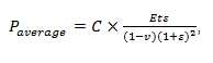
여기서 각각 t는 막의 두께이고, E 및 v는 각각 유효 영의 계수이고 및 푸아송의 비이다. 상수 C는 심장 크기가 증가할 때 감소하고, 및 C는 또한 심장의 모양(래빗 심장에 대하여 ~0.2 mm- 1)에 의존적이다. 막 두께 및 영의 계수 둘 모두에서 감소는 비례적으로 압력은 감소한다. 이러한 측정은 센서/작동기 네트워크 및 심외막 표면 사이의 우수한 접촉을 유지할 만큼 충분히 큰 압력을 제공하나, 본연의 생리상에 영향을 주는 것을 피할 만큼의 충분히 작은 압력을 제공하는 압력을 제공하는 설계를 가능하게 한다. 격리 압력상기 인가된 3D-MIM 유무에 따른 작동 래빗 심장 모델에 허혈을 나타내는 몇몇 전기 생리학적 파라미터의 시간 경과에 따른 모니터링은 효과가 있는 것으로 나타난다. 대조(N=3) 및 실험(N=3) 심장(도 8A 및 8B)에 기초한 결과는, ST 증폭 및 LV 압력 파형의 진폭에 의해 측정된 바와 같이, 상기 장치에 의해 유발되는 추가적인 허혈상기 없음을 나타냈다.Where t is the thickness of the film, E and v are respectively the effective zero coefficients and Poisson's ratio. Constant C is reduced when the size of the heart increased, and C is also (~ 0.2 mm with respect to the rabbit heart-1) shape of the heart it is dependent on. The decrease in both the film thickness and the coefficient of the Young's modulus decreases proportionally. These measurements provide a design that provides a pressure that is large enough to maintain good contact between the sensor / actuator network and the epicardial membrane surface, but that provides a pressure that is small enough to avoid affecting the natural physiological phase . Isolation pressure Over time monitoring of several electrophysiological parameters indicative of ischemia in the working rabbit heart model with and without the applied 3D-MIM appears to be effective. The results based on the control (N = 3) and experiment (N = 3) hearts (Figures 8A and 8B) show that additional ischemia induced by the device, as measured by the amplitude of the ST amplification and LV pressure waveform, Respectively.
작동의 다양한 기능적 모드를 설명하기 위해 우리는 심외막 전기 활성의 고정밀 맵핑을 수행한다. 상기 실험은, 및 하기의 모든 실험에서, 외식된 랑겐돌프-관류 래빗 심장을 사용하였다. 여기서 장치는 68 금 전극(1 mm2 표면적 및 3.5 mm의 간격)을 사용하였고, 심외막의 전 및 후 표면 둘 모두에 걸쳐 분포되었다(도 4A, 도4D, 도 9). 각각의 전극의 전기 화학적 임피던스는 1 kHz의 주파수에서 ~2 kΩ이고, 인산염 완충 염수에서 측정되었다(도 10). 막의 투명도는, 전기적 측정을 검증하기 위한 수단으로, 형광에 따른 전압을 통해 동시적인 광학 맵핑을 가능하게 한다.To illustrate the various functional modes of operation, we perform high-precision mapping of epicardial electroactivity. In this experiment, and in all of the following experiments, outpatient Langerden-perfused rabbit hearts were used. The device used 68 gold electrodes (1 mm2 surface area and 3.5 mm gap) and was distributed over both the anterior and posterior surfaces of the epicardium (Figs. 4A, 4D, Fig. 9). The electrochemical impedance of each electrode was ~ 2 kΩ at a frequency of 1 kHz and was measured in phosphate buffered saline (Figure 10). The transparency of the film enables simultaneous optical mapping through the voltage according to fluorescence as a means for verifying electrical measurements.
다양한 조건에서 4개의 심장으로부터 수득된 신호와 관련된 실험: 공간적 활성 맵에 프로파게이션 패턴의 변동성을 증가시키는 전극 쌍의 범위로부터 및 주파수의 범위에서 진행, 및 정상 시너스 리듬. 표면 전기기록도는 QRS 및 T 파형과 연관된 다양한 주요 형상을 포착하였다. 전기적 및 광학적 활성 시간 사이의 대표적인 맵 및 상호관계는 각각 도 4C 및 4B에 나타내었다. 광학적 및 전기적 활성 시간 사이의 전체적인 선형의 상호관계는 시너스 데이터로 0.957 및 보측된(paced) 데이터로 0.943 이었다. 상기 연구는 측정 전극의 상기 배열은 광학적으로 관찰된 공간적 변화를 포착하는 해상도로 활설화의 패턴을 복제할 수 있다. 추가적인 전기 생리학적 파라미터 분석은 도 12A, 12B 및 12C에 요약되었다. 도 4D는 심장의 전 및 후 표면 둘 모두로부터 기록된 신호로부터 유도된 3D 맵을 나타낸다. 모션 아티팩트가 극적으로 측정 품질에 영향을 주고 및 정적 심장 구조가 요구되는 광학 맵핑과 다르게, 3D-MIM으로 전기 생리적 맵핑은 정상 맥박 조건에서 적용될 수 있다. 통합된 센서는 아래에 위치하는 심장 조직과 동시적으로 움직이는 것으로 관찰되었다. 비록 맥박 주기 중 센서 및 심외막 사이의 상대적인 횡운동을 피하는 것은 부분적으로 어렵지만, 3D-MIM의 가공된 기하구조로 인해, 변위는 센서의 특징적인 크기보다 작게, 신호 품질에 무시해도 좋은 영향을 갖도록 최소화될 수 있다(도 11A, 11B, 및 11C). 상기 특징은 실험적 연구를 넘어서 맵핑 기능을 확장하고 임상의 전기 생리학에서 시행하는데 있어 중요하다.Experiments involving signals obtained from four hearts at various conditions: progression from a range of electrode pairs and from a range of frequencies, which increases the variability of the propagation pattern on the spatial activity map, and the normal sinus rhythm. Surface electrograms captured various key shapes associated with QRS and T waveforms. Representative maps and correlations between electrical and optical activation times are shown in Figures 4C and 4B, respectively. The overall linear correlation between optical and electrical activation times was 0.957 for the synapse data and 0.943 for the paced data. Such studies can replicate the pattern of activity at a resolution that captures the optically observed spatial variation of the measurement electrode. Additional electrophysiological parameter analysis is summarized in Figures 12A, 12B and 12C. 4D shows a 3D map derived from a recorded signal from both the front and the back surfaces of the heart. Unlike optical mapping, where motion artifacts dramatically affect the quality of measurement and static heart structures are required, electro-physiological mapping to 3D-MIM can be applied at normal pulse conditions. The integrated sensor was observed to move simultaneously with underlying cardiac tissue. Although it is partly difficult to avoid relative transverse motion between the sensor and the epicardium during the pulse period, due to the processed geometry of the 3D-MIM, the displacement must be smaller than the characteristic size of the sensor and negligible (Figs. 11A, 11B, and 11C). This feature is important beyond the experimental work to extend the mapping function and to implement it in clinical electrophysiology.
pH 변화의 맵핑은 심장의 대사 상태에 대한 유용한 정보를 제공한다. 여기서, 이리듐 산화물(IrOx), pH 센싱을 위해 잘 확립된 재료,는 상기 측정을 가능하게 한다. 금 전극에 전착된 IrOx는 타이로드 용액, 37℃에서 68.9 ± 8.6 mV/pH의 개방 회로 전위(OCP) 반응으로 pH 센서를 제공한다(도 13). 광학 맵핑 기술에 따른, 상기와 같은 pH 센서는 전체적인 무흐름 허혈-재관류 중에 pH 맵, 막투과 전위(Vm), 및 칼슘 과도(CaT) 신호의 수득을 가능하게 한다. 상기 pH 센서는 래빗 심장의 왼쪽 전면 및 후면을 덮는다(도 5A). 베이스라인에서, 모든 pH 센서는 7.34 내지 7.40의 값을 기록한다. 두개의 pH 센서(회색 및 차콜 색으로 표시됨)의 반응은 상기 프로토콜을 통해 도시되었다(도 5B). 시점 t1(베이스라인), t2(허혈 10분), 및 t3(재관류 20분)에서의 완전한 공간적 pH 맵을 도 5D-5E(왼쪽)에 나타내었다. 관류 펌프를 끄는 것은 즉각적으로 관상 압력을 0 mm Hg로 감소시키고 6.04(회색) 및 6.22(차콜)의 최소값의 pH로 대략적인 선형 감소를 야기한다. 재관류 상에, pH는 심실 빈맥(VT)의 시작까지 빠르게 증가하였고, 여기서 상기 pH는 베이스라인 값 아래의 수준에서 안정화된다. 재관류-유도된 VT의 샘플 원방 ECG는 도 5C에 나타내었다. 시너스 리듬으로 자발적인 전환 후, pH 값은 전 허혈 값으로 다시 증가한다. 도 5D-5F는 70%의 재분극(APD70)에서 pH 맵(왼쪽), 대표적인 광학 신호(Vm-흑색 및 CaT-회색; 중간) 및 나란히 활동 전위 지속 및 베이스라인으로 70%의 복원에서 칼슘 과도 지속(CaT70) 맵을 나타낸다. 베이스 라인에서, pH, APD70 및 CaT70 맵은 처음에 심장의 표면 상에 균일하였다. 10분의 허혈 후, pH, APD70, CaT70은 공간적으로 균일하지 않은 방법을 통해, 변화하였다. 20분의 재관류 후, 파라미터는 베이스 라인 수준에 근접한 수치로 변화하였다. 상기 실험은 허혈/재관류 중 다중파라미터 맵핑에 가능성을 설명한다. 상기 정보는 대사 및 흥분 수축 결합 사이의 해부학적 관계를 평가한다.The mapping of pH changes provides useful information about the metabolic state of the heart. Here, iridium oxide (IrO x ), a well established material for pH sensing, makes this measurement possible. The IrO x electrodeposited on the gold electrode provides a pH sensor with a tie-rod solution, an open circuit potential (OCP) reaction of 68.9 ± 8.6 mV / pH at 37 ° C. (FIG. 13). Such a pH sensor, in accordance with optical mapping techniques, enables the acquisition of a pH map, membrane permeation potential (Vm), and calcium transient (CaT) signal during global flow-free ischemia-reperfusion. The pH sensor covers the left front and back surfaces of the rabbit heart (Fig. 5A). At the baseline, all pH sensors record values from 7.34 to 7.40. The reaction of two pH sensors (shown in gray and charcoal) was shown via the protocol (Fig. 5B). A complete spatial pH map at time t 1 (baseline), t 2 (
온도 센서의 어레이와 3D-MIM은 심장 온도의 공간적 분포를 모니터링 기능을 수행한다. 상기 온도 센서 소자는 종래의 설계를 사용하고, 구불구불한 금 도관으로 구성되고(20μm 폭, 50 nm 두께)(도 14) 이것은 온도에 변화에 관계되어 저항상기 변화한다. 상기 온도 센서는 생물학적 범위 상에 비례적인 반응을 나타내는데, 전형적인 병원 설정인 2 Hz에서 샘플링할 때, ~23 mK의 측정 정확성을 가진다. 도 6A는 맥박하는 심장 상에 사용 중 16 통합 온도 센서와 3D-MIM을 나타낸다. 상기 센서는 동물 실험 전에 온도 조절 수조에서 교정되고, 어레이를 가로지르는 16 센서 상에 1.23 ± 0.05 Ω/℃의 반응을 보였다(도 15). 한 실시예로, 심장의 온도는 관류의 온도를 변경함으로써 변화하였다. 도 6A에 나타난 바와 같이, 측정된 심외막 온도는 심장에 걸친 온도의 균일한 분산과 관류의 냉각시, 점차적으로 ~7℃ 까지 감소하였다. 원방 전자 곡선으로부터 결정된, 심박수는 온도의 감소와 함께 감소되고 온도가 생물학적 수준으로 회복함에 따라 원래의 값으로 복원된다. 이것은 온도가 심근 대사의 속도를 조절한다는 것을 말한다. 두번째 실험에서, 카우테리 펜상기 심막의 작은 영역을 극히 태우는데 사용되었다. 관련 온도 맵(도 6B)상기 절제의 부분 근처의 온도의 국소된 상승을 나타낸다. 상기와 같은 정보는 영향을 받은 영역의 크기 및 절제 시간의 임상적 조절의 피드백으로서 사용될 수 있다. 전기 센서와 조합하여, 상기와 같은 장치는 실시간으로 온도 및 흥분 사이의 관계를 제공한다.The array of temperature sensors and 3D-MIM monitor the spatial distribution of heart temperature. The temperature sensor element uses a conventional design and consists of a twisted gold conduit (20 [mu] m wide, 50 nm thick) (Fig. 14) which changes in resistance with respect to changes in temperature. The temperature sensor exhibits a proportional response over the biological range, which has a measurement accuracy of ~ 23 mK when sampling at a typical hospital setting of 2 Hz. 6A shows 16 integrated temperature sensors and 3D-MIM in use on a pulsating heart. The sensor was calibrated in a temperature-controlled bath prior to animal testing and showed a response of 1.23 +/- 0.05? / ° C on 16 sensors across the array (Fig. 15). In one embodiment, the temperature of the heart has changed by changing the temperature of the perfusion. As shown in Figure 6A, the measured epicardial membrane temperature gradually decreased to ~ 7 ° C during the cooling of the perfusion and the even distribution of temperature across the heart. The heart rate, determined from the far-field electron curves, decreases with decreasing temperature and is restored to its original value as the temperature returns to the biological level. This means that temperature controls the rate of myocardial metabolism. In a second experiment, cautery pen was used to scavenge a small area of the pericardium. The associated temperature map (Figure 6B) shows a localized rise in temperature near the portion of the ablation. Such information can be used as a feedback on the clinical adjustment of the size of the affected area and resection time. In combination with an electrical sensor, such a device provides a real-time relationship between temperature and excitation.
전기적 및 화학적 평과 외에도, 기계적 특성상기 판단될 수 있다. 여기서, Si의 나노막에 압저항 효과에 기초한 변형률 센서는 다양한 전파 상태 중 심장의 수축의 기계적 특징을 모니터링할 수 있게 한다. 구불구불한 연결부 구조의 주의 깊은 기계 설계는 이전에 보고된 소규모 2D 장치의 설명과 같이, 전형적인 심외막 변형률은 Si의 파괴 임계 값을 초과한다는 사실에도 불구하고 정확한 측정을 가능하게 한다. 본 설계에 있어서, 3D MIM 스트레인(변형률) 센서는 로젯형의(도. 16a 및도 16b) 세 개의 p- 도핑 실리콘 압저항 소자를 포함한다. 각 압 저항에 대해 ~ -0.06의 ~ 0.33 효과적인 가로 게이지 요소의 효과적인 길상기 게이지 계수를 제공하고 서로의 상기 Si의 <110> 결정질 방향으로 정렬됩니다(도17). 다른 피에조 저항은 <100> 결정 배향 방향에 의한 결정 방향뿐만 아니라, 장치 전체의 형상과 관련된 극한 감도로 변형 하에서 저항상기 상대적으로 작은 변화를 나타내고 있다. <100> 방향으로 정렬된 압 저항 온도의 효과를 보정 하는데 사용할 수 있는 반면 <110> 방향으로 정렬된 압 저항은 심장의 기계적 리듬의 특성에 대한 최대 감도를 제공한다. 실험은 시너스 리듬, 심실 조율, 및 피나시딜과 약리학적으로 유도된 심실 세동(VF) 동안의 기계적인 거동을 규명하였습니다. 배쓰(bath) 전극은 전기 및 기계 행동 사이의 시간적 상관관계를 설정하기 위해 원방 ECG의 동시적인 기록을 가능하게 했다. 도 6c는 <110> 방향으로 정렬 대표적인 압 저항 소자의 반응을 나타낸다. 측정은 ECG 기록과 일치하는 타이밍과 상기 심장 주기의 기계적 리듬을 보여준다. VF 조건에서, 스트레인 게이지 및 ECG 모두 파형상기 정상 리듬을 잃고 VF의 일반적인 임의의 패턴을 표시 것으로 나타났다.In addition to electrical and chemical evaluation, the mechanical properties can be judged as above. Here, a strain sensor based on the piezoresistive effect on the Si nanofilm allows monitoring of mechanical characteristics of contraction of the heart among various propagation states. Careful mechanical design of the twisted joint structure allows accurate measurement, despite the fact that typical epicardial strain exceeds the Si breakdown threshold, as described in the previously reported small 2D devices. In this design, the 3D MIM strain (strain) sensor includes three p-doped silicon piezoresistive elements of the rosette type (Figs. 16a and 16b). The effective lateral gauge factor of -0.06 to -0.33 effective transverse gauge elements for each piezoresist is provided and aligned with the <110> crystalline orientation of the Si of each other (FIG. 17). The other piezoresistors exhibit a relatively small change in resistivity under the strain, not only in the crystal orientation by the <100> crystal orientation direction, but also in the extreme sensitivity associated with the shape of the entire device. Resistance aligned in the <100> direction can be used to compensate for the effect of piezoresistive temperature, while piezoresistance aligned in the <110> direction provides maximum sensitivity to the characteristics of the mechanical rhythm of the heart. The experiment identified synergistic rhythm, ventricular tachycardia, and mechanical behavior during pinacidil and pharmacologically induced ventricular fibrillation (VF). The bath electrode enabled simultaneous recording of the far field ECG to establish a temporal correlation between electrical and mechanical behavior. FIG. 6C shows a typical response of the piezoresistive element aligned in the <110> direction. The measurements show the timing corresponding to the ECG record and the mechanical rhythm of the cardiac cycle. Under VF conditions, both the strain gage and the ECG showed that the waveform loses the normal rhythm described above and displays a common random pattern of VF.
최종 설명은 첨단 반도체 통합 및 광학 맵핑/자극을 위한 기능을 설명하기 위해, μ-ILED의 어레이를 이용한다. 여기서는, 670 nm의 피크 방출 파장과 알루미늄 갈륨 인듐 인화물(AlInGaP)에 기초하여 9개의 초박막(3 μm), 마이크로크기(300x300 μm2) 발광 다이오드(LED)가 (도. 18.도 19A, 19B 및 19C) 전압에 민감한 염료의 여기를 위한 국소 광원이다. 이러한 염료와 관련된 형광의 변화는 심장의 활동 전위의 측정을 허용한다. 도 6D는 외부 광원(Prizmatix, 630 ㎚)와 통합 μ-ILEDs로 얻은 신호를 비교한다. 그들의 작은 크기에도, LED는, 외광과 일치하는 파형 모양으로, 분명한 활동 전위의 기록을 가능하게 한다. 결과는 3D 적분 형식의 생체 내 광학 매핑 및/또는 자극 시스템의 가능성을 증명한다.The final description uses an array of μ-ILEDs to illustrate advanced semiconductor integration and functions for optical mapping / stimulation. Here, nine ultra-thin (3 μm), micro-sized (300 × 300 μm 2 ) light emitting diodes (LEDs) based on the peak emission wavelength of 670 nm and aluminum gallium indium phosphide (AlInGaP) 19C) is a local light source for excitation of voltage sensitive dyes. Fluorescence changes associated with these dyes allow the measurement of the action potential of the heart. Figure 6D compares signals obtained with an external light source (Prizmatix, 630 nm) and integrated μ-ILEDs. Even in their small size, LEDs enable the recording of a clear action potential, in the shape of a waveform that matches the ambient light. The results demonstrate the possibility of in vivo optical mapping and / or stimulation systems in 3D integral form.
상기 예에서 설명된 결과는 생물의학 연구 및 임상 애플리케이션 모두에서 잠재적인 활용과, 3D, 장기-특정 설계에서, 활성 전자 재료 및 센서를 인터페이스하기 위한 경로를 제시한다. 재료, 공학 역학 및 기능적 장치에 대한 관심과, 이러한 시스템은 심장 외막에 등각 인터페이스를 구축하고, 다양한 고밀도, 큰 면적 생리학적 다중 파라미터의 매핑 및 자극을 수행할 수 있다. 상기 장치는 다양한 인설트(insult), 질병 및 치료의 공간적 시간적 반응을 모두에 대한 조사를 위한 대사적, 흥분, 이온, 수축, 열 상태에 대한 국소 정보를 제공할 수 있습니다. 상기 장치는 부정맥, 허혈, 저산소증, 절제 인한 외상이나 심부전 같은 병태 생리학적 상태의 출처를 나타내는 중요한 영역을 식별하기 위해 사용될 수 있다. 상기 영역은 다음 치료 개입을 유도하는데 사용될 수 있다. 이러한 접근 방법은 진단 및 치명적인 심장 질환의 치료를 위한 고해상도 이식 장치를 설계하고 구현하는 유망한 기회를 제시한다.The results described in the above examples present potential applications in both biomedical research and clinical applications and paths for interfacing active electronic materials and sensors in 3D, organ-specific designs. With interest in materials, engineering dynamics, and functional devices, such systems can build conformal interfaces to the epicardium and perform mapping and stimulation of various high density, large area physiological multiple parameters. The device can provide local information on metabolic, excitability, ionic, shrinkage, and thermal conditions for investigation of various insults, both spatial and temporal responses of disease and treatment. The device can be used to identify critical areas that indicate the origin of pathophysiological conditions such as arrhythmia, ischemia, hypoxia, ablative trauma or heart failure. The region may be used to induce the next therapeutic intervention. This approach presents a promising opportunity to design and implement high-resolution implant devices for diagnosis and treatment of fatal heart disease.
방법Way
3D-MIM의 제작: 아래 설명된, 공정은 폴리(메틸 메타아크릴레이트)(PMMA) 상의 폴리이미드(PI)의 이중층과 또는 폴리(디메틸실록산)(PDMS) 상의 폴리(에틸렌 테레프탈레이트)(PET)로 코팅된 기판상에 전사 인쇄한 다음, 무기 반도체 재료 (실리콘, InGaN 또는 AlInGaP)의 기준 평면 가공을 시작한다. PMMA의 용해 또는 PDMS로부터 박리로 장치의 해제를 할 수 있습니다. 금속층(Cr/금)은 진공 증착 및 인터커넥트 저항 및 전극을 형성하도록 패터닝된다. 장치의 상부에 폴리머 밀봉 층(PI 또는 감광성 에폭시 SU8)의 적용 및 패터닝은 제조를 완료시킨다. 전사 인쇄는 낮은 모듈러스 실리콘 탄성 중합체의 박막으로 얻어진 구조를 제공한다(Ecoflex, Smooth-on). 주변에 접촉 패드에 결합된 유연한 전도성 케이블(Elform)은 외부 하드웨어에 대한 인터페이스를 제공합니다. 적층 공정은 표면과 직접 접촉 센서, 심장의 원하는 3D 인쇄 모델 장치를 첨부. 주조 및 엘라스토머 같은 다른 유형의 층을 경화하는 것상기 시스템의 전체 3D 형상을 정의한다. 일부의 경우, 엘라스토머 스트랩 랑겐 돌프 관류 심장 실험에 사용하기 위한 기동력 (도. 20)를 강화한다. 멤브레인에 추가의 개구부는 지지 수조에 흐름과 연관된 유체 축적을 방지하기 위해 포함될 수 있다. 모델로부터 제거는 IrOx의 전착을 가능하게 하고 정밀 pH를 감지를위한 깨끗한 표면을 얻을 수 있습니다. Fabrication of 3D-MIM: The process, described below, can be performed with a double layer of polyimide (PI) on poly (methyl methacrylate) (PMMA) or with a double layer of poly (ethylene terephthalate) (PET) on poly (dimethylsiloxane) And the reference plane processing of the inorganic semiconductor material (silicon, InGaN or AlInGaP) is started. The device can be released by dissolving PMMA or peeling from PDMS. The metal layer (Cr / gold) is patterned to form vacuum deposition and interconnect resistance and electrodes. Application and patterning of the polymer sealing layer (PI or photosensitive epoxy SU8) on top of the device completes the manufacturing. Transfer printing provides a structure obtained from a thin film of low modulus silicone elastomer (Ecoflex, Smooth-on). A flexible conductive cable (Elform) attached to the surrounding contact pads provides an interface to external hardware. The laminating process attaches to the desired 3D printing model device of the heart, the sensor directly touching the surface. Casting and curing of other types of layers such as elastomers defines the overall 3D shape of the system. In some cases, strengthening the maneuver force (Fig. 20) for use in elastomeric strap Langendorff perfusion heart trials. Additional openings in the membrane may be included to prevent fluid accumulation associated with flow in the support bath. Removal from the model enables the deposition of IrO x and provides a clean surface for accurate pH detection.
동물 실험 : 실험은 세인트 루이스의 워싱턴 대학의 기관 동물 관리 및 사용위원회의 승인과 국립 연구소의 윤리적 지침에 따라 실시하였다. 이전 문헌에 보고 랑겐돌프 관류 래빗 심장 상의 광 매핑 절차를 수행하였다. 도 21은 대표적인 실험적인 설정을 나타낸다. 간단히 심장은 개흉술을 통해 제거되고 정맥은 산소 타이로드의 솔루션의 역 행성 관류를 허용하도록 대동맥에 배치됩니다. 관류 동물 내의 전해질 균형을 모방하고 심장의 전기적 관점에서 정상적으로 작동을 계속하기 위해 에너지 기판을 제공한다. 심장은 37℃에서 7.4 ± 0.05의 pH로 유지된 관류 챔버에 침수된다. 형광 전위차 염료로부터의 신호(di-4 ANEPPS 또는 RH-237) 또는 칼슘 인디케이터(Rhod-2a)의 수집에 의존하는 트랜스 전위(VM)와 칼슘 과도(CAT)의 광신호는 관류 액에 CMOS 카메라와 첨가되고; 모션 아티팩트를 피하기 위해 필요할 때, 여기 수축 비-짝지음(Blebbistatin)도 관류 액에 첨가된다.Animal Testing: The experiment was conducted in accordance with the Ethical Guidelines of the National Institutes of Education and the approval of the Institutional Animal Care and Use Committee of the University of Washington in St. Louis. In previous literature, a light mapping procedure was performed on the Rangendorf perfused rabbit heart. Figure 21 shows a representative experimental setting. Briefly the heart is removed through thoracotomy and the vein is placed in the aorta to allow retrograde perfusion of a solution of oxygen tie rod. Imitates the electrolyte balance in the perfusion animal and provides an energy substrate for continuing normal operation from the electrical point of view of the heart. The heart is submerged in a perfusion chamber maintained at a pH of 7.4 +/- 0.05 at 37 < 0 > C. The transient potential (VM) and calcium transient (CAT) optical signals, which are dependent on the collection of signals from fluorescent potential dye (di-4 ANEPPS or RH-237) or calcium indicator (Rhod- Added; When necessary to avoid motion artifacts, excitation non-paired (Blebbistatin) is also added to the perfusion solution.
데이터 수집 및 처리Data collection and processing
1. 전기 생리학 : 전기 신호는 240-채널 단극 전기도 수집 시스템 (Astrocard, 보스턴)와 맞춤형 인터페이스와 3D-MIM에 금 전극에서 기록된다. 두 광 및 전기 신호를 트리거 TTL 펄스 및 사후 처리 맞춤 MATLAB 소프트웨어 개별적으로 정렬된 1 kHz의 샘플링 주파수로 수집된다. 후 처리: 입체 · 개의 MIM로부터 취득한 전기 신호는 먼저 수집 소프트웨어 후 관심 활성화 시간의 전기 생리 학적 파라미터가 산출된다 (.도 4C) 내부의 60 Hz에서의 노치 필터로 여과하고, 공간적 좌표로 정렬 광 배경 파일에 기초하여 상기 전극. 광 신호를 여과하고, 정규화 비닝된다. 전기 생리 매개 변수는보기의 전체 필드에 대해 계산됩니다. 공간맵를 만들려면, 활성화 시간은 흩어져있는 데이터의 차 보간을위한 MATLAB의 내부 기능을 사용하여 보간된다. 광 맵은 또한 전극의 좌표로 샘플링되고, 동일한 보간 방법은 샘플링된 광맵 및 전기맵 전체 해상도 광 패턴을 비교하기 위해 적용된다.1. Electrophysiology: Electrical signals are recorded on a gold electrode in a 240-channel unipolar electrical collection system (Astrocard, Boston) and a custom interface and 3D-MIM. Triggering both optical and electrical signals TTL pulses and post-processing Custom MATLAB software is collected at individually sampled 1 kHz sampling frequency. Postprocessing: The electrical signals obtained from the stereomorphic MIMs are first filtered by an internal 60 Hz notch filter, and then arranged in spatial coordinates (Figure 4C). The electrophysiological parameters of the activation time of interest after the acquisition software are calculated Based on the file. The optical signal is filtered and normalized and binned. The electrophysiological parameters are calculated for the entire field of view. To create a spatial map, the activation time is interpolated using MATLAB's internal functions for interpolating scattered data. The light map is also sampled at the coordinates of the electrodes, and the same interpolation method is applied to compare the sampled light map and the electric map full resolution light pattern.
2. 산도는 데이터의 Ag / AgCl을 전극에 참조된 각 센서의 개방 회로 전위를 측정하여 획득된다.2. The acidity is obtained by measuring the open circuit potential of each sensor referenced to the Ag / AgCl electrode.
3. 온도와 스트레인 센서 데이터는 내쇼날 인스트루먼트의 PXI-6289 보드를 기반으로 사용자 정의 내장된 시스템을 사용하여 각 센서의 저항 측정을 취득된다.3. Temperature and strain sensor data is acquired using a custom built-in system based on the National Instruments PXI-6289 board to measure the resistance of each sensor.
그림 설명Picture description
도. 2A, 2B와 2C : 전체 심 외막 표면을 가로 질러 시공간 측정 / 자극 3D 다기능 외피 막 (3D-개의 MIM). 도. 2A : 장치의 설계 및 제조의 주요 단계의 그래픽 묘사. 스케일 바 : 2cm. 도. (b) : 대표적인 3D-MIM의 이미지는 랑겐 돌프 - 관류 래빗 심장에 통합. 흰색 화살표는 상기 시스템의 다양한 기능 요소를 강조 표시합니다. 전자는 심장 (삽입) 모두 전방 및 후방 표면을 커버 할 수 있다. 스케일 바 : 6mm. 도. 2C는 : 심장 외막에 등각 접촉하는 기능 요소의 전망을 확대. 이미지는 장치의 배면 측으로부터 기록된다. 스케일 바 : 500 μm.Degree. 2A, 2B and 2C: Spatio-temporal measurement / stimulation across the entire epicardial surface. 3D multifunctional envelope membrane (3D-MIM). Degree. 2A: A graphic depiction of the main stages of the design and manufacture of the device. Scale bar: 2cm. Degree. (b): The image of a typical 3D-MIM is integrated into the Languedoc-Rabbit heart. A white arrow highlights the various functional elements of the system. The former can cover both the anterior and posterior surfaces of the heart (insertion). Scale bar: 6mm. Degree. 2C: Enlarge the prospect of functional elements that conform to the epicardium conformally. The image is recorded from the back side of the apparatus. Scale bar: 500 μm.
도. 3A 및 3B : 3 D-MIM의 통합과 관련된 심장 외막에 압력 분석. 도 3A : 총 150 μm의 두께와 심장의 구조의 부피 팽창의 다양한 조건에서 60 kPa의 유효 탄성 계수를 가진 장치에 의한 계산된 압력 분포. 도. 3B : FEM 및 부피 팽창 (왼쪽), 두께 (중간) 및 멤브레인의 영률(영의 계수) (우)의 함수로서 평균 압력의 분석 결과.Degree. 3A and 3B: Pressure analysis on the epicardium associated with the integration of 3 D-MIM. Figure 3A: Calculated pressure distribution by a device with effective elastic modulus of 60 kPa under various conditions of total thickness of 150 μm and volume expansion of the structure of the heart. Degree. 3B: Analysis of mean pressure as a function of FEM and volume expansion (left), thickness (middle) and Young's modulus (zero coefficient) of the membrane (right).
도. 도 4A, 4B, 4C 및 4D : 고밀도 전기 매핑 도. 4A 랑겐 돌프 - 관류 래빗 심장에 해당하는 색깔의 전극 위치에서 동시에 획득한 대표적인 광학 및 전기 신호. 스케일 바 : 7mm. 도. (b) : 최고 : 대표적인 광학 활동 전위 (OAP)의 개략도, 단극 전기도 (EG)와 의 OAP에 대해 dV/dtMax로 및 EG에 대해 -dV/dtMax로 정의 활성화 시간, 위치: 다양한 테스트 심장 전기 및 광학 활성 시간의 상관관계. 도. 4C : 전기 및 광학 측정에서 결정 보간 공간 활성 맵. 위 : 막에 전극의 빨간 쌍에 의해 진행된 심장, 바닥 : 동 리듬. 도. 4D : 심장의 전방 및 후방 표면 모두에서 전기 신호의 3D 매핑. 전기적 활성화 시간의 공간 보간 맵 시각화 목적 대표적인 래빗 심장 형상에 투영된다. 스케일 바 : 7mm.Degree. 4A, 4B, 4C and 4D: high density electrical mapping diagram. 4A Langendorff - Perfusion Rabbit Representative optical and electrical signals acquired simultaneously on colored electrodes corresponding to the heart. Scale bar: 7mm. Degree. (b): Schematic of representative optical activity potential (OAP), defined as dV / dt Max for OAP with unipolar electrical diagram (EG) and -dV / dt Max for EG Activation time, location: Correlation of cardiac electrical and optical activity time. Degree. 4C: Decision interpolation space active map in electrical and optical measurements. Above: the heart, the bottom, proceeded by a red pair of electrodes on the membrane: rhythm. Degree. 4D: 3D mapping of electrical signals on both the anterior and posterior surfaces of the heart. Spatial interpolation map of electrical activation time is projected onto a typical rabbit heart shape for visualization purposes. Scale bar: 7mm.
도 5A, 5B, 5C, 5D, 5E 및 5F : 트랜스 전위 칼슘 과도 동시에 광학적 맵핑 고밀도 산도 매핑 도. 5A : 3D-MIM상기 pH 센서와 랑겐 돌프 관류 래빗 심장 집적적인 pH 센서 어레이와 함께 값도 표시. 5B. 스케일 바 : 7mm. 도. 5B : 재관류 30 분 뒤에 비-흐름 허혈 30분 동안 pH의 시간적 변화. 세 시간은 T1, T2, 및 T3는 도에서 공간의 pH 맵에 해당 5D-5F. 도. 5C : 기준 및 재관류에 의한 VT 동안 대표적인 원방 ECG. 도. 베이스 라인에서 32 센서 (왼쪽), 대표적인 횡단 전위와 칼슘 과도 신호 (가운데)의 pH를 맵핑하고, APD70-CaT70 맵 (오른쪽) (도 5D.), 노-흐름 허혈 10분 (도 : 5D-5F. 5E) 및 재관류 20분 (.도 5F). VT, 심실 빈맥; VM, 횡단 전위; CAT, 칼슘 과도; APD70, 70 % 재분극에서 활동 전위 기간; CaT70, 70 % 완화에서 칼슘 과도 기간입니다. 5A, 5B, 5C, 5D, 5E and 5F: optical mapping high density acidity mapping simultaneously with transposition calcium. 5A: 3D-MIM The value is displayed with the pH sensor and Rangendorf perfusion rabbit heart-integrated pH sensor array. 5B. Scale bar: 7mm. Degree. 5B:
도 6A, 6B, 6C 및 6D : 고밀도 온도 및 변형률 탐지 및 이미징 μ-ILEDs 통합 사용. 도. 6A : 냉각 관류하는 동안 온도 모니터링을 위한 3D-MIM의 응용 프로그램. 왼쪽: 랑겐 돌프 - 관류 래빗 심장에 통합된 4 × 4 온도 센서 어레이와 3D-MIM의 이미지입니다. 중간: 왼쪽 삽입에 도시된 대표적인 센서의 온도 기록. 오른쪽 : ECG에서 계산된 해당 심박수와 중간 삽입 대표적인 시점에서 온도 맵. 컬러 맵의 각 픽셀은 하나의 온도 센서로부터의 기록에 대응한다. 스케일 바 : 1cm. 도. 6B : 절제 실험동안 온도 측정. 상기 센서 어레이와 소작 펜의 위치가 왼쪽 삽입에 나타낸다. 대표적인 센서 (오른쪽 아래)에서 제거 (오른쪽)과 녹음하는 동안 온도 맵은 각각 표시됩니다. 스케일 바 : 7mm. 도. 6C : ECG 동시 녹화 비해 대표적인 생리 조건하에서 실리콘 스트레인 센서의 응답. 도. 6D : 왼쪽 : 광학 매핑 실험에서 μ-ILEDs 배열과 3D-MIM의 이미지입니다. 삽입된 대표적인 μ-ILED 주변 영역의 확대도를 나타낸다. 오른쪽 : 각각 3D-MIM 및 외부 광 여기에 μ-ILED를 사용하여 여기 동안 기록된 대표적인 화소에서 광신호의 비교 (왼쪽 삽입에 파란색 점). 스케일 바 : 3mm.Figures 6A, 6B, 6C and 6D: High density temperature and strain detection and imaging using μ-ILEDs integrated. Degree. 6A: Application of 3D-MIM for temperature monitoring during cooling perfusion. Left: Langendorf - perfusion Rabbit An image of a 4 × 4 temperature sensor array and 3D-MIM integrated in the heart. Medium: Temperature record of the representative sensor shown in left insert. Right: Temperature map at the corresponding heart rate and median insertion at the calculated ECG. Each pixel of the color map corresponds to a record from one temperature sensor. Scale bar: 1cm. Degree. 6B: Temperature measurement during ablation experiments. The positions of the sensor array and the cauterization pen are shown in the left insert. The representative sensors (lower right) remove (right) and the temperature map during recording, respectively. Scale bar: 7mm. Degree. 6C: Response of silicon strain sensor under typical physiological conditions compared with ECG simultaneous recording. Degree. 6D: Left: Image of μ-ILEDs array and 3D-MIM in optical mapping experiment. And shows an enlarged view of a representative μ-ILED peripheral area inserted. Right: Comparison of optical signals (blue dot on the left insert) at representative pixels recorded during excitation using μ-ILED for 3D-MIM and external light excitation, respectively. Scale bar: 3mm.
3D-MIM의 역학 분석.Dynamic analysis of 3D-MIM.
IN. 3D FEM에 의한 수치 해석. 3D FEM은 3D 다기능 외피 막 (3D-MIM) 및 디바이스 파라미터의 넓은 범위의 심장과 심장의 확장 사이의 압력을 연구하는 데 사용됩니다. 심장의 3D 기하학적 모델은 의료 검사에서 얻어진 광학 세분화에 의해 재구성된다. 기하학적 모델은 ABAQUS 유한 요소 프로그램의 전처리로 가져옵니다. 심장과 3D-MIM은 각각 4 노드, 선형 사면체 솔리드 요소 C3D4와 ABAQUS의 4 노드 사변형 막 엘리먼트 M3D4에 의해 모델링된다. 요소의 전체 개수는 60,000을 초과하고, 정제가 수치 결과의 정확성을 보장 메쉬. 심장의 소정의 확장, FEM은 3D-MIM과 중심 사이의 계면에서의 압력 분포를 제공한다. 도 1에 도시된 바와 같이, 평균 압력은 상기 3D MIM 및 심장 실험에서와 같이, 즉 심장의 심실 사이의 접촉 면적을 통해 얻어진다. 도 3A. IN. Numerical Analysis by 3D FEM . 3D FEM is used to study the pressure between the heart and the expansion of the heart in a wide range of 3D multifunctional envelope membranes (3D-MIM) and device parameters. The 3D geometric model of the heart is reconstructed by optical segmentation obtained from a medical examination. Geometric models are imported into the ABAQUS finite element preprocessor. The heart and the 3D-MIM are modeled by four nodes, linear tetrahedral solid elements C3D4 and ABAQUS four-node quadrilateral membrane element M3D4, respectively. The total number of elements exceeds 60,000, and the refining mesh ensures the accuracy of the numerical results. A given extension of the heart, the FEM, provides a pressure distribution at the interface between the 3D-MIM and the center. As shown in FIG. 1, the mean pressure is obtained as in the 3D MIM and cardiac experiments, i. E. Through the contact area between the cardiac chambers. 3A.
II. 압력. 도에 도시된 바와 같상기 3D MIM (도. 3A)에 의해 피복되어 심장의 일부는 대략 길상기 A 및 반 - 주축의 B를 부분 선대칭 타원체이다. 도 7a 및 도 7b. 심장 표면의 3D-MIM은 막으로 제조되고, 심장의 선형 팽창 ε로 인해, z2/[(1+ε)2a2] + r2/[(1+ε)2b2] = 1 에 따라 제조될때, (Z, R) 및 (z,r) = [(1+ε)Z, (1+ε)R]은 각각 3D-MIM의 수직 및 라디칼 좌표이다. 3D-MIM의 평면 부하 상태는 이축성 선형 변화 ε은 이축성 부하 Eε/(1-ν)를 준다. 여기서, 각각 E 및 ν는 영률이고 및 푸이손의 비율이다. 막 힘, 선형 팽창으로 인한 길상기 변화의 계산은 II. pressure. As shown in the figure, a portion of the heart covered by the 3D MIM (Fig. 3A) is a partially symmetric ellipsoid A of about the length A and a B of the semi - major axis. 7A and 7B. The 3D-MIM of the heart surface is made of a membrane, and due to the linear expansion of the heart, z 2 / [(1 + ε) 2 a 2 ] + r 2 / [(1 + ε) 2 b 2 ] (Z, R) and (z, r) = [(1 + epsilon) Z, (1 + epsilon) R] are the vertical and radical coordinates of the 3D-MIM, respectively. The plane load condition of the 3D-MIM is given by the biaxial linear change ε given by the biaxial load Eε / (1-ν). Where E and v are the Young's moduli and the Poisson's ratio, respectively. The calculation of the change in the path due to membrane force, linear expansion
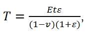
여기서, t는 3-D MIM의 두께이다. 평면 곡선 r = r(z)이고, 표면상의 임의의 점 (Z, R)에서 자오면 방향에 따른 주 곡률은-(dr2/dz2)/[1+(dr/dz)2]3 /2이다. 둘레방향에 따른 여타 주 곡률은 ![]()
![]()
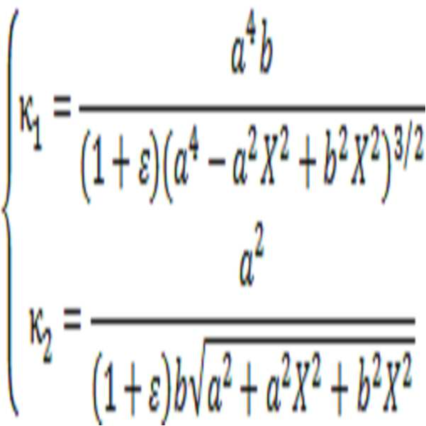
심장에 압력은 하기식과 같은 멤브레인 장력 곡률 등의 조건에서 얻어진다.The pressure on the heart is obtained under such conditions as membrane tension curvature such as the following equation.
![]()
![]()
심장과 접촉하는 하기 식의 타원체 표면의 (Z0 ≤ Z ≤ A,도. 7A)의 일부에 걸친 평균은 The average over a portion of the ellipsoidal surface of the following equation (Z0 ≤ Z ≤ A, Fig. 7A) in contact with the heart
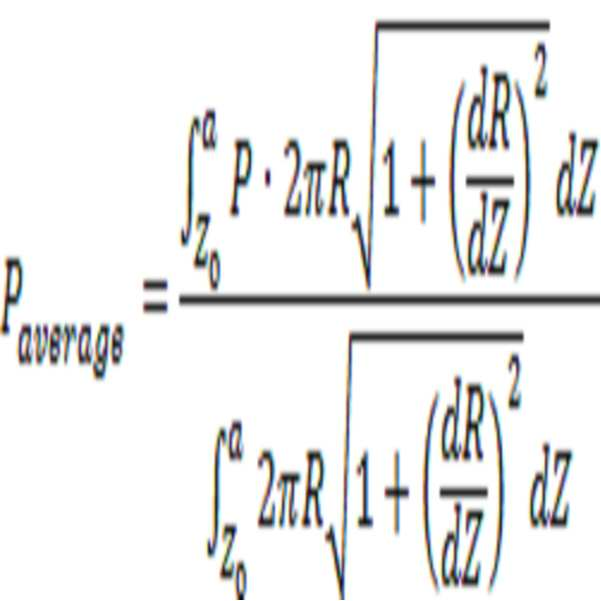
상기 식 및The above formula and
a = 15mm, b = 10 mm 0 X = -5.5 mm인 경우, 가장 심장의 기하학적 모델 식의 평균 압력에 알만다. 식 (1)가 3D-FEM 결과와 잘 일치한다. 도 3BIf a = 15 mm, b = 10 mm and 0 X = -5.5 mm, the mean pressure of the most geometric model equation of the heart is known. Equation (1) agrees well with 3D-FEM results. 3B
분석은 위의 3D-MIM와 심장 사이의 압력에 전자 장치의 효과를 고려하지 않습니다. 이러한 효과는 수학식으로부터 추정될 수있다. (1) 전자 장치와 3D MIM의 유효 인장 강성과 3D-MIM의 인장 강성을 잇 대체함으로써. 도 세트입니다. 도 7b는 배선 전극으로 이루어지는 멤브레인 재료 (62.8 X 24.3 X 0.15 MM3)의 시트 상에 전자 장치를 도시한다. 연결부는 모두 Au로 구성 : 120 ㎚ / CR : 1.2 μm의 두께의 폴리이미드 (PI)는 각 측의 층상기 끼워진 나노 복합 층. 전극의 단면은 커넥터와 유사하지만, Au로 노출되도록 상부 1.2 μm의 두께 PI 층없이. 시트는 8 노드 고체 소자 C3D8R 의해 모델링 되고, 배선 및 전극은 각각 ABAQUS의 4 노드 S4R 쉘 요소로 모델화된다. FEM은 인장 강도가 전자 장치 없이도 1에 나타낸 약 1.5 배로 준다. 7B.The analysis does not take into account the effect of electronic devices on the pressure between the above 3D-MIM and the heart. This effect can be estimated from the equation. (1) By replacing the effective tensile stiffness of the 3D MIM with the electronic device and the tensile stiffness of the 3D-MIM. It is also a set. Figure 7b shows an electronic device on a sheet of membrane material (62.8 X 24.3 X 0.15 MM3) consisting of wiring electrodes. The connections consist of all Au: 120 nm / CR: 1.2 μm thick polyimide (PI) layers on each side. The cross section of the electrode is similar to the connector, but without the upper 1.2 μm thick PI layer to be exposed to Au. The sheet is modeled by an 8-node solid state device, C3D8R, and the wires and electrodes are each modeled as a 4-node S4R shell element of ABAQUS. The FEM gives a tensile strength of about 1.5 times as shown in Fig. 7B.
3D-3D- MIM에 대한 제조 절차Manufacturing procedure for MIM
I. 도 2에 나타나는 다양한 전자 부품의 배열의 3D-MIM≪ RTI ID = 0.0 > I. < / RTI > 3D-MIM
실리콘 나노막의 p 형 도핑.P-type doping of silicon nanomaterials.
1. 아세톤 (150 nm의 매립 산화막에 320 nm의 실리콘) 인슐레이터 (SOI) 웨이퍼상의 실리콘, 이소 프로필 알콜 (IPA) 및 탈이온화수로 씻어주고, 5분 동안 110℃에서 탈수한다.1. Wash with silicon, isopropyl alcohol (IPA) and deionized water on an acetone (320 nm silicon on a 150 nm buried oxide) insulator (SOI) wafer and dehydrate at 110 ° C for 5 minutes.
2. 버퍼 산화물 에칭 (BOE) 6 : 1로 1분 동안 씻어 준다.2. Rinse buffer oxide etch (BOE) 6: 1 for 1 minute.
3. 10분 동안 1000℃에서 확산 붕소 원에 노출 시킨다.3. Expose the diffusion boron source at 1000 ° C for 10 minutes.
4. HF로 1분 동안 처리된 웨이퍼를 씻어주고, RCA1으로 10분, RCA2로 10분 및 BOE로 1분 씨어준다.4. Wash the wafers treated with HF for 1 minute, slaughter for 10 minutes with RCA1, 10 minutes with RCA2 and 1 minute with BOE.
InGaN μ-ILED의 준비.Preparation of InGaN μ-ILED.
5. 스핀 코팅과 포토 레지스트(PR) 패터닝(AZ 5214 E), 질화 갈륨 /시 (111) 에피 웨이퍼 (Azzurro Semiconductor, GaN: Mg (110 nm)//five repeats of InGaN (3 nm), GaN: Si (10 nm)//GaN: Si (1,700 nm)//AlN: Si/GaN: Si (1,900 nm)//GaN (750 nm)//AlN/AlGaN (300 nm)//Si (111)).5. Spin coating and photoresist (PR) patterning (AZ 5214 E), gallium nitride / Si (111) epitaxial wafer (Azzurro Semiconductor, GaN: Mg (110 nm) // five repeats of InGaN Si (111 nm) / GaN (750 nm) // AlN / AlGaN (300 nm) // Si (111) .
(6), 유도 결합 플라즈마 반응성 이온 에칭 (ICP-RIE) : (a). 3 mTorr, 15 sccm BCl3, RF 300 W 및 평행 판 DC 전압 100 V(90초), 이후 (b). 3 mTorr, 15 sccm Cl2, RF 300 W 및 평행 판 DC 전압 100 V(120초).(6), Inductively Coupled Plasma Reactive Ion Etching (ICP-RIE): (a). 3 mTorr, 15 sccm BCl 3 , RF 300 W and parallel plate DC voltage 100 V (90 sec), then (b). 3 mTorr, 15 sccm Cl 2 , RF 300 W and parallel plate DC voltage 100 V (120 sec).
7. BOE (10 : 1)로 120초 동안 자연 산화막을 제거합니다.7. Remove the natural oxide film for 120 seconds with BOE (10: 1).
8. 적층 Ti: 15 nm/Al: 60 nm/Mo: 20 nm/금 : 100 nm의 e-beam 증발기.8. Laminated Ti: 15 nm / Al: 60 nm / Mo: 20 nm / gold: 100 nm e-beam evaporator.
9. 리프트 오프(120 초 동안 아세톤으로 초음파).9. Lift off (Ultrasonic to acetone for 120 seconds).
10. 860℃에서 30초 동안 가열 냉각10. Heating and cooling at 860 ° C for 30 seconds
11. p-확산 층의 PR 패터닝.11. PR patterning of p-diffusion layer.
12. HCL:DI=3:1에서 5분 동안 침지.12. Immersion in HCL: DI = 3: 1 for 5 minutes.
13. e-beam 증발기를 통한 적층 Ni: 10 nm/금: 10 nm13. Lamination through e-beam evaporator Ni: 10 nm / gold: 10 nm
14. 리프트-오프14. Lift-off
15. 500℃에서 10분 동안 가열 냉각15. Heating and cooling at 500 ° C for 10 minutes
16. p-접촉 패드의 PR 패터닝.16. PR patterning of p-contact pad.
17. e-beam 증발기를 통한 적층 Ti: 10 nm/금: 120 nm17. Lamination through e-beam evaporator Ti: 10 nm / gold: 120 nm
18. 리프트-오프18. Lift-off
19. 플라즈마 강화 화학 기상 증착 (PECVD)을 통한 적층 Si3N4: 300nm19. Lamination by Plasma Enhanced Chemical Vapor Deposition (PECVD) Si 3 N 4 : 300 nm
20. 앵커(anchor)의 PR 패터닝20. PR patterning of an anchor
21. e-beam 증발기를 통한 적층 Ti: 50 nm/Ni: 450 nm21. Lamination through e-beam evaporator Ti: 50 nm / Ni: 450 nm
22. 리프트-오프22. Lift-off
23. 반응성 이온 에칭(RIE)으로 Si3N4 마스크의 에칭(SF6 40 sccm, 압력 35 mTorr, 및 RF: 100 W, 에칭 시간 >3 분)23. Etching Si 3 N 4 mask (
24. ICP-RIE으로 Si3N4 및 마GaN/InGaN/AlN/AlGaN 에피-층의 에칭: (a). 5 mTorr, 25℃, 10 sccm BCl3, 16 sccm Cl2, 4 sccm Ar, 500 W, 300 V, 1 분 (b). 5 mTorr, 25℃, 20 sccm Cl2, sccm Ar, 500 W, 260 V, 8 분.24. Etching of Si 3 N 4 and GaN / InGaN / AlN / AlGaN epitaxial layers by ICP-RIE: (a). 5 mTorr, 25 캜, 10 sccm BCl 3 , 16 sccm Cl 2 , 4 sccm Ar, 500 W, 300 V, 1 minute (b). 5 mTorr, 25 캜, 20 sccm Cl 2 , sccm Ar, 500 W, 260 V, 8 min.
25. Si의 이방성 언더컷을 위한 100℃, 45분 동안(100*100 μm)KOH 침지(PSE-200, Transene)25. KOH soak (PSE-200, Transene) for 100 minutes at 100 ° C for 45 minutes (100 * 100 μm) for anisotropic undercut of Si.
26. ~200초 동안 Ni 에칭(Transene TFB)(3 nm/s, 실온)Ni etching (Transene TFB) (3 nm / s, room temperature) for 26 to 200 seconds,
27. RIE로 Si3N4의 에칭27. Etching of Si 3 N 4 by RIE
PET 베이스 층의 준비.Preparation of PET base layer.
28. 유리 슬라이드 상의 폴리(디메틸실록산)(PDMS)(Sylgard 184, Dow Corning) 스핀 캐스트(3,000 rpm, 30초).28. Poly (dimethylsiloxane) (PDMS) (Sylgard 184, Dow Corning) spin cast (3,000 rpm, 30 seconds) on glass slide.
29. 70℃에서 2시간동안 PDMS 보존29. Preservation of PDMS at 70 < 0 > C for 2 hours
30. PDMS의 표면상에 2.5 ㎛의 두께의 폴리(에틸렌테레프탈레이트)(PET) 막 (PET) 필름의 라미네이트.30. Laminate of poly (ethylene terephthalate) (PET) film (PET) film with a thickness of 2.5 탆 on the surface of PDMS.
PET 기본(베이스) 층 상의 실리콘 나노막의 전사 인쇄.Transfer printing of silicon nano-membranes on PET base (base) layer.
31. 3 μm의 피치 도트 패턴으로 패턴 PR(S1805, Microposit)31. Pattern PR (S1805, Microposit) with 3 μm pitch dot pattern
32. RIE로 실리콘 에칭(50 mTorr, 40 sccm SF6, 100W, 1 분).32. Silicon etching with RIE (50 mTorr, 40 sccm SF 6 , 100 W, 1 min).
33. 30분 동안 HF에서 도트 패턴을 통한 SOI 웨이퍼의 매몰 산화물 층 언더컷.33. Buried oxide layer undercut of SOI wafer through dot pattern in HF for 30 minutes.
34. PET 막 상의 SU-8 2 에폭시(Microchem)의 스핀 코팅(3,000 rpm, 30초).34. Spin coating of SU-8 2 epoxy (Microchem) on PET film (3,000 rpm, 30 sec).
35. 65℃ 30초 동안 굽기.35. Baking for 30 seconds at 65 ° C.
36. SOI 웨이퍼로부터 PDMS 스탬프와 Si 나노막을 들어올리는 단계36. Step of lifting PDMS stamp and Si nanofibrate from SOI wafer
37. Si 층을 SU-8 층에 인쇄.37. Print the Si layer on the SU-8 layer.
38. 글래스 슬라이드 뒤쪽으로 자외선 빛 노출로 SU-8층 처리.38. SU-8 layer treatment with ultraviolet light exposure behind glass slide.
39. 95℃ 30초 동안 굽고 스탬프 제고39. Grinding and stamping for 30 seconds at 95 ℃
40. 150℃ 15분 동안 굽기.40. Baking for 15 minutes at 150 ° C.
41. 아세톤, IPA 및 탈이온수로 PR 스트립.41. PR strip with acetone, IPA and deionized water.
42. PR(S1805) 패터닝42. PR (S1805) patterning
43. RIE로 실리콘 에칭(50 mTorr, 40 sccm SF6, 100 W, 1 분).43. Silicon etching with RIE (50 mTorr, 40 sccm SF6, 100 W, 1 min).
44. 아세톤, IPA 및 탈이온수로 PR 스트립.44. PR strip with acetone, IPA and deionized water.
제1 금속화.First metallization.
45, e-beam 증발기를 통한 적층 Cr: 10 nm/금: 300 nm45, laminated via e-beam evaporator Cr: 10 nm / gold: 300 nm
46. PR 패턴닝.46. PR patterning.
47. Cr/Au 습식 에칭47. Cr / Au wet etching
48. 아세톤, IPA 및 탈이온수로 PR 스트립.48. PR strip with acetone, IPA and deionized water.
PET 평면 기판 상의 InGaN μ-ILED의 전사 인쇄Transfer printing of InGaN μ-ILED on PET flat substrate
49. SU-8 2 스핀 코팅(4,000 rpm, 30초).49. SU-8 2 spin coating (4,000 rpm, 30 sec).
50. 65℃ 1분 동안 먼저 굽고, 95℃ 2분 동안 굽기.50. Baking for 1 minute at 65 ° C and baking for 2 minutes at 95 ° C.
51. PDMS 스탬프로 LED 인쇄51. Printing LED with PDMS stamp
52. 150 mJ/cm2으로 365 nm UV 적용.52. Application of 365 nm UV at 150 mJ / cm 2 .
53. 65℃ 1분 동안 먼저 굽고, 95℃ 2분 동안 굽기.53. Baking at 65 ° C for 1 minute first and baking at 95 ° C for 2 minutes.
인쇄된 InGaN μ-ILED의 패시베이션(Passivation)Passivation of printed InGaN μ-ILED
54. RIE로 상기 LED의 상부에 Si3N4의 표면 개질 제거(40 mTorr, 19.6 sccm O2, 40 sccm SF6, 100 W for 3 min).54. Surface modification removal of Si3N4 (40 mTorr, 19.6 sccm O 2 , 40 sccm SF 6 , 100 W for 3 min) on top of the LED with RIE.
55. 벤조사이클로부텐(BCB)의 스핀 캐스트(Cyclotene 4024-40, Dow) (2,000 rpm, 30 s).55. Spin cast (Cyclotene 4024-40, Dow) (2,000 rpm, 30 s) of benzocyclobutene (BCB).
56. 90초 동안 70℃에서 전-굽기.56. Pre-baking at 70 ° C for 90 seconds.
57. 샘플의 뒤쪽으로부터 UV 노출(123 mJ/cm2, 405 nm).57. UV exposure from the back of the sample (123 mJ / cm 2 , 405 nm).
58. 30초 동안 70℃에서 후-굽기.58. Post-baking at 70 ° C for 30 seconds.
59. 70초 동안 발전기(developer)에서 발전.59. Developed from the developer for 70 seconds.
60. 120분 동안 210℃에서 무-산소 환경에서 BCB 보존60. BCB preservation in a no-oxygen environment at 210 ° C for 120 minutes
61. RIE 사용한 데스쿰(Descuum) 공정(200 mTorr, 18 sccm O2, 2 sccm CF4, 150 W RF power, 30 s).61. Descuum process using RIE (200 mTorr, 18 sccm O 2 , 2 sccm CF 4 , 150 W RF power, 30 s).
제2 금속화.Second metallization.
62. e-beam 증발기를 통한 적층 Cr: 10 nm/금: 300 nm62. Lamination through e-beam evaporator Cr: 10 nm / gold: 300 nm
63. PR 패터닝.63. PR patterning.
64. Cr/Au 습식 에칭64. Cr / Au wet etching
65. 아세톤, IPA 및 탈이온수로 PR 스트립.65. PR strip with acetone, IPA and deionized water.
66. 150℃에서 5분 동안 탈수66. Dehydration at 150 ° C for 5 minutes
동봉 및 폴리머 패터닝.Enclosure and polymer patterning.
67. 폴리이미드(PI) 전구체 스핀 코팅(폴리(피로멜리트산 무수물-co-4,4'-옥시디아닐린), 아미드 산 용액, Sigma-Aldrich)(4,000 rpm, 30 s).67. Polyimide (PI) precursor spin coating (poly (pyromellitic anhydride-co-4,4'-oxydianiline), amic acid solution, Sigma-Aldrich) (4,000 rpm, 30 s).
68. 120분 동안 210℃ 무 산소 환경에서 PI의 보존.68. Preservation of PI in 210 ° C oxygen free environment for 120 minutes.
69. e-beam 증발기를 통한 적층 Cu: 600 nm69. Lamination through e-beam evaporator Cu: 600 nm
70. Cu 마스크의 PR 패터닝70. PR patterning of Cu mask
71. Cu의 습식 에칭71. Wet etching of Cu
72. RIE로 폴리머 에칭(200 mTorr, 3 sccm CF4 and 19.6 sccm O2, 175 W for 30 min).72. Polymer etching with RIE (200 mTorr, 3 sccm CF 4 and 19.6 sccm O 2 , 175 W for 30 min).
73. Cu의 습식 에칭73. Wet etching of Cu
탄성체 기질의 준비(제조)Preparation of elastomer substrate (manufacture)
74. 트리데카플로로-1,1,2,2-테트라하이드로옥틸 트리크로로실란으로 유리 슬라이드의 실란화(UCT Specialties, LLC).74. Silanization of glass slides with tridecafluoro-1,1,2,2-tetrahydrooctyltrichlorosilane (UCT Specialties, LLC).
75. 유리 슬라이드 상에 실리콘 탄성체(Ecoflex 00-30, Smooth-on) 스핀 코팅(500 rpm, 60 s).75. Silicone elastomer (Ecoflex 00-30, Smooth-on) spin-coating on glass slide (500 rpm, 60 s).
76. 3시간 동안 실온 보존.76. Store at room temperature for 3 hours.
탄성체 기판 상에 전사 인쇄 및 케이블 결합Transfer printing and cable bonding on an elastomer substrate
77. 수용성 테이프(3M)를 사용한 PDMS 코팅된 유리 슬라이드로부터 폴리머 베이스 및 동봉층 전자장치 구성부 어레이의 방출.77. Emission of polymer base and enclosed layer electronics component arrays from PDMS coated glass slides using water-soluble tape (3M).
78. e-beam 증발기를 사용한 PET의 뒷부분 상에 적층 Ti: 3nm/SiO2: 30 nm78. Laminated on the backside of PET using e-beam evaporator Ti: 3 nm / SiO 2 : 30 nm
79. 4분 동안 탄성체 기질의 UV/오존 처리79. UV / ozone treatment of elastomeric substrate for 4 minutes
80. 상기 탄성체 기질 상에 전자장치 구성부 어레이와 PET를 인쇄.80. The electronic device component array and PET are printed on the elastomer substrate.
81. 탈이온수로 가용성 테이프를 녹이는 단계.81. Melting the soluble tape with deionized water.
82. 견고한 압력으로 뜨거운 철을 사용한 유연한 열-동봉 전도성 케이블의 전자장치 구성부 어레이로의 결합82. Combination of electronic components of a flexible, heat-sealed conductive cable using hot iron with a solid pressure.
3D 기하구조의 형성.Formation of 3D geometry.
83. 3D 프린팅 및 3D 이미징을 사용한 심장 모델의 준비.83. Preparation of a heart model using 3D printing and 3D imaging.
84. 상기 심장 모델과 접촉하는 전자 장치 구성부의 앞쪽과 상기 심장 모델에 탄성체 기질로 전자 장치 구성부를 부착하는 단계(도 22)84. Attaching the electronics component to an elastomeric substrate on the front of the electronic component part in contact with the cardiac model and on the cardiac model (Figure 22)
85. 추가적인 실리콘 탄성체 구조가 통합될 수 있다.(도 20)85. Additional silicone elastomer structures may be incorporated (Figure 20).
86. 상부에 실리콘 탄성체(Ecoflex 00-30, Smooth-on)를 캐스트하는 단계.86. Casting a silicone elastomer (Ecoflex 00-30, Smooth-on) on top.
87. 24시간 동안 실온에서 보존.87. Preserved at room temperature for 24 hours.
88. 유채 배수를 위한 추가적인 구명상기 막의 패시브 영역을 통해 편칭될 수 있다.88. Additional retention for rapeseed draining can be knitted through the passive region of the membrane.
89. 상기 모델로부터 3D-MIM의 제거.89. Removal of 3D-MIM from the model.
IrOx pH 센서를 위한 전기 화학 공정Electrochemical process for IrO x pH sensor
90. 탈이온수 200 ml에서 이리듐 테트라클로라이드 300 mg을 녹이고, 15분 동안 교반.90. Dissolve 300 mg of iridium tetrachloride in 200 ml of deionized water and stir for 15 minutes.
91. 2ml의 수용성 과산화수소(30%)를 첨가하고, 10분 동안 교반.91. Add 2 ml of aqueous hydrogen peroxide (30%) and stir for 10 minutes.
92. 1,000 mg의 옥살산 무수화물을 첨가하고, 10분 동안 교반.92. Add 1,000 mg of oxalic anhydride and stir for 10 minutes.
93. 소량의 무수 탄산 칼륨을 첨가함으로써 pH를 10.5로 조절.93. The pH is adjusted to 10.5 by adding a small amount of anhydrous potassium carbonate.
94. 2일 동안 실온에서 저장하고, 상기 기간 중에 완전하게 준비된 용액은 황색에서 밝은 보라색으로 색 변화를 한다. 이후, 냉장고에 4℃에서 어두운 병에 상기 용액을 저장한다.94. Store at room temperature for 2 days, and the solution completely prepared during this period will change color from yellow to light purple. Thereafter, the solution is stored in a dark bottle at 4 DEG C in a refrigerator.
95. 상기 준비된 용액을 사용하여, 일정한 전류 모드에서 일정전위기(VMP-3, BioLogic Inc.)로 3D-MIM 상에 선별된 적극으로 IrOx를 전기 도금한다. 전기 도금중, 작업 및 카운터 전극을 지나는 전압은 0.7V로 유지되었다. 시간 소요: 20분.95. Using the prepared solution, electrowinning IrO x electively on 3D-MIM with a constant current mode (VMP-3, BioLogic Inc.) in constant current mode. During electroplating, the voltage across the working and counter electrodes was maintained at 0.7V. Time required: 20 minutes.
II. 높은 정밀도 ECG / pH를 매핑하기 위한 전극 배열II. Electrode array for mapping high precision ECG / pH
PI 베이스 층의 준비.Preparation of PI base layer.
1. Si 웨이퍼는 아세톤, IPA 및 DI수로 씻어주고, 110℃에서 5분 동안 탈수.1. Si wafers are washed with acetone, IPA and DI water and dehydrated at 110 ° C for 5 minutes.
2. 폴리(메틸메타아크릴레이트)로 스핀 코팅(PMMA 495 A2, MICROCHEM) (3,000 rpm으로 30 초).2. Spin coating with poly (methyl methacrylate) (PMMA 495 A2, MICROCHEM) (30 seconds at 3,000 rpm).
3. 180℃에서 1분 동안 굽기.3. Baking for 1 minute at 180 ° C.
4. PI 전구체와 스핀 코팅(4,000 rpm으로 30초).4. Spin coating with PI precursor (30 seconds at 4,000 rpm).
5. 30초 동안 110℃에서 굽기.5. Burn at 110 ° C for 30 seconds.
6. 5분 동안 150℃에서 굽기6. Baking at 150 ° C for 5 minutes
7. 60분 동안 250℃에서 산소가 없는 환경에서 PI 보존7. PI preservation in an oxygen free environment at 250 < 0 > C for 60 minutes
금속화Metallization
8. 전자 빔 증발기로의 적층 Cr: 10 nm/금: 300 nm8. Lamination to electron beam evaporator Cr: 10 nm / gold: 300 nm
9. 패턴 PR9. Pattern PR
10. 습식 에칭 Cr/금.10. Wet etching Cr / gold.
11. 아세톤, IPA 및 DI수로 스트립11. Acetone, IPA and DI waterway strips
12. 150℃에서 5분 동안 탈수12. Dehydration at 150 DEG C for 5 minutes
캡슐화 및 고분자 패터닝.Encapsulation and polymer patterning.
13. PI 전구체 스핀 코팅(4,000 rpm으로 30초).13. PI precursor spin coating (30 seconds at 4,000 rpm).
14. 60분 동안 250℃에서 산소가 없는 환경에서 PI 보존.14. PI preservation in an oxygen free environment at 250 ° C for 60 minutes.
15. PR(AZ 4620) 스핀 코팅(1,000 rpm으로, 60초).15. PR (AZ 4620) spin coating (at 1,000 rpm for 60 seconds).
16. 폴리머 에칭을 위한 PR 패터닝.16. PR patterning for polymer etching.
17. RIE로 폴리머의 에칭(200 mTorr, 20 sccm O2, 20분, 150 W).17. Etching the polymer with RIE (200 mTorr, 20 sccm O 2 , 20 min, 150 W).
18. 아세톤, IPA와 DI수로 PR 스트립18. Acetone, PR strip with IPA and DI channel
엘라스토머 기판상 전사 인쇄 및 케이블 결합Transfer printing and cable bonding on elastomer substrates
19. 부분적으로 끓는 아세톤으로 PMMA를 녹인다.19. Dissolve PMMA with partially boiling acetone.
20. 수용성 테이프를 사용하여, Si 웨이퍼에서 PI 베이스와 동봉 층의 전극 배열을 해제합니다.20. Use a water-soluble tape to release the electrode array of the PI base and enclosure layer from the Si wafer.
21. PI 베이스 층의 뒷면 상에 적층 Ti: 3 ㎚/SiO2: 30 nm.21. Laminated Ti: 3 nm / SiO 2 : 30 nm on the reverse side of the PI base layer.
22. 탄성체 기질 상에 동봉 층 및 PI 베이스 층과 전자 장치의 인쇄22. Printing of Enclosures and PI Base Layers and Electronic Devices on an Elastomeric Substrate
23. DI수로 수용성 테이프를 녹이는 단계.23. Steps to dissolve the DI water-soluble tape.
24. 견고한 압력의 뜨거운 철을 사용하여 얇고 유연한 열 밀봉 전도성 케이블(Elform, HST-9805-210)을 상기 어레이에 결합.24. Combine a thin, flexible, heat-sealed conductive cable (Elform, HST-9805-210) with the array using a hot iron of solid pressure.
선별된 전극 상에 3D-MIM 의 통합 및 IrOx의 전기도금으로 제조의 완료.Completion of fabrication by integration of 3D-MIM on selected electrodes and electroplating of IrOx.
III. 온도 센서 어레이III. Temperature sensor array
PI 베이스 층의 준비.Preparation of PI base layer.
1. 아세톤, IPA 및 DI수로 Si 웨이퍼를 씻어주고, 110℃에서 5분 동안 탈수.1. Wash Si wafers with acetone, IPA and DI water and dehydrate at 110 ° C for 5 minutes.
2. PMMA 495 A2로 스핀 코팅(3,000 rpm으로 30초).2. Spin coating with PMMA 495 A2 (30 seconds at 3,000 rpm).
3. 1분 동안 180℃에서 굽기.3. Baking at 180 ° C for 1 minute.
4. PI 전구체로 스핀 코팅(4,000 rpm으로 30초).4. Spin coating with PI precursor (30 seconds at 4,000 rpm).
5. 30초 동안 110℃에서 굽기.5. Burn at 110 ° C for 30 seconds.
6. 5분간 150℃에서 굽기.6. Baking at 150 ° C for 5 minutes.
7. 60분 동안 250℃에서 산소가 없는 환경에서 PI의 보존.7. Preservation of PI in an oxygen free environment at 250 ° C for 60 minutes.
1차 금속화.Primary metallization.
8. 전자 빔 증발기로 적층 Cr: 5 ㎚/금: 40 nm8. Laminated with electron beam evaporator Cr: 5 nm / gold: 40 nm
9. PR 패터닝.9. PR patterning.
10. 습식 에칭 Cr/금.10. Wet etching Cr / gold.
11. 아세톤, IPA와 DI수로 PR 스트립11. Acetone, IPA and DI channel PR strips
12. 150℃에서 5분 동안 탈수.12. Dehydration at 150 ° C for 5 minutes.
구멍을 통한 1차 금속 및 패턴의 분리Separation of primary metals and patterns through holes
13. PI 전구체로 스핀 코팅.13. Spin coating with PI precursor.
14. 30초 동안 110℃에서 굽기.14. Burn at 110 ° C for 30 seconds.
15. 5분간 150℃에서 굽기.15. Baking at 150 ° C for 5 minutes.
16. 60분 동안 250℃에서 산소가 없는 환경에서 PI의 보존.16. Preservation of PI in an oxygen-free environment at 250 ° C for 60 minutes.
17. 스핀 코팅(3000 rpm으로, 30초) 및 PR 패터닝(AZ4620).17. Spin coating (3000 rpm, 30 sec) and PR patterning (AZ4620).
18. RIE(50 mTorr로, 20 sccm O2, 150 W, 35 분).18. RIE (50 mTorr, 20 sccm O 2 , 150 W, 35 min).
제2 금속화.Second metallization.
19. 전자 빔 증발기로 적층 Cr: 5 ㎚/금: 200 nm19. Laminated with electron beam evaporator Cr: 5 nm / gold: 200 nm
20. PR 패터닝.20. PR patterning.
21. 습식 에칭 Cr/금.21. Wet etching Cr / gold.
22. 아세톤, IPA 및 DI수로 PR스트립22. PR strip with acetone, IPA and DI water
23. 150℃에서 5분간 탈수.23. Dehydration at 150 ° C for 5 minutes.
캡슐화(동봉) 및 고분자 패터닝.Encapsulation (enclosed) and polymer patterning.
24. PI 전구체와 스핀 코팅.24. PI precursor and spin coating.
25. 30초 동안 110℃에서 굽기25. Burn at 110 ° C for 30 seconds
26. 5분간 150℃에서 굽기26. Baking at 150 ° C for 5 minutes
27. 60분 동안 250℃에서 산소가 없는 환경에서 PI의 보존.27. Preservation of PI in an oxygen-free environment at 250 ° C for 60 minutes.
28. PR 패턴(AZ4620).28. PR pattern (AZ4620).
29. RIE(50 mTorr, 20 sccm O2, 150 W, 35분).29. RIE (50 mTorr, 20 sccm O 2 , 150 W, 35 min).
탄성체 기판상 전사 인쇄 및 케이블 결합Transfer printing and cable bonding on elastomer substrates
30. 끓는 아세톤으로 부분적으로 PMMA를 녹인다.30. Partially dissolve PMMA with boiling acetone.
31. 수용성 테이프를 사용하여, Si 웨이퍼로부터 PI 베이스 및 밀봉 층과 온도 센서 어레이를 해제한다.31. Use a water-soluble tape to release the PI base, the sealing layer and the temperature sensor array from the Si wafer.
32. PI 베이스 층의 뒷면 상에 적측 Ti 3 ㎚/SiO2: 30 nm.32.
33. 4분간 탄성체 기질의 UV/오존 처리.33. UV / ozone treatment of elastomeric substrate for 4 minutes.
35. DI수로 수용성 테이프를 녹인다.35. Dissolve DI water-soluble tape.
36. 얇고 유연한 열 밀봉 전도성 케이블을(Elform, HST-9805-210) 상기 어레이에 단단한 압력의 뜨거운 철을 사용하여 결합시킨다.36. Connect thin, flexible, heat-sealed conductive cables (Elform, HST-9805-210) to the array using a hard pressure of hot iron.
3D-MIM에 통합으로 제조의 완료Completion of manufacturing by integration into 3D-MIM
IV. Si 변형률 센서 어레이.IV. Si strain sensor array.
p 형 도핑 실리콘 나노막.p-type doped silicon nanomaterials.
1. 아세톤, 이소프로필알코올(IPA), 탈 이온수 (DI)로 SOI 웨이퍼를 씻어주고, 5분 동안 110℃에서 탈수한다.1. Wash the SOI wafer with acetone, isopropyl alcohol (IPA), deionized water (DI), and dehydrate at 110 ° C for 5 minutes.
2. BOE (6 : 1)로 1분 동안 씻어준다.2. Wash with BOE (6: 1) for 1 minute.
3. 10분 동안 1000℃에서 확산 붕소 원에 노출 시킨다.3. Expose the diffusion boron source at 1000 ° C for 10 minutes.
4. 1 분간 공정된 웨이퍼를 HF로 씻어주고, RCA1 10분, RCA2 10분 및 BOE로 1분간 씻어준다.4. Wash the wafer for 1 minute with HF, rinse for 10 minutes with RCA1, 10 minutes with RCA2 and 1 minute with BOE.
PI 베이스 층의 제조 및 실리콘 나노막의 전사 인쇄.Production of PI base layer and transfer printing of silicon nanofibers.
5. 3 μm의 피치 도트 패턴과 패턴 PR(S1805,된 MicroPosit) 처리.5. Processing of 3 μm pitch dot pattern and pattern PR (S1805, MicroPosit).
6. RIE로 실리콘 에칭(50 mTorr로, 40 SCCM SF6, 100W, 1 분).6. Silicon etching with RIE (50 mTorr, 40 SCCM SF6, 100 W, 1 min).
7. 30분 동안 HF의 도트 패턴을 통해 SOI 웨이퍼의 매립 산화층의 언더컷.7. Undercut the buried oxide layer of the SOI wafer through the dot pattern of HF for 30 minutes.
8. 아세톤, IPA와 DI수로 Si 웨이퍼를 씻어주고 110℃에서 5분 동안 탈수시킨다.8. Wash the Si wafer with acetone, IPA and DI water and dehydrate at 110 ° C for 5 minutes.
9. PMMA와 스핀 코팅(3,000 rpm으로 30초).9. PMMA and spin coating (30 seconds at 3,000 rpm).
10. 1분 동안 180℃에서 굽기.10. Baking at 180 ° C for 1 minute.
11. PI 전구체를 스핀 코팅(4,000 rpm으로 30 초)하고 40초 동안 110℃에서 어닐링(담금질)한다.11. Spin the PI precursor (4000 rpm for 30 seconds) and anneal (quench) at 110 ° C for 40 seconds.
12. SOI 웨이퍼에서 PDMS 스탬프와 실리콘 나노막을 들어 올린다.12. Lift the PDMS stamp and the silicon nanomembrane from the SOI wafer.
13. PI 층 상에 Si 층 인쇄.13. Si layer printing on PI layer.
14. 30초 동안 110℃에서 굽고 스탬프를 해제한다.14. Grind and release the stamp at 110 ° C for 30 seconds.
15. 15분 동안 150℃에서 굽는다.15. Bake at 150 ° C for 15 minutes.
16. 아세톤, IPA와 DI수로 PR의 스트립16. Strips of acetone, IPA and DI channel PR
17. 60분 동안 250℃에서 산소가 없는 환경에서 PI의 보존.17. Preservation of PI in an oxygen-free environment at 250 ° C for 60 minutes.
Si 패터닝.Si patterning.
18. PR 패터닝(S1805).18. PR patterning (S1805).
19. RIE에 의해 에칭(50 mTorr로, 40 SCCM SF6, 100 W, 1 분).19. Etching by RIE (50 mTorr, 40 SCCM SF6, 100 W, 1 min).
20. 아세톤, IPA와 DI수로 PR의 스트립20. Strips of acetone, IPA and DI water channel
금속화.Metallization.
21. 전자 빔 증발기로 적층 Cr: 10 nm/금: 300 nm.21. Laminated with electron beam evaporator Cr: 10 nm / gold: 300 nm.
22. 패턴 PR.22. Pattern PR.
23 습식 에칭 Cr/금.23 Wet Etching Cr / Gold.
24. 아세톤, IPA 및 DI로 PR의 스트립24. Strips of PR by acetone, IPA and DI
25. 150℃에서 5분 동안 탈수.25. Dehydration at 150 ° C for 5 minutes.
캡슐화(동봉) 및 폴리머 패터닝.Encapsulation (enclosed) and polymer patterning.
26. PI 전구체의 스핀 코팅(4,000 rpm으로 30초).26. Spin coating of the PI precursor (30 seconds at 4,000 rpm).
27. 60분 동안 250℃에서 산소가 없는 환경에서 PI의 보존.27. Preservation of PI in an oxygen-free environment at 250 ° C for 60 minutes.
28. PR의 스핀 코팅(AZ 4620) (1,000 rpm으로, 60초).28. Spin coating of PR (AZ 4620) (at 1,000 rpm, 60 seconds).
29. PR 패터닝 및 폴리머 에칭29. PR patterning and polymer etching
30. RIE로 폴리머 에칭(200 mTorr, 20 sccm O2, 20분, 150 W).30. Polymer etching with RIE (200 mTorr, 20 sccm O 2 , 20 min, 150 W).
31. 아세톤, IPA 및 물로 PR 스트립31. PR strip with acetone, IPA and water
탄성체 기질 상에 전사 인쇄 및 케이블 결합Transfer printing and cable bonding on elastomer substrate
32. 끓는 아세톤으로 부분적으로 PMMA를 녹인다.32. Partially dissolve PMMA with boiling acetone.
33. 수용성 테이프를 사용하여 Si 웨이퍼로부터 PI 베이스와 밀봉 층과 스트레인 센서 어레이를 해제한다.33. Use a water-soluble tape to release the PI base, seal layer, and strain sensor array from the Si wafer.
34. PI 베이스 층의 뒷면 상에 적층 Ti: 3 ㎚/SiO2: 30 nm.34. Laminated Ti: 3 nm / SiO2: 30 nm on the reverse side of the PI base layer.
35. 4분간 탄성체 기질의 UV/오존 처리.35. UV / ozone treatment of elastomeric substrate for 4 minutes.
36. 탄성체 기질 상에 PI 베이스 및 밀봉 층과 스트레인 센서 어레이의 인쇄.36. Printing of PI base and sealing layer and strain sensor array on elastomer substrate.
37. DI로 수용성 테이프를 녹이는 단계.37. Dissolve the water-soluble tape with DI.
38. 견고한 압력과 뜨거운 철을 사용하여 얇고 유연한 열 밀봉 전도성 케이블을(Elform, HST-9805-210) 상기 어레이에 결합시키는 단계.38. Coupling a thin and flexible heat sealed conductive cable (Elform, HST-9805-210) to the array using solid pressure and hot iron.
3D-MIM에 통합으로 제조의 완료Completion of manufacturing by integration into 3D-MIM
광학 실험용 V. μ-ILEDs 어레이Optical Experiment V. μ-ILEDs Array
AlInGaP μ-ILEDs의 준비(제조).Preparation of AlInGaP μ-ILEDs (Manufacturing).
1. GaAs 웨이퍼 상에 p-GaAs:C (50 nm)//Al0 . 45Ga0 . 55As:C (800nm)//In0.5Al0.5P:Zn (200 nm)//Al0 . 25Ga0 . 25In0 .5P (6 nm)//four repeats of In0 . 56Ga0 .44P (6 nm), Al0 . 25Ga0 . 25In0 .5P (6 nm)//In0 . 5Al0 . 5P:Si (200 nm)//Al0 . 45Ga0 . 55As:Si (800 nm)//n-GaAs:Si (500 nm)//Al0.96Ga0.04As (500 nm)의 에피택셜 스택의 준비1. p-GaAs: C (50 nm) // Al 0 . 45 Ga 0 . 55 As: C (800 nm) // In 0.5 Al 0.5 P: Zn (200 nm) // Al 0 . 25 Ga 0 . 25 In 0 .5 P (6 nm ) // four repeats of In 0. 56 Ga 0 .44 P (6 nM), Al 0 . 25 Ga 0 . 25 In 0 .5 P (6 nm ) // In 0. 5 Al 0 . 5 P: Si (200 nm) // Al 0 . 45 Ga 0 . Preparation of an epitaxial stack of 55 As: Si (800 nm) // n-GaAs: Si (500 nm) // Al 0.96 Ga 0.04 As (500 nm)
2. PECVD와 SiO2 적층.2. PECVD and SiO2 lamination.
3. 메사 에칭을 위한 패턴 PR.3. Pattern for mesa etching PR.
4. BOE로 SiO2 에칭.4. SiO2 etching with BOE.
5. n-GaAs를 노출시키기 위해 ICP-RIE로(2 mTorr, Cl2 4 sccm, H2 2 sccm, 아르곤 4 sccm, RF1: 100 W, RF2: 500 W ~ 5 분)5. ICP-RIE (2 mTorr,
6. 아세톤, IPA와 DI로 PR 스트립.6. PR strip with acetone, IPA and DI.
7. n-GaAs 에칭을 위한 패턴 PR.7. Pattern PR for n-GaAs Etching.
8. 습식 에칭 H3PO4 : H2O2 : H2O (1 : 13 : 12) (~ 10 초).8. Wet Etching H 3 PO 4 : H 2 O 2: H 2 O (1: 13: 12) (~ 10 sec).
9. 아세톤, IPA와 DI로 PR 스트립.9. PR strip with acetone, IPA and DI.
10. N-접촉 패턴 PR.10. N-contact pattern PR.
11. HCl로 n 형의 GaAs의 표면 : DI 물 (1 : 1) 30 (S).11. Surface of n-type GaAs with HCl: DI water (1: 1) 30 (S).
12. 적층 Pd : 5 ㎚ / 창 : 35 nm의 / 금 : 전자 빔 증발기 70 나노 미터.12. Lamination Pd: 5 nm / window: 35 nm / gold: electron beam evaporator 70 nm.
13. 리프트 오프 (lift-off).13. Lift-off.
14. N2 분위기에서 60분 동안 175℃에서 어닐링.14. Annealing at 175 ° C for 60 minutes in N2 atmosphere.
15. P-접촉 패턴 PR.15. P-contact pattern PR.
16. 30초 동안 BOE와 에칭.16. Etching with BOE for 30 seconds.
17. HCl로 p 형의 GaAs의 표면 : DI 물 (1 : 1) 30 (S).17. Surface of p-type GaAs with HCl: DI water (1: 1) 30 (S).
18. 적층 편 : 10 nm의 / 티 : 40 nm의 / PT : 10 nm의 / 금 : 전자 빔 증발기 70 나노 미터.18. Laminate: 10 nm / Ti: 40 nm / PT: 10 nm / gold: electron beam evaporator 70 nm.
19. 리프트 오프 (lift-off).19. Lift-off.
20. 보호 앵커 패턴 PR.20. Protection Anchor Pattern PR.
21. 희석 HF에 딥 (49 % 100 희석 : 1) ~ 2 시간은 μ-ILEDs 아래의 Al0.96Ga0.04As (희생 층)을 제거하는.21. Dip the dilution HF (49% 100 dilution: 1) to remove Al0.96Ga0.04As (sacrificial layer) under μ-ILEDs for 2 hours.
의 AlInGaP의 [285] 폴리머 기반 층의 준비와 전달 인쇄 μ-ILEDs.[285] Preparation and delivery of polymer-based layers of AlInGaP μ-ILEDs.
22. 유리 슬라이드 상에 적층 Cr: 10 나노 미터.22. Stacked on glass slides Cr: 10 nanometers.
23. Cr 마커를 위한 패턴 PR.23. Pattern PR for Cr markers.
24. 습식 에칭 Cr.24. Wet Etching Cr.
25. 아세톤, IPA 및 물로 PR 스트립.25. PR strip with acetone, IPA and water.
26. PMMA 495 A2의 스핀 코팅 (3000 rpm으로, 30 초).26. Spin coating of PMMA 495 A2 (3000 rpm, 30 seconds).
27. 1분 동안 180℃에서 굽기.27. Baking at 180 ° C for 1 minute.
28. SU-8 2의 스핀 코팅(4,000 rpm으로 30 초).28. Spin coating of SU-8 2 (30 seconds at 4,000 rpm).
29. 1분 동안 65℃에서 사전 굽기 및 2분 동안 95℃ 후 굽기.29. Pre-baking at 65 ° C for 1 minute and baking after 95 ° C for 2 minutes.
30. PDMS 스탬프로 μ-ILEDs의 인쇄.30. Printing of μ-ILEDs with PDMS stamp.
31. 150 mJ/cm2로 UV 365 nm의 노출을 적용합니다.31. Apply exposure of UV 365 nm to 150 mJ / cm 2 .
32. 1분 동안 65℃, 2 분 동안 95℃에서 각각 구워 주어 PDMS 스탬프를 제거합니다.32. Remove the PDMS stamp by baking at 65 ° C for 1 minute and 95 ° C for 2 minutes, respectively.
33. 아세톤, IPA와 DI로 PR 스트립33. Acetone, PR strip with IPA and DI
AlInGaP μ-ILED의 패시베이션Passivation of AlInGaP μ-ILED
34 SU-8 2 스핀 코팅(2,000 rpm으로 30 초).34 SU-8 2 spin coating (30 seconds at 2,000 rpm).
35. 2분 65℃에서 전 굽기 및 3분 동안 95℃ 후 굽기35. Pre-baking at 65 ° C for 2 minutes and baking after 95 ° C for 3 minutes
36. 구멍을 통해 만들기 위한 150 mJ/cm2 UV 365 nm 노출36. 150 mJ / cm 2 UV 365 nm exposure for making through holes
37. 40초 동안 70℃에서 굽기.37. Burn at 70 ° C for 40 seconds.
38. 30초 동안 SU-8 발전기에서 발전.38. Generated from SU-8 generator for 30 seconds.
39. 30분 동안 150℃에서 굽기39. Baking at 150 ° C for 30 minutes
금속화.Metallization.
40. 전자 빔 증발기로 적층 Cr: 10 nm/금: 300 nm.40. Laminated with electron beam evaporator Cr: 10 nm / gold: 300 nm.
41. 패턴 PR.41. Pattern PR.
42. 습식 에칭 Cr/금.42. Wet Etching Cr / Gold.
43. AZ 400T로 PR 제거43. Removal of PR by AZ 400T
캡슐화 및 폴리머 패터닝.Encapsulation and polymer patterning.
44. 탈수(조건: 150℃, 5 분).44. Dehydration (condition: 150 ° C, 5 minutes).
45. SU8-2 스핀 코팅(2000 rpm으로, 30 초).45. SU8-2 spin coating (2000 rpm, 30 sec).
46. 1분 동안 65℃에서 굽고, 2분 동안 95℃에서 굽기46. Baking at 65 ° C for 1 minute and baking at 95 ° C for 2 minutes
47. N2 가스 주입47. N 2 gas injection
48 PI 전구체의 스핀 코팅(3,000 rpm으로 30 초).Spin coating of 48 PI precursor (30 seconds at 3,000 rpm).
49. 60분 동안 250℃에서 산소가 없는 환경에서 PI 보존.49. PI preservation in an oxygen-free environment at 250 ° C for 60 minutes.
50. PR의 스핀 코팅(AZ 4620) (1,000 rpm으로, 60 초).50. Spin coating of PR (AZ 4620) (at 1,000 rpm, 60 seconds).
51. 폴리머 에칭, PR 패터닝.51. Polymer etching, PR patterning.
52. RIE로 폴리머 에칭(200 mTorr 내지 20 sccm의 O2, 20 분 동안 150 W).52. Polymer etching with RIE (200 mTorr to 20 sccm of O2, 150 W for 20 minutes).
53. 아세톤, IPA와 DI 물로 PR 스트립53. PR strip with acetone, IPA and DI water
엘라스토머 기판상의 전사 인쇄 및 케이블 결합Transfer printing and cable bonding on an elastomer substrate
54 부분적으로 끓는 아세톤으로 PMMA를 녹인다.54 Melts PMMA with partially boiling acetone.
55. 수용성 테이프를 사용하여 Si 웨이퍼에서 고분자 기지와 캡슐화 층으로 μ-ILEDs 어레이의 해제55. Release of μ-ILEDs arrays from Si wafer to polymer matrix and encapsulation layer using water-soluble tape
56. PI베이스 층의 배면에 적층 Ti 3 ㎚ / SiO2 30 nm.56.
57. 4분간 엘라스토머 기재의 UV/오존 처리.57. UV / ozone treatment of elastomeric base for 4 minutes.
58. 인쇄 엘라스토머 기판 상에 고분자 기지와 캡슐화 층으로 μ-ILEDs 배열입니다.58. μ-ILEDs array as a polymer matrix and encapsulation layer on a printed elastomer substrate.
59. DI 물과 수용성 테이프를 녹임.59. DI water and soluble water soluble tape.
60. 본드 얇고 유연한 열 밀봉 전도성 케이블 (Elform, HST-9805-210) 회사의 압력과 뜨거운 철을 사용하여 전자 부품 배열.60. Bond thin and flexible heat-sealed conductive cable (Elform, HST-9805-210) Company's pressure and arrangement of electronic components using hot iron.
3D- MIM 통합으로 제조의 완료Completion of manufacturing with 3D-MIM integration
도(Figure Captions) Figure Captions
도 7a 및 도 7b : 장치의 기계적 분석. 도. 7A : 부분 축 대칭의 도식 그림은 분석 모델의 길상기 a와 semiprincipal 축 B와 타원체. 도. 7B :와 두 방향을 따라 전자 장치없상기 3D-MIM의 강성의 비교.7a and 7b: Mechanical analysis of the apparatus. Degree. 7A: Schematic diagram of partial axisymmetry The diagrams of the analytical model show that the a and semiprincipal axes B and ellipsoids of the analytical model. Degree. 7B: Comparison of the stiffness of the 3D-MIM without electronic devices along both directions.
도 8a 및 도 8b : 3D-개의 MIM 심장 작업의 안정성을 적용. 도. 8A :와 심장의 3D-개의 MIM없상기 작업 심장 준비하는 동안 대동맥 및 허혈의 전기 생리 지표에서의 압력 파형의 연대기 비교. 허혈 증상은 수축의 표시, 파 필드 전기도의 보정 QT 간격의 감소 및 원방 전기도의 ST 세그먼트 (segment)의 상승되는 압력 파형의 감소를 포함한다. 제어 심장의 시간적 패턴 작업 심장 준비하지만 압력 파형과 ST 상승은 3D-MIM상기 기능을 손상 있음을 표시하지 않는 것, 심지어 3D-MIM없상기 시간에 걸쳐 안정 없음을 나타냅니다. QTc 간격은 더 연구 될 수 재분극에 일부 영향이있을 수 있음을 시사 않는 삼차원 개의 MIM 그룹으로 단축된다. 도. 도 8b : 실시 예는 3D MIM 군과 대조군 안정 시간의 시작과 끝에서 추적.Figures 8a and 8b: Applying the stability of 3D-MIM cardiac work. Degree. 8A: Chronological comparison of pressure waveforms in the electrophysiological parameters of aorta and ischemia during the preparation of the working heart without 3D-MIM of the heart. Ischemic symptoms include an indication of contraction, a reduction of the corrected QT interval of the far field electric field, and a reduction of the rising pressure waveform of the ST segment of the far field electric current. Temporal pattern of the control heart The working heart is prepared but the pressure waveform and the ST rise indicate that the 3D-MIM does not indicate that the function is impaired or even stable over the time without 3D-MIM. The QTc interval is shortened to a three-dimensional MIM group that does not suggest that it may have some effect on repolarization that can be studied further. Degree. Figure 8b: Example tracking at the beginning and end of 3D MIM group and control group stabilization time.
도 9 : 고정밀 ECG와 pH를 매핑하기위한 전극 배열의 설계. 인 세트는 각각 PI 기반과 캡슐화 층으로 확대 한 금 전극의 이미지, 전착 IrOx를 가진 전극 및 상호 연결을 보여줍니다.Figure 9: Design of electrode array to map pH with high precision ECG. Insets show electrodes and interconnections with electrodeposited IrOx, images of gold electrodes enlarged to PI-based and encapsulation layers, respectively.
도 10 : 인산 완충 식염수에서 측정된 대표적인 3D MIM의 Au 전극의 전기 화학 임피던스 분광법 (EIS) 데이터.10: Electrochemical Impedance Spectroscopy (EIS) data of Au electrodes of representative 3D MIMs measured in phosphate buffered saline.
도 11A, 11B 및 11C : 가열하에 3D 개의 MIM 전기 생리 학적 측정된 신호 품질 및 체포 심장 상태의 비교. 두 매질 (도. 11A) 및 체포 (도. 11B)에서 표면 전기도 녹음상기 조건은 QRS 및 T 파의 다양한 모폴로지를 캡처합니다. 도. 11C : 측정 잡음비 (SNR)에 대한 신호의 비교.11A, 11B and 11C: Comparison of 3D MIM electrophysiologically measured signal quality and arrested cardiac condition under heating. Surface electrical recordings in both media (Fig. 11A) and in the arrest (Fig. 11B) The above conditions capture various morphologies of QRS and T waves. Degree. 11C: Comparison of signals to measured noise ratio (SNR).
도 12A, 12B 및 12C : 3D-개의 MIM과 재분극의 p 매개 변수의 공간 매핑의 데모. 도. 12A : 확인을 위해 해당 광학 추적 겹쳐 장치에서 대표적인 전기 추적은 QRS 복잡한 이후 최대의 dV / dt를에 최대 -dV / DT에서 활성화 복구 간격 (ARI)를 정의하고 (80 % 재분극에 APD80를 활동 전위 기간을 정의 ) 최대의 dV에서 / dt를 80 % 회복. 도. (12B) 다음 전기 곡선에서 활성화 복구 간격과 다양한 조건에서 해당 광학 활동 전위 기간의 상관 관계. 도. 12C : 전기 광학 장치와 매핑 재분극 파라미터의 대표적인 공간 재구성.12A, 12B and 12C: Demonstration of spatial mapping of p parameters of 3D-MIM and repolarization. Degree. 12A: A representative electrical trace from the corresponding optical tracking overlay device for verification defines the active recovery interval (ARI) at maximum-dV / dT to the maximum dV / dt after QRS complex (APD80 to 80% repolarization, Define 80% of maximum dV / dt. Degree. (12B) Correlation between the activation recovery interval and the corresponding optical activity potential duration under various conditions in the next electric curve. Degree. 12C: Representative spatial reconstruction of electro-optical devices and mapping repolarization parameters.
도 13 : pH 센서의 교정. 값 (유리 전극에서 얻어진 것)의 개방 회로 전위 (OCP) (또는 IrOx 전극 대 Ag / AgCl 기준 전극)과의 pH 사이의 교정 타이로드의 용액에 37 ℃에서 32 개의 채널을 통해 68.9 ± 8.6 MV / 산도의 반응을 보였다.13: Calibration of the pH sensor. Calibration between the open circuit potential (OCP) (or the IrOx electrode vs. the Ag / AgCl reference electrode) of the pH electrode (obtained from the glass electrode) pH of the tie rod was 68.9 ± 8.6 MV / Showed a reaction of acidity.
도 14: 온도 센서 어레이의 설계. 삽입된 온도 감지를위한 금 구불 구불 한 트레이스의 확대보기를 보여줍니다.Figure 14: Design of a temperature sensor array. Shows a magnified view of the gold swirling trace for sensing the inserted temperature.
도 15: 온도 센서의 교정. 보정은 디지털 순환 수조 (피셔 사이언 티픽 15-474-100)에 온도 센서 (16)와 3D MIM를 침지에 의해 수행된다. 저항 내셔널 인스트루먼트 PXI-6289 보드에 기초하여 지정 구축 시스템으로 측정하고, 온도 수조를 통해 제어 및 모니터링된다. 선형 피팅 저항과 온도 사이의 관계를 얻기 위해 각각의 센서에 적용된다.15: Calibration of the temperature sensor. The correction is performed by immersing the
도 16a 및 도 16b는 실리콘 스트레인 센서 어레이를 통합 장치의 이미지를 제공한다. 도. 16A : 디자인과 실리콘 스트레인 센서 어레이의 광학 현미경 이미지. 삽입 : 장미 구조로 배열된 3 p- 도핑된 실리콘 피에조 저항 소자의 광학 현미경 이미지. 압 저항 1 <110>의 결정 방향에 3 대응의 세로 축, 압 저항 2의 longintudinal 축 <100> 방향에 해당한다. 도. 16B하십시오 랑겐 돌프 - 관류 래빗 심장에 통합된 3D-MIM시와 스트레인 센서 어레이의 이미지.16A and 16B provide an image of an integrated device with a silicon strain sensor array. Degree. 16A: Optical microscope image of design and silicon strain sensor array. Insert: An optical microscope image of a 3 p-doped silicon piezoresistive element arranged in a rose configuration. Corresponds to the longitudinal axis of 3 corresponding to the crystallographic direction of
도 17: 실리콘 스트레인 센서의 인장 시험. 3시의 피에조 저항의 소수 저항 변화는도 보여 주었다. 16A, 단축 인장 변형의 기능은 피에조 저항 계산된 유효 길상기 게이지 계수 0.33의 길상기 방향 축과 유효 폭 계기 계수에 평행한 방향으로 적용되는 1 (<110> 방향으로 정렬 피에조 저항 들어 ~ -0.06이고 삼).Figure 17: Tensile test of a silicon strain sensor. The small resistance change of piezoresistance at 3 o'clock was also shown. 16A, the function of the uniaxial tensile strain is to calculate the piezoresistive effective path length of the gauge coefficient of 0.33 and to apply the applied direction in a direction parallel to the directional axis and effective width gauge factor is -0.06 for the aligned piezoresistance in the <110> direction three).
도 18 : 광학 매핑 실험에 대한 μ-ILEDs 배열의 디자인.Figure 18: Design of μ-ILEDs array for optical mapping experiments.
도 19A, 19B 및 19C : 광학 매핑 실험에 대한 μ-ILEDs의 특성. I-V 특성 (도. 19A)의 발광 스펙트럼 (도. 19B) 및 광 출력 전력 (도. 19C) 대표적인 광학 매핑 실험 3D 상에 집적된 MIM μ-ILED.19A, 19B and 19C: Characteristics of μ-ILEDs for optical mapping experiments. 19B) and optical output power (Fig. 19C) of the I-V characteristic (Fig. 19A) MIM μ-ILED integrated on a representative
도 20: 랑겐 돌프 - 관류 래빗 심장 실험을위한 3D-MIM를 기동하기위한기구. (6) 실리콘 스트랩 지지체와 장치의 개폐 제어를 제공하기 위해 3D MIM에 통합 하였다. 각각의 스트랩은 독립적 인 제어를위한 사용자 정의 만든기구에 부착된다.Figure 20: Mechanism for launching the 3D-MIM for the Langendorf-perfusion rabbit heart experiment. (6) integrated into the 3D MIM to provide control of the opening and closing of the silicon strap support and device. Each strap is attached to a custom-made instrument for independent control.
도 21: 랑겐 돌프 - 관류 래빗 심장 실험 및 광학 매핑 실험 설정.21: Langendorf-perfusion rabbit heart experiment and optical mapping experiment setup.
도 22: 3D 형상의 형성을위한 적층 공정. 전자 장치는 상부에 탄성 중합체의 다른 층을 캐스팅 한 다음 표면과 직접 접촉하는 센서와, 심장의 원하는 3D 인쇄 모델에 부착된다.22: Lamination process for forming 3D shape. The electronic device is attached to a desired 3D printing model of the heart and a sensor that casts another layer of elastomer on top and then makes direct contact with the surface.
예 2 : 낮은 에너지 제세동을위한 장치 및 방법Example 2: Device and method for low energy defibrillation
생물 의학적 장치 및 본 발명의 방법은 심장 맵핑 다중 파라미터 자극을 포함한 치료 및 진단 다양한 애플리케이션을 지원한다. 본 실시 예는 심장 조직의 큰 영역을 가진 등각 인터페이스를 통해 확립 저에너지 제세동 및 열 감지에 사용하기위한 본 장치의 효능을 입증하는 실험 결과를 제공한다.Biomedical devices and methods of the present invention support a variety of therapeutic and diagnostic applications, including cardiac mapping, multi-parameter stimulation. This embodiment provides experimental results demonstrating the efficacy of the device for use in establishing low energy defibrillation and thermal sensing via an isometric interface with large areas of cardiac tissue.
도 23, 24은 본 발명의 3D 디바이스의 외피 다기능 광학 이미지를 제공한다. 도 23은 심장 표면의 넓은 면적으로 균일 한 접촉을 확립 할 수있는 능력을 보여주는 래빗의 심장과 통합된 3D 외피 다기능 장치를 도시한다. 상기 도면에서, 검은 색 화살표는 프랙탈 기반 설계 및 온도 센서 어레이를 갖는 제세동 전극을 나타낸다. 제세동 전극 외막 전기 요법을 전달하기위한 온도 센서는 조직 반응의 피드백을 제공한다. 도의 왼쪽 패널. (24)는 3D 다기능 외피 장치가 제세동 전극과 온도 센서가 심장의 모두 전방 및 후방 표면을 덮는 것을 특징으로 완전히 래빗의 심장을 감싸도록 위치되는 것을 보여주는 다른보기를 제공합니다. 도 오른쪽 패널. 도 24는 검은 색 화살표는 심실 온도 센서 어레이의 높이를 근사 프랙탈 기반 설계를 갖는 제세동 전극을 나타내는, 상기 전자 장치의 확대도를 제공한다. 프랙탈 전극 지방 조직 영역에 심 외막 전기 치료를 제공하기위한 공간의 충전 구조를 제공하고, 온도 센서는 조직 반응의 피드백을 모니터링하기위한 저항 구조로 구성된다.Figures 23 and 24 provide a multifunctional optical image of the envelope of the 3D device of the present invention. Figure 23 illustrates a 3D envelope multifunction device integrated with the heart of a rabbit showing the ability to establish uniform contact over a wide area of the heart surface. In the figure, the black arrows represent defibrillation electrodes with a fractal-based design and a temperature sensor array. A temperature sensor for delivering defibrillation electrode outer membrane electrical therapy provides feedback of tissue response. Left panel of the diagram. (24) provides a different view showing that the 3D multifunctional sheath device is positioned to completely wrap the heart of the rabbit, characterized by defibrillation electrodes and a temperature sensor covering both the anterior and posterior surfaces of the heart. Right panel. Figure 24 provides an enlarged view of the electronic device, wherein the black arrows represent defibrillation electrodes with a fractal-based design approximating the height of the chamber temperature sensor array. A fractal electrode provides a filling structure of space to provide epicardial electrical therapy to the adipose tissue area, and the temperature sensor comprises a resistive structure for monitoring the feedback of the tissue response.
도 25는 본 장치와 방법을 사용하여 심장 조직의 저에너지 제세동 다양한 접근법을 도시한다. 도. (25)는 심장 조직의 저에너지 제세동 전기장 자극 방식 회전 다중 벡터의 개략도를 제공한다.Figure 25 illustrates various approaches to low energy defibrillation of cardiac tissue using the present device and method. Degree. (25) provides a schematic of a low energy defibrillation field stimulation rotating multiple vector of cardiac tissue.
도 26은 본 발명의 3D 다기능 외피 기기 제세동 전극의 형상을 비교 광학 이미지를 제공한다. 도의 왼쪽 패널. 도 26은 사각형 형상을 갖는 제세동 전극을 포함하는 장치를 도시한다. 도 오른쪽 패널. 26은 50 %와 60 % 사이의 충전 부분과 공간 채움 구성을 제공 프랙탈 기반 구조를 갖는 제세동 전극을 포함하는 장치를 도시한다. 이들 도면에 도시된 바와 같상기 정방형 구조를 갖는 전극에 비하여, 프랙탈 기반 구조를 갖는 제세동 전극 표면적의 대략 15 배의 증가를 제공한다.Figure 26 provides a comparison optical image of the shape of the 3D multifunctional skin defibrillation electrode of the present invention. Left panel of the diagram. 26 shows an apparatus including a defibrillation electrode having a rectangular shape. Right panel. 26 shows a device including a defibrillation electrode with a fractal-based structure providing a fill portion and a space fill configuration between 50% and 60%. Provides an approximately 15-fold increase in defibrillation electrode surface area with a fractal-based structure compared to an electrode having the square structure as shown in these figures.
금 스퀘어 전극 (스퀘어 금), 전기 도금 백금 표면 (프랙탈 PT)과 금 프랙탈 기반 전극 (프랙탈 금)과 프랙탈 기반 전극 : 27 세 제세동 전극의 유형에 대한 전기 화학적 임피던스 스펙트럼의 비교를 보여주는 실험 결과를 제공합니다. 도. 27은 임피던스 (옴) 평가 세 제세동 전극 형상에 대한 주파수 (HZ)의 함수로서 도시된다. 백금 30 분 동안, 5 mM의 H2PtCl6를 + 1.2mm 인 염산),은 (Ag / AgCl을 대 -0.1 V를 이용한 금 표면에 전착시켰다. [예를 들어, J. PHY를 참조하십시오. 화학. C 117, 18957 (2013)]Provides experimental results showing a comparison of electrochemical impedance spectra for types of gold deflection electrodes (square gold), electroplated platinum surface (fractal PT) and gold-based fracture-based electrodes (fractal gold) I will. Degree. 27 is shown as a function of the frequency (HZ) for the impedance (ohm) evaluation three defibrillation electrode shapes. Platinum was electrodeposited on a gold surface using Ag / AgCl to -0.1 V for 5 min of
도 27에 도시된 바와 같이, 프랙탈 기반 구조 전시를 제곱 전극보다 훨씬 더 작은 임피던스를 갖는 제세동 전극. 고주파 프랙털 형상 전극의 임피던스가 서로 접근하는 동안 낮은 주파수에서, 백금 도금 프랙탈 형상 전극은 금 프랙탈 형상 전극보다 더 작은 임피던스를 나타낸다. 도. 및 대응하는 전기 화학 임피던스 분광법 데이터 : 28 저임피던스 물질 (PSS 편-IR, PEDOT)로 피복 프랙탈 같은 금 전극의 현미경 사진을 제공한다. 도. 29는 프랙탈 같은 전극 용 스트레인 데이터에 비해 기계적 응력을 제공한다.As shown in Figure 27, a defibrillation electrode having a fractal-based structure display with a much smaller impedance than a square electrode. At low frequencies while the impedances of the high frequency fractal shape electrodes approach each other, the platinum plated fractal shape electrode exhibits a smaller impedance than the gold fractal shape electrode. Degree. And corresponding electrochemical impedance spectroscopy data: Microphotographs of gold electrodes such as coated fractal with 28 low impedance material (PSS-IR, PEDOT). Degree. 29 provides mechanical stresses compared to strain data for electrodes such as fractal.
도 30은 전기 충격을 검출하는 장치가 랑겐 돌프 - 관류 래빗 심장에 적용되는 얻어진 동물 실험 데이터를 제공합니다.Figure 30 provides obtained animal experimental data where the device for detecting electrical shock is applied to a Langerden-to-perfusion rabbit heart.
열 장치의 전극들 (예를 들어, 인접 또는 주변 전극)의 다른 적용시 (도 31)는 하나 이상의 전극에서 온도 변화를 검출하는 장치를 수득 동물 실험 데이터를 제공한다.Another application of electrodes (e.g., adjacent or peripheral electrodes) of a thermal device (FIG. 31) provides animal experimental data in which a device for detecting temperature changes at one or more electrodes is obtained.
상기 예에서는 검색하고 절제 치료와 관련된 열적 부작용을 방지하기 위해 표적 조직의 온도를 절제 치료를 제공하고 실질적으로 동시에 모니터링 하기 위한 개시 조직 탑재기의 적용을 도시한다.The above example illustrates the application of an open-tissue mount to provide and substantially simultaneously monitor the temperature of the target tissue to detect and prevent thermal side effects associated with ablation treatment.
예 3 : 세포 외 칼륨의 탐지 및 수소 이온 농도를위한 장치 및 방법Example 3: Apparatus and method for extracellular potassium detection and hydrogen ion concentration
생물 의학적 장치 및 본 발명의 방법은 심장 맵핑 다중 파라미터 자극을 포함한 치료 및 진단 다양한 애플리케이션을 지원한다. 상기 예 속속들이 통합 이온 선택성 전극을 포함하는 3D MIM 장치를 이용하여 세포에서 심근 허혈 칼륨과 수소 이온 농도를 실시간 검출을 보여주는 실험 결과를 제공한다.Biomedical devices and methods of the present invention support a variety of therapeutic and diagnostic applications, including cardiac mapping, multi-parameter stimulation. Experimental results demonstrating real time detection of myocardial ischemic potassium and hydrogen ion concentrations in cells using the 3D MIM device including the integrated ion selective electrodes as described above.
세포 외 칼륨 (즉, K +)과 수소 이온 (즉, 산도)는 심장의 전기 활동의 변화와 심근 허혈의 부정맥의 발생의 주요 결정 요인으로 인식되고있다. 따라서, 유연성과 신축성 이온 선택성 전위차 센서 시츄 정량적 이러한 이온을 모니터링 할뿐만 아니라 심혈관 3D-MIM 디바이스에서 친밀한 바이오 통합을 제공하기 위해 개발되었다. 센서는 포토 리소그래피 및 전사 인쇄 기술에 의해 제조 직접 심장 조직의 표면에 센서를 장착함으로써 실시간 허혈성 이벤트를 모니터링하는 데 사용 하였다.Extracellular potassium (i. E., K +) and hydrogen ions (i. E., Acidity) are recognized as major determinants of changes in cardiac electrical activity and the incidence of arrhythmias of myocardial ischemia. Therefore, flexible and flexible ion selective potentiometric sensors have been developed to monitor these ions quantitatively and to provide intimate bio-integration in cardiovascular 3D-MIM devices. Sensors were used to monitor real-time ischemic events by mounting sensors directly on the surface of cardiac tissue, fabricated by photolithography and transcription printing techniques.
실험 방법 및 디자인Experimental method and design
도 36은 일 실시 예에 따른 이온 선택성 전극을 제조하는 방법의 개략도를 제공한다. 회로도는 다음 절차의 단계를 보여줍니다.Figure 36 provides a schematic view of a method of manufacturing an ion selective electrode according to one embodiment. The schematic shows the steps in the following procedure.
기판 준비.Substrate preparation.
실리콘 웨이퍼 (1) 아세톤 / 이소 프로필 알코올 (IPA)로 세정 / DI 물 / IPA 부드럽게 각 화학 물질에 대한 브러시 팁 러빙 하였다 (2) N2로 건조 통풍; 및 (3) 3 분 동안 UV하에 두었다.Silicon wafers (1) Cleaned with acetone / isopropyl alcohol (IPA) / DI water / IPA Gently rubbed brush tip for each chemical (2) Dry air through N2; And (3) UV for 3 minutes.
폴리 (메틸 메타 크릴 레이트); 스핀 45 초 동안 3000 RPM (램프 1000 RMP / s)로 코팅 하였다 (PMMA 2 % 아니 솔 (A2)에 희석 495K 분자량), 불순물을 방지하면서 (예를 들면, 분진 및 거품) . PMMA 층의 두께는 100nm이어야하며,이 층은 전사 인쇄 기법 희생 층을 위해 사용된다.Poly (methyl methacrylate); The spin was coated with 3000 RPM (
상기 PMMA 코팅된 웨이퍼를 1 분간에 180 oC에서 핫 플레이트상에서 소성 하였다.The PMMA coated wafer was baked on a hot plate at 180 oC for 1 minute.
폴리이 미드 (PI)는 45 초 동안 3,000 RPM (1,000 RMP / s의)에서 PMMA 층 위에 스핀 코팅했다.된 PI 용액을 N2 건을 사용하여 웨이퍼 상에 용액을 고르게 확산 필요할 수도 큰 점도를 나타낸다.The polyimide (PI) was spin-coated on the PMMA layer at 3,000 RPM (at 1,000 RMP / s) for 45 seconds. The resulting PI solution exhibited a large viscosity which may require even diffusion of the solution onto the wafer using N2 gun.
준비 웨이퍼 소프트 30 초 110 oC에서 5 분 동안 150 oC에서에서 소성하고, 그 후, 하드 (PI 오븐이 깨끗 나노 측에 위치한 1 시간 동안 진공 (~ 1 토르)에서 250 oC에서 베이킹 방). 파이 층은 1.2 μm의 수 있어야합니다.Prepare the wafer for 30 seconds at 110 oC for 5 minutes at 150 oC, then bake at 250 oC in a vacuum (~ 1 torr) for 1 hour, then place the hard (PI oven clean nano side) at 150 oC. The pie layer should be 1.2 μm.
크롬과 금은 전자 빔 증착을 통해 PMMA / PI 코팅된 웨이퍼에 입금했다. 크롬 0.5 A / s의 속도, 50 A 두께. 골드 : 1.0 A / s의 속도, 2000 A 두께,Chromium and gold deposited on PMMA / PI coated wafers through electron beam deposition. Chrome 0.5 A / s speed, 50 A thick. Gold: 1.0 A / s speed, 2000 A thick,
금속 라인 패턴.Metal line pattern.
웨이퍼를 아세톤 / 이소 프로필 알코올 (IPA) / DI 물 / IPA로 세정하고, N2로 통풍 건조.The wafer is cleaned with acetone / isopropyl alcohol (IPA) / DI water / IPA and air-dried with N2.
포토 레지스트 (PR) AZ 5214은 1 분 동안 110 oC에서 베이킹 (30)의 부드러운 3,000 RPM (1,000 RPM / s의)에서 기판 상에 스핀 코팅했다.Photoresist (PR) AZ 5214 was spin-coated on the substrate at a soft 3,000 RPM (1,000 RPM / s) of baking (30) at 110 oC for 1 minute.
상기 금속 라인은 정렬 마스크 (12) (S) (10.0 엠제이 / cm2)에 대한 UV 노출시켰다. 홍보는 917 MIF 개발자 개발하고 광학 현미경에서 확인되었다.The metal lines were UV exposed to an alignment mask 12 (S) (10.0 mu m / cm < 2 >). PR was developed by 917 MIF developer and confirmed in optical microscopy.
금은 광학 현미경을 통해 동상을 확인, 금에 천트 (~ 45 초)으로 에칭되었다.The gold was etched into the gold etch (~ 45 seconds), confirming the statue through an optical microscope.
크롬 12의 (이 절차를 수행하는 동안 동요하지 마십시오)에 대한 크롬 에칭 제.Chrome etchant for chrome 12 (do not shake during this procedure).
상기 PR을 아세톤으로 세척하여 제거 하였다. 부드럽게 더 나은 결과를 얻을하는 데 도움이 될 수 있습니다 와이프와 함께 칫솔질. 웨이퍼를 IPA로 세척하고 N2로 통풍 건조.The PR was removed by washing with acetone. Gently brushing with your wipes may help to get better results. The wafer is washed with IPA and air-dried with N2.
PI 캡슐화.PI encapsulation.
폴리이 미드 (PI)는 60 초 동안 4,000 RPM (1,000 RPM / S)의 패턴 골드 위에 스핀 코팅했다. 다시, PI 솔루션은 N2 총을 사용하여 웨이퍼상의 솔루션을 확산 골고루 요구할 수 있습니다 좋은 점도를 나타낸다.The polyimide (PI) was spin-coated on pattern gold at 4,000 RPM (1,000 RPM / S) for 60 seconds. Again, the PI solution exhibits a good viscosity that can evenly diffuse the solution on the wafer using N2 gun.
준비된 웨이퍼를 연 후, 5 분간, 150 oC에서 베이킹 및 하드 1 시간 동안 진공 (~ 1 토르)하에 250 oC에서 베이킹 하였다.The prepared wafers were opened and baked at 250 oC under vacuum (~ 1 Torr) for 5 minutes, baking at 150 oC and hard for 1 hour.
문석 패턴과 구멍 VIA 전극 사이트입니다.VIA electrode site is a hole pattern with holes.
포토 레지스트 (PR) AZ 4620 30 초 동안 3000 RPM (1,000 RPM / s)에서의 기판 상에 스핀 코팅 하였다. 샘플을 3 분 동안 110 oC에서 어닐링 하였다. 홍보는 스핀 코팅 전에 실내 온도로 예열한다.Photoresist (PR) AZ 4620 was spin-coated on the substrate at 3000 RPM (1,000 RPM / s) for 30 seconds. The sample was annealed at 110 < 0 > C for 3 minutes. Promote pre-heat to room temperature before spin coating.
상기 '사문석'마스크 정렬 30 초 동안 UV에 노출되었다. 홍보가 개발 한 1 : 2 = AZ 400K : 수용액, 광학 현미경과 개발의 정도를 검사합니다.The 'serpentine' mask alignment was exposed to UV for 30 seconds. Developed by PR 1: 2 = AZ 400K: Inspect the degree of development with an aqueous solution, optical microscope.
상기 PI 3 월 반응성 이온 에칭 (RIE)를 사용하는 구불 구불 한 구조로 패터닝 하였다. 월 RIE 파라미터는 아래와로 설정 하였다 : (1) [200 토르; (2) 전원 150 W; (3) 시간 (600)의 필요에 따라 다른 300들과 함께 다음과 같은; (4) 가스를 20sccm O2.And patterned with a serpentine structure using the PI March reactive ion etching (RIE). The monthly RIE parameters were set as follows: (1) [200 Torr; (2) Power 150 W; (3) along with the other 300 as required by
매우 모든 단계에 대한 광학 현미경으로 확인하는 것이 좋습니다.It is highly recommended to check with an optical microscope for every step.
전사 인쇄.Warrior printing.
상기 PMMA (495 A2)는 30 초 동안 2000 RPM (1,000 RPM / s)에서 유리 슬라이드에 도포하고, 1 분간 180 oC에서 어닐링 스핀이었다.The PMMA (495 A2) was applied to a glass slide at 2000 RPM (1,000 RPM / s) for 30 seconds and annealed at 180 oC for 1 minute.
1 비율을 교반 : (384), 상기 에코 플렉스 (A)는 1 에코 플렉스의 B에 부었다. Ecoflex의 혼합물을 60 초 동안 200 rpm으로 PMMA / 유리 슬라이드 상에 스핀 코팅 하였다. 제조 에코 플렉스 기판을 5 분 동안 실온에서 경화하고 추가로 30 분 동안 75 oC에서에서 경화시켰다.1 ratio was stirred: (384), and the Ecoflex (A) was poured into B of one Ecoflex. The mixture of Ecoflex was spin-coated on a PMMA / glass slide at 200 rpm for 60 seconds. The manufacturing Ecoflex substrate was cured at room temperature for 5 minutes and cured at 75 ° C for an additional 30 minutes.
제작된 장치는 아세톤 (90 oC에서)을 끓는에 몸을 담근가 발표 한 15 분 동안 유리 슬라이드와 techwipes 사이에 고정되었다.The fabricated device was immobilized between glass slides and techwipes for 15 minutes, as evidenced by immersion in boiling acetone (at 90 oC).
이 디바이스는 15 분 및 추가주의 제거 techwipes에 대해 완전히 건조시켰다. 수용성 테이프 충분히 다리미 장치에 적용 하였다.The device was completely dried for 15 minutes and additional caution removed techwipes. The water-soluble tape was fully applied to the ironing device.
이 디바이스는 수용성 테이프의 접착면을 빨리 선택했고, CR (또는 티타늄)은 / SiO2를이어서 테이프의 접착면 및 e- 빔 증착을 사용하여 디바이스 상에 증착 하였다. 크롬 (또는 티타늄) : 0.5 A / s의 속도, 50 A 두께. SiO2를 1.0 A / s의 속도, 500 A 두께.The device quickly selected the adhesive side of the water-soluble tape, and CR (or titanium) / SiO2 was subsequently deposited on the device using the adhesive side of the tape and e-beam deposition. Chrome (or titanium): 0.5 A / s speed, 50 A thick. SiO2 at a rate of 1.0 A / s, 500 A thickness.
상기 에코 플렉스 기판을 UV 3 분 동안 처리 하였다. 그리고, 전송 장치는 에코 플렉스 기판의 상부에 배치했다. 이러한 장치는 수용성 테이프를 제거하기 위해 DI 물, 하룻밤 침지 하였다.The Ecoflex substrate was treated for 3 minutes UV. Then, the transfer device was disposed on the upper portion of the eco-flex substrate. This apparatus was immersed in DI water overnight to remove the water-soluble tape.
수용성 잔류 물 젖은 techwipes 매우 부드럽게 제거 하였다.Water-soluble residues were removed very smoothly by wet techwipes.
PI와 비 절연 [390] 연락처 금속은, 전기 접속을 보장 멀티 미터 테스트 하였다.PI and non-insulated [390] Contact metal, multimeter, ensuring electrical connection.
본딩 ACF 케이블을 연결합니다.Connect the bonding ACF cable.
상기 ACF 케이블 절단 패드 영역 상에 위치시켰다.And placed on the ACF cable cutting pad area.
사이에서 PDMS 블록 유리 슬라이드를 배치하면서 (393), 상기 ACF 케이블 직선과 결합시켰다. 접합 영역의 네 방향은 회사의 압력으로 40 초 동안 스트레이트로 유지해야합니다.(393) with the ACF cable straight line. The four directions of the joint area should be kept straight for 40 seconds at the pressure of the company.
ACF 케이블의 가장자리는 PDMS 또는 에폭시로 고정되었다.The edges of the ACF cable were fixed with PDMS or epoxy.
전기 도금 실버 작동 전극.Electroplating silver working electrode.
조립식 전극을 1 중량 %의 칼륨 dicyanoargentate에 침지 하였다 (수성). 용액을 교반하면서.The prefabricated electrode was immersed in 1 wt% potassium dicyanoargentate (aqueous). While stirring the solution.
전극의 전위는 15 분 -1의 Ag / AgCl을 대 V에 적용 하였다.The potential of the electrode was applied to Ag / AgCl to 15 min -1.
전기 도금 요금 ~ 0.1 C / 전극 (1 × 1 MM2)이었다.Electroplating charge was ~ 0.1 C / electrode (1 x 1 MM2).
실버 전극은 0.1 M FeCl3를에 몸을 담근하여 염화은로 전환 하였다 (수성.) 5 분.The silver electrode was immersed in 0.1 M FeCl3 and converted to silver chloride (aqueous solution).
칼륨 이온 성막.Potassium ion film.
광중합 개시제 (2,2- 디메 톡시 -2- 페닐 아세토 페논)의 노출에 따라 전극 영역의 Ag / AgCl을 전극 사이트 상에 캐스팅하고, 중합시켰다 (/ V는 W) 4 %를 포함하는 2- 하이드 록시 에틸 메타 크릴 레이트 (HEMA) 단량체 층 3 분 동안 365 nm의 자외선.Ag / AgCl in the electrode region was cast on the electrode site according to the exposure of the photopolymerization initiator (2,2-dimethoxy-2-phenylacetophenone) and polymerized (/ V is W) Roxy ethyl methacrylate (HEMA) monomer layer Ultraviolet light at 365 nm for 3 minutes.
상기 HEMA 단량체 메탄올로 세척 전극 사이트 위에 하이드로 겔을 남겨 제거 하였다. polyHEMA로 코팅된 전극은 먼저 0.1 M의 KCl에서> 30 분 동안 담가 주위 조건에서 건조된다.The hydrogel was left on the washed electrode site with the HEMA monomer methanol to remove it. The electrodes coated with polyHEMA are first dried in 0.1 M KCl for> 30 minutes under ambient conditions.
이온 선택성 막 칵테일이 드롭 캐스팅을 통해 적용 증류수 표면의 부드러운 블로 팅, 짧은 세척 다음 [403]. 이온 선택성 막을 포함한다 : (1) 1.00 중량 %의 칼륨 이온 운반체 I (즉, 발리 노마 이신 (Valinomycin)), (2) 65.50 중량 %의 비스 (2- 에틸 헥실) 세바 케이트 (DOS) (3) 0.50 중량 %의 칼륨 테트라 키스 (4- 클로로 페닐) 보레이트, 및 (4) 33.00 중량 %의 폴리 (비닐 클로라이드), 고 분자량 (PVC). 멤브레인 용액 칵테일 1 mL의 테트라 하이드로 푸란 (THF)에 용해 멤브레인 화합물 240 ㎎을 준비한다. 상기 막의 용액 polyHEMA 층 상에 캐스팅하고, 대기에서 건조시켰다. 제작 이온 선택성 전극을 사용할 때까지 0.1 M NaCl 용액에 보관 하였다.The ion selective membrane cocktail is applied via drop casting followed by a brief blotting, followed by a brief blotting of the distilled water surface [403]. (2) 65.50% by weight bis (2-ethylhexyl) sebacate (DOS) (3), and (3) potassium ionophore I (i.e., valinomycin) 0.50 wt% potassium tetrakis (4-chlorophenyl) borate, and (4) 33.00 wt% poly (vinyl chloride), high molecular weight (PVC). Membrane solution Cocktail Prepare 240 mg of the membrane compound dissolved in 1 mL of tetrahydrofuran (THF). The solution of the membrane was cast on polyHEMA layer and dried in the atmosphere. The resulting ion-selective electrode was stored in 0.1 M NaCl solution until use.
전기 평가.Electrical evaluation.
상기 센서 성능은 이전에 발행된 pH 센서 실험에 따라 평가 하였다. 개방 회로 전위는 ISE 전극과 각각 연결되는 8 채널 텐쇼를 사용하여 실시간으로 모니터링 하였다.The sensor performance was evaluated according to a previously published pH sensor experiment. The open-circuit potential was monitored in real time using an 8-channel tensor connected to the ISE electrodes.
센서는 DI 물이나 생리적 용액 (즉, 타이로드 용액) 중 하나에 분석 이온의 공지된 양을 첨가하여 조정 하였다.The sensor was adjusted by adding a known amount of analyte ion to either DI water or physiological solution (ie, tie rod solution).
일반적으로 요약된 바와 같이, 이온 선택성 전극의 배열 (ISE)를 외 칼륨과 수소 이온 농도를 검출하기 위해 사용 하였다. 폴리 (에테르이 미드) (PI)로 캡슐화 에이트 초박형 금 전극 (각 1 × 1 MM2)을 포토 리소그래피 기술 및 엘라스토머 기판 (예 Ecoflex®)를 인쇄된 전사 연신 절곡 가능하고을 사용하여 실리콘 웨이퍼 상에 제조된 생체 역학적 호환성을 제공 왜곡.As generally summarized, the arrangement of ion selective electrodes (ISE) was used to detect external potassium and hydrogen ion concentrations. Encapsulated Eight ultra-thin gold electrodes (1 x 1 MM2 each) with poly (etherimide) (PI) were prepared by photolithography and elastomer substrates (eg Ecoflex®) Distortion provides mechanical compatibility.
실버 / 염화은은 (Ag / AgCl로) 기준 전극 폴리 (히드 록시 에틸 메타 크릴 레이트)로 코팅 (PHEMA)을 포함 각 이온 선택성 전극 (즉, 겔)이어서 중성 캐리어 이온 운반체를 포함하는 이온 선택성 고분자막 도포 . 용 Ag / AgCl을 전극은 전기적 (수성.) 용액 1 % 염화 제이철에 실버 전극을 침지에 의해 생성되었다. PHEMA 막 2- 히드 록시 에틸 메타 크릴 레이트 (HEMA) 단량체는 3 분 동안 365 nm의 자외선 하에서 4 중량 %의 광개시제 (예 : 2,2- 디에 톡시 -2- 페닐 아세토 페논)를 함유 photosynthesized 하였다. 상기 막은 이온 선택성 폴리 (vinlychloride) (PVC) 막을 수정하기 전에 0.1 M의 KCl 용액에 침지되었다. 이온 성막은 이온 운반체 (즉, 발리 노마 이신 (Valinomycin) 각각 칼륨 수소 이온 선택성 전극을위한 트리 데실 아민), 비스 (2- 에틸 헥실) 가소제로서 세바 케이트 (DOS), 칼륨 테트라 키스 (4- 클로로 페닐) 친 유성 첨가제로서 붕산을 포함 막 매트릭스, 및 고 분자량의 폴리 염화 비닐 (PVC). 상기 이온 선택성 막은 드롭 센서 상에 주조하고 주위 조건하에 건조시켰다. 컨디셔닝 후, 용액을 조정 이온 강도, 이온 성막은 ISE는 DI 물, 표준 첨가 법에 의한 생리 완충 용액 모두 보정 하였다.Application of an ion selective polymeric membrane comprising a silver / silver chloride silver (Ag / AgCl) reference electrode to each ion selective electrode (ie, gel) followed by a coating with a poly (hydroxyethyl methacrylate) (PHEMA) followed by a neutral carrier ionic carrier. The Ag / AgCl electrode was produced by immersing the silver electrode in a 1% ferric chloride solution electrically (aqueous) solution. The PHEMA membrane 2-hydroxyethyl methacrylate (HEMA) monomer was photosynthesized containing 4 wt% photoinitiator such as 2,2-diethoxy-2-phenylacetophenone under ultraviolet light of 365 nm for 3 minutes. The membrane was immersed in a 0.1 M KCl solution before modifying the ion-selective vinlychloride (PVC) membrane. Ionic membranes are composed of ionic carriers (ie, tridecylamine for each of the potassium hydrogen ion selective electrodes of valinomycin), sebacate (DOS) as the bis (2-ethylhexyl) plasticizer, potassium tetrakis ) Membrane matrix containing boric acid as lipophilic additive, and high molecular weight polyvinyl chloride (PVC). The ion selective membrane was cast onto a drop sensor and dried under ambient conditions. After conditioning, the solution was adjusted for ionic strength, and for ionic coating ISE was corrected for both DI water and physiological buffer solution by standard addition method.
또, 센서 성능 분석적 감도 선형 반응 범위, 응답 시간, 및 선택성을 측정 하였다. 멤브레인 경계 평형으로 인해, 센서 응답은 주로 내 두 상 경계 전위의 막 전위 변화 합 확산 전위에 의해 결정되어야하는 막으로서 네른스트 식에 대응하는 이온 활성의 기능. 제작된 ISE는 Nernstian 응답 일반적인 간섭 이온 종에 대한 신뢰할 수있는 선택성 (59.2 MV / 로그 [분석 이온]의 이론 감도) 하였다.In addition, the sensor performance analytical sensitivity linear response range, response time, and selectivity were measured. Due to the membrane boundary equilibrium, the sensor response is primarily a function of the ionic activity corresponding to the Nernst equation, which is determined by the membrane potential change sum diffusion potential of the inner phase boundary potential. The fabricated ISE has a dependable selectivity (59.2 MV / log [analytical ion] theoretical sensitivity) for the Nernstian response common interfering ion species.
실험 결과Experiment result
생체 래빗 심장의 로컬 및 글로벌 허혈성 이벤트 ECG 및 산소 수준 모니터링과 함께 3D MIM 소자 내에 ISES을 사용하여 칼륨 및 수소 이온 농도의 시공간적 변화를 측정함으로써 평가 하였다. 세포의 K +의 누적 증가는 허혈성 트리거링 이벤트 심근 혈류 중단 이후 5~20 mm의 범위에서 관찰하고 분압의 감소가 확인되었다. 실시간 칼륨 이온 농도 변화는 로컬 및 글로벌 허혈을 유도하면서 관찰 하였다.Local and global ischemic events of the living rabbit heart were assessed by measuring temporal and spatial changes in potassium and hydrogen ion concentrations using ISES in a 3D MIM device with ECG and oxygen level monitoring. The cumulative increase of K + in the cells was observed in the range of 5 to 20 mm after the ischemic triggering event of myocardial perfusion, and a decrease in the partial pressure was observed. Changes in real time potassium ion concentration were observed while inducing local and global ischemia.
DI 물에 칼륨 이온 선택성 전극 (ISE) 시간 대 (32) 쇼 개방 회로 전압 (OCV). 기전력은 나 +에 대해 58 MV / 로그의 이상 반응 [K +], 높은 선택성을 보여 주었다.Potassium Ion Selective Electrode (ISE) Time Zone to DI Water (32) Show Open Circuit Voltage (OCV). The electromotive force showed a high selectivity of 58 MV / log adverse reaction [K +] to Na +.
생물 (타이로드) 용액에 칼륨 이온 선택성 전극 (ISE) 33 쇼 개방 회로 전압 (OCV). 기전력 (42) MV / 로그 선형 응답 [K +] 및 타이로드에 대한 안정적인 전압을 보여 주었다.The open circuit voltage (OCV) of the potassium ion selective electrode (ISE) in the biological (tie rod) solution. Electromotive force (42) showed a stable voltage for the MV / log linear response [K +] and the tie rod.
로컬 및 글로벌 허혈을 유도하면서 랑겐 돌프 관류 래빗 심장인가 장치 (34)의 결과를 나타낸다 좌우 심실 내에서 전압을 모니터한다. 세포 외 칼륨 이온의 농도는 허혈 mycyocardial 일련 동안 모니터링된다. 개방 회로 전위의 증가는 5 내지 20 mM 내지 칼륨 이온 농도 변화를 나타낸다. 결과는 각각 심실 모니터링 네 개의 전극 중 하나를 나타낸다. 로컬 좌측 허혈 재관류,이어서 유도 한 후, 글로벌 허혈 재관류 후, 유도 후 지방 좌측 허혈 재관류 후, 유도 하였다. 두 심실이 두 번째 지역 허혈에 의해 영향을 받았다.And monitors the voltage in the left and right ventricles, indicating the outcome of the Langendorff perfusion rabbit heart injector 34, inducing local and global ischemia. Concentrations of extracellular potassium ions are monitored during a series of ischemic myocardials. The increase in open circuit potential indicates a change in potassium ion concentration from 5 to 20 mM. The results represent one of the four electrodes for ventricular monitoring, respectively. Local left ischemic reperfusion followed by induction, global ischemia reperfusion, and induction post-fat left ischemia reperfusion. Two ventricles were affected by the second local ischemia.
도 35는 전기 화학적 결과 (왼쪽) 및 칼륨 이온의 농도를 측정 랑겐 돌프 관류 래빗 심장에인가되는 장치의 화상 (우측)를 도시한다. 심근 허혈이 관찰 하였다 중에 개별 이온 선택성 전극 용 칼륨 레벨 변경 (ISES)은 랑겐 돌프 - 관류 래빗 심장에 장착. 그래프의 색상이 이미지에서 대표적인 전극의 색과 동일하다. 허혈성 사건 산소 레벨을 모니터함으로써 확인 하였다. (- 20 ~ 5㎜) 칼륨 이온의 농도는 서서히 합리적인 범위 내에서 증가 하였다. 도 3에 관하여 설명된 바와 같이, 허혈 / 재관류 프로토콜을 통하여 세포 외 칼륨 이온 농도를 측정 한 컬러 박스로 표시된 네 ISES. 34 초 왼쪽 허혈 글로벌 허혈을 유발. 오른쪽에 전극 (빨강, 파랑)는 왼쪽 (녹색, 분홍색)에 전극보다 큰 변화를 보였다.Figure 35 shows the electrochemical results (left) and the image of the device (right side) applied to the Rabbit heart perfused rabbit heart measuring potassium ion concentration. Myocardial ischemia was observed in the potassium ion level change (ISES) for individual ion selective electrodes mounted on the Langerden-perfused rabbit heart. The color of the graph is the same as the color of the representative electrode in the image. Ischemic events were monitored by monitoring oxygen levels. (- 20 ~ 5㎜) The concentration of potassium ions gradually increased within a reasonable range. As described with respect to FIG. 3, the four ISESs shown in the color box measure the extracellular potassium ion concentration via the ischemia / reperfusion protocol. 34 seconds left ischemia induces global ischemia. On the right, the electrodes (red, blue) showed larger changes than the electrodes on the left (green, pink).
참조 문헌(REFERENCES)REFERENCES
Ahn, J. H. et al. Heterogeneous three-dimensional electronics by use of printed semiconductor nanomaterials. Science 314, 1754-1757 (2006).Ahn, J. H. et al. Heterogeneous three-dimensional electronics by use of printed semiconductor nanomaterials. Science 314, 1754-1757 (2006).
Buck, R. P.; Cosofret, V. V.; Lindner, E.; Ufer, S.; Mudaras, M. B.; Johnson, T. A.; Ash, R. B.; Neumun, M. R., Microfabrication technology of flexible membrane based sensors for in vivo applications. Electroanalysis 1995, 7 (9), 846-851.Buck, R. P .; Cosofret, V. V .; Lindner, E .; Ufer, S .; Mudaras, M. B .; Johnson, T. A .; Ash, R. B .; Neumun, M. R., Microfabrication technology for flexible membrane based sensors for in vivo applications. Electroanalysis 1995, 7 (9), 846-851.
Burk et al. Electrodeposition of Pt Nanoparticle Catalysts from H2Pt(OH)6 and Their Application in PEM Fuel Cells. J. Phys. Chem. C 117, 18957 (2013).Burk et al. Electrodeposition of Pt Nanoparticle Catalysts from H2Pt (OH) 6 and Their Application in PEM Fuel Cells. J. Phys. Chem. C 117, 18957 (2013).
Buhlmann, P. and Chen L.D. Ion-Selective Electrodes With Ionophore-Doped Sensing Membranes. Supramolecular Chemistry. Eds. Gale, P.A. and Steed, J.W. John Wiley and Sons, Ltd. 2012. ISBN: 978-0-470-74640-0Buhlmann, P. and Chen L.D. Ion-Selective Electrodes With Ionophore-Doped Sensing Membranes. Supramolecular Chemistry. Eds. Gale, P.A. and Steed, J.W. John Wiley and Sons, Ltd. 2012. ISBN: 978-0-470-74640-0
Chan, K. W. Y. et al. MRI-detectable pH nanosensors incorporated into hydrogels for in vivo sensing of transplanted-cell viability. Nat. Mater. 12, 268-275 (2013).Chan, K. W. Y. et al. MRI-detectable pH nanosensors incorporated into hydrogels for in vivo sensing of transplanted-cell viability. Nat. Mater. 12, 268-275 (2013).
Chung, H.-J. et al. Stretchable, multiplexed pH sensors with demonstrations on rabbit and human hearts undergoing ischemia. Adv. Healthc. Mater., 3(1), 59-68 (2014), doi: 10.1002/adhm.201300124.Chung, H.-J. et al. Stretchable, multiplexed pH sensors with demonstrations on rabbit and human hearts undergoing ischemia. Adv. Healthc. Mater., 3 (1), 59-68 (2014), doi: 10.1002 / adhm.201300124.
Dassault Systemes Abaqus analysis user's manual v.6.10. (Dassault Systemes Simulia Corp., Rhode Island, 2010).Dassault Systemes Abaqus analysis user's manual v.6.10. (Dassault Systemes Simulia Corp., Rhode Island, 2010).
deVries, G., Hamilton, D. R., Ter Keurs, H. E. D. J., Beyar, R. & Tyberg, J. V. A novel technique for measurement of pericardial pressure. Am. J. Physiol. Heart. Circ. Physiol. 280, H2815-H2822 (2001).DeVries, G., Hamilton, D. R., Ter Keurs, H. E. D. J., Beyar, R. & Tyberg, J. V. A novel technique for measurement of pericardial pressure. Am. J. Physiol. Heart. Circ. Physiol. 280, H2815-H2822 (2001).
D'hooge, J. et al. Regional strain and strain rate measurements by cardiac ultrasound: Principles, implementation and limitations. Eur. J. Echocardiogr. 1, 154-170 (2000).D'hooge, J. et al. Regional strain and strain rate measurements by cardiac ultrasound: Principles, implementation and limitations. Eur. J. Echocardiogr. 1, 154-170 (2000).
Efimov, I. R., Nikolski, V. P. & Salama, G. Optical imaging of the heart. Circ. Res. 95, 21-33 (2004).Efimov, I. R., Nikolski, V. P. & Salama, G. Optical imaging of the heart. Circ. Res. 95, 21-33 (2004).
Farid, T. A. et al. Role of K-atp channels in the maintenance of ventricular fibrillation in cardiomyopathic human hearts. Circ. Res. 109, 1309-U1301 (2011).Farid, T. A. et al. Role of K-aTP channels in the maintenance of ventricular fibrillation in cardiomyopathic human hearts. Circ. Res. 109, 1309-U1301 (2011).
Faris, O. P. et al. Novel technique for cardiac electromechanical mapping with magnetic resonance imaging tagging and an epicardial electrode sock. Ann. Biomed. Eng. 31, 430-440 (2003).Faris, O. P. et al. Novel technique for cardiac electromechanical mapping with magnetic resonance imaging tagging and an epicardial electrode sock. Ann. Biomed. Eng. 31, 430-440 (2003).
Gutbrod, S.R. et al. Patient-specific flexible and stretchable devices for cardiac diagnostics and therapy. Progress in Biophysics and Molecular Biology (2014).Gutbrod, S.R. et al. Patient-specific flexible and stretchable devices for cardiac diagnostics and therapy. Progress in Biophysics and Molecular Biology (2014).
Hancock, E. W. Subacute effusive-constrictive pericarditis. Circulation 43, 183-192 (1971).Hancock, E. W. Subacute effusive-constrictive pericarditis. Circulation 43, 183-192 (1971).
Harrison, L. et al. The sock electrode array - a tool for determining global epicardial activation during unstable arrhythmias. Pacing Clin. Electrophysiol. 3, 531-540 (1980).Harrison, L. et al. The sock electrode array - a tool for determining global epicardial activation during unstable arrhythmias. Pacing Clin. Electrophysiol. 3, 531-540 (1980).
Holt, J. P., Rhode, E. A. & Kines, H. Pericardial and ventricular pressure. Circ. Res. 8, 1171-1181 (1960).Holt, J. P., Rhode, E. A. & Kines, H. Pericardial and ventricular pressure. Circ. Res. 8, 1171-1181 (1960).
Janardhan, A. H. et al. Multistage Electrotherapy Delivered Through Chronically-Implanted Leads Terminates Atrial Fibrillation With Lower Energy Than a Single Biphasic Shock. J. Am. Coll. Cardiol, 63(1), 40-48 (2014).Janardhan, A. H. et al. Multistage Electrotherapy Delivered Through Chronically-Implanted Leads Terminates Atrial Fibrillation With Lower Energy Than a Single Biphasic Shock. J. Am. Coll. Cardiol, 63 (1), 40-48 (2014).
Kim, D. H. et al. Electronic sensor and actuator webs for large-area complex geometry cardiac mapping and therapy. Proc. Natl. Acad. Sci. USA 109, 19910-19915 (2012).Kim, D. H. et al. Electronic sensor and actuator webs for large-area complex geometry cardiac mapping and therapy. Proc. Natl.
Kim, H. S. et al. Unusual strategies for using indium gallium nitride grown on silicon (111) for solid-state lighting. Proc. Natl. Acad. Sci. USA 108, 10072-10077 (2011).Kim, H. S. et al. (111) for solid-state lighting. Proc. Natl.
Kim, R. H. et al. Waterproof AlInGaP optoelectronics on stretchable substrates with applications in biomedicine and robotics. Nat. Mater. 9, 929-937 (2010).Kim, R. H. et al. Waterproof AlInGaP optoelectronics on stretchable substrates with applications in biomedicine and robotics. Nat. Mater. 9, 929-937 (2010).
Kim, R. H. et al. Flexible vertical light emitting diodes. Small 8, 3123-3128 (2012).Kim, R. H. et al. Flexible vertical light emitting diodes. Small 8, 3123-3128 (2012).
Lou, Q., Li, W. W. & Efimov, I. R. The role of dynamic instability and wavelength in arrhythmia maintenance as revealed by panoramic imaging with blebbistatin vs. 2,3-butanedione monoxime. Am. J. Physiol. Heart. Circ. Physiol. 302, H262-H269 (2012).Lou, Q., Li, W. W. & Efimov, I. R. The role of dynamic instability and wavelength in arrhythmia maintenance as revealed by panoramic imaging with blebbistatin. 2,3-butanedione monoxime. Am. J. Physiol. Heart. Circ. Physiol. 302, H262-H269 (2012).
Laughner, J. I., Ng, F. S., Sulkin, M. S., Arthur, R. M. & Efimov, I. R. Processing and analysis of cardiac optical mapping data obtained with potentiometric dyes. Am. J. Physiol. Heart. Circ. Physiol. 303, H753-H765 (2012).Laughner, J. I., Ng, F. S., Sulkin, M. S., Arthur, R. M. & Efimov, I. R. Processing and analysis of cardiac optical mapping data obtained with potentiometric dyes. Am. J. Physiol. Heart. Circ. Physiol. 303, H753-H765 (2012).
Moore, C. C., Lugo-Olivieri, C. H., McVeigh, E. R. & Zerhouni, E. A. Three-dimensional systolic strain patterns in the normal human left ventricle: Characterization with tagged MR imaging. Radiology 214, 453-466 (2000).Moore, C., Lugo-Olivieri, C. H., McVeigh, E. R. & Zerhouni, E. A. Three-dimensional systolic strain patterns in the normal human left ventricle: Characterization with tagged MR imaging. Radiology 214, 453-466 (2000).
Neely, J. R., Lieberme.H, Battersb.Ej & Morgan, H. E. Effect of pressure development on oxygen consumption by isolated rat heart. Am. J. Physiol. 212, 804-814 (1967).Neely, J. R., Lieberme.H, Battersb.Ej & Morgan, H. E. Effect of pressure development on oxygen consumption by isolated rat heart. Am. J. Physiol. 212,804-814 (1967).
Rieke, V. & Pauly, K. B. MR thermometry. J. Magn. Reson. Imaging 27, 376-390 (2008).Rieke, V. & Pauly, K. B. MR thermometry. J. Magn. Reson. Imaging 27, 376-390 (2008).
Shabetai, R. Pericardial effusion: Haemodynamic spectrum. Heart 90, 255-256 (2004). Shabetai, R. Pericardial effusion: Haemodynamic spectrum.
Smiseth, O. A., Frais, M. A., Kingma, I., Smith, E. R. & Tyberg, J. V. Assessment of pericardial constraint in dogs. Circulation 71, 158-164 (1985).Smiseth, O. A., Frais, M. A., Kingma, I., Smith, E. R. & Tyberg, J. V. Assessment of pericardial constraint in dogs.
Timoshenko, S., Woinowsky-Krieger, S., Theory of Plates and Shells. (McGraw-Hill, Kogakusha, 1959).Timoshenko, S., Woinowsky-Krieger, S., Theory of Plates and Shells. (McGraw-Hill, Kogakusha, 1959).
Tyberg, J. V. et al. The relationship between pericardial pressure and right atrial pressure an intraoperative study. Circulation 73, 428-432 (1986).Tyberg, J. V. et al. The relationship between pericardial pressure and right atrial pressure is an intraoperative study. Circulation 73, 428-432 (1986).
Webb, R. C. et al. Ultrathin conformal devices for precise and continuous thermal characterization of human skin. Nat. Mater. 12, 938-944 (2013).Webb, R. C. et al. Ultrathin conformal devices for precise and continuous thermal characterization of human skin. Nat. Mater. 12, 938-944 (2013).
Worley, S. J. et al. A new sock electrode for recording epicardial activation from the human heart - one size fits all. Pacing Clin. Electrophysiol. 10, 21-31 (1987).Worley, S. J. et al. A new sock electrode for recording epicardial activation from the human heart - one size fits all. Pacing Clin. Electrophysiol. 10, 21-31 (1987).
참조 및 변화에 의해 설립에 관한 진술A statement about the establishment by reference and change
발행 또는 부여된 특허 또는 등가물을 포함 예를 들어, 특허 문서에 대한이 응용 프로그램을 통해 모든 참조; 특허 출원 공보; 개별적으로 (예를 들어, 본 출원의 각 참조가 적어도 부분적 발명과 일치하지 않은 정도까지 참고 문헌으로 인용 것처럼 비 특허 문헌 문서 또는 다른 원료는, 이에 따라, 본 명세서에서 그 전체가 참조로 인용되는 부분적으로 일치하지 않는 참조 기준의 일부 불일치 부분)을 제외한 참조로 인용된다.Includes patents or equivalents issued or granted For example, all references to this patent application through the application; Patent application publication; A non-patent document or other source, such as is cited as a reference, to the extent that each reference in this application is not at least partially incompatible with the invention, is hereby incorporated herein by reference in its entirety, (Some inconsistencies in reference standards that do not match).
본원에서 사용된 용어 및 표현은 설명의 용어로서 사용되며, 제한이 아닌, 그러한 용어 및 도시된 임의의 등가의 특징들을 배제하는 식의 사용 의도가 없으며, 그 설명 또는 부분되고 그러나 본 발명의 범위 내에있어서, 다양한 변형이 가능하다는 것을 인식한다. 따라서 이해되어야한다 본 발명은 특히 바람직한 실시 예, 예시 적 실시 예 및 선택적인 특징, 본원에서 당업자에 의해 재 분류 될 수있다 개시된 개념의 변형 및 변화를, 그와 같은 변형 및 변경에 의해 개시 하였지만 첨부된 청구 범위에 의해 한정된 본 발명의 범위 내에 속하는 것으로 간주된다. 제공되는 특정 실시 예들은 본 발명의 유용한 실시의 예이고 본 발명은 장치의 변형 장치 다수의 부품을 사용하여 수행 될 수 있고, 방법 단계 세트 당업자에게 명백 할 것이다 항 본 설명한다. 당업자에게 명백한 바와 같이, 본 발명의 방법에 유용한 방법 및 장치는 선택적 조성물 및 처리 요소 및 다수의 단계를 포함 할 수있다.The terms and expressions used herein are used as terms of description and not of limitation, and there is no intention in the use of such terms and expressions to exclude any equivalent features as shown, or in the description or in part, And that various modifications are possible. The invention is particularly advantageous, exemplary embodiments and optional features, and can be reclassified by those skilled in the art. While the invention has been disclosed by way of such variations and modifications as the appended claims, It is intended to be within the scope of the invention as defined by the appended claims. It will be apparent to those skilled in the art that the specific embodiments provided are examples of useful embodiments of the present invention and that the present invention may be practiced using many variations of the apparatus, As will be apparent to those skilled in the art, methods and apparatus useful in the methods of the present invention may include optional compositions and processing elements and a number of steps.
치환체 그룹(본원에 개시되는), 이는 모든 이성질체, 거울상 이성질체, 및 상기 그룹 멤버의 입체 이성질체를 포함하는 그룹의 모든 개별 구성원 모든 소그룹이 별도로 공개되어 있음을 알 수있다. 쿠쉬 (Markush) 그룹 또는 다른 그룹은 본원에서 사용되는 경우, 그룹의 모든 개별 구성원 및 모든 조합 및 하위 조합 그룹의 수를 개별적으로 개시에 포함된다. 화합물은 화합물의 특정 이성질체, 거울상 이성질체 또는 부분 입체 이성질체는 화학식 또는 화학명에서, 예를 들어, 지정되어 있지 않은 것으로, 본 명세서에서 설명 될 때, 그 설명은 단독으로 또는 개시된 화합물의 각 이성질체 및 거울상 이성질체를 포함하는 것으로 의도된다 임의의 조합이다. 달리 명시되지 않는 한 추가로, 본원에 개시된 화합물의 모든 동위 원소 변이체는 명세서에 포함되는 것으로 의도된다. 예를 들면, 분자 내에 개시된 임의의 하나 이상의 수소가 중수소 나 삼중 수소로 대체 될 수 있음을 이해할 수있을 것이다. 분자의 동위 원소 변형은 분자와 분자 또는 사용과 관련된 화학 및 생물학 연구에서 분석의 기준으로 일반적으로 유용하다. 이러한 동위 원소 변이체를 제조하는 방법은 당 업계에 공지되어있다. 화합물의 구체적인 명칭은이 기술 분야의 당업자는 다른 화합물과 동일한 이름을 지정할 수 있다는 공지된 바와 같이, 예시적인 것으로 의도된다.It will be appreciated that all subgroups of all individual members of the substituent group (as disclosed herein), including all isomers, enantiomers, and stereoisomers of such group members, are disclosed separately. The Markush group or other group, as used herein, is included in the disclosure, individually, of the number of all individual members and all combinations and subcombination groups of the group. A compound is intended to include both the individual isomers and the enantiomers of the disclosed compounds, either alone or in combination with other isomers of the disclosed compounds, when the particular isomer, enantiomer or diastereomer of the compound is described in the chemical or chemical name, e.g., Which is intended to include any combination thereof. Unless otherwise indicated, all isotopic variations of the compounds disclosed herein are intended to be included in the specification. For example, it will be understood that any one or more of the hydrogens disclosed in the molecule may be replaced by deuterium or tritium. Isotopic modification of molecules is generally useful as a basis for analysis in molecular and molecular or chemical and biological studies involving use. Methods for producing such isotope variants are known in the art. The specific designation of a compound is intended to be illustrative, as is known to one skilled in the art to designate the same name as another compound.
본 명세서 [프로톤 (예컨대, -COOH)를 제거하거나 첨가 (예, 아민) 또는 어떤 (예를 들어, 아민) 급화 될 수 될 수있는 그룹을 하나 이상의 이온 성기를 함유 개시 분자의 많은. 그와 같은 분자의 모든 가능한 염 이온 형태는 개별적으로 본원 발명에 포함되는 것으로 의도된다. 화합물의 염에 대해서는 여기서, 당업자는 가능한 상대 이온 주어진 애플리케이션을위한 본 발명의 염을 제조하기위한 적합한 것들의 다양한 중에서 선택할 수있다. 특정 응용 프로그램에서, 소금의 준비를위한 주어진 음이온이나 양이온의 선택은 증가된 결과 또는 소금의 용해도를 감소 할 수있다.A lot of initiation molecules containing one or more ionic groups can be removed from the proton (eg, -COOH) or added (eg, amine) or some (eg, amine) All possible salt ion forms of such molecules are intended to be included individually in the present invention. With respect to the salts of the compounds, those skilled in the art will be able to choose from a wide variety of suitable ones for preparing the salts of the present invention for a given counter ion. In certain applications, the selection of a given anion or cation for the preparation of salt may result in an increased result or a decrease in the solubility of the salt.
본 명세서에 설명 또는 예시된 구성 요소의 모든 제제 또는 이들의 조합은 특별히 명시되지 않는 한, 본 발명을 실시하는데 사용될 수있다.All formulations of the components described or exemplified herein, or combinations thereof, can be used in practicing the present invention, unless otherwise specified.
본 명세서 및 청구 범위에서 사용되는 문맥이 명백히 달리 지시하지 않는 한, 단수 형태 "는", "에", 그리고 "는"복수의 참조를 포함하는 것으로 언급되어야한다. 따라서, 예를 들어 "셀"을 참조 등등 같은 세포 및 이들의 당업자에게 공지된 균등 한 복수를 포함한다. 물론, 용어 "A"(또는 "은")는 "하나 이상의"및 "적어도 하나"는 본원에서 상호 교환 적으로 사용될 수있다. 상기 용어는 "포함", "포함하는"과 상호 교환 적으로 사용될 수있는 "한"것으로 언급 될 수도있다. "청구 XX-YY 임의의"라는 표현은 (XX와 YY 숫자 항 참조 임) 대안적인 형태로 복수의 종속 항을 제공하기위한, 일부 실시 예에서, 청구항 중 어느 하나로서 표현 "에 교환되고 XX는-YY. "It is to be understood that the singular forms "a "," an ", and "an" include plural references unless the context clearly dictates otherwise. Thus, for example, reference is made to cells such as "cells" and the like, as well as equivalent occurrences known to those skilled in the art. Of course, the term " A "(or" silver ") may be used interchangeably herein to mean" at least one "and" at least one ". The term may be referred to as "one ", which may be used interchangeably with" including " The expression "claimed XX-YY arbitrary" is a reference to XX and YY numerals. In some embodiments for providing a plurality of dependent terms in an alternative form, " -YY. "
범위는 본 명세서에 제시 될 때마다 589]은, 예를 들면, 온도 범위, 시간 범위 또는 조성물 또는 농도 범위의 모든 중간 범위 및 하위 범위뿐만 아니라 모든 개별 값 의도된다 소정 범위에 포함 명세서에 포함된다. 본 명세서의 설명에 포함된 범위 또는 하위 범위의 임의의 하위 범위 또는 개별 값은 본 명세서의 청구 범위에서 제외 될 수 있음을 이해할 수있을 것이다.The ranges, as set forth herein, are intended to be inclusive of all ranges and subranges, for example, temperature ranges, time ranges or composition or concentration ranges, as well as all individual values included in the specification. It is to be understood that any subranges or individual values of ranges or subranges included in the description herein may be excluded from the scope of the claims herein.
명세서에 언급된 모든 특허 및 간행물은 본 발명이 속하는 기술 분야의 당업자의 지식 수준을 가리킨다. 본원에 인용된 참고 문헌들은 공개 또는 출원일 현재 기술의 상태를 나타 내기 위해 본원에서 전체가 참고로 인용되고, 이는 필요한 경우이 정보는 종래 기술에있는 특정 실시 예를 제외하는, 본원에 이용 될 수 있음을 의도 . 물질의 조성물은 항 때 예를 들어,이 유효화 개시는 본원에 인용된 참고 문헌에서 제공되는 화합물을 포함하는 화합물은 출원인의 본 발명 이전에 공지 가능한은 상기에 포함되는 것으로 의도되지 않는 것으로 이해되어야한다 물질의 구성은 여기에 주장하고있다.All patents and publications mentioned in the specification are indicative of the level of knowledge of those skilled in the art to which this invention pertains. References cited herein are incorporated herein by reference in their entirety for the purpose of describing the state of the art as of the date of publication or filing date, and that this information, if necessary, may be used herein to exclude certain embodiments in the prior art Intent . It is to be understood that the composition of matter is not intended to be included in the above, for example, when such a validation initiation is known to those skilled in the art prior to the present invention of a compound comprising a compound provided in the references cited herein The composition of matter is claimed here.
본원에 사용된 바와 같이, "포함하는"을 특징으로 함유하는 "또는" ","포함 "과 동의어이다"를 포함하거나 개방형이며, 추가로, 언급 요소 또는 방법 단계를 배제하지 않는다. "이루어진", 본원에 사용된 바와 같이, 제 요소에 지정되지 않은 요소, 단계 또는 성분을 제외한다. "본질적으로 이루어진"본 명세서에서 사용된 바와 같이, 실질적으로 청구의 기본적이고 신규 한 특성에 영향을주지 않는 물질 또는 단계를 배제하지 않는다. "본질적으로 이루어진"각 인스턴스 "포함하는"용어는 본 명세서의 어느 하나와 「이루어진하는 "은 다른 두 용어 중 하나가 대체 될 수있다. 본원에 예시 적으로 적절하게 설명된 본 발명은 본원에 구체적으로 개시되지 않은 임의의 요소 또는 요소들, 제한 또는 제한들의 부재하에 실시 될 수있다.As used herein, the term " comprises "is synonymous with " comprising ", or " comprising ", and does not exclude the presence of additional elements or method steps. As used herein, "consisting of" excludes elements, steps, or components not designated by the element. As used herein, "consisting essentially of " does not exclude materials or steps that do not substantially affect the basic and novel characteristics of the claim. The term " comprising " or " consisting essentially of "of " comprising" Without departing from the spirit or scope of the invention.
본 발명의 기술 분야에서 통상의 지식을 가진자는 그 출발 물질, 생물 재료, 시약, 합성 방법, 정제 방법, 분석 방법, 분석 방법, 구체적으로는 본 발명의 실시에 사용될 수있는 예시된 것 이외의 생물학적 방법 과도한 실험에 의존하지 않고. 그러한 재료 및 방법의 모든 공지된 등가물이 본 발명에 포함되는 것으로 의도된다. 사용된 용어 및 표현은 설명의 용어로서 사용되며, 제한이 아닌, 그러한 용어 및 도시된 임의의 등가의 특징들을 배제하는 식의 사용 의도가 없으며, 그 설명 또는 부분이지만 인식되고있다 다양한 변형이 본 발명의 범위 내에있어서 가능함. 따라서, 본 발명은 특히 선택적 특징들 및 바람직한 실시 예에서, 본원에서 당업자에 의해 재 분류 될 수있다 개시된 개념의 변형 및 변화를, 그와 같은 변형 및 변경에 의해 개시되었을지라도 고려되는 것으로 이해되어야한다 첨부된 청구 범위에 의해 한정된 본 발명의 범위 내에 있다.Those skilled in the art will readily appreciate that the starting materials, biomaterials, reagents, synthetic methods, purification methods, analytical methods, analytical methods, and in particular, biological methods other than those exemplified that can be used in the practice of the invention Without relying on excessive experimentation. It is intended that all known equivalents of such materials and methods be included in the present invention. The terms and expressions which have been employed are used as terms of description, and are not intended to be " an " It is possible within the range of. Accordingly, the present invention should be understood as being particularly contemplated in the optional features and in the preferred embodiments, modifications and variations of the disclosed concepts that may be reclassified by those skilled in the art, even if disclosed by such variations and modifications But are within the scope of the invention as defined by the appended claims.
이하와 같은 참조는 전자 디바이스를 제조하는 제조 방법, 구조 및 시스템에 관한 것으로, 본 명세서 및 본 출원의 명세서와 일치하는 범위에서 참조로 인용The following references are directed to manufacturing methods, structures, and systems for manufacturing electronic devices and are hereby incorporated by reference to the extent that they are consistent with the disclosure of this specification and the present application
Claims (79)
내면 및 외면을 갖고, 유연성 및 신축성을 갖는 기질,
여기서 상기 내면은 상기 내부 생체 조직을 동봉하는 동봉물(enclosure)을 규정하고;
센서, 작동기 또는 둘 모두를 하나 또는 그 이상으로 포함하고, 상기 유연성 또는 신축성을 갖는 기질의 내면에 의해 지지 되는, 유연성 및 신축성을 갖는 전자 장치 또는 장치 구성부;
하나 이상의 무기 반도체 구성부를 포함하거나, 하나 이상의 금속 구성부를 포함하거나, 또는 하나 이상의 무기 반도체 구성부 및 하나 이상의 금속 구성부를 포함하는 상기 센서, 상기 작동기 또는 둘 모두; 여기서 상기 무기 반도체 구성부, 상기 금속 구성부 또는 둘 모두의 적어도 일부분은 500 마이크론 이하의 두께를 갖고; 및
여기서 상기 유연성 및 신축성을 갖는 기질과 상기 전자 장치 또는 장치 구성부는 상기 기질의 내면이 상기 내부 생체 조직의 외면의 적어도 70%로 등각 접촉(conformal contact)을 구축할 수 있을 정도로 충분히 낮은 시스템의 순 휨 강도(net bending stiffness)를 제공한다.
An apparatus for an internal biopsy interface comprising:
A substrate having an inner surface and an outer surface and having flexibility and stretchability,
Wherein said inner surface defines an enclosure enclosing said inner body tissue;
A flexible and stretchable electronic device or device component comprising one or more sensors, actuators or both, and supported by the inner surface of the flexible or stretchable substrate;
The sensor, the actuator, or both, comprising at least one inorganic semiconductor component, at least one metal component, or at least one inorganic semiconductor component and at least one metal component; Wherein at least a portion of the inorganic semiconductor component, the metal component, or both have a thickness of 500 microns or less; And
Wherein the flexible and stretchable substrate and the electronic device or device component are configured for a net bending of the system that is sufficiently low that the inner surface of the substrate can establish a conformal contact with at least 70% of the outer surface of the internal biotissue Thereby providing a net bending stiffness.
유연성 및 신축성을 갖는 기질 및 전자 장치 또는 장치 구성부는 사용하는 동안 내부 생체 조직의 외면과 등각 접촉(conformal contact)을 유지하는 접촉력을 발생시키는 것을 특징으로 하는 장치.
The method according to claim 1,
Wherein the substrate and the electronic device or device component having flexibility and stretchability generate a contact force that maintains a conformal contact with the outer surface of the internal biotissue during use.
접촉력은 팽창된 상태에서 동봉물(enclosure)의 탄성력에 의해 발생되는 것을 특징으로 하는 장치.
3. The method of claim 2,
Wherein the contact force is generated by the elastic force of the enclosure in an expanded state.
팽창된 상태는, 동봉물(enclosure) 내에 내부 생체 조직을 수용하기 위한, 1% 내지 100%의 상기 동봉물(enclosure)의 부피 증가인 것을 특징으로 하는 장치.
The method of claim 3,
Wherein the expanded condition is an increase in the volume of the enclosure from 1% to 100% to accommodate internal biopsies in the enclosure.
등각 접촉(conformal contact)은 동봉물(enclosure) 내에 내부 생체 조직의 변형 동안 유지되는 것을 특징으로 하는 장치.
5. The method according to any one of claims 1 to 4,
Wherein the conformal contact is maintained during deformation of the internal biopsy in the enclosure.
동봉물(enclosure)은 내부 생체 조직의 외면 형상에 상보적인 형상을 가지는 것을 특징으로 하는 장치.
6. The method according to any one of claims 1 to 5,
Wherein the enclosure has a shape complementary to the external shape of the internal biopsy.
동봉물(enclosure)은 심장의 외면 형상에 상보적인 형상을 가지는 것을 특징으로 하는 장치.
7. The method according to any one of claims 1 to 6,
Wherein the enclosure has a shape complementary to an outer surface shape of the heart.
동봉물(enclosure)은 0.1 cm3 내지 2000 cm3의 범위에서 선택되는 동봉물(enclosure) 부피를 가지는 것을 특징으로 하는 장치.
8. The method according to any one of claims 1 to 7,
Wherein the enclosure has an enclosure volume selected from the range of 0.1 cm 3 to 2000 cm 3 .
동봉물(enclosure) 부피는 시간에 따른 내부 생체 조직에서 부피 또는 표면 형상 변화를 수용하도록 변화하고; 및
접촉력은 등각 접촉(conformal contact)을 유지할 만큼 충분히 높게, 생리적 거부 반응(adverse physiological response)을 피할 만큼 충분히 낮게 유지하는 것;을 특징으로 하는 장치.
9. The method of claim 8,
The enclosure volume varies to accommodate changes in volume or surface shape in internal biopsies over time; And
Wherein the contact force is sufficiently high to maintain a conformal contact and low enough to avoid an adverse physiological response.
장치는 100 μm2 내지 800 cm2의 범위로부터 선택되는 동봉물(enclosure) 표면적을 가지는 것을 특징으로 하는 장치.
10. The method according to any one of claims 1 to 9,
Wherein the device has an enclosure surface area selected from the range of 100 μm 2 to 800 cm 2 .
접촉력은 내부 생체 조직으로부터 생리적 거부 반응(adverse physiological response)을 피할 만큼 충분히 낮은 접촉 압력에 상응하는 것을 특징으로 하는 장치.
11. The method according to any one of claims 1 to 10,
Wherein the contact force corresponds to a contact pressure low enough to avoid an adverse physiological response from the internal tissue.
접촉 압력은 10 Pa 내지 1 kPa인 것을 특징으로 하는 장치.
12. The method of claim 11,
Wherein the contact pressure is from 10 Pa to 1 kPa.
접촉 압력은 유연성 및 신축성을 갖는 기질과의 등각 접촉(conformal contact)에서 내부 생체 조직의 외면 상에 대체로 균일하게 분산되고; 및
피크 압력(peak pressure)은 유연성 및 신축성을 갖는 기질과의 등각 접촉(conformal contact)에서 내부 생체 조직의 외면 상에 평균화된 접촉 압력의 3배 이하인 것;을 특징으로 하는 장치.
12. The method of claim 11,
The contact pressure is distributed substantially evenly on the outer surface of the internal biotissue in conformal contact with the flexible and stretchable substrate; And
Wherein the peak pressure is less than or equal to three times the contact pressure averaged on the outer surface of the internal biopsy in conformal contact with the flexible and stretchable substrate.
접촉력은 내부 생체 조직 형상의 변화에 따라 변화하는 것을 특징으로 하는 장치.
14. The method according to any one of claims 11 to 13,
Wherein the contact force varies with changes in the internal biomolecystique shape.
내부 생체 조직은 하기로 이루어진 군으로부터 선택되는 것을 특징으로 하는 장치: 장기(organ), 혈관, 뼈, 이의 조합, 및 이의 일부분.
15. The method according to any one of claims 1 to 14,
Wherein the internal biopsy is selected from the group consisting of an organ, a blood vessel, a bone, a combination thereof, and a portion thereof.
내부 생체 조직은 시간-가변성(time-varying) 외면 형상을 가지는 것을 특징으로 하는 장치.
16. The method according to any one of claims 1 to 15,
Wherein the internal biopsy has a time-varying outer surface shape.
내부 생체 조직은 심장 외막에 상응하는 외면을 가지는 심장을 포함하는 것을 특징으로 하는 장치
17. The method according to any one of claims 1 to 16,
Wherein the internal biotissue comprises a heart having an outer surface corresponding to an epicardium.
동봉물(enclosure)은 완전히 내부 생체 조직을 동봉하는 것을 특징으로 하는 장치.
18. The method according to any one of claims 1 to 17,
Wherein the enclosure encloses the entire internal tissue.
내부 생체 조직과 등각 접촉(conformal contact)에서의 장치는 유체(fluid)에 침지시키는 것을 특징으로 하는 장치.
19. The method according to any one of claims 1 to 18,
Wherein the device in conformal contact with the internal biopsy is immersed in a fluid.
내부 생체 조직은 생체외 외식편(explant)을 포함하는 것을 특징으로 하는 장치.
20. The method according to any one of claims 1 to 19,
Wherein the internal biotissue comprises an ex vivo explant.
내부 생체 조직은 생존 동물 내에 조직을 포함하는 것을 특징으로 하는 장치.
21. The method according to any one of claims 1 to 20,
Wherein the internal biological tissue comprises tissue in a living animal.
유연성 및 신축성을 갖는 전자 장치 또는 장치 구성부는 센서의 어레이(array), 작동기의 어레이(array), 또는 센서 및 작동기의 어레이(array)를 포함하는 것을 특징으로 하는 장치.
22. The method according to any one of claims 1 to 21,
An electronic device or device component having flexibility and stretchability comprises an array of sensors, an array of actuators, or an array of sensors and actuators.
작동기는 전극, 열원, 압전 소자, 음향 소자(acoustic element), RF 에너지원(source of RF energy), 자기 구동기(magnetic actuator), 전자기 방사선원(source of electromagnetic radiation), 레이저, 발광 다이오드 및 이의 배열 및 조합으로 이루어진 군으로부터 선택되는 것을 특징으로 하는 장치.
23. The method of claim 22,
The actuator can be an electrode, a heat source, a piezoelectric element, an acoustic element, a source of RF energy, a magnetic actuator, a source of electromagnetic radiation, a laser, ≪ / RTI > and combinations thereof.
센서는 전극, 변형률 센서(strain sensor), 정전 용량 센서(capacitance sensor), 온도 센서, 압력 센서, 동작 센서, 위치 센서, 변위 센서, 가속도 센서, 역각 센서(force sensor), 화학 센서, pH 센서, 용량형 센서(capacitive sensor), 광 센서, 광 검출기, 이미징 시스템(imaging system) 및 이의 배열 및 조합으로 이루어진 군으로부터 선택되는 것을 특징으로 하는 장치.
23. The method of claim 22,
The sensor may be an electrode, a strain sensor, a capacitance sensor, a temperature sensor, a pressure sensor, a motion sensor, a position sensor, a displacement sensor, an acceleration sensor, a force sensor, An optical sensor, a photodetector, an imaging system, and arrangements and combinations thereof. ≪ Desc / Clms Page number 13 >
센서, 작동기, 또는 센서 및 작동기 둘 모두는 상기 센서, 상기 작동기, 또는 상기 센서 및 작동기 둘 모두의 아래에 위치하는 내부 생체 조직과 동시에 움직이는 것을 특징으로 하는 장치.
23. The method of claim 22,
Wherein the sensor, the actuator, or both the sensor and the actuator move simultaneously with the internal biometric located below the sensor, the actuator, or both the sensor and the actuator.
유연성 및 신축성을 갖는 전자 장치 또는 장치 구성부는 다기능적인 것을 특징으로 하는 장치.
26. The method according to any one of claims 1 to 25,
Wherein the electronic device or device component having flexibility and stretchability is multifunctional.
센서는 내부 생체 조직의 전기 활동 맵핑용 전극 어레이를 포함하는 것을 특징으로 하는 장치.
23. The method of claim 22,
Wherein the sensor comprises an electrode array for mapping electrical activity of internal biomaterial.
전극은 어레이에 배치되고, 서로 1 μm 내지 5 mm 거리를 유지하는 것을 특징으로 하는 장치.
28. The method of claim 27,
Wherein the electrodes are arranged in an array and maintain a distance of 1 [mu] m to 5 mm from one another.
전극은 0.1 mm2 내지 1000 mm2의 표면적 상에 분포되어 있는 것을 특징으로 하는 장치.
28. The method of claim 27,
Wherein the electrodes are distributed on a surface area of from 0.1 mm 2 to 1000 mm 2 .
전극은 유연성 및 신축성을 가지는 기질 상에 분포되어 있는 어레이를 포함하여 심장의 전방 및 후방 표면 모두에서 전기 활동을 모니터하는 것을 특징으로 하는 장치.
28. The method of claim 27,
Wherein the electrode comprises an array distributed on a substrate having flexibility and elasticity to monitor electrical activity on both the anterior and posterior surfaces of the heart.
센서는 포타슘 이온 센서 및/또는 pH 센서의 어레이를 포함하여, 상기 센서 아래에 위치하는 내부 생체 조직의 대사 상태의 표시를 제공하는 것을 특징으로 하는 장치.
23. The method of claim 22,
Wherein the sensor comprises an array of a potassium ion sensor and / or a pH sensor to provide an indication of the metabolic state of the internal biomaterial located below the sensor.
pH 센서는 전극 표면에 산화 이리듐(IrOx) 층을 포함하는 것을 특징으로 하는 장치.
32. The method of claim 31,
wherein the pH sensor comprises an iridium oxide (IrO x ) layer on the electrode surface.
pH 센서는 pH, 막전위(transmembrane potential), 칼슘 천이 신호(calcium transient signal) 또는 이의 조합의 측정을 제공하는 것을 특징으로 하는 장치.
32. The method of claim 31,
wherein the pH sensor provides a measurement of pH, a transmembrane potential, a calcium transient signal, or a combination thereof.
포타슘 이온 센서는 이온 선택성 막을 포함하는 것을 특징으로 하는 장치.
32. The method of claim 31,
Wherein the potassium ion sensor comprises an ion selective membrane.
포타슘 이온 센서는 세포 외 포타슘 이온 농도, 개방 셀 전압(open cell voltage) 또는 이의 조합의 측정을 제공하는 것을 특징으로 하는 장치.
32. The method of claim 31,
Wherein the potassium ion sensor provides a measurement of an extracellular potassium ion concentration, an open cell voltage, or a combination thereof.
센서는 온도 센서의 어레이를 포함하여 온도의 공간 분포를 모니터하는 것을 특징으로 하는 장치.
25. The method of claim 24,
Wherein the sensor includes an array of temperature sensors to monitor the spatial distribution of temperature.
온도 센서의 어레이에서 각각의 온도 센서는 독립적으로 하기를 포함하는 것을 특징으로 하는 장치:
온도 변화에 따라 변화하는 전기 저항을 가지는, 구불구불한(serpentine) 전기 전도성 나노와이어.
37. The method of claim 36,
Wherein each temperature sensor in the array of temperature sensors independently comprises:
A serpentine electroconductive nanowire having electrical resistance that varies with temperature.
온도 센서의 어레이에 의해 독립적으로 모니터되는 내부 생체 조직의 공간적 제어 난방용 열 작동기를 하나 또는 그 이상으로 더 포함하는 것을 특징으로 하는 장치.
37. The method of claim 36,
Further comprising one or more thermal actuators for spatial control heating of internal biopsies independently monitored by an array of temperature sensors.
하나 또는 그 이상의 센서는 변형률 센서(strain sensor)를 포함하는 것을 특징으로 하는 장치.
The method according to claim 1,
Wherein the one or more sensors comprise strain sensors.
변형률 센서(strain sensor)는 서로 반대 방향으로 배향된 다수의 p-도핑 Si 압저항부를 포함하고, 상기 압저항부 각각은 구불구불한 전기 연결부(electrical interconnect)에 전기적으로 연결된 것을 특징으로 하는 장치.
40. The method of claim 39,
Wherein the strain sensor comprises a plurality of p-doped Si piezoresistive portions oriented in opposite directions, each of the piezoresistive portions being electrically connected to a serpentine electrical interconnect.
두 압저항부는 Si의 <110> 결정질 방향으로 정렬되고, 세번째 압저항부는 Si의 <100> 결정질 방향으로 정렬된, 로제트 형으로 배열된 세개의 압저항부를 포함하는 것을 특징으로 하는 장치.
41. The method of claim 40,
Wherein the two piezoresistors are aligned in the <110> crystalline direction of Si and the third piezoresistive portion comprises three piezoresistors arranged in a rosette-like arrangement aligned in the <100> crystalline direction of Si.
전자 장치 또는 장치 구성부는 다수의 광원을 포함하는 것을 특징으로 하는 장치.
42. The method according to any one of claims 1 to 41,
Wherein the electronic device or device component comprises a plurality of light sources.
광원은 하나 또는 그 이상의 발광 다이오드(LED)를 포함하는 것을 특징으로 하는 장치.
43. The method of claim 42,
Wherein the light source comprises one or more light emitting diodes (LEDs).
발광 다이오드(LED)는 각각 독립적으로 10 μm 미만의 두께 및 0.25 mm2 미만의 표면적을 가지는 것을 특징으로 하는 장치.
44. The method of claim 43,
Wherein the light emitting diodes (LEDs) each independently have a thickness of less than 10 [mu] m and a surface area of less than 0.25 mm < 2 >.
발광 다이오드(LED)는 알루미늄 갈릴륨 인듐 인화물(AllnGaP)을 포함하는 것을 특징으로 하는 장치.
44. The method of claim 43,
Characterized in that the light emitting diode (LED) comprises aluminum gallium indium phosphide (AllnGaP).
광원은 내부 생체 조직의 표면의 광학적 맵핑을 제공하는 것을 특징으로 하는 장치.
43. The method of claim 42,
Wherein the light source provides an optical mapping of the surface of the internal biopsy.
광원은 상기 광원 아래에 위치하는 내부 생체 조직의 활동 전위를 맵핑용 및 모니터링용인 것을 특징으로 하는 장치.
43. The method of claim 42,
Wherein the light source is for mapping and monitoring the action potential of the internal living tissue located below the light source.
이식형 장치 또는 조직 장착형 장치를 포함하는 것을 특징으로 하는 장치.
The method according to claim 1,
An implantable device or a tissue-mounted device.
전자기 스펙트럼의 가시 영역에서 파장의 적어도 일부분에 대하여 투과 가능한 광 투광성 장치를 포함하는 것을 특징으로 하는 장치.
The method according to claim 1,
And a light transmissive device transmissive to at least a portion of the wavelength in the visible region of the electromagnetic spectrum.
기질의 내면은 적어도 70%의 내부 생체 조직의 외면과 연속적, 물리적 접촉을 구축할 수 있는 것을 특징으로 하는 장치.
The method according to claim 1,
Wherein the inner surface of the substrate is capable of establishing continuous, physical contact with an outer surface of at least 70% of the internal biopsy.
기질의 내면은 100 μm2 내지 800 cm2의 범위로부터 선택되는 내부 생체 조직의 외면의 면적과 연속적, 물리적 접촉을 구축할 수 있는 것을 특징으로 하는 장치.
The method according to claim 1,
The inner surface of the substrate device, characterized in that for building area and continuous, physical contact within the biological tissue is selected from the range of 100 μm 2 to 800 cm 2 external surface.
유연성 및 신축성을 갖는 기질 및 전자 장치 또는 장치 구성부는 1×10⁻⁴ Nm 이하로 장치의 순 굴곡 강도(net flexural rigidity)를 제공하는 것을 특징으로 하는 장치.
52. The method according to any one of claims 1 to 51,
Wherein the substrate and the electronic device or device component having flexibility and stretchability provide a net flexural rigidity of the device of 1 x 10 < -4 > Nm or less.
유연성 및 신축성을 갖는 기질 및 전자 장치 또는 장치 구성부는 1 nNm 이하의 순 휨 강도(net bending stiffness)를 제공하는 것을 특징으로 하는 장치.
58. The method according to any one of claims 1 to 52,
Wherein the substrate and the electronic device or device component having flexibility and stretchability provide a net bending stiffness of 1 nNm or less.
유연성 및 신축성을 갖는 기질 및 전자 장치 또는 장치 구성부는 0.1 내지 1 nNm의 범위에서 선택되는 장치의 순 휨 강도(net bending stiffness)를 제공하는 것을 특징으로 하는 장치.
55. The method according to any one of claims 1 to 53,
Wherein the substrate and the electronic device or device component having flexibility and stretchability provide a net bending stiffness of the device selected in the range of 0.1 to 1 nNm.
전자 장치 또는 장치 구성부는 2 내지 10,000개의 센서, 작동기 또는 둘 모두를 포함하는 것을 특징으로 하는 장치.
55. The method according to any one of claims 1 to 54,
Wherein the electronic device or device component comprises 2 to 10,000 sensors, actuators or both.
전자 장치 또는 장치 구성부는 적어도 3가지 다른 타입의 센서, 작동기 또는 둘 모두를 포함하는 것을 특징으로 하는 장치.
55. The method according to any one of claims 1 to 55,
Wherein the electronic device or device component comprises at least three different types of sensors, actuators or both.
센서, 작동기 또는 둘 모두는 구불구불한 전기 연결부(electrical interconnect)의 네트워크를 통해 전기적으로 연결된 것을 특징으로 하는 장치.
57. The method of any one of claims 1 to 56,
Wherein the sensor, the actuator, or both are electrically connected via a network of serpentine electrical interconnects.
구불구불한 전기 연결부(electrical interconnect)는 적어도 부분적으로 독립형(free-standing) 이거나 또는 속박된 기하구조(tethered geometry)인 것을 특징으로 장치.
58. The method of claim 57,
Wherein the electrical interconnect is at least partially free-standing or tethered geometry.
센서, 작동기 또는 둘 모두는 개방형 망 구조(open mesh geometry)인 것을 특징으로 하는 장치.
62. The method according to any one of claims 1 to 58,
Wherein the sensor, the actuator, or both are open mesh geometries.
센서, 작동기 또는 둘 모두는 1 cm-2 내지 1 mm-2의 공간 밀도를 가지는 것을 특징으로 하는 장치.
60. The method of any one of claims 1 to 59,
All sensors, actuators or both the devices, characterized in that the space has a density of 1 cm -2 to 1 mm -2.
유연성 및 신축성을 갖는 기질은 1 mm 이하의 두께를 가지는 것을 특징으로 하는 장치.
60. The method according to any one of claims 1 to 60,
Wherein the substrate having flexibility and stretchability has a thickness of less than or equal to 1 mm.
유연성 및 신축성을 갖는 기질은 500 kPa 이하의 평균 계수를 가지는 것을 특징으로 하는 장치.
62. The method according to any one of claims 1 to 61,
Wherein the substrate having flexibility and stretchability has an average coefficient of less than or equal to 500 kPa.
유연성 및 신축성을 갖는 기질은 0.5 kPa 내지 500 kPa의 범위로부터 선택되는 평균 계수를 가지는 것을 특징으로 하는 장치.
62. The method according to any one of claims 1 to 62,
Wherein the substrate having flexibility and stretchability has an average coefficient selected from the range of 0.5 kPa to 500 kPa.
유연성 및 신축성을 갖는 기질은 상기 유연성 및 신축성을 갖는 기질의 내면과의 인터페이스에 내부 생체 조직의 평균 계수의 50배 이하의 평균 계수를 가지는 것을 특징으로 하는 장치.
63. The method according to any one of claims 1 to 63,
Wherein the substrate having flexibility and stretchability has an average coefficient of less than or equal to 50 times the average coefficient of internal biology at the interface with the inner surface of the flexible and stretchable substrate.
유연성 및 신축성을 갖는 기질은 내부 생체 조직 상에 폐쇄된 표면을 형성하는 것을 특징으로 하는 장치.
65. The method according to any one of claims 1 to 64,
Wherein the substrate having flexibility and stretchability forms a closed surface on internal biomaterial.
유연성 및 신축성을 갖는 기질은 낮은 계수의 탄성체를 포함하는 것을 특징으로 하는 장치.
65. The method according to any one of claims 1 to 65,
Wherein the substrate having flexibility and stretch comprises a low modulus elastomer.
유연성 및 신축성을 갖는 기질은 생체 적합성 재료 또는 생체 불활성 재료를 포함하는 것을 특징으로 하는 장치.
66. The method according to any one of claims 1 to 66,
Wherein the substrate having flexibility and stretchability comprises a biocompatible material or a bio-inactive material.
유연성 및 신축성을 갖는 전자 장치 또는 장치 구성부를 유연성 및 신축성을 갖는 기질에 전송하는 단계; 및
(여기서 상기 유연성 및 신축성을 갖는 전자 장치 또는 장치 구성부는 하나 또는 그 이상의 센서, 작동기, 또는 둘 모두를 포함하고,
여기서 상기 센서, 상기 작동기, 또는 둘 모두는 하나 이상의 무기 반도체 구성부, 하나 이상의 금속 구성부, 또는 하나 이상의 무기 반도체 구성부 및 하나 이상의 금속 구성부 둘 모두를 포함하고, 및
여기서 상기 무기 반도체 구성부, 금속 구성부 또는 둘 모두의 적어도 일부분은 500 마이크론 이하의 두께를 가진다)
상기 유연성 및 신축성을 갖는 기질을 상기 내부 생체 조직의 3차원 표면 형상에 상보적인 형상이 되도록 만듦으로써, 상기 내부 생체 조직 외면의 적어도 70% 이상을 동봉 및 수용하기 위한 동봉물(enclosure)을 제작하는 단계.
A method for manufacturing an apparatus for an internal biopsy interface comprising the steps of:
Transmitting an electronic device or device component having flexibility and stretchability to a substrate having flexibility and elasticity; And
Wherein the flexible and stretchable electronic device or device component comprises one or more sensors, actuators, or both,
Wherein the sensor, the actuator, or both comprise at least one inorganic semiconductor component, at least one metal component, or at least one inorganic semiconductor component and at least one metal component, and
Wherein at least a portion of the inorganic semiconductor component, the metal component, or both have a thickness of 500 microns or less)
Constructing an enclosure for enclosing and accommodating at least 70% of the outer surface of the internal biotissue by making the flexible and stretchable substrate have a shape complementary to the three-dimensional surface shape of the internal biotissue step.
센서, 작동기 또는 둘 모두는 상기 유연성 및 신축성을 갖는 기질의 동봉물(enclosure)-형성 표면 상에 위치시키는 것을 특징으로 하는 제조 방법.
69. The method of claim 68,
Wherein the sensor, actuator or both are positioned on an enclosure-forming surface of the flexible and stretchable substrate.
유연성 및 신축성을 갖는 전자 장치 또는 장치 구성부를 생체 조직의 외면에 도포하는 단계; 및
상기 생체 조직의 외면에 도포된 유연성 및 신축성을 갖는 전자 장치 또는 장치 구성부에 대비하여 유연성 및 신축성을 갖는 층을 주조하는 단계;를 더 포함하는 것을 특징으로 하는 제조방법.
70. The method of claim 68 or 69,
Applying an electronic device or a device component having flexibility and stretchability to an outer surface of a living tissue; And
Casting a layer having flexibility and stretchability in comparison with an electronic device or a device component having flexibility and stretchability applied to the outer surface of the living tissue.
동봉물(enclosure)은 상기 동봉물에 의해 동봉되는 내부 생체 조직의 치수 미만의 치수를 가짐으로써, 장치 및 상기 내부 생체 조직 사이에 접촉력을 발생시켜 팽창된 상태에서 유연성 및 신축성을 갖는 기질의 탄력성으로 인한 사용 중 등각 접촉(conformal contact)을 유지하는 것을 특징으로 하는 제조 방법.
A method according to any one of claims 68 to 70,
The enclosure has a dimension less than the dimensions of the internal biopsy enclosed by the enclosure so as to generate a contact force between the device and the internal biopsy tissue to provide a flexible and stretchable elasticity of the substrate in the expanded state Thereby maintaining a conformal contact during use.
접촉력은 10 Pa 내지 1 kPa의 범위로부터 선택되는 접촉 압력에 상응하는 것을 특징으로 하는 제조 방법.
72. The method of claim 71,
Wherein the contact force corresponds to a contact pressure selected from the range of 10 Pa to 1 kPa.
접촉력은 장치의 사용 중, 내부 생체 조직으로부터 생리적 거부 반응(adverse physiological response)을 발생시키지 않는 접촉 압력에 상응하는 것을 특징으로 하는 제조 방법.
73. The method of claim 72,
Wherein the contact force corresponds to a contact pressure that does not cause an adverse physiological response from the internal tissue during use of the device.
유연성 및 신축성을 갖는 기질의 내면에 의해 지지되는 하나 또는 그 이상의 센서, 작동기 또는 둘 모두를 포함하는 유연성 및 신축성을 갖는 전자 장치 또는 장치 구성부를 포함하는 장치를 제공하는 단계;
(상기 센서, 상기 작동기, 또는 둘 모두는 하나 이상의 무기 반도체 구성부, 하나 이상의 금속 구성부, 또는 하나 이상의 무기 반도체 구성부 및 하나 이상의 금속 구성부 둘 모두를 포함하고,
여기서 상기 무기 반도체 구성부, 상기 금속 구성부 또는 둘 모두의 적어도 일부분은 500 마이크론 이하의 두께를 가지고, 및
여기서 상기 유연성 또는 신축성을 갖는 기질의 내면은 동봉물(enclosure)을 규정짓는다)
상기 동봉물(enclosure)을 팽창 상태로 팽창시키는 단계; 및
상기 팽챙 상태에서 상기 동봉물(enclosure) 내로 상기 내부 생체 조직을 동봉함으로써, 상기 장치에 상기 내부 생체 조직을 구조적으로 장착하고 동봉하며, 상기 내부 생체 조직과 인터페이스하는 탄성 접촉력을 발생시키는 단계;
(여기서 상기 장치는 상기 내부 생체 조직의 외면의 적어도 70%를 동봉한다).
A method for interfacing with internal biopsy comprising the steps of:
Providing an apparatus comprising a flexible and stretchable electronic device or device component comprising one or more sensors, actuators or both supported by an inner surface of a substrate having flexibility and stretchability;
Wherein the sensor, the actuator, or both comprise at least one inorganic semiconductor component, at least one metal component, or at least one inorganic semiconductor component and at least one metal component,
Wherein at least a portion of the inorganic semiconductor component, the metal component, or both have a thickness of 500 microns or less, and
Wherein the inner surface of the flexible or stretchable substrate defines an enclosure)
Expanding the enclosure into an expanded state; And
Enclosing the internal biotissue in the enclosure in the extensional state to structurally mount and enclose the internal biotissue in the device and generate an elastic contact force to interface with the internal biotissue;
(Wherein the device encloses at least 70% of the outer surface of the internal biopsy).
상기 구조적으로 장착하고 동봉하는 단계는 하기를 더 포함하는 것을 특징으로 하는 인터페이스 방법:
내부 생체 조직으로부터 생리적 거부 반응(adverse physiological response)을 야기하지 않고 장치의 사용시 등각 접촉(conformal contact)을 유지할 만큼 충분히 높은, 상기 장치 및 장착 및 동봉된 내부 생체 조직 사이의 평균 접촉 압력을 발생시키는 단계.
75. The method of claim 74,
Wherein the structurally mounting and enclosing step further comprises:
Generating an average contact pressure between the device and the attachment and the enclosed internal biology tissue high enough to maintain a conformal contact during use of the device without causing an adverse physiological response from the internal biopsy.
내부 생체 조직은 심장 외막 조직인 것을 특징으로 하는 인터페이스 방법.
75. The method of claim 74,
Wherein the inner body tissue is an epicardial tissue.
내부 생체 조직을 센싱하는 단계, 작동시키는 단계 또는 둘 모두의 단계를 더 포함하는 것을 특징으로 하는 인터페이스 방법.
75. The method of claim 74,
Further comprising the steps of sensing internal biopsy, activating, or both.
기계적 변형, 온도, pH, 전위, 변형률 및 빛의 강도로 이루어진 군으로부터 선택되는 하나 또는 그 이상의 내부 생체 조직과 관련된 파라미터의 시공간적인 측정을 포함하는 것을 특징으로 하는 인터페이스 방법.
78. The method of claim 77,
A temporal and spatial measurement of a parameter associated with one or more internal biological tissues selected from the group consisting of mechanical strain, temperature, pH, dislocation, strain and intensity of light.
내부 생체 조직에 대한 전기적 자극, 열적 자극, 광 자극 또는 이의 조합을 포함하는 것을 특징으로 하는 인터페이스 방법.
78. The method of claim 77,
An electrical stimulus for internal biological tissue, a thermal stimulus, a light stimulus or a combination thereof.
Applications Claiming Priority (7)
| Application Number | Priority Date | Filing Date | Title |
|---|---|---|---|
| US201361885994P | 2013-10-02 | 2013-10-02 | |
| US61/885,994 | 2013-10-02 | ||
| US201461937187P | 2014-02-07 | 2014-02-07 | |
| US61/937,187 | 2014-02-07 | ||
| US201462003786P | 2014-05-28 | 2014-05-28 | |
| US62/003,786 | 2014-05-28 | ||
| PCT/US2014/058768 WO2015051085A2 (en) | 2013-10-02 | 2014-10-02 | Organ mounted electronics |
Publications (1)
| Publication Number | Publication Date |
|---|---|
| KR20160067152A true KR20160067152A (en) | 2016-06-13 |
Family
ID=52779288
Family Applications (1)
| Application Number | Title | Priority Date | Filing Date |
|---|---|---|---|
| KR1020167011692A Withdrawn KR20160067152A (en) | 2013-10-02 | 2014-10-02 | Organ mounted electronics |
Country Status (7)
| Country | Link |
|---|---|
| US (1) | US10820862B2 (en) |
| EP (1) | EP3052017B1 (en) |
| JP (1) | JP6561363B2 (en) |
| KR (1) | KR20160067152A (en) |
| AU (1) | AU2014329510A1 (en) |
| CA (1) | CA2926027A1 (en) |
| WO (1) | WO2015051085A2 (en) |
Cited By (3)
| Publication number | Priority date | Publication date | Assignee | Title |
|---|---|---|---|---|
| RU2670667C1 (en) * | 2017-12-28 | 2018-10-24 | Юрий Иванович Колягин | Device for determining resistance to passive movements |
| KR102239695B1 (en) * | 2019-10-10 | 2021-04-13 | 울산대학교 산학협력단 | Fluid friction generator with built-in human body |
| KR20230160486A (en) * | 2022-05-17 | 2023-11-24 | 재단법인대구경북과학기술원 | Functional suture system with fuction of strain sensing and electrical stimulation |
Families Citing this family (93)
| Publication number | Priority date | Publication date | Assignee | Title |
|---|---|---|---|---|
| KR101307481B1 (en) | 2004-06-04 | 2013-09-26 | 더 보오드 오브 트러스티스 오브 더 유니버시티 오브 일리노이즈 | Methods and devices for fabricating and assembling printable semiconductor elements |
| US8217381B2 (en) | 2004-06-04 | 2012-07-10 | The Board Of Trustees Of The University Of Illinois | Controlled buckling structures in semiconductor interconnects and nanomembranes for stretchable electronics |
| US7521292B2 (en) | 2004-06-04 | 2009-04-21 | The Board Of Trustees Of The University Of Illinois | Stretchable form of single crystal silicon for high performance electronics on rubber substrates |
| KR101636750B1 (en) | 2007-01-17 | 2016-07-06 | 더 보오드 오브 트러스티스 오브 더 유니버시티 오브 일리노이즈 | Optical systems fabricated by printing-based assembly |
| WO2010132552A1 (en) | 2009-05-12 | 2010-11-18 | The Board Of Trustees Of The University Of Illinois | Printed assemblies of ultrathin, microscale inorganic light emitting diodes for deformable and semitransparent displays |
| US9765934B2 (en) | 2011-05-16 | 2017-09-19 | The Board Of Trustees Of The University Of Illinois | Thermally managed LED arrays assembled by printing |
| KR101979354B1 (en) | 2011-12-01 | 2019-08-29 | 더 보오드 오브 트러스티스 오브 더 유니버시티 오브 일리노이즈 | Transient devices designed to undergo programmable transformations |
| GB201317746D0 (en) | 2013-10-08 | 2013-11-20 | Smith & Nephew | PH indicator |
| US9613911B2 (en) | 2013-02-06 | 2017-04-04 | The Board Of Trustees Of The University Of Illinois | Self-similar and fractal design for stretchable electronics |
| US10840536B2 (en) | 2013-02-06 | 2020-11-17 | The Board Of Trustees Of The University Of Illinois | Stretchable electronic systems with containment chambers |
| US10497633B2 (en) | 2013-02-06 | 2019-12-03 | The Board Of Trustees Of The University Of Illinois | Stretchable electronic systems with fluid containment |
| WO2014126927A1 (en) | 2013-02-13 | 2014-08-21 | The Board Of Trustees Of The University Of Illinois | Injectable and implantable cellular-scale electronic devices |
| US9875974B2 (en) | 2013-03-08 | 2018-01-23 | The Board Of Trustees Of The University Of Illinois | Processing techniques for silicon-based transient devices |
| WO2014165686A2 (en) | 2013-04-04 | 2014-10-09 | The Board Of Trustees Of The University Of Illinois | Purification of carbon nanotubes via selective heating |
| US10292263B2 (en) | 2013-04-12 | 2019-05-14 | The Board Of Trustees Of The University Of Illinois | Biodegradable materials for multilayer transient printed circuit boards |
| AU2014250839B2 (en) | 2013-04-12 | 2018-05-10 | The Board Of Trustees Of The University Of Illinois | Inorganic and organic transient electronic devices |
| ITMI20131453A1 (en) * | 2013-09-05 | 2015-03-06 | Francesco Ugo Prada | ULTRA-COMPATIBLE ARTIFICIAL CRANIOTOMIC OPERCOLO |
| US9613845B2 (en) * | 2014-01-17 | 2017-04-04 | Taiwan Semiconductor Manufacturing Company, Ltd. | Immersion de-taping |
| US11160458B2 (en) | 2014-08-11 | 2021-11-02 | The Board Of Trustees Of The University Of Illinois | Epidermal devices for analysis of temperature and thermal transport characteristics |
| KR20170041291A (en) | 2014-08-11 | 2017-04-14 | 더 보오드 오브 트러스티스 오브 더 유니버시티 오브 일리노이즈 | Devices and related methods for epidermal characterization of biofluids |
| WO2016025430A1 (en) | 2014-08-11 | 2016-02-18 | The Board Of Trustees Of The University Of Illinois | Epidermal photonic systems and methods |
| EP2992927B1 (en) * | 2014-09-04 | 2017-04-05 | BIOTRONIK SE & Co. KG | Activity monitor and rate-adaptive implantable leadless pacemaker |
| US10538028B2 (en) | 2014-11-17 | 2020-01-21 | The Board Of Trustees Of The University Of Illinois | Deterministic assembly of complex, three-dimensional architectures by compressive buckling |
| US10842388B2 (en) * | 2015-04-17 | 2020-11-24 | Arizona Board Of Regents On Behalf Of The University Of Arizona | Systems, devices, and methods for contact measurement and modulation of material properties |
| MX2017015587A (en) | 2015-06-01 | 2018-08-23 | Univ Illinois | ALTERNATIVE METHOD FOR UV SENSOR. |
| BR112017025609A2 (en) | 2015-06-01 | 2018-08-07 | The Board Of Trustees Of The University Of Illinois | miniaturized wireless electronic systems with near field communication capabilities |
| WO2017004576A1 (en) | 2015-07-02 | 2017-01-05 | The Board Of Trustees Of The University Of Illinois | Wireless optofluidic systems for programmable in vivo pharmacology and optogenetics |
| US11207562B2 (en) * | 2015-07-16 | 2021-12-28 | VTrump Tech (Shenghai) Co., LTD | Pelvic floor muscle exercise system and detection device |
| US10925543B2 (en) | 2015-11-11 | 2021-02-23 | The Board Of Trustees Of The University Of Illinois | Bioresorbable silicon electronics for transient implants |
| US10172517B2 (en) * | 2016-02-25 | 2019-01-08 | Samsung Electronics Co., Ltd | Image-analysis for assessing heart failure |
| US11164596B2 (en) | 2016-02-25 | 2021-11-02 | Samsung Electronics Co., Ltd. | Sensor assisted evaluation of health and rehabilitation |
| US10420514B2 (en) | 2016-02-25 | 2019-09-24 | Samsung Electronics Co., Ltd. | Detection of chronotropic incompetence |
| US11154201B2 (en) | 2016-04-01 | 2021-10-26 | The Board Of Trustees Of The University Of Illinois | Implantable medical devices for optogenetics |
| US11717447B2 (en) | 2016-05-13 | 2023-08-08 | Smith & Nephew Plc | Sensor enabled wound monitoring and therapy apparatus |
| SE541080C2 (en) * | 2016-05-27 | 2019-04-02 | Jondetech Sensors Ab Publ Ab | Calibrating a heat flux sensor for measuring body temperature of an individual |
| US10653342B2 (en) | 2016-06-17 | 2020-05-19 | The Board Of Trustees Of The University Of Illinois | Soft, wearable microfluidic systems capable of capture, storage, and sensing of biofluids |
| US10405789B2 (en) * | 2016-07-09 | 2019-09-10 | Avner Ramu | Implantable bladder fullness sensor |
| DE102017100192A1 (en) * | 2017-01-06 | 2018-07-12 | Cinogy Gmbh | Permanent wound dressing with plasma electrode |
| US9881867B1 (en) * | 2017-01-19 | 2018-01-30 | Nanya Technology Corporation | Conductive connection structure having stress buffer layer |
| US12533179B2 (en) * | 2017-02-01 | 2026-01-27 | The George Washington University | High resolution multi-function and conformal electronics device for diagnosis and treatment of cardiac arrhythmias |
| US11324424B2 (en) | 2017-03-09 | 2022-05-10 | Smith & Nephew Plc | Apparatus and method for imaging blood in a target region of tissue |
| US11690570B2 (en) | 2017-03-09 | 2023-07-04 | Smith & Nephew Plc | Wound dressing, patch member and method of sensing one or more wound parameters |
| JP7091356B2 (en) | 2017-03-09 | 2022-06-27 | スミス アンド ネフュー ピーエルシー | Devices, devices, and methods for determining skin perfusion pressure |
| EP3609449A1 (en) | 2017-04-11 | 2020-02-19 | Smith & Nephew PLC | Component positioning and stress relief for sensor enabled wound dressings |
| EP3635733A1 (en) | 2017-05-15 | 2020-04-15 | Smith & Nephew plc | Negative pressure wound therapy system using eulerian video magnification |
| CN110832598B (en) | 2017-05-15 | 2024-03-15 | 史密夫及内修公开有限公司 | Wound analysis devices and methods |
| EP3639242B1 (en) * | 2017-06-16 | 2023-07-26 | Volpara Health Technologies Limited | Method for detection and quantification of arterial calcification |
| WO2018234443A1 (en) | 2017-06-23 | 2018-12-27 | Smith & Nephew Plc | POSITIONING SENSORS FOR MONITORING OR PROCESSING SENSOR ACTIVATED WAFER |
| GB201804502D0 (en) | 2018-03-21 | 2018-05-02 | Smith & Nephew | Biocompatible encapsulation and component stress relief for sensor enabled negative pressure wound therapy dressings |
| GB201809007D0 (en) | 2018-06-01 | 2018-07-18 | Smith & Nephew | Restriction of sensor-monitored region for sensor-enabled wound dressings |
| JP7511468B2 (en) | 2017-08-10 | 2024-07-05 | スミス アンド ネフュー ピーエルシー | Sensor Placement for Sensor-Enabled Wound Monitoring or Treatment |
| US10667396B2 (en) * | 2017-08-25 | 2020-05-26 | Tactotek Oy | Multilayer structure for hosting electronics and related method of manufacture |
| GB201804971D0 (en) | 2018-03-28 | 2018-05-09 | Smith & Nephew | Electrostatic discharge protection for sensors in wound therapy |
| EP3681376A1 (en) | 2017-09-10 | 2020-07-22 | Smith & Nephew PLC | Systems and methods for inspection of encapsulation and components in sensor equipped wound dressings |
| GB201718870D0 (en) | 2017-11-15 | 2017-12-27 | Smith & Nephew Inc | Sensor enabled wound therapy dressings and systems |
| WO2019054773A1 (en) * | 2017-09-13 | 2019-03-21 | 주식회사 지파랑 | Sensor having enhanced detection capability |
| GB201718859D0 (en) | 2017-11-15 | 2017-12-27 | Smith & Nephew | Sensor positioning for sensor enabled wound therapy dressings and systems |
| WO2019063481A1 (en) | 2017-09-27 | 2019-04-04 | Smith & Nephew Plc | Ph sensing for sensor enabled negative pressure wound monitoring and therapy apparatuses |
| WO2019072531A1 (en) | 2017-09-28 | 2019-04-18 | Smith & Nephew Plc | Neurostimulation and monitoring using sensor enabled wound monitoring and therapy apparatus |
| KR20190047436A (en) * | 2017-10-27 | 2019-05-08 | 서울대학교산학협력단 | Core-shell nanowire, method of forming the core-shell nanowire, and stretchable composites comprising the core-shell nanowire |
| EP3709943B1 (en) | 2017-11-15 | 2024-07-24 | Smith & Nephew PLC | Integrated sensor enabled wound monitoring and/or therapy dressings and systems |
| US11109787B2 (en) * | 2018-05-21 | 2021-09-07 | Vine Medical LLC | Multi-tip probe for obtaining bioelectrical measurements |
| US11083902B2 (en) * | 2018-05-29 | 2021-08-10 | International Business Machines Corporation | Biosensor package |
| EP3586915A1 (en) * | 2018-06-25 | 2020-01-01 | BIOTRONIK SE & Co. KG | Device for activating of cell structures by means of electromagnetic energy |
| GB201814011D0 (en) | 2018-08-29 | 2018-10-10 | Smith & Nephew | Componet positioning and encapsulation for sensor enabled wound dressings |
| GB2592508B (en) | 2018-09-12 | 2022-08-31 | Smith & Nephew | Device, apparatus and method of determining skin perfusion pressure |
| GB2592502B (en) | 2018-09-28 | 2023-03-22 | Smith & Nephew | Optical fibers for optically sensing through wound dressings |
| GB201816838D0 (en) | 2018-10-16 | 2018-11-28 | Smith & Nephew | Systems and method for applying biocompatible encapsulation to sensor enabled wound monitoring and therapy dressings |
| US11571128B2 (en) | 2018-10-24 | 2023-02-07 | The George Washington University | Fast label-free method for mapping cardiac physiology |
| GB201820927D0 (en) | 2018-12-21 | 2019-02-06 | Smith & Nephew | Wound therapy systems and methods with supercapacitors |
| GB2611914B (en) | 2019-01-30 | 2023-09-20 | Smith & Nephew | Sensor integrated dressings and systems |
| US12188002B2 (en) * | 2019-02-08 | 2025-01-07 | Georgia Tech Research Corporation | Sensing systems |
| WO2020181281A1 (en) * | 2019-03-07 | 2020-09-10 | Procept Biorobotics Corporation | Implant for continuous patient monitoring and intelligent treatment |
| GB2616370B (en) | 2019-03-18 | 2023-12-06 | Smith & Nephew | Design rules for sensor integrated substrates |
| US12478279B2 (en) | 2019-03-19 | 2025-11-25 | Smith & Nephew Plc | Systems and methods for measuring tissue impedance |
| GB201914443D0 (en) | 2019-10-07 | 2019-11-20 | Smith & Nephew | Sensor enabled negative pressure wound monitoring apparatus with different impedances inks |
| WO2021084619A1 (en) * | 2019-10-29 | 2021-05-06 | 日本電信電話株式会社 | Bioelectrode and cardiac pacemaker |
| GB201918856D0 (en) | 2019-12-19 | 2020-02-05 | Smith & Nephew | Sensor integrated dressings and systems |
| WO2021154721A1 (en) | 2020-01-27 | 2021-08-05 | Orthosensor, Inc. | A medical sensor and method |
| KR102102575B1 (en) * | 2020-02-10 | 2020-04-22 | 서울대학교산학협력단 | Core-shell nanowire, method of forming the core-shell nanowire, and stretchable composites comprising the core-shell nanowire |
| KR102170154B1 (en) * | 2020-02-10 | 2020-10-28 | 서울대학교산학협력단 | Core-shell nanowire, method of forming the core-shell nanowire, and stretchable composites comprising the core-shell nanowire |
| GB202003203D0 (en) | 2020-03-05 | 2020-04-22 | Smith & Nephew | Sensor integrated dressings and systems |
| JP7798783B2 (en) | 2020-04-21 | 2026-01-14 | ティージェイ スミス アンド ネフュー リミテッド | Wound Care Management Using Augmented Reality Overlays |
| US12437174B2 (en) * | 2020-05-01 | 2025-10-07 | X-Celeprint Limited | Hybrid documents with electronic indicia |
| US12528308B2 (en) | 2020-05-01 | 2026-01-20 | X-Celeprint Limited | Hybrid documents with electronic indicia |
| GB202007391D0 (en) | 2020-05-19 | 2020-07-01 | Smith & Nephew | Patient protection from unsafe electric current in sensor integrated dressings and systems |
| CN111528840B (en) * | 2020-05-19 | 2025-09-05 | 广州医科大学附属第一医院(广州呼吸中心) | Esophageal PH-EMM combined electrode catheter |
| CN118265744A (en) * | 2021-10-26 | 2024-06-28 | 南洋理工大学 | Bio-inspired water-shrinkable films for shape-adaptive bioelectronics |
| US20230210580A1 (en) * | 2021-12-30 | 2023-07-06 | Biosense Webster (Isreal) Ltd. | Coated Microelectrodes |
| US20230263434A1 (en) * | 2022-02-23 | 2023-08-24 | Dexcom, Inc. | Sensing systems and methods for providing decision support around kidney health and/or diabetes |
| CN114955980B (en) * | 2022-06-01 | 2025-04-11 | 中北大学 | Flexible heart sound sensor based on PDMS-silicon nanofilm and preparation method thereof |
| US11977025B2 (en) | 2022-07-07 | 2024-05-07 | Ge Infrastructure Technology Llc | System and method for on-board data analysis for multi-gas sensing |
| WO2025007130A2 (en) * | 2023-06-30 | 2025-01-02 | The George Washington University | Soft, bioresorbable, transparent microelectrode array for cardiac applications |
Citations (1)
| Publication number | Priority date | Publication date | Assignee | Title |
|---|---|---|---|---|
| US20130041235A1 (en) | 2009-12-16 | 2013-02-14 | John A. Rogers | Flexible and Stretchable Electronic Systems for Epidermal Electronics |
Family Cites Families (57)
| Publication number | Priority date | Publication date | Assignee | Title |
|---|---|---|---|---|
| US5231301A (en) * | 1991-10-02 | 1993-07-27 | Lucas Novasensor | Semiconductor sensor with piezoresistors and improved electrostatic structures |
| US5316017A (en) | 1992-10-07 | 1994-05-31 | Greenleaf Medical Systems, Inc. | Man-machine interface for a joint measurement system |
| US5687737A (en) | 1992-10-09 | 1997-11-18 | Washington University | Computerized three-dimensional cardiac mapping with interactive visual displays |
| DE4329898A1 (en) * | 1993-09-04 | 1995-04-06 | Marcus Dr Besson | Wireless medical diagnostic and monitoring device |
| AUPO662497A0 (en) * | 1997-05-05 | 1997-05-29 | Cardiac Crc Nominees Pty Limited | An epicardial electrode array |
| AU2001264683A1 (en) * | 2000-05-18 | 2001-11-26 | Medtronic, Inc. | Ion-selective solid-state polymeric membrane electrodes |
| US6487906B1 (en) | 2000-09-18 | 2002-12-03 | Advantedge Systems Inc | Flexible film sensor system for monitoring body motion |
| US6666821B2 (en) | 2001-01-08 | 2003-12-23 | Medtronic, Inc. | Sensor system |
| US20030149456A1 (en) | 2002-02-01 | 2003-08-07 | Rottenberg William B. | Multi-electrode cardiac lead adapter with multiplexer |
| US7181272B2 (en) * | 2002-04-22 | 2007-02-20 | Medtronic, Inc. | Cardiac restraint with electrode attachment sites |
| US8467876B2 (en) * | 2003-10-15 | 2013-06-18 | Rmx, Llc | Breathing disorder detection and therapy delivery device and method |
| US20110071439A1 (en) | 2003-10-22 | 2011-03-24 | Wicab, Inc. | Tactile input system |
| WO2005054119A2 (en) | 2003-12-01 | 2005-06-16 | The Board Of Trustees Of The University Of Illinois | Methods and devices for fabricating three-dimensional nanoscale structures |
| EP1742893B1 (en) | 2004-04-27 | 2012-10-10 | The Board Of Trustees Of The University Of Illinois | Composite patterning devices for soft lithography |
| US20080055581A1 (en) | 2004-04-27 | 2008-03-06 | Rogers John A | Devices and methods for pattern generation by ink lithography |
| KR101307481B1 (en) | 2004-06-04 | 2013-09-26 | 더 보오드 오브 트러스티스 오브 더 유니버시티 오브 일리노이즈 | Methods and devices for fabricating and assembling printable semiconductor elements |
| US7521292B2 (en) | 2004-06-04 | 2009-04-21 | The Board Of Trustees Of The University Of Illinois | Stretchable form of single crystal silicon for high performance electronics on rubber substrates |
| US7943491B2 (en) | 2004-06-04 | 2011-05-17 | The Board Of Trustees Of The University Of Illinois | Pattern transfer printing by kinetic control of adhesion to an elastomeric stamp |
| US7799699B2 (en) | 2004-06-04 | 2010-09-21 | The Board Of Trustees Of The University Of Illinois | Printable semiconductor structures and related methods of making and assembling |
| US8217381B2 (en) | 2004-06-04 | 2012-07-10 | The Board Of Trustees Of The University Of Illinois | Controlled buckling structures in semiconductor interconnects and nanomembranes for stretchable electronics |
| US7629691B2 (en) | 2004-06-16 | 2009-12-08 | Honeywell International Inc. | Conductor geometry for electronic circuits fabricated on flexible substrates |
| US7896807B2 (en) | 2004-10-29 | 2011-03-01 | Worcester Polytechnic Institute | Multi-channel electrophysiologic signal data acquisition system on an integrated circuit |
| US7609178B2 (en) | 2006-04-20 | 2009-10-27 | Pressure Profile Systems, Inc. | Reconfigurable tactile sensor input device |
| US20070043416A1 (en) * | 2005-08-19 | 2007-02-22 | Cardiac Pacemakers, Inc. | Implantable electrode array |
| US20070208395A1 (en) * | 2005-10-05 | 2007-09-06 | Leclerc Norbert H | Phototherapy Device and Method of Providing Phototherapy to a Body Surface |
| US8874227B2 (en) | 2009-03-20 | 2014-10-28 | ElectroCore, LLC | Devices and methods for non-invasive capacitive electrical stimulation and their use for vagus nerve stimulation on the neck of a patient |
| CN101506413A (en) | 2006-03-03 | 2009-08-12 | 伊利诺伊大学评议会 | Methods of making spatially aligned nanotubes and nanotube arrays |
| WO2008030666A2 (en) | 2006-07-25 | 2008-03-13 | The Board Of Trustees Of The University Of Illinois | Multispectral plasmonic crystal sensors |
| JP5319533B2 (en) | 2006-09-20 | 2013-10-16 | ザ ボード オブ トラスティーズ オブ ザ ユニヴァーシティー オブ イリノイ | Transferable semiconductor structures, devices, and stripping methods for making device components |
| US20080097559A1 (en) * | 2006-10-19 | 2008-04-24 | Eggers Philip E | Method and apparatus for carrying out the controlled heating of dermis and vascular tissue |
| WO2008064689A2 (en) | 2006-11-28 | 2008-06-05 | University Of Tartu | A shape changing manipulator comprising self-sensing actuators made of an electroactive polymer material |
| KR101636750B1 (en) | 2007-01-17 | 2016-07-06 | 더 보오드 오브 트러스티스 오브 더 유니버시티 오브 일리노이즈 | Optical systems fabricated by printing-based assembly |
| US20090012533A1 (en) | 2007-04-23 | 2009-01-08 | Hansen Medical, Inc. | Robotic instrument control system |
| WO2009011709A1 (en) | 2007-07-19 | 2009-01-22 | The Board Of Trustees Of The University Of Illinois | High resolution electrohydrodynamic jet printing for manufacturing systems |
| TWI723953B (en) | 2008-03-05 | 2021-04-11 | 美國伊利諾大學理事會 | Stretchable and foldable electronic devices |
| WO2009114689A1 (en) | 2008-03-12 | 2009-09-17 | The Trustees Of The University Of Pennsylvania | Flexible and scalable sensor arrays for recording and modulating physiologic activity |
| US8470701B2 (en) | 2008-04-03 | 2013-06-25 | Advanced Diamond Technologies, Inc. | Printable, flexible and stretchable diamond for thermal management |
| WO2010005707A1 (en) | 2008-06-16 | 2010-01-14 | The Board Of Trustees Of The University Of Illinois | Medium scale carbon nanotube thin film integrated circuits on flexible plastic substrates |
| US8679888B2 (en) | 2008-09-24 | 2014-03-25 | The Board Of Trustees Of The University Of Illinois | Arrays of ultrathin silicon solar microcells |
| US8097926B2 (en) * | 2008-10-07 | 2012-01-17 | Mc10, Inc. | Systems, methods, and devices having stretchable integrated circuitry for sensing and delivering therapy |
| US9119533B2 (en) * | 2008-10-07 | 2015-09-01 | Mc10, Inc. | Systems, methods, and devices having stretchable integrated circuitry for sensing and delivering therapy |
| US8362882B2 (en) | 2008-12-10 | 2013-01-29 | Immersion Corporation | Method and apparatus for providing Haptic feedback from Haptic textile |
| FR2940904B1 (en) | 2009-01-13 | 2012-08-31 | Urgo Laboratoires | INTERFACE PRESSURE MEASURING SYSTEM |
| WO2010132552A1 (en) | 2009-05-12 | 2010-11-18 | The Board Of Trustees Of The University Of Illinois | Printed assemblies of ultrathin, microscale inorganic light emitting diodes for deformable and semitransparent displays |
| US9936574B2 (en) | 2009-12-16 | 2018-04-03 | The Board Of Trustees Of The University Of Illinois | Waterproof stretchable optoelectronics |
| US10918298B2 (en) | 2009-12-16 | 2021-02-16 | The Board Of Trustees Of The University Of Illinois | High-speed, high-resolution electrophysiology in-vivo using conformal electronics |
| US8666471B2 (en) | 2010-03-17 | 2014-03-04 | The Board Of Trustees Of The University Of Illinois | Implantable biomedical devices on bioresorbable substrates |
| US9057994B2 (en) | 2010-01-08 | 2015-06-16 | The Board Of Trustees Of The University Of Illinois | High resolution printing of charge |
| US8562095B2 (en) | 2010-11-01 | 2013-10-22 | The Board Of Trustees Of The University Of Illinois | High resolution sensing and control of electrohydrodynamic jet printing |
| WO2012097163A1 (en) | 2011-01-14 | 2012-07-19 | The Board Of Trustees Of The University Of Illinois | Optical component array having adjustable curvature |
| US9765934B2 (en) | 2011-05-16 | 2017-09-19 | The Board Of Trustees Of The University Of Illinois | Thermally managed LED arrays assembled by printing |
| EP2713863B1 (en) | 2011-06-03 | 2020-01-15 | The Board of Trustees of the University of Illionis | Conformable actively multiplexed high-density surface electrode array for brain interfacing |
| WO2013010113A1 (en) | 2011-07-14 | 2013-01-17 | The Board Of Trustees Of The University Of Illinois | Non-contact transfer printing |
| KR101979354B1 (en) | 2011-12-01 | 2019-08-29 | 더 보오드 오브 트러스티스 오브 더 유니버시티 오브 일리노이즈 | Transient devices designed to undergo programmable transformations |
| WO2013149181A1 (en) | 2012-03-30 | 2013-10-03 | The Board Of Trustees Of The University Of Illinois | Appendage mountable electronic devices conformable to surfaces |
| US10497633B2 (en) | 2013-02-06 | 2019-12-03 | The Board Of Trustees Of The University Of Illinois | Stretchable electronic systems with fluid containment |
| AU2014250839B2 (en) | 2013-04-12 | 2018-05-10 | The Board Of Trustees Of The University Of Illinois | Inorganic and organic transient electronic devices |
-
2014
- 2014-10-02 KR KR1020167011692A patent/KR20160067152A/en not_active Withdrawn
- 2014-10-02 AU AU2014329510A patent/AU2014329510A1/en not_active Abandoned
- 2014-10-02 CA CA2926027A patent/CA2926027A1/en not_active Abandoned
- 2014-10-02 WO PCT/US2014/058768 patent/WO2015051085A2/en not_active Ceased
- 2014-10-02 US US14/504,736 patent/US10820862B2/en active Active
- 2014-10-02 EP EP14851143.9A patent/EP3052017B1/en active Active
- 2014-10-02 JP JP2016546878A patent/JP6561363B2/en active Active
Patent Citations (1)
| Publication number | Priority date | Publication date | Assignee | Title |
|---|---|---|---|---|
| US20130041235A1 (en) | 2009-12-16 | 2013-02-14 | John A. Rogers | Flexible and Stretchable Electronic Systems for Epidermal Electronics |
Cited By (4)
| Publication number | Priority date | Publication date | Assignee | Title |
|---|---|---|---|---|
| RU2670667C1 (en) * | 2017-12-28 | 2018-10-24 | Юрий Иванович Колягин | Device for determining resistance to passive movements |
| RU2670667C9 (en) * | 2017-12-28 | 2018-12-12 | Юрий Иванович Колягин | Device for determining resistance to passive movements |
| KR102239695B1 (en) * | 2019-10-10 | 2021-04-13 | 울산대학교 산학협력단 | Fluid friction generator with built-in human body |
| KR20230160486A (en) * | 2022-05-17 | 2023-11-24 | 재단법인대구경북과학기술원 | Functional suture system with fuction of strain sensing and electrical stimulation |
Also Published As
| Publication number | Publication date |
|---|---|
| US20150141767A1 (en) | 2015-05-21 |
| AU2014329510A1 (en) | 2016-04-21 |
| JP6561363B2 (en) | 2019-08-21 |
| CA2926027A1 (en) | 2015-04-09 |
| EP3052017A2 (en) | 2016-08-10 |
| EP3052017B1 (en) | 2019-12-11 |
| WO2015051085A3 (en) | 2015-10-29 |
| JP2016535649A (en) | 2016-11-17 |
| WO2015051085A2 (en) | 2015-04-09 |
| US10820862B2 (en) | 2020-11-03 |
| EP3052017A4 (en) | 2017-06-14 |
Similar Documents
| Publication | Publication Date | Title |
|---|---|---|
| KR20160067152A (en) | Organ mounted electronics | |
| Sunwoo et al. | Soft bioelectronics for the management of cardiovascular diseases | |
| TWI535417B (en) | High-speed, high-resolution electrophysiology using conformal electronics | |
| US10441185B2 (en) | Flexible and stretchable electronic systems for epidermal electronics | |
| Xu et al. | 3D multifunctional integumentary membranes for spatiotemporal cardiac measurements and stimulation across the entire epicardium | |
| Qiao et al. | Multifunctional and high-performance electronic skin based on silver nanowires bridging graphene | |
| Choi et al. | Recent advances in flexible and stretchable bio‐electronic devices integrated with nanomaterials | |
| US9119533B2 (en) | Systems, methods, and devices having stretchable integrated circuitry for sensing and delivering therapy | |
| Sadri et al. | Wearable and implantable epidermal paper-based electronics | |
| Koo et al. | Unconventional device and material approaches for monolithic biointegration of implantable sensors and wearable electronics | |
| JP2016520986A (en) | Self-similar fractal design for stretchable electronics | |
| CN109414175A (en) | The microelectronic sensor of non-intruding monitor for physiological parameter | |
| KR20150004819A (en) | Appendage mountable electronic devices conformable to surfaces | |
| Tang et al. | Soft bioelectronics for cardiac interfaces | |
| Truong et al. | Flexible electrode arrays based on a wide bandgap semiconductors for chronic implantable multiplexed sensing and heart pacemakers | |
| Seo | Multifunctional Nanomeshes for High-Performance, Transparent, Soft Neural Interfaces | |
| Xu | Materials and designs for 3D conformal electronics with capabilities in cardiac mapping and stimulation | |
| Ko et al. | Flexible/stretchable devices for medical applications | |
| Ro | Advanced Microfabrication Technologies for Wearable Solar Energy Harvesting and Electrophysiology Monitoring Devices | |
| Kim et al. | Stretchable Electronic and Optoelectronic Devices Using Single‐Crystal Inorganic Semiconductor Materials | |
| Nguyen | Stretchable and Transparent Gold-Silver Nanowire Microelectrodes for Simultaneous Electrophysiology and Optophysiology | |
| Kucia et al. | Novel Silicon Optoelectronic Device Geometries for Maximizing Photocurrent and Flexibility | |
| HK1177816A (en) | Electrophysiology using conformal electronics | |
| HK1177816B (en) | Electrophysiology using conformal electronics |
Legal Events
| Date | Code | Title | Description |
|---|---|---|---|
| PA0105 | International application |
Patent event date: 20160502 Patent event code: PA01051R01D Comment text: International Patent Application |
|
| PG1501 | Laying open of application | ||
| PC1203 | Withdrawal of no request for examination | ||
| WITN | Application deemed withdrawn, e.g. because no request for examination was filed or no examination fee was paid |