KR20080074026A - Semiconductor Device and Shift Register Circuit - Google Patents
Semiconductor Device and Shift Register Circuit Download PDFInfo
- Publication number
- KR20080074026A KR20080074026A KR1020080006507A KR20080006507A KR20080074026A KR 20080074026 A KR20080074026 A KR 20080074026A KR 1020080006507 A KR1020080006507 A KR 1020080006507A KR 20080006507 A KR20080006507 A KR 20080006507A KR 20080074026 A KR20080074026 A KR 20080074026A
- Authority
- KR
- South Korea
- Prior art keywords
- node
- transistor
- transistors
- terminal
- level
- Prior art date
- Legal status (The legal status is an assumption and is not a legal conclusion. Google has not performed a legal analysis and makes no representation as to the accuracy of the status listed.)
- Abandoned
Links
Images


Classifications
-
- G—PHYSICS
- G11—INFORMATION STORAGE
- G11C—STATIC STORES
- G11C19/00—Digital stores in which the information is moved stepwise, e.g. shift registers
-
- G—PHYSICS
- G11—INFORMATION STORAGE
- G11C—STATIC STORES
- G11C19/00—Digital stores in which the information is moved stepwise, e.g. shift registers
- G11C19/28—Digital stores in which the information is moved stepwise, e.g. shift registers using semiconductor elements
Landscapes
- Shift Register Type Memory (AREA)
- Liquid Crystal Display Device Control (AREA)
- Control Of Indicators Other Than Cathode Ray Tubes (AREA)
- Metal-Oxide And Bipolar Metal-Oxide Semiconductor Integrated Circuits (AREA)
- Thin Film Transistor (AREA)
Abstract
임계값 전압의 음의 방향 시프트(마이너스 시프트)를 억제하는 것이 가능한 트랜지스터를 제공하고, 시프트 레지스터를 비롯한 반도체장치의 오동작을 방지한다. 단위 시프트 레지스터의, 출력 단자 OUT를 풀업하는 트랜지스터 Q1의 게이트 노드(노드 N1)를 충전하는 충전 회로로서, 제1전원단자 S1과 노드 N1 사이에 직렬로 접속한 2개의 트랜지스터로 이루어지는 듀얼 게이트 트랜지스터 Q3D를 사용한다. 듀얼 게이트 트랜지스터 Q3D는, 그것을 구성하는 2개의 트랜지스터간의 접속 노드(노드 N3)가, 이 게이트와 노드 N3 사이의 용량결합에 의해, 게이트가 H레벨에서 L레벨로 변화되는데 따라 L레벨로 낮아지도록 구성되어 있다.A transistor capable of suppressing the negative direction shift (minus shift) of the threshold voltage is provided, and malfunction of a semiconductor device including a shift register is prevented. A charging circuit for charging the gate node (node N1) of the transistor Q1 of the unit shift register, which pulls up the output terminal OUT, wherein the dual gate transistor Q3D is composed of two transistors connected in series between the first power supply terminal S1 and the node N1. Use The dual gate transistor Q3D is configured such that the connection node (node N3) between the two transistors constituting it is lowered to L level as the gate is changed from H level to L level by capacitive coupling between the gate and node N3. It is.
Description
본 발명은, 트랜지스터의 전기적 특성의 열화에 의한 오동작을 방지하는 기술에 관한 것으로, 특히, 비정질 실리콘 박막트랜지스터나 유기 트랜지스터 등의 임계값 전압의 마이너스 시프트를 억제하는 것을 가능하게 하는 반도체장치에 관한 것이다.BACKGROUND OF THE
액정표시장치 등의 화상표시장치에 있어서, 표시 패널을 주사하기 위한 게이트선 구동회로(주사선 구동회로)로서는, 표시 신호의 1프레임 기간으로 일순하는 시프트 동작을 행하는 시프트 레지스터를 사용할 수 있다. 이 시프트 레지스터는, 표시장치의 제조 프로세스에 있어서의 공정수를 적게 하기 위해, 동일 도전형의 전계효과 트랜지스터만으로 구성되는 것이 바람직하다.In an image display device such as a liquid crystal display device, as a gate line driver circuit (scan line driver circuit) for scanning a display panel, a shift register that performs a shift operation that is performed in one frame period of a display signal can be used. In order to reduce the number of steps in the manufacturing process of the display device, this shift register is preferably composed of only field effect transistors of the same conductivity type.
게이트선 구동회로의 시프트 레지스터를 비정질 실리콘 박막트랜지스터(이하「a-Si트랜지스터」)로 구성한 표시장치는, 대면적화가 용이하고 또한 생산성이 높아, 예를 들면 노트형 PC의 화면이나, 대화면 디스플레이장치 등에 널리 채용되 고 있다. A display device composed of an amorphous silicon thin film transistor (hereinafter, referred to as an "a-Si transistor") having a shift register of a gate line driving circuit is easy to enlarge a large area and has high productivity, for example, a screen of a notebook PC or a large screen display device. It is widely adopted.
그 반면, a-Si트랜지스터는, 게이트 전극이 계속적(직류적)으로 바이어스 되면 그 임계값 전압이 시프트하는 특성을 가지고 있는 것이 알려져 있다. 또한 하기의 비특허문헌 1로 나타내는 바와 같이, 일반적으로 a-Si트랜지스터는, 진행성의 열화를 가진다.On the other hand, it is known that an a-Si transistor has a characteristic that its threshold voltage shifts when the gate electrode is continuously (directly) biased. Moreover, as shown by the following
또한 트랜지스터의 임계값 전압의 시프트(Vth시프트)는 회로 오동작의 원인이 되므로, 그 대책이 실시된 시프트 레지스터가 여러가지 제안되고 있다(예를 들면 특허문헌1). 이 Vth시프트의 문제는, a-Si트랜지스터 뿐만아니라 유기 트랜지스터에 있어서도 마찬가지로 일어나는 것을 알 수 있다.In addition, since the shift of the threshold voltage of the transistor (Vth shift) causes a circuit malfunction, various shift registers have been proposed (for example, Patent Document 1). This problem of Vth shift is found to occur not only in a-Si transistors but also in organic transistors.
[특허문헌 1] 일본국 공개특허공보 특개2006-107692호[Patent Document 1] Japanese Patent Laid-Open No. 2006-107692
[비특허문헌 1] R.B. Wehrspohn etc, “Relative importance of the Si-Si bond and Si-H bond for the stability of amorphous silicon thin film transistors” Journal of applied physics vol.87pp.144-154[Non-Patent Document 1] R.B. Wehrspohn etc, “Relative importance of the Si-Si bond and Si-H bond for the stability of amorphous silicon thin film transistors” Journal of applied physics vol.87pp.144-154
a-Si트랜지스터의 임계값 전압은, 게이트가 드레인 및 소스의 양쪽에 대하여 낮은 전위상태가 계속되면, 시간의 경과와 함께 음의(마이너스)방향으로 시프트한다. a-Si트랜지스터의 임계값 전압이 음의 방향으로 시프트하면, 그 게이트·소스간 전위를 작게 하여 이 a-Si트랜지스터를 오프(비전도 상태)로 하려고 해도 완전한 오프 상태는 되지 않는다. 즉 a-Si트랜지스터가 전류를 완전하게 차단할 수 없게 되고, 그것에 의해 회로의 오동작이 일어난다.The threshold voltage of the a-Si transistor shifts in the negative (negative) direction with the passage of time as the gate continues with a low potential state for both the drain and the source. When the threshold voltage of the a-Si transistor shifts in the negative direction, even if the potential between the gate and the source is reduced and the a-Si transistor is turned off (non-conductive state), it is not completely turned off. That is, the a-Si transistor cannot completely cut off the current, thereby causing a malfunction of the circuit.
시프트 레지스터는, 클록 신호를 출력 단자에 공급하여 이 출력 단자의 전위를 풀업하는 출력 풀업 트랜지스터(도 1의 트랜지스터 Q1)와, 이 출력 풀업 트랜지스터의 게이트 노드(동 도면의 노드 N1)를 충전하기 위한 충전 트랜지스터(동 도면의 트랜지스터 Q3)를 구비하고 있다. 상세한 것은 후술하지만, 시프트 레지스터의 통상동작에 있어서는, 그 충전 트랜지스터가, 일정 기간, 상기의 전위상태(트랜지스터의 게이트 전위가 드레인 전위 및 소스 전위의 양쪽에 대하여 낮은 상태)가 되므로, 임계값 전압이 음의 방향으로 시프트하여 오동작을 야기하는 문제가 생기고 있었다.The shift register supplies an output pull-up transistor (transistor Q1 in FIG. 1) for supplying a clock signal to an output terminal to pull up the potential of the output terminal, and for charging the gate node (node N1 in the figure) of the output pull-up transistor. A charging transistor (transistor Q3 in the same figure) is provided. Although details will be described later, in the normal operation of the shift register, the charging transistor is in the above-described potential state (the gate potential of the transistor is low for both the drain potential and the source potential) for a predetermined period, so that the threshold voltage There was a problem of causing a malfunction by shifting in the negative direction.
본 발명은 이상과 같은 과제를 해결하기 위한 것으로서, 임계값 전압의 음의 방향 시프트(마이너스 시프트)를 억제하는 것이 가능한 트랜지스터를 제공하고, 시프트 레지스터를 비롯한 반도체장치의 오동작을 방지하는 것을 목적으로 한다.SUMMARY OF THE INVENTION The present invention has been made to solve the above problems, and an object of the present invention is to provide a transistor capable of suppressing a negative direction shift (minus shift) of a threshold voltage and to prevent malfunction of a semiconductor device including a shift register. .
본 발명에 따른 반도체장치는, 소정의 제1노드와 제2노드 사이에 직렬로 접속하여, 제어 전극이 서로 접속한 복수의 트랜지스터를 구비하는 반도체장치로서, 상기 복수의 트랜지스터간의 접속 노드의 각각을 제3노드로 하고, 상기 제1∼제3노드 및 상기 제어 전극의 각각이 상기 복수의 트랜지스터의 임계값 전압보다도 높은 H(High)레벨이 된 상태로부터, 상기 제1 및 제2노드가 H레벨 상태에서 상기 제어 전극의 전위가 상기 임계값 전압보다도 낮은 L(Low)레벨로 변화되면, 그것에 따라 상기 제3노드의 레벨도 L레벨로 낮출 수 있도록 구성되어 있는 것이다.A semiconductor device according to the present invention is a semiconductor device having a plurality of transistors connected in series between a predetermined first node and a second node, and having control electrodes connected to each other, wherein each of the connection nodes between the plurality of transistors is connected to each other. The first node and the second node are at the H level from the state where each of the first to third nodes and the control electrode becomes a high level higher than the threshold voltages of the plurality of transistors. If the potential of the control electrode is changed to the L (Low) level lower than the threshold voltage in the state, the third node is also configured to be lowered to the L level accordingly.
본 발명에 따른 시프트 레지스터 회로의 제1의 양태에 의하면, 시프트 레지스터 회로는, 입력 단자, 출력 단자, 제1클록 단자 및 리셋트 단자와, 상기 제1클록 단자에 입력되는 제1클록 신호를 상기 출력 단자에 공급하는 제1트랜지스터와, 상기 출력 단자를 방전하는 제2트랜지스터와, 상기 입력 단자에 입력되는 입력 신호에 따라 상기 제1트랜지스터의 제어 전극이 접속하는 제1노드를 충전하는 충전 회로와, 상기 리셋트 단자에 입력되는 리셋트 신호에 따라 상기 제1노드를 방전하는 방전 회로를 구비하고, 상기 충전 회로가, 상기 제1노드와 전원단자 사이에 직렬로 접속하여, 제어 전극이 모두 상기 입력 단자에 접속한 복수의 제3트랜지스터를 포함하는 것이다.According to the first aspect of the shift register circuit according to the present invention, the shift register circuit includes an input terminal, an output terminal, a first clock terminal and a reset terminal, and a first clock signal input to the first clock terminal. A charging circuit for charging a first node connected to a first transistor supplied to an output terminal, a second transistor discharging the output terminal, and a control node of the first transistor according to an input signal input to the input terminal; And a discharge circuit for discharging the first node in accordance with a reset signal input to the reset terminal, wherein the charging circuit is connected in series between the first node and a power supply terminal, so that all control electrodes It includes a plurality of third transistors connected to the input terminal.
본 발명의 제1의 양태에 따른 반도체장치에 의하면, 직렬접속한 상기 트랜지스터의 각각에 있어서, 소스 및 드레인의 양쪽이 H레벨, 제어 전극이 L레벨이 되는 전위상태가 방지되므로, 이 트랜지스터의 임계값 전압이 음의 방향으로 시프트하는 것이 방지된다. 그것에 의해, 제어 전극을 L레벨로 했을 때, 각 트랜지스터를 확실하게 오프(차단 상태)로 할 수 있기 때문에, 반도체장치의 오동작이 방지된다.According to the semiconductor device according to the first aspect of the present invention, in each of the transistors connected in series, a potential state in which both the source and the drain are at the H level and the control electrode is at the L level is prevented, so that the threshold of this transistor is prevented. The shift of the value voltage in the negative direction is prevented. As a result, when the control electrode is set to the L level, each transistor can be reliably turned off (blocked state), thereby preventing malfunction of the semiconductor device.
본 발명에 따른 시프트 레지스터 회로의 제1의 양태에 의하면, 제1트랜지스터의 제어 전극의 충전 회로를 구성하는 트랜지스터의 각각에 있어서, 소스 및 드레인의 양쪽이 H레벨, 제어 전극이 L레벨이 되는 전위상태가 방지되므로, 이 트랜지스터의 임계값 전압이 음의 방향으로 시프트하는 것이 방지된다. 그것에 의해, 충전 회로의 제어 전극을 L레벨로 바꾸었을 때 이 충전 회로를 확실하게 오프(차단 상태)로 할 수 있기 때문에, 제1트랜지스터가 불필요하게 온 하는 것을 방지할 수 있고, 시프트 레지스터 회로의 오동작이 방지된다.According to the first aspect of the shift register circuit according to the present invention, in each of the transistors constituting the charging circuit of the control electrode of the first transistor, the potential at which both the source and the drain are at the H level and the control electrode is at the L level. Since the state is prevented, the threshold voltage of this transistor is prevented from shifting in the negative direction. As a result, when the control electrode of the charging circuit is changed to the L level, the charging circuit can be reliably turned off (blocked state), so that the first transistor can be prevented from being turned on unnecessarily, and Malfunctions are prevented.
이하, 본 발명의 실시예를 도면을 참조하면서 설명한다. 또한, 설명이 중복하여 장황하게 되는 것을 피하기 위해, 각 도에 있어서 동일 또는 상당하는 기능을 가지는 요소에는 동일한 부호를 붙이고 있다.Best Mode for Carrying Out the Invention Embodiments of the present invention will be described below with reference to the drawings. In addition, in order to avoid duplication of description, the same code | symbol is attached | subjected to the element which has the same or equivalent function in each figure.
<실시예 1> <Example 1>
우선, 본 발명의 설명을 쉽게 하기 위해, 종래의 시프트 레지스터에 대하여 설명한다. 통상, 시프트 레지스터는, 복수의 시프트 레지스터 회로가 종속 접속(캐스케이드 접속)하여 이루어지는 다단 구조를 가지고 있다. 본 명세서에서는, 다단의 시프트 레지스터를 구성하는 각 단의 시프트 레지스터 회로의 각각을 「단위 시프트 레지스터」라고 칭한다.First, in order to facilitate the description of the present invention, a conventional shift register will be described. Usually, a shift register has a multistage structure in which a plurality of shift register circuits are cascaded (cascaded). In this specification, each of the shift register circuits of each stage constituting the multi-stage shift register is referred to as a "unit shift register".
앞에 설명한 바와 같이, 시프트 레지스터는 표시장치의 게이트선 구동회로로 서 사용하는 것이 가능하다. 시프트 레지스터를 게이트선 구동회로로서 사용한 표시장치의 구체적인 구성예는, 본 발명자들에 의한 특허문헌(예를 들면 일본국 공개특허공보 특개2006-277860의 도 1, 도 2등)에 개시되어 있다. 이하에서는, 회로의 기준전압인 저전위측 전원전위(VSS)를 OV로서 설명하지만, 실제의 표시장치에서는, 화소에 기록되는 데이터의 전압을 기준으로 하여 기준전위가 설정되므로, 예를 들면 저전위측 전원전위(VSS)는 -12V, 고전위측 전원전위(VDD)는 17V등으로 설정된다.As described above, the shift register can be used as the gate line driver circuit of the display device. The specific structural example of the display apparatus which used a shift register as a gate line driver circuit is disclosed by patent inventors (for example, FIG. 1, FIG. 2 etc. of Unexamined-Japanese-Patent No. 2006-277860). In the following, the low potential side power supply potential VSS, which is a reference voltage of the circuit, will be described as OV. However, in the actual display device, since the reference potential is set based on the voltage of the data written to the pixel, for example, the low potential The side power potential (VSS) is set to -12V, and the high potential side power potential (VDD) is set to 17V.
도 1은, 종래의 단위 시프트 레지스터의 구성을 나타내는 회로도다. 또 도 2는 다단의 시프트 레지스터의 구성을 도시한 도면이다. 도 2의 시프트 레지스터는, 종속 접속한 n개의 단위 시프트 레지스터 SR1, SR2, SR3,···, SRn과, 최후단의 단위 시프트 레지스터 SRn의 더 후단에 설치된 더미의 단위 시프트 레지스터 SRD로 이루어지고 있다(이하, 단위 시프트 레지스터 SR1, SR2 ···SRn, SRD를 「단위 시프트 레지스터 SR」이라고 총칭한다). 종래의 시프트 레지스터에 있어서는, 단위 시프트 레지스터 SR의 각각이 도 1의 회로가 된다.1 is a circuit diagram showing the structure of a conventional unit shift register. 2 is a diagram illustrating the configuration of a multi-stage shift register. The shift register of FIG. 2 is a dummy unit shift register provided at the rear end of the n unit shift registers SR 1 , SR 2 , SR 3 ,..., And SR n that are cascaded, and the last unit shift register SR n . SRD (hereinafter, unit shift registers SR 1 , SR 2 ... SR n , SRD are collectively referred to as "unit shift register SR"). In the conventional shift register, each of the unit shift registers SR becomes the circuit of FIG.
또 도 2에 나타내는 클록 발생기(31)는, 서로 역상의 (활성기간이 겹치지 않는다) 2상의 클록 신호 CLKA, CLKB를 복수의 단위 시프트 레지스터 SR에 공급하는 것이다. 게이트선 구동회로에서는, 이들 클록 신호 CLKA, CLKB는, 표시장치의 주사 주기에 동기한 타이밍으로 순서대로 활성화하도록 제어된다.In addition, the
도 1 및 도 2에 나타내는 바와 같이 각 단위 시프트 레지스터 SR은, 입력 단 자 IN1, 출력 단자 OUT, 클록 단자 CK1 및 리셋트 단자 RST를 가지고 있다. 또 각 단위 시프트 레지스터 SR에는, 제1전원단자 S1을 통해 저전위측 전원전위 VSS(=0V)가 공급되고, 제2전원단자 S2를 통해 고전위측 전원전위 VDD가 각각 공급된다(도 2에서는 도시 생략).As shown in Figs. 1 and 2, each unit shift register SR has an input terminal IN1, an output terminal OUT, a clock terminal CK1, and a reset terminal RST. Each unit shift register SR is supplied with a low potential side power potential VSS (= 0 V) through a first power supply terminal S1, and a high potential side power potential VDD is supplied through a second power supply terminal S2, respectively (shown in FIG. 2). skip).
도 1과 같이, 단위 시프트 레지스터 SR의 출력단은, 출력 단자 OUT와 클록 단자 CK1 사이에 접속하는 트랜지스터 Q1과, 출력 단자 OUT와 제1전원단자 S1 사이에 접속하는 트랜지스터 Q2로 구성되어 있다. 즉, 트랜지스터 Q1은, 클록 단자 CK1에 입력되는 클록 신호 CLKA를 출력 단자 OUT에 공급하는 트랜지스터(제1트랜지스터)이며, 트랜지스터 Q2는 이 출력 단자 OUT를 방전하는 트랜지스터(제2트랜지스터)이다. 이하, 트랜지스터 Q1의 게이트(제어 전극)가 접속하는 노드를 「노드 N1」, 트랜지스터 Q2의 게이트가 접속하는 노드를 「노드 N2」로 정의한다.As shown in Fig. 1, the output terminal of the unit shift register SR is composed of a transistor Q1 connected between the output terminal OUT and the clock terminal CK1, and a transistor Q2 connected between the output terminal OUT and the first power supply terminal S1. That is, the transistor Q1 is a transistor (first transistor) that supplies the clock signal CLKA input to the clock terminal CK1 to the output terminal OUT, and the transistor Q2 is a transistor (second transistor) that discharges this output terminal OUT. Hereinafter, the node to which the gate (control electrode) of the transistor Q1 is connected is defined as "node N1", and the node to which the gate of the transistor Q2 is connected to is defined as "node N2".
트랜지스터 Q1의 게이트·소스간 (즉 노드 N1과 출력 단자 OUT 사이)에는 용량소자 C1이 설치된다. 이 용량소자 C1은, 출력 단자 OUT와 노드 N1 사이를 용량결합하여, 출력 단자 OUT의 레벨 상승에 따라 노드 N1을 승압시키는 소자(부트 스트랩 용량)이다. 단, 용량소자 C1은, 트랜지스터 Q1의 게이트·채널간 용량이 충분 클 경우에는 그것으로 치환할 수 있기 때문에, 그러한 경우에는 생략해도 좋다.The capacitor C1 is provided between the gate and the source of the transistor Q1 (that is, between the node N1 and the output terminal OUT). The capacitor C1 is an element (boot strap capacitance) that capacitively couples the output terminal OUT and the node N1, and boosts the node N1 as the level of the output terminal OUT rises. However, since the capacitor C1 can be replaced with a large gate-channel capacitance of the transistor Q1, it may be omitted in such a case.
노드 N1과 제2전원단자 S2 사이에는, 게이트가 입력 단자 IN1에 접속한 트랜지스터 Q3이 접속한다. 또 노드 N1과 제1전원단자 S1 사이에는, 게이트가 리셋트 단자 RST에 접속한 트랜지스터 Q4가 접속한다. 즉 트랜지스터 Q3은, 입력 단자 IN1에 입력되는 신호에 따라 노드 N1을 충전하는 충전 회로를 구성하고, 트랜지스터 Q4는 리셋트 단자 RST에 입력되는 신호에 따라 노드 N1을 방전하는 방전 회로를 구성하고 있다. 이 종래예에 있어서는, 트랜지스터 Q2의 게이트(노드 N2)도 리셋트 단자 RST에 접속되어 있다.The transistor Q3 whose gate is connected to the input terminal IN1 is connected between the node N1 and the second power supply terminal S2. The transistor Q4 whose gate is connected to the reset terminal RST is connected between the node N1 and the first power supply terminal S1. That is, the transistor Q3 forms a charging circuit for charging the node N1 in accordance with the signal input to the input terminal IN1, and the transistor Q4 forms a discharge circuit for discharging the node N1 in accordance with the signal input to the reset terminal RST. In this conventional example, the gate (node N2) of the transistor Q2 is also connected to the reset terminal RST.
도 2와 같이, 각 단위 시프트 레지스터 SR의 입력 단자 IN1에는, 그 앞단의 단위 시프트 레지스터 SR의 출력 단자 OUT가 접속한다. 단, 제1단째인 단위 시프트 레지스터 SR1의 입력 단자 IN1에는, 소정의 스타트 펄스 ST가 입력된다. 또한 각 단위 시프트 레지스터 SR의 클록 단자 CK1에는, 전후에 인접하는 단위 시프트 레지스터 SR에 서로 다른 위상의 클록 신호가 입력되도록, 클록 신호 CLKA, CLKB의 한 쪽이 입력된다.2, the output terminal OUT of the unit shift register SR of the preceding stage is connected to the input terminal IN1 of each unit shift register SR. However, the predetermined start pulse ST is input to the input terminal IN1 of the unit shift register SR1 which is the first stage. One of the clock signals CLKA and CLKB is input to the clock terminal CK1 of each unit shift register SR so that clock signals of different phases are input to the unit shift register SR adjacent to the front and rear.
그리고 각 단위 시프트 레지스터 SR의 리셋트 단자 RST에는, 자기의 다음단의 단위 시프트 레지스터 SR의 출력 단자 OUT가 접속된다. 단, 최후단의 단위 시프트 레지스터 SRn의 다음단에 설치된 더미의 단위 시프트 레지스터 SRD의 리셋트 단자 RST에는, 소정의 엔드 펄스 EN이 입력된다. 또한 게이트선 구동회로에서는, 스타트 펄스 ST 및 엔드 펄스 EN은, 각각 화상신호의 각 프레임 기간의 선두 및 말미에 대응하는 타이밍에 입력된다.The output terminal OUT of the unit shift register SR of the next stage of the self is connected to the reset terminal RST of each unit shift register SR. However, a predetermined end pulse EN is input to the reset terminal RST of the dummy unit shift register SRD provided in the next stage of the last unit shift register SR n . In the gate line driver circuit, the start pulse ST and the end pulse EN are input at timings corresponding to the beginning and end of each frame period of the image signal, respectively.
다음에 도 1에 나타낸 종래의 각 단위 시프트 레지스터 SR의 동작을 설명한다. 기본적으로 각 단의 단위 시프트 레지스터 SR은 모두 동일하게 동작하므로, 여기에서는 다단의 시프트 레지스터 중 제 k단째의 단위 시프트 레지스터 SRk의 동작을 대표적으로 설명한다. 이 단위 시프트 레지스터 SRk의 클록 단자 CK1에는 클록 신호 CLKA가 입력되는 것으로 한다(예를 들면 도 2에 있어서의 단위 시프트 레지스터 SR1, SR3등이 이것에 해당한다).Next, the operation of each conventional unit shift register SR shown in FIG. 1 will be described. Since the unit shift registers SR of each stage basically operate the same, the operation of the unit shift register SR k of the k-th stage among the multi-stage shift registers will be described here. It is assumed that the clock signal CLKA is input to the clock terminal CK1 of the unit shift register SR k (for example, the unit shift registers SR 1 , SR 3 and the like in FIG. 2 correspond to this).
여기에서, 클록 신호 CLKA, CLKB의 H레벨의 전위는 VDD(고전위측 전원전위)이며, L레벨의 전위는 VSS(저전위측 전원전위)로 한다. 또 단위 시프트 레지스터 SR을 구성하는 각 트랜지스터 Qx의 임계값 전압을 Vth(Qx)로 나타내기로 한다.Here, the potential at the H level of the clock signals CLKA and CLKB is VDD (high potential side power supply potential), and the potential at the L level is VSS (low potential side power supply potential). The threshold voltage of each transistor Qx constituting the unit shift register SR is represented by Vth (Qx).
도 3은, 종래의 단위 시프트 레지스터 SRk(도 1)의 동작을 나타내는 타이밍 도다. 우선 단위 시프트 레지스터 SRk의 초기 상태로서, 노드 N1이 L레벨의 상태를 가정한다(이하, 노드 N1이 L레벨의 상태를 「리셋트 상태」라고 칭한다). 또 입력 단자 IN1(전단의 출력 신호 Gk -1), 리셋트 단자 RST(다음단의 출력 신호 Gk +1), 클록 단자 CK1(클록 신호 CLKA)은 모두 L레벨이라고 한다. 이 때 트랜지스터 Q1, Q2는 모두 오프이므로 출력 단자 OUT가 고임피던스 상태(플로팅 상태)가 되지만, 이 초기 상태에서는 출력 단자 OUT(출력 신호 Gk)도 L레벨이라고 한다.Fig. 3 is a timing diagram showing the operation of the conventional unit shift register SR k (Fig. 1). First, as an initial state of the unit shift register SR k , the node N1 assumes a state of L level (hereinafter, the node N1 refers to the state of L level as a "reset state"). The input terminal IN1 (output signal G k -1 at the front stage), the reset terminal RST (output signal G k +1 at the next stage), and the clock terminal CK1 (clock signal CLKA) are all at the L level. At this time, since the transistors Q1 and Q2 are both off, the output terminal OUT is in a high impedance state (floating state). In this initial state, the output terminal OUT (output signal G k ) is also referred to as L level.
그 상태부터 시각 t1에 있어서, 클록 신호 CLKA가 L레벨, 클록 신호 CLKB가 H레벨로 변화되는 동시에, 앞단의 출력 신호 Gk -1(제1단째의 경우에는 스타트 펄스 ST)이 H레벨이 되면, 단위 시프트 레지스터 SRk의 트랜지스터 Q3이 온이 되고, 노드 N1은 충전되어 H레벨이 된다(이하, 노드 N1이 H레벨의 상태를 「셋트 상태」라고 칭한다). 이 때 노드 N1의 전위 레벨(이하, 간단히 「레벨」이라고 칭한다)은 VDD-Vth(Q3)까지 상승한다. 따라서, 트랜지스터 Q1이 온이 된다.From that state, at time t 1 , the clock signal CLKA changes to L level, the clock signal CLKB changes to H level, and the output signal G k -1 (start pulse ST in the first stage) of the preceding stage becomes H level. Then, the transistor Q3 of the unit shift register SR k is turned on, and the node N1 is charged to become H level (hereinafter, the node N1 refers to the state of the H level as a "set state"). At this time, the potential level of the node N1 (hereinafter, simply referred to as "level") rises to VDD-Vth (Q3). Thus, transistor Q1 is turned on.
그리고 시각 t2에 있어서, 클록 신호 CLKB가 L레벨, 클록 신호 CLKA가 H레벨로 변화되는 동시에, 앞단의 출력 신호 Gk -1이 L레벨이 된다. 그러면 트랜지스터 Q3이 오프가 되어 노드 N1이 H레벨 상태로 플로팅 상태가 된다. 또 트랜지스터 Q1이 온 하고 있으므로, 출력 단자 OUT의 레벨이 클록 신호 CLKA에 따라 상승한다.At time t 2 , the clock signal CLKB changes to L level, the clock signal CLKA changes to H level, and the output signal G k -1 of the preceding stage becomes L level. Transistor Q3 is then turned off, and node N1 is floating to the H level. Since the transistor Q1 is on, the level of the output terminal OUT rises in accordance with the clock signal CLKA.
클록 단자 CK1 및 출력 단자 OUT의 레벨이 상승하면, 용량소자 C1 및 트랜지스터 Q1의 게이트·채널간 용량을 통하는 결합에 의해, 노드 N1의 레벨은 도 3에 도시하는 바와 같이 승압된다. 이 때의 승압량은, 대략 클록 신호 CLKA의 진폭(VDD)에 상당하므로, 노드 N1은 약 2×VDD-Vth(Q3)까지 승압된다.When the levels of the clock terminal CK1 and the output terminal OUT rise, the level of the node N1 is boosted as shown in Fig. 3 by the coupling through the gate-channel capacitance of the capacitor C1 and the transistor Q1. Since the voltage boosting amount at this time corresponds approximately to the amplitude VDD of the clock signal CLKA, the node N1 is boosted to about 2 x VDD-Vth (Q3).
그 결과, 출력 신호 Gk이 H레벨이 되는 동안도, 트랜지스터 Q1의 게이트(노드 N1)·소스(출력 단자 OUT)사이의 전압은 크게 유지된다. 즉 트랜지스터 Q1의 온 저항은 낮게 유지되므로, 출력 신호 Gk는 클록 신호 CLKA에 따라 고속으로 상승하여 H레벨이 된다. 또 이 때 트랜지스터 Q1은 선형영역(비포화 영역)에서 동작하므로, 출력 신호 Gk의 레벨은 클록 신호 CLKA의 진폭과 같은 VDD까지 상승한다.As a result, the voltage between the gate (node N1) and the source (output terminal OUT) of transistor Q1 is maintained large while the output signal Gk is at the H level. That is, since the on resistance of the transistor Q1 is kept low, the output signal G k rises at high speed in accordance with the clock signal CLKA and becomes H level. At this time, since the transistor Q1 operates in the linear region (unsaturated region), the level of the output signal G k rises to VDD equal to the amplitude of the clock signal CLKA.
또한 시각 t3에 있어서 클록 신호 CLKB가 H레벨, 클록 신호 CLKA가 L레벨로 변화될 때도, 트랜지스터 Q1의 온 저항은 낮게 유지되고, 출력 신호 Gk는 클록 신호 CLKA에 따라 고속으로 하강하여, L레벨로 되돌아온다.Further, even when the clock signal CLKB is at the H level and the clock signal CLKA is changed to the L level at time t 3 , the on-resistance of the transistor Q1 is kept low, and the output signal G k falls at a high speed in accordance with the clock signal CLKA, and L Return to the level.
또 이 시각 t3에서는, 다음단의 출력 신호 Gk +1이 H레벨이 되므로, 단위 시프트 레지스터 SRk의 트랜지스터 Q2, Q4가 온이 된다. 그것에 의해, 출력 단자 OUT는 트랜지스터 Q2를 통해 충분히 방전되어, 확실하게 L레벨(VSS)이 된다. 또 노드 N1은, 트랜지스터 Q4에 의해 방전되어서 L레벨이 된다. 즉, 단위 시프트 레지스터 SRk는 리셋트 상태로 돌아간다.In addition, at this time t 3 , since the next output signal G k +1 becomes H level, the transistors Q2 and Q4 of the unit shift register SR k are turned on. As a result, the output terminal OUT is sufficiently discharged through the transistor Q2, and reliably reaches the L level (VSS). The node N1 is discharged by the transistor Q4 to reach the L level. That is, the unit shift register SR k returns to the reset state.
그리고 시각 t4에서 다음단의 출력 신호 Gk +1이 L레벨로 되돌아온 후는, 다음에 앞단의 출력 신호 Gk -1이 입력될 때까지, 단위 시프트 레지스터 SRk는 리셋트 상태로 유지되고, 출력 신호 Gk는 L레벨로 유지된다.After the next output signal G k +1 returns to the L level at time t 4 , the unit shift register SR k remains reset until the next output signal G k -1 is input next. , Output signal G k is kept at L level.
이상의 동작을 정리하면, 단위 시프트 레지스터 SRk는, 입력 단자 IN1에 신호(스타트 펄스 SP 또는 앞단의 출력 신호 Gk -1)가 입력되지 않는 기간은 리셋트 상태이며, 트랜지스터 Q1이 오프를 유지하기 위해, 출력 신호 Gk는 L레벨(VSS)로 유지된다. 그리고 입력 단자 IN1에 신호가 입력되면, 단위 시프트 레지스터 SRk는 셋트 상태로 전환된다. 셋트 상태에서는 트랜지스터 Q1이 온이 되므로, 클록 단자 CK1의 신호(클록 신호 CLKA)가 H레벨이 되는 동안, 출력 신호 Gk가 H레벨이 된다. 그리고 그 후에 리셋트 단자 RST에 신호(다음단의 출력 신호 Gk +1 또는 엔드 펄스 EN)가 입력되면, 원래의 리셋트 상태로 되돌아간다.Summarizing the above operation, the unit shift register SR k is in the reset state during which no signal (start pulse SP or the preceding output signal G k -1 ) is input to the input terminal IN1, and the transistor Q1 is kept off. For this reason, the output signal G k is maintained at the L level VSS. When a signal is input to the input terminal IN1, the unit shift register SR k is switched to the set state. Since the transistor Q1 is turned on in the set state, the output signal G k becomes H level while the signal of the clock terminal CK1 (clock signal CLKA) becomes H level. After that, when a signal (output signal G k +1 of the next stage or end pulse EN) is input to reset terminal RST, it returns to the original reset state.
이와 같이 동작하는 복수의 단위 시프트 레지스터 SR로 이루어지는 다단의 시프트 레지스터에 의하면, 제1단째의 단위 시프트 레지스터 SR1에 스타트 펄스 ST가 입력되면, 그것을 계기로 하여, 출력 신호 G가 클록 신호 CLKA, CLKB에 동기한 타이밍으로 시프트되면서, 도 4와 같이 단위 시프트 레지스터 SR1, SR2, SR3 ···으로 순서대로 전달된다. 게이트선 구동회로에서는, 이와 같이 순서대로 출력되는 출력 신호 G가 표시 패널의 수평(또는 수직)주사 신호로서 이용된다.According to the multi-stage shift register composed of a plurality of unit shift registers SR thus operated, when the start pulse ST is input to the unit shift register SR 1 of the first stage, the output signal G is a clock signal CLKA, CLKB. While being shifted at a timing synchronized with, the transmission is performed in order to the unit shift registers SR 1 , SR 2 , SR 3 . In the gate line driver circuit, the output signal G output in this order is used as a horizontal (or vertical) scan signal of the display panel.
이하, 특정한 단위 시프트 레지스터 SR이 출력 신호 G를 출력하는 기간을, 그 단위 시프트 레지스터 SR의 「선택 기간」이라고 칭한다.Hereinafter, the period during which the specific unit shift register SR outputs the output signal G is called "selection period" of the unit shift register SR.
또한, 더미의 단위 시프트 레지스터 SRD는, 최후단의 단위 시프트 레지스터 SRn이 출력 신호 Gn을 출력한 직후에, 그 출력 신호 GD에 의해 단위 시프트 레지스터 SRn을 리셋트 상태로 하기 위해 설치된다. 예를 들면 게이트선 구동회로이면, 최후단의 단위 시프트 레지스터 SRn을 출력 신호 Gn의 출력 직후에 리셋트 상태로 하지 않으면, 그것에 대응하는 게이트선(주사선)이 불필요하게 활성화되어, 표시 문제가 일어나게 된다.Further, the dummy unit shift register SRD is, immediately after the unit shift register SR n of the last stage outputs an output signal G n, is provided to the unit of the shift register SR n to the reset state by the output signal GD. For example, in the gate line driving circuit, if the last unit shift register SR n is not reset immediately after the output of the output signal G n , the gate line (scan line) corresponding thereto is unnecessarily activated, thereby causing display problems. Get up.
또한, 더미의 단위 시프트 레지스터 SRD는, 출력 신호 GD를 출력한 후의 타이밍으로 입력되는 엔드 펄스 EN에 의해 리셋트 상태가 된다. 게이트선 구동회로와 같이, 신호의 시프트 동작이 반복해서 행해질 경우에는, 엔드 펄스 EN을 대신하여 다음의 프레임 기간의 스타트 펄스 ST를 사용해도 된다.Moreover, the dummy unit shift register SRD is reset by the end pulse EN input at the timing after outputting the output signal GD. When the signal shift operation is repeatedly performed like the gate line driver circuit, the start pulse ST of the next frame period may be used instead of the end pulse EN.
또한 도 2와 같이 2상 클록을 사용한 구동의 경우, 단위 시프트 레지스터 SR의 각각은, 자기의 다음단의 출력 신호 G에 의해 리셋트 상태가 되므로, 다음단의 단위 시프트 레지스터 SR이 적어도 한번 동작한 후가 아니면, 도 3 및 도 4에 나타내는 바와 같은 통상 동작을 행할 수 없다. 따라서, 통상 동작에 앞서, 더미의 신 호를 제1단째부터 최종단까지 전달시키는 더미 동작을 행할 필요가 있다. 또는, 각 단위 시프트 레지스터 SR의 리셋트 단자 RST(노드 N2)와 제2전원단자 S2(고전위측 전원) 사이에 리셋트용의 트랜지스터를 별도 배치하여, 통상 동작 전에 강제적으로 노드 N2를 H레벨로 하는 리셋트 동작을 행해도 된다. 단, 그 경우는 리셋트용의 신호 라인이 별도 필요하게 된다.In the case of driving using a two-phase clock as shown in Fig. 2, each of the unit shift registers SR is reset by the output signal G of the next stage of its own, so that the unit shift register SR of the next stage is operated at least once. Otherwise, normal operation as shown in Figs. 3 and 4 cannot be performed. Therefore, prior to the normal operation, it is necessary to perform a dummy operation for transferring the dummy signal from the first stage to the final stage. Alternatively, a reset transistor is separately disposed between the reset terminal RST (node N2) and the second power supply terminal S2 (high potential side power supply) of each unit shift register SR, forcing the node N2 to H level before normal operation. The reset operation may be performed. In this case, however, a reset signal line is required separately.
여기에서, 먼저 서술한 종래의 단위 시프트 레지스터 SR에 있어서의, a-Si트랜지스터의 임계값 전압의 음의 방향 시프트의 문제를 상세하게 설명한다.Here, the problem of the negative direction shift of the threshold voltage of the a-Si transistor in the conventional unit shift register SR mentioned above is demonstrated in detail.
도 3의 타이밍 도에서 알 수 있는 바와 같이, 단위 시프트 레지스터 SRk의 노드 N1은, 앞단의 출력 신호 Gk -1이 H레벨이 되면 H레벨(VDD-Vth(Q3))로 충전되고 (시각 t1), 그 후에 앞단의 출력 신호 Gk -1이 L레벨로 되돌아와도(시각 t2), 플로팅 상태에서 H레벨로 유지된다. 또한 출력 신호 G가 H레벨인 동안(선택 기간:시각 t2∼시간 t3), 노드 N1은 2×VDD-Vth(Q3)의 레벨로까지 승압된다.As can be seen from the timing diagram of FIG. 3, the node N1 of the unit shift register SR k is charged to the H level (VDD-Vth (Q3)) when the output signal G k- 1 of the preceding stage becomes H level (time). t 1 ), and then even when the preceding output signal G k -1 returns to the L level (time t 2 ), it remains at the H level in the floating state. While the output signal G is at the H level (selection period: time t 2 to time t 3 ), the node N1 is stepped up to the level of 2 × VDD-Vth (Q3).
즉 각 단위 시프트 레지스터 SR에 있어서, 그 선택 기간에서는 트랜지스터 Q3의 드레인(제2전원단자 S2)은 VDD, 소스(노드 N1)는 2×VDD--Vth(Q3), 게이트(입력 단자 IN1)는 VSS의 레벨이며, 게이트가 소스 및 드레인의 양쪽에 대하여 음으로 바이어스 된 상태가 된다. 예를 들면 VSS=0V, VDD=30V라고 가정하면 도 5에 나타내는 바와 같이 트랜지스터 Q3의 게이트·드레인간 전압 Vgd는 -30V, 게이트·소스간 전압 Vgs는 -57V정도가 된다.That is, in each unit shift register SR, during the selection period, the drain (second power supply terminal S2) of the transistor Q3 is VDD, the source (node N1) is 2 x VDD-Vth (Q3), and the gate (input terminal IN1) is It is at the level of VSS, with the gate negatively biased for both the source and drain. For example, assuming that VSS = 0V and VDD = 30V, as shown in Fig. 5, the gate-drain voltage Vgd of the transistor Q3 is -30V, and the gate-source voltage Vgs is about -57V.
도 6은, a-Si트랜지스터의 전위상태와 임계값 전압의 시프트의 관계를 나타낸 실험 결과를 도시한 도면이다. 동 도면에 파선으로 나타내는 바와 같이, a-Si트랜지스터의 게이트가 드레인 및 소스의 양쪽에 대하여 낮은 전위 상태가 되면, 그 임계값 전압은 시간과 함께 음의(마이너스) 방향으로 시프트한다. 따라서, 종래의 단위 시프트 레지스터 SR에 있어서는, 그 선택 기간에 트랜지스터 Q3에 임계값 전압의 음의 방향 시프트가 생기게 된다.Fig. 6 is a diagram showing experimental results showing the relationship between the shift of the potential state and the threshold voltage of an a-Si transistor. As shown by the broken line in the figure, when the gate of the a-Si transistor is in a low potential state with respect to both the drain and the source, the threshold voltage shifts in the negative (minus) direction with time. Therefore, in the conventional unit shift register SR, a negative direction shift of the threshold voltage occurs in the transistor Q3 in the selection period.
단위 시프트 레지스터 SR에 있어서, 트랜지스터 Q3의 임계값 전압이 음의 방향으로 시프트하면, 입력 단자 IN1이 L레벨일 때에도 트랜지스터 Q3에 전류가 흐르게 되고, 비선택 기간에 노드 N1에 전하가 공급되어, 그 레벨이 상승한다. 그렇게 되면, 비선택 기간임에도 불구하고, 단위 시프트 레지스터 SR의 트랜지스터 Q1이 온 하여, 그 출력 단자 OUT로부터 오신호로서의 출력 신호 G가 출력되는 오동작이 생기므로 문제가 된다.In the unit shift register SR, when the threshold voltage of the transistor Q3 shifts in the negative direction, current flows in the transistor Q3 even when the input terminal IN1 is at the L level, and charge is supplied to the node N1 in the non-selection period. The level rises. This causes a problem because the transistor Q1 of the unit shift register SR is turned on despite the non-selection period, and a malfunction occurs in which the output signal G as an error signal is output from the output terminal OUT.
그것에 대하여, a-Si트랜지스터의 게이트가 드레인에 대하여 낮은 전위라도, 게이트와 소스가 거의 동전위의 상태이면, 임계값 전압의 시프트는 경감된다. 예를 들면 도 6에 있어서 실선으로 나타내는 바와 같이 게이트가 드레인에 대하여 낮은 전위라도 게이트·소스간의 전압을 0V로 하면, 임계값 전압의 시프트는 거의 일어나지 않는다.On the other hand, even if the gate of the a-Si transistor has a low potential with respect to the drain, the shift of the threshold voltage is reduced if the gate and the source are almost coincident. For example, as shown by the solid line in FIG. 6, even when the gate has a low potential with respect to the drain, if the voltage between the gate and source is 0 V, the threshold voltage shift hardly occurs.
이하, 상기의 문제를 해결할 수 있는, 본 발명에 따른 시프트 레지스터 회로에 대하여 설명한다. 도 7은, 본 발명의 실시예 1에 따른 단위 시프트 레지스터 SR의 회로도다. 이 단위 시프트 레지스터 SR은, 도 1의 회로에 대하여, 트랜지스터 Q3을 듀얼 게이트 트랜지스터 Q3D로 치환한 것이다. 그 이외의 구성은 도 1과 동일하므로, 여기에서의 상세한 설명은 생략한다.The shift register circuit according to the present invention, which can solve the above problem, will now be described. 7 is a circuit diagram of a unit shift register SR according to the first embodiment of the present invention. This unit shift register SR replaces the transistor Q3 with the dual gate transistor Q3D with respect to the circuit of FIG. Since the other structure is the same as FIG. 1, detailed description here is abbreviate | omitted.
또한 본 명세서에 있어서의 「듀얼 게이트 트랜지스터」란, 직렬로 접속한 2개의 트랜지스터로서, 양자의 게이트가 서로 접속한 것을 말한다. 즉, 듀얼 게이트 트랜지스터 Q3D는, 노드 N1과 제2전원단자 S2 사이에 직렬접속한 트랜지스터 Q3a, Q3b로 구성되고, 그것들 트랜지스터 Q3a, Q3b의 게이트는 모두 입력 단자 IN1에 접속되어 있다. 여기에서, 트랜지스터 Q3a와 트랜지스터 Q3b 사이의 접속 노드를 「노드 N3」이라고 정의한다.In addition, the "dual gate transistor" in this specification is two transistors connected in series and means that both gates are mutually connected. That is, the dual gate transistor Q3D is composed of transistors Q3a and Q3b connected in series between the node N1 and the second power supply terminal S2, and the gates of these transistors Q3a and Q3b are all connected to the input terminal IN1. Here, the connection node between transistor Q3a and transistor Q3b is defined as "node N3."
도 8은, 도 7의 단위 시프트 레지스터 SR의 동작을 나타내는 타이밍 도다. 여기에서도 제k단째의 단위 시프트 레지스터 SRk에 대해 대표적으로 설명한다. 또 단위 시프트 레지스터 SRk의 초기 상태로서, 노드 N1이 L레벨의 리셋트 상태를 가정하고, 또 클록 단자 CK1(클록 신호 CLKA), 리셋트 단자 RST(다음단의 출력 신호 Gk+1), 입력 단자 IN1(앞단의 출력 신호 Gk -1), 출력 단자 OUT(출력 신호 Gk)가 L레벨이라고 한다.FIG. 8 is a timing diagram illustrating an operation of the unit shift register SR of FIG. 7. Here, the unit shift register SR k of the k-th stage is also representatively described. As the initial state of the unit shift register SR k , the node N1 assumes the reset state at the L level, and also the clock terminal CK1 (clock signal CLKA), the reset terminal RST (output signal Gk + 1 of the next stage), The input terminal IN1 (the previous output signal G k -1 ) and the output terminal OUT (output signal G k ) are referred to as L level.
그 상태로부터 시각 t1에 있어서, 클록 신호 CLKA가 L레벨, 클록 신호 CLKB가 H레벨로 변화되는 동시에, 앞단의 출력 신호 Gk -1(제1단째의 경우에는 스타트 펄스 ST)이 H레벨이 되면, 단위 시프트 레지스터 SRk의 듀얼 게이트 트랜지스터 Q3D를 구성하는 트랜지스터 Q3a, Q3b가 모두 온이 되어, 노드 N1은 충전되어서 H레벨이 된다. 즉, 단위 시프트 레지스터 SRk는 셋트 상태가 된다. 이 때 노드 N1, N3의 레벨은, 모두 VDD-Vth(Q3a)까지 상승한다. 따라서, 트랜지스터 Q1이 온이 된다.From that state, at time t 1 , the clock signal CLKA changes to L level, the clock signal CLKB changes to H level, and the output signal G k -1 (start pulse ST in the first stage) of the preceding stage becomes H level. Then, the transistors Q3a and Q3b constituting the dual gate transistor Q3D of the unit shift register SR k are all turned on, and the node N1 is charged to become H level. In other words, the unit shift register SR k is set. At this time, the levels of the nodes N1 and N3 both rise to VDD-Vth (Q3a). Thus, transistor Q1 is turned on.
그리고 시각 t2에 있어서 클록 신호 CLKB가 L레벨, 클록 신호 CLKA가 H레벨로 변화되는 동시에, 앞단의 출력 신호 Gk -1이 L레벨이 되면, 트랜지스터 Q3a, Q3b가 오프가 되어 노드 N1은 플로팅 상태에서 H레벨로 유지된다. 그 때문에 트랜지스터 Q1은 온 상태로 유지되고, 출력 신호 Gk가 클록 신호 CLKA에 따라 H레벨이 된다. 이 때 노드 N1의 레벨은, 약 2×VDD-Vth(Q3a)까지 승압된다.At the time t 2 , when the clock signal CLKB changes to L level and the clock signal CLKA changes to H level, and the output signal G k -1 of the previous stage becomes L level, the transistors Q3a and Q3b are turned off and the node N1 floats. In state, it is maintained at H level. Therefore, the transistor Q1 is kept in the on state, and the output signal G k becomes H level in accordance with the clock signal CLKA. At this time, the level of the node N1 is boosted to about 2 x VDD-Vth (Q3a).
본 실시예에 있어서는, 듀얼 게이트 트랜지스터 Q3D를 구성하는 트랜지스터 Q3a, Q3b의 각각은, 큰 게이트·소스 오버랩 용량을 가지는 것이 이용된다(트랜지스터 Q3a, Q3b의 게이트·소스 오버랩 용량을 크게 하는 방법에 대해서는, 실시예 9에 있어서 설명한다). 그 때문에 제1입력 단자 IN1과 노드 N3 사이의 기생 용량은 크고, 시각 t2에서 클록 신호 CLKB가 L레벨이 될 때에는, 이 기생 용량을 통한 결합에 의해, 노드 N3의 레벨은 L레벨(즉 트랜지스터 Q3a, Q3b의 임계값 전압보다도 낮은 레벨)로 낮출 수 있다. 입력 단자 IN1과 노드 N3 사이의 용량성분이 충분 크면, 시각 t2에서는 도 8과 같이 노드 N3의 레벨은 거의 VSS까지 내릴 수 있다.In the present embodiment, each of the transistors Q3a and Q3b constituting the dual gate transistor Q3D has a large gate source overlap capacitance (a method of increasing the gate source overlap capacitance of the transistors Q3a and Q3b). It demonstrates in Example 9). Therefore, when the parasitic capacitance between the first input terminal IN1 and the node N3 is large and the clock signal CLKB becomes L level at time t 2 , the coupling of the parasitic capacitance causes the level of the node N3 to be L level (that is, a transistor). Level lower than the threshold voltages of Q3a and Q3b). If the capacitive component between the input terminal IN1 and the node N3 is large enough, the level of the node N3 can be lowered to almost VSS as shown in FIG. 8 at time t 2 .
또한, 이 때 전위관계로부터, 트랜지스터 Q3a에 있어서는 제2전원단자 S2측이 드레인, 노드 N3측이 소스가 되고, 트랜지스터 Q3b에 있어서는 노드 N1측이 드레인, 노드 N3측이 소스가 된다.In this case, from the potential relationship, in the transistor Q3a, the second power supply terminal S2 is the drain and the node N3 is the source, and in the transistor Q3b, the node N1 is the drain and the node N3 is the source.
계속해서 시각 t3에 있어서 클록 신호 CLKB가 H레벨, 클록 신호 CLKA가 L레벨로 변화되면, 출력 신호 Gk는 L레벨로 되돌아온다. 그와 함께 다음단의 출력 신호 Gk+1이 H레벨이 되므로, 단위 시프트 레지스터 SRk의 트랜지스터 Q2, Q4가 온이 되고, 단위 시프트 레지스터 SRk는 리셋트 상태로 되돌아간다.Subsequently, when the clock signal CLKB changes to H level and the clock signal CLKA changes to L level at time t 3 , the output signal G k returns to L level. The output signal of the next stage with the G k + 1 of the transistors Q2, Q4 are turned on, the unit shift register SR k of the unit shift register SR k, so H level is returned to the reset state.
그리고 시각 t4에서 다음단의 출력 신호 Gk +1이 L레벨이 된 후는, 다음에 앞단의 출력 신호 Gk -1이 입력될 때까지, 단위 시프트 레지스터 SRk는 리셋트 상태로 유지되고, 출력 신호 Gk는 L레벨로 유지된다.After the next output signal G k +1 becomes L level at time t 4 , the unit shift register SR k remains reset until the next output signal G k -1 is input next. , Output signal G k is kept at L level.
이상과 같이 본 실시예에 따른 단위 시프트 레지스터 SR의 신호의 시프트 동작은, 거의 종래의 것(도 1)과 동일하며, 그것으로 구성된 다단의 시프트 레지스터는, 도 4에서 설명한 바와 같은 동작이 가능하다.As described above, the shift operation of the signal of the unit shift register SR according to the present embodiment is almost the same as that of the conventional one (FIG. 1), and the multi-stage shift register configured therein can be operated as described in FIG. .
본 실시예에 있어서는, 상기한 바와 같이, 시각 t2에서 앞단의 출력 신호 Gk -1이 하강함에 따라 노드 N3이 L레벨로 낮아진다. 그 때문에 시각 t2∼시각 t3 동안(선택 기간)에 있어서는, 트랜지스터 Q3a는 게이트(입력 단자 IN1) 및 소스(노드 N3)가 VSS, 드레인(제2전원단자 S2)이 VDD와 같은 전위상태가 되고, 트랜지스터 Q3a는 게이트(입력 단자 IN1) 및 소스(노드 N3)가 VSS, 드레인(노드 N1)이 2×VDD-Vth(Q3a)과 같은 전위상태가 된다.In the present embodiment, as described above, the node N3 is lowered to the L level as the output signal G k -1 at the front end falls at time t 2 . Therefore, during the time t 2 to the time t 3 (selection period), the transistor Q3a has a potential state in which the gate (input terminal IN1) and the source (node N3) have VSS and the drain (second power supply terminal S2) has the same potential as VDD. The transistor Q3a is at a potential state such that the gate (input terminal IN1) and the source (node N3) are VSS and the drain (node N1) is 2xVDD-Vth (Q3a).
즉 본 실시예에 따른 단위 시프트 레지스터 SR에서는, 트랜지스터 Q3a, Q3b 의 양쪽의 게이트·소스간의 전압은, 선택 기간 동안 거의 0V가 된다. 예를 들면 VSS=0V, VDD=30V라고 가정하면 도 9에 나타내는 바와 같이 트랜지스터 Q3a의 게이트·드레인간 전압 Vgd는 -30V, 게이트·소스간 전압 Vgs는 약 0V가 되고, 또 트랜지스터 Q3b의 게이트·드레인간 전압 Vgd는 약 -57V, 게이트·소스간 전압 Vgs는 약 0V가 된다.That is, in the unit shift register SR according to the present embodiment, the voltage between the gate and the source of both the transistors Q3a and Q3b becomes almost 0V during the selection period. For example, assuming that VSS = 0V and VDD = 30V, as shown in FIG. 9, the gate-drain voltage Vgd of the transistor Q3a is -30V, and the gate-source voltage Vgs is about 0V, and the gate-gate of the transistor Q3b is shown. The drain-to-drain voltage Vgd is about -57V, and the gate-source voltage Vgs is about 0V.
도 6에 있어서 실선으로 나타내는 바와 같이, a-Si트랜지스터는, 게이트가 드레인에 대하여 낮은 전위라도, 게이트가 소스와 거의 동전위(게이트·소스간 전압이 약 0V)의 상태이면 임계값 전압의 시프트는 거의 일어나지 않는다. 따라서 본 실시예의 단위 시프트 레지스터 SR에 있어서는, 트랜지스터 Q3a, Q3b 즉 듀얼 게이트 트랜지스터 Q3D의 임계값 전압의 음의 방향 시프트는 일어나지 않는다. 따라서, 비선택 기간에 듀얼 게이트 트랜지스터 Q3D에 전류가 흘러 노드 N1의 레벨이 상승하는 것을 방지할 수 있고, 그것에 의해 오동작의 발생이 방지된다.As shown by the solid line in FIG. 6, the a-Si transistor shifts the threshold voltage when the gate is near the source and the near coincidence (the gate-source voltage is about 0 V) even when the gate is at a low potential with respect to the drain. Rarely happens. Therefore, in the unit shift register SR of this embodiment, no negative direction shift of the threshold voltages of the transistors Q3a and Q3b, that is, the dual gate transistor Q3D occurs. Therefore, it is possible to prevent the current flowing through the dual gate transistor Q3D during the non-selection period, thereby raising the level of the node N1, thereby preventing the occurrence of malfunction.
여기에서, 단위 시프트 레지스터 SR의 선택 기간에 있어서, 트랜지스터 Q3a, Q3b의 게이트·소스간 전압이 0V이하가 되기 위한 조건(즉, 노드 N3이 VSS이하까지 내려가는 조건)에 대하여 설명한다. 여기에서도 VSS=0V로 한다. 즉, 각 단위 시프트 레지스터 SR의 출력 신호 G의 진폭(H레벨과 L레벨의 차이(Vd))은 VDD다.Here, the conditions for the gate-source voltages of the transistors Q3a and Q3b to be 0 V or less in the selection period of the unit shift register SR (that is, the condition where the node N3 goes down to VSS or less) will be described. Again, VSS = 0V. That is, the amplitude (difference Vd between H level and L level) of the output signal G of each unit shift register SR is VDD.
이 때 입력 단자 IN1과 노드 N3 사이의 용량성분(C1)을 Cgs로 하고, 이 Cgs에 포함되지 않는 노드 N3에 부수되는 기생 용량(C2)을 Cstr로 하면, 도 8의 시각 t2에 앞단의 출력 신호 Gk -1이 H레벨(VDD)에서 L레벨(VSS=0V)로 변화되었을 때에 있 어서의, 단위 시프트 레지스터 SRk의 노드 N3의 레벨의 변화량은, VDD X Cgs/(Cg s + Cstr)로 나타낸다. 시각 t2의 직전에서는 노드 N3의 레벨은 VDD-Vth(Q3a)가 되므로, 노드 N3이 VSS이하까지 내려가기 위해서는, 다음 식(1)을 충족시키면 된다.When the capacitance component (C1) between the time the input terminal IN1 and a node N3 to Cgs, and the parasitic capacitance (C2) which is attached to the node N3 that is not included in the Cgs to Cstr, the front end of the time t 2 in FIG. 8 When the output signal G k -1 changes from the H level (VDD) to the L level (VSS = 0V), the amount of change in the level of the node N3 of the unit shift register SR k is VDD X Cgs / (Cg s + Cstr). Just before the time t 2 , the level of the node N3 becomes VDD-Vth (Q3a), so that the node N3 can satisfy the following equation (1) in order to go down to VSS or less.
[수 1][1]
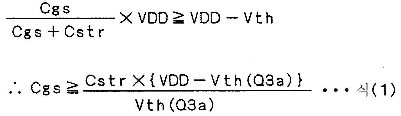
본 실시예의 단위 시프트 레지스터 SR에서는, 용량성분 Cgs는 입력 단자 IN1과 노드 N3 사이의 기생 용량으로, 그 대부분은 트랜지스터 Q3a, Q3b의 게이트·소스 오버랩 용량이다. 따라서 도 10에 나타내는 바와 같이 트랜지스터 Q3a, Q3b 각각의 게이트·소스 오버랩 용량을 Cgso(Q3a), Cgso(Q3b)로 하면, Cgs≒Cgso(Q3a)+Cgso(Q3b)로 할 수 있고, 상기의 식(1)은 다음 식(2)와 같이 변형할 수 있다.In the unit shift register SR of this embodiment, the capacitance component Cgs is a parasitic capacitance between the input terminal IN1 and the node N3, most of which are the gate-source overlap capacitances of the transistors Q3a and Q3b. Therefore, as shown in Fig. 10, when the gate and source overlap capacitances of the transistors Q3a and Q3b are set to Cgso (Q3a) and Cgso (Q3b), it can be set to Cgs ≒ Cgso (Q3a) + Cgso (Q3b). (1) can be modified as in the following formula (2).
[수 2][Number 2]

또한, 트랜지스터 Q3a, Q3b 각각의 게이트·소스 오버랩 용량이 서로 같다고 가정하고, 그 값을 Cgso라고 하면, Cgs≒2×Cgso이므로, 상기의 식(1)은 다음 식(3)과 같이 변형할 수 있다.Further, assuming that the gate-source overlap capacitances of the transistors Q3a and Q3b are equal to each other, and that the value is Cgso, Cgs ≒ 2 × Cgso, so that Equation (1) can be modified as shown in Equation (3) below. have.
[수 3][Number 3]
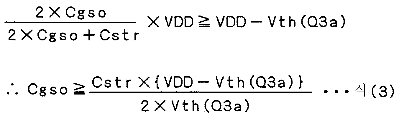
또한 본 실시예에 있어서는, 노드 N1과 제2전원단자 S2 사이에, 게이트가 제1입력 단자 IN1에 접속한 트랜지스터를 2개 직렬접속시킨 구성을 나타냈지만, 3개 이상의 트랜지스터를 직렬접속시켜도 좋다. 그 경우, 그것들의 트랜지스터간의 각 접속 노드에 있어서 식(1)의 조건이 만족되면, 비선택 기간에 각 접속 노드는 VSS이하가 되어, 각 트랜지스터의 임계값 전압의 음의 방향 시프트를 방지할 수 있다.In the present embodiment, a configuration in which two transistors whose gates are connected to the first input terminal IN1 in series is shown between the node N1 and the second power supply terminal S2, but three or more transistors may be connected in series. In that case, if the condition of formula (1) is satisfied in each connection node between these transistors, each connection node becomes VSS or less in the non-selection period, so that the negative direction shift of the threshold voltage of each transistor can be prevented. have.
또 본 실시예에서는, 본 발명에 따른 듀얼 게이트 트랜지스터를 시프트 레지스터 회로에 적용한 예를 도시했지만, 소스 및 드레인의 양쪽에 대하여 게이트를 음으로 바이어스하도록 동작하는 트랜지스터에 널리 적용할 수 있다. 또 본 발명은 a-Si트랜지스터 뿐만아니라, 유기 트랜지스터 등, 임계값 전압의 음의 방향 시프트의 문제를 가지는 각종 트랜지스터에 대해서도 적용가능하다.In the present embodiment, the example in which the dual gate transistor according to the present invention is applied to the shift register circuit is shown, but it can be widely applied to a transistor that operates to negatively bias the gate for both the source and the drain. The present invention is applicable not only to a-Si transistors, but also to various transistors such as organic transistors and the like that have a problem of negative direction shift of the threshold voltage.
<실시예 2><Example 2>
이하의 실시예에 있어서는, 본 발명에 따른 듀얼 게이트 트랜지스터를 적용가능한 시프트 레지스터 회로의 구체적인 예를 나타낸다.In the following embodiments, specific examples of the shift register circuit to which the dual gate transistor according to the present invention can be applied are shown.
도 11은, 실시예 2에 따른 단위 시프트 레지스터 SR의 회로도다. 이 단위 시프트 레지스터 SR은, 도 7의 회로에 대하여, 노드 N1(트랜지스터 Q1의 게이트)을 입력단으로 하고, 노드 N2(트랜지스터 Q2의 게이트)를 출력단으로 하는 인버터를 설치한 것이다. 즉 도 7과 달리, 트랜지스터 Q2의 게이트(노드 N2)는 리셋트 단자 RST에 접속하지 않는다.11 is a circuit diagram of a unit shift register SR according to the second embodiment. This unit shift register SR is provided with the inverter which has node N1 (gate of transistor Q1) as an input terminal, and node N2 (gate of transistor Q2) as an output terminal with respect to the circuit of FIG. That is, unlike FIG. 7, the gate (node N2) of the transistor Q2 is not connected to the reset terminal RST.
이 인버터는, 노드 N2와 제2전원단자 S2 사이에 다이오드 접속한 트랜지스터 Q5와, 노드 N2와 제1전원단자 S1 사이에 접속하여 게이트가 노드 N1에 접속한 트랜지스터 Q6으로 이루어지고 있다. 트랜지스터 Q6은, 트랜지스터 Q5보다도 온 저항이 충분히 작게 설정되어 있다.The inverter consists of a transistor Q5 diode-connected between the node N2 and the second power supply terminal S2, and a transistor Q6 connected between the node N2 and the first power supply terminal S1 and the gate connected to the node N1. The transistor Q6 is set to have a sufficiently smaller on resistance than the transistor Q5.
노드 N1이 L레벨일 때는, 트랜지스터 Q6이 오프하므로 노드 N2는 H레벨(VDD-Vth(Q5))이 된다. 반대로 노드 N1이 H레벨일 때는, 트랜지스터 Q5, Q6모두 온 하지만, 노드 N2는 트랜지스터 Q5, Q6의 온 저항의 비에 의해 결정되는 전위(≒0V)의 L레벨이 된다. 즉, 이 인버터는 소위 「레시오형 인버터」이다.When the node N1 is at the L level, the transistor Q6 is turned off, so the node N2 is at the H level (VDD-Vth (Q5)). On the contrary, when the node N1 is at the H level, both the transistors Q5 and Q6 are turned on, but the node N2 is at the L level of the potential? 0V determined by the ratio of the on resistances of the transistors Q5 and Q6. That is, this inverter is what is called a "recipe-type inverter."
도 7의 단위 시프트 레지스터 SRk에 있어서는, 다음단의 출력 신호 Gk +1이 H레벨이 되었을 때(즉 다음단의 선택 기간)에만 노드 N2가 H레벨이 되므로, 트랜지스터 Q2는 그 기간만 온 하여 출력 단자 OUT를 저임피던스의 L레벨로 한다. 그리고 그 이외의 비선택 기간은 트랜지스터 Q2는 오프가 되고, 출력 단자 OUT는 고임피던스(플로팅 상태)의 L레벨이 된다. 따라서, 출력 신호 Gk가 노이즈나 리크 전류의 영향을 받기 쉬워, 동작이 불안정해지기 쉽다.In the unit shift register SR k in Fig. 7, the node N2 becomes H level only when the output signal G k + 1 of the next stage becomes H level (i.e., the selection period of the next stage). Output terminal OUT to the low impedance L level. In the other non-selection period, the transistor Q2 is turned off, and the output terminal OUT is at the L level of high impedance (floating state). Therefore, the output signal G k is susceptible to the influence of noise and leakage current, and the operation tends to be unstable.
그것에 대해 도 11의 단위 시프트 레지스터 SRk에서는, 노드 N1이 L레벨 동안, 트랜지스터 Q5, Q6으로 이루어지는 인버터가 노드 N2를 H레벨로 유지하므로, 비선택 기간 동안, 트랜지스터 Q2는 온 상태로 유지된다. 즉, 비선택 기간에 있어 서의 출력 단자 OUT(출력 신호 G)가 저임피던스로 L레벨로 유지되므로, 동작이 안정된다.On the other hand, in the unit shift register SR k in Fig. 11, while the node N1 is at the L level, the inverter composed of the transistors Q5 and Q6 maintains the node N2 at the H level, so that the transistor Q2 is kept on during the non-selection period. That is, since the output terminal OUT (output signal G) in the non-selection period is kept at the L level with low impedance, the operation is stabilized.
물론 본 실시예에 있어서도, 듀얼 게이트 트랜지스터 Q3D를 구성하는 트랜지스터 Q3a, Q3b의 임계값 전압의 음의 방향 시프트가 억제되는 효과를 얻을 수 있다. 따라서, 비선택 기간에 노드 N1의 레벨이 상승하는 것을 방지할 수 있고, 오동작의 발생을 방지할 수 있다.Of course, also in this embodiment, the negative direction shift of the threshold voltage of the transistors Q3a and Q3b which comprise the dual gate transistor Q3D can be obtained. Therefore, it is possible to prevent the level of the node N1 from rising in the non-selection period, and prevent the occurrence of malfunction.
<실시예 3><Example 3>
도 12는, 실시예 3에 따른 단위 시프트 레지스터 SR의 회로도다. 이 단위 시프트 레지스터 SR은, 도 11의 회로에 대하여, 노드 N1과 제1전원단자 S1 사이에 접속하고, 게이트가 노드 N2에 접속한 트랜지스터 Q7을 설치한 것이다. 즉, 트랜지스터 Q7은, 노드 N2에 접속한 게이트 전극을 가지고, 노드 N1을 방전하는 트랜지스터다.12 is a circuit diagram of a unit shift register SR according to the third embodiment. This unit shift register SR is connected between the node N1 and the first power supply terminal S1 in the circuit of FIG. 11, and a transistor Q7 having a gate connected to the node N2 is provided. That is, transistor Q7 is a transistor which has the gate electrode connected to node N2, and discharges node N1.
도 11의 단위 시프트 레지스터 SRk에 있어서는, 다음단의 출력 신호 Gk +1이 H레벨이 되었을 때(다음단의 선택 기간)에, 트랜지스터 Q4가 온 하여 노드 N1을 방전하지만, 그 이외의 비선택 기간에 있어서는 노드 N1은 고임피던스(플로팅 상태)로 L레벨이 된다. 따라서, 비선택 기간에 노이즈나 리크 전류에 의해 노드 N1로 전하가 공급되면, 노드 N1의 레벨이 상승한다. 그렇게 되면 트랜지스터 Q1이 온 하여, 오신호로서 출력 신호 G가 출력되는 오동작이 생긴다.In the unit shift register SR k in FIG. 11, when the output signal G k +1 of the next stage becomes H level (selection period of the next stage), the transistor Q4 is turned on and the node N1 is discharged. In the selection period, the node N1 becomes L level with high impedance (floating state). Therefore, when charge is supplied to the node N1 by noise or leakage current in the non-selection period, the level of the node N1 increases. In this case, the transistor Q1 is turned on, resulting in a malfunction in which the output signal G is output as an error signal.
그것에 대해 도 12의 단위 시프트 레지스터 SR에 있어서는, 노드 N1이 L레벨 이 되면, 트랜지스터 Q5, Q6으로 이루어지는 인버터가 노드 N2를 H레벨로 하고, 따라서 트랜지스터 Q7이 온이 되므로, 노드 N1은 비선택 기간 동안 저임피던스로 L레벨이 된다. 따라서, 비선택 기간에 노드 N1의 레벨이 상승하는 것이 억제되어, 상기의 오동작의 발생이 방지된다.On the other hand, in the unit shift register SR of Fig. 12, when the node N1 becomes L level, the inverter composed of transistors Q5 and Q6 sets the node N2 to H level, and thus the transistor Q7 is turned on, so that the node N1 is in the non-selection period. L level at low impedance. Therefore, the increase of the level of the node N1 in the non-selection period is suppressed, and the occurrence of the above malfunction is prevented.
또한, 트랜지스터 Q7은, 듀얼 게이트 트랜지스터 Q3D가 노드 N1의 레벨을 상승시키는 것이 가능하도록, 듀얼 게이트 트랜지스터 Q3D보다도 온 저항이 충분 큰 것이다.In addition, the transistor Q7 is sufficiently large on-resistance than the dual gate transistor Q3D so that the dual gate transistor Q3D can raise the level of the node N1.
본 실시예에 있어서도, 듀얼 게이트 트랜지스터 Q3D를 구성하는 트랜지스터 Q3a, Q3b의 임계값 전압의 음의 방향 시프트가 억제되는 효과를 얻을 수 있다. 본 실시예에서는, 가령 비선택 기간에 듀얼 게이트 트랜지스터 Q3D에 전류가 흘러서 노드 N1에 전하가 공급된다고 해도, 그 전하는 트랜지스터 Q7에 의해 제1전원단자 S1에 방출되므로, 그것에 의한 오동작은 잘 일어나지 않는다. 그러나 그 전류는, 단위 시프트 레지스터 SR의 소비 전력의 증대나, 고전위측 전원전위 VDD의 저하를 초래한다. 따라서, 듀얼 게이트 트랜지스터 Q3D의 임계값 전압의 음의 방향 시프트를 방지하는 것은, 본 실시예에 있어서도 매우 유효하다.Also in this embodiment, the effect that the negative direction shift of the threshold voltages of the transistors Q3a and Q3b constituting the dual gate transistor Q3D is suppressed can be obtained. In the present embodiment, even if a current flows through the dual gate transistor Q3D during the non-selection period, and electric charge is supplied to the node N1, the charge is discharged to the first power supply terminal S1 by the transistor Q7, so that malfunction is not easily caused. However, the current causes an increase in power consumption of the unit shift register SR and a drop in the high potential power supply potential VDD. Therefore, preventing the negative direction shift of the threshold voltage of the dual gate transistor Q3D is very effective also in this embodiment.
<실시예 4><Example 4>
실시예 2, 3에서 설명한 바와 같이, 도 11 및 도 12의 단위 시프트 레지스터 SR에 있어서는, 비선택 기간 동안 트랜지스터 Q2의 게이트(노드 N2)가 계속해서 H레벨이 되는 것으로, 출력 단자 OUT를 저임피던스의 L레벨로 할 수 있다. 그러나, a-Si트랜지스터의 게이트가 소스에 대하여 계속적으로 양 바이어스되면, 임계값 전 압이 양 방향으로 시프트한다. 트랜지스터 Q2에서 임계값 전압의 양방향 시프트가 일어나면, 이 트랜지스터 Q2의 온 저항이 높아지고, 출력 단자 OUT를 충분히 저임피던스로 할 수 없게 되는 문제가 생긴다.As described in
또 도 12의 단위 시프트 레지스터 SR에 있어서는, 트랜지스터 Q7의 게이트도, 비선택 기간 동안, 계속해서 H레벨이 되므로, 이 트랜지스터 Q7의 임계값 전압도 양방향으로 시프트하고, 노드 N1을 출력 단자 OUT를 충분히 저임피던스로 할 수 없게 되는 문제도 생긴다.In the unit shift register SR of Fig. 12, the gate of the transistor Q7 also becomes H level during the non-selection period, so that the threshold voltage of the transistor Q7 is also shifted in both directions, and the node N1 is provided with sufficient output terminal OUT. There is also a problem that cannot be done with low impedance.
도 13은, 실시예 4에 따른 단위 시프트 레지스터 SR의 회로도이며, 그 문제의 대책이 실시된 것이다. 도 13의 단위 시프트 레지스터 SR은, 출력 단자 OUT를 방전하는 트랜지스터(도 11 및 도 12의 트랜지스터 Q2에 해당한다)가 병렬로 2개 설치되어 있다(트랜지스터 Q2A, Q2B). 여기에서, 트랜지스터 Q2A, Q2B의 게이트가 접속하는 노드를 각각 「노드 N2A」, 「노드 N2B」라고 정의한다.Fig. 13 is a circuit diagram of the unit shift register SR according to the fourth embodiment, in which countermeasures for the problem are implemented. In the unit shift register SR of FIG. 13, two transistors (corresponding to transistors Q2 of FIGS. 11 and 12) for discharging the output terminal OUT are provided in parallel (transistors Q2A and Q2B). Here, the nodes to which the gates of the transistors Q2A and Q2B are connected are defined as "node N2A" and "node N2B", respectively.
또 이 단위 시프트 레지스터 SR에는, 도 12의 트랜지스터 Q7에 해당하는 것이, 노드 N2A, N2B의 각각에 설치된다(트랜지스터 Q7A, Q7B). 즉 트랜지스터 Q7A는, 노드 N2A에 접속한 게이트 전극을 가지고 노드 N1을 방전하는 트랜지스터이며, 트랜지스터 Q7B는, 노드 N2B에 접속한 게이트 전극을 가지고 노드 N1을 방전하는 트랜지스터다.Incidentally, the unit shift register SR corresponds to the transistor Q7 shown in FIG. 12 at each of the nodes N2A and N2B (transistors Q7A and Q7B). That is, transistor Q7A is a transistor which discharges node N1 with the gate electrode connected to node N2A, and transistor Q7B is a transistor which discharges node N1 with the gate electrode connected to node N2B.
본 실시예에 따른 단위 시프트 레지스터 SR은, 소정의 제어신호 VFRA가 입력되는 제1제어 단자 TA 및 제어신호 VFRB가 입력되는 제2제어 단자 TB를 가지고 있다. 제어신호 VFRA, VFRB는 서로 상보인 신호이며, 시프트 레지스터 외부의 제어장 치(도시하지 않음)에 의해 생성된다. 이 제어신호 VFRA, VFRB는, 일정한 주기로 레벨이 바뀌는 것이다. 게이트선 구동회로에서는, 표시 화상의 프레임 간의 블랭킹 기간에 레벨이 바뀌도록(교대하도록) 제어되는 것이 바람직하고, 예를 들면 표시 화상의 1프레임 마다 레벨이 바뀌도록 제어된다.The unit shift register SR according to the present embodiment has a first control terminal TA to which a predetermined control signal VFRA is input and a second control terminal TB to which a control signal VFRB is input. The control signals VFRA and VFRB are complementary signals, and are generated by a control device (not shown) outside the shift register. The control signals VFRA and VFRB change their levels at regular intervals. In the gate line driver circuit, it is preferable that the level is controlled so as to change (alternatively) in the blanking period between the frames of the display image, and for example, the level is controlled to change every frame of the display image.
또 제1제어 단자 TA와 노드 N2A 사이에는 트랜지스터 Q8A가 접속하고, 제2제어 단자 TB와 노드 N2B 사이에는 트랜지스터 Q8B가 접속한다. 트랜지스터 Q8A의 게이트는 노드 N2B에 접속하고, 트랜지스터 Q8B의 게이트는 노드 2A에 접속한다. 즉, 트랜지스터 Q8A 및 트랜지스터 Q8B는, 그 한쪽의 주 전극(여기에서는 드레인)이 서로 교차하도록 제어 전극(게이트)에 접속되어, 소위 플립플롭회로를 구성하고 있다.The transistor Q8A is connected between the first control terminal TA and the node N2A, and the transistor Q8B is connected between the second control terminal TB and the node N2B. The gate of the transistor Q8A is connected to the node N2B, and the gate of the transistor Q8B is connected to the node 2A. That is, the transistors Q8A and Q8B are connected to the control electrode (gate) so that one main electrode (here, the drain) intersects each other, and constitutes a so-called flip-flop circuit.
또한 이 단위 시프트 레지스터 SR은, 트랜지스터 Q5, Q6으로 이루어지는 인버터의 출력단과 노드 N2A 사이에 접속하는 트랜지스터 Q9A와, 이 인버터의 출력단과 노드 N2B 사이에 접속하는 트랜지스터 Q9B를 구비하고 있다. 트랜지스터 Q9A의 게이트는 제1제어 단자 TA에 접속하고, 트랜지스터 Q9B의 게이트는 제2제어 단자 TB에 접속한다.The unit shift register SR further includes a transistor Q9A connected between the output terminal of the inverter consisting of transistors Q5 and Q6 and the node N2A, and a transistor Q9B connected between the output terminal of the inverter and the node N2B. The gate of the transistor Q9A is connected to the first control terminal TA, and the gate of the transistor Q9B is connected to the second control terminal TB.
제어신호 VFRA가 H레벨, 제어신호 VFRB이 L레벨의 기간은, 트랜지스터 Q9A가 온, 트랜지스터 Q9B가 오프가 되므로, 트랜지스터 Q5, Q6으로 이루어지는 인버터의 출력단은 노드 N2A에 접속된다. 또 이 때 트랜지스터 Q8B가 온 하고, 노드 N2A는 L레벨이 된다. 즉 그 기간에는, 트랜지스터 Q2A가 구동되고, 트랜지스터 Q2B는 비활성 상태가 된다.In the period where the control signal VFRA is at the H level and the control signal VFRB is at the L level, the transistor Q9A is turned on and the transistor Q9B is turned off. Therefore, the output terminal of the inverter consisting of the transistors Q5 and Q6 is connected to the node N2A. At this time, transistor Q8B is turned on and node N2A is at L level. That is, in that period, the transistor Q2A is driven and the transistor Q2B is inactive.
반대로, 제어신호 VFRA가 L레벨, 제어신호 VFRB가 H레벨의 기간은, 트랜지스터 Q9A가 오프, 트랜지스터 Q9B가 온이 되므로, 트랜지스터 Q5, Q6으로 이루어지는 인버터의 출력단은 노드 N2B에 접속된다. 또 이 때 트랜지스터 Q8A가 온 하고, 노드 N2B는 L레벨이 된다. 즉 그 기간에는, 트랜지스터 Q2B가 구동되고, 트랜지스터 Q2A는 비활성 상태가 된다.On the contrary, since the transistor Q9A is turned off and the transistor Q9B is turned on during the period in which the control signal VFRA is at the L level and the control signal VFRB is at the H level, the output terminal of the inverter consisting of the transistors Q5 and Q6 is connected to the node N2B. At this time, transistor Q8A is turned on and node N2B is at L level. That is, in that period, the transistor Q2B is driven and the transistor Q2A is inactive.
이와 같이, 트랜지스터 Q9A, Q9B는, 제어신호 VFRA, VFRB에 의거하여 트랜지스터 Q5, Q6으로 이루어지는 인버터의 출력단을, 노드 N2A 및 노드 N2B에 교대로 접속시키는 변환회로로서 기능한다.Thus, the transistors Q9A and Q9B function as a conversion circuit for alternately connecting the output terminals of the inverters consisting of the transistors Q5 and Q6 to the node N2A and the node N2B based on the control signals VFRA and VFRB.
본 실시예에 있어서는, 제어신호 VFRA, VFRB가 반전할 때마다, 트랜지스터 Q2A, Q5A의 페어와 트랜지스터 Q2B, Q5B의 페어가 교대로 비활성 상태가 되는 것으로, 그것들의 게이트가 계속적으로 바이어스되는 것을 방지할 수 있다. 따라서, a-Si트랜지스터의 임계값의 양방향 시프트에 의한 오동작을 방지할 수 있고, 동작의 신뢰성이 향상된다.In this embodiment, whenever the control signals VFRA and VFRB are inverted, the pairs of transistors Q2A and Q5A and the pairs of transistors Q2B and Q5B are alternately inactive, thereby preventing their gates from being continuously biased. Can be. Therefore, the malfunction due to the bi-directional shift of the threshold value of the a-Si transistor can be prevented, and the reliability of the operation is improved.
본 실시예에 있어서도, 듀얼 게이트 트랜지스터 Q3D를 구성하는 트랜지스터 Q3a, Q3b의 임계값 전압의 음의 방향 시프트가 억제되는 효과를 얻을 수 있다. 그것에 의해, 단위 시프트 레지스터 SR의 오동작의 발생, 소비 전력의 증대 및 전원전압의 저하를 방지할 수 있다.Also in this embodiment, the effect that the negative direction shift of the threshold voltages of the transistors Q3a and Q3b constituting the dual gate transistor Q3D is suppressed can be obtained. This can prevent the occurrence of malfunction of the unit shift register SR, an increase in power consumption, and a decrease in power supply voltage.
<실시예 5><Example 5>
상기의 각 실시예에 있어서, 듀얼 게이트 트랜지스터 Q3D는, 단위 시프트 레지스터 SR의 노드 N1의 충전시, 소스폴로어 모드에서 동작한다. 즉, 노드 N1의 충 전이 진행됨에 따라, 트랜지스터 Q3b의 게이트(입력 단자 IN1)·소스(노드 N1)간 전압이 작아져 구동능력(전류를 흐르게 하는 능력)이 저하하므로, 노드 N1을 충분히 높은 레벨까지 충전하기 위해 어느 정도의 시간을 필요로 한다. 이것은 시프트 레지스터 동작의 고속화에 있어 방해가 된다.In each of the above embodiments, the dual gate transistor Q3D operates in the source follower mode when the node N1 of the unit shift register SR is charged. In other words, as charging of the node N1 proceeds, the voltage between the gate (input terminal IN1) and the source (node N1) of the transistor Q3b decreases and the driving ability (the ability to flow current) decreases, so that the node N1 is sufficiently high. It needs some time to charge up. This hinders the speed of the shift register operation.
도 14는, 실시예 5에 따른 단위 시프트 레지스터 SR의 회로도로서, 그 문제의 대책이 실시된 것이다. 이 단위 시프트 레지스터 SR은, 종속 접속할 경우에는 도 15에 나타내는 바와 같이 서로 위상이 다른 3상 클록 CLKA, CLKB, CLKC를 사용하여 구동된다.Fig. 14 is a circuit diagram of the unit shift register SR according to the fifth embodiment, in which countermeasures for the problem are implemented. In the case of cascading, this unit shift register SR is driven using three-phase clocks CLKA, CLKB, and CLKC, which are different in phase from each other, as shown in FIG.
또한 각 단위 시프트 레지스터 SR은, 입력 단자로서 제1입력 단자 IN1 및 제2입력 단자 IN2의 2개를 가지고 있으며, 제1입력 단자 IN1에는 앞앞단(2단 앞)의 출력 단자 OUT에 접속되고, 제2입력 단자 IN2에는 앞단(1단 앞)의 출력 단자 OUT에 접속된다. 또한 제1단째의 단위 시프트 레지스터 SR1의 제1입력 단자 IN1, 제2입력 단자 IN2에는, 각각 스타트 펄스 ST1, ST2가 입력된다. 스타트 펄스 ST1, ST2는 활성화하는(H레벨이 되는) 타이밍이 다르고, 스타트 펄스 ST2는 스타트 펄스 ST1 뒤에 활성화한다.In addition, each unit shift register SR has two as an input terminal, a 1st input terminal IN1 and a 2nd input terminal IN2, and is connected to the output terminal OUT of the front front end (the front 2nd stage) to the 1st input terminal IN1, The second input terminal IN2 is connected to the output terminal OUT at the front end (first stage). Further, start pulses ST1 and ST2 are input to the first input terminal IN1 and the second input terminal IN2 of the unit shift register SR1 of the first stage, respectively. The start pulses ST1 and ST2 have different timings of activation (to become H level), and the start pulse ST2 is activated after the start pulse ST1.
본 실시예의 단위 시프트 레지스터 SR은, 노드 N1을 충전하는 수단으로서, 듀얼 게이트 트랜지스터 Q3D와, 그 게이트 노드(「노드 N4」라고 정의한다)를 충전하는 트랜지스터 Q1O과, 노드 N4를 승압하는 용량소자 C2와, 노드 N4를 방전하는 트랜지스터 Q4를 포함하고 있다. 도 14에 나타내는 바와 같이 트랜지스터 Q1O은, 노드 N4와 제2전원단자 S2 사이에 접속하고, 게이트가 제1입력 단자 IN1에 접속한 다. 용량소자 C2는 노드 N4와 제2입력 단자 IN2 사이에 접속한다. 트랜지스터 Q4는, 노드 N4와 제1전원단자 S1 사이에 접속하고, 게이트가 리셋트 단자 RST에 접속되어 있다.The unit shift register SR of the present embodiment is a means for charging the node N1, the dual gate transistor Q3D, the transistor Q10 for charging the gate node (defined as "node N4"), and the capacitor C2 for boosting the node N4. And a transistor Q4 for discharging the node N4. As shown in Fig. 14, the transistor Q10 is connected between the node N4 and the second power supply terminal S2, and the gate is connected to the first input terminal IN1. The capacitor C2 is connected between the node N4 and the second input terminal IN2. The transistor Q4 is connected between the node N4 and the first power supply terminal S1, and the gate is connected to the reset terminal RST.
이 단위 시프트 레지스터 SR은, 노드 N4를 입력단으로 하는 인버터(트랜지스터 Q5, Q6)를 구비하고, 출력 단자 OUT 및 노드 N1을 각각 방전하는 트랜지스터 Q2, Q7의 게이트(노드 N2)는 모두, 이 인버터의 출력단에 접속된다. 또 노드 N4와 제1전원단자 S1 사이에는, 트랜지스터 Q4와 병렬로 트랜지스터 Q11이 접속되고, 그 게이트는 노드 N2에 접속되어 있다.The unit shift register SR includes an inverter (transistors Q5 and Q6) having the node N4 as an input terminal, and all of the gates (node N2) of the transistors Q2 and Q7 which discharge the output terminal OUT and the node N1, respectively, It is connected to the output terminal. In addition, the transistor Q11 is connected in parallel with the transistor Q4 between the node N4 and the first power supply terminal S1, and the gate thereof is connected to the node N2.
도 14의 단위 시프트 레지스터 SR의 기본적인 동작 이론은, 실시예 1에서 설명한 것과 거의 동일하지만, 노드 N1을 충전하는 듀얼 게이트 트랜지스터 Q3D의 게이트가, 앞단 및 앞앞단 각각의 출력 신호와 같은 2개의 신호를 사용하여 충전·승압되는 점에 특징이 있다.The basic operation theory of the unit shift register SR of FIG. 14 is almost the same as that described in
즉 단위 시프트 레지스터 SRk에 있어서, 듀얼 게이트 트랜지스터 Q3D의 게이트(노드 N4)는, 우선 앞앞단의 출력 신호 Gk -2가 H레벨이 될 때, 트랜지스터 Q1O에 의해 VDD-Vth(Q10)의 레벨까지 프리챠지된다. 이어서 앞단의 출력 신호 Gk -1이 H레벨이 될 때에는, 노드 N4는 용량소자 C2에 의해 2×VDD-Vth(10)정도까지 승압된다. 즉 듀얼 게이트 트랜지스터 Q3D의 게이트 전위는, 도 1의 회로의 경우보다도 VDD정도 높아지고, 이 듀얼 게이트 트랜지스터 Q3D는, 소스폴로어 모드가 아닌 비포화 영역에서의 동작에 의해 노드 N1을 충전할 수 있다. 따라서, 노드 N1은 고속으로 충전되어 H레벨(VDD)이 되므로, 상기의 문제가 해결된다.I.e. in the unit of the shift register SR k, the gate of the dual gate transistor Q3D (node N4), first, when the output signal G k -2 front of the front end is at the H level, the level of VDD-Vth (Q10) by the transistor Q1O Precharged to Subsequently, when the preceding output signal G k -1 becomes H level, the node N4 is boosted to about 2 x VDD-Vth (10) by the capacitor C2. That is, the gate potential of the dual gate transistor Q3D is about VDD higher than in the case of the circuit of FIG. 1, and the dual gate transistor Q3D can charge the node N1 by operation in an unsaturated region other than the source follower mode. Therefore, since the node N1 is charged at high speed and becomes H level (VDD), the above problem is solved.
또한 본 실시예에서는, 선택 기간에 있어서 듀얼 게이트 트랜지스터 Q3D의 게이트(노드 N4)는 플로팅 상태가 되므로, 다음단의 출력 신호 Gk +1에 의해 제어되는 트랜지스터 Q4는, 이 노드 N4의 방전에 이용되고 있다(이 점에서, 도 7의 트랜지스터 Q4와는 다르다). 트랜지스터 Q4가 노드 N4를 L레벨로 하면, 트랜지스터 Q5, Q6으로 이루어지는 인버터에 의해 노드 N2가 H레벨이 되고, 따라서 트랜지스터 Q7이 온 하여 노드 N1을 방전한다. 즉 본 실시예에서는, 리셋트 단자 RST에 입력되는 신호에 따라 노드 N1을 방전하는 역할(즉, 도 7에 있어서의 트랜지스터 Q4의 역할)은, 트랜지스터 Q7이 담당하고 있다.In the present embodiment, since the gate (node N4) of the dual gate transistor Q3D is in the floating state in the selection period, the transistor Q4 controlled by the output signal G k +1 of the next stage is used for discharge of this node N4. (In this respect, it is different from transistor Q4 of FIG. 7). When transistor Q4 sets node N4 to L level, node N2 becomes H level by the inverter which consists of transistors Q5 and Q6. Therefore, transistor Q7 turns on and discharges node N1. In other words, in the present embodiment, the transistor Q7 is responsible for discharging the node N1 in response to the signal input to the reset terminal RST (that is, the role of the transistor Q4 in FIG. 7).
또한 트랜지스터 Q11은, 노드 N2가 H레벨이 되는 동안(비선택 기간), 노드 N4를 저임피던스의 L레벨로 유지하도록 동작하고, 그것에 의해 이 단위 시프트 레지스터 SR의 오동작이 방지되고 있다.In addition, the transistor Q11 operates to maintain the node N4 at the low impedance L level while the node N2 is at the H level (non-selection period), thereby preventing the malfunction of the unit shift register SR.
본 실시예에 있어서도, 듀얼 게이트 트랜지스터 Q3D를 구성하는 트랜지스터 Q3a, Q3b의 임계값 전압의 음의 방향 시프트가 억제되는 효과를 얻을 수 있다. 그것에 의해, 단위 시프트 레지스터 SR의 오동작의 발생, 소비 전력의 증대 및 전원전압의 저하를 방지할 수 있다.Also in this embodiment, the effect that the negative direction shift of the threshold voltages of the transistors Q3a and Q3b constituting the dual gate transistor Q3D is suppressed can be obtained. This can prevent the occurrence of malfunction of the unit shift register SR, an increase in power consumption, and a decrease in power supply voltage.
또 도 14의 단위 시프트 레지스터 SR에서는, 트랜지스터 Q1O이 노드 N4를 충전한 후에, 앞앞단의 출력 신호 Gk -2가 L레벨이 되었을 때, 트랜지스터 Q1O의 게이트가 소스 및 드레인보다도 낮은 전위가 된다. 그 때문에 트랜지스터 Q10에 있어서 도 도 1의 트랜지스터 Q3과 동일한 임계값 전압의 음의 방향 시프트의 문제가 생길 가능성이 있다.In the unit shift register SR of FIG. 14, after the transistor Q1O charges the node N4, when the output signal G k -2 of the preceding front becomes L level, the gate of the transistor Q10 becomes lower than the source and the drain. Therefore, there exists a possibility that the problem of the negative direction shift of the threshold voltage similar to transistor Q3 of FIG. 1 may arise in transistor Q10.
그래서 그 문제를 회피하기 위해, 도 14의 트랜지스터 Q1O에 대해서도 본 발명의 듀얼 게이트 트랜지스터를 적용해도 된다. 즉 이 트랜지스터 Q10을, 도 16에 나타내는 바와 같이 트랜지스터 Q1Oa, Q1Ob로 이루어지는 듀얼 게이트 트랜지스터 Q1OD로 치환해도 된다. 이 듀얼 게이트 트랜지스터 Q1OD도, 상기의 듀얼 게이트 트랜지스터 Q3D와 마찬가지로, 그 게이트 전극이 H레벨에서 L레벨로 변화되었을 때, 그것에 따라 트랜지스터 Q1Oa, Q1Ob 사이의 접속 노드(「노드 N1O」이라고 정의)가 L레벨로 낮아지도록, 이 게이트와 노드 N6 사이의 기생 용량을 크게 한 것이다.Therefore, in order to avoid the problem, the dual gate transistor of the present invention may also be applied to the transistor Q10 of FIG. That is, this transistor Q10 may be replaced with the dual gate transistor Q1OD which consists of transistors Q10a and Q10b, as shown in FIG. Similarly to the above-mentioned dual gate transistor Q3D, this dual gate transistor Q1OD also has a connection node (defined as "node N1O") between transistors Q1Oa and Q10O when its gate electrode changes from H level to L level. The parasitic capacitance between the gate and node N6 is increased to lower to the level.
이 구성에 의하면, 듀얼 게이트 트랜지스터 Q10D 즉 트랜지스터 Q1Oa, Q10b에 있어서, 임계값 전압의 음의 방향 시프트를 억제하는 효과를 얻을 수 있고, 본 실시예에 따른 단위 시프트 레지스터 SR의 오동작의 발생, 소비 전력의 증대 및 전원전압의 저하를 방지할 수 있다.According to this configuration, in the dual gate transistor Q10D, i.e., the transistors Q10a and Q10b, the effect of suppressing the negative direction shift of the threshold voltage can be obtained, and the malfunction and power consumption of the unit shift register SR according to the present embodiment can be obtained. Can be prevented from increasing and the power supply voltage from falling.
<실시예 6><Example 6>
실시예 4에 있어서는, 비선택 기간에 출력 단자 OUT 및 노드 N1을 각각 저임피던스의 L레벨로 하기 위한 트랜지스터 Q2, Q7에 있어서의 임계값 전압의 양방향 시프트의 문제를 해결하는 방법의 하나를 설명했다. 본 실시예에 있어서도, 그 문제를 해결하는 방법을 나타낸다.In Example 4, one method of solving the problem of the bidirectional shift of the threshold voltages in the transistors Q2 and Q7 for setting the output terminal OUT and the node N1 to the low impedance L level in the non-selection period, respectively, has been described. Also in this embodiment, the method of solving the problem is shown.
도 17은, 실시예 6에 따른 단위 시프트 레지스터 SR의 회로도다. 이 단위 시프트 레지스터 SR은, 클록 단자를 2개를 가지고 있다. 즉, 트랜지스터 Q1의 드레인 이 접속하는 제1클록 단자 CK1에 더하여, 그것에 입력되는 것과는 다른 위상의 클록 신호가 입력되는 제2클록 단자 CK2를 구비하고 있다.17 is a circuit diagram of a unit shift register SR according to the sixth embodiment. This unit shift register SR has two clock terminals. That is, in addition to the first clock terminal CK1 to which the drain of the transistor Q1 is connected, the second clock terminal CK2 to which a clock signal having a phase different from that input thereto is input.
또 노드 N1과 출력 단자 OUT 사이에, 게이트가 제1클록 단자 CK1에 접속한 트랜지스터 Q12가 설치되는 동시에, 트랜지스터 Q5, Q6으로 이루어지는 인버터의 출력단(「노드 N5」라고 정의한다)과 제1전원단자 S1 사이에, 게이트가 제1클록 단자 CK1에 접속한 트랜지스터 Q13이 설치된다. 또한 본 실시예에서는, 출력 단자 OUT와 제1전원단자 S1 사이에 접속한 트랜지스터 Q2의 게이트는, 제2클록 단자 CK2에 접속된다.In addition, between the node N1 and the output terminal OUT, a transistor Q12 having a gate connected to the first clock terminal CK1 is provided, and an output terminal (defined as "node N5") and a first power supply terminal of the inverter consisting of transistors Q5 and Q6. Between S1, the transistor Q13 with the gate connected to the 1st clock terminal CK1 is provided. In this embodiment, the gate of the transistor Q2 connected between the output terminal OUT and the first power supply terminal S1 is connected to the second clock terminal CK2.
트랜지스터 Q5, Q6으로 이루어지는 인버터는, 실시예 2, 3과 마찬가지로 노드 N1을 입력단으로 하고 있지만, 트랜지스터 Q5의 게이트 및 드레인이 제2클록 단자 CK2에 접속되는 점에서 다르다. 즉 제2클록 단자 CK2에 입력되는 클록 신호는, 이 인버터의 전원이 된다.Inverters composed of transistors Q5 and Q6 have nodes N1 as input terminals in the same manner as in
도 17의 단위 시프트 레지스터 SR의 기본적인 동작 이론은, 실시예 1에서 설명한 것과 거의 동일하지만, 트랜지스터 Q5, Q6으로 이루어지는 인버터가, 제2클록 단자 CK2에 입력되는 클록 신호에 의해 전력이 공급되는 것으로 활성화되고, 또한 그 출력은 트랜지스터 Q13에 의해 강제적으로 L레벨 되는 점이 특징적이다.The basic operation theory of the unit shift register SR of FIG. 17 is almost the same as that described in
여기에서도 제k단째의 단위 시프트 레지스터 SRk의 동작을 대표적으로 설명한다. 간단히 하기 위해, 이 단위 시프트 레지스터 SRk에 있어서는, 제1클록 단자 CK1에 클록 신호 CLKA가 입력되고, 제2클록 단자 CK2에 클록 신호 CLKB가 입력되는 것으로 한다.Here, the operation of the k-th unit shift register SR k is representatively described. For simplicity, it is assumed that the clock signal CLKA is input to the first clock terminal CK1 and the clock signal CLKB is input to the second clock terminal CK2 in this unit shift register SR k .
우선, 단위 시프트 레지스터 SRk의 비선택 기간의 동작에 대해 설명한다. 비선택 기간에서는, 노드 N1은 L레벨이므로, 트랜지스터 Q5, Q6으로 이루어지는 인버터가 클록 신호 CLKB에 의해 활성화되면 노드 N5가 H레벨이 된다. 또 이 인버터가 비활성이 될 때는, 트랜지스터 Q13이 클록 신호 CLKA에 의해 온이 되므로, 노드 N5는 L레벨이 된다. 즉, 비선택 기간에 있어서는, 노드 N5는 거의 클록 신호 CLKB와 같이 레벨이 변화하게 된다. 따라서 트랜지스터 Q7은, 클록 신호 CLKB가 H레벨이 되는 타이밍에서 노드 N1을 저임피던스의 L레벨로 한다.First, the operation of the non-selection period of the unit shift register SR k will be described. In the non-selection period, since the node N1 is at the L level, the node N5 is at the H level when the inverter composed of the transistors Q5 and Q6 is activated by the clock signal CLKB. When the inverter is inactive, the transistor Q13 is turned on by the clock signal CLKA, so that the node N5 is at the L level. In other words, in the non-selection period, the node N5 almost changes in level like the clock signal CLKB. Therefore, transistor Q7 sets node N1 to L level of low impedance at the timing when clock signal CLKB becomes H level.
트랜지스터 Q7은, 클록 신호 CLKB가 L레벨일 때에는 오프가 되지만, 그 동안은 클록 신호 CLKA가 트랜지스터 Q12를 온으로 하므로, 노드 N1의 전하는 트랜지스터 Q12에 의해 출력 단자 OUT에 방출된다. 통상, 출력 단자 OUT에는 용량성의 부하(게이트선 구동회로의 경우에는, 표시 패널의 게이트선)가 접속되므로, 이 때 출력 단자 OUT에 방출될 정도의 전하로는, 출력 단자 OUT가 H레벨이 되지 않는다.The transistor Q7 is turned off when the clock signal CLKB is at L level. However, since the clock signal CLKA turns on the transistor Q12, the charge of the node N1 is discharged to the output terminal OUT by the transistor Q12. In general, since a capacitive load (gate line of the display panel in the case of a gate line driver circuit) is connected to the output terminal OUT, the output terminal OUT does not become H level with a charge that is discharged to the output terminal OUT at this time. Do not.
이와 같이 단위 시프트 레지스터 SRk의 비선택 기간에 있어서는, 트랜지스터 Q7과 트랜지스터 Q12가 교대로 노드 N1을 방전하도록 동작함으로써 노드 N1의 레벨 상승이 방지되고 있다. 트랜지스터 Q7, Q12의 게이트 전극은 계속적으로 양 바이어스되지 않으므로, 그것들의 임계값 전압의 양방향 시프트는 억제된다.In this manner, in the non-selection period of the unit shift register SR k , the transistor Q7 and the transistor Q12 operate to discharge the node N1 alternately, thereby preventing the level rise of the node N1. Since the gate electrodes of the transistors Q7 and Q12 are not continuously positively biased, the bidirectional shift of their threshold voltages is suppressed.
또한 트랜지스터 Q2는, 클록 신호 CLKB가 H레벨이 될 때 온 하고, 출력 단자 OUT를 저임피던스의 L레벨로 한다. 즉 트랜지스터 Q2의 게이트도 계속적으로 양 바 이어스 되지 않으므로, 그 임계값 전압의 양방향 시프트도 억제된다.The transistor Q2 is turned on when the clock signal CLKB becomes H level, and the output terminal OUT is set to the low impedance L level. In other words, since the gate of the transistor Q2 is not continuously biased, the bidirectional shift of the threshold voltage is also suppressed.
또한 앞단의 출력 신호 Gk -1이 H레벨이 되고, 단위 시프트 레지스터 SRk의 선택기간이 되면, 노드 N1이 H레벨이 된다. 그 동안은, 트랜지스터 Q5, Q6으로 이루어지는 인버터가 클록 신호 CLKB에 의해 활성화되어도 노드 N5는 L레벨이므로, 트랜지스터 Q7은 오프가 되어 노드 N1의 H레벨은 유지된다. 그리고 클록 신호 CLKA가 H레벨이 되면, 트랜지스터 Q12의 게이트가 H레벨이 되지만, 그것과 동시에 출력 단자 OUT(출력 신호 Gk)도 H레벨이 되므로, 트랜지스터 Q12는 온 하지 않고, 노드 N1은 플로팅 상태에서 H레벨로 유지된다(클록 신호 CLKA에 의해 승압된다). 따라서, 단위 시프트 레지스터 SRk는, 정상적으로 출력 신호 Gk를 출력할 수 있다.In addition, when the output signal G k- 1 of the preceding stage becomes H level and the selection period of the unit shift register SR k becomes, the node N1 becomes H level. In the meantime, even if the inverter consisting of the transistors Q5 and Q6 is activated by the clock signal CLKB, the node N5 is at the L level, so the transistor Q7 is turned off and the H level at the node N1 is maintained. When the clock signal CLKA is at the H level, the gate of the transistor Q12 is at the H level. At the same time, the output terminal OUT (output signal G k ) is also at the H level. Therefore, the transistor Q12 is not turned on and the node N1 is in a floating state. Is maintained at the H level (powered up by the clock signal CLKA). Therefore, the unit shift register SR k can output the output signal G k normally.
이상과 같이, 본 실시예의 단위 시프트 레지스터 SR에 있어서도, 실시예 1과 마찬가지로 노드 N1의 레벨이 변화된다. 즉 이 단위 시프트 레지스터 SR은, 비선택 기간은 리셋트 상태로 유지되고, 선택 기간에 셋트 상태가 되도록 동작한다. 따라서, 실시예 1와 동일한 신호의 시프트 동작을 행할 수 있다.As described above, also in the unit shift register SR of the present embodiment, the level of the node N1 is changed similarly to the first embodiment. In other words, the unit shift register SR is operated so that the non-selection period is kept in the reset state and is in the set state in the selection period. Therefore, the same shift operation as that of the first embodiment can be performed.
또한 상기의 설명에 있어서는, 트랜지스터 Q2의 소스는 제1전원단자 S1에 접속하는 것으로 했지만, 제1클록 단자 CK1에 접속시켜도 좋다. 그 경우에는, 트랜지스터 Q2의 게이트에 입력되는 클록 신호 CLKB가 L레벨이 되어서 이 트랜지스터 Q2가 오프 될 때, 소스에 입력되는 클록 신호 CLKA가 H레벨이 되므로, 트랜지스터 Q2의 게이트가 소스에 대하여 음으로 바이어스 되는 것과 등가의 상태가 된다. 그것에 의해, 양방향으로 시프트한 임계값 전압이 음의 방향으로 되돌아와 회복하므로, 트랜지스터 Q2의 구동능력의 저하가 경감되고, 회로의 동작 수명이 연장된다는 효과를 얻을 수 있다.In the above description, the source of the transistor Q2 is connected to the first power supply terminal S1, but may be connected to the first clock terminal CK1. In that case, when the clock signal CLKB input to the gate of the transistor Q2 becomes L level and the transistor Q2 is turned off, the clock signal CLKA input to the source becomes H level, so that the gate of the transistor Q2 becomes negative with respect to the source. It is equivalent to being biased. As a result, since the threshold voltage shifted in both directions returns and recovers in the negative direction, the deterioration of the driving capability of the transistor Q2 is reduced, and the operation life of the circuit can be extended.
본 실시예에 있어서도, 듀얼 게이트 트랜지스터 Q3D를 구성하는 트랜지스터 Q3a, Q3b의 임계값 전압의 음의 방향 시프트가 억제되는 효과를 얻을 수 있다. 그것에 의해, 단위 시프트 레지스터 SR의 오동작의 발생, 소비 전력의 증대 및 전원전압의 저하를 방지할 수 있다.Also in this embodiment, the effect that the negative direction shift of the threshold voltages of the transistors Q3a and Q3b constituting the dual gate transistor Q3D is suppressed can be obtained. This can prevent the occurrence of malfunction of the unit shift register SR, an increase in power consumption, and a decrease in power supply voltage.
<실시예 7><Example 7>
실시예 7에 있어서도, 비선택 기간에 출력 단자 OUT 및 노드 N1을 각각 저임피던스의 L레벨로 하기 위한 트랜지스터 Q2, Q7에 있어서의 임계값 전압의 양방향 시프트의 문제를 해결하는 방법을 나타낸다.Also in the seventh embodiment, a method of solving the problem of the bidirectional shift of the threshold voltage in the transistors Q2 and Q7 for setting the output terminal OUT and the node N1 to the low impedance L level in the non-selection period, respectively.
도 18은, 실시예 7에 따른 단위 시프트 레지스터 SR의 회로도다. 이 단위 시프트 레지스터 SR도, 트랜지스터 Q1의 드레인이 접속하는 제1클록 단자 CK1에 더하여, 그것에 입력되는 것과 다른 위상의 클록 신호가 입력되는 제2클록 단자 CK2를 구비하고 있다.18 is a circuit diagram of a unit shift register SR according to the seventh embodiment. The unit shift register SR also includes a second clock terminal CK2 to which a clock signal of a phase different from that input thereto is input, in addition to the first clock terminal CK1 to which the drain of the transistor Q1 is connected.
도 18의 회로는, 도 12에 유사한 구성을 가지고 있지만, 트랜지스터 Q1의 게이트 노드(노드 N1)를 입력단으로 하고, 트랜지스터 Q2의 게이트 노드(노드 N2)를 출력단으로 하는 인버터가, 용량성 부하형의 인버터인 점에서 다르다. 즉 이 인버터는, 부하용량 C3을 부하 소자로 하고 있다. 또 이 인버터는, 제1클록 단자 CK1에 입력되는 클록 신호가 전원이 되는 점에서, 통상의 인버터와는 다르다. 즉 부하용량 C3은, 이 인버터의 출력단인 노드 N2와 제1클록 단자 CK1 사이에 접속된다. 부 하용량 C3은, 이 인버터의 부하 소자인 동시에, 제1클록 단자 CK1과 노드 N2의 결합 용량으로서도 기능한다.The circuit of FIG. 18 has a configuration similar to that of FIG. 12, but an inverter having a gate node (node N1) of transistor Q1 as an input terminal and a gate node (node N2) of transistor Q2 as an output terminal has a capacitive load type. It is different in that it is an inverter. That is, this inverter uses the load capacitance C3 as a load element. This inverter differs from the normal inverter in that the clock signal inputted to the first clock terminal CK1 serves as a power source. That is, the load capacitance C3 is connected between the node N2 which is the output terminal of this inverter, and the 1st clock terminal CK1. The load capacitance C3 is a load element of this inverter and also functions as a coupling capacitance between the first clock terminal CK1 and the node N2.
또한 도 18의 회로에서는, 게이트가 상기 인버터의 출력단에 접속한 트랜지스터 Q2와 병렬로, 트랜지스터 Q14가 접속되어 있다. 이 트랜지스터 Q14의 게이트는, 제2클록 단자 CK2에 접속하고 있다.In the circuit of Fig. 18, the transistor Q14 is connected in parallel with the transistor Q2 whose gate is connected to the output terminal of the inverter. The gate of this transistor Q14 is connected to the second clock terminal CK2.
도 18의 단위 시프트 레지스터 SR의 기본적인 동작 이론은, 실시예 1에서 설명한 것과 거의 동일하지만, 부하용량 C3과 트랜지스터 Q6으로 이루어지는 인버터가, 제1클록 단자 CK1에 입력되는 클록 신호에 의해 전력이 공급되는 것으로 활성화되는 점이 특징적이다.The basic operation theory of the unit shift register SR of FIG. 18 is almost the same as that described in the first embodiment, but the inverter including the load capacitance C3 and the transistor Q6 is supplied with electric power by a clock signal input to the first clock terminal CK1. It is characteristic that it is activated.
여기에서도 제k단째의 단위 시프트 레지스터 SRk의 동작을 대표적으로 설명한다. 간단히 하기 위해, 이 단위 시프트 레지스터 SRk에 있어서는, 제1클록 단자 CK1에 클록 신호 CLKA가 입력되고, 제2클록 단자 CK2에 클록 신호 CLKB가 입력되는 것으로 한다.Here, the operation of the k-th unit shift register SR k is representatively described. For simplicity, it is assumed that the clock signal CLKA is input to the first clock terminal CK1 and the clock signal CLKB is input to the second clock terminal CK2 in this unit shift register SR k .
우선, 단위 시프트 레지스터 SRk의 비선택 기간의 동작에 대하여 설명한다. 비선택 기간에서는, 노드 N1은 L레벨이므로, 부하용량 C3과 트랜지스터 Q6으로 이루어지는 인버터가 클록 신호 CLKA에 의해 활성화되면 노드 N2가 H레벨이 된다. 또 이 인버터가 비활성이 될 때는, 부하용량 C3을 통한 결합으로 인해, 클록 신호 CLKA의 하강에 따라 노드 N2는 L레벨이 된다. 즉, 비선택 기간에 있어서는, 노드 N2는 거의 클록 신호 CLKA와 같이 레벨이 변화되게 된다. 따라서 트랜지스터 Q7은 클록 신호 CLKA가 H레벨이 되는 타이밍에서 노드 N1을 저임피던스의 L레벨로 한다.First, the operation of the non-selection period of the unit shift register SR k will be described. In the non-selection period, since the node N1 is at the L level, the node N2 is at the H level when the inverter composed of the load capacitance C3 and the transistor Q6 is activated by the clock signal CLKA. When the inverter becomes inactive, the node N2 becomes L level as the clock signal CLKA falls due to the coupling through the load capacitance C3. In other words, in the non-selection period, the node N2 almost changes in level like the clock signal CLKA. Therefore, transistor Q7 sets node N1 to L level of low impedance at the timing when clock signal CLKA becomes H level.
또 트랜지스터 Q2도 트랜지스터 Q7과 마찬가지로 클록 신호 CLKA에 동기한 타이밍에서 온 하고, 그것에 의해서 출력 단자 OUT를 저임피던스의 L레벨로 한다. 클록 신호 CLKA가 L레벨일 때 트랜지스터 Q2는 오프가 되지만, 이 때 트랜지스터 Q14가 클록 신호 CLKB에 의해 온 되고, 출력 단자 OUT를 저임피던스의 L레벨로 한다.The transistor Q2 is turned on at the same timing as the transistor Q7 at the same time as the clock signal CLKA, whereby the output terminal OUT is set to the low impedance L level. When the clock signal CLKA is at the L level, the transistor Q2 is turned off. At this time, the transistor Q14 is turned on by the clock signal CLKB, and the output terminal OUT is set to the low impedance L level.
이와 같이 단위 시프트 레지스터 SRk의 비선택 기간에 있어서는, 트랜지스터 Q7이 클록 신호 CLKA에 동기한 타이밍에서 노드 N1을 방전하도록 동작함으로써 노드 N1의 레벨 상승이 방지되고 있다. 또 트랜지스터 Q2와 트랜지스터 Q14가 교대로 출력 단자 OUT를 방전함으로써, 오신호로서의 출력 신호 Gk가 발생하는 것을 방지하고 있다. 이들 트랜지스터 Q2, Q7, Q14의 게이트 전극은 계속적으로 양 바이어스 되지 않기 때문에, 그것들의 임계값 전압의 양방향 시프트는 억제된다.In this manner, in the non-selection period of the unit shift register SR k , the transistor Q7 is operated to discharge the node N1 at a timing synchronized with the clock signal CLKA, thereby preventing the level rise of the node N1. In addition, the transistor Q2 and the transistor Q14 alternately discharge the output terminal OUT, thereby preventing the output signal G k from being generated as an erroneous signal. Since the gate electrodes of these transistors Q2, Q7, and Q14 are not continuously positively biased, bidirectional shifts of their threshold voltages are suppressed.
또한 앞단의 출력 신호 Gk -1이 H레벨이 되고, 단위 시프트 레지스터 SRk의 선택 기간이 되면, 이 단위 시프트 레지스터 SRk의 듀얼 게이트 트랜지스터 Q3D가 온 하므로 노드 N1이 H레벨이 된다. 그 때 부하용량 C3과 트랜지스터 Q6으로 이루어지는 인버터는 비활성이며, 노드 N2는 L레벨이 된다. 그리고 클록 신호 CLKA가 H레벨이 되면 이 인버터가 활성화되지만, 트랜지스터 Q6이 온 하고 있으므로 노드 N2는 L레벨을 유지한다. 따라서 선택 기간에서는 트랜지스터 Q7의 오프가 유지되고, 노드 N1은 플로팅 상태에서 H레벨로 유지된다(클록 신호 CLKA에 의해 승압된다). 따 라서, 단위 시프트 레지스터 SRk는, 정상적으로 출력 신호 Gk를 출력할 수 있다.In addition, the output signal G k -1 of the front end is at the H level, if the selection period of the unit shift register SR k, the node N1 is in the H level, so that the unit of the shift register of the dual-gate transistor Q3D SR k on. At that time, the inverter composed of the load capacitance C3 and the transistor Q6 is inactive, and the node N2 becomes L level. When the clock signal CLKA reaches H level, the inverter is activated. However, since the transistor Q6 is on, the node N2 maintains the L level. Therefore, in the selection period, the transistor Q7 is kept off and the node N1 is held at the H level in the floating state (powered up by the clock signal CLKA). Therefore, the unit shift register SR k can output the output signal G k normally.
이상과 같이, 본 실시예의 단위 시프트 레지스터 SR에 있어서도, 실시예 1과 마찬가지로 노드 N1의 레벨이 변화된다. 즉 이 단위 시프트 레지스터 SR은, 비선택 기간은 리셋트 상태로 유지되고, 선택 기간에 셋트 상태가 되도록 동작한다. 따라서, 실시예 1과 동일한 신호의 시프트 동작을 행할 수 있다.As described above, also in the unit shift register SR of the present embodiment, the level of the node N1 is changed similarly to the first embodiment. In other words, the unit shift register SR is operated so that the non-selection period is kept in the reset state and is in the set state in the selection period. Therefore, the same shift operation as that of the first embodiment can be performed.
본 실시예에 있어서도, 듀얼 게이트 트랜지스터 Q3D를 구성하는 트랜지스터 Q3a, Q3b의 임계값 전압의 음의 방향 시프트가 억제되는 효과를 얻을 수 있다. 그것에 의해, 단위 시프트 레지스터 SR의 오동작의 발생, 소비 전력의 증대 및 전원전압의 저하를 방지할 수 있다.Also in this embodiment, the effect that the negative direction shift of the threshold voltages of the transistors Q3a and Q3b constituting the dual gate transistor Q3D is suppressed can be obtained. This can prevent the occurrence of malfunction of the unit shift register SR, an increase in power consumption, and a decrease in power supply voltage.
<실시예 8><Example 8>
실시예 8에 있어서는, 본 발명에 따른 듀얼 게이트 트랜지스터 Q3D를, 신호의 시프트 방향을 전환할 수 있는 시프트 레지스터(양쪽 방향 시프트 레지스터)에 적용한 예를 도시한다.In Example 8, the example which applied the dual gate transistor Q3D which concerns on this invention to the shift register (bidirectional shift register) which can switch the signal shift direction is shown.
도 19는, 실시예 8에 따른 단위 시프트 레지스터 SR의 회로도다. 이 단위 시프트 레지스터 SR은, 양쪽 방향 시프트 레지스터다. 이 단위 시프트 레지스터 SR의 회로 구성 자체는 거의 도 11과 동일하지만, 트랜지스터 Q4를 본 발명에 따른 듀얼 게이트 트랜지스터 Q4D(트랜지스터 Q4a, Q4b)로 치환하고 있다. 상기의 듀얼 게이트 트랜지스터 Q3D와 마찬가지로, 이 듀얼 게이트 트랜지스터 Q4D도, 그 게이트 전극이 H레벨에서 L레벨로 변화되었을 때, 그것에 따라 트랜지스터 Q4a, Q4b 사이의 접속 노드(「노드 N6」이라고 정의)가 L레벨로 낮아지도록, 이 게이트와 노드 N6 사이의 기생 용량을 크게 한 것이다.19 is a circuit diagram of a unit shift register SR according to the eighth embodiment. This unit shift register SR is a bidirectional shift register. Although the circuit structure itself of this unit shift register SR is substantially the same as that of FIG. 11, transistor Q4 is replaced by the dual gate transistor Q4D (transistors Q4a and Q4b) which concerns on this invention. Like the dual gate transistor Q3D described above, this dual gate transistor Q4D also has a connection node (defined as "node N6") between transistors Q4a and Q4b when its gate electrode changes from H level to L level. The parasitic capacitance between the gate and node N6 is increased to lower to the level.
일 방향만의 시프트를 행하는 단위 시프트 레지스터는, 기본적으로 입력 단자에 신호가 입력되어 셋트 상태가 되고, 리셋트 단자에 신호가 입력되어 리셋트 상태가 되지만, 양쪽 방향 시프트 레지스터에서는, 신호의 시프트 방향에 따라 입력 단자와 리셋트 단자가 기능적으로 바뀌므로 그 구별은 없다. 설명의 편의상, 듀얼 게이트 트랜지스터 Q3D의 게이트가 접속하는 단자를 「제1입력 단자 IN1」, 듀얼 게이트 트랜지스터 Q4D의 게이트가 접속하는 단자를 「제2입력 단자 IN2」라고 칭한다.In the unit shift register for shifting in only one direction, a signal is input to the input terminal and is in a set state by default, and a signal is input to the reset terminal and is in a reset state. There is no distinction between the input terminal and reset terminal functionally. For convenience of description, the terminal to which the gate of the dual gate transistor Q3D is connected is called "the first input terminal IN1", and the terminal to which the gate of the dual gate transistor Q4D is connected is called "the second input terminal IN2".
또한 양쪽 방향 시프트 레지스터인 단위 시프트 레지스터 SR에는, 신호의 시프트 방향을 결정하기 위한 제어신호인 제1전압신호 VN 및 제2전압신호 VR이 입력된다. 듀얼 게이트 트랜지스터 Q3D는, 제1전압신호 VN이 입력되는 제1전압신호 단자 TN과 노드 N1 사이에 접속하고, 듀얼 게이트 트랜지스터 Q4D는, 제2전압신호 VR이 입력되는 제2전압신호 단자 TR 사이에 접속한다. 제1전압신호 VN과 제2전압신호 VR은, 서로 상보인 신호다.The first voltage signal VN and the second voltage signal VR, which are control signals for determining the shift direction of the signal, are input to the unit shift register SR, which is a bidirectional shift register. The dual gate transistor Q3D is connected between the first voltage signal terminal TN to which the first voltage signal VN is input and the node N1, and the dual gate transistor Q4D is connected between the second voltage signal terminal TR to which the second voltage signal VR is input. Connect. The first voltage signal VN and the second voltage signal VR are complementary signals.
예를 들면 제1전압신호 VN이 H레벨(VDD), 제2전압신호 VR이 L레벨(VSS)일 때는, 도 19에 있어서 제1전압신호 단자 TN이 VDD, 제2전압신호 단자 TR가 VSS가 되므로, 듀얼 게이트 트랜지스터 Q3D는 노드 N1의 충전 회로가 되고, 듀얼 게이트 트랜지스터 Q4D는 노드 N1의 방전 회로가 된다. 즉 이 상태에서는, 제1입력 단자 IN1이 도 11의 입력 단자 IN1로서 기능하고, 제2입력 단자 IN2가 도 11의 리셋트 단자 RST로서 기능하게 된다.For example, when the first voltage signal VN is at H level (VDD) and the second voltage signal VR is at L level (VSS), the first voltage signal terminal TN is VDD and the second voltage signal terminal TR is VSS in FIG. 19. Therefore, the dual gate transistor Q3D becomes the charging circuit of the node N1, and the dual gate transistor Q4D becomes the discharging circuit of the node N1. That is, in this state, the first input terminal IN1 functions as the input terminal IN1 of FIG. 11, and the second input terminal IN2 functions as the reset terminal RST of FIG. 11.
역으로, 제1전압신호 VN이 L레벨(VSS), 제2전압신호 VR가 H레벨(VDD)일 때는, 듀얼 게이트 트랜지스터 Q3D가 노드 N1의 방전 회로가 되고, 듀얼 게이트 트랜지스터 Q4D가 노드 N1의 충전 회로가 된다. 즉 이 상태에서는, 제1입력 단자 IN1이 도 11의 리셋트 단자 RST로서 기능하고, 제2입력 단자 IN2가 도 11의 입력 단자 IN1로서 기능하게 된다.Conversely, when the first voltage signal VN is at L level (VSS) and the second voltage signal VR is at H level (VDD), the dual gate transistor Q3D becomes the discharge circuit of the node N1, and the dual gate transistor Q4D becomes the node N1. It becomes a charging circuit. That is, in this state, the first input terminal IN1 functions as the reset terminal RST in FIG. 11, and the second input terminal IN2 functions as the input terminal IN1 in FIG. 11.
즉, 이 단위 시프트 레지스터 SR을 도 2와 같이 종속 접속시켜 이루어지는 다단의 시프트 레지스터에 의하면, 제1전압신호 VN이 H레벨, 제2전압신호 VR이 L레벨인 경우에는, 출력 신호 G1, G2, G3 ·‥의 순으로 활성화된다(순방향 시프트). 반대로 제1전압신호 VN이 L레벨, 제2전압신호 VR가 H레벨인 경우에는, 출력 신호 Gn, Gn -1, Gn -2 ···의 순으로 활성화된다(역방향 시프트).That is, according to the multi-stage shift register formed by cascading the unit shift register SR as shown in Fig. 2, when the first voltage signal VN is at the H level and the second voltage signal VR is at the L level, the output signals G1, G2, It is activated in the order of G3... (Forward shift). On the contrary, when the first voltage signal VN is at L level and the second voltage signal VR is at H level, the signals are activated in the order of the output signals G n , G n -1 , and G n -2 (reverse shift).
따라서 본 실시예에 있어서는, 순방향 시프트의 동작 시에는 듀얼 게이트 트랜지스터 Q3D를 구성하는 트랜지스터 Q3a, Q3b에 있어서, 임계값 전압의 음의 방향 시프트를 억제하는 효과를 얻을 수 있다. 또 역방향 시프트의 동작 시에는 듀얼 게이트 트랜지스터 Q4D를 구성하는 트랜지스터 Q4a, Q4b에 있어서, 임계값 전압의 음의 방향 시프트를 억제하는 효과를 얻을 수 있다. 따라서 본 실시예에 있어서도, 단위 시프트 레지스터 SR의 오동작의 발생, 소비 전력의 증대 및 전원전압의 저하를 방지할 수 있다.Therefore, in the present embodiment, the negative voltage shift of the threshold voltage can be suppressed in the transistors Q3a and Q3b constituting the dual gate transistor Q3D during the forward shift operation. In the reverse shift operation, the transistors Q4a and Q4b constituting the dual gate transistor Q4D can obtain the effect of suppressing the negative direction shift of the threshold voltage. Therefore, also in this embodiment, it is possible to prevent malfunction of the unit shift register SR, increase in power consumption, and decrease in power supply voltage.
또한 도 19에 있어서는, 실시예 2(도 11)의 단위 시프트 레지스터 SR의 구성 을 베이스로 한 양쪽 방향 시프트 레지스터에 대하여, 본 발명에 따른 듀얼 게이트 트랜지스터 Q3D, Q4D를 적용한 예를 도시했지만, 양쪽 방향 시프트 레지스터로의 본 발명의 적용은 그것에 한정되는 것은 아니다. 이하, 본 실시예의 변형예를 도시한다.19 shows an example in which the dual gate transistors Q3D and Q4D according to the present invention are applied to the bidirectional shift registers based on the configuration of the unit shift register SR of the second embodiment (FIG. 11), but in both directions. The application of the present invention to the shift register is not limited thereto. The modification of the present embodiment is shown below.
예를 들면 도 20은, 실시예 3(도 12)의 단위 시프트 레지스터 SR을 기초로 한 양쪽 방향 시프트 레지스터에 대하여, 듀얼 게이트 트랜지스터 Q3D, Q4D를 적용한 예다. 즉 도 19의 회로에 대하여, 비선택 기간에 노드 N1을 방전하는 트랜지스터 Q7을 설치하고 있다. 또 예를 들면 도 21 및 도 22는, 각각 실시예 7(도 18) 및 실시예 4(도 13)의 단위 시프트 레지스터 SR을 기초로 한 양쪽 방향 시프트 레지스터에 대하여, 듀얼 게이트 트랜지스터 Q3D, Q4D를 적용한 예다. 이들의 변형예에 있어서도 상기와 동일한 효과를 얻을 수 있다.For example, FIG. 20 shows an example in which the dual gate transistors Q3D and Q4D are applied to the bidirectional shift registers based on the unit shift register SR of the third embodiment (FIG. 12). That is, in the circuit of FIG. 19, the transistor Q7 which discharges the node N1 in the non-selection period is provided. For example, FIGS. 21 and 22 show dual gate transistors Q3D and Q4D with respect to the bidirectional shift registers based on the unit shift register SR of the seventh embodiment (FIG. 18) and the fourth embodiment (FIG. 13), respectively. This is an example of application. Also in these modifications, the same effects as described above can be obtained.
<실시예 9>Example 9
상기한 바와 같이, 듀얼 게이트 트랜지스터 Q3D에 있어서, 트랜지스터 Q3a, Q3b의 게이트(단위 시프트 레지스터 SR의 입력 단자 IN1)가 H레벨(VDD)에서 L레벨(VSS=0V)로 변화되었을 때에 있어서의, 트랜지스터 Q3a, Q3b 사이의 노드 N3의 레벨의 변화량은, 입력 단자 IN1과 노드 N3 사이의 용량성분을 Cgs, 이 Cgs에 포함되지 않는 노드 N3에 부수되는 기생 용량을 Cstr로 하면, VDD X Cgs/(Cg s+Cstr)로 나타낸다. 즉 입력 단자 IN1과 노드 N3 사이의 용량성분 Cgs가, 기생 용량 Cstr에 비해 큰 정도(즉, 노드 N3에 부수되는 전체 기생 용량에 차지하는 용량성분 Cgs의 비율이 큰 정도), 노드 N3을 보다 낮은 레벨로 까지 낮출 수 있다.As described above, in the dual gate transistor Q3D, the transistor when the gates (the input terminal IN1 of the unit shift register SR) of the transistors Q3a and Q3b are changed from the H level VDD to the L level (VSS = 0V). The amount of change in the level of the node N3 between Q3a and Q3b is CDD when the capacitance component between the input terminal IN1 and the node N3 is set to Cstr and the parasitic capacitance accompanying the node N3 not included in this Cgs is set to Vstr X Cgs / (Cg). s + Cstr). That is, the capacitance component Cgs between the input terminal IN1 and the node N3 is larger than the parasitic capacitance Cstr (that is, the ratio of the capacitive component Cgs to the total parasitic capacitance accompanying the node N3) and the node N3 at a lower level. Can be lowered to.
그래서 본 실시예에서는, 듀얼 게이트 트랜지스터 Q3D에 있어서의 입력 단자 IN1과 노드 N3 사이의 용량성분을 크게 하기 위한 방법을 설명한다. 일반적으로, 전계 효과형 트랜지스터는, 기생 용량으로서 게이트와 소스/드레인 사이에 오버랩 용량을 가지고 있다. 따라서 도 23에 나타내는 바와 같이 듀얼 게이트 트랜지스터 Q3D는, 기생 용량으로서, 트랜지스터 Q3a의 게이트·드레인 오버랩 용량 Cgdo(Q3a) 및 게이트·소스 오버랩 용량 Cgso(Q3a)와, 트랜지스터 Q3b의 게이트·드레인 오버랩 용량 Cgdo(Q3b) 및 게이트·소스 오버랩 용량 Cgso(Q3b)을 가지게 된다.In the present embodiment, therefore, a method for increasing the capacitance component between the input terminal IN1 and the node N3 in the dual gate transistor Q3D will be described. In general, field-effect transistors have an overlap capacitance between gate and source / drain as parasitic capacitance. Accordingly, as shown in FIG. 23, the dual gate transistor Q3D has parasitic capacitances such as the gate / drain overlap capacitance Cgdo (Q3a) and the gate-source overlap capacitance Cgso (Q3a) of the transistor Q3a, and the gate / drain overlap capacitance Cgdo of the transistor Q3b. (Q3b) and gate-source overlap capacitance Cgso (Q3b).
이들 중 입력 단자 IN1과 노드 N3 사이의 용량성분(Cgs)에 기여하는 것은, 트랜지스터 Q3a, Q3b의 게이트·소스 오버랩 용량 Cgso(Q3a), Cgso(Q3b)이며, 본 발명에 있어서는 그것들의 용량값이 충분히 큰 것이 바람직하다.Among them, the gate / source overlap capacitances Cgso (Q3a) and Cgso (Q3b) of the transistors Q3a and Q3b contribute to the capacitance component Cgs between the input terminal IN1 and the node N3. It is desirable that it is large enough.
도 24a, 도 24b는, 본 실시예에 따른 듀얼 게이트 트랜지스터 Q3D의 구성을 도시한 도면이다. 도 24a는, 듀얼 게이트 트랜지스터 Q3D의 단면도이며, 도 24b는 그 상면도다. 또한 도 24a는, 도 24b에 나타내는 A-A선에 따른 단면에 대응하고 있다.24A and 24B show the structure of the dual gate transistor Q3D according to the present embodiment. 24A is a cross-sectional view of the dual gate transistor Q3D, and FIG. 24B is a top view thereof. 24A corresponds to the cross section along the A-A line shown in FIG. 24B.
이 듀얼 게이트 트랜지스터 Q3D는, 게이트 전극 위에 소스/드레인 영역이 배치된, 소위 「보텀 게이트형 트랜지스터」다. 즉, 이 듀얼 게이트 트랜지스터 Q3D는, 유리 기판(10)위에 형성된 게이트 전극(11), 게이트 전극(11)위에 형성된 게이트 절연막(12), 게이트 절연막(12)위에 형성된 활성 영역(13)(고유 실리콘), 활성 영역(13)위에 형성된 콘택층(14)(N10형 실리콘)에 의해 구성된다. 콘택층(14)은, 트랜지스터 Q3a, Q3b의 소스/드레인이 되며, 그 위에 트랜지스터 Q3a의 드레인 배 선 15, 트랜지스터 Q3b의 드레인 배선 16, 트랜지스터 Q3a, Q3b의 소스 배선(17)이 각각 형성된다.The dual gate transistor Q3D is a so-called "bottom gate transistor" in which a source / drain region is disposed on the gate electrode. That is, the dual gate transistor Q3D includes the
예를 들면 도 7의 단위 시프트 레지스터 SR에서는, 게이트 전극(11)은 단위 시프트 레지스터 SR의 입력 단자 IN1에 접속되고, 트랜지스터 Q3a의 드레인 배선 15는 제2전원단자 S2에 접속되고, 트랜지스터 Q3b의 드레인 배선 16이 노드 N1에 접속된다. 그리고 트랜지스터 Q3a, Q3b의 소스 배선(17)이 노드 N3이 된다.For example, in the unit shift register SR of FIG. 7, the
도 24b에 나타내는 바와 같이 본 실시예에 있어서는, 노드 N3이 되는 배선 17의 패턴을, 다른 배선 15, 16보다도 크게 한다(폭을 넓게 한다). 그렇게 함으로써, 게이트 전극(11)과 배선 17이 대향하는 면적이 커지고, 오버랩 용량 Cgso(Q3a), Cgso(Q3b)를 크게 할 수 있다. 즉, 입력 단자 IN1과 노드 N3사이의 용량성분(Cgs≒Cgso(Q3a)+Cgso(Q3b))을 크게 할 수 있다.As shown in FIG. 24B, in the present embodiment, the pattern of the
그 결과, 듀얼 게이트 트랜지스터 Q3D의 게이트가 H레벨에서 L레벨로 변화되었을 때, 트랜지스터 Q3a, Q3b사이의 노드 N3의 레벨을 충분히 낮은 레벨까지 낮출 수 있게 되고, 임계값 전압의 음의 방향 시프트를 억제하는 본 발명의 효과가 향상된다.As a result, when the gate of the dual gate transistor Q3D is changed from the H level to the L level, the level of the node N3 between the transistors Q3a and Q3b can be lowered to a sufficiently low level to suppress the negative direction shift of the threshold voltage. The effect of the present invention is improved.
이 때 트랜지스터 Q3a의 드레인 배선 15 및 트랜지스터 Q3b의 드레인 배선 16의 패턴도 크게 해도 되며, 상기의 효과를 얻을 수 있다. 그러나 그렇게 하면 듀얼 게이트 트랜지스터 Q3D의 형성 면적이 현저하게 증대하므로, 도 24b에 나타내는 바와 같이 노드 N3이 되는 소스 배선(17)의 패턴만을 크게 하는 것이 바람직하다. 즉, 도 23에 있어서, Cgdo(Q3a) 및 Cgdo(Q3b)의 값을 유지하면서, Cgso(Q3a) 및 Cgso(Q3b)의 값만을 증가시키는 것이 바람직하다. 결과적으로, Cgso(Q3a)>Cgdo(Q3a) 및 Cgso(Q3b)>Cgdo(Q3b)의 관계가 성립하게 된다.At this time, the patterns of the
그러나, 본 실시예와 같이 노드 N3이 되는 배선 17의 폭을 넓게 형성하면, 용량성분 Cgs뿐만아니라, 이 Cgs에 포함되지 않는 노드 N3의 기생 용량 Cstr도 커진다고 생각되지만, 기생 용량 Cstr의 증가는 거의 수반하지 않는다.However, when the width of the
기생 용량 Cstr은, 배선 17에 있어서의 접지에 대한 용량이나, 예를 들면 액정표시장치이면 유리 기판(10)의 윗쪽에 설치되는 대향전극(공통 전극)과 배선 17 사이의 기생 용량등, 배선 17의 「프린지 용량」이다. 접지 전극이나 공통 전극은, 배선 17로부터의 거리가 멀기 때문에, 배선 17의 폭이 바뀌어도, 상기 프린지 용량의 값은 거의 변화되지 않는다. 본 실시예에 있어서 배선 17의 폭을 넓게 형성해도 기생 용량 Cstr의 증가를 거의 수반하지 않는 것은 그 때문이다.The parasitic capacitance Cstr is a capacitance against the ground in the
그것에 대하여, 게이트·소스 오버랩 용량 Cgso(Q3a), Cgso(Q3b)는, 배선 17과 게이트 전극(11)이 대향하여 이루어지는 평행 평판형의 커패시터라고 간주할 수 있다. 그 때문에 배선 17의 폭을 넓히면, 거의 그것에 비례하여 Cgso(Q3a), Cgso(Q3b)의 값은 커진다.On the other hand, the gate-source overlap capacitance Cgso (Q3a) and Cgso (Q3b) can be regarded as a parallel plate type capacitor in which the
따라서 본 실시예에 의하면, 기생 용량 Cstr의 값을 유지하면서, 용량성분 Cgs의 값을 크게 할 수 있다. 환언하면, 노드 N3에 부수되는 기생 용량에 차지하는 용량성분 Cgs의 비율을 크게 할 수 있다. 그 결과, 트랜지스터 Q3a, Q3b의 게이트(단위 시프트 레지스터 SR의 입력 단자 IN1)가 H레벨에서 L레벨로 했을 때, 노드 N3이 보다 낮은 레벨까지 내릴 수 있게 되어, 상기의 효과를 얻을 수 있다.Therefore, according to this embodiment, the value of the dose component Cgs can be increased while maintaining the value of the parasitic capacitance Cstr. In other words, the ratio of the capacity component Cgs to the parasitic capacity accompanying the node N3 can be increased. As a result, when the gates (input terminal IN1 of the unit shift register SR) of the transistors Q3a and Q3b are set from the high level to the low level, the node N3 can be lowered to a lower level, thereby obtaining the above effects.
또 상기의 설명에 있어서는, 보텀 게이트형 트랜지스터의 예를 도시했지만, 본 실시예는, 예를 들면 활성 영역(13)위에 게이트 전극(11)이 배치되는 「톱 게이트형 트랜지스터」에 대해서도 적용가능하다. 도 25a, 도 25b는, 듀얼 게이트 트랜지스터 Q3D가 톱 게이트형 트랜지스터인 경우의 예를 도시하고 있다.In the above description, an example of a bottom gate transistor is shown, but the present embodiment is also applicable to, for example, a "top gate transistor" in which the
톱 게이트형 트랜지스터의 경우, 도 25a와 같이, 게이트 전극(11)은 활성 영역(13)위를 가로지르는 라인 모양의 패턴으로 형성된다. 트랜지스터 Q3a의 드레인 영역 151, 트랜지스터 Q3b의 드레인 영역 161 및 트랜지스터 Q3a, Q3b의 소스 영역 171은, 게이트 전극(11) 아래의 활성 영역(13)안에 형성되므로, 그것들 위에는 상층의 배선과 접속하기 위한 콘택(18)이 형성된다. 도 25b는, 그 배선의 패턴을 나타내고 있다.In the case of the top gate transistor, as shown in FIG. 25A, the
이 경우도, 노드 N3이 되는 배선 17의 패턴을, 다른 배선 15, 16보다도 크게 한다. 그것에 의해, 게이트 전극(11)과 배선 17이 대향하는 면적이 커지고, 오버랩 용량 Cgso(Q3a), Cgso(Q3b)을 크게 할 수 있어, 상기와 동일한 효과를 얻을 수 있다.Also in this case, the pattern of the
또한 본 실시예는, 실시예 1∼8에 있어서의 모든 듀얼 게이트 트랜지스터 Q3D에 대해 적용가능하다. 또 이상에서는, 듀얼 게이트 트랜지스터 Q3D에 대해서만 설명했지만, 도 16에 나타낸 실시예 5의 변형예에 있어서의 듀얼 게이트 트랜지스터 Q10D 및 실시예 8에 있어서의 듀얼 게이트 트랜지스터 Q4D에 대해서도 적용 가능한 것은 명확하다.In addition, this embodiment is applicable to all the dual gate transistors Q3D in Embodiments 1-8. In the above, only the dual gate transistor Q3D has been described, but it is clear that the dual gate transistor Q10D in the modification of the fifth embodiment shown in FIG. 16 and the dual gate transistor Q4D in the eighth embodiment are also applicable.
<실시예 10><Example 10>
이상의 실시예에 있어서는, 듀얼 게이트 트랜지스터 Q3D의 노드 N3의 레벨을 낮추는 수단은, 그 게이트(입력 단자 IN1)와 노드 N3 사이의 기생 용량(트랜지스터 Q3a, Q3b의 게이트·소스 오버랩 용량)이었다.In the above embodiment, the means for lowering the level of the node N3 of the dual gate transistor Q3D was the parasitic capacitance (gate / source overlap capacitance of the transistors Q3a and Q3b) between the gate (input terminal IN1) and the node N3.
상기한 바와 같이, 노드 N3의 레벨을 보다 낮은 레벨로 낮추기 위해서는, 이 게이트와 노드 N3 사이의 용량성분을 크게 하면 된다. 그래서 본 실시예에서는, 도 26a와 같이, 듀얼 게이트 트랜지스터 Q3D의 게이트와 노드 N3 사이에, 용량소자 C4를 접속시킨다. 그것에 의해, 실시예 9와 같은 방법을 사용하지 않아도, 게이트와 노드 N3 사이의 용량성분을 크게 할 수 있고, 노드 N3을 보다 확실하게 L레벨까지 내릴 수 있다. 즉, 듀얼 게이트 트랜지스터 Q3D의 임계값 전압의 음의 방향 시프트를 보다 확실하게 방지할 수 있다.As described above, in order to lower the level of the node N3 to a lower level, the capacitance component between the gate and the node N3 may be increased. Thus, in the present embodiment, as shown in Fig. 26A, the capacitor C4 is connected between the gate of the dual gate transistor Q3D and the node N3. Thereby, even if the same method as in the ninth embodiment is not used, the capacitance component between the gate and the node N3 can be increased, and the node N3 can be lowered to the L level more reliably. That is, the negative direction shift of the threshold voltage of the dual gate transistor Q3D can be more reliably prevented.
본 실시예는, 실시예 1∼8에 있어서의 모든 듀얼 게이트 트랜지스터 Q3D에 대해 적용가능하다. 또한 실시예 8에 있어서의 듀얼 게이트 트랜지스터 Q4D에 대해서도 적용가능하다. 그 경우에는, 도 26b와 같이 듀얼 게이트 트랜지스터 Q4D의 게이트와 노드 N6 사이에 용량소자 C5를 접속시키면 된다. 또 도 16에 나타낸 실시예 5의 변형예에 있어서의 듀얼 게이트 트랜지스터 Q10D에 대해서도 적용가능하며, 그 경우에는 도 26c와 같이, 듀얼 게이트 트랜지스터 Q10D의 게이트와 노드 N1O 사이에 용량소자 C6을 접속시키면 된다.This embodiment is applicable to all the dual gate transistors Q3D in Embodiments 1-8. The present invention is also applicable to the dual gate transistor Q4D in the eighth embodiment. In that case, as shown in Fig. 26B, the capacitor C5 may be connected between the gate of the dual gate transistor Q4D and the node N6. The present invention is also applicable to the dual gate transistor Q10D in the modification of the fifth embodiment shown in FIG. 16. In this case, as shown in FIG. 26C, the capacitor C6 may be connected between the gate of the dual gate transistor Q10D and the node N10. .
<실시예 11><Example 11>
이상의 실시예에서는 듀얼 게이트 트랜지스터 Q3D의 노드 N3의 레벨을 내리는 수단은, 그 게이트(입력 단자 IN1)와 노드 N3 사이의 용량성분이었지만 다이오 드를 사용하는 것도 가능하다.In the above embodiment, the means for lowering the level of the node N3 of the dual gate transistor Q3D was a capacitive component between the gate (input terminal IN1) and the node N3, but it is also possible to use a diode.
도 27a는, 본 실시예에 따른 듀얼 게이트 트랜지스터 Q3D를 도시한 도면이다. 동 도면과 같이, 듀얼 게이트 트랜지스터 Q3D의 게이트와 노드 N3 사이에, 게이트측이 캐소드, 노드 N3이 애노드가 되도록 다이오드 D1을 접속시킨다. 이 경우도, 듀얼 게이트 트랜지스터 Q3D의 게이트가 H레벨에서 L레벨로 변화되면 그에 따라 노드 N3은 L레벨로 내릴 수 있다. 따라서, 도 27a의 듀얼 게이트 트랜지스터 Q3D에 의해서도, 임계값 전압의 음의 방향 시프트는 억제되는 실시예 1과 동일한 효과를 얻을 수 있다.27A shows the dual gate transistor Q3D according to the present embodiment. As shown in the figure, the diode D1 is connected between the gate of the dual gate transistor Q3D and the node N3 so that the gate side is the cathode and the node N3 is the anode. Also in this case, when the gate of the dual gate transistor Q3D is changed from H level to L level, the node N3 can be lowered to L level accordingly. Therefore, also with the dual gate transistor Q3D of FIG. 27A, the same effect as in Example 1 in which the negative direction shift of the threshold voltage is suppressed can be obtained.
또 상기한 각 실시예에 있어서는, 노드 N3의 레벨을 내릴 때, 이 노드 N3은 플로팅 상태에서 L레벨이 된다. 그 때문에 트랜지스터 Q3a, Q3b에 리크 전류가 생기면, 노드 N3의 레벨이 상승하여, 본 발명의 효과가 저감하는 문제가 생긴다.In each of the above embodiments, when the level of the node N3 is lowered, the node N3 becomes L level in the floating state. Therefore, when a leak current occurs in the transistors Q3a and Q3b, the level of the node N3 rises, resulting in a problem that the effect of the present invention is reduced.
그것에 대해 도 27a의 듀얼 게이트 트랜지스터 Q3D에 있어서는, 리크 전류에 의해 노드 N3의 레벨이 상승하려고 해도, 그 전하는 다이오드 D1을 통해 방전된다. 즉 리크 전류가 생긴 경우에도 노드 N3의 레벨은, 다이오드 D1의 임계값 전압보다도 커지지 않기 때문에, 상기의 문제를 해결할 수 있는 효과도 얻을 수 있다.In contrast, in the dual gate transistor Q3D of FIG. 27A, even if the level of the node N3 is about to increase due to the leak current, the charge is discharged through the diode D1. In other words, even when a leak current is generated, the level of the node N3 does not become larger than the threshold voltage of the diode D1, so that the above-mentioned problem can be solved.
본 실시예는, 실시예 1∼8에 있어서의 모든 단위 시프트 레지스터 SR의 듀얼 게이트 트랜지스터 Q3D에 대해 적용가능하다. 또한 실시예 8에 있어서의 단위 시프트 레지스터 SR의 듀얼 게이트 트랜지스터 Q4D에 대해서도 적용가능하다. 그 경우에는, 도 27b와 같이 듀얼 게이트 트랜지스터 Q4D의 게이트와 노드 N6 사이에, 게이트측이 캐소드, 노드 N6측이 애노드가 되도록 다이오드 D2를 접속시킨다. 또 도 16에 나타낸 실시예 5의 변형예에 있어서의 듀얼 게이트 트랜지스터 Q10D에 대해서도 적용가능하며, 그 경우에는 도 27c와 같이, 듀얼 게이트 트랜지스터 Q10D의 게이트와 노드 N1O 사이에, 게이트측이 캐소드, 노드 N1O측이 애노드가 되도록 다이오드 D3을 접속시키면 된다.This embodiment is applicable to the dual gate transistor Q3D of all the unit shift registers SR in the first to eighth embodiments. The present invention is also applicable to the dual gate transistor Q4D of the unit shift register SR in the eighth embodiment. In that case, the diode D2 is connected between the gate of the dual gate transistor Q4D and the node N6 as shown in Fig. 27B so that the gate side is the cathode and the node N6 is the anode. The present invention is also applicable to the dual gate transistor Q10D in the modification of the fifth embodiment shown in Fig. 16. In that case, as shown in Fig. 27C, the gate side is the cathode and the node between the gate and the node N10 of the dual gate transistor Q10D. The diode D3 may be connected so that the N10 side becomes the anode.
<실시예 12><Example 12>
본 실시예에서는, 듀얼 게이트 트랜지스터 Q3D의 노드 N3의 레벨을 내리는 수단으로서, 트랜지스터를 사용한다.In this embodiment, a transistor is used as a means for lowering the level of the node N3 of the dual gate transistor Q3D.
도 28a는, 본 실시예에 따른 듀얼 게이트 트랜지스터 Q3D를 도시한 도면이다. 동 도면과 같이, 듀얼 게이트 트랜지스터 Q3D의 게이트와 노드 N3 사이에, 이 게이트에 입력되는 신호(앞단의 출력 신호 Gk -1)가 H레벨에서 L레벨로 변화될 때 온 하는 트랜지스터 Q3c을 접속시킨다. 예를 들면 도 29는, 도 28a의 듀얼 게이트 트랜지스터 Q3D를, 도 12의 단위 시프트 레지스터 SRk에 적용한 예다.28A is a diagram showing the dual gate transistor Q3D according to the present embodiment. As shown in the figure, a transistor Q3c is turned on between the gate of the dual gate transistor Q3D and the node N3 when the signal (the preceding output signal G k -1 ) input to this gate changes from the H level to the L level. . For example, FIG. 29 is an example where the dual gate transistor Q3D of FIG. 28A is applied to the unit shift register SRk of FIG. 12.
단위 시프트 레지스터 SR을 종속 접속했을 경우, 제k단째의 단위 시프트 레지스터 SRk의 입력 단자 IN1에는 그 앞단의 출력 신호 Gk -1이 입력되므로, 듀얼 게이트 트랜지스터 Q3D의 게이트에 입력되는 신호(전단의 출력 신호 Gk -1)가 H레벨에서 L레벨로 변화될 때, 트랜지스터 Q3c를 온 시키기 위해서는, 트랜지스터 Q3c의 게이트를 클록 단자 CK1에 접속시키면 된다.When the unit shift register SR is cascaded, a signal input to the gate of the dual gate transistor Q3D is input to the input terminal IN1 of the unit shift register SR k of the k-th stage, so that the output signal G k -1 of the preceding stage is input. When the output signal G k -1 is changed from the H level to the L level, the gate of the transistor Q3c may be connected to the clock terminal CK1 to turn on the transistor Q3c.
예를 들면 단위 시프트 레지스터 SRk로서, 클록 단자 CK1에 클록 신호 CLKA 가 입력되는 것으로 가정하면, 그 앞단의 출력 신호 Gk -1은 클록 신호 CLKB의 상승 타이밍에서 H레벨이 된다. 앞단의 출력 신호 Gk -1이 H레벨이 되면 트랜지스터 Q3a, Q3b가 온이 되고, 노드 N1, N3이 H레벨이 된다. 이 때 클록 단자 CK1에 입력되는 클록 신호 CLKA는 L레벨이므로, 트랜지스터 Q3c는 오프가 된다.For example, assuming that the clock signal CLKA is input to the clock terminal CK1 as the unit shift register SR k , the output signal G k -1 at the front end thereof becomes H level at the timing of rising of the clock signal CLKB. When the preceding output signal G k -1 becomes H level, transistors Q3a and Q3b are turned on, and nodes N1 and N3 become H level. At this time, since the clock signal CLKA input to the clock terminal CK1 is at L level, the transistor Q3c is turned off.
그 후에 앞단의 출력 신호 Gk -1이 L레벨로 변화되면, 트랜지스터 Q3a, Q3b는 오프가 된다. 이 때 클록 신호 CLKA가 H레벨이 되므로, 트랜지스터 Q3c가 온이 된다. 그 결과, 노드 N3은 트랜지스터 Q3c에 의해 방전되어, L레벨로 내릴 수 있다. 즉 트랜지스터 Q3a, Q3b에 있어서 게이트가 소스 및 드레인의 양쪽에 대하여 저전위가 되는 것이 방지된다. 따라서, 듀얼 게이트 트랜지스터 Q3D에 있어서의, 임계값 전압의 음의 방향 시프트가 억제되는 실시예 1과 동일한 효과를 얻을 수 있다.After that, when the preceding output signal G k -1 changes to L level, the transistors Q3a and Q3b are turned off. At this time, since the clock signal CLKA is at the H level, the transistor Q3c is turned on. As a result, the node N3 is discharged by the transistor Q3c and can be lowered to the L level. That is, in the transistors Q3a and Q3b, the gate is prevented from becoming low in both the source and the drain. Therefore, the same effect as in
본 실시예는, 실시예 1∼8에 있어서의 모든 단위 시프트 레지스터 SR의 듀얼 게이트 트랜지스터 Q3D에 대해 적용가능하다. 또한 실시예 8에 있어서의 단위 시프트 레지스터 SR의 듀얼 게이트 트랜지스터 Q4D에 대해서도 적용가능하다. 그 경우에는, 도 28b와 같이 듀얼 게이트 트랜지스터 Q4D의 게이트와 노드 N6 사이에, 게이트가 클록 단자 CK1에 접속한 트랜지스터 Q4c를 접속시킨다.This embodiment is applicable to the dual gate transistor Q3D of all the unit shift registers SR in the first to eighth embodiments. The present invention is also applicable to the dual gate transistor Q4D of the unit shift register SR in the eighth embodiment. In that case, as shown in Fig. 28B, the transistor Q4c whose gate is connected to the clock terminal CK1 is connected between the gate of the dual gate transistor Q4D and the node N6.
또 도 16에 나타낸 실시예 5의 변형예에 있어서의 듀얼 게이트 트랜지스터 Q10D에 대해서도 적용가능하다. 이 경우에는 도 28c와 같이, 듀얼 게이트 트랜지스터 Q10D의 게이트와 노드 N1O 사이에 트랜지스터 Q1Oc를 접속시킨다. 단, 듀얼 게이트 트랜지스터 Q10D의 게이트에는, 앞앞단의 출력 신호 Gk -2가 입력되고, 그것이 H레벨에서 L레벨로 변화될 때 트랜지스터 Q1Oc를 온 시킬 필요가 있다. 그 때문에 도 28c에 나타내는 바와 같이 트랜지스터 Q1Oc의 게이트는, 클록 단자 CK1에 입력되는 것과는 위상이 다른 클록 신호가 입력되는 클록 단자 CK2에 접속시킨다.The present invention is also applicable to the dual gate transistor Q10D in the modification of the fifth embodiment shown in FIG. In this case, as shown in Fig. 28C, the transistor Q10c is connected between the gate of the dual gate transistor Q10D and the node N10. However, the gate of the dual gate transistor Q10D, the output signal G k -2 front of the front end is input, it is necessary that it be on the transistor Q1Oc time a change from H level to L level. Therefore, as shown in FIG. 28C, the gate of the transistor Q10c is connected to the clock terminal CK2 to which a clock signal having a phase different from that input to the clock terminal CK1 is input.
도 1은 종래의 단위 시프트 레지스터의 구성을 나타내는 회로도다.1 is a circuit diagram showing the configuration of a conventional unit shift register.
도 2는 다단의 시프트 레지스터의 구성을 도시한 도면이다.2 is a diagram illustrating the configuration of a multi-stage shift register.
도 3은 종래의 단위 시프트 레지스터의 동작을 나타내는 타이밍 도다.3 is a timing diagram showing the operation of a conventional unit shift register.
도 4는 다단의 시프트 레지스터의 동작을 도시한 도면이다.4 is a diagram illustrating the operation of a multi-stage shift register.
도 5는 종래의 단위 시프트 레지스터의 문제를 설명하기 위한 도면이다.5 is a diagram for explaining a problem of a conventional unit shift register.
도 6은 a-Si트랜지스터의 전위상태와 임계값 전압의 시프트의 관계를 나타낸 실험 결과를 도시한 도면이다.FIG. 6 is a diagram showing experimental results showing the relationship between the shift of the threshold voltage and the potential state of an a-Si transistor.
도 7은 실시예 1에 따른 단위 시프트 레지스터의 회로도다.7 is a circuit diagram of a unit shift register according to the first embodiment.
도 8은 실시예 1에 따른 단위 시프트 레지스터의 동작을 나타내는 타이밍 도다.8 is a timing diagram showing the operation of the unit shift register according to the first embodiment.
도 9는 실시예 1의 효과를 설명하기 위한 도면이다.9 is a diagram for explaining the effect of the first embodiment.
도 10은 실시예 1의 효과를 설명하기 위한 도면이다.10 is a diagram for explaining the effect of the first embodiment.
도 11은 실시예 2에 따른 단위 시프트 레지스터의 회로도다.11 is a circuit diagram of a unit shift register according to the second embodiment.
도 12는 실시예 3에 따른 단위 시프트 레지스터의 회로도다.12 is a circuit diagram of a unit shift register according to the third embodiment.
도 13은 실시예 4에 따른 단위 시프트 레지스터의 회로도다.13 is a circuit diagram of a unit shift register according to the fourth embodiment.
도 14는 실시예 5에 따른 단위 시프트 레지스터의 회로도다.14 is a circuit diagram of a unit shift register according to the fifth embodiment.
도 15는 실시예 5에 따른 단위 시프트 레지스터로 이루어지는 다단의 시프트 레지스터의 구성을 도시한 도면이다.FIG. 15 is a diagram showing the configuration of a multi-stage shift register composed of unit shift registers according to the fifth embodiment.
도 16은 실시예 5의 변형예인 단위 시프트 레지스터의 회로도다.FIG. 16 is a circuit diagram of a unit shift register as a modification of Embodiment 5. FIG.
도 17은 실시예 6에 따른 단위 시프트 레지스터의 회로도다.17 is a circuit diagram of a unit shift register according to the sixth embodiment.
도 18은 실시예 7에 따른 단위 시프트 레지스터의 회로도다.18 is a circuit diagram of a unit shift register according to the seventh embodiment.
도 19는 실시예 8에 따른 단위 시프트 레지스터의 회로도다.19 is a circuit diagram of a unit shift register according to the eighth embodiment.
도 20은 실시예 8의 변형예인 단위 시프트 레지스터의 회로도다.20 is a circuit diagram of a unit shift register as a modification of the eighth embodiment.
도 21은 실시예 8의 변형예인 단위 시프트 레지스터의 회로도다.Fig. 21 is a circuit diagram of a unit shift register as a modification of the eighth embodiment.
도 22는 실시예 8의 변형예인 단위 시프트 레지스터의 회로도다.Fig. 22 is a circuit diagram of a unit shift register as a modification of the eighth embodiment.
도 23은 듀얼 게이트 트랜지스터에 있어서의 오버랩 용량의 분포를 도시한 도면이다.FIG. 23 is a diagram showing the distribution of overlap capacitance in a dual gate transistor. FIG.
도 24는 실시예 9에 따른 듀얼 게이트 트랜지스터의 구성을 도시한 도면이다.24 is a diagram showing the configuration of a dual gate transistor according to the ninth embodiment.
도 25는 실시예 9에 따른 듀얼 게이트 트랜지스터의 구성을 도시한 도면이다.25 is a diagram showing the configuration of a dual gate transistor according to the ninth embodiment.
도 26은 실시예 10에 따른 듀얼 게이트 트랜지스터의 구성을 나타내는 도면이다.26 is a diagram showing the configuration of a dual gate transistor according to the tenth embodiment.
도 27은 실시예 11에 따른 듀얼 게이트 트랜지스터의 구성을 나타내는 도면이다.27 is a diagram showing the configuration of a dual gate transistor according to the eleventh embodiment.
도 28은 실시예 12에 따른 듀얼 게이트 트랜지스터의 구성을 나타내는 도면이다.28 is a diagram showing the configuration of a dual gate transistor according to the twelfth embodiment.
도 29는 실시예 12에 따른 단위 시프트 레지스터의 회로도다.Fig. 29 is a circuit diagram of a unit shift register according to the twelfth embodiment.
[부호의 설명][Description of the code]
Q1∼Q14 : 트랜지스터 Q3D, Q4D, Q10D : 듀얼 게이트 트랜지스터Q1 to Q14: transistors Q3D, Q4D, Q10D: dual gate transistors
CK1, CK2 : 클록 단자 RST : 리셋트 단자CK1, CK2: Clock terminal RST: Reset terminal
S1 : 제1전원단자 S2 : 제2전원단자S1: first power terminal S2: second power terminal
IN1, IN2 : 입력 단자 OUT : 출력 단자IN1, IN2: input terminal OUT: output terminal
TA : 제1제어 단자 TB : 제2제어 단자TA: first control terminal TB: second control terminal
TN : 제1전압신호 단자 TR : 제2전압신호 단자TN: first voltage signal terminal TR: second voltage signal terminal
C1∼C6 : 용량 소자 D1, D2 : 다이오드C1 to C6: Capacitive elements D1, D2: Diode
Claims (46)
Applications Claiming Priority (2)
| Application Number | Priority Date | Filing Date | Title |
|---|---|---|---|
| JPJP-P-2007-00027595 | 2007-02-07 | ||
| JP2007027595A JP5090008B2 (en) | 2007-02-07 | 2007-02-07 | Semiconductor device and shift register circuit |
Publications (1)
| Publication Number | Publication Date |
|---|---|
| KR20080074026A true KR20080074026A (en) | 2008-08-12 |
Family
ID=39676163
Family Applications (1)
| Application Number | Title | Priority Date | Filing Date |
|---|---|---|---|
| KR1020080006507A Abandoned KR20080074026A (en) | 2007-02-07 | 2008-01-22 | Semiconductor Device and Shift Register Circuit |
Country Status (5)
| Country | Link |
|---|---|
| US (2) | US8023610B2 (en) |
| JP (1) | JP5090008B2 (en) |
| KR (1) | KR20080074026A (en) |
| CN (2) | CN101242178B (en) |
| TW (1) | TW200839724A (en) |
Cited By (3)
| Publication number | Priority date | Publication date | Assignee | Title |
|---|---|---|---|---|
| KR100940401B1 (en) * | 2008-05-28 | 2010-02-02 | 네오뷰코오롱 주식회사 | Shift register and scanning drive device using same |
| KR20180006363A (en) * | 2016-05-13 | 2018-01-17 | 보에 테크놀로지 그룹 컴퍼니 리미티드 | Shift register unit, array substrate, display panel, display apparatus, and driving method thereof |
| KR20190093532A (en) * | 2011-09-30 | 2019-08-09 | 가부시키가이샤 한도오따이 에네루기 켄큐쇼 | Semiconductor device |
Families Citing this family (131)
| Publication number | Priority date | Publication date | Assignee | Title |
|---|---|---|---|---|
| JP4912121B2 (en) * | 2006-02-23 | 2012-04-11 | 三菱電機株式会社 | Shift register circuit |
| CN101377956B (en) * | 2007-08-31 | 2010-12-29 | 群康科技(深圳)有限公司 | Shift register and LCD |
| TWI347611B (en) * | 2007-11-26 | 2011-08-21 | Au Optronics Corp | Shift register and pre-charge circuit |
| CN101604551B (en) * | 2008-06-10 | 2012-05-30 | 北京京东方光电科技有限公司 | Shift register and grid line drive device thereof |
| TWI387801B (en) * | 2008-07-01 | 2013-03-01 | Chunghwa Picture Tubes Ltd | Shift register apparatus and method thereof |
| US20100067646A1 (en) * | 2008-09-17 | 2010-03-18 | Au Optronics Corporation | Shift register with embedded bidirectional scanning function |
| US8023611B2 (en) | 2008-09-17 | 2011-09-20 | Au Optronics Corporation | Shift register with embedded bidirectional scanning function |
| TWI404029B (en) * | 2008-10-08 | 2013-08-01 | Au Optronics Corp | Gate driving circuit having a low leakage current control mechanism |
| TWI393095B (en) * | 2008-10-14 | 2013-04-11 | Ind Tech Res Inst | Scan line driver, shift register and compensation circuit thereof |
| KR20180137606A (en) | 2008-10-24 | 2018-12-27 | 가부시키가이샤 한도오따이 에네루기 켄큐쇼 | Semiconductor device and method for manufacturing the same |
| JP5665299B2 (en) * | 2008-10-31 | 2015-02-04 | 三菱電機株式会社 | Shift register circuit |
| KR101432764B1 (en) * | 2008-11-13 | 2014-08-21 | 가부시키가이샤 한도오따이 에네루기 켄큐쇼 | Method for manufacturing semiconductor device |
| US8232947B2 (en) | 2008-11-14 | 2012-07-31 | Semiconductor Energy Laboratory Co., Ltd. | Liquid crystal display device |
| WO2010058581A1 (en) * | 2008-11-20 | 2010-05-27 | シャープ株式会社 | Shift register |
| WO2010061657A1 (en) * | 2008-11-28 | 2010-06-03 | シャープ株式会社 | Scanning signal line driving circuit, shift register, and display device |
| CN102224539B (en) * | 2008-12-10 | 2013-10-23 | 夏普株式会社 | Scanning signal line driving circuit, shift register and driving method of shift register |
| SI22945A (en) * | 2008-12-16 | 2010-06-30 | IDS@d@o@o | Procedure for battery based and passive power supply of rfid labels and switching circuit for performing this procedure |
| KR101510904B1 (en) * | 2008-12-22 | 2015-04-20 | 엘지디스플레이 주식회사 | Liquid crystal display |
| JP5560560B2 (en) * | 2009-01-15 | 2014-07-30 | カシオ計算機株式会社 | Electronic device and shift register control method |
| TWI628649B (en) | 2009-01-16 | 2018-07-01 | 半導體能源研究所股份有限公司 | Liquid crystal display device and electronic device thereof |
| US9741309B2 (en) * | 2009-01-22 | 2017-08-22 | Semiconductor Energy Laboratory Co., Ltd. | Method for driving display device including first to fourth switches |
| EP2234100B1 (en) * | 2009-03-26 | 2016-11-02 | Semiconductor Energy Laboratory Co., Ltd. | Liquid crystal display device |
| TWI400686B (en) * | 2009-04-08 | 2013-07-01 | Au Optronics Corp | Shift register of lcd devices |
| TWI400685B (en) * | 2009-04-08 | 2013-07-01 | Hannstar Display Corp | Gate drive circuit and driving method thereof |
| JP5210955B2 (en) * | 2009-04-21 | 2013-06-12 | 株式会社ジャパンディスプレイイースト | Gate signal line driving circuit and display device |
| WO2010134486A1 (en) * | 2009-05-20 | 2010-11-25 | シャープ株式会社 | Shift register |
| WO2010137197A1 (en) * | 2009-05-28 | 2010-12-02 | シャープ株式会社 | Shift register |
| JP5436049B2 (en) * | 2009-05-29 | 2014-03-05 | 三菱電機株式会社 | Shift register circuit, shift register circuit design method, and semiconductor device |
| TWI381640B (en) * | 2009-07-14 | 2013-01-01 | Au Optronics Corp | Shift register circuit having bi-directional transmission mechanism |
| TWI393978B (en) * | 2009-07-14 | 2013-04-21 | Au Optronics Corp | Liquid crystal display and shift register device thereof |
| KR101785992B1 (en) * | 2009-07-24 | 2017-10-18 | 가부시키가이샤 한도오따이 에네루기 켄큐쇼 | Semiconductor device |
| TWI642043B (en) | 2009-09-10 | 2018-11-21 | 日商半導體能源研究所股份有限公司 | Semiconductor device and display device |
| CN107195328B (en) * | 2009-10-09 | 2020-11-10 | 株式会社半导体能源研究所 | Shift register, display device and method of driving the same |
| JP5528084B2 (en) * | 2009-12-11 | 2014-06-25 | 三菱電機株式会社 | Shift register circuit |
| JP5356208B2 (en) * | 2009-12-25 | 2013-12-04 | 株式会社ジャパンディスプレイ | Gate signal line driving circuit and display device |
| CN101752006B (en) * | 2009-12-25 | 2012-12-12 | 友达光电股份有限公司 | Shift register |
| JP5435481B2 (en) * | 2010-02-26 | 2014-03-05 | 株式会社ジャパンディスプレイ | Shift register, scanning line driving circuit, electro-optical device, and electronic apparatus |
| KR101828961B1 (en) | 2010-03-02 | 2018-02-13 | 가부시키가이샤 한도오따이 에네루기 켄큐쇼 | Pulse signal output circuit and shift register |
| KR101097347B1 (en) * | 2010-03-11 | 2011-12-21 | 삼성모바일디스플레이주식회사 | Gate driving circuit and display device using same |
| JP4930616B2 (en) * | 2010-03-26 | 2012-05-16 | エプソンイメージングデバイス株式会社 | Shift register, scanning line driving circuit, data line driving circuit, electro-optical device, and electronic apparatus |
| US8803785B2 (en) * | 2010-04-12 | 2014-08-12 | Sharp Kabushiki Kaisha | Scanning signal line drive circuit and display device having the same |
| CN102237029B (en) * | 2010-04-23 | 2013-05-29 | 北京京东方光电科技有限公司 | Shift register and grid drive device and data line drive of liquid crystal display |
| TWI423217B (en) * | 2011-01-20 | 2014-01-11 | Innolux Corp | Display driving circuit and display panel using the same |
| CN102651186B (en) * | 2011-04-07 | 2015-04-01 | 北京京东方光电科技有限公司 | Shift register and grid line driving device |
| KR101983976B1 (en) | 2011-05-13 | 2019-05-30 | 가부시키가이샤 한도오따이 에네루기 켄큐쇼 | Semiconductor device |
| KR101552420B1 (en) * | 2011-05-23 | 2015-09-10 | 샤프 가부시키가이샤 | Scanning signal line driving circuit, display device provided therewith, and scanning signal line driving method |
| US9336740B2 (en) * | 2011-06-30 | 2016-05-10 | Sharp Kabushiki Kaisha | Shift register, display drive circuit, display panel, and display device |
| CN102629444B (en) * | 2011-08-22 | 2014-06-25 | 北京京东方光电科技有限公司 | Circuit of gate drive on array, shift register and display screen |
| CN102354477A (en) * | 2011-08-26 | 2012-02-15 | 南京中电熊猫液晶显示科技有限公司 | Gate circuit with two-way scanning function |
| TWI659523B (en) * | 2011-08-29 | 2019-05-11 | 日商半導體能源研究所股份有限公司 | Semiconductor device |
| KR102005485B1 (en) | 2011-11-04 | 2019-07-31 | 삼성디스플레이 주식회사 | Display panel |
| KR102082372B1 (en) * | 2011-11-30 | 2020-02-27 | 가부시키가이샤 한도오따이 에네루기 켄큐쇼 | Display device |
| CN102708796B (en) * | 2012-02-29 | 2014-08-06 | 京东方科技集团股份有限公司 | Gate driver on array unit, gate driver on array circuit and display device |
| CN102622983B (en) * | 2012-03-30 | 2013-11-06 | 深圳市华星光电技术有限公司 | Gate driving circuit of display |
| CN102610206B (en) * | 2012-03-30 | 2013-09-18 | 深圳市华星光电技术有限公司 | Gate driving circuit of display |
| CN102682689B (en) | 2012-04-13 | 2014-11-26 | 京东方科技集团股份有限公司 | Shift register, grid drive circuit and display device |
| KR102055328B1 (en) | 2012-07-18 | 2019-12-13 | 삼성디스플레이 주식회사 | Gate driver and display device including the same |
| CN102819998B (en) * | 2012-07-30 | 2015-01-14 | 京东方科技集团股份有限公司 | Shift register and display device |
| US20140062561A1 (en) * | 2012-09-05 | 2014-03-06 | Nvidia Corporation | Schmitt receiver systems and methods for high-voltage input signals |
| TWI494673B (en) * | 2012-09-21 | 2015-08-01 | Innocom Tech Shenzhen Co Ltd | Display device |
| CN102903322B (en) | 2012-09-28 | 2015-11-11 | 合肥京东方光电科技有限公司 | Shift register and driving method thereof and array base palte, display device |
| WO2014054518A1 (en) * | 2012-10-05 | 2014-04-10 | シャープ株式会社 | Shift register |
| CN102945650B (en) * | 2012-10-30 | 2015-04-22 | 合肥京东方光电科技有限公司 | Shift register and array substrate grid driving device |
| WO2014073362A1 (en) * | 2012-11-08 | 2014-05-15 | シャープ株式会社 | Pulse generating circuit, shift register circuit, and display device |
| CN103236272B (en) * | 2013-03-29 | 2016-03-16 | 京东方科技集团股份有限公司 | Shift register cell and driving method, gate drive apparatus and display device |
| TWI490847B (en) * | 2013-04-26 | 2015-07-01 | Chunghwa Picture Tubes Ltd | Gate driving circuit |
| TWI584249B (en) * | 2013-05-09 | 2017-05-21 | 友達光電股份有限公司 | Display panel and scanning circuit |
| KR102085152B1 (en) | 2013-07-24 | 2020-03-06 | 삼성디스플레이 주식회사 | Gate driving circuit and a display apparatus having the gate driving circuit |
| JP6581765B2 (en) * | 2013-10-02 | 2019-09-25 | 株式会社半導体エネルギー研究所 | Bootstrap circuit and semiconductor device having bootstrap circuit |
| CN103714792B (en) | 2013-12-20 | 2015-11-11 | 京东方科技集团股份有限公司 | A kind of shift register cell, gate driver circuit and display device |
| CN103761949B (en) * | 2013-12-31 | 2016-02-24 | 深圳市华星光电技术有限公司 | Gate driver circuit and driving method |
| CN103943054B (en) * | 2014-01-27 | 2016-07-13 | 上海中航光电子有限公司 | Gate drive circuit, TFT array substrate, display panel and display device |
| CN103854587B (en) * | 2014-02-21 | 2017-03-01 | 北京大学深圳研究生院 | Gate driver circuit and its unit and a kind of display |
| TWI882810B (en) | 2014-02-21 | 2025-05-01 | 日商半導體能源研究所股份有限公司 | Semiconductor device |
| TWI514362B (en) * | 2014-03-10 | 2015-12-21 | Au Optronics Corp | Shift register module and method for driving the same |
| CN103927965B (en) * | 2014-03-21 | 2017-02-22 | 京东方科技集团股份有限公司 | Driving circuit, driving method, GOA unit, GOA circuit and display device |
| TWI512740B (en) * | 2014-05-07 | 2015-12-11 | Au Optronics Corp | Shift register apparatus and voltage regulating device thereof |
| CN104008739B (en) * | 2014-05-20 | 2017-04-12 | 深圳市华星光电技术有限公司 | Scan drive circuit and liquid crystal display |
| KR102397388B1 (en) * | 2014-07-24 | 2022-05-13 | 가부시키가이샤 한도오따이 에네루기 켄큐쇼 | Semiconductor device, display module, and electronic appliance |
| CN104299589B (en) * | 2014-10-29 | 2016-05-25 | 京东方科技集团股份有限公司 | Shift register cell circuit, shift register, driving method and display unit |
| CN104299590B (en) * | 2014-10-30 | 2016-08-24 | 京东方科技集团股份有限公司 | A kind of shift register, its driving method, gate driver circuit and display device |
| CN104464661B (en) * | 2014-11-03 | 2016-09-21 | 深圳市华星光电技术有限公司 | GOA circuit based on low temperature polycrystalline silicon semiconductor thin-film transistor |
| US9325318B1 (en) * | 2014-11-26 | 2016-04-26 | Taiwan Semiconductor Manufacturing Company Ltd. | Post driver |
| CN104517575B (en) * | 2014-12-15 | 2017-04-12 | 深圳市华星光电技术有限公司 | Shifting register and level-transmission gate drive circuit |
| CN104464605B (en) * | 2014-12-30 | 2017-12-08 | 上海中航光电子有限公司 | A kind of shift register and its driving method, gate driving circuit and display screen |
| CN104537991B (en) * | 2014-12-30 | 2017-04-19 | 深圳市华星光电技术有限公司 | Forward-reverse scanning gate drive circuit |
| CN104571710B (en) * | 2015-01-21 | 2017-08-25 | 京东方科技集团股份有限公司 | A kind of touch-control circuit, contact panel and display device |
| KR20160092584A (en) * | 2015-01-27 | 2016-08-05 | 삼성디스플레이 주식회사 | Gate driving circuit |
| CN104732935B (en) * | 2015-02-10 | 2017-05-10 | 昆山龙腾光电有限公司 | Gate driving unit and display device with gate drive unit |
| US10074329B2 (en) * | 2015-02-27 | 2018-09-11 | Lg Display Co., Ltd. | Shift register |
| CN104715710B (en) * | 2015-04-10 | 2016-10-19 | 京东方科技集团股份有限公司 | Shift register unit and driving method thereof, scan driving circuit, display device |
| JP6320632B2 (en) * | 2015-04-28 | 2018-05-09 | シャープ株式会社 | Shift register |
| CN104809978B (en) * | 2015-05-21 | 2017-05-17 | 京东方科技集团股份有限公司 | Shifting register unit, driving method of shifting register unit, grid driving circuit and display device |
| CN104835475B (en) * | 2015-06-08 | 2017-03-29 | 京东方科技集团股份有限公司 | Shift register cell and its driving method, gate driver circuit and display device |
| CN106328042A (en) * | 2015-06-19 | 2017-01-11 | 上海和辉光电有限公司 | Shift register and OLED display driving circuit |
| CN105185412A (en) * | 2015-10-19 | 2015-12-23 | 京东方科技集团股份有限公司 | Shifting register unit and driving method thereof, grid driving circuit and display device |
| TWI562114B (en) * | 2015-12-30 | 2016-12-11 | Au Optronics Corp | Shift register and shift register circuit |
| CN105609136A (en) * | 2016-01-04 | 2016-05-25 | 京东方科技集团股份有限公司 | Shifting register unit, drive method, grid drive circuit and display device |
| CN106098011A (en) * | 2016-08-17 | 2016-11-09 | 京东方科技集团股份有限公司 | Bilateral scanning GOA unit, driving method and GOA circuit |
| JP2018093483A (en) * | 2016-11-29 | 2018-06-14 | 株式会社半導体エネルギー研究所 | Semiconductor device, display device and electronic apparatus |
| US10424266B2 (en) * | 2016-11-30 | 2019-09-24 | Lg Display Co., Ltd. | Gate driving circuit and display device using the same |
| CN106531117B (en) * | 2017-01-05 | 2019-03-15 | 京东方科技集团股份有限公司 | Shift register, its driving method, grid integrated drive electronics and display device |
| CN108573668B (en) * | 2017-03-10 | 2021-05-18 | 京东方科技集团股份有限公司 | Shifting register unit and driving method thereof, grid driving circuit and display device |
| CN106952604B (en) * | 2017-05-11 | 2019-01-22 | 京东方科技集团股份有限公司 | Shift register, gate driving circuit and driving method thereof, and display device |
| CN106935220B (en) * | 2017-05-12 | 2019-10-01 | 京东方科技集团股份有限公司 | Shift register and its driving method, gate drive apparatus |
| CN107657983B (en) * | 2017-11-09 | 2024-03-26 | 京东方科技集团股份有限公司 | Shift register unit, driving method, grid driving circuit and display device |
| CN107909960B (en) * | 2018-01-02 | 2020-06-09 | 京东方科技集团股份有限公司 | Shift register unit, shift register circuit and display panel |
| CN108257575A (en) * | 2018-03-26 | 2018-07-06 | 信利半导体有限公司 | A kind of gate driving circuit and display device |
| CN110808015B (en) * | 2018-03-30 | 2021-10-22 | 京东方科技集团股份有限公司 | Shift register unit, gate driving circuit, display device and driving method |
| CN108648705B (en) * | 2018-03-30 | 2020-03-27 | 京东方科技集团股份有限公司 | Shift register unit and driving method, gate driving circuit and display device |
| CN110390991B (en) * | 2018-04-19 | 2021-01-22 | 瀚宇彩晶股份有限公司 | Shift register and driving method thereof |
| CN108648716B (en) | 2018-07-25 | 2020-06-09 | 京东方科技集团股份有限公司 | Shift register unit and driving method thereof, gate driving circuit and display device |
| CN108648686B (en) * | 2018-07-27 | 2021-01-26 | 京东方科技集团股份有限公司 | Shift register unit and gate drive circuit |
| CN108831401B (en) * | 2018-08-21 | 2020-12-22 | 信利半导体有限公司 | Grid driving unit, grid driving circuit and display system |
| CN108831403B (en) * | 2018-08-29 | 2020-09-04 | 合肥鑫晟光电科技有限公司 | Shifting register unit, driving method, grid driving circuit and display device |
| US10707845B2 (en) * | 2018-11-13 | 2020-07-07 | Marvell International Ltd. | Ultra-low voltage level shifter |
| KR20210106470A (en) | 2018-12-20 | 2021-08-30 | 가부시키가이샤 한도오따이 에네루기 켄큐쇼 | A logic circuit constructed using a unipolar transistor, and a semiconductor device |
| EP3907730A4 (en) * | 2019-01-02 | 2022-08-17 | BOE Technology Group Co., Ltd. | Shift register and driving method therefor, gate driving circuit, and display device |
| CN111684528B (en) * | 2019-01-09 | 2023-08-08 | 京东方科技集团股份有限公司 | Shift register and driving method thereof, grid driving circuit and display device |
| CN110136652B (en) * | 2019-05-24 | 2020-10-16 | 深圳市华星光电半导体显示技术有限公司 | GOA circuit and array substrate |
| CN110232887B (en) * | 2019-06-04 | 2021-11-26 | 京东方科技集团股份有限公司 | Shift register and driving method thereof, grid driving circuit and display device |
| CN112309335B (en) * | 2019-07-31 | 2021-10-08 | 京东方科技集团股份有限公司 | Shift register and driving method thereof, gate driving circuit, and display device |
| CN114300029A (en) * | 2019-08-08 | 2022-04-08 | 京东方科技集团股份有限公司 | Shift register unit and driving method, gate driving circuit and display device |
| US11688318B2 (en) | 2019-08-08 | 2023-06-27 | Hefei Boe Joint Technology Co., Ltd. | Shift register unit comprising input circuit, first control circuit, blanking control circuit, first output circuit, and second output circuit, driving method, gate driving circuit, and display device |
| CN111613171B (en) * | 2020-06-23 | 2023-11-21 | 京东方科技集团股份有限公司 | Signal selection circuit and display device |
| TWI738567B (en) * | 2020-11-18 | 2021-09-01 | 友達光電股份有限公司 | Display panel testing circuit |
| CN112419960B (en) * | 2020-12-15 | 2022-09-23 | 云谷(固安)科技有限公司 | Shift register, display panel and display device |
| CN115909978B (en) * | 2021-09-30 | 2024-08-06 | 乐金显示有限公司 | Gate driving circuit and display device including the same |
| US11749207B2 (en) * | 2021-10-08 | 2023-09-05 | Lg Display Co., Ltd. | Gate driving circuit and display device including 1HE same |
| CN118053402A (en) * | 2024-03-29 | 2024-05-17 | 绵阳惠科光电科技有限公司 | GOA circuit and liquid crystal display panel |
| CN118314822B (en) * | 2024-06-11 | 2024-09-06 | 惠科股份有限公司 | Inverter circuit, gate drive circuit and display device |
Family Cites Families (22)
| Publication number | Priority date | Publication date | Assignee | Title |
|---|---|---|---|---|
| CA810796A (en) * | 1966-07-25 | 1969-04-15 | International Business Machines Corporation | Field-effect, electronic switch |
| FR2524714B1 (en) * | 1982-04-01 | 1986-05-02 | Suwa Seikosha Kk | THIN FILM TRANSISTOR |
| JPS58188396A (en) * | 1982-04-26 | 1983-11-02 | Seiko Epson Corp | Thin film shift register integrated circuit |
| US4491750A (en) * | 1982-09-28 | 1985-01-01 | Eaton Corporation | Bidirectionally source stacked FETs with drain-referenced common gating |
| US4672246A (en) * | 1986-03-10 | 1987-06-09 | Honeywell Inc. | Low offset MOSFET transistor switch control |
| US4682061A (en) * | 1986-05-01 | 1987-07-21 | Honeywell Inc. | MOSFET transistor switch control |
| US4808859A (en) * | 1987-01-09 | 1989-02-28 | American Electronic Laboratories, Inc. | Broadband electronic switch |
| US5264720A (en) * | 1989-09-22 | 1993-11-23 | Nippondenso Co., Ltd. | High withstanding voltage transistor |
| US5550497A (en) * | 1994-05-26 | 1996-08-27 | Sgs-Thomson Microelectronics, Inc. | Power driver circuit with reduced turnoff time |
| KR100438525B1 (en) * | 1999-02-09 | 2004-07-03 | 엘지.필립스 엘시디 주식회사 | Shift Register Circuit |
| US6509781B2 (en) * | 2001-03-20 | 2003-01-21 | Koninklijke Philips Electronics N.V. | Circuit and method for controlling a dynamic, bi-directional high voltage analog switch |
| JP3658349B2 (en) * | 2001-09-20 | 2005-06-08 | 松下電器産業株式会社 | Signal transmission circuit, solid-state imaging device, camera, and liquid crystal display device |
| AU2003240026A1 (en) * | 2002-06-15 | 2003-12-31 | Samsung Electronics Co., Ltd. | Method of driving a shift register, a shift register, a liquid crystal display device having the shift register |
| US7064942B2 (en) * | 2003-05-19 | 2006-06-20 | Silicon Integrated Systems Corp. | ESD protection circuit with tunable gate-bias |
| JP4189585B2 (en) | 2003-09-17 | 2008-12-03 | カシオ計算機株式会社 | Shift register circuit and electronic device |
| JP4645047B2 (en) * | 2004-03-05 | 2011-03-09 | カシオ計算機株式会社 | Shift register circuit, drive control method thereof, and drive control apparatus |
| KR101056375B1 (en) | 2004-10-01 | 2011-08-11 | 삼성전자주식회사 | Shift register, gate driving circuit and display panel using same |
| JP4993544B2 (en) * | 2005-03-30 | 2012-08-08 | 三菱電機株式会社 | Shift register circuit |
| JP2006344306A (en) | 2005-06-09 | 2006-12-21 | Mitsubishi Electric Corp | Shift register |
| JP4618164B2 (en) * | 2005-09-20 | 2011-01-26 | 株式会社デンソー | Switch circuit |
| JP4912023B2 (en) * | 2006-04-25 | 2012-04-04 | 三菱電機株式会社 | Shift register circuit |
| JP2007317288A (en) * | 2006-05-25 | 2007-12-06 | Mitsubishi Electric Corp | Shift register circuit and image display apparatus including the same |
-
2007
- 2007-02-07 JP JP2007027595A patent/JP5090008B2/en active Active
- 2007-12-31 TW TW096151413A patent/TW200839724A/en unknown
-
2008
- 2008-01-02 US US11/968,470 patent/US8023610B2/en active Active
- 2008-01-22 KR KR1020080006507A patent/KR20080074026A/en not_active Abandoned
- 2008-02-13 CN CN2008100742190A patent/CN101242178B/en active Active
- 2008-02-13 CN CN2010102437005A patent/CN101894589A/en active Pending
-
2011
- 2011-01-27 US US12/929,472 patent/US20110122988A1/en not_active Abandoned
Cited By (8)
| Publication number | Priority date | Publication date | Assignee | Title |
|---|---|---|---|---|
| KR100940401B1 (en) * | 2008-05-28 | 2010-02-02 | 네오뷰코오롱 주식회사 | Shift register and scanning drive device using same |
| KR20190093532A (en) * | 2011-09-30 | 2019-08-09 | 가부시키가이샤 한도오따이 에네루기 켄큐쇼 | Semiconductor device |
| US10916571B2 (en) | 2011-09-30 | 2021-02-09 | Semiconductor Energy Laboratory Co., Ltd. | Semiconductor device |
| US11257853B2 (en) | 2011-09-30 | 2022-02-22 | Semiconductor Energy Laboratory Co., Ltd. | Semiconductor device |
| US11557613B2 (en) | 2011-09-30 | 2023-01-17 | Semiconductor Energy Laboratory Co., Ltd. | Semiconductor device |
| US11901377B2 (en) | 2011-09-30 | 2024-02-13 | Semiconductor Energy Laboratory Co., Ltd. | Semiconductor device |
| US12191322B2 (en) | 2011-09-30 | 2025-01-07 | Semiconductor Energy Laboratory Co., Ltd. | Semiconductor device |
| KR20180006363A (en) * | 2016-05-13 | 2018-01-17 | 보에 테크놀로지 그룹 컴퍼니 리미티드 | Shift register unit, array substrate, display panel, display apparatus, and driving method thereof |
Also Published As
| Publication number | Publication date |
|---|---|
| JP5090008B2 (en) | 2012-12-05 |
| CN101242178A (en) | 2008-08-13 |
| US20110122988A1 (en) | 2011-05-26 |
| CN101242178B (en) | 2011-07-06 |
| US20080187089A1 (en) | 2008-08-07 |
| TW200839724A (en) | 2008-10-01 |
| US8023610B2 (en) | 2011-09-20 |
| JP2008193545A (en) | 2008-08-21 |
| CN101894589A (en) | 2010-11-24 |
Similar Documents
| Publication | Publication Date | Title |
|---|---|---|
| KR20080074026A (en) | Semiconductor Device and Shift Register Circuit | |
| JP5436049B2 (en) | Shift register circuit, shift register circuit design method, and semiconductor device | |
| US8531376B2 (en) | Bootstrap circuit, and shift register, scanning circuit, display device using the same | |
| KR100838649B1 (en) | Shift register circuit and image display device having the same | |
| KR100847092B1 (en) | Shift register circuit and image display apparatus equipped with the same | |
| KR100847091B1 (en) | Shift register circuit and image display apparatus equipped with the same | |
| US8654057B2 (en) | Electro-optical device, shift register circuit, and semiconductor device | |
| KR101301500B1 (en) | Shift register unit, gate driving device and liquid crystal display | |
| JP5528084B2 (en) | Shift register circuit | |
| JP4990034B2 (en) | Shift register circuit and image display apparatus including the same | |
| CN102804280B (en) | Shift register and display device | |
| US20190251921A1 (en) | Shift register circuit and display panel | |
| KR100849479B1 (en) | Shift register circuit and image display device having the same | |
| CN108281123A (en) | Shift register unit, gate driving circuit, display device and driving method | |
| JP2008276849A (en) | Image display device and semiconductor device | |
| KR20080081822A (en) | Shift register circuit and image display device having the same | |
| KR102039726B1 (en) | Shift register and display device using the same | |
| CN101136588B (en) | Voltage conversion circuit and display device having the voltage conversion circuit | |
| JP3866070B2 (en) | Display device | |
| CN110120200B (en) | Display device | |
| KR20070073634A (en) | Shift register circuit and image display device having the same | |
| CN111028798A (en) | GOA circuit | |
| CN108154860B (en) | Grid driving circuit and display device | |
| KR101248097B1 (en) | Shift register of LCD and driving method of the same | |
| KR101989609B1 (en) | Gate Driver Circuit And Display Device Including The Same |
Legal Events
| Date | Code | Title | Description |
|---|---|---|---|
| A201 | Request for examination | ||
| PA0109 | Patent application |
Patent event code: PA01091R01D Comment text: Patent Application Patent event date: 20080122 |
|
| PA0201 | Request for examination | ||
| PG1501 | Laying open of application | ||
| E701 | Decision to grant or registration of patent right | ||
| PE0701 | Decision of registration |
Patent event code: PE07011S01D Comment text: Decision to Grant Registration Patent event date: 20090226 |
|
| NORF | Unpaid initial registration fee | ||
| PC1904 | Unpaid initial registration fee |