KR102244553B1 - 용량 소자 및 반도체 장치 - Google Patents
용량 소자 및 반도체 장치 Download PDFInfo
- Publication number
- KR102244553B1 KR102244553B1 KR1020140105443A KR20140105443A KR102244553B1 KR 102244553 B1 KR102244553 B1 KR 102244553B1 KR 1020140105443 A KR1020140105443 A KR 1020140105443A KR 20140105443 A KR20140105443 A KR 20140105443A KR 102244553 B1 KR102244553 B1 KR 102244553B1
- Authority
- KR
- South Korea
- Prior art keywords
- film
- oxide
- oxide semiconductor
- insulating film
- semiconductor film
- Prior art date
- Legal status (The legal status is an assumption and is not a legal conclusion. Google has not performed a legal analysis and makes no representation as to the accuracy of the status listed.)
- Active
Links
- 239000004065 semiconductor Substances 0.000 title claims abstract description 658
- 239000003990 capacitor Substances 0.000 title claims abstract description 60
- 229910044991 metal oxide Inorganic materials 0.000 claims abstract description 151
- 150000004706 metal oxides Chemical class 0.000 claims abstract description 150
- 238000000034 method Methods 0.000 claims description 119
- 150000004767 nitrides Chemical class 0.000 claims description 117
- 229910052751 metal Inorganic materials 0.000 claims description 104
- 239000002184 metal Substances 0.000 claims description 102
- 229910052739 hydrogen Inorganic materials 0.000 claims description 66
- 239000001257 hydrogen Substances 0.000 claims description 66
- 229910052782 aluminium Inorganic materials 0.000 claims description 47
- UFHFLCQGNIYNRP-UHFFFAOYSA-N Hydrogen Chemical compound [H][H] UFHFLCQGNIYNRP-UHFFFAOYSA-N 0.000 claims description 44
- XAGFODPZIPBFFR-UHFFFAOYSA-N aluminium Chemical compound [Al] XAGFODPZIPBFFR-UHFFFAOYSA-N 0.000 claims description 33
- -1 aluminum oxide nitride Chemical class 0.000 claims description 26
- TWNQGVIAIRXVLR-UHFFFAOYSA-N oxo(oxoalumanyloxy)alumane Chemical compound O=[Al]O[Al]=O TWNQGVIAIRXVLR-UHFFFAOYSA-N 0.000 claims description 20
- 229910052727 yttrium Inorganic materials 0.000 claims description 18
- 229910052733 gallium Inorganic materials 0.000 claims description 17
- 229910052726 zirconium Inorganic materials 0.000 claims description 17
- 229910052684 Cerium Inorganic materials 0.000 claims description 15
- 229910052746 lanthanum Inorganic materials 0.000 claims description 15
- 239000000463 material Substances 0.000 claims description 13
- 229910001195 gallium oxide Inorganic materials 0.000 claims description 8
- 229910000449 hafnium oxide Inorganic materials 0.000 claims description 8
- GWEVSGVZZGPLCZ-UHFFFAOYSA-N Titan oxide Chemical compound O=[Ti]=O GWEVSGVZZGPLCZ-UHFFFAOYSA-N 0.000 claims description 7
- OGIDPMRJRNCKJF-UHFFFAOYSA-N titanium oxide Inorganic materials [Ti]=O OGIDPMRJRNCKJF-UHFFFAOYSA-N 0.000 claims description 7
- AJNVQOSZGJRYEI-UHFFFAOYSA-N digallium;oxygen(2-) Chemical compound [O-2].[O-2].[O-2].[Ga+3].[Ga+3] AJNVQOSZGJRYEI-UHFFFAOYSA-N 0.000 claims description 6
- WIHZLLGSGQNAGK-UHFFFAOYSA-N hafnium(4+);oxygen(2-) Chemical compound [O-2].[O-2].[Hf+4] WIHZLLGSGQNAGK-UHFFFAOYSA-N 0.000 claims description 6
- SIWVEOZUMHYXCS-UHFFFAOYSA-N oxo(oxoyttriooxy)yttrium Chemical compound O=[Y]O[Y]=O SIWVEOZUMHYXCS-UHFFFAOYSA-N 0.000 claims description 5
- 229910052738 indium Inorganic materials 0.000 claims description 4
- APFVFJFRJDLVQX-UHFFFAOYSA-N indium atom Chemical compound [In] APFVFJFRJDLVQX-UHFFFAOYSA-N 0.000 claims description 4
- 229910001936 tantalum oxide Inorganic materials 0.000 claims description 4
- VWQVUPCCIRVNHF-UHFFFAOYSA-N yttrium atom Chemical compound [Y] VWQVUPCCIRVNHF-UHFFFAOYSA-N 0.000 claims description 4
- GYHNNYVSQQEPJS-UHFFFAOYSA-N Gallium Chemical compound [Ga] GYHNNYVSQQEPJS-UHFFFAOYSA-N 0.000 claims description 3
- QCWXUUIWCKQGHC-UHFFFAOYSA-N Zirconium Chemical compound [Zr] QCWXUUIWCKQGHC-UHFFFAOYSA-N 0.000 claims description 3
- BPUBBGLMJRNUCC-UHFFFAOYSA-N oxygen(2-);tantalum(5+) Chemical compound [O-2].[O-2].[O-2].[O-2].[O-2].[Ta+5].[Ta+5] BPUBBGLMJRNUCC-UHFFFAOYSA-N 0.000 claims description 3
- 229910052779 Neodymium Inorganic materials 0.000 claims description 2
- QEFYFXOXNSNQGX-UHFFFAOYSA-N neodymium atom Chemical compound [Nd] QEFYFXOXNSNQGX-UHFFFAOYSA-N 0.000 claims description 2
- GWXLDORMOJMVQZ-UHFFFAOYSA-N cerium Chemical compound [Ce] GWXLDORMOJMVQZ-UHFFFAOYSA-N 0.000 claims 1
- FZLIPJUXYLNCLC-UHFFFAOYSA-N lanthanum atom Chemical compound [La] FZLIPJUXYLNCLC-UHFFFAOYSA-N 0.000 claims 1
- 239000010408 film Substances 0.000 description 1824
- 239000001301 oxygen Substances 0.000 description 252
- 229910052760 oxygen Inorganic materials 0.000 description 252
- QVGXLLKOCUKJST-UHFFFAOYSA-N atomic oxygen Chemical compound [O] QVGXLLKOCUKJST-UHFFFAOYSA-N 0.000 description 247
- 239000000523 sample Substances 0.000 description 118
- 239000000758 substrate Substances 0.000 description 92
- 239000007789 gas Substances 0.000 description 68
- 239000011701 zinc Substances 0.000 description 63
- 230000008569 process Effects 0.000 description 57
- IJGRMHOSHXDMSA-UHFFFAOYSA-N Atomic nitrogen Chemical compound N#N IJGRMHOSHXDMSA-UHFFFAOYSA-N 0.000 description 52
- 239000013078 crystal Substances 0.000 description 52
- 238000010438 heat treatment Methods 0.000 description 50
- XUIMIQQOPSSXEZ-UHFFFAOYSA-N Silicon Chemical compound [Si] XUIMIQQOPSSXEZ-UHFFFAOYSA-N 0.000 description 44
- 230000006870 function Effects 0.000 description 44
- 238000012545 processing Methods 0.000 description 44
- 229910052710 silicon Inorganic materials 0.000 description 44
- 239000010703 silicon Substances 0.000 description 44
- 238000004544 sputter deposition Methods 0.000 description 41
- 239000004973 liquid crystal related substance Substances 0.000 description 38
- 239000010410 layer Substances 0.000 description 37
- 229910052581 Si3N4 Inorganic materials 0.000 description 35
- 238000005268 plasma chemical vapour deposition Methods 0.000 description 35
- HQVNEWCFYHHQES-UHFFFAOYSA-N silicon nitride Chemical compound N12[Si]34N5[Si]62N3[Si]51N64 HQVNEWCFYHHQES-UHFFFAOYSA-N 0.000 description 35
- 125000004429 atom Chemical group 0.000 description 34
- 239000012535 impurity Substances 0.000 description 34
- 238000004519 manufacturing process Methods 0.000 description 32
- 239000000203 mixture Substances 0.000 description 31
- 230000007547 defect Effects 0.000 description 30
- 238000000206 photolithography Methods 0.000 description 27
- XLYOFNOQVPJJNP-UHFFFAOYSA-N water Chemical compound O XLYOFNOQVPJJNP-UHFFFAOYSA-N 0.000 description 27
- 229910052757 nitrogen Inorganic materials 0.000 description 26
- 229910001868 water Inorganic materials 0.000 description 25
- GQPLMRYTRLFLPF-UHFFFAOYSA-N Nitrous Oxide Chemical compound [O-][N+]#N GQPLMRYTRLFLPF-UHFFFAOYSA-N 0.000 description 24
- 239000004020 conductor Substances 0.000 description 23
- 238000005530 etching Methods 0.000 description 22
- 239000011521 glass Substances 0.000 description 22
- 229910052814 silicon oxide Inorganic materials 0.000 description 22
- 238000005259 measurement Methods 0.000 description 21
- VYPSYNLAJGMNEJ-UHFFFAOYSA-N silicon dioxide Inorganic materials O=[Si]=O VYPSYNLAJGMNEJ-UHFFFAOYSA-N 0.000 description 21
- 150000002431 hydrogen Chemical class 0.000 description 20
- 229910052721 tungsten Inorganic materials 0.000 description 20
- 239000010937 tungsten Substances 0.000 description 20
- WFKWXMTUELFFGS-UHFFFAOYSA-N tungsten Chemical compound [W] WFKWXMTUELFFGS-UHFFFAOYSA-N 0.000 description 19
- RTAQQCXQSZGOHL-UHFFFAOYSA-N Titanium Chemical compound [Ti] RTAQQCXQSZGOHL-UHFFFAOYSA-N 0.000 description 18
- 229910052719 titanium Inorganic materials 0.000 description 18
- 239000010936 titanium Substances 0.000 description 18
- RYGMFSIKBFXOCR-UHFFFAOYSA-N Copper Chemical compound [Cu] RYGMFSIKBFXOCR-UHFFFAOYSA-N 0.000 description 17
- 229910052802 copper Inorganic materials 0.000 description 17
- 239000010949 copper Substances 0.000 description 17
- 238000010586 diagram Methods 0.000 description 16
- BLRPTPMANUNPDV-UHFFFAOYSA-N Silane Chemical compound [SiH4] BLRPTPMANUNPDV-UHFFFAOYSA-N 0.000 description 15
- 239000012298 atmosphere Substances 0.000 description 15
- 229910000077 silane Inorganic materials 0.000 description 15
- 238000005477 sputtering target Methods 0.000 description 14
- 230000008859 change Effects 0.000 description 12
- 229960001730 nitrous oxide Drugs 0.000 description 12
- 235000013842 nitrous oxide Nutrition 0.000 description 12
- 238000012360 testing method Methods 0.000 description 12
- 239000000969 carrier Substances 0.000 description 11
- MWUXSHHQAYIFBG-UHFFFAOYSA-N nitrogen oxide Inorganic materials O=[N] MWUXSHHQAYIFBG-UHFFFAOYSA-N 0.000 description 11
- 230000033001 locomotion Effects 0.000 description 10
- 238000002834 transmittance Methods 0.000 description 10
- QGZKDVFQNNGYKY-UHFFFAOYSA-N Ammonia Chemical compound N QGZKDVFQNNGYKY-UHFFFAOYSA-N 0.000 description 9
- 229910004298 SiO 2 Inorganic materials 0.000 description 9
- 238000004458 analytical method Methods 0.000 description 9
- 230000001590 oxidative effect Effects 0.000 description 9
- 238000002360 preparation method Methods 0.000 description 9
- 239000002994 raw material Substances 0.000 description 9
- XKRFYHLGVUSROY-UHFFFAOYSA-N Argon Chemical compound [Ar] XKRFYHLGVUSROY-UHFFFAOYSA-N 0.000 description 8
- OKTJSMMVPCPJKN-UHFFFAOYSA-N Carbon Chemical compound [C] OKTJSMMVPCPJKN-UHFFFAOYSA-N 0.000 description 8
- 230000035699 permeability Effects 0.000 description 8
- ZOKXTWBITQBERF-UHFFFAOYSA-N Molybdenum Chemical compound [Mo] ZOKXTWBITQBERF-UHFFFAOYSA-N 0.000 description 7
- 230000015572 biosynthetic process Effects 0.000 description 7
- 229910052799 carbon Inorganic materials 0.000 description 7
- 239000003989 dielectric material Substances 0.000 description 7
- 230000005684 electric field Effects 0.000 description 7
- 230000005669 field effect Effects 0.000 description 7
- 229910052750 molybdenum Inorganic materials 0.000 description 7
- 239000011733 molybdenum Substances 0.000 description 7
- 229910052715 tantalum Inorganic materials 0.000 description 7
- GUVRBAGPIYLISA-UHFFFAOYSA-N tantalum atom Chemical compound [Ta] GUVRBAGPIYLISA-UHFFFAOYSA-N 0.000 description 7
- MGWGWNFMUOTEHG-UHFFFAOYSA-N 4-(3,5-dimethylphenyl)-1,3-thiazol-2-amine Chemical compound CC1=CC(C)=CC(C=2N=C(N)SC=2)=C1 MGWGWNFMUOTEHG-UHFFFAOYSA-N 0.000 description 6
- CBENFWSGALASAD-UHFFFAOYSA-N Ozone Chemical compound [O-][O+]=O CBENFWSGALASAD-UHFFFAOYSA-N 0.000 description 6
- NRTOMJZYCJJWKI-UHFFFAOYSA-N Titanium nitride Chemical compound [Ti]#N NRTOMJZYCJJWKI-UHFFFAOYSA-N 0.000 description 6
- 230000005540 biological transmission Effects 0.000 description 6
- 238000005229 chemical vapour deposition Methods 0.000 description 6
- 230000007423 decrease Effects 0.000 description 6
- 238000000151 deposition Methods 0.000 description 6
- 230000008021 deposition Effects 0.000 description 6
- AMGQUBHHOARCQH-UHFFFAOYSA-N indium;oxotin Chemical compound [In].[Sn]=O AMGQUBHHOARCQH-UHFFFAOYSA-N 0.000 description 6
- 239000012299 nitrogen atmosphere Substances 0.000 description 6
- JCXJVPUVTGWSNB-UHFFFAOYSA-N nitrogen dioxide Inorganic materials O=[N]=O JCXJVPUVTGWSNB-UHFFFAOYSA-N 0.000 description 6
- 238000009832 plasma treatment Methods 0.000 description 6
- 239000002356 single layer Substances 0.000 description 6
- 229910052783 alkali metal Inorganic materials 0.000 description 5
- 150000001340 alkali metals Chemical class 0.000 description 5
- 229910052784 alkaline earth metal Inorganic materials 0.000 description 5
- 150000001342 alkaline earth metals Chemical class 0.000 description 5
- 229910045601 alloy Inorganic materials 0.000 description 5
- 239000000956 alloy Substances 0.000 description 5
- 238000004891 communication Methods 0.000 description 5
- 238000010894 electron beam technology Methods 0.000 description 5
- 229910003437 indium oxide Inorganic materials 0.000 description 5
- PJXISJQVUVHSOJ-UHFFFAOYSA-N indium(iii) oxide Chemical compound [O-2].[O-2].[O-2].[In+3].[In+3] PJXISJQVUVHSOJ-UHFFFAOYSA-N 0.000 description 5
- 230000003287 optical effect Effects 0.000 description 5
- 230000003647 oxidation Effects 0.000 description 5
- 238000007254 oxidation reaction Methods 0.000 description 5
- 238000001004 secondary ion mass spectrometry Methods 0.000 description 5
- 238000003860 storage Methods 0.000 description 5
- 238000007740 vapor deposition Methods 0.000 description 5
- VYZAMTAEIAYCRO-UHFFFAOYSA-N Chromium Chemical compound [Cr] VYZAMTAEIAYCRO-UHFFFAOYSA-N 0.000 description 4
- PXHVJJICTQNCMI-UHFFFAOYSA-N Nickel Chemical compound [Ni] PXHVJJICTQNCMI-UHFFFAOYSA-N 0.000 description 4
- 229910052786 argon Inorganic materials 0.000 description 4
- 238000000231 atomic layer deposition Methods 0.000 description 4
- 229910052804 chromium Inorganic materials 0.000 description 4
- 239000011651 chromium Substances 0.000 description 4
- 230000000052 comparative effect Effects 0.000 description 4
- 238000001312 dry etching Methods 0.000 description 4
- 238000002003 electron diffraction Methods 0.000 description 4
- 229910052735 hafnium Inorganic materials 0.000 description 4
- 239000012528 membrane Substances 0.000 description 4
- QGLKJKCYBOYXKC-UHFFFAOYSA-N nonaoxidotritungsten Chemical compound O=[W]1(=O)O[W](=O)(=O)O[W](=O)(=O)O1 QGLKJKCYBOYXKC-UHFFFAOYSA-N 0.000 description 4
- 239000010409 thin film Substances 0.000 description 4
- 229910001930 tungsten oxide Inorganic materials 0.000 description 4
- YVTHLONGBIQYBO-UHFFFAOYSA-N zinc indium(3+) oxygen(2-) Chemical compound [O--].[Zn++].[In+3] YVTHLONGBIQYBO-UHFFFAOYSA-N 0.000 description 4
- MYMOFIZGZYHOMD-UHFFFAOYSA-N Dioxygen Chemical compound O=O MYMOFIZGZYHOMD-UHFFFAOYSA-N 0.000 description 3
- 229910021529 ammonia Inorganic materials 0.000 description 3
- GPBUGPUPKAGMDK-UHFFFAOYSA-N azanylidynemolybdenum Chemical compound [Mo]#N GPBUGPUPKAGMDK-UHFFFAOYSA-N 0.000 description 3
- 238000009792 diffusion process Methods 0.000 description 3
- 229910001882 dioxygen Inorganic materials 0.000 description 3
- PZPGRFITIJYNEJ-UHFFFAOYSA-N disilane Chemical compound [SiH3][SiH3] PZPGRFITIJYNEJ-UHFFFAOYSA-N 0.000 description 3
- VBJZVLUMGGDVMO-UHFFFAOYSA-N hafnium atom Chemical compound [Hf] VBJZVLUMGGDVMO-UHFFFAOYSA-N 0.000 description 3
- 238000009413 insulation Methods 0.000 description 3
- 238000010884 ion-beam technique Methods 0.000 description 3
- 150000002500 ions Chemical class 0.000 description 3
- 230000004048 modification Effects 0.000 description 3
- 238000012986 modification Methods 0.000 description 3
- 125000004430 oxygen atom Chemical group O* 0.000 description 3
- 230000003071 parasitic effect Effects 0.000 description 3
- 239000002245 particle Substances 0.000 description 3
- 150000004756 silanes Chemical class 0.000 description 3
- MZLGASXMSKOWSE-UHFFFAOYSA-N tantalum nitride Chemical compound [Ta]#N MZLGASXMSKOWSE-UHFFFAOYSA-N 0.000 description 3
- VEDJZFSRVVQBIL-UHFFFAOYSA-N trisilane Chemical compound [SiH3][SiH2][SiH3] VEDJZFSRVVQBIL-UHFFFAOYSA-N 0.000 description 3
- CURLTUGMZLYLDI-UHFFFAOYSA-N Carbon dioxide Chemical compound O=C=O CURLTUGMZLYLDI-UHFFFAOYSA-N 0.000 description 2
- KRHYYFGTRYWZRS-UHFFFAOYSA-N Fluorane Chemical compound F KRHYYFGTRYWZRS-UHFFFAOYSA-N 0.000 description 2
- XEEYBQQBJWHFJM-UHFFFAOYSA-N Iron Chemical compound [Fe] XEEYBQQBJWHFJM-UHFFFAOYSA-N 0.000 description 2
- BPQQTUXANYXVAA-UHFFFAOYSA-N Orthosilicate Chemical compound [O-][Si]([O-])([O-])[O-] BPQQTUXANYXVAA-UHFFFAOYSA-N 0.000 description 2
- 229910006404 SnO 2 Inorganic materials 0.000 description 2
- 238000003917 TEM image Methods 0.000 description 2
- 238000002441 X-ray diffraction Methods 0.000 description 2
- XLOMVQKBTHCTTD-UHFFFAOYSA-N Zinc monoxide Chemical compound [Zn]=O XLOMVQKBTHCTTD-UHFFFAOYSA-N 0.000 description 2
- 230000009471 action Effects 0.000 description 2
- 230000004888 barrier function Effects 0.000 description 2
- 230000000903 blocking effect Effects 0.000 description 2
- 239000000919 ceramic Substances 0.000 description 2
- 239000000470 constituent Substances 0.000 description 2
- PMHQVHHXPFUNSP-UHFFFAOYSA-M copper(1+);methylsulfanylmethane;bromide Chemical compound Br[Cu].CSC PMHQVHHXPFUNSP-UHFFFAOYSA-M 0.000 description 2
- 230000006866 deterioration Effects 0.000 description 2
- 230000009977 dual effect Effects 0.000 description 2
- 230000000694 effects Effects 0.000 description 2
- 230000001747 exhibiting effect Effects 0.000 description 2
- 239000010419 fine particle Substances 0.000 description 2
- 238000005468 ion implantation Methods 0.000 description 2
- 230000000116 mitigating effect Effects 0.000 description 2
- 239000002159 nanocrystal Substances 0.000 description 2
- 229910052759 nickel Inorganic materials 0.000 description 2
- 238000012916 structural analysis Methods 0.000 description 2
- JLTRXTDYQLMHGR-UHFFFAOYSA-N trimethylaluminium Chemical compound C[Al](C)C JLTRXTDYQLMHGR-UHFFFAOYSA-N 0.000 description 2
- 238000004402 ultra-violet photoelectron spectroscopy Methods 0.000 description 2
- 238000001039 wet etching Methods 0.000 description 2
- UWCWUCKPEYNDNV-LBPRGKRZSA-N 2,6-dimethyl-n-[[(2s)-pyrrolidin-2-yl]methyl]aniline Chemical compound CC1=CC=CC(C)=C1NC[C@H]1NCCC1 UWCWUCKPEYNDNV-LBPRGKRZSA-N 0.000 description 1
- 229910000838 Al alloy Inorganic materials 0.000 description 1
- 229910017107 AlOx Inorganic materials 0.000 description 1
- ZOXJGFHDIHLPTG-UHFFFAOYSA-N Boron Chemical compound [B] ZOXJGFHDIHLPTG-UHFFFAOYSA-N 0.000 description 1
- FIPWRIJSWJWJAI-UHFFFAOYSA-N Butyl carbitol 6-propylpiperonyl ether Chemical compound C1=C(CCC)C(COCCOCCOCCCC)=CC2=C1OCO2 FIPWRIJSWJWJAI-UHFFFAOYSA-N 0.000 description 1
- ZAMOUSCENKQFHK-UHFFFAOYSA-N Chlorine atom Chemical compound [Cl] ZAMOUSCENKQFHK-UHFFFAOYSA-N 0.000 description 1
- 239000004986 Cholesteric liquid crystals (ChLC) Substances 0.000 description 1
- KRHYYFGTRYWZRS-UHFFFAOYSA-M Fluoride anion Chemical compound [F-] KRHYYFGTRYWZRS-UHFFFAOYSA-M 0.000 description 1
- PXGOKWXKJXAPGV-UHFFFAOYSA-N Fluorine Chemical compound FF PXGOKWXKJXAPGV-UHFFFAOYSA-N 0.000 description 1
- 229910005535 GaOx Inorganic materials 0.000 description 1
- 244000126211 Hericium coralloides Species 0.000 description 1
- 229910004129 HfSiO Inorganic materials 0.000 description 1
- 239000004976 Lyotropic liquid crystal Substances 0.000 description 1
- PWHULOQIROXLJO-UHFFFAOYSA-N Manganese Chemical compound [Mn] PWHULOQIROXLJO-UHFFFAOYSA-N 0.000 description 1
- 239000004988 Nematic liquid crystal Substances 0.000 description 1
- OAICVXFJPJFONN-UHFFFAOYSA-N Phosphorus Chemical compound [P] OAICVXFJPJFONN-UHFFFAOYSA-N 0.000 description 1
- KJTLSVCANCCWHF-UHFFFAOYSA-N Ruthenium Chemical compound [Ru] KJTLSVCANCCWHF-UHFFFAOYSA-N 0.000 description 1
- 229910000577 Silicon-germanium Inorganic materials 0.000 description 1
- BQCADISMDOOEFD-UHFFFAOYSA-N Silver Chemical compound [Ag] BQCADISMDOOEFD-UHFFFAOYSA-N 0.000 description 1
- 239000004990 Smectic liquid crystal Substances 0.000 description 1
- 239000004974 Thermotropic liquid crystal Substances 0.000 description 1
- ATJFFYVFTNAWJD-UHFFFAOYSA-N Tin Chemical compound [Sn] ATJFFYVFTNAWJD-UHFFFAOYSA-N 0.000 description 1
- LEVVHYCKPQWKOP-UHFFFAOYSA-N [Si].[Ge] Chemical compound [Si].[Ge] LEVVHYCKPQWKOP-UHFFFAOYSA-N 0.000 description 1
- 238000010521 absorption reaction Methods 0.000 description 1
- 229910052787 antimony Inorganic materials 0.000 description 1
- WATWJIUSRGPENY-UHFFFAOYSA-N antimony atom Chemical compound [Sb] WATWJIUSRGPENY-UHFFFAOYSA-N 0.000 description 1
- 229910052796 boron Inorganic materials 0.000 description 1
- 229910002092 carbon dioxide Inorganic materials 0.000 description 1
- 239000001569 carbon dioxide Substances 0.000 description 1
- 239000002041 carbon nanotube Substances 0.000 description 1
- 229910021393 carbon nanotube Inorganic materials 0.000 description 1
- NCEXYHBECQHGNR-UHFFFAOYSA-N chembl421 Chemical compound C1=C(O)C(C(=O)O)=CC(N=NC=2C=CC(=CC=2)S(=O)(=O)NC=2N=CC=CC=2)=C1 NCEXYHBECQHGNR-UHFFFAOYSA-N 0.000 description 1
- 239000000460 chlorine Substances 0.000 description 1
- 229910052801 chlorine Inorganic materials 0.000 description 1
- 238000000576 coating method Methods 0.000 description 1
- 150000001875 compounds Chemical class 0.000 description 1
- 238000002425 crystallisation Methods 0.000 description 1
- 230000008025 crystallization Effects 0.000 description 1
- 238000000354 decomposition reaction Methods 0.000 description 1
- 230000002950 deficient Effects 0.000 description 1
- 238000003795 desorption Methods 0.000 description 1
- 238000001514 detection method Methods 0.000 description 1
- 230000005685 electric field effect Effects 0.000 description 1
- 238000005401 electroluminescence Methods 0.000 description 1
- 238000001362 electron spin resonance spectrum Methods 0.000 description 1
- 238000009713 electroplating Methods 0.000 description 1
- 230000005686 electrostatic field Effects 0.000 description 1
- 238000005538 encapsulation Methods 0.000 description 1
- 238000002149 energy-dispersive X-ray emission spectroscopy Methods 0.000 description 1
- 238000005516 engineering process Methods 0.000 description 1
- 239000005262 ferroelectric liquid crystals (FLCs) Substances 0.000 description 1
- 229910052731 fluorine Inorganic materials 0.000 description 1
- 239000011737 fluorine Substances 0.000 description 1
- 150000002222 fluorine compounds Chemical class 0.000 description 1
- 229910052736 halogen Inorganic materials 0.000 description 1
- 125000005843 halogen group Chemical group 0.000 description 1
- 150000002367 halogens Chemical class 0.000 description 1
- 230000012447 hatching Effects 0.000 description 1
- 229910001385 heavy metal Inorganic materials 0.000 description 1
- 239000001307 helium Substances 0.000 description 1
- 229910052734 helium Inorganic materials 0.000 description 1
- SWQJXJOGLNCZEY-UHFFFAOYSA-N helium atom Chemical compound [He] SWQJXJOGLNCZEY-UHFFFAOYSA-N 0.000 description 1
- 125000004435 hydrogen atom Chemical group [H]* 0.000 description 1
- 238000010348 incorporation Methods 0.000 description 1
- 239000011261 inert gas Substances 0.000 description 1
- 229910010272 inorganic material Inorganic materials 0.000 description 1
- 239000011147 inorganic material Substances 0.000 description 1
- 238000003780 insertion Methods 0.000 description 1
- 230000037431 insertion Effects 0.000 description 1
- 230000009545 invasion Effects 0.000 description 1
- 229910052742 iron Inorganic materials 0.000 description 1
- 230000001788 irregular Effects 0.000 description 1
- 238000010030 laminating Methods 0.000 description 1
- 238000000608 laser ablation Methods 0.000 description 1
- 229910052748 manganese Inorganic materials 0.000 description 1
- 239000011572 manganese Substances 0.000 description 1
- 239000011159 matrix material Substances 0.000 description 1
- 150000002926 oxygen Chemical class 0.000 description 1
- 239000012466 permeate Substances 0.000 description 1
- 229910052698 phosphorus Inorganic materials 0.000 description 1
- 239000011574 phosphorus Substances 0.000 description 1
- 230000000704 physical effect Effects 0.000 description 1
- 238000005381 potential energy Methods 0.000 description 1
- 238000004321 preservation Methods 0.000 description 1
- 238000007639 printing Methods 0.000 description 1
- 230000001737 promoting effect Effects 0.000 description 1
- 230000001681 protective effect Effects 0.000 description 1
- 238000004549 pulsed laser deposition Methods 0.000 description 1
- 239000010453 quartz Substances 0.000 description 1
- 230000006798 recombination Effects 0.000 description 1
- 238000005215 recombination Methods 0.000 description 1
- 230000004044 response Effects 0.000 description 1
- 230000000630 rising effect Effects 0.000 description 1
- 229910052707 ruthenium Inorganic materials 0.000 description 1
- 229910052594 sapphire Inorganic materials 0.000 description 1
- 239000010980 sapphire Substances 0.000 description 1
- 229910052706 scandium Inorganic materials 0.000 description 1
- SIXSYDAISGFNSX-UHFFFAOYSA-N scandium atom Chemical compound [Sc] SIXSYDAISGFNSX-UHFFFAOYSA-N 0.000 description 1
- 239000013049 sediment Substances 0.000 description 1
- 238000000926 separation method Methods 0.000 description 1
- HBMJWWWQQXIZIP-UHFFFAOYSA-N silicon carbide Chemical compound [Si+]#[C-] HBMJWWWQQXIZIP-UHFFFAOYSA-N 0.000 description 1
- 229910010271 silicon carbide Inorganic materials 0.000 description 1
- 229910052709 silver Inorganic materials 0.000 description 1
- 239000004332 silver Substances 0.000 description 1
- 230000003595 spectral effect Effects 0.000 description 1
- 238000004611 spectroscopical analysis Methods 0.000 description 1
- 238000001228 spectrum Methods 0.000 description 1
- 239000000126 substance Substances 0.000 description 1
- JBQYATWDVHIOAR-UHFFFAOYSA-N tellanylidenegermanium Chemical compound [Te]=[Ge] JBQYATWDVHIOAR-UHFFFAOYSA-N 0.000 description 1
- 229910052718 tin Inorganic materials 0.000 description 1
- 150000003606 tin compounds Chemical class 0.000 description 1
- XOLBLPGZBRYERU-UHFFFAOYSA-N tin dioxide Chemical compound O=[Sn]=O XOLBLPGZBRYERU-UHFFFAOYSA-N 0.000 description 1
- 229910001887 tin oxide Inorganic materials 0.000 description 1
- 238000012546 transfer Methods 0.000 description 1
- 229910052723 transition metal Inorganic materials 0.000 description 1
- 239000011787 zinc oxide Substances 0.000 description 1
Images


Classifications
-
- H—ELECTRICITY
- H10—SEMICONDUCTOR DEVICES; ELECTRIC SOLID-STATE DEVICES NOT OTHERWISE PROVIDED FOR
- H10D—INORGANIC ELECTRIC SEMICONDUCTOR DEVICES
- H10D30/00—Field-effect transistors [FET]
- H10D30/60—Insulated-gate field-effect transistors [IGFET]
- H10D30/67—Thin-film transistors [TFT]
- H10D30/674—Thin-film transistors [TFT] characterised by the active materials
- H10D30/6755—Oxide semiconductors, e.g. zinc oxide, copper aluminium oxide or cadmium stannate
-
- H—ELECTRICITY
- H10—SEMICONDUCTOR DEVICES; ELECTRIC SOLID-STATE DEVICES NOT OTHERWISE PROVIDED FOR
- H10D—INORGANIC ELECTRIC SEMICONDUCTOR DEVICES
- H10D1/00—Resistors, capacitors or inductors
- H10D1/60—Capacitors
- H10D1/62—Capacitors having potential barriers
- H10D1/66—Conductor-insulator-semiconductor capacitors, e.g. MOS capacitors
-
- H—ELECTRICITY
- H10—SEMICONDUCTOR DEVICES; ELECTRIC SOLID-STATE DEVICES NOT OTHERWISE PROVIDED FOR
- H10D—INORGANIC ELECTRIC SEMICONDUCTOR DEVICES
- H10D30/00—Field-effect transistors [FET]
- H10D30/60—Insulated-gate field-effect transistors [IGFET]
- H10D30/67—Thin-film transistors [TFT]
- H10D30/6757—Thin-film transistors [TFT] characterised by the structure of the channel, e.g. transverse or longitudinal shape or doping profile
-
- H—ELECTRICITY
- H10—SEMICONDUCTOR DEVICES; ELECTRIC SOLID-STATE DEVICES NOT OTHERWISE PROVIDED FOR
- H10D—INORGANIC ELECTRIC SEMICONDUCTOR DEVICES
- H10D86/00—Integrated devices formed in or on insulating or conducting substrates, e.g. formed in silicon-on-insulator [SOI] substrates or on stainless steel or glass substrates
- H10D86/40—Integrated devices formed in or on insulating or conducting substrates, e.g. formed in silicon-on-insulator [SOI] substrates or on stainless steel or glass substrates characterised by multiple TFTs
- H10D86/421—Integrated devices formed in or on insulating or conducting substrates, e.g. formed in silicon-on-insulator [SOI] substrates or on stainless steel or glass substrates characterised by multiple TFTs having a particular composition, shape or crystalline structure of the active layer
- H10D86/423—Integrated devices formed in or on insulating or conducting substrates, e.g. formed in silicon-on-insulator [SOI] substrates or on stainless steel or glass substrates characterised by multiple TFTs having a particular composition, shape or crystalline structure of the active layer comprising semiconductor materials not belonging to the Group IV, e.g. InGaZnO
-
- H—ELECTRICITY
- H10—SEMICONDUCTOR DEVICES; ELECTRIC SOLID-STATE DEVICES NOT OTHERWISE PROVIDED FOR
- H10D—INORGANIC ELECTRIC SEMICONDUCTOR DEVICES
- H10D86/00—Integrated devices formed in or on insulating or conducting substrates, e.g. formed in silicon-on-insulator [SOI] substrates or on stainless steel or glass substrates
- H10D86/40—Integrated devices formed in or on insulating or conducting substrates, e.g. formed in silicon-on-insulator [SOI] substrates or on stainless steel or glass substrates characterised by multiple TFTs
- H10D86/481—Integrated devices formed in or on insulating or conducting substrates, e.g. formed in silicon-on-insulator [SOI] substrates or on stainless steel or glass substrates characterised by multiple TFTs integrated with passive devices, e.g. auxiliary capacitors
-
- H—ELECTRICITY
- H10—SEMICONDUCTOR DEVICES; ELECTRIC SOLID-STATE DEVICES NOT OTHERWISE PROVIDED FOR
- H10D—INORGANIC ELECTRIC SEMICONDUCTOR DEVICES
- H10D86/00—Integrated devices formed in or on insulating or conducting substrates, e.g. formed in silicon-on-insulator [SOI] substrates or on stainless steel or glass substrates
- H10D86/40—Integrated devices formed in or on insulating or conducting substrates, e.g. formed in silicon-on-insulator [SOI] substrates or on stainless steel or glass substrates characterised by multiple TFTs
- H10D86/60—Integrated devices formed in or on insulating or conducting substrates, e.g. formed in silicon-on-insulator [SOI] substrates or on stainless steel or glass substrates characterised by multiple TFTs wherein the TFTs are in active matrices
Landscapes
- Thin Film Transistor (AREA)
- Metal-Oxide And Bipolar Metal-Oxide Semiconductor Integrated Circuits (AREA)
- Formation Of Insulating Films (AREA)
- Liquid Crystal (AREA)
- Physical Vapour Deposition (AREA)
- Semiconductor Integrated Circuits (AREA)
- Physical Deposition Of Substances That Are Components Of Semiconductor Devices (AREA)
- Devices For Indicating Variable Information By Combining Individual Elements (AREA)
- Chemical Vapour Deposition (AREA)
- Internal Circuitry In Semiconductor Integrated Circuit Devices (AREA)
- Electrodes Of Semiconductors (AREA)
- Engineering & Computer Science (AREA)
- Power Engineering (AREA)
Abstract
절연 표면 위에 트랜지스터 및 용량 소자를 갖는 반도체 장치로서, 트랜지스터는 게이트 전극과, 게이트 전극과 중첩되는 산화물 반도체막과, 게이트 전극 및 산화물 반도체막 사이의 게이트 절연막과, 산화물 반도체막에 접촉하는 한쌍의 전극으로서 기능하는 제 1 도전막을 갖고, 산화물 반도체막과 접촉하는 산화물 절연막과, 산화물 절연막 위에 금속 산화물막과, 금속 산화물막의 개구부에서 형성되고, 제 1 도전막에 접촉하는, 화소 전극으로서 기능하는 제 2 도전막이 형성된다. 또한, 용량 소자는 게이트 절연막 위의 도전성을 갖는 막과, 제 2 도전막과, 도전성을 갖는 막과 제 2 도전막의 사이에 제공된 금속 산화물막을 가진다.
Description
도 2는 반도체 장치의 일 형태를 설명하는 상면도이다.
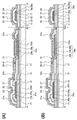
도 3은 반도체 장치의 일 형태를 설명하는 단면도이다.
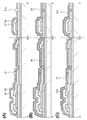
도 4는 반도체 장치의 제작 방법의 일 형태를 설명하는 단면도이다.
도 5는 반도체 장치의 제작 방법의 일 형태를 설명하는 단면도이다.
도 6은 반도체 장치의 제작 방법의 일 형태를 설명하는 단면도이다.
도 7은 반도체 장치의 제작 방법의 일 형태를 설명하는 단면도이다.
도 8은 반도체 장치의 일 형태를 설명하는 상면도이다.
도 9는 반도체 장치의 제작 방법의 일 형태를 설명하는 단면도이다.
도 10은 반도체 장치의 제작 방법의 일 형태를 설명하는 단면도이다.
도 11은 반도체 장치의 제작 방법의 일 형태를 설명하는 단면도이다.
도 12는 반도체 장치의 일 형태를 설명하는 단면도이다.
도 13은 트랜지스터의 밴드 구조를 설명하는 도면이다.
도 14는 반도체 장치의 제작 방법의 일 형태를 설명하는 단면도이다.
도 15는 반도체 장치의 제작 방법의 일 형태를 설명하는 상면도이다.
도 16은 반도체 장치의 일 형태를 설명하는 단면도이다.
도 17은 반도체 장치의 제작 방법의 일 형태를 설명하는 단면도이다.
도 18은 시료의 투과율을 설명하는 도면이다.
도 19는 시료의 시트 저항을 설명하는 도면이다.
도 20은 시료의 구조를 설명하는 도면이다.
도 21은 시료의 시트 저항을 설명하는 도면이다.
도 22는 시료의 시트 저항을 설명하는 도면이다.
도 23은 시료의 구조를 설명하는 도면이다.
도 24는 산화물 반도체막에 포함되는 수소의 농도를 설명하는 도면이다.
도 25는 Vg-Id 특성을 설명하는 도면이다.
도 26은 채널 길이와 문턱 전압의 관계를 설명하는 도면이다.
도 27은 실시형태에 따른 전자기기의 외관도를 설명하는 도면이다.
도 28은 표시 모듈을 설명하는 도면이다.
도 29는 반도체 장치의 일 형태를 설명하는 단면도이다.
도 30은 반도체 장치의 일 형태를 설명하는 상면도이다.
도 31은 저항율의 온도 의존성을 설명하는 도면이다.

12:도전막
13:도전막
15:질화물 절연막
16:산화물 절연막
16c:산화물 반도체막
17:산화물 절연막
18:산화물 반도체막
19a:산화물 반도체막
19b:막
19c:산화물 반도체막
20:도전막
21a:도전막
21b:도전막
21c:도전막
22:산화물 절연막
23:산화물 절연막
24:산화물 절연막
25:산화물 절연막
26:금속막
26a:금속 산화물막
27:금속 산화물막
27a:금속 산화물막
27b:금속 산화물막
28:질화물 절연막
29:질화물 절연막
30:도전막
31:도전막
31a:도전막
31b:슬릿
32:산화물 반도체막
37a:다층막
37b:다층막
38a:다층막
38b:다층막
39a:산화물 반도체막
39b:막
41:개구부
41a:개구부
49a:산화물 반도체막
49b:막
101:화소부
102:트랜지스터
102a:트랜지스터
102b:트랜지스터
102c:트랜지스터
103:화소
104:주사선 구동 회로
105:용량 소자
105a:용량 소자
105b:용량 소자
105c:용량 소자
106:신호선 구동 회로
107:주사선
109:신호선
113:금속 산화물막
115:용량선
121:액정 소자
131:발광 소자
133:트랜지스터
135:트랜지스터
137:배선
139:배선
141:배선
801:유리 기판
803:산화물 반도체막
805:금속막
811:유리 기판
813:산화물 반도체막
815:금속 산화물막
821:유리 기판
823:산화물 반도체막
825:금속 산화물막
827:질화물 절연막
831:유리 기판
833:산화물 반도체막
835:질화물 절연막
1001:본체
1002:하우징
1003a:표시부
1003b:표시부
1004:키보드 버튼
1021:본체
1022:고정부
1023:표시부
1024:조작 버튼
1025:외부 메모리 슬롯
1030:하우징
1031:하우징
1032:표시 패널
1033:스피커
1034:마이크로폰
1035:조작 키
1036:포인팅 디바이스
1037:카메라 렌즈
1038:외부 접속 단자
1040:태양전지
1041:외부 메모리 슬롯
1050:텔레비전 장치
1051:하우징
1052:기억 매체 재생 녹화부
1053:표시부
1054:외부 접속 단자
1055:스탠드
1056:외부 메모리
1901:유리 기판
1903:절연막
1904:절연막
1905:산화물 반도체막
1907:도전막
1909:도전막
1910:절연막
1911:절연막
1912:금속 산화물막
1913:개구부
1914:개구부
1915:개구부
8000:표시 모듈
8001:상부 커버
8002:하부 커버
8003:FPC
8004:터치 패널
8005:FPC
8006:표시 패널
8007:백 라이트 유닛
8008:광원
8009:프레임
8010:프린트 기판
8011:배터리
Claims (20)
- 반도체 장치에 있어서:
트랜지스터로서:
절연 표면상에 채널 영역을 포함하는 산화물 반도체막; 및
상기 산화물 반도체막에 전기적으로 접속된 소스 전극 및 드레인 전극을 포함하는, 상기 트랜지스터;
상기 채널 영역, 상기 소스 전극, 및 상기 드레인 전극 위에 있고 상기 채널 영역, 상기 소스 전극, 및 상기 드레인 전극과 접촉하는 산화물 절연막;
상기 산화물 절연막 위의 금속 산화물막;
상기 금속 산화물막 위의 투광성을 갖는 도전막; 및
용량 소자로서:
상기 절연 표면상의 제 1 전극;
상기 제 1 전극 위에 있고 상기 제 1 전극과 접촉하는 상기 금속 산화물막; 및
상기 금속 산화물막 위의 제 2 전극으로서 상기 투광성을 갖는 도전막을 포함하는, 상기 용량 소자를 포함하고,
상기 산화물 반도체막과 상기 제 1 전극은 같은 재료를 함유하고,
상기 용량 소자에서, 상기 산화물 절연막이 상기 제 1 전극과 상기 금속 산화물막 사이에 제공되지 않는, 반도체 장치. - 반도체 장치에 있어서:
트랜지스터로서:
절연 표면상에 채널 영역을 포함하는 산화물 반도체막; 및
상기 산화물 반도체막에 전기적으로 접속된 소스 전극 및 드레인 전극을 포함하는, 상기 트랜지스터;
상기 채널 영역, 상기 소스 전극, 및 상기 드레인 전극 위에 있고 상기 채널 영역, 상기 소스 전극, 및 상기 드레인 전극과 접촉하는 산화물 절연막;
상기 산화물 절연막 위의 금속 산화물막;
상기 금속 산화물막 위의 질화물 절연막;
상기 질화물 절연막 위의 투광성을 갖는 도전막; 및
용량 소자로서:
상기 절연 표면상의 제 1 전극;
상기 제 1 전극 위에 있고 상기 제 1 전극과 접촉하는 상기 금속 산화물막;
상기 금속 산화물막 위의 상기 질화물 절연막; 및
상기 질화물 절연막 위의 제 2 전극으로서 상기 투광성을 갖는 도전막을 포함하는, 상기 용량 소자를 포함하고,
상기 산화물 반도체막과 상기 제 1 전극은 같은 재료를 함유하고,
상기 용량 소자에서, 상기 산화물 절연막이 상기 제 1 전극과 상기 금속 산화물막 사이에 제공되지 않는, 반도체 장치. - 삭제
- 삭제
- 삭제
- 제 1 항 또는 제 2 항에 있어서,
상기 산화물 반도체막과 상기 제 1 전극은 각각 인듐과, 알루미늄, 갈륨, 이트륨, 지르코늄, 란타넘, 세륨, 및 네오디뮴으로부터 선택된 금속 원소를 함유하는, 반도체 장치. - 제 1 항 또는 제 2 항에 있어서,
상기 금속 산화물막은 산화 알루미늄, 산화 질화 알루미늄, 산화 갈륨, 산화 질화 갈륨, 산화 이트륨, 산화 질화 이트륨, 산화 하프늄, 산화 질화 하프늄, 산화 티탄, 산화 탄탈, 또는 산화 질화 탄탈을 함유하는, 반도체 장치. - 제 1 항 또는 제 2 항에 있어서,
상기 산화물 반도체막과 상기 제 1 전극은 각각 다층 구조를 가지는, 반도체 장치. - 삭제
- 제 1 항 또는 제 2 항에 있어서,
상기 투광성을 갖는 도전막은 상기 소스 전극 및 상기 드레인 전극 중 하나에 전기적으로 접속된 화소 전극인, 반도체 장치. - 제 1 항 또는 제 2 항에 있어서,
상기 제 1 전극은 상기 산화물 반도체막보다 높은 수소 농도를 가지는, 반도체 장치. - 제 1 항 또는 제 2 항에 있어서,
상기 제 1 전극은 상기 산화물 반도체막보다 낮은 저항율을 가지는, 반도체 장치. - 삭제
- 삭제
- 삭제
- 삭제
- 삭제
- 삭제
- 삭제
- 삭제
Applications Claiming Priority (4)
| Application Number | Priority Date | Filing Date | Title |
|---|---|---|---|
| JPJP-P-2013-173867 | 2013-08-23 | ||
| JP2013173867 | 2013-08-23 | ||
| JPJP-P-2014-038563 | 2014-02-28 | ||
| JP2014038563 | 2014-02-28 |
Publications (2)
| Publication Number | Publication Date |
|---|---|
| KR20150022676A KR20150022676A (ko) | 2015-03-04 |
| KR102244553B1 true KR102244553B1 (ko) | 2021-04-23 |
Family
ID=52479561
Family Applications (1)
| Application Number | Title | Priority Date | Filing Date |
|---|---|---|---|
| KR1020140105443A Active KR102244553B1 (ko) | 2013-08-23 | 2014-08-13 | 용량 소자 및 반도체 장치 |
Country Status (3)
| Country | Link |
|---|---|
| US (1) | US10134781B2 (ko) |
| JP (6) | JP6426942B2 (ko) |
| KR (1) | KR102244553B1 (ko) |
Families Citing this family (15)
| Publication number | Priority date | Publication date | Assignee | Title |
|---|---|---|---|---|
| PT3321262T (pt) | 2012-03-01 | 2021-03-04 | Array Biopharma Inc | Inibidores de serina/treonina quinases |
| JP2015179247A (ja) | 2013-10-22 | 2015-10-08 | 株式会社半導体エネルギー研究所 | 表示装置 |
| JP2016027597A (ja) * | 2013-12-06 | 2016-02-18 | 株式会社半導体エネルギー研究所 | 半導体装置 |
| US9753590B2 (en) * | 2014-06-13 | 2017-09-05 | Lg Display Co., Ltd. | Display device integrated with touch screen panel and method of fabricating the same |
| CN104319279B (zh) * | 2014-11-10 | 2017-11-14 | 京东方科技集团股份有限公司 | 阵列基板及其制造方法、显示装置 |
| US9964799B2 (en) | 2015-03-17 | 2018-05-08 | Semiconductor Energy Laboratory Co., Ltd. | Display device, display module, and electronic device |
| US9837547B2 (en) * | 2015-05-22 | 2017-12-05 | Semiconductor Energy Laboratory Co., Ltd. | Semiconductor device comprising oxide conductor and display device including the semiconductor device |
| US9947895B2 (en) * | 2015-06-17 | 2018-04-17 | Universal Display Corporation | Flexible AMOLED display |
| US9852926B2 (en) * | 2015-10-20 | 2017-12-26 | Semiconductor Energy Laboratory Co., Ltd. | Manufacturing method for semiconductor device |
| US10700212B2 (en) * | 2016-01-28 | 2020-06-30 | Semiconductor Energy Laboratory Co., Ltd. | Semiconductor device, semiconductor wafer, module, electronic device, and manufacturing method thereof |
| TWI611463B (zh) * | 2016-06-29 | 2018-01-11 | 友達光電股份有限公司 | 金屬氧化物半導體層的結晶方法及半導體結構 |
| US10205008B2 (en) * | 2016-08-03 | 2019-02-12 | Semiconductor Energy Laboratory Co., Ltd. | Manufacturing method of semiconductor device |
| CN117116946A (zh) * | 2017-05-19 | 2023-11-24 | 株式会社半导体能源研究所 | 半导体装置、显示装置以及半导体装置的制造方法 |
| CN110164878B (zh) * | 2019-06-10 | 2022-05-03 | 惠科股份有限公司 | 阵列基板及其制备方法 |
| CN113470988B (zh) * | 2021-07-08 | 2022-03-04 | 齐鲁工业大学 | 一种缺陷调控的镓氧氮化物@碳布工作电极及其用途 |
Citations (4)
| Publication number | Priority date | Publication date | Assignee | Title |
|---|---|---|---|---|
| JP2007123297A (ja) * | 2005-10-24 | 2007-05-17 | Sharp Corp | 半導体装置及びその製造方法 |
| WO2012086513A1 (ja) * | 2010-12-20 | 2012-06-28 | シャープ株式会社 | 半導体装置および表示装置 |
| JP2013004958A (ja) * | 2011-06-14 | 2013-01-07 | Samsung Electronics Co Ltd | 薄膜トランジスタ、薄膜トランジスタパネル、及びこれらを製造する方法 |
| JP2013110397A (ja) * | 2011-10-24 | 2013-06-06 | Semiconductor Energy Lab Co Ltd | 半導体装置及び半導体装置の作製方法 |
Family Cites Families (161)
| Publication number | Priority date | Publication date | Assignee | Title |
|---|---|---|---|---|
| JPS60198861A (ja) | 1984-03-23 | 1985-10-08 | Fujitsu Ltd | 薄膜トランジスタ |
| JPH0244256B2 (ja) | 1987-01-28 | 1990-10-03 | Kagaku Gijutsucho Mukizaishitsu Kenkyushocho | Ingazn2o5deshimesarerurotsuhoshokeinosojokozoojusurukagobutsuoyobisonoseizoho |
| JPS63210023A (ja) | 1987-02-24 | 1988-08-31 | Natl Inst For Res In Inorg Mater | InGaZn↓4O↓7で示される六方晶系の層状構造を有する化合物およびその製造法 |
| JPH0244260B2 (ja) | 1987-02-24 | 1990-10-03 | Kagaku Gijutsucho Mukizaishitsu Kenkyushocho | Ingazn5o8deshimesarerurotsuhoshokeinosojokozoojusurukagobutsuoyobisonoseizoho |
| JPH0244258B2 (ja) | 1987-02-24 | 1990-10-03 | Kagaku Gijutsucho Mukizaishitsu Kenkyushocho | Ingazn3o6deshimesarerurotsuhoshokeinosojokozoojusurukagobutsuoyobisonoseizoho |
| JPH0244262B2 (ja) | 1987-02-27 | 1990-10-03 | Kagaku Gijutsucho Mukizaishitsu Kenkyushocho | Ingazn6o9deshimesarerurotsuhoshokeinosojokozoojusurukagobutsuoyobisonoseizoho |
| JPH0244263B2 (ja) | 1987-04-22 | 1990-10-03 | Kagaku Gijutsucho Mukizaishitsu Kenkyushocho | Ingazn7o10deshimesarerurotsuhoshokeinosojokozoojusurukagobutsuoyobisonoseizoho |
| JPH05251705A (ja) | 1992-03-04 | 1993-09-28 | Fuji Xerox Co Ltd | 薄膜トランジスタ |
| JPH07104312A (ja) | 1993-09-30 | 1995-04-21 | Sanyo Electric Co Ltd | 液晶表示装置の製造方法 |
| JP3479375B2 (ja) | 1995-03-27 | 2003-12-15 | 科学技術振興事業団 | 亜酸化銅等の金属酸化物半導体による薄膜トランジスタとpn接合を形成した金属酸化物半導体装置およびそれらの製造方法 |
| EP0820644B1 (en) | 1995-08-03 | 2005-08-24 | Koninklijke Philips Electronics N.V. | Semiconductor device provided with transparent switching element |
| JP3625598B2 (ja) | 1995-12-30 | 2005-03-02 | 三星電子株式会社 | 液晶表示装置の製造方法 |
| JP4170454B2 (ja) | 1998-07-24 | 2008-10-22 | Hoya株式会社 | 透明導電性酸化物薄膜を有する物品及びその製造方法 |
| JP2000150861A (ja) | 1998-11-16 | 2000-05-30 | Tdk Corp | 酸化物薄膜 |
| JP3276930B2 (ja) | 1998-11-17 | 2002-04-22 | 科学技術振興事業団 | トランジスタ及び半導体装置 |
| JP3683463B2 (ja) * | 1999-03-11 | 2005-08-17 | シャープ株式会社 | アクティブマトリクス基板、その製造方法、及び、該基板を用いたイメージセンサ |
| TW460731B (en) | 1999-09-03 | 2001-10-21 | Ind Tech Res Inst | Electrode structure and production method of wide viewing angle LCD |
| JP4089858B2 (ja) | 2000-09-01 | 2008-05-28 | 国立大学法人東北大学 | 半導体デバイス |
| JP3931547B2 (ja) | 2000-10-18 | 2007-06-20 | セイコーエプソン株式会社 | 電気光学装置及びその製造方法 |
| KR20020038482A (ko) | 2000-11-15 | 2002-05-23 | 모리시타 요이찌 | 박막 트랜지스터 어레이, 그 제조방법 및 그것을 이용한표시패널 |
| JP3997731B2 (ja) | 2001-03-19 | 2007-10-24 | 富士ゼロックス株式会社 | 基材上に結晶性半導体薄膜を形成する方法 |
| JP2002289859A (ja) | 2001-03-23 | 2002-10-04 | Minolta Co Ltd | 薄膜トランジスタ |
| JP3925839B2 (ja) | 2001-09-10 | 2007-06-06 | シャープ株式会社 | 半導体記憶装置およびその試験方法 |
| JP4090716B2 (ja) | 2001-09-10 | 2008-05-28 | 雅司 川崎 | 薄膜トランジスタおよびマトリクス表示装置 |
| JP4164562B2 (ja) | 2002-09-11 | 2008-10-15 | 独立行政法人科学技術振興機構 | ホモロガス薄膜を活性層として用いる透明薄膜電界効果型トランジスタ |
| US7061014B2 (en) | 2001-11-05 | 2006-06-13 | Japan Science And Technology Agency | Natural-superlattice homologous single crystal thin film, method for preparation thereof, and device using said single crystal thin film |
| JP4083486B2 (ja) | 2002-02-21 | 2008-04-30 | 独立行政法人科学技術振興機構 | LnCuO(S,Se,Te)単結晶薄膜の製造方法 |
| CN1445821A (zh) | 2002-03-15 | 2003-10-01 | 三洋电机株式会社 | ZnO膜和ZnO半导体层的形成方法、半导体元件及其制造方法 |
| JP3933591B2 (ja) | 2002-03-26 | 2007-06-20 | 淳二 城戸 | 有機エレクトロルミネッセント素子 |
| US7339187B2 (en) | 2002-05-21 | 2008-03-04 | State Of Oregon Acting By And Through The Oregon State Board Of Higher Education On Behalf Of Oregon State University | Transistor structures |
| US7187031B2 (en) | 2002-05-31 | 2007-03-06 | Sharp Kabushiki Kaisha | Semiconductor device having a low dielectric constant film and manufacturing method thereof |
| JP2004022625A (ja) | 2002-06-13 | 2004-01-22 | Murata Mfg Co Ltd | 半導体デバイス及び該半導体デバイスの製造方法 |
| US7105868B2 (en) | 2002-06-24 | 2006-09-12 | Cermet, Inc. | High-electron mobility transistor with zinc oxide |
| US7067843B2 (en) | 2002-10-11 | 2006-06-27 | E. I. Du Pont De Nemours And Company | Transparent oxide semiconductor thin film transistors |
| JP4166105B2 (ja) | 2003-03-06 | 2008-10-15 | シャープ株式会社 | 半導体装置およびその製造方法 |
| JP2004273732A (ja) | 2003-03-07 | 2004-09-30 | Sharp Corp | アクティブマトリクス基板およびその製造方法 |
| JP4108633B2 (ja) | 2003-06-20 | 2008-06-25 | シャープ株式会社 | 薄膜トランジスタおよびその製造方法ならびに電子デバイス |
| US7262463B2 (en) | 2003-07-25 | 2007-08-28 | Hewlett-Packard Development Company, L.P. | Transistor including a deposited channel region having a doped portion |
| JP4483235B2 (ja) | 2003-09-01 | 2010-06-16 | カシオ計算機株式会社 | トランジスタアレイ基板の製造方法及びトランジスタアレイ基板 |
| US7145174B2 (en) | 2004-03-12 | 2006-12-05 | Hewlett-Packard Development Company, Lp. | Semiconductor device |
| US7297977B2 (en) | 2004-03-12 | 2007-11-20 | Hewlett-Packard Development Company, L.P. | Semiconductor device |
| EP2226847B1 (en) | 2004-03-12 | 2017-02-08 | Japan Science And Technology Agency | Amorphous oxide and thin film transistor |
| US7282782B2 (en) | 2004-03-12 | 2007-10-16 | Hewlett-Packard Development Company, L.P. | Combined binary oxide semiconductor device |
| US7211825B2 (en) | 2004-06-14 | 2007-05-01 | Yi-Chi Shih | Indium oxide-based thin film transistors and circuits |
| JP2006100760A (ja) | 2004-09-02 | 2006-04-13 | Casio Comput Co Ltd | 薄膜トランジスタおよびその製造方法 |
| US7285501B2 (en) | 2004-09-17 | 2007-10-23 | Hewlett-Packard Development Company, L.P. | Method of forming a solution processed device |
| US7298084B2 (en) | 2004-11-02 | 2007-11-20 | 3M Innovative Properties Company | Methods and displays utilizing integrated zinc oxide row and column drivers in conjunction with organic light emitting diodes |
| JP5118811B2 (ja) | 2004-11-10 | 2013-01-16 | キヤノン株式会社 | 発光装置及び表示装置 |
| JP5126729B2 (ja) | 2004-11-10 | 2013-01-23 | キヤノン株式会社 | 画像表示装置 |
| US7863611B2 (en) | 2004-11-10 | 2011-01-04 | Canon Kabushiki Kaisha | Integrated circuits utilizing amorphous oxides |
| US7791072B2 (en) | 2004-11-10 | 2010-09-07 | Canon Kabushiki Kaisha | Display |
| RU2358355C2 (ru) | 2004-11-10 | 2009-06-10 | Кэнон Кабусики Кайся | Полевой транзистор |
| US7453065B2 (en) | 2004-11-10 | 2008-11-18 | Canon Kabushiki Kaisha | Sensor and image pickup device |
| US7829444B2 (en) | 2004-11-10 | 2010-11-09 | Canon Kabushiki Kaisha | Field effect transistor manufacturing method |
| EP2455975B1 (en) | 2004-11-10 | 2015-10-28 | Canon Kabushiki Kaisha | Field effect transistor with amorphous oxide |
| US7579224B2 (en) | 2005-01-21 | 2009-08-25 | Semiconductor Energy Laboratory Co., Ltd. | Method for manufacturing a thin film semiconductor device |
| TWI472037B (zh) | 2005-01-28 | 2015-02-01 | Semiconductor Energy Lab | 半導體裝置,電子裝置,和半導體裝置的製造方法 |
| TWI569441B (zh) | 2005-01-28 | 2017-02-01 | 半導體能源研究所股份有限公司 | 半導體裝置,電子裝置,和半導體裝置的製造方法 |
| US7858451B2 (en) | 2005-02-03 | 2010-12-28 | Semiconductor Energy Laboratory Co., Ltd. | Electronic device, semiconductor device and manufacturing method thereof |
| US7948171B2 (en) | 2005-02-18 | 2011-05-24 | Semiconductor Energy Laboratory Co., Ltd. | Light emitting device |
| US20060197092A1 (en) | 2005-03-03 | 2006-09-07 | Randy Hoffman | System and method for forming conductive material on a substrate |
| US8681077B2 (en) | 2005-03-18 | 2014-03-25 | Semiconductor Energy Laboratory Co., Ltd. | Semiconductor device, and display device, driving method and electronic apparatus thereof |
| WO2006105077A2 (en) | 2005-03-28 | 2006-10-05 | Massachusetts Institute Of Technology | Low voltage thin film transistor with high-k dielectric material |
| US7645478B2 (en) | 2005-03-31 | 2010-01-12 | 3M Innovative Properties Company | Methods of making displays |
| US8300031B2 (en) | 2005-04-20 | 2012-10-30 | Semiconductor Energy Laboratory Co., Ltd. | Semiconductor device comprising transistor having gate and drain connected through a current-voltage conversion element |
| JP2006344849A (ja) | 2005-06-10 | 2006-12-21 | Casio Comput Co Ltd | 薄膜トランジスタ |
| US7691666B2 (en) | 2005-06-16 | 2010-04-06 | Eastman Kodak Company | Methods of making thin film transistors comprising zinc-oxide-based semiconductor materials and transistors made thereby |
| US7402506B2 (en) | 2005-06-16 | 2008-07-22 | Eastman Kodak Company | Methods of making thin film transistors comprising zinc-oxide-based semiconductor materials and transistors made thereby |
| US7507618B2 (en) | 2005-06-27 | 2009-03-24 | 3M Innovative Properties Company | Method for making electronic devices using metal oxide nanoparticles |
| KR100711890B1 (ko) | 2005-07-28 | 2007-04-25 | 삼성에스디아이 주식회사 | 유기 발광표시장치 및 그의 제조방법 |
| JP2007059128A (ja) | 2005-08-23 | 2007-03-08 | Canon Inc | 有機el表示装置およびその製造方法 |
| JP2007073705A (ja) | 2005-09-06 | 2007-03-22 | Canon Inc | 酸化物半導体チャネル薄膜トランジスタおよびその製造方法 |
| JP5116225B2 (ja) | 2005-09-06 | 2013-01-09 | キヤノン株式会社 | 酸化物半導体デバイスの製造方法 |
| JP4850457B2 (ja) | 2005-09-06 | 2012-01-11 | キヤノン株式会社 | 薄膜トランジスタ及び薄膜ダイオード |
| JP4280736B2 (ja) | 2005-09-06 | 2009-06-17 | キヤノン株式会社 | 半導体素子 |
| EP1995787A3 (en) | 2005-09-29 | 2012-01-18 | Semiconductor Energy Laboratory Co, Ltd. | Semiconductor device having oxide semiconductor layer and manufacturing method therof |
| JP2007115807A (ja) * | 2005-10-19 | 2007-05-10 | Toppan Printing Co Ltd | トランジスタ |
| JP5037808B2 (ja) | 2005-10-20 | 2012-10-03 | キヤノン株式会社 | アモルファス酸化物を用いた電界効果型トランジスタ、及び該トランジスタを用いた表示装置 |
| CN101577256B (zh) | 2005-11-15 | 2011-07-27 | 株式会社半导体能源研究所 | 半导体器件及其制造方法 |
| TWI292281B (en) | 2005-12-29 | 2008-01-01 | Ind Tech Res Inst | Pixel structure of active organic light emitting diode and method of fabricating the same |
| US7867636B2 (en) | 2006-01-11 | 2011-01-11 | Murata Manufacturing Co., Ltd. | Transparent conductive film and method for manufacturing the same |
| JP4977478B2 (ja) | 2006-01-21 | 2012-07-18 | 三星電子株式会社 | ZnOフィルム及びこれを用いたTFTの製造方法 |
| US7576394B2 (en) | 2006-02-02 | 2009-08-18 | Kochi Industrial Promotion Center | Thin film transistor including low resistance conductive thin films and manufacturing method thereof |
| JP5015471B2 (ja) | 2006-02-15 | 2012-08-29 | 財団法人高知県産業振興センター | 薄膜トランジスタ及びその製法 |
| US7977169B2 (en) | 2006-02-15 | 2011-07-12 | Kochi Industrial Promotion Center | Semiconductor device including active layer made of zinc oxide with controlled orientations and manufacturing method thereof |
| EP1843194A1 (en) | 2006-04-06 | 2007-10-10 | Semiconductor Energy Laboratory Co., Ltd. | Liquid crystal display device, semiconductor device, and electronic appliance |
| KR20070101595A (ko) | 2006-04-11 | 2007-10-17 | 삼성전자주식회사 | ZnO TFT |
| US20070252928A1 (en) | 2006-04-28 | 2007-11-01 | Toppan Printing Co., Ltd. | Structure, transmission type liquid crystal display, reflection type display and manufacturing method thereof |
| JP5028033B2 (ja) | 2006-06-13 | 2012-09-19 | キヤノン株式会社 | 酸化物半導体膜のドライエッチング方法 |
| JP4609797B2 (ja) | 2006-08-09 | 2011-01-12 | Nec液晶テクノロジー株式会社 | 薄膜デバイス及びその製造方法 |
| JP4999400B2 (ja) | 2006-08-09 | 2012-08-15 | キヤノン株式会社 | 酸化物半導体膜のドライエッチング方法 |
| JP4332545B2 (ja) | 2006-09-15 | 2009-09-16 | キヤノン株式会社 | 電界効果型トランジスタ及びその製造方法 |
| JP5164357B2 (ja) | 2006-09-27 | 2013-03-21 | キヤノン株式会社 | 半導体装置及び半導体装置の製造方法 |
| JP4274219B2 (ja) | 2006-09-27 | 2009-06-03 | セイコーエプソン株式会社 | 電子デバイス、有機エレクトロルミネッセンス装置、有機薄膜半導体装置 |
| US7622371B2 (en) | 2006-10-10 | 2009-11-24 | Hewlett-Packard Development Company, L.P. | Fused nanocrystal thin film semiconductor and method |
| US7772021B2 (en) | 2006-11-29 | 2010-08-10 | Samsung Electronics Co., Ltd. | Flat panel displays comprising a thin-film transistor having a semiconductive oxide in its channel and methods of fabricating the same for use in flat panel displays |
| JP2008140684A (ja) | 2006-12-04 | 2008-06-19 | Toppan Printing Co Ltd | カラーelディスプレイおよびその製造方法 |
| KR101303578B1 (ko) | 2007-01-05 | 2013-09-09 | 삼성전자주식회사 | 박막 식각 방법 |
| US8207063B2 (en) | 2007-01-26 | 2012-06-26 | Eastman Kodak Company | Process for atomic layer deposition |
| KR100851215B1 (ko) | 2007-03-14 | 2008-08-07 | 삼성에스디아이 주식회사 | 박막 트랜지스터 및 이를 이용한 유기 전계 발광표시장치 |
| US7795613B2 (en) | 2007-04-17 | 2010-09-14 | Toppan Printing Co., Ltd. | Structure with transistor |
| KR101325053B1 (ko) | 2007-04-18 | 2013-11-05 | 삼성디스플레이 주식회사 | 박막 트랜지스터 기판 및 이의 제조 방법 |
| KR20080094300A (ko) | 2007-04-19 | 2008-10-23 | 삼성전자주식회사 | 박막 트랜지스터 및 그 제조 방법과 박막 트랜지스터를포함하는 평판 디스플레이 |
| KR101334181B1 (ko) | 2007-04-20 | 2013-11-28 | 삼성전자주식회사 | 선택적으로 결정화된 채널층을 갖는 박막 트랜지스터 및 그제조 방법 |
| US8274078B2 (en) | 2007-04-25 | 2012-09-25 | Canon Kabushiki Kaisha | Metal oxynitride semiconductor containing zinc |
| JP5044273B2 (ja) | 2007-04-27 | 2012-10-10 | 三菱電機株式会社 | 薄膜トランジスタアレイ基板、その製造方法、及び表示装置 |
| KR101345376B1 (ko) | 2007-05-29 | 2013-12-24 | 삼성전자주식회사 | ZnO 계 박막 트랜지스터 및 그 제조방법 |
| JP4759598B2 (ja) | 2007-09-28 | 2011-08-31 | キヤノン株式会社 | 薄膜トランジスタ、その製造方法及びそれを用いた表示装置 |
| JP2009099887A (ja) | 2007-10-19 | 2009-05-07 | Hitachi Displays Ltd | 表示装置 |
| KR101375831B1 (ko) * | 2007-12-03 | 2014-04-02 | 삼성전자주식회사 | 산화물 반도체 박막 트랜지스터를 이용한 디스플레이 장치 |
| JP5215158B2 (ja) | 2007-12-17 | 2013-06-19 | 富士フイルム株式会社 | 無機結晶性配向膜及びその製造方法、半導体デバイス |
| JP5584960B2 (ja) | 2008-07-03 | 2014-09-10 | ソニー株式会社 | 薄膜トランジスタおよび表示装置 |
| JP4623179B2 (ja) | 2008-09-18 | 2011-02-02 | ソニー株式会社 | 薄膜トランジスタおよびその製造方法 |
| JP5451280B2 (ja) | 2008-10-09 | 2014-03-26 | キヤノン株式会社 | ウルツ鉱型結晶成長用基板およびその製造方法ならびに半導体装置 |
| JP2010129742A (ja) * | 2008-11-27 | 2010-06-10 | Konica Minolta Holdings Inc | 電子デバイス及びその製造方法 |
| JP5491833B2 (ja) | 2008-12-05 | 2014-05-14 | 株式会社半導体エネルギー研究所 | 半導体装置 |
| EP2515337B1 (en) * | 2008-12-24 | 2016-02-24 | Semiconductor Energy Laboratory Co., Ltd. | Driver circuit and semiconductor device |
| JP2010243594A (ja) * | 2009-04-01 | 2010-10-28 | Sharp Corp | 薄膜トランジスタ基板およびその製造方法 |
| EP2256814B1 (en) | 2009-05-29 | 2019-01-16 | Semiconductor Energy Laboratory Co, Ltd. | Oxide semiconductor device and method for manufacturing the same |
| KR102216028B1 (ko) | 2009-07-10 | 2021-02-16 | 가부시키가이샤 한도오따이 에네루기 켄큐쇼 | 반도체 장치 및 그 제조 방법 |
| WO2011043194A1 (en) * | 2009-10-09 | 2011-04-14 | Semiconductor Energy Laboratory Co., Ltd. | Semiconductor device and method for manufacturing the same |
| KR101801959B1 (ko) * | 2009-10-21 | 2017-11-27 | 가부시키가이샤 한도오따이 에네루기 켄큐쇼 | 액정 표시 장치 및 그 액정 표시 장치를 구비하는 전자기기 |
| WO2011068021A1 (en) * | 2009-12-04 | 2011-06-09 | Semiconductor Energy Laboratory Co., Ltd. | Display device |
| US8685803B2 (en) * | 2009-12-09 | 2014-04-01 | Sharp Kabushiki Kaisha | Semiconductor device and method for producing same |
| JP2011138934A (ja) | 2009-12-28 | 2011-07-14 | Sony Corp | 薄膜トランジスタ、表示装置および電子機器 |
| JP5133468B2 (ja) | 2010-05-24 | 2013-01-30 | シャープ株式会社 | 薄膜トランジスタ基板及びその製造方法 |
| US8558960B2 (en) * | 2010-09-13 | 2013-10-15 | Semiconductor Energy Laboratory Co., Ltd. | Liquid crystal display device and method for manufacturing the same |
| US9230994B2 (en) * | 2010-09-15 | 2016-01-05 | Semiconductor Energy Laboratory Co., Ltd. | Liquid crystal display device |
| TWI432865B (zh) | 2010-12-01 | 2014-04-01 | Au Optronics Corp | 畫素結構及其製作方法 |
| KR102100425B1 (ko) | 2011-12-27 | 2020-04-13 | 가부시키가이샤 한도오따이 에네루기 켄큐쇼 | 반도체 장치 및 반도체 장치의 제작 방법 |
| CN102651401B (zh) | 2011-12-31 | 2015-03-18 | 京东方科技集团股份有限公司 | 一种薄膜晶体管、阵列基板及其制造方法和显示器件 |
| US20140014948A1 (en) | 2012-07-12 | 2014-01-16 | Semiconductor Energy Laboratory Co. Ltd. | Semiconductor device |
| DE112013007566B3 (de) | 2012-08-03 | 2018-02-22 | Semiconductor Energy Laboratory Co., Ltd. | Halbleitervorrichtung |
| US8937307B2 (en) | 2012-08-10 | 2015-01-20 | Semiconductor Energy Laboratory Co., Ltd. | Semiconductor device |
| JP2014199899A (ja) | 2012-08-10 | 2014-10-23 | 株式会社半導体エネルギー研究所 | 半導体装置 |
| DE102013216824B4 (de) | 2012-08-28 | 2024-10-17 | Semiconductor Energy Laboratory Co., Ltd. | Halbleitervorrichtung |
| TWI657539B (zh) | 2012-08-31 | 2019-04-21 | 日商半導體能源研究所股份有限公司 | 半導體裝置 |
| US9535277B2 (en) | 2012-09-05 | 2017-01-03 | Semiconductor Energy Laboratory Co., Ltd. | Conductive oxide film, display device, and method for forming conductive oxide film |
| KR102691397B1 (ko) | 2012-09-13 | 2024-08-05 | 가부시키가이샤 한도오따이 에네루기 켄큐쇼 | 표시 장치 |
| US9018624B2 (en) | 2012-09-13 | 2015-04-28 | Semiconductor Energy Laboratory Co., Ltd. | Display device and electronic appliance |
| US8981372B2 (en) | 2012-09-13 | 2015-03-17 | Semiconductor Energy Laboratory Co., Ltd. | Display device and electronic appliance |
| US8927985B2 (en) | 2012-09-20 | 2015-01-06 | Semiconductor Energy Laboratory Co., Ltd. | Semiconductor device |
| KR101954984B1 (ko) * | 2012-09-25 | 2019-03-08 | 삼성디스플레이 주식회사 | 박막 트랜지스터 어레이 기판, 이를 포함하는 유기 발광 표시 장치 및 그 제조 방법 |
| US9905585B2 (en) | 2012-12-25 | 2018-02-27 | Semiconductor Energy Laboratory Co., Ltd. | Semiconductor device comprising capacitor |
| KR102209871B1 (ko) | 2012-12-25 | 2021-02-01 | 가부시키가이샤 한도오따이 에네루기 켄큐쇼 | 반도체 장치 |
| KR102241249B1 (ko) | 2012-12-25 | 2021-04-15 | 가부시키가이샤 한도오따이 에네루기 켄큐쇼 | 저항 소자, 표시 장치, 및 전자기기 |
| TWI607510B (zh) * | 2012-12-28 | 2017-12-01 | 半導體能源研究所股份有限公司 | 半導體裝置及半導體裝置的製造方法 |
| KR102770182B1 (ko) | 2012-12-28 | 2025-02-18 | 가부시키가이샤 한도오따이 에네루기 켄큐쇼 | 반도체 장치, 및 반도체 장치의 제작 방법 |
| US8981374B2 (en) | 2013-01-30 | 2015-03-17 | Semiconductor Energy Laboratory Co., Ltd. | Semiconductor device |
| TWI611567B (zh) | 2013-02-27 | 2018-01-11 | 半導體能源研究所股份有限公司 | 半導體裝置、驅動電路及顯示裝置 |
| TWI635613B (zh) | 2013-04-03 | 2018-09-11 | 半導體能源研究所股份有限公司 | 半導體裝置 |
| US20140306219A1 (en) | 2013-04-10 | 2014-10-16 | Semiconductor Energy Laboratory Co., Ltd. | Semiconductor device |
| JP6456598B2 (ja) | 2013-04-19 | 2019-01-23 | 株式会社半導体エネルギー研究所 | 表示装置 |
| US9915848B2 (en) | 2013-04-19 | 2018-03-13 | Semiconductor Energy Laboratory Co., Ltd. | Display device and electronic device |
| US9231002B2 (en) | 2013-05-03 | 2016-01-05 | Semiconductor Energy Laboratory Co., Ltd. | Display device and electronic device |
| US9704894B2 (en) | 2013-05-10 | 2017-07-11 | Semiconductor Energy Laboratory Co., Ltd. | Display device including pixel electrode including oxide |
| TW202414844A (zh) | 2013-05-16 | 2024-04-01 | 日商半導體能源研究所股份有限公司 | 半導體裝置 |
| JP6475424B2 (ja) | 2013-06-05 | 2019-02-27 | 株式会社半導体エネルギー研究所 | 半導体装置 |
| TWI687748B (zh) | 2013-06-05 | 2020-03-11 | 日商半導體能源研究所股份有限公司 | 顯示裝置及電子裝置 |
| US9293480B2 (en) | 2013-07-10 | 2016-03-22 | Semiconductor Energy Laboratory Co., Ltd. | Semiconductor device and display device including the semiconductor device |
| US9818763B2 (en) | 2013-07-12 | 2017-11-14 | Semiconductor Energy Laboratory Co., Ltd. | Display device and method for manufacturing display device |
-
2014
- 2014-08-13 KR KR1020140105443A patent/KR102244553B1/ko active Active
- 2014-08-19 US US14/462,994 patent/US10134781B2/en active Active
- 2014-08-21 JP JP2014168105A patent/JP6426942B2/ja not_active Expired - Fee Related
-
2018
- 2018-10-26 JP JP2018201457A patent/JP2019057713A/ja not_active Withdrawn
-
2020
- 2020-10-01 JP JP2020166932A patent/JP7038777B2/ja active Active
-
2022
- 2022-03-08 JP JP2022035274A patent/JP7364721B2/ja active Active
-
2023
- 2023-10-05 JP JP2023173508A patent/JP7516641B2/ja active Active
-
2024
- 2024-07-03 JP JP2024107301A patent/JP7689232B2/ja active Active
Patent Citations (4)
| Publication number | Priority date | Publication date | Assignee | Title |
|---|---|---|---|---|
| JP2007123297A (ja) * | 2005-10-24 | 2007-05-17 | Sharp Corp | 半導体装置及びその製造方法 |
| WO2012086513A1 (ja) * | 2010-12-20 | 2012-06-28 | シャープ株式会社 | 半導体装置および表示装置 |
| JP2013004958A (ja) * | 2011-06-14 | 2013-01-07 | Samsung Electronics Co Ltd | 薄膜トランジスタ、薄膜トランジスタパネル、及びこれらを製造する方法 |
| JP2013110397A (ja) * | 2011-10-24 | 2013-06-06 | Semiconductor Energy Lab Co Ltd | 半導体装置及び半導体装置の作製方法 |
Also Published As
| Publication number | Publication date |
|---|---|
| US20150053973A1 (en) | 2015-02-26 |
| JP7038777B2 (ja) | 2022-03-18 |
| JP7364721B2 (ja) | 2023-10-18 |
| JP2021013030A (ja) | 2021-02-04 |
| JP2024150485A (ja) | 2024-10-23 |
| JP6426942B2 (ja) | 2018-11-21 |
| JP2019057713A (ja) | 2019-04-11 |
| JP7516641B2 (ja) | 2024-07-16 |
| JP2024001176A (ja) | 2024-01-09 |
| JP2015179810A (ja) | 2015-10-08 |
| JP2022095623A (ja) | 2022-06-28 |
| US10134781B2 (en) | 2018-11-20 |
| KR20150022676A (ko) | 2015-03-04 |
| JP7689232B2 (ja) | 2025-06-05 |
Similar Documents
| Publication | Publication Date | Title |
|---|---|---|
| KR102244553B1 (ko) | 용량 소자 및 반도체 장치 | |
| JP6571255B2 (ja) | 表示装置 | |
| JP7209774B2 (ja) | 半導体装置の作製方法 | |
| TWI688084B (zh) | 顯示裝置 | |
| US11430817B2 (en) | Semiconductor device | |
| TWI657488B (zh) | 半導體裝置、具有該半導體裝置的顯示裝置、具有該顯示裝置的顯示模組以及具有該半導體裝置、該顯示裝置和該顯示模組的電子裝置 | |
| TW201545359A (zh) | 半導體裝置及具有其之顯示裝置 | |
| TW201133640A (en) | Semiconductor device and method for manufacturing the same | |
| TW201510628A (zh) | 顯示裝置 | |
| JP2025014013A (ja) | 液晶表示装置 | |
| JP6392955B2 (ja) | 金属酸化物膜 | |
| JP2018197399A (ja) | 金属酸化物膜及び半導体装置 |
Legal Events
| Date | Code | Title | Description |
|---|---|---|---|
| PA0109 | Patent application |
Patent event code: PA01091R01D Comment text: Patent Application Patent event date: 20140813 |
|
| PG1501 | Laying open of application | ||
| PA0201 | Request for examination |
Patent event code: PA02012R01D Patent event date: 20190809 Comment text: Request for Examination of Application Patent event code: PA02011R01I Patent event date: 20140813 Comment text: Patent Application |
|
| E902 | Notification of reason for refusal | ||
| PE0902 | Notice of grounds for rejection |
Comment text: Notification of reason for refusal Patent event date: 20200709 Patent event code: PE09021S01D |
|
| E701 | Decision to grant or registration of patent right | ||
| PE0701 | Decision of registration |
Patent event code: PE07011S01D Comment text: Decision to Grant Registration Patent event date: 20210122 |
|
| GRNT | Written decision to grant | ||
| PR0701 | Registration of establishment |
Comment text: Registration of Establishment Patent event date: 20210420 Patent event code: PR07011E01D |
|
| PR1002 | Payment of registration fee |
Payment date: 20210420 End annual number: 3 Start annual number: 1 |
|
| PG1601 | Publication of registration | ||
| PR1001 | Payment of annual fee |
Payment date: 20240319 Start annual number: 4 End annual number: 4 |