KR100787423B1 - Organic electroluminescent element - Google Patents
Organic electroluminescent element Download PDFInfo
- Publication number
- KR100787423B1 KR100787423B1 KR1020040089652A KR20040089652A KR100787423B1 KR 100787423 B1 KR100787423 B1 KR 100787423B1 KR 1020040089652 A KR1020040089652 A KR 1020040089652A KR 20040089652 A KR20040089652 A KR 20040089652A KR 100787423 B1 KR100787423 B1 KR 100787423B1
- Authority
- KR
- South Korea
- Prior art keywords
- organic electroluminescent
- electroluminescent device
- unit
- light emitting
- group
- Prior art date
- Legal status (The legal status is an assumption and is not a legal conclusion. Google has not performed a legal analysis and makes no representation as to the accuracy of the status listed.)
- Expired - Lifetime
Links
- 150000001875 compounds Chemical class 0.000 claims abstract description 20
- 239000002019 doping agent Substances 0.000 claims abstract description 16
- 239000000126 substance Substances 0.000 claims abstract description 7
- 125000005647 linker group Chemical group 0.000 claims abstract description 5
- 239000000463 material Substances 0.000 claims description 48
- 238000002347 injection Methods 0.000 claims description 23
- 239000007924 injection Substances 0.000 claims description 23
- 229910052741 iridium Inorganic materials 0.000 claims description 18
- 230000005525 hole transport Effects 0.000 claims description 17
- GKOZUEZYRPOHIO-UHFFFAOYSA-N iridium atom Chemical compound [Ir] GKOZUEZYRPOHIO-UHFFFAOYSA-N 0.000 claims description 17
- 230000000903 blocking effect Effects 0.000 claims description 11
- ZUOUZKKEUPVFJK-UHFFFAOYSA-N diphenyl Chemical compound C1=CC=CC=C1C1=CC=CC=C1 ZUOUZKKEUPVFJK-UHFFFAOYSA-N 0.000 claims description 10
- 238000000034 method Methods 0.000 claims description 10
- 239000007983 Tris buffer Substances 0.000 claims description 9
- 229910052760 oxygen Inorganic materials 0.000 claims description 9
- 125000001997 phenyl group Chemical group [H]C1=C([H])C([H])=C(*)C([H])=C1[H] 0.000 claims description 9
- 229910052717 sulfur Inorganic materials 0.000 claims description 9
- POILWHVDKZOXJZ-ARJAWSKDSA-M (z)-4-oxopent-2-en-2-olate Chemical compound C\C([O-])=C\C(C)=O POILWHVDKZOXJZ-ARJAWSKDSA-M 0.000 claims description 8
- 125000001637 1-naphthyl group Chemical group [H]C1=C([H])C([H])=C2C(*)=C([H])C([H])=C([H])C2=C1[H] 0.000 claims description 8
- -1 2-carbazolylphenyl Chemical group 0.000 claims description 8
- 229910052757 nitrogen Inorganic materials 0.000 claims description 8
- 125000001622 2-naphthyl group Chemical group [H]C1=C([H])C([H])=C2C([H])=C(*)C([H])=C([H])C2=C1[H] 0.000 claims description 7
- 125000003545 alkoxy group Chemical group 0.000 claims description 7
- 125000000217 alkyl group Chemical group 0.000 claims description 7
- 229910052782 aluminium Inorganic materials 0.000 claims description 7
- 125000004432 carbon atom Chemical group C* 0.000 claims description 7
- 239000004305 biphenyl Substances 0.000 claims description 6
- IERDDDBDINUYCD-UHFFFAOYSA-N 1-[4-[4-(9h-carbazol-1-yl)phenyl]phenyl]-9h-carbazole Chemical group C12=CC=CC=C2NC2=C1C=CC=C2C(C=C1)=CC=C1C(C=C1)=CC=C1C1=C2NC3=CC=CC=C3C2=CC=C1 IERDDDBDINUYCD-UHFFFAOYSA-N 0.000 claims description 5
- 235000010290 biphenyl Nutrition 0.000 claims description 5
- 125000003983 fluorenyl group Chemical group C1(=CC=CC=2C3=CC=CC=C3CC12)* 0.000 claims description 4
- UEEXRMUCXBPYOV-UHFFFAOYSA-N iridium;2-phenylpyridine Chemical compound [Ir].C1=CC=CC=C1C1=CC=CC=N1.C1=CC=CC=C1C1=CC=CC=N1.C1=CC=CC=C1C1=CC=CC=N1 UEEXRMUCXBPYOV-UHFFFAOYSA-N 0.000 claims description 4
- NRSBAUDUBWMTGL-UHFFFAOYSA-N 2-(1-benzothiophen-2-yl)pyridine Chemical compound S1C2=CC=CC=C2C=C1C1=CC=CC=N1 NRSBAUDUBWMTGL-UHFFFAOYSA-N 0.000 claims description 3
- XBHOUXSGHYZCNH-UHFFFAOYSA-N 2-phenyl-1,3-benzothiazole Chemical compound C1=CC=CC=C1C1=NC2=CC=CC=C2S1 XBHOUXSGHYZCNH-UHFFFAOYSA-N 0.000 claims description 3
- XAGFODPZIPBFFR-UHFFFAOYSA-N aluminium Chemical compound [Al] XAGFODPZIPBFFR-UHFFFAOYSA-N 0.000 claims description 3
- WECOUKMONWFOGF-UHFFFAOYSA-N 1-[2-[3,5-bis[2-(9h-carbazol-1-yl)-5-methoxyphenyl]phenyl]-4-methoxyphenyl]-9h-carbazole Chemical compound C12=CC=CC=C2NC2=C1C=CC=C2C1=CC=C(OC)C=C1C1=CC(C=2C(=CC=C(OC)C=2)C=2C=3NC4=CC=CC=C4C=3C=CC=2)=CC(C=2C(=CC=C(OC)C=2)C=2C=3NC4=CC=CC=C4C=3C=CC=2)=C1 WECOUKMONWFOGF-UHFFFAOYSA-N 0.000 claims description 2
- AHBDIQVWSLNELJ-UHFFFAOYSA-N 1-[3,5-bis(9h-carbazol-1-yl)phenyl]-9h-carbazole Chemical compound C12=CC=CC=C2NC2=C1C=CC=C2C1=CC(C=2C=3NC4=CC=CC=C4C=3C=CC=2)=CC(C2=C3NC=4C(C3=CC=C2)=CC=CC=4)=C1 AHBDIQVWSLNELJ-UHFFFAOYSA-N 0.000 claims description 2
- XSNBULILWHLFQU-UHFFFAOYSA-N 2,3-dithiophen-2-ylpyridine Chemical compound C1=CSC(C=2C(=NC=CC=2)C=2SC=CC=2)=C1 XSNBULILWHLFQU-UHFFFAOYSA-N 0.000 claims description 2
- RKVIAZWOECXCCM-UHFFFAOYSA-N 2-carbazol-9-yl-n,n-diphenylaniline Chemical compound C1=CC=CC=C1N(C=1C(=CC=CC=1)N1C2=CC=CC=C2C2=CC=CC=C21)C1=CC=CC=C1 RKVIAZWOECXCCM-UHFFFAOYSA-N 0.000 claims description 2
- YAPIJPOCONTNDY-UHFFFAOYSA-N N1C2=CC=CC=C2C2=C1C(C1=CC=C(C=C1)[SiH2]C=1C=CC(=CC=1)C=1C3=C(C4=CC=CC=C4N3)C=CC=1)=CC=C2 Chemical compound N1C2=CC=CC=C2C2=C1C(C1=CC=C(C=C1)[SiH2]C=1C=CC(=CC=1)C=1C3=C(C4=CC=CC=C4N3)C=CC=1)=CC=C2 YAPIJPOCONTNDY-UHFFFAOYSA-N 0.000 claims description 2
- SMWDFEZZVXVKRB-UHFFFAOYSA-N Quinoline Chemical compound N1=CC=CC2=CC=CC=C21 SMWDFEZZVXVKRB-UHFFFAOYSA-N 0.000 claims description 2
- CECAIMUJVYQLKA-UHFFFAOYSA-N iridium 1-phenylisoquinoline Chemical compound [Ir].C1=CC=CC=C1C1=NC=CC2=CC=CC=C12.C1=CC=CC=C1C1=NC=CC2=CC=CC=C12.C1=CC=CC=C1C1=NC=CC2=CC=CC=C12 CECAIMUJVYQLKA-UHFFFAOYSA-N 0.000 claims description 2
- SHNBXKOUKNSCSQ-UHFFFAOYSA-N iridium;1-phenylisoquinoline Chemical compound [Ir].C1=CC=CC=C1C1=NC=CC2=CC=CC=C12.C1=CC=CC=C1C1=NC=CC2=CC=CC=C12 SHNBXKOUKNSCSQ-UHFFFAOYSA-N 0.000 claims description 2
- 229920003227 poly(N-vinyl carbazole) Polymers 0.000 claims description 2
- UHOVQNZJYSORNB-UHFFFAOYSA-N Benzene Chemical compound C1=CC=CC=C1 UHOVQNZJYSORNB-UHFFFAOYSA-N 0.000 claims 3
- JUJWROOIHBZHMG-UHFFFAOYSA-N pyridine Substances C1=CC=NC=C1 JUJWROOIHBZHMG-UHFFFAOYSA-N 0.000 claims 3
- UMJSCPRVCHMLSP-UHFFFAOYSA-N pyridine Natural products COC1=CC=CN=C1 UMJSCPRVCHMLSP-UHFFFAOYSA-N 0.000 claims 3
- QQZMENPYRUUSLY-UHFFFAOYSA-N 1-[4-[3,4-bis(9H-carbazol-1-yl)-5-[1-(9H-carbazol-1-yl)cyclohexa-2,4-dien-1-yl]-2-methylphenyl]-3-methylphenyl]-9H-carbazole Chemical group C1(=CC=CC=2C3=CC=CC=C3NC12)C1(CC=CC=C1)C=1C(=C(C(=C(C1)C1=C(C=C(C=C1)C1=CC=CC=2C3=CC=CC=C3NC12)C)C)C1=CC=CC=2C3=CC=CC=C3NC12)C1=CC=CC=2C3=CC=CC=C3NC12 QQZMENPYRUUSLY-UHFFFAOYSA-N 0.000 claims 1
- 230000005684 electric field Effects 0.000 claims 1
- 239000000758 substrate Substances 0.000 description 8
- RTZKZFJDLAIYFH-UHFFFAOYSA-N Diethyl ether Chemical compound CCOCC RTZKZFJDLAIYFH-UHFFFAOYSA-N 0.000 description 6
- KFZMGEQAYNKOFK-UHFFFAOYSA-N Isopropanol Chemical compound CC(C)O KFZMGEQAYNKOFK-UHFFFAOYSA-N 0.000 description 6
- 230000000052 comparative effect Effects 0.000 description 6
- UJOBWOGCFQCDNV-UHFFFAOYSA-N Carbazole Natural products C1=CC=C2C3=CC=CC=C3NC2=C1 UJOBWOGCFQCDNV-UHFFFAOYSA-N 0.000 description 4
- 230000000694 effects Effects 0.000 description 4
- 238000004770 highest occupied molecular orbital Methods 0.000 description 4
- 238000004768 lowest unoccupied molecular orbital Methods 0.000 description 4
- 238000004519 manufacturing process Methods 0.000 description 4
- 238000004528 spin coating Methods 0.000 description 4
- 230000007704 transition Effects 0.000 description 4
- VQGHOUODWALEFC-UHFFFAOYSA-N 2-phenylpyridine Chemical compound C1=CC=CC=C1C1=CC=CC=N1 VQGHOUODWALEFC-UHFFFAOYSA-N 0.000 description 3
- IBHBKWKFFTZAHE-UHFFFAOYSA-N n-[4-[4-(n-naphthalen-1-ylanilino)phenyl]phenyl]-n-phenylnaphthalen-1-amine Chemical compound C1=CC=CC=C1N(C=1C2=CC=CC=C2C=CC=1)C1=CC=C(C=2C=CC(=CC=2)N(C=2C=CC=CC=2)C=2C3=CC=CC=C3C=CC=2)C=C1 IBHBKWKFFTZAHE-UHFFFAOYSA-N 0.000 description 3
- TVIVIEFSHFOWTE-UHFFFAOYSA-K tri(quinolin-8-yloxy)alumane Chemical compound [Al+3].C1=CN=C2C([O-])=CC=CC2=C1.C1=CN=C2C([O-])=CC=CC2=C1.C1=CN=C2C([O-])=CC=CC2=C1 TVIVIEFSHFOWTE-UHFFFAOYSA-K 0.000 description 3
- 238000001771 vacuum deposition Methods 0.000 description 3
- XLYOFNOQVPJJNP-UHFFFAOYSA-N water Substances O XLYOFNOQVPJJNP-UHFFFAOYSA-N 0.000 description 3
- LPCWDYWZIWDTCV-UHFFFAOYSA-N 1-phenylisoquinoline Chemical compound C1=CC=CC=C1C1=NC=CC2=CC=CC=C12 LPCWDYWZIWDTCV-UHFFFAOYSA-N 0.000 description 2
- MBPCKEZNJVJYTC-UHFFFAOYSA-N 4-[4-(n-phenylanilino)phenyl]aniline Chemical compound C1=CC(N)=CC=C1C1=CC=C(N(C=2C=CC=CC=2)C=2C=CC=CC=2)C=C1 MBPCKEZNJVJYTC-UHFFFAOYSA-N 0.000 description 2
- LFQSCWFLJHTTHZ-UHFFFAOYSA-N Ethanol Chemical compound CCO LFQSCWFLJHTTHZ-UHFFFAOYSA-N 0.000 description 2
- CBENFWSGALASAD-UHFFFAOYSA-N Ozone Chemical compound [O-][O+]=O CBENFWSGALASAD-UHFFFAOYSA-N 0.000 description 2
- FAPWRFPIFSIZLT-UHFFFAOYSA-M Sodium chloride Chemical compound [Na+].[Cl-] FAPWRFPIFSIZLT-UHFFFAOYSA-M 0.000 description 2
- 239000010405 anode material Substances 0.000 description 2
- 239000011575 calcium Substances 0.000 description 2
- 229960004132 diethyl ether Drugs 0.000 description 2
- NIHNNTQXNPWCJQ-UHFFFAOYSA-N fluorene Chemical compound C1=CC=C2CC3=CC=CC=C3C2=C1 NIHNNTQXNPWCJQ-UHFFFAOYSA-N 0.000 description 2
- 239000011521 glass Substances 0.000 description 2
- 239000011777 magnesium Substances 0.000 description 2
- 229910052751 metal Inorganic materials 0.000 description 2
- 239000002184 metal Substances 0.000 description 2
- 238000002156 mixing Methods 0.000 description 2
- 239000000243 solution Substances 0.000 description 2
- 238000002207 thermal evaporation Methods 0.000 description 2
- MNHSTWRXCNIKFM-UHFFFAOYSA-N 1,2-diethyl-9h-fluorene Chemical compound C1=CC=C2C3=CC=C(CC)C(CC)=C3CC2=C1 MNHSTWRXCNIKFM-UHFFFAOYSA-N 0.000 description 1
- CRXBTDWNHVBEIC-UHFFFAOYSA-N 1,2-dimethyl-9h-fluorene Chemical compound C1=CC=C2CC3=C(C)C(C)=CC=C3C2=C1 CRXBTDWNHVBEIC-UHFFFAOYSA-N 0.000 description 1
- QTPLEVOKSWEYAC-UHFFFAOYSA-N 1,2-diphenyl-9h-fluorene Chemical compound C=1C=CC=CC=1C1=C2CC3=CC=CC=C3C2=CC=C1C1=CC=CC=C1 QTPLEVOKSWEYAC-UHFFFAOYSA-N 0.000 description 1
- PRUCJKSKYARXJB-UHFFFAOYSA-N 1-[2-[3,5-bis[2-(9h-carbazol-1-yl)phenyl]phenyl]phenyl]-9h-carbazole Chemical compound C12=CC=CC=C2NC2=C1C=CC=C2C1=CC=CC=C1C1=CC(C=2C(=CC=CC=2)C=2C=3NC4=CC=CC=C4C=3C=CC=2)=CC(C=2C(=CC=CC=2)C=2C=3NC4=CC=CC=C4C=3C=CC=2)=C1 PRUCJKSKYARXJB-UHFFFAOYSA-N 0.000 description 1
- DBDOZRBRAYSLFX-UHFFFAOYSA-N 1-[4-[4-(9h-carbazol-1-yl)-2-methylphenyl]-3-methylphenyl]-9h-carbazole Chemical group N1C2=CC=CC=C2C2=C1C(C=1C=C(C(=CC=1)C=1C(=CC(=CC=1)C=1C3=C(C4=CC=CC=C4N3)C=CC=1)C)C)=CC=C2 DBDOZRBRAYSLFX-UHFFFAOYSA-N 0.000 description 1
- NBYLBWHHTUWMER-UHFFFAOYSA-N 2-Methylquinolin-8-ol Chemical compound C1=CC=C(O)C2=NC(C)=CC=C21 NBYLBWHHTUWMER-UHFFFAOYSA-N 0.000 description 1
- GEQBRULPNIVQPP-UHFFFAOYSA-N 2-[3,5-bis(1-phenylbenzimidazol-2-yl)phenyl]-1-phenylbenzimidazole Chemical compound C1=CC=CC=C1N1C2=CC=CC=C2N=C1C1=CC(C=2N(C3=CC=CC=C3N=2)C=2C=CC=CC=2)=CC(C=2N(C3=CC=CC=C3N=2)C=2C=CC=CC=2)=C1 GEQBRULPNIVQPP-UHFFFAOYSA-N 0.000 description 1
- OGGKVJMNFFSDEV-UHFFFAOYSA-N 3-methyl-n-[4-[4-(n-(3-methylphenyl)anilino)phenyl]phenyl]-n-phenylaniline Chemical compound CC1=CC=CC(N(C=2C=CC=CC=2)C=2C=CC(=CC=2)C=2C=CC(=CC=2)N(C=2C=CC=CC=2)C=2C=C(C)C=CC=2)=C1 OGGKVJMNFFSDEV-UHFFFAOYSA-N 0.000 description 1
- AWXGSYPUMWKTBR-UHFFFAOYSA-N 4-carbazol-9-yl-n,n-bis(4-carbazol-9-ylphenyl)aniline Chemical compound C12=CC=CC=C2C2=CC=CC=C2N1C1=CC=C(N(C=2C=CC(=CC=2)N2C3=CC=CC=C3C3=CC=CC=C32)C=2C=CC(=CC=2)N2C3=CC=CC=C3C3=CC=CC=C32)C=C1 AWXGSYPUMWKTBR-UHFFFAOYSA-N 0.000 description 1
- DIVZFUBWFAOMCW-UHFFFAOYSA-N 4-n-(3-methylphenyl)-1-n,1-n-bis[4-(n-(3-methylphenyl)anilino)phenyl]-4-n-phenylbenzene-1,4-diamine Chemical compound CC1=CC=CC(N(C=2C=CC=CC=2)C=2C=CC(=CC=2)N(C=2C=CC(=CC=2)N(C=2C=CC=CC=2)C=2C=C(C)C=CC=2)C=2C=CC(=CC=2)N(C=2C=CC=CC=2)C=2C=C(C)C=CC=2)=C1 DIVZFUBWFAOMCW-UHFFFAOYSA-N 0.000 description 1
- 229910001148 Al-Li alloy Inorganic materials 0.000 description 1
- OYPRJOBELJOOCE-UHFFFAOYSA-N Calcium Chemical compound [Ca] OYPRJOBELJOOCE-UHFFFAOYSA-N 0.000 description 1
- 241000284156 Clerodendrum quadriloculare Species 0.000 description 1
- 101000837344 Homo sapiens T-cell leukemia translocation-altered gene protein Proteins 0.000 description 1
- 229910018068 Li 2 O Inorganic materials 0.000 description 1
- WHXSMMKQMYFTQS-UHFFFAOYSA-N Lithium Chemical compound [Li] WHXSMMKQMYFTQS-UHFFFAOYSA-N 0.000 description 1
- FYYHWMGAXLPEAU-UHFFFAOYSA-N Magnesium Chemical compound [Mg] FYYHWMGAXLPEAU-UHFFFAOYSA-N 0.000 description 1
- 229910019015 Mg-Ag Inorganic materials 0.000 description 1
- OAICVXFJPJFONN-UHFFFAOYSA-N Phosphorus Chemical compound [P] OAICVXFJPJFONN-UHFFFAOYSA-N 0.000 description 1
- 229910006404 SnO 2 Inorganic materials 0.000 description 1
- 102100028692 T-cell leukemia translocation-altered gene protein Human genes 0.000 description 1
- XLOMVQKBTHCTTD-UHFFFAOYSA-N Zinc monoxide Chemical compound [Zn]=O XLOMVQKBTHCTTD-UHFFFAOYSA-N 0.000 description 1
- JHYLKGDXMUDNEO-UHFFFAOYSA-N [Mg].[In] Chemical compound [Mg].[In] JHYLKGDXMUDNEO-UHFFFAOYSA-N 0.000 description 1
- SMZOGRDCAXLAAR-UHFFFAOYSA-N aluminium isopropoxide Chemical compound [Al+3].CC(C)[O-].CC(C)[O-].CC(C)[O-] SMZOGRDCAXLAAR-UHFFFAOYSA-N 0.000 description 1
- 150000001412 amines Chemical class 0.000 description 1
- 125000004429 atom Chemical group 0.000 description 1
- QVQLCTNNEUAWMS-UHFFFAOYSA-N barium oxide Inorganic materials [Ba]=O QVQLCTNNEUAWMS-UHFFFAOYSA-N 0.000 description 1
- XJHCXCQVJFPJIK-UHFFFAOYSA-M caesium fluoride Inorganic materials [F-].[Cs+] XJHCXCQVJFPJIK-UHFFFAOYSA-M 0.000 description 1
- 229910052791 calcium Inorganic materials 0.000 description 1
- 125000000609 carbazolyl group Chemical group C1(=CC=CC=2C3=CC=CC=C3NC12)* 0.000 description 1
- 238000004140 cleaning Methods 0.000 description 1
- 239000011248 coating agent Substances 0.000 description 1
- 238000000576 coating method Methods 0.000 description 1
- XCJYREBRNVKWGJ-UHFFFAOYSA-N copper(II) phthalocyanine Chemical compound [Cu+2].C12=CC=CC=C2C(N=C2[N-]C(C3=CC=CC=C32)=N2)=NC1=NC([C]1C=CC=CC1=1)=NC=1N=C1[C]3C=CC=CC3=C2[N-]1 XCJYREBRNVKWGJ-UHFFFAOYSA-N 0.000 description 1
- 230000008878 coupling Effects 0.000 description 1
- 238000010168 coupling process Methods 0.000 description 1
- 238000005859 coupling reaction Methods 0.000 description 1
- 230000007423 decrease Effects 0.000 description 1
- 238000000151 deposition Methods 0.000 description 1
- 230000008021 deposition Effects 0.000 description 1
- 238000001035 drying Methods 0.000 description 1
- JVZRCNQLWOELDU-UHFFFAOYSA-N gamma-Phenylpyridine Natural products C1=CC=CC=C1C1=CC=NC=C1 JVZRCNQLWOELDU-UHFFFAOYSA-N 0.000 description 1
- RBTKNAXYKSUFRK-UHFFFAOYSA-N heliogen blue Chemical compound [Cu].[N-]1C2=C(C=CC=C3)C3=C1N=C([N-]1)C3=CC=CC=C3C1=NC([N-]1)=C(C=CC=C3)C3=C1N=C([N-]1)C3=CC=CC=C3C1=N2 RBTKNAXYKSUFRK-UHFFFAOYSA-N 0.000 description 1
- 230000006872 improvement Effects 0.000 description 1
- AMGQUBHHOARCQH-UHFFFAOYSA-N indium;oxotin Chemical compound [In].[Sn]=O AMGQUBHHOARCQH-UHFFFAOYSA-N 0.000 description 1
- 238000007641 inkjet printing Methods 0.000 description 1
- HLYTZTFNIRBLNA-LNTINUHCSA-K iridium(3+);(z)-4-oxopent-2-en-2-olate Chemical compound [Ir+3].C\C([O-])=C\C(C)=O.C\C([O-])=C\C(C)=O.C\C([O-])=C\C(C)=O HLYTZTFNIRBLNA-LNTINUHCSA-K 0.000 description 1
- 239000003446 ligand Substances 0.000 description 1
- 229910052744 lithium Inorganic materials 0.000 description 1
- PQXKHYXIUOZZFA-UHFFFAOYSA-M lithium fluoride Inorganic materials [Li+].[F-] PQXKHYXIUOZZFA-UHFFFAOYSA-M 0.000 description 1
- 229910052749 magnesium Inorganic materials 0.000 description 1
- SJCKRGFTWFGHGZ-UHFFFAOYSA-N magnesium silver Chemical compound [Mg].[Ag] SJCKRGFTWFGHGZ-UHFFFAOYSA-N 0.000 description 1
- 230000007246 mechanism Effects 0.000 description 1
- 239000000203 mixture Substances 0.000 description 1
- 150000002902 organometallic compounds Chemical class 0.000 description 1
- 229910052698 phosphorus Inorganic materials 0.000 description 1
- 239000011574 phosphorus Substances 0.000 description 1
- 238000000206 photolithography Methods 0.000 description 1
- 229920003023 plastic Polymers 0.000 description 1
- 238000002360 preparation method Methods 0.000 description 1
- 230000008569 process Effects 0.000 description 1
- 238000010791 quenching Methods 0.000 description 1
- 230000000171 quenching effect Effects 0.000 description 1
- 238000005215 recombination Methods 0.000 description 1
- 230000006798 recombination Effects 0.000 description 1
- 239000011780 sodium chloride Substances 0.000 description 1
- 239000011343 solid material Substances 0.000 description 1
- XOLBLPGZBRYERU-UHFFFAOYSA-N tin dioxide Chemical compound O=[Sn]=O XOLBLPGZBRYERU-UHFFFAOYSA-N 0.000 description 1
- 229910001887 tin oxide Inorganic materials 0.000 description 1
- 238000005406 washing Methods 0.000 description 1
- YVTHLONGBIQYBO-UHFFFAOYSA-N zinc indium(3+) oxygen(2-) Chemical compound [O--].[Zn++].[In+3] YVTHLONGBIQYBO-UHFFFAOYSA-N 0.000 description 1
Images

Classifications
-
- H—ELECTRICITY
- H10—SEMICONDUCTOR DEVICES; ELECTRIC SOLID-STATE DEVICES NOT OTHERWISE PROVIDED FOR
- H10K—ORGANIC ELECTRIC SOLID-STATE DEVICES
- H10K50/00—Organic light-emitting devices
- H10K50/10—OLEDs or polymer light-emitting diodes [PLED]
- H10K50/11—OLEDs or polymer light-emitting diodes [PLED] characterised by the electroluminescent [EL] layers
-
- H—ELECTRICITY
- H10—SEMICONDUCTOR DEVICES; ELECTRIC SOLID-STATE DEVICES NOT OTHERWISE PROVIDED FOR
- H10K—ORGANIC ELECTRIC SOLID-STATE DEVICES
- H10K85/00—Organic materials used in the body or electrodes of devices covered by this subclass
- H10K85/60—Organic compounds having low molecular weight
- H10K85/611—Charge transfer complexes
-
- C—CHEMISTRY; METALLURGY
- C09—DYES; PAINTS; POLISHES; NATURAL RESINS; ADHESIVES; COMPOSITIONS NOT OTHERWISE PROVIDED FOR; APPLICATIONS OF MATERIALS NOT OTHERWISE PROVIDED FOR
- C09K—MATERIALS FOR MISCELLANEOUS APPLICATIONS, NOT PROVIDED FOR ELSEWHERE
- C09K11/00—Luminescent, e.g. electroluminescent, chemiluminescent materials
- C09K11/06—Luminescent, e.g. electroluminescent, chemiluminescent materials containing organic luminescent materials
-
- H—ELECTRICITY
- H10—SEMICONDUCTOR DEVICES; ELECTRIC SOLID-STATE DEVICES NOT OTHERWISE PROVIDED FOR
- H10K—ORGANIC ELECTRIC SOLID-STATE DEVICES
- H10K2101/00—Properties of the organic materials covered by group H10K85/00
- H10K2101/10—Triplet emission
-
- H—ELECTRICITY
- H10—SEMICONDUCTOR DEVICES; ELECTRIC SOLID-STATE DEVICES NOT OTHERWISE PROVIDED FOR
- H10K—ORGANIC ELECTRIC SOLID-STATE DEVICES
- H10K85/00—Organic materials used in the body or electrodes of devices covered by this subclass
- H10K85/60—Organic compounds having low molecular weight
- H10K85/615—Polycyclic condensed aromatic hydrocarbons, e.g. anthracene
-
- H—ELECTRICITY
- H10—SEMICONDUCTOR DEVICES; ELECTRIC SOLID-STATE DEVICES NOT OTHERWISE PROVIDED FOR
- H10K—ORGANIC ELECTRIC SOLID-STATE DEVICES
- H10K85/00—Organic materials used in the body or electrodes of devices covered by this subclass
- H10K85/60—Organic compounds having low molecular weight
- H10K85/649—Aromatic compounds comprising a hetero atom
- H10K85/654—Aromatic compounds comprising a hetero atom comprising only nitrogen as heteroatom
-
- Y—GENERAL TAGGING OF NEW TECHNOLOGICAL DEVELOPMENTS; GENERAL TAGGING OF CROSS-SECTIONAL TECHNOLOGIES SPANNING OVER SEVERAL SECTIONS OF THE IPC; TECHNICAL SUBJECTS COVERED BY FORMER USPC CROSS-REFERENCE ART COLLECTIONS [XRACs] AND DIGESTS
- Y10—TECHNICAL SUBJECTS COVERED BY FORMER USPC
- Y10S—TECHNICAL SUBJECTS COVERED BY FORMER USPC CROSS-REFERENCE ART COLLECTIONS [XRACs] AND DIGESTS
- Y10S428/00—Stock material or miscellaneous articles
- Y10S428/917—Electroluminescent
Landscapes
- Chemical & Material Sciences (AREA)
- Physics & Mathematics (AREA)
- Engineering & Computer Science (AREA)
- Materials Engineering (AREA)
- Spectroscopy & Molecular Physics (AREA)
- Optics & Photonics (AREA)
- Organic Chemistry (AREA)
- Electroluminescent Light Sources (AREA)
Abstract
본 발명은 제1 전극 및 제2 전극 사이에 인광 도펀트를 포함하는 발광층을 갖는 유기 전계 발광 소자에 있어서, 상기 발광층은 인광 호스트로서 하기 화학식 1로 표시되는 바이폴라 화합물(bipolar compound)을 포함하는 것을 특징으로 하는 유기 전계 발광 소자:The present invention provides an organic electroluminescent device having a light emitting layer including a phosphorescent dopant between a first electrode and a second electrode, wherein the light emitting layer includes a bipolar compound represented by Chemical Formula 1 as a phosphorescent host. Organic electroluminescent device made with:
<화학식 1><Formula 1>
A - C - BA-C-B
상기 식에서, A는 홀 수송 단위이고, B는 전자 수송 단위이며, C는 결합이거나, 연결기이다.Wherein A is a hole transporting unit, B is an electron transporting unit, and C is a bond or a linking group.
본 발명의 유기 전계 발광 소자는 인광 호스트로서 두 가지의 성질을 동시에 갖는 바이폴라 화합물을 이용함으로써 소자의 효율 및 수명 특성을 개선할 수 있다.The organic electroluminescent device of the present invention can improve the efficiency and lifespan characteristics of the device by using a bipolar compound having two properties simultaneously as a phosphorescent host.
Description
도 1은 본 발명의 일실시예에 따른 유기 전계 발광 소자의 단면을 나타낸 도면이다.1 is a cross-sectional view of an organic electroluminescent device according to an embodiment of the present invention.
본 발명은 유기 전계 발광 소자에 관한 것으로서, 보다 상세하기로는 인광 도펀트를 포함하는 발광층에서 바이폴라 화합물을 채용하여 효율 및 수명 특성이 개선된 유기 전계 발광 소자에 관한 것이다.The present invention relates to an organic electroluminescent device, and more particularly, to an organic electroluminescent device having improved efficiency and lifespan by employing a bipolar compound in a light emitting layer including a phosphorescent dopant.
유기 전계 발광 소자의 발광 재료는 그 발광 메카니즘에 따라 일중항 상태의 엑시톤을 이용하는 형광 재료와 삼중항 상태를 이용하는 인광 재료로 나뉜다.The light emitting material of the organic electroluminescent device is classified into a fluorescent material using excitons in a singlet state and a phosphorescent material using a triplet state according to its light emitting mechanism.
인광 재료는 일반적으로 무거운 원자를 함유하는 유기금속 화합물 구조를 가지고 있으며 이러한 인광 재료를 이용하면, 원래 금지 전이이던 삼중항 상태의 엑시톤이 허용 전이를 거쳐 발광 하게 된다. 인광 재료는 75% 생성 확률을 갖는 삼중항 엑시톤을 사용할 수 있게 되어 25% 생성 확률을 갖는 일중항 엑시톤을 이용하는 형광 재료보다 매우 높은 발광 효율을 가질 수 있다.Phosphorescent materials generally have a structure of organometallic compounds containing heavy atoms, and when such phosphorescent materials are used, excitons in the triplet state, which were originally forbidden transitions, emit light through an allowable transition. The phosphorescent material can use triplet excitons with a 75% generation probability and can have a much higher luminous efficiency than fluorescent materials using singlet excitons with a 25% generation probability.
인광 재료를 이용한 발광층은 호스트 물질과 이로부터 에너지를 전이받아 발 광하는 도펀트 물질로 구성된다. 상기 도펀트 물질로는 프린스턴 대학과 남캘리포니아 대학에서 이리듐 금속 화합물을 이용한 여러 재료들이 보고되고 있다. 특히 청색 발광 재료로는 (4,6-F2ppy)2Irpic이나 불소화된 ppy(fluorinated ppy) 리간드 구조를 기본으로 하는 Ir 화합물이 개발되었으며 이들 물질의 호스트 재료로는 CBP(4,4'-N,N'-dicarbazole-biphenyl) 물질이 많이 사용되고 있다. CBP 분자는 그 삼중항 상태의 에너지 밴드 갭(band gap)이 녹색, 적색 재료의 에너지 갭에는 충분한 에너지 전이를 가능케 하지만 청색 재료의 에너지 갭보다는 적어 발열 에너지 전이가 아닌 매우 비효율적인 흡열 전이가 일어난다고 보고되고 있다. 이러한 결과로 CBP 호스트는 청색 도펀트로의 에너지 전이가 충분하지 못하므로 청색 발광 효율이 낮고 수명이 짧은 문제점들의 원인으로 지적되고 있다.The light emitting layer using the phosphorescent material is composed of a host material and a dopant material that emits light by transferring energy therefrom. As the dopant material, various materials using iridium metal compounds have been reported at Princeton University and the University of Southern California. In particular, as the blue light emitting material, Ir compounds based on (4,6-F 2 ppy) 2 Irpic or fluorinated ppy ligand structures have been developed, and the host material of these materials is CBP (4,4'-). N, N'-dicarbazole-biphenyl) materials are widely used. The CBP molecule has sufficient energy transfer in the triplet state of the energy gap of green and red materials, but it is less than the energy gap of blue materials, resulting in a very inefficient endothermic transition rather than exothermic energy transfer. Is being reported. As a result, the CBP host is pointed out as a cause of problems of low blue light emission efficiency and short lifespan due to insufficient energy transfer to the blue dopant.
최근에 인광 재료를 이용한 발광층 형성시 CBP보다 더 큰 삼중항 에너지 밴드 갭을 갖는 카바졸계 화합물을 호스트로 이용하는 방법이 공지되었다. Recently, a method of using a carbazole compound having a triplet energy band gap larger than CBP as a host when forming an emission layer using a phosphorescent material is known.
그러나 지금까지 알려진 카바졸계 화합물을 이용하는 경우, 인광 디바이스의 효율 및 수명 특성이 만족할 만한 수준에 이르지 못하여 개선의 여지가 많다.However, when the carbazole compound known to date is used, there is much room for improvement because the efficiency and lifespan characteristics of the phosphorescent device do not reach a satisfactory level.
이에 본 발명이 이루고자 하는 기술적 과제는 상술한 문제점을 해결하여 효율 및 수명 특성이 개선된 유기 전계 발광 소자를 제공하는 것이다.Accordingly, the technical problem to be achieved by the present invention is to provide an organic EL device having improved efficiency and lifetime characteristics by solving the above problems.
상기 기술적 과제를 이루기 위하여, 본 발명에서는 제1 전극 및 제2 전극 사 이에 인광 도펀트를 포함하는 발광층을 갖는 유기 전계 발광 소자에 있어서,In order to achieve the above technical problem, in the present invention, in the organic electroluminescent device having a light emitting layer comprising a phosphorescent dopant between the first electrode and the second electrode,
상기 발광층은 인광 호스트로서 하기 화학식 1을 갖는 바이폴라 화합물(bipolar compound)을 포함하는 유기 전계 발광 소자를 제공한다:The light emitting layer provides an organic electroluminescent device comprising a bipolar compound having the following Chemical Formula 1 as a phosphorescent host:
상기 식에서, A는 홀 수송 단위이고, B는 전자 수송 단위이며, C는 결합이거나, 연결기이다.Wherein A is a hole transporting unit, B is an electron transporting unit, and C is a bond or a linking group.
이하, 본 발명을 보다 상세하게 설명하기로 한다.Hereinafter, the present invention will be described in more detail.
본 발명에서는 인광 도펀트를 포함하는 발광층 형성시 인광 호스트로서 홀 수송 특성을 갖는 단위(A), 전자 수송 특성을 갖는 단위(B), 및 연결기(C)를 함께 갖는 물질을 사용함으로써 유기 전계 발광 소자의 발광 효율 및 수명 특성을 향상시킨 것이다.In the present invention, an organic electroluminescent device is formed by using a material having both a unit (A) having hole transporting properties, a unit (B) having electron transporting properties, and a linking group (C) as a phosphorescent host when forming a light emitting layer including a phosphorescent dopant. It is to improve the luminous efficiency and lifetime characteristics of the.
본 발명의 일구현예에 의하면, 상기 화학식 1에서 상기 홀 수송 단위(A)는 홀 수송 특성을 갖는 카바졸 단위이고, 상기 전자 수송 단위(B)는 전자 수송 특성을 갖는 플루오렌(fluorene) 단위, 스피로플루오렌(spirofluorene) 단위 및 알루미늄 히드로퀴놀린(aluminum hydroquinoline) 단위중에서 선택되는 것이 바람직하고, 상기 연결기 (C)는 결합이거나, 또는 O, S, NH이다.According to one embodiment of the present invention, in Formula 1, the hole transporting unit (A) is a carbazole unit having hole transporting properties, and the electron transporting unit (B) is a fluorene unit having electron transporting properties. It is preferred to be selected from spirofluorene units and aluminum hydroquinoline units, wherein the linking group (C) is a bond or O, S, NH.
상기 홀 수송 단위 A로 사용가능한 물질의 일예를 하기에 나타낸다:An example of a material usable with the hole transport unit A is shown below:
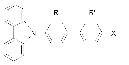
상기 식에서, R, R'은 각각 H이거나, 또는 탄소수 1 내지 22의 알킬기, 알콕시기, CN기, NO2기, 및 -O-Ar 중에서 선택될 수 있고, 상기 Ar은 페닐, 비페닐, 1-나프틸, 및 2-나프틸 중에서 선택될 수 있고, X는 O, CR2, NR, S, 또는 N=N이다.Wherein R and R 'are each H, or may be selected from an alkyl group having 1 to 22 carbon atoms, an alkoxy group, a CN group, a NO 2 group, and -O-Ar, wherein Ar is phenyl, biphenyl, 1 -Naphthyl, and 2-naphthyl, and X is O, CR 2 , NR, S, or N = N.

상기 식에서, R, R'은 각각 H이거나, 탄소수 1 내지 22의 알킬기, 알콕시기, CN기, NO2기, 및 -O-Ar 중에서 선택될 수 있고, 상기 Ar은 페닐, 비페닐, 1-나프틸, 및 2-나프틸 중에서 선택될 수 있고, X는 O, CR2, NR, S, 또는 N=N이다.Wherein R and R 'are each H, or an alkyl group having 1 to 22 carbon atoms, an alkoxy group, a CN group, a NO 2 group, and -O-Ar, wherein Ar is phenyl, biphenyl, 1- Naphthyl, and 2-naphthyl, and X is O, CR 2 , NR, S, or N = N.
상기 카바졸계 단위의 비제한적인 예로서는, 1,3,5-트리카바졸릴벤젠, 4,4'-비스카바졸릴비페닐(CBP), 폴리비닐카바졸, m-비스카바졸릴페닐, 4,4'-비스카바졸릴-2,2'-디메틸비페닐(dmCBP), 4,4',4"-트리(N-카바졸릴)트리페닐아민, 1,3,5-트리(2-카바졸릴페닐)벤젠, 1,3,5-트리스(2-카바졸릴-5-메톡시페닐)벤젠 및 비스(4-카 바졸릴페닐)실란으로 이루어진 군으로부터 선택된 하나 이상을 들 수 있다.Non-limiting examples of the carbazole-based unit include 1,3,5-tricarbazolylbenzene, 4,4'-biscarbazolylbiphenyl (CBP), polyvinylcarbazole, m-biscarbazolylphenyl, 4,4 '-Biscarbazolyl-2,2'-dimethylbiphenyl (dmCBP), 4,4', 4 "-tri (N-carbazolyl) triphenylamine, 1,3,5-tri (2-carbazolylphenyl ) Benzene, 1,3,5-tris (2-carbazolyl-5-methoxyphenyl) benzene and bis (4-carbazolylphenyl) silane.
상기 전자 수송 단위 B로 사용가능한 물질의 일예를 하기에 나타낸다.An example of the substance which can be used for the said electron transport unit B is shown below.

상기 식에서, R은 H이거나, 또는 탄소수 1 내지 22의 알킬기, 알콕시기, CN기, NO2기, 및 -O-Ar 중에서 선택될 수 있고, 상기 Ar은 페닐, 비페닐, 1-나프틸, 및 2-나프틸 중에서 선택될 수 있고, X는 O, CR2, NR, S, 또는 N=N이다.Wherein R is H or an alkyl group having 1 to 22 carbon atoms, an alkoxy group, a CN group, a NO 2 group, and -O-Ar, wherein Ar is phenyl, biphenyl, 1-naphthyl, And 2-naphthyl, X is O, CR 2 , NR, S, or N = N.
상기 플루오렌 단위의 비제한적인 예는 플루오렌(fluorene), 디메틸플루오렌(dimethylfluorene), 디페닐플루오렌(diphenylfluorene), 및 디에틸플루오렌(diethylfluorene) 등으로 이루어지는 군에서 선택된 하나 이상일 수 있다.Non-limiting examples of the fluorene unit may be at least one selected from the group consisting of fluorene, dimethylfluorene, diphenylfluorene, diethylfluorene and the like.
삭제delete
삭제delete
삭제delete

상기 식에서, R1, R2, R3, R4는 각각 H이거나, 또는 탄소수 1 내지 22개의 알킬기, 알콕시기, CN기, NO2기, 및 -O-Ar 중에서 선택될 수 있고, 상기 Ar은 페닐, 비페닐, 1-나프틸, 및 2-나프틸 중에서 선택될 수 있고, X는 O, CR2, NR, S, N=N이고, R은 R1과 같다.Wherein R1, R2, R3 and R4 are each H, or may be selected from an alkyl group having 1 to 22 carbon atoms, an alkoxy group, a CN group, a NO 2 group, and -O-Ar, wherein Ar is phenyl, a ratio Phenyl, 1-naphthyl, and 2-naphthyl, X is O, CR 2 , NR, S, N = N, and R is equal to R 1.
상기 스피로플루오렌 단위의 비제한적인 예는 페닐스피로플루오렌(phenylspirofluorene), 비페닐스피로플루오렌(biphenylspirofluorene), 및 메틸스피로플루오렌 (methylspirofluorene) 등으로 이루어진 군에서 선택된 하나 이상일 수 있다.Non-limiting examples of the spirofluorene unit may be at least one selected from the group consisting of phenylspirofluorene, biphenylspirofluorene, methylspirofluorene and the like.
상기 알루미늄 히드로퀴놀린(aluminum hydroquinoline) 단위는 하기의 화학식으로 표시된다.

삭제delete
삭제delete
삭제delete
삭제delete
본 발명의 일구현예에 의하면, 상기 단위 A 및 단위 B로 사용될 수 있는 물 질은 HOMO 에너지 전위와 LUMO 에너지 전위 중 적어도 하나는 서로 상이한 화합물인 것이 바람직하다. 즉, 단위 A의 HOMO 전위와 단위 B의 HOMO 전위가 동일하지 않거나, 또는 단위 A의 LUMO 전위와 단위 B의 LUMO 전위가 동일하지 않아야 한다.According to one embodiment of the invention, the material that can be used as the unit A and unit B is preferably at least one of the HOMO energy potential and LUMO energy potential is a different compound from each other. That is, the HOMO potential of the unit A and the HOMO potential of the unit B are not the same, or the LUMO potential of the unit A and the LUMO potential of the unit B must not be the same.
두 물질 단위의 에너지 레벨이 상이할 경우에는 홀과 전자가 주입되어 이동될 때보다 안정된 에너지 준위를 따라 이동하기 때문에 발광층에서 재결합(recombination) 확률이 높고 전하가 발광층 밖으로 유출되지 않는다. 두 물질의 에너지 레벨이 같으면 이러한 효과를 얻을 수 없다. 따라서 단위 A 및 단위 B가 될 수 있는 두 물질의 HOMO와 LUMO 에너지 준위 중 적어도 하나는 서로 상이하여야 안정된 에너지 준위를 따라 전하가 이동될 수 있다.When the energy levels of the two material units are different, since the holes and electrons move along a stable energy level than when injected and moved, the probability of recombination in the light emitting layer is high and charges do not flow out of the light emitting layer. If the two materials have the same energy level, this effect cannot be achieved. Therefore, at least one of the HOMO and LUMO energy levels of the two materials capable of being the unit A and the unit B must be different from each other so that charge can be transferred along the stable energy level.
또한 발광층의 인광 호스트 물질로 사용될 수 있는 바이폴라 물질은 상기 단위 A 및 단위 B가 각각의 삼중항 에너지 레벨(triplet energy level)이 2.0eV 이상인 것이 바람직하다. 상기 에너지 레벨이 2.0eV 미만인 경우에는 에너지 전이가 불완전하여 바람직하지 못하다.In addition, the bipolar material that can be used as the phosphorescent host material of the light emitting layer, it is preferable that the triplet energy level of each of the unit A and unit B is 2.0 eV or more. If the energy level is less than 2.0 eV, the energy transition is incomplete and undesirable.
상기 발광층에서 인광 호스트인 바이폴라 화합물의 함량은 발광층 형성재료 총중량(즉, 호스트와 도펀트의 총중량) 100 중량부를 기준으로 하여 70 내지 99 중량부인 것이 바람직하다. 만약 인광 호스트의 함량이 70 중량부 미만이면, 삼중항의 소광 현상이 일어나 효율이 저하되고, 99 중량부를 초과하면 발광 물질이 부족하여 효율 및 수명이 저하되어 바람직하지 못하다.The content of the bipolar compound that is the phosphorescent host in the light emitting layer is preferably 70 to 99 parts by weight based on 100 parts by weight of the total weight of the light emitting layer forming material (ie, the total weight of the host and the dopant). If the content of the phosphorescent host is less than 70 parts by weight, the quenching phenomenon of the triplet occurs and the efficiency is lowered. If the content of the phosphorescent host exceeds 99 parts by weight, the light emitting material is insufficient and the efficiency and lifespan are not preferable.
본 발명의 발광층 형성시 사용되는 인광 도펀트는 발광 물질로서, 이의 비제한적인 예로서, 비스티에닐피리딘 아세틸아세토네이트 이리듐(bisthienylpyridine acetylacetonate Iridium), 비스(벤조티에닐피리딘)아세틸아세토네이트 이리듐{bis(benzothienylpyridine)acetylacetonate Iridium}, 비스(2-페닐벤조티아졸)아세틸아세토네이트 이리듐{Bis(2-phenylbenzothiazole)acetylacetonate Iridium}, 비스(1-페닐이소퀴놀린) 이리듐 아세틸아세토네이트{bis(1-phenylisoquinoline) Iridium acetylacetonate}, 트리스(1-페닐이소퀴놀린)이리듐{tris(1-phenylisoquinoline) Iridium}, 트리스(페닐피리딘) 이리듐{tris(phenylpyridine) Iridium}, 트리스(2-비페닐피리딘) 이리듐{tris(2-phenylpyridine) Iridium}, 트리스(3-비페닐 피리딘) 이리듐{tris(3-biphenylpyridine) Iridium}, 또는 트리스(4-비페닐 피리딘) 이리듐{tris(4-biphenylpyridine) Iridium} 등을 들 수 있다.The phosphorescent dopant used in forming the light emitting layer of the present invention is a light emitting material, and non-limiting examples thereof include bisthienylpyridine acetylacetonate iridium, bis (benzothienylpyridine) acetylacetonate iridium {bis benzothienylpyridine) acetylacetonate Iridium}, bis (2-phenylbenzothiazole) acetylacetonate iridium {Bis (2-phenylbenzothiazole) acetylacetonate Iridium}, bis (1-phenylisoquinoline) iridium acetylacetonate {bis (1-phenylisoquinoline) Iridium acetylacetonate}, tris (1-phenylisoquinoline) iridium {tris (1-phenylisoquinoline) Iridium}, tris (phenylpyridine) Iridium}, tris (2-biphenylpyridine) iridium {tris (2- phenylpyridine) Iridium}, tris (3-biphenylpyridine) Iridium}, or tris (4-biphenylpyridine) Iridium {tris (4-biphenylpyridine) Iridium}. .
본 발명의 일구현예에 의하면, 상기 제1 전극과 상기 발광층 사이에 홀 주입층 및 홀 수송층 중에서 선택된 하나 이상이 더 구비할 수 있고, 상기 발광층과 제2 전극 사이에 홀 방지층, 전자수송층 및 전자주입층 중에서 선택된 하나 이상이 더 구비될 수 있다.According to an embodiment of the present invention, at least one selected from a hole injection layer and a hole transport layer may be further provided between the first electrode and the light emitting layer, and the hole blocking layer, the electron transport layer, and the electron may be provided between the light emitting layer and the second electrode. One or more selected from the injection layer may be further provided.
본 발명의 일구현예에 의하면, 발광층에서 인광 호스트로서 사용되는 바이폴라 화합물의 상기 단위 A는 4,4'-비스카바졸릴비페닐을 포함하고, 상기 단위 B는 알루미늄 히드로퀴놀린을 포함할 수 있다. 상기 바이폴라 화합물의 일예를 하기 화학식에 나타내었다:

삭제delete
상기 발광층의 인광 도펀트는 Ir(ppy)3이고, 이의 함량은 인광 호스트 100 중량부를 기준으로 하여 1 내지 30 중량부인 것이 바람직하다. 본 발명에 의한 바이폴라 화하물은 A 단위에 B 단위를 커플링하는 방법에 의하여 제조가능하다.The phosphorescent dopant of the light emitting layer is Ir (ppy) 3 , the content thereof is preferably 1 to 30 parts by weight based on 100 parts by weight of the phosphorescent host. The bipolar compound according to the present invention can be produced by a method of coupling a B unit to an A unit.
이하, 본 발명의 유기 전계 발광 소자의 제조방법을 살펴보면 다음과 같다.Hereinafter, the manufacturing method of the organic EL device of the present invention will be described.
도 1을 참조하여 본 발명의 일실시예에 따른 유기 전계 발광소자의 제조방법을 설명하면 다음과 같다.Referring to Figure 1 describes a method for manufacturing an organic EL device according to an embodiment of the present invention.
먼저 기판 상부에 제1전극인 애노드용 물질을 코팅하여 애노드를 형성한다. 여기에서 기판으로는 통상적인 유기 전계 발광 소자에서 사용되는 기판을 사용하는데 투명성, 표면 평활성, 취급용이성 및 방수성이 우수한 유기기판 또는 투명 플라스틱 기판이 바람직하다. 그리고 애노드용 물질로는 투명하고 전도성이 우수한 산화인듐주석(ITO), 산화인듐아연(IZO), 산화주석(SnO2), 산화아연(ZnO) 등을 사용한다.First, an anode is formed on a substrate by coating an anode material, which is a first electrode. Herein, a substrate used in a conventional organic electroluminescent device is used, and an organic substrate or a transparent plastic substrate having excellent transparency, surface smoothness, ease of handling, and waterproofness is preferable. As the anode material, indium tin oxide (ITO), indium zinc oxide (IZO), tin oxide (SnO 2 ), zinc oxide (ZnO), and the like, which are transparent and have excellent conductivity, are used.
상기 애노드 상부에 홀 주입층 물질을 진공 열증착, 또는 스핀 코팅하여 홀 주입층(HIL)을 선택적으로 형성한다. 여기에서 홀 주입층의 두께는 50 내지 1500Å인 것이 바람직하다. 만약 홀주입층의 두께가 50Å 미만인 경우에는 홀주입 특성이 저하되고, 1500Å을 초과하는 경우에는 구동전압 상승 때문에 바람직하지 못하다.A hole injection layer (HIL) is selectively formed by vacuum thermal evaporation or spin coating of the hole injection layer material on the anode. It is preferable that the thickness of a hole injection layer is 50-1500 kPa here. If the thickness of the hole injection layer is less than 50 kV, the hole injection characteristic is lowered, and if the thickness of the hole injection layer is more than 1500 kV, it is not preferable because of the increase of the driving voltage.
상기 홀 주입층 물질로는 특별히 제한되지 않으며 구리 프탈로시아닌(CuPc) 또는 스타버스트(Starburst)형 아민류인 TCTA, m-MTDATA, IDE406 (이데미쯔사 재료) 등을 홀 주입층으로 사용할 수 있다. The hole injection layer material is not particularly limited, and copper phthalocyanine (CuPc) or starburst type amines such as TCTA, m-MTDATA, IDE406 (Idemitsu Corp.), and the like may be used as the hole injection layer.

상기 과정에 따라 형성된 홀 주입층 상부에 홀 수송층 물질을 진공 열증착 또는 스핀 코팅하여 홀 수송층(HTL)을 선택적으로 형성한다. 상기 홀 수송층 물질은 특별히 제한되지는 않으며, N,N'-비스(3-메틸페닐)- N,N'-디페닐-[1,1-비페닐]-4,4'-디아민(TPD), N,N'-디(나프탈렌-1-일)-N,N'-디페닐 벤지딘,N,N'-디(나프탈렌-1-일) -N,N'-diphenyl- benxidine :α-NPD), IDE320(이데미쯔사 재료) 등이 사용된다. 여기에서 홀 수송층의 두께는 50 내지 1500Å인 것이 바람직하다. 만약 홀수송층의 두께가 50Å 미만인 경우에는 홀전달 특성이 저하되며 1500Å를 초과하는 경 우에는 구동전압 상승 때문에 바람직하지 못하다.A hole transport layer (HTL) is selectively formed by vacuum thermal evaporation or spin coating of the hole transport layer material on the hole injection layer formed by the above process. The hole transport layer material is not particularly limited, and N, N'-bis (3-methylphenyl) -N, N'-diphenyl- [1,1-biphenyl] -4,4'-diamine (TPD), N, N'-di (naphthalen-1-yl) -N, N'-diphenyl benzidine, N, N'-di (naphthalen-1-yl) -N, N'-diphenyl-benxidine: α-NPD) , IDE320 (Idemitsu Co., Ltd.), etc. are used. It is preferable that the thickness of a hole transport layer is 50-1500 kPa here. If the thickness of the hole transport layer is less than 50 kV, the hole transport property is deteriorated.

이어서 홀 수송층 상부에, 인광 호스트로서 상술한 바이폴라 화합물과, 인광 도펀트를 함께 사용하여 발광층(EML)이 형성된다. 여기에서 발광층 형성 방법은 특별하게 제한되지는 않으나, 진공 증착, 잉크젯 프린팅, 레이저 전사법, 포토리소그래피법(photolithography)등의 방법을 이용한다.Subsequently, the light emitting layer EML is formed on the hole transport layer by using the above-described bipolar compound as a phosphorescent host and a phosphorescent dopant together. The light emitting layer forming method is not particularly limited, but a method such as vacuum deposition, inkjet printing, laser transfer, photolithography, or the like is used.
상기 발광층의 두께는 100 내지 800 Å인 것이 바람직하고, 300 내지 400 Å인것이 더욱 바람직하다. 만약 발광층의 두께가 100Å 미만이면, 효율 및 수명이 저하되고, 800 Å을 초과하면 구동전압이 상승하여 바람직하지 못하다.It is preferable that it is 100-800 GPa, and, as for the thickness of the said light emitting layer, it is more preferable that it is 300-400 GPa. If the thickness of the light emitting layer is less than 100 kW, the efficiency and lifetime are lowered. If the thickness of the light emitting layer is more than 800 kW, the driving voltage increases, which is not preferable.
상기 발광층 위에 홀 블로킹용 물질을 진공 증착 또는 스핀코팅하여 홀 블로킹층(HBL)을 선택적으로 형성된다. 이 때 사용되는 홀 블로킹층용 물질은 특별히 제한되지는 않으나 전자 수송 능력을 가지면서 발광 화합물 보다 높은 이온화 퍼텐셜을 가져야 하며 대표적으로 Balq, BCP, TPBI 등이 사용된다. 만약 홀블로킹층의 두께는 30 내지 500Å인 것이 바람직하다. 만약 홀블로킹층의 두께가 30 Å 미만인 경우에는 정공 방지 특성이 좋지 않아 효율이 저하되며, 500Å를 초과하는 경우에 는 구동전압 상승으로 바람직하지 못하다.The hole blocking layer HBL is selectively formed on the light emitting layer by vacuum deposition or spin coating a material for hole blocking. The material for the hole blocking layer used at this time is not particularly limited, but should have ionization potential higher than that of the light emitting compound while having electron transport ability, and typically, Balq, BCP, TPBI, and the like are used. If the thickness of the hole blocking layer is preferably 30 to 500 kPa. If the thickness of the hole blocking layer is less than 30 kW, the hole blocking property is not good, and thus the efficiency is lowered.

상기 홀 블로킹층 위에 전자 수송층이 진공 증착 방법, 또는 스핀 코팅 방법으로서 전자수송층(ETL)을 형성한다. 전자 수송층 재료로서는 특별히 제한되지는 않으며 Alq3를 이용할 수 있다. 상기 전자수송층의 두께는 50 내지 600Å인 것이 바람직하다. 만약 전자수송층의 두께가 50Å 미만인 경우에는 수명 특성이 저하되며, 600Å를 초과하는 경우에는 구동전압 상승으로 바람직하지 못하다.An electron transport layer forms an electron transport layer (ETL) on the hole blocking layer as a vacuum deposition method or a spin coating method. It does not restrict | limit especially as an electron carrying layer material, Alq3 can be used. It is preferable that the thickness of the said electron carrying layer is 50-600 GPa. If the thickness of the electron transport layer is less than 50 kW, the lifespan characteristics are lowered. If the electron transport layer is more than 600 kW, it is not preferable to increase the driving voltage.
또한 상기 전자 수송층 위에 전자 주입층(EIL)이 선택적으로 적층될 수 있다. 상기 전자 주입층 형성 재료로서는 LiF, NaCl, CsF, Li2O, BaO, Liq 등의 물질을 이용할 수 있다. 상기 전자 주입층의 두께는 1 내지 100Å인 것이 바람직하다. 만약 전자주입층의 두께가 1Å 미만인 경우에는 효과적인 전자주입층으로서 역할을 못하여 구동전압이 높고, 100Å를 초과하는 경우에는 절연층으로 작용하여 구동전 압이 높아 바람직하지 못하다.In addition, an electron injection layer EIL may be selectively stacked on the electron transport layer. As the electron injection layer forming material, materials such as LiF, NaCl, CsF, Li 2 O, BaO, and Liq can be used. It is preferable that the thickness of the said electron injection layer is 1-100 kPa. If the thickness of the electron injection layer is less than 1 kW, the driving voltage is not high because it does not serve as an effective electron injection layer, and if it exceeds 100 kW, the driving voltage acts as an insulating layer.

이어서, 상기 전자주입층 상부에 제2전극인 캐소드용 금속을 진공열 증착하여 제2전극인 캐소드를 형성함으로써 유기 전계 발광 소자가 완성된다.Subsequently, the organic electroluminescent device is completed by forming a cathode, which is a second electrode, by vacuum-heat deposition of a cathode metal, which is a second electrode, on the electron injection layer.
상기 캐소드 금속으로는 리튬(Li), 마그네슘(Mg), 알루미늄(Al), 알루미늄-리튬(Al-Li), 칼슘(Ca), 마그네슘-인듐(Mg-In), 마그네슘-은(Mg-Ag) 등이 이용된다. The cathode metal is lithium (Li), magnesium (Mg), aluminum (Al), aluminum-lithium (Al-Li), calcium (Ca), magnesium-indium (Mg-In), magnesium-silver (Mg-Ag ) And the like are used.
본 발명의 유기 전계 발광 소자는 애노드, 홀 주입층, 홀 수송층, 발광층, 전자 수송층, 전자 주입층, 캐소드의 필요에 따라 한 층 또는 두 층의 중간층을 더 형성하는 것도 가능하다. 위에서 언급한 층 외에도 홀 블록킹층, 전자 블로킹층이 들어갈 수도 있다.The organic electroluminescent device of the present invention may further form an intermediate layer of one or two layers according to the needs of the anode, the hole injection layer, the hole transport layer, the light emitting layer, the electron transport layer, the electron injection layer, and the cathode. In addition to the above-mentioned layers, a hole blocking layer and an electron blocking layer may also be included.
이하, 본 발명을 하기 실시예를 들어 설명하기로 하되, 본 발명이 하기 실시예로만 한정되는 것은 아니다.Hereinafter, the present invention will be described with reference to the following examples, but the present invention is not limited only to the following examples.
바이폴라 물질의 제조Preparation of Bipolar Material
2-methyl-8-quinolinol(0.01 mole)을 에탄올과 물의 혼합용액에서 재결정한후 재결정한 물질을 aluminum isopropoxide(0.005 mole)와 무수 diethylether에서 교반한다. 30분 반응후 용액을 필터한 후 hydroxycarbazolebiphenyl(0.01 mole)을 diethylether 용액에 넣어 가열하여 6시간 동안 반응시킨 후 냉각한다. 고체물질을 얻은 후 washing하고 drying하여 본 화합물을 제조한다.After 2-methyl-8-quinolinol (0.01 mole) is recrystallized from a mixture of ethanol and water, the recrystallized material is stirred in aluminum isopropoxide (0.005 mole) and anhydrous diethylether. After 30 minutes, the solution was filtered and hydroxycarbazolebiphenyl (0.01 mole) was added to a diethylether solution, heated for 6 hours, and then cooled. After obtaining a solid material, the compound is prepared by washing and drying.
실시예 1Example 1
애노드는 코닝(corning) 15Ω/cm2 (1200Å) ITO 유리 기판을 50mm x 50mm x 0.7mm 크기로 잘라서 이소프로필 알코올과 순수 물 속에서 각 5 분 동안 초음파 세정한 후, 30분 동안 UV, 오존 세정하여 사용하였다.The anode cuts a corning 15Ω / cm 2 (1200Å) ITO glass substrate to 50mm x 50mm x 0.7mm and ultrasonically cleans for 5 minutes in isopropyl alcohol and pure water, followed by UV and ozone cleaning for 30 minutes. Was used.
상기 기판 상부에 N,N'-디(1-나프틸)-N,N'-디페닐벤지딘(NPD)을 진공 증착하여 홀 수송층을 600Å 두께로 형성하였다.N, N'-di (1-naphthyl) -N, N'-diphenylbenzidine (NPD) was vacuum deposited on the substrate to form a hole transport layer having a thickness of 600 kPa.
상기 홀 수송층 상부에 인광 호스트로서 상기 제조한 바이폴라 화합물 90 중량부와 인광 도펀트인 트리스(2-페닐피리딘)이리듐(tris(2-phenylpyridine) Iridium) 10 중량부를 진공증착하여 약 400Å의 두께로 발광층을 형성하였다.90 parts by weight of the bipolar compound prepared above as the phosphorescent host and 10 parts by weight of the phosphorescent dopant tris (2-phenylpyridine) iridium were vacuum deposited on the hole transport layer to form a light emitting layer having a thickness of about 400 kPa. Formed.
상기 발광층 상부에 전자 수송 물질인 Alq3를 증착하여 약 300Å 두께의 전자 수송층을 형성하였다.Alq3, an electron transporting material, was deposited on the emission layer to form an electron transporting layer having a thickness of about 300 kHz.
상기 전자 수송층 상부에 LiF 10Å (전자 주입층)과 Al 1000Å (캐소드)을 순차적으로 진공 증착하여 LiF/Al 전극을 형성하여 도 1에 도시한 바와 같은 유기 전계 발광 소자를 제조하였다.LiF 10 전극 (electron injection layer) and Al 1000 Å (cathode) were sequentially vacuum deposited on the electron transport layer to form a LiF / Al electrode, thereby manufacturing an organic EL device as shown in FIG. 1.
비교예 1Comparative Example 1
애노드는 코닝(corning) 15Ω/cm2 (1200Å) ITO 유리 기판을 50mm x 50mm x 0.7mm 크기로 잘라서 이소프로필 알코올과 순수 물 속에서 각 5 분 동안 초음파 세정한 후, 30분 동안 UV, 오존 세정하여 사용하였다.The anode cut a Corning 15Ω / cm 2 (1200Å) ITO glass substrate into 50mm x 50mm x 0.7mm, ultrasonically cleaned in isopropyl alcohol and pure water for 5 minutes, and then UV and ozone cleaned for 30 minutes. Was used.
상기 기판 상부에 NPD를 진공 증착하여 홀 수송층을 600Å 두께로 형성하였다. 상기 홀 수송층 상부에 인광 호스트인 4,4'-비스카바졸릴비페닐에 인광 도펀트인 트리스(2-페닐피리딘)이리듐(tris(2-phenylpyridine) Iridium) 10 중량부를 진공증착하여 약 400Å의 두께로 발광층을 형성하였다.NPD was vacuum deposited on the substrate to form a hole transport layer having a thickness of 600 mm3. 10 parts by weight of phosphorus dopant tris (2-phenylpyridine) iridium (phosphorescent dopant) was deposited on 4,4'-biscarbazolyl biphenyl as a phosphorescent host on the hole transport layer to a thickness of about 400 kPa. A light emitting layer was formed.
상기 발광층 상부에 전자 수송 물질인 Alq3를 증착하여 약 300Å 두께의 전자 수송층을 형성하였다.Alq3, an electron transporting material, was deposited on the emission layer to form an electron transporting layer having a thickness of about 300 kHz.
상기 전자 수송층 상부에 LiF 10Å (전자 주입층)과 Al 1000Å (캐소드)을 순차적으로 진공 증착하여 LiF/Al 전극을 형성하여 도 1에 도시한 바와 같은 유기 전계 발광 소자를 제조하였다.LiF 10 전극 (electron injection layer) and Al 1000 Å (cathode) were sequentially vacuum deposited on the electron transport layer to form a LiF / Al electrode, thereby manufacturing an organic EL device as shown in FIG. 1.
상기 실시예 1 및 비교예 1에 따라 제조된 유기 전계 발광 소자에 있어서, 효율 및 수명 특성을 조사하였다.In the organic EL device manufactured according to Example 1 and Comparative Example 1, the efficiency and lifespan characteristics were investigated.
그 결과, 비교예 1의 유기 전계 발광 소자의 효율은 약 24cd/A이고, 실시예 1의 유기 전계 발광 소자는 효율이 31cd/A로서, 비교예 1의 경우에 비하여 효율이 개선되었다.As a result, the efficiency of the organic EL device of Comparative Example 1 was about 24 cd / A, and the efficiency of the organic electroluminescent device of Example 1 was 31 cd / A, which was improved compared to that of Comparative Example 1.
또한, 수명 특성은 최초 발광 휘도가 50%선까지 감소하는 시간으로 나타내는데 실시예 1의 유기 전계 발광 소자는 1000cd/m2에서 7,000시간이고, 비교예 1의 유기 전계 발광 소자는 1000cd/m2에서 5,000시간으로 나타나 실시예 1은 비교예 1의 경우에 비하여 수명 특성이 개선됨을 확인할 수 있었다.In addition, the lifespan characteristics are represented by the time when the initial emission luminance decreases by 50%. The organic electroluminescent device of Example 1 is 7,000 hours at 1000 cd / m 2 , and the organic electroluminescent device of Comparative Example 1 is 1000 cd / m 2 . As shown in 5,000 hours, Example 1 was confirmed to improve the life characteristics compared to the case of Comparative Example 1.
본 발명의 유기 전계 발광 소자는 발광층 형성시 홀 수송 단위와 전자 수송 단위를 함께 갖는 바이폴라 화합물을 인광 디바이스의 인광 호스트로 사용함으로써 정공 수송성 물질 및 전자 수송성 물질을 혼합한 효과와 유사한 효과를 얻을 수 있다. 또한 단일 물질을 사용하여 두 물질을 혼합한 효과를 얻을 수 있으며 디바이스의 효율 및 수명 특성을 개선할 수 있다. The organic electroluminescent device of the present invention can obtain an effect similar to the effect of mixing a hole transporting material and an electron transporting material by using a bipolar compound having both a hole transporting unit and an electron transporting unit as a phosphorescent host in forming a light emitting layer. . In addition, a single material can be used to achieve the effect of mixing the two materials and improve the efficiency and lifetime characteristics of the device.
Claims (17)


Priority Applications (4)
| Application Number | Priority Date | Filing Date | Title |
|---|---|---|---|
| KR1020040089652A KR100787423B1 (en) | 2004-11-05 | 2004-11-05 | Organic electroluminescent element |
| JP2005306313A JP4571057B2 (en) | 2004-11-05 | 2005-10-20 | Organic electroluminescence device |
| CNA2005101154883A CN1772839A (en) | 2004-11-05 | 2005-11-04 | Organic illuminating device |
| US11/266,248 US7651790B2 (en) | 2004-11-05 | 2005-11-04 | Organic light-emitting device |
Applications Claiming Priority (1)
| Application Number | Priority Date | Filing Date | Title |
|---|---|---|---|
| KR1020040089652A KR100787423B1 (en) | 2004-11-05 | 2004-11-05 | Organic electroluminescent element |
Publications (2)
| Publication Number | Publication Date |
|---|---|
| KR20060040830A KR20060040830A (en) | 2006-05-11 |
| KR100787423B1 true KR100787423B1 (en) | 2007-12-26 |
Family
ID=36728536
Family Applications (1)
| Application Number | Title | Priority Date | Filing Date |
|---|---|---|---|
| KR1020040089652A Expired - Lifetime KR100787423B1 (en) | 2004-11-05 | 2004-11-05 | Organic electroluminescent element |
Country Status (4)
| Country | Link |
|---|---|
| US (1) | US7651790B2 (en) |
| JP (1) | JP4571057B2 (en) |
| KR (1) | KR100787423B1 (en) |
| CN (1) | CN1772839A (en) |
Families Citing this family (24)
| Publication number | Priority date | Publication date | Assignee | Title |
|---|---|---|---|---|
| KR101272435B1 (en) * | 2004-12-30 | 2013-06-07 | 이 아이 듀폰 디 네모아 앤드 캄파니 | Organometallic complexes |
| KR100787428B1 (en) | 2005-03-05 | 2007-12-26 | 삼성에스디아이 주식회사 | Organic electroluminescent element |
| KR100732823B1 (en) * | 2005-04-21 | 2007-06-27 | 삼성에스디아이 주식회사 | Organometallic compound in which a host compound and a dopant compound are connected, an organic electroluminescent device using the same, and a manufacturing method thereof |
| TWI297353B (en) * | 2005-11-10 | 2008-06-01 | Au Optronics Corp | Phosphorescent organic light-emitting diodes |
| CN101931056B (en) * | 2006-06-01 | 2014-07-09 | 株式会社半导体能源研究所 | Light-emitting element, light-emitting device and an electronic device |
| GB0617167D0 (en) * | 2006-08-31 | 2006-10-11 | Cdt Oxford Ltd | Compounds for use in opto-electrical devices |
| US9397308B2 (en) * | 2006-12-04 | 2016-07-19 | Semiconductor Energy Laboratory Co., Ltd. | Light emitting element, light emitting device, and electronic device |
| US8617720B2 (en) | 2009-12-21 | 2013-12-31 | E I Du Pont De Nemours And Company | Electroactive composition and electronic device made with the composition |
| TWI432418B (en) * | 2011-12-19 | 2014-04-01 | Au Optronics Corp | Electron transport material and organic light emitting device |
| JP6317544B2 (en) | 2013-02-15 | 2018-04-25 | 出光興産株式会社 | Organic electroluminescence device and electronic device |
| CN104177287A (en) * | 2013-05-28 | 2014-12-03 | 海洋王照明科技股份有限公司 | Red light phosphorescent host material, preparation method and organic electroluminescent device thereof |
| WO2015099481A1 (en) * | 2013-12-27 | 2015-07-02 | 주식회사 두산 | Organic electroluminescent device |
| KR101742359B1 (en) | 2013-12-27 | 2017-05-31 | 주식회사 두산 | Organic electro luminescence device |
| EP3051604B1 (en) | 2015-01-30 | 2017-10-11 | Samsung Display Co., Ltd. | Organic light-emitting device |
| JP2018525331A (en) | 2015-06-10 | 2018-09-06 | メルク パテント ゲーエムベーハー | Materials for organic electroluminescent devices |
| CN107922359A (en) | 2015-07-30 | 2018-04-17 | 默克专利有限公司 | Material for organic electroluminescence device |
| KR102537438B1 (en) | 2015-11-24 | 2023-05-30 | 삼성디스플레이 주식회사 | Compound and Organic light emitting device comprising same |
| KR102552273B1 (en) | 2015-11-26 | 2023-07-07 | 삼성디스플레이 주식회사 | Condensed cyclic compound and organic light emitting device comprising the same |
| KR102546673B1 (en) * | 2015-12-03 | 2023-06-23 | 삼성디스플레이 주식회사 | Organic light emitting device and display device having the same |
| KR102642199B1 (en) | 2016-04-07 | 2024-03-05 | 삼성디스플레이 주식회사 | Organic light emitting device |
| JP7039188B2 (en) * | 2016-06-24 | 2022-03-22 | 株式会社半導体エネルギー研究所 | Host material for phosphorescent layer, organic compound, light emitting element, light emitting device, electronic device and lighting device |
| CN108129661B (en) * | 2018-01-03 | 2021-01-22 | 京东方科技集团股份有限公司 | Polymer, quantum dot film layer and preparation method thereof |
| CN109994640B (en) * | 2019-04-09 | 2021-06-15 | 江苏三月科技股份有限公司 | Organic electroluminescent device containing multi-channel carrier transmission material |
| KR102827754B1 (en) * | 2021-02-10 | 2025-07-03 | 삼성디스플레이 주식회사 | Light-emitting device and electronic apparatus including the same |
Citations (2)
| Publication number | Priority date | Publication date | Assignee | Title |
|---|---|---|---|---|
| EP1065737A2 (en) | 1999-06-28 | 2001-01-03 | Motorola, Inc. | Organic electroluminescent device |
| JP2002226722A (en) * | 2001-01-30 | 2002-08-14 | Sony Corp | Aminostyrylphenanthrene compounds, synthetic intermediates thereof, and methods for producing them |
Family Cites Families (16)
| Publication number | Priority date | Publication date | Assignee | Title |
|---|---|---|---|---|
| US5141671A (en) * | 1991-08-01 | 1992-08-25 | Eastman Kodak Company | Mixed ligand 8-quinolinolato aluminum chelate luminophors |
| US6242115B1 (en) * | 1997-09-08 | 2001-06-05 | The University Of Southern California | OLEDs containing thermally stable asymmetric charge carrier materials |
| EP1394870B2 (en) * | 1997-10-09 | 2018-10-17 | The Trustees Of Princeton University | Phosphorescent organic light emitting device |
| US6451455B1 (en) * | 1998-04-01 | 2002-09-17 | The Trustees Of Princeton University | Metal complexes bearing both electron transporting and hole transporting moieties |
| KR100582328B1 (en) * | 1998-04-09 | 2006-05-23 | 이데미쓰 고산 가부시키가이샤 | Organic electroluminescent device |
| KR100946314B1 (en) * | 1999-12-01 | 2010-03-09 | 더 트러스티즈 오브 프린스턴 유니버시티 | Organic light emitting device comprising a phosphorescent organo metallic compound |
| US6225467B1 (en) * | 2000-01-21 | 2001-05-01 | Xerox Corporation | Electroluminescent (EL) devices |
| JP4089331B2 (en) * | 2001-07-25 | 2008-05-28 | 東レ株式会社 | Light emitting element |
| JP2003229277A (en) * | 2002-02-04 | 2003-08-15 | Matsushita Electric Ind Co Ltd | Light emitting device material, light emitting device and device using the same |
| EP1489155A4 (en) * | 2002-03-22 | 2006-02-01 | Idemitsu Kosan Co | MATERIAL FOR ORGANIC ELECTROLUMINESCENT DEVICES AND ORGANIC ELECTROLUMINESCENT DEVICES PRODUCED WITH THIS MATERIAL |
| US6902831B2 (en) * | 2002-11-26 | 2005-06-07 | Canon Kabushiki Kaisha | Azulene-based compounds in organic light emitting device elements |
| JP4225043B2 (en) * | 2002-12-03 | 2009-02-18 | コニカミノルタホールディングス株式会社 | ORGANIC ELECTROLUMINESCENT DEVICE, ITS MANUFACTURING METHOD, DISPLAY DEVICE, LIGHTING DEVICE, AND LIGHT SOURCE |
| JP4580342B2 (en) * | 2003-01-24 | 2010-11-10 | 出光興産株式会社 | Organic electroluminescence device |
| CN100335462C (en) * | 2003-09-05 | 2007-09-05 | 清华大学 | Carbazole derivative and its application in electroluminescent device |
| JP4576141B2 (en) * | 2004-03-26 | 2010-11-04 | 保土谷化学工業株式会社 | Carbazole derivatives containing fluorene groups |
| KR101272435B1 (en) * | 2004-12-30 | 2013-06-07 | 이 아이 듀폰 디 네모아 앤드 캄파니 | Organometallic complexes |
-
2004
- 2004-11-05 KR KR1020040089652A patent/KR100787423B1/en not_active Expired - Lifetime
-
2005
- 2005-10-20 JP JP2005306313A patent/JP4571057B2/en not_active Expired - Lifetime
- 2005-11-04 US US11/266,248 patent/US7651790B2/en active Active
- 2005-11-04 CN CNA2005101154883A patent/CN1772839A/en active Pending
Patent Citations (2)
| Publication number | Priority date | Publication date | Assignee | Title |
|---|---|---|---|---|
| EP1065737A2 (en) | 1999-06-28 | 2001-01-03 | Motorola, Inc. | Organic electroluminescent device |
| JP2002226722A (en) * | 2001-01-30 | 2002-08-14 | Sony Corp | Aminostyrylphenanthrene compounds, synthetic intermediates thereof, and methods for producing them |
Also Published As
| Publication number | Publication date |
|---|---|
| CN1772839A (en) | 2006-05-17 |
| US20060263631A1 (en) | 2006-11-23 |
| JP4571057B2 (en) | 2010-10-27 |
| JP2006135315A (en) | 2006-05-25 |
| KR20060040830A (en) | 2006-05-11 |
| US7651790B2 (en) | 2010-01-26 |
Similar Documents
| Publication | Publication Date | Title |
|---|---|---|
| KR100787423B1 (en) | Organic electroluminescent element | |
| KR100708655B1 (en) | Organic electroluminescent element | |
| KR100751316B1 (en) | Organic electroluminescent element | |
| JP4362461B2 (en) | Organic electroluminescence device | |
| KR100787428B1 (en) | Organic electroluminescent element | |
| KR100696505B1 (en) | Organic electroluminescent device and manufacturing method thereof | |
| KR100669775B1 (en) | Organic electroluminescent element | |
| KR20060040829A (en) | Organic electroluminescent element | |
| KR100669790B1 (en) | Organic electroluminescent element | |
| KR100696470B1 (en) | Organic electroluminescent element | |
| KR100603404B1 (en) | Organic electroluminescent element | |
| KR100669776B1 (en) | Organic electroluminescent element | |
| KR100581918B1 (en) | Organic electroluminescent element | |
| KR100669777B1 (en) | Organic electroluminescence display | |
| KR100659072B1 (en) | Organic electroluminescent element |
Legal Events
| Date | Code | Title | Description |
|---|---|---|---|
| A201 | Request for examination | ||
| PA0109 | Patent application |
Patent event code: PA01091R01D Comment text: Patent Application Patent event date: 20041105 |
|
| PA0201 | Request for examination | ||
| PG1501 | Laying open of application | ||
| E902 | Notification of reason for refusal | ||
| PE0902 | Notice of grounds for rejection |
Comment text: Notification of reason for refusal Patent event date: 20060529 Patent event code: PE09021S01D |
|
| E90F | Notification of reason for final refusal | ||
| PE0902 | Notice of grounds for rejection |
Comment text: Final Notice of Reason for Refusal Patent event date: 20061128 Patent event code: PE09021S02D |
|
| E902 | Notification of reason for refusal | ||
| PE0902 | Notice of grounds for rejection |
Comment text: Notification of reason for refusal Patent event date: 20070530 Patent event code: PE09021S01D |
|
| E701 | Decision to grant or registration of patent right | ||
| PE0701 | Decision of registration |
Patent event code: PE07011S01D Comment text: Decision to Grant Registration Patent event date: 20071127 |
|
| GRNT | Written decision to grant | ||
| PR0701 | Registration of establishment |
Comment text: Registration of Establishment Patent event date: 20071213 Patent event code: PR07011E01D |
|
| PR1002 | Payment of registration fee |
Payment date: 20071214 End annual number: 3 Start annual number: 1 |
|
| PG1601 | Publication of registration | ||
| PR1001 | Payment of annual fee |
Payment date: 20101129 Start annual number: 4 End annual number: 4 |
|
| PR1001 | Payment of annual fee |
Payment date: 20111129 Start annual number: 5 End annual number: 5 |
|
| FPAY | Annual fee payment |
Payment date: 20121130 Year of fee payment: 6 |
|
| PR1001 | Payment of annual fee |
Payment date: 20121130 Start annual number: 6 End annual number: 6 |
|
| FPAY | Annual fee payment |
Payment date: 20131129 Year of fee payment: 7 |
|
| PR1001 | Payment of annual fee |
Payment date: 20131129 Start annual number: 7 End annual number: 7 |
|
| FPAY | Annual fee payment |
Payment date: 20141128 Year of fee payment: 8 |
|
| PR1001 | Payment of annual fee |
Payment date: 20141128 Start annual number: 8 End annual number: 8 |
|
| FPAY | Annual fee payment |
Payment date: 20181126 Year of fee payment: 12 |
|
| PR1001 | Payment of annual fee |
Payment date: 20181126 Start annual number: 12 End annual number: 12 |
|
| FPAY | Annual fee payment |
Payment date: 20191202 Year of fee payment: 13 |
|
| PR1001 | Payment of annual fee |
Payment date: 20191202 Start annual number: 13 End annual number: 13 |
|
| PR1001 | Payment of annual fee |
Payment date: 20201201 Start annual number: 14 End annual number: 14 |
|
| PR1001 | Payment of annual fee |
Payment date: 20211125 Start annual number: 15 End annual number: 15 |
|
| PC1801 | Expiration of term |
Termination date: 20250505 Termination category: Expiration of duration |