KR100659072B1 - Organic electroluminescent element - Google Patents
Organic electroluminescent element Download PDFInfo
- Publication number
- KR100659072B1 KR100659072B1 KR1020040094912A KR20040094912A KR100659072B1 KR 100659072 B1 KR100659072 B1 KR 100659072B1 KR 1020040094912 A KR1020040094912 A KR 1020040094912A KR 20040094912 A KR20040094912 A KR 20040094912A KR 100659072 B1 KR100659072 B1 KR 100659072B1
- Authority
- KR
- South Korea
- Prior art keywords
- light emitting
- bis
- organic electroluminescent
- iridium
- electroluminescent device
- Prior art date
- Legal status (The legal status is an assumption and is not a legal conclusion. Google has not performed a legal analysis and makes no representation as to the accuracy of the status listed.)
- Expired - Lifetime
Links
Images


Classifications
-
- C—CHEMISTRY; METALLURGY
- C09—DYES; PAINTS; POLISHES; NATURAL RESINS; ADHESIVES; COMPOSITIONS NOT OTHERWISE PROVIDED FOR; APPLICATIONS OF MATERIALS NOT OTHERWISE PROVIDED FOR
- C09K—MATERIALS FOR MISCELLANEOUS APPLICATIONS, NOT PROVIDED FOR ELSEWHERE
- C09K11/00—Luminescent, e.g. electroluminescent, chemiluminescent materials
- C09K11/06—Luminescent, e.g. electroluminescent, chemiluminescent materials containing organic luminescent materials
-
- H—ELECTRICITY
- H10—SEMICONDUCTOR DEVICES; ELECTRIC SOLID-STATE DEVICES NOT OTHERWISE PROVIDED FOR
- H10K—ORGANIC ELECTRIC SOLID-STATE DEVICES
- H10K50/00—Organic light-emitting devices
- H10K50/10—OLEDs or polymer light-emitting diodes [PLED]
- H10K50/11—OLEDs or polymer light-emitting diodes [PLED] characterised by the electroluminescent [EL] layers
-
- H—ELECTRICITY
- H10—SEMICONDUCTOR DEVICES; ELECTRIC SOLID-STATE DEVICES NOT OTHERWISE PROVIDED FOR
- H10K—ORGANIC ELECTRIC SOLID-STATE DEVICES
- H10K50/00—Organic light-emitting devices
- H10K50/10—OLEDs or polymer light-emitting diodes [PLED]
- H10K50/14—Carrier transporting layers
- H10K50/15—Hole transporting layers
-
- H—ELECTRICITY
- H10—SEMICONDUCTOR DEVICES; ELECTRIC SOLID-STATE DEVICES NOT OTHERWISE PROVIDED FOR
- H10K—ORGANIC ELECTRIC SOLID-STATE DEVICES
- H10K50/00—Organic light-emitting devices
- H10K50/10—OLEDs or polymer light-emitting diodes [PLED]
- H10K50/14—Carrier transporting layers
- H10K50/16—Electron transporting layers
-
- H—ELECTRICITY
- H10—SEMICONDUCTOR DEVICES; ELECTRIC SOLID-STATE DEVICES NOT OTHERWISE PROVIDED FOR
- H10K—ORGANIC ELECTRIC SOLID-STATE DEVICES
- H10K50/00—Organic light-emitting devices
- H10K50/10—OLEDs or polymer light-emitting diodes [PLED]
- H10K50/17—Carrier injection layers
-
- H—ELECTRICITY
- H10—SEMICONDUCTOR DEVICES; ELECTRIC SOLID-STATE DEVICES NOT OTHERWISE PROVIDED FOR
- H10K—ORGANIC ELECTRIC SOLID-STATE DEVICES
- H10K50/00—Organic light-emitting devices
- H10K50/10—OLEDs or polymer light-emitting diodes [PLED]
- H10K50/17—Carrier injection layers
- H10K50/171—Electron injection layers
-
- Y—GENERAL TAGGING OF NEW TECHNOLOGICAL DEVELOPMENTS; GENERAL TAGGING OF CROSS-SECTIONAL TECHNOLOGIES SPANNING OVER SEVERAL SECTIONS OF THE IPC; TECHNICAL SUBJECTS COVERED BY FORMER USPC CROSS-REFERENCE ART COLLECTIONS [XRACs] AND DIGESTS
- Y10—TECHNICAL SUBJECTS COVERED BY FORMER USPC
- Y10S—TECHNICAL SUBJECTS COVERED BY FORMER USPC CROSS-REFERENCE ART COLLECTIONS [XRACs] AND DIGESTS
- Y10S428/00—Stock material or miscellaneous articles
- Y10S428/917—Electroluminescent
Landscapes
- Physics & Mathematics (AREA)
- Optics & Photonics (AREA)
- Chemical & Material Sciences (AREA)
- Engineering & Computer Science (AREA)
- Materials Engineering (AREA)
- Organic Chemistry (AREA)
- Electroluminescent Light Sources (AREA)
Abstract
본 발명은 한 쌍의 전극 사이에 발광층을 갖는 유기 전계 발광 소자에 있어서, 상기 발광층은 둘 이상의 발광 호스트 물질, 도펀트 및 발광보조제(sensitizer)를 포함하는 것을 특징으로 하는 유기 전계 발광 소자를 제공한다. 본 발명에 따른 발광 보조제를 이용하면 에너지 전달 효율을 증가시켜 디바이스의 효율 및 수명 특성을 개선할 수 있다.The present invention provides an organic electroluminescent device having a light emitting layer between a pair of electrodes, wherein the light emitting layer includes at least two light emitting host materials, a dopant and a light emitting assistant. By using the light emission aid according to the present invention it is possible to increase the energy transfer efficiency to improve the efficiency and life characteristics of the device.
Description
도 1은 본 발명의 일실시예에 따른 유기 전계 발광 소자의 단면을 나타낸 도면이다.1 is a cross-sectional view of an organic electroluminescent device according to an embodiment of the present invention.
도 2는 유기 전계 발광 소자의 효율 특성에 대한 본 발명에 의한 일실시예 및 비교예를 나타낸 도면이다.2 is a view showing an embodiment and a comparative example according to the present invention for the efficiency characteristics of the organic electroluminescent device.
도 3은 유기 전계 발광 소자의 수명 특성에 대한 본 발명에 의한 일실시예 및 비교예를 나타낸 도면이다.3 is a view showing an embodiment and a comparative example according to the present invention for the life characteristics of the organic EL device.
본 발명은 유기 전계 발광 소자에 관한 것으로서, 보다 상세하기로는 발광 보조제를 사용함으로써 효율 및 수명 특성이 개선된 유기 전계 발광 소자에 관한 것이다.The present invention relates to an organic electroluminescent device, and more particularly, to an organic electroluminescent device having improved efficiency and lifespan characteristics by using a light emission aid.
전계 발광 소자(Electroluminescent device : EL device)는 자발광형 표시소자로서 시야각이 넓고 콘트라스트가 우수할 뿐만 아니라 응답시간이 빠르다는 장점을 가지고 있다. EL 소자는 발광층(emitting layer) 형성용 재료에 따라 무기 EL 소자와 유기 EL 소자로 구분된다. 여기에서 유기 EL 소자는 무기 EL소자에 비하여 휘도, 구동전압 및 응답속도 특성이 우수하고 다색화가 가능하다는 장점을 가지고 있다.Electroluminescent devices (EL devices) are self-luminous display devices that have a wide viewing angle, excellent contrast, and fast response time. EL elements are classified into inorganic EL elements and organic EL elements according to materials for forming an emitting layer. Herein, the organic EL device has an advantage of excellent luminance, driving voltage, and response speed, and multicoloring, compared to the inorganic EL device.
일반적인 유기 전계 발광 소자는 기판 상부에 애노드(anode)가 형성되어 있고, 이 애노드 상부에 홀 수송층(HTL), 발광층(EML), 전자 수송층(ETL) 및 캐소드(cathode)가 순차적으로 형성되어 있는 구조를 가지고 있다. 여기에서 홀 수송층, 발광층 및 전자 수송층은 유기화합물로 이루어진 유기 박막들이다.A typical organic electroluminescent device has an anode formed on the substrate, and the hole transport layer (HTL), the light emitting layer (EML), the electron transport layer (ETL) and the cathode (cathode) are sequentially formed on the anode. Have Here, the hole transport layer, the light emitting layer, and the electron transport layer are organic thin films made of an organic compound.
유기 EL 소자의 구동 원리는 상기 애노드 및 캐소드간에 전압을 인가하면 애노드로부터 주입된 홀은 홀 수송층을 경유하여 발광층으로 이동된다. 한편, 전자는 캐소드로부터 전자수송층을 경유하여 발광층에 주입되고 발광층 영역에서 캐리어들이 재결합하여 엑시톤(exiton)을 생성한다. 이 엑시톤이 여기 상태에서 기저상태로 변화되고, 이로 인하여 발광층의 형광성 분자가 발광함으로서 화상이 형성된다. 이때 여기상태가 일중항 여기상태를 통하여 기저상태로 떨어지면서 발광하는 것을 '형광'이라고 하며, 삼중항 여기상태를 통하여 기저상태로 떨어지면서 발광하는 것을 '인광'이라고 한다. 형광의 경우 일중항 여기상태의 확률이 25% (삼중항 상태 75%)이며 발광 효율의 한계가 있는 반면에, 인광을 사용하면 삼중항 75%와 일중항 여기상태 25%까지 이용할 수 있으므로 이론적으로는 내부 양자 효율 100%까지 가능하다. 문헌 [Nature 750 (2000, vol. 75)]을 참조하면 스핀-궤도 결합이 큰 Ir, Pt과 같은 무거운 원소를 중심에 갖는 인광 색소인 Ir(ppy)3과 PtOEP를 도펀트로 사용하여 삼중항 상태 (인광)에서도 효과적으로 빛을 내도록 함으로써 효율이 우수한 유기 전계 발광 소자를 개발하였다.The driving principle of the organic EL element is that when a voltage is applied between the anode and the cathode, holes injected from the anode are moved to the light emitting layer via the hole transport layer. On the other hand, electrons are injected into the light emitting layer from the cathode via the electron transport layer, and carriers are recombined in the light emitting layer to generate excitons. The exciton is changed from the excited state to the ground state, whereby the fluorescent molecules in the light emitting layer emit light to form an image. At this time, the excited state falls to the ground state through the singlet excited state and emits light is called 'fluorescence', and the triplet excited state falls to the ground state through the excited state is called 'phosphorescence'. In the case of fluorescence, the probability of singlet excited state is 25% (triple state 75%) and there is a limit of luminous efficiency, whereas phosphorescence can be used to triplet 75% and singlet excited state 25%. Can be up to 100% internal quantum efficiency. Referring to Nature 750 (2000, vol. 75), the triplet state using a phosphorescent pigment Ir (ppy) 3 and PtOEP as a dopant, which has heavy elements such as Ir and Pt with large spin-orbit coupling, is used as a dopant. An organic electroluminescent device having excellent efficiency has been developed by emitting light effectively even in (phosphorescence).
최근에 인광 재료를 이용한 발광층 형성시 CBP보다 더 큰 삼중항 에너지 밴드 갭을 갖는 카바졸계 화합물을 호스트로 이용하는 방법이 공지되었다.Recently, a method of using a carbazole compound having a triplet energy band gap larger than CBP as a host when forming an emission layer using a phosphorescent material is known.
그러나 지금까지 알려진 카바졸계 화합물을 이용하는 경우, 인광 디바이스의 효율 및 수명 특성이 만족할 만한 수준에 이르지 못하여 개선의 여지가 많다.However, when the carbazole compound known to date is used, there is much room for improvement because the efficiency and lifespan characteristics of the phosphorescent device do not reach a satisfactory level.
이에 본 발명이 이루고자 하는 기술적 과제는 상술한 문제점을 해결하여 효율 및 수명 특성이 우수한 유기 전계 발광 소자를 제공하는 것이다.The technical problem to be achieved by the present invention is to solve the above problems to provide an organic EL device having excellent efficiency and life characteristics.
상기 기술적 과제를 이루기 위하여, 본 발명은 한 쌍의 전극 사이에 발광층을 갖는 유기 전계 발광 소자에 있어서,In order to achieve the above technical problem, the present invention is an organic electroluminescent device having a light emitting layer between a pair of electrodes,
상기 발광층은 둘 이상의 발광 호스트 물질, 도펀트 및 발광 보조제(sensitizer)를 포함하는 것을 특징으로 하는 유기 전계 발광 소자를 제공한다.The light emitting layer provides an organic electroluminescent device comprising at least two light emitting host materials, a dopant and a light emitting agent.
이하, 본 발명을 보다 상세하게 설명하기로 한다.Hereinafter, the present invention will be described in more detail.
본 발명에서는 한 쌍의 전극 사이에 인광 도펀트를 포함하는 발광층 형성시 둘 이상의 호스트 물질을 사용하고 이와 함께 발광 보조제(sensitizer)를 사용함으로써 유기 전계 발광 소자의 효율 및 수명 특성을 개선시킨 것이다.In the present invention, the efficiency and lifespan characteristics of the organic EL device are improved by using two or more host materials and forming a light emitting agent (sensitizer) together when forming a light emitting layer including a phosphorescent dopant between a pair of electrodes.
본 발명의 일구현예에 의하면, 상기 발광 보조제의 특성을 갖는 물질은 전이금속 화합물이다. 전이금속은 유기금속 착화합물의 형태로 유기 발광 디바이스의 발광층에서 둘 이상의 혼합 호스트와 발광 도펀트 사이에 에너지 전달을 도와주는 역할을 수행한다.According to one embodiment of the present invention, the material having the characteristics of the light emission aid is a transition metal compound. The transition metal serves to assist energy transfer between two or more mixed hosts and the light emitting dopant in the light emitting layer of the organic light emitting device in the form of an organometallic complex.
일반적으로 유기 발광 디바이스는 발광층이 하나의 호스트와 도펀트만으로 구성되며 이 때 발광에서 사용되는 에너지 전달은 호스트와 도펀트 사이에서 이루어지며 도펀트 발광만을 이용하여 구동되는 방식이다.In general, an organic light emitting device has a light emitting layer composed of only one host and a dopant, and the energy transfer used in the light emission is performed between the host and the dopant and is driven using only the dopant light emission.
본 발명에서는 발광 보조제가 첨가되어 일반적인 호스트와 도펀트 간의 직접적인 에너지 전달 이외에 발광에 사용되지 못하고 없어지는 에너지를, 발광 보조제를 통하여 간접적인 방식으로 다시 도펀트에 전달시켜 발광에 이용할 수 있게 하는 방식이다. 이를 통하여 에너지 전달 효율을 증가시키고 디바이스의 발광 특성과 디바이스 수명을 증가시키는 작용을 한다.In the present invention, the light-emitting aid is added to the energy that can not be used for light emission in addition to the direct energy transfer between the general host and the dopant, it is a method that can be used for light emission by indirectly to the dopant through the light-emitting assistant. This increases the energy transfer efficiency and increases the luminous properties and device life of the device.
발광 보조제로서 사용되기 위해서는 호스트에서 나오는 발광 스펙트럼 영역에서 발광 보조제가 흡수 스펙트럼을 가지고, 또한 발광 보조제의 발광 스펙트럼이 발광 도펀트의 흡수 스펙트럼과 일치하는 것이 바람직하다. 이는 호스트로부터 에너지를 잘 흡수하여야 하고 이를 발광 도펀트가 흡수하기 유리한 에너지 영역으로 변환하여 전달하도록 하는 것이다.In order to be used as a luminescent aid, it is preferable that the luminescent aid has an absorption spectrum in the luminescent spectral region exiting the host, and that the luminescent spectrum of the luminescent aid matches the absorption spectrum of the luminescent dopant. This is to absorb energy from the host well and to convert it into an energy region where the luminescent dopant is advantageous to absorb.
상기 발광보조제는 전이금속원소인 Sc, Ti, V, Cr, Mn, Fe, Co, Ni, Cu, Zn, Y, Zr, Nb, Mo, Tc, Ru, Rh, Pd, Ag, Cd, Hf, Ta, W, Re, Os, Ir, Pt, Au, Hg와 란탄족 원소인 Ce, Pr, Nd, Pm, Sm, Eu, Gd, Tb, Dy, Ho, Er, Tm, Yb, 및 Lu로 이루어지는 군으로부터 선택될 수 있다. 상기 전이금속과 유기금속 착화합물의 형태로 사용되고, 바람직하게는 Ir, Pt, 및 Tm 중에서 선택되는 전이금속 착화합물이다. 예를 들면, 발광 보조제는 Ir(ppy)3[tris(2-phenylpyridine) Iridium], PtOEP[2,3,7,8,12,13,17,18-octaethyl-12H,23H-porhine platium(II)], Btp2Ir(acac)[bis(2-(20-benzo[4,5-a]thienyl)pyridinato-N,C30)Iridium(acetylactonate)] 등을 들 수 있다.The luminescent aid is a transition metal element Sc, Ti, V, Cr, Mn, Fe, Co, Ni, Cu, Zn, Y, Zr, Nb, Mo, Tc, Ru, Rh, Pd, Ag, Cd, Hf, Ta, W, Re, Os, Ir, Pt, Au, Hg and Lanthanide Elements Ce, Pr, Nd, Pm, Sm, Eu, Gd, Tb, Dy, Ho, Er, Tm, Yb, and Lu It can be selected from the group. It is used in the form of the said transition metal and organometallic complex compound, Preferably it is a transition metal complex compound chosen from Ir, Pt, and Tm. For example, luminescent aids include Ir (ppy) 3 [tris (2-phenylpyridine) Iridium], PtOEP [2,3,7,8,12,13,17,18-octaethyl-12H, 23H-porhine platium (II). )] And Btp2Ir (acac) [bis (2- (20-benzo [4,5-a] thienyl) pyridinato-N, C30) Iridium (acetylactonate)].
특히 본 발명에서 사용가능한 발광 보조제 중에서는 여러 이리듐 금속 화합물이 사용될 수 있고, 이러한 물질은 녹색 발광 도펀트로도 사용가능한 물질이다. 예를 들면, Ir(ppy)3[tris(2-phenylpyridine) Iridium], Ir(ppz)3[tris(phenylpyrazole) Iridium] 등을 들 수 있다.In particular, among the light emission aids usable in the present invention, various iridium metal compounds may be used, and these materials are also materials usable as green light emitting dopants. For example, Ir (ppy) 3 [tris (2-phenylpyridine) Iridium], Ir (ppz) 3 [tris (phenylpyrazole) Iridium], etc. are mentioned.
발광보조제로 사용되는 물질은 발광 도펀트보다 넓은 에너지 밴드갭(HOMO와 LUMO 사이의 에너지 간격)을 가지는 물질이어야 합니다. 여기에 보조제의 HOMO가 호스트와 발광 도판트의 HOMO사이에 위치하며, 보조제의 LUMO도 호스트와 발광보조제의 LUMO사이에 위치하는 것이 바람직하다. 즉, 에너지밴드갭이 넓은 청색발광 도판트는 호스트와 에너지 레벨이 맞다면, 녹색, 적색 어느 색의 발광 도판트에도 보조제로 사용될 수 있다.Materials used as luminescent aids should be materials with a wider energy bandgap (energy gap between HOMO and LUMO) than luminescent dopants. Here, the HOMO of the adjuvant is located between the host and the HOMO of the light emitting dopant, and the LUMO of the adjuvant is also preferably located between the host and the LUMO of the light emitting adjuvant. That is, a blue light emitting dopant having a wide energy band gap may be used as an adjuvant to any of green and red light emitting dopants provided that the energy level is matched with the host.
본 발명에 있어서, 사용되는 발광 보조제의 바람직한 함량은 발광 보조제와 발광 도펀트의 조합에 따라 다르지만, 일반적으로 발광층 형성재료 총중량(즉, 호스트와 도펀트 및 발광 보조제의 총중량)100중량부를 기준으로 하여 0.1 내지 50 중량부인 것이 바람직하다. 만약 0.1중량부 미만이면 효과가 미미하여 효율 및 수명 특성이 나타나지 않으며, 50 중량부를 초과하면 발광보조제가 발광을 하거나 발 광감쇄제 역할을 하여 바람직하지 못하다.In the present invention, the preferred amount of the light-emitting assistant used depends on the combination of the light-emitting assistant and the light-emitting dopant, but generally from 0.1 to 100 parts by weight based on the total weight of the light-emitting layer forming material (ie, the total weight of the host, the dopant and the light-emitting assistant). It is preferable that it is 50 weight part. If it is less than 0.1 part by weight, the effect is insignificant, and the efficiency and life characteristics do not appear. If the content is more than 50 parts by weight, the luminescent aid emits light or acts as a luminescent attenuator.
본 발명의 일구현예에 의하면, 상기 둘 이상의 호스트 물질은 정공 수송 물질, 전자 수송 물질 중에서 선택된 둘 이상의 저분자 물질이 바람직하다.According to one embodiment of the present invention, the two or more host materials are preferably two or more low molecular materials selected from a hole transport material, an electron transport material.
상기 정공 수송 특성을 갖는 정공 수송 물질은 카바졸계 화합물을 사용하며, 카바졸계 화합물의 예로서는 1,3,5-트리카바졸릴벤젠(1,3,5-triscarbazolylbenzene), 4,4'-비스카바졸릴비페닐{4,4'-biscarbazolylbiphenyl(CBP)}, m-비스카바졸릴페닐(m-biscarbazolylphenyl), 4,4'-비스카바졸릴-2,2'-디메틸비페닐{(4,4'-biscarbazolyl-2,2'-dimethylbiphenyl)[dmCBP]}, 4, 4',4"-트리(N-카바졸릴)트리페닐아민{4,4',4"-tri(N-carbazolyl)triphenylamine}, 1,3,5-트리(2-카바졸릴페닐)벤젠{1,3,5-tris(2-carbazolylphenyl)benzene}, 1,3,5-트리스(2-카바졸릴-5-메톡시페닐)벤젠{1,3,5-tris(2-carbazolyl-5-methoxyphenyl)benzene} 및 비스(4-카바졸릴페닐)실란{bi(4-carbazolylphenyl)silane}으로 이루어진 군으로부터 선택된 하나 이상인 것이 바람직하다.The hole transporting material having the hole transporting property uses a carbazole compound, and examples of the carbazole compound include 1,3,5-tricarbazolylbenzene and 4,4'-biscarbazolyl. Biphenyl {4,4'-biscarbazolylbiphenyl (CBP)}, m-biscarbazolylphenyl, 4,4'-biscarbazolyl-2,2'-dimethylbiphenyl {(4,4'- biscarbazolyl-2,2'-dimethylbiphenyl) [dmCBP]}, 4,4 ', 4 "-tri (N-carbazolyl) triphenylamine {4,4', 4" -tri (N-carbazolyl) triphenylamine}, 1,3,5-tri (2-carbazolylphenyl) benzene {1,3,5-tris (2-carbazolylphenyl) benzene}, 1,3,5-tris (2-carbazolyl-5-methoxyphenyl) It is preferably at least one selected from the group consisting of benzene {1,3,5-tris (2-carbazolyl-5-methoxyphenyl) benzene} and bis (4-carbazolylphenyl) silane}.
상기 전자 수송 특성을 갖는 물질로는 금속과 유기 리간드를 포함하는 유기 금속 착체, 스피로플루오렌계 화합물, 옥사디아졸계 화합물, 페난트롤린계 화합물, 트리아진계 화합물, 및 트리아졸계 화합물 중에서 선택된 하나 이상의 화합물일 수 있다.The material having an electron transporting property may be at least one compound selected from an organometallic complex including a metal and an organic ligand, a spirofluorene compound, an oxadiazole compound, a phenanthroline compound, a triazine compound, and a triazole compound. Can be.
상기 유기 금속 착체의 예로는 비스(8-하이드록시퀴놀라토)비페녹시 금속{bis(8-hydroxyquinolato)biphenoxy 금속}, 비스(8-하이드록시퀴놀라토)페녹시 금 속{bis(8-hydroxyquinolato)phenoxy 금속}, 비스(2-메틸-8-하이드록시퀴놀라토)비페녹시 금속{bis(2-methyl-8-hydroxyquinolato)biphenoxy 금속}, 비스(2-메틸-8-하이드록시퀴놀라토)페녹시 금속){bis(2-methyl-8-hydroxyquinolato)phenoxy 금속}, 비스 (2-메틸-8-퀴놀리놀라토)(파라-페닐-페놀라토)금속{Bis(2-methyl-8-quinolinolato)(para-phenyl-phenolato) 금속}, 및 비스(2-(2-하이드록시페닐)퀴놀라토) 금속{bis(2-(2-hydroxyphenyl)quinolato) 금속}으로 이루어진 군으로부터 선택된 하나 이상이고, 상기 금속은 Al, Zn, Be, 또는 Ga이다.Examples of the organometallic complex include bis (8-hydroxyquinolato) biphenoxy metal and bis (8-hydroxyquinolato) phenoxy metal. -hydroxyquinolato) phenoxy metal}, bis (2-methyl-8-hydroxyquinolato) biphenoxy metal {bis (2-methyl-8-hydroxyquinolato) biphenoxy metal}, bis (2-methyl-8-hydroxy Quinolato) phenoxy metal) {bis (2-methyl-8-hydroxyquinolato) phenoxy metal}, bis (2-methyl-8-quinolinolato) (para-phenyl-phenolato) metal {Bis (2- group consisting of methyl-8-quinolinolato) (para-phenyl-phenolato) metal} and bis (2- (2-hydroxyphenyl) quinolato) metal {bis (2- (2-hydroxyphenyl) quinolato) metal} At least one selected from, and the metal is Al, Zn, Be, or Ga.
상기 전자 수송 물질은 비스(8-하이드록시퀴놀라토)비페녹시 알루미늄, 비스(8-하이드록시퀴놀라토)페녹시 알루미늄, 비스(2-메틸-8-하이드록시퀴놀라토)비페녹시 알루미늄, 비스(2-메틸-8-하이드록시퀴놀라토)페녹시 알루미늄, 비스(2-메틸-8-퀴놀리놀라토)(파라-페닐-페놀라토)알루미늄(BAlq), 또는 비스(2-(2-하이드록시페닐)퀴놀라토) 아연인 것이 바람직하다.The electron transporting materials are bis (8-hydroxyquinolato) biphenoxy aluminum, bis (8-hydroxyquinolato) phenoxy aluminum, bis (2-methyl-8-hydroxyquinolato) biphenoxy Ci aluminum, bis (2-methyl-8-hydroxyquinolato) phenoxy aluminum, bis (2-methyl-8-quinolinolato) (para-phenyl-phenolato) aluminum (BAlq), or bis ( Preference is given to 2- (2-hydroxyphenyl) quinolato) zinc.
상기 스피로플루오렌(spirofluorene)계 화합물은 2개의 스피로플루오렌 사이에 연결 고리를 갖고 연결되는 구조로서, 상기 연결은 트리아졸(triazole), 옥사디아졸(oxadiazole), 나프탈렌(naphthalene), 안트라센(anthracene), 페틸(phenyl) 등으로 치환될 수 있고, 각 플루오렌의 9번 위치가 O, S, Se, N-R, P-R 등으로 치환된 구조이거나, 또는 2개의 스피로플루오렌 사이를 N-R 또는 P-R이 직접 연결해 주는 구조 등이 될 수 있다. 상기 R은 각각 H이거나, 또는 탄소수 1 내지 20개의 알킬기, 탄소수 1 내지 20개의 알킬기를 갖는 탄소수 5 내지 20의 아릴기, 탄소수 2 내지 20의 헤테로아릴기, 탄소수 1 내지 20의 알콕시기를 갖는 탄소수 6 내지 20 의 아릴기로 이루어지는 군에서 선택되는 치환기이다. 바람직하게는 상기 스피로플루오렌계 화합물은 2,5-디스피로바이플루오렌-1,3,4-옥사디아졸(2,5-Dispirobifluorene-1,3,4-oxadiazole)이다.The spirofluorene-based compound is a structure having a linking ring between two spirofluorenes, the linkage is triazole, oxadiazole, naphthalene, anthracene ), Phenyl, or the like, and the position 9 of each fluorene is substituted with O, S, Se, NR, PR, or the like, or NR or PR is directly connected between two spirofluorenes. It can be a structure that connects. Each R is H, or a
상기 옥사디아졸계 화합물의 예로는, (4-비페닐일)-5-(4-터트부틸페닐)-1,3,4-옥사디아졸 등을 들 수 있고, 상기 페난트롤린계 화합물의 예로는 2,9-디메틸-4,7-디페닐-9,10-페난트롤린(BCP) 등을 들 수 있고, 상기 트리아진계 화합물의 예로는 2,4,6-트리스(디페닐아미노)-1,3,5-트리아진, 2,4,6-트리카바졸로-1,3,5-트리아진, 2,4,6-트리스(N-페닐-2-나프틸아미노)-1,3,5-트리아진, 또는 2,4,6-트리스(N-페닐-1-나프틸아미노)-1,3,5-트리아진 등을 들 수 있다. 상기 트리아졸계 화합물은 3-페닐-4-(1'-나프틸)-5-페닐-1,2,4-트리아졸 등을 들 수 있다.Examples of the oxadiazole-based compound include (4-biphenylyl) -5- (4-tertbutylphenyl) -1,3,4-oxadiazole and the like, and examples of the phenanthroline-based compound include 2,9-dimethyl-4,7-diphenyl-9,10-phenanthroline (BCP), and the like. Examples of the triazine-based compound include 2,4,6-tris (diphenylamino) -1. , 3,5-triazine, 2,4,6-tricarbazolo-1,3,5-triazine, 2,4,6-tris (N-phenyl-2-naphthylamino) -1,3, 5-triazine or 2,4,6-tris (N-phenyl-1-naphthylamino) -1,3,5-triazine, etc. are mentioned. Examples of the triazole-based compound include 3-phenyl-4- (1'-naphthyl) -5-phenyl-1,2,4-triazole.
상기 발광층에서 둘 이상의 호스트의 함량은 발광층 형성재료 총중량 100중량부를 기준으로 하여 50 내지 99중량부인 것이 바람직하다. 만약 50중량부 미만이면 삼중항의 소광현상이 일어나 효율이 저하되고, 99중량부를 초과하면 발광물질이 부족하여 효율 및 수명 특성이 저하되어 바람직하지 못하다.The content of two or more hosts in the light emitting layer is preferably 50 to 99 parts by weight based on 100 parts by weight of the total weight of the light emitting layer forming material. If less than 50 parts by weight of the triplet quenching phenomenon occurs, the efficiency is lowered, if more than 99 parts by weight is insufficient because the light emitting material is insufficient efficiency and life characteristics is not preferable.
본 발명의 발광층 형성시 사용되는 도펀트는 발광 물질로서 이의 비제한적인 예로서, 비스티에닐피리딘 아세틸아세토네이트 이리듐(bisthienylpyridine acetylacetonate Iridium), 비스(벤조티에닐피리딘)아세틸아세토네이트 이리듐{bis(benzothienylpyridine)acetylacetonate Iridium}, 비스(2-페닐벤조티아졸)아세틸아세토네이트 이리듐{Bis(2-phenylbenzothiazole)acetylacetonate Iridium}, 비스(1-페닐이소퀴놀린) 이리듐 아세틸아세토네이트{bis(1-phenylisoquinoline) Iridium acetylacetonate}, 트리스(1-페닐이소퀴놀린)이리듐{tris(1-phenylisoquinoline) Iridium}, 및 트리스(2-페닐피리딘)이리듐{tris(2-phenylpyridine) Iridium}(Ir(ppy)3) 으로 이루어지는 군으로부터 선택된 하나 이상의 인광 도펀트를 들 수 있다.The dopant used in forming the light emitting layer of the present invention is a light emitting material, and non-limiting examples thereof include bisthienylpyridine acetylacetonate Iridium, bis (benzothienylpyridine) acetylacetonate iridium {bis (benzothienylpyridine) acetylacetonate Iridium}, bis (2-phenylbenzothiazole) acetylacetonate iridium {Bis (2-phenylbenzothiazole) acetylacetonate Iridium}, bis (1-phenylisoquinoline) iridium acetylacetonate {bis (1-phenylisoquinoline) Iridium acetylacetonate} , Tris (1-phenylisoquinoline) Iridium}, and tris (2-phenylpyridine) Iridium} (Ir (ppy) 3 ) One or more phosphorescent dopants.
이하, 본 발명의 유기 전계 발광 소자의 제조방법을 살펴보면 다음과 같다.Hereinafter, the manufacturing method of the organic EL device of the present invention will be described.
도 1을 참조하여 본 발명의 일실시예에 따른 유기 전계 발광소자의 제조방법을 설명하면 다음과 같다.Referring to Figure 1 describes a method for manufacturing an organic EL device according to an embodiment of the present invention.
먼저 기판 상부에 제1전극인 애노드용 물질을 코팅하여 애노드를 형성한다. 여기에서 기판으로는 통상적인 유기 전계 발광 소자에서 사용되는 기판을 사용하는데 투명성, 표면 평활성, 취급용이성 및 방수성이 우수한 유리 또는 유기기판, 혹은 투명 플라스틱 기판이 바람직하다. 그리고 애노드용 물질로는 고일함수 금속(high work function metal)(≥4.5eV), 또는 투명하고 전도성이 우수한 산화인듐주석(ITO), 산화인듐아연(IZO), 산화주석(SnO2), 산화아연(ZnO) 등을 사용한다.First, an anode is formed on a substrate by coating an anode material, which is a first electrode. Herein, a substrate used in a conventional organic electroluminescent device is used, but a glass or organic substrate or a transparent plastic substrate having excellent transparency, surface smoothness, ease of handling, and waterproofness is preferable. The anode material may be a high work function metal (≥4.5 eV), or a transparent and highly conductive indium tin oxide (ITO), indium zinc oxide (IZO), tin oxide (SnO 2 ), and zinc oxide. (ZnO) or the like is used.
애노드 상부의 각각의 유기박막층은 고진공 속에서의 열 진공 증착(thermal evaporation)을 하거나, 사용되는 물질의 종류에 따라서는 용액에 녹인 후 스핀코팅(spin-coating), 딥 코팅(dip-coating), 닥터 블레이딩(doctor-blading), 잉크젯 프린팅(inkjet printing), 또는 열 전사법(thermal transfer) 등의 방법을 사용하여 형성 할수 있고, 열 진공 증착법(thermal evaporation)을 사용하는 것이 바람직하다Each organic thin film layer on top of the anode is subjected to thermal evaporation in high vacuum, or dissolved in a solution depending on the type of material used, followed by spin-coating, dip-coating, It may be formed using a method such as doctor-blading, inkjet printing, or thermal transfer, and it is preferable to use thermal evaporation.
상기 애노드 상부에 정공 주입층(HIL)을 선택적으로 형성한다. 여기에서 정공 주입층의 두께는 50 내지 1500Å인 것이 바람직하다. 만약 정공 주입층의 두께가 50Å 미만인 경우에는 정공주입 특성이 저하되고, 1500Å을 초과하는 경우에는 구동전압 상승 때문에 바람직하지 못하다.A hole injection layer HIL is selectively formed on the anode. It is preferable that the thickness of a hole injection layer is 50-1500 kPa here. If the thickness of the hole injection layer is less than 50 kV, the hole injection characteristic is lowered.
상기 정공 주입층 물질로는 특별히 제한되지 않으며 구리 프탈로시아닌(CuPc) 또는 스타버스트(Starburst)형 아민류인 TCTA, m-MTDATA, IDE406 (이데미쯔사 재료) 등을 정공 주입층으로 사용할 수 있다.The hole injection layer material is not particularly limited, and copper phthalocyanine (CuPc) or Starburst type amines such as TCTA, m-MTDATA, IDE406 (Idemitsu Corp. material), and the like may be used as the hole injection layer.

상기 과정에 따라 형성된 정공 주입층 상부에 정공 수송층 물질을 진공 열증착 또는 스핀 코팅하여 정공 수송층(HTL)을 선택적으로 형성한다. 상기 정공 수송층 물질은 특별히 제한되지는 않으며, N,N'-비스(3-메틸페닐)- N,N'-디페닐-[1,1-비페닐]-4,4'-디아민(TPD), N,N'-디(나프탈렌-1-일)-N,N'-디페닐 벤지딘, IDE320(이데미쯔사 재료) 등이 사용된다. 여기에서 정공 수송층의 두께는 50 내지 1500Å인 것이 바람직하다. 만약 정공수송층의 두께가 50Å 미만인 경우에는 정공전달 특성이 저하되며 1500Å를 초과하는 경우에는 구동전압 상승 때문에 바람직하지 못하 다.A hole transport layer (HTL) is selectively formed by vacuum thermal evaporation or spin coating of the hole transport layer material on the hole injection layer formed by the above process. The hole transport material is not particularly limited, and N, N'-bis (3-methylphenyl) -N, N'-diphenyl- [1,1-biphenyl] -4,4'-diamine (TPD), N, N'-di (naphthalen-1-yl) -N, N'-diphenyl benzidine, IDE320 (made by Idemitsu Corp.), etc. are used. It is preferable that the thickness of a positive hole transport layer is 50-1500 kPa here. If the thickness of the hole transport layer is less than 50 kV, the hole transport property is deteriorated. If the hole transport layer is more than 1500 kV, it is not preferable because of the increase in driving voltage.

이어서, 정공 수송층 상부에 통상적인 발광 재료를 이용하여 발광층(EML)을 형성한다. 상기 발광재료는 2가지 이상의 호스트 물질을 사용할 수 있다. 상술한 바와 같이 둘 이상의 정공 수송 물질, 정공 수송 물질 및 전자 수송 물질, 또는 둘 이상의 전자 수송 물질들 중 하나일 수 있다. 둘 이상의 호스트 물질과 함께 인광 도펀트를 사용하여 발광층(EML)이 형성된다. 상기 발광층 형성 방법은 특별하게 제한되지는 않으나, 진공 증착, 스핀코팅(spin-coating), 딥 코팅(dip-coating), 닥터 블레이딩(doctor-blading), 잉크젯 프린팅, 레이저 전사법, 포토리소그래피법(photolithography) 등의 방법을 이용한다.Subsequently, the light emitting layer EML is formed on the hole transport layer using a conventional light emitting material. The light emitting material may use two or more host materials. As described above, it may be one of two or more hole transport materials, hole transport materials and electron transport materials, or two or more electron transport materials. A light emitting layer (EML) is formed using phosphorescent dopants with two or more host materials. The light emitting layer forming method is not particularly limited, but vacuum deposition, spin-coating, dip-coating, doctor-blading, inkjet printing, laser transfer, photolithography or photolithography.
상기 발광층의 두께는 100 내지 800Å인 것이 바람직하다. 만약 발광층의 두께가 100Å 미만이면, 효율 및 수명이 저하되고, 800Å을 초과하면 구동전압이 상승하여 바람직하지 못하다.It is preferable that the thickness of the said light emitting layer is 100-800 GPa. If the thickness of the light emitting layer is less than 100 kW, the efficiency and lifetime are lowered, and if the thickness of the light emitting layer exceeds 800 kW, the driving voltage increases, which is not preferable.
상기 발광층 위에 정공 블로킹용 물질을 사용하여 코팅하여 정공블로킹층(HBL)을 선택적으로 형성한다. 이 때 사용되는 정공 블로킹층용 물질은 특별히 제한되지는 않으나 전자 수송 능력을 가지면서 발광 화합물 보다 높은 이온화 퍼텐셜을 가져야 하며 대표적으로 Balq, BCP, TPBI 등이 사용된다. 만약 정공 블로킹층의 두께는 30 내지 500Å인 것이 바람직하다. 만약 정공 블로킹층의 두께가 30Å 미만 인 경우에는 정공 방지 특성이 좋지 않아 효율이 저하되며, 500Å를 초과하는 경우에는 구동전압 상승으로 바람직하지 못하다.A hole blocking layer (HBL) is selectively formed on the light emitting layer by coating using a material for hole blocking. The material for the hole blocking layer used at this time is not particularly limited, but should have an ionization potential higher than that of the light emitting compound while having an electron transport ability, and typically Balq, BCP, TPBI, and the like are used. If the thickness of the hole blocking layer is preferably 30 to 500 kPa. If the thickness of the hole blocking layer is less than 30 kW, the hole blocking property is not good and the efficiency is lowered.
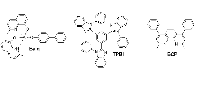
상기 정공 블로킹층 위에 전자 수송층이 진공 증착 방법, 또는 스핀 코팅 방법으로서 전자수송층(ETL)을 형성한다. 전자 수송층 재료로서는 특별히 제한되지는 않으며 Alq3를 이용할 수 있다. 상기 전자수송층의 두께는 50 내지 600Å인 것이 바람직하다. 만약 전자수송층의 두께가 50Å 미만인 경우에는 수명 특성이 저하되며, 600Å를 초과하는 경우에는 구동전압 상승으로 바람직하지 못하다.An electron transport layer forms an electron transport layer (ETL) on the hole blocking layer as a vacuum deposition method or a spin coating method. It does not restrict | limit especially as an electron carrying layer material, Alq3 can be used. It is preferable that the thickness of the said electron carrying layer is 50-600 GPa. If the thickness of the electron transport layer is less than 50 kW, the lifespan characteristics are lowered. If the electron transport layer is more than 600 kW, it is not preferable to increase the driving voltage.
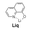
또한 상기 전자 수송층 위에 전자 주입층(EIL)이 선택적으로 적층될 수 있다. 상기 전자 주입층 형성 재료로서는 LiF, NaCl, CsF, Li2O, BaO, Liq 등의 물질을 이용할 수 있다. 상기 전자 주입층의 두께는 1 내지 100Å인 것이 바람직하다. 만약 전자주입층의 두께가 1Å 미만인 경우에는 효과적인 전자주입층으로서 역할을 못하여 구동전압이 높고, 100Å를 초과하는 경우에는 절연층으로 작용하여 구동전 압이 높아 바람직하지 못하다.In addition, an electron injection layer EIL may be selectively stacked on the electron transport layer. As the electron injection layer forming material, materials such as LiF, NaCl, CsF, Li 2 O, BaO, and Liq can be used. It is preferable that the thickness of the said electron injection layer is 1-100 kPa. If the thickness of the electron injection layer is less than 1 kW, the driving voltage is not high because it does not serve as an effective electron injection layer, and if it exceeds 100 kW, the driving voltage acts as an insulating layer.
이어서, 상기 전자주입층 상부에 제2전극인 캐소드용 금속을 진공열 증착, 스퍼터링(Sputtering), 금속-유기 화학증착법(Metal-Organic Chemical Vapor Deposition)등의 방법을 이용하여 제2전극인 캐소드를 형성함으로써 유기 전계 발광 소자가 완성된다.Subsequently, the cathode, which is the second electrode, is deposited on the electron injection layer using a method such as vacuum thermal deposition, sputtering, and metal-organic chemical vapor deposition. By forming, an organic electroluminescent element is completed.
상기 캐소드 금속으로는 리튬(Li), 마그네슘(Mg), 알루미늄(Al), 알루미늄-리튬(Al-Li), 칼슘(Ca), 마그네슘-인듐(Mg-In), 마그네슘-은(Mg-Ag) 등이 이용된다. The cathode metal is lithium (Li), magnesium (Mg), aluminum (Al), aluminum-lithium (Al-Li), calcium (Ca), magnesium-indium (Mg-In), magnesium-silver (Mg-Ag ) And the like are used.
본 발명의 유기 전계 발광 소자는 애노드, 정공주입층, 정공수송층, 발광층, 전자 수송층, 전자 주입층, 캐소드의 필요에 따라 한 층 또는 두 층의 중간층을 더 형성하거나 생략하는 것도 가능하다.The organic electroluminescent device of the present invention may further form or omit an intermediate layer of one or two layers according to the needs of the anode, the hole injection layer, the hole transport layer, the light emitting layer, the electron transport layer, the electron injection layer, and the cathode.
이하, 본 발명을 하기 실시예를 들어 설명하기로 하되, 본 발명이 하기 실시예로만 한정되는 것은 아니다.Hereinafter, the present invention will be described with reference to the following examples, but the present invention is not limited only to the following examples.
실시예 1Example 1
애노드는 코닝(corning) 15Ω/cm2 (1200Å) ITO 유리 기판을 50mm x 50mm x 0.7mm 크기로 잘라서 이소프로필 알코올과 순수 물 속에서 각 5 분 동안 초음파 세정한 후, 30분 동안 UV, 오존 세정하여 사용하였다.The anode cuts a corning 15Ω / cm 2 (1200Å) ITO glass substrate to 50mm x 50mm x 0.7mm and ultrasonically cleans for 5 minutes in isopropyl alcohol and pure water, followed by UV and ozone cleaning for 30 minutes. Was used.
상기 기판 상부에 N,N'-디(1-나프틸)-N,N'-디페닐벤지딘(N,N'-di(1-naphtyl)-N,N'-diphenylbenzidine; NPD)을 진공 증착하여 정공 수송층을 600Å 두께로 형성하였다.N, N'-di (1-naphthyl) -N, N'-diphenylbenzidine (N, N'-di (1-naphtyl) -N, N'-diphenylbenzidine (NPD)) was vacuum deposited on the substrate. Thus, a hole transport layer was formed to a thickness of 600 kPa.
상기 정공 수송층 상부에 2개의 호스트 물질인 CBP 66중량부와 BAlq 22중량부에 인광 도펀트인 Ir(pq)2(acac) 11중량부와 함께, 발광 보조제로서 1%의 트리스(2-페닐피리딘)이리듐 Ir(ppy)3 1중량부를 진공증착하여 약 400Å의 두께로 발광층을 형성하였다.66 parts by weight of two host materials CBP and 22 parts by weight of BAlq and 11 parts by weight of a phosphorescent dopant Ir (pq) 2 (acac) on top of the hole transport layer, together with 1% of tris (2-phenylpyridine) as a luminescent aid. 1 part by weight of iridium Ir (ppy) 3 was vacuum deposited to form a light emitting layer having a thickness of about 400 GPa.
상기 발광층 상부에 전자 수송 물질인 Alq3를 증착하여 약 300Å 두께의 전자 수송층을 형성하였다.Alq 3 , an electron transporting material, was deposited on the emission layer to form an electron transporting layer having a thickness of about 300 μs.
상기 전자 수송층 상부에 LiF 10Å (전자 주입층)과 Al 1000Å (캐소드)을 순차적으로 진공 증착하여 LiF/Al 전극을 형성하여 도 1에 도시한 바와 같은 유기 전계 발광 소자를 제조하였다.LiF 10 전극 (electron injection layer) and
실시예 2Example 2
발광 보조제로서 5%의 Ir(ppy)3 3중량부를 사용한 것을 제외하고는, 실시예 1과 동일한 방법에 따라 실시하여 유기 전계 발광 소자를 제조하였다.An organic electroluminescent device was manufactured in the same manner as in Example 1, except that 3 parts by weight of Ir (ppy) 3 was used as a light emission aid.
비교예 1Comparative Example 1
애노드는 코닝(corning) 15Ω/cm2 (1200Å) ITO 유리 기판을 50mm x 50mm x 0.7mm 크기로 잘라서 이소프로필 알코올과 순수 물 속에서 각 5 분 동안 초음파 세정한 후, 30분 동안 UV, 오존 세정하여 사용하였다.The anode cuts a corning 15Ω / cm 2 (1200Å) ITO glass substrate to 50mm x 50mm x 0.7mm and ultrasonically cleans for 5 minutes in isopropyl alcohol and pure water, followed by UV and ozone cleaning for 30 minutes. Was used.
상기 기판 상부에 N,N'-디(1-나프틸)-N,N'-디페닐벤지딘(N,N'-di(1-naphtyl)-N,N'-diphenylbenzidine; NPD)을 진공 증착하여 정공 수송층을 600Å 두께로 형성하였다.N, N'-di (1-naphthyl) -N, N'-diphenylbenzidine (N, N'-di (1-naphtyl) -N, N'-diphenylbenzidine (NPD)) was vacuum deposited on the substrate. Thus, a hole transport layer was formed to a thickness of 600 kPa.
상기 정공 수송층 상부에 호스트인 CBP 66중량부와 BAlq 22중량부에 인광 도펀트인 Ir(pq)2(acac) 12중량부를 진공증착하여 약 400Å의 두께로 발광층을 형성하였다.A light emitting layer was formed on the hole transport layer by vacuum depositing 12 parts by weight of phosphorescent dopant Ir (pq) 2 (acac) at 66 parts by weight of the host CBP and 22 parts by weight of BAlq.
상기 발광층 상부에 전자 수송 물질인 Alq3를 증착하여 약 300Å 두께의 전자 수송층을 형성하였다.Alq3, an electron transporting material, was deposited on the emission layer to form an electron transporting layer having a thickness of about 300 kHz.
상기 전자 수송층 상부에 LiF 10Å (전자 주입층)과 Al 1000Å (캐소드)을 순차적으로 진공 증착하여 LiF/Al 전극을 형성하여 도 1에 도시한 바와 같은 유기 전계 발광 소자를 제조하였다.LiF 10 전극 (electron injection layer) and
상기 실시예 1-2 및 비교예 1에 따라 제조된 유기 전계 발광 소자에 있어서, 발광효율, 전력 효율 및 수명 특성을 조사하였다.In the organic EL device manufactured according to Example 1-2 and Comparative Example 1, the luminous efficiency, power efficiency and lifespan characteristics were investigated.
그 결과, 실시예 1 및 실시예 2의 유기 전계 발광 소자의 휘도는 800cd/m2에서 각각 5.6cd/A 및 5.7cd/A이고, 비교예 1의 유기 전계 발광 소자의 휘도는 800cd/m2에서 4.7cd/A로서 상기 실시예들은 비교예에 비하여 효율이 개선되었다.As a result, the luminance of the organic electroluminescent elements of Examples 1 and 2 was 5.6 cd / A at 800 cd /
또한 비교예 1의 유기 전계 발광 소자의 전력효율은 2.4lm/W이고, 실시예 1 및 실시예 2의 유기 전계 발광 소자는 전력효율이 각가 2.71lm/W 및 2.95lm/W로서 비교예 1의 경우에 비하여 전력효율이 개선되었다.In addition, the power efficiency of the organic EL device of Comparative Example 1 is 2.4lm / W, the organic EL device of Example 1 and Example 2 has a power efficiency of 2.71lm / W and 2.95lm / W of Comparative Example 1 Compared to the case, the power efficiency is improved.
또한, 수명 특성은 최초 발광 휘도가 50%선까지 감소하는 시간으로 나타내는데 실시예 1의 유기 전계 발광 소자는 4,000cd/m2에서 1,500시간이고, 비교예 1의 유기 전계 발광 소자는 4,000cd/m2에서 300시간으로 나타나 실시예 1은 비교예 1의 경우에 비하여 수명 특성이 현저하게 개선됨을 확인할 수 있었다.In addition, the lifespan characteristics are represented by the time when the initial emission luminance decreases by 50%. The organic electroluminescent device of Example 1 is 1,500 hours at 4,000 cd / m 2 , and the organic electroluminescent device of Comparative Example 1 is 4,000 cd / m. It was found that 2 to 300 hours, Example 1 was significantly improved life characteristics compared to the case of Comparative Example 1.
유기발광 디바이스의 발광층 형성시 둘 이상의 호스트 및 도펀트 이외에 발광 보조제를 이용한다. 발광 보조제를 발광층에 사용함으로써 일반적인 호스트와 도펀트 사이의 직접적인 에너지 전달이외에 발광에 사용되지 못하고 없어지는 에너지를 발광 보조제를 통하여 간접적인 방식으로 다시 도펀트에 에너지를 전달시켜 발광에 이용할 수 있게 한다. 본 발명에 따른 발광 보조제를 사용함으로써 에너지 전달 효율을 증가시켜 효율 및 수명 특성을 증가시킬 수 있다.Luminescent aids are used in addition to at least two hosts and dopants in forming the light emitting layer of the organic light emitting device. By using a light emitting aid in the light emitting layer, energy that cannot be used for light emission other than the direct energy transfer between the general host and the dopant can be used for light emission by transferring energy to the dopant in an indirect manner through the light emitting aid. By using the light emission aid according to the present invention it is possible to increase the energy transfer efficiency to increase the efficiency and life characteristics.
Claims (10)
Priority Applications (1)
| Application Number | Priority Date | Filing Date | Title |
|---|---|---|---|
| KR1020040094912A KR100659072B1 (en) | 2004-11-19 | 2004-11-19 | Organic electroluminescent element |
Applications Claiming Priority (1)
| Application Number | Priority Date | Filing Date | Title |
|---|---|---|---|
| KR1020040094912A KR100659072B1 (en) | 2004-11-19 | 2004-11-19 | Organic electroluminescent element |
Publications (2)
| Publication Number | Publication Date |
|---|---|
| KR20060055766A KR20060055766A (en) | 2006-05-24 |
| KR100659072B1 true KR100659072B1 (en) | 2006-12-21 |
Family
ID=37151709
Family Applications (1)
| Application Number | Title | Priority Date | Filing Date |
|---|---|---|---|
| KR1020040094912A Expired - Lifetime KR100659072B1 (en) | 2004-11-19 | 2004-11-19 | Organic electroluminescent element |
Country Status (1)
| Country | Link |
|---|---|
| KR (1) | KR100659072B1 (en) |
Families Citing this family (1)
| Publication number | Priority date | Publication date | Assignee | Title |
|---|---|---|---|---|
| KR100732823B1 (en) * | 2005-04-21 | 2007-06-27 | 삼성에스디아이 주식회사 | Organometallic compound in which a host compound and a dopant compound are connected, an organic electroluminescent device using the same, and a manufacturing method thereof |
-
2004
- 2004-11-19 KR KR1020040094912A patent/KR100659072B1/en not_active Expired - Lifetime
Also Published As
| Publication number | Publication date |
|---|---|
| KR20060055766A (en) | 2006-05-24 |
Similar Documents
| Publication | Publication Date | Title |
|---|---|---|
| KR100751316B1 (en) | Organic electroluminescent element | |
| KR100787428B1 (en) | Organic electroluminescent element | |
| KR100708655B1 (en) | Organic electroluminescent element | |
| US8148891B2 (en) | Electron impeding layer for high efficiency phosphorescent OLEDs | |
| CN101427397B (en) | Multiple Dopant Emissive OLEDs | |
| JP4362461B2 (en) | Organic electroluminescence device | |
| KR100787423B1 (en) | Organic electroluminescent element | |
| US8330351B2 (en) | Multiple dopant emissive layer OLEDs | |
| US6902833B2 (en) | Materials and structures for enhancing the performance or organic light emitting devices | |
| US7198859B2 (en) | Materials and structures for enhancing the performance of organic light emitting devices | |
| KR100669775B1 (en) | Organic electroluminescent element | |
| KR100669790B1 (en) | Organic electroluminescent element | |
| KR20060040829A (en) | Organic electroluminescent element | |
| KR100730132B1 (en) | Organic light emitting display device | |
| KR100669776B1 (en) | Organic electroluminescent element | |
| KR100659072B1 (en) | Organic electroluminescent element | |
| KR100581918B1 (en) | Organic electroluminescent element | |
| KR100669777B1 (en) | Organic electroluminescence display |
Legal Events
| Date | Code | Title | Description |
|---|---|---|---|
| A201 | Request for examination | ||
| PA0109 | Patent application |
St.27 status event code: A-0-1-A10-A12-nap-PA0109 |
|
| PA0201 | Request for examination |
St.27 status event code: A-1-2-D10-D11-exm-PA0201 |
|
| R17-X000 | Change to representative recorded |
St.27 status event code: A-3-3-R10-R17-oth-X000 |
|
| PG1501 | Laying open of application |
St.27 status event code: A-1-1-Q10-Q12-nap-PG1501 |
|
| E902 | Notification of reason for refusal | ||
| PE0902 | Notice of grounds for rejection |
St.27 status event code: A-1-2-D10-D21-exm-PE0902 |
|
| E13-X000 | Pre-grant limitation requested |
St.27 status event code: A-2-3-E10-E13-lim-X000 |
|
| P11-X000 | Amendment of application requested |
St.27 status event code: A-2-2-P10-P11-nap-X000 |
|
| P13-X000 | Application amended |
St.27 status event code: A-2-2-P10-P13-nap-X000 |
|
| E701 | Decision to grant or registration of patent right | ||
| PE0701 | Decision of registration |
St.27 status event code: A-1-2-D10-D22-exm-PE0701 |
|
| GRNT | Written decision to grant | ||
| PR0701 | Registration of establishment |
St.27 status event code: A-2-4-F10-F11-exm-PR0701 |
|
| PR1002 | Payment of registration fee |
St.27 status event code: A-2-2-U10-U11-oth-PR1002 Fee payment year number: 1 |
|
| PG1601 | Publication of registration |
St.27 status event code: A-4-4-Q10-Q13-nap-PG1601 |
|
| PN2301 | Change of applicant |
St.27 status event code: A-5-5-R10-R11-asn-PN2301 |
|
| PN2301 | Change of applicant |
St.27 status event code: A-5-5-R10-R11-asn-PN2301 |
|
| PN2301 | Change of applicant |
St.27 status event code: A-5-5-R10-R14-asn-PN2301 |
|
| R18-X000 | Changes to party contact information recorded |
St.27 status event code: A-5-5-R10-R18-oth-X000 |
|
| R18-X000 | Changes to party contact information recorded |
St.27 status event code: A-5-5-R10-R18-oth-X000 |
|
| PR1001 | Payment of annual fee |
St.27 status event code: A-4-4-U10-U11-oth-PR1001 Fee payment year number: 4 |
|
| R18-X000 | Changes to party contact information recorded |
St.27 status event code: A-5-5-R10-R18-oth-X000 |
|
| PR1001 | Payment of annual fee |
St.27 status event code: A-4-4-U10-U11-oth-PR1001 Fee payment year number: 5 |
|
| PR1001 | Payment of annual fee |
St.27 status event code: A-4-4-U10-U11-oth-PR1001 Fee payment year number: 6 |
|
| PN2301 | Change of applicant |
St.27 status event code: A-5-5-R10-R11-asn-PN2301 |
|
| PN2301 | Change of applicant |
St.27 status event code: A-5-5-R10-R14-asn-PN2301 |
|
| FPAY | Annual fee payment |
Payment date: 20121130 Year of fee payment: 7 |
|
| PR1001 | Payment of annual fee |
St.27 status event code: A-4-4-U10-U11-oth-PR1001 Fee payment year number: 7 |
|
| FPAY | Annual fee payment |
Payment date: 20131129 Year of fee payment: 8 |
|
| PR1001 | Payment of annual fee |
St.27 status event code: A-4-4-U10-U11-oth-PR1001 Fee payment year number: 8 |
|
| R18-X000 | Changes to party contact information recorded |
St.27 status event code: A-5-5-R10-R18-oth-X000 |
|
| FPAY | Annual fee payment |
Payment date: 20141128 Year of fee payment: 9 |
|
| PR1001 | Payment of annual fee |
St.27 status event code: A-4-4-U10-U11-oth-PR1001 Fee payment year number: 9 |
|
| R18-X000 | Changes to party contact information recorded |
St.27 status event code: A-5-5-R10-R18-oth-X000 |
|
| PR1001 | Payment of annual fee |
St.27 status event code: A-4-4-U10-U11-oth-PR1001 Fee payment year number: 10 |
|
| P22-X000 | Classification modified |
St.27 status event code: A-4-4-P10-P22-nap-X000 |
|
| PR1001 | Payment of annual fee |
St.27 status event code: A-4-4-U10-U11-oth-PR1001 Fee payment year number: 11 |
|
| FPAY | Annual fee payment |
Payment date: 20171129 Year of fee payment: 12 |
|
| PR1001 | Payment of annual fee |
St.27 status event code: A-4-4-U10-U11-oth-PR1001 Fee payment year number: 12 |
|
| FPAY | Annual fee payment |
Payment date: 20181126 Year of fee payment: 13 |
|
| PR1001 | Payment of annual fee |
St.27 status event code: A-4-4-U10-U11-oth-PR1001 Fee payment year number: 13 |
|
| FPAY | Annual fee payment |
Payment date: 20191202 Year of fee payment: 14 |
|
| PR1001 | Payment of annual fee |
St.27 status event code: A-4-4-U10-U11-oth-PR1001 Fee payment year number: 14 |
|
| PR1001 | Payment of annual fee |
St.27 status event code: A-4-4-U10-U11-oth-PR1001 Fee payment year number: 15 |
|
| R18-X000 | Changes to party contact information recorded |
St.27 status event code: A-5-5-R10-R18-oth-X000 |
|
| PR1001 | Payment of annual fee |
St.27 status event code: A-4-4-U10-U11-oth-PR1001 Fee payment year number: 16 |
|
| P22-X000 | Classification modified |
St.27 status event code: A-4-4-P10-P22-nap-X000 |
|
| PR1001 | Payment of annual fee |
St.27 status event code: A-4-4-U10-U11-oth-PR1001 Fee payment year number: 17 |
|
| PR1001 | Payment of annual fee |
St.27 status event code: A-4-4-U10-U11-oth-PR1001 Fee payment year number: 18 |
|
| P22-X000 | Classification modified |
St.27 status event code: A-4-4-P10-P22-nap-X000 |
|
| PC1801 | Expiration of term |
St.27 status event code: N-4-6-H10-H14-oth-PC1801 Not in force date: 20241120 Ip right cessation event data comment text: Termination Category : EXPIRATION_OF_DURATION |
|
| P22-X000 | Classification modified |
St.27 status event code: A-4-4-P10-P22-nap-X000 |