KR100787263B1 - Rfid tag and manufacturing method thereof - Google Patents
Rfid tag and manufacturing method thereof Download PDFInfo
- Publication number
- KR100787263B1 KR100787263B1 KR1020060082845A KR20060082845A KR100787263B1 KR 100787263 B1 KR100787263 B1 KR 100787263B1 KR 1020060082845 A KR1020060082845 A KR 1020060082845A KR 20060082845 A KR20060082845 A KR 20060082845A KR 100787263 B1 KR100787263 B1 KR 100787263B1
- Authority
- KR
- South Korea
- Prior art keywords
- chip
- loop antenna
- rfid tag
- dielectric member
- chip mounting
- Prior art date
Links
- 238000004519 manufacturing process Methods 0.000 title claims abstract description 25
- 238000004804 winding Methods 0.000 claims abstract description 18
- 238000000034 method Methods 0.000 claims description 16
- 238000009413 insulation Methods 0.000 claims description 5
- 239000002184 metal Substances 0.000 abstract description 19
- 229910052751 metal Inorganic materials 0.000 abstract description 19
- 238000010586 diagram Methods 0.000 description 19
- 239000000758 substrate Substances 0.000 description 18
- 238000004891 communication Methods 0.000 description 13
- 238000006243 chemical reaction Methods 0.000 description 10
- 239000003989 dielectric material Substances 0.000 description 6
- 238000010030 laminating Methods 0.000 description 5
- 230000008859 change Effects 0.000 description 4
- 230000006870 function Effects 0.000 description 4
- 238000007747 plating Methods 0.000 description 4
- 230000008569 process Effects 0.000 description 4
- 239000000853 adhesive Substances 0.000 description 3
- 239000004020 conductor Substances 0.000 description 3
- 238000005530 etching Methods 0.000 description 3
- 229920000139 polyethylene terephthalate Polymers 0.000 description 3
- 239000005020 polyethylene terephthalate Substances 0.000 description 3
- 239000011347 resin Substances 0.000 description 3
- 229920005989 resin Polymers 0.000 description 3
- 239000004642 Polyimide Substances 0.000 description 2
- 230000001070 adhesive effect Effects 0.000 description 2
- 230000005684 electric field Effects 0.000 description 2
- 230000005672 electromagnetic field Effects 0.000 description 2
- 239000011521 glass Substances 0.000 description 2
- 238000013507 mapping Methods 0.000 description 2
- 229920001721 polyimide Polymers 0.000 description 2
- 229920001955 polyphenylene ether Polymers 0.000 description 2
- -1 polytetrafluoroethylene Polymers 0.000 description 2
- 229920001343 polytetrafluoroethylene Polymers 0.000 description 2
- 239000004810 polytetrafluoroethylene Substances 0.000 description 2
- 238000007639 printing Methods 0.000 description 2
- 238000003672 processing method Methods 0.000 description 2
- 230000001681 protective effect Effects 0.000 description 2
- RYGMFSIKBFXOCR-UHFFFAOYSA-N Copper Chemical compound [Cu] RYGMFSIKBFXOCR-UHFFFAOYSA-N 0.000 description 1
- 229910000831 Steel Inorganic materials 0.000 description 1
- 238000005452 bending Methods 0.000 description 1
- 230000008901 benefit Effects 0.000 description 1
- 230000005540 biological transmission Effects 0.000 description 1
- 239000003990 capacitor Substances 0.000 description 1
- 229910052802 copper Inorganic materials 0.000 description 1
- 239000010949 copper Substances 0.000 description 1
- 230000008878 coupling Effects 0.000 description 1
- 238000010168 coupling process Methods 0.000 description 1
- 238000005859 coupling reaction Methods 0.000 description 1
- 238000013461 design Methods 0.000 description 1
- 230000006866 deterioration Effects 0.000 description 1
- 230000000694 effects Effects 0.000 description 1
- 230000001747 exhibiting effect Effects 0.000 description 1
- 238000000465 moulding Methods 0.000 description 1
- 239000004033 plastic Substances 0.000 description 1
- 229920003023 plastic Polymers 0.000 description 1
- 239000011112 polyethylene naphthalate Substances 0.000 description 1
- 239000004800 polyvinyl chloride Substances 0.000 description 1
- 238000012545 processing Methods 0.000 description 1
- 238000007650 screen-printing Methods 0.000 description 1
- 238000004088 simulation Methods 0.000 description 1
- 239000007787 solid Substances 0.000 description 1
- 239000010959 steel Substances 0.000 description 1
- 229920001169 thermoplastic Polymers 0.000 description 1
- 239000004416 thermosoftening plastic Substances 0.000 description 1
Images


Classifications
-
- G—PHYSICS
- G06—COMPUTING; CALCULATING OR COUNTING
- G06K—GRAPHICAL DATA READING; PRESENTATION OF DATA; RECORD CARRIERS; HANDLING RECORD CARRIERS
- G06K19/00—Record carriers for use with machines and with at least a part designed to carry digital markings
- G06K19/06—Record carriers for use with machines and with at least a part designed to carry digital markings characterised by the kind of the digital marking, e.g. shape, nature, code
- G06K19/067—Record carriers with conductive marks, printed circuits or semiconductor circuit elements, e.g. credit or identity cards also with resonating or responding marks without active components
- G06K19/07—Record carriers with conductive marks, printed circuits or semiconductor circuit elements, e.g. credit or identity cards also with resonating or responding marks without active components with integrated circuit chips
- G06K19/077—Constructional details, e.g. mounting of circuits in the carrier
- G06K19/07749—Constructional details, e.g. mounting of circuits in the carrier the record carrier being capable of non-contact communication, e.g. constructional details of the antenna of a non-contact smart card
- G06K19/07773—Antenna details
- G06K19/07786—Antenna details the antenna being of the HF type, such as a dipole
-
- H—ELECTRICITY
- H01—ELECTRIC ELEMENTS
- H01Q—ANTENNAS, i.e. RADIO AERIALS
- H01Q1/00—Details of, or arrangements associated with, antennas
- H01Q1/12—Supports; Mounting means
- H01Q1/22—Supports; Mounting means by structural association with other equipment or articles
-
- H—ELECTRICITY
- H01—ELECTRIC ELEMENTS
- H01Q—ANTENNAS, i.e. RADIO AERIALS
- H01Q1/00—Details of, or arrangements associated with, antennas
- H01Q1/12—Supports; Mounting means
- H01Q1/22—Supports; Mounting means by structural association with other equipment or articles
- H01Q1/2208—Supports; Mounting means by structural association with other equipment or articles associated with components used in interrogation type services, i.e. in systems for information exchange between an interrogator/reader and a tag/transponder, e.g. in Radio Frequency Identification [RFID] systems
- H01Q1/2225—Supports; Mounting means by structural association with other equipment or articles associated with components used in interrogation type services, i.e. in systems for information exchange between an interrogator/reader and a tag/transponder, e.g. in Radio Frequency Identification [RFID] systems used in active tags, i.e. provided with its own power source or in passive tags, i.e. deriving power from RF signal
-
- H—ELECTRICITY
- H01—ELECTRIC ELEMENTS
- H01Q—ANTENNAS, i.e. RADIO AERIALS
- H01Q7/00—Loop antennas with a substantially uniform current distribution around the loop and having a directional radiation pattern in a plane perpendicular to the plane of the loop
-
- H—ELECTRICITY
- H01—ELECTRIC ELEMENTS
- H01Q—ANTENNAS, i.e. RADIO AERIALS
- H01Q7/00—Loop antennas with a substantially uniform current distribution around the loop and having a directional radiation pattern in a plane perpendicular to the plane of the loop
- H01Q7/04—Screened antennas
Landscapes
- Engineering & Computer Science (AREA)
- Computer Hardware Design (AREA)
- Microelectronics & Electronic Packaging (AREA)
- Physics & Mathematics (AREA)
- General Physics & Mathematics (AREA)
- Theoretical Computer Science (AREA)
- Computer Networks & Wireless Communication (AREA)
- Details Of Aerials (AREA)
- Near-Field Transmission Systems (AREA)
- Credit Cards Or The Like (AREA)
Abstract
금속에 접착해도 필요한 전력을 공급할 수 있음과 함께 전자파를 송신할 수 있고, 게다가 높은 권취 정밀도가 필요하지 않는 루프 안테나 구성의 RFID 태그 및 그 제조 방법을 제공한다. 루프 안테나를 구비한 RFID 태그로서, 평판 형상의 유전체 부재(51)와, 그 유전체 부재의 제1 면과 제2 면에서 소정의 간극을 두고 형성되며, 또한, 그 유전체 부재의 제1 면부터 제2 면까지 각각 연통하는 제1, 제2 루프 안테나 패턴(52, 53)과, 한 쪽의 면에서 제1, 제2 루프 안테나 패턴(52, 53)에 전기적으로 접속하는 IC 칩(54)을 구비하고 있다. The present invention provides an RFID tag having a loop antenna configuration and a method of manufacturing the same, which can supply necessary electric power even when bonded to metal, transmit electromagnetic waves, and do not require high winding accuracy. An RFID tag having a loop antenna, which is formed with a flat dielectric member 51 and a predetermined gap between the first and second surfaces of the dielectric member, and is formed from the first surface of the dielectric member. First and second loop antenna patterns 52 and 53 communicating to two surfaces, respectively, and IC chip 54 electrically connected to the first and second loop antenna patterns 52 and 53 on one surface thereof. Equipped.
루프 안테나, 태그, 유전체 부재, 간극, IC 칩 Loop antenna, tag, dielectric member, gap, IC chip
Description
도 1은 본 발명의 루프 안테나 구성의 RFID 태그의 분해 사시도. 1 is an exploded perspective view of an RFID tag in a loop antenna configuration of the present invention.
도 2는 제1 실시예의 RFID 태그의 평면도. Fig. 2 is a plan view of the RFID tag of the first embodiment.
도 3은 제1 실시예의 RFID 태그의 이면도. Fig. 3 is a rear view of the RFID tag of the first embodiment.
도 4는 절연층(도시하지 않음)을 개재하여 본 발명의 RFID 태그를 도전성 물체에 접착한 경우의 등가 안테나 회로를 도시하는 도면. Fig. 4 is a diagram showing an equivalent antenna circuit when the RFID tag of the present invention is adhered to a conductive object via an insulating layer (not shown).
도 5는 본 발명의 RFID 태그의 제조 방법 설명도. 5 is an explanatory diagram of a manufacturing method of an RFID tag according to the present invention.
도 6은 태그 안테나의 임피던스를 스미스 차트 상에 플롯한 도면. 6 is a plot of the impedance of a tag antenna on a Smith chart.
도 7은 RFID 태그의 등가 회로를 도시하는 도면. Fig. 7 is a diagram showing an equivalent circuit of an RFID tag.
도 8은 주파수를 800㎒∼1.1㎓(1100㎒)의 사이에서 변화시켰을 때의 안테나 게인 특성을 도시하는 도면. 8 shows antenna gain characteristics when the frequency is changed between 800 MHz and 1.1 GHz (1100 MHz).
도 9는 종래의 RFID 태그의 안테나 게인 특성으로, 비교하기 위해서 제1 실시예의 안테나 게인 특성을 나열하여 도시하는 도면. Fig. 9 is a diagram showing the antenna gain characteristics of a conventional RFID tag, in which antenna gain characteristics of the first embodiment are listed for comparison.
도 10은 종래의 RFID 태그의 평면도 및 이면도. 10 is a plan view and a rear view of a conventional RFID tag.
도 11은 본 발명의 안테나 패턴 설명도. 11 is an explanatory diagram of an antenna pattern of the present invention.
도 12는 본 발명의 s2를 변경했을 때의 게인 특성, 칩 용량 특성, 태그 안테 나 저항 특성을 도시하는 도면. Fig. 12 is a diagram showing gain characteristics, chip capacitance characteristics, and tag antenna resistance characteristics when s2 of the present invention is changed.
도 13은 제1 실시예의 RFID 태그의 효과 설명도. Fig. 13 is a diagram for explaining the effect of the RFID tag of the first embodiment.
도 14는 권취 오차와 게인 변화의 대응도. 14 is a correspondence diagram between winding error and gain change.
도 15는 제2 실시예의 루프 안테나 구성의 RFID 태그의 설명도. Fig. 15 is an illustration of an RFID tag in a loop antenna configuration of the second embodiment.
도 16은 제2 실시예의 태그 안테나의 임피던스를 스미스 차트 상에 플롯한 도면. Fig. 16 is a plot of the impedance of the tag antenna of the second embodiment on a Smith chart.
도 17은 주파수를 800㎒∼1.1㎓(1100㎒)의 사이에서 변화시켰을 때의 제2 실시예의 태그 안테나의 안테나 게인 특성을 도시하는 도면. Fig. 17 is a diagram showing the antenna gain characteristics of the tag antenna of the second embodiment when the frequency is changed between 800 MHz and 1.1 GHz (1100 MHz).
도 18은 RFID 태그의 문제점 설명도. 18 is a problem explanatory diagram of an RFID tag.
도 19는 종래의 RFID 태그의 문제점 설명도. 19 is a diagram for explaining a problem of a conventional RFID tag.
도 20은 종래의 RFID 태그의 사시도. 20 is a perspective view of a conventional RFID tag.
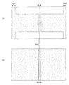
도 21은 도 20의 RFID 태그의 도전성 물체에의 접착 설명도. 21 is an explanatory diagram of adhesion of the RFID tag of FIG. 20 to a conductive object;
도 22는 도 20의 RFID 태그를 금속 물체에 접착해도 LSI 칩에 필요한 전력을 공급할 수 있고, 또한, 전자파를 송신할 수 있는 이유 설명도. Fig. 22 is an explanatory diagram illustrating why electric power required for the LSI chip can be supplied and electromagnetic waves can be transmitted even if the RFID tag of Fig. 20 is adhered to a metal object.
도 23은 도 20의 RFID 태그의 제조 방법 설명도(그 1). 23 is an explanatory diagram of a method of manufacturing the RFID tag of FIG. 20 (part 1).
도 24는 도 20의 RFID 태그의 제조 방법 설명도(그 2). 24 is an explanatory diagram of a manufacturing method of the RFID tag of FIG. 20 (No. 2).
<도면의 주요부분에 대한 부호의 설명><Description of the symbols for the main parts of the drawings>
50: RFID 태그50: RFID Tag
51: 유전체 기판51: dielectric substrate
52, 53: 제1, 제2 루프 안테나 부분52, 53: first and second loop antenna portions
54: LSI 칩54: LSI chip
55, 56: 칩 탑재 패드55, 56: chip-mount pad
[특허 문헌1] 일본 특허 공개 2002-298106호 공보[Patent Document 1] Japanese Unexamined Patent Publication No. 2002-298106
[특허 문헌2] 일본 특허 공개 2006-53833[Patent Document 2] Japanese Patent Laid-Open 2006-53833
본 발명은, RFID 태그 및 그 제조 방법에 관한 것으로, 특히 루프 안테나를 구비하고, 도전성 물체 혹은 비도전성 물체에 접착해서 사용해도 태그 안테나로서의 소요 특성을 발휘하는 RFID 태그 및 그 제조 방법에 관한 것이다. BACKGROUND OF THE
종래, 유통업계, 운송업계 등에서, 개개의 제품 정보를 관리하는 방법으로서, 제품 자체에, 혹은 제품의 상자에 바코드를 인쇄 혹은 첨부하고, 이 바코드를 바코드 리더에 의해 판독하는 방법이 널리 이용되고 있다. 그러나, 이러한 바코드 처리 방법에서는, 바코드를 판독할 때, 바코드 리더를 바코드에 접촉시켜야 되어, 판독 작업이 번거로웠다. 또한 종래의 바코드 처리 방법에서는, 바코드 자체에 새로운 정보를 추가 혹은 갱신할 수 없는 문제가 있었다. Background Art Conventionally, in the distribution industry, the transportation industry, and the like, as a method of managing individual product information, a method of printing or attaching a barcode to the product itself or to a box of the product and reading the barcode by a barcode reader is widely used. However, in such a barcode processing method, when reading a barcode, the barcode reader must be brought into contact with the barcode, which makes reading work cumbersome. In the conventional barcode processing method, there is a problem in that new information cannot be added or updated in the barcode itself.
이 때문에, 최근, 바코드 대신에 물품 등에 RFID(Radio Frequency Identification) 태그를 붙이고, 물품의 정보를 무선(전자 결합)으로 비접촉에 의해 판독하는 것이 요구되며, 실용화되고 있다. RFID 태그는, IC 카드의 기능에 정 보의 무선 통신 기능을 추가한 것으로, 정보 기록 가능한 불휘발성 메모리를 구비하고 있지만 전지(전원부)를 갖고 있지 않다. 이 때문에, 태그 판독 장치는 RFID 태그의 메모리로부터 정보를 비접촉으로 판독할 때, 전자파에 의해 RFID 태그에 전력을 공급하고, 그 메모리로부터 정보를 판독하게 되어 있다. 이러한 RFID 태그에 의하면, 작업성의 대폭적인 향상을 도모할 수 있고, 게다가, RFID 태그와의 사이에서 인증 기능, 암호화 등의 기술을 이용함으로써, 우수한 시큐러티를 확보할 수 있다. For this reason, in recent years, RFID (Radio Frequency Recognition) identification tags are attached to articles instead of barcodes, and information of articles is read wirelessly (electromagnetic coupling) by non-contact, and has been put into practical use. The RFID tag adds a wireless communication function of information to the function of the IC card, and has a nonvolatile memory capable of recording information, but does not have a battery (power supply unit). Therefore, when the tag reading device reads information from the RFID tag's memory in a non-contact manner, the tag reading device supplies electric power to the RFID tag by electromagnetic waves and reads the information from the memory. According to such an RFID tag, the workability can be greatly improved, and excellent security can be secured by using a technique such as an authentication function and encryption with the RFID tag.
도 18은 RFID 태그의 설명도로서, 판독 장치(1)는 안테나(2)로부터 송신 데이터에 의해 변조한 무선 신호(전자파)를 RFID 태그(3)에 송신한다. 무선 태그(3)의 안테나(3a)는 수신 신호를 정류 회로(3b)와 변복조 회로(3c)에 입력한다. 정류 회로(3b)는 무선 신호를 직류 전압으로 변환해서 변복조 회로(3c)와 논리 회로(3d)에 공급하고, 전원으로서 동작한다. 변복조 회로(3c)는 판독 장치(1)로부터 보내져 온 제어 데이터를 복조하여, 논리 회로(3d)에 입력한다. 논리 회로(3d)는 그 제어 데이터(커맨드)에 따른 논리 처리를 행하여, 예를 들면 내장의 메모리에 기억되어 있는 정보를 판독해서 변복조 회로(3c)에 입력한다. 변복조 회로(3c)는 논리 회로로부터 입력된 정보를 이용하여 반송파를 변조해서 무선으로 안테나(3a)로부터 판독 장치(1)에 송신한다. 18 is an explanatory diagram of an RFID tag, in which the
RFID 태그로서 다양한 타입이 제안되어 있다. 그 하나로서 플라스틱이나 종이 등의 유전체 베이스 시트 상에 전파 통신용의 안테나 패턴과 IC 칩(LSI)을 탑재 한 것이 있다. 이러한 RFID 태그는 비도전성의 물체에 접착되는 통신 거리 등에 관해서 소요의 성능이 얻어진다. 그러나, 스틸 등의 금속에 접착되는 경우, 그 금속에 의해 RFID 태그의 통신용 전파가 저해되어 통신 거리의 저하 등의 문제점이 발생한다. Various types have been proposed as RFID tags. One of them is an antenna pattern for radio wave communication and an IC chip (LSI) mounted on a dielectric base sheet such as plastic or paper. Such an RFID tag has a required performance with respect to a communication distance and the like adhered to a non-conductive object. However, when bonded to a metal such as steel, the radio waves for communication of the RFID tag are inhibited by the metal, which causes problems such as a decrease in communication distance.
도 19는 이러한 문제점 발생의 설명도이고, 도 19의 (a)는 반파장의 다이폴 안테나 패턴을 구비한 RFID 태그를 비도전성 물체(도시하지 않음)에 접착한 경우의 설명도로서, 리더 라이터의 안테나로부터 방사되는 전파에 의해 다이폴 안테나 DP에 IC 칩에 필요한 전력(개방 전압 V)이 발생한다. 또한, 다이폴 안테나에 전류 I를 흘려서 리더 라이터의 안테나를 향해서 전자파를 송신할 수 있다. FIG. 19 is an explanatory diagram of the occurrence of such a problem, and FIG. 19A is an explanatory diagram when an RFID tag having a half-wavelength dipole antenna pattern is attached to a non-conductive object (not shown), and the antenna of the reader / writer. The radio waves radiated from generate power (opening voltage V) required for the IC chip in the dipole antenna DP. In addition, the electromagnetic wave can be transmitted toward the antenna of the reader / writer by flowing a current I through the dipole antenna.
그러나, 금속 물체에 다이폴 안테나 패턴을 구비한 RFID 태그를 접착한 경우, 금속 표면에서 전계의 접선 방향 성분이 경계 조건으로부터 0으로 되어, 주위 전계가 0으로 된다. 이 때문에, RFID 태그의 IC 칩에 필요한 전력을 공급할 수 없다. 또한 태그 안테나로부터 리더 라이터의 안테나를 향해 전자파를 송신(산란)할 수도 없다. 즉, 도 19의 (b)에 도시한 바와 같이, 금속 물체 MTL에 다이폴 안테나 DP를 구비한 RFID 태그를 접착했을 경우, 다이폴 안테나 DP에 전류 I를 흘리면, 사상(寫像) 원리에 의해 금속 물체 MTL에 역방향으로 전류가 흐르는 이미지 IMG가 발생한다. 이 이미지에 의해, 다이폴 안테나 전류 I가 발생하는 전자계가 부정되어, RFID 태그의 IC 칩에 필요한 전력을 공급할 수 없으며, 게다가, 태그 안테나로부터 리더 라이터의 안테나를 향해 전자파를 송신할 수도 없게 된다. 이상으로부터 금속 표면에 접착해도 안테나 이득이 열화되지 않아, 전자파의 송수신이 가능한 태그 안테나를 구비한 RFID 태그가 요망된다. However, when an RFID tag having a dipole antenna pattern is attached to a metal object, the tangential component of the electric field on the metal surface becomes zero from the boundary condition, and the surrounding electric field becomes zero. For this reason, the electric power required for the IC chip of the RFID tag cannot be supplied. Further, electromagnetic waves cannot be transmitted (scattered) from the tag antenna toward the reader / writer antenna. That is, as shown in Fig. 19B, when the RFID tag having the dipole antenna DP is bonded to the metal object MTL, when the current I flows through the dipole antenna DP, the metal object is driven according to the mapping principle. An image IMG occurs with current flowing in the reverse direction to the MTL. By this image, the electromagnetic field from which the dipole antenna current I is generated is denied, so that power required for the IC chip of the RFID tag cannot be supplied, and also electromagnetic waves cannot be transmitted from the tag antenna to the antenna of the reader / writer. As mentioned above, even if it adheres to a metal surface, antenna gain does not deteriorate, and the RFID tag provided with the tag antenna which can transmit and receive electromagnetic waves is desired.
따라서, 도 19의 (c)에 도시한 바와 같이, 금속 물체 MTL 표면부터 다이폴 안테나 패턴 DP까지의 거리 D를 크게 해서 이미지의 영향을 저감시키는 것이 생각되어지지만 RFID 태그의 두께가 커져 사용상의 문제가 발생한다. 또한, UHF대의 RFID 시스템은 다른 주파수대에 비하여, 통신 거리가 길다고 하는 이점을 갖지만, UHF대의 다이폴형 태그 안테나는 보통 반파장(약 16㎝) 정도의 길이가 필요하다. 이 길이는 태그 안테나를 유전체에 접착하거나 절곡하거나 함으로써 확보하며, 또한 소형화하고 있지만, 협대역으로 된다. 이상으로부터, RFID 태그의 소형화, 및 소형화하더라도 안테나 이득이 열화되지 않고, 게다가, 최대한 대역이 넓어지는 태그 안테나를 구비한 RFID 태그가 요망된다. Therefore, as shown in FIG. 19 (c), it is considered to reduce the influence of the image by increasing the distance D from the metal object MTL surface to the dipole antenna pattern DP, but the thickness of the RFID tag increases, which causes problems in use. Occurs. In addition, the RFID system of the UHF band has the advantage that the communication distance is longer than other frequency bands, but the dipole-type tag antenna of the UHF band usually requires a length of about half-wave length (about 16 cm). This length is secured by adhering or bending the tag antenna to the dielectric, and further downsizing, but it becomes narrow band. As mentioned above, even if the RFID tag is downsized and downsized, the antenna gain does not deteriorate, and in addition, there is a demand for an RFID tag having a tag antenna that has a wider band.
또한, 태그 안테나의 수신 전력을 LSI 칩에 효율적으로 공급하기 위해서 태그 안테나와 LSI 칩의 임피던스가 매칭(정합)하고 있을 필요가 있다. 이 때문에, 임피던스 변환 회로가 필요하게 되지만, RFID 태그의 제조 코스트가 높아진다. 이 때문에, 임피던스 변환 회로를 사용하지 않고 태그 LSI 칩과 태그 안테나의 정합을 취할 필요가 있다. 즉, 임피던스 변환 회로를 사용하지 않아도 LSI 칩과의 임피던스 정합이 취해지도록 한 태그 안테나를 구비한 RFID 태그가 요망된다. In addition, in order to efficiently supply the received power of the tag antenna to the LSI chip, the impedance of the tag antenna and the LSI chip needs to be matched (matched). For this reason, an impedance conversion circuit is required, but the manufacturing cost of an RFID tag becomes high. For this reason, it is necessary to match tag LSI chip and tag antenna, without using an impedance conversion circuit. In other words, there is a need for an RFID tag provided with a tag antenna such that impedance matching with an LSI chip can be achieved without using an impedance conversion circuit.
종래의 다이폴 안테나를 구비한 RFID 태그는 상기와 같이 금속에 접착하면 통신 거리가 열화된다는 문제가 있다. 이 때문에, UHF대에서도 몇 개의 금속 대응 태그 안테나가 개발되어 있지만(특허 문헌1 참조), 모두 두께 4㎜ 이상, 길이 10㎝ 이상으로 큰 것뿐이었다. A conventional RFID tag having a dipole antenna has a problem in that a communication distance is deteriorated when the RFID tag is attached to a metal as described above. For this reason, although some metal-adaptive tag antennas were developed also in UHF band (refer patent document 1), they were all large only 4 mm or more in thickness and 10 cm or more in length.
이 때문에, 본원 출원인은, 금속 표면에 접착해도 전자파의 송수신이 가능한 소형 안테나를 구비한 RFID 태그를 제안하고 있다(특허 문헌2 참조). 이 제안된 RFID 태그(10)는, 도 20에 도시한 바와 같이, 직방체 형상의 유전체 부재(11)와, 이 유전체 부재(11)의 표면에 설치되고 루프 안테나를 형성하는 송수신용의 안테나 패턴(12)과, 이 안테나 패턴(12)에 칩 탑재 패드(13)를 개재하여 전기적으로 접속된 IC 칩(15)을 구비하고 있다. For this reason, the applicant of this application proposes the RFID tag provided with the small antenna which can transmit and receive electromagnetic waves even if it adheres to a metal surface (refer patent document 2). As shown in Fig. 20, the proposed
직방체 형상의 유전체 부재(11)는, 소정의 유전율을 갖고 있으며, 글래스 등을 포함한 수지에 의해 형성된 기판, 소위 고주파용 기판을 이용할 수 있다. 유전체 부재(11)의 평면 부분의 안테나 패턴(12)은, 도체(예를 들면, 구리 등의 금속 도체)를 에칭함으로써 형성되어 있다. 또한, IC 칩(15)을 안테나 패턴(12)에 전기적으로 접속하기 위한 한 쌍의 칩 탑재 패드(13)가, 이 안테나 패턴(12)과 함께, 상기 에칭에 의해 동시 형성되어 있다. 또한, 유전체 부재(11)의 측면 부분(두께를 형성하는 부분)의 안테나 패턴(12')은, 공지의 소위 도금에 의한 측면 도통법에 의해 형성되어 있다. IC 칩(15)은, 비접촉에 의해 정보를 기록하고, 또한 판독하기 위한 통신 회로와 메모리 및 소정의 제어 회로를 구비함과 함께, 안테나 패턴(12)에 연장되어 설치된 상기 칩 탑재 패드(13)와 전기적으로 접속하기 위한 칩 전극(도시하지 않음)을 구비하고 있다. 이상과 같이 구성된 RFID 태그(10)는, 도 21에 도시한 바와 같이, 예를 들면 금속성 물체 MTL에 절연성 접착제(예를 들면, 양면 테이프)(16) 등을 이용해서 첨부되고, 도시하지 않은 소정의 보호 필름 등에 의해 피복되어 사용된다. 또한, 이 RFID 태그(10)는, 사용할 물품에 첨부하기 위한 상기 접착제(16)나 상기 보호 필름 등을 미리 구비해서 구성되어 있어도 된다. The rectangular
이 루프 안테나 구성의 RFID 태그에 의하면, 루프 안테나에 전류 I를 흘리면, 도 19의 (b)와 마찬가지로 사상 원리에 의해 금속 물체 MTL에 도 22에 도시한 바와 같이 이미지 IMG가 발생한다. 그러나, 루프 안테나에서는 이 이미지 IMG에 의해 RFID 태그의 하측의 전류가 부정될 뿐이며, 등가적으로 일점쇄선으로 도시한 바와 같은 전류 I'가 흐르고 있다고 간주되어, RFID 태그의 LSI 칩(15)에 필요한 전력을 공급할 수 있으며, 게다가, 루프 안테나로부터 리더 라이터의 안테나를 향해 전자파를 송신할 수 있다. According to the RFID tag having the loop antenna configuration, when the current I flows through the loop antenna, the image IMG is generated in the metal object MTL as shown in Fig. 22 by the mapping principle as in Fig. 19B. However, in the loop antenna, the current of the lower side of the RFID tag is only negated by this image IMG, and equivalently, the current I 'as shown by the dashed-dotted line is considered to flow, which is necessary for the
상기 루프 안테나 구성의 RFID 태그를 제조하기 위해서는, 우선, 양면이 도전체로 피복된 프린트 기판(유전체 부재)(11)의 표면을 에칭 가공해서 도 20에 도시하는 안테나 패턴을 형성하고, 이어서, 측면에 도금 가공을 실시하여, 그 도금(12')에 의해 기판의 상면 안테나 패턴과 하면 안테나 패턴을 접속해서 루프 안테나를 형성한다(루프 안테나 형성 공정). 그런 다음, 상기 칩 탑재 패드(13)에 IC 칩(15)의 칩 전극이 전기적으로 접속하도록, 그 IC 칩(15)을 실장한다. 실장 기술로서는, 예를 들면 소위 플립 칩 실장을 채용할 수 있다. In order to manufacture the RFID tag of the loop antenna configuration, first, the surface of the printed substrate (dielectric member) 11 coated on both sides with a conductor is etched to form the antenna pattern shown in FIG. The plating process is performed, and the plating 12 'connects the upper and lower antenna patterns of the substrate to form a loop antenna (loop antenna forming step). Then, the
다른 제조 방법으로서 도 23에 도시한 바와 같이 절연성의 필름(20) 상에 안테나 패턴(12) 및 칩 탑재 패드(13)를 인쇄하고, 도 24에 도시한 바와 같이 그 필름(20)을 유전체 부재(11)에 권취하여 고정하며, 그런 다음, IC 칩(15)을 칩 탑재 패드(13)에 실장한다. As another manufacturing method, as shown in FIG. 23, the
상기 종래의 루프 안테나 구성의 RFID 태그에 의하면 소형, 박형의 구조임에 도 불구하고, 금속 표면에 접착해도 전자파의 송수신이 가능해서 통신 거리를 길게 할 수 있고, 게다가, 넓은 대역에서 게인을 거의 일정하게 할 수 있으며, 또한, 임피던스 변환 회로가 없어도 정합을 취할 수 있다. According to the conventional RFID tag of the loop antenna configuration, although the structure is small and thin, it is possible to transmit and receive electromagnetic waves even by adhering to the metal surface, so that the communication distance can be increased, and the gain is almost constant in a wide band. In addition, matching can be achieved even without an impedance conversion circuit.
그러나, 종래의 RFID 태그의 제1 제조 방법에서는, 프린트 기판을 사용하고, 게다가, 에칭 가공, 측면 도금 가공 등의 복잡한 공정이 필요하여, 제조 코스트가 높아지는 문제가 있다. 또한, 종래의 RFID 태그의 제2 제조 방법에서는, 절연 필름(20)을 유전체 부재(11)에 권취하고나서 IC 칩(15)을 실장해야 되어, 절연 필름을 유전체 재료에 권취하여 고정할 때에 높은 권취 위치 정밀도가 요구된다. 즉, IC 칩은 매우 작기 때문에, 예를 들면 0.4㎟으로 작기 때문에, 정확하게 실장하기 위해서는 높은 위치 정밀도, 예를 들면 수십∼수백㎛의 위치 정밀도로 절연 필름을 유전체 부재(11)에 권취할 필요가 있다. However, the conventional manufacturing method of the RFID tag uses a printed board, requires a complicated process such as an etching process, a side plating process, and the like, resulting in a high manufacturing cost. In the second manufacturing method of the conventional RFID tag, the
이상으로부터 본 발명의 목적은, IC 칩을 실장하고나서 필름을 유전체 재료에 권취함으로써 높은 권취 위치 정밀도가 필요하지 않는 루프 안테나 구성의 RFID 태그 및 그 제조 방법을 제공하는 것이다. As mentioned above, the objective of this invention is providing the RFID tag of the loop antenna structure which does not require a high winding position precision by mounting a film to dielectric material after mounting an IC chip, and its manufacturing method.
본 발명의 다른 목적은, 금속에 접착해도 필요한 전력을 공급할 수 있음과 함께 전자파를 송수신할 수 있고, 게다가, 대역을 넓게 할 수 있으며, 또한 임피던스 변환 회로가 불필요한 소형이면서 박형인 RFID 태그를 제공하는 것이다. Another object of the present invention is to provide a small and thin RFID tag capable of supplying necessary electric power even when bonded to a metal, transmitting and receiving electromagnetic waves, widening a band, and eliminating the need for an impedance conversion circuit. .
본 발명의 다른 목적은, 비도전성 물체에 접착해도 필요한 전력을 공급할 수 있음과 함께 전자파를 송수신할 수 있고, 게다가, 대역을 넓게 할 수 있으며, 또한 임피던스 변환 회로가 불필요한 소형이면서 박형인 RFID 태그를 제공하는 것이다. Another object of the present invention is to provide a small and thin RFID tag capable of supplying necessary electric power even when adhering to a nonconductive object, transmitting and receiving electromagnetic waves, widening a band, and eliminating the need for an impedance conversion circuit. It is.
· RFID 태그 RFID tag
본 발명의 제1 양태인 루프 안테나를 구비한 RFID 태그는, 평판 형상의 유전체 부재와, 그 유전체 부재의 제1 면과 제2 면에서 소정의 간극을 두고 형성되며, 또한, 그 유전체 부재의 제1 면부터 제2 면까지 각각 연통하는 제1, 제2 루프 안테나 패턴과, 상기 한 쪽의 면에서 상기 제1, 제2 루프 안테나 패턴에 전기적으로 접속된 IC 칩을 구비하고 있다. 상기 제1, 제2 루프 안테나 패턴은 상기 IC 칩을 탑재하는 IC 칩 탑재 부분을 구비하고, 그 IC 칩 탑재 부분을 마주 향하게 하여 소정의 간극을 두고 상기 유전체 부재에 형성된다. An RFID tag having a loop antenna as a first aspect of the present invention is formed with a flat dielectric member and a predetermined gap between the first and second surfaces of the dielectric member, and further includes a dielectric member of the dielectric member. A first and a second loop antenna pattern communicating from one surface to a second surface, respectively, and an IC chip electrically connected to the first and second loop antenna patterns from one surface. The first and second loop antenna patterns have an IC chip mounting portion for mounting the IC chip, and are formed in the dielectric member with a predetermined gap facing the IC chip mounting portion.
본 발명의 제2 양태인 루프 안테나를 구비한 RFID 태그는, 평판 형상의 유전체 부재와, IC 칩 탑재 부분을 구비한 띠 형상의 제1, 제2 루프 안테나 패턴이 그 IC 칩 탑재 부분을 마주 향하게 하여 소정의 간극을 두고 형성된 절연 필름과, 상기 IC 칩 탑재 부분에 탑재되고, 상기 제1, 제2 루프 안테나 패턴에 전기적으로 접속된 IC 칩을 구비하고, 상기 IC 칩이 탑재된 절연 필름을 상기 유전체 부재에, 그 IC 칩이 그 유전체 부재의 제1 면에 위치하도록, 또한, 제2 면에서 상기 제1, 제2 루프 안테나 패턴이 소정의 간극을 두고 위치하도록, 권취하여 구성되어 있다. The RFID tag including the loop antenna according to the second aspect of the present invention has a flat dielectric member and a strip-shaped first and second loop antenna patterns provided with an IC chip mounting portion facing the IC chip mounting portion. And an insulating film formed with a predetermined gap and an IC chip mounted on the IC chip mounting portion and electrically connected to the first and second loop antenna patterns, wherein the insulating film on which the IC chip is mounted is provided. The dielectric member is wound up so that the IC chip is located on the first surface of the dielectric member and the first and second loop antenna patterns are positioned with a predetermined gap on the second surface.
본 발명의 제3 양태인 루프 안테나를 구비한 RFID 태그는, 평판 형상의 유전체 부재와, 그 유전체 부재의 제1 면과 제2 면에서 소정의 간극을 두고 형성되며, 또한, 그 유전체 부재의 제1 면부터 제2 면까지 각각 연통하는 제1, 제2 루프 안테나 패턴과, 상기 한 쪽의 면에서 상기 제1, 제2 루프 안테나 패턴에 전기적으로 접 속된 IC 칩과, 상기 IC 칩 탑재면과 반대의 면에 적층된 절연층과 도전층을 구비하고 있다. 상기 제1, 제2 루프 안테나 패턴은 상기 IC 칩을 탑재하는 IC 칩 탑재 부분을 구비하고, 그 IC 칩 탑재 부분을 마주 향하게 하여 소정의 간극을 두고 상기 유전체 부재에 형성된다. The RFID tag with a loop antenna according to the third aspect of the present invention is formed with a flat dielectric member and a predetermined gap between the first and second surfaces of the dielectric member, and further comprising the dielectric member of the dielectric member. A first and second loop antenna pattern communicating with each other from one surface to a second surface, an IC chip electrically connected to the first and second loop antenna patterns at one side, and the IC chip mounting surface. The insulating layer and the conductive layer which were laminated | stacked on the opposite surface are provided. The first and second loop antenna patterns have an IC chip mounting portion for mounting the IC chip, and are formed in the dielectric member with a predetermined gap facing the IC chip mounting portion.
본 발명의 제4 양태인 루프 안테나를 구비한 RFID 태그는, 평판 형상의 유전체 부재와, IC 칩 탑재 부분을 구비한 띠 형상의 제1, 제2 루프 안테나 패턴이 그 IC 칩 탑재 부분을 마주 향하게 하여 소정의 간극을 두고 형성된 절연 필름과, 상기 IC 칩 탑재 부분에 탑재되고, 상기 제1, 제2 루프 안테나 패턴에 전기적으로 접속된 IC 칩과, 상기 IC 칩 탑재면과 반대의 면에 적층된 절연층과 도전층을 구비하고, 상기 IC 칩이 탑재된 절연 필름을 상기 유전체 부재에, 그 IC 칩이 그 유전체 부재의 제1 면에 위치하도록, 또한, 제2 면에서 상기 제1, 제2 루프 안테나 패턴이 소정의 간극을 두고 위치하도록, 권취하여 구성되어 있다. The RFID tag including the loop antenna according to the fourth aspect of the present invention has a flat dielectric member and a strip-shaped first and second loop antenna patterns provided with an IC chip mounting portion facing the IC chip mounting portion. An insulating film formed with a predetermined gap, the IC chip mounted on the IC chip mounting portion, and electrically connected to the first and second loop antenna patterns, and stacked on a surface opposite to the IC chip mounting surface. An insulating film provided with an insulating layer and a conductive layer, wherein the insulating film on which the IC chip is mounted is placed on the dielectric member, and the IC chip is placed on the first surface of the dielectric member; The loop antenna pattern is wound so as to be positioned with a predetermined gap.
· RFID 태그의 제조 방법Manufacturing method of RFID tag
본 발명의 제1 양태인 루프 안테나를 구비한 RFID 태그의 제조 방법은, IC 칩 탑재 부분을 구비한 띠 형상의 제1, 제2 루프 안테나 패턴을, 그 IC 칩 탑재 부분을 마주 향하게 하여 절연 필름 상에 형성하는 스텝, 상기 제1, 제2 루프 안테나 패턴의 상기 IC 칩 탑재 부분에 IC 칩을 탑재해서 그 제1, 제2 루프 안테나 패턴에 전기적으로 접속하는 스텝, 상기 IC 칩이 탑재된 절연 필름을 평판 형상의 유전체 부재에, 그 IC 칩이 그 유전체 부재의 제1 면에 위치하도록, 또한, 제2 면에서 상기 제1, 제2 루프 안테나 패턴이 소정의 간극을 두고 위치하도록 권취하여 고정하 는 스텝을 구비하고 있다. In the method for manufacturing an RFID tag with a loop antenna according to the first aspect of the present invention, an insulating film is provided with the strip-shaped first and second loop antenna patterns provided with an IC chip mounting portion facing the IC chip mounting portion. Forming on the IC chip, mounting an IC chip on the IC chip mounting portion of the first and second loop antenna patterns and electrically connecting the first and second loop antenna patterns to the IC chip mounting insulation The film is wound on and fixed to a plate-like dielectric member such that the IC chip is located on the first side of the dielectric member and the first and second loop antenna patterns are positioned at a predetermined gap on the second side. The following steps are provided.
본 발명의 제2 양태인 루프 안테나를 구비한 RFID 태그의 제조 방법은, IC 칩 탑재 부분을 구비한 띠 형상의 제1, 제2 루프 안테나 패턴을, 그 IC 칩 탑재 부분을 마주 향하게 하여 절연 필름 상에 형성하는 스텝, 상기 제1, 제2 루프 안테나 패턴의 상기 IC 칩 탑재 부분에 IC 칩을 탑재하여 그 제1, 제2 루프 안테나 패턴에 전기적으로 접속하는 스텝, 상기 IC 칩이 탑재된 절연 필름을 평판 형상의 유전체 부재에, 그 IC 칩이 그 유전체 부재의 제1 면에 위치하도록, 또한, 제2 면에서 상기 제1, 제2 루프 안테나 패턴이 소정의 간극을 두고 위치하도록 권취하여 고정하는 스텝, 상기 IC 칩 탑재면과 반대의 면에 절연층과 도전층을 적층하는 스텝을 구비하고 있다. According to a method of manufacturing an RFID tag with a loop antenna as a second aspect of the present invention, an insulating film is provided with the strip-shaped first and second loop antenna patterns provided with an IC chip mounting portion facing the IC chip mounting portion. Forming on the IC chip, mounting an IC chip on the IC chip mounting portion of the first and second loop antenna patterns, and electrically connecting the first and second loop antenna patterns to the IC chip mounting insulation; The film is wound on and fixed to a plate-like dielectric member such that the IC chip is located on the first side of the dielectric member and the first and second loop antenna patterns are positioned at a predetermined gap on the second side. The step of laminating | stacking an insulating layer and a conductive layer on the surface opposite to the said IC chip mounting surface is provided.
(A) 제1 실시예(A) First embodiment
· 구성· Configuration
도 1은 본 발명의 루프 안테나 구성의 RFID 태그(50)의 분해 사시도이다. (A)에 도시한 바와 같이, 78×45×1.2(단위는 ㎜)의 평판 형상의 유전체 부재(유전체 기판)(51)에, (B)에 도시하는 AA 단면 대략 U 형상의 제1, 제2 루프 안테나 부분(52, 53)을 마주하도록 부착한다((C) 참조). 또한, LSI 칩(54)을 유전체 기판(51)에 형성한 오목부(도시하지 않음)에 들어맞도록, 또한, 안테나 부분(52, 53)에 접속하도록 칩 탑재 패드(55, 56)에 실장한다. 또한, 칩 탑재 패드(55, 56)는 루프 안테나 부분(52, 53)의 단부에 설치되어 있다. 1 is an exploded perspective view of an
유전체 기판(51)은 예를 들면, 비유전율 εr=4.3, 유전 손실율 tanδ=0.009 의 전기 특성을 갖고 있으며, 글래스 등을 포함하지 않는 저렴한 수지에 의해서만 형성할 수 있다. 예를 들면, 이 유전체 기판(51)은, 성형 가공성, 기계적 성질 등 이 우수한, 폴리테트라풀루오로에틸렌(PTFE), 폴리페닐렌에테르(PPE) 등의 수지에 의해 형성할 수 있다. The
도 2는 제1 실시예의 RFID 태그의 평면도이고, 도 3은 이면도이다. 도 3의 이면도로부터 알 수 있는 바와 같이, 본 발명의 RFID 태그의 제1, 제2 루프 안테나 부분(52, 53)은 LSI 칩의 반대측에서 비도통으로 되어 있고, c ㎜(=약 3㎜)의 유전체 표면 슬릿(55)이 노출되어 있다. Fig. 2 is a plan view of the RFID tag of the first embodiment, and Fig. 3 is a back view. As can be seen from the back view of FIG. 3, the first and second
도 4는 절연층 혹은 절연 시트(도시하지 않음)를 개재해서 본 발명의 RFID 태그(50)를 도전성 물체(60)에 접착한 경우의 등가 안테나 회로이다. 루프 안테나 부분(52, 53)은 절연층의 유전 용량(57a, 57b)을 통해서 도전성 물체(60)에 용량 결합해서 전류 루프가 형성되어 있다. 그 결과, 도 22에서 설명한 바와 마찬가지의 원리에서 루프 안테나에 등가적으로 점선으로 나타낸 바와 같은 전류 I'가 흐르고 있다고 간주되어, RFID 태그의 LSI 칩(54)에 필요한 전력을 공급할 수 있고, 게다가, 루프 안테나로부터 리더 라이터 안테나를 향해 전자파를 송신할 수 있다. 4 is an equivalent antenna circuit in the case where the
· 제조 방법Manufacturing method
도 5는 본 발명의 RFID 태그의 제조 방법 설명도이다. 5 is an explanatory diagram of a manufacturing method of the RFID tag according to the present invention.
얇은 절연 필름(71) 상에 프린트 기술에 의해 제1, 제2 루프 안테나 부분(루프 안테나 패턴)(52, 53)을 마주하도록 인쇄한다. 즉, 도전성 페이스트를 절연 필름(71) 상에 스크린 인쇄함으로써 루프 안테나 부분(52, 53)을 형성한다. 동시에, 그 루프 안테나 부분(52, 53)의 단부에 LSI 칩(54)을 탑재해서 그 루프 안테나 부분(52, 53)에 전기적으로 접속하기 위한 한 쌍의 칩 탑재 패드(55, 56)가 형성된다. The first and second loop antenna portions (loop antenna patterns) 52 and 53 are printed on the thin insulating
절연 필름(71)으로서, 가요성을 갖는 열가소성 플라스틱, 예를 들면, 폴리에틸렌텔레프탈레이트(PET), 폴리이미드(PI), 폴리에틸렌나프탈레이트(PEN), 폴리염화비닐(PVC)을 사용할 수 있지만, 가공성, 절연성, 기계적 강도, 가격면을 고려하면, PET가 최적이다. 또한, 절연 필름(71)의 크기는, 도 1의 (C)에 도시하는 루프 안테나 부분(52, 53)을 형성할 수 있도록, 유전체 부재(51)에 과부족 없이 권취될 정도이다. As the insulating
이어서, 제1, 제2 루프 안테나 부분(52, 53)의 단부에 형성한 칩 탑재 패드(55, 56)에 LSI 칩(54)을 칩 본딩 등의 실장 기술에 의해 실장한다. Subsequently, the
그런 다음, LSI 칩(54)이 실장된 절연 필름(71)을, 유전체 기판(51)의 각부에 대응한 절곡부(75∼78)에서 절곡하고, 해당 유전체 기판(51)에 권취하여 고정한다. 이 절연 필름(71)과 유전체 기판(51) 사이의 고정은, 예를 들면 접착제나 양면 테이프 등을 이용해서 행할 수 있다. Then, the insulating
이상 정리하면, 제1 실시예의 RFID 태그의 제조 방법은, In summary, the manufacturing method of the RFID tag of the first embodiment is
(1) IC 칩 탑재 부분(55, 56)을 구비한 띠 형상의 제1, 제2 루프 안테나 패턴(52, 53)을, 그 IC 칩 탑재 부분이 마주 향하게 하도록 절연 필름(71) 상에 형성하는 제1 스텝, (1) A strip-shaped first and second
(2) 상기 제1, 제2 루프 안테나 패턴의 상기 IC 칩 탑재 부분에 IC 칩(54)을 탑재하여 그 제1, 제2 루프 안테나 패턴에 전기적으로 접속하는 제2 스텝, (2) a second step of mounting an
(3) 상기 IC 칩(54)이 탑재된 절연 필름(71)을 평판 형상의 유전체 부재(51)(도 1 참조)에, 그 IC 칩이 그 유전체 부재의 제1 면에 위치하도록, 또한, 제2 면에서 상기 제1, 제2 루프 안테나 패턴이 소정의 간극을 두고 위치하도록 권취하여 고정하는 제3 스텝을 구비하고 있다. (3) The insulating
이상과 같이 해서 제조되는 RFID 태그의 태그 안테나가, 필요하게 되는 특성을 갖도록 후지쯔 제조의 3차원 전자계 시뮬레이터 ACCUFIELD를 이용해서 안테나 각 부의 치수 설계를 행했다. 또한, s2(1 참조) 등의 치수를 조정함으로써, 안테나의 임피던스, 대역 및 이득을 최적화할 수 있다. Dimensional design of each antenna part was performed using the 3-dimensional electromagnetic field simulator ACCUFIELD made by Fujitsu so that the tag antenna of the RFID tag manufactured as mentioned above may have the required characteristic. In addition, by adjusting the dimensions of s2 (see 1) and the like, the impedance, band and gain of the antenna can be optimized.
· 제1 실시예의 RFID 태그의 특성Characteristics of the RFID Tag of the First Embodiment
(a) 정합성(a) consistency
도 1의 유전체 기판(51)으로서 비유전율 εr=4.3, 손실율 tanδ=0.009의 유전체 재료를 채용한다. 그리고, 사이즈 78×45×1.2(단위는 ㎜)의 그 유전체 기판(51)에 각 부 치수가 w=25㎜, S2=5㎜(도 1의 (C)), a=3㎜, b=10㎜(도 2), c=3㎜(도 3)의 루프 안테나 패턴을 권취하여 RFID 태그를 형성하고, 800㎒∼1.1㎓에 걸쳐 태그 안테나의 임피던스를 시뮤레이션했다. 도 6은 그 태그 안테나의 임피던스를 스미스 차트 상에 플롯한 것으로, 950MH에서의 루프 안테나의 임피던스는 A점으로 나타낸 바와 같다. 이 950MH에서의 루프 안테나의 임피던스는 LSI 칩(54)의 입력 임피던스(도 6의 B 참조)에 거의 정합하는 값으로 되었다. As the
LSI 칩과 태그 안테나로 구성되는 RFID 태그의 등가 회로는 도 7에 도시한 바와 같다. 즉, 등가 회로는 LSI 칩과 태그 안테나의 병렬 회로로 도시되고, LSI 칩은 저항 Rcp와 콘덴서 Ccp의 병렬 회로로 도시되고, 태그 안테나는 저항 Rap와 인덕턴스 Lap의 병렬 회로로 도시된다. 이 RFID 태그에서의 정합 조건은 Rcp=Rap, ωL=1/ωC이며, 도 6으로부터 제1 실시예의 RFID 태그는 이 정합 조건을 충족시키고 있다. The equivalent circuit of the RFID tag composed of the LSI chip and the tag antenna is shown in FIG. That is, an equivalent circuit is shown as a parallel circuit of an LSI chip and a tag antenna, an LSI chip is shown as a parallel circuit of a resistor Rcp and a capacitor Ccp, and a tag antenna is shown as a parallel circuit of a resistor Rap and an inductance Lap. The matching conditions in this RFID tag are Rcp = Rap and ωL = 1 / ωC, and from Fig. 6, the RFID tag of the first embodiment satisfies this matching condition.
(b) 게인 특성(b) gain characteristics
도 8은 주파수를 800㎒∼1.1㎓(1100㎒)의 사이에서 변화시켰을 때의 안테나 게인 특성으로, 넓은 범위에서 게인이 거의 일정하게 되어 있어(=-5㏈∼-4.3㏈), 광대역 특성이 얻어지고 있는 것을 알 수 있다. Fig. 8 shows antenna gain characteristics when the frequency is changed between 800 MHz and 1.1 GHz (1100 MHz), and the gain is almost constant over a wide range (= -5 kHz to -4.3 GHz). It can be seen that it is obtained.
도 9는 도 24에 도시하는 종래의 RFID 태그의 안테나 게인 특성이며, 비교하기 위해서 제1 실시예의 안테나 게인 특성을 나열하여 도시하고 있다. 이 종래의 태그 안테나는 비유전율 εr=4.1, 손실율 tanδ=0.009의 유전체 재료를 이용해서 사이즈 78×45×1.15(단위는 ㎜)의 유전체 기판을 작성하고, 그 양면에 도 10의 (A), 도 10의 (B)에 도시하는 치수를 갖는 루프 안테나 패턴을 형성하고 있다. 도 9로부터, 제1 실시예의 태그 안테나는 종래의 태그 안테나와 동등한 안테나 게인 특성을 나타내고 있음을 알 수 있다. 또한, 제1 실시예 쪽의 게인이 약간 높지만, 이것은 기판의 두께의 차가 영향을 주고 있다고 생각된다. Fig. 9 shows the antenna gain characteristics of the conventional RFID tag shown in Fig. 24, and shows the antenna gain characteristics of the first embodiment in order to compare them. This conventional tag antenna uses a dielectric material having a relative dielectric constant ε r = 4.1 and a loss ratio tan δ = 0.009 to produce a dielectric substrate having a size of 78 × 45 × 1.15 (unit is mm). A loop antenna pattern having the dimensions shown in FIG. 10B is formed. It can be seen from FIG. 9 that the tag antenna of the first embodiment exhibits antenna gain characteristics equivalent to those of the conventional tag antenna. In addition, although the gain on the side of the first embodiment is slightly higher, it is considered that this is due to the difference in the thickness of the substrate.
(c) 안테나 패턴 치수 s2에 대한 각종 특성 (c) various characteristics for antenna pattern dimension s2;
비유전율 εr=5.0, 손실율 tanδ=0.002의 유전체 재료를 이용해서 사이즈 78×45×1.2(단위는 ㎜)의 유전체 기판(51)을 작성하고, 그 양면에 도 11의 (A), 도 11의 (B)에 도시하는 치수를 갖는 루프 안테나(52, 53)의 태그 패턴을 형성했다. 그리고, 상측 단부로부터의 패턴 치수 S2를 가변으로 하고, s2=10㎜∼20㎜에서의 안테나 게인, 태그 안테나 저항 Rap, LSI 칩 용량 Ccp를 시뮤레이션했다. 도 12의 (A)는 게인 특성, 도 12의 (B)는 칩 용량 특성, 도 12의 (C)는 태그 안테나 저항 특성이다.Using a dielectric material having a relative dielectric constant ε r = 5.0 and a loss ratio tan δ = 0.002, a
도 12의 (A)로부터 치수 s2가 변화하더라도 게인, 태그 안테나 저항 Rap는 그다지 변동하지 않고, 칩 용량 Ccp는 변화되는 것을 알 수 있다. 이에 의해, 태그 안테나와 LSI 칩의 임피던스 정합이 취해져 있지 않을 때, 치수 s2를 조정함으로써 태그 안테나와 LSI 칩의 임피던스 정합을 취하는 것이 가능함을 알 수 있다. It can be seen from Fig. 12A that even if the dimension s2 changes, the gain and tag antenna resistance Rap do not change very much, and the chip capacitance Ccp changes. As a result, when the impedance matching between the tag antenna and the LSI chip is not performed, it can be seen that the impedance matching between the tag antenna and the LSI chip can be achieved by adjusting the dimension s2.
또한, RFID의 통신 거리 r은 대략 이하의 식으로 주어진다. In addition, the communication distance r of the RFID is given by the following equation.
r = λ/(4π)(PtGtGrτ/Pth)0.5 r = λ / (4π) (PtGtGrτ / Pth) 0.5
여기서, λ은 파장, Pt는 리더 라이터 안테나에 가한 파워, Gt 및 Gr은 각각 태그 안테나 및 리더 라이터 안테나의 안테나 게인, Pth는 IC 칩이 동작하기 위해서 필요한 파워의 최소값이다. 또한, τ은 IC 칩과 태그 안테나의 정합의 정도를 나타내며, 이하의 식으로 주어진다. Where? Is the wavelength, Pt is the power applied to the reader / writer antenna, Gt and Gr are the antenna gains of the tag antenna and the reader / writer antenna, respectively, and Pth is the minimum value of power required for the IC chip to operate. Also, τ represents the degree of matching between the IC chip and the tag antenna, and is given by the following equation.
τ =4RcRt/(Zc+Za)2 τ = 4RcRt / (Zc + Za) 2
여기서 Rc는 IC 칩의 임피던스의 실수부, Rt는 태그 안테나의 임피던스의 실수부, Zc 및 Za는 각각, IC 칩과 태그 안테나의 복소 임피던스이다. 도 12의 시뮬레이션 결과를 바탕으로, 도 11에 도시하는 RFID 태그의 통신 거리를 계산하면 1.7m로 되 어, 극히 실용적인 통신 거리가 얻어지는 것을 알 수 있다. 단, 여기서는 Gr를 9㏈i, Pi를 0.5W, Pth를 -5㏈m로 했다. 또한 IC 칩의 임피던스를 72-258jΩ로 했다. Where Rc is the real part of the impedance of the IC chip, Rt is the real part of the impedance of the tag antenna, and Zc and Za are the complex impedances of the IC chip and the tag antenna, respectively. Based on the simulation results in FIG. 12, it can be seen that when the communication distance of the RFID tag shown in FIG. 11 is calculated to be 1.7 m, an extremely practical communication distance is obtained. In this case, Gr is 9㏈i, Pi is 0.5W, and Pth is -5m. In addition, the impedance of the IC chip was set to 72-258 jΩ.
본 발명의 태그 안테나는 명함과 동일한 정도의 크기이고, 두께도 1.2㎜ 정도이며, UHF대 금속 대응 태그로서는 극히 소형이면서 박형의 부류에 들어간다. The tag antenna of the present invention is about the same size as a business card, has a thickness of about 1.2 mm, and enters a very small and thin class as a UHF-to-metal tag.
또한, 제1 실시예의 RFID 태그에 의하면 높은 권취 위치 정밀도가 불필요해진다. 도 13의 (A), 도 13의 (B)는 권취 위치 정밀도가 1㎜ 어긋난 경우의 제1 실시예의 RFID 태그의 평면도 및 이면도이며, 도 14는 참된 센터 라인 C-C로부터의 권취 오차가 0, 0.5㎜, 1㎜일 때의 안테나 게인을 도시하는 도표이다. 권취 오차가 1㎜이더라도 게인이 크게 변화되지 않아, 기껏해야 0.3㏈의 변화이며, 또한, 통신 거리는 수 % 정도의 열화로 큰 영향이 없음을 알 수 있다. 이로부터, 본 발명의 RFID 태그에 의하면 권취하기 전에 IC 칩을 실장함으로써 종래 기술에 비해서 권취 위치 정밀도를 1 자릿수 뒤로 할 수 있다. Further, according to the RFID tag of the first embodiment, high winding position accuracy is unnecessary. 13A and 13B are a plan view and a rear view of the RFID tag according to the first embodiment in the case where the winding position accuracy is shifted by 1 mm, and FIG. 14 shows that the winding error from the true center line CC is 0, It is a chart which shows the antenna gain at 0.5 mm and 1 mm. Even if the winding error is 1 mm, the gain does not change significantly, which is a change of 0.3 kΩ at most, and the communication distance does not have a large influence due to deterioration of several%. From this, according to the RFID tag of the present invention, by mounting an IC chip before winding, the winding position accuracy can be back by one digit compared to the prior art.
또한, 실시예에서는 유전체 기판이 직방체인 경우에 대해 설명했지만 본 발명은 이러한 형상에 한하는 것이 아니라, 삼각형, 정방형, 육각형 등의 평판 형상의 입체이어도 된다. In addition, although the Example demonstrated the case where a dielectric substrate is a rectangular parallelepiped, this invention is not limited to such a shape, The solid shape of flat form, such as a triangle, a square, a hexagon, etc. may be sufficient.
제1 실시예의 RFID 태그에 의하면, 금속에 접착해도 필요한 전력을 공급할 수 있음과 함께 전자파를 송신할 수 있고, 게다가, 대역을 넓게 할 수 있으며, 또한 임피던스 변환 회로가 불필요한 소형이면서 박형의 RFID 태그를 제공할 수 있다. 또한, 제1 실시예의 RFID 태그에 의하면, IC 칩을 실장하고나서 필름을 유전 체 재료에 권취함으로써 높은 권취 위치 정밀도가 불필요하게 된다. According to the RFID tag of the first embodiment, it is possible to supply the required power even if it is bonded to metal, to transmit electromagnetic waves, and to widen the band, and to provide a small and thin RFID tag that does not require an impedance conversion circuit. Can provide. In addition, according to the RFID tag of the first embodiment, after the IC chip is mounted, the film is wound on the dielectric material so that a high winding position precision is unnecessary.
(B) 제2 실시예 (B) Second embodiment
제1 실시예의 RFID 태그는 절연층을 개재하여 도전성 물체에 접착해서 사용하면 도 4에 도시한 바와 같이 등가 회로가 형성되어 소요의 특성이 얻어진다. 그러나, 비도전성 물체에 접착한 경우에는 안테나 패턴에 전류가 흐르지 않아 태그 안테나로서 기능하지 않는다. When the RFID tag of the first embodiment is used by adhering to a conductive object via an insulating layer, an equivalent circuit is formed as shown in Fig. 4 to obtain desired characteristics. However, when bonded to a non-conductive object, no current flows through the antenna pattern and thus does not function as a tag antenna.
도 15는 비도전성 물체에 접착한 경우에는 안테나 패턴에 전류가 흐르도록 한 제2 실시예의 루프 안테나 구성의 RFID 태그의 설명도로, (A)는 RFID 태그의 분해 사시도이고, (B)는 RFID 태그의 사시도이다. Fig. 15 is an explanatory view of an RFID tag in the loop antenna configuration according to the second embodiment in which a current flows in the antenna pattern when the non-conductive object is bonded, (A) is an exploded perspective view of the RFID tag, and (B) is an RFID tag Perspective view.
제2 실시예의 RFID 태그는, 제1 실시예의 RFID 태그(50)(도 1의 (C))의 이면에 두께 100㎛의 절연 시트(81)와 도전 시트(82)를 적층해서 구성되어 있다. 이러한 구성에 의해, 제2 실시예의 RFID 태그를 비도전성 물체에 접착하여, 태그 안테나에 급전하면 도 4에 도시한 바와 같이 등가 회로가 형성되고 소요의 특성이 얻어진다. The RFID tag of the second embodiment is formed by laminating an insulating
제2 실시예의 RFID 태그는 제1 실시예의 RFID 태그에 절연 시트(81)와 도전 시트(82)를 적층해서 제조할 수 있다. 즉, 제2 실시예의 RFID 태그의 제조 방법은, The RFID tag of the second embodiment can be manufactured by laminating the insulating
(1) IC 칩 탑재 부분을 구비한 띠 형상의 제1, 제2 루프 안테나 패턴을, 그 IC 칩 탑재 부분이 마주 향하게 하도록 절연 필름 상에 형성하는 제1 스텝, (1) a first step of forming a band-shaped first and second loop antenna pattern provided with an IC chip mounting portion on an insulating film so that the IC chip mounting portion faces each other;
(2) 상기 제1, 제2 루프 안테나 패턴의 상기 IC 칩 탑재 부분에 IC 칩을 탑 재하여 그 제1, 제2 루프 안테나 패턴에 전기적으로 접속하는 제2 스텝, (2) a second step of mounting an IC chip on the IC chip mounting portion of the first and second loop antenna patterns and electrically connecting the first and second loop antenna patterns;
(3) 상기 IC 칩이 탑재된 절연 필름을 평판 형상의 유전체 부재에, 그 IC 칩이 그 유전체 부재의 제1 면에 위치하도록, 또한, 제2 면에서 상기 제1, 제2 루프 안테나 패턴이 소정의 간극을 두고 위치하도록 권취하여 고정하는 제3 스텝, (3) The first and second loop antenna patterns are mounted on a second surface such that the insulating film on which the IC chip is mounted is placed on a flat dielectric member, and the IC chip is positioned on a first surface of the dielectric member. A third step of winding and fixing to position a predetermined gap,
(4) 상기 IC 칩 탑재면과 반대의 면에 절연층과 도전층을 적층하는 스텝 (4) Step of laminating an insulating layer and a conductive layer on a surface opposite to the IC chip mounting surface
을 구비하고 있다. Equipped with.
도 16은 제2 실시예의 태그 안테나의 출력 임피던스를 나타내는 스미스 차트로서 950㎒에서 A'점으로 나타낸 바와 같이 LSI 칩의 입력 임피던스(B점 참조)에 매칭하는 출력 임피던스가 얻어졌다. 또한, 도 17에 도시한 바와 같이 800㎒∼1100㎒의 범위에서 -4㏈의 대략 일정한 게인이 얻어졌다. Fig. 16 is a Smith chart showing the output impedance of the tag antenna of the second embodiment, where the output impedance matching the input impedance (see point B) of the LSI chip was obtained as indicated by the point A 'at 950 MHz. In addition, as shown in Fig. 17, a substantially constant gain of -4 dB was obtained in the range of 800 MHz to 1100 MHz.
제2 실시예의 RFID 태그에 의하면, 비도전성 물체에 접착해도 필요한 전력을 공급할 수 있음과 함께 전자파를 송신할 수 있고, 게다가, 대역을 넓게 할 수 있으며, 또한 임피던스 변환 회로가 불필요한 소형이면서 박형의 RFID 태그를 제공할 수 있다. According to the RFID tag of the second embodiment, it is possible to supply the necessary power even if it is attached to a non-conductive object, to transmit electromagnetic waves, and to widen the band, and to have a small, thin RFID that requires no impedance conversion circuit. You can provide a tag.
또한, 제1 실시예의 RFID 태그의 이면에 절연 시트와 도전 시트를 적층함으로써 제2 실시예의 RFID 태그를 작성할 수 있다. In addition, the RFID tag of the second embodiment can be created by laminating an insulating sheet and a conductive sheet on the back surface of the RFID tag of the first embodiment.
본 발명에 따르면, IC 칩을 실장하고나서 필름을 유전체 재료에 권취함으로써 높은 권취 위치 정밀도가 불필요한 루프 안테나 구성의 RFID 태그 및 그 제조 방법을 제공할 수 있다. According to the present invention, an RFID tag having a loop antenna configuration and a method of manufacturing the same can be provided by winding a film on a dielectric material after mounting an IC chip.
또한, 본 발명에 따르면, 루프 안테나 구성으로 하고 있기 때문에 금속에 접착해도 필요한 전력을 공급할 수 있음과 함께 전자파를 송수신할 수 있다. 게다가, 본 발명에 따르면, 대역을 넓게 할 수 있으며, 또한 임피던스 변환 회로가 불필요한 소형이면서 박형의 RFID 태그를 제공할 수 있다. In addition, according to the present invention, since the loop antenna structure is provided, the required power can be supplied even when bonded to the metal, and the electromagnetic wave can be transmitted and received. In addition, according to the present invention, it is possible to provide a wider band and to provide a small and thin RFID tag that does not require an impedance conversion circuit.
또한, 본 발명에 따르면, 루프 안테나 구성으로 하고, 또한, IC 칩 탑재면과 반대의 면에 절연층과 도전층을 적층하도록 했기 때문에, 비도전성 물체에 접착해도 필요한 전력을 공급할 수 있음과 함께 전자파를 송수신할 수 있다. 게다가, 본 발명에 따르면, 대역을 넓게 할 수 있으며, 또한 임피던스 변환 회로가 불필요한 소형이면서 박형의 RFID 태그를 제공할 수 있다. In addition, according to the present invention, since the insulating layer and the conductive layer are laminated on the surface opposite to the IC chip mounting surface, the required power can be supplied even when bonded to the non-conductive object. Can transmit and receive. In addition, according to the present invention, it is possible to provide a wider band and to provide a small and thin RFID tag that does not require an impedance conversion circuit.
Claims (9)
Applications Claiming Priority (2)
| Application Number | Priority Date | Filing Date | Title |
|---|---|---|---|
| JPJP-P-2006-00093423 | 2006-03-30 | ||
| JP2006093423A JP4854362B2 (en) | 2006-03-30 | 2006-03-30 | RFID tag and manufacturing method thereof |
Publications (2)
| Publication Number | Publication Date |
|---|---|
| KR20070098420A KR20070098420A (en) | 2007-10-05 |
| KR100787263B1 true KR100787263B1 (en) | 2007-12-20 |
Family
ID=37114520
Family Applications (1)
| Application Number | Title | Priority Date | Filing Date |
|---|---|---|---|
| KR1020060082845A KR100787263B1 (en) | 2006-03-30 | 2006-08-30 | Rfid tag and manufacturing method thereof |
Country Status (6)
| Country | Link |
|---|---|
| US (1) | US7598873B2 (en) |
| EP (1) | EP1840802A1 (en) |
| JP (1) | JP4854362B2 (en) |
| KR (1) | KR100787263B1 (en) |
| CN (1) | CN100568270C (en) |
| TW (1) | TWI329839B (en) |
Families Citing this family (105)
| Publication number | Priority date | Publication date | Assignee | Title |
|---|---|---|---|---|
| WO2005073937A2 (en) * | 2004-01-22 | 2005-08-11 | Mikoh Corporation | A modular radio frequency identification tagging method |
| US7519328B2 (en) | 2006-01-19 | 2009-04-14 | Murata Manufacturing Co., Ltd. | Wireless IC device and component for wireless IC device |
| US9064198B2 (en) | 2006-04-26 | 2015-06-23 | Murata Manufacturing Co., Ltd. | Electromagnetic-coupling-module-attached article |
| JP2007311955A (en) * | 2006-05-17 | 2007-11-29 | Dainippon Printing Co Ltd | Noncontact ic tag with rear metallic layer |
| WO2008001561A1 (en) | 2006-06-30 | 2008-01-03 | Murata Manufacturing Co., Ltd. | Optical disc |
| JP5057786B2 (en) | 2006-08-09 | 2012-10-24 | 富士通株式会社 | tag |
| DE112007002024B4 (en) | 2006-09-26 | 2010-06-10 | Murata Mfg. Co., Ltd., Nagaokakyo-shi | Inductively coupled module and element with inductively coupled module |
| AT504243B1 (en) * | 2006-10-11 | 2011-02-15 | Evva Sicherheitstechnologie | METHOD FOR PRODUCING AN IDENTIFICATION CARRIER OR ELECTRONIC KEY FOR ELECTRONICALLY ACTUATING LOCKS |
| JP4950627B2 (en) * | 2006-11-10 | 2012-06-13 | 株式会社日立製作所 | RFIC tag and its use |
| US8235299B2 (en) | 2007-07-04 | 2012-08-07 | Murata Manufacturing Co., Ltd. | Wireless IC device and component for wireless IC device |
| ATE540377T1 (en) | 2007-04-26 | 2012-01-15 | Murata Manufacturing Co | WIRELESS IC DEVICE |
| EP2148449B1 (en) | 2007-05-11 | 2012-12-12 | Murata Manufacturing Co., Ltd. | Wireless ic device |
| KR101058988B1 (en) * | 2007-06-29 | 2011-08-23 | 후지쯔 가부시끼가이샤 | Loop antenna |
| CN101542831B (en) | 2007-07-09 | 2014-06-25 | 株式会社村田制作所 | Wireless ic device |
| WO2009011400A1 (en) | 2007-07-17 | 2009-01-22 | Murata Manufacturing Co., Ltd. | Wireless ic device and electronic apparatus |
| WO2009011423A1 (en) | 2007-07-18 | 2009-01-22 | Murata Manufacturing Co., Ltd. | Wireless ic device |
| TWI415004B (en) * | 2007-10-29 | 2013-11-11 | China Steel Corp | Wireless identification tag for use in metal plates |
| US9300032B2 (en) * | 2007-10-31 | 2016-03-29 | Tyco Fire & Security Gmbh | RFID antenna system and method |
| US8098201B2 (en) * | 2007-11-29 | 2012-01-17 | Electronics & Telecommunications Research Institute | Radio frequency identification tag and radio frequency identification tag antenna |
| ATE555518T1 (en) | 2007-12-20 | 2012-05-15 | Murata Manufacturing Co | IC RADIO DEVICE |
| EP2557528A3 (en) | 2007-12-26 | 2017-01-18 | Murata Manufacturing Co., Ltd. | Antenna device and wireless IC device |
| JP5267463B2 (en) | 2008-03-03 | 2013-08-21 | 株式会社村田製作所 | Wireless IC device and wireless communication system |
| WO2009142114A1 (en) | 2008-05-21 | 2009-11-26 | 株式会社村田製作所 | Wireless ic device |
| CN104077622B (en) | 2008-05-26 | 2016-07-06 | 株式会社村田制作所 | The authenticating method of wireless IC device system and Wireless IC device |
| EP3509162A1 (en) | 2008-05-28 | 2019-07-10 | Murata Manufacturing Co., Ltd. | Wireless ic device and component for a wireless ic device |
| EP2320519B1 (en) | 2008-08-19 | 2017-04-12 | Murata Manufacturing Co., Ltd. | Wireless ic device and method for manufacturing same |
| DE112009002384B4 (en) | 2008-11-17 | 2021-05-06 | Murata Manufacturing Co., Ltd. | Antenna and wireless IC component |
| CN103500873B (en) * | 2009-01-09 | 2016-08-31 | 株式会社村田制作所 | Wireless ic device and wireless ic module |
| WO2010082413A1 (en) | 2009-01-16 | 2010-07-22 | 株式会社村田製作所 | High frequency device and wireless ic device |
| DE102009005570B4 (en) * | 2009-01-21 | 2012-11-29 | Mühlbauer Ag | Method for producing an antenna on a substrate |
| CN102301528B (en) | 2009-01-30 | 2015-01-28 | 株式会社村田制作所 | Antenna and wireless ic device |
| CZ303918B6 (en) * | 2009-02-18 | 2013-06-26 | Ceské vysoké ucení technické v Praze, Fakulta elektrotechnická | Low-profile antenna |
| JP5510450B2 (en) | 2009-04-14 | 2014-06-04 | 株式会社村田製作所 | Wireless IC device |
| CN102405556B (en) | 2009-04-21 | 2013-04-10 | 株式会社村田制作所 | Antenna apparatus and resonant frequency setting method of same |
| CZ303919B6 (en) * | 2009-04-22 | 2013-06-26 | Ceské vysoké ucení technické v Praze, Fakulta elektrotechnická | Low profile slotted antenna |
| JP5447515B2 (en) | 2009-06-03 | 2014-03-19 | 株式会社村田製作所 | Wireless IC device and manufacturing method thereof |
| JP5516580B2 (en) | 2009-06-19 | 2014-06-11 | 株式会社村田製作所 | Wireless IC device and method for coupling power feeding circuit and radiation plate |
| CN102474009B (en) | 2009-07-03 | 2015-01-07 | 株式会社村田制作所 | Antenna and antenna module |
| FI20095965A0 (en) * | 2009-09-18 | 2009-09-18 | Valtion Teknillinen | Antenna construction e.g. for an RFID transponder |
| JP5182431B2 (en) | 2009-09-28 | 2013-04-17 | 株式会社村田製作所 | Wireless IC device and environmental state detection method using the same |
| CN102577646B (en) | 2009-09-30 | 2015-03-04 | 株式会社村田制作所 | Circuit substrate and method of manufacture thereof |
| JP5304580B2 (en) | 2009-10-02 | 2013-10-02 | 株式会社村田製作所 | Wireless IC device |
| WO2011045970A1 (en) | 2009-10-16 | 2011-04-21 | 株式会社村田製作所 | Antenna and wireless ic device |
| CN102598413A (en) | 2009-10-27 | 2012-07-18 | 株式会社村田制作所 | Transmitting/receiving apparatus and wireless tag reader |
| JP5299518B2 (en) | 2009-11-04 | 2013-09-25 | 株式会社村田製作所 | Information processing system |
| JP5327334B2 (en) | 2009-11-04 | 2013-10-30 | 株式会社村田製作所 | Communication terminal and information processing system |
| CN102576930A (en) | 2009-11-04 | 2012-07-11 | 株式会社村田制作所 | Communication terminal and information processing system |
| CN102576929B (en) | 2009-11-20 | 2015-01-28 | 株式会社村田制作所 | Antenna device and mobile communication terminal |
| JP5526726B2 (en) * | 2009-11-20 | 2014-06-18 | 富士通株式会社 | Wireless tag |
| JP5355472B2 (en) | 2009-12-10 | 2013-11-27 | ニッタ株式会社 | Information storage medium, managed article and management system |
| JP4978756B2 (en) | 2009-12-24 | 2012-07-18 | 株式会社村田製作所 | Communication terminal |
| JP5652470B2 (en) | 2010-03-03 | 2015-01-14 | 株式会社村田製作所 | Wireless communication module and wireless communication device |
| JP5403146B2 (en) | 2010-03-03 | 2014-01-29 | 株式会社村田製作所 | Wireless communication device and wireless communication terminal |
| JP5477459B2 (en) | 2010-03-12 | 2014-04-23 | 株式会社村田製作所 | Wireless communication device and metal article |
| WO2011118379A1 (en) | 2010-03-24 | 2011-09-29 | 株式会社村田製作所 | Rfid system |
| JP5521686B2 (en) * | 2010-03-25 | 2014-06-18 | 株式会社村田製作所 | Antenna apparatus and wireless communication device |
| JP5630499B2 (en) | 2010-03-31 | 2014-11-26 | 株式会社村田製作所 | Antenna apparatus and wireless communication device |
| JP5278602B2 (en) * | 2010-04-22 | 2013-09-04 | 株式会社村田製作所 | Wireless communication system |
| JP5299351B2 (en) | 2010-05-14 | 2013-09-25 | 株式会社村田製作所 | Wireless IC device |
| JP5170156B2 (en) | 2010-05-14 | 2013-03-27 | 株式会社村田製作所 | Wireless IC device |
| JP5896594B2 (en) * | 2010-05-14 | 2016-03-30 | 株式会社村田製作所 | Wireless IC device |
| WO2011141860A1 (en) | 2010-05-14 | 2011-11-17 | Assa Abloy Ab | Wideband uhf rfid tag |
| JP5376060B2 (en) | 2010-07-08 | 2013-12-25 | 株式会社村田製作所 | Antenna and RFID device |
| JP5630503B2 (en) | 2010-07-28 | 2014-11-26 | 株式会社村田製作所 | Antenna device and communication terminal device |
| JP5423897B2 (en) | 2010-08-10 | 2014-02-19 | 株式会社村田製作所 | Printed wiring board and wireless communication system |
| JP5234071B2 (en) | 2010-09-03 | 2013-07-10 | 株式会社村田製作所 | RFIC module |
| CN103038939B (en) | 2010-09-30 | 2015-11-25 | 株式会社村田制作所 | Wireless IC device |
| JP5758909B2 (en) | 2010-10-12 | 2015-08-05 | 株式会社村田製作所 | Communication terminal device |
| CN102971909B (en) | 2010-10-21 | 2014-10-15 | 株式会社村田制作所 | Communication terminal device |
| WO2012093541A1 (en) | 2011-01-05 | 2012-07-12 | 株式会社村田製作所 | Wireless communication device |
| JP5304956B2 (en) | 2011-01-14 | 2013-10-02 | 株式会社村田製作所 | RFID chip package and RFID tag |
| CN104899639B (en) | 2011-02-28 | 2018-08-07 | 株式会社村田制作所 | Wireless communication devices |
| WO2012121185A1 (en) | 2011-03-08 | 2012-09-13 | 株式会社村田製作所 | Antenna device and communication terminal apparatus |
| EP2618424A4 (en) | 2011-04-05 | 2014-05-07 | Murata Manufacturing Co | Wireless communication device |
| JP5482964B2 (en) | 2011-04-13 | 2014-05-07 | 株式会社村田製作所 | Wireless IC device and wireless communication terminal |
| WO2012157596A1 (en) | 2011-05-16 | 2012-11-22 | 株式会社村田製作所 | Wireless ic device |
| EP2683031B1 (en) | 2011-07-14 | 2016-04-27 | Murata Manufacturing Co., Ltd. | Wireless communication device |
| WO2013011856A1 (en) | 2011-07-15 | 2013-01-24 | 株式会社村田製作所 | Wireless communication device |
| CN203850432U (en) | 2011-07-19 | 2014-09-24 | 株式会社村田制作所 | Antenna apparatus and communication terminal apparatus |
| CN203553354U (en) | 2011-09-09 | 2014-04-16 | 株式会社村田制作所 | Antenna device and wireless device |
| TWI453677B (en) * | 2011-12-01 | 2014-09-21 | Mutual Pak Technology Co Ltd | Radio frequency identification tag and cloth having the same |
| CN103380432B (en) | 2011-12-01 | 2016-10-19 | 株式会社村田制作所 | Wireless IC device and manufacture method thereof |
| CN102521645B (en) * | 2011-12-29 | 2014-12-03 | 上海大学 | Broadband anti-metal radio-frequency identification tag and special mounting structure for metal surface thereof |
| CN103430382B (en) | 2012-01-30 | 2015-07-15 | 株式会社村田制作所 | Wireless IC device |
| JP5464307B2 (en) | 2012-02-24 | 2014-04-09 | 株式会社村田製作所 | ANTENNA DEVICE AND WIRELESS COMMUNICATION DEVICE |
| CN104487985B (en) | 2012-04-13 | 2020-06-26 | 株式会社村田制作所 | Method and device for inspecting RFID tag |
| CZ304585B6 (en) * | 2013-05-29 | 2014-07-16 | České Vysoké Učení Technické V Praze, Fakulta Elektrotechnická | Low profile planar slotted antenna |
| CN103353948B (en) * | 2013-07-26 | 2016-09-28 | 上海曜传信息科技有限公司 | A kind of embedded chip type RFID label tag and preparation method thereof |
| WO2015015604A1 (en) * | 2013-07-31 | 2015-02-05 | 富士通株式会社 | Rfid tag and rfid system |
| CN105453113A (en) | 2013-08-15 | 2016-03-30 | 富士通株式会社 | Rfid tag and method for manufacturing same |
| JP6225644B2 (en) * | 2013-11-01 | 2017-11-08 | セイコーエプソン株式会社 | Antenna, communication device and electronic device |
| US9390367B2 (en) | 2014-07-08 | 2016-07-12 | Wernher von Braun Centro de Pesquisas Avancadas | RFID tag and RFID tag antenna |
| US9548543B2 (en) * | 2015-01-07 | 2017-01-17 | Omega Optics, Inc. | Method for fabricating and packaging an M×N phased-array antenna |
| JP6492807B2 (en) * | 2015-03-13 | 2019-04-03 | 株式会社村田製作所 | RFIC device for moisture detection |
| WO2016170750A1 (en) * | 2015-04-21 | 2016-10-27 | 東洋製罐グループホールディングス株式会社 | Rf tag |
| TWI566470B (en) * | 2015-12-31 | 2017-01-11 | Anti - metal flexible radio frequency identification tag | |
| JP6627627B2 (en) * | 2016-04-13 | 2020-01-08 | 富士通株式会社 | RFID tag and high frequency circuit |
| JP6776847B2 (en) * | 2016-11-24 | 2020-10-28 | 富士通株式会社 | Loop antennas and electronic devices |
| WO2019004387A1 (en) * | 2017-06-30 | 2019-01-03 | 株式会社村田製作所 | Rfid tag, product equipped with same, and method for producing rfid tag |
| CN209963236U (en) | 2017-09-29 | 2020-01-17 | 株式会社村田制作所 | Wireless communication device |
| JP2019103026A (en) * | 2017-12-05 | 2019-06-24 | 富士通株式会社 | Wireless communication tag, and antenna device |
| CN108537185A (en) * | 2018-04-13 | 2018-09-14 | 山东华宇工学院 | A kind of intelligent power distribution management system and method for position equipment |
| CN108577986B (en) * | 2018-05-21 | 2024-04-23 | 赛斐信息科技(南通)有限公司 | A radio frequency tag installation component, installation method and device |
| TWI763017B (en) * | 2020-08-28 | 2022-05-01 | 韋僑科技股份有限公司 | Antenna structure and device for metal environment |
| US20220238999A1 (en) * | 2021-01-26 | 2022-07-28 | Cypress Semiconductor Corporation | Close-range communication systems for high-density wireless networks |
Citations (4)
| Publication number | Priority date | Publication date | Assignee | Title |
|---|---|---|---|---|
| JPH08204432A (en) * | 1995-01-27 | 1996-08-09 | Citizen Watch Co Ltd | Antenna structure for portable electronic equipment |
| JP2002271127A (en) | 2001-03-13 | 2002-09-20 | Mitsubishi Materials Corp | Antenna for transponder |
| JP2002298106A (en) | 2001-03-30 | 2002-10-11 | Seiko Precision Inc | Contactless ic tag |
| JP2006053833A (en) | 2004-08-13 | 2006-02-23 | Fujitsu Ltd | RFID tag and manufacturing method thereof |
Family Cites Families (13)
| Publication number | Priority date | Publication date | Assignee | Title |
|---|---|---|---|---|
| EP0704928A3 (en) * | 1994-09-30 | 1998-08-05 | HID Corporation | RF transponder system with parallel resonant interrogation and series resonant response |
| DE19527359A1 (en) * | 1995-07-26 | 1997-02-13 | Giesecke & Devrient Gmbh | Circuit unit and method for manufacturing a circuit unit |
| CA2283503C (en) * | 1997-03-10 | 2002-08-06 | Precision Dynamics Corporation | Reactively coupled elements in circuits on flexible substrates |
| US6107920A (en) * | 1998-06-09 | 2000-08-22 | Motorola, Inc. | Radio frequency identification tag having an article integrated antenna |
| JP3761015B2 (en) * | 1998-06-22 | 2006-03-29 | マツダ株式会社 | Repair parts for glass antennas for vehicles |
| CA2343397C (en) * | 1998-09-11 | 2003-03-11 | Motorola, Inc. | Radio frequency identification tag apparatus and related method |
| US6384727B1 (en) * | 2000-08-02 | 2002-05-07 | Motorola, Inc. | Capacitively powered radio frequency identification device |
| KR100616509B1 (en) * | 2002-05-31 | 2006-08-29 | 삼성전기주식회사 | Broadband chip antenna |
| US7057562B2 (en) * | 2004-03-11 | 2006-06-06 | Avery Dennison Corporation | RFID device with patterned antenna, and method of making |
| FR2869707B1 (en) | 2004-04-29 | 2007-03-23 | Henri Havot | ANTENNA AND ELECTRONIC LABEL COMPRISING SAID ANTENNA |
| KR100586342B1 (en) * | 2004-04-30 | 2006-06-07 | 주식회사 손텍 | Wireless identification tag for metal attachment |
| US7274297B2 (en) * | 2004-07-01 | 2007-09-25 | Intermec Ip Corp. | RFID tag and method of manufacture |
| US7750864B2 (en) | 2004-08-26 | 2010-07-06 | Nxp B.V. | RFID tag having a folded dipole |
-
2006
- 2006-03-30 JP JP2006093423A patent/JP4854362B2/en not_active Expired - Fee Related
- 2006-07-24 EP EP06253854A patent/EP1840802A1/en not_active Ceased
- 2006-07-26 TW TW095127306A patent/TWI329839B/en active
- 2006-07-26 US US11/492,941 patent/US7598873B2/en not_active Expired - Fee Related
- 2006-08-30 KR KR1020060082845A patent/KR100787263B1/en not_active IP Right Cessation
- 2006-08-31 CN CNB2006101290276A patent/CN100568270C/en not_active Expired - Fee Related
Patent Citations (4)
| Publication number | Priority date | Publication date | Assignee | Title |
|---|---|---|---|---|
| JPH08204432A (en) * | 1995-01-27 | 1996-08-09 | Citizen Watch Co Ltd | Antenna structure for portable electronic equipment |
| JP2002271127A (en) | 2001-03-13 | 2002-09-20 | Mitsubishi Materials Corp | Antenna for transponder |
| JP2002298106A (en) | 2001-03-30 | 2002-10-11 | Seiko Precision Inc | Contactless ic tag |
| JP2006053833A (en) | 2004-08-13 | 2006-02-23 | Fujitsu Ltd | RFID tag and manufacturing method thereof |
Also Published As
| Publication number | Publication date |
|---|---|
| US7598873B2 (en) | 2009-10-06 |
| CN101046854A (en) | 2007-10-03 |
| JP2007272264A (en) | 2007-10-18 |
| JP4854362B2 (en) | 2012-01-18 |
| EP1840802A1 (en) | 2007-10-03 |
| TWI329839B (en) | 2010-09-01 |
| TW200737013A (en) | 2007-10-01 |
| CN100568270C (en) | 2009-12-09 |
| KR20070098420A (en) | 2007-10-05 |
| US20070229276A1 (en) | 2007-10-04 |
Similar Documents
| Publication | Publication Date | Title |
|---|---|---|
| KR100787263B1 (en) | Rfid tag and manufacturing method thereof | |
| KR100960210B1 (en) | RDF tag and its manufacturing method | |
| US8672230B2 (en) | RFID tag | |
| US9016592B2 (en) | Antenna device and communication terminal apparatus | |
| US8960561B2 (en) | Wireless communication device | |
| US20080122629A1 (en) | Radio frequency identification tag | |
| US20150076238A1 (en) | Integrated loop structure for radio frequency identification | |
| TW201014045A (en) | RFID transponder antenna structure and manufacturing method thereof | |
| KR100983571B1 (en) | Tag Antenna and RDF Tags | |
| WO2006078147A1 (en) | Thin rfid tag for radio frequency identification | |
| KR101444905B1 (en) | Antenna for near field communication | |
| JP4710844B2 (en) | RFID tag | |
| JPWO2006059366A1 (en) | Wireless tag device | |
| JP2019004266A (en) | Antenna device and electronic apparatus | |
| JP5746543B2 (en) | Non-contact communication medium | |
| JP4859020B2 (en) | Wireless tag device | |
| JP7063546B2 (en) | Non-contact data transmitter / receiver | |
| CN116979249A (en) | Ultrahigh frequency RFID flexible anti-metal tag antenna based on PIFA structure | |
| JP2020095348A (en) | Contactless communication medium | |
| CN111325304A (en) | Small-size RFID anti-metal label | |
| JP2018055153A (en) | Non-contact data reception/transmission body | |
| KR20080012998A (en) | Radio frequency identification tag | |
| JP2009273103A (en) | Non-contact ic tag | |
| KR20060132299A (en) | Tuning Method of Radio Frequency Characteristics and RDF Tag Using the Same |
Legal Events
| Date | Code | Title | Description |
|---|---|---|---|
| A201 | Request for examination | ||
| PA0109 | Patent application |
Patent event code: PA01091R01D Comment text: Patent Application Patent event date: 20060830 |
|
| PA0201 | Request for examination | ||
| E701 | Decision to grant or registration of patent right | ||
| PE0701 | Decision of registration |
Patent event code: PE07011S01D Comment text: Decision to Grant Registration Patent event date: 20070921 |
|
| PG1501 | Laying open of application | ||
| GRNT | Written decision to grant | ||
| PR0701 | Registration of establishment |
Comment text: Registration of Establishment Patent event date: 20071212 Patent event code: PR07011E01D |
|
| PR1002 | Payment of registration fee |
Payment date: 20071212 End annual number: 3 Start annual number: 1 |
|
| PG1601 | Publication of registration | ||
| PR1001 | Payment of annual fee |
Payment date: 20101124 Start annual number: 4 End annual number: 4 |
|
| PR1001 | Payment of annual fee |
Payment date: 20111118 Start annual number: 5 End annual number: 5 |
|
| FPAY | Annual fee payment |
Payment date: 20121121 Year of fee payment: 6 |
|
| PR1001 | Payment of annual fee |
Payment date: 20121121 Start annual number: 6 End annual number: 6 |
|
| FPAY | Annual fee payment |
Payment date: 20131118 Year of fee payment: 7 |
|
| PR1001 | Payment of annual fee |
Payment date: 20131118 Start annual number: 7 End annual number: 7 |
|
| FPAY | Annual fee payment |
Payment date: 20141120 Year of fee payment: 8 |
|
| PR1001 | Payment of annual fee |
Payment date: 20141120 Start annual number: 8 End annual number: 8 |
|
| FPAY | Annual fee payment |
Payment date: 20151118 Year of fee payment: 9 |
|
| PR1001 | Payment of annual fee |
Payment date: 20151118 Start annual number: 9 End annual number: 9 |
|
| FPAY | Annual fee payment |
Payment date: 20161123 Year of fee payment: 10 |
|
| PR1001 | Payment of annual fee |
Payment date: 20161123 Start annual number: 10 End annual number: 10 |
|
| FPAY | Annual fee payment |
Payment date: 20171117 Year of fee payment: 11 |
|
| PR1001 | Payment of annual fee |
Payment date: 20171117 Start annual number: 11 End annual number: 11 |
|
| LAPS | Lapse due to unpaid annual fee | ||
| PC1903 | Unpaid annual fee |
Termination category: Default of registration fee Termination date: 20190923 |