JP6906944B2 - Plate cylinder and its manufacturing method - Google Patents
Plate cylinder and its manufacturing method Download PDFInfo
- Publication number
- JP6906944B2 JP6906944B2 JP2016247646A JP2016247646A JP6906944B2 JP 6906944 B2 JP6906944 B2 JP 6906944B2 JP 2016247646 A JP2016247646 A JP 2016247646A JP 2016247646 A JP2016247646 A JP 2016247646A JP 6906944 B2 JP6906944 B2 JP 6906944B2
- Authority
- JP
- Japan
- Prior art keywords
- plate
- plate cylinder
- cylindrical
- silicon
- core metal
- Prior art date
- Legal status (The legal status is an assumption and is not a legal conclusion. Google has not performed a legal analysis and makes no representation as to the accuracy of the status listed.)
- Active
Links
Images


Landscapes
- Micromachines (AREA)
- Moulds For Moulding Plastics Or The Like (AREA)
- Shaping Of Tube Ends By Bending Or Straightening (AREA)
- Exposure Of Semiconductors, Excluding Electron Or Ion Beam Exposure (AREA)
Description
本発明は、版胴及びその製造方法に関する。 The present invention relates to a plate cylinder and a method for manufacturing the same.
従来、LEDやLDなどの光学デバイスの表面、あるいは内部に光の波長程度の周期構造をつくることによって光学デバイスの特性を制御する、あるいは改良することが行われている。このような目的の周期構造はいろいろな微細加工によってつくられるが、その中でも現在もっとも有力視されている技術の1つにナノインプリント技術がある。ナノインプリントの押し型転写に使われるモールド(押し型)は、一般に光学的な露光装置によって作製されている。 Conventionally, the characteristics of an optical device have been controlled or improved by forming a periodic structure having a wavelength of light on the surface or inside of an optical device such as an LED or LD. The periodic structure for such a purpose is created by various microfabrications, and among them, nanoimprint technology is one of the most promising technologies at present. Molds used for nanoimprint stamp transfer are generally made by optical exposure equipment.
ここで、押し型転写に使われるモールドとしては、平板プレスに用いられる平板状のモールドの他、回転しながらフィルムに連続転写することが可能なローラー状のモールド(版胴)が開発されている。従来、版胴は、例えば金属薄膜などの可撓性材料をロールに貼り付けることによって作製されているが、この場合には貼り付けるモールドに切れ目があるため、ロールの1回転でパターンに継ぎ目が残る場合がある。この点、電子ビーム露光用ロールを回転させながら、ロール表面に塗布されたレジストに露光してパターンを描画する手法によれば、このような問題を回避することが可能である。具体的には、非磁性母材の表面にアモルファスメッキ層を設けた電子ビーム露光用ロールが知られている(例えば、特許文献1参照)。 Here, as a mold used for stamp transfer, in addition to a flat plate mold used for a flat plate press, a roller-shaped mold (plate cylinder) capable of continuously transferring to a film while rotating has been developed. .. Conventionally, the plate cylinder is manufactured by attaching a flexible material such as a metal thin film to a roll, but in this case, since there is a cut in the mold to be attached, a seam is formed in the pattern by one rotation of the roll. May remain. In this regard, according to a method of drawing a pattern by exposing the resist coated on the roll surface while rotating the electron beam exposure roll, such a problem can be avoided. Specifically, an electron beam exposure roll in which an amorphous plating layer is provided on the surface of a non-magnetic base material is known (see, for example, Patent Document 1).
このように、版胴はその表面に溝パターンが形成されるものであり、押し型転写用途においては、溝パターンの深さが転写されるパターンの高さとなる。そのため、高さの高いパターンを形成したい場合には、溝パターンを深くすることが要求される。しかしながら、深い溝パターンを版胴表面に形成するにはいくつかの技術的な課題が存在する。例えば、深い溝パターンを形成するにはメッキにより作製する層の厚みを厚くすることが必要となるが、メッキにより作製する層の厚みを無理に厚くしようとすれば、温度変化による熱膨張でメッキ層が割れたり、メッキ層の膜質が劣化したりすることが懸念され、メッキにより作製可能な層の厚みには限界がある。したがって、より深い溝形状のパターンが要求される場合には、メッキによらない手法を新たに検討する必要がある。 As described above, the plate cylinder has a groove pattern formed on its surface, and in the stamp transfer application, the depth of the groove pattern is the height of the pattern to be transferred. Therefore, when it is desired to form a pattern having a high height, it is required to deepen the groove pattern. However, there are some technical problems in forming a deep groove pattern on the plate cylinder surface. For example, in order to form a deep groove pattern, it is necessary to increase the thickness of the layer produced by plating, but if the thickness of the layer produced by plating is forcibly increased, plating is performed by thermal expansion due to temperature changes. There is a concern that the layer may crack or the film quality of the plating layer may deteriorate, and there is a limit to the thickness of the layer that can be produced by plating. Therefore, when a deeper groove-shaped pattern is required, it is necessary to newly consider a method that does not rely on plating.
本発明は、上記問題点に鑑みてなされたものであり、深い溝形状のパターンを形成することのできる版胴及びその製造方法を提供することを目的とする。 The present invention has been made in view of the above problems, and an object of the present invention is to provide a plate cylinder capable of forming a deep groove-shaped pattern and a method for manufacturing the same.
すなわち、本発明は以下のとおりである。
〔1〕
厚さが5μm以上である円筒状のシリコンからなり、外周面に溝で形成されたパターンを有する円筒版と、
該円筒版の回転軸を有する芯金と、
融点が600℃以下の金属を含み、前記芯金と前記円筒版とを接着する導電性の接着層と、を備え、
前記円筒版と前記回転軸との間に導電性を有する、
版胴。
〔2〕
前記芯金が、冷媒通過用の流路を有する、
〔1〕に記載の版胴。
〔3〕
前記シリコンが、単結晶シリコンである、
〔1〕又は〔2〕に記載の版胴。
〔4〕
シリコンインゴットを中抜きして厚さが5μm以上である円筒状のシリコンを得る中抜き工程と、
該中抜き工程により得られた前記シリコンの内面側、及び、芯金の外面側、の少なくともいずれか一方に融点が600℃以下の金属を含む導電性の接着層を塗布する接着層形成工程と、
前記シリコンの円筒内に前記芯金を嵌合する嵌合工程と、
前記芯金をアースに電気的に接続し、電子ビーム露光によって、前記円筒状のシリコンの外周面にパターンを描画するパターン形成工程と、を有する、
版胴の製造方法。
That is, the present invention is as follows.
[1]
A cylindrical plate made of cylindrical silicon having a thickness of 5 μm or more and having a pattern formed by grooves on the outer peripheral surface, and a cylindrical plate.
A core metal having a rotating shaft of the cylindrical plate and
A conductive adhesive layer containing a metal having a melting point of 600 ° C. or lower and adhering the core metal and the cylindrical plate is provided.
Conductive between the cylindrical plate and the rotating shaft.
Plate body.
[2]
The core metal has a flow path for passing a refrigerant.
The plate cylinder according to [1].
[3]
The silicon is single crystal silicon.
The plate cylinder according to [1] or [2].
[4]
A hollowing process to obtain cylindrical silicon with a thickness of 5 μm or more by hollowing out a silicon ingot, and
An adhesive layer forming step of applying a conductive adhesive layer containing a metal having a melting point of 600 ° C. or less to at least one of the inner surface side of the silicon and the outer surface side of the core metal obtained by the hollowing step. ,
A fitting step of fitting the core metal into the silicon cylinder, and
It has a pattern forming step of electrically connecting the core metal to the ground and drawing a pattern on the outer peripheral surface of the cylindrical silicon by electron beam exposure.
How to manufacture the plate cylinder.
本発明によれば、深い溝形状のパターンを形成することのできる版胴及びその製造方法を提供することができる。 According to the present invention, it is possible to provide a plate cylinder capable of forming a deep groove-shaped pattern and a method for producing the same.
以下、本発明の実施の形態(以下、「本実施形態」という。)について詳細に説明するが、本発明はこれに限定されるものではなく、その要旨を逸脱しない範囲で様々な変形が可能である。なお、図面中、同一要素には同一符号を付すこととし、重複する説明は省略する。また、上下左右などの位置関係は、特に断らない限り、図面に示す位置関係に基づくものとする。さらに、図面の寸法比率は図示の比率に限られるものではない。 Hereinafter, embodiments of the present invention (hereinafter referred to as “the present embodiment”) will be described in detail, but the present invention is not limited thereto, and various modifications can be made without departing from the gist thereof. Is. In the drawings, the same elements are designated by the same reference numerals, and duplicate description will be omitted. In addition, the positional relationship such as up, down, left, and right shall be based on the positional relationship shown in the drawings unless otherwise specified. Furthermore, the dimensional ratios in the drawings are not limited to the ratios shown.
〔版胴〕
本実施形態の版胴は、厚さが5μm以上である円筒状のシリコンからなる円筒版と、該円筒版の回転軸となる芯金と、を有する。
[Cylinder]
The plate cylinder of the present embodiment has a cylindrical plate made of cylindrical silicon having a thickness of 5 μm or more, and a core metal serving as a rotation axis of the cylindrical plate.
上記のように、メッキ層を有する従来の版胴に対して版胴表面に深い溝形状のパターンを成形しようとする場合には、版胴表面のメッキ層の厚さをその溝の深さよりも厚くすることが必要となる。しかしながら、蒸着法やスパッタ法等のメッキ処理により作製するメッキ層の厚みを無理に厚くしようとすれば、温度変化による熱膨張でメッキ層が割れたり、メッキ層の膜質が劣化したりするという問題がある。そのため、メッキ処理によりロール母体上に作製可能なメッキ層の厚みには限界がある。また、厚いメッキ層の作製には時間がかかりコストの観点からも問題がある。さらに、ロール母体上に均一な膜厚で成形することも困難である。 As described above, when attempting to form a deep groove-shaped pattern on the plate cylinder surface with respect to a conventional plate cylinder having a plating layer, the thickness of the plating layer on the plate cylinder surface is set to be larger than the groove depth. It is necessary to make it thicker. However, if an attempt is made to forcibly increase the thickness of the plating layer produced by a plating process such as a vapor deposition method or a sputtering method, there is a problem that the plating layer is cracked or the film quality of the plating layer is deteriorated due to thermal expansion due to a temperature change. There is. Therefore, there is a limit to the thickness of the plating layer that can be produced on the roll base by the plating process. Further, it takes time to prepare a thick plating layer, and there is a problem from the viewpoint of cost. Furthermore, it is also difficult to form a uniform film thickness on the roll base.
これに対して、本実施形態の版胴は、メッキ層を形成する代わりに、後述するように単結晶シリコンインゴットを中空状にくり貫いて形成された円筒版に対して、芯金を嵌合することにより得られるものである。そのため、メッキ処理を経ることなく、5μm以上の厚さを有する円筒版を容易に形成することが可能となる。このように本実施形態の版胴はメッキ層を設けないものであるため、上述したようなメッキ層の割れや膜質劣化という問題が生じない。また、溝パターンが形成される版胴表面の層(円筒版)の厚さも、円筒版を作製する段階で容易に調整することが可能となる。 On the other hand, in the plate cylinder of the present embodiment, instead of forming a plating layer, a core metal is fitted to a cylindrical plate formed by hollowing out a single crystal silicon ingot as described later. It is obtained by doing. Therefore, it is possible to easily form a cylindrical plate having a thickness of 5 μm or more without undergoing a plating process. As described above, since the plate cylinder of the present embodiment is not provided with the plating layer, the problems of cracking of the plating layer and deterioration of the film quality as described above do not occur. Further, the thickness of the layer (cylindrical plate) on the surface of the plate cylinder on which the groove pattern is formed can be easily adjusted at the stage of producing the cylindrical plate.
本発明の版胴の一態様として、図1に版胴を回転軸に直角な方向から見た図を示し、図2に版胴の回転軸を通る縦断面図を示し、図3に版胴を回転軸方向から見た図を示す。本実施形態の版胴10は、溝形状のパターンが形成される円筒版1と、該円筒版1の回転軸となる芯金2と、を有する。芯金2は、円筒版1に嵌合されており、円筒版1の回転軸として働く。
As one aspect of the plate cylinder of the present invention, FIG. 1 shows a view of the plate cylinder viewed from a direction perpendicular to the rotation axis, FIG. 2 shows a vertical cross-sectional view passing through the rotation axis of the plate cylinder, and FIG. 3 shows a plate cylinder. Is shown in the direction of the axis of rotation. The
円筒版1は、厚さWが5μm以上である円筒状のシリコンからなる。円筒版1の厚さWは、5μm以上であり、好ましくは10μmであり、より好ましくは15μmであり、さらに好ましくは1mm以上である。厚さWが5μm以上であることにより、より深い溝パターンを形成することが可能となる。また、厚さWが1mm以上であることにより、円筒版1を作製する際に、円筒版1の割れや変形がより抑制される傾向にある。また、円筒版1の厚さWの上限は、特に限定されないが、好ましくは20mm以下であり、より好ましくは15mm以下であり、さらに好ましくは10mm以下である。
The
このような厚さを有する円筒版1の材質は、単結晶シリコンであっても、多結晶シリコンであってもよい。また、円筒版1を構成する材料としては、中空状のシリコンインゴットが挙げられ、中空状の単結晶シリコンインゴットがより好ましい。円筒版1の材質としてシリコンを用いることにより、半導体プロセスを応用して溝パターンを形成し易くなるため、円筒版1の外周面により容易にパターンを形成することが可能となる。
The material of the
円筒版1は、その外周面に溝で形成されたパターンを有していてもよい。パターンの形成方法としては、特に限定されないが、例えば、電子ビーム露光により描画する方法、シリコンである円筒版1の表面にエッチングマスクを形成し、シリコン表面をエッチングする方法等が挙げられる。
The
芯金2の材質としては、特に限定されないが、例えば、ステンレス、鉄、アルミニウム等の金属が挙げられる。
The material of the
芯金2と、円筒版1とは、接着層3を介して接着されていても、接着層3を介さずに直接嵌合されていてもよい。接着層3は、円筒版1と芯金2との間に電気伝導性及び熱伝導性を付与する観点から、金属を含む層であることが好ましく、低融点金属を主成分として含む層であることがさらに好ましい。円筒版1と芯金2との間に電気伝導性を付与することにより、円筒版1の表面に電子ビーム露光をする際に芯金2をアースとして電子を逃がすことや、スパッタにより円筒版1の表面にエッチングマスクを形成する際に版胴10を電極として用いることが可能となる。また、円筒版1と芯金2との間に熱伝導性を付与することにより、円筒版1の表面を研磨する工程や、研磨後の円筒版1の表面にパターンを成形する工程において、熱の影響による円筒版1の割れがより抑制される傾向にある。また、後述するように芯金2が冷媒通過用の流路を有する場合、円筒版1と芯金2との間に熱伝導性を付与することにより、芯金2の冷却と併せて円筒版1を冷却することができる。
The
また、接着層3を形成させるために一時的に接着層3を構成する金属を加熱溶融する際に、金属は加熱冷却により膨張収縮するが、低融点金属を用いることにより、加熱温度を低くすることが可能となるため、接着層3を形成する際に付与する熱により円筒版1が割れたり破損したりすることをより抑制できる傾向にある。なお、低融点金属の融点は、好ましくは600℃以下であり、より好ましくは300℃以下であり、さらに好ましくは250℃以下である。このような低融点金属としては、特に限定されないが、例えば、インジウム、インジウムと亜鉛の混合物等が挙げられる。また、本実施形態において「主成分」とは、接着層の90質量%以上を占める成分をいうものとする。
Further, when the metal constituting the
芯金2が、冷媒通過用の流路を有していてもよい。これにより、芯金2の温度を調整することが可能となり、また、芯金2を介して円筒版1の温度を調整することが可能となる。そのため、接着層形成工程やパターン形成工程において加熱をした際に、熱に起因して円筒版1が割れたり破損することをより抑制できる傾向にある。芯金2に設けられる流路4の模式図を図4に示す。
The
〔版胴の使用方法〕
本実施形態の版胴は、押し型転写用の版胴(以下、「ローラーモールド」ともいう。)や反転印刷用の版胴として用いることができるが、本実施形態の版胴の使用用途はこれらに限定されない。以下、ローラーモールドや反転印刷の版胴としての使用方法を示す。
[How to use the plate cylinder]
The plate cylinder of the present embodiment can be used as a plate cylinder for stamp transfer (hereinafter, also referred to as "roller mold") or a plate cylinder for reverse printing, but the usage of the plate cylinder of the present embodiment is Not limited to these. Hereinafter, how to use it as a roller mold or a plate cylinder for reverse printing will be shown.
〔ローラーモールド〕
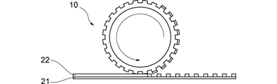
本実施形態の版胴をローラーモールドとして使用する場合には、版胴10を、基材21上のインク22に接触させる。これにより、基材21上のインク22に、版胴の外周面に形成されたパターンを転写(型押し)することができる(図5参照)。本実施形態の版胴は、パターンを形成することができる円筒版1の厚さが厚いため、従来のローラーモールドと比較してより深いパターンを形成することが可能となる。
[Roller mold]
When the plate cylinder of the present embodiment is used as a roller mold, the
なお、インク22に含まれる成分としては、特に限定されないが、例えば、金属粒子、溶剤、及び界面活性剤が挙げられる。溶剤及び界面活性剤は、金属粒子を分散可能であり、かつ焼結の際に残留しにくいよう構成されていれば特に制限されない。
The components contained in the
〔反転印刷〕
本実施形態の版胴を反転印刷の版胴として使用する場合には、版胴10を、基材21(ブランケット)上のインク22に接触させる。これにより、基材21上に、版胴の外周面に形成されたパターンを転写することができる。基材21上にパターンを形成後、形成されたパターンを、被印刷物上に転写する(図6参照)。本実施形態の版胴は、パターンを形成することができる円筒版1の厚さが厚いため、より深いパターンを形成することが可能となる。より深いパターンを形成することで、表面積及びパターンの断面積が増大するため、抵抗値が低下する傾向にある。
[Reverse printing]
When the plate cylinder of the present embodiment is used as a plate cylinder for reverse printing, the
〔版胴の製造方法〕
本実施形態の版胴の製造方法は、シリコンインゴットを中抜きして厚さが5μm以上である円筒状のシリコン(円筒版1)を得る中抜き工程と、該中抜き工程により得られた前記シリコンの円筒内に芯金2を嵌合する嵌合工程Aと、を有する。図7に、本実施形態の版胴の製造方法の工程に沿って円筒版と芯金との関係を表すチャートを例示する。
[Manufacturing method of plate cylinder]
The method for manufacturing a plate cylinder of the present embodiment includes a hollowing step of punching a silicon ingot to obtain cylindrical silicon (cylindrical plate 1) having a thickness of 5 μm or more, and the hollowing step obtained by the hollowing step. It has a fitting step A for fitting the
〔接着層形成工程〕
別の態様として、版胴の製造方法は、嵌合工程の前に、中抜き工程により得られた円筒版1の内面側、又は、芯金2の外面側に、接着層3となる低融点金属を塗布する工程と、嵌合工程の後に、低融点金属を溶融させて接着層3を形成する工程Bと、を有していてもよい。
[Adhesive layer forming process]
As another aspect, in the method of manufacturing the plate cylinder, before the fitting process, the low melting point of the
〔研削/研磨工程〕
また別の態様として、本実施形態の版胴の製造方法は、中抜き工程の前又は中抜き工程の後のシリコンインゴットの外周面を研削又は研磨する工程、及び/又は、芯金2に嵌合した後の円筒版1の外周面を研削又は研磨する工程Cを有していてもよい。
[Grinding / polishing process]
As another aspect, the method for manufacturing the plate cylinder of the present embodiment is a step of grinding or polishing the outer peripheral surface of the silicon ingot before or after the hollowing step, and / or fitting it into the
〔パターン形成工程〕
さらに、本実施形態の版胴の製造方法は、円筒版1の外周面にパターンを形成するパターン形成工程Dを有していてもよい。パターン形成方法としては、特に限定されないが、例えば、電子ビーム露光により描画する方法、シリコンである円筒版1の表面にエッチングマスクを形成し、シリコン表面をエッチングする方法等が挙げられる。
[Pattern formation process]
Further, the plate cylinder manufacturing method of the present embodiment may include a pattern forming step D for forming a pattern on the outer peripheral surface of the
本発明の版胴は、各種印刷用途において、産業上の利用可能性を有する。 The plate cylinder of the present invention has industrial applicability in various printing applications.
1…円筒版
2…芯金
3…接着層
10…版胴
21…基材
22…インク
1 ...
Claims (4)
該円筒版の回転軸を有する芯金と、
融点が600℃以下の金属を含み、前記芯金と前記円筒版とを接着する導電性の接着層と、を備え、
前記円筒版と前記回転軸との間に導電性を有する、
版胴。 Thickness Ri Tona cylindrical silicon is 5μm or more, the cylindrical plate that have a pattern formed by grooves on the outer peripheral surface,
A core metal having a rotating shaft of the cylindrical plate and
A conductive adhesive layer containing a metal having a melting point of 600 ° C. or lower and adhering the core metal and the cylindrical plate is provided.
Conductive between the cylindrical plate and the rotating shaft .
Plate body.
請求項1に記載の版胴。 The core metal has a flow path for passing a refrigerant.
The plate cylinder according to claim 1.
請求項1又は2に記載の版胴。 The silicon is single crystal silicon.
The plate cylinder according to claim 1 or 2.
該中抜き工程により得られた前記シリコンの内面側、及び、芯金の外面側、の少なくともいずれか一方に融点が600℃以下の金属を含む導電性の接着層を塗布する接着層形成工程と、
前記シリコンの円筒内に前記芯金を嵌合する嵌合工程と、
前記芯金をアースに電気的に接続し、電子ビーム露光によって、前記円筒状のシリコンの外周面にパターンを描画するパターン形成工程と、を有する、
版胴の製造方法。 A hollowing process to obtain cylindrical silicon with a thickness of 5 μm or more by hollowing out a silicon ingot, and
An adhesive layer forming step of applying a conductive adhesive layer containing a metal having a melting point of 600 ° C. or less to at least one of the inner surface side of the silicon and the outer surface side of the core metal obtained by the hollowing step. ,
A fitting step of fitting the core metal into the cylinder of the silicon,
It has a pattern forming step of electrically connecting the core metal to the ground and drawing a pattern on the outer peripheral surface of the cylindrical silicon by electron beam exposure .
How to manufacture the plate cylinder.
Priority Applications (1)
| Application Number | Priority Date | Filing Date | Title |
|---|---|---|---|
| JP2016247646A JP6906944B2 (en) | 2016-12-21 | 2016-12-21 | Plate cylinder and its manufacturing method |
Applications Claiming Priority (1)
| Application Number | Priority Date | Filing Date | Title |
|---|---|---|---|
| JP2016247646A JP6906944B2 (en) | 2016-12-21 | 2016-12-21 | Plate cylinder and its manufacturing method |
Publications (2)
| Publication Number | Publication Date |
|---|---|
| JP2018101715A JP2018101715A (en) | 2018-06-28 |
| JP6906944B2 true JP6906944B2 (en) | 2021-07-21 |
Family
ID=62714474
Family Applications (1)
| Application Number | Title | Priority Date | Filing Date |
|---|---|---|---|
| JP2016247646A Active JP6906944B2 (en) | 2016-12-21 | 2016-12-21 | Plate cylinder and its manufacturing method |
Country Status (1)
| Country | Link |
|---|---|
| JP (1) | JP6906944B2 (en) |
Family Cites Families (4)
| Publication number | Priority date | Publication date | Assignee | Title |
|---|---|---|---|---|
| JPH0470891A (en) * | 1990-07-12 | 1992-03-05 | Toppan Printing Co Ltd | Production of cooling roll and diffraction grating sheet |
| JP4957139B2 (en) * | 2006-09-20 | 2012-06-20 | 大日本印刷株式会社 | Mold manufacturing method |
| KR101371996B1 (en) * | 2009-06-05 | 2014-03-07 | 아사히 가세이 이-매터리얼즈 가부시키가이샤 | Method of manufacturing transfer mold and transfer mold |
| JP6208924B2 (en) * | 2011-10-19 | 2017-10-04 | 旭化成株式会社 | Microstructure transfer mold, method for manufacturing microstructure transfer mold, and method for manufacturing surface microstructure member |
-
2016
- 2016-12-21 JP JP2016247646A patent/JP6906944B2/en active Active
Also Published As
| Publication number | Publication date |
|---|---|
| JP2018101715A (en) | 2018-06-28 |
Similar Documents
| Publication | Publication Date | Title |
|---|---|---|
| EP3556899B1 (en) | Vapor deposition mask device and method for manufacturing vapor deposition mask device | |
| KR102109071B1 (en) | Film forming mask | |
| KR101786391B1 (en) | Alloy metal foil for deposition mask, deposition mask using the alloy metal foil and method for preparing them, and method for preparing organic electroluminescent device | |
| JP2007015235A (en) | Image forming method, and image forming device using it | |
| TW201825714A (en) | Mask manufacturing method and mother board used for the mask | |
| JP6906944B2 (en) | Plate cylinder and its manufacturing method | |
| JP2017164979A (en) | Printing plate | |
| US20080217819A1 (en) | Micro/Nano-Pattern Film Contact Transfer Process | |
| US8998385B2 (en) | Thermal head, printer, and method of manufacturing thermal head | |
| CN104988458A (en) | Manufacturing method for mask plate with taper-angled opening | |
| KR20200137591A (en) | Mask metal sheet for producing mask | |
| JP5273786B2 (en) | Thermal head, printer, and thermal head manufacturing method | |
| JP2005158295A (en) | Electrode-forming ink for plasma display panel and manufacturing method for electrode substrate for plasma display panel using it | |
| JP2013006302A (en) | Roll-shaped stamper, and method for manufacturing the same | |
| JPH06251714A (en) | Display panel and manufacture thereof | |
| KR20120087675A (en) | High Definition Printing Plate of Liquid Crystal Display and Method for Manufacture using the same | |
| JP6757693B2 (en) | Manufacturing method of sample loading plate | |
| JP2006028604A (en) | Method for transferring minute shape, method for manufacturing casting mold, surface treatment method for casting mold, and casting mold | |
| CN118547240B (en) | Mask plate preparation method and mask plate | |
| JP2007046106A (en) | Boat for vapor deposition, and vacuum deposition system provided therewith | |
| JP2019065364A (en) | Sputtering target and sputtering apparatus | |
| JP4612852B2 (en) | Imprint master, imprint apparatus including the imprint master, and method for manufacturing the imprint master | |
| JP2005277525A (en) | Antenna and its manufacturing method | |
| JP5948583B2 (en) | Ultraviolet curable conductive ink, manufacturing method thereof, and circuit manufacturing method | |
| KR20190004478A (en) | Producing method of mask |
Legal Events
| Date | Code | Title | Description |
|---|---|---|---|
| A621 | Written request for application examination |
Free format text: JAPANESE INTERMEDIATE CODE: A621 Effective date: 20191206 |
|
| A977 | Report on retrieval |
Free format text: JAPANESE INTERMEDIATE CODE: A971007 Effective date: 20201225 |
|
| A131 | Notification of reasons for refusal |
Free format text: JAPANESE INTERMEDIATE CODE: A131 Effective date: 20210107 |
|
| A521 | Written amendment |
Free format text: JAPANESE INTERMEDIATE CODE: A523 Effective date: 20210304 |
|
| TRDD | Decision of grant or rejection written | ||
| A01 | Written decision to grant a patent or to grant a registration (utility model) |
Free format text: JAPANESE INTERMEDIATE CODE: A01 Effective date: 20210618 |
|
| A61 | First payment of annual fees (during grant procedure) |
Free format text: JAPANESE INTERMEDIATE CODE: A61 Effective date: 20210630 |
|
| R150 | Certificate of patent or registration of utility model |
Ref document number: 6906944 Country of ref document: JP Free format text: JAPANESE INTERMEDIATE CODE: R150 |