JP6729670B2 - 表示ドライバー、電気光学装置及び電子機器 - Google Patents
表示ドライバー、電気光学装置及び電子機器 Download PDFInfo
- Publication number
- JP6729670B2 JP6729670B2 JP2018231291A JP2018231291A JP6729670B2 JP 6729670 B2 JP6729670 B2 JP 6729670B2 JP 2018231291 A JP2018231291 A JP 2018231291A JP 2018231291 A JP2018231291 A JP 2018231291A JP 6729670 B2 JP6729670 B2 JP 6729670B2
- Authority
- JP
- Japan
- Prior art keywords
- circuit
- node
- calibration
- resistance
- display driver
- Prior art date
- Legal status (The legal status is an assumption and is not a legal conclusion. Google has not performed a legal analysis and makes no representation as to the accuracy of the status listed.)
- Active
Links
Images


Classifications
-
- G—PHYSICS
- G09—EDUCATION; CRYPTOGRAPHY; DISPLAY; ADVERTISING; SEALS
- G09G—ARRANGEMENTS OR CIRCUITS FOR CONTROL OF INDICATING DEVICES USING STATIC MEANS TO PRESENT VARIABLE INFORMATION
- G09G3/00—Control arrangements or circuits, of interest only in connection with visual indicators other than cathode-ray tubes
- G09G3/20—Control arrangements or circuits, of interest only in connection with visual indicators other than cathode-ray tubes for presentation of an assembly of a number of characters, e.g. a page, by composing the assembly by combination of individual elements arranged in a matrix no fixed position being assigned to or needed to be assigned to the individual characters or partial characters
- G09G3/34—Control arrangements or circuits, of interest only in connection with visual indicators other than cathode-ray tubes for presentation of an assembly of a number of characters, e.g. a page, by composing the assembly by combination of individual elements arranged in a matrix no fixed position being assigned to or needed to be assigned to the individual characters or partial characters by control of light from an independent source
- G09G3/36—Control arrangements or circuits, of interest only in connection with visual indicators other than cathode-ray tubes for presentation of an assembly of a number of characters, e.g. a page, by composing the assembly by combination of individual elements arranged in a matrix no fixed position being assigned to or needed to be assigned to the individual characters or partial characters by control of light from an independent source using liquid crystals
- G09G3/3611—Control of matrices with row and column drivers
- G09G3/3685—Details of drivers for data electrodes
- G09G3/3688—Details of drivers for data electrodes suitable for active matrices only
-
- G—PHYSICS
- G09—EDUCATION; CRYPTOGRAPHY; DISPLAY; ADVERTISING; SEALS
- G09G—ARRANGEMENTS OR CIRCUITS FOR CONTROL OF INDICATING DEVICES USING STATIC MEANS TO PRESENT VARIABLE INFORMATION
- G09G3/00—Control arrangements or circuits, of interest only in connection with visual indicators other than cathode-ray tubes
- G09G3/20—Control arrangements or circuits, of interest only in connection with visual indicators other than cathode-ray tubes for presentation of an assembly of a number of characters, e.g. a page, by composing the assembly by combination of individual elements arranged in a matrix no fixed position being assigned to or needed to be assigned to the individual characters or partial characters
- G09G3/34—Control arrangements or circuits, of interest only in connection with visual indicators other than cathode-ray tubes for presentation of an assembly of a number of characters, e.g. a page, by composing the assembly by combination of individual elements arranged in a matrix no fixed position being assigned to or needed to be assigned to the individual characters or partial characters by control of light from an independent source
- G09G3/36—Control arrangements or circuits, of interest only in connection with visual indicators other than cathode-ray tubes for presentation of an assembly of a number of characters, e.g. a page, by composing the assembly by combination of individual elements arranged in a matrix no fixed position being assigned to or needed to be assigned to the individual characters or partial characters by control of light from an independent source using liquid crystals
- G09G3/3611—Control of matrices with row and column drivers
- G09G3/3685—Details of drivers for data electrodes
-
- H—ELECTRICITY
- H03—ELECTRONIC CIRCUITRY
- H03F—AMPLIFIERS
- H03F1/00—Details of amplifiers with only discharge tubes, only semiconductor devices or only unspecified devices as amplifying elements
- H03F1/34—Negative-feedback-circuit arrangements with or without positive feedback
-
- H—ELECTRICITY
- H03—ELECTRONIC CIRCUITRY
- H03F—AMPLIFIERS
- H03F3/00—Amplifiers with only discharge tubes or only semiconductor devices as amplifying elements
- H03F3/45—Differential amplifiers
- H03F3/45071—Differential amplifiers with semiconductor devices only
-
- H—ELECTRICITY
- H03—ELECTRONIC CIRCUITRY
- H03F—AMPLIFIERS
- H03F3/00—Amplifiers with only discharge tubes or only semiconductor devices as amplifying elements
- H03F3/45—Differential amplifiers
- H03F3/45071—Differential amplifiers with semiconductor devices only
- H03F3/45076—Differential amplifiers with semiconductor devices only characterised by the way of implementation of the active amplifying circuit in the differential amplifier
- H03F3/45475—Differential amplifiers with semiconductor devices only characterised by the way of implementation of the active amplifying circuit in the differential amplifier using IC blocks as the active amplifying circuit
-
- H—ELECTRICITY
- H03—ELECTRONIC CIRCUITRY
- H03M—CODING; DECODING; CODE CONVERSION IN GENERAL
- H03M1/00—Analogue/digital conversion; Digital/analogue conversion
- H03M1/66—Digital/analogue converters
- H03M1/74—Simultaneous conversion
- H03M1/80—Simultaneous conversion using weighted impedances
- H03M1/808—Simultaneous conversion using weighted impedances using resistors
-
- G—PHYSICS
- G09—EDUCATION; CRYPTOGRAPHY; DISPLAY; ADVERTISING; SEALS
- G09G—ARRANGEMENTS OR CIRCUITS FOR CONTROL OF INDICATING DEVICES USING STATIC MEANS TO PRESENT VARIABLE INFORMATION
- G09G2310/00—Command of the display device
- G09G2310/02—Addressing, scanning or driving the display screen or processing steps related thereto
- G09G2310/0264—Details of driving circuits
- G09G2310/027—Details of drivers for data electrodes, the drivers handling digital grey scale data, e.g. use of D/A converters
-
- G—PHYSICS
- G09—EDUCATION; CRYPTOGRAPHY; DISPLAY; ADVERTISING; SEALS
- G09G—ARRANGEMENTS OR CIRCUITS FOR CONTROL OF INDICATING DEVICES USING STATIC MEANS TO PRESENT VARIABLE INFORMATION
- G09G2310/00—Command of the display device
- G09G2310/02—Addressing, scanning or driving the display screen or processing steps related thereto
- G09G2310/0264—Details of driving circuits
- G09G2310/0291—Details of output amplifiers or buffers arranged for use in a driving circuit
-
- G—PHYSICS
- G09—EDUCATION; CRYPTOGRAPHY; DISPLAY; ADVERTISING; SEALS
- G09G—ARRANGEMENTS OR CIRCUITS FOR CONTROL OF INDICATING DEVICES USING STATIC MEANS TO PRESENT VARIABLE INFORMATION
- G09G2320/00—Control of display operating conditions
- G09G2320/06—Adjustment of display parameters
- G09G2320/0693—Calibration of display systems
-
- G—PHYSICS
- G09—EDUCATION; CRYPTOGRAPHY; DISPLAY; ADVERTISING; SEALS
- G09G—ARRANGEMENTS OR CIRCUITS FOR CONTROL OF INDICATING DEVICES USING STATIC MEANS TO PRESENT VARIABLE INFORMATION
- G09G3/00—Control arrangements or circuits, of interest only in connection with visual indicators other than cathode-ray tubes
- G09G3/20—Control arrangements or circuits, of interest only in connection with visual indicators other than cathode-ray tubes for presentation of an assembly of a number of characters, e.g. a page, by composing the assembly by combination of individual elements arranged in a matrix no fixed position being assigned to or needed to be assigned to the individual characters or partial characters
- G09G3/34—Control arrangements or circuits, of interest only in connection with visual indicators other than cathode-ray tubes for presentation of an assembly of a number of characters, e.g. a page, by composing the assembly by combination of individual elements arranged in a matrix no fixed position being assigned to or needed to be assigned to the individual characters or partial characters by control of light from an independent source
- G09G3/36—Control arrangements or circuits, of interest only in connection with visual indicators other than cathode-ray tubes for presentation of an assembly of a number of characters, e.g. a page, by composing the assembly by combination of individual elements arranged in a matrix no fixed position being assigned to or needed to be assigned to the individual characters or partial characters by control of light from an independent source using liquid crystals
- G09G3/3611—Control of matrices with row and column drivers
- G09G3/3614—Control of polarity reversal in general
-
- H—ELECTRICITY
- H03—ELECTRONIC CIRCUITRY
- H03F—AMPLIFIERS
- H03F2203/00—Indexing scheme relating to amplifiers with only discharge tubes or only semiconductor devices as amplifying elements covered by H03F3/00
- H03F2203/45—Indexing scheme relating to differential amplifiers
- H03F2203/45151—At least one resistor being added at the input of a dif amp
-
- H—ELECTRICITY
- H03—ELECTRONIC CIRCUITRY
- H03F—AMPLIFIERS
- H03F2203/00—Indexing scheme relating to amplifiers with only discharge tubes or only semiconductor devices as amplifying elements covered by H03F3/00
- H03F2203/45—Indexing scheme relating to differential amplifiers
- H03F2203/45336—Indexing scheme relating to differential amplifiers the AAC comprising one or more resistors as feedback circuit elements
-
- H—ELECTRICITY
- H03—ELECTRONIC CIRCUITRY
- H03F—AMPLIFIERS
- H03F2203/00—Indexing scheme relating to amplifiers with only discharge tubes or only semiconductor devices as amplifying elements covered by H03F3/00
- H03F2203/45—Indexing scheme relating to differential amplifiers
- H03F2203/45522—Indexing scheme relating to differential amplifiers the FBC comprising one or more potentiometers
-
- H—ELECTRICITY
- H03—ELECTRONIC CIRCUITRY
- H03F—AMPLIFIERS
- H03F2203/00—Indexing scheme relating to amplifiers with only discharge tubes or only semiconductor devices as amplifying elements covered by H03F3/00
- H03F2203/45—Indexing scheme relating to differential amplifiers
- H03F2203/45591—Indexing scheme relating to differential amplifiers the IC comprising one or more potentiometers
-
- H—ELECTRICITY
- H03—ELECTRONIC CIRCUITRY
- H03M—CODING; DECODING; CODE CONVERSION IN GENERAL
- H03M1/00—Analogue/digital conversion; Digital/analogue conversion
- H03M1/66—Digital/analogue converters
- H03M1/74—Simultaneous conversion
- H03M1/76—Simultaneous conversion using switching tree
- H03M1/765—Simultaneous conversion using switching tree using a single level of switches which are controlled by unary decoded digital signals
Landscapes
- Engineering & Computer Science (AREA)
- Theoretical Computer Science (AREA)
- Power Engineering (AREA)
- Chemical & Material Sciences (AREA)
- Crystallography & Structural Chemistry (AREA)
- Physics & Mathematics (AREA)
- Computer Hardware Design (AREA)
- General Physics & Mathematics (AREA)
- Liquid Crystal Display Device Control (AREA)
- Control Of Indicators Other Than Cathode Ray Tubes (AREA)
- Analogue/Digital Conversion (AREA)
- Liquid Crystal (AREA)
Description
図1は、表示ドライバー100の構成例である。図1の表示ドライバー100は、電気光学パネルの画素にデータ電圧を供給することで、電気光学パネルを駆動するものである。電気光学パネルとして、例えばアクティブマトリックス型の液晶表示パネル、或いはEL(Electro Luminescence)表示パネルを想定できる。表示ドライバー100は集積回路装置である。
図3に、第1実施形態におけるアンプ回路AM1の構成例を示す。また図3には、階調電圧生成回路50の詳細な構成例を示す。以下ではアンプ回路AM1を例に説明するが、アンプ回路AM2〜AMtも同様な構成である。また以下では表示データDT1が7ビットである場合を例に説明するが、表示データのビット数は任意である。
図4に、第2実施形態におけるアンプ回路AM1の構成例を示す。以下ではアンプ回路AM1を例に説明するが、アンプ回路AM2〜AMtも同様な構成である。なお既に説明した構成要素には同一の符号を付し、その構成要素の説明を適宜に省略する。
図5に、第3実施形態におけるアンプ回路AM1の構成例を示す。以下ではアンプ回路AM1を例に説明するが、アンプ回路AM2〜AMtも同様な構成である。なお既に説明した構成要素には同一の符号を付し、その構成要素の説明を適宜に省略する。
図6に、第4実施形態における表示ドライバー100及びアンプ回路AM1の構成例を示す。以下ではアンプ回路AM1に関する構成を例に説明するが、アンプ回路AM2〜AMtに関する構成も同様な構成である。なお既に説明した構成要素には同一の符号を付し、その構成要素の説明を適宜に省略する。
図7は、キャリブレーションを行う場合の表示ドライバー100及びアンプ回路AM1の構成例である。以下ではアンプ回路AM1に関する構成を例に説明するが、アンプ回路AM2〜AMtに関する構成も同様な構成である。また図7では階調電圧生成回路50の図示を省略している。なお既に説明した構成要素には同一の符号を付し、その構成要素の説明を適宜に省略する。
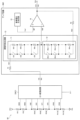
図11は、表示ドライバー100を含む電気光学装置350の構成例である。電気光学装置350は、表示ドライバー100、電気光学パネル200を含む。
Claims (17)
- 表示データを階調電圧に変換するD/A変換回路と、
入力ノードに前記階調電圧が入力され、データ電圧を出力するアンプ回路と、
を含み、
前記アンプ回路は、
非反転入力ノードに基準電圧が入力される演算増幅器と、
前記入力ノードと、第1ノードとの間に設けられる第1抵抗と、
第2ノードと、前記演算増幅器の出力ノードとの間に設けられる第2抵抗と、
前記第1ノードと前記演算増幅器の反転入力ノードとの間の抵抗値である第1調整用抵抗値、及び前記第2ノードと前記演算増幅器の前記反転入力ノードとの間の抵抗値である第2調整用抵抗値を、調整する調整用抵抗回路と、
を有することを特徴とする表示ドライバー。 - 請求項1に記載の表示ドライバーにおいて、
前記調整用抵抗回路は、
前記第1ノードと前記演算増幅器の前記反転入力ノードとの間に設けられ、前記第1調整用抵抗値を可変に設定する第1抵抗回路と、
前記第2ノードと前記演算増幅器の前記反転入力ノードとの間に設けられ、前記第2調整用抵抗値を可変に設定する第2抵抗回路と、
を有することを特徴とする表示ドライバー。 - 請求項2に記載の表示ドライバーにおいて、
前記第1抵抗回路は、
前記第1ノードと前記演算増幅器の前記反転入力ノードとの間に直列に接続される第1〜第n抵抗素子(nは2以上の整数)と、
第iスイッチ素子(iは1以上n以下の整数)が、前記第1〜第n抵抗素子の第i抵抗素子に対して並列に設けられる第1〜第nスイッチ素子と、
を有し、
第2抵抗回路は、
前記第2ノードと前記演算増幅器の前記反転入力ノードとの間に直列に接続される第n+1〜第mの抵抗素子(mはn+2以上の整数)と、
第jスイッチ素子(jはn+1以上m以下の整数)が、第n+1〜第m抵抗素子の第j抵抗素子に対して並列に設けられる第n+1〜第mスイッチ素子と、
を有することを特徴とする表示ドライバー。 - 請求項1に記載の表示ドライバーにおいて、
前記調整用抵抗回路は、
前記第1ノードと前記第2ノードとの間に設けられたラダー抵抗回路と、
前記ラダー抵抗回路の複数のタップのいずれかを前記演算増幅器の前記反転入力ノードに接続するセレクターと、
を有することを特徴とする表示ドライバー。 - 請求項1乃至4のいずれか一項に記載の表示ドライバーにおいて、
前記第1調整用抵抗値及び前記第2調整用抵抗値をキャリブレーションすることで、前記アンプ回路のゲインキャリブレーションを行うキャリブレーション回路を含むことを特徴とする表示ドライバー。 - 請求項5に記載の表示ドライバーにおいて、
前記キャリブレーション回路は、
前記アンプ回路の出力が階調のセンター電圧となるように、前記演算増幅器の前記非反転入力ノードに入力される前記基準電圧を調整することで、前記アンプ回路のオフセットキャリブレーションを行い、
前記入力ノードに所定電圧を入力した状態で、前記第1調整用抵抗値及び前記第2調整用抵抗値を調整することで、前記ゲインキャリブレーションを行うことを特徴とする表示ドライバー。 - 請求項6に記載の表示ドライバーにおいて、
前記キャリブレーション回路は、
前記入力ノードがハイインピーダンスとなった状態で、前記アンプ回路の出力が前記センター電圧となるように前記基準電圧を調整することで、前記オフセットキャリブレーションを行うことを特徴とする表示ドライバー。 - 請求項5乃至7のいずれか一項に記載の表示ドライバーにおいて、
前記キャリブレーション回路は、
正極性駆動用の前記第1調整用抵抗値及び前記第2調整用抵抗値を決定する正極性ゲインキャリブレーションと、負極性駆動用の前記第1調整用抵抗値及び前記第2調整用抵抗値を決定する負極性ゲインキャリブレーションと、を行うことを特徴とする表示ドライバー。 - 請求項5乃至8のいずれか一項に記載の表示ドライバーにおいて、
第2表示データを第2階調電圧に変換する第2D/A変換回路と、
第2入力ノードに前記第2階調電圧が入力され、第2データ電圧を出力する第2アンプ回路と、
を含み、
前記第2アンプ回路は、
第2非反転入力ノードに第2基準電圧が入力される第2演算増幅器と、
前記第2入力ノードと、第3ノードとの間に設けられる第3抵抗と、
第4ノードと、前記第2演算増幅器の第2出力ノードとの間に設けられる第4抵抗と、
前記第3ノードと前記第2演算増幅器の第2反転入力ノードとの間の第3調整用抵抗値、及び前記第4ノードと前記第2演算増幅器の前記第2反転入力ノードとの間の第4調整用抵抗値を、調整する第2調整用抵抗回路と、
を有し、
前記キャリブレーション回路は、前記アンプ回路と前記第2アンプ回路が同一ゲインとなるように前記ゲインキャリブレーションを行うことを特徴とする表示ドライバー。 - 表示データを階調電圧に変換するD/A変換回路と、
入力ノードに前記階調電圧が入力され、データ電圧を出力するアンプ回路と、
を含み、
前記アンプ回路は、
非反転入力ノードに基準電圧が入力される演算増幅器と、
第1ノードと前記演算増幅器の反転入力ノードとの間に設けられる第1抵抗と、
前記演算増幅器の前記反転入力ノードと前記演算増幅器の出力ノードとの間に設けられる第2抵抗と、
前記入力ノードと前記第1ノードとの間に設けられ、前記入力ノードと前記第1ノードとの間の抵抗値を調整する調整用抵抗回路と、
を含むことを特徴とする表示ドライバー。 - 請求項10に記載の表示ドライバーにおいて、
前記調整用抵抗回路の前記抵抗値をキャリブレーションすることで、前記アンプ回路のゲインキャリブレーションを行うキャリブレーション回路を含むことを特徴とする表示ドライバー。 - 請求項11に記載の表示ドライバーにおいて、
前記キャリブレーション回路は、
正極性駆動における前記調整用抵抗回路の前記抵抗値を決定する正極性ゲインキャリブレーションと、負極性駆動における前記調整用抵抗回路の前記抵抗値を決定する負極性ゲインキャリブレーションと、を行うことを特徴とする表示ドライバー。 - 表示データに対して演算処理する演算回路と、
前記演算回路の出力データを階調電圧に変換するD/A変換回路と、
入力ノードに前記階調電圧が入力され、データ電圧を出力するアンプ回路と、
を含み、
前記アンプ回路は、
非反転入力ノードに基準電圧が入力される演算増幅器と、
前記入力ノードと前記演算増幅器の反転入力ノードとの間に設けられる第1抵抗と、
前記演算増幅器の前記反転入力ノードと前記演算増幅器の出力ノードとの間に設けられる第2抵抗と、
を有し、
前記演算回路は、
前記第1抵抗と前記第2抵抗の比を補正する前記演算処理を前記表示データに対して行うことで、前記出力データを出力することを特徴とする表示ドライバー。 - 請求項13に記載の表示ドライバーにおいて、
前記第1抵抗と前記第2抵抗の前記比がキャリブレーションされるように前記演算処理を決定することで、前記アンプ回路のゲインキャリブレーションを行うキャリブレーション回路を含むことを特徴とする表示ドライバー。 - 請求項14に記載の表示ドライバーにおいて、
前記キャリブレーション回路は、
正極性駆動における前記演算処理を決定する正極性ゲインキャリブレーションと、負極性駆動における前記演算処理を決定する負極性ゲインキャリブレーションと、を行うことを特徴とする表示ドライバー。 - 電気光学パネルと、
請求項1乃至15のいずれか一項に記載され、前記電気光学パネルを駆動する表示ドライバーと、
を含むことを特徴とする電気光学装置。 - 請求項1乃至15のいずれか一項に記載の表示ドライバーを含むことを特徴とする電子機器。
Priority Applications (2)
| Application Number | Priority Date | Filing Date | Title |
|---|---|---|---|
| JP2018231291A JP6729670B2 (ja) | 2018-12-11 | 2018-12-11 | 表示ドライバー、電気光学装置及び電子機器 |
| US16/708,535 US10937382B2 (en) | 2018-12-11 | 2019-12-10 | Display driver, electro-optical device, and electronic apparatus |
Applications Claiming Priority (1)
| Application Number | Priority Date | Filing Date | Title |
|---|---|---|---|
| JP2018231291A JP6729670B2 (ja) | 2018-12-11 | 2018-12-11 | 表示ドライバー、電気光学装置及び電子機器 |
Publications (2)
| Publication Number | Publication Date |
|---|---|
| JP2020095100A JP2020095100A (ja) | 2020-06-18 |
| JP6729670B2 true JP6729670B2 (ja) | 2020-07-22 |
Family
ID=70971831
Family Applications (1)
| Application Number | Title | Priority Date | Filing Date |
|---|---|---|---|
| JP2018231291A Active JP6729670B2 (ja) | 2018-12-11 | 2018-12-11 | 表示ドライバー、電気光学装置及び電子機器 |
Country Status (2)
| Country | Link |
|---|---|
| US (1) | US10937382B2 (ja) |
| JP (1) | JP6729670B2 (ja) |
Families Citing this family (2)
| Publication number | Priority date | Publication date | Assignee | Title |
|---|---|---|---|---|
| US11012079B1 (en) * | 2019-12-19 | 2021-05-18 | Bae Systems Information And Electronic Systems Integration Inc. | Continuous tuning of digitally switched voltage-controlled oscillator frequency bands |
| JP2023034746A (ja) * | 2021-08-31 | 2023-03-13 | セイコーエプソン株式会社 | 表示ドライバー及び表示モジュール |
Family Cites Families (23)
| Publication number | Priority date | Publication date | Assignee | Title |
|---|---|---|---|---|
| US5739805A (en) * | 1994-12-15 | 1998-04-14 | David Sarnoff Research Center, Inc. | Matrix addressed LCD display having LCD age indication, and autocalibrated amplification driver, and a cascaded column driver with capacitor-DAC operating on split groups of data bits |
| JP3367808B2 (ja) * | 1995-06-19 | 2003-01-20 | シャープ株式会社 | 表示パネルの駆動方法および装置 |
| JP3780531B2 (ja) | 1997-06-30 | 2006-05-31 | セイコーエプソン株式会社 | 映像信号処理回路、それを用いた映像表示装置及び電子機器並びにディジタル−アナログ変換器の出力調整方法 |
| JPH11175027A (ja) * | 1997-12-08 | 1999-07-02 | Hitachi Ltd | 液晶駆動回路および液晶表示装置 |
| JP3813463B2 (ja) * | 2000-07-24 | 2006-08-23 | シャープ株式会社 | 液晶表示装置の駆動回路及びそれを用いた液晶表示装置並びにその液晶表示装置を用いた電子機器 |
| JP4766760B2 (ja) * | 2001-03-06 | 2011-09-07 | ルネサスエレクトロニクス株式会社 | 液晶駆動装置 |
| JP3661651B2 (ja) * | 2002-02-08 | 2005-06-15 | セイコーエプソン株式会社 | 基準電圧発生回路、表示駆動回路及び表示装置 |
| TWI235988B (en) * | 2004-03-29 | 2005-07-11 | Novatek Microelectronics Corp | Driving circuit of liquid crystal display |
| TW200601259A (en) * | 2004-06-28 | 2006-01-01 | Rohm Co Ltd | Color display device and semiconductor device for the same |
| KR100674924B1 (ko) * | 2004-12-03 | 2007-01-26 | 삼성전자주식회사 | 커패시터 dac를 이용하여 비선형 감마 특성을 구현하는감마 보정 장치 및 그 감마 보정 방법 |
| US10013907B2 (en) * | 2004-12-15 | 2018-07-03 | Ignis Innovation Inc. | Method and system for programming, calibrating and/or compensating, and driving an LED display |
| JP2006227272A (ja) * | 2005-02-17 | 2006-08-31 | Seiko Epson Corp | 基準電圧発生回路、表示ドライバ、電気光学装置及び電子機器 |
| JP4442455B2 (ja) * | 2005-02-17 | 2010-03-31 | セイコーエプソン株式会社 | 基準電圧選択回路、基準電圧発生回路、表示ドライバ、電気光学装置及び電子機器 |
| JP4645258B2 (ja) * | 2005-03-25 | 2011-03-09 | 日本電気株式会社 | デジタルアナログ変換回路及び表示装置 |
| US7280063B2 (en) * | 2005-04-29 | 2007-10-09 | Georgia Tech Research Corporation | Programmable voltage-output floating-gate digital to analog converter and tunable resistors |
| KR100770723B1 (ko) * | 2006-03-16 | 2007-10-30 | 삼성전자주식회사 | 평판 표시 장치의 소스 드라이버의 디지털/아날로그변환장치 및 디지털/아날로그 변환방법. |
| JP2007279186A (ja) | 2006-04-04 | 2007-10-25 | Nec Electronics Corp | 増幅回路、及び駆動回路 |
| US8242944B2 (en) * | 2007-04-26 | 2012-08-14 | Renesas Electronics Corporation | Digital-to-analog converter circuit including adder drive circuit and display |
| JP2010044686A (ja) * | 2008-08-18 | 2010-02-25 | Oki Semiconductor Co Ltd | バイアス電圧生成回路及びドライバ集積回路 |
| KR101534150B1 (ko) * | 2009-02-13 | 2015-07-07 | 삼성전자주식회사 | 하이브리드 디지털/아날로그 컨버터, 소스 드라이버 및 액정 표시 장치 |
| CN104021771B (zh) * | 2014-06-17 | 2017-02-15 | 深圳市华星光电技术有限公司 | 一种可编程伽玛校正缓冲电路芯片及产生伽马电压的方法 |
| KR102320300B1 (ko) * | 2014-12-01 | 2021-11-03 | 삼성디스플레이 주식회사 | 유기 발광 표시 장치 |
| JP6540043B2 (ja) | 2015-01-27 | 2019-07-10 | セイコーエプソン株式会社 | ドライバー、電気光学装置及び電子機器 |
-
2018
- 2018-12-11 JP JP2018231291A patent/JP6729670B2/ja active Active
-
2019
- 2019-12-10 US US16/708,535 patent/US10937382B2/en active Active
Also Published As
| Publication number | Publication date |
|---|---|
| US10937382B2 (en) | 2021-03-02 |
| US20200184916A1 (en) | 2020-06-11 |
| JP2020095100A (ja) | 2020-06-18 |
Similar Documents
| Publication | Publication Date | Title |
|---|---|---|
| JP4193771B2 (ja) | 階調電圧発生回路及び駆動回路 | |
| US10878767B2 (en) | Display driver, electro-optical device, and electronic apparatus | |
| US10573219B2 (en) | Display driver, electro-optical device, and electronic apparatus | |
| JP6058289B2 (ja) | 表示装置、撮像装置及び階調電圧生成回路 | |
| JP4779167B2 (ja) | 液晶表示装置の駆動方法、オーバードライブ補正装置、オーバードライブ補正装置のデータ作成方法、液晶表示装置及び電子装置 | |
| JP4266808B2 (ja) | 液晶表示装置の基準電圧発生回路 | |
| JP2008122960A (ja) | 表示装置及びその駆動装置 | |
| JP6729670B2 (ja) | 表示ドライバー、電気光学装置及び電子機器 | |
| JP6149596B2 (ja) | データ線ドライバー、半導体集積回路装置、及び、電子機器 | |
| CN110322821B (zh) | 源极驱动器和包括源极驱动器的显示驱动器 | |
| CN112216239A (zh) | 源极驱动器和显示装置 | |
| CN107808646B (zh) | 显示驱动器、电光装置、电子设备及显示驱动器的控制方法 | |
| JP2006313306A (ja) | ガンマ基準電圧発生回路,及びそれを備える平板表示装置 | |
| US10713992B2 (en) | Display driver, electro-optical device, and electronic apparatus | |
| JP4976842B2 (ja) | 液晶表示装置の基準電圧調整方法 | |
| JP5633609B2 (ja) | ソースドライバ、電気光学装置、投写型表示装置及び電子機器 | |
| JP6729669B2 (ja) | 表示ドライバー、電気光学装置及び電子機器 | |
| JP6414275B2 (ja) | 階調電圧生成回路、データ線ドライバー、半導体集積回路装置、及び、電子機器 | |
| JP2009008958A (ja) | 液晶表示駆動回路 | |
| JP6737323B2 (ja) | 表示ドライバー、電気光学装置及び電子機器 | |
| JP2010134107A (ja) | 集積回路装置、電気光学装置、及び電子機器 | |
| JP6737256B2 (ja) | 表示ドライバー、電気光学装置及び電子機器 | |
| JP2009168842A (ja) | 基準電圧生成回路、ドライバ、電気光学装置及び電子機器 | |
| JP5374867B2 (ja) | ソースドライバ、電気光学装置、投写型表示装置及び電子機器 | |
| JP2020034589A (ja) | 表示ドライバー、電気光学装置及び電子機器 |
Legal Events
| Date | Code | Title | Description |
|---|---|---|---|
| A621 | Written request for application examination |
Free format text: JAPANESE INTERMEDIATE CODE: A621 Effective date: 20200205 |
|
| A871 | Explanation of circumstances concerning accelerated examination |
Free format text: JAPANESE INTERMEDIATE CODE: A871 Effective date: 20200205 |
|
| A975 | Report on accelerated examination |
Free format text: JAPANESE INTERMEDIATE CODE: A971005 Effective date: 20200212 |
|
| TRDD | Decision of grant or rejection written | ||
| A01 | Written decision to grant a patent or to grant a registration (utility model) |
Free format text: JAPANESE INTERMEDIATE CODE: A01 Effective date: 20200602 |
|
| A61 | First payment of annual fees (during grant procedure) |
Free format text: JAPANESE INTERMEDIATE CODE: A61 Effective date: 20200615 |
|
| R150 | Certificate of patent or registration of utility model |
Ref document number: 6729670 Country of ref document: JP Free format text: JAPANESE INTERMEDIATE CODE: R150 |