JP6222355B2 - Mother ceramic substrate, ceramic substrate, mother module component, module component, and method of manufacturing mother ceramic substrate - Google Patents
Mother ceramic substrate, ceramic substrate, mother module component, module component, and method of manufacturing mother ceramic substrate Download PDFInfo
- Publication number
- JP6222355B2 JP6222355B2 JP2016523362A JP2016523362A JP6222355B2 JP 6222355 B2 JP6222355 B2 JP 6222355B2 JP 2016523362 A JP2016523362 A JP 2016523362A JP 2016523362 A JP2016523362 A JP 2016523362A JP 6222355 B2 JP6222355 B2 JP 6222355B2
- Authority
- JP
- Japan
- Prior art keywords
- ceramic substrate
- main surface
- mother ceramic
- mother
- side main
- Prior art date
- Legal status (The legal status is an assumption and is not a legal conclusion. Google has not performed a legal analysis and makes no representation as to the accuracy of the status listed.)
- Active
Links
- 239000000758 substrate Substances 0.000 title claims description 304
- 239000000919 ceramic Substances 0.000 title claims description 301
- 238000004519 manufacturing process Methods 0.000 title claims description 34
- 238000000034 method Methods 0.000 claims description 52
- 238000003825 pressing Methods 0.000 claims description 19
- 238000010304 firing Methods 0.000 claims description 17
- 239000004020 conductor Substances 0.000 claims description 16
- 229910000859 α-Fe Inorganic materials 0.000 description 21
- 239000002184 metal Substances 0.000 description 14
- 230000011218 segmentation Effects 0.000 description 9
- 230000000903 blocking effect Effects 0.000 description 6
- 230000002706 hydrostatic effect Effects 0.000 description 6
- 239000000843 powder Substances 0.000 description 6
- 239000002994 raw material Substances 0.000 description 5
- 230000007261 regionalization Effects 0.000 description 5
- 239000002002 slurry Substances 0.000 description 5
- 239000011358 absorbing material Substances 0.000 description 4
- 239000002390 adhesive tape Substances 0.000 description 4
- 238000007606 doctor blade method Methods 0.000 description 3
- 239000011230 binding agent Substances 0.000 description 2
- 230000015572 biosynthetic process Effects 0.000 description 2
- 229910010293 ceramic material Inorganic materials 0.000 description 2
- 238000005520 cutting process Methods 0.000 description 2
- 239000000428 dust Substances 0.000 description 2
- 238000000462 isostatic pressing Methods 0.000 description 2
- 239000003960 organic solvent Substances 0.000 description 2
- 239000011347 resin Substances 0.000 description 2
- 229920005989 resin Polymers 0.000 description 2
- 239000012790 adhesive layer Substances 0.000 description 1
- 238000005452 bending Methods 0.000 description 1
- 239000003985 ceramic capacitor Substances 0.000 description 1
- 238000002788 crimping Methods 0.000 description 1
- 230000007547 defect Effects 0.000 description 1
- 230000002950 deficient Effects 0.000 description 1
- 238000010410 dusting Methods 0.000 description 1
- 230000000694 effects Effects 0.000 description 1
- 239000002241 glass-ceramic Substances 0.000 description 1
- 238000010438 heat treatment Methods 0.000 description 1
- 238000010030 laminating Methods 0.000 description 1
- 238000003475 lamination Methods 0.000 description 1
- 238000012423 maintenance Methods 0.000 description 1
- 238000002156 mixing Methods 0.000 description 1
- 238000012986 modification Methods 0.000 description 1
- 230000004048 modification Effects 0.000 description 1
- 239000002356 single layer Substances 0.000 description 1
- XLYOFNOQVPJJNP-UHFFFAOYSA-N water Substances O XLYOFNOQVPJJNP-UHFFFAOYSA-N 0.000 description 1
Images


Classifications
-
- H—ELECTRICITY
- H05—ELECTRIC TECHNIQUES NOT OTHERWISE PROVIDED FOR
- H05K—PRINTED CIRCUITS; CASINGS OR CONSTRUCTIONAL DETAILS OF ELECTRIC APPARATUS; MANUFACTURE OF ASSEMBLAGES OF ELECTRICAL COMPONENTS
- H05K1/00—Printed circuits
- H05K1/02—Details
- H05K1/03—Use of materials for the substrate
- H05K1/0306—Inorganic insulating substrates, e.g. ceramic, glass
-
- H—ELECTRICITY
- H05—ELECTRIC TECHNIQUES NOT OTHERWISE PROVIDED FOR
- H05K—PRINTED CIRCUITS; CASINGS OR CONSTRUCTIONAL DETAILS OF ELECTRIC APPARATUS; MANUFACTURE OF ASSEMBLAGES OF ELECTRICAL COMPONENTS
- H05K1/00—Printed circuits
- H05K1/02—Details
- H05K1/14—Structural association of two or more printed circuits
-
- H—ELECTRICITY
- H05—ELECTRIC TECHNIQUES NOT OTHERWISE PROVIDED FOR
- H05K—PRINTED CIRCUITS; CASINGS OR CONSTRUCTIONAL DETAILS OF ELECTRIC APPARATUS; MANUFACTURE OF ASSEMBLAGES OF ELECTRICAL COMPONENTS
- H05K1/00—Printed circuits
- H05K1/18—Printed circuits structurally associated with non-printed electric components
- H05K1/182—Printed circuits structurally associated with non-printed electric components associated with components mounted in the printed circuit board, e.g. insert mounted components [IMC]
- H05K1/183—Components mounted in and supported by recessed areas of the printed circuit board
-
- H—ELECTRICITY
- H05—ELECTRIC TECHNIQUES NOT OTHERWISE PROVIDED FOR
- H05K—PRINTED CIRCUITS; CASINGS OR CONSTRUCTIONAL DETAILS OF ELECTRIC APPARATUS; MANUFACTURE OF ASSEMBLAGES OF ELECTRICAL COMPONENTS
- H05K3/00—Apparatus or processes for manufacturing printed circuits
- H05K3/0011—Working of insulating substrates or insulating layers
- H05K3/0044—Mechanical working of the substrate, e.g. drilling or punching
- H05K3/0052—Depaneling, i.e. dividing a panel into circuit boards; Working of the edges of circuit boards
-
- H—ELECTRICITY
- H05—ELECTRIC TECHNIQUES NOT OTHERWISE PROVIDED FOR
- H05K—PRINTED CIRCUITS; CASINGS OR CONSTRUCTIONAL DETAILS OF ELECTRIC APPARATUS; MANUFACTURE OF ASSEMBLAGES OF ELECTRICAL COMPONENTS
- H05K3/00—Apparatus or processes for manufacturing printed circuits
- H05K3/0097—Processing two or more printed circuits simultaneously, e.g. made from a common substrate, or temporarily stacked circuit boards
-
- H—ELECTRICITY
- H05—ELECTRIC TECHNIQUES NOT OTHERWISE PROVIDED FOR
- H05K—PRINTED CIRCUITS; CASINGS OR CONSTRUCTIONAL DETAILS OF ELECTRIC APPARATUS; MANUFACTURE OF ASSEMBLAGES OF ELECTRICAL COMPONENTS
- H05K3/00—Apparatus or processes for manufacturing printed circuits
- H05K3/22—Secondary treatment of printed circuits
-
- H—ELECTRICITY
- H05—ELECTRIC TECHNIQUES NOT OTHERWISE PROVIDED FOR
- H05K—PRINTED CIRCUITS; CASINGS OR CONSTRUCTIONAL DETAILS OF ELECTRIC APPARATUS; MANUFACTURE OF ASSEMBLAGES OF ELECTRICAL COMPONENTS
- H05K1/00—Printed circuits
- H05K1/18—Printed circuits structurally associated with non-printed electric components
- H05K1/181—Printed circuits structurally associated with non-printed electric components associated with surface mounted components
-
- H—ELECTRICITY
- H05—ELECTRIC TECHNIQUES NOT OTHERWISE PROVIDED FOR
- H05K—PRINTED CIRCUITS; CASINGS OR CONSTRUCTIONAL DETAILS OF ELECTRIC APPARATUS; MANUFACTURE OF ASSEMBLAGES OF ELECTRICAL COMPONENTS
- H05K2201/00—Indexing scheme relating to printed circuits covered by H05K1/00
- H05K2201/04—Assemblies of printed circuits
-
- H—ELECTRICITY
- H05—ELECTRIC TECHNIQUES NOT OTHERWISE PROVIDED FOR
- H05K—PRINTED CIRCUITS; CASINGS OR CONSTRUCTIONAL DETAILS OF ELECTRIC APPARATUS; MANUFACTURE OF ASSEMBLAGES OF ELECTRICAL COMPONENTS
- H05K2201/00—Indexing scheme relating to printed circuits covered by H05K1/00
- H05K2201/09—Shape and layout
- H05K2201/09009—Substrate related
- H05K2201/09063—Holes or slots in insulating substrate not used for electrical connections
-
- H—ELECTRICITY
- H05—ELECTRIC TECHNIQUES NOT OTHERWISE PROVIDED FOR
- H05K—PRINTED CIRCUITS; CASINGS OR CONSTRUCTIONAL DETAILS OF ELECTRIC APPARATUS; MANUFACTURE OF ASSEMBLAGES OF ELECTRICAL COMPONENTS
- H05K2201/00—Indexing scheme relating to printed circuits covered by H05K1/00
- H05K2201/09—Shape and layout
- H05K2201/09009—Substrate related
- H05K2201/0909—Preformed cutting or breaking line
-
- H—ELECTRICITY
- H05—ELECTRIC TECHNIQUES NOT OTHERWISE PROVIDED FOR
- H05K—PRINTED CIRCUITS; CASINGS OR CONSTRUCTIONAL DETAILS OF ELECTRIC APPARATUS; MANUFACTURE OF ASSEMBLAGES OF ELECTRICAL COMPONENTS
- H05K2201/00—Indexing scheme relating to printed circuits covered by H05K1/00
- H05K2201/09—Shape and layout
- H05K2201/09009—Substrate related
- H05K2201/09127—PCB or component having an integral separable or breakable part
-
- H—ELECTRICITY
- H05—ELECTRIC TECHNIQUES NOT OTHERWISE PROVIDED FOR
- H05K—PRINTED CIRCUITS; CASINGS OR CONSTRUCTIONAL DETAILS OF ELECTRIC APPARATUS; MANUFACTURE OF ASSEMBLAGES OF ELECTRICAL COMPONENTS
- H05K2203/00—Indexing scheme relating to apparatus or processes for manufacturing printed circuits covered by H05K3/00
- H05K2203/01—Tools for processing; Objects used during processing
- H05K2203/0104—Tools for processing; Objects used during processing for patterning or coating
- H05K2203/0108—Male die used for patterning, punching or transferring
-
- H—ELECTRICITY
- H05—ELECTRIC TECHNIQUES NOT OTHERWISE PROVIDED FOR
- H05K—PRINTED CIRCUITS; CASINGS OR CONSTRUCTIONAL DETAILS OF ELECTRIC APPARATUS; MANUFACTURE OF ASSEMBLAGES OF ELECTRICAL COMPONENTS
- H05K2203/00—Indexing scheme relating to apparatus or processes for manufacturing printed circuits covered by H05K3/00
- H05K2203/01—Tools for processing; Objects used during processing
- H05K2203/0104—Tools for processing; Objects used during processing for patterning or coating
- H05K2203/0113—Female die used for patterning or transferring, e.g. temporary substrate having recessed pattern
-
- H—ELECTRICITY
- H05—ELECTRIC TECHNIQUES NOT OTHERWISE PROVIDED FOR
- H05K—PRINTED CIRCUITS; CASINGS OR CONSTRUCTIONAL DETAILS OF ELECTRIC APPARATUS; MANUFACTURE OF ASSEMBLAGES OF ELECTRICAL COMPONENTS
- H05K2203/00—Indexing scheme relating to apparatus or processes for manufacturing printed circuits covered by H05K3/00
- H05K2203/11—Treatments characterised by their effect, e.g. heating, cooling, roughening
- H05K2203/1126—Firing, i.e. heating a powder or paste above the melting temperature of at least one of its constituents
-
- H—ELECTRICITY
- H05—ELECTRIC TECHNIQUES NOT OTHERWISE PROVIDED FOR
- H05K—PRINTED CIRCUITS; CASINGS OR CONSTRUCTIONAL DETAILS OF ELECTRIC APPARATUS; MANUFACTURE OF ASSEMBLAGES OF ELECTRICAL COMPONENTS
- H05K2203/00—Indexing scheme relating to apparatus or processes for manufacturing printed circuits covered by H05K3/00
- H05K2203/11—Treatments characterised by their effect, e.g. heating, cooling, roughening
- H05K2203/1131—Sintering, i.e. fusing of metal particles to achieve or improve electrical conductivity
-
- H—ELECTRICITY
- H05—ELECTRIC TECHNIQUES NOT OTHERWISE PROVIDED FOR
- H05K—PRINTED CIRCUITS; CASINGS OR CONSTRUCTIONAL DETAILS OF ELECTRIC APPARATUS; MANUFACTURE OF ASSEMBLAGES OF ELECTRICAL COMPONENTS
- H05K3/00—Apparatus or processes for manufacturing printed circuits
- H05K3/0011—Working of insulating substrates or insulating layers
- H05K3/0014—Shaping of the substrate, e.g. by moulding
-
- H—ELECTRICITY
- H05—ELECTRIC TECHNIQUES NOT OTHERWISE PROVIDED FOR
- H05K—PRINTED CIRCUITS; CASINGS OR CONSTRUCTIONAL DETAILS OF ELECTRIC APPARATUS; MANUFACTURE OF ASSEMBLAGES OF ELECTRICAL COMPONENTS
- H05K3/00—Apparatus or processes for manufacturing printed circuits
- H05K3/46—Manufacturing multilayer circuits
- H05K3/4611—Manufacturing multilayer circuits by laminating two or more circuit boards
- H05K3/4626—Manufacturing multilayer circuits by laminating two or more circuit boards characterised by the insulating layers or materials
- H05K3/4629—Manufacturing multilayer circuits by laminating two or more circuit boards characterised by the insulating layers or materials laminating inorganic sheets comprising printed circuits, e.g. green ceramic sheets
Landscapes
- Engineering & Computer Science (AREA)
- Microelectronics & Electronic Packaging (AREA)
- Manufacturing & Machinery (AREA)
- Chemical & Material Sciences (AREA)
- Ceramic Engineering (AREA)
- Inorganic Chemistry (AREA)
- Structure Of Printed Boards (AREA)
- Devices For Post-Treatments, Processing, Supply, Discharge, And Other Processes (AREA)
- Production Of Multi-Layered Print Wiring Board (AREA)
Description
本発明は、所定の位置で分割して、複数個の個基板に分けることができるように構成されたマザーセラミック基板、該マザーセラミック基板を分割することにより得られるセラミック基板、該マザーセラミック基板を用いたマザーモジュール部品、該マザーモジュール部品を分割することにより得られるモジュール部品、およびマザーセラミック基板の製造方法に関する。 The present invention relates to a mother ceramic substrate configured to be divided at a predetermined position into a plurality of individual substrates, a ceramic substrate obtained by dividing the mother ceramic substrate, and the mother ceramic substrate. The present invention relates to a mother module component used, a module component obtained by dividing the mother module component, and a method of manufacturing a mother ceramic substrate.
セラミック基板を製造するにあたっては、焼成後にマザーセラミック基板を分割して、個々のセラミック基板に分割する方法が広く用いられている。 In manufacturing a ceramic substrate, a method of dividing a mother ceramic substrate after firing and dividing it into individual ceramic substrates is widely used.
そして、焼成後のマザーセラミック基板を、所定の寸法の個々のセラミック基板に分割する方法として、例えば、特許文献1には、分割位置に格子状に連続した突起部を有するプレス板を用いて加圧することによりマザーセラミック積層体の分割位置に格子状に溝を形成し、焼成後に、この溝に沿って焼成後のマザーセラミック積層体を分割して、積層セラミック基板を得る方法が記載されている。
As a method for dividing the fired mother ceramic substrate into individual ceramic substrates having a predetermined size, for example,
また、特許文献2には、一方の表面に粘着材層を設けた焼結フェライト基板に、少なくとも1つの連続する溝を設け、上記の連続する溝を起点として分割可能な焼結フェライト基板を形成し、これを分割することにより、個々のセラミック基板に分割する方法が開示されている。
In
さらに、特許文献3には、複数の基板用グリーンシートを積層してなる積層体の両面に、収縮抑制用グリーンシートを配するとともに、収縮抑制用グリーンシートの少なくとも一方には、表面に分割溝の形成位置の基準となる分割溝形成パターンを形成した収縮抑制用グリーンシートを用い、収縮抑制用グリーンシートの上記分割溝形成パターンを利用して上記積層体の表面に基板分割用の分割溝を形成し、焼成した後、分割溝に沿って分割することにより多層セラミック基板を製造する方法が開示されている。
Further, in
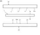
しかしながら、上記の特許文献1〜3に開示されている方法では、図22(a),(b)に示すように、マザー基板300の一方側の表面300aに、ブレイク用の分割溝301を形成し、この分割溝を起点としてマザー基板300をブレイクするように構成されており、マザー基板の片側表面にしかブレイクの起点がないため、意図したとおり、分割端面302がマザー基板300の表面300aに垂直になるようにマザー基板300を分割することは困難で、図23に模式的に示すように、分割端面302が主面に垂直にはならずに、斜めになってしまう場合がある。
However, in the methods disclosed in the
その結果、分割することにより得られる個々のセラミック基板の外観や寸法に不良が生じたり、セラミック基板が、例えば、内部電極を有する多層セラミック基板などである場合には、内部電極の露出などの致命欠陥が生じたりするという問題点がある。 As a result, when the appearance and dimensions of the individual ceramic substrates obtained by dividing are defective, or when the ceramic substrate is, for example, a multilayer ceramic substrate having internal electrodes, it is fatal such as exposure of internal electrodes. There is a problem that defects occur.
また、ブレイクの起点となる分割溝が浅いほど、斜めに割れるおそれが増え、逆に分割溝が深すぎると、取り扱いの際にセラミック基板が意図せずに割れてしまうというようなトラブルを招く場合がある。 In addition, the shallower the dividing groove that is the starting point of the break, the more likely it is to break diagonally, and conversely, if the dividing groove is too deep, the ceramic substrate may be unintentionally cracked during handling. There is.
また、近年、マザーセラミック基板状態の板状のフェライト焼結体(フェライトシート)を多数個の個片に分割したものが、電磁波の遮断・吸収を行うための電磁波遮断・吸収材や、RFIDやNFCのアンテナ装置などに用いられている。なお、このようなフェライトシートは、必要に応じてその片側ないし両側に保持シートを貼り付けて用いられることがある。保持シートは1つの個片について1つ貼り付けられる場合のほか、複数の個片について1つ貼り付けられているものも存在する。
上述の板状のフェライト焼結体(フェライトシート)を多数個の個片に分割することができるようにするために、その片面に分割溝を形成することが行われている。
Further, in recent years, a plate-like ferrite sintered body (ferrite sheet) in a state of a mother ceramic substrate is divided into a large number of pieces, and an electromagnetic wave blocking / absorbing material for blocking / absorbing electromagnetic waves, RFID, Used in NFC antenna devices. Such a ferrite sheet may be used with a holding sheet attached to one side or both sides as necessary. In addition to the case where one holding sheet is affixed for one piece, there is also a case where one holding sheet is affixed for a plurality of pieces.
In order to be able to divide the plate-like ferrite sintered body (ferrite sheet) into a large number of individual pieces, a dividing groove is formed on one surface thereof.
しかし、近年、このような用途に用いられるフェライト焼結体(フェライトシート)の薄型化(例えば200μm厚み以下)が進行しており、適正な深さの分割溝を形成することが困難になっており、分割溝が深すぎると、焼成前にフェライトシートが分割されてしまい、浅すぎると、分割溝に沿って正しくブレイクすることができず、例えば、ブレイク時に細かく割れてしまい特性が低下するというような問題点がある。 However, in recent years, thinning of ferrite sintered bodies (ferrite sheets) used for such applications (for example, 200 μm thickness or less) has progressed, and it has become difficult to form divided grooves with an appropriate depth. If the dividing groove is too deep, the ferrite sheet will be divided before firing, and if it is too shallow, it will not be able to break correctly along the dividing groove, for example, it will break finely at the time of breaking and the characteristics will be reduced There are some problems.
本発明は、上記課題を解決するものであり、分割して、個々の基板(セラミック基板)としたときの、分割端面が個々の基板の主面に垂直になるように分割することが可能で、形状精度の高いセラミック基板を得ることが可能なマザーセラミック基板、それを分割することにより得られる個々のセラミック基板、該マザーセラミック基板を用いたマザーモジュール部品、それを分割することにより得られるモジュール部品、および、マザーセラミック基板の製造方法を提供することを目的とする。 The present invention solves the above problems, and when divided into individual substrates (ceramic substrates), it is possible to divide the substrate so that the divided end faces are perpendicular to the main surfaces of the individual substrates. Mother ceramic substrate capable of obtaining ceramic substrate with high shape accuracy, individual ceramic substrate obtained by dividing it, mother module component using the mother ceramic substrate, module obtained by dividing it An object of the present invention is to provide a component and a method for manufacturing a mother ceramic substrate.
上記の課題を解決するため、本発明のマザーセラミック基板は、
所定の位置で分割して、複数個の個基板に分けることができるように構成されたマザーセラミック基板であって、
一方側主面に、分割位置を規定する分割溝が形成され、
他方側主面の、該マザーセラミック基板を厚み方向からみた場合に前記一方側主面の前記分割溝が形成された位置に対応する位置に、当該マザーセラミック基板自体を突出させた凸条が形成されていること
を特徴としている。
In order to solve the above problems, the mother ceramic substrate of the present invention is
A mother ceramic substrate configured to be divided at a predetermined position and divided into a plurality of individual substrates,
A dividing groove for defining a dividing position is formed on one side main surface,
On the other side main surface, when the mother ceramic substrate is viewed from the thickness direction , a ridge that projects the mother ceramic substrate itself is formed at a position corresponding to the position where the dividing groove is formed on the one side main surface. It is characterized by being.
また、本発明のマザーセラミック基板においては、分割後に得られる前記個基板がそれぞれ内部導体を備えた構成となるような態様で、内部導体を備えていることが好ましい。 Moreover, in the mother ceramic substrate of the present invention, it is preferable that the individual substrates obtained after the division have internal conductors in such a manner that the individual substrates each have internal conductors.
上述のように、分割後に得られる個基板がそれぞれ内部導体を備えた構成となるようにした場合、内部に回路や電極などの導体を備えたセラミック基板を効率よく製造することが可能になる。 As described above, when the individual substrates obtained after the division are each configured to include an internal conductor, it is possible to efficiently manufacture a ceramic substrate including an internal conductor such as a circuit or an electrode.
また、本発明のセラミック基板は、上記本発明のマザーセラミック基板を前記分割溝に沿って分割することにより得られる前記個基板であることを特徴としている。 The ceramic substrate of the present invention is characterized in that it is the individual substrate obtained by dividing the mother ceramic substrate of the present invention along the dividing grooves.
また、本発明のマザーモジュール部品は、上記本発明のマザーセラミック基板の、分割後に個基板となる領域のそれぞれに表面実装部品が搭載されていること
を特徴としている。
Further, the mother module component of the present invention is characterized in that a surface mount component is mounted on each of the regions of the mother ceramic substrate of the present invention that will become individual substrates after division.
また、本発明のモジュール部品は、上記本発明のマザーモジュール部品を、前記マザーセラミック基板の前記分割溝に沿って分割することにより得られるものであることを特徴としている。 The module component of the present invention is obtained by dividing the mother module component of the present invention along the dividing groove of the mother ceramic substrate.
また、本発明のマザーセラミック基板の製造方法は、
上記本発明のマザーセラミック基板を製造するための方法であって、
表面に凸条部が形成された第1の金型と、表面の前記第1の金型の前記凸条部と正対する位置に溝部が形成された第2の金型を用い、
未焼成のマザーセラミック基板の一方側主面に、前記第1の金型の前記凸条部が形成された面を当接させ、他方側主面に、前記第2の金型の前記溝部が形成された面を当接させ、前記第1の金型と前記第2の金型とによりプレス加工を行うことにより、前記未焼成のマザーセラミック基板の一方側主面に前記分割溝を形成するとともに、他方側主面の、該マザーセラミック基板を厚み方向からみた場合に前記一方側主面の前記分割溝が形成された位置に対応する位置に、当該マザーセラミック基板自体が突出した凸条を形成する工程と、
前記分割溝および前記凸条が形成された前記未焼成のマザーセラミック基板を焼成する工程と
を備えていることを特徴としている。
In addition, the method for manufacturing the mother ceramic substrate of the present invention includes:
A method for producing the mother ceramic substrate of the present invention,
Using a first mold having a ridge formed on the surface and a second mold having a groove formed at a position facing the ridge of the first mold on the surface,
The surface of the first mold on which the protrusions are formed is brought into contact with one side main surface of the unfired mother ceramic substrate, and the groove portion of the second mold is formed on the other side main surface. The divided grooves are formed in the main surface on one side of the unfired mother ceramic substrate by bringing the formed surface into contact with each other and pressing the first die and the second die. And, when the mother ceramic substrate on the other side main surface is viewed from the thickness direction, a ridge from which the mother ceramic substrate itself protrudes at a position corresponding to the position where the dividing groove is formed on the one side main surface. Forming, and
Firing the green mother ceramic substrate on which the dividing grooves and the protrusions are formed.
また、本発明の他のマザーセラミック基板の製造方法は、
上記本発明のマザーセラミック基板を製造するための方法であって、
未焼成のマザーセラミック基板の一方側主面に、凸条部が形成された金型の前記凸条部が形成された面を当接させ、他方側主面に弾性体を当接させた状態で静水圧プレスを行い、前記未焼成のマザーセラミック基板の一方側主面に前記分割溝を形成するとともに、他方側主面の、該マザーセラミック基板を厚み方向からみた場合に前記一方側主面の前記分割溝が形成された位置に対応する位置に、当該マザーセラミック基板自体が突出した凸条を形成する工程と、
前記分割溝および前記凸条が形成された前記未焼成のマザーセラミック基板を焼成する工程と
を備えていることを特徴としている。
In addition, another method for manufacturing a mother ceramic substrate of the present invention includes:
A method for producing the mother ceramic substrate of the present invention,
A state in which the surface of the mold having the ridges formed thereon is in contact with one side main surface of the unfired mother ceramic substrate, and an elastic body is in contact with the other side main surface And then forming the dividing groove on one main surface of the unfired mother ceramic substrate, and the one main surface of the other main surface when the mother ceramic substrate is viewed from the thickness direction. Forming a protrusion on which the mother ceramic substrate itself protrudes at a position corresponding to the position where the dividing groove is formed,
Firing the green mother ceramic substrate on which the dividing grooves and the protrusions are formed.
また、本発明のさらに他のマザーセラミック基板の製造方法は、
上記本発明のマザーセラミック基板を製造するための方法であって、
未焼成のマザーセラミック基板の一方側主面に、凸条部が形成された金型の前記凸条部が形成された面を当接させ、他方側主面に弾性体を介して剛体を配設した状態でプレス加工を行い、前記未焼成のマザーセラミック基板の一方側主面に前記分割溝を形成するとともに、他方側主面の、該マザーセラミック基板を厚み方向からみた場合に前記一方側主面の前記分割溝が形成された位置に対応する位置に、当該マザーセラミック基板自体が突出した凸条を形成する工程と、
前記分割溝および前記凸条が形成された前記未焼成のマザーセラミック基板を焼成する工程と
を備えていることを特徴としている。
Further, another method for producing a mother ceramic substrate of the present invention includes:
A method for producing the mother ceramic substrate of the present invention,
The surface of the mold on which the ridges are formed is brought into contact with one side main surface of the unfired mother ceramic substrate, and a rigid body is arranged on the other side main surface via an elastic body. In the installed state, the one side main surface of the unfired mother ceramic substrate is formed with the dividing grooves, and the other side main surface of the mother ceramic substrate is viewed from the thickness direction when the mother ceramic substrate is viewed from the thickness direction. Forming a ridge from which the mother ceramic substrate itself protrudes at a position corresponding to the position where the dividing groove is formed on the main surface;
Firing the green mother ceramic substrate on which the dividing grooves and the protrusions are formed.
また、本発明のさらに他のマザーセラミック基板の製造方法は、
上記本発明のマザーセラミック基板を製造するための方法であって、
未焼成のマザーセラミック基板の一方側主面に、溝部が形成された金型の前記溝部が形成された面を当接させ、プレス加工を行うことにより、前記未焼成のマザーセラミック基板の前記一方側主面に、当該マザーセラミック基板自体が突出した凸条を形成する工程と、
前記未焼成のマザーセラミック基板の他方側主面の、該マザーセラミック基板を厚み方向からみた場合に前記一方側主面の前記凸条が形成された位置に対応する位置に前記分割溝を形成するための加工を行う工程と、
前記分割溝および前記凸条が形成された前記未焼成のマザーセラミック基板を焼成する工程と
を備えていることを特徴としている。
Further, another method for producing a mother ceramic substrate of the present invention includes:
A method for producing the mother ceramic substrate of the present invention,
The one side main surface of the unfired mother ceramic substrate is brought into contact with the surface on which the groove portion is formed, and the one side of the unfired mother ceramic substrate is pressed. On the side main surface, forming a protrusion from which the mother ceramic substrate itself protrudes ;
The dividing groove is formed at a position corresponding to a position on the other side main surface of the unfired mother ceramic substrate corresponding to the position where the protrusions are formed on the one side main surface when the mother ceramic substrate is viewed from the thickness direction. A process for performing the process,
Firing the green mother ceramic substrate on which the dividing grooves and the protrusions are formed.
また、本発明のセラミック基板は、
平面形状が方形であり、一方側主面と他方側主面とを有するセラミック基板であって、
前記他方側主面の4辺のうち、少なくとも1辺は、当該セラミック基板自体が突出した凸条を有し、
前記一方側主面の4辺のうち、前記セラミック基板を厚み方向からみた場合に前記他方側主面の前記凸条が形成された位置に対応する位置の辺は、稜部が面取りされていること
を特徴としている。
In addition, the ceramic substrate of the present invention,
A ceramic substrate having a square planar shape and having one main surface and the other main surface,
Of the four sides of the other side main surface, at least one side has a ridge from which the ceramic substrate itself protrudes ,
Of the four sides of the one side main surface, when the ceramic substrate is viewed from the thickness direction, the side of the side corresponding to the position where the convex line is formed on the other side main surface is chamfered. It is characterized by this.
本発明のマザーセラミック基板は、一方側主面に分割位置を規定する分割溝が形成され、他方側主面の、マザーセラミック基板を厚み方向からみた場合に一方側主面の分割溝が形成された位置に対応する位置に、当該マザーセラミック基板自体を突出させた凸条が形成されているので、以下のような作用効果を奏する。 In the mother ceramic substrate of the present invention, a dividing groove for defining a dividing position is formed on one main surface, and a dividing groove on one main surface is formed on the other main surface when the mother ceramic substrate is viewed from the thickness direction. Since the protrusions from which the mother ceramic substrate itself protrudes are formed at positions corresponding to the above positions, the following operational effects can be obtained.
分割溝に沿って分割する際に、マザーセラミック基板の主面に対してほぼ垂直に分割することができる。
マザーセラミック基板を分割する際には、一方側主面に形成された分割溝がブレイクの起点となるようにマザーセラミック基板を湾曲させる力が加えられる。
このとき、他方側主面に形成された凸条(山部)の裾に応力を集中させることができる。その結果、マザーセラミック基板を分割する際に、一方側主面の分割溝から進展するクラックが、他方側主面の対向位置にある凸条(山部)の裾に導かれる。
そして、凸条の幅は、マザーセラミック基板の厚みに比べて小さいので、図5(a)に示すように、クラックCが伸びることにより分割されたマザーセラミック基板1の分割端面(分割後のセラミック基板の端面でもある)31aは、マザーセラミック基板の主面に対してほぼ垂直になる。
When dividing along the dividing groove, it can be divided substantially perpendicular to the main surface of the mother ceramic substrate.
When the mother ceramic substrate is divided, a force is applied to curve the mother ceramic substrate so that the dividing groove formed on the one side main surface becomes the starting point of the break.
At this time, stress can be concentrated on the bottom of the ridge (mountain) formed on the other main surface. As a result, when the mother ceramic substrate is divided, cracks that develop from the dividing grooves on the one side main surface are guided to the skirts of the ridges (mountains) at the opposing positions on the other side main surface.
And since the width | variety of a protruding item | line is small compared with the thickness of a mother ceramic substrate, as shown to Fig.5 (a), as shown in Fig.5 (a), the division | segmentation end surface (ceramic after division | segmentation) of the mother
なお、本発明のマザーセラミック基板においては、一方側主面に分割溝を形成し、他方側主面に凸条を設けているので、分割溝の深さと、凸条の高さが数μm程度であっても(すなわち、分割溝の深さに依存することなく)、確実にマザーセラミック基板の主面に対してほぼ垂直に分割(破断)することができる。 In the mother ceramic substrate of the present invention, the dividing grooves are formed on the one side main surface and the ridges are provided on the other side main surface. Therefore, the depth of the dividing grooves and the height of the ridges are about several μm. Even in this case (that is, without depending on the depth of the dividing groove), it can be surely divided (broken) substantially perpendicular to the main surface of the mother ceramic substrate.
また、分割溝を浅くすることができるため、焼成前の取り扱いの際に、マザーセラミック基板が意図せずに分割されてしまうことを防止することができる。 Moreover, since the dividing groove can be made shallow, it is possible to prevent the mother ceramic substrate from being unintentionally divided during handling before firing.
また、マザーセラミック基板が、例えば、電磁波の遮断・吸収を行うための電磁波遮断・吸収材や、RFIDやNFCのアンテナ装置に用いられるフェライトシートとしてのセラミック基板(フェライト個基板)に用いられるものである場合にも、分割端面が垂直になるため、分割後集合状態でハンドリングする際などにフェライト個基板の端面どうしがこすれて、フェライト粉末が発生する(粉落する)ことによる粉塵の発生を招くことがない。
また、例えば、凸条が形成された他方側主面を保持フィルム(粘着テープ)に貼り付けて用いる場合、凸条がアンカーとして保持フィルムに食い込むことから、分割されたフェライト個基板が、保持フィルムの屈曲時に脱落することを抑制して、信頼性を向上させることができる。
The mother ceramic substrate is used for, for example, an electromagnetic wave blocking / absorbing material for blocking / absorbing electromagnetic waves, or a ceramic substrate (ferrite individual substrate) as a ferrite sheet used in an RFID or NFC antenna device. Even in some cases, the split end faces are vertical, so when handling in the assembled state after splitting, the end faces of the ferrite substrate are rubbed and lead to generation of dust due to the generation of ferrite powder (dusting). There is nothing.
In addition, for example, when the other main surface on which the ridges are formed is attached to a holding film (adhesive tape), the ridges bite into the holding film as anchors. It is possible to improve the reliability by suppressing falling off during bending.
また、本発明のセラミック基板は、上記本発明のマザーセラミック基板を分割溝に沿って分割することにより得られる個基板(セラミック基板)であり、分割端面がマザーセラミック基板の主面(=個々のセラミック基板の主面)に垂直で、形状精度が高く、種々の用途に広く用いることができる。 Further, the ceramic substrate of the present invention is an individual substrate (ceramic substrate) obtained by dividing the mother ceramic substrate of the present invention along the dividing groove, and the divided end surface is the main surface (= individual surface) of the mother ceramic substrate. It is perpendicular to the main surface of the ceramic substrate), has high shape accuracy, and can be widely used in various applications.
また、本発明のマザーモジュール部品は、上記本発明のマザーセラミック基板の、分割後に個基板となる領域のそれぞれに表面実装部品が搭載されているため、分割溝に沿って分割するだけで、容易かつ確実に、信頼性の高いモジュール部品を得ることができる。 In addition, since the mother module component of the present invention has surface-mounted components mounted on each of the regions of the mother ceramic substrate of the present invention that become individual substrates after the division, it is easy to divide along the dividing groove. And reliable module parts can be obtained reliably.
また、本発明のマザーセラミック基板の製造方法は、表面に凸条部が形成された第1の金型と、表面の第1の金型の凸条部と正対する位置に溝部が形成された第2の金型を用い、未焼成のマザーセラミック基板の一方側主面に、第1の金型の凸条部が形成された面を当接させ、他方側主面に、第2の金型の溝部が形成された面を当接させ、第1の金型と第2の金型とによりプレス加工を行うようにしているので、一方側主面に分割溝が形成され、他方側主面の、上記分割溝が形成された位置に対応する位置に、当該マザーセラミック基板自体を突出させた凸条が形成された未焼成のマザーセラミック基板を確実に作製することができる。
そして、この未焼成のマザーセラミック基板を焼成することにより、焼結済みで、一方側主面に分割溝を備え、他方側主面に凸条を備えたマザーセラミック基板を効率よく、しかも確実に製造することができる。
Further, in the method for manufacturing a mother ceramic substrate according to the present invention, the groove is formed at a position where the first mold having the protrusions formed on the surface and the protrusions of the first mold on the surface are opposed to each other. Using the second mold, the surface on which the protruding portion of the first mold is formed is brought into contact with one side main surface of the unfired mother ceramic substrate, and the second mold is formed on the other side main surface. Since the surface where the groove portion of the mold is formed is brought into contact and pressing is performed by the first mold and the second mold, a split groove is formed on one side main surface, and the other side main surface is formed. An unfired mother ceramic substrate can be reliably produced in which protrusions that project the mother ceramic substrate itself are formed at positions on the surface corresponding to the positions where the dividing grooves are formed.
And by firing this unfired mother ceramic substrate, it is sintered, and the mother ceramic substrate having a split groove on one side main surface and a ridge on the other side main surface is efficiently and reliably obtained. Can be manufactured.
また、本発明の他のマザーセラミック基板の製造方法のように、未焼成のマザーセラミック基板の一方側主面に金型の凸条部が形成された面を当接させ、他方側主面に弾性体を当接させた状態で静水圧プレスを行うようにした場合にも、一方側主面に分割溝が形成され、他方側主面の、上記分割溝が形成された位置に対応する位置に、当該マザーセラミック基板自体を突出させた凸条が形成された未焼成のマザーセラミック基板を確実に作製することが可能になり、これを焼成することにより、焼結済みで、一方側主面に分割溝を備え、他方側主面に凸条を備えたマザーセラミック基板を効率よく、しかも確実に製造することができる。
なお、他方側主面の、上記分割溝が形成された位置に対応する位置に凸条が形成されるのは、金型の凸条部からマザーセラミック基板に加わる圧力により、一方側主面には分割溝が形成されるとともに、他方側主面にまでその力が伝わり、凸条部が形成されることによる。
In addition, as in the other method of manufacturing a mother ceramic substrate of the present invention, the surface on which the convex portion of the mold is formed is brought into contact with one side main surface of the unfired mother ceramic substrate, and the other side main surface is contacted. Even when the hydrostatic pressing is performed in a state where the elastic body is in contact, a position corresponding to the position where the dividing groove is formed on the one side main surface and the dividing groove is formed on the other side main surface. In addition, it is possible to reliably produce an unfired mother ceramic substrate on which protrusions projecting from the mother ceramic substrate itself are formed. A mother ceramic substrate having a dividing groove on the other side and a protrusion on the other main surface can be produced efficiently and reliably.
The ridges are formed on the other side main surface at positions corresponding to the positions where the dividing grooves are formed on the one side main surface by the pressure applied to the mother ceramic substrate from the ridges of the mold. This is because the split groove is formed, the force is transmitted to the other main surface, and the ridge is formed.
また、本発明のさらに他のマザーセラミック基板の製造方法のように、未焼成のマザーセラミック基板の一方側主面に、凸条部が形成された金型の凸条部が形成された面を当接させ、他方側主面に弾性体を介して剛体を配設した状態でプレス加工を行うようにした場合にも、一方側主面に分割溝が形成され、他方側主面の、上記分割溝が形成された位置に対応する位置に、当該マザーセラミック基板自体を突出させた凸条が形成された未焼成のマザーセラミック基板を確実に作製することが可能になり、これを焼成することにより、焼結済みで、一方側主面に分割溝を備え、他方側主面に凸条を備えたマザーセラミック基板を効率よく、しかも確実に製造することができる。 Further, as in still another method of manufacturing a mother ceramic substrate according to the present invention, a surface on which a convex strip portion of a mold in which a convex strip portion is formed is formed on one side main surface of an unfired mother ceramic substrate. Even when pressing is performed in a state where a rigid body is disposed on the other side main surface via an elastic body, a split groove is formed on the one side main surface, and the other side main surface is It becomes possible to reliably produce an unfired mother ceramic substrate in which protrusions that project the mother ceramic substrate itself are formed at positions corresponding to the positions where the division grooves are formed, and firing this Thus, it is possible to efficiently and surely manufacture a mother ceramic substrate that has been sintered and has a dividing groove on one side main surface and a protrusion on the other side main surface.
また、本発明のさらに他のマザーセラミック基板の製造方法のように、未焼成のマザーセラミック基板の一方側主面に、溝部が形成された金型の溝部が形成された面を当接させてプレス加工を行い、マザーセラミック基板の一方側主面に凸条を形成した後、他方側主面に分割溝を形成するための加工(溝形成加工)(例えば、切削加工など)を行うようにした場合にも、一方側主面に分割溝が形成され、他方側主面の、上記分割溝が形成された位置に対応する位置に、当該マザーセラミック基板自体を突出させた凸条が形成された未焼成のマザーセラミック基板を確実に作製することが可能になり、これを焼成することにより、焼結済みで、一方側主面に分割溝を備え、他方側主面に凸条を備えたマザーセラミック基板を効率よく、しかも確実に製造することができる。 Further, as in still another method of manufacturing a mother ceramic substrate according to the present invention, the surface of the mold on which the groove is formed is brought into contact with the main surface on one side of the unfired mother ceramic substrate. After pressing and forming a ridge on one main surface of the mother ceramic substrate, processing (groove forming processing) (for example, cutting processing) for forming split grooves on the other main surface is performed. In this case, a dividing groove is formed on the one side main surface, and a protrusion that projects the mother ceramic substrate itself is formed on the other side main surface at a position corresponding to the position where the dividing groove is formed. It was possible to reliably produce an unfired mother ceramic substrate, and by firing this, it was sintered and provided with a dividing groove on one side main surface and provided with a ridge on the other side main surface. Efficient and reliable mother ceramic substrate It can be produced in.
なお、本発明において、分割溝や凸条はV字形状(逆V字形状)であることが好ましいが、U字形条(逆U字形状)などの他の形状であってもよい。 In the present invention, the dividing grooves and the ridges are preferably V-shaped (inverted V-shaped), but may be other shapes such as U-shaped (inverted U-shaped).
以下に本発明の実施形態を示して、本発明の特徴とするところをさらに詳しく説明する。 Embodiments of the present invention will be described below to describe the features of the present invention in more detail.
[実施形態1]
この実施形態1では、セラミック材料として、磁性体セラミックを用いたセラミック基板(フェライト基板)の製造方法について説明する。
[Embodiment 1]
In the first embodiment, a method for manufacturing a ceramic substrate (ferrite substrate) using a magnetic ceramic as a ceramic material will be described.
(1)まず、磁性体セラミック粉末(この実施形態1ではフェライト粉末)とバインダー樹脂と有機溶剤とを混合して、溶解、分散させた後、脱泡することにより、セラミック原料スラリーを作製した。 (1) First, a ceramic raw material slurry was prepared by mixing, dissolving and dispersing a magnetic ceramic powder (ferrite powder in this embodiment 1), a binder resin, and an organic solvent, followed by defoaming.
それから、このセラミック原料スラリーを、ドクターブレード法などの公知の方法により、シート状に成形し、乾燥することにより、厚さ200μmのマザーセラミックグリーンシートを作製した。
なお、マザーセラミックグリーンシートは、複数枚のセラミックグリーンシートが積層された積層体であってもよい。
Then, this ceramic raw material slurry was formed into a sheet shape by a known method such as a doctor blade method and dried to prepare a mother ceramic green sheet having a thickness of 200 μm.
The mother ceramic green sheet may be a laminate in which a plurality of ceramic green sheets are laminated.
それから、得られたマザーセラミックグリーンシートを所定の大きさにカットすることにより、本発明における未焼成のマザーセラミック基板である、カット済みのマザーセラミックグリーンシートを得た。 Then, the obtained mother ceramic green sheet was cut into a predetermined size to obtain a cut mother ceramic green sheet which is an unfired mother ceramic substrate in the present invention.
(2)次に、図1に示すように、所定の大きさにカットされたマザーセラミックグリーンシート(未焼成のマザーセラミック基板)1を、表面10aに凸条部11が形成された第1の金型10と、表面20aに溝部21が形成された第2の金型20の間に位置させ、図2に示すように、第1の金型10および第2の金型20によりプレスした。これにより、一方側主面2aに分割溝3が形成され、他方側主面2bに凸条4が形成されたプレス後のマザーセラミック基板1(1A)(図3)を得た。
(2) Next, as shown in FIG. 1, a mother ceramic green sheet (unfired mother ceramic substrate) 1 cut to a predetermined size is formed on the
なお、この実施形態では、第1の金型10として、図4Aに示すように、表面10aに、高さが約5μmで、幅が約20μmの山形の凸条部11が、格子状に形成された構造のものを用いた。
In this embodiment, as shown in FIG. 4A, the
また、第2の金型20として、図4Bに示すように、表面20aに、深さが約5μmで、幅が約20μmのV字状の溝部21が、格子状に形成された構造のものを用いた。
As shown in FIG. 4B, the
第1の金型10と第2の金型20を用いてプレスを行うにあたっては、マザーセラミック基板1を厚み方向からみた場合に、第1の金型10の表面10aに形成された凸条部11が形成された位置に対応する位置に、第2の金型20の表面20aに形成されたV字状の溝部21が位置するように、第1の金型10と第2の金型20の位置関係を調節してプレスを行った(図2参照)。
When pressing using the
(3)それから、プレス後のマザーセラミック基板1(1A)を、950℃で焼成することで、焼結済みのマザーセラミック基板(フェライト焼結基板)1(1B)を得た。 (3) Then, the mother ceramic substrate 1 (1A) after pressing was fired at 950 ° C. to obtain a sintered mother ceramic substrate (ferrite sintered substrate) 1 (1B).
(4)次に、焼結済みのマザーセラミック基板1(1B)を、例えば、ローラーブレイクなどの方法で分割処理を施し、分割溝3に沿って分割した。このとき、図5(a)に示すように、一方側主面2aの分割溝3において発生したクラックCは、他方側主面2bの凸条4の裾に向かって伸びる。
(4) Next, the mother ceramic substrate 1 (1B) that had been sintered was subjected to a dividing process by a method such as roller break, and divided along the dividing
そして、凸条4の幅は、マザーセラミック基板1(1B)の厚みに比べて小さいので、クラックCが伸びることにより分割された後に得られるセラミック基板31の分割端面31aは、セラミック基板31の主面(=マザーセラミックグリーンシートの一方側主面2a,他方側主面2b)に対してほぼ垂直になる。
Since the width of the
その結果、マザーセラミック基板1(1B)を分割溝3に沿って分割することにより、分割端面31aがセラミック基板31の主面(=マザーセラミックグリーンシートの一方側主面2a,他方側主面2b)に対してほぼ垂直なセラミック基板31が得られる(図5(b)参照)。
As a result, by dividing the mother ceramic substrate 1 (1B) along the dividing
このとき、図5(b)に示すセラミック基板31は、一方側主面(上面)の左右の稜部が、上述の分割溝3a(図5(a))が最深部で分割されることにより形成される面取りされた形状となり、また、他方側主面(下面)の一方側の端部(図5(b)では左側の端部)には、上述の凸条4が存在している。なお、一方側の端部(図5(b)では左側の端部)にのみ、上述の凸条4が存在するのは、上述のように、一方側主面2aの分割溝3において発生したクラックCが、他方側主面2bの凸条4の裾に向かって伸びることによるものである。
ただし、凸条4が、主要部と残りの一部とに分割されるような態様で上記クラックCが伸びた場合には、他方側主面(下面)の一方側の端部と他方側の端部のそれぞれに、分割された上記凸条4の一部が存在することもある。
At this time, in the
However, when the crack C extends in such a manner that the
なお、本発明のマザーセラミック基板1(1B)においては、一方側主面2aに分割溝3を形成し、他方側主面2bに凸条4を設けているので、分割溝3の深さと、凸条4の高さが数μm程度であっても、確実にマザーセラミック基板1(1B)の主面(一方側主面2a、他方側主面2b)に対してほぼ垂直に分割(破断)することができる。
In the mother ceramic substrate 1 (1B) of the present invention, the dividing
このように、マザーセラミック基板1(1B)を分割することにより得られるセラミック基板31は、分割端面31aが個々のセラミック基板31の主面に垂直で、形状精度が高く、種々の用途に広く用いることができるものである。
Thus, the
また、図6(a)に示すように、焼結済みのマザーセラミック基板1(1B)の凸条4が形成された面である他方側主面2bに、例えば、保持フィルムとして機能する粘着テープ5を貼り付けた状態で、例えば、ローラーブレイクなどの方法で分割処理を施し、分割溝3に沿って分割し(図6(b))、その後粘着テープ5を剥がすことにより、分割端面31aが主面に垂直なセラミック基板31を得るようにすることもできる。このようなセラミック基板31のそれぞれ(個基板)は、RFIDやNFCのアンテナ装置用の磁性体セラミック基板として好適に用いることができる。
なお、保持フィルムとして機能する粘着テープ5を剥がさずに貼り付けたまま用いることも可能である。その場合、複数個が集合状態で保持フィルム5上に保持され、全体として柔軟性を備えたフェライトシートとして使用することが可能なセラミック基板31を得ることができる。このようなフェライトシートとしてのセラミック基板31は電磁波の遮断・吸収を行うための電磁波遮断・吸収材として好適に用いることができる。
上記のいずれの場合においても、複数個が集合状態で保持フィルム5上に保持された集合体としてのセラミック基板31は、例えば集合状態でハンドリングする際に図6(c)に示すように、意図的にまたは意図せず全体を湾曲したり、球面状に変形したりすることが考えられる。その場合にも、保持フィルム5の屈曲時に個々のセラミック基板(フェライト基板)31の端面(分割端面)どうしがこすれて、フェライト粉末が発生する(粉落する)ことによる粉塵の発生を招くことがない。これにより、電磁波遮断・吸収材や、RFIDやNFCのアンテナ装置などに好適に用いることができる。
Moreover, as shown to Fig.6 (a), the adhesive tape which functions as a holding film, for example on the other side
In addition, it is also possible to use the
In any of the above cases, the
[実施形態2]
この実施形態2では、セラミック材料として、低温焼結セラミックを用いたセラミック基板(多層セラミック基板)の製造方法について説明する。
[Embodiment 2]
In the second embodiment, a method for manufacturing a ceramic substrate (multilayer ceramic substrate) using a low-temperature sintered ceramic as a ceramic material will be described.
(1)まず、ガラスセラミック粉末(低温焼結セラミック粉末)とバインダー樹脂と有機溶剤とを混合して、溶解、分散させた後、脱泡することにより、セラミック原料スラリーを作製した。 (1) First, glass ceramic powder (low-temperature sintered ceramic powder), a binder resin, and an organic solvent were mixed, dissolved and dispersed, and then defoamed to prepare a ceramic raw material slurry.
それから、このセラミック原料スラリーを、ドクターブレード法などの公知の方法により、シート状に成形し、乾燥することにより、厚さ50μmのマザーセラミックグリーンシートを複数枚作製した。 Then, the ceramic raw material slurry was formed into a sheet by a known method such as a doctor blade method and dried to produce a plurality of mother ceramic green sheets having a thickness of 50 μm.
次に、このセラミック原料スラリーを、ドクターブレード法などの公知の方法により、シート状に成形し、乾燥することにより、厚さ50μmの単一マザーセラミックグリーンシートを複数枚作製した。 Next, the ceramic raw material slurry was formed into a sheet shape by a known method such as a doctor blade method and dried to prepare a plurality of single mother ceramic green sheets having a thickness of 50 μm.
それから、得られたマザーセラミックグリーンシートを所定の大きさにカットし、それぞれに内部電極形成用の導電性ペースト(Agペースト)をスクリーン印刷して、内部電極パターンを形成した。なお、必要に応じてマザーセラミックグリーンシートに貫通孔を形成し、導電性ペーストを充填することによりビア導体(内部電極の1種)を備えたマザーセラミックグリーンシートとすることも可能である。 Then, the obtained mother ceramic green sheet was cut into a predetermined size, and an internal electrode forming conductive paste (Ag paste) was screen printed on each to form an internal electrode pattern. Note that a mother ceramic green sheet provided with via conductors (one type of internal electrodes) can be formed by forming through holes in the mother ceramic green sheet as required and filling with a conductive paste.
続いて、この内部電極パターンを備えたマザーセラミックグリーンシートを所定の順序で積層することにより、図7に示すように、内部電極6を備えた未焼成のマザーセラミック基板(マザーセラミックグリーンシートの積層体)1を得た。 Subsequently, the mother ceramic green sheets provided with the internal electrode patterns are laminated in a predetermined order, whereby a non-fired mother ceramic substrate provided with the internal electrodes 6 (lamination of the mother ceramic green sheets) as shown in FIG. Body) 1 was obtained.
(2)それから、このマザーセラミック基板1を、上記実施形態1の場合と同じ金型を用い、同じ方法でプレスして、図8に示すように、一方側主面2aに分割溝3が形成され、他方側主面2bに凸条4が形成されたプレス後のマザーセラミック基板1(1A)を得た。図8はプレス後に、第1の金型10と第2の金型20を、マザーセラミック基板1(1A)から分離した状態を示している。
(2) Then, the mother
(3)それから、プレス後のマザーセラミック基板1(1A)を、900℃で焼成することにより、焼結済みのマザーセラミック基板1(1B)を得た。 (3) Then, the mother ceramic substrate 1 (1A) after pressing was fired at 900 ° C. to obtain a sintered mother ceramic substrate 1 (1B).
(4)次に、焼結済みのマザーセラミック基板1(1B)を、例えば、ローラーブレイクなどの方法で分割処理を施し、分割溝3に沿って分割することにより、図9に示すような、個々のセラミック基板(多層セラミック基板)31を得た。
なお、上述のマザーセラミック基板1(1B)を分割することにより得られるセラミック基板(多層セラミック基板)31は、図9に示すように、分割端面(セラミック基板31の端面)31aが個々のセラミック基板31の主面に垂直で、形状精度が高く、種々の用途に広く用いることができるものである。
(4) Next, by dividing the sintered mother ceramic substrate 1 (1B) by a method such as roller break and dividing along the dividing
In addition, as shown in FIG. 9, the ceramic substrate (multilayer ceramic substrate) 31 obtained by dividing the mother ceramic substrate 1 (1B) described above has divided end surfaces (end surfaces of the ceramic substrate 31) 31a as individual ceramic substrates. It is perpendicular to the
[実施形態3]
この実施形態3では、図10に示すように、表面導体、内部導体、ビア導体などを備えたセラミック基板(多層セラミック基板)1に表面実装部品151を搭載してなるモジュール部品150の製造方法について説明する。
[Embodiment 3]
In the third embodiment, as shown in FIG. 10, a method of manufacturing a
(1)まず、上記実施形態2の場合と同様の方法でセラミックグリーンシート(低温焼結セラミックグリーンシート)1を作製し、得られたセラミックグリーンシート1に、例えば、表面導体や内部導体となる導体パターンの形成、ビアホールの形成および該ビアホールへのビア導体となる導体材料の充填などを行って、図11に示すように、必要な導体パターン140を備えたパターン形成シート101aを作製する。
(1) First, a ceramic green sheet (low-temperature sintered ceramic green sheet) 1 is prepared by the same method as in the second embodiment, and the obtained ceramic
(2)それから、導体パターン140を備えたパターン形成シート101aを所定の順序で積層し(図12)、得られた積層体を袋に入れて、脱気した後、密閉し、所定の温度に加熱した後、静水圧プレスを行うことにより、図13に示すように、各パターン形成シート101aが圧着された積層体(未焼成のマザーセラミック基板)1を得た。
(2) Then, the
(3)それから、図14に示すように、未焼成のマザーセラミック基板1を、上記実施形態1および2の場合と同じ金型を用い、同じ方法でプレスして、一方側主面2aに分割溝3が形成され、他方側主面2bに凸条4が形成されたプレス後のマザーセラミック基板1(1A)を得た。
(3) Then, as shown in FIG. 14, the unfired mother
(4)次に、プレス後のマザーセラミック基板1(1A)を、900℃で焼成することで、焼結済みのマザーセラミック基板1(1B)を得た。 (4) Next, the mother ceramic substrate 1 (1A) after pressing was fired at 900 ° C. to obtain a sintered mother ceramic substrate 1 (1B).
(5)それから、焼結済みのマザーセラミック基板1(1B)(図15)の、焼成後に個々のセラミック基板31となる各領域上に、各表面実装部品151を搭載した。
なお、表面実装部品151として、例えば、ICチップ、積層セラミックコンデンサ、チップインダクタ、チップ抵抗などが搭載される。
(5) Then, each surface-mounted
As the
(6)そして、各セラミック基板上に表面実装部品151が搭載されたマザーセラミック基板1(1B)を、分割溝3に沿って分割した(図16)。これにより、分割端面31aがその主面に垂直な、寸法精度、形状精度の高い、各セラミック基板(多層セラミック基板)31上に表面実装部品151が搭載された個々のモジュール部品150が得られる。
(6) Then, the mother ceramic substrate 1 (1B) on which the
なお、図16に示すセラミック基板(多層セラミック基板)31の場合も、一方側主面(上面)の左右の稜部が、上述の分割溝3a(図5(a)参照)が最深部で分割されることにより形成される面取りされた形状となり(図5(b)参照)、また、他方側主面(下面)の一方側の端部(図5(b)では左側の端部)には、上述の凸条4が存在しているが、図16では、稜部の面取りされた形状や他方側主面(下面)の凸条の図示は省略している。
In the case of the ceramic substrate (multilayer ceramic substrate) 31 shown in FIG. 16 as well, the left and right ridges on one main surface (upper surface) are divided at the deepest portion of the above-described dividing groove 3a (see FIG. 5A). As a result, a chamfered shape is formed (see FIG. 5 (b)), and one end of the other main surface (lower surface) (the left end in FIG. 5 (b)) Although the above-mentioned
また、上記実施形態3では多層セラミック基板上に表面実装型電子部品が搭載されたモジュール部品を例にとって説明したが、本発明は、単層のセラミック基板上に表面実装型電子部品が搭載されたモジュール部品を製造する場合にも適用することが可能である。 In the third embodiment, the module component in which the surface mount type electronic component is mounted on the multilayer ceramic substrate has been described as an example. However, in the present invention, the surface mount type electronic component is mounted on the single layer ceramic substrate. The present invention can also be applied when manufacturing module parts.
この実施形態3の方法によれば、寸法精度、形状精度の高いセラミック基板上に表面実装部品が搭載されたモジュール部品を効率よく製造することができる。 According to the method of the third embodiment, it is possible to efficiently manufacture a module component in which a surface mount component is mounted on a ceramic substrate having high dimensional accuracy and shape accuracy.
[実施形態4]
上記の実施形態1,2,3においては、凸条部が形成された第1の金型と、溝部が形成された第2の金型を用いて、マザーセラミック基板の一方側主面に分割溝を、他方側主面に凸条を形成するようにしているが、以下に説明する方法によっても、マザーセラミック基板の一方側主面に分割溝を、他方側主面に凸条を形成することが可能である。
[Embodiment 4]
In the first, second, and third embodiments described above, the first mold in which the ridges are formed and the second mold in which the grooves are formed are used to divide the main surface on one side of the mother ceramic substrate. Grooves are formed on the main surface of the other side, but also by the method described below, split grooves are formed on the main surface of one side of the mother ceramic substrate, and protrusions are formed on the main surface of the other side. It is possible.
(1)溝および凸条を形成するための他の第1の方法
図17に模式的に示すように、未焼成のマザーセラミック基板1の一方側主面2aに、凸条部51が形成された金型50の、該凸条部51が形成された面を当接させ、他方側主面2bに静水圧プレス用弾性体52を当接させた状態で全体を袋状部材53に収容し、水中にて加圧する静水圧プレスを行う。これにより、凸条部51によるプレス圧力により、未焼成のマザーセラミック基板1の一方側主面2aの凸条部51に対応する位置に分割溝3が形成されるとともに、未焼成のマザーセラミック基板1の他方側主面2bに凸条4が形成される。
なお、袋状部材53に静水圧プレス用弾性体52の機能を兼ねさせて、静水圧プレス用弾性体52を使用せずに静水圧プレスを行うことも可能であり、静水圧プレスの具体的な方法に特に制約はない。
(1) Another first method for forming grooves and ridges As shown schematically in FIG. 17, the
It is also possible to cause the bag-
この方法の場合にも、未焼成のマザーセラミック基板1の一方側主面2aに、分割位置を規定する分割溝3を形成するとともに、他方側主面2bの、未焼成のマザーセラミック基板1を厚み方向からみた場合に一方側主面2aの分割溝3が形成された位置に対応する位置に凸条4を備えたマザーセラミック基板1を形成することができる。
Also in this method, the dividing
(2)溝および凸条を形成するための他の第2の方法
図18に模式的に示すように、未焼成のマザーセラミック基板1の一方側主面2aに、凸条部51が形成された金型50の、該凸条部51が形成された面を当接させ、他方側主面2bに弾性体62を介して剛体63を配設した状態でプレス加工を行う。
(2) Another Second Method for Forming Grooves and Convex Lines As schematically shown in FIG. 18, a
この方法の場合にも、未焼成のマザーセラミック基板1の一方側主面2aに、分割位置を規定する分割溝3を形成するとともに、他方側主面2bの、未焼成のマザーセラミック基板1を厚み方向からみた場合に一方側主面2aの分割溝3が形成された位置に対応する位置に凸条4を備えたマザーセラミック基板1を形成することができる。
Also in this method, the dividing
(3)溝および凸条を形成するための他の第3の方法
図19に示すように、平坦な剛体体63上に載置した未焼成のマザーセラミック基板1の他方側主面2bに、溝部61が形成された金型60の、該溝部61が形成された面を当接させ、プレス加工を行うことにより、図20に示すように、未焼成のマザーセラミック基板1の他方側主面2bに、凸条4を形成する。
(3) Another third method for forming grooves and ridges As shown in FIG. 19, on the other
それから、図21に示すように、未焼成のマザーセラミック基板1の一方側主面2aに溝形成加工を行って、未焼成のマザーセラミック基板1の一方側主面2aの、未焼成のマザーセラミック基板1を厚み方向からみた場合に他方側主面2bの凸条4が形成された位置に対応する位置に分割溝3を形成する。
溝形成加工には、切削加工、レーザー加工などの方法を適用することが可能である。
Then, as shown in FIG. 21, a groove forming process is performed on the one-side
A method such as cutting or laser processing can be applied to the groove forming process.
この方法の場合にも、未焼成のマザーセラミック基板1の一方側主面2aに、分割位置を規定する分割溝3を形成するとともに、他方側主面2bの、未焼成のマザーセラミック基板1を厚み方向からみた場合に一方側主面2aの分割溝3が形成された位置に対応する位置に凸条4を備えたマザーセラミック基板1を形成することができる。
Also in this method, the dividing
また、上記実施形態では、分割溝および凸条がV字形状(逆V字形状)である場合を例にとって説明したが、分割溝および凸条は、U字形条(逆U字形状)などの他の形状とすることも可能である。 Moreover, although the said embodiment demonstrated as an example the case where a division | segmentation groove | channel and a protruding item | line are V-shaped (inverted V-shaped), a division | segmentation groove | channel and a protruding item | line are U-shaped (reverse U-shaped) etc. Other shapes are possible.
なお、本発明は、上記実施形態に限定されるものではなく、製造するセラミック基板の寸法や形状、製造工程で未焼成マザーセラミック基板に溝および凸条を形成する方法やそれに用いる装置の種類、焼結済みのマザーセラミック基板をブレイクする方法などに関し、発明の範囲内において、種々の応用、変形を加えることが可能である。 The present invention is not limited to the above embodiment, but the size and shape of the ceramic substrate to be manufactured, the method of forming grooves and ridges on the unfired mother ceramic substrate in the manufacturing process, and the type of apparatus used therefor, With respect to a method for breaking a sintered mother ceramic substrate, various applications and modifications can be made within the scope of the invention.
1 マザーセラミック基板
1(1A) 分割溝と凸条を備えたマザーセラミック基板
1(1B) 焼結済みのマザーセラミック基板
2a マザーセラミック基板の一方側主面
2b 他方側主面
3 分割溝
4 凸条
5 粘着テープ(保持フィルム)
6 内部電極
10 第1の金型
10a 第1の金型の表面
11 凸条部
20 第2の金型
20a 第2の金型の表面
21 溝部
31 セラミック基板
31a 分割端面(セラミック基板の端面)
50 金型
51 凸条部
52 静水圧プレス用弾性体
53 袋状部材
60 金型
61 溝部
62 弾性体
63 剛体
101a パターン形成シート
140 導体パターン
150 モジュール部品
151 表面実装部品
C クラック
DESCRIPTION OF
6
DESCRIPTION OF
Claims (10)
一方側主面に、分割位置を規定する分割溝が形成され、
他方側主面の、該マザーセラミック基板を厚み方向からみた場合に前記一方側主面の前記分割溝が形成された位置に対応する位置に、当該マザーセラミック基板自体を突出させた凸条が形成されていること
を特徴とするマザーセラミック基板。 A mother ceramic substrate configured to be divided at a predetermined position and divided into a plurality of individual substrates,
A dividing groove for defining a dividing position is formed on one side main surface,
On the other side main surface, when the mother ceramic substrate is viewed from the thickness direction , a ridge that projects the mother ceramic substrate itself is formed at a position corresponding to the position where the dividing groove is formed on the one side main surface. A mother ceramic substrate characterized by being made.
を特徴とするマザーモジュール部品。 A mother module component, wherein a surface mount component is mounted on each of the regions of the mother ceramic substrate according to claim 1 that become individual substrates after division.
表面に凸条部が形成された第1の金型と、表面の前記第1の金型の前記凸条部と正対する位置に溝部が形成された第2の金型を用い、
未焼成のマザーセラミック基板の一方側主面に、前記第1の金型の前記凸条部が形成された面を当接させ、他方側主面に、前記第2の金型の前記溝部が形成された面を当接させ、前記第1の金型と前記第2の金型とによりプレス加工を行うことにより、前記未焼成のマザーセラミック基板の一方側主面に前記分割溝を形成するとともに、他方側主面の、該マザーセラミック基板を厚み方向からみた場合に前記一方側主面の前記分割溝が形成された位置に対応する位置に、当該マザーセラミック基板自体が突出した凸条を形成する工程と、
前記分割溝および前記凸条が形成された前記未焼成のマザーセラミック基板を焼成する工程と
を備えていることを特徴とするマザーセラミック基板の製造方法。 A method for producing a mother ceramic substrate according to claim 1 or 2, comprising:
Using a first mold having a ridge formed on the surface and a second mold having a groove formed at a position facing the ridge of the first mold on the surface,
The surface of the first mold on which the protrusions are formed is brought into contact with one side main surface of the unfired mother ceramic substrate, and the groove portion of the second mold is formed on the other side main surface. The divided grooves are formed in the main surface on one side of the unfired mother ceramic substrate by bringing the formed surface into contact with each other and pressing the first die and the second die. And, when the mother ceramic substrate on the other side main surface is viewed from the thickness direction, a ridge from which the mother ceramic substrate itself protrudes at a position corresponding to the position where the dividing groove is formed on the one side main surface. Forming, and
Firing the unfired mother ceramic substrate on which the dividing grooves and the ridges are formed. A method for manufacturing a mother ceramic substrate, comprising:
未焼成のマザーセラミック基板の一方側主面に、凸条部が形成された金型の前記凸条部が形成された面を当接させ、他方側主面に弾性体を当接させた状態で静水圧プレスを行い、前記未焼成のマザーセラミック基板の一方側主面に前記分割溝を形成するとともに、他方側主面の、該マザーセラミック基板を厚み方向からみた場合に前記一方側主面の前記分割溝が形成された位置に対応する位置に、当該マザーセラミック基板自体が突出した凸条を形成する工程と、
前記分割溝および前記凸条が形成された前記未焼成のマザーセラミック基板を焼成する工程と
を備えていることを特徴とするマザーセラミック基板の製造方法。 A method for producing a mother ceramic substrate according to claim 1 or 2, comprising:
A state in which the surface of the mold having the ridges formed thereon is in contact with one side main surface of the unfired mother ceramic substrate, and an elastic body is in contact with the other side main surface And then forming the dividing groove on one main surface of the unfired mother ceramic substrate, and the one main surface of the other main surface when the mother ceramic substrate is viewed from the thickness direction. Forming a protrusion on which the mother ceramic substrate itself protrudes at a position corresponding to the position where the dividing groove is formed,
Firing the unfired mother ceramic substrate on which the dividing grooves and the ridges are formed. A method for manufacturing a mother ceramic substrate, comprising:
未焼成のマザーセラミック基板の一方側主面に、凸条部が形成された金型の前記凸条部が形成された面を当接させ、他方側主面に弾性体を介して剛体を配設した状態でプレス加工を行い、前記未焼成のマザーセラミック基板の一方側主面に前記分割溝を形成するとともに、他方側主面の、該マザーセラミック基板を厚み方向からみた場合に前記一方側主面の前記分割溝が形成された位置に対応する位置に、当該マザーセラミック基板自体が突出した凸条を形成する工程と、
前記分割溝および前記凸条が形成された前記未焼成のマザーセラミック基板を焼成する工程と
を備えていることを特徴とするマザーセラミック基板の製造方法。 A method for producing a mother ceramic substrate according to claim 1 or 2, comprising:
The surface of the mold on which the ridges are formed is brought into contact with one side main surface of the unfired mother ceramic substrate, and a rigid body is arranged on the other side main surface via an elastic body. In the installed state, the one side main surface of the unfired mother ceramic substrate is formed with the dividing grooves, and the other side main surface of the mother ceramic substrate is viewed from the thickness direction when the mother ceramic substrate is viewed from the thickness direction. Forming a ridge from which the mother ceramic substrate itself protrudes at a position corresponding to the position where the dividing groove is formed on the main surface;
Firing the unfired mother ceramic substrate on which the dividing grooves and the ridges are formed. A method for manufacturing a mother ceramic substrate, comprising:
未焼成のマザーセラミック基板の一方側主面に、溝部が形成された金型の前記溝部が形成された面を当接させ、プレス加工を行うことにより、前記未焼成のマザーセラミック基板の前記一方側主面に、当該マザーセラミック基板自体が突出した凸条を形成する工程と、
前記未焼成のマザーセラミック基板の他方側主面の、該マザーセラミック基板を厚み方向からみた場合に前記一方側主面の前記凸条が形成された位置に対応する位置に前記分割溝を形成するための加工を行う工程と、
前記分割溝および前記凸条が形成された前記未焼成のマザーセラミック基板を焼成する工程と
を備えていることを特徴とするマザーセラミック基板の製造方法。 A method for producing a mother ceramic substrate according to claim 1 or 2, comprising:
The one side main surface of the unfired mother ceramic substrate is brought into contact with the surface on which the groove portion is formed, and the one side of the unfired mother ceramic substrate is pressed. On the side main surface, forming a protrusion from which the mother ceramic substrate itself protrudes ;
The dividing groove is formed at a position corresponding to a position on the other side main surface of the unfired mother ceramic substrate corresponding to the position where the protrusions are formed on the one side main surface when the mother ceramic substrate is viewed from the thickness direction. A process for performing the process,
Firing the unfired mother ceramic substrate on which the dividing grooves and the ridges are formed. A method for manufacturing a mother ceramic substrate, comprising:
前記他方側主面の4辺のうち、少なくとも1辺は、当該セラミック基板自体が突出した凸条を有し、
前記一方側主面の4辺のうち、前記セラミック基板を厚み方向からみた場合に前記他方側主面の前記凸条が形成された位置に対応する位置の辺は、稜部が面取りされていること
を特徴とするセラミック基板。 A ceramic substrate having a square planar shape and having one main surface and the other main surface,
Of the four sides of the other side main surface, at least one side has a ridge from which the ceramic substrate itself protrudes ,
Of the four sides of the one side main surface, when the ceramic substrate is viewed from the thickness direction, the side of the side corresponding to the position where the convex line is formed on the other side main surface is chamfered. A ceramic substrate characterized by the above.
Applications Claiming Priority (3)
| Application Number | Priority Date | Filing Date | Title |
|---|---|---|---|
| JP2014109395 | 2014-05-27 | ||
| JP2014109395 | 2014-05-27 | ||
| PCT/JP2015/058859 WO2015182229A1 (en) | 2014-05-27 | 2015-03-24 | Mother ceramic substrate, ceramic substrate, mother module component, module component, and manufacturing method for mother ceramic substrate |
Publications (2)
| Publication Number | Publication Date |
|---|---|
| JPWO2015182229A1 JPWO2015182229A1 (en) | 2017-04-20 |
| JP6222355B2 true JP6222355B2 (en) | 2017-11-01 |
Family
ID=54698571
Family Applications (1)
| Application Number | Title | Priority Date | Filing Date |
|---|---|---|---|
| JP2016523362A Active JP6222355B2 (en) | 2014-05-27 | 2015-03-24 | Mother ceramic substrate, ceramic substrate, mother module component, module component, and method of manufacturing mother ceramic substrate |
Country Status (5)
| Country | Link |
|---|---|
| US (1) | US10257927B2 (en) |
| JP (1) | JP6222355B2 (en) |
| KR (1) | KR101954631B1 (en) |
| CN (1) | CN106465536B (en) |
| WO (1) | WO2015182229A1 (en) |
Families Citing this family (4)
| Publication number | Priority date | Publication date | Assignee | Title |
|---|---|---|---|---|
| JP5971447B2 (en) * | 2014-02-28 | 2016-08-17 | 株式会社村田製作所 | Manufacturing method of ceramic substrate and module component |
| CN109451607A (en) * | 2018-11-23 | 2019-03-08 | 福建闽航电子有限公司 | A kind of manufacturing method of the ceramic heating plate for closestool |
| JP7397320B2 (en) | 2020-05-12 | 2023-12-13 | 株式会社Tenga | sperm collection device |
| JP7613957B2 (en) | 2021-03-12 | 2025-01-15 | 日機装株式会社 | Semiconductor device manufacturing method |
Family Cites Families (19)
| Publication number | Priority date | Publication date | Assignee | Title |
|---|---|---|---|---|
| JPH06209058A (en) * | 1993-01-12 | 1994-07-26 | Mitsubishi Electric Corp | Semiconductor device, its manufacture, and its mounting method |
| JP2001058874A (en) * | 1999-08-18 | 2001-03-06 | Matsushita Electric Ind Co Ltd | Ceramics substrate and its production |
| JP2001338832A (en) | 2000-05-26 | 2001-12-07 | Matsushita Electric Ind Co Ltd | Ceramic electronic part and method of manufacturing laminated ceramic board |
| JP2004063803A (en) * | 2002-07-29 | 2004-02-26 | Ngk Spark Plug Co Ltd | Method of manufacturing printed wiring board, metallic sheet for printed wiring board, and connected printed wiring board |
| JP4010258B2 (en) * | 2003-02-18 | 2007-11-21 | 三菱マテリアル株式会社 | Circuit board manufacturing method and power module board manufacturing method |
| JP4277596B2 (en) | 2003-06-27 | 2009-06-10 | 戸田工業株式会社 | Sintered ferrite substrate |
| DE10335662A1 (en) * | 2003-08-04 | 2005-03-10 | Siemens Ag | Detector module for a detector for detecting ionizing radiation and detector |
| JP4735017B2 (en) * | 2005-04-19 | 2011-07-27 | 株式会社村田製作所 | Manufacturing method of multilayer ceramic substrate |
| JP3969458B2 (en) * | 2005-04-21 | 2007-09-05 | 株式会社村田製作所 | Method for manufacturing ceramic substrate and ceramic substrate |
| JP3969438B2 (en) * | 2005-04-21 | 2007-09-05 | 株式会社村田製作所 | Ceramic substrate and method for manufacturing ceramic substrate |
| JP4817781B2 (en) * | 2005-09-28 | 2011-11-16 | 三洋電機株式会社 | Manufacturing method of electronic component package |
| KR100890231B1 (en) | 2005-11-25 | 2009-03-25 | 가부시키가이샤 무라타 세이사쿠쇼 | Process for producing multilayer ceramic substrate |
| JP2007165540A (en) | 2005-12-13 | 2007-06-28 | Tdk Corp | Method for manufacturing multilayer ceramic substrate, and the multilayer ceramic aggregate substrate |
| CN102132635A (en) * | 2008-06-20 | 2011-07-20 | 日立金属株式会社 | Collective ceramic substrate, manufacturing method for substrate, ceramic substrate, and ceramic circuit substrate |
| JP2011071374A (en) * | 2009-09-28 | 2011-04-07 | Kyocera Corp | Multicavity wiring substrate and method of manufacturing the same |
| WO2011078349A1 (en) * | 2009-12-24 | 2011-06-30 | 京セラ株式会社 | Many-up wiring substrate, wiring substrate, and electronic device |
| JP2014011421A (en) * | 2012-07-03 | 2014-01-20 | Seiko Epson Corp | Manufacturing method for electronic device, substrate for lid, electronic device and electronic apparatus |
| JP6193622B2 (en) * | 2013-05-28 | 2017-09-06 | 日本特殊陶業株式会社 | Wiring board unit and method for manufacturing wiring board with leads |
| JP5803998B2 (en) * | 2013-07-23 | 2015-11-04 | 株式会社村田製作所 | Method for manufacturing electronic component and method for manufacturing board-type terminal |
-
2015
- 2015-03-24 CN CN201580027180.5A patent/CN106465536B/en active Active
- 2015-03-24 JP JP2016523362A patent/JP6222355B2/en active Active
- 2015-03-24 WO PCT/JP2015/058859 patent/WO2015182229A1/en active Application Filing
- 2015-03-24 KR KR1020167028447A patent/KR101954631B1/en active IP Right Grant
-
2016
- 2016-11-22 US US15/358,241 patent/US10257927B2/en active Active
Also Published As
| Publication number | Publication date |
|---|---|
| WO2015182229A1 (en) | 2015-12-03 |
| KR20160132462A (en) | 2016-11-18 |
| US20170079137A1 (en) | 2017-03-16 |
| CN106465536B (en) | 2018-12-28 |
| CN106465536A (en) | 2017-02-22 |
| US10257927B2 (en) | 2019-04-09 |
| KR101954631B1 (en) | 2019-03-06 |
| JPWO2015182229A1 (en) | 2017-04-20 |
Similar Documents
| Publication | Publication Date | Title |
|---|---|---|
| JP5090185B2 (en) | Manufacturing method of ceramic multilayer substrate | |
| JP4337950B2 (en) | Circuit board manufacturing method | |
| JP5971447B2 (en) | Manufacturing method of ceramic substrate and module component | |
| JP6222355B2 (en) | Mother ceramic substrate, ceramic substrate, mother module component, module component, and method of manufacturing mother ceramic substrate | |
| JP2017076698A (en) | Wiring board and manufacturing method of the same | |
| JP6819603B2 (en) | Multilayer ceramic substrate and its manufacturing method | |
| JP4867276B2 (en) | Manufacturing method of ceramic substrate | |
| CN105530765A (en) | Circuit board with embedded components and manufacturing method thereof | |
| JP6324669B2 (en) | Multilayer wiring board and manufacturing method thereof | |
| JP2010067729A (en) | Manufacturing method of ceramic package | |
| JP2007048844A (en) | Ceramic electronic component and manufacturing method thereof | |
| KR101167533B1 (en) | PCB panel and method for manufacturing the same | |
| KR100946017B1 (en) | Manufacturing method of ceramic substrate | |
| CN105916295B (en) | The manufacturing method of cavity substrate | |
| JP2010251597A (en) | Method of manufacturing multilayer ceramic substrate | |
| JP2013143506A (en) | Aggregate substrate and manufacturing method of the same | |
| JP4735018B2 (en) | Multilayer ceramic substrate and manufacturing method thereof | |
| JP2007165540A (en) | Method for manufacturing multilayer ceramic substrate, and the multilayer ceramic aggregate substrate | |
| JP2009188096A (en) | Manufacturing method for ceramic laminated wiring board | |
| JP2012064825A (en) | Circuit module | |
| JP2007305886A (en) | Multipiece substrate | |
| WO2012124673A1 (en) | Substrate with integrated component | |
| JP5691784B2 (en) | Manufacturing method of multilayer ceramic substrate | |
| JP2006303055A (en) | Multilayer ceramic substrate and manufacturing method thereof | |
| JP2011114189A (en) | Method of manufacturing multilayer wiring board |
Legal Events
| Date | Code | Title | Description |
|---|---|---|---|
| A521 | Request for written amendment filed |
Free format text: JAPANESE INTERMEDIATE CODE: A523 Effective date: 20161020 |
|
| A621 | Written request for application examination |
Free format text: JAPANESE INTERMEDIATE CODE: A621 Effective date: 20161020 |
|
| TRDD | Decision of grant or rejection written | ||
| A01 | Written decision to grant a patent or to grant a registration (utility model) |
Free format text: JAPANESE INTERMEDIATE CODE: A01 Effective date: 20170905 |
|
| A61 | First payment of annual fees (during grant procedure) |
Free format text: JAPANESE INTERMEDIATE CODE: A61 Effective date: 20170918 |
|
| R150 | Certificate of patent or registration of utility model |
Ref document number: 6222355 Country of ref document: JP Free format text: JAPANESE INTERMEDIATE CODE: R150 |