JP5765633B2 - プリント配線板及びその製造方法 - Google Patents
プリント配線板及びその製造方法 Download PDFInfo
- Publication number
- JP5765633B2 JP5765633B2 JP2011281504A JP2011281504A JP5765633B2 JP 5765633 B2 JP5765633 B2 JP 5765633B2 JP 2011281504 A JP2011281504 A JP 2011281504A JP 2011281504 A JP2011281504 A JP 2011281504A JP 5765633 B2 JP5765633 B2 JP 5765633B2
- Authority
- JP
- Japan
- Prior art keywords
- printed wiring
- land
- vias
- wiring board
- land portion
- Prior art date
- Legal status (The legal status is an assumption and is not a legal conclusion. Google has not performed a legal analysis and makes no representation as to the accuracy of the status listed.)
- Active
Links
- 238000004519 manufacturing process Methods 0.000 title claims description 27
- 239000000758 substrate Substances 0.000 claims description 53
- 239000000463 material Substances 0.000 claims description 40
- 239000004020 conductor Substances 0.000 claims description 33
- 239000010410 layer Substances 0.000 claims description 29
- 239000011229 interlayer Substances 0.000 claims description 28
- 238000000034 method Methods 0.000 claims description 23
- 238000007747 plating Methods 0.000 claims description 21
- 238000010030 laminating Methods 0.000 claims description 14
- 230000000149 penetrating effect Effects 0.000 claims description 5
- 239000011347 resin Substances 0.000 description 32
- 229920005989 resin Polymers 0.000 description 32
- 239000000853 adhesive Substances 0.000 description 10
- 230000001070 adhesive effect Effects 0.000 description 10
- RYGMFSIKBFXOCR-UHFFFAOYSA-N Copper Chemical compound [Cu] RYGMFSIKBFXOCR-UHFFFAOYSA-N 0.000 description 9
- 239000012790 adhesive layer Substances 0.000 description 8
- PXHVJJICTQNCMI-UHFFFAOYSA-N Nickel Chemical compound [Ni] PXHVJJICTQNCMI-UHFFFAOYSA-N 0.000 description 6
- 229910000679 solder Inorganic materials 0.000 description 6
- 229910052802 copper Inorganic materials 0.000 description 5
- 239000010949 copper Substances 0.000 description 5
- 238000003475 lamination Methods 0.000 description 5
- 229920001721 polyimide Polymers 0.000 description 5
- 239000004593 Epoxy Substances 0.000 description 4
- 239000011889 copper foil Substances 0.000 description 4
- 238000005530 etching Methods 0.000 description 4
- 239000002923 metal particle Substances 0.000 description 4
- 239000011230 binding agent Substances 0.000 description 3
- 229910000765 intermetallic Inorganic materials 0.000 description 3
- 229910052759 nickel Inorganic materials 0.000 description 3
- 229910052709 silver Inorganic materials 0.000 description 3
- 239000004332 silver Substances 0.000 description 3
- 229920001187 thermosetting polymer Polymers 0.000 description 3
- XKRFYHLGVUSROY-UHFFFAOYSA-N Argon Chemical compound [Ar] XKRFYHLGVUSROY-UHFFFAOYSA-N 0.000 description 2
- CURLTUGMZLYLDI-UHFFFAOYSA-N Carbon dioxide Chemical compound O=C=O CURLTUGMZLYLDI-UHFFFAOYSA-N 0.000 description 2
- XEEYBQQBJWHFJM-UHFFFAOYSA-N Iron Chemical compound [Fe] XEEYBQQBJWHFJM-UHFFFAOYSA-N 0.000 description 2
- 229920000106 Liquid crystal polymer Polymers 0.000 description 2
- 239000004977 Liquid-crystal polymers (LCPs) Substances 0.000 description 2
- 239000004642 Polyimide Substances 0.000 description 2
- BQCADISMDOOEFD-UHFFFAOYSA-N Silver Chemical compound [Ag] BQCADISMDOOEFD-UHFFFAOYSA-N 0.000 description 2
- 239000003522 acrylic cement Substances 0.000 description 2
- 229910045601 alloy Inorganic materials 0.000 description 2
- 239000000956 alloy Substances 0.000 description 2
- 238000005266 casting Methods 0.000 description 2
- ORTQZVOHEJQUHG-UHFFFAOYSA-L copper(II) chloride Chemical compound Cl[Cu]Cl ORTQZVOHEJQUHG-UHFFFAOYSA-L 0.000 description 2
- 230000000694 effects Effects 0.000 description 2
- 239000007789 gas Substances 0.000 description 2
- PCHJSUWPFVWCPO-UHFFFAOYSA-N gold Chemical compound [Au] PCHJSUWPFVWCPO-UHFFFAOYSA-N 0.000 description 2
- 229910052737 gold Inorganic materials 0.000 description 2
- 239000010931 gold Substances 0.000 description 2
- 238000002844 melting Methods 0.000 description 2
- 230000008018 melting Effects 0.000 description 2
- 239000002985 plastic film Substances 0.000 description 2
- 229920006255 plastic film Polymers 0.000 description 2
- 229920006259 thermoplastic polyimide Polymers 0.000 description 2
- 239000002966 varnish Substances 0.000 description 2
- JOYRKODLDBILNP-UHFFFAOYSA-N Ethyl urethane Chemical compound CCOC(N)=O JOYRKODLDBILNP-UHFFFAOYSA-N 0.000 description 1
- 229910021578 Iron(III) chloride Inorganic materials 0.000 description 1
- ATJFFYVFTNAWJD-UHFFFAOYSA-N Tin Chemical compound [Sn] ATJFFYVFTNAWJD-UHFFFAOYSA-N 0.000 description 1
- NIXOWILDQLNWCW-UHFFFAOYSA-N acrylic acid group Chemical group C(C=C)(=O)O NIXOWILDQLNWCW-UHFFFAOYSA-N 0.000 description 1
- 239000000654 additive Substances 0.000 description 1
- 229910052782 aluminium Inorganic materials 0.000 description 1
- XAGFODPZIPBFFR-UHFFFAOYSA-N aluminium Chemical compound [Al] XAGFODPZIPBFFR-UHFFFAOYSA-N 0.000 description 1
- 229910052786 argon Inorganic materials 0.000 description 1
- QVGXLLKOCUKJST-UHFFFAOYSA-N atomic oxygen Chemical compound [O] QVGXLLKOCUKJST-UHFFFAOYSA-N 0.000 description 1
- 230000015572 biosynthetic process Effects 0.000 description 1
- 229910052797 bismuth Inorganic materials 0.000 description 1
- JCXGWMGPZLAOME-UHFFFAOYSA-N bismuth atom Chemical compound [Bi] JCXGWMGPZLAOME-UHFFFAOYSA-N 0.000 description 1
- 229910002092 carbon dioxide Inorganic materials 0.000 description 1
- 239000001569 carbon dioxide Substances 0.000 description 1
- 238000003486 chemical etching Methods 0.000 description 1
- 239000011248 coating agent Substances 0.000 description 1
- 238000000576 coating method Methods 0.000 description 1
- 229960003280 cupric chloride Drugs 0.000 description 1
- 238000005553 drilling Methods 0.000 description 1
- 239000003822 epoxy resin Substances 0.000 description 1
- 239000000945 filler Substances 0.000 description 1
- 229910052738 indium Inorganic materials 0.000 description 1
- APFVFJFRJDLVQX-UHFFFAOYSA-N indium atom Chemical compound [In] APFVFJFRJDLVQX-UHFFFAOYSA-N 0.000 description 1
- 239000011261 inert gas Substances 0.000 description 1
- 238000003780 insertion Methods 0.000 description 1
- 230000037431 insertion Effects 0.000 description 1
- 229910052742 iron Inorganic materials 0.000 description 1
- RBTARNINKXHZNM-UHFFFAOYSA-K iron trichloride Chemical compound Cl[Fe](Cl)Cl RBTARNINKXHZNM-UHFFFAOYSA-K 0.000 description 1
- 229910052751 metal Inorganic materials 0.000 description 1
- 239000002184 metal Substances 0.000 description 1
- 239000001301 oxygen Substances 0.000 description 1
- 229910052760 oxygen Inorganic materials 0.000 description 1
- 239000002245 particle Substances 0.000 description 1
- 238000000059 patterning Methods 0.000 description 1
- 238000000206 photolithography Methods 0.000 description 1
- 229920000647 polyepoxide Polymers 0.000 description 1
- 239000009719 polyimide resin Substances 0.000 description 1
- 229920000098 polyolefin Polymers 0.000 description 1
- 238000003825 pressing Methods 0.000 description 1
- 238000007639 printing Methods 0.000 description 1
- 238000003672 processing method Methods 0.000 description 1
- 238000007650 screen-printing Methods 0.000 description 1
- 238000005476 soldering Methods 0.000 description 1
- 238000004528 spin coating Methods 0.000 description 1
- 238000005507 spraying Methods 0.000 description 1
- 238000004544 sputter deposition Methods 0.000 description 1
- 239000000126 substance Substances 0.000 description 1
- TXEYQDLBPFQVAA-UHFFFAOYSA-N tetrafluoromethane Chemical compound FC(F)(F)F TXEYQDLBPFQVAA-UHFFFAOYSA-N 0.000 description 1
- 229920001169 thermoplastic Polymers 0.000 description 1
- 239000004416 thermosoftening plastic Substances 0.000 description 1
- 229910052718 tin Inorganic materials 0.000 description 1
- 238000009281 ultraviolet germicidal irradiation Methods 0.000 description 1
Images


Landscapes
- Production Of Multi-Layered Print Wiring Board (AREA)
Description
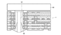
図1は、本発明の第1の実施形態に係るプリント配線板の構造を示す断面図である。図1に示すように、第1の実施形態に係るプリント配線板1は、第1プリント配線基材10、第2プリント配線基材20、第3プリント配線基材30、第4プリント配線基材40及び第5プリント配線基材50を、熱圧着により一括積層した構造を備えている。
図3〜図5は、プリント配線板の製造工程を示すフローチャートである。図6〜図8は、プリント配線板を製造工程毎に示す断面図である。なお、図3及び図6は第1、第2、第4及び第5プリント配線基材10,20,40,50について、図4及び図7は第3プリント配線基材30について、図5及び図8プリント配線板の最終工程についてそれぞれの製造工程の詳細を示している。
図11は、本発明の第2の実施形態に係るプリント配線板の構造を示す断面図である。図12は、図11のC矢視図である。図11及び図12に示すように、第2の実施形態に係るプリント配線板1Aは、第1〜第5プリント配線基材10〜50における各ビア14〜54の構造が、第1の実施形態に係るものと相違している。
5 ビアホール
6 マスク材
7 導体層
8 ソルダーレジスト
9 接着層
10 第1プリント配線基材
11 第1樹脂基材
12 配線
13 ランド部
14 ビア
20 第2プリント配線基材
21 第2樹脂基材
22 配線
23 ランド部
24 ビア
30 第3プリント配線基材
31 第3樹脂基材
32 配線
32a めっき層
33a,33b ランド部
34 ビア
40 第4プリント配線基材
41 第4樹脂基材
42 配線
43 ランド部
44 ビア
50 第5プリント配線基材
51 第5樹脂基材
52 配線
53 ランド部
54 ビア
60 スルーホール
90 電子部品
91 リード
99 半田
Claims (2)
- 絶縁層の少なくとも一方の面にランド部が形成された複数のプリント配線基材を、各ランド部が積層方向に沿って重なるように一括積層してなるプリント配線板であって、
前記複数のプリント配線基材の前記各ランド部の内側を前記積層方向に貫通するリード挿入用のスルーホールと、
前記複数のプリント配線基材に形成され、前記ランド部に接触すると共に前記スルーホールの周囲に配置された前記各プリント配線基材を貫通するビアと
を備え、
前記複数のプリント配線基材の一部は、片面に前記ランド部が形成された片面配線基材であり、
前記複数のプリント配線基材の他の一部は、両面に前記ランド部が形成された両面配線基材であり、
前記片面配線基材に形成されたビアは、導電ペーストからなる層間接続用のビアであり、
前記両面配線基材に形成されたビアは、両面に形成されたランド部を接続するめっきからなる導体間接続用のビアであり、
前記層間接続用のビアは、前記スルーホールの周囲に複数配置されると共に前記積層方向にスタック構造となるように配置され、
前記導体間接続用のビアは、前記スルーホールの周囲に複数配置されると共に前記積層方向から見て前記層間接続用のビアに対して前記スルーホールの周方向にずれるように配置されている
ことを特徴とするプリント配線板。 - 絶縁層の少なくとも一方の面にランド部が形成された複数のプリント配線基材を、各ランド部が積層方向に沿って重なるように一括積層してなるプリント配線板の製造方法であって、
前記絶縁層の一方の面に前記ランド部を形成し、他方の面側から前記ランド部に到達する開口部を前記ランド部の周囲に沿って形成した後、前記開口部内に導電ペーストを充填することにより層間接続用のビアを形成したプリント配線基材を製造する工程と、
前記絶縁層の両面における対応位置に前記ランド部をそれぞれ形成し、一方の面側のランド部から他方の面側のランド部に到達するように、又は前記両面のランド部を貫通するように開口部を前記ランド部の周囲に沿って形成した後、前記開口部内にめっきを施すことにより導体間接続用のビアを形成したプリント配線基材を製造する工程と、
複数の前記プリント配線基材を、各ランド部が前記積層方向に沿って重なるように一括積層する工程と、
前記複数のプリント配線基材の前記各ランド部の内側を前記積層方向に貫通するリード挿入用のスルーホールを、前記層間接続用及び前記導体間接続用のビアがその周囲に配置されるように形成する工程とを備え、
前記層間接続用及び前記導体間接続用のビアは、それぞれ前記ランド部の周囲に沿って複数形成され、
前記複数のプリント配線基材を一括積層する際に、前記層間接続用のビアが前記積層方向にスタック構造となるように配置すると共に、前記導体間接続用のビアが前記積層方向から見て前記層間接続用のビアに対してずれるように配置して積層する
ことを特徴とするプリント配線板の製造方法。
Priority Applications (1)
| Application Number | Priority Date | Filing Date | Title |
|---|---|---|---|
| JP2011281504A JP5765633B2 (ja) | 2011-12-22 | 2011-12-22 | プリント配線板及びその製造方法 |
Applications Claiming Priority (1)
| Application Number | Priority Date | Filing Date | Title |
|---|---|---|---|
| JP2011281504A JP5765633B2 (ja) | 2011-12-22 | 2011-12-22 | プリント配線板及びその製造方法 |
Publications (2)
| Publication Number | Publication Date |
|---|---|
| JP2013131687A JP2013131687A (ja) | 2013-07-04 |
| JP5765633B2 true JP5765633B2 (ja) | 2015-08-19 |
Family
ID=48909011
Family Applications (1)
| Application Number | Title | Priority Date | Filing Date |
|---|---|---|---|
| JP2011281504A Active JP5765633B2 (ja) | 2011-12-22 | 2011-12-22 | プリント配線板及びその製造方法 |
Country Status (1)
| Country | Link |
|---|---|
| JP (1) | JP5765633B2 (ja) |
Families Citing this family (1)
| Publication number | Priority date | Publication date | Assignee | Title |
|---|---|---|---|---|
| KR101883046B1 (ko) | 2016-04-15 | 2018-08-24 | 삼성전기주식회사 | 코일 전자 부품 |
Family Cites Families (4)
| Publication number | Priority date | Publication date | Assignee | Title |
|---|---|---|---|---|
| JPH1154934A (ja) * | 1997-06-06 | 1999-02-26 | Ibiden Co Ltd | 多層プリント配線板およびその製造方法 |
| JP3829660B2 (ja) * | 2000-12-14 | 2006-10-04 | 株式会社デンソー | プリント基板の実装構造およびプリント基板実装構造の製造方法 |
| KR100702554B1 (ko) * | 2002-05-23 | 2007-04-04 | 인터내셔널 비지네스 머신즈 코포레이션 | 다층 전자 장치 캐리어의 개량된 적층 비아 구조 |
| JP2004111701A (ja) * | 2002-09-19 | 2004-04-08 | Denso Corp | プリント配線板及びその製造方法 |
-
2011
- 2011-12-22 JP JP2011281504A patent/JP5765633B2/ja active Active
Also Published As
| Publication number | Publication date |
|---|---|
| JP2013131687A (ja) | 2013-07-04 |
Similar Documents
| Publication | Publication Date | Title |
|---|---|---|
| US8419884B2 (en) | Method for manufacturing multilayer wiring substrate | |
| JP3906225B2 (ja) | 回路基板、多層配線板、回路基板の製造方法および多層配線板の製造方法 | |
| JP5526276B1 (ja) | 部品内蔵基板及びその製造方法並びに実装体 | |
| JPWO2007046459A1 (ja) | 多層プリント配線基板及びその製造方法 | |
| JP5261756B1 (ja) | 多層配線基板 | |
| JP4110170B2 (ja) | 多層基板およびその製造方法 | |
| US9699921B2 (en) | Multi-layer wiring board | |
| JP2013135113A (ja) | 部品内蔵基板の製造方法 | |
| US20090071603A1 (en) | Method of manufacturing printed circuit board and electromagnetic bandgap structure | |
| JP5765633B2 (ja) | プリント配線板及びその製造方法 | |
| TW202339570A (zh) | 多層基板、多層基板的製造方法及電子機器 | |
| JP2014204088A (ja) | 多層配線基板およびその製造方法 | |
| JP6315681B2 (ja) | 部品内蔵基板及びその製造方法並びに実装体 | |
| JP6062884B2 (ja) | 部品内蔵基板及びその製造方法並びに実装体 | |
| JP5439165B2 (ja) | 多層配線板及びその製造方法 | |
| JP5836019B2 (ja) | 部品内蔵基板およびその製造方法 | |
| JP5408754B1 (ja) | 多層配線基板及びその製造方法 | |
| JP4292905B2 (ja) | 回路基板、多層基板、回路基板の製造方法および多層基板の製造方法 | |
| JP5906520B2 (ja) | 電子部品の製造方法及び電子部品内蔵プリント回路基板の製造方法 | |
| US11910540B2 (en) | Circuit board with solder mask on internal copper pad | |
| JP4899409B2 (ja) | 多層プリント配線基板及びその製造方法 | |
| JP2014027083A (ja) | 多層プリント配線基板 | |
| JP2005109188A (ja) | 回路基板、多層基板、回路基板の製造方法および多層基板の製造方法 | |
| JP4736251B2 (ja) | フィルムキャリア及びその製造方法 | |
| JP6020943B2 (ja) | 部品内蔵基板の製造方法 |
Legal Events
| Date | Code | Title | Description |
|---|---|---|---|
| A621 | Written request for application examination |
Free format text: JAPANESE INTERMEDIATE CODE: A621 Effective date: 20140606 |
|
| A977 | Report on retrieval |
Free format text: JAPANESE INTERMEDIATE CODE: A971007 Effective date: 20150115 |
|
| A131 | Notification of reasons for refusal |
Free format text: JAPANESE INTERMEDIATE CODE: A131 Effective date: 20150203 |
|
| A521 | Request for written amendment filed |
Free format text: JAPANESE INTERMEDIATE CODE: A523 Effective date: 20150326 |
|
| TRDD | Decision of grant or rejection written | ||
| A01 | Written decision to grant a patent or to grant a registration (utility model) |
Free format text: JAPANESE INTERMEDIATE CODE: A01 Effective date: 20150519 |
|
| A61 | First payment of annual fees (during grant procedure) |
Free format text: JAPANESE INTERMEDIATE CODE: A61 Effective date: 20150604 |
|
| R150 | Certificate of patent or registration of utility model |
Ref document number: 5765633 Country of ref document: JP Free format text: JAPANESE INTERMEDIATE CODE: R150 |
|
| R250 | Receipt of annual fees |
Free format text: JAPANESE INTERMEDIATE CODE: R250 |
|
| R250 | Receipt of annual fees |
Free format text: JAPANESE INTERMEDIATE CODE: R250 |
|
| R250 | Receipt of annual fees |
Free format text: JAPANESE INTERMEDIATE CODE: R250 |
|
| R250 | Receipt of annual fees |
Free format text: JAPANESE INTERMEDIATE CODE: R250 |
|
| R250 | Receipt of annual fees |
Free format text: JAPANESE INTERMEDIATE CODE: R250 |
|
| R250 | Receipt of annual fees |
Free format text: JAPANESE INTERMEDIATE CODE: R250 |
|
| R250 | Receipt of annual fees |
Free format text: JAPANESE INTERMEDIATE CODE: R250 |