JP5765633B2 - Printed wiring board and manufacturing method thereof - Google Patents
Printed wiring board and manufacturing method thereof Download PDFInfo
- Publication number
- JP5765633B2 JP5765633B2 JP2011281504A JP2011281504A JP5765633B2 JP 5765633 B2 JP5765633 B2 JP 5765633B2 JP 2011281504 A JP2011281504 A JP 2011281504A JP 2011281504 A JP2011281504 A JP 2011281504A JP 5765633 B2 JP5765633 B2 JP 5765633B2
- Authority
- JP
- Japan
- Prior art keywords
- printed wiring
- land
- vias
- wiring board
- land portion
- Prior art date
- Legal status (The legal status is an assumption and is not a legal conclusion. Google has not performed a legal analysis and makes no representation as to the accuracy of the status listed.)
- Active
Links
- 238000004519 manufacturing process Methods 0.000 title claims description 27
- 239000000758 substrate Substances 0.000 claims description 53
- 239000000463 material Substances 0.000 claims description 40
- 239000004020 conductor Substances 0.000 claims description 33
- 239000010410 layer Substances 0.000 claims description 29
- 239000011229 interlayer Substances 0.000 claims description 28
- 238000000034 method Methods 0.000 claims description 23
- 238000007747 plating Methods 0.000 claims description 21
- 238000010030 laminating Methods 0.000 claims description 14
- 230000000149 penetrating effect Effects 0.000 claims description 5
- 239000011347 resin Substances 0.000 description 32
- 229920005989 resin Polymers 0.000 description 32
- 239000000853 adhesive Substances 0.000 description 10
- 230000001070 adhesive effect Effects 0.000 description 10
- RYGMFSIKBFXOCR-UHFFFAOYSA-N Copper Chemical compound [Cu] RYGMFSIKBFXOCR-UHFFFAOYSA-N 0.000 description 9
- 239000012790 adhesive layer Substances 0.000 description 8
- PXHVJJICTQNCMI-UHFFFAOYSA-N Nickel Chemical compound [Ni] PXHVJJICTQNCMI-UHFFFAOYSA-N 0.000 description 6
- 229910000679 solder Inorganic materials 0.000 description 6
- 229910052802 copper Inorganic materials 0.000 description 5
- 239000010949 copper Substances 0.000 description 5
- 238000003475 lamination Methods 0.000 description 5
- 229920001721 polyimide Polymers 0.000 description 5
- 239000004593 Epoxy Substances 0.000 description 4
- 239000011889 copper foil Substances 0.000 description 4
- 238000005530 etching Methods 0.000 description 4
- 239000002923 metal particle Substances 0.000 description 4
- 239000011230 binding agent Substances 0.000 description 3
- 229910000765 intermetallic Inorganic materials 0.000 description 3
- 229910052759 nickel Inorganic materials 0.000 description 3
- 229910052709 silver Inorganic materials 0.000 description 3
- 239000004332 silver Substances 0.000 description 3
- 229920001187 thermosetting polymer Polymers 0.000 description 3
- XKRFYHLGVUSROY-UHFFFAOYSA-N Argon Chemical compound [Ar] XKRFYHLGVUSROY-UHFFFAOYSA-N 0.000 description 2
- CURLTUGMZLYLDI-UHFFFAOYSA-N Carbon dioxide Chemical compound O=C=O CURLTUGMZLYLDI-UHFFFAOYSA-N 0.000 description 2
- XEEYBQQBJWHFJM-UHFFFAOYSA-N Iron Chemical compound [Fe] XEEYBQQBJWHFJM-UHFFFAOYSA-N 0.000 description 2
- 229920000106 Liquid crystal polymer Polymers 0.000 description 2
- 239000004977 Liquid-crystal polymers (LCPs) Substances 0.000 description 2
- 239000004642 Polyimide Substances 0.000 description 2
- BQCADISMDOOEFD-UHFFFAOYSA-N Silver Chemical compound [Ag] BQCADISMDOOEFD-UHFFFAOYSA-N 0.000 description 2
- 239000003522 acrylic cement Substances 0.000 description 2
- 229910045601 alloy Inorganic materials 0.000 description 2
- 239000000956 alloy Substances 0.000 description 2
- 238000005266 casting Methods 0.000 description 2
- ORTQZVOHEJQUHG-UHFFFAOYSA-L copper(II) chloride Chemical compound Cl[Cu]Cl ORTQZVOHEJQUHG-UHFFFAOYSA-L 0.000 description 2
- 230000000694 effects Effects 0.000 description 2
- 239000007789 gas Substances 0.000 description 2
- PCHJSUWPFVWCPO-UHFFFAOYSA-N gold Chemical compound [Au] PCHJSUWPFVWCPO-UHFFFAOYSA-N 0.000 description 2
- 229910052737 gold Inorganic materials 0.000 description 2
- 239000010931 gold Substances 0.000 description 2
- 238000002844 melting Methods 0.000 description 2
- 230000008018 melting Effects 0.000 description 2
- 239000002985 plastic film Substances 0.000 description 2
- 229920006255 plastic film Polymers 0.000 description 2
- 229920006259 thermoplastic polyimide Polymers 0.000 description 2
- 239000002966 varnish Substances 0.000 description 2
- JOYRKODLDBILNP-UHFFFAOYSA-N Ethyl urethane Chemical compound CCOC(N)=O JOYRKODLDBILNP-UHFFFAOYSA-N 0.000 description 1
- 229910021578 Iron(III) chloride Inorganic materials 0.000 description 1
- ATJFFYVFTNAWJD-UHFFFAOYSA-N Tin Chemical compound [Sn] ATJFFYVFTNAWJD-UHFFFAOYSA-N 0.000 description 1
- NIXOWILDQLNWCW-UHFFFAOYSA-N acrylic acid group Chemical group C(C=C)(=O)O NIXOWILDQLNWCW-UHFFFAOYSA-N 0.000 description 1
- 239000000654 additive Substances 0.000 description 1
- 229910052782 aluminium Inorganic materials 0.000 description 1
- XAGFODPZIPBFFR-UHFFFAOYSA-N aluminium Chemical compound [Al] XAGFODPZIPBFFR-UHFFFAOYSA-N 0.000 description 1
- 229910052786 argon Inorganic materials 0.000 description 1
- QVGXLLKOCUKJST-UHFFFAOYSA-N atomic oxygen Chemical compound [O] QVGXLLKOCUKJST-UHFFFAOYSA-N 0.000 description 1
- 230000015572 biosynthetic process Effects 0.000 description 1
- 229910052797 bismuth Inorganic materials 0.000 description 1
- JCXGWMGPZLAOME-UHFFFAOYSA-N bismuth atom Chemical compound [Bi] JCXGWMGPZLAOME-UHFFFAOYSA-N 0.000 description 1
- 229910002092 carbon dioxide Inorganic materials 0.000 description 1
- 239000001569 carbon dioxide Substances 0.000 description 1
- 238000003486 chemical etching Methods 0.000 description 1
- 239000011248 coating agent Substances 0.000 description 1
- 238000000576 coating method Methods 0.000 description 1
- 229960003280 cupric chloride Drugs 0.000 description 1
- 238000005553 drilling Methods 0.000 description 1
- 239000003822 epoxy resin Substances 0.000 description 1
- 239000000945 filler Substances 0.000 description 1
- 229910052738 indium Inorganic materials 0.000 description 1
- APFVFJFRJDLVQX-UHFFFAOYSA-N indium atom Chemical compound [In] APFVFJFRJDLVQX-UHFFFAOYSA-N 0.000 description 1
- 239000011261 inert gas Substances 0.000 description 1
- 238000003780 insertion Methods 0.000 description 1
- 230000037431 insertion Effects 0.000 description 1
- 229910052742 iron Inorganic materials 0.000 description 1
- RBTARNINKXHZNM-UHFFFAOYSA-K iron trichloride Chemical compound Cl[Fe](Cl)Cl RBTARNINKXHZNM-UHFFFAOYSA-K 0.000 description 1
- 229910052751 metal Inorganic materials 0.000 description 1
- 239000002184 metal Substances 0.000 description 1
- 239000001301 oxygen Substances 0.000 description 1
- 229910052760 oxygen Inorganic materials 0.000 description 1
- 239000002245 particle Substances 0.000 description 1
- 238000000059 patterning Methods 0.000 description 1
- 238000000206 photolithography Methods 0.000 description 1
- 229920000647 polyepoxide Polymers 0.000 description 1
- 239000009719 polyimide resin Substances 0.000 description 1
- 229920000098 polyolefin Polymers 0.000 description 1
- 238000003825 pressing Methods 0.000 description 1
- 238000007639 printing Methods 0.000 description 1
- 238000003672 processing method Methods 0.000 description 1
- 238000007650 screen-printing Methods 0.000 description 1
- 238000005476 soldering Methods 0.000 description 1
- 238000004528 spin coating Methods 0.000 description 1
- 238000005507 spraying Methods 0.000 description 1
- 238000004544 sputter deposition Methods 0.000 description 1
- 239000000126 substance Substances 0.000 description 1
- TXEYQDLBPFQVAA-UHFFFAOYSA-N tetrafluoromethane Chemical compound FC(F)(F)F TXEYQDLBPFQVAA-UHFFFAOYSA-N 0.000 description 1
- 229920001169 thermoplastic Polymers 0.000 description 1
- 239000004416 thermosoftening plastic Substances 0.000 description 1
- 229910052718 tin Inorganic materials 0.000 description 1
- 238000009281 ultraviolet germicidal irradiation Methods 0.000 description 1
Images


Landscapes
- Production Of Multi-Layered Print Wiring Board (AREA)
Description
この発明は、電子部品に接続されたリード(端子)をスルーホールに挿入して半田付けするプリント配線板及びその製造方法に関する。 The present invention relates to a printed wiring board in which a lead (terminal) connected to an electronic component is inserted into a through hole and soldered, and a manufacturing method thereof.
近年、携帯電話やデジタルスチルカメラ(DSC)等のデジタル機器の小型化や薄型化に伴い、これらに用いられる電子部品が実装されるランド部を有するプリント配線板についても、同様に小型で薄いものが求められている。このようなプリント配線板としては、例えば特許文献1に示すような電子部品のリードを挿入するスルーホールが形成されたタイプのものが知られている。この種のプリント配線板のスルーホールには、プリント配線板の電子部品のリード先端部が半田付けされる裏面から表面への電気的導通を図るためにめっき処理が施される。
In recent years, with the miniaturization and thinning of digital devices such as mobile phones and digital still cameras (DSCs), printed wiring boards having land portions on which electronic components used in these devices are mounted are similarly small and thin. Is required. As such a printed wiring board, for example, a type in which a through hole for inserting a lead of an electronic component as shown in
しかしながら、上記特許文献1に開示された従来技術のプリント配線板のように、スルーホールにめっきを施したものの場合、積層数が増えて配線板の厚みが厚くなると、スルーホールのめっき部分のアスペクト比が高くなる。この場合、応力が加わることでスルーホール内のめっきに亀裂等が生じ易くなり、電気的接続信頼性が低下するという問題がある。また、信頼性を向上させるためには、めっき厚を厚くしなければならず、コストアップにつながってしまう。
However, in the case where the through hole is plated, such as the conventional printed wiring board disclosed in
この発明は、上述した従来技術による問題点を解消し、電気的接続信頼性を確保することができるプリント配線板及びその製造方法を提供することを目的とする。 SUMMARY OF THE INVENTION An object of the present invention is to provide a printed wiring board that can solve the above-described problems caused by the prior art and ensure electrical connection reliability, and a method for manufacturing the same.
本発明に係るプリント配線板は、絶縁層の少なくとも一方の面にランド部が形成された複数のプリント配線基材を、各ランド部が積層方向に沿って重なるように一括積層してなるプリント配線板であって、前記複数のプリント配線基材の前記各ランド部の内側を前記積層方向に貫通するリード挿入用のスルーホールと、前記複数のプリント配線基材に形成され、前記ランド部に接触すると共に前記スルーホールの周囲に配置された前記各プリント配線基材を貫通するビアとを備えたことを特徴とする。 The printed wiring board according to the present invention comprises a plurality of printed wiring substrates having land portions formed on at least one surface of an insulating layer, and a plurality of printed wiring substrates laminated in a lump so that the land portions overlap in the stacking direction. A plurality of printed wiring bases formed in the plurality of printed wiring bases and in contact with the land parts, and through holes for inserting leads that penetrate the inner sides of the land parts of the plurality of printed wiring bases in the stacking direction. And a via penetrating each printed wiring board disposed around the through hole.
本発明によれば、電子部品のリード挿入用のスルーホールの周囲にランド部に接触すると共に各プリント配線基材を貫通するビアが配置されているので、これらビアを介してスルーホールの両側の電気的接続が図れ、スルーホールにめっきを施す必要がない。また、各ビアのいずれかに亀裂等が生じてもスルーホールにめっきを施した場合と比べて電気的接続信頼性が低下することはない。このため、電気的接続信頼性を確保することが可能となる。 According to the present invention, the vias that contact the land portion and penetrate the printed wiring boards are disposed around the through hole for inserting the lead of the electronic component. Electrical connection can be achieved, and there is no need to plate through holes. Further, even if a crack or the like occurs in any of the vias, the electrical connection reliability is not lowered as compared with the case where the through hole is plated. For this reason, it becomes possible to ensure electrical connection reliability.
本発明の一実施形態においては、前記複数のプリント配線基材の一部が、片面に前記ランド部が形成された片面配線基材であり、前記複数のプリント配線基材の他の一部が、両面に前記ランド部が形成された両面配線基材であり、前記片面配線基材に形成されたビアが、導電ペーストからなる層間接続用のビアであり、前記両面配線基材に形成されたビアが、両面に形成されたランド部を接続するめっきからなる導体間接続用のビアである。 In one embodiment of the present invention, a part of the plurality of printed wiring substrates is a single-sided wiring substrate in which the land portion is formed on one side, and the other part of the plurality of printed wiring substrates is The double-sided wiring base material in which the land portions are formed on both sides, and the via formed in the single-sided wiring base material is an interlayer connection via made of a conductive paste, and is formed in the double-sided wiring base material. The via is a via for conductor connection made of plating for connecting the land portions formed on both surfaces.
この場合、前記層間接続用のビアは、前記スルーホールの周囲に複数配置されると共に前記積層方向にスタック構造となるように配置され、前記導体間接続用のビアは、前記スルーホールの周囲に複数配置されると共に前記積層方向から見て前記層間接続用のビアに対して前記スルーホールの周方向にずれるように配置されていることが望ましい。 In this case, a plurality of the vias for interlayer connection are arranged around the through hole and arranged in a stack structure in the stacking direction, and the vias for connecting the conductors are arranged around the through hole. It is desirable that a plurality of them are arranged and arranged so as to be shifted in the circumferential direction of the through hole with respect to the interlayer connection via as viewed from the stacking direction.
本発明に係るプリント配線板の製造方法は、絶縁層の少なくとも一方の面にランド部が形成された複数のプリント配線基材を、各ランド部が積層方向に沿って重なるように一括積層してなるプリント配線板の製造方法であって、前記絶縁層の一方の面に前記ランド部を形成し、他方の面側から前記ランド部に到達する開口部を前記ランド部の周囲に沿って形成した後、前記開口部内に導電ペーストを充填することにより層間接続用のビアを形成したプリント配線基材を製造する工程と、前記絶縁層の両面における対応位置に前記ランド部をそれぞれ形成し、一方の面側のランド部から他方の面側のランド部に到達するように、又は前記両面のランド部を貫通するように開口部を前記ランド部の周囲に沿って形成した後、前記開口部内にめっきを施すことにより導体間接続用のビアを形成したプリント配線基材を製造する工程と、複数の前記プリント配線基材を、各ランド部が前記積層方向に沿って重なるように一括積層する工程と、前記複数のプリント配線基材の前記各ランド部の内側を前記積層方向に貫通するリード挿入用のスルーホールを、前記層間接続用及び前記導体間接続用のビアがその周囲に配置されるように形成する工程とを備えたことを特徴とする。 The method for manufacturing a printed wiring board according to the present invention includes laminating a plurality of printed wiring base materials having land portions formed on at least one surface of an insulating layer so that the land portions overlap each other in the stacking direction. In the printed wiring board manufacturing method, the land portion is formed on one surface of the insulating layer, and an opening reaching the land portion from the other surface side is formed along the periphery of the land portion. Thereafter, a step of manufacturing a printed wiring board in which vias for interlayer connection are formed by filling the openings with a conductive paste, and forming the land portions at corresponding positions on both surfaces of the insulating layer, After the opening is formed along the periphery of the land portion so as to reach the land portion on the other surface side from the land portion on the surface side, or through the land portions on both surfaces, plating is performed in the opening portion. A step of producing a printed wiring substrate in which vias for connecting conductors are formed by applying, a step of laminating a plurality of the printed wiring substrates together so that each land portion overlaps along the laminating direction, A through hole for inserting a lead that penetrates the inside of each land portion of the plurality of printed wiring substrates in the stacking direction, and a via for connecting the interlayer and connecting between the conductors are arranged around the via hole. And a forming step.
本発明によれば、複数のプリント配線基材の一括積層後に形成された電子部品のリード挿入用のスルーホールの周囲に、層間接続用及び導体間接続用のビアが配置されるので、配線板の表裏接続のためにスルーホールにめっきを施す工程が不要となる。また、各ビアのいずれかに亀裂等が生じても電気的接続信頼性が低下することはない。このため、製造工程数を増やさずに、電気的接続信頼性を向上させることができるプリント配線板を製造可能となる。 According to the present invention, vias for inter-layer connection and inter-conductor connection are arranged around through holes for lead insertion of electronic parts formed after batch lamination of a plurality of printed wiring substrates. The process of plating the through-hole for the front and back connection is not required. Further, even if a crack or the like occurs in any of the vias, the electrical connection reliability does not decrease. For this reason, it becomes possible to manufacture a printed wiring board capable of improving the electrical connection reliability without increasing the number of manufacturing steps.
本発明の一実施形態においては、前記層間接続用及び前記導体間接続用のビアは、それぞれ前記ランド部の周囲に沿って複数形成され、前記複数のプリント配線基材を一括積層する際に、前記層間接続用のビアが前記積層方向にスタック構造となるように配置すると共に、前記導体間接続用のビアが前記積層方向から見て前記層間接続用のビアに対してずれるように配置して積層する。 In one embodiment of the present invention, a plurality of the vias for interlayer connection and the connection between conductors are respectively formed along the periphery of the land portion, and when laminating the plurality of printed wiring substrates together, The inter-layer connection vias are arranged so as to form a stack structure in the stacking direction, and the inter-conductor connection vias are arranged so as to be shifted from the inter-layer connection vias when viewed from the stacking direction. Laminate.
本発明によれば、電気的接続信頼性を確保することができる。 According to the present invention, electrical connection reliability can be ensured.
以下、添付の図面を参照して、この発明の実施の形態に係るプリント配線板及びその製造方法を詳細に説明する。 Hereinafter, a printed wiring board and a manufacturing method thereof according to embodiments of the present invention will be described in detail with reference to the accompanying drawings.
[第1の実施形態]
図1は、本発明の第1の実施形態に係るプリント配線板の構造を示す断面図である。図1に示すように、第1の実施形態に係るプリント配線板1は、第1プリント配線基材10、第2プリント配線基材20、第3プリント配線基材30、第4プリント配線基材40及び第5プリント配線基材50を、熱圧着により一括積層した構造を備えている。
[First Embodiment]
FIG. 1 is a sectional view showing the structure of a printed wiring board according to the first embodiment of the present invention. As shown in FIG. 1, the printed
また、プリント配線板1には、第1〜第5プリント配線基材10〜50を積層方向に貫通するスルーホール60が形成されている。このスルーホール60には、プリント配線板1に実装される、後述する電子部品のリード(端子)が挿入される。スルーホール60は、例えば半径(φ1/2)が約500μm程度となるように、レーザ加工、金型加工又はドリル加工などで形成される。
Further, the printed
第1〜第5プリント配線基材10〜50は、それぞれ絶縁層としての第1樹脂基材11、第2樹脂基材21、第3樹脂基材31、第4樹脂基材41及び第5樹脂基材51と、これら第1〜第5プリント配線基材10〜50の少なくとも一方の面(片面)に形成された配線12,22,32,42,52とを備える。
The 1st-5th printed wiring base materials 10-50 are the 1st
また、第1〜第5プリント配線基材10〜50は、それぞれ第1、第2、第4及び第5樹脂基材11,21,41,51の片面に形成されたランド部13,23,43,53と、第3樹脂基材31の両面における対応位置に形成されたランド部33a,33bとを備える。従って、第3プリント配線基材30は、いわゆるコア基板である両面板(両面CCL)からなり、これ以外は片面板(片面CCL)からなる。プリント配線板1は、各プリント配線基材10〜50を、各ランド部13〜53が積層方向に沿って重なるように一括積層してなる。
Further, the first to fifth printed
第1、第2、第4及び第5プリント配線基材10,20,40,50は、例えばスルーホール60の周囲に配置されるように形成されたビアホール内に導電ペーストを充填して形成され、ランド部13,23,43,53と接触して電気的に接続される複数の層間接続用のビア14,24,44,54を備える。また、第3プリント配線基材30は、例えばスルーホール60の周囲に配置されるように形成されたビアホール内にめっき形成され、各ランド部33a,33bに接触して電気的に接続される複数の導体間接続用のビア34を備える。
The first, second, fourth, and fifth printed
なお、ビア34は、例えば一方のランド部33aを貫通させることなく、他方のランド部33b側から形成したビアホール(貫通孔)内にめっきを施した構造のLVHのめっきビアからなり、例えば銅めっきにより形成される。この場合、ランド部33aや配線32上にはめっき層32aが形成される。
The
また、ビア34は、ビアホール内をめっきする代わりに導電ペーストを充填させる構造としてもよい。その他、ビア34は、図示は省略するが、各ランド部33a,33b間を貫通するスルーホール(貫通孔)内にめっきを施した構造のIVHのめっきスルーホールにより構成されてもよい。
The via 34 may have a structure in which a conductive paste is filled instead of plating in the via hole. In addition, although illustration is abbreviate | omitted, the via | veer 34 may be comprised by the plated through hole of IVH of the structure which plated in the through hole (through-hole) which penetrates between each
ビア14〜54は、図2に示すように、スルーホール60の周囲に複数配置されると共に各プリント配線基材10〜50の積層方向にスタック構造となるように配置される。一方、ビア34は、同様にスルーホール60の周囲に複数配置されるが、上記積層方向から見て各ビア14〜54に対してスルーホール60の周方向に、例えばスルーホール60の中心に対して45°ずつずれるように配置されている。
As shown in FIG. 2, a plurality of
従って、図1においては断面構造を図示する便宜上、ビア34が他のビア14,24,44,54と同一断面上に配置されているかのように記載してあるが、実際にはそれぞれずれて配置されている。このため、ビア34の凹み部分には、一括積層時に層間接着のための接着層9が流入する。なお、これら各ビア14〜54の直径φ2は、上述したような加工法により約100μm程度となるように形成されている。
Therefore, in FIG. 1, for convenience of illustrating the cross-sectional structure, the via 34 is described as if it is disposed on the same cross section as the
このように、ビア34を他のビア14,24,44,54に対してずれるように配置することにより、積層時の加圧圧力がビア34の凹み部分に作用してビア34が潰れ、各ビア14〜54に対して加圧圧力が不足することを防止し、確実に各ランド部13〜53間を層間接続することが可能となる。なお、ビア34をずらさずにスタック構造となるように配置する場合は、このビア34の凹み部分に十分充填されるように、ビア44のめっき又は導電ペースト量を設定する必要がある。
Thus, by arranging the via 34 so as to be displaced with respect to the
第1〜第5樹脂基材11〜51は、樹脂フィルムにより構成されている。樹脂フィルムとしては、例えば熱可塑性のポリイミド、ポリオレフィン、液晶ポリマーなどからなる樹脂フィルムや、熱硬化性のエポキシ樹脂、ポリイミド樹脂からなる樹脂フィルムなどを用いることができる。 The 1st-5th resin base materials 11-51 are comprised by the resin film. As the resin film, for example, a resin film made of thermoplastic polyimide, polyolefin, liquid crystal polymer or the like, a resin film made of thermosetting epoxy resin, polyimide resin, or the like can be used.
なお、配線12〜52やランド部13〜53は、例えば銅箔などの導電材をパターン形成してなる。また、導電ペーストは、例えばニッケル、金、銀、銅、アルミニウム、鉄などから選択される少なくとも1種類の低電気抵抗の金属粒子と、錫、ビスマス、インジウム、鉛などから選択される少なくとも1種類の低融点の金属粒子とを含み、エポキシ、アクリル、ウレタンなどを主成分とするバインダ成分を混合したペーストからなる。
The
このように構成された導電ペーストは、含有された低融点の金属が200℃以下で溶融し合金を形成することができ、特に銅や銀などとは金属間化合物を形成することができる特性を備える。従って、各ビア14,24,44,54と各ランド部13,23,43,53(めっき層32aを含む)との接続部は、一括積層時に金属間化合物により合金化される。なお、導電ペーストは、例えば粒子径がナノレベルの金、銀、銅、ニッケル等のフィラーが、上記のようなバインダ成分に混合されたナノペーストで構成することもできる。
The conductive paste thus configured has a characteristic that the contained low melting point metal can be melted at 200 ° C. or less to form an alloy, and in particular, can form an intermetallic compound with copper or silver. Prepare. Therefore, the connection portions between the vias 14, 24, 44, 54 and the
その他、導電ペーストは、上記ニッケル等の金属粒子が、上記のようなバインダ成分に混合されたペーストで構成することもできる。この場合、導電ペーストは、金属粒子同士が接触することで電気的接続が行われる特性となる。導電ペーストのビアホールへの充填方法としては、例えば印刷法、スピン塗布工法、スプレー塗布工法、ディスペンス工法、ラミネート工法、及びこれらを併用した工法などを用いることができる。 In addition, the conductive paste can also be composed of a paste in which metal particles such as nickel are mixed with the binder component as described above. In this case, the conductive paste has a characteristic that electrical connection is made when metal particles come into contact with each other. As a method for filling the via hole with the conductive paste, for example, a printing method, a spin coating method, a spray coating method, a dispensing method, a laminating method, and a method using these in combination can be used.
接着層9を介して積層された各プリント配線基材10〜50のうち、最表層に配置されるプリント配線基材10,50の表面は、露出する配線やランド部を除いてソルダーレジスト8により覆われている。接着層9は、例えばエポキシ系やアクリル系の接着剤など、揮発成分が含まれた有機系接着剤などからなる。
Of the printed
このように構成されたプリント配線板1は、導電ペーストからなる層間接続用のビア14,24,44,54及び導体間接続用のビア34が複数形成されているので、例えばいずれかに亀裂等が生じても他のビアで最表層の表面間の電気的導通をとることができる。これにより、電気的接続信頼性を確保することができる。
Since the printed
また、各ビア14〜54で電気的導通をとっているので、スルーホール60の部分の導通をとる必要がない。このため、プリント配線基材10〜50の積層後に、プリント配線板1の表裏接続のためにスルーホール60に別途めっきを施す必要がなく、その分の製造工程数やめっき材料を削減して、コストの低減を図ることができる。
Further, since each via 14 to 54 is electrically connected, it is not necessary to conduct the portion of the through
次に、第1の実施形態に係るプリント配線板1の製造方法について説明する。
図3〜図5は、プリント配線板の製造工程を示すフローチャートである。図6〜図8は、プリント配線板を製造工程毎に示す断面図である。なお、図3及び図6は第1、第2、第4及び第5プリント配線基材10,20,40,50について、図4及び図7は第3プリント配線基材30について、図5及び図8プリント配線板の最終工程についてそれぞれの製造工程の詳細を示している。
Next, a method for manufacturing the printed
3-5 is a flowchart which shows the manufacturing process of a printed wiring board. 6-8 is sectional drawing which shows a printed wiring board for every manufacturing process. 3 and 6 show the first, second, fourth, and fifth printed
まず、図3を参照しながら、第1、第2、第4及び第5プリント配線基材10,20,40,50の製造工程について説明する。なお、これらは同様の工程で製造することができるので、ここでは代表して第1プリント配線基材10の製造工程について説明するが、第2、第4及び第5プリント配線基材20,40,50についても同様である。
First, the manufacturing process of the first, second, fourth, and fifth printed
図6(a)に示すように、第1樹脂基材11の一方の面に導体層7が形成された片面銅張積層板(片面CCL)を準備する(ステップS100)。次に、導体層7上にフォトリソグラフィによりエッチングレジストを形成した後にエッチングを行って、図6(b)に示すように、配線12及びランド部13等の導体パターンを形成する(ステップS102)。
As shown in FIG. 6A, a single-sided copper-clad laminate (single-sided CCL) in which the
ステップS100にて使用する片面CCLは、例えば厚さ12μmの銅箔からなる導体層7に、厚さ25μm程度の第1樹脂基材11を貼り合わせた構造からなる。なお、この片面CCLとしては、例えばキャスティング法により、銅箔にポリイミドのワニスを塗布してそのワニスを硬化させて作製されたものを使用することができる。
The single-sided CCL used in step S100 has a structure in which the first
キャスティング法は、押出機によって溶融された樹脂を、平坦なダイに設けられた直線状のスリットから押し出して、その溶融膜を冷却されたロールで急速に冷やして圧延しながら巻き取ることで、平坦なフィルムやシートを成形する公知の方法である。この方法は信頼性が高く多用されている。 In the casting method, the resin melted by the extruder is extruded from a linear slit provided on a flat die, and the molten film is rapidly cooled with a cooled roll and rolled up while being rolled. It is a known method for forming a simple film or sheet. This method is highly reliable and widely used.
その他、片面CCLとしては、ポリイミドフィルム上にシード層をスパッタリングにより形成し、めっきにより銅を成長させて導体層7を形成したものや、圧延或いは電解銅箔とポリイミドフィルムとを接着材により貼り合わせて作製されたものなどを使用することもできる。なお、第1樹脂基材11は必ずしもポリイミドからなるものである必要はなく、上記のように液晶ポリマー等のプラスチックフィルムからなるものであってもよい。また、ステップS102でのエッチングには塩化第二鉄を主成分とするエッチャントや、塩化第二銅を主成分とするエッチャントなどを用いることができる。上記はサブトラクティブ法を用いて回路形成する説明を行ったが、セミアディティブ法を用いて回路形成をしてもよい。
In addition, as single-sided CCL, a seed layer is formed on a polyimide film by sputtering, copper is grown by plating, and a
導体パターンを形成したら、図6(c)に示すように、第1樹脂基材11の配線12及びランド部13形成面側と反対側の面に、接着材9a及びマスク材6を加熱圧着により貼り付ける(ステップS104)。このステップS104にて貼り付けられる接着材9aとしては、例えば厚さ25μm程度のエポキシ系熱硬化性フィルムを使用することができる。加熱圧着には真空ラミネータを用い、減圧下の雰囲気中にて、接着材9aの硬化温度以下の温度で0.3MPaの圧力によりプレスしてこれらを貼り合わせることが挙げられる。
When the conductor pattern is formed, as shown in FIG. 6C, the adhesive 9a and the
なお、接着層9を構成する接着材9aに用いられる層間接着材は、エポキシ系の熱硬化性フィルムのみならず、アクリル系の接着材や、熱可塑性ポリイミドなどに代表される熱可塑性接着材などが挙げられる。また、層間接着材は必ずしもフィルム状である必要はなく、ワニス状の樹脂を塗布したものであってもよい。マスク材6は、上述した樹脂フィルムやPET,PENなどのプラスチックフィルムの他、UV照射によって接着や剥離が可能な各種フィルムを用いることができる。
The interlayer adhesive used for the adhesive 9a constituting the
そして、図6(d)に示すように、貼り付けたマスク材6側から、ランド部13の周囲に沿ってマスク材6、接着材9a及び第1樹脂基材11を貫通するビアホール5を所定箇所に複数形成し(ステップS106)、ビアホール5内に例えばプラズマデスミア処理を施す。
Then, as shown in FIG. 6D, via
ステップS106にて形成されるビアホール5は、上述したように直径φ100μm程度であり、例えばUVレーザを使用して所定箇所に複数形成される。ビアホール5は、その他、炭酸ガスレーザやエキシマレーザなどで形成してもよいし、ドリル加工や化学的なエッチングなどにより形成してもよい。
As described above, the via
また、プラズマデスミア処理は、CF4及びO2(四フッ化メタン+酸素)の混合ガスにより行うことができるが、Ar(アルゴン)などのその他の不活性ガスを用いることもでき、いわゆるドライ処理ではなく、薬液を用いたウェットデスミア処理としてもよい。 The plasma desmear treatment can be performed with a mixed gas of CF 4 and O 2 (tetrafluoromethane + oxygen), but other inert gas such as Ar (argon) can also be used, so-called dry treatment. Instead, it may be wet desmear treatment using a chemical solution.
その後、図6(e)に示すように、形成したビアホール5内に、例えばスクリーン印刷により導電ペーストを充填して層間接続用のビア14を形成し(ステップS108)、図6(f)に示すように、マスク材6を剥離して除去し(ステップS110)、配線12及びランド部13が形成されると共に、接着層9が備えられた第1樹脂基材11を有する第1プリント配線基材10を形成する。このような処理を行って、第2、第4及び第5プリント配線基材20,40,50や、更に多層の場合はその他のプリント配線基材を形成して準備しておく。
After that, as shown in FIG. 6E, the via
次に、図4を参照しながら第3プリント配線基材30の製造工程について説明する。なお、既に説明した箇所には同一の符号を附して説明を割愛する場合があり、各ステップの具体的な処理内容については上述した内容を適用可能であるとする。まず、図7(a)に示すように、第3樹脂基材31の両面に導体層7が形成された両面銅張積層板(両面CCL)を準備し(ステップS200)、図7(b)に示すように、導体間接続が必要なランド部となる部分の周囲に沿った箇所やその他の所望箇所などの所定箇所であって、各ビア14,24,44,54とずれる位置にビアホール5を形成して(ステップS202)、例えばプラズマデスミア処理を行う。
Next, the manufacturing process of the third printed
次に、図7(c)に示すように、第3樹脂基材31の全面にパネルめっき処理を施して(ステップS204)、導体層7上及びビアホール5内にめっき層32aを形成する。なお、ビアホール5内のめっき層32aのうちの一部は、後に導体間接続用のビア34として用いられるめっきビアとなり、第3樹脂基材31の両面の導体層7を電気的に導通している。
Next, as shown in FIG. 7C, panel plating is performed on the entire surface of the third resin base material 31 (step S <b> 204) to form a
最後に、図7(d)に示すように、第3樹脂基材31の両面にエッチング等により配線32やランド部33a,33b、導体間接続用のビア34などの配線パターンを形成し(ステップS206)、第3プリント配線基材30を形成する。なお、ステップS202にてビアホール5を形成する代わりに、図示しないスルーホールを形成してステップS204にてめっき処理を施し、めっきスルーホールを導体間接続用のビア34として形成するようにしてもよい。
Finally, as shown in FIG. 7D, wiring patterns such as
次に、図5を参照しながら各プリント配線基材10〜50の積層工程以降の製造工程について説明する。上記のように、第1〜第5プリント配線基材10〜50を作製したら、図8(a)に示すように、各ランド部13〜53及び各ビア14〜54を、例えば電子部品用実装機で位置合わせする。このとき、上述したように、導体間接続用のビア34は各ビア14,24,44,54とずれるように位置合わせされる。
Next, the manufacturing process after the lamination process of each printed wiring base materials 10-50 is demonstrated, referring FIG. As described above, when the first to fifth printed
そして、図8(b)に示すように、第1、第2、第4及び第5プリント配線基材10,20,40,50の接着層9及び層間接続用のビア14,24,44,54の導電ペーストが硬化していない状態で、各プリント配線基材10〜50を仮固定する(ステップS300)。
Then, as shown in FIG. 8B, the
その後、各プリント配線基材10〜50を熱圧着して一括積層する(ステップS302)。このステップS302においては、例えば真空プレス機を用いて、1kPa以下の減圧雰囲気中にて加熱加圧することで熱圧着により一括積層し、図1に示すようなプリント配線板1を製造する。このとき、層間の各接着層9や各樹脂基材11等の硬化と同時に、ビアホール5に充填された導電ペーストの硬化及び合金化が行われる。従って、導電ペーストと接する各ランド部13等との間には、金属間化合物の合金層が形成される。
Thereafter, the printed
そして、図8(c)に示すように、プリント配線板1における最表層のプリント配線基材10,50のランド部13,53側の樹脂基材11,51上に、ソルダーレジスト8をパターン形成する(ステップS304)。なお、この時点でのプリント配線板1においては、図9に示すように、ランド部13等の周囲に、層間接続用のビア14,24,44,54と導体間接続用のビア34とがずれて配置されている。
And as shown in FIG.8 (c), solder resist 8 is pattern-formed on the
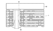
最後に、各ランド部13〜53の中心に、図1及び図2に示すようなスルーホール60を形成すれば(ステップS306)、スルーホール60の周囲にビア14〜54が配置された本実施形態に係るプリント配線板1が形成される。なお、図10に示すように、プリント配線板1に電子部品90を実装する場合は、例えば第1プリント配線基材10側から電子部品90のリード91をスルーホール60に挿入し、第5プリント配線基材50のランド部53とリード91とを半田99により接続して、電子部品90をプリント配線板1に実装する(ステップS308)。
Finally, if through
このように電子部品90を実装することができるので、上記作用効果のみならず、第1プリント配線基材10のランド部13側に半田付けを行う必要がなく、半田99の材料コストを抑えることができると共に、電気的接続信頼性を確保することができる。
Since the
[第2の実施形態]
図11は、本発明の第2の実施形態に係るプリント配線板の構造を示す断面図である。図12は、図11のC矢視図である。図11及び図12に示すように、第2の実施形態に係るプリント配線板1Aは、第1〜第5プリント配線基材10〜50における各ビア14〜54の構造が、第1の実施形態に係るものと相違している。
[Second Embodiment]
FIG. 11 is a cross-sectional view showing the structure of a printed wiring board according to the second embodiment of the present invention. 12 is a view taken in the direction of arrow C in FIG. As shown in FIGS. 11 and 12, the printed wiring board 1A according to the second embodiment has the structure of the vias 14 to 54 in the first to fifth printed
すなわち、層間接続用のビア14,24,44,54は、各ランド部13,23,43,53に対してそれぞれ大きく一つ形成されたビアホール内に充填形成され、導体間接続用のビア34は、これら各ビア14,24,44,54のビアホールと同等かそれ以上の大きさをもって形成されたビアホール内にめっき形成されている。
In other words, the
この場合、ビア34の凹み部分に対して確実に接続されるように、例えば層間接続用のビア44は他の層間接続用のビア14,24,54よりも高さ(厚さ)が高くなる(厚くなる)ように形成されている。そして、スルーホール60は、これら各ビア14〜54及び各ランド部13〜53を貫通するように形成される。このような構造によっても、上記第1の実施形態に係るプリント配線板1と同等の作用効果を奏することができる。
In this case, for example, the interlayer connection via 44 is higher in height (thickness) than the other interlayer connection vias 14, 24, and 54 so as to be reliably connected to the recessed portion of the via 34. It is formed to be thicker. The through
1,1A プリント配線板
5 ビアホール
6 マスク材
7 導体層
8 ソルダーレジスト
9 接着層
10 第1プリント配線基材
11 第1樹脂基材
12 配線
13 ランド部
14 ビア
20 第2プリント配線基材
21 第2樹脂基材
22 配線
23 ランド部
24 ビア
30 第3プリント配線基材
31 第3樹脂基材
32 配線
32a めっき層
33a,33b ランド部
34 ビア
40 第4プリント配線基材
41 第4樹脂基材
42 配線
43 ランド部
44 ビア
50 第5プリント配線基材
51 第5樹脂基材
52 配線
53 ランド部
54 ビア
60 スルーホール
90 電子部品
91 リード
99 半田
DESCRIPTION OF
Claims (2)
前記複数のプリント配線基材の前記各ランド部の内側を前記積層方向に貫通するリード挿入用のスルーホールと、
前記複数のプリント配線基材に形成され、前記ランド部に接触すると共に前記スルーホールの周囲に配置された前記各プリント配線基材を貫通するビアと
を備え、
前記複数のプリント配線基材の一部は、片面に前記ランド部が形成された片面配線基材であり、
前記複数のプリント配線基材の他の一部は、両面に前記ランド部が形成された両面配線基材であり、
前記片面配線基材に形成されたビアは、導電ペーストからなる層間接続用のビアであり、
前記両面配線基材に形成されたビアは、両面に形成されたランド部を接続するめっきからなる導体間接続用のビアであり、
前記層間接続用のビアは、前記スルーホールの周囲に複数配置されると共に前記積層方向にスタック構造となるように配置され、
前記導体間接続用のビアは、前記スルーホールの周囲に複数配置されると共に前記積層方向から見て前記層間接続用のビアに対して前記スルーホールの周方向にずれるように配置されている
ことを特徴とするプリント配線板。 A printed wiring board obtained by laminating a plurality of printed wiring base materials in which a land portion is formed on at least one surface of an insulating layer so that each land portion overlaps along the laminating direction,
A through hole for inserting a lead that penetrates the inside of each land portion of the plurality of printed wiring substrates in the stacking direction;
A via formed in the plurality of printed wiring substrates, contacting the land portion and penetrating each printed wiring substrate disposed around the through hole ;
A part of the plurality of printed wiring substrates is a single-sided wiring substrate in which the land portion is formed on one side,
The other part of the plurality of printed wiring substrates is a double-sided wiring substrate in which the land portions are formed on both sides,
The via formed in the one-sided wiring substrate is a via for interlayer connection made of a conductive paste,
The via formed in the double-sided wiring substrate is a via for conductor connection consisting of plating for connecting land portions formed on both sides,
A plurality of the interlayer connection vias are arranged around the through hole and arranged to form a stack structure in the stacking direction,
A plurality of vias for connecting the conductors are arranged around the through-holes, and arranged so as to be shifted in the circumferential direction of the through-holes with respect to the vias for interlayer connection as seen from the stacking direction. Printed wiring board characterized by
前記絶縁層の一方の面に前記ランド部を形成し、他方の面側から前記ランド部に到達する開口部を前記ランド部の周囲に沿って形成した後、前記開口部内に導電ペーストを充填することにより層間接続用のビアを形成したプリント配線基材を製造する工程と、
前記絶縁層の両面における対応位置に前記ランド部をそれぞれ形成し、一方の面側のランド部から他方の面側のランド部に到達するように、又は前記両面のランド部を貫通するように開口部を前記ランド部の周囲に沿って形成した後、前記開口部内にめっきを施すことにより導体間接続用のビアを形成したプリント配線基材を製造する工程と、
複数の前記プリント配線基材を、各ランド部が前記積層方向に沿って重なるように一括積層する工程と、
前記複数のプリント配線基材の前記各ランド部の内側を前記積層方向に貫通するリード挿入用のスルーホールを、前記層間接続用及び前記導体間接続用のビアがその周囲に配置されるように形成する工程とを備え、
前記層間接続用及び前記導体間接続用のビアは、それぞれ前記ランド部の周囲に沿って複数形成され、
前記複数のプリント配線基材を一括積層する際に、前記層間接続用のビアが前記積層方向にスタック構造となるように配置すると共に、前記導体間接続用のビアが前記積層方向から見て前記層間接続用のビアに対してずれるように配置して積層する
ことを特徴とするプリント配線板の製造方法。 A method of manufacturing a printed wiring board, wherein a plurality of printed wiring substrates having land portions formed on at least one surface of an insulating layer are laminated together so that each land portion overlaps in the stacking direction,
The land is formed on one surface of the insulating layer, an opening reaching the land from the other surface is formed along the periphery of the land, and then the opening is filled with a conductive paste. A process for producing a printed wiring board in which vias for interlayer connection are formed,
The land portions are respectively formed at corresponding positions on both surfaces of the insulating layer, and are opened so as to reach the land portion on one surface side from the land portion on the other surface side or through the land portions on both surfaces. Forming a portion along the periphery of the land portion, and then manufacturing a printed wiring substrate in which a via for conductor connection is formed by plating in the opening; and
A step of laminating a plurality of the printed wiring base materials so that each land portion overlaps along the laminating direction;
A through hole for inserting a lead that penetrates the inside of each land portion of the plurality of printed wiring substrates in the stacking direction, and a via for connecting the interlayer and connecting between the conductors are arranged around the via hole. Forming a process ,
A plurality of vias for interlayer connection and connection between conductors are formed along the periphery of the land part,
When collectively laminating the plurality of printed wiring substrates, the vias for interlayer connection are arranged in a stack structure in the laminating direction, and the vias for connecting between conductors are viewed from the laminating direction. A method of manufacturing a printed wiring board, wherein the printed wiring board is laminated so as to be displaced with respect to an interlayer connection via .
Priority Applications (1)
| Application Number | Priority Date | Filing Date | Title |
|---|---|---|---|
| JP2011281504A JP5765633B2 (en) | 2011-12-22 | 2011-12-22 | Printed wiring board and manufacturing method thereof |
Applications Claiming Priority (1)
| Application Number | Priority Date | Filing Date | Title |
|---|---|---|---|
| JP2011281504A JP5765633B2 (en) | 2011-12-22 | 2011-12-22 | Printed wiring board and manufacturing method thereof |
Publications (2)
| Publication Number | Publication Date |
|---|---|
| JP2013131687A JP2013131687A (en) | 2013-07-04 |
| JP5765633B2 true JP5765633B2 (en) | 2015-08-19 |
Family
ID=48909011
Family Applications (1)
| Application Number | Title | Priority Date | Filing Date |
|---|---|---|---|
| JP2011281504A Active JP5765633B2 (en) | 2011-12-22 | 2011-12-22 | Printed wiring board and manufacturing method thereof |
Country Status (1)
| Country | Link |
|---|---|
| JP (1) | JP5765633B2 (en) |
Families Citing this family (1)
| Publication number | Priority date | Publication date | Assignee | Title |
|---|---|---|---|---|
| KR101883046B1 (en) | 2016-04-15 | 2018-08-24 | 삼성전기주식회사 | Coil Electronic Component |
Family Cites Families (4)
| Publication number | Priority date | Publication date | Assignee | Title |
|---|---|---|---|---|
| JPH1154934A (en) * | 1997-06-06 | 1999-02-26 | Ibiden Co Ltd | Multilayered printed wiring board and its manufacture |
| JP3829660B2 (en) * | 2000-12-14 | 2006-10-04 | 株式会社デンソー | Printed circuit board mounting structure and method for manufacturing printed circuit board mounting structure |
| KR100702554B1 (en) * | 2002-05-23 | 2007-04-04 | 인터내셔널 비지네스 머신즈 코포레이션 | Improved Stacked Via Structure in Multi-layered Electronic Device Carriers |
| JP2004111701A (en) * | 2002-09-19 | 2004-04-08 | Denso Corp | Printed wiring board and its manufacturing method |
-
2011
- 2011-12-22 JP JP2011281504A patent/JP5765633B2/en active Active
Also Published As
| Publication number | Publication date |
|---|---|
| JP2013131687A (en) | 2013-07-04 |
Similar Documents
| Publication | Publication Date | Title |
|---|---|---|
| US8419884B2 (en) | Method for manufacturing multilayer wiring substrate | |
| JP3906225B2 (en) | Circuit board, multilayer wiring board, method for manufacturing circuit board, and method for manufacturing multilayer wiring board | |
| JP5526276B1 (en) | Component-embedded substrate, manufacturing method thereof, and mounting body | |
| JPWO2007046459A1 (en) | Multilayer printed wiring board and manufacturing method thereof | |
| JP5261756B1 (en) | Multilayer wiring board | |
| JP4110170B2 (en) | Multilayer substrate and manufacturing method thereof | |
| US9699921B2 (en) | Multi-layer wiring board | |
| JP2013135113A (en) | Method for manufacturing component built-in substrate | |
| US20090071603A1 (en) | Method of manufacturing printed circuit board and electromagnetic bandgap structure | |
| JP5765633B2 (en) | Printed wiring board and manufacturing method thereof | |
| TW202339570A (en) | Multilayer substrate, multilayer substrate production method, and electronic device | |
| JP2014204088A (en) | Multilayer wiring board and method of manufacturing the same | |
| JP6315681B2 (en) | Component-embedded substrate, manufacturing method thereof, and mounting body | |
| JP6062884B2 (en) | Component-embedded substrate, manufacturing method thereof, and mounting body | |
| JP5439165B2 (en) | Multilayer wiring board and manufacturing method thereof | |
| JP5836019B2 (en) | Component built-in substrate and manufacturing method thereof | |
| JP5408754B1 (en) | Multilayer wiring board and manufacturing method thereof | |
| JP4292905B2 (en) | Circuit board, multilayer board, method for manufacturing circuit board, and method for manufacturing multilayer board | |
| JP5906520B2 (en) | Method for manufacturing electronic component and method for manufacturing printed circuit board with built-in electronic component | |
| US11910540B2 (en) | Circuit board with solder mask on internal copper pad | |
| JP4899409B2 (en) | Multilayer printed wiring board and manufacturing method thereof | |
| JP2014027083A (en) | Multilayer printed wiring board | |
| JP2005109188A (en) | Circuit board and multilayer board, and method for manufacturing circuit board and multilayer board | |
| JP4736251B2 (en) | Film carrier and manufacturing method thereof | |
| JP6020943B2 (en) | Manufacturing method of component-embedded substrate |
Legal Events
| Date | Code | Title | Description |
|---|---|---|---|
| A621 | Written request for application examination |
Free format text: JAPANESE INTERMEDIATE CODE: A621 Effective date: 20140606 |
|
| A977 | Report on retrieval |
Free format text: JAPANESE INTERMEDIATE CODE: A971007 Effective date: 20150115 |
|
| A131 | Notification of reasons for refusal |
Free format text: JAPANESE INTERMEDIATE CODE: A131 Effective date: 20150203 |
|
| A521 | Request for written amendment filed |
Free format text: JAPANESE INTERMEDIATE CODE: A523 Effective date: 20150326 |
|
| TRDD | Decision of grant or rejection written | ||
| A01 | Written decision to grant a patent or to grant a registration (utility model) |
Free format text: JAPANESE INTERMEDIATE CODE: A01 Effective date: 20150519 |
|
| A61 | First payment of annual fees (during grant procedure) |
Free format text: JAPANESE INTERMEDIATE CODE: A61 Effective date: 20150604 |
|
| R150 | Certificate of patent or registration of utility model |
Ref document number: 5765633 Country of ref document: JP Free format text: JAPANESE INTERMEDIATE CODE: R150 |
|
| R250 | Receipt of annual fees |
Free format text: JAPANESE INTERMEDIATE CODE: R250 |
|
| R250 | Receipt of annual fees |
Free format text: JAPANESE INTERMEDIATE CODE: R250 |
|
| R250 | Receipt of annual fees |
Free format text: JAPANESE INTERMEDIATE CODE: R250 |
|
| R250 | Receipt of annual fees |
Free format text: JAPANESE INTERMEDIATE CODE: R250 |
|
| R250 | Receipt of annual fees |
Free format text: JAPANESE INTERMEDIATE CODE: R250 |
|
| R250 | Receipt of annual fees |
Free format text: JAPANESE INTERMEDIATE CODE: R250 |
|
| R250 | Receipt of annual fees |
Free format text: JAPANESE INTERMEDIATE CODE: R250 |