JP5367630B2 - 太陽電池パネル検査装置、太陽電池パネルの検査方法、および太陽電池パネルの製造方法 - Google Patents
太陽電池パネル検査装置、太陽電池パネルの検査方法、および太陽電池パネルの製造方法 Download PDFInfo
- Publication number
- JP5367630B2 JP5367630B2 JP2010082942A JP2010082942A JP5367630B2 JP 5367630 B2 JP5367630 B2 JP 5367630B2 JP 2010082942 A JP2010082942 A JP 2010082942A JP 2010082942 A JP2010082942 A JP 2010082942A JP 5367630 B2 JP5367630 B2 JP 5367630B2
- Authority
- JP
- Japan
- Prior art keywords
- solar cell
- cell panel
- outer peripheral
- electrode layer
- inspection apparatus
- Prior art date
- Legal status (The legal status is an assumption and is not a legal conclusion. Google has not performed a legal analysis and makes no representation as to the accuracy of the status listed.)
- Expired - Fee Related
Links
- 238000007689 inspection Methods 0.000 title claims description 68
- 238000000034 method Methods 0.000 title claims description 35
- 238000004519 manufacturing process Methods 0.000 title claims description 27
- 239000000758 substrate Substances 0.000 claims description 49
- 230000002093 peripheral effect Effects 0.000 claims description 48
- 238000006243 chemical reaction Methods 0.000 claims description 33
- XLYOFNOQVPJJNP-UHFFFAOYSA-N water Substances O XLYOFNOQVPJJNP-UHFFFAOYSA-N 0.000 claims description 30
- 238000009413 insulation Methods 0.000 claims description 22
- 239000002274 desiccant Substances 0.000 claims description 9
- 238000012360 testing method Methods 0.000 claims description 8
- 238000001514 detection method Methods 0.000 claims description 6
- 238000010030 laminating Methods 0.000 claims description 3
- 238000011056 performance test Methods 0.000 claims 1
- 239000010410 layer Substances 0.000 description 104
- 239000004065 semiconductor Substances 0.000 description 23
- 239000010408 film Substances 0.000 description 22
- 239000010409 thin film Substances 0.000 description 18
- 238000011144 upstream manufacturing Methods 0.000 description 17
- 230000008569 process Effects 0.000 description 12
- 238000010586 diagram Methods 0.000 description 9
- 238000000926 separation method Methods 0.000 description 8
- XUIMIQQOPSSXEZ-UHFFFAOYSA-N Silicon Chemical compound [Si] XUIMIQQOPSSXEZ-UHFFFAOYSA-N 0.000 description 7
- XLOMVQKBTHCTTD-UHFFFAOYSA-N Zinc monoxide Chemical compound [Zn]=O XLOMVQKBTHCTTD-UHFFFAOYSA-N 0.000 description 7
- 229910052710 silicon Inorganic materials 0.000 description 7
- 239000010703 silicon Substances 0.000 description 7
- 229910021417 amorphous silicon Inorganic materials 0.000 description 6
- 239000000463 material Substances 0.000 description 6
- 229910052782 aluminium Inorganic materials 0.000 description 5
- XAGFODPZIPBFFR-UHFFFAOYSA-N aluminium Chemical compound [Al] XAGFODPZIPBFFR-UHFFFAOYSA-N 0.000 description 5
- 229910021424 microcrystalline silicon Inorganic materials 0.000 description 5
- 229920005989 resin Polymers 0.000 description 5
- 239000011347 resin Substances 0.000 description 5
- 238000005259 measurement Methods 0.000 description 4
- 239000003566 sealing material Substances 0.000 description 4
- 230000015572 biosynthetic process Effects 0.000 description 3
- 238000007726 management method Methods 0.000 description 3
- 229920000728 polyester Polymers 0.000 description 3
- 239000002356 single layer Substances 0.000 description 3
- 238000001179 sorption measurement Methods 0.000 description 3
- 239000011787 zinc oxide Substances 0.000 description 3
- BQCADISMDOOEFD-UHFFFAOYSA-N Silver Chemical compound [Ag] BQCADISMDOOEFD-UHFFFAOYSA-N 0.000 description 2
- 239000000853 adhesive Substances 0.000 description 2
- 230000001070 adhesive effect Effects 0.000 description 2
- DQXBYHZEEUGOBF-UHFFFAOYSA-N but-3-enoic acid;ethene Chemical compound C=C.OC(=O)CC=C DQXBYHZEEUGOBF-UHFFFAOYSA-N 0.000 description 2
- 239000005038 ethylene vinyl acetate Substances 0.000 description 2
- 238000000605 extraction Methods 0.000 description 2
- 238000007733 ion plating Methods 0.000 description 2
- 230000007246 mechanism Effects 0.000 description 2
- 238000000059 patterning Methods 0.000 description 2
- 229920001200 poly(ethylene-vinyl acetate) Polymers 0.000 description 2
- 230000001681 protective effect Effects 0.000 description 2
- 230000009467 reduction Effects 0.000 description 2
- 229910052709 silver Inorganic materials 0.000 description 2
- 239000004332 silver Substances 0.000 description 2
- 238000004544 sputter deposition Methods 0.000 description 2
- 239000000126 substance Substances 0.000 description 2
- 238000012546 transfer Methods 0.000 description 2
- 238000007740 vapor deposition Methods 0.000 description 2
- UXVMQQNJUSDDNG-UHFFFAOYSA-L Calcium chloride Chemical compound [Cl-].[Cl-].[Ca+2] UXVMQQNJUSDDNG-UHFFFAOYSA-L 0.000 description 1
- 238000012951 Remeasurement Methods 0.000 description 1
- VYPSYNLAJGMNEJ-UHFFFAOYSA-N Silicium dioxide Chemical compound O=[Si]=O VYPSYNLAJGMNEJ-UHFFFAOYSA-N 0.000 description 1
- 229910000577 Silicon-germanium Inorganic materials 0.000 description 1
- 229910006404 SnO 2 Inorganic materials 0.000 description 1
- LEVVHYCKPQWKOP-UHFFFAOYSA-N [Si].[Ge] Chemical compound [Si].[Ge] LEVVHYCKPQWKOP-UHFFFAOYSA-N 0.000 description 1
- 230000002159 abnormal effect Effects 0.000 description 1
- 238000010521 absorption reaction Methods 0.000 description 1
- 238000004458 analytical method Methods 0.000 description 1
- 230000008901 benefit Effects 0.000 description 1
- 239000001110 calcium chloride Substances 0.000 description 1
- 229910001628 calcium chloride Inorganic materials 0.000 description 1
- 230000015556 catabolic process Effects 0.000 description 1
- 230000001364 causal effect Effects 0.000 description 1
- 238000005229 chemical vapour deposition Methods 0.000 description 1
- 230000002950 deficient Effects 0.000 description 1
- 230000002349 favourable effect Effects 0.000 description 1
- 239000000835 fiber Substances 0.000 description 1
- 238000013100 final test Methods 0.000 description 1
- 239000011521 glass Substances 0.000 description 1
- 239000012535 impurity Substances 0.000 description 1
- AMGQUBHHOARCQH-UHFFFAOYSA-N indium;oxotin Chemical compound [In].[Sn]=O AMGQUBHHOARCQH-UHFFFAOYSA-N 0.000 description 1
- 239000000395 magnesium oxide Substances 0.000 description 1
- CPLXHLVBOLITMK-UHFFFAOYSA-N magnesium oxide Inorganic materials [Mg]=O CPLXHLVBOLITMK-UHFFFAOYSA-N 0.000 description 1
- AXZKOIWUVFPNLO-UHFFFAOYSA-N magnesium;oxygen(2-) Chemical compound [O-2].[Mg+2] AXZKOIWUVFPNLO-UHFFFAOYSA-N 0.000 description 1
- 238000012986 modification Methods 0.000 description 1
- 230000004048 modification Effects 0.000 description 1
- 238000012544 monitoring process Methods 0.000 description 1
- 238000005268 plasma chemical vapour deposition Methods 0.000 description 1
- 229920001721 polyimide Polymers 0.000 description 1
- 239000009719 polyimide resin Substances 0.000 description 1
- 238000012545 processing Methods 0.000 description 1
- 239000000741 silica gel Substances 0.000 description 1
- 229910002027 silica gel Inorganic materials 0.000 description 1
- HBMJWWWQQXIZIP-UHFFFAOYSA-N silicon carbide Chemical compound [Si+]#[C-] HBMJWWWQQXIZIP-UHFFFAOYSA-N 0.000 description 1
- 229910010271 silicon carbide Inorganic materials 0.000 description 1
- 229920002050 silicone resin Polymers 0.000 description 1
- 238000002230 thermal chemical vapour deposition Methods 0.000 description 1
- XOLBLPGZBRYERU-UHFFFAOYSA-N tin dioxide Chemical compound O=[Sn]=O XOLBLPGZBRYERU-UHFFFAOYSA-N 0.000 description 1
- 229910001887 tin oxide Inorganic materials 0.000 description 1
- 238000004506 ultrasonic cleaning Methods 0.000 description 1
Images


Classifications
-
- H—ELECTRICITY
- H10—SEMICONDUCTOR DEVICES; ELECTRIC SOLID-STATE DEVICES NOT OTHERWISE PROVIDED FOR
- H10F—INORGANIC SEMICONDUCTOR DEVICES SENSITIVE TO INFRARED RADIATION, LIGHT, ELECTROMAGNETIC RADIATION OF SHORTER WAVELENGTH OR CORPUSCULAR RADIATION
- H10F19/00—Integrated devices, or assemblies of multiple devices, comprising at least one photovoltaic cell covered by group H10F10/00, e.g. photovoltaic modules
- H10F19/30—Integrated devices, or assemblies of multiple devices, comprising at least one photovoltaic cell covered by group H10F10/00, e.g. photovoltaic modules comprising thin-film photovoltaic cells
- H10F19/31—Integrated devices, or assemblies of multiple devices, comprising at least one photovoltaic cell covered by group H10F10/00, e.g. photovoltaic modules comprising thin-film photovoltaic cells having multiple laterally adjacent thin-film photovoltaic cells deposited on the same substrate
-
- H—ELECTRICITY
- H02—GENERATION; CONVERSION OR DISTRIBUTION OF ELECTRIC POWER
- H02S—GENERATION OF ELECTRIC POWER BY CONVERSION OF INFRARED RADIATION, VISIBLE LIGHT OR ULTRAVIOLET LIGHT, e.g. USING PHOTOVOLTAIC [PV] MODULES
- H02S50/00—Monitoring or testing of PV systems, e.g. load balancing or fault identification
- H02S50/10—Testing of PV devices, e.g. of PV modules or single PV cells
-
- H—ELECTRICITY
- H10—SEMICONDUCTOR DEVICES; ELECTRIC SOLID-STATE DEVICES NOT OTHERWISE PROVIDED FOR
- H10F—INORGANIC SEMICONDUCTOR DEVICES SENSITIVE TO INFRARED RADIATION, LIGHT, ELECTROMAGNETIC RADIATION OF SHORTER WAVELENGTH OR CORPUSCULAR RADIATION
- H10F19/00—Integrated devices, or assemblies of multiple devices, comprising at least one photovoltaic cell covered by group H10F10/00, e.g. photovoltaic modules
- H10F19/30—Integrated devices, or assemblies of multiple devices, comprising at least one photovoltaic cell covered by group H10F10/00, e.g. photovoltaic modules comprising thin-film photovoltaic cells
- H10F19/31—Integrated devices, or assemblies of multiple devices, comprising at least one photovoltaic cell covered by group H10F10/00, e.g. photovoltaic modules comprising thin-film photovoltaic cells having multiple laterally adjacent thin-film photovoltaic cells deposited on the same substrate
- H10F19/33—Patterning processes to connect the photovoltaic cells, e.g. laser cutting of conductive or active layers
-
- Y—GENERAL TAGGING OF NEW TECHNOLOGICAL DEVELOPMENTS; GENERAL TAGGING OF CROSS-SECTIONAL TECHNOLOGIES SPANNING OVER SEVERAL SECTIONS OF THE IPC; TECHNICAL SUBJECTS COVERED BY FORMER USPC CROSS-REFERENCE ART COLLECTIONS [XRACs] AND DIGESTS
- Y02—TECHNOLOGIES OR APPLICATIONS FOR MITIGATION OR ADAPTATION AGAINST CLIMATE CHANGE
- Y02E—REDUCTION OF GREENHOUSE GAS [GHG] EMISSIONS, RELATED TO ENERGY GENERATION, TRANSMISSION OR DISTRIBUTION
- Y02E10/00—Energy generation through renewable energy sources
- Y02E10/50—Photovoltaic [PV] energy
Landscapes
- Photovoltaic Devices (AREA)
Description
記裏面電極層と上記外周絶縁領域の外周端近傍との間に流れる電流を検出して、上記外周絶縁領域の絶縁性能を検査する工程と、を含み、上記外周絶縁領域の絶縁性能を検査する工程は、上記太陽電池パネル検査方法を用いた太陽電池パネル検査方法である。
(太陽電池パネル検査装置50の構成)
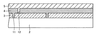
図1に示すように、本実施の形態における太陽電池パネル検査装置50の構成の一例について説明する。この太陽電池パネル検査装置50の検査対象である太陽電池パネル100は、図2に示すように、主表面2uを有する透明絶縁基板2と、透明絶縁基板2の主表面2uに順次積層された透明電極層3、半導体光電変換層4および裏面電極層5とを含み、透明絶縁基板2の外周近傍に透明絶縁基板2の主表面2uが露出する外周絶縁領域21を有している。太陽電池パネル検査装置50は、このような太陽電池パネル100に対して、外周絶縁領域21の絶縁性能を検査するための検査装置である。
(太陽電池パネル検査装置50Aおよび上流側装置52の構成)
図5に示すように、本実施の形態に使用する太陽電池パネル検査装置50A、および太陽電池パネル100の搬送方向からみて上流側に設置される上流側装置52の構成の一例について説明する。この太陽電池パネル検査装置50Aは、図2に示した、主表面2uを有する透明絶縁基板2と、透明絶縁基板2の主表面2uに順次積層された透明電極層3、半導体光電変換層4、および裏面電極層5とを含み、透明絶縁基板2の外周近傍に透明絶縁基板2の主表面2uが露出する外周絶縁領域21を有する太陽電池パネル100に対して、外周絶縁領域21の絶縁性能を検査するための検査装置である。
以下、図9から図17を参照して、本発明の光電変換装置の製造方法の一例として、実施の形態1における太陽電池パネル検査装置50を用いた太陽電池パネルの検査方法を製造工程に含む太陽電池パネルの製造方法、およびその太陽電池パネルを用いた薄膜太陽電池の製造方法について説明する。なお、本発明の図面において、同一の参照符号は、同一部分または相当部分を表わすものとする。
実施の形態2における太陽電池パネル検査装置50Aを用いた太陽電池パネルの検査方法を製造工程に含む太陽電池パネルの製造方法、およびその太陽電池パネルを用いた薄膜太陽電池の製造方法について説明する。説明は実施例1と異なる点のみ説明する。太陽電池パネル検査装置50Aの太陽電池パネル100の搬送方向からみて上流側にコンベヤーを有する上流側装置52を設け、この上流側装置52の筐体53の内部にも、水分量を管理する手段36Aおよび水分量を減少させる手段37Aを設けた。
Claims (9)
- 透明絶縁基板の主表面に順次積層された透明電極層、光電変換層、および裏面電極層を含み、前記透明絶縁基板の外周近傍に前記透明絶縁基板の前記主表面が露出する外周絶縁領域を有する太陽電池パネルに対して、前記外周絶縁領域の絶縁性能を検査するための太陽電池パネル検査装置であって、
検査対象の太陽電池パネルを収容する筐体と、
前記裏面電極層に当接させるための第1端子と、
前記外周絶縁領域の外周端近傍に当接させるための第2端子と、を有し、
前記第1端子と前記第2端子との端子間にそれぞれ電圧を印加するための電圧印加部と、
前記電圧印加部によって電圧を印加した前記第1端子と前記第2端子との間に流れる電流を検出する電流検出部と、
前記筐体内の絶対水分量を14.3g/m3以下に減少させる手段と、
を備え、
前記絶縁性能の検査は、前記太陽電池パネルに6000Vの電圧を印加して電流値が50μA未満であれば合格と判断する、太陽電池パネル検査装置。 - 前記絶対水分量を減少させる手段として、乾燥エアーを使用する、請求項1に記載の太陽電池パネル検査装置。
- 前記絶対水分量を減少させる手段として、除湿機を使用する、請求項1に記載の太陽電池パネル検査装置。
- 前記絶対水分量を減少させる手段として、乾燥剤を使用する、請求項1に記載の太陽電池パネル検査装置。
- 前記筐体内の絶対水分量を管理する手段をさらに備える、請求項1から4のいずれかに記載の太陽電池パネル検査装置。
- 前記絶対水分量を管理する手段として、前記筐体内の温度と湿度とを管理する、請求項5に記載の太陽電池パネル検査装置。
- 前記絶対水分量を管理する手段として、前記筐体内の最高温度時の湿度を管理する、請求項5または6に記載の太陽電池パネル検査装置。
- 透明絶縁基板の主表面に順次積層された透明電極層、光電変換層、および裏面電極層を含み、前記透明絶縁基板の外周近傍に前記透明絶縁基板の前記主表面が露出する外周絶縁領域を有する太陽電池パネルに対して、前記外周絶縁領域の絶縁性能を検査するため、請求項1から請求項7のいずれか1項に記載の太陽電池パネル検査装置を用いた太陽電池パネル検査方法であって、
検査対象の太陽電池パネル周囲の雰囲気の絶対水分量を14.3g/m3以下に減少させる工程と、
該絶対水分量を減少させる工程の後に、前記裏面電極層と前記外周絶縁領域の外周端近傍との間に流れる電流を検出する工程と、を含む太陽電池パネルの検査方法。 - 透明絶縁基板に設けられた透明電極層に、光電変換層および裏面電極層を積層する工程と、
前記透明絶縁基板の外周近傍に積層された前記透明電極層、前記光電変換層および前記裏面電極層を除去して、外周絶縁領域を形成する工程と、
前記透明絶縁基板周囲の雰囲気の絶対水分量を14.3g/m3以下に減少させる工程と、
該絶対水分量を減少させる工程の後に、前記裏面電極層と前記外周絶縁領域の外周端近傍との間に流れる電流を検出して、前記外周絶縁領域の絶縁性能を検査する工程と、を含み、
前記外周絶縁領域の絶縁性能を検査する工程は、請求項8に記載の太陽電池パネル検査方法を用いた太陽電池パネル検査方法である、
太陽電池パネルの製造方法。
Priority Applications (4)
| Application Number | Priority Date | Filing Date | Title |
|---|---|---|---|
| JP2010082942A JP5367630B2 (ja) | 2010-03-31 | 2010-03-31 | 太陽電池パネル検査装置、太陽電池パネルの検査方法、および太陽電池パネルの製造方法 |
| US13/638,092 US20130019942A1 (en) | 2010-03-31 | 2011-03-29 | Solar cell panel inspection device, method for inspecting solar cell panel, method for manufacturing solar cell panel, and solar cell panel |
| EP11765551A EP2555249A1 (en) | 2010-03-31 | 2011-03-29 | Solar panel inspection device, solar panel inspection method, solar panel manufacturing method, and solar panel |
| PCT/JP2011/057814 WO2011125651A1 (ja) | 2010-03-31 | 2011-03-29 | 太陽電池パネル検査装置、太陽電池パネルの検査方法、太陽電池パネルの製造方法、および太陽電池パネル |
Applications Claiming Priority (1)
| Application Number | Priority Date | Filing Date | Title |
|---|---|---|---|
| JP2010082942A JP5367630B2 (ja) | 2010-03-31 | 2010-03-31 | 太陽電池パネル検査装置、太陽電池パネルの検査方法、および太陽電池パネルの製造方法 |
Publications (2)
| Publication Number | Publication Date |
|---|---|
| JP2011216645A JP2011216645A (ja) | 2011-10-27 |
| JP5367630B2 true JP5367630B2 (ja) | 2013-12-11 |
Family
ID=44762598
Family Applications (1)
| Application Number | Title | Priority Date | Filing Date |
|---|---|---|---|
| JP2010082942A Expired - Fee Related JP5367630B2 (ja) | 2010-03-31 | 2010-03-31 | 太陽電池パネル検査装置、太陽電池パネルの検査方法、および太陽電池パネルの製造方法 |
Country Status (4)
| Country | Link |
|---|---|
| US (1) | US20130019942A1 (ja) |
| EP (1) | EP2555249A1 (ja) |
| JP (1) | JP5367630B2 (ja) |
| WO (1) | WO2011125651A1 (ja) |
Families Citing this family (11)
| Publication number | Priority date | Publication date | Assignee | Title |
|---|---|---|---|---|
| CN102788938A (zh) * | 2012-06-29 | 2012-11-21 | 苏州晟成新能源科技有限公司 | 显示屏可转动的绝缘测试机 |
| CN102788940A (zh) * | 2012-06-29 | 2012-11-21 | 苏州晟成新能源科技有限公司 | 输送宽度可调的绝缘测试机 |
| CN102721908A (zh) * | 2012-06-29 | 2012-10-10 | 苏州晟成新能源科技有限公司 | 具有识别功能的绝缘测试机 |
| CN103063682A (zh) * | 2012-12-25 | 2013-04-24 | 江苏赛拉弗光伏系统有限公司 | 太阳能电池组件用冷红外自动测试仪 |
| CN103018643B (zh) * | 2012-12-25 | 2015-02-25 | 江苏赛拉弗光伏系统有限公司 | 用于太阳能光伏组件的绝缘耐压自动测试装置 |
| EP2881994B1 (en) * | 2013-12-03 | 2018-02-14 | LG Electronics Inc. | Solar cell measuring apparatus |
| CN106026914B (zh) * | 2016-05-31 | 2017-12-26 | 宁夏银星能源光伏发电设备制造有限公司 | 一种通用型多栅线电池片测试装置 |
| JP6779668B2 (ja) * | 2016-05-31 | 2020-11-04 | ソーラーフロンティア株式会社 | 絶縁検査装置 |
| DE112018006853T5 (de) * | 2018-01-15 | 2020-10-08 | China Triumph International Engineering Co., Ltd. | Messanordnung zur sequentiellen Charakterisierung von Solarzellen eines Solarmoduls und Verfahren zur sequentiellen Charakterisierung von Solarzellen eines Solarmoduls mit dieser Messanordnung |
| JP7273786B2 (ja) * | 2020-12-28 | 2023-05-15 | プライムプラネットエナジー&ソリューションズ株式会社 | フィルム型電池の検査装置および製造方法 |
| IT202200024621A1 (it) * | 2022-11-29 | 2024-05-29 | Ecoprogetti S R L | Apparato simulatore solare |
Family Cites Families (3)
| Publication number | Priority date | Publication date | Assignee | Title |
|---|---|---|---|---|
| JP3519299B2 (ja) * | 1999-01-06 | 2004-04-12 | 芝府エンジニアリング株式会社 | 半導体装置 |
| JP4485506B2 (ja) | 2006-10-27 | 2010-06-23 | シャープ株式会社 | 薄膜太陽電池および薄膜太陽電池の製造方法 |
| JP2009206279A (ja) * | 2008-02-27 | 2009-09-10 | Sharp Corp | 薄膜太陽電池およびその製造方法 |
-
2010
- 2010-03-31 JP JP2010082942A patent/JP5367630B2/ja not_active Expired - Fee Related
-
2011
- 2011-03-29 EP EP11765551A patent/EP2555249A1/en not_active Withdrawn
- 2011-03-29 WO PCT/JP2011/057814 patent/WO2011125651A1/ja active Application Filing
- 2011-03-29 US US13/638,092 patent/US20130019942A1/en not_active Abandoned
Also Published As
| Publication number | Publication date |
|---|---|
| WO2011125651A1 (ja) | 2011-10-13 |
| EP2555249A1 (en) | 2013-02-06 |
| JP2011216645A (ja) | 2011-10-27 |
| US20130019942A1 (en) | 2013-01-24 |
Similar Documents
| Publication | Publication Date | Title |
|---|---|---|
| JP5367630B2 (ja) | 太陽電池パネル検査装置、太陽電池パネルの検査方法、および太陽電池パネルの製造方法 | |
| US6175075B1 (en) | Solar cell module excelling in reliability | |
| TWI413266B (zh) | 太陽能電池模組 | |
| US7906365B2 (en) | Method of manufacturing solar cell panel | |
| WO2009107517A1 (ja) | 薄膜太陽電池およびその製造方法 | |
| WO2010129136A2 (en) | Production line for the production of multiple sized photovoltaic devices | |
| EP2393120A1 (en) | Solar cell and method for manufacturing solar cell | |
| Xiong et al. | PV module durability testing under high voltage biased damp heat conditions | |
| WO2008026581A1 (fr) | Module de pile solaire | |
| CN102437215A (zh) | 用于薄膜光伏器件的叠层内圆片层及薄膜光伏器件的制造方法 | |
| JP2013120842A (ja) | 光電変換装置の検査方法及び検査装置 | |
| JP2007141967A (ja) | 光起電力素子、光起電力モジュールおよび光起電力素子の製造方法 | |
| JP2013098353A (ja) | 薄膜太陽電池モジュールの製造方法および検査方法 | |
| JP2010092893A (ja) | 薄膜太陽電池モジュールの製造方法 | |
| US20110008947A1 (en) | Apparatus and method for performing multifunction laser processes | |
| TW201347202A (zh) | 包含超薄彈性玻璃之多接面光伏打模組 | |
| Contreras et al. | Development of Cu (In, Ga) Se 2 test coupons for potential induced degradation studies | |
| JP2008053303A (ja) | 太陽電池パネル | |
| JP2012089789A (ja) | 太陽電池アレイの検査装置及びこれを用いた検査方法 | |
| CN116435396A (zh) | 光伏背板、光伏背板的制作方法及光伏组件 | |
| JP2011181826A (ja) | 光電変換装置の製造方法 | |
| WO2014050193A1 (ja) | 光電変換モジュール | |
| JP2009071192A (ja) | 光電変換装置、及びその製造方法 | |
| US12266732B2 (en) | Solar cell module and manufacturing method thereof | |
| US20230275169A1 (en) | Solar cell module and manufacturing method thereof |
Legal Events
| Date | Code | Title | Description |
|---|---|---|---|
| A521 | Request for written amendment filed |
Free format text: JAPANESE INTERMEDIATE CODE: A523 Effective date: 20110816 |
|
| A02 | Decision of refusal |
Free format text: JAPANESE INTERMEDIATE CODE: A02 Effective date: 20121002 |
|
| A521 | Request for written amendment filed |
Free format text: JAPANESE INTERMEDIATE CODE: A523 Effective date: 20121130 |
|
| A911 | Transfer to examiner for re-examination before appeal (zenchi) |
Free format text: JAPANESE INTERMEDIATE CODE: A911 Effective date: 20121207 |
|
| A912 | Re-examination (zenchi) completed and case transferred to appeal board |
Free format text: JAPANESE INTERMEDIATE CODE: A912 Effective date: 20130329 |
|
| A61 | First payment of annual fees (during grant procedure) |
Free format text: JAPANESE INTERMEDIATE CODE: A61 Effective date: 20130911 |
|
| R150 | Certificate of patent or registration of utility model |
Free format text: JAPANESE INTERMEDIATE CODE: R150 |
|
| LAPS | Cancellation because of no payment of annual fees |