JP5339270B2 - 液晶表示装置および電子機器 - Google Patents
液晶表示装置および電子機器 Download PDFInfo
- Publication number
- JP5339270B2 JP5339270B2 JP2008049789A JP2008049789A JP5339270B2 JP 5339270 B2 JP5339270 B2 JP 5339270B2 JP 2008049789 A JP2008049789 A JP 2008049789A JP 2008049789 A JP2008049789 A JP 2008049789A JP 5339270 B2 JP5339270 B2 JP 5339270B2
- Authority
- JP
- Japan
- Prior art keywords
- liquid crystal
- light shielding
- shielding member
- pixel
- spacer
- Prior art date
- Legal status (The legal status is an assumption and is not a legal conclusion. Google has not performed a legal analysis and makes no representation as to the accuracy of the status listed.)
- Expired - Fee Related
Links
Images


Classifications
-
- G—PHYSICS
- G02—OPTICS
- G02F—OPTICAL DEVICES OR ARRANGEMENTS FOR THE CONTROL OF LIGHT BY MODIFICATION OF THE OPTICAL PROPERTIES OF THE MEDIA OF THE ELEMENTS INVOLVED THEREIN; NON-LINEAR OPTICS; FREQUENCY-CHANGING OF LIGHT; OPTICAL LOGIC ELEMENTS; OPTICAL ANALOGUE/DIGITAL CONVERTERS
- G02F1/00—Devices or arrangements for the control of the intensity, colour, phase, polarisation or direction of light arriving from an independent light source, e.g. switching, gating or modulating; Non-linear optics
- G02F1/01—Devices or arrangements for the control of the intensity, colour, phase, polarisation or direction of light arriving from an independent light source, e.g. switching, gating or modulating; Non-linear optics for the control of the intensity, phase, polarisation or colour
- G02F1/13—Devices or arrangements for the control of the intensity, colour, phase, polarisation or direction of light arriving from an independent light source, e.g. switching, gating or modulating; Non-linear optics for the control of the intensity, phase, polarisation or colour based on liquid crystals, e.g. single liquid crystal display cells
- G02F1/133—Constructional arrangements; Operation of liquid crystal cells; Circuit arrangements
- G02F1/1333—Constructional arrangements; Manufacturing methods
- G02F1/1335—Structural association of cells with optical devices, e.g. polarisers or reflectors
- G02F1/133509—Filters, e.g. light shielding masks
- G02F1/133512—Light shielding layers, e.g. black matrix
-
- G—PHYSICS
- G02—OPTICS
- G02F—OPTICAL DEVICES OR ARRANGEMENTS FOR THE CONTROL OF LIGHT BY MODIFICATION OF THE OPTICAL PROPERTIES OF THE MEDIA OF THE ELEMENTS INVOLVED THEREIN; NON-LINEAR OPTICS; FREQUENCY-CHANGING OF LIGHT; OPTICAL LOGIC ELEMENTS; OPTICAL ANALOGUE/DIGITAL CONVERTERS
- G02F1/00—Devices or arrangements for the control of the intensity, colour, phase, polarisation or direction of light arriving from an independent light source, e.g. switching, gating or modulating; Non-linear optics
- G02F1/01—Devices or arrangements for the control of the intensity, colour, phase, polarisation or direction of light arriving from an independent light source, e.g. switching, gating or modulating; Non-linear optics for the control of the intensity, phase, polarisation or colour
- G02F1/13—Devices or arrangements for the control of the intensity, colour, phase, polarisation or direction of light arriving from an independent light source, e.g. switching, gating or modulating; Non-linear optics for the control of the intensity, phase, polarisation or colour based on liquid crystals, e.g. single liquid crystal display cells
- G02F1/133—Constructional arrangements; Operation of liquid crystal cells; Circuit arrangements
- G02F1/1333—Constructional arrangements; Manufacturing methods
- G02F1/1335—Structural association of cells with optical devices, e.g. polarisers or reflectors
-
- G—PHYSICS
- G02—OPTICS
- G02F—OPTICAL DEVICES OR ARRANGEMENTS FOR THE CONTROL OF LIGHT BY MODIFICATION OF THE OPTICAL PROPERTIES OF THE MEDIA OF THE ELEMENTS INVOLVED THEREIN; NON-LINEAR OPTICS; FREQUENCY-CHANGING OF LIGHT; OPTICAL LOGIC ELEMENTS; OPTICAL ANALOGUE/DIGITAL CONVERTERS
- G02F1/00—Devices or arrangements for the control of the intensity, colour, phase, polarisation or direction of light arriving from an independent light source, e.g. switching, gating or modulating; Non-linear optics
- G02F1/01—Devices or arrangements for the control of the intensity, colour, phase, polarisation or direction of light arriving from an independent light source, e.g. switching, gating or modulating; Non-linear optics for the control of the intensity, phase, polarisation or colour
- G02F1/13—Devices or arrangements for the control of the intensity, colour, phase, polarisation or direction of light arriving from an independent light source, e.g. switching, gating or modulating; Non-linear optics for the control of the intensity, phase, polarisation or colour based on liquid crystals, e.g. single liquid crystal display cells
- G02F1/133—Constructional arrangements; Operation of liquid crystal cells; Circuit arrangements
- G02F1/1333—Constructional arrangements; Manufacturing methods
- G02F1/1339—Gaskets; Spacers; Sealing of cells
-
- G—PHYSICS
- G02—OPTICS
- G02F—OPTICAL DEVICES OR ARRANGEMENTS FOR THE CONTROL OF LIGHT BY MODIFICATION OF THE OPTICAL PROPERTIES OF THE MEDIA OF THE ELEMENTS INVOLVED THEREIN; NON-LINEAR OPTICS; FREQUENCY-CHANGING OF LIGHT; OPTICAL LOGIC ELEMENTS; OPTICAL ANALOGUE/DIGITAL CONVERTERS
- G02F1/00—Devices or arrangements for the control of the intensity, colour, phase, polarisation or direction of light arriving from an independent light source, e.g. switching, gating or modulating; Non-linear optics
- G02F1/01—Devices or arrangements for the control of the intensity, colour, phase, polarisation or direction of light arriving from an independent light source, e.g. switching, gating or modulating; Non-linear optics for the control of the intensity, phase, polarisation or colour
- G02F1/13—Devices or arrangements for the control of the intensity, colour, phase, polarisation or direction of light arriving from an independent light source, e.g. switching, gating or modulating; Non-linear optics for the control of the intensity, phase, polarisation or colour based on liquid crystals, e.g. single liquid crystal display cells
- G02F1/133—Constructional arrangements; Operation of liquid crystal cells; Circuit arrangements
- G02F1/13306—Circuit arrangements or driving methods for the control of single liquid crystal cells
- G02F1/13312—Circuits comprising photodetectors for purposes other than feedback
-
- G—PHYSICS
- G02—OPTICS
- G02F—OPTICAL DEVICES OR ARRANGEMENTS FOR THE CONTROL OF LIGHT BY MODIFICATION OF THE OPTICAL PROPERTIES OF THE MEDIA OF THE ELEMENTS INVOLVED THEREIN; NON-LINEAR OPTICS; FREQUENCY-CHANGING OF LIGHT; OPTICAL LOGIC ELEMENTS; OPTICAL ANALOGUE/DIGITAL CONVERTERS
- G02F1/00—Devices or arrangements for the control of the intensity, colour, phase, polarisation or direction of light arriving from an independent light source, e.g. switching, gating or modulating; Non-linear optics
- G02F1/01—Devices or arrangements for the control of the intensity, colour, phase, polarisation or direction of light arriving from an independent light source, e.g. switching, gating or modulating; Non-linear optics for the control of the intensity, phase, polarisation or colour
- G02F1/13—Devices or arrangements for the control of the intensity, colour, phase, polarisation or direction of light arriving from an independent light source, e.g. switching, gating or modulating; Non-linear optics for the control of the intensity, phase, polarisation or colour based on liquid crystals, e.g. single liquid crystal display cells
- G02F1/133—Constructional arrangements; Operation of liquid crystal cells; Circuit arrangements
- G02F1/1333—Constructional arrangements; Manufacturing methods
- G02F1/1337—Surface-induced orientation of the liquid crystal molecules, e.g. by alignment layers
- G02F1/133707—Structures for producing distorted electric fields, e.g. bumps, protrusions, recesses, slits in pixel electrodes
-
- G—PHYSICS
- G02—OPTICS
- G02F—OPTICAL DEVICES OR ARRANGEMENTS FOR THE CONTROL OF LIGHT BY MODIFICATION OF THE OPTICAL PROPERTIES OF THE MEDIA OF THE ELEMENTS INVOLVED THEREIN; NON-LINEAR OPTICS; FREQUENCY-CHANGING OF LIGHT; OPTICAL LOGIC ELEMENTS; OPTICAL ANALOGUE/DIGITAL CONVERTERS
- G02F1/00—Devices or arrangements for the control of the intensity, colour, phase, polarisation or direction of light arriving from an independent light source, e.g. switching, gating or modulating; Non-linear optics
- G02F1/01—Devices or arrangements for the control of the intensity, colour, phase, polarisation or direction of light arriving from an independent light source, e.g. switching, gating or modulating; Non-linear optics for the control of the intensity, phase, polarisation or colour
- G02F1/13—Devices or arrangements for the control of the intensity, colour, phase, polarisation or direction of light arriving from an independent light source, e.g. switching, gating or modulating; Non-linear optics for the control of the intensity, phase, polarisation or colour based on liquid crystals, e.g. single liquid crystal display cells
- G02F1/133—Constructional arrangements; Operation of liquid crystal cells; Circuit arrangements
- G02F1/1333—Constructional arrangements; Manufacturing methods
- G02F1/1339—Gaskets; Spacers; Sealing of cells
- G02F1/13394—Gaskets; Spacers; Sealing of cells spacers regularly patterned on the cell subtrate, e.g. walls, pillars
-
- G—PHYSICS
- G09—EDUCATION; CRYPTOGRAPHY; DISPLAY; ADVERTISING; SEALS
- G09G—ARRANGEMENTS OR CIRCUITS FOR CONTROL OF INDICATING DEVICES USING STATIC MEANS TO PRESENT VARIABLE INFORMATION
- G09G2360/00—Aspects of the architecture of display systems
- G09G2360/14—Detecting light within display terminals, e.g. using a single or a plurality of photosensors
- G09G2360/145—Detecting light within display terminals, e.g. using a single or a plurality of photosensors the light originating from the display screen
- G09G2360/147—Detecting light within display terminals, e.g. using a single or a plurality of photosensors the light originating from the display screen the originated light output being determined for each pixel
- G09G2360/148—Detecting light within display terminals, e.g. using a single or a plurality of photosensors the light originating from the display screen the originated light output being determined for each pixel the light being detected by light detection means within each pixel
Landscapes
- Physics & Mathematics (AREA)
- Nonlinear Science (AREA)
- Mathematical Physics (AREA)
- Chemical & Material Sciences (AREA)
- Crystallography & Structural Chemistry (AREA)
- General Physics & Mathematics (AREA)
- Optics & Photonics (AREA)
- Liquid Crystal (AREA)
Description
図1は、実施形態の液晶表示装置の構成を説明する平面構成図である。図2は、実施形態の液晶表示装置の構成を説明する断面構成図であり、図1におけるA−A’断面図である。以下にこれらの図面に基づいて実施形態の液晶表示装置の概略構成を説明する。
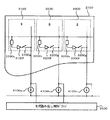
図3は、上記液晶表示装置の駆動回路の一例を示す図である。
図4は、画素の構成例について説明する模式図である。液晶表示装置の表示領域には、複数の画素(主画素P)がマトリクス状に配置されている。主画素Pは複数の副画素によって構成され、図4に示す例ではR(赤)に対応した副画素p1、G(緑)に対応した副画素p2、B(青)に対応した副画素p3の3つの副画素によって1つの主画素Pが構成されている。なお、主画素Pを構成する副画素の種類や配列は上記以外であってもよいが、本実施形態ではRGB3つの副画素p1〜p3によって1つの主画素Pが構成されるものを例とする。
図8は、具体的な実施形態(その1)を説明する模式断面図で、本実施形態に係る液晶表示装置の一つの副画素の構造を示したものとなっている。本実施形態の液晶表示装置は、垂直配向(VA:Vertical Alignment)モードの液晶LCを適用しており、配向制御には液晶配向制御因子40として、対向基板20側にポジレジストで突起を形成した構造を採用している。

図9は、具体的な実施形態(その2)を説明する模式断面図、図10は、具体的な実施形態(その2)を説明する模式平面図で、本実施形態に係る液晶表示装置の一つの副画素の構造を示したものとなっている。
遮光部材Sを駆動基板10側に設ける構成では、CS(補助容量)を形成する金属膜を遮光部材Sとして流用し、容量に寄与しない領域を延長して遮光部材Sと同様の効果を得ることができる。
製品の仕様に対応した白色色度座標にカラーフィルタの色度を変更することなく合わせることができることから、特性の低下を抑制しつつ所望の仕様に対応することが可能となる。また、予め配置される遮光手段を遮光部材Sとして兼用することから、駆動基板10や対向基板20にパターンを形成する際に用いるフォトリソグラフィ用マスクの簡単な設計変更のみで対応することが可能なため、製造時間の増加やコストアップを抑制することが可能となる。
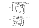
本実施形態に係る表示装置は、図14に示すようにフラット型のモジュール形状のものを含む。例えば絶縁性の基板上2002に、液晶素子、薄膜トランジスタ、薄膜容量、受光素子等からなる画素をマトリックス状に集積形成した画素アレイ部2002aを設ける、この画素アレイ部(画素マトリックス部)2002aを囲むように接着剤2021を配し、ガラス等の対向基板2006を貼り付けて表示モジュールとする。この透明な対向基板2006には必要に応じて、カラーフィルタ、保護膜、遮光膜等を設けてもよい。表示モジュールには、外部から画素アレイ部2002aへの信号等を入出力するためのコネクタとして例えばFPC(フレキシブルプリントサーキット)2023を設けてもよい。
本実施形態に係る表示装置は、以下のような表示撮像装置に適用可能である。また、この表示撮像装置は、先に説明した各種電子機器に適用可能である。図20には、表示撮像装置の全体構成を表すものである。この表示撮像装置は、I/Oディスプレイパネル2000と、バックライト1500と、表示ドライブ回路1200と、受光ドライブ回路1300と、画像処理部1400と、アプリケーションプログラム実行部1100とを備えている。
Claims (4)
- 駆動基板と対向基板との間に液晶を有し、表示領域として複数の主画素が配置された液晶表示装置において、
前記主画素を構成する複数の副画素のうち少なくとも2つの副画素に基板間隔設定用のスペーサが設けられ、
前記少なくとも2つの副画素において前記スペーサに対応して設けられる遮光部材の平面視面積が異なっていて、
前記遮光部材の形状は、前記スペーサの平面視外形と相似形であり、
前記スペーサは、前記対向基板上に予め形成された柱状スペーサであり、
前記遮光部材は、前記駆動基板側の前記スペーサと対向する位置に設けられている、
ことを特徴とする液晶表示装置。 - 前記遮光部材は、前記駆動基板側に設けられた透明電極内に設けられている、
ことを特徴とする請求項1記載の液晶表示装置。 - 前記遮光部材は、前記表示領域内に独立して配置されている
ことを特徴とする請求項2記載の液晶表示装置。 - 本体筐体に液晶表示装置が設けられた電子機器において、
前記液晶表示装置は、
駆動基板と対向基板との間に液晶が封入され、表示領域として複数の主画素が配置されており、
前記主画素を構成する複数の副画素のうち少なくとも2つの副画素に基板間隔設定用のスペーサが設けられ、
前記少なくとも2つの副画素において前記スペーサに対応して設けられる遮光部材の平面視面積が異なっていて、
前記遮光部材の形状は、前記スペーサの平面視外形と相似形であり、
前記スペーサは、前記対向基板上に予め形成された柱状スペーサであり、
前記遮光部材は、前記駆動基板側の前記スペーサと対向する位置に設けられている、
ことを特徴とする電子機器。
Priority Applications (5)
| Application Number | Priority Date | Filing Date | Title |
|---|---|---|---|
| JP2008049789A JP5339270B2 (ja) | 2008-02-29 | 2008-02-29 | 液晶表示装置および電子機器 |
| TW098104383A TWI459075B (zh) | 2008-02-29 | 2009-02-11 | 液晶顯示元件及電子裝置 |
| KR1020090012824A KR20090093812A (ko) | 2008-02-29 | 2009-02-17 | 액정 표시 장치 및 전자 기기 |
| US12/389,787 US20090219458A1 (en) | 2008-02-29 | 2009-02-20 | Liquid crystal display device and electronic apparatus |
| CN2009101183386A CN101520566B (zh) | 2008-02-29 | 2009-02-27 | 液晶显示装置和电子设备 |
Applications Claiming Priority (1)
| Application Number | Priority Date | Filing Date | Title |
|---|---|---|---|
| JP2008049789A JP5339270B2 (ja) | 2008-02-29 | 2008-02-29 | 液晶表示装置および電子機器 |
Publications (2)
| Publication Number | Publication Date |
|---|---|
| JP2009205088A JP2009205088A (ja) | 2009-09-10 |
| JP5339270B2 true JP5339270B2 (ja) | 2013-11-13 |
Family
ID=41012914
Family Applications (1)
| Application Number | Title | Priority Date | Filing Date |
|---|---|---|---|
| JP2008049789A Expired - Fee Related JP5339270B2 (ja) | 2008-02-29 | 2008-02-29 | 液晶表示装置および電子機器 |
Country Status (5)
| Country | Link |
|---|---|
| US (1) | US20090219458A1 (ja) |
| JP (1) | JP5339270B2 (ja) |
| KR (1) | KR20090093812A (ja) |
| CN (1) | CN101520566B (ja) |
| TW (1) | TWI459075B (ja) |
Families Citing this family (8)
| Publication number | Priority date | Publication date | Assignee | Title |
|---|---|---|---|---|
| JP5311299B2 (ja) * | 2008-06-03 | 2013-10-09 | 株式会社ジャパンディスプレイ | 液晶表示装置 |
| US9291859B2 (en) | 2012-06-20 | 2016-03-22 | Samsung Display Co., Ltd. | Liquid crystal display |
| KR101994972B1 (ko) * | 2012-06-20 | 2019-07-02 | 삼성디스플레이 주식회사 | 액정 표시 장치 |
| JP6220628B2 (ja) | 2013-10-18 | 2017-10-25 | 株式会社ジャパンディスプレイ | 表示装置 |
| JP2015141749A (ja) * | 2014-01-27 | 2015-08-03 | 株式会社ジャパンディスプレイ | 表示装置およびその製造方法 |
| JP2015146304A (ja) | 2014-02-04 | 2015-08-13 | ソニー株式会社 | 表示装置、および電子機器 |
| TWI540372B (zh) * | 2015-06-25 | 2016-07-01 | 友達光電股份有限公司 | 畫素結構 |
| CN109613774A (zh) * | 2019-01-10 | 2019-04-12 | 深圳市华星光电半导体显示技术有限公司 | 像素结构及液晶显示面板 |
Family Cites Families (12)
| Publication number | Priority date | Publication date | Assignee | Title |
|---|---|---|---|---|
| JPH0884347A (ja) * | 1994-09-09 | 1996-03-26 | Sony Corp | カラー液晶表示装置 |
| JP3472422B2 (ja) * | 1996-11-07 | 2003-12-02 | シャープ株式会社 | 液晶装置の製造方法 |
| US6927824B1 (en) * | 1999-09-16 | 2005-08-09 | Fujitsu Display Technologies Corporation | Liquid crystal display device and thin film transistor substrate |
| JP4132528B2 (ja) * | 2000-01-14 | 2008-08-13 | シャープ株式会社 | 液晶表示装置の製造方法 |
| JP2002014353A (ja) * | 2000-06-30 | 2002-01-18 | Sony Corp | 液晶表示装置及びその製造方法 |
| JP3941481B2 (ja) * | 2000-12-22 | 2007-07-04 | セイコーエプソン株式会社 | 液晶表示装置および電子機器 |
| JP4056326B2 (ja) * | 2002-08-30 | 2008-03-05 | シャープ株式会社 | 液晶表示装置 |
| US7480022B2 (en) * | 2003-12-10 | 2009-01-20 | Seiko Epson Corporation | Liquid crystal display device, method of manufacturing liquid crystal display device, and electronic apparatus |
| JP4717533B2 (ja) * | 2005-07-06 | 2011-07-06 | 株式会社 日立ディスプレイズ | 表示装置 |
| JP2008033117A (ja) * | 2006-07-31 | 2008-02-14 | Epson Imaging Devices Corp | 液晶パネル |
| JP2008216423A (ja) * | 2007-03-01 | 2008-09-18 | Epson Imaging Devices Corp | 液晶装置及び電子機器 |
| TWI358595B (en) * | 2007-03-09 | 2012-02-21 | Au Optronics Corp | Liquid crystal display panel |
-
2008
- 2008-02-29 JP JP2008049789A patent/JP5339270B2/ja not_active Expired - Fee Related
-
2009
- 2009-02-11 TW TW098104383A patent/TWI459075B/zh not_active IP Right Cessation
- 2009-02-17 KR KR1020090012824A patent/KR20090093812A/ko not_active Application Discontinuation
- 2009-02-20 US US12/389,787 patent/US20090219458A1/en not_active Abandoned
- 2009-02-27 CN CN2009101183386A patent/CN101520566B/zh not_active Expired - Fee Related
Also Published As
| Publication number | Publication date |
|---|---|
| CN101520566B (zh) | 2011-06-15 |
| TWI459075B (zh) | 2014-11-01 |
| US20090219458A1 (en) | 2009-09-03 |
| JP2009205088A (ja) | 2009-09-10 |
| CN101520566A (zh) | 2009-09-02 |
| TW200949361A (en) | 2009-12-01 |
| KR20090093812A (ko) | 2009-09-02 |
Similar Documents
| Publication | Publication Date | Title |
|---|---|---|
| CN111708230B (zh) | 一种显示面板及显示装置 | |
| JP5339270B2 (ja) | 液晶表示装置および電子機器 | |
| JP5024110B2 (ja) | 電気光学装置及び電子機器 | |
| TWI381231B (zh) | 液晶顯示裝置 | |
| CN102540528B (zh) | 显示面板及其驱动方法 | |
| US10261617B2 (en) | In-cell touch panel and display device | |
| US8558974B2 (en) | Liquid crystal display apparatus | |
| US20100194704A1 (en) | Display device, touch sensor, and method for manufacturing display device | |
| CN102566135A (zh) | 显示装置 | |
| TWI481925B (zh) | 顯示裝置,其製造方法,及電子裝置 | |
| US9549173B2 (en) | Display device | |
| JP6498765B2 (ja) | タッチパネル、及び表示装置 | |
| JP4952166B2 (ja) | 液晶装置 | |
| US9093043B2 (en) | Display device and electronic apparatus | |
| JP5909202B2 (ja) | 表示装置及び電子機器 | |
| CN102096253B (zh) | 电光装置和电子设备 | |
| JP2010210734A (ja) | 液晶装置及び電子機器 | |
| JP2011082098A (ja) | 有機el装置、電気光学装置及び電子機器 | |
| JP5861740B2 (ja) | 電気光学装置及び電子機器 | |
| JP2008281732A (ja) | 電気光学装置及び電子機器 | |
| JP5678992B2 (ja) | 電気光学装置及び電子機器 | |
| JP2012128070A (ja) | 電子機器 |
Legal Events
| Date | Code | Title | Description |
|---|---|---|---|
| A521 | Written amendment |
Free format text: JAPANESE INTERMEDIATE CODE: A821 Effective date: 20091014 |
|
| RD02 | Notification of acceptance of power of attorney |
Free format text: JAPANESE INTERMEDIATE CODE: A7422 Effective date: 20091014 |
|
| RD04 | Notification of resignation of power of attorney |
Free format text: JAPANESE INTERMEDIATE CODE: A7424 Effective date: 20091030 |
|
| A621 | Written request for application examination |
Free format text: JAPANESE INTERMEDIATE CODE: A621 Effective date: 20110105 |
|
| A711 | Notification of change in applicant |
Free format text: JAPANESE INTERMEDIATE CODE: A711 Effective date: 20120330 |
|
| A131 | Notification of reasons for refusal |
Free format text: JAPANESE INTERMEDIATE CODE: A131 Effective date: 20120619 |
|
| A977 | Report on retrieval |
Free format text: JAPANESE INTERMEDIATE CODE: A971007 Effective date: 20120620 |
|
| A521 | Written amendment |
Free format text: JAPANESE INTERMEDIATE CODE: A523 Effective date: 20120809 |
|
| RD03 | Notification of appointment of power of attorney |
Free format text: JAPANESE INTERMEDIATE CODE: A7423 Effective date: 20130328 |
|
| A131 | Notification of reasons for refusal |
Free format text: JAPANESE INTERMEDIATE CODE: A131 Effective date: 20130416 |
|
| A521 | Written amendment |
Free format text: JAPANESE INTERMEDIATE CODE: A523 Effective date: 20130617 |
|
| TRDD | Decision of grant or rejection written | ||
| A01 | Written decision to grant a patent or to grant a registration (utility model) |
Free format text: JAPANESE INTERMEDIATE CODE: A01 Effective date: 20130723 |
|
| A711 | Notification of change in applicant |
Free format text: JAPANESE INTERMEDIATE CODE: A712 Effective date: 20130730 |
|
| A61 | First payment of annual fees (during grant procedure) |
Free format text: JAPANESE INTERMEDIATE CODE: A61 Effective date: 20130730 |
|
| R150 | Certificate of patent or registration of utility model |
Ref document number: 5339270 Country of ref document: JP Free format text: JAPANESE INTERMEDIATE CODE: R150 Free format text: JAPANESE INTERMEDIATE CODE: R150 |
|
| R250 | Receipt of annual fees |
Free format text: JAPANESE INTERMEDIATE CODE: R250 |
|
| R250 | Receipt of annual fees |
Free format text: JAPANESE INTERMEDIATE CODE: R250 |
|
| R250 | Receipt of annual fees |
Free format text: JAPANESE INTERMEDIATE CODE: R250 |
|
| LAPS | Cancellation because of no payment of annual fees |