JP5074201B2 - Electronic component mounting board - Google Patents
Electronic component mounting board Download PDFInfo
- Publication number
- JP5074201B2 JP5074201B2 JP2007546454A JP2007546454A JP5074201B2 JP 5074201 B2 JP5074201 B2 JP 5074201B2 JP 2007546454 A JP2007546454 A JP 2007546454A JP 2007546454 A JP2007546454 A JP 2007546454A JP 5074201 B2 JP5074201 B2 JP 5074201B2
- Authority
- JP
- Japan
- Prior art keywords
- frame
- surface electrode
- metal
- electrode
- electronic component
- Prior art date
- Legal status (The legal status is an assumption and is not a legal conclusion. Google has not performed a legal analysis and makes no representation as to the accuracy of the status listed.)
- Expired - Fee Related
Links
- 229910052751 metal Inorganic materials 0.000 claims description 147
- 239000002184 metal Substances 0.000 claims description 147
- 239000010410 layer Substances 0.000 claims description 89
- 239000000758 substrate Substances 0.000 claims description 57
- 239000012790 adhesive layer Substances 0.000 claims description 40
- 239000004065 semiconductor Substances 0.000 claims description 24
- 230000002093 peripheral effect Effects 0.000 claims description 6
- 239000007769 metal material Substances 0.000 claims description 2
- 238000000034 method Methods 0.000 description 40
- 239000011347 resin Substances 0.000 description 34
- 229920005989 resin Polymers 0.000 description 34
- 239000004020 conductor Substances 0.000 description 21
- 238000007747 plating Methods 0.000 description 17
- 230000000694 effects Effects 0.000 description 13
- 229910000679 solder Inorganic materials 0.000 description 12
- 238000003466 welding Methods 0.000 description 12
- 239000000463 material Substances 0.000 description 11
- 229910052737 gold Inorganic materials 0.000 description 10
- 229910052709 silver Inorganic materials 0.000 description 10
- 230000004888 barrier function Effects 0.000 description 9
- 229910052802 copper Inorganic materials 0.000 description 9
- 238000009713 electroplating Methods 0.000 description 9
- 238000005530 etching Methods 0.000 description 9
- 238000004519 manufacturing process Methods 0.000 description 9
- 229910045601 alloy Inorganic materials 0.000 description 6
- 239000000956 alloy Substances 0.000 description 6
- 239000000919 ceramic Substances 0.000 description 6
- 229910052759 nickel Inorganic materials 0.000 description 6
- 229910001111 Fine metal Inorganic materials 0.000 description 5
- 229910052782 aluminium Inorganic materials 0.000 description 5
- 238000007772 electroless plating Methods 0.000 description 5
- 239000003822 epoxy resin Substances 0.000 description 5
- 229920000647 polyepoxide Polymers 0.000 description 5
- 239000002335 surface treatment layer Substances 0.000 description 5
- 238000009792 diffusion process Methods 0.000 description 4
- 230000017525 heat dissipation Effects 0.000 description 4
- 229910052763 palladium Inorganic materials 0.000 description 4
- 239000000243 solution Substances 0.000 description 4
- 229910052718 tin Inorganic materials 0.000 description 4
- XOLBLPGZBRYERU-UHFFFAOYSA-N tin dioxide Chemical compound O=[Sn]=O XOLBLPGZBRYERU-UHFFFAOYSA-N 0.000 description 4
- 238000010586 diagram Methods 0.000 description 3
- 230000020169 heat generation Effects 0.000 description 3
- 150000002739 metals Chemical class 0.000 description 3
- OKTJSMMVPCPJKN-UHFFFAOYSA-N Carbon Chemical compound [C] OKTJSMMVPCPJKN-UHFFFAOYSA-N 0.000 description 2
- MHAJPDPJQMAIIY-UHFFFAOYSA-N Hydrogen peroxide Chemical compound OO MHAJPDPJQMAIIY-UHFFFAOYSA-N 0.000 description 2
- QAOWNCQODCNURD-UHFFFAOYSA-N Sulfuric acid Chemical compound OS(O)(=O)=O QAOWNCQODCNURD-UHFFFAOYSA-N 0.000 description 2
- ROOXNKNUYICQNP-UHFFFAOYSA-N ammonium persulfate Chemical compound [NH4+].[NH4+].[O-]S(=O)(=O)OOS([O-])(=O)=O ROOXNKNUYICQNP-UHFFFAOYSA-N 0.000 description 2
- 230000015572 biosynthetic process Effects 0.000 description 2
- 229910052799 carbon Inorganic materials 0.000 description 2
- 230000001965 increasing effect Effects 0.000 description 2
- 229910052742 iron Inorganic materials 0.000 description 2
- 229910044991 metal oxide Inorganic materials 0.000 description 2
- 150000004706 metal oxides Chemical class 0.000 description 2
- 238000007789 sealing Methods 0.000 description 2
- 239000000126 substance Substances 0.000 description 2
- 239000004925 Acrylic resin Substances 0.000 description 1
- 229920000178 Acrylic resin Polymers 0.000 description 1
- 229910001020 Au alloy Inorganic materials 0.000 description 1
- 229910020218 Pb—Zn Inorganic materials 0.000 description 1
- OAICVXFJPJFONN-UHFFFAOYSA-N Phosphorus Chemical compound [P] OAICVXFJPJFONN-UHFFFAOYSA-N 0.000 description 1
- XUIMIQQOPSSXEZ-UHFFFAOYSA-N Silicon Chemical compound [Si] XUIMIQQOPSSXEZ-UHFFFAOYSA-N 0.000 description 1
- -1 SnO2) with a resin Chemical class 0.000 description 1
- 239000000853 adhesive Substances 0.000 description 1
- 230000001070 adhesive effect Effects 0.000 description 1
- 229910001870 ammonium persulfate Inorganic materials 0.000 description 1
- 230000000740 bleeding effect Effects 0.000 description 1
- 238000005219 brazing Methods 0.000 description 1
- 239000003575 carbonaceous material Substances 0.000 description 1
- 239000003054 catalyst Substances 0.000 description 1
- 229910010293 ceramic material Inorganic materials 0.000 description 1
- 238000011109 contamination Methods 0.000 description 1
- 238000002788 crimping Methods 0.000 description 1
- 238000010894 electron beam technology Methods 0.000 description 1
- 230000002708 enhancing effect Effects 0.000 description 1
- 230000001747 exhibiting effect Effects 0.000 description 1
- 239000011810 insulating material Substances 0.000 description 1
- 230000010354 integration Effects 0.000 description 1
- 230000001788 irregular Effects 0.000 description 1
- 238000010030 laminating Methods 0.000 description 1
- 229910052749 magnesium Inorganic materials 0.000 description 1
- 238000002844 melting Methods 0.000 description 1
- 230000008018 melting Effects 0.000 description 1
- 239000011259 mixed solution Substances 0.000 description 1
- 230000035515 penetration Effects 0.000 description 1
- 230000000630 rising effect Effects 0.000 description 1
- 229910052710 silicon Inorganic materials 0.000 description 1
- 239000010703 silicon Substances 0.000 description 1
- 238000005476 soldering Methods 0.000 description 1
- 238000004544 sputter deposition Methods 0.000 description 1
- 239000002344 surface layer Substances 0.000 description 1
- 238000007740 vapor deposition Methods 0.000 description 1
Images


Classifications
-
- H—ELECTRICITY
- H10—SEMICONDUCTOR DEVICES; ELECTRIC SOLID-STATE DEVICES NOT OTHERWISE PROVIDED FOR
- H10H—INORGANIC LIGHT-EMITTING SEMICONDUCTOR DEVICES HAVING POTENTIAL BARRIERS
- H10H20/00—Individual inorganic light-emitting semiconductor devices having potential barriers, e.g. light-emitting diodes [LED]
- H10H20/80—Constructional details
- H10H20/85—Packages
- H10H20/858—Means for heat extraction or cooling
- H10H20/8582—Means for heat extraction or cooling characterised by their shape
-
- H—ELECTRICITY
- H05—ELECTRIC TECHNIQUES NOT OTHERWISE PROVIDED FOR
- H05K—PRINTED CIRCUITS; CASINGS OR CONSTRUCTIONAL DETAILS OF ELECTRIC APPARATUS; MANUFACTURE OF ASSEMBLAGES OF ELECTRICAL COMPONENTS
- H05K1/00—Printed circuits
- H05K1/02—Details
- H05K1/0201—Thermal arrangements, e.g. for cooling, heating or preventing overheating
- H05K1/0203—Cooling of mounted components
-
- H—ELECTRICITY
- H10—SEMICONDUCTOR DEVICES; ELECTRIC SOLID-STATE DEVICES NOT OTHERWISE PROVIDED FOR
- H10H—INORGANIC LIGHT-EMITTING SEMICONDUCTOR DEVICES HAVING POTENTIAL BARRIERS
- H10H20/00—Individual inorganic light-emitting semiconductor devices having potential barriers, e.g. light-emitting diodes [LED]
- H10H20/80—Constructional details
- H10H20/85—Packages
- H10H20/855—Optical field-shaping means, e.g. lenses
- H10H20/856—Reflecting means
-
- H—ELECTRICITY
- H01—ELECTRIC ELEMENTS
- H01L—SEMICONDUCTOR DEVICES NOT COVERED BY CLASS H10
- H01L2224/00—Indexing scheme for arrangements for connecting or disconnecting semiconductor or solid-state bodies and methods related thereto as covered by H01L24/00
- H01L2224/01—Means for bonding being attached to, or being formed on, the surface to be connected, e.g. chip-to-package, die-attach, "first-level" interconnects; Manufacturing methods related thereto
- H01L2224/26—Layer connectors, e.g. plate connectors, solder or adhesive layers; Manufacturing methods related thereto
- H01L2224/31—Structure, shape, material or disposition of the layer connectors after the connecting process
- H01L2224/32—Structure, shape, material or disposition of the layer connectors after the connecting process of an individual layer connector
- H01L2224/321—Disposition
- H01L2224/32151—Disposition the layer connector connecting between a semiconductor or solid-state body and an item not being a semiconductor or solid-state body, e.g. chip-to-substrate, chip-to-passive
- H01L2224/32221—Disposition the layer connector connecting between a semiconductor or solid-state body and an item not being a semiconductor or solid-state body, e.g. chip-to-substrate, chip-to-passive the body and the item being stacked
- H01L2224/32225—Disposition the layer connector connecting between a semiconductor or solid-state body and an item not being a semiconductor or solid-state body, e.g. chip-to-substrate, chip-to-passive the body and the item being stacked the item being non-metallic, e.g. insulating substrate with or without metallisation
-
- H—ELECTRICITY
- H01—ELECTRIC ELEMENTS
- H01L—SEMICONDUCTOR DEVICES NOT COVERED BY CLASS H10
- H01L2224/00—Indexing scheme for arrangements for connecting or disconnecting semiconductor or solid-state bodies and methods related thereto as covered by H01L24/00
- H01L2224/01—Means for bonding being attached to, or being formed on, the surface to be connected, e.g. chip-to-package, die-attach, "first-level" interconnects; Manufacturing methods related thereto
- H01L2224/42—Wire connectors; Manufacturing methods related thereto
- H01L2224/47—Structure, shape, material or disposition of the wire connectors after the connecting process
- H01L2224/48—Structure, shape, material or disposition of the wire connectors after the connecting process of an individual wire connector
- H01L2224/4805—Shape
- H01L2224/4809—Loop shape
- H01L2224/48091—Arched
-
- H—ELECTRICITY
- H01—ELECTRIC ELEMENTS
- H01L—SEMICONDUCTOR DEVICES NOT COVERED BY CLASS H10
- H01L2224/00—Indexing scheme for arrangements for connecting or disconnecting semiconductor or solid-state bodies and methods related thereto as covered by H01L24/00
- H01L2224/01—Means for bonding being attached to, or being formed on, the surface to be connected, e.g. chip-to-package, die-attach, "first-level" interconnects; Manufacturing methods related thereto
- H01L2224/42—Wire connectors; Manufacturing methods related thereto
- H01L2224/47—Structure, shape, material or disposition of the wire connectors after the connecting process
- H01L2224/48—Structure, shape, material or disposition of the wire connectors after the connecting process of an individual wire connector
- H01L2224/481—Disposition
- H01L2224/48151—Connecting between a semiconductor or solid-state body and an item not being a semiconductor or solid-state body, e.g. chip-to-substrate, chip-to-passive
- H01L2224/48221—Connecting between a semiconductor or solid-state body and an item not being a semiconductor or solid-state body, e.g. chip-to-substrate, chip-to-passive the body and the item being stacked
- H01L2224/48225—Connecting between a semiconductor or solid-state body and an item not being a semiconductor or solid-state body, e.g. chip-to-substrate, chip-to-passive the body and the item being stacked the item being non-metallic, e.g. insulating substrate with or without metallisation
- H01L2224/48227—Connecting between a semiconductor or solid-state body and an item not being a semiconductor or solid-state body, e.g. chip-to-substrate, chip-to-passive the body and the item being stacked the item being non-metallic, e.g. insulating substrate with or without metallisation connecting the wire to a bond pad of the item
-
- H—ELECTRICITY
- H01—ELECTRIC ELEMENTS
- H01L—SEMICONDUCTOR DEVICES NOT COVERED BY CLASS H10
- H01L2224/00—Indexing scheme for arrangements for connecting or disconnecting semiconductor or solid-state bodies and methods related thereto as covered by H01L24/00
- H01L2224/73—Means for bonding being of different types provided for in two or more of groups H01L2224/10, H01L2224/18, H01L2224/26, H01L2224/34, H01L2224/42, H01L2224/50, H01L2224/63, H01L2224/71
- H01L2224/732—Location after the connecting process
- H01L2224/73251—Location after the connecting process on different surfaces
- H01L2224/73265—Layer and wire connectors
-
- H—ELECTRICITY
- H01—ELECTRIC ELEMENTS
- H01L—SEMICONDUCTOR DEVICES NOT COVERED BY CLASS H10
- H01L24/00—Arrangements for connecting or disconnecting semiconductor or solid-state bodies; Methods or apparatus related thereto
- H01L24/73—Means for bonding being of different types provided for in two or more of groups H01L24/10, H01L24/18, H01L24/26, H01L24/34, H01L24/42, H01L24/50, H01L24/63, H01L24/71
-
- H—ELECTRICITY
- H01—ELECTRIC ELEMENTS
- H01L—SEMICONDUCTOR DEVICES NOT COVERED BY CLASS H10
- H01L25/00—Assemblies consisting of a plurality of semiconductor or other solid state devices
- H01L25/03—Assemblies consisting of a plurality of semiconductor or other solid state devices all the devices being of a type provided for in a single subclass of subclasses H10B, H10F, H10H, H10K or H10N, e.g. assemblies of rectifier diodes
- H01L25/04—Assemblies consisting of a plurality of semiconductor or other solid state devices all the devices being of a type provided for in a single subclass of subclasses H10B, H10F, H10H, H10K or H10N, e.g. assemblies of rectifier diodes the devices not having separate containers
- H01L25/075—Assemblies consisting of a plurality of semiconductor or other solid state devices all the devices being of a type provided for in a single subclass of subclasses H10B, H10F, H10H, H10K or H10N, e.g. assemblies of rectifier diodes the devices not having separate containers the devices being of a type provided for in group H10H20/00
- H01L25/0753—Assemblies consisting of a plurality of semiconductor or other solid state devices all the devices being of a type provided for in a single subclass of subclasses H10B, H10F, H10H, H10K or H10N, e.g. assemblies of rectifier diodes the devices not having separate containers the devices being of a type provided for in group H10H20/00 the devices being arranged next to each other
-
- H—ELECTRICITY
- H01—ELECTRIC ELEMENTS
- H01L—SEMICONDUCTOR DEVICES NOT COVERED BY CLASS H10
- H01L2924/00—Indexing scheme for arrangements or methods for connecting or disconnecting semiconductor or solid-state bodies as covered by H01L24/00
- H01L2924/30—Technical effects
- H01L2924/301—Electrical effects
- H01L2924/3025—Electromagnetic shielding
-
- H—ELECTRICITY
- H05—ELECTRIC TECHNIQUES NOT OTHERWISE PROVIDED FOR
- H05K—PRINTED CIRCUITS; CASINGS OR CONSTRUCTIONAL DETAILS OF ELECTRIC APPARATUS; MANUFACTURE OF ASSEMBLAGES OF ELECTRICAL COMPONENTS
- H05K2201/00—Indexing scheme relating to printed circuits covered by H05K1/00
- H05K2201/03—Conductive materials
- H05K2201/0332—Structure of the conductor
- H05K2201/0335—Layered conductors or foils
- H05K2201/0347—Overplating, e.g. for reinforcing conductors or bumps; Plating over filled vias
-
- H—ELECTRICITY
- H05—ELECTRIC TECHNIQUES NOT OTHERWISE PROVIDED FOR
- H05K—PRINTED CIRCUITS; CASINGS OR CONSTRUCTIONAL DETAILS OF ELECTRIC APPARATUS; MANUFACTURE OF ASSEMBLAGES OF ELECTRICAL COMPONENTS
- H05K2201/00—Indexing scheme relating to printed circuits covered by H05K1/00
- H05K2201/09—Shape and layout
- H05K2201/09209—Shape and layout details of conductors
- H05K2201/09654—Shape and layout details of conductors covering at least two types of conductors provided for in H05K2201/09218 - H05K2201/095
- H05K2201/09736—Varying thickness of a single conductor; Conductors in the same plane having different thicknesses
-
- H—ELECTRICITY
- H05—ELECTRIC TECHNIQUES NOT OTHERWISE PROVIDED FOR
- H05K—PRINTED CIRCUITS; CASINGS OR CONSTRUCTIONAL DETAILS OF ELECTRIC APPARATUS; MANUFACTURE OF ASSEMBLAGES OF ELECTRICAL COMPONENTS
- H05K2201/00—Indexing scheme relating to printed circuits covered by H05K1/00
- H05K2201/10—Details of components or other objects attached to or integrated in a printed circuit board
- H05K2201/10007—Types of components
- H05K2201/10106—Light emitting diode [LED]
-
- H—ELECTRICITY
- H05—ELECTRIC TECHNIQUES NOT OTHERWISE PROVIDED FOR
- H05K—PRINTED CIRCUITS; CASINGS OR CONSTRUCTIONAL DETAILS OF ELECTRIC APPARATUS; MANUFACTURE OF ASSEMBLAGES OF ELECTRICAL COMPONENTS
- H05K2201/00—Indexing scheme relating to printed circuits covered by H05K1/00
- H05K2201/20—Details of printed circuits not provided for in H05K2201/01 - H05K2201/10
- H05K2201/2018—Presence of a frame in a printed circuit or printed circuit assembly
-
- H—ELECTRICITY
- H05—ELECTRIC TECHNIQUES NOT OTHERWISE PROVIDED FOR
- H05K—PRINTED CIRCUITS; CASINGS OR CONSTRUCTIONAL DETAILS OF ELECTRIC APPARATUS; MANUFACTURE OF ASSEMBLAGES OF ELECTRICAL COMPONENTS
- H05K2203/00—Indexing scheme relating to apparatus or processes for manufacturing printed circuits covered by H05K3/00
- H05K2203/03—Metal processing
- H05K2203/0384—Etch stop layer, i.e. a buried barrier layer for preventing etching of layers under the etch stop layer
-
- H—ELECTRICITY
- H05—ELECTRIC TECHNIQUES NOT OTHERWISE PROVIDED FOR
- H05K—PRINTED CIRCUITS; CASINGS OR CONSTRUCTIONAL DETAILS OF ELECTRIC APPARATUS; MANUFACTURE OF ASSEMBLAGES OF ELECTRICAL COMPONENTS
- H05K2203/00—Indexing scheme relating to apparatus or processes for manufacturing printed circuits covered by H05K3/00
- H05K2203/05—Patterning and lithography; Masks; Details of resist
- H05K2203/0502—Patterning and lithography
- H05K2203/0542—Continuous temporary metal layer over metal pattern
-
- H—ELECTRICITY
- H05—ELECTRIC TECHNIQUES NOT OTHERWISE PROVIDED FOR
- H05K—PRINTED CIRCUITS; CASINGS OR CONSTRUCTIONAL DETAILS OF ELECTRIC APPARATUS; MANUFACTURE OF ASSEMBLAGES OF ELECTRICAL COMPONENTS
- H05K3/00—Apparatus or processes for manufacturing printed circuits
- H05K3/22—Secondary treatment of printed circuits
- H05K3/24—Reinforcing the conductive pattern
- H05K3/243—Reinforcing the conductive pattern characterised by selective plating, e.g. for finish plating of pads
-
- H—ELECTRICITY
- H10—SEMICONDUCTOR DEVICES; ELECTRIC SOLID-STATE DEVICES NOT OTHERWISE PROVIDED FOR
- H10H—INORGANIC LIGHT-EMITTING SEMICONDUCTOR DEVICES HAVING POTENTIAL BARRIERS
- H10H20/00—Individual inorganic light-emitting semiconductor devices having potential barriers, e.g. light-emitting diodes [LED]
- H10H20/80—Constructional details
- H10H20/85—Packages
- H10H20/857—Interconnections, e.g. lead-frames, bond wires or solder balls
-
- H—ELECTRICITY
- H10—SEMICONDUCTOR DEVICES; ELECTRIC SOLID-STATE DEVICES NOT OTHERWISE PROVIDED FOR
- H10H—INORGANIC LIGHT-EMITTING SEMICONDUCTOR DEVICES HAVING POTENTIAL BARRIERS
- H10H20/00—Individual inorganic light-emitting semiconductor devices having potential barriers, e.g. light-emitting diodes [LED]
- H10H20/80—Constructional details
- H10H20/85—Packages
- H10H20/858—Means for heat extraction or cooling
- H10H20/8583—Means for heat extraction or cooling not being in contact with the bodies
Landscapes
- Engineering & Computer Science (AREA)
- Microelectronics & Electronic Packaging (AREA)
- Led Device Packages (AREA)
- Cooling Or The Like Of Semiconductors Or Solid State Devices (AREA)
Description
【技術分野】
【0001】
本発明は、電子部品実装基板、及び該基板の製造方法に関するものであり、詳しくは表面実装型LEDに好適な電子部品実装基板、及び該基板の製造方法に関する。
【背景技術】
【0002】
電子部品実装基板としては、図20−A〜図20−Cに示すように樹脂積層品などからなる絶縁基材101の上面に複数の極性を持つ表面電極102、及び該各表面電極とそれぞれ電気的に接続された複数の極性を持つ裏面電極104を備えた回路基板106上に、金属ブロックより作製された脚部137を有する金属枠107が、接着剤層108にて取付けられ、金属枠107の開口部下の極性を持つ表面電極102上にダイボンド樹脂、又はダイボンドシート110を塗布、又は貼付け、LED素子111をそれぞれ搭載し、LED素子の電極113の一方が表面電極102の一方に金属細線112により接続され、同一のLED素子の他方の電極113が他方表面電極102に金属細線112によりそれぞれ接続された後、樹脂114にてLED素子111、金属細線112が封止されたもの(例えば、特許文献1参照)が存在する。
【0003】
【特許文献1】
特開2005−229003号公報
【発明の開示】
【発明が解決しようとする課題】
【0004】
上記従来の電子部品実装基板は、前記回路基板106に取付けられた金属ブロックにより作製された金属枠107の脚部137を半田等により基板に固着する事により、LED素子111の発光に伴う熱を金属枠107の脚部137を介し基板に放熱し、熱の放出性能を向上させている。しかしながら、構成として樹脂積層品などからなる回路基板106を支持板として金属枠107が接着剤層108にて取付けられ、LED素子111が実装、樹脂封止が行なわれた構造と成っており、LED素子111からの発熱が熱伝導率の高い金属体(通常Cuにて形成され熱伝導率は403W/m・K)により形成された表面電極102を介し熱伝導されるが、該表面電極102上に、エポキシ樹脂、アクリル樹脂等の熱伝導率が1.0W/m・K以下の熱伝導性の低い樹脂により構成された接着剤層108が介在し、且つエポキシ樹脂、シリコン樹脂等の熱伝導率が1.0W/m・K以下の熱伝導性の低い樹脂114により封止された構造となり、該表面電極102上が熱伝導性の低い部材にて閉鎖され、LED素子111からの発熱が効率的に金属枠107に熱伝導されず、その結果として、金属枠107の高い熱伝導性を効率的に発揮できず、その為、LED素子111の温度上昇による、輝度や寿命において一定の限界が存在した。
[0005]
また、回路基板106と、枠107との取付けは一般的に接着剤層108が用いられる事が多く、LED素子111から発せられた光がこの接着剤層108を透過し、光漏れを起こし、表面実装型LEDとしての輝度の損失を招いていた。
[0006]
そこで本発明は、上記問題を解決した構造を特徴とする電子部品実装基板、及び該基板の製造方法を提供する事を目的とする。
課題を解決するための手段
【0007】
請求項1の発明は、複数の表面電極が形成された回路基板の上面側に、熱伝導性を有する枠体が配置され、該枠体の下面と、前記回路基板上の複数の表面電極のうち半導体素子が実装される半導体素子実装用表面電極の上面の一部とが対向する電子部品実装基板において、前記半導体素子実装用表面電極の上面には、平坦な上面を有する導電性の突起が形成され、該突起の上面が、前記枠体の下面に接し、前記半導体素子実装用表面電極の上面で前記突起が形成されていない領域と、前記枠体の下面との間に、接着剤層が介在している事を特徴とする。
【0009】
請求項2の発明は、前記枠体は、金属材料からなる事を特徴とする。
請求項3の発明は、前記枠体が、電気的な極性を持たない事を特徴とする。
請求項4は、前記半導体素子実装用表面電極の上面には、前記突起が複数形成されている事を特徴とする。
請求項5は、前記半導体素子実装用表面電極の上面には、前記突起が環状に形成されていることを特徴とする。
請求項6は、前記枠体の内周面と、前記突起の内周面と、前記半導体素子実装用表面電極の上面とを連続的に被覆する金属層を備える事を特徴とする。
【0020】
請求項1に示す本発明の電子部品実装基板は、半導体素子からの発熱が、回路基板に形成された半導体素子実装用表面電極を介して、熱伝導性を有する枠体に直接、又は間接的に熱伝導され、該枠の表面から外気に放熱される事により、半導体素子の温度上昇が抑制される事となる。ことに表面実装型LEDにおいては、LED素子の温度上昇が抑制され、より電流量に比例した高輝度及び、寿命の向上が得られるものとなる。さらに、接着剤が介在する領域において、回路基板と枠との密着強度を確保することができるとともに、枠体と半導体素子実装用表面電極が当接する領域においては、枠体と半導体素子実装用表面電極間の電気的、熱伝導的接続が確保される。したがって、半導体素子から発熱した熱は半導体素子実装用表面電極に伝導し、その後、前枠体と半導体素子実装用表面電極が当接する領域において枠体へ効率よく熱伝導され、LED素子の温度上昇が抑制され、より電流量に比例した高輝度及び、寿命の向上が得られるものと成る。
【図面の簡単な説明】
【0035】
【図1−A】本発明の電子部品実装基板の第1実施例であり、内部配線を透視により示した斜視図である。
【図1−B】本発明における第1実施例を示す図1−Aの分解図である。
【図1−C】図1−AのA−A’断面図である。
【図1−D】図1−AのB−B’断面図である。
【図2−A】本発明における該基板の第2実施例を示す分解図である。
【図2−B】図2−AのA−A’断面における該基板の断面図である。
【図2−C】図2−AのB−B’断面における該基板の断面図である。
【図3−A】本発明における該基板の第3実施例を示す分解図である。
【図3−B】図3−AのA−A’断面における該基板の断面図である。
【図3−C】図3−AのB−B’断面における該基板の断面図である。
【図4−A】本発明における該基板の第4実施例を示す分解図である。
【図4−B】図4−AのA−A’断面における該基板の断面図である。
【図4−C】図4−AのB−B’断面における該基板の断面図である。
【図4−D】本発明における該基板の第4実施例を示す図4−Aの表面電極3と裏面電極5を金属層9にて接続した事を示す断面図である。
【図4−E】本発明における該基板の第4実施例を示す図4−Aの表面電極3と裏面電極5を金属層9にて接続した事を示す断面図である。
【図5−A】本発明における該基板の第5実施例を示す斜視図である。
【図5−B】図5−AのC−C’断面図である。
【図6−A】本発明における該基板の第6実施例を示す斜視図である。
【図6−B】図6−AのA−A’断面図である。
【図6−C】図6−AのB−B’断面図である。
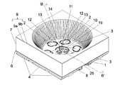
【図7−A】本発明の実施例において極性を持たない熱伝導性枠7、又は金属枠21に筐体を取付けた斜視図である。
【図7−B】図7−AのB−B’断面図である。
【図8】本発明の実施例において極性を持つ熱伝導性枠7を基板24に取付けた斜視図である。
【図9−A】本発明における該基板の第7実施例を示す斜視図である。
【図9−B】図9−AのB−B’断面図である。
【図10−A】本発明における該基板の第8実施例を示す斜視図である。
【図10−B】図10−AのB−B’断面図である。
【図11−A】本発明における該基板の第9実施例を示す斜視図である。
【図11−B】図11−AのB−B’断面図である。
【図11−C】第9実施例の熱伝導性枠7と表面電極3とをカシメにより熱伝導的な接続を行った断面図である。
【図12−A】本発明における該基板の第10実施例を示す分解図である。
【図12−B】図12−AのB−B’断面における該基板の断面図である。
【図12−C】第10実施例の熱伝導性枠7に形成された枠凹部35と表面電極3上に形成された導電性の突起28とを挿入接触させた事により熱伝導的な接続を行った事を示す断面図である。
【図13−A】本発明における該基板の第11実施例を示す分解図である。
【図13−B】図13−AのB−B’断面における該基板の断面図である。
【図13−C】第11実施例の導電性の突起28を熱伝導性枠7の底面開口部29を閉鎖するように形成し、熱伝導性枠7と表面電極3とを熱伝導的に接続を行った構造を示す断面図である。
【図14】第11実施例における変形実施例の断面図であり、(A)は熱伝導性枠7、導電性の突起28、表面電極3に金属層9が析出した状態を示し、(B)は金属層9を厚み方向に成長させた状態を示している。
【図15】第1実施例に示す金属層9の電解メッキ法による形成過程の説明のための断面図であり、(A)は熱伝導性枠7からの金属層9の成長、及び表面電極3からの金属層9の成長を示し、(B)は絶縁性の接着剤層8を金属層9が被覆した状態を示し、(C)は被覆された金属層9を厚み方向に成長させた状態を示している。
【図16−A】第1実施例の変形実施例を示す該基板の斜視図である。
【図16−B】図16−AのA−A’断面図である。
【図17−A】本発明における該基板の第12実施例の断面図である。
【図17−B】第12実施例の変形実施例の断面図である。
【図18】本発明の電子部品実装基板の第6実施例の作製工程フロー図であり、(A)は第1工程、(B)は第2工程、(C)は第3工程、(D)は第4工程、(E)は第5工程、(F)は第6工程を示す。
【図19】本発明の電子部品実装基板の第1実施例の作製工程フロー図であり、(A)は第1工程、(B)は第2工程、(C)は第3工程、(D)は第4工程を示す。
【図20−A】従来の電子部品実装基板の斜視図である。
【図20−B】図20−Aの分解図である。
【図20−C】図20−Aの断面図である。
【符号の説明】
【0036】
1 絶縁基材
2 極性を持つ表面電極(導体)
3 極性を持たない表面電極(導体)
4 極性を持つ裏面電極(導体)
5 極性を持たない裏面電極(導体)
6 回路基板
7 熱伝導性枠
8 接着剤層
9、9a、9b 金属層
10 ダイボンド樹脂又はダイボンドシート
11 LED素子(半導体素子)
12 金属細線
13 LED素子の電極
14 樹脂
15 スルホール
16、16a、16b、16c 金属表面処理層
17 絶縁性樹脂
18 半田付け部
19 LED搭載用孔
21 金属枠
22 筐体
24 基板
25 基板開口部
26 枠開口部
27 鋲
28、28a 導電性の突起
29 熱伝導性枠の底面開口部
30 金属拡散層
31 バリアメタル層
32 金属のメッキ層
33 エッチングレジスト層
34 カシメ部
35 枠凹部
36 接触部
37 デバイド部
38 ツェナー素子
101 絶縁基材
102 極性を持つ表面電極(導体)
104 極性を持つ裏面電極(導体)
106 回路基板
107 金属枠
108 接着剤層
110 ダイボンド樹脂又はダイボンドシート
111 LED素子
112 金属細線
113 LED素子の電極
114 樹脂
137 金属枠の脚部
【発明を実施するための最良の形態】
【0037】
以下に、添付図面に基づいて本発明に係わる電子部品実装基板、及び該基板の製造方法の実施例を詳細に説明する。図1−A〜図1−Cは、電子部品実装基板の第1実施例であり、図1−Aは、内部配線を透視により示した斜視図、図1−Bは、分解図、図1−Cは、図1−AのA−A’断面図で、図1−Dは、図1−AのB−B’断面図である。
【0038】
詳細に説明すると、回路基板6は、絶縁基材1の上面に複数の導体、即ち複数の正と負の極性を持つ表面電極2(以下極性を持つ表面電極2と記す)と一つ以上の極性を持たない表面電極3、及び絶縁基材1の下面に各表面電極と電気的に接続された、複数の正と負の極性を持つ裏面電極4(以下極性を持つ裏面電極4と記す)と一つ以上の極性を持たない裏面電極5が形成されている。次に該回路基板6上の、極性を持たない表面電極3上面に、熱伝導性を有する枠7(以下熱伝導性枠7と記す)を接着剤層8を用いて貼付ける。
【0039】
該熱伝導性枠7、極性を持たない表面電極3、及びこれら両者に介在する接着剤層8の表面を被覆するように金属層9(9aは熱伝導を目的とした金属層、9bは表面処理を目的とした金属層)を形成し、該枠7と該表面電極3とを金属層9により熱伝導的に接続する(図1−D参照)。更に、該回路基板6上の極性を持たない表面電極3上に、ダイボンド樹脂、又はダイボンドシート10を用いLED素子11を搭載し、金属細線12により一方のLED素子の電極13と一方の電気的な極性を持つ表面電極2を接続し、金属細線12により他方のLED素子の電極13と他方の電気的な極性を持つ表面電極2とをそれぞれ接続し、樹脂14にてLED素子11、金属細線12を封止した構造を特徴とする(図1−C参照)。
【0040】
前記、図1−A〜図1−Dによれば、LED素子11からの発熱が、極性を持たない表面電極3より金属層9を介し外気に放熱される経路を持ち、LED素子11からの発熱が効率良く外気に放熱される事と成り、LED素子11の温度上昇が抑制され、より電流量に比例した高輝度が得られ、寿命の向上が得られるものと成る。特に、熱伝導性枠7が金属体にて構成されている場合においては、熱放出の媒体となる金属の容量、及び熱放出に関与する外気との接触面が増加し、LED素子11からの発熱がより効率良く外気に放出されるものと成り、上記効果がより優れたものと成る。
【0041】
また、前記図面によれば理解できるように、回路基板6と、該熱伝導性枠7との取付けに用いられる接着剤層8の界面は金属層9により被覆されているので、光漏れが無く、表面実装型LEDとしての輝度の損失を招く問題は改善されるものとなり、且つ金属層9により該熱伝導性枠7と回路基板6が接続された構造となるので、該熱伝導性枠7と回路基板6との密着強度の向上も得られる。
【0042】
図2−A〜図2−Cは、本発明の電子部品実装基板の第2実施例であり、図2−Aは分解図、図2−Bは図2−AのA−A’断面における該基板の断面図、図2−Cは図2−AのB−B’断面における該基板の断面図である。絶縁基材1の上に形成された極性を持たない表面電極3と、極性を持つ表面電極2が回路基板6の端面に形成されたスルホール15により極性を持つ裏面電極4に電気的に接続された構造を持つ回路基板6において、該極性を持つ表面電極2上の金属細線12の接続個所を除く部分を絶縁性樹脂17にて被覆し、熱伝導性枠7と極性を持たない表面電極3を接着剤層8を用いて貼付け、金属層9を形成し、該熱伝導性枠7と該表面電極3とを金属層9により熱伝導的に接続した事を特徴としている。
【0043】
この図2−A〜図2−Cの様に、前記熱伝導性枠7下に極性を持つ表面電極2が一方、又は両方形成されている場合は、該熱伝導性枠7(ここでは金属表面を有する場合)を各表面電極とを接着剤層8のみを用いて貼付けると、該熱伝導性枠7と各表面電極との貼付け時に該熱伝導性枠7が各電極と接触(ペネトレーション)を起し短絡を起す危険性がある。且つ熱伝導性枠7と各表面電極を金属層9にて電気的に接続する際にも短絡が発生する為、極性を持つ表面電極2の一方、又は両方を予め絶縁性樹脂17にて被覆し、極性を持つ表面電極2が同時に熱伝導性枠7と接続される事を回避するので、第1実施例と同等の効果を備える事が可能と成る。
【0044】
図3−A〜図3−Cは、本発明の電子部品実装基板の第3実施例であり、図3−Aは分解図、図3−Bは、図3−AのA−A’断面図、図3−Cは図3−AのB−B’断面図である。第1実施例に示す図1−Aの熱伝導性枠7下の極性を持たない表面電極3の外周部を除く事により、円形状とした(円形で無くても良い)表面電極3を形成し、現出する絶縁基材1上に接着剤層8を塗布、又は貼付け、熱伝導性枠7を接着固定し、該枠7と該表面電極3とが接触する事により熱伝導的に接続した事を特徴としている(16a、16bは金属表面処理層である)。
【0045】
この図3−A〜図3−Cに示す様に、第1実施例の各図に見られる熱伝導性枠7と極性を持たない表面電極3の間に介在していた接着剤層8が無くなり、金属層9を形成しなくても該熱伝導性枠7と該表面電極3とが接触する事により熱伝導的に接続され、第1実施例と同等の効果が得られる。また、該表面電極3が熱圧着時における接着剤層8の枠7内への滲み出しを防ぐダム効果を有するものと成る。
【0046】
また、前記に示した表面電極3の外周部を完全に除去を行わずに段差を設け、同様の考えにて段差底部に接着剤層8を塗布、又は貼付け、前記熱伝導性枠7を接着固定しても良い(不図示)。
【0047】
また、第3実施例の該枠7と該表面電極3とを第1実施例、第2実施例に示す金属層9により熱伝導的に接続しても良く、これにより放熱効果を高める事ができる(不図示)。
【0048】
図4−A〜図4−Cは、本発明の電子部品実装基板の第4実施例であり、図4−Aは分解図、図4−Bは図4−AのA−A’断面図、図4−Cは図4−AのB−B’断面図である。回路基板6は、支持板を兼ねた正と負の極性を持つ裏面電極4、及び極性を持たない裏面電極5と、該各裏面電極を一定間隔介して並べ、この該各裏面電極を保持すると共に、LED搭載用穴19を形成し、極性を持つ裏面電極4と電気的に接続された極性を持つ表面電極2、極性を持たない表面電極3を備えたものである。次に、前記熱伝導性枠7と該表面電極3を接着剤層8を用い貼付け、該熱伝導性枠7と該表面電極3とを金属層9により熱伝導的に接続する。更に、該回路基板6の極性を持たない裏面電極5上に、ダイボンド樹脂、又はダイボンドシート10を用いLED素子11を搭載し、金属細線12によりLED素子の電極13と電気的な極性を持つ裏面電極4をそれぞれ接続し、樹脂14により封止を行なったものである。
【0049】
この図4−A〜図4−Cの様に、LED素子11を搭載する電極(ここでは極性を持たない裏面電極5)が、前記熱伝導性枠7と熱伝導的に接続されていない場合においても、LED素子11からの発熱が、間接的では有るが樹脂14を伝い、該表面電極3を介する、又は直接該熱伝導性枠7に熱伝導され、LED素子11からの発熱が効率良く外気に放出されるものとなる。
【0050】
また、図4−D、図4−Eの各断面図に示すように、LED素子11が搭載された極性を持たない裏面電極5を金属層9により、極性を持たない表面電極3に熱伝導的に接続する事により、LED素子11からの発熱がより効率的に熱伝導性枠7に熱伝導される事と成り、図4−B、図4−Cに示される構造よりも優れた放熱効果を有するものと成る。
【0051】
図5−A、図5−Bは、本発明の電子部品実装基板の第5実施例であり、図5−Aは斜視図、図5−Bは図5−AのC−C’断面図である。第1実施例に示す回路基板6上に形成していた極性を持たない表面電極3を、本実施例では形成せず、正と負の極性を持つ表面電極2を形成し、正と負の極性を持つ表面電極2のどちらか一方と熱伝導性枠7と接着剤層8を用い貼付け、金属層9を形成し、該熱伝導性枠7と該表面電極2の一方とを金属層9により電気的、熱伝導的に接続した事を特徴としている。
【0052】
この図5−A、図5−Bの様に、上記構成の電子部品実装基板上にLED素子11を実装、樹脂14により封止を行なう事により、第1実施例と同等の効果を備える事が可能と成る。
【0053】
また、図5−A、図5−Bにおいて、実装されるLED素子11が、上下面にLED素子の電極13を備える場合は、一方の極性を持つ表面電極2上に導電性を有するダイボンド樹脂、又はダイボンドシート10を用いLED素子11を搭載、下面に形成されたLED素子の電極13と接続し、他方の極性を持つ表面電極2と上面に形成されたLED素子の電極13を金属細線12により接続しても良い(不図示)。
【0054】
前記第1実施例〜第5実施例を含み、本発明における回路基板6には、絶縁基材1上に導体を形成したもの、又は該絶縁基材1上に導体を形成したものを複数層形成させたもの、又はリードフレームに絶縁材料を貼付けたもの等が用いられる。
【0055】
熱伝導性枠7は、Al(熱伝導率236W/m・K)、Fe(熱伝導率83.5W/m・K)、Cu(熱伝導率403W/m・K)、Mg(熱伝導率157W/m・K)等の金属体を主として形成されたもの、又は熱伝導率が10W/m・K未満のセラミック、絶縁性樹脂にて形成された枠の表面に金属層を付与したもの、金属体とセラミック、絶縁性樹脂の組合せにより構成される基板材料等により形成された枠の表面に金属層を付与したもの、カーボン等の導電性を有する物質にて形成された枠の表面に金属層を付与したものが用いられる。
【0056】
また、前記熱伝導率が10W/m・K未満のセラミック、絶縁性樹脂にて形成された枠、金属体とセラミック、絶縁性樹脂の組合せにより構成される基板材料等により形成された枠の表面に金属層を形成する手法としては、スパッタ法、蒸着法、電解メッキ法、無電解メッキ法等、又はいずれかの方法の組合せにより金属層を形成する事が好ましい。
【0057】
また、無電解メッキ法を用いる場合においては、セラミック、絶縁性樹脂等の絶縁性を示す枠材料に触媒を混入、又は枠の表面に付与させて用いても良い。
【0058】
また、電解メッキ法を用いる場合においては、セラミック、絶縁性樹脂等の絶縁性を示す枠材料表面にカーボン等の導電性を有する物質を付与させて用いても良い。
【0059】
また、前記Al、Fe、Cu、Mg等の金属体を主体とし形成された枠の表面に、更なる金属の表面層を前記方法にて形成しても良い。
【0060】
また、前記熱伝導性枠7の表面の金属層には、Cu(熱伝導率403W/m・K)、Ni(熱伝導率94W/m・K)、Au(熱伝導率319W/m・K)、Ag(熱伝導率428W/m・K)、Pd(熱伝導率72W/m・K)、Sn(熱伝導率68W/m・K)、Al(熱伝導率236W/m・K)、又はこれらの金属を複数積層させて用いても良い。
【0061】
また、各導体、即ち極性を持つ表面電極2、極性を持たない表面電極3、極性を持つ裏面電極4、極性を持たない裏面電極5には、Al、Fe、Cu等の金属を主体とした金属体、又は合金が用いられる。
【0062】
また、極性を持つ表面電極2、極性を持たない表面電極3、極性を持つ裏面電極4、極性を持たない裏面電極5の各表面には、Cu、Ni、Au、Ag、Pd、Snメッキやこれらを複数積層させたメッキを行う事が好ましい。
【0063】
また、金属層9にはCu、Ni、Au、Ag、Pd、Snメッキやこれらを複数積層させたメッキを行う事が好ましい。
【0064】
また、第3実施例に図示されているように、該熱伝導性枠7と該表面電極3とが接触する事により熱伝導的に接続される構造においては、前記金属層9を形成する必要性が無い事から、熱伝導性枠7には、熱伝導率が10W/m・K以上のセラミック、絶縁性樹脂により構成されたもの、又は、Alを用いた枠の表面にアルマイト層(熱伝導率80W/m・K)を形成したもの等も用いられる。
【0065】
また、金属細線12には、Ag、Au、Al等などの金属が用いられる。
【0066】
また、ダイボンド樹脂には、エポキシ樹脂、エポキシ樹脂等にAu、Ag、Cuなどの金属や半田等の合金、ITO、SnO2などの金属酸化物の導電性材料を混合して作られたペーストが用いられ、ダイボンドシートにはエポキシ樹脂のシート等が用いられる。
【0067】
また、LED素子11、金属細線12の封止に用いられる樹脂14には透光性樹脂、又は蛍光体樹脂が用いられる。
【0068】
図6−A〜図6−Cは、本発明の電子部品実装基板の第6実施例であり、図6−Aは斜視図、図6−Bは図6−AのA−A’断面図、図6−Cは図6−AのB−B’断面図である。第1実施例を示す図の回路基板6上に、メッキ法により析出せしめた金属層にて金属枠21を形成し、該金属枠21と該表面電極3とが熱伝導的に接続された一体構造を特徴とするものである(16cは金属表面処理層、31はバリアメタル層である)。
【0069】
前記、図6−A〜図6−Cによれば、回路基板6上の、該金属枠21と該表面電極3とが熱伝導的に接続された一体構造を有する為、接着剤層8の必要性が無く、第1実施例と同様の効果を備えるものと成っている。
【0070】
また、金属枠21には、Cu、Ni、Au、Ag、Pd、Sn、又は、これらの金属を複数積層させて用いる事が好ましい。
【0071】
前記第1実施例〜第4実施例及び第6実施例に用いた各図は、該熱伝導性枠7及び金属枠21が極性を持たないものと成っており、他の導電性を有するものと接触しても、電気的な短絡を起こす可能性が無い為、図7−Aの斜視図、図7−Bの断面図に示すように、該熱伝導性枠7及び金属枠21を筐体22に取付ける事も可能となる。これにより、LED素子11からの発熱が、該熱伝導性枠7及び金属枠21を介して、より大きな放熱体である筐体22に熱伝導され、さらに効率良く外気に放熱される事となる。
【0072】
前記第5実施例に用いた各図は、回路基板6の極性を持つ表面電極2と熱伝導性枠7が電気的、熱伝導的に接続されている事により、熱伝導性枠7が極性を持つものと成っており、該熱伝導性枠7がLED素子11を発光させる為の電極機能を有し、図8に示すように表面実装型LEDとして実装される場合において、基板24上の接続端子として用いる事も可能となる。
【0073】
図9−A、図9−Bは、本発明の電子部品実装基板の第7実施例であり、図9−Aは斜視図、図9−Bは図9−AのB−B’断面図である。図9−Aは、第4実施例に示す各図にて説明を行なった回路基板6に、基板開口部25を設け、前記熱伝導性枠7と前記極性を持たない電極3を接着剤層8を用い貼付け、該熱伝導性枠7と該極性を持たない裏面電極5とを該基板開口部25に形成された金属層9を介して熱伝導的に接続した事を特徴としたものである。
【0074】
この図9−A、図9−Bの様に、基板開口部25を設ける事により、回路基板6に形成された如何なる導体においても、該基板開口部25に形成された金属層9を介して該熱伝導性枠7と熱伝導的に接続することが可能となる。
【0075】
図10−A、図10−Bは、本発明の電子部品実装基板の第8実施例であり、図10−Aは斜視図、図10−Bは図10−AのB−B’断面図である。このように、第7実施例の図9−A、図9−Bに示す基板開口部25上の熱伝導性枠7に、枠開口部26を設け、基板開口部25、枠開口部26を熱伝導的に接続しても良い。
【0076】
また、基板開口部25に形成された金属層9の替わりに、導電性、及び熱伝導性の機能を有する金属体、又は金属ペーストを用いても良い。
【0077】
図11−A、図11−Bは、本発明の電子部品実装基板の第9実施例であり、図11−Aは斜視図、図11−Bは図11−AのB−B’断面図である。このように、第1実施例と同じ回路基板6上の極性を持たない表面電極3に鋲27により熱伝導性枠7を取付け、該熱伝導性枠7と該表面電極3とを熱伝導的に接続した事を特徴とするものである(16は金属表面処理層である)。
【0078】
この図11−A、図11−Bに示す構成であれば、表面電極3上の熱伝導性枠7を機械的に接続している事から、第1実施例に見られる接着剤層8の必要性が無く、熱伝導性枠7と表面電極3とを金属層9にて熱伝導的に接続する必要性は省かれ、第1実施例と同様の効果を備えるものと成っている。
【0079】
また、接続が機械的に行われている為、回路基板6と熱伝導性枠7の密着強度が、第1実施例の構成と比較して非常に高い密着強度が得られる。
【0080】
また、金属製の鋲27を用いる事により、裏面電極5から金属製の鋲27を介して該熱伝導性枠7に熱伝導されるものと成り、裏面電極5にLED素子11が搭載された場合においても、LED素子11からの発熱が裏面電極5から金属製の鋲27を介して熱伝導性枠7に熱伝導されるものと成る。
【0081】
また、図11−Cの断面図は、表面電極3上の熱伝導性枠7が機械的に接続された別の実施例であり、表面電極3の外周部にカシメ部34を形成し、表面電極3と熱伝導性枠7とを熱伝導的に接続したものである。また、このカシメ部34にて密着強度が得られる場合においては接着剤層8は用いなくても良い。
【0082】
また、機械的な接続には、ボルト、ねじ込み等も含まれる。
【0083】
図12−A、図12−Bは、本発明の電子部品実装基板の第10実施例であり、図12−Aは分解図、図12−Bは図12−AのB−B’断面における電子部品実施基板の断面図である。このように、回路基板6上の極性を持たない表面電極3に、導電性の突起28を形成し、該突起28の上面が被覆されないように、接着剤層8を設けた後、熱伝導性枠7を取付け、該熱伝導性枠7と該突起28の上面が接触、固定される事により、該熱伝導性枠7と該表面電極3とを該突起28を介して電気的、熱伝導的に接続した事を特徴とするものである。
【0084】
上記構成により、LED素子11からの発熱が効率良く外気に放熱されるものと成る。
【0085】
導電性の突起28には、Ni、Au、Ag、Cu、Al等の金属体、半田等の合金、或いは、導電性材料(Au、Ag、Cu、Al等の金属、半田等の合金、ITO、SnO2などの金属酸化物)を樹脂に混合して作られた導電ペースト、カーボン素材等を用いた高熱伝導性材料等が用いられる。
【0086】
また、図12−Cの断面図に示すように、熱伝導性枠7に枠凹部35を周囲、又は部分的に形成し、該凹部35に突起28を差込み、接触部36により熱伝導的に接続させても良い。この構造によれば、前記回路基板6と該熱伝導性枠7が接着剤層8により接着固定される工程において、回路基板6と熱伝導性枠7が精度良く貼付けられる事が可能と成る。
【0087】
また、接触部36の機械的な接続強度が所定の強度を満たすものであれば、接着剤層8は無くても良い。
【0088】
図13−A、図13−Bは、本発明の電子部品実装基板の第11実施例であり、図13−Aは分解図、図13−Bは図13−AのB−B’断面における該電子部品実装基板の断面図である。この図13−A、図13−Bは、導電性の突起28を、熱伝導性枠7の底面開口部29の周囲に円形状に形成した事を特徴としている(28aは外周囲に形成した導電性突起である)。
【0089】
上記突起28は、前記熱伝導性枠7の底面開口部29の周囲に形成した事により、LED素子11から発せられる光が、該突起28により遮光される。
【0090】
また、上記突起28は、熱伝導性枠7と回路基板6とを接着剤層8で貼付ける際の、加熱圧着による接着剤層8の滲み出しを防ぐ効果も備えており、この接着剤層8の滲み出しによる、LED素子11搭載部、及び接続する各表面電極の汚染の発生を低減させ、更に工程内での接着剤層8の厚み条件、及び該枠7と回路基板6とを貼付ける際の加熱圧着条件等の管理範囲が広くなり、品質的にも安定し歩留まりの向上効果も有する。
【0091】
熱伝導性枠7の底面開口部29の周囲に形成された導電性の突起28の形状は、図13−A、図13−Bに示す円形状に限らず、角型、その他異形状にて底面開口部29の周囲に形成しても良い。
【0092】
また、図13−Cに示すように、導電性の突起28を底面開口部29を閉鎖するように形成しても良く、この場合における突起28の形成には、電解メッキ法、無電解メッキ法によりNi、Au、Ag、Cu等の金属が用いられ、底面開口部29の内部に形成されている各電極もメッキ法にて形成される金属により被覆され導体体積が増し、LED素子11からの発熱を、より効率良く熱伝導性枠7に伝える事が可能と成る。
【0093】
図14は、第11実施例の変形実施例であり、熱伝導性枠7、導電性の突起28、導体3(極性を持たない表面電極3)を金属層9により熱伝導的に接続している構成を示しており、金属層9は、通常電解メッキ法を用いて形成される。図14(A)は、熱伝導性枠7、導電性の突起28、表面電極3にそれぞれ金属層9が析出し、連続した金属層9を形成している。図14(B)は金属層9を厚み方向に成長させて熱伝導性枠7と表面電極3の熱伝導的な接続を確実にしている。図15は、第1実施例に示す金属層9の電解メッキ法による形成過程の説明図である。
【0094】
熱伝導性枠7、及び極性を持たない表面電極3に給電を行い(表面電極2に給電しても良い)図15(A)に示すように熱伝導性枠7からの金属層9の成長、及び該表面電極3からの金属層9の成長が開始され、次に図15(B)に示すように絶縁性の接着剤層8を金属層9が被覆し、更に図15(C)に示すように被覆された金属層9を厚み方向に成長させ、熱伝導性枠7と該表面電極3の熱伝導的な接続を確実にしている。図14に示す実施例によれば第1実施例のように熱伝導性枠7からの金属層9の成長、及び表面電極3からの金属層9の成長による金属層9の一体化に頼らずとも、熱伝導性枠7と導電性の突起28と表面電極3のそれぞれの金属層9による接続が可能と成り、電解メッキ工程の時間短縮効果、及びより高い放熱効果を得る事が可能と成る。
【0095】
また、図16−A、図16−Bは、第1実施例の変形実施例を示し、熱伝導性枠7と熱伝導的に接続されていない極性を持つ表面電極2に金属層9を形成せず、金属層9の厚み分低く段差を設けてツェナー素子38を表面電極2上に搭載している。よって、LED素子11から発せられる光がツェナー素子38により遮光されず、効率良く光が該枠7上の金属層9bに照射され効率良く上方に出射される。また、金属層9の厚みが増す事により放熱性も向上する。
【0096】
図17−Aは、本発明の電子部品実装基板の第12実施例の断面図である。このように第1実施例の回路基板6上の極性を持たない表面電極3と、熱伝導性枠7を溶接により、該熱伝導性枠7上の金属表面処理層16と該表面電極3とを金属拡散層30を形成し熱伝導的に接続した事を特徴としている。
【0097】
上記構成によれば、第1実施例に見られる接着剤層8の必要性が無く、金属層9にて熱伝導的に接続する必要性は省かれ、且つ、第1実施例と同様の効果を備えるものと成る。
【0098】
また、前記熱伝導性枠7と前記表面電極3との接続が、金属拡散層30による金属結合による為、回路基板6と熱伝導性枠7の密着強度が、非常に高く成る。
【0099】
また、溶接による接続方法としては、アーク溶接、電子ビーム溶接等の電気的エネルギーを用いる溶接法、及び半田を含むろう付け等による化学的エネルギーを用いる溶接法、及び圧接等による機械的エネルギーを用いる溶接法、及び超音波溶接法、レーザー溶接法等が用いられる。
【0100】
また、第11実施例にて示されている図13−A、図13−Bの接着剤層8に変えて半田を用いる事により、熱伝導性枠7の底面開口部29の周囲に形成した導電性の突起28が、半田溶融時における各電極への半田の流れ出し防止用ダムとしての効果を持つ。
【0101】
また、前記に示す熱伝導性枠7の底面開口部29の周囲に形成した導電性の突起28を接着剤層8に変え、半田を同様の位置に設け、接着剤層8にて熱伝導性枠7を仮固定した後、半田溶融を行い、熱伝導性枠7と表面電極3とを溶接し、熱伝導性枠7と表面電極3とを熱伝導的に接続しても良い(不図示)。
【0102】
また、該熱伝導性枠7と該表面電極3の溶接は、全面的、又は部分的に行っても良い。
【0103】
また、図17−Bは第12実施例の変形実施例の断面図を示しており、極性を持たない表面電極3により閉鎖された基板開口部25が設けられた回路基板6を用い、基板開口部25を閉鎖した部分の極性を持たない表面電極3と熱伝導性枠7とを前記溶接法を用い部分的に溶接し、熱伝導的に接続しても良い。
【0104】
また、本発明の第10実施例で示す導電性の突起28が、Au、Ag、Cu、Alなどの金属や半田等の合金で形成される場合には、前記にて説明を行ったいずれかの溶接法を用い、導電性の突起28の上面と熱伝導性枠7間に金属拡散層30を形成させ、金属的に接合する事も可能である。この場合、導電性の突起28の上面と熱伝導性枠7の接合強度が付加される。
【0105】
以上本発明の電子部品実装基板について種々の実施例について説明したが、熱伝導性枠7、又は金属枠21の形状、及び内壁角度、高さにおいては使用目的に応じて設定し用いる事が好ましく、必要に応じ多段構造にする事、金属枠21の上面に熱伝導性枠7を重ねて熱伝導的に接続する事なども可能である。
【0106】
また、これらに限らず、それぞれの目的に応じて、前記第1実施例〜第12実施例に示した構造を適宜組み合わせて用いる事ができる。
【0107】
以下に、本発明の電子部品実装基板の製造方法の実施例について説明する。
【0108】
図18は、第6実施例に示す構造の電子部品実装基板の代表的な作製工程フローを部分的に示した、電気的接続を示したA−A’部、及び熱伝導的な接続を示したB−B’部の合成断面図である。工程1として、図18の(A)のように、絶縁基材1の上面に複数の導体、即ち極性を持つ表面電極2と極性を持たない表面電極3、及び絶縁基材1の下面に各表面電極と電気的に接続された、極性を持つ裏面電極4と極性を持たない裏面電極5が形成された回路基板6を作製する。工程2として、図18の(B)のように、回路基板6に形成された各電極を全面被覆するようにバリアメタル層31を形成する。工程3として、図18(C)のようにバリアメタル層31を含む全面に、更なる金属のメッキ層32をメッキ法により形成する。工程4として、図18(D)のように、金属のメッキ層32上に枠形成用、及び各裏面電極形成用のマスク層であるエッチングレジスト層33を形成する。工程5として、図18(E)のように、金属のメッキ層32に対し腐食性を持ち、バリアメタル層31に対し腐食性を持たないエッチング液を用い、金属のメッキ層32をエッチングし金属枠21、及び各裏面電極を形成する。工程6として、図18(F)のように、エッチングレジスト層33の除去を行なう。
【0109】
図18(A)〜図18(F)に示す工程を用いる事により、第6実施例の金属枠21と該表面電極3とが熱伝導的に接続された一体構造を特徴とする本発明の電子部品実装基板を作製する事が可能となる。
【0110】
また、図18(B)に示すバリアメタル層31には、金属のメッキ層32をエッチングするときに腐食性を持たない(耐エッチング性のある)別の金属を用いる事が好ましく、Au、Ni又はPb−Zn等の半田合金、Ni−Au合金等が用いられる。
【0111】
また、バリアメタル層31の形成においては、電解メッキ法、無電解メッキ法が用いられる。
【0112】
また、金属のメッキ層32に用いられる金属としては、Cuが用いられ、電解メッキ法、無電解メッキ法により形成される。
【0113】
また、エッチング液は、金属のメッキ層32にCu、バリアメタル層31に前記記載の物質が用いられる場合において、アルカリエッチング液、過硫酸アンモニウム溶液、過酸化水素と硫酸の混合溶液等が使用される。
【0114】
また、図18(F)に示す工程6以後の工程として、エッチング工程において部分的に露出した各電極を被覆しているバリアメタル層31は、除去、又は除去しなくても良い。
【0115】
また、前記工程にて形成された各電極、及び金属枠21には、Cu、Ni、Au、Ag、Pd、Snメッキやこれらを複数積層させたメッキを行う事が好ましい。
【0116】
図19は、第1実施例に示す構造の本発明電子部品実装基板の代表的な作製工程フローを部分的に示した、電気的接続を示したA−A’部、及び熱伝導的な接続を示したB−B’部の合成断面図である。工程1として、図19(A)のように、絶縁基材1の上面に複数の導体、即ち極性を持つ表面電極2と極性を持たない表面電極3、及び絶縁基材1の下面に各表面電極と電気的に接続された、極性を持つ裏面電極4と極性を持たない裏面電極5が形成された回路基板6を作製する。工程2として、図19(B)のように、極性を持たない表面電極3上の熱伝導性枠7取付け部分に接着剤層8を設ける。工程3として、図19(C)のように、熱伝導性枠7を、極性を持たない表面電極3上の熱伝導性枠7取付け部分に接着剤層8を介して貼付ける。工程4として、図19(D)のように、電解メッキ法を用い各電極、熱伝導性枠7、及び極性を持たない表面電極3と熱伝導性枠7間に介在する接着剤層8の露出部分に金属層9を形成し、極性を持たない表面電極3と熱伝導性枠7を金属層9により熱伝導的に接続する。
【0117】
前記図19(A)〜図19(D)に示す工程を用いる事により、第1実施例の熱伝導性枠7と該表面電極3とが熱伝導的に接続された事を特徴とする本発明の電子部品実装基板を作製する事が可能となる。
【0118】
また、工程2を示す図19(B)では、極性を持たない表面電極3上の熱伝導性枠7取付け部分に接着剤層8を設けているが、熱伝導性枠7の底部、又は極性を持たない表面電極3上と熱伝導性枠7の底部の両方に接着剤層8を設けても良い。
【0119】
また、前記と同様に絶縁基材1上に熱伝導性枠7の取付け部分がある場合は、絶縁基材1上、又は熱伝導性枠7の底部、又は絶縁基材1上と熱伝導性枠7の底部の両方に接着剤層8を設けても良い。
【0120】
また、前記各実施例は、図示の通り本発明の電子部品実装基板を一個体にて説明しているが、製品の仕様において複数を連結させた構造とする事も可能である。
【0121】
要は、回路基板6が複数の連結構造を取り、取付けられる熱伝導性枠7も複数の連結構造、又は回路基板6が複数の連結構造を取り、取付けられる熱伝導性枠7が一個体、又は回路基板6が一個体、取付けられる熱伝導性枠7が複数の連結構造の、いずれの構成においても本発明は適応可能となる。
【0122】
また、回路基板6上にLED素子11を実装後、樹脂14にて封止を行ったものに、熱伝導性枠7を取付け、回路基板6に形成されたいずれかの導体と該熱伝導性枠7を熱伝導的に接続する事も本発明においては適応可能となる。【Technical field】
[0001]
The present invention relates to an electronic component mounting substrate and a method for manufacturing the substrate, and more particularly to an electronic component mounting substrate suitable for a surface mount LED and a method for manufacturing the substrate.
[Background]
[0002]
As the electronic component mounting substrate, as shown in FIGS. 20A to 20C, a
[0003]
[Patent Document 1]
JP 2005-229003 A
DISCLOSURE OF THE INVENTION
[Problems to be solved by the invention]
[0004]
The above-described conventional electronic component mounting board heats the light emitted from the
[0005]
In addition, the
[0006]
Accordingly, an object of the present invention is to provide an electronic component mounting board characterized by a structure that solves the above problems, and a method of manufacturing the board.
Means for solving the problem
[0007]
The invention of
[0009]
The invention of
The invention of
According to a fourth aspect of the present invention, on the upper surface of the surface electrode for mounting a semiconductor element, Above Protrusion Multiple It is characterized by being formed.
According to a fifth aspect of the present invention, on the upper surface of the surface electrode for mounting a semiconductor element, Above Protrusion In a ring It is formed.
[0020]
The electronic component mounting board according to the first aspect of the present invention is a semiconductor element mounting board in which heat generated from a semiconductor element is formed on a circuit board. Surface electrode Through the frame with thermal conductivity body The semiconductor element is thermally conducted directly or indirectly, and is dissipated from the surface of the frame to the outside air, thereby suppressing the temperature rise of the semiconductor element. In particular, in the surface mount type LED, the temperature rise of the LED element is suppressed, and high brightness and an improvement in the life in proportion to the amount of current can be obtained. Furthermore, in the area where the adhesive is interposed, the adhesion strength between the circuit board and the frame can be secured, and the frame body And semiconductor device mounting Surface electrode In the area where the body And semiconductor device mounting Surface electrode An electrical and heat conductive connection between them is ensured. Therefore, the heat generated from the semiconductor element is used for mounting the semiconductor element. Surface electrode Conducted to the front frame body And semiconductor device mounting Surface electrode Frame in the area where the body Therefore, the LED element is prevented from rising in temperature, and high brightness and an improvement in life are obtained in proportion to the amount of current.
[Brief description of the drawings]
[0035]
1A is a perspective view showing an internal wiring according to a first embodiment of an electronic component mounting board of the present invention.
FIG. 1-B is an exploded view of FIG. 1-A showing a first embodiment of the present invention.
1-C is a cross-sectional view taken along the line AA ′ of FIG. 1-A.
1-D is a cross-sectional view taken along the line BB ′ of FIG. 1-A.
FIG. 2-A is an exploded view showing a second embodiment of the substrate according to the present invention.
2B is a cross-sectional view of the substrate taken along the line AA ′ of FIG.
FIG. 2-C is a cross-sectional view of the substrate taken along the line BB ′ of FIG. 2-A.
FIG. 3-A is an exploded view showing a third embodiment of the substrate in the present invention.
FIG. 3-B is a cross-sectional view of the substrate taken along the line AA ′ of FIG. 3-A.
FIG. 3-C is a cross-sectional view of the substrate taken along the line BB ′ of FIG. 3-A.
FIG. 4-A is an exploded view showing a fourth embodiment of the substrate according to the present invention.
FIG. 4-B is a cross-sectional view of the substrate taken along the line AA ′ of FIG. 4-A.
FIG. 4-C is a cross-sectional view of the substrate taken along the line BB ′ of FIG. 4-A.
FIG. 4-D is a cross-sectional view showing that the
FIG. 4-E is a cross-sectional view showing that the
FIG. 5-A is a perspective view showing a fifth embodiment of the substrate in the present invention.
5B is a cross-sectional view taken along the line CC ′ of FIG.
FIG. 6A is a perspective view showing a sixth embodiment of the substrate in the present invention.
6B is a cross-sectional view taken along the line AA ′ of FIG. 6A.
6C is a cross-sectional view taken along the line BB ′ of FIG. 6A.
7A is a perspective view in which a housing is attached to the heat
7-B is a cross-sectional view taken along the line BB ′ of FIG. 7-A.
FIG. 8 is a perspective view in which a thermally
FIG. 9-A is a perspective view showing a seventh embodiment of the substrate in the present invention.
9-B is a cross-sectional view taken along the line BB ′ of FIG. 9-A.
FIG. 10-A is a perspective view showing an eighth embodiment of the substrate in the present invention.
10-B is a cross-sectional view taken along the line BB ′ of FIG. 10-A.
FIG. 11-A is a perspective view showing a ninth embodiment of the substrate in the present invention.
11-B is a cross-sectional view taken along the line BB ′ of FIG. 11-A.
FIG. 11C is a cross-sectional view in which the heat
FIG. 12-A is an exploded view showing a tenth embodiment of the substrate in the present invention.
12-B is a cross-sectional view of the substrate taken along the line BB ′ of FIG. 12-A.
FIG. 12-C shows a heat conductive connection by inserting and contacting the
FIG. 13-A is an exploded view showing an eleventh embodiment of the substrate in the present invention.
FIG. 13-B is a cross-sectional view of the substrate taken along the line BB ′ of FIG. 13-A.
FIG. 13-C shows that the
FIG. 14 is a cross-sectional view of a modified example of the eleventh example, in which (A) shows a state in which a
15 is a cross-sectional view for explaining the formation process of the
FIG. 16A is a perspective view of the substrate showing a modified embodiment of the first embodiment.
16-B is a cross-sectional view taken along the line AA ′ of FIG. 16-A.
FIG. 17-A is a cross-sectional view of a twelfth embodiment of the substrate in the present invention.
FIG. 17-B is a cross-sectional view of a modified example of the twelfth example.
FIGS. 18A and 18B are manufacturing process flow diagrams of a sixth embodiment of an electronic component mounting board according to the present invention, where FIG. 18A is a first process, FIG. 18B is a second process, FIG. 18C is a third process, and FIG. ) Shows the fourth step, (E) shows the fifth step, and (F) shows the sixth step.
FIGS. 19A and 19B are manufacturing process flow diagrams of the first embodiment of the electronic component mounting substrate of the present invention, where FIG. 19A is the first process, FIG. 19B is the second process, FIG. 19C is the third process, and FIG. ) Shows the fourth step.
FIG. 20A is a perspective view of a conventional electronic component mounting board.
20-B is an exploded view of FIG. 20-A.
20-C is a cross-sectional view of FIG. 20-A.
[Explanation of symbols]
[0036]
1 Insulating substrate
2 Surface electrode (conductor) with polarity
3 Non-polar surface electrode (conductor)
4 Back electrode with polarity (conductor)
5 Non-polar back electrode (conductor)
6 Circuit board
7 Thermally conductive frame
8 Adhesive layer
9, 9a, 9b Metal layer
10 Die bond resin or die bond sheet
11 LED elements (semiconductor elements)
12 Fine metal wire
13 Electrode of LED element
14 resin
15 Through Hole
16, 16a, 16b, 16c Metal surface treatment layer
17 Insulating resin
18 Soldering part
19 LED mounting hole
21 metal frame
22 Case
24 Substrate
25 Substrate opening
26 Frame opening
27 鋲
28, 28a Conductive protrusion
29 Bottom opening of thermally conductive frame
30 Metal diffusion layer
31 Barrier metal layer
32 Metal plating layer
33 Etching resist layer
34 Caulking club
35 Frame recess
36 Contact area
37 Divide Club
38 Zener element
101 Insulating substrate
102 Surface electrode with polarity (conductor)
104 Back electrode with polarity (conductor)
106 Circuit board
107 metal frame
108 Adhesive layer
110 Die bond resin or die bond sheet
111 LED elements
112 Fine metal wire
113 Electrode of LED element
114 resin
137 Leg of metal frame
BEST MODE FOR CARRYING OUT THE INVENTION
[0037]
Embodiments of an electronic component mounting board and a method for manufacturing the board according to the present invention will be described below in detail with reference to the accompanying drawings. 1-A to 1-C show a first embodiment of an electronic component mounting board. FIG. 1-A is a perspective view showing internal wiring in perspective, FIG. 1-B is an exploded view, FIG. -C is a cross-sectional view taken along the line AA 'in FIG. 1-A, and FIG. 1-D is a cross-sectional view taken along the line BB' in FIG.
[0038]
More specifically, the
[0039]
A metal layer 9 (9a is a metal layer for the purpose of heat conduction, 9b is a surface so as to cover the surface of the heat
[0040]
1A to 1D, the
[0041]
Further, as can be understood from the drawings, the interface between the
[0042]
2A to 2C show a second embodiment of the electronic component mounting board according to the present invention, FIG. 2-A is an exploded view, and FIG. 2-B is an AA ′ cross section of FIG. 2-A. FIG. 2C is a cross-sectional view of the substrate taken along the line BB ′ of FIG. 2-A. The
[0043]
As shown in FIGS. 2A to 2C, when one or both of the
[0044]
FIGS. 3A to 3C show a third embodiment of the electronic component mounting board according to the present invention, FIG. 3-A is an exploded view, and FIG. 3-B is an AA ′ cross section of FIG. 3-A. FIG. 3C is a cross-sectional view taken along the line BB ′ of FIG. By removing the outer peripheral portion of the
[0045]
As shown in FIGS. 3A to 3C, the
[0046]
Further, a step is provided without completely removing the outer peripheral portion of the
[0047]
Further, the
[0048]
4A to 4C show a fourth embodiment of the electronic component mounting board according to the present invention. FIG. 4-A is an exploded view, and FIG. 4-B is a cross-sectional view taken along line AA ′ of FIG. FIG. 4-C is a sectional view taken along the line BB ′ of FIG. 4-A. The
[0049]
When the electrode (here, the
[0050]
Further, as shown in each of the cross-sectional views of FIGS. 4-D and 4-E, the
[0051]
5A and 5B show a fifth embodiment of the electronic component mounting board according to the present invention. FIG. 5-A is a perspective view, and FIG. 5-B is a cross-sectional view along CC ′ in FIG. It is. The
[0052]
As shown in FIGS. 5A and 5B, the
[0053]
Further, in FIG. 5A and FIG. 5B, when the
[0054]
In the first to fifth embodiments, the
[0055]
The thermal
[0056]
In addition, the surface of a frame formed of a ceramic material having a thermal conductivity of less than 10 W / m · K, a frame formed of an insulating resin, a substrate material formed of a combination of a metal body and a ceramic, and an insulating resin. As a method for forming a metal layer, it is preferable to form the metal layer by a sputtering method, a vapor deposition method, an electrolytic plating method, an electroless plating method, or a combination of any of the methods.
[0057]
In the case where the electroless plating method is used, a catalyst may be mixed in a frame material showing insulating properties such as ceramic or insulating resin, or may be applied to the surface of the frame.
[0058]
In the case of using the electrolytic plating method, a conductive material such as carbon may be applied to the surface of the frame material exhibiting insulating properties such as ceramic and insulating resin.
[0059]
Further, a further metal surface layer may be formed on the surface of the frame formed mainly of the metal body such as Al, Fe, Cu, and Mg by the above method.
[0060]
The metal layer on the surface of the thermal
[0061]
Each conductor, that is, the
[0062]
Further, on each surface of the
[0063]
The
[0064]
Further, as shown in the third embodiment, the
[0065]
Further, for the
[0066]
The die bond resin is a paste made by mixing an epoxy resin, an epoxy resin or the like with a metal such as Au, Ag, or Cu, an alloy such as solder, or a metal oxide conductive material such as ITO or SnO2. An epoxy resin sheet or the like is used as the die bond sheet.
[0067]
Further, a translucent resin or a phosphor resin is used as the
[0068]
6A to 6C show a sixth embodiment of the electronic component mounting board according to the present invention. FIG. 6A is a perspective view, and FIG. 6B is a cross-sectional view taken along line AA ′ of FIG. 6C is a cross-sectional view taken along the line BB ′ of FIG. 6A. A
[0069]
According to FIGS. 6-A to 6-C, since the
[0070]
The
[0071]
In the drawings used in the first to fourth embodiments and the sixth embodiment, the heat
[0072]
Each figure used in the fifth embodiment shows that the
[0073]
9A and 9B show a seventh embodiment of the electronic component mounting board according to the present invention, FIG. 9A is a perspective view, and FIG. 9B is a cross-sectional view along BB ′ in FIG. 9A. It is. FIG. 9A shows a
[0074]
As shown in FIGS. 9A and 9B, by providing the
[0075]
10A and 10B show an eighth embodiment of the electronic component mounting board according to the present invention. FIG. 10A is a perspective view, and FIG. 10B is a cross-sectional view taken along line BB ′ of FIG. It is. Thus, the
[0076]
Further, instead of the
[0077]
11A and 11B show a ninth embodiment of an electronic component mounting board according to the present invention, FIG. 11A is a perspective view, and FIG. 11B is a cross-sectional view along BB ′ in FIG. It is. As described above, the heat
[0078]
In the structure shown in FIGS. 11A and 11B, since the heat
[0079]
Further, since the connection is mechanically performed, the adhesion strength between the
[0080]
In addition, by using the
[0081]
11C is another example in which the thermal
[0082]
The mechanical connection also includes bolts, screwing and the like.
[0083]
12A and 12B show a tenth embodiment of the electronic component mounting board according to the present invention. FIG. 12A is an exploded view and FIG. 12B is a cross-sectional view taken along the line BB ′ of FIG. It is sectional drawing of an electronic component implementation board | substrate. As described above, the
[0084]
With the above configuration, the heat generated from the
[0085]
The
[0086]
Further, as shown in the cross-sectional view of FIG. 12-C, a
[0087]
Further, the
[0088]
13A and 13B show an eleventh embodiment of the electronic component mounting board according to the present invention. FIG. 13A is an exploded view and FIG. 13B is a cross-sectional view taken along the line BB ′ of FIG. It is sectional drawing of this electronic component mounting board. 13A and 13B are characterized in that the
[0089]
Since the
[0090]
Further, the
[0091]
The shape of the
[0092]
Further, as shown in FIG. 13-C, the
[0093]
FIG. 14 shows a modified example of the eleventh embodiment in which the heat
[0094]
Power is supplied to the heat
[0095]
FIGS. 16A and 16B show a modified embodiment of the first embodiment, in which the
[0096]
FIG. 17A is a cross-sectional view of the twelfth embodiment of the electronic component mounting board according to the present invention. Thus, the
[0097]
According to the above configuration, there is no need for the
[0098]
Further, since the connection between the thermal
[0099]
In addition, as a connection method by welding, a welding method using electrical energy such as arc welding or electron beam welding, a welding method using chemical energy by brazing including solder, or mechanical energy by pressure welding or the like is used. A welding method, an ultrasonic welding method, a laser welding method, or the like is used.
[0100]
Further, by using solder instead of the
[0101]
Further, the
[0102]
Further, welding of the heat
[0103]
FIG. 17B shows a cross-sectional view of a modified example of the twelfth embodiment, using a
[0104]
Further, when the
[0105]
Although various embodiments of the electronic component mounting substrate of the present invention have been described above, it is preferable to set and use the shape, inner wall angle, and height of the heat
[0106]
In addition to the above, the structures shown in the first to twelfth embodiments can be used in appropriate combinations according to the respective purposes.
[0107]
Below, the Example of the manufacturing method of the electronic component mounting board | substrate of this invention is described.
[0108]
FIG. 18 partially shows a typical manufacturing process flow of the electronic component mounting substrate having the structure shown in the sixth embodiment, showing an AA ′ portion showing an electrical connection and a heat conductive connection. It is the synthetic | combination sectional drawing of a BB 'part. As
[0109]
By using the steps shown in FIGS. 18 (A) to 18 (F), the
[0110]
In addition, it is preferable to use another metal that does not have corrosiveness (etching resistance) when etching the
[0111]
In forming the
[0112]
The metal used for the
[0113]
Further, as the etching solution, when the Cu is used for the
[0114]
In addition, as a step after
[0115]
Moreover, it is preferable to perform Cu, Ni, Au, Ag, Pd, Sn plating and plating which laminated these two or more to each electrode formed in the said process and the
[0116]
FIG. 19 is a partial view of a typical manufacturing process flow of the electronic component mounting substrate of the present invention having the structure shown in the first embodiment, showing the AA ′ portion showing the electrical connection, and the heat conductive connection. It is the synthetic | combination sectional drawing of the BB 'part which showed. As
[0117]
A book characterized in that the heat
[0118]
Further, in FIG. 19B showing the
[0119]
Further, in the same manner as described above, when there is an attachment portion of the heat
[0120]
In each of the above embodiments, the electronic component mounting substrate of the present invention is described as a single unit as shown in the drawing, but a structure in which a plurality of units are connected in the specification of the product can also be used.
[0121]
In short, the
[0122]
Further, after mounting the
Claims (6)
前記半導体素子実装用表面電極の上面には、平坦な上面を有する導電性の突起が形成され、
該突起の上面が、前記枠体の下面に接し、
前記半導体素子実装用表面電極の上面で前記突起が形成されていない領域と、前記枠体の下面との間に、接着剤層が介在している事を特徴とする電子部品実装基板。A frame body having thermal conductivity is disposed on the upper surface side of the circuit board on which the plurality of surface electrodes are formed, and a semiconductor element is mounted on the lower surface of the frame body and the plurality of surface electrodes on the circuit board. In the electronic component mounting substrate facing a part of the upper surface of the surface electrode for mounting the semiconductor element,
Conductive protrusions having a flat upper surface are formed on the upper surface of the semiconductor element mounting surface electrode,
The upper surface of the protrusion is in contact with the lower surface of the frame,
An electronic component mounting board, wherein an adhesive layer is interposed between a region where the protrusion is not formed on the upper surface of the surface electrode for mounting a semiconductor element and the lower surface of the frame.
Priority Applications (1)
| Application Number | Priority Date | Filing Date | Title |
|---|---|---|---|
| JP2007546454A JP5074201B2 (en) | 2005-11-24 | 2006-11-22 | Electronic component mounting board |
Applications Claiming Priority (4)
| Application Number | Priority Date | Filing Date | Title |
|---|---|---|---|
| JP2005339055 | 2005-11-24 | ||
| JP2005339055 | 2005-11-24 | ||
| JP2007546454A JP5074201B2 (en) | 2005-11-24 | 2006-11-22 | Electronic component mounting board |
| PCT/JP2006/323265 WO2007060966A1 (en) | 2005-11-24 | 2006-11-22 | Electronic component mounting board and method for manufacturing such board |
Publications (2)
| Publication Number | Publication Date |
|---|---|
| JPWO2007060966A1 JPWO2007060966A1 (en) | 2009-05-07 |
| JP5074201B2 true JP5074201B2 (en) | 2012-11-14 |
Family
ID=38067192
Family Applications (1)
| Application Number | Title | Priority Date | Filing Date |
|---|---|---|---|
| JP2007546454A Expired - Fee Related JP5074201B2 (en) | 2005-11-24 | 2006-11-22 | Electronic component mounting board |
Country Status (7)
| Country | Link |
|---|---|
| US (1) | US20100002455A1 (en) |
| EP (1) | EP1953818B1 (en) |
| JP (1) | JP5074201B2 (en) |
| KR (1) | KR101013308B1 (en) |
| CN (1) | CN101356640B (en) |
| TW (1) | TW200731576A (en) |
| WO (1) | WO2007060966A1 (en) |
Families Citing this family (18)
| Publication number | Priority date | Publication date | Assignee | Title |
|---|---|---|---|---|
| JP5275642B2 (en) * | 2008-02-12 | 2013-08-28 | スタンレー電気株式会社 | Light emitting device and manufacturing method thereof |
| EP2315284A3 (en) * | 2009-10-21 | 2013-03-27 | Toshiba Lighting & Technology Corporation | Light-Emitting apparatus and luminaire |
| JP5375630B2 (en) * | 2010-01-25 | 2013-12-25 | 大日本印刷株式会社 | Lead frame with resin and manufacturing method thereof, and LED element package and manufacturing method thereof |
| DE102010031166A1 (en) * | 2010-07-09 | 2012-01-12 | Robert Bosch Gmbh | Hand luminous device |
| US8796611B2 (en) * | 2011-01-10 | 2014-08-05 | Apple Inc. | Sheet and block for enhancing proximity sensor performance |
| KR101852388B1 (en) * | 2011-04-28 | 2018-04-26 | 엘지이노텍 주식회사 | Light emitting device package |
| CN102412352A (en) * | 2011-11-10 | 2012-04-11 | 杭州创元光电科技有限公司 | High-power LED (light-emitting diode) light source packaging structure manufactured by graphene and production process thereof |
| USRE48474E1 (en) * | 2011-11-17 | 2021-03-16 | Lumens Co., Ltd. | Light emitting device package and backlight unit comprising the same |
| AT14124U1 (en) | 2012-02-13 | 2015-04-15 | Tridonic Jennersdorf Gmbh | LED module with Flächenverguß |
| KR20130096094A (en) | 2012-02-21 | 2013-08-29 | 엘지이노텍 주식회사 | Light emitting device package, manufactueing method for light emitting device pacakge and lighting system having light emitting device package |
| JP2013201255A (en) * | 2012-03-23 | 2013-10-03 | Toshiba Lighting & Technology Corp | Wiring board device, light-emitting module, lighting device, and method for manufacturing wiring board device |
| JP5981183B2 (en) * | 2012-03-23 | 2016-08-31 | 矢崎総業株式会社 | Display device |
| JP2013219071A (en) * | 2012-04-04 | 2013-10-24 | Kyocera Corp | Light-emitting element mounting component and light-emitting device |
| CN103470968A (en) * | 2012-06-08 | 2013-12-25 | 李文雄 | Light emitting diode lamp core with large light emitting angle and illumination device with lamp core |
| CN105493300B (en) * | 2013-08-16 | 2018-02-09 | 株式会社流明斯 | Chip on board formula light-emitting element package and preparation method thereof |
| US11552220B2 (en) * | 2018-02-26 | 2023-01-10 | Kyocera Corporation | Electronic component mounting package for mounting a light-emitting element, electronic device, and electronic module |
| US11876152B2 (en) * | 2018-06-29 | 2024-01-16 | Kyocera Corporation | Electronic component mounting package and electronic module |
| JP7248803B2 (en) * | 2019-08-28 | 2023-03-29 | 京セラ株式会社 | Light-emitting element mounting package and light-emitting device |
Citations (2)
| Publication number | Priority date | Publication date | Assignee | Title |
|---|---|---|---|---|
| JP2001144333A (en) * | 1999-11-10 | 2001-05-25 | Sharp Corp | Light-emitting device and manufacturing method therefor |
| WO2004084319A1 (en) * | 2003-03-18 | 2004-09-30 | Sumitomo Electric Industries Ltd. | Light emitting element mounting member, and semiconductor device using the same |
Family Cites Families (11)
| Publication number | Priority date | Publication date | Assignee | Title |
|---|---|---|---|---|
| US3984166A (en) * | 1975-05-07 | 1976-10-05 | Burroughs Corporation | Semiconductor device package having lead frame structure with integral spring contacts |
| JP3973340B2 (en) * | 1999-10-05 | 2007-09-12 | Necエレクトロニクス株式会社 | Semiconductor device, wiring board, and manufacturing method thereof |
| JP2004031744A (en) * | 2002-06-27 | 2004-01-29 | Kyocera Corp | Electronic component equipment |
| US7264378B2 (en) * | 2002-09-04 | 2007-09-04 | Cree, Inc. | Power surface mount light emitting die package |
| JP3910517B2 (en) * | 2002-10-07 | 2007-04-25 | シャープ株式会社 | LED device |
| US6860620B2 (en) * | 2003-05-09 | 2005-03-01 | Agilent Technologies, Inc. | Light unit having light emitting diodes |
| US6920046B2 (en) * | 2003-06-25 | 2005-07-19 | Eaton Corporation | Dissipating heat in an array of circuit components |
| JP4085917B2 (en) * | 2003-07-16 | 2008-05-14 | 松下電工株式会社 | Circuit components for high thermal conductivity light emitting devices and high heat dissipation modules |
| JP2005183531A (en) * | 2003-12-17 | 2005-07-07 | Sharp Corp | Semiconductor light emitting device |
| KR100602847B1 (en) * | 2004-02-27 | 2006-07-19 | 럭스피아 주식회사 | Printed circuit board with heat sink and light emitting diode package using the circuit board and manufacturing method thereof |
| US7109587B1 (en) * | 2004-05-25 | 2006-09-19 | National Semiconductor Corporation | Apparatus and method for enhanced thermal conductivity packages for high powered semiconductor devices |
-
2006
- 2006-11-22 JP JP2007546454A patent/JP5074201B2/en not_active Expired - Fee Related
- 2006-11-22 KR KR1020087012416A patent/KR101013308B1/en not_active IP Right Cessation
- 2006-11-22 CN CN200680044107XA patent/CN101356640B/en not_active Expired - Fee Related
- 2006-11-22 WO PCT/JP2006/323265 patent/WO2007060966A1/en active Application Filing
- 2006-11-22 US US12/085,462 patent/US20100002455A1/en not_active Abandoned
- 2006-11-22 EP EP06823492A patent/EP1953818B1/en not_active Expired - Fee Related
- 2006-11-23 TW TW095143352A patent/TW200731576A/en not_active IP Right Cessation
Patent Citations (2)
| Publication number | Priority date | Publication date | Assignee | Title |
|---|---|---|---|---|
| JP2001144333A (en) * | 1999-11-10 | 2001-05-25 | Sharp Corp | Light-emitting device and manufacturing method therefor |
| WO2004084319A1 (en) * | 2003-03-18 | 2004-09-30 | Sumitomo Electric Industries Ltd. | Light emitting element mounting member, and semiconductor device using the same |
Also Published As
| Publication number | Publication date |
|---|---|
| TWI326922B (en) | 2010-07-01 |
| CN101356640B (en) | 2011-02-16 |
| CN101356640A (en) | 2009-01-28 |
| EP1953818A4 (en) | 2010-11-10 |
| JPWO2007060966A1 (en) | 2009-05-07 |
| WO2007060966A1 (en) | 2007-05-31 |
| TW200731576A (en) | 2007-08-16 |
| US20100002455A1 (en) | 2010-01-07 |
| EP1953818A1 (en) | 2008-08-06 |
| EP1953818B1 (en) | 2012-01-04 |
| KR20080077136A (en) | 2008-08-21 |
| KR101013308B1 (en) | 2011-02-09 |
Similar Documents
| Publication | Publication Date | Title |
|---|---|---|
| JP5074201B2 (en) | Electronic component mounting board | |
| US7745914B2 (en) | Package for receiving electronic parts, and electronic device and mounting structure thereof | |
| US9887338B2 (en) | Light emitting diode device | |
| US20140327024A1 (en) | Semiconductor device and fabrication method for same | |
| JP5132404B2 (en) | Semiconductor light emitting device | |
| JP2010109132A (en) | Thermoelectric module package and method of manufacturing the same | |
| JPWO2012108011A1 (en) | Power semiconductor module | |
| KR101400271B1 (en) | method for manufacturing light emitting device and the device thereby | |
| JP2009054801A (en) | Heat radiation member, and light emitting module equipped with the same | |
| JP4802861B2 (en) | surge absorber | |
| JP4344560B2 (en) | Semiconductor chip and semiconductor device using the same | |
| JP2012084786A (en) | Led package | |
| KR101363980B1 (en) | Optical module and manufacturing method thereof | |
| JP2012094679A (en) | Substrate manufacturing method | |
| JP2007317541A (en) | Surge suppressor | |
| KR101075664B1 (en) | Chip resister and method of manufacturing the same | |
| CN215815865U (en) | Semiconductor module and packaging structure | |
| JP2022098026A (en) | Light-emitting device | |
| JP4122801B2 (en) | Ceramic electronic components | |
| JP2012124240A (en) | Solid electrolytic capacitor and method of manufacturing the same | |
| KR101198848B1 (en) | Semiconductor Device and Fabricating Method thereof | |
| JP7274749B2 (en) | Thermoelectric conversion module and thermoelectric conversion module manufacturing method | |
| JP2006114601A (en) | Package for lid body and electronic component | |
| JP2017168553A (en) | Semiconductor device and manufacturing method of the same | |
| JPH03142862A (en) | Lead frame |
Legal Events
| Date | Code | Title | Description |
|---|---|---|---|
| A131 | Notification of reasons for refusal |
Free format text: JAPANESE INTERMEDIATE CODE: A131 Effective date: 20110412 |
|
| A521 | Request for written amendment filed |
Free format text: JAPANESE INTERMEDIATE CODE: A523 Effective date: 20110613 |
|
| A131 | Notification of reasons for refusal |
Free format text: JAPANESE INTERMEDIATE CODE: A131 Effective date: 20110705 |
|
| A521 | Request for written amendment filed |
Free format text: JAPANESE INTERMEDIATE CODE: A523 Effective date: 20110902 |
|
| A131 | Notification of reasons for refusal |
Free format text: JAPANESE INTERMEDIATE CODE: A131 Effective date: 20120605 |
|
| A521 | Request for written amendment filed |
Free format text: JAPANESE INTERMEDIATE CODE: A523 Effective date: 20120618 |
|
| A711 | Notification of change in applicant |
Free format text: JAPANESE INTERMEDIATE CODE: A711 Effective date: 20120622 |
|
| TRDD | Decision of grant or rejection written | ||
| A01 | Written decision to grant a patent or to grant a registration (utility model) |
Free format text: JAPANESE INTERMEDIATE CODE: A01 Effective date: 20120724 |
|
| A01 | Written decision to grant a patent or to grant a registration (utility model) |
Free format text: JAPANESE INTERMEDIATE CODE: A01 |
|
| A61 | First payment of annual fees (during grant procedure) |
Free format text: JAPANESE INTERMEDIATE CODE: A61 Effective date: 20120823 |
|
| R150 | Certificate of patent or registration of utility model |
Free format text: JAPANESE INTERMEDIATE CODE: R150 |
|
| FPAY | Renewal fee payment (event date is renewal date of database) |
Free format text: PAYMENT UNTIL: 20150831 Year of fee payment: 3 |
|
| LAPS | Cancellation because of no payment of annual fees |