JP4970566B2 - Lithographic projection apparatus and device manufacturing method - Google Patents
Lithographic projection apparatus and device manufacturing method Download PDFInfo
- Publication number
- JP4970566B2 JP4970566B2 JP2010088441A JP2010088441A JP4970566B2 JP 4970566 B2 JP4970566 B2 JP 4970566B2 JP 2010088441 A JP2010088441 A JP 2010088441A JP 2010088441 A JP2010088441 A JP 2010088441A JP 4970566 B2 JP4970566 B2 JP 4970566B2
- Authority
- JP
- Japan
- Prior art keywords
- substrate
- residual liquid
- liquid
- projection
- detector
- Prior art date
- Legal status (The legal status is an assumption and is not a legal conclusion. Google has not performed a legal analysis and makes no representation as to the accuracy of the status listed.)
- Active
Links
Images


Classifications
-
- G—PHYSICS
- G03—PHOTOGRAPHY; CINEMATOGRAPHY; ANALOGOUS TECHNIQUES USING WAVES OTHER THAN OPTICAL WAVES; ELECTROGRAPHY; HOLOGRAPHY
- G03F—PHOTOMECHANICAL PRODUCTION OF TEXTURED OR PATTERNED SURFACES, e.g. FOR PRINTING, FOR PROCESSING OF SEMICONDUCTOR DEVICES; MATERIALS THEREFOR; ORIGINALS THEREFOR; APPARATUS SPECIALLY ADAPTED THEREFOR
- G03F7/00—Photomechanical, e.g. photolithographic, production of textured or patterned surfaces, e.g. printing surfaces; Materials therefor, e.g. comprising photoresists; Apparatus specially adapted therefor
- G03F7/70—Microphotolithographic exposure; Apparatus therefor
- G03F7/70216—Mask projection systems
- G03F7/70341—Details of immersion lithography aspects, e.g. exposure media or control of immersion liquid supply
-
- G—PHYSICS
- G03—PHOTOGRAPHY; CINEMATOGRAPHY; ANALOGOUS TECHNIQUES USING WAVES OTHER THAN OPTICAL WAVES; ELECTROGRAPHY; HOLOGRAPHY
- G03F—PHOTOMECHANICAL PRODUCTION OF TEXTURED OR PATTERNED SURFACES, e.g. FOR PRINTING, FOR PROCESSING OF SEMICONDUCTOR DEVICES; MATERIALS THEREFOR; ORIGINALS THEREFOR; APPARATUS SPECIALLY ADAPTED THEREFOR
- G03F7/00—Photomechanical, e.g. photolithographic, production of textured or patterned surfaces, e.g. printing surfaces; Materials therefor, e.g. comprising photoresists; Apparatus specially adapted therefor
- G03F7/70—Microphotolithographic exposure; Apparatus therefor
- G03F7/708—Construction of apparatus, e.g. environment aspects, hygiene aspects or materials
- G03F7/70858—Environment aspects, e.g. pressure of beam-path gas, temperature
- G03F7/70866—Environment aspects, e.g. pressure of beam-path gas, temperature of mask or workpiece
-
- G—PHYSICS
- G03—PHOTOGRAPHY; CINEMATOGRAPHY; ANALOGOUS TECHNIQUES USING WAVES OTHER THAN OPTICAL WAVES; ELECTROGRAPHY; HOLOGRAPHY
- G03F—PHOTOMECHANICAL PRODUCTION OF TEXTURED OR PATTERNED SURFACES, e.g. FOR PRINTING, FOR PROCESSING OF SEMICONDUCTOR DEVICES; MATERIALS THEREFOR; ORIGINALS THEREFOR; APPARATUS SPECIALLY ADAPTED THEREFOR
- G03F9/00—Registration or positioning of originals, masks, frames, photographic sheets or textured or patterned surfaces, e.g. automatically
- G03F9/70—Registration or positioning of originals, masks, frames, photographic sheets or textured or patterned surfaces, e.g. automatically for microlithography
- G03F9/7003—Alignment type or strategy, e.g. leveling, global alignment
- G03F9/7023—Aligning or positioning in direction perpendicular to substrate surface
- G03F9/7026—Focusing
-
- G—PHYSICS
- G03—PHOTOGRAPHY; CINEMATOGRAPHY; ANALOGOUS TECHNIQUES USING WAVES OTHER THAN OPTICAL WAVES; ELECTROGRAPHY; HOLOGRAPHY
- G03F—PHOTOMECHANICAL PRODUCTION OF TEXTURED OR PATTERNED SURFACES, e.g. FOR PRINTING, FOR PROCESSING OF SEMICONDUCTOR DEVICES; MATERIALS THEREFOR; ORIGINALS THEREFOR; APPARATUS SPECIALLY ADAPTED THEREFOR
- G03F9/00—Registration or positioning of originals, masks, frames, photographic sheets or textured or patterned surfaces, e.g. automatically
- G03F9/70—Registration or positioning of originals, masks, frames, photographic sheets or textured or patterned surfaces, e.g. automatically for microlithography
- G03F9/7003—Alignment type or strategy, e.g. leveling, global alignment
- G03F9/7023—Aligning or positioning in direction perpendicular to substrate surface
- G03F9/7034—Leveling
Landscapes
- Physics & Mathematics (AREA)
- General Physics & Mathematics (AREA)
- Health & Medical Sciences (AREA)
- Life Sciences & Earth Sciences (AREA)
- Atmospheric Sciences (AREA)
- Toxicology (AREA)
- Engineering & Computer Science (AREA)
- Environmental & Geological Engineering (AREA)
- Epidemiology (AREA)
- Public Health (AREA)
- Exposure And Positioning Against Photoresist Photosensitive Materials (AREA)
- Exposure Of Semiconductors, Excluding Electron Or Ion Beam Exposure (AREA)
Description
本発明はリソグラフィ装置およびデバイス製造方法に関するものである。 The present invention relates to a lithographic apparatus and a device manufacturing method.
リソグラフィ装置は、所望パターンを基板(通常は、基板の目標部分)に投与する機械である。リソグラフィ装置は、例えば、集積回路(IC)の製造で使用できる。この例で、場合によりマスクまたはレチクルと呼ばれるパターン付与デバイスは、ICの個々の層に形成すべき回路パターンの発生に使用できる。このパターンを、基板(例えば、シリコンウェハ)の目標部分(例えば、1つまたはそれ以上のダイの一部を有する)に転写することができる。パターンの転写は、通常、基板上に設けた放射線感光性材料(レジスト)層への画像投与による。一般に、単一基板は、順次パターン投与される相互隣接目標部分から成るネットワークを含む。既知のリソグラフィ装置は、パターン全体を1回で目標部分に露光することによって各目標部分が照射される、いわゆるステッパと、所定方向(走査方向)で投影ビームによってマスクパターンを走査し、これと同期して、前記走査方向と平行または反平行に基板テーブルを走査することによって各目標部分が照射される、いわゆるスキャナとを含む。基板に対してパターンを刻印(インプリント)することによって、パターン付与デバイスによるパターンを基板に転写することもできる。 A lithographic apparatus is a machine that applies a desired pattern onto a substrate (typically a target portion of the substrate). A lithographic apparatus can be used, for example, in the manufacture of integrated circuits (ICs). In this example, a patterning device, sometimes referred to as a mask or reticle, can be used to generate a circuit pattern to be formed on an individual layer of the IC. This pattern can be transferred onto a target portion (e.g. having part of, one, or more dies) on a substrate (e.g. a silicon wafer). Transfer of the pattern is usually by image administration to a radiation-sensitive material (resist) layer provided on the substrate. In general, a single substrate will contain a network of adjacent target portions that are successively patterned. A known lithographic apparatus scans a mask pattern with a projection beam in a predetermined direction (scanning direction), in which each target portion is irradiated by exposing the entire target pattern at one time, and synchronizes with this. And a so-called scanner that irradiates each target portion by scanning the substrate table in parallel or anti-parallel to the scanning direction. By imprinting the pattern on the substrate, the pattern by the pattern applying device can be transferred to the substrate.
リソグラフィ投影装置における基板を、水等の比較的高い屈折率を有する液体中に浸漬して、投影系の最終部材と基板の間の空間を満たすことが、既に提案されている。その要点は、より小さな形態の画像形成を可能にすることである。これは、露光放射線が、液体中で、より短い波長を有するからである。液体の効果は、投影系の有効開口数(NA)を増大させ、また、焦点深度を増大させると見なしてもよい。固体粒子(例えば、水晶)を懸濁させた水等のその他の浸漬液も提案されている。 It has already been proposed to immerse the substrate in the lithographic projection apparatus in a liquid having a relatively high refractive index, such as water, to fill the space between the final member of the projection system and the substrate. The main point is to enable image formation in a smaller form. This is because the exposure radiation has a shorter wavelength in the liquid. The effect of the liquid may be considered as increasing the effective numerical aperture (NA) of the projection system and increasing the depth of focus. Other immersion liquids such as water in which solid particles (eg, quartz) are suspended have also been proposed.
しかし、基板、または、基板および基板テーブルを液体槽に浸す(例えば、米国特許第4509852号参照。その全記載内容を引用によって本明細書の記載として援用する)と、走査露光中に加速すべき液体が大量にあることになる。そのためには、追加モータ、または、より強力なモータが必要になり、液体中の乱流が、望ましくない予期できない影響を惹起することがある。 However, if the substrate or substrate and substrate table are immersed in a liquid bath (see, eg, US Pat. No. 4,509,852, the entire contents of which are incorporated herein by reference), they should be accelerated during the scanning exposure. There will be a lot of liquid. This requires an additional motor, or a more powerful motor, and turbulence in the liquid can cause undesirable and unpredictable effects.
提案された解決方法の一つは、液体供給系を用いて、基板上の局所領域、および、投影系の最終部材と基板との間にのみ液体を提供することである(通常、基板は、投影系の最終部材よりも大きい表面積を有する)。これを調整するために提案された一つの方法が国際PCT特許第99/49504号に開示されている(その全記載内容を引用によって本明細書の記載として援用する)。図2、図3で示すように、好ましくは最終部材に対する基板の運動方向に沿って、少なくとも1つの入口INから液体が基板上に供給され、投影系の下を通過した後、少なくとも1つの出口OUTから排出される。つまり、−X方向で最終部材の下で基板が走査される時、液体を最終部材の+X側に供給し、−X側で回収する。図2は、入口INを通じて液体を供給し、低圧源に接続された出口OUTによって最終部材の他方側で吸収する配置関係を模式的に示す。図2では、液体を、最終部材に対する基板の運動方向に沿って供給するが、そうである必要はない。種々の方向および最終部材の周囲に配置する種々の数の入口および出口が可能であり、その一例が図3に示され、ここでは各側に出口がある4組の入口が最終部材の周囲に規則的パターンで設けられている。 One proposed solution is to use a liquid supply system to provide liquid only in a localized area on the substrate and between the final member of the projection system and the substrate (usually the substrate is Has a larger surface area than the final member of the projection system). One method proposed to adjust this is disclosed in International PCT Patent No. 99/49504, the entire contents of which are incorporated herein by reference. As shown in FIGS. 2 and 3, liquid is supplied onto the substrate from at least one inlet IN, preferably along the direction of movement of the substrate relative to the final member, and after passing under the projection system, at least one outlet. It is discharged from OUT. That is, when the substrate is scanned under the final member in the −X direction, the liquid is supplied to the + X side of the final member and collected on the −X side. FIG. 2 schematically shows an arrangement relationship in which liquid is supplied through the inlet IN and absorbed on the other side of the final member by the outlet OUT connected to the low pressure source. In FIG. 2, the liquid is supplied along the direction of movement of the substrate relative to the final member, but this need not be so. Different numbers and different numbers of inlets and outlets are possible around the final member, an example of which is shown in FIG. 3, where four sets of inlets with outlets on each side are around the final member. It is provided in a regular pattern.
提案されている別の液体供給系では、液体供給系にシール部材を設け、これは投影系の最終部材と基板テーブル間にある空間の境界の少なくとも一部に沿って延在する。このような解決法が図4に図示されている。シール部材は、XY面で投影系に対してほぼ静止しているが、Z方向(光軸方向)には多少の相対的運動がある。シールを、シール部材と基板の表面との間に形成する。液体が、2つの溝入口INによって投影系PLの各側に供給され、入口INの半径方向外側に配置構成された複数の個別出口OUTによって除去される。入口INおよびOUTは、中心に穴がある面に配置構成することができ、これを通して投影ビームを投影する。液体は、投影系PLの一方側にある1つの溝入口INによって供給され、投影系PLの他方側にある複数の個別出口OUTによって除去され、それによって投影系PLと基板Wとの間に薄膜の液体の流れが生じる。入口INと出口OUTのどの組み合わせを使用するかの選択は、基板Wの運動方向に依存する(入口INと出口OUTの他の組み合わせは非活動状態である)。 In another proposed liquid supply system, the liquid supply system is provided with a sealing member, which extends along at least part of the boundary of the space between the final member of the projection system and the substrate table. Such a solution is illustrated in FIG. The seal member is substantially stationary with respect to the projection system in the XY plane, but there is some relative movement in the Z direction (optical axis direction). A seal is formed between the seal member and the surface of the substrate. Liquid is supplied to each side of the projection system PL by two groove inlets IN and removed by a plurality of individual outlets OUT arranged radially outside the inlet IN. The inlets IN and OUT can be arranged in a plane with a hole in the center through which the projection beam is projected. The liquid is supplied by one groove inlet IN on one side of the projection system PL and removed by a plurality of individual outlets OUT on the other side of the projection system PL, whereby a thin film is formed between the projection system PL and the substrate W. A liquid flow occurs. The choice of which combination of inlet IN and outlet OUT to use depends on the direction of motion of the substrate W (other combinations of inlet IN and outlet OUT are inactive).
シールは、ガスシールのような非接触シールであることが好ましい。ガスシールを有するこのようなシステムが、米国特許出願第10/705783号で開示されている(その全記載内容を引用によって本明細書の記載として援用する)。 The seal is preferably a non-contact seal such as a gas seal. Such a system with a gas seal is disclosed in US patent application Ser. No. 10 / 705,783, the entire contents of which are incorporated herein by reference.
浸漬装置を使用して基板を露光した後、水などの浸漬液が基板および/または基板テーブル上に残る可能性がある。このような残留液体は、様々な問題を引き起こすことがある。基板上の液体は、例えば露光後の焼成温度の不均一性により、基板のその後の処理にエラーを引き起こし、基板テーブル上に、特にセンサおよび基板認識マーク上に液体があると、その後の測定にエラーを引き起こすことがあり、望ましくない。 After exposing the substrate using an immersion apparatus, an immersion liquid such as water may remain on the substrate and / or substrate table. Such residual liquid can cause various problems. The liquid on the substrate causes errors in subsequent processing of the substrate, for example due to non-uniform baking temperature after exposure, and if there is liquid on the substrate table, especially on the sensor and substrate recognition mark, it will be used for subsequent measurements. It can cause errors and is undesirable.
したがって、浸漬式リソグラフィ装置内で基板を露光した後、例えば基板および/または基板テーブル上の残留液体の発生を防止するか、減少させると有利である。 It is therefore advantageous to prevent or reduce the generation of residual liquids, for example on the substrate and / or substrate table, after exposure of the substrate in an immersion lithographic apparatus.
本発明の一観点によれば、以下の リソグラフィ投影装置が提供される。 According to one aspect of the present invention, the following lithographic projection apparatus is provided.
基板を保持するように構成された基板テーブルと、
パターン付与された放射線ビームを前記基板に投影するように配設された投影系と、
投影系と基板との間の空間に液体を供給するように構成された液体供給系と、
露光完了後に、基板および/または基板テーブルに残った液体を検出するように構成された残留液体検出器とを有するリソグラフィ投影装置。
A substrate table configured to hold a substrate;
A projection system arranged to project a patterned radiation beam onto the substrate;
A liquid supply system configured to supply liquid to a space between the projection system and the substrate;
A lithographic projection apparatus comprising: a residual liquid detector configured to detect liquid remaining on a substrate and / or substrate table after completion of exposure.
本発明の一実施形態では、リソグラフィ投影装置が、残留液体検出器によって液体が検出された場合に、基板、基板テーブル、または、それら両者を乾燥するように構成された乾燥ステーションを更に有する。 In one embodiment of the invention, the lithographic projection apparatus further comprises a drying station configured to dry the substrate, the substrate table, or both when liquid is detected by the residual liquid detector.
本発明の一実施形態では、残留液体検出器が、投影系の光軸に事実上平行方向での表面位置、投影系の光軸に対して事実上直角である複数の軸線の周囲での表面の傾斜、または、それら両者を測定するように構成されたレベルセンサを有する。 In one embodiment of the present invention, the residual liquid detector has a surface position in a direction substantially parallel to the optical axis of the projection system, a surface around a plurality of axes that are substantially perpendicular to the optical axis of the projection system. And a level sensor configured to measure both or both.
本発明の一実施形態では、残留液体検出器が、投影系の光軸に対して事実上直角方向で、マーカー(指標)位置を測定するように構成されたアラインメントセンサ(位置合わせセンサ)を有する。 In one embodiment of the present invention, the residual liquid detector has an alignment sensor configured to measure the marker (index) position in a direction substantially perpendicular to the optical axis of the projection system. .
以上の2つの例において、基板の表面、基板テーブルの表面、または、それら両者の表面上の液体の検出が、標準動作範囲外の測定値が得られるレベルセンサおよび/またはアラインメントセンサによって行われる。 In the above two examples, detection of the liquid on the surface of the substrate, the surface of the substrate table, or both surfaces is performed by a level sensor and / or alignment sensor that provides measurements outside the standard operating range.
別の実施形態では、残留液体検出器が、空気ゲージ、容量センサ、自動焦点スポット投影装置、スキャッタロメータ、カメラ、赤外線センサ、および、グレージング角レーザビームを含む群から選択された1つまたは複数のデバイスと、散乱光を検出するための検出器とを含む。 In another embodiment, the residual liquid detector is one or more selected from the group comprising an air gauge, a volume sensor, an autofocus spot projector, a scatterometer, a camera, an infrared sensor, and a glazing angle laser beam. And a detector for detecting scattered light.
本発明の更に別の実施形態では、残留液体検出器が、基板テーブルを一定の鉛直方向位置に維持するためにアクチュエータによって加えられる力を監視するように構成された監視回路を含む。 In yet another embodiment of the present invention, the residual liquid detector includes a monitoring circuit configured to monitor the force applied by the actuator to maintain the substrate table in a constant vertical position.
本発明の一実施形態では、残留液体検出器が計量センサ装置を含み、該各計量センサが基板持上げデバイスを具備し、計量センサ装置は、基板が基板持上げデバイスによって基板テーブルから持上げられている時に、基板が平衡を失っているか否かを決定するように配設される。 In one embodiment of the invention, the residual liquid detector comprises a weighing sensor device, each weighing sensor comprising a substrate lifting device, wherein the weighing sensor device is when the substrate is being lifted from the substrate table by the substrate lifting device. , Arranged to determine whether the substrate is out of balance.
本発明の別の観点によれば、以下のデバイス製造方法が提供される。 According to another aspect of the present invention, the following device manufacturing method is provided.
投影段階と、
リソグラフィ装置の投影系を用いる段階と、
パターン付与された放射線ビームを、液体を通して、基板テーブルによって保持された基板に投影する段階と、
投影完了後に、基板および/または基板テーブルの表面の残留液体を検出する段階とを含むデバイス製造方法。
A projection stage;
Using a projection system of a lithographic apparatus;
Projecting the patterned radiation beam through a liquid onto a substrate held by a substrate table;
Detecting residual liquid on the surface of the substrate and / or substrate table after the projection is completed.
本発明の実施例を、単なる具体例として、添付図面を見ながら説明する。図中、対応する部材に対応する符号を付している。 Embodiments of the present invention will now be described by way of example only with reference to the accompanying drawings. In the figure, reference numerals corresponding to corresponding members are attached.
図1は、本発明の1つの実施形態によるリソグラフィ装置を概略的に示す。この装置は、
放射線ビームPB(例えば、UVまたはDUV放射線)を調整するように構成された照明システム(照明装置)ILと、
パターン付与デバイス(例えば、マスク)MAを支持し、かつ、特定のパラメータに従って正確にパターン付与デバイスの位置決めを行うように構成された第一位置決め装置PMに連結を行った支持構造(例えば、マスクテーブル)MTと、
基板(例えば、レジスト塗布したシリコンウェハ)Wを保持し、かつ、特定のパラメータに従って正確に基板の位置決めを行う第二位置決め装置PWに連結を行った基板テーブル(例えば、ウェハテーブル)WTと、
パターン付与デバイスMAによって放射線ビームPBに与えられたパターンを基板Wの目標部分C(例えば、1つあるいはそれ以上のダイから成る)に投影するように構成された投影系(例えば、屈折性投影レンズ)PLを有する。
FIG. 1 schematically depicts a lithographic apparatus according to one embodiment of the invention. This device
An illumination system (illuminator) IL configured to condition a radiation beam PB (eg, UV or DUV radiation);
A support structure (eg, mask table) coupled to a first positioning device PM that supports the patterning device (eg, mask) MA and is configured to accurately position the patterning device according to specific parameters. MT)
A substrate table (for example, a wafer table) WT that holds a substrate (for example, a resist-coated silicon wafer) W and is connected to a second positioning device PW that accurately positions the substrate according to specific parameters;
A projection system (eg, a refractive projection lens) configured to project a pattern imparted to the radiation beam PB by the patterning device MA onto a target portion C (eg, consisting of one or more dies) of the substrate W ) Has PL.
照明系は、放射線の誘導、成形、あるいは制御を行う屈折、反射、磁気、電磁気、静電気またはその他のタイプの光学構成要素等の各種光学構成要素も含むことができる。 The illumination system can also include various optical components, such as refractive, reflective, magnetic, electromagnetic, electrostatic or other types of optical components that direct, shape, or control radiation.
支持構造は、パターン付与デバイスを支持、つまりその重量を担持する。これは、パターン付与デバイスの方向、リソグラフィ装置の設計、および他の条件、例えばパターン付与デバイスが真空環境で保持されているか否かに応じた方法で、パターン付与デバイスを保持する。支持構造は、パターン付与デバイスを保持するために、機械的、真空、静電気、または他の締め付け技術を使用することができる。支持構造は、例えばフレームまたはテーブルでよく、これは必要に応じて、固定式でも、可動式でもよい。支持構造は、パターン付与デバイスが、例えば投影系などに対して所望位置にあることを保証することができる。本明細書で使用する用語「レチクル」または「マスク」は、より一般的な用語「パターン付与デバイス」と同義であると考えてよい。 The support structure supports, ie bears the weight of, the patterning device. This holds the patterning device in a manner that depends on the orientation of the patterning device, the design of the lithographic apparatus, and other conditions, such as whether or not the patterning device is held in a vacuum environment. The support structure can use mechanical, vacuum, electrostatic or other clamping techniques to hold the patterning device. The support structure may be a frame or a table, for example, which may be fixed or movable as required. The support structure can ensure that the patterning device is at a desired position, for example with respect to the projection system. Any use of the terms “reticle” or “mask” herein may be considered synonymous with the more general term “patterning device”.
本明細書で用いる用語「パターン付与デバイス」は、入射する放射線ビームに、基板の目標部分にパターンを作るよう、投影ビームの断面にパターンを付与するために使用できるデバイスまたは構造を指すものとして広義に解釈すべきである。投影ビームに付与されるパターンは、例えば、パターンが移相形体またはいわゆるアシスト形体を含む場合、基板の目標部分における所望のパターンに正確に対応しないことがあることに留意されたい。一般的に、投影ビームに付与されるパターンは、集積回路などの目標部分に作られるデバイスの特別な機能層に相当する。 As used herein, the term “patterning device” is used broadly to refer to a device or structure that can be used to apply a pattern to a cross section of a projection beam so that an incident radiation beam is patterned on a target portion of a substrate. Should be interpreted. It should be noted that the pattern imparted to the projection beam may not exactly correspond to the desired pattern at the target portion of the substrate, for example if the pattern includes phase shifting features or so-called assist features. In general, the pattern imparted to the projection beam will correspond to a special functional layer in a device being created in the target portion, such as an integrated circuit.
パターン付与デバイスは透過性または反射性であってよい。パターン付与デバイスの例には、マスク、プログラム可能なミラーアレイ、およびプログラム可能なLCDパネルがある。マスクは、リソグラフィにおいて周知であり、これには、各種ハイブリッドマスクタイプのみならず、バイナリマスク、レベンソンマスク、減衰位相シフトマスクといったようなマスクタイプも含まれる。プログラム可能なミラーアレイの一例は小ミラーのマトリクス配列を用いる。そのミラーの各々は、異なる方向に入射の放射線ビームを反射するよう個々に傾斜することができる。傾斜したミラーは、ミラーマトリクスで反射する放射線ビームにパターンを与える。 The patterning device may be transmissive or reflective. Examples of patterning devices include masks, programmable mirror arrays, and programmable LCD panels. Masks are well known in lithography and include not only various hybrid mask types but also mask types such as binary masks, Levenson masks, attenuated phase shift masks. One example of a programmable mirror array uses a matrix array of small mirrors. Each of the mirrors can be individually tilted to reflect an incident radiation beam in a different direction. The tilted mirror imparts a pattern to the radiation beam reflected by the mirror matrix.
本明細書で用いる用語「投影系」は、例えば使用する露光放射線、または浸漬流体の使用や真空の使用などの他の要因に合わせて適宜、例えば屈折光学システム、反射光学システム、反射屈折光学システム、磁気光学システム電磁光学システムおよび静電気光学システム、またはその組み合わせを含む任意のタイプの投影系を網羅するものとして広義に解釈すべきである。本明細書において用語「投影レンズ」を用いた場合、これはさらに一般的な用語「投影系」と同義であると見なされる。 As used herein, the term “projection system” refers to, for example, a refractive optical system, a reflective optical system, a catadioptric optical system, as appropriate, depending on the exposure radiation used or other factors such as the use of immersion fluid or the use of vacuum It should be interpreted broadly to cover any type of projection system, including magneto-optical systems, electromagnetic optical systems and electrostatic optical systems, or combinations thereof. Any use of the term “projection lens” herein may be considered as synonymous with the more general term “projection system”.
ここで示しているように、本装置は透過タイプである(例えば、透過マスクを使用する)。代替的に、装置は反射タイプでもよい(例えば、上記で言及したようなタイプのプログラム可能なミラーアレイを使用するか、反射マスクを使用する)。 As shown here, the apparatus is of a transmissive type (eg, using a transmissive mask). Alternatively, the device may be of a reflective type (eg using a programmable mirror array of the type mentioned above or using a reflective mask).
リソグラフィ装置は2つ(デュアルステージ)、または、それ以上の基板テーブル(および/または、2つまたはそれ以上のマスクテーブル)を有するタイプのものである。このような「多段」機械においては、追加のテーブルが並列して使用される。もしくは、1つ以上の他のテーブルが露光に使用されている間に予備工程が1つ以上のテーブルにて実行される。 The lithographic apparatus is of a type having two (dual stage) or more substrate tables (and / or two or more mask tables). In such “multi-stage” machines, additional tables are used in parallel. Alternatively, the preliminary process is performed on one or more tables while one or more other tables are used for exposure.
欧州特許出願第03257072.3号では、ツインまたはデュアルステージ浸漬リソグラフィ装置の概念が開示されている。このような装置には、基板を支持するために2つのテーブルを設ける。浸漬液なしで第一位置にてレベリングの測定を実行し、浸漬液が存在する第二位置でテーブルの露光を実行する。代替的には、装置が単一テーブルを有する。 European Patent Application No. 03257072.3 discloses the concept of a twin or dual stage immersion lithography apparatus. Such an apparatus is provided with two tables for supporting the substrate. Leveling measurements are performed at the first position without immersion liquid, and table exposure is performed at the second position where immersion liquid is present. Alternatively, the device has a single table.
図1を見ると、照明装置ILは放射線源SOから放射線のビームを受け取る。放射線源とリソグラフィ装置とは、例えば放射線源がエキシマレーザである場合に、別体でよい。このような場合、放射線源はリソグラフィ装置の一部を形成すると見なされず、放射線ビームは、例えば適切な集光ミラーおよび/またはビームエクスパンダー(ビーム拡張器)等を有するビーム送出系BDの助けにより、放射線源SOから照明装置ILへと渡される。その他の場合、例えば放射線源が水銀ランプの場合は、放射線源が装置の一体部品でもよい。放射線源SOおよび照明装置ILは、必要に応じてビーム送出系BDとともに、放射線系と呼ぶことができる。 Referring to FIG. 1, the illuminator IL receives a beam of radiation from a radiation source SO. The radiation source and the lithographic apparatus may be separate, for example when the radiation source is an excimer laser. In such a case, the radiation source is not considered to form part of the lithographic apparatus and the radiation beam is assisted by a beam delivery system BD having eg a suitable collector mirror and / or a beam expander (beam expander). , Passed from the radiation source SO to the illumination device IL. In other cases, for example, when the radiation source is a mercury lamp, the radiation source may be an integral part of the apparatus. The radiation source SO and the illumination device IL can be called a radiation system together with a beam delivery system BD as necessary.
照明装置ILは、放射線ビームの角度強度分布を調節する調節装置ADを有してよい。一般的に、照明装置の瞳面における強度分布の少なくとも外部および/あるいは内部放射範囲(一般的にそれぞれ、外側σおよび内側σと呼ばれる)を調節することができる。また、照明装置ILは、積分器INおよびコンデンサCOのような他の様々な構成要素を有してよい。照明装置は、投影ビームPBと呼ばれ、その断面に亘り所望する均一性と強度分布とを有するために、放射線ビームの調整に使用してよい。 The illuminator IL may include an adjusting device AD that adjusts the angular intensity distribution of the radiation beam. In general, at least the outer and / or inner radial extent (commonly referred to as outer σ and inner σ, respectively) of the intensity distribution at the pupil plane of the illuminator can be adjusted. The illuminator IL may also include various other components such as an integrator IN and a capacitor CO. The illumination device is referred to as the projection beam PB and may be used to adjust the radiation beam in order to have the desired uniformity and intensity distribution across its cross section.
放射線ビームPBは、基板構造(例えば、マスクテーブルMT)上に保持されているパターン付与デバイス(例えば、マスクMA)に入射し、パターン付与デバイスによってパターン形成される。放射線ビームPBは、マスクMAを越えて、基板Wの目標部分C上にビームを集束する投影レンズPLを通過する。第二位置決め装置PWおよび位置センサIF(例えば、干渉計デバイス、リニアエンコーダまたは容量センサ)の助けにより、基板テーブルWTは、例えばビームPBの経路における異なる目標部分Cに位置を合わせるために正確に運動可能である。同様に、第一位置決め装置PMおよび別の位置センサ(図1には明示的に図示せず)を使用して、例えばマスクライブラリから機械的に検索した後に、あるいは走査運動の間に、ビームPBの経路に対してマスクMAを正確に位置決めすることができる。一般的に、マスクテーブルMTの運動は、第一位置決め装置PMの部分を形成する長行程モジュール(粗動位置決め)および短行程モジュール(微動位置決め)にて行われる。しかし、同様に、基板テーブルWTの運動は、第二位置決め装置PWの部分を形成する長行程モジュールおよび短行程モジュールを使用して実現される。ステッパの場合(スキャナとは対照的に)、マスクテーブルMTは短行程アクチュエータに連結されるだけであるか、あるいは固定される。マスクMAおよび基板Wは、マスクアラインメントマークM1、M2および基板アラインメントマークP1、P2を使用して位置合わせすることができる。図示のような基板アラインメントマークは専用の目標部分を占有しているが、目標部分間のスペースに配置してもよい(これはスクライブレーンアラインメントマークとして知られる)。同様に、マスクMAに複数のダイを設ける状況では、マスクアラインメントマークをダイ間に配置してもよい。 The radiation beam PB is incident on the patterning device (eg, mask MA), which is held on the substrate structure (eg, mask table MT), and is patterned by the patterning device. The radiation beam PB passes over the mask MA and passes through a projection lens PL that focuses the beam onto a target portion C of the substrate W. With the help of the second positioning device PW and the position sensor IF (eg interferometer device, linear encoder or capacitive sensor), the substrate table WT moves precisely to position different target portions C in the path of the beam PB, for example. Is possible. Similarly, using the first positioning device PM and another position sensor (not explicitly shown in FIG. 1), for example after mechanical retrieval from a mask library or during the scanning movement, the beam PB The mask MA can be accurately positioned with respect to the path. In general, the movement of the mask table MT is performed by a long stroke module (coarse movement positioning) and a short stroke module (fine movement positioning) that form part of the first positioning device PM. Similarly, however, movement of the substrate table WT is realized using a long stroke module and a short stroke module forming part of the second positioning device PW. In the case of a stepper (as opposed to a scanner) the mask table MT is only connected to a short stroke actuator or is fixed. Mask MA and substrate W may be aligned using mask alignment marks M1, M2 and substrate alignment marks P1, P2. The substrate alignment mark as shown occupies a dedicated target portion, but may be placed in the space between the target portions (this is known as the scribe lane alignment mark). Similarly, in situations where a plurality of dies are provided on the mask MA, mask alignment marks may be placed between the dies.
図示装置は以下のモードのうち少なくとも1つにて使用可能である。 The illustrated apparatus can be used in at least one of the following modes:
1.ステップモードにおいては、マスクテーブルMTおよび基板テーブルWTは基本的に静止状態に保たれている。そして、放射線ビームに与えたパターン全体が1回の作動(すなわち1回の静止露光)で目標部分Cに投影される。次に基板テーブルWTがX方向および/あるいはY方向にシフトされ、異なる目標部分Cが照射され得る。ステップモードでは、露光フィールドの最大サイズが、1回の静止露光で描像される目標部分Cのサイズを制限する。 1. In the step mode, the mask table MT and the substrate table WT are basically kept stationary. Then, the entire pattern given to the radiation beam is projected onto the target portion C by one operation (that is, one static exposure). The substrate table WT can then be shifted in the X and / or Y direction and a different target portion C can be irradiated. In step mode, the maximum size of the exposure field limits the size of the target portion C imaged in a single static exposure.
2.走査モードにおいては、マスクテーブルMTおよび基板テーブルWTを同期走査する一方、放射線ビームに与えられたパターンを目標部分Cに投影する(つまり1回の動的露光)。マスクテーブルMTに対する基板テーブルWTの速度および方向は、投影系PLの拡大(縮小)および像反転特性によって決定される。走査モードでは、露光フィールドの最大サイズが、1回の動的露光で目標部分の幅(非走査方向における幅)を制限し、走査動作の距離長が目標部分の高さ(走査方向における)を決める。 2. In the scanning mode, the mask table MT and the substrate table WT are scanned synchronously, while the pattern given to the radiation beam is projected onto the target portion C (that is, one dynamic exposure). The speed and direction of the substrate table WT relative to the mask table MT is determined by the enlargement (reduction) and image reversal characteristics of the projection system PL. In the scanning mode, the maximum size of the exposure field limits the width of the target portion (width in the non-scanning direction) in one dynamic exposure, and the distance length of the scanning operation determines the height of the target portion (in the scanning direction). Decide.
3.別のモードでは、マスクテーブルMTが基本的に静止状態に維持されて、プログラム可能なパターン付与デバイスを保持し、放射線ビームに与えられたパターンを目標部分Cに投影する間に、基板テーブルWTが動作するか、走査される。このモードでは、一般的にパルス状放射線源を使用して、基板テーブルWTを動作させるごとに、または走査中に連続する放射線パルス間に、プログラム可能なパターン付与デバイスを必要に応じて更新する。この動作モードは、以上で言及したようなタイプのプログラム可能なミラーアレイなどのプログラム可能なパターン付与デバイスを使用するマスクなしリソグラフィに容易に適用することができる。 3. In another mode, the substrate table WT is maintained while the mask table MT is essentially stationary, holding the programmable patterning device and projecting the pattern imparted to the radiation beam onto the target portion C. Works or is scanned. In this mode, a pulsed radiation source is typically used to update the programmable patterning device as needed each time the substrate table WT is operated or between successive radiation pulses during a scan. This mode of operation can be readily applied to maskless lithography that utilizes programmable patterning device, such as a programmable mirror array of a type as referred to above.
前記使用モードの組合せ、および/または、変形、または全く異なる使用モードも使用できる。 Combinations and / or variations on the use modes or entirely different use modes can also be used.
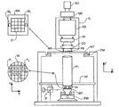
図5は、投影系と基板ステージとの間に液体貯溜部10を有する液体供給系を示す。液体貯溜部10は、入口/出口ダクト13を介して提供された水などの比較的高い屈折率を有する液体11で充填される。液体は、投影ビームの放射線が、空気または真空中よりも液体中で短い波長を有し、より小さい形体を解像できるという効果を有する。投影系の解像度限界は、特に投影ビームの波長およびシステムの開口数によって決定されることがよく知られている。液体の存在は、有効開口数を増加させるものと見なすこともできる。さらに、開口数が固定されていれば、液体は被写界深度の増大に効果的である。
FIG. 5 shows a liquid supply system having a
貯溜部10は、投影系の鏡像力場の周囲で基板に非接触シールを形成し、したがって液体は、基板表面と投影系の最終部材との間にある空間の充填に制約される。貯溜部はシール部材12によって形成され、該シール部材12は、投影系PLの最終部材を囲んでその下に配置される。液体を、投影系の下でシール部材12内の空間に入れる。シール部材12は、投影系の最終部材よりも少し上に延在しており、液体緩衝域が作られるように液体レベルが最終部材の上まで高まる。シール部材12は内周を有し、これは上端部にて投影系のステップまたはその最終部材とほぼ一致することが好ましく、例えば丸くしてよい。底部では、内周は画像領域の形状にほぼ一致し、例えば長方形であるが、そうである必要はない。
The
液体は、シール部材12の底部と基板Wの表面との間にあるガスシール16によって、貯溜部内に制約される。ガスシールはガスによって形成され、これは例えば空気または合成空気であるが、N2または別の不活性ガスであることが好ましく、入口15を通してシール部材12と基板との間の隙間に加圧状態で提供され、第一出口14を通して抽出される。ガス入口15への過剰圧力、第一出口14の真空レベル、およびギャップの幾何学的形状は、液体を制約する高速のガス流が内側にあるように構成される。あるいは、貯溜部内に液体を制約するように液体の流れが設定された液体シールを使用してよい。
The liquid is constrained in the reservoir by a
実施時には、ガスシールは2つの環状溝によって形成され、これは溝の周囲に隔置された一連の小さい導管によって、それぞれ第一入口15および第一出口14に接続される。入口15および出口14は、シール部材12の周囲を囲む複数の個別オリフィスであるか、連続的な溝またはスリットでもよい。入口および出口のそれぞれで、シール部材に大きい環状の窪みを設けて、マニホルドを形成してよい。ガスシールは、気体支承部として挙動することにより、シール部材12を支持するのにも効果的である。液体シールは、動的または静的支承部として作用してもよい。
In practice, the gas seal is formed by two annular grooves, which are connected to the
リソグラフィ装置の測定ステーションには、露光のために基板を準備したり、露光したレジストを認定したりする際に使用するために、各種センサおよび測定デバイスを設ける。その幾つかを図6に示す。基板Wは、測定ステーション(またはさらなる装填/取り出しステーション)で基板テーブルWTに装填され、必要な露光前措置を執る。例えば、レベルセンサ30は、その後、露光中に基板のレベリングに使用するために、基板全体の高さマップを作成するために使用され、アラインメントセンサ20は、基板テーブルWTに装着された透過像センサTISに組み込まれた基準マーカーに対する基板W上のアラインメントマーカーの位置を測定するために使用される。次に、露光を完了するために、基板テーブルWTおよび基板Wを露光ステーションへと移動させ、次に必要な露光後測定のために測定ステーションに戻す。スループット(処理能力)を改善するために、装置は、別の基板を測定中に、1つの基板で露光を実行できるように、装置は第二基板テーブルを有してよい。装置に基板テーブルが1つしかない場合は、露光ステーションに測定デバイスおよびセンサを設けて、レベリングなどの何らかの測定を露光と同時に実行することができる。
The measurement station of the lithographic apparatus is provided with various sensors and measurement devices for use in preparing the substrate for exposure and qualifying the exposed resist. Some of them are shown in FIG. The substrate W is loaded onto the substrate table WT at a measurement station (or further loading / unloading station) and takes necessary pre-exposure measures. For example, the
本発明の一具体例では、露光後認定プロセスは、露光が完了した後に基板および/または基板テーブル上に残った残留液体の検出を含む。液体供給系は、露光に使用した液体を可能な限り全て除去するように配置構成されているが、多少の液体が残る可能性がある。基板上の液体は、例えば露光後の焼成プロセスで温度変動を引き起こし、その後の基板処理に問題を起こすことがある。残留液体から生じる蒸気は、露光後焼成に使用する焼成プレートの腐食も引き起こす。基板テーブル上の残留液体も腐食を引き起こすか、基準マーカーの位置を測定しようとする場合に、アラインメントセンサなどのセンサの動作を妨害することがある。基板テーブルの側面上を、干渉計位置測定系のミラーへと移動するような残留液体は、そのシステムの出力にエラーを引き起こすことがある。残留液体は、図6では小滴として図示されているが、薄膜の形態をとることもある。 In one embodiment of the invention, the post-exposure qualification process includes detection of residual liquid remaining on the substrate and / or substrate table after the exposure is complete. The liquid supply system is arranged and configured to remove as much of the liquid used for exposure as possible, but some liquid may remain. The liquid on the substrate may cause temperature fluctuations in the baking process after exposure, for example, and may cause problems in subsequent substrate processing. The vapor generated from the residual liquid also causes corrosion of the baking plate used for post exposure baking. Residual liquid on the substrate table can also cause corrosion or interfere with the operation of a sensor, such as an alignment sensor, when attempting to measure the position of a fiducial marker. Residual liquid, such as moving on the side of the substrate table to the mirror of the interferometer position measurement system, can cause errors in the output of the system. The residual liquid is illustrated as a droplet in FIG. 6, but may take the form of a thin film.
基板および/または基板テーブル上の残留液体を検出する一つの方法は、レベルセンサ30で高さマッピングプロセスを実行することである。残留液体の存在は、センサの標準動作範囲以外での高さおよび/または傾斜測定値によって、または基準高さマップから、または露光前に実行した高さマップからの大きな変動によって示される。残留液体は、アラインメントセンサ20でアラインメント測定を実行することによっても検出することができる。この場合も、センサの標準動作範囲以外の測定値、または、露光前測定値からの大きな変動が、残留液体を示す。
One way to detect residual liquid on the substrate and / or substrate table is to perform a height mapping process with the
残留液体が検出された場合は、手動是正措置をとるようにオペレータに指示するために、警報信号を発出させてもよい。代替的に、一体化された自動乾燥系を起動するか、乾燥プロセスを既に実行している場合は、再起動する。基板上に残留液体が検出された場合は、基板を通常の方法でトラックユニットへと取り出すが、露光後焼成、または、液体の存在で影響を受けやすいその他のプロセスの前に、スピン乾燥等の追加の乾燥ステップを実行するようにトラックユニットに命令するために、エラーコードフラグを付随させることができる。 If residual liquid is detected, an alarm signal may be issued to instruct the operator to take manual corrective action. Alternatively, the integrated automatic drying system is started or restarted if a drying process has already been performed. If residual liquid is detected on the substrate, the substrate is removed to the track unit in the normal manner, but after exposure or after other processes that are sensitive to the presence of liquid, such as spin drying. An error code flag can be associated to instruct the truck unit to perform an additional drying step.
別の例では、専用の液体検出器を使用して、残留液体を検出する。これは、容量センサ40および/または図7で示すような空気ゲージ50の形態をとってよい。他の可能なタイプのセンサは、スキャッタセンサ、カメラ、例えばCCDカメラ、蒸発のためにさらに低温であるスポットを検出する赤外線センサ、および基板上の粒子を検出する既知のセンサを含む。自動焦点スポット投影装置も使用することができる。このようなデバイスは、CDまたは他の光学ディスクドライブのピックアップ内で往々にして見られ、平行ビームを基板上に集束するためにボイスコイルに装着されたコリメーティングレンズ(平行化レンズ)を有する。反射ビームは、カッドセル光検出器(quad cell photodetector)等の検出器に指向せしめられ、これは、例えば反射ビームの楕円率を検出することにより、基板上のスポットが焦点にあるか否かを検出する。次に、サーボ回路がコリメーティングレンズの位置を調節して、基板上のスポットを焦点に合わせる。基板上に液体が存在すると、レンズと基板の間の光路長が変化し、したがってレンズが補償のために移動する。この移動は、例えばボイスコイルへの駆動信号を監視し、液体の存在を示すことによって検出することができる。このようなデバイスは、基板上に投影されたビームのスポットが非常に小さく、例えば回折限界にでき、したがって非常に小さい液体小滴を検出できると有利である。図8を見ると、別の可能なタイプのセンサは、残留液体によって散乱した光を検出するためにレーザ放出器60および光検出器61を有する。
In another example, a dedicated liquid detector is used to detect residual liquid. This may take the form of a
基板テーブルは、検出器を越えて走査されるか、検出器をロボットアーム上に設けて、基板および/または基板テーブルを検出することができる。放出器/検出器センサの場合、放出されたビームは、例えば回転する多角形ミラーを使用して、基板を走査するように配置構成することができる。残留液体の検出にかかる時間を短縮するか、基板および基板テーブル表面の異なる部分で使用するために、複数の検出器を設けてよい。 The substrate table can be scanned beyond the detector or the detector can be provided on the robot arm to detect the substrate and / or substrate table. In the case of an emitter / detector sensor, the emitted beam can be arranged to scan the substrate, for example using a rotating polygon mirror. Multiple detectors may be provided to reduce the time it takes to detect residual liquid or to use on different parts of the substrate and substrate table surfaces.
特に装置が単一ステージ装置である場合、残留液体を検出するための1つまたは複数のセンサを露光ステーションに設けて、1回または複数回の露光と並行して(つまり、先に露光された目標位置で液体を検出する)、または、全ての露光を終えた後に、該検出センサを作動させてもよいことに留意すべきである。十分に小型であれば、1つまたは複数のセンサを液体供給系に設けてもよい。 In particular, if the apparatus is a single stage apparatus, the exposure station is provided with one or more sensors for detecting residual liquid and in parallel with one or more exposures (ie, previously exposed) It should be noted that the detection sensor may be activated after all exposure has been completed (detecting liquid at the target position). If sufficiently small, one or more sensors may be provided in the liquid supply system.
別例では、基板テーブル上の残留液体の追加重量を検出することによって残留液体の検出が行われる。これは、一定の鉛直方向位置に維持するためにZアクチュエータまたは重量補償装置によって基板テーブルに加える力を監視する回路またはソフトウェアルーチンによって実行することができる。 In another example, residual liquid detection is performed by detecting an additional weight of residual liquid on the substrate table. This can be done by a circuit or software routine that monitors the force applied to the substrate table by the Z actuator or weight compensator to maintain a constant vertical position.
代替例では、追加重量は、各計量センサが基板リフトピンを伴う計量センサ装置に、前記リフトピンによって基板テーブルから持上げられている場合に基板が平衡を失っているか判断させることによっても検出することができる。 In an alternative example, the additional weight can also be detected by having a weighing sensor device, each weighing sensor with a substrate lift pin, determine whether the substrate has lost balance when lifted from the substrate table by the lift pin. .
本発明は、任意の浸漬リソグラフィに、特に前述したタイプに適用することができるが、それに限定されない。 The present invention can be applied to any immersion lithography, particularly but not limited to the types described above.
基板または基板テーブル上の残留液体の検出以外に、本発明は同様に、基板テーブルおよび/またはセンサ上の粒子の検出にも適切である。このような粒子を検出して、それを除去させると有利である。というのは、粒子が、基板テーブルの走査運動中に浸漬流体によって拾われ、次に基板表面に落ち着くことがあり、これは目標部分に作られるデバイスの欠陥につながるからである。 Besides detecting residual liquid on the substrate or substrate table, the present invention is also suitable for detecting particles on the substrate table and / or sensor. It is advantageous to detect such particles and remove them. This is because particles may be picked up by the immersion fluid during the scanning motion of the substrate table and then settle to the substrate surface, which leads to defects in the device created in the target portion.
本文ではICの製造におけるリソグラフィ装置の使用に特に言及しているが、本明細書で説明するリソグラフィ装置がその他の多くの用途においても使用可能である。例えば、これは、集積光学装置、磁気ドメインメモリ用ガイダンスおよび検出パターン、フラットパネルディスプレイ、液晶ディスプレイ(LCD)、薄膜磁気ヘッド等の製造に使用され得る。こうした代替的な用途においては、本文にて使用した用語「ウェハ」または「ダイ」は、それぞれ「基板」または「目標部分」といった、より一般的な用語に置き換えて使用され得ることが当業者には理解される。本明細書で言及する基板は、露光前または露光後に、例えばトラック(通常はレジストの層を基板に塗布し、露光したレジストを現像するツール)または計測または検査ツールで処理することができる。適宜、本明細書の開示は、以上およびその他の基板処理ツールに適用することができる。さらに、基板は、例えば多層ICを生成するために、複数回処理することができ、したがって本明細書で用いる用語「基板」は、既に複数の処理済み層を含む基板も指す。 Although this text specifically refers to the use of lithographic apparatus in the manufacture of ICs, the lithographic apparatus described herein can be used in many other applications. For example, it can be used in the manufacture of integrated optical devices, magnetic domain memory guidance and detection patterns, flat panel displays, liquid crystal displays (LCDs), thin film magnetic heads and the like. In such alternative applications, one skilled in the art will recognize that the terms “wafer” or “die” as used herein may be used in place of more general terms such as “substrate” or “target portion”, respectively. Is understood. The substrate referred to herein can be processed before or after exposure, for example, with a track (usually a tool that applies a layer of resist to the substrate and develops the exposed resist) or a metrology or inspection tool. Where appropriate, the disclosure herein may be applied to these and other substrate processing tools. Furthermore, the substrate can be processed multiple times, for example to produce a multi-layer IC, and thus the term “substrate” as used herein also refers to a substrate that already contains multiple processed layers.
以上では、本発明の具体例での使用を光学リソグラフィの文脈で言及しているが、本発明は、例えばインプリントリソグラフィなどのその他の用途にも使用することができ、状況が許せば、光学リソグラフィに制限されない。インプリントリソグラフィでは、パターン付与デバイスのトポグラフィが基板上に作られるパターンを規定する。パターン付与デバイスのトポグラフィを、基板に供給されたレジストの層に押しつけ、その後に電磁放射線、熱、圧力またはその組み合わせを加えて、レジストを硬化する。パターン付与デバイスをレジストから外し、レジストの硬化後にパターンをそこに残す。 Although the foregoing refers to the use of embodiments of the present invention in the context of optical lithography, the present invention can also be used for other applications, such as imprint lithography, and if the situation allows, optical It is not limited to lithography. In imprint lithography, the topography of the patterning device defines the pattern that is created on the substrate. The topography of the patterning device is pressed against a layer of resist supplied to the substrate, followed by application of electromagnetic radiation, heat, pressure or a combination thereof to cure the resist. The patterning device is removed from the resist, leaving the pattern in it after the resist is cured.
本明細書では、「放射線」および「ビーム」という用語は、イオンビームあるいは電子ビームといったような粒子ビームのみならず、紫外線(UV)放射線(例えば、365nm、248nm、193nm、157nm、あるいは126nmの波長を有する)および超紫外線(EUV)放射線(例えば、5nm〜20nmの範囲の波長を有する)を含むあらゆる種類の電磁放射線を網羅するものとして使用される。 As used herein, the terms “radiation” and “beam” include not only particle beams such as ion beams or electron beams, but also ultraviolet (UV) radiation (eg, wavelengths of 365 nm, 248 nm, 193 nm, 157 nm, or 126 nm). And extreme ultraviolet (EUV) radiation (eg having a wavelength in the range of 5 nm to 20 nm) is used to cover all types of electromagnetic radiation.
「レンズ」という用語は、状況が許せば様々な光学構成要素のうち任意の1つまたはその組み合わせを指す。例えば屈折、反射、磁気、電磁気および静電光学構成要素である。 The term “lens” refers to any one or combination of various optical components where circumstances permit. For example, refractive, reflective, magnetic, electromagnetic and electrostatic optical components.
以上、本発明の実施形態を詳細に説明したが、説明とは異なる方法でも本発明を実践できることが理解される。例えば、本発明の実施形態は、上記で開示したような方法を記述する機械で読み取り可能な命令の1つまたは複数のシーケンスを有するコンピュータプログラム、またはこのようなコンピュータプログラムが記憶されたデータ記憶媒体(例えば、半導体メモリ、磁気または光ディスク)の形態をとることができる。 As mentioned above, although embodiment of this invention was described in detail, it understands that this invention can be practiced by the method different from description. For example, an embodiment of the present invention is a computer program having one or more sequences of machine readable instructions describing a method as disclosed above, or a data storage medium having such a computer program stored on it. (Eg, semiconductor memory, magnetic or optical disk).
以上の説明は例示目的であり、限定的なものではない。したがって、特許請求の範囲から逸脱することなく、前記本発明を変形できることが当業者には明白である。 The above description is illustrative and not restrictive. Thus, it will be apparent to one skilled in the art that modifications may be made to the invention without departing from the scope of the claims set out below.
Claims (13)
前記投影系と前記基板との間の空間に液体を供給する液体供給系と、
投影完了後に、前記基板および/または前記基板を保持するテーブルに残った残留液体を検出する残留液体検出器と、を有し、
前記残留液体検出器は、空気ゲージ、自動焦点スポット投影装置、スキャッタロメータ、赤外線センサ、並びに、グレージング角レーザビーム及び散乱光を検出するための検出器、を含む群から選択された1つまたは複数のデバイスと、とを含み、
パターン付与されたビームが投影された先の目標箇所での前記残留液体の検出が、パターン付与されたビームの投影と並行して実行される、リソグラフィ投影装置。 A projection system for projecting the patterned radiation beam onto the substrate;
A liquid supply system for supplying a liquid to a space between the projection system and the substrate;
A residual liquid detector for detecting residual liquid remaining on the substrate and / or a table holding the substrate after projection is completed;
The residual liquid detector is one selected from the group comprising an air gauge, an autofocus spot projector, a scatterometer, an infrared sensor, and a detector for detecting a glazing angle laser beam and scattered light, or and a plurality of devices, the city only including,
A lithographic projection apparatus , wherein the detection of the residual liquid at a target location onto which a patterned beam has been projected is performed in parallel with the projection of the patterned beam .
リソグラフィ装置の投影系を用いる段階と、
パターン付与された放射線ビームを、液体を通して基板に投影する段階と、
投影完了後に、前記基板および/または前記基板を保持するテーブルの表面の残留液体を検出する段階とを含み、
前記残留液体検出器は、空気ゲージ、自動焦点スポット投影装置、スキャッタロメータ、赤外線センサ、並びに、グレージング角レーザビーム及び散乱光を検出するための検出器、を含む群から選択された1つまたは複数のデバイスと、とを含み、
パターン付与されたビームが投影された先の目標箇所での前記残留液体を検出する段階が、パターン付与されたビームの投影と並行して実行される、デバイス製造方法。 A projection stage;
Using a projection system of a lithographic apparatus;
Projecting a patterned beam of radiation through a liquid onto a substrate;
Detecting residual liquid on the surface of the substrate and / or the table holding the substrate after projection is completed,
The residual liquid detector is one selected from the group comprising an air gauge, an autofocus spot projector, a scatterometer, an infrared sensor, and a detector for detecting a glazing angle laser beam and scattered light, or and a plurality of devices, the city only including,
A method of manufacturing a device , wherein the step of detecting the residual liquid at a target location onto which a patterned beam has been projected is performed in parallel with the projection of the patterned beam .
Applications Claiming Priority (2)
| Application Number | Priority Date | Filing Date | Title |
|---|---|---|---|
| US10/885489 | 2004-07-07 | ||
| US10/885,489 US7463330B2 (en) | 2004-07-07 | 2004-07-07 | Lithographic apparatus and device manufacturing method |
Related Parent Applications (1)
| Application Number | Title | Priority Date | Filing Date |
|---|---|---|---|
| JP2009000117A Division JP4898848B2 (en) | 2004-07-07 | 2009-01-05 | Lithographic apparatus and device manufacturing method |
Publications (2)
| Publication Number | Publication Date |
|---|---|
| JP2010183099A JP2010183099A (en) | 2010-08-19 |
| JP4970566B2 true JP4970566B2 (en) | 2012-07-11 |
Family
ID=35540974
Family Applications (3)
| Application Number | Title | Priority Date | Filing Date |
|---|---|---|---|
| JP2005197421A Expired - Fee Related JP4342482B2 (en) | 2004-07-07 | 2005-07-06 | Lithographic apparatus and device manufacturing method |
| JP2009000117A Expired - Fee Related JP4898848B2 (en) | 2004-07-07 | 2009-01-05 | Lithographic apparatus and device manufacturing method |
| JP2010088441A Active JP4970566B2 (en) | 2004-07-07 | 2010-04-07 | Lithographic projection apparatus and device manufacturing method |
Family Applications Before (2)
| Application Number | Title | Priority Date | Filing Date |
|---|---|---|---|
| JP2005197421A Expired - Fee Related JP4342482B2 (en) | 2004-07-07 | 2005-07-06 | Lithographic apparatus and device manufacturing method |
| JP2009000117A Expired - Fee Related JP4898848B2 (en) | 2004-07-07 | 2009-01-05 | Lithographic apparatus and device manufacturing method |
Country Status (2)
| Country | Link |
|---|---|
| US (5) | US7463330B2 (en) |
| JP (3) | JP4342482B2 (en) |
Families Citing this family (50)
| Publication number | Priority date | Publication date | Assignee | Title |
|---|---|---|---|---|
| EP2166413A1 (en) | 2003-04-11 | 2010-03-24 | Nikon Corporation | Cleanup method for optics in immersion lithography |
| SG2012031217A (en) * | 2003-04-11 | 2015-09-29 | Nippon Kogaku Kk | Apparatus having an immersion fluid system configured to maintain immersion fluid in a gap adjacent an optical assembly |
| TWI518742B (en) | 2003-05-23 | 2016-01-21 | 尼康股份有限公司 | A method of manufacturing an exposure apparatus and an element |
| ATE453209T1 (en) | 2003-06-19 | 2010-01-15 | Nikon Corp | EXPOSURE DEVICE AND COMPONENT PRODUCTION METHOD |
| SG109000A1 (en) | 2003-07-16 | 2005-02-28 | Asml Netherlands Bv | Lithographic apparatus and device manufacturing method |
| KR101599649B1 (en) | 2003-07-28 | 2016-03-14 | 가부시키가이샤 니콘 | Exposure apparatus, device producing method, and exposure apparatus controlling method |
| TWI245163B (en) | 2003-08-29 | 2005-12-11 | Asml Netherlands Bv | Lithographic apparatus and device manufacturing method |
| EP3093711A3 (en) | 2003-09-29 | 2017-05-24 | Nikon Corporation | Exposure apparatus, exposure method, and method for producing device |
| EP1672681B8 (en) * | 2003-10-08 | 2011-09-21 | Miyagi Nikon Precision Co., Ltd. | Exposure apparatus, substrate carrying method, exposure method, and method for producing device |
| JP2005136364A (en) * | 2003-10-08 | 2005-05-26 | Zao Nikon Co Ltd | Substrate carrying device, exposure device and device manufacturing method |
| US7589822B2 (en) * | 2004-02-02 | 2009-09-15 | Nikon Corporation | Stage drive method and stage unit, exposure apparatus, and device manufacturing method |
| JP4506674B2 (en) | 2004-02-03 | 2010-07-21 | 株式会社ニコン | Exposure apparatus and device manufacturing method |
| US7616383B2 (en) | 2004-05-18 | 2009-11-10 | Asml Netherlands B.V. | Lithographic apparatus and device manufacturing method |
| CN101095213B (en) | 2004-06-09 | 2010-05-05 | 尼康股份有限公司 | Exposure apparatus and device manufacturing method |
| US7463330B2 (en) | 2004-07-07 | 2008-12-09 | Asml Netherlands B.V. | Lithographic apparatus and device manufacturing method |
| KR101433491B1 (en) * | 2004-07-12 | 2014-08-22 | 가부시키가이샤 니콘 | Exposure equipment and device manufacturing method |
| KR101331631B1 (en) * | 2004-10-15 | 2013-11-20 | 가부시키가이샤 니콘 | Exposure apparatus and device manufacturing method |
| US7414699B2 (en) * | 2004-11-12 | 2008-08-19 | Asml Netherlands B.V. | Lithographic apparatus and device manufacturing method |
| US20070002296A1 (en) * | 2005-06-30 | 2007-01-04 | Taiwan Semiconductor Manufacturing Company, Ltd. | Immersion lithography defect reduction |
| US7927779B2 (en) * | 2005-06-30 | 2011-04-19 | Taiwan Semiconductor Manufacturing Companym, Ltd. | Water mark defect prevention for immersion lithography |
| TW200710616A (en) * | 2005-07-11 | 2007-03-16 | Nikon Corp | Exposure apparatus and method for manufacturing device |
| US8383322B2 (en) * | 2005-08-05 | 2013-02-26 | Taiwan Semiconductor Manufacturing Company, Ltd. | Immersion lithography watermark reduction |
| US7993808B2 (en) | 2005-09-30 | 2011-08-09 | Taiwan Semiconductor Manufacturing Company, Ltd. | TARC material for immersion watermark reduction |
| JP2007103658A (en) * | 2005-10-04 | 2007-04-19 | Canon Inc | Method and device for exposure as well as method of manufacturing device |
| US7929109B2 (en) * | 2005-10-20 | 2011-04-19 | Nikon Corporation | Apparatus and method for recovering liquid droplets in immersion lithography |
| JP4889331B2 (en) * | 2006-03-22 | 2012-03-07 | 大日本スクリーン製造株式会社 | Substrate processing apparatus and substrate processing method |
| WO2007135990A1 (en) * | 2006-05-18 | 2007-11-29 | Nikon Corporation | Exposure method and apparatus, maintenance method and device manufacturing method |
| CN102109773A (en) * | 2006-05-22 | 2011-06-29 | 株式会社尼康 | Exposure method, exposure apparatus, and maintenance method |
| JP2007335476A (en) * | 2006-06-12 | 2007-12-27 | Canon Inc | Exposure apparatus and device manufacturing method |
| JP5151981B2 (en) * | 2006-08-30 | 2013-02-27 | 株式会社ニコン | Exposure apparatus and device manufacturing method |
| JP2008066341A (en) * | 2006-09-04 | 2008-03-21 | Canon Inc | Carrying device, and exposure device and method |
| US8518628B2 (en) * | 2006-09-22 | 2013-08-27 | Taiwan Semiconductor Manufacturing Company, Ltd. | Surface switchable photoresist |
| US7986146B2 (en) * | 2006-11-29 | 2011-07-26 | Globalfoundries Inc. | Method and system for detecting existence of an undesirable particle during semiconductor fabrication |
| US9632425B2 (en) | 2006-12-07 | 2017-04-25 | Asml Holding N.V. | Lithographic apparatus, a dryer and a method of removing liquid from a surface |
| JP5169492B2 (en) * | 2007-05-30 | 2013-03-27 | 株式会社ニコン | Exposure apparatus, exposure method, and device manufacturing method |
| US8098362B2 (en) * | 2007-05-30 | 2012-01-17 | Nikon Corporation | Detection device, movable body apparatus, pattern formation apparatus and pattern formation method, exposure apparatus and exposure method, and device manufacturing method |
| SG151198A1 (en) * | 2007-09-27 | 2009-04-30 | Asml Netherlands Bv | Methods relating to immersion lithography and an immersion lithographic apparatus |
| US8786829B2 (en) * | 2008-05-13 | 2014-07-22 | Nikon Corporation | Exposure apparatus, exposure method, and device manufacturing method |
| US8228482B2 (en) * | 2008-05-13 | 2012-07-24 | Nikon Corporation | Exposure apparatus, exposure method, and device manufacturing method |
| US8817236B2 (en) * | 2008-05-13 | 2014-08-26 | Nikon Corporation | Movable body system, movable body drive method, pattern formation apparatus, pattern formation method, exposure apparatus, exposure method, and device manufacturing method |
| NL2002998A1 (en) * | 2008-06-18 | 2009-12-22 | Asml Netherlands Bv | Lithographic apparatus. |
| JP5199982B2 (en) * | 2008-12-08 | 2013-05-15 | エーエスエムエル ネザーランズ ビー.ブイ. | Lithographic apparatus |
| US8941809B2 (en) * | 2008-12-22 | 2015-01-27 | Screen Semiconductor Solutions Co., Ltd. | Substrate processing apparatus and substrate processing method |
| JP5371413B2 (en) * | 2008-12-22 | 2013-12-18 | 株式会社Sokudo | Substrate processing apparatus and substrate processing method |
| NL2005528A (en) * | 2009-12-02 | 2011-06-07 | Asml Netherlands Bv | Lithographic apparatus and device manufacturing method. |
| NL2009612A (en) * | 2011-11-21 | 2013-05-23 | Asml Netherlands Bv | Level sensor, a method for determining a height map of a substrate, and a lithographic apparatus. |
| WO2013160082A1 (en) | 2012-04-27 | 2013-10-31 | Asml Netherlands B.V. | Lithographic apparatus |
| JP6419581B2 (en) * | 2015-01-08 | 2018-11-07 | 株式会社東芝 | Semiconductor device manufacturing apparatus and semiconductor device manufacturing apparatus management method |
| NL2020556A (en) | 2017-04-20 | 2018-10-24 | Asml Netherlands Bv | A Method of Performance Testing Working Parameters of a Fluid Handling Structure and A Method of Detecting Loss of Immersion Liquid from a Fluid Handing Structure in an Immersion Lithographic Apparatus |
| CN113189849B (en) | 2021-04-22 | 2023-08-11 | 中国科学院光电技术研究所 | A near-field lithography immersion system and its immersion unit and interface module |
Family Cites Families (255)
| Publication number | Priority date | Publication date | Assignee | Title |
|---|---|---|---|---|
| DE224448C (en) | ||||
| DE206607C (en) | ||||
| DE242880C (en) | ||||
| DE221563C (en) | ||||
| GB1242527A (en) | 1967-10-20 | 1971-08-11 | Kodak Ltd | Optical instruments |
| US3573975A (en) | 1968-07-10 | 1971-04-06 | Ibm | Photochemical fabrication process |
| JPS5919912Y2 (en) | 1978-08-21 | 1984-06-08 | 清水建設株式会社 | composite heat exchanger |
| ATE1462T1 (en) | 1979-07-27 | 1982-08-15 | Werner W. Dr. Tabarelli | OPTICAL LITHOGRAPHY PROCESS AND DEVICE FOR COPYING A PATTERN ONTO A SEMICONDUCTOR DISC. |
| FR2474708B1 (en) | 1980-01-24 | 1987-02-20 | Dme | HIGH-RESOLUTION MICROPHOTOLITHOGRAPHY PROCESS |
| JPS5754317A (en) | 1980-09-19 | 1982-03-31 | Hitachi Ltd | Method and device for forming pattern |
| US4346164A (en) | 1980-10-06 | 1982-08-24 | Werner Tabarelli | Photolithographic method for the manufacture of integrated circuits |
| US4509852A (en) | 1980-10-06 | 1985-04-09 | Werner Tabarelli | Apparatus for the photolithographic manufacture of integrated circuit elements |
| JPS57117238A (en) | 1981-01-14 | 1982-07-21 | Nippon Kogaku Kk <Nikon> | Exposing and baking device for manufacturing integrated circuit with illuminometer |
| JPS6113794Y2 (en) | 1981-01-16 | 1986-04-28 | ||
| US4390273A (en) | 1981-02-17 | 1983-06-28 | Censor Patent-Und Versuchsanstalt | Projection mask as well as a method and apparatus for the embedding thereof and projection printing system |
| JPS57153433A (en) | 1981-03-18 | 1982-09-22 | Hitachi Ltd | Manufacturing device for semiconductor |
| JPS57153433U (en) | 1981-03-20 | 1982-09-27 | ||
| JPS58202448A (en) | 1982-05-21 | 1983-11-25 | Hitachi Ltd | Exposing device |
| DD206607A1 (en) | 1982-06-16 | 1984-02-01 | Mikroelektronik Zt Forsch Tech | METHOD AND DEVICE FOR ELIMINATING INTERFERENCE EFFECTS |
| JPS5919912A (en) | 1982-07-26 | 1984-02-01 | Hitachi Ltd | Immersion distance holding device |
| DD242880A1 (en) | 1983-01-31 | 1987-02-11 | Kuch Karl Heinz | DEVICE FOR PHOTOLITHOGRAPHIC STRUCTURAL TRANSMISSION |
| DD221563A1 (en) | 1983-09-14 | 1985-04-24 | Mikroelektronik Zt Forsch Tech | IMMERSIONS OBJECTIVE FOR THE STEP-BY-STEP PROJECTION IMAGING OF A MASK STRUCTURE |
| DD224448A1 (en) | 1984-03-01 | 1985-07-03 | Zeiss Jena Veb Carl | DEVICE FOR PHOTOLITHOGRAPHIC STRUCTURAL TRANSMISSION |
| JPS60229606A (en) | 1984-04-27 | 1985-11-15 | 株式会社日立製作所 | Gas insulated switching device |
| JPS61113376A (en) | 1984-11-07 | 1986-05-31 | Sony Corp | Television signal movement detector |
| JPH0653120B2 (en) | 1985-05-10 | 1994-07-20 | オリンパス光学工業株式会社 | Ultrasonic diagnostic equipment |
| JPS6265326A (en) | 1985-09-18 | 1987-03-24 | Hitachi Ltd | Exposure device |
| JPS6265326U (en) | 1985-10-16 | 1987-04-23 | ||
| JPS62121417A (en) | 1985-11-22 | 1987-06-02 | Hitachi Ltd | Liquid-immersion objective lens device |
| JPS62121417U (en) | 1986-01-24 | 1987-08-01 | ||
| JPH0695511B2 (en) * | 1986-09-17 | 1994-11-24 | 大日本スクリ−ン製造株式会社 | Washing and drying treatment method |
| JPS6373628U (en) | 1986-10-31 | 1988-05-17 | ||
| JPS63157419A (en) | 1986-12-22 | 1988-06-30 | Toshiba Corp | Fine pattern transfer apparatus |
| JPS63157419U (en) | 1987-03-31 | 1988-10-14 | ||
| US5040020A (en) | 1988-03-31 | 1991-08-13 | Cornell Research Foundation, Inc. | Self-aligned, high resolution resonant dielectric lithography |
| JPH0766114B2 (en) | 1988-11-11 | 1995-07-19 | 富士電気化学株式会社 | Magneto-optical element material |
| JPH03209479A (en) | 1989-09-06 | 1991-09-12 | Sanee Giken Kk | Exposure method |
| JP2897355B2 (en) | 1990-07-05 | 1999-05-31 | 株式会社ニコン | Alignment method, exposure apparatus, and position detection method and apparatus |
| JPH04305915A (en) | 1991-04-02 | 1992-10-28 | Nikon Corp | Adhesion type exposure device |
| JPH04305917A (en) | 1991-04-02 | 1992-10-28 | Nikon Corp | Adhesion type exposure device |
| US5240020A (en) * | 1991-05-28 | 1993-08-31 | Byers Wayne L | Retractable fisherman's shade and method for operating |
| JPH0562877A (en) | 1991-09-02 | 1993-03-12 | Yasuko Shinohara | Optical system for lsi manufacturing contraction projection aligner by light |
| JP3246615B2 (en) | 1992-07-27 | 2002-01-15 | 株式会社ニコン | Illumination optical device, exposure apparatus, and exposure method |
| JPH06188169A (en) | 1992-08-24 | 1994-07-08 | Canon Inc | Method of image formation, exposure system, and manufacture of device |
| JP3395797B2 (en) * | 1993-08-31 | 2003-04-14 | 株式会社ニコン | Exposure equipment |
| JPH06124873A (en) * | 1992-10-09 | 1994-05-06 | Canon Inc | Liquid-soaking type projection exposure apparatus |
| JP2753930B2 (en) | 1992-11-27 | 1998-05-20 | キヤノン株式会社 | Immersion type projection exposure equipment |
| JP2520833B2 (en) | 1992-12-21 | 1996-07-31 | 東京エレクトロン株式会社 | Immersion type liquid treatment device |
| JP3412704B2 (en) | 1993-02-26 | 2003-06-03 | 株式会社ニコン | Projection exposure method and apparatus, and exposure apparatus |
| JPH07220990A (en) | 1994-01-28 | 1995-08-18 | Hitachi Ltd | Pattern forming method and exposure apparatus therefor |
| US5528118A (en) | 1994-04-01 | 1996-06-18 | Nikon Precision, Inc. | Guideless stage with isolated reaction stage |
| US5874820A (en) | 1995-04-04 | 1999-02-23 | Nikon Corporation | Window frame-guided stage mechanism |
| JP3555230B2 (en) | 1994-05-18 | 2004-08-18 | 株式会社ニコン | Projection exposure equipment |
| US5623853A (en) | 1994-10-19 | 1997-04-29 | Nikon Precision Inc. | Precision motion stage with single guide beam and follower stage |
| JP3195200B2 (en) * | 1994-12-09 | 2001-08-06 | キヤノン株式会社 | Semiconductor exposure apparatus and foreign matter detection method |
| JPH08316125A (en) | 1995-05-19 | 1996-11-29 | Hitachi Ltd | Method and apparatus for projection exposing |
| JPH08316124A (en) | 1995-05-19 | 1996-11-29 | Hitachi Ltd | Method and apparatus for projection exposing |
| EP0829036B9 (en) * | 1996-04-01 | 2001-07-25 | ASM Lithography B.V. | Lithographic scanning exposure projection apparatus |
| US6012966A (en) * | 1996-05-10 | 2000-01-11 | Canon Kabushiki Kaisha | Precision polishing apparatus with detecting means |
| WO1998009278A1 (en) | 1996-08-26 | 1998-03-05 | Digital Papyrus Technologies | Method and apparatus for coupling an optical lens to a disk through a coupling medium having a relatively high index of refraction |
| US5825043A (en) | 1996-10-07 | 1998-10-20 | Nikon Precision Inc. | Focusing and tilting adjustment system for lithography aligner, manufacturing apparatus or inspection apparatus |
| SG102627A1 (en) | 1996-11-28 | 2004-03-26 | Nikon Corp | Lithographic device |
| JP4029182B2 (en) | 1996-11-28 | 2008-01-09 | 株式会社ニコン | Exposure method |
| JP4029183B2 (en) | 1996-11-28 | 2008-01-09 | 株式会社ニコン | Projection exposure apparatus and projection exposure method |
| DE69717975T2 (en) | 1996-12-24 | 2003-05-28 | Asml Netherlands B.V., Veldhoven | POSITIONER BALANCED IN TWO DIRECTIONS, AND LITHOGRAPHIC DEVICE WITH SUCH A POSITIONER |
| JP3612920B2 (en) | 1997-02-14 | 2005-01-26 | ソニー株式会社 | Exposure apparatus for producing an optical recording medium master |
| JPH10255319A (en) | 1997-03-12 | 1998-09-25 | Hitachi Maxell Ltd | Master disk exposure device and method therefor |
| JP3747566B2 (en) | 1997-04-23 | 2006-02-22 | 株式会社ニコン | Immersion exposure equipment |
| JP3817836B2 (en) | 1997-06-10 | 2006-09-06 | 株式会社ニコン | EXPOSURE APPARATUS, ITS MANUFACTURING METHOD, EXPOSURE METHOD, AND DEVICE MANUFACTURING METHOD |
| JPH1116816A (en) | 1997-06-25 | 1999-01-22 | Nikon Corp | Projection aligner, method for exposure with the device, and method for manufacturing circuit device using the device |
| US5900354A (en) | 1997-07-03 | 1999-05-04 | Batchelder; John Samuel | Method for optical inspection and lithography |
| JP4210871B2 (en) | 1997-10-31 | 2009-01-21 | 株式会社ニコン | Exposure equipment |
| JPH11176727A (en) | 1997-12-11 | 1999-07-02 | Nikon Corp | Projection aligner |
| AU1505699A (en) | 1997-12-12 | 1999-07-05 | Nikon Corporation | Projection exposure method and projection aligner |
| US6208407B1 (en) | 1997-12-22 | 2001-03-27 | Asm Lithography B.V. | Method and apparatus for repetitively projecting a mask pattern on a substrate, using a time-saving height measurement |
| WO1999049504A1 (en) | 1998-03-26 | 1999-09-30 | Nikon Corporation | Projection exposure method and system |
| JP2000058436A (en) | 1998-08-11 | 2000-02-25 | Nikon Corp | Projection aligner and exposure method |
| TWI242111B (en) | 1999-04-19 | 2005-10-21 | Asml Netherlands Bv | Gas bearings for use in vacuum chambers and their application in lithographic projection apparatus |
| JP4504479B2 (en) | 1999-09-21 | 2010-07-14 | オリンパス株式会社 | Immersion objective lens for microscope |
| JP2001118773A (en) * | 1999-10-18 | 2001-04-27 | Nikon Corp | Stage device and exposure system |
| US7187503B2 (en) * | 1999-12-29 | 2007-03-06 | Carl Zeiss Smt Ag | Refractive projection objective for immersion lithography |
| US6995930B2 (en) | 1999-12-29 | 2006-02-07 | Carl Zeiss Smt Ag | Catadioptric projection objective with geometric beam splitting |
| JP2001272604A (en) | 2000-03-27 | 2001-10-05 | Olympus Optical Co Ltd | Immersion objective lens and optical device using the same |
| JP2002014005A (en) | 2000-04-25 | 2002-01-18 | Nikon Corp | Measuring method of spatial image, measuring method of imaging characteristic, measuring device for spatial image, and exposuring device |
| TW591653B (en) | 2000-08-08 | 2004-06-11 | Koninkl Philips Electronics Nv | Method of manufacturing an optically scannable information carrier |
| KR100866818B1 (en) | 2000-12-11 | 2008-11-04 | 가부시키가이샤 니콘 | Projection optical system and exposure apparatus comprising the same |
| US20020163629A1 (en) | 2001-05-07 | 2002-11-07 | Michael Switkes | Methods and apparatus employing an index matching medium |
| KR100452317B1 (en) | 2001-07-11 | 2004-10-12 | 삼성전자주식회사 | photo-lithography fabrication system and method there of |
| US6600547B2 (en) | 2001-09-24 | 2003-07-29 | Nikon Corporation | Sliding seal |
| KR20050044371A (en) | 2001-11-07 | 2005-05-12 | 어플라이드 머티어리얼스, 인코포레이티드 | Optical spot grid array printer |
| JP2003234265A (en) | 2002-02-06 | 2003-08-22 | Canon Inc | Exposure device |
| US7092069B2 (en) | 2002-03-08 | 2006-08-15 | Carl Zeiss Smt Ag | Projection exposure method and projection exposure system |
| DE10210899A1 (en) | 2002-03-08 | 2003-09-18 | Zeiss Carl Smt Ag | Refractive projection lens for immersion lithography |
| DE10229818A1 (en) | 2002-06-28 | 2004-01-15 | Carl Zeiss Smt Ag | Focus detection method and imaging system with focus detection system |
| JP4117530B2 (en) | 2002-04-04 | 2008-07-16 | セイコーエプソン株式会社 | Liquid amount determination apparatus, exposure apparatus, and liquid amount determination method |
| WO2003095706A2 (en) | 2002-05-07 | 2003-11-20 | Memgen Corporation | Electrochemically fabricated hermetically sealed microstructures |
| TWI242691B (en) | 2002-08-23 | 2005-11-01 | Nikon Corp | Projection optical system and method for photolithography and exposure apparatus and method using same |
| US6954993B1 (en) * | 2002-09-30 | 2005-10-18 | Lam Research Corporation | Concentric proximity processing head |
| US7367345B1 (en) | 2002-09-30 | 2008-05-06 | Lam Research Corporation | Apparatus and method for providing a confined liquid for immersion lithography |
| US6988326B2 (en) * | 2002-09-30 | 2006-01-24 | Lam Research Corporation | Phobic barrier meniscus separation and containment |
| US7383843B2 (en) | 2002-09-30 | 2008-06-10 | Lam Research Corporation | Method and apparatus for processing wafer surfaces using thin, high velocity fluid layer |
| US7093375B2 (en) * | 2002-09-30 | 2006-08-22 | Lam Research Corporation | Apparatus and method for utilizing a meniscus in substrate processing |
| JP4189196B2 (en) | 2002-10-08 | 2008-12-03 | 芝浦メカトロニクス株式会社 | Spin processing equipment |
| US6788477B2 (en) | 2002-10-22 | 2004-09-07 | Taiwan Semiconductor Manufacturing Co., Ltd. | Apparatus for method for immersion lithography |
| DE60335595D1 (en) | 2002-11-12 | 2011-02-17 | Asml Netherlands Bv | Immersion lithographic apparatus and method of making a device |
| CN101382738B (en) | 2002-11-12 | 2011-01-12 | Asml荷兰有限公司 | Lithographic projection apparatus |
| SG121822A1 (en) | 2002-11-12 | 2006-05-26 | Asml Netherlands Bv | Lithographic apparatus and device manufacturing method |
| CN100470367C (en) | 2002-11-12 | 2009-03-18 | Asml荷兰有限公司 | Lithographic apparatus and device manufacturing method |
| US7110081B2 (en) | 2002-11-12 | 2006-09-19 | Asml Netherlands B.V. | Lithographic apparatus and device manufacturing method |
| CN100568101C (en) | 2002-11-12 | 2009-12-09 | Asml荷兰有限公司 | Lithographic equipment and device making method |
| DE10253679A1 (en) | 2002-11-18 | 2004-06-03 | Infineon Technologies Ag | Optical arrangement used in the production of semiconductor components comprises a lens system arranged behind a mask, and a medium having a specified refractive index lying between the mask and the lens system |
| SG131766A1 (en) | 2002-11-18 | 2007-05-28 | Asml Netherlands Bv | Lithographic apparatus and device manufacturing method |
| DE60319658T2 (en) | 2002-11-29 | 2009-04-02 | Asml Netherlands B.V. | Lithographic apparatus and method of making a device |
| JP4423559B2 (en) | 2002-12-03 | 2010-03-03 | 株式会社ニコン | Pollutant removal method |
| DE10258718A1 (en) | 2002-12-09 | 2004-06-24 | Carl Zeiss Smt Ag | Projection lens, in particular for microlithography, and method for tuning a projection lens |
| WO2004053959A1 (en) | 2002-12-10 | 2004-06-24 | Nikon Corporation | Optical device and projection exposure apparatus using such optical device |
| US6992750B2 (en) | 2002-12-10 | 2006-01-31 | Canon Kabushiki Kaisha | Exposure apparatus and method |
| WO2004053950A1 (en) | 2002-12-10 | 2004-06-24 | Nikon Corporation | Exposure apparatus and method for manufacturing device |
| JP4352874B2 (en) | 2002-12-10 | 2009-10-28 | 株式会社ニコン | Exposure apparatus and device manufacturing method |
| KR20120127755A (en) | 2002-12-10 | 2012-11-23 | 가부시키가이샤 니콘 | Exposure apparatus and method for manufacturing device |
| WO2004053955A1 (en) | 2002-12-10 | 2004-06-24 | Nikon Corporation | Exposure system and device producing method |
| AU2003302831A1 (en) | 2002-12-10 | 2004-06-30 | Nikon Corporation | Exposure method, exposure apparatus and method for manufacturing device |
| DE10257766A1 (en) | 2002-12-10 | 2004-07-15 | Carl Zeiss Smt Ag | Method for setting a desired optical property of a projection lens and microlithographic projection exposure system |
| CN100429748C (en) | 2002-12-10 | 2008-10-29 | 株式会社尼康 | Exposure apparatus and method for producing device |
| JP4232449B2 (en) | 2002-12-10 | 2009-03-04 | 株式会社ニコン | Exposure method, exposure apparatus, and device manufacturing method |
| WO2004053952A1 (en) | 2002-12-10 | 2004-06-24 | Nikon Corporation | Exposure apparatus and method for manufacturing device |
| WO2004053957A1 (en) | 2002-12-10 | 2004-06-24 | Nikon Corporation | Surface position detection apparatus, exposure method, and device porducing method |
| KR101036114B1 (en) | 2002-12-10 | 2011-05-23 | 가부시키가이샤 니콘 | Exposure apparatus, exposure method, device manufacturing method |
| CN100370533C (en) | 2002-12-13 | 2008-02-20 | 皇家飞利浦电子股份有限公司 | Liquid removal in a method and device for irradiating spots on a layer |
| US7514699B2 (en) | 2002-12-19 | 2009-04-07 | Koninklijke Philips Electronics N.V. | Method and device for irradiating spots on a layer |
| EP1732075A3 (en) | 2002-12-19 | 2007-02-21 | Koninklijke Philips Electronics N.V. | Method and device for irradiating spots on a layer |
| US7010958B2 (en) | 2002-12-19 | 2006-03-14 | Asml Holding N.V. | High-resolution gas gauge proximity sensor |
| US6781670B2 (en) | 2002-12-30 | 2004-08-24 | Intel Corporation | Immersion lithography |
| US7090964B2 (en) | 2003-02-21 | 2006-08-15 | Asml Holding N.V. | Lithographic printing with polarized light |
| US7206059B2 (en) | 2003-02-27 | 2007-04-17 | Asml Netherlands B.V. | Stationary and dynamic radial transverse electric polarizer for high numerical aperture systems |
| US6943941B2 (en) | 2003-02-27 | 2005-09-13 | Asml Netherlands B.V. | Stationary and dynamic radial transverse electric polarizer for high numerical aperture systems |
| US7029832B2 (en) | 2003-03-11 | 2006-04-18 | Samsung Electronics Co., Ltd. | Immersion lithography methods using carbon dioxide |
| US20050164522A1 (en) | 2003-03-24 | 2005-07-28 | Kunz Roderick R. | Optical fluids, and systems and methods of making and using the same |
| KR20110104084A (en) | 2003-04-09 | 2011-09-21 | 가부시키가이샤 니콘 | Immersion Lithography Fluid Control System |
| KR101121655B1 (en) | 2003-04-10 | 2012-03-09 | 가부시키가이샤 니콘 | Environmental system including vaccum scavange for an immersion lithography apparatus |
| WO2004093160A2 (en) | 2003-04-10 | 2004-10-28 | Nikon Corporation | Run-off path to collect liquid for an immersion lithography apparatus |
| KR101745223B1 (en) | 2003-04-10 | 2017-06-08 | 가부시키가이샤 니콘 | Environmental system including a transport region for an immersion lithography apparatus |
| JP4656057B2 (en) | 2003-04-10 | 2011-03-23 | 株式会社ニコン | Electro-osmotic element for immersion lithography equipment |
| SG2012031217A (en) | 2003-04-11 | 2015-09-29 | Nippon Kogaku Kk | Apparatus having an immersion fluid system configured to maintain immersion fluid in a gap adjacent an optical assembly |
| JP4582089B2 (en) | 2003-04-11 | 2010-11-17 | 株式会社ニコン | Liquid jet recovery system for immersion lithography |
| EP2166413A1 (en) | 2003-04-11 | 2010-03-24 | Nikon Corporation | Cleanup method for optics in immersion lithography |
| EP1614000B1 (en) | 2003-04-17 | 2012-01-18 | Nikon Corporation | Immersion lithographic apparatus |
| JP4025683B2 (en) | 2003-05-09 | 2007-12-26 | 松下電器産業株式会社 | Pattern forming method and exposure apparatus |
| JP4146755B2 (en) | 2003-05-09 | 2008-09-10 | 松下電器産業株式会社 | Pattern formation method |
| TWI295414B (en) | 2003-05-13 | 2008-04-01 | Asml Netherlands Bv | Lithographic apparatus and device manufacturing method |
| EP1480065A3 (en) | 2003-05-23 | 2006-05-10 | Canon Kabushiki Kaisha | Projection optical system, exposure apparatus, and device manufacturing method |
| TWI518742B (en) | 2003-05-23 | 2016-01-21 | 尼康股份有限公司 | A method of manufacturing an exposure apparatus and an element |
| TW201515064A (en) | 2003-05-23 | 2015-04-16 | 尼康股份有限公司 | Exposure device, exposure method, and device manufacturing method |
| JP4770129B2 (en) | 2003-05-23 | 2011-09-14 | 株式会社ニコン | Exposure apparatus and device manufacturing method |
| TWI442694B (en) | 2003-05-30 | 2014-06-21 | Asml Netherlands Bv | Lithographic apparatus and device manufacturing method |
| US7213963B2 (en) | 2003-06-09 | 2007-05-08 | Asml Netherlands B.V. | Lithographic apparatus and device manufacturing method |
| EP1486827B1 (en) | 2003-06-11 | 2011-11-02 | ASML Netherlands B.V. | Lithographic apparatus and device manufacturing method |
| JP4054285B2 (en) | 2003-06-12 | 2008-02-27 | 松下電器産業株式会社 | Pattern formation method |
| JP4084710B2 (en) | 2003-06-12 | 2008-04-30 | 松下電器産業株式会社 | Pattern formation method |
| US6867844B2 (en) | 2003-06-19 | 2005-03-15 | Asml Holding N.V. | Immersion photolithography system and method using microchannel nozzles |
| JP4084712B2 (en) | 2003-06-23 | 2008-04-30 | 松下電器産業株式会社 | Pattern formation method |
| JP4029064B2 (en) | 2003-06-23 | 2008-01-09 | 松下電器産業株式会社 | Pattern formation method |
| JP2005019616A (en) | 2003-06-25 | 2005-01-20 | Canon Inc | Immersion type exposure apparatus |
| JP4343597B2 (en) | 2003-06-25 | 2009-10-14 | キヤノン株式会社 | Exposure apparatus and device manufacturing method |
| DE60308161T2 (en) | 2003-06-27 | 2007-08-09 | Asml Netherlands B.V. | Lithographic apparatus and method for making an article |
| EP1498778A1 (en) | 2003-06-27 | 2005-01-19 | ASML Netherlands B.V. | Lithographic apparatus and device manufacturing method |
| JP3862678B2 (en) | 2003-06-27 | 2006-12-27 | キヤノン株式会社 | Exposure apparatus and device manufacturing method |
| US6809794B1 (en) | 2003-06-27 | 2004-10-26 | Asml Holding N.V. | Immersion photolithography system and method using inverted wafer-projection optics interface |
| EP1494074A1 (en) | 2003-06-30 | 2005-01-05 | ASML Netherlands B.V. | Lithographic apparatus and device manufacturing method |
| EP1639391A4 (en) | 2003-07-01 | 2009-04-29 | Nikon Corp | Using isotopically specified fluids as optical elements |
| SG109000A1 (en) | 2003-07-16 | 2005-02-28 | Asml Netherlands Bv | Lithographic apparatus and device manufacturing method |
| US7384149B2 (en) | 2003-07-21 | 2008-06-10 | Asml Netherlands B.V. | Lithographic projection apparatus, gas purging method and device manufacturing method and purge gas supply system |
| EP1500982A1 (en) | 2003-07-24 | 2005-01-26 | ASML Netherlands B.V. | Lithographic apparatus and device manufacturing method |
| US7006209B2 (en) | 2003-07-25 | 2006-02-28 | Advanced Micro Devices, Inc. | Method and apparatus for monitoring and controlling imaging in immersion lithography systems |
| EP1503244A1 (en) | 2003-07-28 | 2005-02-02 | ASML Netherlands B.V. | Lithographic projection apparatus and device manufacturing method |
| US7175968B2 (en) | 2003-07-28 | 2007-02-13 | Asml Netherlands B.V. | Lithographic apparatus, device manufacturing method and a substrate |
| US7326522B2 (en) * | 2004-02-11 | 2008-02-05 | Asml Netherlands B.V. | Device manufacturing method and a substrate |
| KR101599649B1 (en) * | 2003-07-28 | 2016-03-14 | 가부시키가이샤 니콘 | Exposure apparatus, device producing method, and exposure apparatus controlling method |
| US7779781B2 (en) | 2003-07-31 | 2010-08-24 | Asml Netherlands B.V. | Lithographic apparatus and device manufacturing method |
| US7145643B2 (en) | 2003-08-07 | 2006-12-05 | Asml Netherlands B.V. | Interface unit, lithographic projection apparatus comprising such an interface unit and a device manufacturing method |
| US7061578B2 (en) | 2003-08-11 | 2006-06-13 | Advanced Micro Devices, Inc. | Method and apparatus for monitoring and controlling imaging in immersion lithography systems |
| US7700267B2 (en) | 2003-08-11 | 2010-04-20 | Taiwan Semiconductor Manufacturing Company, Ltd. | Immersion fluid for immersion lithography, and method of performing immersion lithography |
| US7579135B2 (en) | 2003-08-11 | 2009-08-25 | Taiwan Semiconductor Manufacturing Company, Ltd. | Lithography apparatus for manufacture of integrated circuits |
| US7085075B2 (en) | 2003-08-12 | 2006-08-01 | Carl Zeiss Smt Ag | Projection objectives including a plurality of mirrors with lenses ahead of mirror M3 |
| US6844206B1 (en) | 2003-08-21 | 2005-01-18 | Advanced Micro Devices, Llp | Refractive index system monitor and control for immersion lithography |
| US6954256B2 (en) | 2003-08-29 | 2005-10-11 | Asml Netherlands B.V. | Gradient immersion lithography |
| US7070915B2 (en) | 2003-08-29 | 2006-07-04 | Tokyo Electron Limited | Method and system for drying a substrate |
| TWI263859B (en) | 2003-08-29 | 2006-10-11 | Asml Netherlands Bv | Lithographic apparatus and device manufacturing method |
| TWI245163B (en) | 2003-08-29 | 2005-12-11 | Asml Netherlands Bv | Lithographic apparatus and device manufacturing method |
| US7014966B2 (en) | 2003-09-02 | 2006-03-21 | Advanced Micro Devices, Inc. | Method and apparatus for elimination of bubbles in immersion medium in immersion lithography systems |
| KR101308826B1 (en) | 2003-09-03 | 2013-09-13 | 가부시키가이샤 니콘 | Apparatus and method for providing fluid for immersion lithography |
| JP4378136B2 (en) | 2003-09-04 | 2009-12-02 | キヤノン株式会社 | Exposure apparatus and device manufacturing method |
| JP3870182B2 (en) | 2003-09-09 | 2007-01-17 | キヤノン株式会社 | Exposure apparatus and device manufacturing method |
| US6961186B2 (en) | 2003-09-26 | 2005-11-01 | Takumi Technology Corp. | Contact printing using a magnified mask image |
| EP1519230A1 (en) | 2003-09-29 | 2005-03-30 | ASML Netherlands B.V. | Lithographic apparatus and device manufacturing method |
| US7158211B2 (en) | 2003-09-29 | 2007-01-02 | Asml Netherlands B.V. | Lithographic apparatus and device manufacturing method |
| DE60302897T2 (en) | 2003-09-29 | 2006-08-03 | Asml Netherlands B.V. | Lithographic apparatus and method of making a device |
| US7369217B2 (en) | 2003-10-03 | 2008-05-06 | Micronic Laser Systems Ab | Method and device for immersion lithography |
| JP2005136374A (en) | 2003-10-06 | 2005-05-26 | Matsushita Electric Ind Co Ltd | Semiconductor manufacturing apparatus and pattern formation method using the same |
| EP1672681B8 (en) | 2003-10-08 | 2011-09-21 | Miyagi Nikon Precision Co., Ltd. | Exposure apparatus, substrate carrying method, exposure method, and method for producing device |
| US7678527B2 (en) | 2003-10-16 | 2010-03-16 | Intel Corporation | Methods and compositions for providing photoresist with improved properties for contacting liquids |
| US20070105050A1 (en) | 2003-11-05 | 2007-05-10 | Dsm Ip Assets B.V. | Method and apparatus for producing microchips |
| US7924397B2 (en) | 2003-11-06 | 2011-04-12 | Taiwan Semiconductor Manufacturing Company, Ltd. | Anti-corrosion layer on objective lens for liquid immersion lithography applications |
| US7545481B2 (en) | 2003-11-24 | 2009-06-09 | Asml Netherlands B.V. | Lithographic apparatus and device manufacturing method |
| WO2005054953A2 (en) | 2003-11-24 | 2005-06-16 | Carl-Zeiss Smt Ag | Holding device for an optical element in an objective |
| US7125652B2 (en) | 2003-12-03 | 2006-10-24 | Advanced Micro Devices, Inc. | Immersion lithographic process using a conforming immersion medium |
| JP5106858B2 (en) | 2003-12-15 | 2012-12-26 | カール・ツァイス・エスエムティー・ゲーエムベーハー | Projection objective having a high numerical aperture and a planar end face |
| WO2005059654A1 (en) | 2003-12-15 | 2005-06-30 | Carl Zeiss Smt Ag | Objective as a microlithography projection objective with at least one liquid lens |
| WO2005106589A1 (en) | 2004-05-04 | 2005-11-10 | Carl Zeiss Smt Ag | Microlithographic projection exposure apparatus and immersion liquid therefore |
| US20050185269A1 (en) * | 2003-12-19 | 2005-08-25 | Carl Zeiss Smt Ag | Catadioptric projection objective with geometric beam splitting |
| US7460206B2 (en) | 2003-12-19 | 2008-12-02 | Carl Zeiss Smt Ag | Projection objective for immersion lithography |
| WO2005059645A2 (en) | 2003-12-19 | 2005-06-30 | Carl Zeiss Smt Ag | Microlithography projection objective with crystal elements |
| US7394521B2 (en) | 2003-12-23 | 2008-07-01 | Asml Netherlands B.V. | Lithographic apparatus and device manufacturing method |
| US7589818B2 (en) | 2003-12-23 | 2009-09-15 | Asml Netherlands B.V. | Lithographic apparatus, alignment apparatus, device manufacturing method, and a method of converting an apparatus |
| US7119884B2 (en) | 2003-12-24 | 2006-10-10 | Asml Netherlands B.V. | Lithographic apparatus and device manufacturing method |
| US20050147920A1 (en) * | 2003-12-30 | 2005-07-07 | Chia-Hui Lin | Method and system for immersion lithography |
| US7088422B2 (en) * | 2003-12-31 | 2006-08-08 | International Business Machines Corporation | Moving lens for immersion optical lithography |
| JP4371822B2 (en) * | 2004-01-06 | 2009-11-25 | キヤノン株式会社 | Exposure equipment |
| JP4429023B2 (en) * | 2004-01-07 | 2010-03-10 | キヤノン株式会社 | Exposure apparatus and device manufacturing method |
| US20050153424A1 (en) * | 2004-01-08 | 2005-07-14 | Derek Coon | Fluid barrier with transparent areas for immersion lithography |
| KR101309242B1 (en) | 2004-01-14 | 2013-09-16 | 칼 짜이스 에스엠티 게엠베하 | Catadioptric projection objective |
| CN101799587B (en) | 2004-01-16 | 2012-05-30 | 卡尔蔡司Smt有限责任公司 | Optical system, projection system and manufacturing method of micro-structure semiconductor component |
| WO2005069078A1 (en) | 2004-01-19 | 2005-07-28 | Carl Zeiss Smt Ag | Microlithographic projection exposure apparatus with immersion projection lens |
| KR101135232B1 (en) | 2004-01-20 | 2012-04-12 | 칼 짜이스 에스엠테 게엠베하 | Microlithographic projection exposure apparatus |
| US7026259B2 (en) * | 2004-01-21 | 2006-04-11 | International Business Machines Corporation | Liquid-filled balloons for immersion lithography |
| US7391501B2 (en) * | 2004-01-22 | 2008-06-24 | Intel Corporation | Immersion liquids with siloxane polymer for immersion lithography |
| JP4506674B2 (en) | 2004-02-03 | 2010-07-21 | 株式会社ニコン | Exposure apparatus and device manufacturing method |
| KR20070039869A (en) | 2004-02-03 | 2007-04-13 | 브루스 더블유. 스미스 | Photolithography Method Using Solution and Related Systems |
| WO2005076084A1 (en) | 2004-02-09 | 2005-08-18 | Carl Zeiss Smt Ag | Projection objective for a microlithographic projection exposure apparatus |
| US7050146B2 (en) * | 2004-02-09 | 2006-05-23 | Asml Netherlands B.V. | Lithographic apparatus and device manufacturing method |
| WO2005081067A1 (en) | 2004-02-13 | 2005-09-01 | Carl Zeiss Smt Ag | Projection objective for a microlithographic projection exposure apparatus |
| KR20070012371A (en) | 2004-02-18 | 2007-01-25 | 코닝 인코포레이티드 | Reflective refraction imaging system for high numerical aperture imaging with extreme ultraviolet rays |
| JP4720743B2 (en) | 2004-02-19 | 2011-07-13 | 株式会社ニコン | Exposure apparatus, exposure method, and device manufacturing method |
| JP2005259789A (en) | 2004-03-09 | 2005-09-22 | Nikon Corp | Detection system, aligner and manufacturing method of device |
| US20050205108A1 (en) * | 2004-03-16 | 2005-09-22 | Taiwan Semiconductor Manufacturing Co., Ltd. | Method and system for immersion lithography lens cleaning |
| US7027125B2 (en) * | 2004-03-25 | 2006-04-11 | International Business Machines Corporation | System and apparatus for photolithography |
| US7084960B2 (en) * | 2004-03-29 | 2006-08-01 | Intel Corporation | Lithography using controlled polarization |
| US7227619B2 (en) | 2004-04-01 | 2007-06-05 | Asml Netherlands B.V. | Lithographic apparatus and device manufacturing method |
| US7034917B2 (en) * | 2004-04-01 | 2006-04-25 | Asml Netherlands B.V. | Lithographic apparatus, device manufacturing method and device manufactured thereby |
| US7295283B2 (en) * | 2004-04-02 | 2007-11-13 | Asml Netherlands B.V. | Lithographic apparatus and device manufacturing method |
| US7712905B2 (en) | 2004-04-08 | 2010-05-11 | Carl Zeiss Smt Ag | Imaging system with mirror group |
| US7898642B2 (en) | 2004-04-14 | 2011-03-01 | Asml Netherlands B.V. | Lithographic apparatus and device manufacturing method |
| US7271878B2 (en) | 2004-04-22 | 2007-09-18 | International Business Machines Corporation | Wafer cell for immersion lithography |
| US7244665B2 (en) | 2004-04-29 | 2007-07-17 | Micron Technology, Inc. | Wafer edge ring structures and methods of formation |
| US7379159B2 (en) | 2004-05-03 | 2008-05-27 | Asml Netherlands B.V. | Lithographic apparatus and device manufacturing method |
| EP1747499A2 (en) | 2004-05-04 | 2007-01-31 | Nikon Corporation | Apparatus and method for providing fluid for immersion lithography |
| US7091502B2 (en) | 2004-05-12 | 2006-08-15 | Taiwan Semiconductor Manufacturing, Co., Ltd. | Apparatus and method for immersion lithography |
| KR20160085375A (en) | 2004-05-17 | 2016-07-15 | 칼 짜이스 에스엠티 게엠베하 | Catadioptric projection objective with intermediate images |
| US7616383B2 (en) | 2004-05-18 | 2009-11-10 | Asml Netherlands B.V. | Lithographic apparatus and device manufacturing method |
| US7486381B2 (en) | 2004-05-21 | 2009-02-03 | Asml Netherlands B.V. | Lithographic apparatus and device manufacturing method |
| CN100594430C (en) | 2004-06-04 | 2010-03-17 | 卡尔蔡司Smt股份公司 | System for measuring the image quality of an optical imaging system |
| KR101248328B1 (en) | 2004-06-04 | 2013-04-01 | 칼 짜이스 에스엠티 게엠베하 | Projection system with compensation of intensity variations and compensation element therefor |
| US7463330B2 (en) * | 2004-07-07 | 2008-12-09 | Asml Netherlands B.V. | Lithographic apparatus and device manufacturing method |
| US7446850B2 (en) * | 2004-12-03 | 2008-11-04 | Asml Netherlands B.V. | Lithographic apparatus and device manufacturing method |
| US20070258068A1 (en) | 2005-02-17 | 2007-11-08 | Hiroto Horikawa | Exposure Apparatus, Exposure Method, and Device Fabricating Method |
-
2004
- 2004-07-07 US US10/885,489 patent/US7463330B2/en not_active Expired - Fee Related
-
2005
- 2005-07-06 JP JP2005197421A patent/JP4342482B2/en not_active Expired - Fee Related
-
2008
- 2008-10-30 US US12/289,591 patent/US8319939B2/en not_active Expired - Fee Related
-
2009
- 2009-01-05 JP JP2009000117A patent/JP4898848B2/en not_active Expired - Fee Related
-
2010
- 2010-04-07 JP JP2010088441A patent/JP4970566B2/en active Active
-
2012
- 2012-11-26 US US13/685,410 patent/US9104117B2/en not_active Expired - Fee Related
-
2015
- 2015-07-15 US US14/800,493 patent/US10338478B2/en not_active Expired - Fee Related
-
2019
- 2019-06-27 US US16/454,126 patent/US10739684B2/en not_active Expired - Lifetime
Also Published As
| Publication number | Publication date |
|---|---|
| JP2006024939A (en) | 2006-01-26 |
| JP4898848B2 (en) | 2012-03-21 |
| US20190317411A1 (en) | 2019-10-17 |
| US7463330B2 (en) | 2008-12-09 |
| US9104117B2 (en) | 2015-08-11 |
| US20090079949A1 (en) | 2009-03-26 |
| US20150316858A1 (en) | 2015-11-05 |
| US10338478B2 (en) | 2019-07-02 |
| US20130135595A1 (en) | 2013-05-30 |
| US10739684B2 (en) | 2020-08-11 |
| JP2010183099A (en) | 2010-08-19 |
| US20060007419A1 (en) | 2006-01-12 |
| JP2009088563A (en) | 2009-04-23 |
| US8319939B2 (en) | 2012-11-27 |
| JP4342482B2 (en) | 2009-10-14 |
Similar Documents
| Publication | Publication Date | Title |
|---|---|---|
| JP4970566B2 (en) | Lithographic projection apparatus and device manufacturing method | |
| JP5987042B2 (en) | Lithographic apparatus | |
| JP4806703B2 (en) | Lithographic apparatus and device manufacturing method | |
| US8077291B2 (en) | Substrate placement in immersion lithography | |
| JP4621647B2 (en) | Lithographic apparatus and device manufacturing method | |
| JP2005294839A (en) | Lithography equipment, method for manufacturing device, and device manufactured by the method | |
| JP2010080980A (en) | Lithographic equipment and substrate manufacturing method | |
| JP5412399B2 (en) | Lithographic apparatus and device manufacturing method | |
| JP2009283987A (en) | Sensor shield | |
| JP4459176B2 (en) | Lithographic apparatus and device manufacturing method | |
| JP5249168B2 (en) | Lithographic apparatus and device manufacturing method | |
| JP5226759B2 (en) | Lithographic apparatus and device manufacturing method |
Legal Events
| Date | Code | Title | Description |
|---|---|---|---|
| A131 | Notification of reasons for refusal |
Free format text: JAPANESE INTERMEDIATE CODE: A131 Effective date: 20111018 |
|
| A521 | Written amendment |
Free format text: JAPANESE INTERMEDIATE CODE: A523 Effective date: 20120113 |
|
| TRDD | Decision of grant or rejection written | ||
| A01 | Written decision to grant a patent or to grant a registration (utility model) |
Free format text: JAPANESE INTERMEDIATE CODE: A01 Effective date: 20120308 |
|
| A01 | Written decision to grant a patent or to grant a registration (utility model) |
Free format text: JAPANESE INTERMEDIATE CODE: A01 |
|
| A61 | First payment of annual fees (during grant procedure) |
Free format text: JAPANESE INTERMEDIATE CODE: A61 Effective date: 20120404 |
|
| FPAY | Renewal fee payment (event date is renewal date of database) |
Free format text: PAYMENT UNTIL: 20150413 Year of fee payment: 3 |
|
| R150 | Certificate of patent or registration of utility model |
Free format text: JAPANESE INTERMEDIATE CODE: R150 |
|
| R250 | Receipt of annual fees |
Free format text: JAPANESE INTERMEDIATE CODE: R250 |
|
| R250 | Receipt of annual fees |
Free format text: JAPANESE INTERMEDIATE CODE: R250 |
|
| R250 | Receipt of annual fees |
Free format text: JAPANESE INTERMEDIATE CODE: R250 |
|
| R250 | Receipt of annual fees |
Free format text: JAPANESE INTERMEDIATE CODE: R250 |
|
| R250 | Receipt of annual fees |
Free format text: JAPANESE INTERMEDIATE CODE: R250 |