JP4768344B2 - 表示装置 - Google Patents
表示装置 Download PDFInfo
- Publication number
- JP4768344B2 JP4768344B2 JP2005219899A JP2005219899A JP4768344B2 JP 4768344 B2 JP4768344 B2 JP 4768344B2 JP 2005219899 A JP2005219899 A JP 2005219899A JP 2005219899 A JP2005219899 A JP 2005219899A JP 4768344 B2 JP4768344 B2 JP 4768344B2
- Authority
- JP
- Japan
- Prior art keywords
- display data
- data
- conversion
- display
- luminance
- Prior art date
- Legal status (The legal status is an assumption and is not a legal conclusion. Google has not performed a legal analysis and makes no representation as to the accuracy of the status listed.)
- Active
Links
- 238000006243 chemical reaction Methods 0.000 claims description 159
- 230000004044 response Effects 0.000 claims description 40
- 230000007274 generation of a signal involved in cell-cell signaling Effects 0.000 claims description 5
- 239000011159 matrix material Substances 0.000 claims description 4
- 239000004973 liquid crystal related substance Substances 0.000 description 146
- 238000000034 method Methods 0.000 description 87
- 238000010586 diagram Methods 0.000 description 44
- 230000000007 visual effect Effects 0.000 description 28
- 230000002829 reductive effect Effects 0.000 description 26
- 230000003068 static effect Effects 0.000 description 21
- 230000007423 decrease Effects 0.000 description 16
- 230000000630 rising effect Effects 0.000 description 16
- 230000000694 effects Effects 0.000 description 13
- 230000008859 change Effects 0.000 description 10
- 230000006872 improvement Effects 0.000 description 8
- 238000005259 measurement Methods 0.000 description 6
- 101100018928 Drosophila melanogaster InR gene Proteins 0.000 description 5
- 206010049155 Visual brightness Diseases 0.000 description 5
- 230000003247 decreasing effect Effects 0.000 description 5
- 238000012966 insertion method Methods 0.000 description 5
- 238000012937 correction Methods 0.000 description 4
- 238000005401 electroluminescence Methods 0.000 description 4
- 230000006870 function Effects 0.000 description 4
- 206010047571 Visual impairment Diseases 0.000 description 3
- 230000002207 retinal effect Effects 0.000 description 3
- 230000001360 synchronised effect Effects 0.000 description 3
- 238000013459 approach Methods 0.000 description 2
- 239000003086 colorant Substances 0.000 description 2
- 230000006866 deterioration Effects 0.000 description 2
- 230000008569 process Effects 0.000 description 2
- 229910052710 silicon Inorganic materials 0.000 description 2
- 239000010703 silicon Substances 0.000 description 2
- 101000885321 Homo sapiens Serine/threonine-protein kinase DCLK1 Proteins 0.000 description 1
- 102100039758 Serine/threonine-protein kinase DCLK1 Human genes 0.000 description 1
- 230000004397 blinking Effects 0.000 description 1
- 238000004364 calculation method Methods 0.000 description 1
- 238000004040 coloring Methods 0.000 description 1
- 239000006185 dispersion Substances 0.000 description 1
- 238000011156 evaluation Methods 0.000 description 1
- 239000011521 glass Substances 0.000 description 1
- 230000020169 heat generation Effects 0.000 description 1
- 238000003780 insertion Methods 0.000 description 1
- 230000037431 insertion Effects 0.000 description 1
- 239000000463 material Substances 0.000 description 1
- 230000010287 polarization Effects 0.000 description 1
- 238000012545 processing Methods 0.000 description 1
- 230000000717 retained effect Effects 0.000 description 1
- 230000002441 reversible effect Effects 0.000 description 1
- 239000000758 substrate Substances 0.000 description 1
- 238000012360 testing method Methods 0.000 description 1
- 239000010409 thin film Substances 0.000 description 1
- 230000007704 transition Effects 0.000 description 1
Images


Classifications
-
- G—PHYSICS
- G09—EDUCATION; CRYPTOGRAPHY; DISPLAY; ADVERTISING; SEALS
- G09G—ARRANGEMENTS OR CIRCUITS FOR CONTROL OF INDICATING DEVICES USING STATIC MEANS TO PRESENT VARIABLE INFORMATION
- G09G3/00—Control arrangements or circuits, of interest only in connection with visual indicators other than cathode-ray tubes
- G09G3/20—Control arrangements or circuits, of interest only in connection with visual indicators other than cathode-ray tubes for presentation of an assembly of a number of characters, e.g. a page, by composing the assembly by combination of individual elements arranged in a matrix no fixed position being assigned to or needed to be assigned to the individual characters or partial characters
- G09G3/2007—Display of intermediate tones
- G09G3/2018—Display of intermediate tones by time modulation using two or more time intervals
- G09G3/2022—Display of intermediate tones by time modulation using two or more time intervals using sub-frames
- G09G3/2025—Display of intermediate tones by time modulation using two or more time intervals using sub-frames the sub-frames having all the same time duration
-
- G—PHYSICS
- G09—EDUCATION; CRYPTOGRAPHY; DISPLAY; ADVERTISING; SEALS
- G09G—ARRANGEMENTS OR CIRCUITS FOR CONTROL OF INDICATING DEVICES USING STATIC MEANS TO PRESENT VARIABLE INFORMATION
- G09G3/00—Control arrangements or circuits, of interest only in connection with visual indicators other than cathode-ray tubes
- G09G3/20—Control arrangements or circuits, of interest only in connection with visual indicators other than cathode-ray tubes for presentation of an assembly of a number of characters, e.g. a page, by composing the assembly by combination of individual elements arranged in a matrix no fixed position being assigned to or needed to be assigned to the individual characters or partial characters
- G09G3/34—Control arrangements or circuits, of interest only in connection with visual indicators other than cathode-ray tubes for presentation of an assembly of a number of characters, e.g. a page, by composing the assembly by combination of individual elements arranged in a matrix no fixed position being assigned to or needed to be assigned to the individual characters or partial characters by control of light from an independent source
- G09G3/36—Control arrangements or circuits, of interest only in connection with visual indicators other than cathode-ray tubes for presentation of an assembly of a number of characters, e.g. a page, by composing the assembly by combination of individual elements arranged in a matrix no fixed position being assigned to or needed to be assigned to the individual characters or partial characters by control of light from an independent source using liquid crystals
-
- G—PHYSICS
- G02—OPTICS
- G02F—OPTICAL DEVICES OR ARRANGEMENTS FOR THE CONTROL OF LIGHT BY MODIFICATION OF THE OPTICAL PROPERTIES OF THE MEDIA OF THE ELEMENTS INVOLVED THEREIN; NON-LINEAR OPTICS; FREQUENCY-CHANGING OF LIGHT; OPTICAL LOGIC ELEMENTS; OPTICAL ANALOGUE/DIGITAL CONVERTERS
- G02F1/00—Devices or arrangements for the control of the intensity, colour, phase, polarisation or direction of light arriving from an independent light source, e.g. switching, gating or modulating; Non-linear optics
- G02F1/01—Devices or arrangements for the control of the intensity, colour, phase, polarisation or direction of light arriving from an independent light source, e.g. switching, gating or modulating; Non-linear optics for the control of the intensity, phase, polarisation or colour
- G02F1/13—Devices or arrangements for the control of the intensity, colour, phase, polarisation or direction of light arriving from an independent light source, e.g. switching, gating or modulating; Non-linear optics for the control of the intensity, phase, polarisation or colour based on liquid crystals, e.g. single liquid crystal display cells
- G02F1/133—Constructional arrangements; Operation of liquid crystal cells; Circuit arrangements
-
- G—PHYSICS
- G09—EDUCATION; CRYPTOGRAPHY; DISPLAY; ADVERTISING; SEALS
- G09G—ARRANGEMENTS OR CIRCUITS FOR CONTROL OF INDICATING DEVICES USING STATIC MEANS TO PRESENT VARIABLE INFORMATION
- G09G3/00—Control arrangements or circuits, of interest only in connection with visual indicators other than cathode-ray tubes
- G09G3/20—Control arrangements or circuits, of interest only in connection with visual indicators other than cathode-ray tubes for presentation of an assembly of a number of characters, e.g. a page, by composing the assembly by combination of individual elements arranged in a matrix no fixed position being assigned to or needed to be assigned to the individual characters or partial characters
- G09G3/2007—Display of intermediate tones
- G09G3/2077—Display of intermediate tones by a combination of two or more gradation control methods
- G09G3/2081—Display of intermediate tones by a combination of two or more gradation control methods with combination of amplitude modulation and time modulation
-
- H—ELECTRICITY
- H04—ELECTRIC COMMUNICATION TECHNIQUE
- H04N—PICTORIAL COMMUNICATION, e.g. TELEVISION
- H04N5/00—Details of television systems
- H04N5/66—Transforming electric information into light information
-
- G—PHYSICS
- G09—EDUCATION; CRYPTOGRAPHY; DISPLAY; ADVERTISING; SEALS
- G09G—ARRANGEMENTS OR CIRCUITS FOR CONTROL OF INDICATING DEVICES USING STATIC MEANS TO PRESENT VARIABLE INFORMATION
- G09G2310/00—Command of the display device
- G09G2310/02—Addressing, scanning or driving the display screen or processing steps related thereto
- G09G2310/0202—Addressing of scan or signal lines
- G09G2310/0216—Interleaved control phases for different scan lines in the same sub-field, e.g. initialization, addressing and sustaining in plasma displays that are not simultaneous for all scan lines
-
- G—PHYSICS
- G09—EDUCATION; CRYPTOGRAPHY; DISPLAY; ADVERTISING; SEALS
- G09G—ARRANGEMENTS OR CIRCUITS FOR CONTROL OF INDICATING DEVICES USING STATIC MEANS TO PRESENT VARIABLE INFORMATION
- G09G2310/00—Command of the display device
- G09G2310/02—Addressing, scanning or driving the display screen or processing steps related thereto
- G09G2310/0202—Addressing of scan or signal lines
- G09G2310/0218—Addressing of scan or signal lines with collection of electrodes in groups for n-dimensional addressing
-
- G—PHYSICS
- G09—EDUCATION; CRYPTOGRAPHY; DISPLAY; ADVERTISING; SEALS
- G09G—ARRANGEMENTS OR CIRCUITS FOR CONTROL OF INDICATING DEVICES USING STATIC MEANS TO PRESENT VARIABLE INFORMATION
- G09G2310/00—Command of the display device
- G09G2310/02—Addressing, scanning or driving the display screen or processing steps related thereto
- G09G2310/0243—Details of the generation of driving signals
- G09G2310/0254—Control of polarity reversal in general, other than for liquid crystal displays
-
- G—PHYSICS
- G09—EDUCATION; CRYPTOGRAPHY; DISPLAY; ADVERTISING; SEALS
- G09G—ARRANGEMENTS OR CIRCUITS FOR CONTROL OF INDICATING DEVICES USING STATIC MEANS TO PRESENT VARIABLE INFORMATION
- G09G2310/00—Command of the display device
- G09G2310/02—Addressing, scanning or driving the display screen or processing steps related thereto
- G09G2310/0264—Details of driving circuits
- G09G2310/0267—Details of drivers for scan electrodes, other than drivers for liquid crystal, plasma or OLED displays
-
- G—PHYSICS
- G09—EDUCATION; CRYPTOGRAPHY; DISPLAY; ADVERTISING; SEALS
- G09G—ARRANGEMENTS OR CIRCUITS FOR CONTROL OF INDICATING DEVICES USING STATIC MEANS TO PRESENT VARIABLE INFORMATION
- G09G2320/00—Control of display operating conditions
- G09G2320/02—Improving the quality of display appearance
- G09G2320/0204—Compensation of DC component across the pixels in flat panels
-
- G—PHYSICS
- G09—EDUCATION; CRYPTOGRAPHY; DISPLAY; ADVERTISING; SEALS
- G09G—ARRANGEMENTS OR CIRCUITS FOR CONTROL OF INDICATING DEVICES USING STATIC MEANS TO PRESENT VARIABLE INFORMATION
- G09G2320/00—Control of display operating conditions
- G09G2320/02—Improving the quality of display appearance
- G09G2320/0219—Reducing feedthrough effects in active matrix panels, i.e. voltage changes on the scan electrode influencing the pixel voltage due to capacitive coupling
-
- G—PHYSICS
- G09—EDUCATION; CRYPTOGRAPHY; DISPLAY; ADVERTISING; SEALS
- G09G—ARRANGEMENTS OR CIRCUITS FOR CONTROL OF INDICATING DEVICES USING STATIC MEANS TO PRESENT VARIABLE INFORMATION
- G09G2320/00—Control of display operating conditions
- G09G2320/02—Improving the quality of display appearance
- G09G2320/0247—Flicker reduction other than flicker reduction circuits used for single beam cathode-ray tubes
-
- G—PHYSICS
- G09—EDUCATION; CRYPTOGRAPHY; DISPLAY; ADVERTISING; SEALS
- G09G—ARRANGEMENTS OR CIRCUITS FOR CONTROL OF INDICATING DEVICES USING STATIC MEANS TO PRESENT VARIABLE INFORMATION
- G09G2320/00—Control of display operating conditions
- G09G2320/02—Improving the quality of display appearance
- G09G2320/0252—Improving the response speed
-
- G—PHYSICS
- G09—EDUCATION; CRYPTOGRAPHY; DISPLAY; ADVERTISING; SEALS
- G09G—ARRANGEMENTS OR CIRCUITS FOR CONTROL OF INDICATING DEVICES USING STATIC MEANS TO PRESENT VARIABLE INFORMATION
- G09G2320/00—Control of display operating conditions
- G09G2320/02—Improving the quality of display appearance
- G09G2320/0261—Improving the quality of display appearance in the context of movement of objects on the screen or movement of the observer relative to the screen
-
- G—PHYSICS
- G09—EDUCATION; CRYPTOGRAPHY; DISPLAY; ADVERTISING; SEALS
- G09G—ARRANGEMENTS OR CIRCUITS FOR CONTROL OF INDICATING DEVICES USING STATIC MEANS TO PRESENT VARIABLE INFORMATION
- G09G2320/00—Control of display operating conditions
- G09G2320/02—Improving the quality of display appearance
- G09G2320/0271—Adjustment of the gradation levels within the range of the gradation scale, e.g. by redistribution or clipping
- G09G2320/0276—Adjustment of the gradation levels within the range of the gradation scale, e.g. by redistribution or clipping for the purpose of adaptation to the characteristics of a display device, i.e. gamma correction
-
- G—PHYSICS
- G09—EDUCATION; CRYPTOGRAPHY; DISPLAY; ADVERTISING; SEALS
- G09G—ARRANGEMENTS OR CIRCUITS FOR CONTROL OF INDICATING DEVICES USING STATIC MEANS TO PRESENT VARIABLE INFORMATION
- G09G2340/00—Aspects of display data processing
- G09G2340/04—Changes in size, position or resolution of an image
- G09G2340/0407—Resolution change, inclusive of the use of different resolutions for different screen areas
- G09G2340/0435—Change or adaptation of the frame rate of the video stream
-
- G—PHYSICS
- G09—EDUCATION; CRYPTOGRAPHY; DISPLAY; ADVERTISING; SEALS
- G09G—ARRANGEMENTS OR CIRCUITS FOR CONTROL OF INDICATING DEVICES USING STATIC MEANS TO PRESENT VARIABLE INFORMATION
- G09G2340/00—Aspects of display data processing
- G09G2340/16—Determination of a pixel data signal depending on the signal applied in the previous frame
-
- G—PHYSICS
- G09—EDUCATION; CRYPTOGRAPHY; DISPLAY; ADVERTISING; SEALS
- G09G—ARRANGEMENTS OR CIRCUITS FOR CONTROL OF INDICATING DEVICES USING STATIC MEANS TO PRESENT VARIABLE INFORMATION
- G09G3/00—Control arrangements or circuits, of interest only in connection with visual indicators other than cathode-ray tubes
- G09G3/20—Control arrangements or circuits, of interest only in connection with visual indicators other than cathode-ray tubes for presentation of an assembly of a number of characters, e.g. a page, by composing the assembly by combination of individual elements arranged in a matrix no fixed position being assigned to or needed to be assigned to the individual characters or partial characters
- G09G3/34—Control arrangements or circuits, of interest only in connection with visual indicators other than cathode-ray tubes for presentation of an assembly of a number of characters, e.g. a page, by composing the assembly by combination of individual elements arranged in a matrix no fixed position being assigned to or needed to be assigned to the individual characters or partial characters by control of light from an independent source
- G09G3/36—Control arrangements or circuits, of interest only in connection with visual indicators other than cathode-ray tubes for presentation of an assembly of a number of characters, e.g. a page, by composing the assembly by combination of individual elements arranged in a matrix no fixed position being assigned to or needed to be assigned to the individual characters or partial characters by control of light from an independent source using liquid crystals
- G09G3/3611—Control of matrices with row and column drivers
- G09G3/3614—Control of polarity reversal in general
-
- G—PHYSICS
- G09—EDUCATION; CRYPTOGRAPHY; DISPLAY; ADVERTISING; SEALS
- G09G—ARRANGEMENTS OR CIRCUITS FOR CONTROL OF INDICATING DEVICES USING STATIC MEANS TO PRESENT VARIABLE INFORMATION
- G09G3/00—Control arrangements or circuits, of interest only in connection with visual indicators other than cathode-ray tubes
- G09G3/20—Control arrangements or circuits, of interest only in connection with visual indicators other than cathode-ray tubes for presentation of an assembly of a number of characters, e.g. a page, by composing the assembly by combination of individual elements arranged in a matrix no fixed position being assigned to or needed to be assigned to the individual characters or partial characters
- G09G3/34—Control arrangements or circuits, of interest only in connection with visual indicators other than cathode-ray tubes for presentation of an assembly of a number of characters, e.g. a page, by composing the assembly by combination of individual elements arranged in a matrix no fixed position being assigned to or needed to be assigned to the individual characters or partial characters by control of light from an independent source
- G09G3/36—Control arrangements or circuits, of interest only in connection with visual indicators other than cathode-ray tubes for presentation of an assembly of a number of characters, e.g. a page, by composing the assembly by combination of individual elements arranged in a matrix no fixed position being assigned to or needed to be assigned to the individual characters or partial characters by control of light from an independent source using liquid crystals
- G09G3/3611—Control of matrices with row and column drivers
- G09G3/3648—Control of matrices with row and column drivers using an active matrix
-
- G—PHYSICS
- G09—EDUCATION; CRYPTOGRAPHY; DISPLAY; ADVERTISING; SEALS
- G09G—ARRANGEMENTS OR CIRCUITS FOR CONTROL OF INDICATING DEVICES USING STATIC MEANS TO PRESENT VARIABLE INFORMATION
- G09G3/00—Control arrangements or circuits, of interest only in connection with visual indicators other than cathode-ray tubes
- G09G3/20—Control arrangements or circuits, of interest only in connection with visual indicators other than cathode-ray tubes for presentation of an assembly of a number of characters, e.g. a page, by composing the assembly by combination of individual elements arranged in a matrix no fixed position being assigned to or needed to be assigned to the individual characters or partial characters
- G09G3/34—Control arrangements or circuits, of interest only in connection with visual indicators other than cathode-ray tubes for presentation of an assembly of a number of characters, e.g. a page, by composing the assembly by combination of individual elements arranged in a matrix no fixed position being assigned to or needed to be assigned to the individual characters or partial characters by control of light from an independent source
- G09G3/36—Control arrangements or circuits, of interest only in connection with visual indicators other than cathode-ray tubes for presentation of an assembly of a number of characters, e.g. a page, by composing the assembly by combination of individual elements arranged in a matrix no fixed position being assigned to or needed to be assigned to the individual characters or partial characters by control of light from an independent source using liquid crystals
- G09G3/3611—Control of matrices with row and column drivers
- G09G3/3674—Details of drivers for scan electrodes
- G09G3/3677—Details of drivers for scan electrodes suitable for active matrices only
Landscapes
- Engineering & Computer Science (AREA)
- Physics & Mathematics (AREA)
- General Physics & Mathematics (AREA)
- Theoretical Computer Science (AREA)
- Computer Hardware Design (AREA)
- Chemical & Material Sciences (AREA)
- Crystallography & Structural Chemistry (AREA)
- Nonlinear Science (AREA)
- Mathematical Physics (AREA)
- Optics & Photonics (AREA)
- Signal Processing (AREA)
- Multimedia (AREA)
- Control Of Indicators Other Than Cathode Ray Tubes (AREA)
- Liquid Crystal (AREA)
- Liquid Crystal Display Device Control (AREA)
- Transforming Electric Information Into Light Information (AREA)
Description
実施例8では、実施例1〜7に示した動画ぼやけを改善する本発明の駆動回路システムにおいて、フレームメモリのデータ容量を削減し、駆動回路システムの低コスト化を実現可能な表示装置を提供する。
実施例9では、実施例8の低コスト駆動回路システムにおいて、液晶駆動電圧の液晶表示パネルへの書き込み特性を改善し、高画質化を実現する表示装置を提供する。
実施例10では、実施例1〜9に示した動画ぼやけを改善する本発明の明フィールド期間と暗フィールド期間の割合を制御し、液晶表示パネル特性や動画性能の要求に対応して動画ぼやけ性能を最適に設定可能な表示装置を提供する。
(静的輝度T)=(液晶駆動データD/255)^γ ・・・ (式1)
となる、所謂ガンマカーブを満足するよう設計される。尚、γ=2.2が用いられることが一般的であることから、以下γ=2.2として説明する。
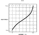
図10は横軸をデータドライバ222に入力される表示データ、縦軸をデータドライバ222から出力されるデータ電圧の絶対値としたのD-T特性を示す図である。図10で示すように、低階調や高階調側では、D-T特性の傾きが急になり、液晶駆動データDの変化に対して液晶印加電圧Vの変化が大きくなる特性となる。
(表示輝度)=(明フィールドの静的輝度T)/2+(暗フィールドの静的輝度T)/2 ・・・ (式2)
と近似できる。入力表示データをDin、明フィールド表示データをDlight、暗フィールド表示データをDdarkとすると、(式1)(式2)からγ=2.2において、

1601…階調電圧制御信号、2101…フレームメモリA、2102…メモリリードデータA、2103…フレームメモリB、2104…メモリリードデータB、2105…明フィールド変換テーブル、2106…暗フィールド変換テーブル
Claims (8)
- 外部システムから入力される表示データに応じた階調又は輝度を表示する表示装置において、
マトリックス状に配列された複数の画素を有する表示パネルと、
前記外部システムから入力される表示データを保持可能なメモリと、
中間階調の前記表示データを異なる値に変換する第1及び第2の変換回路と、
前記外部システムからの入力信号に基づき前記表示パネルを駆動するための制御信号を生成する信号生成回路と、
前記表示データに対応する電圧を前記画素へ出力する第1のドライバと、
前記電圧を供給すべき画素を走査する第2のドライバとを具備し、
前記メモリは、1フレーム期間に1回前記表示データを書き込まれ、1フレーム期間に2回前記表示データを読み出され、
前記第1の変換回路は、前記メモリから第1回目に読み出された第1の表示データと変換後の第1の表示データとの対応を示す第1のデータに基づいて、前記メモリから第1回目に読み出された第1の表示データを変換し、
前記第2の変換回路は、前記メモリから第2回目に読み出された第2の表示データと変換後の第2の表示データとの対応を示す第2のデータに基づいて、前記メモリから第2回目に読み出された第2の表示データを変換し、
前記外部システムから入力される表示データが中間階調である場合に、変換後の前記第2の表示データによる輝度は、変換後の前記第1の表示データによる輝度よりも低く、
前記第1のデータは、前記メモリから第1回目に読み出された前記第1の表示データの階調が所定の第1の階調まで大きくなるにつれ、対応する変換後の前記第1の表示データの階調が最大まで増加する変換特性を示し、
前記第2のデータは、前記メモリから第2回目に読み出された前記第2の表示データの階調が前記所定の第1の階調より低い所定の第2の階調より低ければ、変換後の前記第2の表示データの階調が最小となり、かつ、前記メモリから第2回目に読み出された第2の表示データの階調が前記所定の第2の階調から大きくなるにつれ、変換後の前記第2の表示データの階調が増加する変換特性を示し、
前記第2のドライバは、前記制御信号に従って1フレーム期間内に2回前記画素を走査し、
前記第1のドライバは、前記第2のドライバによる第1回目の走査に応じて、変換後の第1の表示データに対応する第1の電圧を前記画素へ出力し、前記第2のドライバによる第2回目の走査に応じて、変換後の第2の表示データに対応する第2の電圧を前記画素へ出力することを特徴とする表示装置。 - 請求項1に記載の表示装置において、
前記各画素での電圧の極性は、前記第2のドライバによる2回の走査毎に反転することを特徴とする表示装置。 - 請求項1に記載の表示装置において、
前記各画素は、数100秒以内の期間において、前記第1の電圧により正極性の電位が印加される回数と、前記第1の電圧により負極性の電位が印加される回数と、前記第2の電圧により正極性の電位が印加される回数と、前記第2の電圧により負極性の電位が印加される回数とが等しいことを特徴とする表示装置。 - 請求項1に記載の表示装置において、
前記外部システムからの要求に応じて、前記第1の変換回路の変換設定値及び前記第2の変換回路の変換設定値とを変更することを特徴とする表示装置。 - 請求項1に記載の表示装置において、
前記第1及び第2の変換回路は、1フレーム期間前の表示データに応じて現在のフレーム期間の表示データを変換し、
前記現在のフレーム期間の表示データと前記1フレーム期間前の表示データとが等しい場合にも、前記現在のフレーム期間の変換後の前記第1の表示データによる輝度は、前記現在のフレーム期間の変換後の前記第2の表示データによる輝度に比較して等しい若しくは大きく、
前記第1のドライバは、前記現在のフレーム期間の表示データが等しい場合の表度が前記1フレーム期間前の表示データに関わらず略等しくなるよう変換された第1及び第2の表示データに基づき前記第1の電圧及び前記第2の電圧を前記画素へ出力することを特徴とする表示装置。 - 請求項1に記載の表示装置において、
前記第1及び第2の変換回路は、1フレーム期間前の表示データに応じて現在のフレーム期間の表示データを変換し、
前記現在のフレーム期間の表示データによる輝度が前記1フレーム期間前の表示データによる輝度より大きい場合は、前記第1の変換回路は、変換後の前記第1の表示データを大きくし、その結果得られる輝度が低い場合は、前記第2の変換回路は、変換後の前記第2の表示データを大きくし、
前記現在のフレーム期間の表示データによる輝度が前記1フレーム期間前の表示データによる輝度より小さい場合は、前記第2の変換回路は、変換後の前記第2の表示データを小さくし、その結果得られる輝度が高い場合は、前記第1の変換回路は、変換後の前記第1の表示データも小さくすることを特徴とする表示装置。 - 請求項1に記載の表示装置において、
前記第1及び第2の変換回路の何れか一方は、1フレーム期間前の表示データに応じて現在のフレーム期間の表示データを変換することを特徴とする表示装置。 - 請求項1に記載の表示装置において、
前記第2のドライバの前記第2回目の走査による画素の選択期間は、前記第2のドライバの前記第1回目の走査による画素の選択期間よりも長いことを特徴とする表示装置。
Priority Applications (7)
| Application Number | Priority Date | Filing Date | Title |
|---|---|---|---|
| JP2005219899A JP4768344B2 (ja) | 2005-05-11 | 2005-07-29 | 表示装置 |
| TW095116264A TWI336868B (en) | 2005-05-11 | 2006-05-08 | Display device |
| PCT/JP2006/309770 WO2006121188A1 (en) | 2005-05-11 | 2006-05-10 | Display device |
| CN2006800157800A CN101189652B (zh) | 2005-05-11 | 2006-05-10 | 显示装置 |
| KR1020077026205A KR100901612B1 (ko) | 2005-05-11 | 2006-05-10 | 표시 장치 |
| EP06732621A EP1880376A1 (en) | 2005-05-11 | 2006-05-10 | Display device |
| US11/913,963 US20090278869A1 (en) | 2005-05-11 | 2006-05-10 | Display Device |
Applications Claiming Priority (3)
| Application Number | Priority Date | Filing Date | Title |
|---|---|---|---|
| JP2005137986 | 2005-05-11 | ||
| JP2005137986 | 2005-05-11 | ||
| JP2005219899A JP4768344B2 (ja) | 2005-05-11 | 2005-07-29 | 表示装置 |
Related Child Applications (1)
| Application Number | Title | Priority Date | Filing Date |
|---|---|---|---|
| JP2011028417A Division JP2011141557A (ja) | 2005-05-11 | 2011-02-14 | 表示装置 |
Publications (2)
| Publication Number | Publication Date |
|---|---|
| JP2006343706A JP2006343706A (ja) | 2006-12-21 |
| JP4768344B2 true JP4768344B2 (ja) | 2011-09-07 |
Family
ID=36652562
Family Applications (1)
| Application Number | Title | Priority Date | Filing Date |
|---|---|---|---|
| JP2005219899A Active JP4768344B2 (ja) | 2005-05-11 | 2005-07-29 | 表示装置 |
Country Status (6)
| Country | Link |
|---|---|
| US (1) | US20090278869A1 (ja) |
| EP (1) | EP1880376A1 (ja) |
| JP (1) | JP4768344B2 (ja) |
| KR (1) | KR100901612B1 (ja) |
| TW (1) | TWI336868B (ja) |
| WO (1) | WO2006121188A1 (ja) |
Cited By (1)
| Publication number | Priority date | Publication date | Assignee | Title |
|---|---|---|---|---|
| JP2006343707A (ja) * | 2005-05-11 | 2006-12-21 | Hitachi Displays Ltd | 表示装置 |
Families Citing this family (42)
| Publication number | Priority date | Publication date | Assignee | Title |
|---|---|---|---|---|
| JP2006349952A (ja) * | 2005-06-15 | 2006-12-28 | Sony Corp | 画像表示装置及び方法 |
| KR101146408B1 (ko) * | 2005-09-09 | 2012-05-17 | 엘지디스플레이 주식회사 | 표시장치와 그 구동방법 |
| JP5110788B2 (ja) * | 2005-11-21 | 2012-12-26 | 株式会社ジャパンディスプレイイースト | 表示装置 |
| JP2007324763A (ja) * | 2006-05-30 | 2007-12-13 | Toshiba Corp | テレビジョン受像装置及びテレビジョン受像方法 |
| US8106865B2 (en) | 2006-06-02 | 2012-01-31 | Semiconductor Energy Laboratory Co., Ltd. | Display device and driving method thereof |
| JP5068048B2 (ja) * | 2006-09-13 | 2012-11-07 | 株式会社ジャパンディスプレイイースト | 表示装置 |
| JP2008111910A (ja) * | 2006-10-30 | 2008-05-15 | Mitsubishi Electric Corp | 映像処理回路および映像表示装置 |
| JP5174363B2 (ja) * | 2006-12-08 | 2013-04-03 | 株式会社ジャパンディスプレイイースト | 表示システム |
| JP2008164721A (ja) * | 2006-12-27 | 2008-07-17 | Hitachi Displays Ltd | 表示装置 |
| US8736535B2 (en) | 2007-03-29 | 2014-05-27 | Nlt Technologies, Ltd. | Hold type image display system |
| JP2008268886A (ja) * | 2007-03-29 | 2008-11-06 | Nec Lcd Technologies Ltd | 画像表示装置 |
| CN101285949B (zh) * | 2007-04-13 | 2010-07-14 | 群康科技(深圳)有限公司 | 液晶显示装置驱动方法 |
| JP2008262105A (ja) * | 2007-04-13 | 2008-10-30 | ▲ぎょく▼瀚科技股▲ふん▼有限公司 | ディスプレーのマルチフレーム極性反転オーバードライブ方法 |
| JP2009003421A (ja) * | 2007-05-21 | 2009-01-08 | Victor Co Of Japan Ltd | 映像信号表示装置及び映像信号再生方法 |
| US7929000B2 (en) * | 2007-05-28 | 2011-04-19 | Sharp Kabushiki Kaisha | Image display device |
| JP5160836B2 (ja) * | 2007-08-08 | 2013-03-13 | ルネサスエレクトロニクス株式会社 | テレビジョン受像機 |
| JP2009058784A (ja) | 2007-08-31 | 2009-03-19 | Hitachi Displays Ltd | 表示装置 |
| WO2009055328A2 (en) * | 2007-10-25 | 2009-04-30 | Marvell World Trade Ltd. | Motion-adaptive alternating gamma drive for a liquid crystal display |
| JP2009128504A (ja) * | 2007-11-21 | 2009-06-11 | Canon Inc | 液晶表示装置 |
| FR2925813A1 (fr) * | 2007-12-20 | 2009-06-26 | Thomson Licensing Sas | Procede d'affichage d'image video pour reduire les effets de flou et de double contour et dispositif mettant en oeuvre ce procede |
| JP5276404B2 (ja) | 2008-10-03 | 2013-08-28 | 株式会社ジャパンディスプレイ | 表示装置 |
| KR101494451B1 (ko) * | 2008-11-18 | 2015-02-16 | 삼성디스플레이 주식회사 | 표시 장치 및 이의 구동 방법 |
| JP2010181616A (ja) * | 2009-02-05 | 2010-08-19 | Canon Inc | 表示装置及び表示方法 |
| JP5566048B2 (ja) | 2009-04-28 | 2014-08-06 | キヤノン株式会社 | 表示装置及びその制御方法 |
| JP2010276968A (ja) * | 2009-05-29 | 2010-12-09 | Canon Inc | 画像表示装置および画像表示方法 |
| KR20100132855A (ko) | 2009-06-10 | 2010-12-20 | 삼성에스디아이 주식회사 | 발광 장치 및 그 구동 방법 |
| JP5538849B2 (ja) * | 2009-12-08 | 2014-07-02 | キヤノン株式会社 | 画像表示装置、画像表示方法 |
| JP5381930B2 (ja) * | 2010-08-20 | 2014-01-08 | 株式会社Jvcケンウッド | 映像制御装置および映像制御方法 |
| US8675061B2 (en) * | 2010-11-01 | 2014-03-18 | Richard D. Balentine | Digital video projection display system |
| US9886899B2 (en) * | 2011-05-17 | 2018-02-06 | Ignis Innovation Inc. | Pixel Circuits for AMOLED displays |
| NL2008316C2 (en) * | 2012-02-20 | 2013-08-21 | Ambianti B V | Adaptable building panel with electric devices. |
| KR20140000458A (ko) * | 2012-06-22 | 2014-01-03 | 삼성디스플레이 주식회사 | 표시 장치 및 그 구동 방법 |
| TWI490619B (zh) * | 2013-02-25 | 2015-07-01 | Sipix Technology Inc | 電泳顯示器 |
| JP5963942B2 (ja) | 2013-03-05 | 2016-08-03 | 三菱電機株式会社 | 表示装置の映像信号制御方法および映像信号制御装置 |
| KR20150082816A (ko) * | 2014-01-08 | 2015-07-16 | 삼성디스플레이 주식회사 | 표시 패널의 구동 방법 및 이를 수행하기 위한 표시 장치 |
| CN106461990B (zh) * | 2014-06-04 | 2018-03-20 | 堺显示器制品株式会社 | 液晶显示装置以及显示方法 |
| CN104077988B (zh) * | 2014-06-18 | 2016-09-21 | 京东方科技集团股份有限公司 | 驱动信号产生电路、方法和 3d 显示装置 |
| KR102328841B1 (ko) | 2014-12-24 | 2021-11-19 | 엘지디스플레이 주식회사 | 유기 발광 다이오드 표시장치와 그 구동 방법 |
| JP6611576B2 (ja) * | 2015-11-30 | 2019-11-27 | キヤノン株式会社 | 画像処理装置および画像処理方法 |
| US11804197B1 (en) | 2020-08-28 | 2023-10-31 | Apple Inc. | Optical systems having overdriven fLCOS display panels |
| CN112233623A (zh) * | 2020-10-13 | 2021-01-15 | Tcl华星光电技术有限公司 | 显示装置及其控制方法 |
| KR20220100759A (ko) | 2021-01-08 | 2022-07-18 | 삼성디스플레이 주식회사 | 복수의 표시 패널들을 가지는 타일드 표시 장치 |
Family Cites Families (22)
| Publication number | Priority date | Publication date | Assignee | Title |
|---|---|---|---|---|
| JP3229250B2 (ja) * | 1997-09-12 | 2001-11-19 | インターナショナル・ビジネス・マシーンズ・コーポレーション | 液晶表示装置における画像表示方法及び液晶表示装置 |
| JPH1195251A (ja) * | 1997-09-19 | 1999-04-09 | Sony Corp | 液晶表示装置 |
| FR2785076B1 (fr) * | 1998-10-23 | 2002-11-15 | Thomson Multimedia Sa | Procede d'adressage pour ecran a plasma base sur un adressage separe des lignes paires et impaires |
| US6473117B1 (en) * | 1999-08-24 | 2002-10-29 | Canon Kabushiki Kaisha | Driving method for liquid crystal device |
| EP1962262A3 (en) * | 2000-03-30 | 2010-03-17 | Seiko Epson Corporation | Display device with data memory capability |
| JP2001343949A (ja) * | 2000-06-01 | 2001-12-14 | Fujitsu General Ltd | プロジェクタによる映像表示装置 |
| JP3870899B2 (ja) * | 2000-10-03 | 2007-01-24 | セイコーエプソン株式会社 | 画像処理方法、画像処理装置、電子機器、画像処理プログラムおよび当該プログラムを記録した記録媒体 |
| JP2003050569A (ja) * | 2000-11-30 | 2003-02-21 | Hitachi Ltd | 液晶表示装置 |
| KR100748840B1 (ko) * | 2001-02-05 | 2007-08-13 | 마쯔시다덴기산교 가부시키가이샤 | 액정표시장치와 그 구동방법 |
| JP3660610B2 (ja) | 2001-07-10 | 2005-06-15 | 株式会社東芝 | 画像表示方法 |
| US7265741B2 (en) * | 2002-01-21 | 2007-09-04 | Matsushita Electric Industrial Co., Ltd. | Display apparatus and display apparatus drive method |
| JP2003241721A (ja) * | 2002-02-20 | 2003-08-29 | Fujitsu Display Technologies Corp | 液晶パネルの表示制御装置および液晶表示装置 |
| JP3653506B2 (ja) * | 2002-03-20 | 2005-05-25 | 株式会社日立製作所 | 表示装置及びその駆動方法 |
| JP2003302947A (ja) * | 2002-04-10 | 2003-10-24 | Seiko Epson Corp | 電気光学装置及びその駆動方法 |
| JP2005006275A (ja) * | 2002-11-22 | 2005-01-06 | Matsushita Electric Ind Co Ltd | 補間フレーム作成装置、補間フレーム作成方法、および補間フレーム作成プログラム |
| EP1422928A3 (en) * | 2002-11-22 | 2009-03-11 | Panasonic Corporation | Motion compensated interpolation of digital video signals |
| JP4079793B2 (ja) * | 2003-02-07 | 2008-04-23 | 三洋電機株式会社 | 表示方法、表示装置およびそれに利用可能なデータ書込回路 |
| JP4653944B2 (ja) * | 2003-06-30 | 2011-03-16 | 日立プラズマディスプレイ株式会社 | 多階調表示装置 |
| JP4103740B2 (ja) * | 2003-09-10 | 2008-06-18 | セイコーエプソン株式会社 | 画像表示装置、画像表示方法及び画像表示プログラム |
| JP4176605B2 (ja) * | 2003-09-29 | 2008-11-05 | 株式会社デジタル | 表示信号変換装置 |
| JP2005173387A (ja) * | 2003-12-12 | 2005-06-30 | Nec Corp | 画像処理方法、表示装置の駆動方法及び表示装置 |
| JP2004355017A (ja) * | 2004-07-27 | 2004-12-16 | Toshiba Corp | 液晶表示装置及びその駆動方法 |
-
2005
- 2005-07-29 JP JP2005219899A patent/JP4768344B2/ja active Active
-
2006
- 2006-05-08 TW TW095116264A patent/TWI336868B/zh not_active IP Right Cessation
- 2006-05-10 US US11/913,963 patent/US20090278869A1/en not_active Abandoned
- 2006-05-10 KR KR1020077026205A patent/KR100901612B1/ko not_active IP Right Cessation
- 2006-05-10 EP EP06732621A patent/EP1880376A1/en not_active Withdrawn
- 2006-05-10 WO PCT/JP2006/309770 patent/WO2006121188A1/en active Application Filing
Cited By (1)
| Publication number | Priority date | Publication date | Assignee | Title |
|---|---|---|---|---|
| JP2006343707A (ja) * | 2005-05-11 | 2006-12-21 | Hitachi Displays Ltd | 表示装置 |
Also Published As
| Publication number | Publication date |
|---|---|
| TW200707368A (en) | 2007-02-16 |
| US20090278869A1 (en) | 2009-11-12 |
| KR100901612B1 (ko) | 2009-06-08 |
| WO2006121188A1 (en) | 2006-11-16 |
| EP1880376A1 (en) | 2008-01-23 |
| JP2006343706A (ja) | 2006-12-21 |
| TWI336868B (en) | 2011-02-01 |
| KR20080007251A (ko) | 2008-01-17 |
Similar Documents
| Publication | Publication Date | Title |
|---|---|---|
| JP4768344B2 (ja) | 表示装置 | |
| JP4218249B2 (ja) | 表示装置 | |
| US7161576B2 (en) | Matrix-type display device | |
| JP5220268B2 (ja) | 表示装置 | |
| KR100859391B1 (ko) | 표시 장치 | |
| US8054321B2 (en) | Display and driving method thereof | |
| US20070195028A1 (en) | Display device | |
| WO2013069515A1 (ja) | 表示装置およびその駆動方法 | |
| JPWO2006100906A1 (ja) | 画像表示装置、画像表示モニター、およびテレビジョン受像機 | |
| US20080246784A1 (en) | Display device | |
| JP2007271842A (ja) | 表示装置 | |
| US20080246709A1 (en) | Display device | |
| JP2011141557A (ja) | 表示装置 | |
| JP2008076433A (ja) | 表示装置 | |
| KR101365896B1 (ko) | 액정표시장치 및 그의 구동방법 | |
| JP2009237594A (ja) | 画像処理方法及びそれを用いた液晶表示装置 | |
| JP4908985B2 (ja) | 表示装置 | |
| JP2009237323A (ja) | 液晶表示装置 | |
| KR20080063435A (ko) | 표시 장치 및 그 구동 방법 | |
| JP5068048B2 (ja) | 表示装置 | |
| JP2009162943A (ja) | 液晶表示装置 |
Legal Events
| Date | Code | Title | Description |
|---|---|---|---|
| A621 | Written request for application examination |
Free format text: JAPANESE INTERMEDIATE CODE: A621 Effective date: 20070803 |
|
| A521 | Request for written amendment filed |
Free format text: JAPANESE INTERMEDIATE CODE: A523 Effective date: 20070803 |
|
| RD02 | Notification of acceptance of power of attorney |
Free format text: JAPANESE INTERMEDIATE CODE: A7422 Effective date: 20100127 |
|
| RD04 | Notification of resignation of power of attorney |
Free format text: JAPANESE INTERMEDIATE CODE: A7424 Effective date: 20100302 |
|
| A131 | Notification of reasons for refusal |
Free format text: JAPANESE INTERMEDIATE CODE: A131 Effective date: 20100921 |
|
| A521 | Request for written amendment filed |
Free format text: JAPANESE INTERMEDIATE CODE: A523 Effective date: 20101118 |
|
| A131 | Notification of reasons for refusal |
Free format text: JAPANESE INTERMEDIATE CODE: A131 Effective date: 20101214 |
|
| A711 | Notification of change in applicant |
Free format text: JAPANESE INTERMEDIATE CODE: A712 Effective date: 20110112 |
|
| A521 | Request for written amendment filed |
Free format text: JAPANESE INTERMEDIATE CODE: A523 Effective date: 20110209 |
|
| A131 | Notification of reasons for refusal |
Free format text: JAPANESE INTERMEDIATE CODE: A131 Effective date: 20110308 |
|
| A521 | Request for written amendment filed |
Free format text: JAPANESE INTERMEDIATE CODE: A523 Effective date: 20110427 |
|
| TRDD | Decision of grant or rejection written | ||
| A01 | Written decision to grant a patent or to grant a registration (utility model) |
Free format text: JAPANESE INTERMEDIATE CODE: A01 Effective date: 20110531 |
|
| A01 | Written decision to grant a patent or to grant a registration (utility model) |
Free format text: JAPANESE INTERMEDIATE CODE: A01 |
|
| A61 | First payment of annual fees (during grant procedure) |
Free format text: JAPANESE INTERMEDIATE CODE: A61 Effective date: 20110616 |
|
| R150 | Certificate of patent or registration of utility model |
Free format text: JAPANESE INTERMEDIATE CODE: R150 Ref document number: 4768344 Country of ref document: JP Free format text: JAPANESE INTERMEDIATE CODE: R150 |
|
| FPAY | Renewal fee payment (event date is renewal date of database) |
Free format text: PAYMENT UNTIL: 20140624 Year of fee payment: 3 |
|
| R250 | Receipt of annual fees |
Free format text: JAPANESE INTERMEDIATE CODE: R250 |
|
| R250 | Receipt of annual fees |
Free format text: JAPANESE INTERMEDIATE CODE: R250 |
|
| R250 | Receipt of annual fees |
Free format text: JAPANESE INTERMEDIATE CODE: R250 |
|
| R250 | Receipt of annual fees |
Free format text: JAPANESE INTERMEDIATE CODE: R250 |
|
| R250 | Receipt of annual fees |
Free format text: JAPANESE INTERMEDIATE CODE: R250 |
|
| R250 | Receipt of annual fees |
Free format text: JAPANESE INTERMEDIATE CODE: R250 |
|
| R250 | Receipt of annual fees |
Free format text: JAPANESE INTERMEDIATE CODE: R250 |
|
| R250 | Receipt of annual fees |
Free format text: JAPANESE INTERMEDIATE CODE: R250 |
|
| S531 | Written request for registration of change of domicile |
Free format text: JAPANESE INTERMEDIATE CODE: R313531 |
|
| S533 | Written request for registration of change of name |
Free format text: JAPANESE INTERMEDIATE CODE: R313533 |
|
| R350 | Written notification of registration of transfer |
Free format text: JAPANESE INTERMEDIATE CODE: R350 |
|
| R250 | Receipt of annual fees |
Free format text: JAPANESE INTERMEDIATE CODE: R250 |
|
| R250 | Receipt of annual fees |
Free format text: JAPANESE INTERMEDIATE CODE: R250 |
|
| S111 | Request for change of ownership or part of ownership |
Free format text: JAPANESE INTERMEDIATE CODE: R313117 |
|
| R350 | Written notification of registration of transfer |
Free format text: JAPANESE INTERMEDIATE CODE: R350 |
|
| R250 | Receipt of annual fees |
Free format text: JAPANESE INTERMEDIATE CODE: R250 |