JP4713280B2 - Reference voltage generation circuit and constant voltage circuit using the reference voltage generation circuit - Google Patents
Reference voltage generation circuit and constant voltage circuit using the reference voltage generation circuit Download PDFInfo
- Publication number
- JP4713280B2 JP4713280B2 JP2005252011A JP2005252011A JP4713280B2 JP 4713280 B2 JP4713280 B2 JP 4713280B2 JP 2005252011 A JP2005252011 A JP 2005252011A JP 2005252011 A JP2005252011 A JP 2005252011A JP 4713280 B2 JP4713280 B2 JP 4713280B2
- Authority
- JP
- Japan
- Prior art keywords
- field effect
- effect transistor
- reference voltage
- voltage
- ratio
- Prior art date
- Legal status (The legal status is an assumption and is not a legal conclusion. Google has not performed a legal analysis and makes no representation as to the accuracy of the status listed.)
- Active
Links
- 230000005669 field effect Effects 0.000 claims description 278
- 239000000758 substrate Substances 0.000 claims description 28
- 230000007423 decrease Effects 0.000 claims description 12
- 238000010586 diagram Methods 0.000 description 20
- 230000001360 synchronised effect Effects 0.000 description 12
- 238000000034 method Methods 0.000 description 7
- 230000010355 oscillation Effects 0.000 description 5
- 239000012535 impurity Substances 0.000 description 4
- 239000003990 capacitor Substances 0.000 description 3
- 238000001514 detection method Methods 0.000 description 2
- 230000000694 effects Effects 0.000 description 2
- 206010037660 Pyrexia Diseases 0.000 description 1
- 230000003321 amplification Effects 0.000 description 1
- 238000013459 approach Methods 0.000 description 1
- 239000006185 dispersion Substances 0.000 description 1
- 238000009499 grossing Methods 0.000 description 1
- 239000000203 mixture Substances 0.000 description 1
- 238000003199 nucleic acid amplification method Methods 0.000 description 1
- 229920006395 saturated elastomer Polymers 0.000 description 1
Images


Classifications
-
- G—PHYSICS
- G11—INFORMATION STORAGE
- G11C—STATIC STORES
- G11C5/00—Details of stores covered by group G11C11/00
- G11C5/14—Power supply arrangements, e.g. power down, chip selection or deselection, layout of wirings or power grids, or multiple supply levels
- G11C5/147—Voltage reference generators, voltage or current regulators; Internally lowered supply levels; Compensation for voltage drops
Landscapes
- Engineering & Computer Science (AREA)
- Power Engineering (AREA)
- Control Of Electrical Variables (AREA)
- Semiconductor Integrated Circuits (AREA)
- Metal-Oxide And Bipolar Metal-Oxide Semiconductor Integrated Circuits (AREA)
- Continuous-Control Power Sources That Use Transistors (AREA)
- Dc-Dc Converters (AREA)
Description
本発明は、基準電圧発生回路及び基準電圧発生回路を使用した定電圧回路に関し、特に、2つの電界効果トランジスタのゲート電極の仕事関数差の原理を用いた基準電圧発生回路及び基準電圧発生回路を使用した定電圧回路に関する。 The present invention relates to a reference voltage generation circuit and a constant voltage circuit using the reference voltage generation circuit, and more particularly to a reference voltage generation circuit and a reference voltage generation circuit using the principle of work function difference between gate electrodes of two field effect transistors. It relates to the constant voltage circuit used.
従来、図19で示すように、デプレッション型の電界効果トランジスタとエンハンスメント型の電界効果トランジスタを直列に接続し、これらの電界効果トランジスタのしきい値電圧Vthの差を基準電圧Vrefとして取り出すようにした基準電圧発生回路があった(例えば、特許文献1参照。)。
図19において、トランジスタ105はデプレッション型のn型電界効果トランジスタであり、トランジスタ107はエンハンスメント型のn型電界効果トランジスタである。
電界効果トランジスタは飽和状態では、ドレイン電流idは、下記(a)式のようになる。
id=K×(Vgs−Vth)2………………(a)
但し、前記(a)式において、Kは導電係数を、Vgsはゲート‐ソース間電圧をそれぞれ示している。
Conventionally, as shown in FIG. 19, a depletion type field effect transistor and an enhancement type field effect transistor are connected in series, and the difference between the threshold voltages Vth of these field effect transistors is taken out as a reference voltage Vref. There was a reference voltage generation circuit (see, for example, Patent Document 1).
In FIG. 19, a
When the field effect transistor is saturated, the drain current id is expressed by the following equation (a).
id = K × (Vgs−Vth) 2 ……………… (a)
In the equation (a), K represents a conductivity coefficient, and Vgs represents a gate-source voltage.
トランジスタ105と107には同じ電流が流れることから、ノード108の電圧Vgs7は、下記(b)式のようになる。
Vgs7=Vth7−(K5/K7)1/2×Vth5………………(b)
但し、前記(b)式において、K5はトランジスタ105の導電係数を、K7はトランジスタ107の導電係数を、Vth5はトランジスタ105のしきい値電圧を、Vth7はトランジスタ107のしきい値電圧をそれぞれ示している。
ここで、導電係数K5とK7が等しくなるようにすると、前記(b)式は下記(c)式のようになる。
Vgs7=Vth7−Vth5………………(c)
このように、ノード108の電圧Vgs7は、トランジスタ105と107の各しきい値電圧の差になって基準電圧Vrefをなし、その様子を図20に示す。
Since the same current flows through the
Vgs7 = Vth7− (K5 / K7) 1/2 × Vth5 (b)
In the equation (b), K5 represents the conductivity coefficient of the
Here, when the conductivity coefficients K5 and K7 are made equal, the equation (b) becomes the following equation (c).
Vgs7 = Vth7−Vth5 (c)
As described above, the voltage Vgs7 at the
一方、図21に示すように、n型ゲートを持つトランジスタとp型ゲートを持つトランジスタにそれぞれ定電流を流して、これらトランジスタのしきい値電圧の差を基準電圧Vrefとして取り出す基準電圧発生回路があった(例えば、特許文献2参照。)。
図21では、導電係数Kがほぼ等しいn型ゲートを持つトランジスタT1とp型ゲートを持つトランジスタT2にそれぞれ定電流Ioを流すことにより、定電流Ioは、下記(d)式で示すことができる。
Io=K×(V1−Vth1)2=K×(V2−Vth2)2………(d)
但し、前記(d)式において、V1はトランジスタT1のドレイン‐ソース間電圧を、Vth1はトランジスタT1のしきい値電圧を、V2はトランジスタT2のドレイン‐ソース間電圧を、Vth2はトランジスタT2のしきい値電圧をそれぞれ示している。
On the other hand, as shown in FIG. 21, there is a reference voltage generating circuit for supplying a constant current to each of a transistor having an n-type gate and a transistor having a p-type gate and taking out a difference between threshold voltages of these transistors as a reference voltage Vref. (For example, refer to Patent Document 2).
In FIG. 21, the constant current Io can be expressed by the following equation (d) by flowing a constant current Io through a transistor T1 having an n-type gate and a transistor T2 having a p-type gate having substantially the same conductivity coefficient K. .
Io = K × (V1−Vth1) 2 = K × (V2−Vth2) 2 (d)
In the equation (d), V1 is the drain-source voltage of the transistor T1, Vth1 is the threshold voltage of the transistor T1, V2 is the drain-source voltage of the transistor T2, and Vth2 is the threshold voltage of the transistor T2. Each threshold voltage is shown.
前記(d)式より、
V2−V1=Vth2−Vth1
となり、トランジスタT1及びT2のドレイン電圧の差を取り出すことにより、トランジスタT1及びT2のしきい値電圧の差を取り出すことができる。
図22に、ドレインの電圧差を取り出す回路図を示す(例えば、特許文献2参照。)。図22の回路では、デプレッション型とエンハンスメント型の2種類のトランジスタを使用するのではなく、トランジスタのゲート電極の組成を変えることにより、トランジスタT1とT2のしきい値電圧を異なる値にしている。
V2-V1 = Vth2-Vth1
Thus, by extracting the difference between the drain voltages of the transistors T1 and T2, the difference between the threshold voltages of the transistors T1 and T2 can be extracted.
FIG. 22 shows a circuit diagram for extracting the voltage difference between the drains (see, for example, Patent Document 2). In the circuit of FIG. 22, the threshold voltages of the transistors T1 and T2 are set to different values by changing the composition of the gate electrode of the transistor, instead of using two types of transistors of depletion type and enhancement type.
しかし、図21の回路には次のような3つの課題があった。
第1の課題は、デプレッション型とエンハンスメント型の2種類のトランジスタを使用しているため、プロセス変動により、各トランジスタのしきい値電圧Vthはそれぞれ独立して変動してしまい、基準電圧Vrefの初期精度が悪くなってしまうということである。図23に示すように、各トランジスタのしきい値電圧VthのばらつきをΔVth5とΔVth7とすると、基準電圧Vrefの変動は、−(ΔVth5+ΔVth7)から(ΔVth5+ΔVth7)まで変動することになる。例えば、Vth5=−0.5V、Vth7=0.5V、ΔVth5=ΔVth7=0.15Vとすると、基準電圧Vrefは、0.7V〜1.3V(±30%)まで変動することになり、基準電圧Vrefの変動が大きいという問題があった。
However, the circuit of FIG. 21 has the following three problems.
The first problem is that since two types of transistors, a depletion type and an enhancement type, are used, the threshold voltage Vth of each transistor fluctuates independently due to process variation, and the initial value of the reference voltage Vref The accuracy will be worse. As shown in FIG. 23, when the variation of the threshold voltage Vth of each transistor is ΔVth5 and ΔVth7, the variation of the reference voltage Vref varies from − (ΔVth5 + ΔVth7) to (ΔVth5 + ΔVth7). For example, when Vth5 = −0.5V, Vth7 = 0.5V, and ΔVth5 = ΔVth7 = 0.15V, the reference voltage Vref varies from 0.7V to 1.3V (± 30%). There was a problem that the fluctuation of the voltage Vref was large.
第2の課題は、デプレッション型とエンハンスメント型の2種類のトランジスタを使用していることから、これらトランジスタのチャネル領域のポテンシャル差の温度特性が同一でないため、温度特性が悪くなってしまうということである。そこで、温度特性を改善するために、トランジスタ105のチャネル幅Wとチャネル長Lの比S5(=W/L)とトランジスタ107のチャネル幅Wとチャネル長Lの比S7(=W/L)の比(S5/S7)を調整してもせいぜい約300ppm/℃にしかならなかった。このように、基準電圧Vrefの温度特性が大きいという問題があった。
The second problem is that, since two types of transistors, a depletion type and an enhancement type, are used, the temperature characteristics of the potential difference in the channel region of these transistors are not the same, so that the temperature characteristics deteriorate. is there. Therefore, in order to improve temperature characteristics, the ratio S5 (= W / L) of the channel width W and the channel length L of the
第3の課題は、各トランジスタ105及び107のソース‐ドレイン間電圧Vds5及びVds7が、
Vds5=VCC−Vg7
Vds7=Vg7
となる。このため、電源電圧VCCが変動すると、トランジスタ105のソース‐ドレイン間電圧Vds5も変動してしまい、基準電圧Vrefが電源電圧VCCの変動に応じて変動することである。図24に示すように、電源電圧VCCが大きくなると、トランジスタ105のゲート‐ソース間電圧Vgsとドレイン電流idとの関係を示した曲線がずれてしまい、基準電圧VrefがΔVrefだけ大きくなるという問題があった。
The third problem is that the source-drain voltages Vds5 and Vds7 of the
Vds5 = VCC-Vg7
Vds7 = Vg7
It becomes. Therefore, when the power supply voltage VCC varies, the source-drain voltage Vds5 of the
一方、図22の回路では、前記第1及び第2の各課題を解決することができるが、定電流源として抵抗を使用していることから、前記第3の課題を解決することができなかった。 On the other hand, the circuit of FIG. 22 can solve the first and second problems, but cannot use the resistor as a constant current source, and therefore cannot solve the third problem. It was.
本発明は、上記のような問題を解決するためになされたものであり、プロセス変動、温度変動及び電源電圧変動による基準電圧のばらつきを低減させることができる基準電圧発生回路及び基準電圧発生回路を使用した定電圧回路を得ることを目的とする。 The present invention has been made to solve the above-described problems, and provides a reference voltage generation circuit and a reference voltage generation circuit that can reduce variations in the reference voltage due to process variations, temperature variations, and power supply voltage variations. It aims at obtaining the used constant voltage circuit.
この発明に係る基準電圧発生回路は、所定の基準電圧を生成して出力端から出力する基準電圧発生回路において、
一端が所定の電源電圧に接続された、デプレッション型のnチャネル型電界効果トランジスタである第1の電界効果トランジスタと、
一端が該第1の電界効果トランジスタの他端に接続された、高濃度n型ゲートを有する第2の電界効果トランジスタと、
一端が該第2の電界効果トランジスタの他端に接続され、他端が接地電圧に接続された、高濃度p型ゲートを有する第3の電界効果トランジスタと、
を備え、
前記第1の電界効果トランジスタのゲートは、該第1の電界効果トランジスタと前記第2の電界効果トランジスタとの接続部に接続されると共に、前記第1及び第3の各電界効果トランジスタのサブストレートゲートは、それぞれ接地電圧に接続され、前記第2の電界効果トランジスタのゲート及びサブストレートゲート、並びに前記第3の電界効果トランジスタのゲートは、前記出力端をなす第2及び第3の各電界効果トランジスタの接続部にそれぞれ接続され、前記第2及び第3の各電界効果トランジスタは、ゲート‐ソース間電圧が正又は負の同一極性の温度特性を有するように、ゲート‐ソース間電圧とドレイン電流との関係が設定されると共に、前記基準電圧の温度特性の絶対値が低下するようなチャネル幅とチャネル長との比にそれぞれ形成されるものである。
A reference voltage generation circuit according to the present invention is a reference voltage generation circuit that generates a predetermined reference voltage and outputs the reference voltage from an output terminal.
A first field effect transistor that is a depletion type n-channel field effect transistor, one end of which is connected to a predetermined power supply voltage;
A second field effect transistor having a high concentration n-type gate, one end connected to the other end of the first field effect transistor;
A third field effect transistor having a high-concentration p-type gate having one end connected to the other end of the second field effect transistor and the other end connected to a ground voltage;
With
A gate of the first field effect transistor is connected to a connection portion between the first field effect transistor and the second field effect transistor, and a substrate of each of the first and third field effect transistors. The gates are respectively connected to a ground voltage, and the gates and the substrate gates of the second field effect transistors and the gates of the third field effect transistors are the second and third field effects forming the output terminal, respectively. Each of the second and third field effect transistors is connected to a connection portion of the transistor, and the gate-source voltage and the drain current are set such that the gate-source voltage has a temperature characteristic of the same polarity of positive or negative. with relationship is set between, on the ratio between the channel width and channel length as the absolute value decreases the temperature characteristics of the reference voltage Are those respectively formed.
また、前記第3の電界効果トランジスタは、チャネル幅とチャネル長との比S3が、第2の電界効果トランジスタのチャネル幅とチャネル長との比S2未満であるようにした。 In the third field effect transistor, the ratio S3 between the channel width and the channel length is less than the ratio S2 between the channel width and the channel length of the second field effect transistor.
具体的には、前記第2及び第3の各電界効果トランジスタは、チャネル幅とチャネル長との比S3とS2との比S3/S2が0.5〜0.67になるようにそれぞれ形成されるようにした。 Specifically, each of the second and third field effect transistors is formed such that the ratio S3 / S2 of the ratio S3 to S2 of the channel width to the channel length is 0.5 to 0.67. It was to so.
更に具体的には、前記第2及び第3の各電界効果トランジスタは、チャネル幅とチャネル長との比S3とS2との比S3/S2が0.54〜0.58になるようにそれぞれ形成されるようにした。 More specifically, the second and third field effect transistors are formed so that the ratio S3 / S2 of the channel width / channel length ratio S3 / S2 is 0.54 to 0.58. It was made to be.
また、この発明に係る基準電圧発生回路は、所定の基準電圧を生成して出力端から出力する基準電圧発生回路において、
一端が所定の電源電圧に接続された、デプレッション型のnチャネル型電界効果トランジスタである第1の電界効果トランジスタと、
一端が該第1の電界効果トランジスタの他端に接続された、高濃度n型ゲートを有する第2の電界効果トランジスタと、
一端が該第2の電界効果トランジスタの他端に接続され、他端が接地電圧に接続された、高濃度p型ゲートを有する第3の電界効果トランジスタと、
を備え、
前記第1の電界効果トランジスタのゲートは、該第1の電界効果トランジスタと前記第2の電界効果トランジスタとの接続部に接続されると共に、前記第1から第3の各電界効果トランジスタのサブストレートゲートは、それぞれ接地電圧に接続され、前記第2及び第3の各電界効果トランジスタのゲートは、前記出力端をなす前記第2及び第3の各電界効果トランジスタの接続部にそれぞれ接続され、前記第2及び第3の各電界効果トランジスタは、ゲート‐ソース間電圧が正又は負の同一極性の温度特性を有するように、ゲート‐ソース間電圧とドレイン電流との関係が設定されると共に、前記基準電圧の温度特性の絶対値が低下するようなチャネル幅とチャネル長との比にそれぞれ形成されるものである。
Further, the reference voltage generation circuit according to the present invention is a reference voltage generation circuit that generates a predetermined reference voltage and outputs it from an output terminal.
A first field effect transistor that is a depletion type n-channel field effect transistor, one end of which is connected to a predetermined power supply voltage;
A second field effect transistor having a high concentration n-type gate, one end connected to the other end of the first field effect transistor;
A third field effect transistor having a high-concentration p-type gate having one end connected to the other end of the second field effect transistor and the other end connected to a ground voltage;
With
A gate of the first field effect transistor is connected to a connection portion between the first field effect transistor and the second field effect transistor, and a substrate of each of the first to third field effect transistors. The gates are respectively connected to a ground voltage, and the gates of the second and third field effect transistors are respectively connected to connection portions of the second and third field effect transistors forming the output terminal, In each of the second and third field effect transistors, the relationship between the gate-source voltage and the drain current is set so that the gate-source voltage has a positive or negative temperature characteristic of the same polarity. The channel voltage and the channel length are respectively formed such that the absolute value of the temperature characteristic of the reference voltage decreases .
また、前記第3の電界効果トランジスタは、チャネル幅とチャネル長との比S3が、第2の電界効果トランジスタのチャネル幅とチャネル長との比S2未満であるようにした。 In the third field effect transistor, the ratio S3 between the channel width and the channel length is less than the ratio S2 between the channel width and the channel length of the second field effect transistor.
具体的には、前記第2及び第3の各電界効果トランジスタは、チャネル幅とチャネル長との比S3とS2との比S3/S2が0.35〜0.45になるようにそれぞれ形成されるようにした。 Specifically, each of the second and third field effect transistors is formed such that the ratio S3 / S2 of the channel width / channel length ratio S3 to S2 is 0.35 to 0.45. It was to so.
更に具体的には、前記第2及び第3の各電界効果トランジスタは、チャネル幅とチャネル長との比S3とS2との比S3/S2が0.37〜0.41になるようにそれぞれ形成されるようにした。 More specifically, the second and third field effect transistors are formed so that the ratio S3 / S2 of the channel width / channel length ratio S3 / S2 is 0.37 to 0.41. It was made to be.
また、この発明に係る定電圧回路は、基準電圧発生回路で生成された所定の基準電圧を基準にして、入力電圧から所定の定電圧を生成して出力する定電圧回路において、
前記基準電圧発生回路は、
一端が所定の電源電圧に接続された、デプレッション型のnチャネル型電界効果トランジスタである第1の電界効果トランジスタと、
一端が該第1の電界効果トランジスタの他端に接続された、高濃度n型ゲートを有する第2の電界効果トランジスタと、
一端が該第2の電界効果トランジスタの他端に接続され、他端が接地電圧に接続された、高濃度p型ゲートを有する第3の電界効果トランジスタと、
を備え、
前記第1の電界効果トランジスタのゲートは、該第1の電界効果トランジスタと前記第2の電界効果トランジスタとの接続部に接続されると共に、前記第1及び第3の各電界効果トランジスタのサブストレートゲートは、それぞれ接地電圧に接続され、前記第2の電界効果トランジスタのゲート及びサブストレートゲート、並びに前記第3の電界効果トランジスタのゲートは、前記基準電圧を出力する出力端をなす前記第2及び第3の各電界効果トランジスタの接続部にそれぞれ接続され、前記第2及び第3の各電界効果トランジスタは、ゲート‐ソース間電圧が正又は負の同一極性の温度特性を有するように、ゲート‐ソース間電圧とドレイン電流との関係が設定されると共に、前記基準電圧の温度特性の絶対値が低下するようなチャネル幅とチャネル長との比にそれぞれ形成されるものである。
The constant voltage circuit according to the present invention is a constant voltage circuit that generates and outputs a predetermined constant voltage from an input voltage with reference to the predetermined reference voltage generated by the reference voltage generation circuit.
The reference voltage generation circuit includes:
A first field effect transistor that is a depletion type n-channel field effect transistor, one end of which is connected to a predetermined power supply voltage;
A second field effect transistor having a high concentration n-type gate, one end connected to the other end of the first field effect transistor;
A third field effect transistor having a high-concentration p-type gate having one end connected to the other end of the second field effect transistor and the other end connected to a ground voltage;
With
A gate of the first field effect transistor is connected to a connection portion between the first field effect transistor and the second field effect transistor, and a substrate of each of the first and third field effect transistors. The gates are respectively connected to a ground voltage, and the gates and the substrate gates of the second field effect transistors and the gates of the third field effect transistors form the output terminals for outputting the reference voltage. Each of the second and third field effect transistors is connected to a connection portion of each third field effect transistor, and the second and third field effect transistors have a gate-source voltage having a temperature characteristic of the same polarity of positive or negative. A channel in which the relationship between the source voltage and the drain current is set and the absolute value of the temperature characteristic of the reference voltage is reduced. Are those formed respectively to the ratio of the channel length.
また、前記第3の電界効果トランジスタは、チャネル幅とチャネル長との比S3が、第2の電界効果トランジスタのチャネル幅とチャネル長との比S2未満であるようにした。 In the third field effect transistor, the ratio S3 between the channel width and the channel length is less than the ratio S2 between the channel width and the channel length of the second field effect transistor.
具体的には、前記第2及び第3の各電界効果トランジスタは、チャネル幅とチャネル長との比S3とS2との比S3/S2が0.5〜0.67になるようにそれぞれ形成されるようにした。 Specifically, each of the second and third field effect transistors is formed such that the ratio S3 / S2 of the ratio S3 to S2 of the channel width to the channel length is 0.5 to 0.67. It was to so.
更に具体的には、前記第2及び第3の各電界効果トランジスタは、チャネル幅とチャネル長との比S3とS2との比S3/S2が0.54〜0.58になるようにそれぞれ形成されるようにした。 More specifically, the second and third field effect transistors are formed so that the ratio S3 / S2 of the channel width / channel length ratio S3 / S2 is 0.54 to 0.58. It was made to be.
また、この発明に係る定電圧回路は、基準電圧発生回路で生成された所定の基準電圧を基準にして、入力電圧から所定の定電圧を生成して出力する定電圧回路において、
前記基準電圧発生回路は、
一端が所定の電源電圧に接続された、デプレッション型のnチャネル型電界効果トランジスタである第1の電界効果トランジスタと、
一端が該第1の電界効果トランジスタの他端に接続された、高濃度n型ゲートを有する第2の電界効果トランジスタと、
一端が該第2の電界効果トランジスタの他端に接続され、他端が接地電圧に接続された、高濃度p型ゲートを有する第3の電界効果トランジスタと、
を備え、
前記第1の電界効果トランジスタのゲートは、該第1の電界効果トランジスタと前記第2の電界効果トランジスタとの接続部に接続されると共に、前記第1から第3の各電界効果トランジスタのサブストレートゲートは、それぞれ接地電圧に接続され、前記第2及び第3の各電界効果トランジスタのゲートは、前記基準電圧を出力する出力端をなす前記第2及び第3の各電界効果トランジスタの接続部にそれぞれ接続され、前記第2及び第3の各電界効果トランジスタは、ゲート‐ソース間電圧が正又は負の同一極性の温度特性を有するように、ゲート‐ソース間電圧とドレイン電流との関係が設定されると共に、前記基準電圧の温度特性の絶対値が低下するようなチャネル幅とチャネル長との比にそれぞれ形成されるものである。
The constant voltage circuit according to the present invention is a constant voltage circuit that generates and outputs a predetermined constant voltage from an input voltage with reference to the predetermined reference voltage generated by the reference voltage generation circuit.
The reference voltage generation circuit includes:
A first field effect transistor that is a depletion type n-channel field effect transistor, one end of which is connected to a predetermined power supply voltage;
A second field effect transistor having a high concentration n-type gate, one end connected to the other end of the first field effect transistor;
A third field effect transistor having a high-concentration p-type gate having one end connected to the other end of the second field effect transistor and the other end connected to a ground voltage;
With
A gate of the first field effect transistor is connected to a connection portion between the first field effect transistor and the second field effect transistor, and a substrate of each of the first to third field effect transistors. Gates are respectively connected to a ground voltage, and gates of the second and third field effect transistors are connected to connection portions of the second and third field effect transistors that form an output terminal for outputting the reference voltage. Each of the second and third field effect transistors is connected, and the relationship between the gate-source voltage and the drain current is set so that the gate-source voltage has the same polarity of positive or negative temperature characteristics. In addition, the channel width and the channel length are formed such that the absolute value of the temperature characteristic of the reference voltage decreases .
また、前記第3の電界効果トランジスタは、チャネル幅とチャネル長との比S3が、第2の電界効果トランジスタのチャネル幅とチャネル長との比S2未満であるようにした。 In the third field effect transistor, the ratio S3 between the channel width and the channel length is less than the ratio S2 between the channel width and the channel length of the second field effect transistor.
具体的には、前記第2及び第3の各電界効果トランジスタは、チャネル幅とチャネル長との比S3とS2との比S3/S2が0.35〜0.45になるようにそれぞれ形成されるようにした。 Specifically, each of the second and third field effect transistors is formed such that the ratio S3 / S2 of the channel width / channel length ratio S3 to S2 is 0.35 to 0.45. It was to so.
更に具体的には、前記第2及び第3の各電界効果トランジスタは、チャネル幅とチャネル長との比S3とS2との比S3/S2が0.37〜0.41になるようにそれぞれ形成されるようにした。 More specifically, the second and third field effect transistors are formed so that the ratio S3 / S2 of the channel width / channel length ratio S3 / S2 is 0.37 to 0.41. It was made to be.
本発明の基準電圧発生回路及び基準電圧発生回路を使用した定電圧回路によれば、例えば、基準電圧発生回路で生成される基準電圧は、従来回路に対して、初期精度が±30%から±6%に、温度特性は300ppm/℃から40ppm/℃にそれぞれ改善され、更に電源電圧変動に対する基準電圧Vrefの変動を1/10以下に低減させることができ、プロセス変動、温度変動及び電源電圧変動による基準電圧のばらつきを低減させることができ、更に、定電圧回路においては、出力電圧のばらつきを低減させることができる。 According to the reference voltage generation circuit and the constant voltage circuit using the reference voltage generation circuit of the present invention, for example, the reference voltage generated by the reference voltage generation circuit has an initial accuracy of ± 30% to ±± 6%, temperature characteristics are improved from 300ppm / ° C to 40ppm / ° C, and the fluctuation of the reference voltage Vref with respect to the fluctuation of power supply voltage can be reduced to 1/10 or less, process fluctuation, temperature fluctuation and power supply voltage fluctuation Can reduce the variation in the reference voltage, and in the constant voltage circuit, the variation in the output voltage can be reduced.
次に、図面に示す実施の形態に基づいて、本発明を詳細に説明する。
第1の実施の形態.
図1は、本発明の第1の実施の形態における基準電圧発生回路の例を示した回路図である。
図1において、基準電圧発生回路1は、nチャネル型の電界効果トランジスタM1〜M3で構成され、電源電圧VCCと接地電圧GNDとの間に、電界効果トランジスタM1〜M3が直列に接続されている。なお、電界効果トランジスタM1は第1の電界効果トランジスタを、電界効果トランジスタM2は第2の電界効果トランジスタを、電界効果トランジスタM3は第3の電界効果トランジスタをそれぞれなす。
Next, the present invention will be described in detail based on the embodiments shown in the drawings.
First embodiment.
FIG. 1 is a circuit diagram showing an example of a reference voltage generation circuit according to the first embodiment of the present invention.
In FIG. 1, a reference
電界効果トランジスタM1は、n型基板のpウエル内に形成されたデプレッション型トランジスタであり、ゲートとソースが接続され、サブストレートゲートは接地電圧GNDに接続されている。電界効果トランジスタM2及びM3は、基板やチャネルドープの不純物濃度が等しく、n型基板のpウエル内にそれぞれ形成され、電界効果トランジスタM2は高濃度n型ゲートを持ち、電界効果トランジスタM3は高濃度p型ゲートを持つ。電界効果トランジスタM2及びM3の接続部に電界効果トランジスタM2及びM3の各ゲート並びに電界効果トランジスタM2のサブストレートゲートがそれぞれ接続されている。該接続部が基準電圧Vrefを出力する出力端をなし、電界効果トランジスタM2は定電流源をなしている。また、電界効果トランジスタM3のサブストレートゲートは接地電圧に接続されている。 The field effect transistor M1 is a depletion type transistor formed in a p-well of an n-type substrate, the gate and source are connected, and the substrate gate is connected to the ground voltage GND. The field effect transistors M2 and M3 have the same substrate and channel-doped impurity concentrations and are formed in the p-well of the n-type substrate, respectively, the field-effect transistor M2 has a high-concentration n-type gate, and the field-effect transistor M3 has a high concentration. Has a p-type gate. The gates of the field effect transistors M2 and M3 and the substrate gate of the field effect transistor M2 are connected to the connection portion of the field effect transistors M2 and M3, respectively. The connection portion serves as an output terminal for outputting the reference voltage Vref, and the field effect transistor M2 serves as a constant current source. The substrate gate of the field effect transistor M3 is connected to the ground voltage.
このような構成において、基準電圧Vrefは下記(1)式のようになる。
Vref=VthM3−(KM2/KM3)1/2×VthM2………(1)
但し、前記(1)式において、KM2は電界効果トランジスタM2の導電係数 、KM3は電界効果トランジスタM3の導電係数、VthM2は電界効果トランジスタM2のしきい値電圧、VthM3は電界効果トランジスタM3のしきい値電圧をそれぞれ示している。
電界効果トランジスタM2及びM3の導電係数が等しくなるようにすると、前記(1)式は下記(2)式のようになる。
Vref=VthM3−VthM2………………(2)
前記(2)式から、基準電圧Vrefは電界効果トランジスタM2とM3の各しきい値電圧の電圧差になる。
In such a configuration, the reference voltage Vref is expressed by the following equation (1).
Vref = VthM3− (KM2 / KM3) 1/2 × VthM2 (1)
In the equation (1), KM2 is the conductivity coefficient of the field effect transistor M2, KM3 is the conductivity coefficient of the field effect transistor M3, VthM2 is the threshold voltage of the field effect transistor M2, and VthM3 is the threshold of the field effect transistor M3. Each value voltage is shown.
When the conductivity coefficients of the field effect transistors M2 and M3 are made equal, the equation (1) becomes the following equation (2).
Vref = VthM3-VthM2 (2)
From the equation (2), the reference voltage Vref is a voltage difference between the threshold voltages of the field effect transistors M2 and M3.
次に、図2は、電界効果トランジスタM2とM3におけるゲート‐ソース間電圧Vgsとドレイン電流idとの各関係を示したそれぞれのVgs‐id特性を示している。
図2において、電界効果トランジスタM2は、ソースとゲートが接続されているため、id2のドレイン電流が流れる。電界効果トランジスタM3は、電界効果トランジスタM2と直列に接続されていることから、同様にid2の電流が流れ、このときの電界効果トランジスタM2及びM3のゲート‐ソース間電圧Vgsの電圧差が基準電圧Vrefになる。
Next, FIG. 2 shows respective Vgs-id characteristics showing respective relationships between the gate-source voltage Vgs and the drain current id in the field effect transistors M2 and M3.
In FIG. 2, since the source and gate of the field effect transistor M2 are connected, the drain current of id2 flows. Since the field effect transistor M3 is connected in series with the field effect transistor M2, the current of id2 similarly flows, and the voltage difference between the gate-source voltages Vgs of the field effect transistors M2 and M3 at this time is the reference voltage. Vref.
したがって、プロセスの変動によって、基板やチャネルドープの不純物濃度がばらついても、電界効果トランジスタM2とM3の該各濃度が同様にばらつく。このため、図3に示すように、電界効果トランジスタM2とM3の各Vgs‐id特性は、図2の関係を保ったまま、左右に移動するだけであり、基準電圧Vrefの絶対値にはほとんど影響を与えず安定した基準電圧Vrefを発生させることができる。また、実験結果からも、基準電圧Vrefのばらつきが±1%程度に収まり、基準電圧Vrefのばらつきを低減させることができる。 Therefore, even if the impurity concentration of the substrate and the channel dope varies due to process variations, the respective concentrations of the field effect transistors M2 and M3 also vary. Therefore, as shown in FIG. 3, the Vgs-id characteristics of the field effect transistors M2 and M3 only move to the left and right while maintaining the relationship of FIG. 2, and the absolute value of the reference voltage Vref is almost the same. A stable reference voltage Vref can be generated without any influence. Also, from the experimental results, the variation in the reference voltage Vref is about ± 1%, and the variation in the reference voltage Vref can be reduced.
電界効果トランジスタM2及びM3は、基板やチャネルドープの不純物濃度が等しいデプレッション型トランジスタであり、電界効果トランジスタM2は高濃度n型ゲートを持ち、電界効果トランジスタM3は高濃度p型ゲートを持つ。電界効果トランジスタM2及びM3のチャネル領域のポテンシャル差の温度特性を等しくする、すなわち前記(1)式での導電係数が等しくなるようにしても、ゲートの仕事関数差が持つ温度特性のために、得られる基準電圧Vrefは約−500ppm/℃の温度特性を持ってしまう。しかし、該温度特性は、デプレッション型とエンハンスメント型の2種類の電界効果トランジスタを使用し、ゲートの仕事関数差が持つ温度特性はないが、各電界効果トランジスタM2及びM3のチャネル領域のポテンシャル差の温度特性が同一でない図19の従来技術よりも小さい。 The field effect transistors M2 and M3 are depletion type transistors having the same substrate and channel-doped impurity concentration, the field effect transistor M2 has a high concentration n-type gate, and the field effect transistor M3 has a high concentration p-type gate. Even if the temperature characteristics of the potential difference between the channel regions of the field effect transistors M2 and M3 are made equal, that is, the conductivity coefficient in the equation (1) is made equal, the temperature characteristics of the gate work function difference are: The obtained reference voltage Vref has a temperature characteristic of about −500 ppm / ° C. However, the temperature characteristic uses two types of field effect transistors of depletion type and enhancement type, and there is no temperature characteristic of the work function difference of the gate, but the potential difference between the channel regions of the field effect transistors M2 and M3. The temperature characteristics are smaller than those of the prior art shown in FIG.
そこで、電界効果トランジスタM2のチャネル幅W2とチャネル長L2の比S2(=W2/L2)と電界効果トランジスタM3のチャネル幅W3とチャネル長L3の比S3(=W3/L3)をそれぞれ調整して、更に基準電圧Vrefの温度特性を改善させる。
図4は、S3/S2の比を変えたときの基準電圧Vrefの温度特性の実験データを示した図であり、図4では、25℃をセンターにしたときの実験データを示している。
図4において、実線はS3/S2=1.00のときを示しており、このときの基準電圧Vrefの温度特性は負を示し−545ppm/℃である。また、図4の破線はS3/S2=0.67のときを示しており、このときの基準電圧Vrefの温度特性は負を示し−191ppm/℃である。
Therefore, the ratio S2 (= W2 / L2) of the channel width W2 and the channel length L2 of the field effect transistor M2 and the ratio S3 (= W3 / L3) of the channel width W3 and the channel length L3 of the field effect transistor M3 are respectively adjusted. Further, the temperature characteristics of the reference voltage Vref are improved.
FIG. 4 is a diagram showing experimental data of temperature characteristics of the reference voltage Vref when the ratio of S3 / S2 is changed. FIG. 4 shows experimental data when 25 ° C. is set as the center.
In FIG. 4, the solid line indicates the case where S3 / S2 = 1.00, and the temperature characteristic of the reference voltage Vref at this time is negative and is −545 ppm / ° C. Also, the broken line in FIG. 4 shows the case of S3 / S2 = 0.67, and the temperature characteristic of the reference voltage Vref at this time is negative and is −191 ppm / ° C.
図4の1点鎖線はS3/S2=0.50のときを示しており、このときの基準電圧Vrefの温度特性は正を示し60ppm/℃になる。図4の2点鎖線はS3/S2=0.45のときを示しており、このときの基準電圧Vrefの温度特性は正を示し154ppm/℃になる。すなわち、S3/S2が0.5〜0.67の間の値のときに基準電圧Vrefの温度特性の最小点があることが分かる。該最小点になるS3/S2の値を推定すると0.54〜0.58であり、そのときの基準電圧Vrefの温度特性は、約40ppm/℃になることが分かった。 The one-dot chain line in FIG. 4 shows a case where S3 / S2 = 0.50, and the temperature characteristic of the reference voltage Vref at this time is positive and becomes 60 ppm / ° C. The two-dot chain line in FIG. 4 indicates the case where S3 / S2 = 0.45, and the temperature characteristic of the reference voltage Vref at this time is positive and is 154 ppm / ° C. That is, it can be seen that there is a minimum point of the temperature characteristic of the reference voltage Vref when S3 / S2 is a value between 0.5 and 0.67. The value of S3 / S2 at which the minimum point is estimated is 0.54 to 0.58, and the temperature characteristic of the reference voltage Vref at that time is about 40 ppm / ° C.
ここで、図5は、電界効果トランジスタM2及びM3のチャネル幅Wとチャネル長Lとの比W/Lをそれぞれ50/10にしたときの、実験結果で得られた電界効果トランジスタM2及びM3の各温度でのVgs‐id特性の例を示している。
図5から分かるように、W/L=50/10にしたときの電界効果トランジスタM2及びM3の各Vgs‐id特性には、しきい値電圧Vthと移動度の温度特性がキャンセルされて温度変化に対してほぼ同じドレイン電流が流れるZTC(Zero Temperature Coefficient)点が存在する。電界効果トランジスタM2のZTC点は、ドレイン電流が35μAのときであり、電界効果トランジスタM3のZTC点は、ドレイン電流が70μAのときである。
Here, FIG. 5 shows the field effect transistors M2 and M3 obtained from the experimental results when the ratio W / L of the channel width W to the channel length L of the field effect transistors M2 and M3 is 50/10, respectively. An example of the Vgs-id characteristic at each temperature is shown.
As can be seen from FIG. 5, in the Vgs-id characteristics of the field effect transistors M2 and M3 when W / L = 50/10, the temperature characteristics of the threshold voltage Vth and the mobility are canceled and the temperature changes. In contrast, there is a ZTC (Zero Temperature Coefficient) point through which substantially the same drain current flows. The ZTC point of the field effect transistor M2 is when the drain current is 35 μA, and the ZTC point of the field effect transistor M3 is when the drain current is 70 μA.
電界効果トランジスタM2は定電流源をなしていることから、図1の場合、電界効果トランジスタM2のゲート‐ソース間電圧Vgsが0Vのときのドレイン電流をidMとすると、該電流idMが電界効果トランジスタM3に流れ、各温度での基準電圧Vrefが決まる。電界効果トランジスタM2のゲート‐ソース間電圧Vgsが0Vのときのドレイン電流は、−50℃で18μA、25℃では21μA、100℃では24μAであり、基準電圧Vrefは、−50℃では1.04V、25℃では1.01V、100℃では0.96Vになり、−517ppm/℃の温度特性を持つことになる。 Since the field effect transistor M2 is a constant current source, in the case of FIG. 1, assuming that the drain current when the gate-source voltage Vgs of the field effect transistor M2 is 0 V is idM, the current idM is the field effect transistor. The reference voltage Vref at each temperature is determined. The drain current when the gate-source voltage Vgs of the field effect transistor M2 is 0 V is 18 μA at −50 ° C., 21 μA at 25 ° C., 24 μA at 100 ° C., and the reference voltage Vref is 1.04 V at −50 ° C. At 25 ° C., it becomes 1.01 V, and at 100 ° C., it becomes 0.96 V, and it has a temperature characteristic of −517 ppm / ° C.
図6は、電界効果トランジスタM3のW/Lを変えたときのVgs‐id特性の実験データと各ZTC点を示した図である。なお、図6において、電界効果トランジスタM2のW/Lは50/10である。
図6で示すように、電界効果トランジスタM3のW/Lが50/10であるときは、ZTC点での電界効果トランジスタM3のドレイン電流は70μAである。しかし、電界効果トランジスタM3のゲート長Lを大きくしていくと、ZTC点での電界効果トランジスタM3のドレイン電流は低下し、電界効果トランジスタM3のW/Lが50/30のときは、ZTC点での電界効果トランジスタM3のドレイン電流は17μAになり、電界効果トランジスタM3のW/Lが50/50のときは、ZTC点での電界効果トランジスタM3のドレイン電流は13μAになる。
FIG. 6 is a diagram showing experimental data of Vgs-id characteristics and each ZTC point when the W / L of the field effect transistor M3 is changed. In FIG. 6, the W / L of the field effect transistor M2 is 50/10.
As shown in FIG. 6, when the W / L of the field effect transistor M3 is 50/10, the drain current of the field effect transistor M3 at the ZTC point is 70 μA. However, as the gate length L of the field effect transistor M3 is increased, the drain current of the field effect transistor M3 at the ZTC point decreases. When the W / L of the field effect transistor M3 is 50/30, the ZTC point The drain current of the field effect transistor M3 at 17 is 17 μA, and when the W / L of the field effect transistor M3 is 50/50, the drain current of the field effect transistor M3 at the ZTC point is 13 μA.
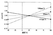
図7は、電界効果トランジスタM3のW/Lが50/10、50/30及び50/50のときの基準電圧Vrefの温度特性を示している。なお、図7では、電界効果トランジスタM2のW/Lは50/10である場合を例にして示している。
図7において、実線で示した電界効果トランジスタM3のW/Lが50/10のときは、基準電圧Vrefの温度特性は−517ppm/℃であり、点線で示した電界効果トランジスタM3のW/Lが50/30のときの基準電圧Vrefの温度特性は585ppm/℃であり、1点鎖線で示した電界効果トランジスタM3のW/Lが50/50のときの基準電圧Vrefの温度特性は1308ppm/℃である。
FIG. 7 shows the temperature characteristics of the reference voltage Vref when the W / L of the field effect transistor M3 is 50/10, 50/30, and 50/50. FIG. 7 shows an example in which the W / L of the field effect transistor M2 is 50/10.
In FIG. 7, when the W / L of the field effect transistor M3 indicated by the solid line is 50/10, the temperature characteristic of the reference voltage Vref is −517 ppm / ° C., and the W / L of the field effect transistor M3 indicated by the dotted line is Is 50/30, the temperature characteristic of the reference voltage Vref is 585 ppm / ° C., and the temperature characteristic of the reference voltage Vref when the W / L of the field effect transistor M3 indicated by the one-dot chain line is 50/50 is 1308 ppm / ° C.
基準電圧Vrefが負の温度特性を持つ場合は、電界効果トランジスタM2及びM3は、電流idMよりもZTC点でのドレイン電流が共に大きいことから、電流idMにおけるゲート‐ソース間電圧Vgsの温度特性はいずれも負である。但し、ZTC点でのドレイン電流はn型電界効果トランジスタM2よりも電界効果トランジスタM3の方が大きいことから、電界効果トランジスタM3のVgs‐id特性はより大きい負の温度特性を持つため、同じく負の温度特性を持つn型トランジスタM2のVgs‐id特性の温度特性をキャンセルしすぎてしまい、結局基準電圧Vrefは負の温度特性を有することになる。 When the reference voltage Vref has a negative temperature characteristic, the field effect transistors M2 and M3 have a larger drain current at the ZTC point than the current idM. Therefore, the temperature characteristic of the gate-source voltage Vgs at the current idM is Both are negative. However, since the drain current at the ZTC point is larger in the field effect transistor M3 than in the n-type field effect transistor M2, the Vgs-id characteristic of the field effect transistor M3 has a larger negative temperature characteristic. The temperature characteristic of the Vgs-id characteristic of the n-type transistor M2 having the above temperature characteristic is canceled too much, and the reference voltage Vref eventually has a negative temperature characteristic.
また、基準電圧Vrefが正の温度特性を持つ場合は、電界効果トランジスタM2は、電流idMよりもZTC点でのドレイン電流が大きいことから、電流idMにおけるゲート‐ソース間電圧Vgsの温度特性は負である。一方、電界効果トランジスタM3は、電流idMよりもZTC点でのドレイン電流が小さいため、電流idMにおけるゲート‐ソース間電圧Vgsの温度特性は正である。これらのことから、基準電圧Vrefは正の温度特性を持ち、したがって、基準電圧Vrefの温度特性を最小にするには、電界効果トランジスタM3は、電界効果トランジスタM2と同程度の負の温度特性を持つ必要がある。実験結果から、基準電圧Vrefの温度特性の最小点は、電界効果トランジスタM3のW/Lが50/18のときであり、約40ppm/℃であることが分かった。 When the reference voltage Vref has a positive temperature characteristic, the field effect transistor M2 has a larger drain current at the ZTC point than the current idM. Therefore, the temperature characteristic of the gate-source voltage Vgs at the current idM is negative. It is. On the other hand, since the field effect transistor M3 has a drain current at the ZTC point smaller than the current idM, the temperature characteristic of the gate-source voltage Vgs at the current idM is positive. Therefore, the reference voltage Vref has a positive temperature characteristic. Therefore, in order to minimize the temperature characteristic of the reference voltage Vref, the field effect transistor M3 has the same negative temperature characteristic as the field effect transistor M2. It is necessary to have. From the experimental results, it was found that the minimum point of the temperature characteristic of the reference voltage Vref is when the W / L of the field effect transistor M3 is 50/18, which is about 40 ppm / ° C.
ここで、NMOSトランジスタM2及びM3の各トランジスタサイズを変えて基準電圧Vrefの温度特性の最小点を探す実験を行っている途中で、図8で示すような現象が発生した。
図8は、電界効果トランジスタM2のW/Lが50/5であり、電界効果トランジスタM3のW/Lが50/10であるときの基準電圧Vrefの温度特性を示した図である。
図8から分かるように、基準電圧Vrefは、図7で示したような正の温度特性又は負の温度特性のみを持つのではなく、低温側では正の温度特性を持ち、高温側では負の温度特性を持っており、特に高温側で温度特性が大きくなっている。
Here, a phenomenon as shown in FIG. 8 occurred during an experiment for searching for the minimum point of the temperature characteristic of the reference voltage Vref by changing the transistor sizes of the NMOS transistors M2 and M3.
FIG. 8 is a graph showing the temperature characteristics of the reference voltage Vref when the W / L of the field effect transistor M2 is 50/5 and the W / L of the field effect transistor M3 is 50/10.
As can be seen from FIG. 8, the reference voltage Vref does not have only a positive temperature characteristic or a negative temperature characteristic as shown in FIG. 7, but has a positive temperature characteristic on the low temperature side and a negative temperature characteristic on the high temperature side. It has temperature characteristics, especially on the high temperature side.
図9は、電界効果トランジスタM2における、ゲート‐ソース間電圧Vgsが0V近辺のときのVgs‐id特性を示した図である。
本来、電界効果トランジスタM2のトランジスタサイズでは、動作点の電流idMよりもZTC点でのドレイン電流の方が大きい。このため、ドレイン電流idが同じであるならばゲート‐ソース間電圧Vgsは負の温度特性を示すはずであり、言い換えればゲート‐ソース間電圧Vgsが同じであるならば、ドレイン電流idは正の温度特性を示すはずである。
しかし、図10に示すように、電界効果トランジスタM2において、ゲート‐ソース間電圧Vgsが0V時のドレイン電流idの温度特性は、上に凸の形状をなしており、一律に正の温度特性にはならない。このため、各温度での電界効果トランジスタM3の動作点は、図11のa〜g点で示したようになり、最終的に基準電圧Vrefは図8のような温度特性を有してしまうことが分かった。
FIG. 9 is a diagram showing Vgs-id characteristics when the gate-source voltage Vgs is around 0 V in the field effect transistor M2.
Originally, in the transistor size of the field effect transistor M2, the drain current at the ZTC point is larger than the current idM at the operating point. Therefore, if the drain current id is the same, the gate-source voltage Vgs should exhibit a negative temperature characteristic. In other words, if the gate-source voltage Vgs is the same, the drain current id is positive. Should show temperature characteristics.
However, as shown in FIG. 10, in the field effect transistor M2, the temperature characteristic of the drain current id when the gate-source voltage Vgs is 0V has an upwardly convex shape, which is uniformly positive. Must not. For this reason, the operating point of the field effect transistor M3 at each temperature is as shown by points a to g in FIG. 11, and the reference voltage Vref finally has temperature characteristics as shown in FIG. I understood.
図5や図6で示すように1点で交わったZTC点であれば、ゲート‐ソース間電圧Vgsの温度特性が負である領域1とゲート‐ソース間電圧Vgsの温度特性が正である領域2の2つの領域に分けることができる。しかし、ZTC点は厳密には1点で交わっておらず、ゲート‐ソース間電圧Vgsの温度特性が正の場合と負の場合が混在する、いわばZTC領域と言うべき領域3が存在する。
電界効果トランジスタM2のZTC点付近を拡大すると図12のようになる。図12で示すように、ゲート‐ソース間電圧Vgsが0Vのときが前記ZTC領域である領域3に存在すると、ドレイン電流idの温度特性は図10のようになり、結局基準電圧Vrefは図8のようになって高温側で温度特性を悪化させてしまう。したがって、このような現象を発生させないためには、図1の基準電圧回路1の動作点をZTC領域である領域3以外の領域にする必要がある。
As shown in FIG. 5 and FIG. 6, if the ZTC point intersects at one point, the
When the vicinity of the ZTC point of the field effect transistor M2 is enlarged, it becomes as shown in FIG. As shown in FIG. 12, when the gate-source voltage Vgs is 0V and exists in the
以上のように、回路の動作点をZTC領域である領域3以外に設定した上で、電界効果トランジスタM2及びM3のサイズ調整をすることにより、基準電圧Vrefの温度特性を約40ppm/℃にすることができ、従来よりも小さくすることができる。但し、この場合、前記(1)式の導電係数が残るため、基準電圧Vrefのばらつきは±5〜6%程度に大きくなるが、従来よりも基準電圧Vrefのばらつきを小さくすることができる。
As described above, the temperature characteristic of the reference voltage Vref is set to about 40 ppm / ° C. by adjusting the size of the field effect transistors M2 and M3 after setting the operating point of the circuit to a region other than the
次に、図13は、電界効果トランジスタM1のソース電圧Vsとソース電流isとの関係を示したVs‐is特性の例を示した図である。
図13では、電源電圧VCCの電圧をVA、VB、VCと変化させ、電界効果トランジスタM1において、ソース電圧Vsを上昇させたときに流れるソース電流isを示している。例えば、電源電圧VCCがVAのときは、ソース電圧VsがVAに近づくとソース電流isが急激に減少し、Vs=VAでソース電流isは0になる。図2で示したように、定電流源をなす電界効果トランジスタM2にはid2のドレイン電流が流れ、同じ電流パス上にある電界効果トランジスタM1にも同じid2の電流が流れる。
Next, FIG. 13 is a diagram illustrating an example of the Vs-is characteristic indicating the relationship between the source voltage Vs and the source current is of the field effect transistor M1.
FIG. 13 shows the source current is that flows when the voltage of the power supply voltage VCC is changed to VA, VB, and VC and the source voltage Vs is increased in the field effect transistor M1. For example, when the power supply voltage VCC is VA, the source current is rapidly decreases when the source voltage Vs approaches VA, and the source current is becomes 0 when Vs = VA. As shown in FIG. 2, the drain current of id2 flows through the field effect transistor M2 forming the constant current source, and the current of id2 also flows through the field effect transistor M1 on the same current path.
したがって、電界効果トランジスタM1のソース電圧Vsは、電源電圧VCCに関係なくVCC2に固定される。但し、id2が小さすぎて、id2aになったときの電界効果トランジスタM1のソース電圧Vsの値はVCC2aになることから、VCC=VB又はVCC=VCのときは、VCC2a<VB、VCC2a<VCであり、電界効果トランジスタM1のソース電圧VsはVCC2aに固定される。しかし、VCC=VAのときは、VCC2a>VAであることから、電界効果トランジスタM1のソース電圧VsはVAにしかならない。したがって、回路の最低動作電圧によって、必要な電流id2、又はVCC2を設定しなければならないが、これは電界効果トランジスタM1のゲート幅W/ゲート長Lを調整することで、簡単に得ることができる。 Therefore, the source voltage Vs of the field effect transistor M1 is fixed to VCC2 regardless of the power supply voltage VCC. However, since the value of the source voltage Vs of the field effect transistor M1 when id2 is too small and becomes id2a is VCC2a, when VCC = VB or VCC = VC, VCC2a <VB and VCC2a <VC. Yes, the source voltage Vs of the field effect transistor M1 is fixed to VCC2a. However, when VCC = VA, since VCC2a> VA, the source voltage Vs of the field effect transistor M1 is only VA. Therefore, the necessary current id2 or VCC2 must be set according to the minimum operating voltage of the circuit, but this can be easily obtained by adjusting the gate width W / gate length L of the field effect transistor M1. .
以上のように、電界効果トランジスタM1を設けることにより、電界効果トランジスタM2及びM3の各ソース‐ドレイン間電圧VdsM2及びVdsM3は、
VdsM2=VCC2−Vref
VdsM3=Vref
となるため、電源電圧VCCが変動しても、電界効果トランジスタM2及びM3の各ソース‐ドレイン間電圧はそれぞれ影響を受けなくなり、基準電圧Vrefの変動が起こらない。
図14は、電界効果トランジスタM1がある場合とない場合における、基準電圧Vrefの電源電圧依存性を示した実験データである。
図14から分かるように、電界効果トランジスタM1がある場合の基準電圧Vrefの電圧変動は、電界効果トランジスタM1がない場合の1/10以下である0.4mVである。このように、電界効果トランジスタM1を設けることにより、電源電圧VCCの変動に対する基準電圧Vrefの変動を減少させることができる。
As described above, by providing the field effect transistor M1, the source-drain voltages VdsM2 and VdsM3 of the field effect transistors M2 and M3 are
VdsM2 = VCC2-Vref
VdsM3 = Vref
Therefore, even if the power supply voltage VCC varies, the source-drain voltages of the field effect transistors M2 and M3 are not affected and the reference voltage Vref does not vary.
FIG. 14 is experimental data showing the power supply voltage dependence of the reference voltage Vref with and without the field effect transistor M1.
As can be seen from FIG. 14, the voltage fluctuation of the reference voltage Vref in the presence of the field effect transistor M1 is 0.4 mV, which is 1/10 or less of that in the absence of the field effect transistor M1. As described above, by providing the field effect transistor M1, it is possible to reduce the fluctuation of the reference voltage Vref with respect to the fluctuation of the power supply voltage VCC.
ここで、図15は、前記基準電圧発生回路1を使用した定電圧回路の例を示した図であり、図15では、シリーズレギュレータに使用した場合を例にして示している。
図15において、シリーズレギュレータ10は、所定の基準電圧Vrefを生成して出力する基準電圧発生回路1と、誤差増幅回路A11と、PMOSトランジスタからなる出力トランジスタM11と、出力電圧検出用の抵抗R11,R12とで構成されている。
入力端子INと出力端子OUTとの間に出力トランジスタM11が接続され、出力端子OUTと接地電圧GNDとの間に抵抗R11及びR12が直列に接続されている。抵抗R11及びR12は、出力電圧Voutを分圧して分圧電圧Vfbを生成し、誤差増幅回路A11の非反転入力端に出力する。誤差増幅回路A11の反転入力端には基準電圧Vrefが入力され、誤差増幅回路A11は、分圧電圧Vfbが基準電圧Vrefになるように出力トランジスタM11の動作制御を行う。また、出力端子OUTと接地電圧GNDとの間には、負荷11が接続されている。
Here, FIG. 15 is a diagram showing an example of a constant voltage circuit using the reference
In FIG. 15, a
An output transistor M11 is connected between the input terminal IN and the output terminal OUT, and resistors R11 and R12 are connected in series between the output terminal OUT and the ground voltage GND. The resistors R11 and R12 divide the output voltage Vout to generate a divided voltage Vfb, which is output to the non-inverting input terminal of the error amplifier circuit A11. The reference voltage Vref is input to the inverting input terminal of the error amplifier circuit A11, and the error amplifier circuit A11 controls the operation of the output transistor M11 so that the divided voltage Vfb becomes the reference voltage Vref. A
また、図16は、前記基準電圧発生回路1を使用した定電圧回路の他の例を示した図であり、図16では、スイッチングレギュレータに使用した場合を例にして示している。
図16において、スイッチングレギュレータ20は、入力電圧Vinの出力制御を行うためのスイッチング動作を行うPMOSトランジスタからなる第1のスイッチング素子M21と、NMOSトランジスタからなる同期整流用のスイッチング素子M22と、平滑回路を構成するインダクタL1及びコンデンサC1と、出力電圧Voを分圧して分圧電圧VFBを生成し出力する出力電圧検出用の抵抗R21,R22とを備えている。
FIG. 16 is a diagram showing another example of a constant voltage circuit using the reference
In FIG. 16, a switching
また、スイッチングレギュレータ20は、所定の基準電圧Vrefを生成して出力する基準電圧発生回路1と、前記分圧電圧VFBと該基準電圧Vrefとの電圧比較を行い、該比較結果に応じた電圧の出力信号Errを出力する誤差増幅回路21と、該誤差増幅回路21の出力信号Errに応じて第1のスイッチング素子M21及び同期整流用のスイッチング素子M22に対してPWM制御を行って第1のスイッチング素子M21及び同期整流用のスイッチング素子M22のスイッチング制御を行うPWM制御回路22と、所定の周波数の三角波信号TWを生成してPWM制御回路22に出力する発振回路OSCとを備えている。
一方、PWM制御回路22は、誤差増幅回路21の出力信号Errと発振回路OSCからの三角波信号TWからPWM制御を行うためのパルス信号Spwを生成して出力するPWM回路25と、該PWM回路25からのパルス信号Spwに応じて、第1のスイッチング素子M21のスイッチング制御を行うための制御信号PDと同期整流用のスイッチング素子M22のスイッチング制御を行うための制御信号NDをそれぞれ生成して駆動するドライブ回路26とを備えている。
The switching
On the other hand, the
出力端子OUTと接地電圧との間には負荷30が接続されている。入力端子INと出力端子OUTとの間には、第1のスイッチング素子M21とインダクタL1が直列に接続されている。また、第1のスイッチング素子M21とインダクタL1との接続部と接地電圧との間に同期整流用のスイッチング素子M22が接続され、出力端子OUTと接地電圧との間にはコンデンサC1が接続されている。出力端子OUTと接地電圧との間に抵抗R21と抵抗R22の直列回路が接続されている。
A
抵抗R21と抵抗R22との接続部は、誤差増幅回路21の反転入力端に接続され、誤差増幅回路21の非反転入力端には基準電圧Vrefが入力されている。誤差増幅回路21の出力信号Errは、PWM回路25をなすコンパレータの反転入力端に出力され、発振回路OSCからの三角波信号TWは、PWM回路11をなすコンパレータの非反転入力端に出力される。PWM回路25からのパルス信号Spwはドライブ回路26に出力される。ドライブ回路26は、第1のスイッチング素子M21のスイッチング制御を行うための制御信号PDを第1のスイッチング素子M21のゲートに出力し、同期整流用のスイッチング素子M22のスイッチング制御を行うための制御信号NDを同期整流用のスイッチング素子M22のゲートに出力する。
A connection portion between the resistor R21 and the resistor R22 is connected to an inverting input terminal of the
このような構成において、スイッチングレギュレータ20は、同期整流方式のスイッチングレギュレータとして作動し、第1のスイッチング素子M21はスイッチング動作を行う。第1のスイッチング素子M21がオンしたときに、インダクタL1に電流が供給され、このとき、同期整流用のスイッチング素子M22はオフしている。第1のスイッチング素子M21がオフすると、同期整流用のスイッチング素子M22がオンし、インダクタL1に蓄えられていたエネルギーが同期整流用のスイッチング素子M22を通して放出される。このとき発生した電流は、コンデンサC1で平滑されて出力端子OUTから負荷30に出力される。
In such a configuration, the switching
また、出力端子OUTから出力される出力電圧Voは、出力電圧検出用の抵抗R21とR22で分圧され、該分圧電圧VFBが誤差増幅回路21の反転入力端に入力される。誤差増幅回路21の非反転入力端には基準電圧Vrefが入力されていることから、分圧電圧VFBと基準電圧Vrefとの電圧差が誤差増幅回路21で増幅されてPWM回路25の反転入力端に出力される。PWM回路25の非反転入力端には、発振回路OSCからの三角波信号TWが入力され、PWM回路25は、PWM制御されたパルス信号Spwをドライブ回路26に出力する。
The output voltage Vo output from the output terminal OUT is divided by the output voltage detection resistors R21 and R22, and the divided voltage VFB is input to the inverting input terminal of the
スイッチングレギュレータ20の出力電圧Voが大きくなると、誤差増幅回路21の出力信号Errの電圧が低下し、PWM回路25のパルス信号Spwのデューティサイクルは小さくなる。その結果、第1のスイッチング素子M21がオンする時間が短くなり、スイッチングレギュレータ20の出力電圧Voが低下するように制御される。スイッチングレギュレータ20の出力電圧Voが小さくなると、前記と逆の動作を行い、結果としてスイッチングレギュレータ20の出力電圧Voが一定になるように制御される。
When the output voltage Vo of the switching
前記のように、本第1の実施の形態における基準電圧発生回路は、従来回路に対して、初期精度は±30%から±6%に、温度特性は300ppm/℃から40ppm/℃にそれぞれ改善され、更に電源電圧変動に対する基準電圧Vrefの変動を1/10以下に低減させることができる。 As described above, the reference voltage generation circuit according to the first embodiment has an initial accuracy improved from ± 30% to ± 6% and a temperature characteristic from 300 ppm / ° C. to 40 ppm / ° C. with respect to the conventional circuit. Further, the fluctuation of the reference voltage Vref with respect to the fluctuation of the power supply voltage can be reduced to 1/10 or less.
第2の実施の形態.
前記第1の実施の形態では、電界効果トランジスタM2のサブストレートゲートは、電界効果トランジスタM2のソースに接続されていたが、電界効果トランジスタM2のサブストレートゲートを接地電圧GNDに接続するようにしてもよく、このようにしたものを本発明の第2の実施の形態とする。
図17は、本発明の第2の実施の形態における基準電圧発生回路の例を示した回路図である。なお、図17では、図1と同じものは同じ符号で示し、ここではその説明を省略すると共に図1との相違点のみ説明する。
図17における図1との相違点は、電界効果トランジスタM2のサブストレートゲートを接地電圧GNDに接続したことにある。
Second embodiment.
In the first embodiment, the substrate gate of the field effect transistor M2 is connected to the source of the field effect transistor M2. However, the substrate gate of the field effect transistor M2 is connected to the ground voltage GND. This is what is described as a second embodiment of the present invention.
FIG. 17 is a circuit diagram showing an example of a reference voltage generation circuit according to the second embodiment of the present invention. In FIG. 17, the same components as those in FIG. 1 are denoted by the same reference numerals, and description thereof is omitted here, and only differences from FIG. 1 are described.
17 differs from FIG. 1 in that the substrate gate of the field effect transistor M2 is connected to the ground voltage GND.
このような構成において、前記図1と同様、プロセスの変動によって、基板やチャネルドープの不純物濃度がばらついても、電界効果トランジスタM2とM3の該各濃度は同様にばらつく。このため、図3に示すように、電界効果トランジスタM2とM3の各Vgs‐id特性は、図2の関係を保ったまま、左右に移動するだけであり、基準電圧Vrefの絶対値にはほとんど影響を与えず安定した基準電圧Vrefを発生させることができる。
また、電界効果トランジスタM2に基板バイアス効果が発生するため、前記第1の実施の形態と比較して、チャネル領域のポテンシャル差が若干温度特性を持つようになるが、従来よりも温度特性は小さい。
In such a configuration, the respective concentrations of the field effect transistors M2 and M3 similarly vary even if the impurity concentration of the substrate and the channel dope varies due to process variations, as in FIG. Therefore, as shown in FIG. 3, the Vgs-id characteristics of the field effect transistors M2 and M3 only move to the left and right while maintaining the relationship of FIG. 2, and the absolute value of the reference voltage Vref is almost the same. A stable reference voltage Vref can be generated without any influence.
Further, since the substrate bias effect is generated in the field effect transistor M2, the potential difference in the channel region has a slight temperature characteristic as compared with the first embodiment, but the temperature characteristic is smaller than the conventional one. .
そこで、前記第1の実施の形態と同様に、電界効果トランジスタM2及びM3のドレイン電流がidMのときの温度特性を正又は負になるように、電界効果トランジスタM2及びM3のサイズ調整をすることにより、基準電圧Vrefの温度特性を約40ppm/℃にすることができ、従来よりも基準電圧Vrefの温度特性を小さくすることができる。
具体的には、図18は、S3/S2の比に対する基準電圧Vrefの温度特性の実験データを示した図である。図18から、S3/S2の比が0.35〜0.45の間に温度特性の最小点があることが分かる。該最小点になる最適の比S3/S2を推定すると、0.37〜0.41であり、このときの温度特性は、約40ppm/℃になることが分かった。このように、S3/S2の値を変えることにより基準電圧Vrefの温度特性を小さくすることができる。
Therefore, as in the first embodiment, the size of the field effect transistors M2 and M3 is adjusted so that the temperature characteristics when the drain currents of the field effect transistors M2 and M3 are idM are positive or negative. As a result, the temperature characteristic of the reference voltage Vref can be set to about 40 ppm / ° C., and the temperature characteristic of the reference voltage Vref can be made smaller than in the past.
Specifically, FIG. 18 is a diagram illustrating experimental data of temperature characteristics of the reference voltage Vref with respect to the ratio of S3 / S2. From FIG. 18, it can be seen that there is a minimum point of the temperature characteristic when the ratio of S3 / S2 is between 0.35 and 0.45. The optimum ratio S3 / S2 that would be the minimum point was estimated to be 0.37 to 0.41, and the temperature characteristic at this time was found to be about 40 ppm / ° C. Thus, the temperature characteristic of the reference voltage Vref can be reduced by changing the value of S3 / S2.
また、前記第1の実施の形態と同様、電界効果トランジスタM2とM3のソース‐ドレイン間電圧VdsM2及びVdsM3は、
VdsM2=Vcc2−Vref
VdsM3=Vref
となるため、電源電圧VCCが変動しても、電界効果トランジスタM2及びM3のソース‐ドレイン間電圧はそれぞれ影響を受けなくなり、基準電圧Vrefの変動が起こらない。
As in the first embodiment, the source-drain voltages VdsM2 and VdsM3 of the field effect transistors M2 and M3 are
VdsM2 = Vcc2-Vref
VdsM3 = Vref
Therefore, even if the power supply voltage VCC changes, the source-drain voltages of the field effect transistors M2 and M3 are not affected, and the reference voltage Vref does not change.
このように、本第2の実施の形態の基準電圧発生回路は、前記第1の実施の形態と同様の効果を得ることができると共に、例えば、p型基板中に電界効果トランジスタM1〜M3を構成する場合等、電界効果トランジスタM2の基板電圧が接地電圧GNDに固定されてしまう場合に使用できる。更に、電界効果トランジスタM1〜M3の基板電圧がすべて接地電圧GNDであることから、電界効果トランジスタ間にスペースを設ける必要がなく、チップ面積を縮小させることができる。 As described above, the reference voltage generation circuit according to the second embodiment can obtain the same effects as those of the first embodiment. For example, the field effect transistors M1 to M3 are provided in a p-type substrate. This can be used when the substrate voltage of the field effect transistor M2 is fixed to the ground voltage GND, such as when configured. Furthermore, since all the substrate voltages of the field effect transistors M1 to M3 are the ground voltage GND, it is not necessary to provide a space between the field effect transistors, and the chip area can be reduced.
なお、ノイズ特性等、ケースバイケースで前記第1の実施の形態又は第2の実施の形態を選択すればよい。また、前記第1の実施の形態と同様に、前記第2の実施の形態の基準電圧発生回路を図15及び図16で示したような定電圧回路に使用することができる。 In addition, what is necessary is just to select the said 1st Embodiment or 2nd Embodiment on a case-by-case basis, such as a noise characteristic. Similarly to the first embodiment, the reference voltage generation circuit of the second embodiment can be used for the constant voltage circuit as shown in FIGS.
1 基準電圧発生回路
M1〜M3 電界効果トランジスタ
10 シリーズレギュレータ
A1,21 誤差増幅回路
M10 出力トランジスタ
R1,R2,R21,R22 抵抗
20 スイッチングレギュレータ
M21 第1のスイッチング素子
M22 同期整流用のスイッチング素子
L1 インダクタ
C1 コンデンサ
22 PWM制御回路
25 PWM回路
26 ドライブ回路
OSC 発振回路
DESCRIPTION OF
Claims (16)
一端が所定の電源電圧に接続された、デプレッション型のnチャネル型電界効果トランジスタである第1の電界効果トランジスタと、
一端が該第1の電界効果トランジスタの他端に接続された、高濃度n型ゲートを有する第2の電界効果トランジスタと、
一端が該第2の電界効果トランジスタの他端に接続され、他端が接地電圧に接続された、高濃度p型ゲートを有する第3の電界効果トランジスタと、
を備え、
前記第1の電界効果トランジスタのゲートは、該第1の電界効果トランジスタと前記第2の電界効果トランジスタとの接続部に接続されると共に、前記第1及び第3の各電界効果トランジスタのサブストレートゲートは、それぞれ接地電圧に接続され、前記第2の電界効果トランジスタのゲート及びサブストレートゲート、並びに前記第3の電界効果トランジスタのゲートは、前記出力端をなす第2及び第3の各電界効果トランジスタの接続部にそれぞれ接続され、前記第2及び第3の各電界効果トランジスタは、ゲート‐ソース間電圧が正又は負の同一極性の温度特性を有するように、ゲート‐ソース間電圧とドレイン電流との関係が設定されると共に、前記基準電圧の温度特性の絶対値が低下するようなチャネル幅とチャネル長との比にそれぞれ形成されることを特徴とする基準電圧発生回路。 In a reference voltage generation circuit that generates a predetermined reference voltage and outputs it from the output terminal,
A first field effect transistor that is a depletion type n-channel field effect transistor, one end of which is connected to a predetermined power supply voltage;
A second field effect transistor having a high concentration n-type gate, one end connected to the other end of the first field effect transistor;
A third field effect transistor having a high-concentration p-type gate having one end connected to the other end of the second field effect transistor and the other end connected to a ground voltage;
With
A gate of the first field effect transistor is connected to a connection portion between the first field effect transistor and the second field effect transistor, and a substrate of each of the first and third field effect transistors. The gates are respectively connected to a ground voltage, and the gates and the substrate gates of the second field effect transistors and the gates of the third field effect transistors are the second and third field effects forming the output terminal, respectively. Each of the second and third field effect transistors is connected to a connection portion of the transistor, and the gate-source voltage and the drain current are set such that the gate-source voltage has a temperature characteristic of the same polarity of positive or negative. with relationship is set between, on the ratio between the channel width and channel length as the absolute value decreases the temperature characteristics of the reference voltage Reference voltage generating circuit, characterized in that the respectively formed.
一端が所定の電源電圧に接続された、デプレッション型のnチャネル型電界効果トランジスタである第1の電界効果トランジスタと、
一端が該第1の電界効果トランジスタの他端に接続された、高濃度n型ゲートを有する第2の電界効果トランジスタと、
一端が該第2の電界効果トランジスタの他端に接続され、他端が接地電圧に接続された、高濃度p型ゲートを有する第3の電界効果トランジスタと、
を備え、
前記第1の電界効果トランジスタのゲートは、該第1の電界効果トランジスタと前記第2の電界効果トランジスタとの接続部に接続されると共に、前記第1から第3の各電界効果トランジスタのサブストレートゲートは、それぞれ接地電圧に接続され、前記第2及び第3の各電界効果トランジスタのゲートは、前記出力端をなす前記第2及び第3の各電界効果トランジスタの接続部にそれぞれ接続され、前記第2及び第3の各電界効果トランジスタは、ゲート‐ソース間電圧が正又は負の同一極性の温度特性を有するように、ゲート‐ソース間電圧とドレイン電流との関係が設定されると共に、前記基準電圧の温度特性の絶対値が低下するようなチャネル幅とチャネル長との比にそれぞれ形成されることを特徴とする基準電圧発生回路。 In a reference voltage generation circuit that generates a predetermined reference voltage and outputs it from the output terminal,
A first field effect transistor that is a depletion type n-channel field effect transistor, one end of which is connected to a predetermined power supply voltage;
A second field effect transistor having a high concentration n-type gate, one end connected to the other end of the first field effect transistor;
A third field effect transistor having a high-concentration p-type gate having one end connected to the other end of the second field effect transistor and the other end connected to a ground voltage;
With
A gate of the first field effect transistor is connected to a connection portion between the first field effect transistor and the second field effect transistor, and a substrate of each of the first to third field effect transistors. The gates are respectively connected to a ground voltage, and the gates of the second and third field effect transistors are respectively connected to connection portions of the second and third field effect transistors forming the output terminal, In each of the second and third field effect transistors, the relationship between the gate-source voltage and the drain current is set so that the gate-source voltage has a positive or negative temperature characteristic of the same polarity. A reference voltage generation circuit, characterized in that it is formed in a ratio of channel width and channel length such that the absolute value of the temperature characteristic of the reference voltage decreases .
前記基準電圧発生回路は、
一端が所定の電源電圧に接続された、デプレッション型のnチャネル型電界効果トランジスタである第1の電界効果トランジスタと、
一端が該第1の電界効果トランジスタの他端に接続された、高濃度n型ゲートを有する第2の電界効果トランジスタと、
一端が該第2の電界効果トランジスタの他端に接続され、他端が接地電圧に接続された、高濃度p型ゲートを有する第3の電界効果トランジスタと、
を備え、
前記第1の電界効果トランジスタのゲートは、該第1の電界効果トランジスタと前記第2の電界効果トランジスタとの接続部に接続されると共に、前記第1及び第3の各電界効果トランジスタのサブストレートゲートは、それぞれ接地電圧に接続され、前記第2の電界効果トランジスタのゲート及びサブストレートゲート、並びに前記第3の電界効果トランジスタのゲートは、前記基準電圧を出力する出力端をなす前記第2及び第3の各電界効果トランジスタの接続部にそれぞれ接続され、前記第2及び第3の各電界効果トランジスタは、ゲート‐ソース間電圧が正又は負の同一極性の温度特性を有するように、ゲート‐ソース間電圧とドレイン電流との関係が設定されると共に、前記基準電圧の温度特性の絶対値が低下するようなチャネル幅とチャネル長との比にそれぞれ形成されることを特徴とする定電圧回路。 In a constant voltage circuit that generates and outputs a predetermined constant voltage from an input voltage with reference to a predetermined reference voltage generated by a reference voltage generation circuit,
The reference voltage generation circuit includes:
A first field effect transistor that is a depletion type n-channel field effect transistor, one end of which is connected to a predetermined power supply voltage;
A second field effect transistor having a high concentration n-type gate, one end connected to the other end of the first field effect transistor;
A third field effect transistor having a high-concentration p-type gate having one end connected to the other end of the second field effect transistor and the other end connected to a ground voltage;
With
A gate of the first field effect transistor is connected to a connection portion between the first field effect transistor and the second field effect transistor, and a substrate of each of the first and third field effect transistors. The gates are respectively connected to a ground voltage, and the gates and the substrate gates of the second field effect transistors and the gates of the third field effect transistors form the output terminals for outputting the reference voltage. Each of the second and third field effect transistors is connected to a connection portion of each third field effect transistor, and the second and third field effect transistors have a gate-source voltage having a temperature characteristic of the same polarity of positive or negative. A channel in which the relationship between the source voltage and the drain current is set and the absolute value of the temperature characteristic of the reference voltage is reduced. Constant voltage circuit being formed respectively to the ratio of the channel length.
前記基準電圧発生回路は、
一端が所定の電源電圧に接続された、デプレッション型のnチャネル型電界効果トランジスタである第1の電界効果トランジスタと、
一端が該第1の電界効果トランジスタの他端に接続された、高濃度n型ゲートを有する第2の電界効果トランジスタと、
一端が該第2の電界効果トランジスタの他端に接続され、他端が接地電圧に接続された、高濃度p型ゲートを有する第3の電界効果トランジスタと、
を備え、
前記第1の電界効果トランジスタのゲートは、該第1の電界効果トランジスタと前記第2の電界効果トランジスタとの接続部に接続されると共に、前記第1から第3の各電界効果トランジスタのサブストレートゲートは、それぞれ接地電圧に接続され、前記第2及び第3の各電界効果トランジスタのゲートは、前記基準電圧を出力する出力端をなす前記第2及び第3の各電界効果トランジスタの接続部にそれぞれ接続され、前記第2及び第3の各電界効果トランジスタは、ゲート‐ソース間電圧が正又は負の同一極性の温度特性を有するように、ゲート‐ソース間電圧とドレイン電流との関係が設定されると共に、前記基準電圧の温度特性の絶対値が低下するようなチャネル幅とチャネル長との比にそれぞれ形成されることを特徴とする定電圧回路。 In a constant voltage circuit that generates and outputs a predetermined constant voltage from an input voltage with reference to a predetermined reference voltage generated by a reference voltage generation circuit,
The reference voltage generation circuit includes:
A first field effect transistor that is a depletion type n-channel field effect transistor, one end of which is connected to a predetermined power supply voltage;
A second field effect transistor having a high concentration n-type gate, one end connected to the other end of the first field effect transistor;
A third field effect transistor having a high-concentration p-type gate having one end connected to the other end of the second field effect transistor and the other end connected to a ground voltage;
With
A gate of the first field effect transistor is connected to a connection portion between the first field effect transistor and the second field effect transistor, and a substrate of each of the first to third field effect transistors. Gates are respectively connected to a ground voltage, and gates of the second and third field effect transistors are connected to connection portions of the second and third field effect transistors that form an output terminal for outputting the reference voltage. Each of the second and third field effect transistors is connected, and the relationship between the gate-source voltage and the drain current is set so that the gate-source voltage has the same polarity of positive or negative temperature characteristics. with the absolute value of the temperature characteristic of the reference voltage is being formed respectively on the ratio between the channel width and channel length as to decrease constant- Circuit.
Each of the second and third field effect transistors is formed such that a ratio S3 / S2 of a ratio S3 to S2 of a channel width to a channel length is 0.37 to 0.41. The constant voltage circuit according to claim 15.
Priority Applications (3)
| Application Number | Priority Date | Filing Date | Title |
|---|---|---|---|
| JP2005252011A JP4713280B2 (en) | 2005-08-31 | 2005-08-31 | Reference voltage generation circuit and constant voltage circuit using the reference voltage generation circuit |
| US11/506,029 US7426146B2 (en) | 2005-08-31 | 2006-08-16 | Reference voltage generating circuit and constant voltage circuit |
| US12/187,899 US7843253B2 (en) | 2005-08-31 | 2008-08-07 | Reference voltage generating circuit and constant voltage circuit |
Applications Claiming Priority (1)
| Application Number | Priority Date | Filing Date | Title |
|---|---|---|---|
| JP2005252011A JP4713280B2 (en) | 2005-08-31 | 2005-08-31 | Reference voltage generation circuit and constant voltage circuit using the reference voltage generation circuit |
Publications (2)
| Publication Number | Publication Date |
|---|---|
| JP2007066046A JP2007066046A (en) | 2007-03-15 |
| JP4713280B2 true JP4713280B2 (en) | 2011-06-29 |
Family
ID=37803860
Family Applications (1)
| Application Number | Title | Priority Date | Filing Date |
|---|---|---|---|
| JP2005252011A Active JP4713280B2 (en) | 2005-08-31 | 2005-08-31 | Reference voltage generation circuit and constant voltage circuit using the reference voltage generation circuit |
Country Status (2)
| Country | Link |
|---|---|
| US (2) | US7426146B2 (en) |
| JP (1) | JP4713280B2 (en) |
Cited By (1)
| Publication number | Priority date | Publication date | Assignee | Title |
|---|---|---|---|---|
| JP2008070953A (en) * | 2006-09-12 | 2008-03-27 | Ricoh Co Ltd | Reference voltage generating circuit |
Families Citing this family (30)
| Publication number | Priority date | Publication date | Assignee | Title |
|---|---|---|---|---|
| JP4704860B2 (en) * | 2005-08-31 | 2011-06-22 | 株式会社リコー | Reference voltage generation circuit and constant voltage circuit using the reference voltage generation circuit |
| JP4713280B2 (en) * | 2005-08-31 | 2011-06-29 | 株式会社リコー | Reference voltage generation circuit and constant voltage circuit using the reference voltage generation circuit |
| US7727833B2 (en) * | 2008-04-07 | 2010-06-01 | Microchip Technology Incorporated | Work function based voltage reference |
| JP5446895B2 (en) | 2010-01-12 | 2014-03-19 | 株式会社リコー | Amplifier |
| JP5470128B2 (en) * | 2010-03-26 | 2014-04-16 | ローム株式会社 | Constant voltage circuit, comparator and voltage monitoring circuit using them |
| JP2011211444A (en) * | 2010-03-29 | 2011-10-20 | Seiko Instruments Inc | Internal power supply voltage generation circuit |
| WO2013125163A1 (en) * | 2012-02-24 | 2013-08-29 | パナソニック株式会社 | Reference voltage source circuit |
| KR102053944B1 (en) | 2013-02-21 | 2019-12-11 | 삼성전자주식회사 | Nonvolatile memory device and memory system including the same |
| US9632521B2 (en) * | 2013-03-13 | 2017-04-25 | Analog Devices Global | Voltage generator, a method of generating a voltage and a power-up reset circuit |
| US9525407B2 (en) | 2013-03-13 | 2016-12-20 | Analog Devices Global | Power monitoring circuit, and a power up reset generator |
| JP6263914B2 (en) | 2013-09-10 | 2018-01-24 | 株式会社リコー | Imaging device, driving method of imaging device, and camera |
| JP6387743B2 (en) | 2013-12-16 | 2018-09-12 | 株式会社リコー | Semiconductor device and manufacturing method of semiconductor device |
| JP6281297B2 (en) | 2014-01-27 | 2018-02-21 | 株式会社リコー | Phototransistor and semiconductor device |
| JP6354221B2 (en) | 2014-03-12 | 2018-07-11 | 株式会社リコー | Imaging apparatus and electronic apparatus |
| JP6340841B2 (en) * | 2014-03-13 | 2018-06-13 | 富士電機株式会社 | Insulated gate device drive circuit |
| JP2016025261A (en) | 2014-07-23 | 2016-02-08 | 株式会社リコー | Imaging device, imaging device control method, and pixel structure |
| JP2016092178A (en) | 2014-11-04 | 2016-05-23 | 株式会社リコー | Solid-state image sensor |
| US10310537B2 (en) * | 2016-06-14 | 2019-06-04 | The Regents Of The University Of Michigan | Variation-tolerant voltage reference |
| US9971373B1 (en) * | 2016-12-28 | 2018-05-15 | AUCMOS Technologies USA, Inc. | Reference voltage generator |
| JP7154102B2 (en) * | 2018-10-24 | 2022-10-17 | エイブリック株式会社 | Reference voltage circuit and power-on reset circuit |
| KR102204130B1 (en) * | 2019-06-11 | 2021-01-18 | 포항공과대학교 산학협력단 | Electronic circuit for generating reference voltage |
| US10782723B1 (en) * | 2019-11-01 | 2020-09-22 | Analog Devices International Unlimited Company | Reference generator using fet devices with different gate work functions |
| CN110879625B (en) * | 2019-12-13 | 2022-02-11 | 东南大学 | A CMOS Voltage Reference Circuit with Ultra-Low Linear Sensitivity |
| EP4033312B1 (en) | 2020-11-25 | 2024-08-21 | Changxin Memory Technologies, Inc. | Control circuit and delay circuit |
| US11681313B2 (en) | 2020-11-25 | 2023-06-20 | Changxin Memory Technologies, Inc. | Voltage generating circuit, inverter, delay circuit, and logic gate circuit |
| EP4033661B1 (en) | 2020-11-25 | 2024-01-24 | Changxin Memory Technologies, Inc. | Control circuit and delay circuit |
| EP4033664B1 (en) * | 2020-11-25 | 2024-01-10 | Changxin Memory Technologies, Inc. | Potential generation circuit, inverter, delay circuit, and logic gate circuit |
| CN112650351B (en) * | 2020-12-21 | 2022-06-24 | 北京中科芯蕊科技有限公司 | Sub-threshold voltage reference circuit |
| CN115220514B (en) * | 2021-04-16 | 2024-08-20 | 中国科学院微电子研究所 | Voltage reference source, chip and electronic equipment |
| CN115373460B (en) * | 2022-09-16 | 2024-05-10 | 昇陌微电子(苏州)有限公司 | Voltage reference source and integrated circuit |
Citations (16)
| Publication number | Priority date | Publication date | Assignee | Title |
|---|---|---|---|---|
| US6005378A (en) * | 1998-03-05 | 1999-12-21 | Impala Linear Corporation | Compact low dropout voltage regulator using enhancement and depletion mode MOS transistors |
| JP2000020153A (en) * | 1998-06-30 | 2000-01-21 | Nec Ic Microcomput Syst Ltd | Constant voltage circuit |
| JP2001159923A (en) * | 1999-12-03 | 2001-06-12 | Fuji Electric Co Ltd | Reference voltage circuit |
| JP2002006968A (en) * | 2000-06-23 | 2002-01-11 | Ricoh Co Ltd | Reference voltage generating circuit and electric power supply unit |
| JP2002091590A (en) * | 2000-09-14 | 2002-03-29 | Ricoh Co Ltd | Reference voltage generation circuit and power supply |
| JP2002140124A (en) * | 2000-10-30 | 2002-05-17 | Seiko Epson Corp | Reference voltage circuit |
| JP2002170886A (en) * | 2000-09-19 | 2002-06-14 | Seiko Instruments Inc | Semiconductor device for reference voltage and method of manufacturing the same |
| JP2002368107A (en) * | 2001-06-07 | 2002-12-20 | Ricoh Co Ltd | Reference voltage generator circuit and power source using the same |
| JP2003031678A (en) * | 2001-07-16 | 2003-01-31 | Fuji Electric Co Ltd | MOS reference voltage circuit and method of manufacturing the same |
| JP2003233429A (en) * | 2002-02-08 | 2003-08-22 | Hitachi Ltd | Power supply circuit and bias circuit |
| JP2003270052A (en) * | 2002-03-20 | 2003-09-25 | Ricoh Co Ltd | Temperature detection circuit |
| JP2005044051A (en) * | 2003-07-25 | 2005-02-17 | Ricoh Co Ltd | Reference voltage generating circuit |
| JP2005071172A (en) * | 2003-08-26 | 2005-03-17 | Ricoh Co Ltd | Reference voltage generation circuit |
| JP2005109364A (en) * | 2003-10-02 | 2005-04-21 | Ricoh Co Ltd | Semiconductor device |
| JP2007066043A (en) * | 2005-08-31 | 2007-03-15 | Ricoh Co Ltd | Reference voltage generation circuit and constant voltage circuit using the reference voltage generation circuit |
| US7426146B2 (en) * | 2005-08-31 | 2008-09-16 | Ricoh Company, Ltd. | Reference voltage generating circuit and constant voltage circuit |
Family Cites Families (13)
| Publication number | Priority date | Publication date | Assignee | Title |
|---|---|---|---|---|
| JPS54132753A (en) * | 1978-04-05 | 1979-10-16 | Hitachi Ltd | Referential voltage generator and its application |
| JPS56108258A (en) * | 1980-02-01 | 1981-08-27 | Seiko Instr & Electronics Ltd | Semiconductor device |
| JPS59200320A (en) * | 1983-04-27 | 1984-11-13 | Hitachi Ltd | Generating circuit of reference voltage |
| JPS6299817A (en) * | 1985-10-25 | 1987-05-09 | Seiko Instr & Electronics Ltd | Constant voltage circuit |
| JPH0465546A (en) | 1990-06-29 | 1992-03-02 | Kawamoto Seiki Kk | Method for displaying sizing pick up of warp and display therefor |
| JPH0772943A (en) * | 1993-09-03 | 1995-03-17 | Toshiba Corp | Constant voltage circuit |
| JPH08123566A (en) * | 1994-08-31 | 1996-05-17 | Mitsubishi Electric Corp | Reference voltage generating circuit and method for manufacturing semiconductor device |
| JPH08184505A (en) * | 1994-11-02 | 1996-07-16 | Seiko Instr Inc | Temperature detector |
| JP4084872B2 (en) * | 1997-08-28 | 2008-04-30 | 株式会社リコー | Voltage regulator |
| JP4194237B2 (en) | 1999-12-28 | 2008-12-10 | 株式会社リコー | Voltage generation circuit and reference voltage source circuit using field effect transistor |
| US6552603B2 (en) * | 2000-06-23 | 2003-04-22 | Ricoh Company Ltd. | Voltage reference generation circuit and power source incorporating such circuit |
| JP2002328732A (en) * | 2001-05-07 | 2002-11-15 | Texas Instr Japan Ltd | Reference voltage generating circuit |
| JP2004318235A (en) * | 2003-04-11 | 2004-11-11 | Renesas Technology Corp | Reference voltage generating circuit |
-
2005
- 2005-08-31 JP JP2005252011A patent/JP4713280B2/en active Active
-
2006
- 2006-08-16 US US11/506,029 patent/US7426146B2/en active Active
-
2008
- 2008-08-07 US US12/187,899 patent/US7843253B2/en active Active
Patent Citations (16)
| Publication number | Priority date | Publication date | Assignee | Title |
|---|---|---|---|---|
| US6005378A (en) * | 1998-03-05 | 1999-12-21 | Impala Linear Corporation | Compact low dropout voltage regulator using enhancement and depletion mode MOS transistors |
| JP2000020153A (en) * | 1998-06-30 | 2000-01-21 | Nec Ic Microcomput Syst Ltd | Constant voltage circuit |
| JP2001159923A (en) * | 1999-12-03 | 2001-06-12 | Fuji Electric Co Ltd | Reference voltage circuit |
| JP2002006968A (en) * | 2000-06-23 | 2002-01-11 | Ricoh Co Ltd | Reference voltage generating circuit and electric power supply unit |
| JP2002091590A (en) * | 2000-09-14 | 2002-03-29 | Ricoh Co Ltd | Reference voltage generation circuit and power supply |
| JP2002170886A (en) * | 2000-09-19 | 2002-06-14 | Seiko Instruments Inc | Semiconductor device for reference voltage and method of manufacturing the same |
| JP2002140124A (en) * | 2000-10-30 | 2002-05-17 | Seiko Epson Corp | Reference voltage circuit |
| JP2002368107A (en) * | 2001-06-07 | 2002-12-20 | Ricoh Co Ltd | Reference voltage generator circuit and power source using the same |
| JP2003031678A (en) * | 2001-07-16 | 2003-01-31 | Fuji Electric Co Ltd | MOS reference voltage circuit and method of manufacturing the same |
| JP2003233429A (en) * | 2002-02-08 | 2003-08-22 | Hitachi Ltd | Power supply circuit and bias circuit |
| JP2003270052A (en) * | 2002-03-20 | 2003-09-25 | Ricoh Co Ltd | Temperature detection circuit |
| JP2005044051A (en) * | 2003-07-25 | 2005-02-17 | Ricoh Co Ltd | Reference voltage generating circuit |
| JP2005071172A (en) * | 2003-08-26 | 2005-03-17 | Ricoh Co Ltd | Reference voltage generation circuit |
| JP2005109364A (en) * | 2003-10-02 | 2005-04-21 | Ricoh Co Ltd | Semiconductor device |
| JP2007066043A (en) * | 2005-08-31 | 2007-03-15 | Ricoh Co Ltd | Reference voltage generation circuit and constant voltage circuit using the reference voltage generation circuit |
| US7426146B2 (en) * | 2005-08-31 | 2008-09-16 | Ricoh Company, Ltd. | Reference voltage generating circuit and constant voltage circuit |
Cited By (1)
| Publication number | Priority date | Publication date | Assignee | Title |
|---|---|---|---|---|
| JP2008070953A (en) * | 2006-09-12 | 2008-03-27 | Ricoh Co Ltd | Reference voltage generating circuit |
Also Published As
| Publication number | Publication date |
|---|---|
| US7426146B2 (en) | 2008-09-16 |
| US7843253B2 (en) | 2010-11-30 |
| JP2007066046A (en) | 2007-03-15 |
| US20070047332A1 (en) | 2007-03-01 |
| US20080303588A1 (en) | 2008-12-11 |
Similar Documents
| Publication | Publication Date | Title |
|---|---|---|
| JP4713280B2 (en) | Reference voltage generation circuit and constant voltage circuit using the reference voltage generation circuit | |
| JP4859754B2 (en) | Reference voltage generation circuit and constant voltage circuit using the reference voltage generation circuit | |
| US7592861B2 (en) | Reference voltage generation circuit, and constant voltage circuit using the reference voltage generation circuit | |
| JP4805699B2 (en) | Semiconductor device | |
| US8476967B2 (en) | Constant current circuit and reference voltage circuit | |
| US20120001605A1 (en) | Differential amplifier circuit and series regulator | |
| JP5446895B2 (en) | Amplifier | |
| JP2009003660A (en) | Voltage regulator | |
| US6897714B2 (en) | Reference voltage generating circuit | |
| JP2008152632A (en) | Reference voltage generation circuit | |
| JP2012004627A (en) | Current mirror circuit | |
| JP4542972B2 (en) | Overcurrent detection circuit and power supply device using the same | |
| JP2013054535A (en) | Constant voltage generation circuit | |
| JP4823829B2 (en) | Reference voltage generator | |
| JP3963597B2 (en) | Short circuit protection circuit | |
| JP2020087192A (en) | Power supply circuit | |
| US8692589B2 (en) | Semiconductor element driving circuit and semiconductor device | |
| JP6672067B2 (en) | Stabilized power supply circuit | |
| JP5203809B2 (en) | Current mirror circuit | |
| US10634712B2 (en) | Current sensing circuit for sensing current flowing through load switch | |
| US10571946B2 (en) | Constant voltage output circuit | |
| JP5225013B2 (en) | Potential detection circuit and BGR potential detection circuit | |
| JP4265951B2 (en) | Voltage monitoring circuit | |
| JP2009177247A (en) | Comparator | |
| JP2008310491A (en) | Constant voltage power circuit |
Legal Events
| Date | Code | Title | Description |
|---|---|---|---|
| RD03 | Notification of appointment of power of attorney |
Free format text: JAPANESE INTERMEDIATE CODE: A7423 Effective date: 20080131 |
|
| A621 | Written request for application examination |
Free format text: JAPANESE INTERMEDIATE CODE: A621 Effective date: 20080708 |
|
| A977 | Report on retrieval |
Free format text: JAPANESE INTERMEDIATE CODE: A971007 Effective date: 20101130 |
|
| A131 | Notification of reasons for refusal |
Free format text: JAPANESE INTERMEDIATE CODE: A131 Effective date: 20110104 |
|
| A521 | Request for written amendment filed |
Free format text: JAPANESE INTERMEDIATE CODE: A523 Effective date: 20110301 |
|
| TRDD | Decision of grant or rejection written | ||
| A01 | Written decision to grant a patent or to grant a registration (utility model) |
Free format text: JAPANESE INTERMEDIATE CODE: A01 Effective date: 20110322 |
|
| A61 | First payment of annual fees (during grant procedure) |
Free format text: JAPANESE INTERMEDIATE CODE: A61 Effective date: 20110324 |
|
| R150 | Certificate of patent or registration of utility model |
Ref document number: 4713280 Country of ref document: JP Free format text: JAPANESE INTERMEDIATE CODE: R150 |
|
| S111 | Request for change of ownership or part of ownership |
Free format text: JAPANESE INTERMEDIATE CODE: R313111 |
|
| R350 | Written notification of registration of transfer |
Free format text: JAPANESE INTERMEDIATE CODE: R350 |
|
| R250 | Receipt of annual fees |
Free format text: JAPANESE INTERMEDIATE CODE: R250 |
|
| R250 | Receipt of annual fees |
Free format text: JAPANESE INTERMEDIATE CODE: R250 |
|
| R250 | Receipt of annual fees |
Free format text: JAPANESE INTERMEDIATE CODE: R250 |
|
| R250 | Receipt of annual fees |
Free format text: JAPANESE INTERMEDIATE CODE: R250 |
|
| R250 | Receipt of annual fees |
Free format text: JAPANESE INTERMEDIATE CODE: R250 |
|
| R250 | Receipt of annual fees |
Free format text: JAPANESE INTERMEDIATE CODE: R250 |
|
| R250 | Receipt of annual fees |
Free format text: JAPANESE INTERMEDIATE CODE: R250 |
|
| S111 | Request for change of ownership or part of ownership |
Free format text: JAPANESE INTERMEDIATE CODE: R313111 |
|
| R350 | Written notification of registration of transfer |
Free format text: JAPANESE INTERMEDIATE CODE: R350 |
|
| R250 | Receipt of annual fees |
Free format text: JAPANESE INTERMEDIATE CODE: R250 |
|
| R250 | Receipt of annual fees |
Free format text: JAPANESE INTERMEDIATE CODE: R250 |
|
| R250 | Receipt of annual fees |
Free format text: JAPANESE INTERMEDIATE CODE: R250 |