JP4589690B2 - Display device - Google Patents
Display device Download PDFInfo
- Publication number
- JP4589690B2 JP4589690B2 JP2004298357A JP2004298357A JP4589690B2 JP 4589690 B2 JP4589690 B2 JP 4589690B2 JP 2004298357 A JP2004298357 A JP 2004298357A JP 2004298357 A JP2004298357 A JP 2004298357A JP 4589690 B2 JP4589690 B2 JP 4589690B2
- Authority
- JP
- Japan
- Prior art keywords
- substrate
- electrode
- display device
- pixel electrode
- image display
- Prior art date
- Legal status (The legal status is an assumption and is not a legal conclusion. Google has not performed a legal analysis and makes no representation as to the accuracy of the status listed.)
- Expired - Fee Related
Links
Images


Landscapes
- Devices For Indicating Variable Information By Combining Individual Elements (AREA)
- Electrochromic Elements, Electrophoresis, Or Variable Reflection Or Absorption Elements (AREA)
Description
本発明は電気泳動により帯電した微粒子が移動することにより動作する表示装置の構成に関する。 The present invention relates to a structure of a display device that operates when fine particles charged by electrophoresis move.
最近、液晶表示装置に代わる表示装置として、帯電した微粒子を電場によって動作する電気泳動方式を用いた表示装置が開発されている。この表示装置は、少なくとも一方が透明な一対の基板間に、電圧の印加により移動する微粒子を封入している構造を有する。 Recently, a display device using an electrophoretic method in which charged fine particles are operated by an electric field has been developed as a display device replacing a liquid crystal display device. This display device has a structure in which fine particles moving by applying a voltage are enclosed between a pair of substrates at least one of which is transparent.
この電圧により移動する微粒子は、マイクロカプセルに封入されている場合や、マイクロカプセルには封入されていない場合があり、マイクロカプセルに封入されている表示装置は、例えば、特許文献1に記載されている。この表示装置は、メモリー性があり、また、明るい反射表示が得られ注目されている。
The fine particles moving by this voltage may be encapsulated in microcapsules or not encapsulated in microcapsules. A display device encapsulated in microcapsules is described in, for example,
特許文献1に開示された従来の表示装置を図面を用いて説明する。図7は、マイクロカプセルを用いた従来の表示装置の断面図である。透明電極2を設けた透明材料からなる第1の基板1と、マイクロカプセルからなる画像表示層3、画素電極4を設けた第2の基板5とから構成されている。そして、画像表示層3が外部環境により汚濁されやすく、微粒子の移動特性が影響を受け、表示特性が劣化しやすいので、酸化珪素や酸化マグネシウム等のバリア層25を形成し、接着層26により第1の基板1と第2の基板5を貼り合わせてある。
A conventional display device disclosed in
第1の基板1として、ガス及び水蒸気のバリア性の高い材料を用いることが望ましく、さらに第1の基板の表面及び/又は裏面にもバリア層を形成することが好ましい。
As the
一方、電気泳動方式の表示装置では、第2の基板5として、各画素電極にTFT等のスイッチング素子を備えたアクティブ駆動用の基板や、単なるストライプ電極を形成したマルチプレックス駆動用の基板、全表示画素に各々接続配線を設けたスタチック駆動用の基板を用いることが可能である。なお、画像表示層3で反射して白表示を行うため、第2の基板5は透明である必要はない。
On the other hand, in an electrophoretic display device, as the
アクティブ駆動用の第2の基板としては、ガラスを用いることが多く、スタチック駆動用の第2の基板としては、アクリル、ポリエチレンテレフタレート、ポリエステル、ポリイミド等の樹脂フィルムを用いることが多い。電気泳動方式の表示装置は、耐衝撃性に強い特徴があり、第1の基板と第2の基板の両基板に可撓性を有するものを採用し、両基板を湾曲させても表示を行うことができる。よって、第2の基板を樹脂フィルムとすることで、表示装置の応用範囲を広げることが可能である。一方、第2の基板としてガラスを用いる場合には、ガラスが裏面からのガスや水蒸気の進入を防ぎ、画像表示層を保護することが可能であるが、第2の基板として樹脂フィルムを採用する場合には、ガスや水蒸気のバリア性を考慮する必要があり、前述のバリア層を第2の基板5の表面及び/又は裏面に形成することが好ましい。
As the second substrate for active drive, glass is often used, and as the second substrate for static drive, a resin film such as acrylic, polyethylene terephthalate, polyester, or polyimide is often used. The electrophoretic display device has a strong characteristic in impact resistance, and employs a flexible substrate for both the first substrate and the second substrate, and performs display even when both substrates are curved. be able to. Therefore, the application range of the display device can be widened by using the second substrate as a resin film. On the other hand, when glass is used as the second substrate, the glass can prevent gas and water vapor from entering from the back surface and protect the image display layer. However, a resin film is used as the second substrate. In this case, it is necessary to consider the barrier property of gas or water vapor, and it is preferable to form the above-described barrier layer on the front surface and / or the back surface of the
また、特許文献2には、ガスや水蒸気から画像表示層を保護するために、第1の基板の外側に表面保護層を形成したり、第2の基板の外側にプラスチック等の可塑性を有する基材を積層した表示装置の例が記載されている。
In
上記のような技術を用いたことで、第2の基板としてガラスを用いた電気泳動方式の表示装置の信頼性は改善されたが、第2の基板として樹脂フィルムを用い、特に、スタチック駆動を採用する場合には、駆動回路との接続方法を考慮することが必要である。スタチック駆動を実行する際に、第1の基板の表示領域全面に電極を配置したとすると、第2の基板における画像表示層側には、画素形状の画素電極のみを配置し、画素電極に信号を供給するための配線電極は、第2の基板における画像表示層側には配置することができない。配線電極を画像表示層側に配置すると、その配線電極が配置されたところの画像表示層にも電圧が印加され、配線電極部でも表示が行われてしまうからである。よって、画素電極に信号を供給する配線電極は第2の基板の裏面側に配置することが好ましい。 Although the reliability of the electrophoretic display device using glass as the second substrate has been improved by using the technology as described above, a resin film is used as the second substrate. When it is adopted, it is necessary to consider the connection method with the drive circuit. When performing static driving, if electrodes are arranged on the entire display area of the first substrate, only pixel-shaped pixel electrodes are arranged on the image display layer side of the second substrate, and signals are supplied to the pixel electrodes. The wiring electrode for supplying the voltage cannot be disposed on the image display layer side of the second substrate. This is because if the wiring electrode is arranged on the image display layer side, a voltage is also applied to the image display layer where the wiring electrode is arranged, and display is also performed in the wiring electrode portion. Therefore, the wiring electrode that supplies a signal to the pixel electrode is preferably disposed on the back surface side of the second substrate.
画素電極と裏面側に設けた配線電極との接続方法としては、第2の基板に開口部を設けてそれぞれを接続するスルーホール接続を採用することができる。スルーホール接続は高密度表示を行う場合には、有効な接続方法である。まず、第2の基板表面に設けた金属薄膜からなる画素電極と、第2の基板裏面に設けた配線電極である背面電極との両方の電極が重なる位置に対応するところの、第2の基板に開口部を形成する。第2の基板の開口部では、画素電極および背面電極の両方にも穴が形成される。そして、この開口部内面に金属メッキ処理を行い、この金属メッキ膜を通して、画素電極と配線電極とを電気的に接続する。しかし、このような第2の基板に開口部を形成し、金属めっき処理で開口部内面に金属膜を備えたスルーホール接続では、第2の基板の画像表示層側と第2の基板の背面電極側が、第2の基板の開口部で開通しているため、第2の基板の裏面側からガスや水蒸気が画像表示層に進入し、高温多湿下に保存する耐湿信頼性試験において、ムラ等の表示不良が発生した。 As a connection method between the pixel electrode and the wiring electrode provided on the back surface side, through-hole connection in which an opening is provided in the second substrate to connect them can be employed. Through-hole connection is an effective connection method for high-density display. First, the second substrate corresponding to the position where both the pixel electrode made of a metal thin film provided on the surface of the second substrate and the back electrode which is a wiring electrode provided on the back surface of the second substrate overlap. An opening is formed in In the opening of the second substrate, holes are formed in both the pixel electrode and the back electrode. A metal plating process is performed on the inner surface of the opening, and the pixel electrode and the wiring electrode are electrically connected through the metal plating film. However, in such a through-hole connection in which an opening is formed in the second substrate and a metal film is provided on the inner surface of the opening by metal plating, the image display layer side of the second substrate and the back surface of the second substrate Since the electrode side is opened at the opening of the second substrate, gas or water vapor enters the image display layer from the back side of the second substrate, and in a moisture resistance reliability test in which the electrode is stored under high temperature and high humidity, unevenness, etc. Display failure occurred.
本発明は、上記課題を解決するためになされたものであって、電気泳動方式の表示装置において、第2の基板として樹脂フィルムを用いても耐湿信頼性が向上し、さらに、スタチック駆動でも高密度の表示が可能である表示装置を提供することを目的とする。 The present invention has been made to solve the above-described problems. In an electrophoretic display device, moisture resistance reliability is improved even when a resin film is used as the second substrate, and high reliability is achieved even in static driving. It is an object to provide a display device capable of displaying density.
上記課題を解決するために本発明の第1の手段は、透明電極を備える第1の基板と、画素電極を備える第2の基板と、透明電極と画素電極との間に電気泳動により動作する画像表示層とを備え、第2の基板における画素電極を備えた面と反対側の面には、背面電極を配置し、画素電極と背面電極のうち、どちらか一方の電極は第2の基板に設けられた開口部を埋めるように配置され、画素電極と背面電極とが電気的に接続されていることを特徴とする。 In order to solve the above-mentioned problem, the first means of the present invention operates by electrophoresis between a first substrate provided with a transparent electrode, a second substrate provided with a pixel electrode, and the transparent electrode and the pixel electrode. A back electrode is disposed on a surface of the second substrate opposite to the surface including the pixel electrode, and one of the pixel electrode and the back electrode is the second substrate. The pixel electrode and the back electrode are electrically connected so as to fill the opening provided in the electrode.
上記課題を解決するために本発明の第2の手段は、本発明の第1の手段において、背面電極は駆動信号を供給するための駆動回路と画素電極とを接続する電極であることを特徴とする。 In order to solve the above-mentioned problems, the second means of the present invention is characterized in that, in the first means of the present invention, the back electrode is an electrode for connecting a driving circuit for supplying a driving signal and a pixel electrode. And
上記課題を解決するために本発明の第3の手段は、本発明の第1の手段において、第2の基板は、樹脂基板であり、画素電極と背面電極は、銅箔、又は金やニッケルを樹脂基板にメッキ処理して形成されていることを特徴とする。また好ましくは、樹脂基板は、ポリイミド、又は液晶ポリマーのフレキシブル基板であることを特徴とする。 In order to solve the above-mentioned problem, the third means of the present invention is the first means of the present invention, wherein the second substrate is a resin substrate, and the pixel electrode and the back electrode are copper foil, gold, nickel or the like. Is formed by plating a resin substrate. Preferably, the resin substrate is a flexible substrate made of polyimide or liquid crystal polymer.
上記課題を解決するために本発明の他の手段は、本発明の第1の手段において、前記画像表示層として、透明分散媒中に少なくとも2種類の色の異なる帯電粒子を分散させ封入したマイクロカプセルであること特徴とする。 In order to solve the above-mentioned problems, another means of the present invention is the first means of the present invention, in which at least two kinds of charged particles having different colors are dispersed and encapsulated in a transparent dispersion medium as the image display layer. It is a capsule.
上記課題を解決するために本発明の他の手段は、本発明の第1の手段において、前記画像表示層として、着色分散媒中に少なくとも1種類の帯電粒子を分散させ封入したマイクロカプセルであること特徴とする。 In order to solve the above problems, another means of the present invention is the microcapsule according to the first means of the present invention, in which at least one kind of charged particles is dispersed and encapsulated in a colored dispersion medium as the image display layer. It is a feature.
上記課題を解決するために本発明の他の手段は、本発明の第1の手段において、前記画像表示層として、第1の基板と第2の基板の間に多数の隔壁を設け、該隔壁内に着色分散媒と、少なくとも1種類の帯電粒子を封入してあること特徴とする。 In order to solve the above-mentioned problem, another means of the present invention is the first means of the present invention, wherein a plurality of partition walls are provided between the first substrate and the second substrate as the image display layer, and the partition walls are provided. A colored dispersion medium and at least one kind of charged particles are enclosed therein.
上記課題を解決するために本発明の他の手段は、本発明の第1の手段において、前記画像表示層として、第1の基板と第2の基板の間に多数の隔壁を設け、分散媒は用いず、少なくとも2種類の色の異なる帯電粒子を前記隔壁間に封入してあること特徴とする。 In order to solve the above-mentioned problem, another means of the present invention is the first means of the present invention, wherein a plurality of partition walls are provided between the first substrate and the second substrate as the image display layer, and a dispersion medium is provided. Is used, and at least two kinds of charged particles having different colors are sealed between the partition walls.
全画素電極に各々配線を接続するスタチック駆動用の第2の基板では、樹脂フィルムにカーボンインクで配線を印刷し、その上に画素電極の位置に開口部を設けた絶縁フィルムを貼り付け、その絶縁フィルムの上のにカーボンインクで画素電極を印刷した片面基板を用いる場合と、樹脂フィルムの表面に金属からなる画素電極と、樹脂フィルムの裏面に金属からなる背面電極を設け、画素電極と樹脂フィルムと背面電極に炭酸ガスレーザーやドリルを用いて開口部を形成し、その後、銅メッキ処理を行うことにより画素電極と背面電極を接続する、いわゆるスルーホール接続を用いた両面基板を用いる場合がある。 In the second substrate for static driving in which wiring is connected to all the pixel electrodes, wiring is printed with carbon ink on a resin film, and an insulating film provided with an opening at the position of the pixel electrode is pasted thereon. When using a single-sided substrate on which a pixel electrode is printed with carbon ink on an insulating film, a pixel electrode made of metal is provided on the surface of the resin film, and a back electrode made of metal is provided on the back surface of the resin film. In some cases, a double-sided substrate using a so-called through-hole connection is used, in which an opening is formed in the film and the back electrode using a carbon dioxide laser or a drill, and then the pixel electrode and the back electrode are connected by copper plating. is there.
特に、高密度表示を行うためには、微細配線が可能である両面基板を第2の基板として用いることが多いが、この両面基板には、メッキ処理を行っても、貫通したスルーホールが形成されているので、このスルーホールからガスや水蒸気が画像表示層に進入し、電気泳動する微粒子の移動特性が影響を受け、表示ムラ等の欠陥が発生し、高温多湿下での信頼性試験である耐湿信頼性が不十分であった。 In particular, in order to perform high-density display, a double-sided substrate capable of fine wiring is often used as the second substrate, but through-holes are formed on the double-sided substrate even after plating. As a result, gas or water vapor enters the image display layer from this through-hole, and the movement characteristics of the microparticles that are electrophoresed are affected, resulting in defects such as display unevenness. In a reliability test under high temperature and high humidity Some moisture resistance reliability was insufficient.
しかし、本発明では、金属からなる画素電極、あるいは金属からなる背面電極のどちらか一方の電極が、第2の基板に設けた開口部を埋めるように配置されている。例えば、第2の基板自体には開口部を形成しても、画素電極がそれらを埋めるよう配置され、そして画素電極と背面電極とが接続されると、画素電極は金属薄膜であるので、ガスや水蒸気の進入を、画素電極自身で防ぐことが可能となり、良好な耐湿信頼性が得られる。 However, in the present invention, either the pixel electrode made of metal or the back electrode made of metal is arranged so as to fill the opening provided in the second substrate. For example, even if openings are formed in the second substrate itself, the pixel electrodes are arranged to fill them, and when the pixel electrode and the back electrode are connected, the pixel electrode is a metal thin film. In addition, the pixel electrode itself can prevent water and water vapor from entering, and good moisture resistance reliability can be obtained.
さらに、ポリイミドや液晶ポリマーのような、寸法精度安定性の良好な樹脂フィルムを用い、高密度配線が可能である金属薄膜を画素電極や背面電極に用いた、いわゆるFPC基板を第2の基板として採用することが可能となるので、スタチック駆動であっても、高密度の表示が可能な電気泳動方式の表示装置を得ることが可能となる。 Furthermore, a second substrate is a so-called FPC substrate that uses a resin film with good dimensional accuracy stability, such as polyimide and liquid crystal polymer, and uses a metal thin film capable of high-density wiring for the pixel electrode and the back electrode. Therefore, an electrophoretic display device capable of high-density display can be obtained even with static driving.
以下、図面を用いて本発明を実施するための最良な電気泳動方式の表示装置の構成と作用を説明する。図1は、本発明の表示装置の構成を示す断面図であり、図2は本発明の表示装置の第2の基板を第1の基板側から見た平面図である。図5は、画像表示層に用いたマイクロカプセルの一例であり、図6は、動作原理を説明するための模式図である。 The configuration and operation of the best electrophoretic display device for carrying out the present invention will be described below with reference to the drawings. FIG. 1 is a cross-sectional view showing a configuration of a display device of the present invention, and FIG. 2 is a plan view of a second substrate of the display device of the present invention as viewed from the first substrate side. FIG. 5 is an example of a microcapsule used for the image display layer, and FIG. 6 is a schematic diagram for explaining the operation principle.
本発明の表示装置は、図1に示すように、透明電極2を備えた透明な材料からなる第1の基板1と、金属薄膜からなる画素電極4を備えた第2の基板5と、マイクロカプセルか
らなる画像表示層3から構成されており、第2の基板5の裏面には背面電極6設けてあり、背面電極は第2の基板における開口部(画素部ビア)15の底を埋めるように配置され、画素電極4と背面電極6とは、第2の基板における開口部(画素部ビア)15で接続されている。
As shown in FIG. 1, the display device of the present invention includes a
さらに、背面電極を保護するために、背面電極保護層7を形成し、さらに、裏面保護フィルム8と表面保護フィルム9で、表示部全体を保護している。
Furthermore, in order to protect the back electrode, a back electrode
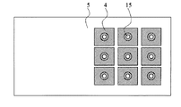
画素電極4は、開口部(画素部ビア)15により背面電極6と接続し、再度、IC部ビア16により出力電極13に接続してある。図2に示すように、画素電極4は長方形又は正方形で、それぞれ独立しており、全ての画素電極4は、出力電極13と背面電極6(図示せず)により、接続されている。駆動用IC11は、金属で形成した突起電極12を用いて、出力電極13と入力電極14に接続してある。
The
第1の基板1は、透明で、厚さ100μmのポリエチレンテレフタレート(PET)フィルムを用い、透明電極2としては、厚さ50nmのITOを用いた。第2の基板5は、厚さ25μmのポリイミドフィルムを用い、厚さ9μmの銅箔を画素電極4と背面電極6に用いた。画素電極4と背面電極6には、厚さ0.5μmの金メッキを施してある。
The
画像表示層3は、図5に示すように、マイクロカプセル20からなり、メタクリル酸樹脂やアラビアゴム等をカプセル殻21とし、内部には酸化チタンからなる白の粒子23とカーボンブラックからなる黒の粒子24が、シリコーンオイル等の粘性の高い分散媒22に分散されて封入されている。カプセル殻21は直径30〜50μmであり、分散している粒子径は、どちらも3〜4μmである。
As shown in FIG. 5, the
白の粒子23は正電荷を帯びており、黒の粒子24は負電荷を帯びている。そのため、図6に示すように、画素電極4と透明電極2に電圧を印加し、画素電極4が負極、透明電極2が正極になった場合、負に帯電した黒の粒子24が透明電極側に引かれるので、透明電極側から観察すると、その部分が黒く表示される。
逆に、画素電極4が正極、透明電極2が負極の場合、正に帯電した白の粒子23が透明電極側に引かれるので、その部分が白く表示される。また、画素電極4と透明電極2への印加電圧を調整することで、中間調表示も可能である。
On the contrary, when the
そして、各粒子は粘性の高い分散媒22に分散されており、一度、電圧を印加した後は、電圧を切断しても粒子の位置が変化せずに表示が残る、いわゆるメモリーを有しており、初期の表示や書き換え時のみ電圧を印加すればよく、大幅な省電力化をはかることが可能である。
Each particle is dispersed in a highly
また、白の粒子23の反射率は、標準白色板に対して40〜50%と高く、さらに散乱特性は、視野角依存性が少ないので、紙の様に明るく見やすい、電子ペーパー表示装置を得ることができる。
Further, the reflectance of the
つぎに、電極に開口部を設けずに、画素電極と背面電極を接続する、いわゆるブラインドビア接続について、図1を用いて説明する。まず、両側に厚さ10μmの銅箔が形成されたポリイミドフィルムを用い、背面電極側に、フォトエッチング工程を用いて、直径50〜100μmの開口部を形成する。そして炭酸ガスレーザー又はYAGレーザーを、背面電極側から、背面電極6の開口部に照射し、第2の基板に穴を形成する。この際、レーザーの出力を、第2の基板の材料であるポリイミドフィルムは溶かすが、画素電極である銅箔は溶かすことができないレベルに調節することで、画素電極4に穴が開かず、ポリイ
ミドフィルムだけに穴を形成することが可能となる。
Next, so-called blind via connection in which the pixel electrode and the back electrode are connected without providing an opening in the electrode will be described with reference to FIG. First, an opening having a diameter of 50 to 100 μm is formed on the back electrode side using a polyimide film in which a copper foil having a thickness of 10 μm is formed on both sides and using a photoetching process. Then, a carbon dioxide laser or YAG laser is irradiated from the back electrode side to the opening of the
つぎに、背面電極側だけ電解メッキあるいは無電解メッキにより厚さ5〜15μmの銅を形成し、画素電極4の裏面と背面電極6を接続することで、第2の基板における開口部が貫通していないブラインドビア接続が完成する。その後、画素電極側にもフォトエッチング工程を行い、画素電極4を形成し、最後に両面に、金メッキあるいは、ニッケル+金メッキを行う。
Next, copper having a thickness of 5 to 15 μm is formed by electrolytic plating or electroless plating only on the back electrode side, and the back surface of the
その後、感光性樹脂や熱硬化性樹脂、あるいはポリイミドフィルムを用いて背面電極保護層7を形成する。なお、必要に応じて、同様に、表面のIC部周辺に表面電極保護層を形成しても良い。
Thereafter, the back electrode
つぎに、表示装置の製造法について説明する。画素電極4と背面電極6及び背面電極保護層7を形成した第2の基板5に、画像表示層3が透明電極2上に塗布された第1の基板1を貼り合わせる。そして、透明でガスや水蒸気の透過しにくい材料を用いて、表面保護フィルム9を貼り合わせて、電気泳動方式の表示装置が完成する。なお、さらに信頼性を向上させるために、裏面保護フィルム8を背面電極保護層の外側に貼り合わせると、より好ましい。なお、裏面保護フィルム8は透明である必要はないので、樹脂フィルムの他に、アルミ箔のような金属薄膜を用いることも可能である。
Next, a method for manufacturing the display device will be described. The
このように形成した電気泳動方式の表示装置は、画素電極4はガスバリア性の良い金属薄膜であり、かつ、貫通したスルーホールが無いので、第2の基板5の外側から進入するガスや水蒸気の進入を抑えることが可能となり、耐湿信頼性の良好な表示装置を得ることができる。
In the electrophoretic display device thus formed, the
以下、本発明の実施例を図面を用いて説明する。図1〜図2は本発明の実施例1を示す図である。図1は本実施例における表示装置の構成要素を説明するための断面図で、 図2は本実施例の表示装置の第2の基板を第1の基板側から見た平面図である。以下、図面を用いて、実施例の表示装置の構成を説明する。
Embodiments of the present invention will be described below with reference to the drawings. 1 to 2 are
本実施例の表示装置は、第2の基板の開口部には、背面電極が開口部を埋めるように配置されたブラインドビア接続を用いたことと、駆動用ICを画素電極と同じ側に配置したことを特徴とする。図1に示すように、透明電極2を表示領域全面に備えた透明な材料からなる第1の基板1と、金属薄膜からなる画素電極4を備えた第2の基板5と、マイクロカプセルからなる画像表示層3から構成されており、第2の基板5の裏面には背面電極6設けてあり、画素電極4と背面電極6は第2の基板における開口部15(画素部ビア)で接続されており、さらに出力電極13も背面電極6とIC部ビア16で接続されている。
In the display device of this embodiment, the opening of the second substrate uses the blind via connection in which the back electrode is arranged so as to fill the opening, and the driving IC is arranged on the same side as the pixel electrode. It is characterized by that. As shown in FIG. 1, a
第1の基板1としては、厚さ100μmのPETフィルムを用い、透明電極2は、厚さ0.5μmのITOをスパッタリング法で形成した。画素電極4と背面電極6は、厚さ10μmの銅薄膜を用い、厚さ3μmのニッケルメッキと厚さ0.5μmの金メッキ処理を行った。第2の基板5は、厚さ25μmのポリイミドフィルムを用いた。さらに、背面電極6を保護するために、厚さ20μmの背面電極保護層7を熱硬化型ハンダレジストを用いてスクリーン印刷法で形成した。
As the
画像表示層3は、前述したように、透明な分散媒と、正に帯電した白粒子と、負に帯電した黒粒子が封入されてマイクロカプセルからなる。
As described above, the
画像表示層3が透明電極2上に塗布されている第1の基板1を、パターンニング工程が
完了した第2の基板5に圧着し、さらに、裏面保護フィルム8と表面保護フィルム9で、表示部全体を保護している。表面保護フィルム9には、ガスバリア層をコートした厚さ100μmのPETをフィルムを用い、裏面保護フィルム8も、表面保護フィルムと同一材料を用い、どちらも熱硬化性の粘着層を用いて接着した。
The
なお、図7に示した従来技術と同様に、画像表示層3にガスバリア層25と接着層26を設け、この接着層26を用いて画素電極4と接続することも可能である。
As in the prior art shown in FIG. 7, the
画素電極4と駆動用IC11の出力電極13をそれぞれ接続するスタチック駆動を用いているので、画素電極4は、図2に示したように長方形又は正方形であり、透明電極2は、パターンニングしておらず、第1の基板1の全面にある。また、第2の基板5には、画素電極4と同一面に、出力電極13と入力電極14を形成してあり、出力電極13は、IC部ビア16を用いて、背面電極6と接続してある。
Since the static drive that connects the
ここで、第2の基板5は、前述した製造法を用いたブラインドビア接続により、画素電極4には穴を設けず、第2の基板の開口部を埋めるように、背面電極6を設けて第2の基板における開口部(画素部ビア)15で接続し、同時に、出力電極13にも穴を設けずに背面電極6とIC部ビア16で接続してある。第2の基板における画像表示層側からは、第2の基板における開口部(画素部ビア)15およびIC部ビア16は基板の裏面側にあるため、見ることはできないが、図2ではそれらを透視した状態で、それぞれの位置を丸印で示してある。
Here, the
最後に、突起電極12を形成してある駆動用IC11を、異方導電フィルム又は金属熱圧接で入力電極14と出力電極13とに接続して、表示装置が完成した。
Finally, the driving
この表示装置は、画素電極4に貫通したスルーホールが開いていなく、金属薄膜である画素電極4および背面電極6がガスバリア層としてはたらくので、50゜C90%の高温高湿度試験において、20日間放置しても、良好な特性が得られた。なお、画素電極間に30〜50μmの隙間があり、第2の基板5を透過した水蒸気が進入するが、この部分は非表示部であるので、影響は少ない。
In this display device, the through-hole penetrating the
また、このブラインドビア接続を用いた第2の基板を用いたことで、出力電極13のピッチは100〜150μmと狭くすることが可能となり、その結果、単位面積あたりの画素数が多い、高密度表示の電気泳動方式表示装置を作成することが可能となった。
Further, by using the second substrate using this blind via connection, the pitch of the
また、第2の基板として、厚さ25μmと薄く、柔軟性のあるフィルムを用いたことで、ガラス基板を用いたTFTタイプと比較して、薄く、軽く、かつ、湾曲させることも可能な表示装置を実現できた。 In addition, a thin, flexible film with a thickness of 25 μm is used as the second substrate, so that the display can be made thinner, lighter, and curved compared to a TFT type using a glass substrate. The device was realized.
このように、透明電極を備える第1の基板と、画素電極と背面電極を備える第2の基板と、電気泳動により動作する画像表示層を備え、かつ、画素電極には開口部を設けずに第2の基板に設けた穴を通して背面電極と接続するブラインドビア接続による第2の基板を用いることにより、ガスや水蒸気の画像表示層への進入を抑えて、耐湿信頼性が良好で、かつ、高密度表示が可能である、電気泳動方式の表示装置を得られた。 As described above, the first substrate including the transparent electrode, the second substrate including the pixel electrode and the back electrode, the image display layer that operates by electrophoresis, and the pixel electrode without an opening. By using the second substrate by the blind via connection that connects to the back electrode through the hole provided in the second substrate, the entry of gas or water vapor into the image display layer is suppressed, the moisture resistance reliability is good, and An electrophoretic display device capable of high-density display was obtained.
この表示装置は、第2の基板にも樹脂フィルムを用いたので、軽く、薄く、曲げることも可能であり、マイクロカプセル方式の電気泳動方式の特徴であるメモリー性により消費電力が少なく、かつ、明るく視野角特性が良好な反射表示が得られた。 Since this display device also uses a resin film for the second substrate, it is light, thin, and can be bent, and it has low power consumption due to the memory property that is characteristic of the microcapsule electrophoresis method, and A bright reflective display with good viewing angle characteristics was obtained.
本実施例では、画像表示層として、黒と白の2種類の粒子を含んだマイクロカプセルを
用いたが、着色分散媒中に少なくとも1種類の電気泳動粒子を分散させ封入したマイクロカプセルを用いることも可能である。また、本実施例では、白と黒の微粒子を用いたが、他の色の粒子を封入したマイクロカプセルを用いることも可能である。例えば、赤粒子と白粒子を用いることで、白表示の中に、赤い文字を表示することが可能である。
In this embodiment, a microcapsule containing two types of black and white particles is used as the image display layer. However, a microcapsule in which at least one type of electrophoretic particles is dispersed and enclosed in a colored dispersion medium is used. Is also possible. In this embodiment, white and black fine particles are used. However, microcapsules enclosing particles of other colors can be used. For example, by using red particles and white particles, it is possible to display red characters in the white display.
本実施例では、画像表示層として、黒と白の2種類の粒子を含んだマクロカプセルを用いたが、着色分散媒中に少なくとも1種類の電気泳動粒子を分散させ封入したマイクロカプセルを用いることも可能である。例えば、青色の染料を分散媒に溶解し、白色の粒子を封入したマイクロカプセルを用いることで、白背景に青文字の表示装置を得ることができた。 In this embodiment, a macrocapsule containing two types of black and white particles is used as the image display layer. However, a microcapsule in which at least one type of electrophoretic particle is dispersed and enclosed in a colored dispersion medium is used. Is also possible. For example, by using a microcapsule in which a blue dye is dissolved in a dispersion medium and white particles are encapsulated, a blue character display device can be obtained on a white background.
本実施例では、第2の基板として、25ミクロンのポリイミドフィルムを用いたが、厚さは9〜50μmの材料が使用可能である。また、液晶ポリマーフィルムを用いることも可能である。 In this example, a 25-micron polyimide film was used as the second substrate, but a material with a thickness of 9 to 50 μm can be used. It is also possible to use a liquid crystal polymer film.
本実施例では、画像表示層としてマイクロカプセルを用いたが、第1の基板と第2の基板の間に多数の隔壁を設け、その隔壁内に着色した分散媒と、少なくとも1種類の帯電した粒子を封入しても、同様な表示装置が得られる。また、画像表示層として、第1の基板と第2の基板の間に多数の隔壁を設け、分散媒は使用せず、その隔壁内に、正負に帯電した白と黒の微粒子を封入した粉体流動を用いることも可能である。 In this embodiment, microcapsules are used as the image display layer. However, a large number of partition walls are provided between the first substrate and the second substrate, and the dispersion medium colored in the partition walls is charged with at least one kind of charge. Even if the particles are enclosed, a similar display device can be obtained. Further, as an image display layer, a powder in which a large number of partition walls are provided between the first substrate and the second substrate, no dispersion medium is used, and positive and negative charged white and black fine particles are enclosed in the partition walls. It is also possible to use body flow.
つぎに、本発明における実施例2の表示装置の構成について説明する。本実施例の表示装置は、背面電極には穴が無く、画素電極が第2の基板における開口部を埋めるように設けたブラインドビア接続を用いていることと、駆動用ICを背面電極と同じ側に配置したことが、実施例1の構成と異なっている。 Next, the configuration of the display device according to the second embodiment of the present invention will be described. In the display device of this embodiment, the back electrode has no hole, the pixel electrode uses the blind via connection provided to fill the opening in the second substrate, and the driving IC is the same as the back electrode. The arrangement on the side is different from the configuration of the first embodiment.
本実施例における表示装置の構成を、図面を用いて説明する。図3は本実施例における表示装置の構成要素を説明するための断面図で、 図4は実施例におけるの表示装置の第2の基板を第1の基板側から見た平面図である。 The structure of the display device in this embodiment will be described with reference to the drawings. FIG. 3 is a cross-sectional view for explaining the components of the display device according to the present embodiment. FIG. 4 is a plan view of the second substrate of the display device according to the present embodiment as viewed from the first substrate side.
本実施例の表示装置は、図3に示すように、透明電極2を備えた透明な材料からなる第1の基板1と、金属薄膜からなる画素電極4を備えた第2の基板5と、マイクロカプセルからなる画像表示層3から構成されており、第2の基板5の裏面には背面電極6設けてあり、画素電極4と背面電極6は第2の基板における開口部(画素部ビア)15で接続されている。出力電極13は、背面電極側に形成してあり、背面電極6と直接、接続されている。
As shown in FIG. 3, the display device of this example includes a
第1の基板1、透明電極2、及び画像表示層3は、実施例1と同一材料を用いた。第2の基板も、画素電極4と背面電極6の接続方式は異なるが、それ以外は、全て同一材料を用いて作成した。
For the
画素電極4は、図4に示した様に長方形又は正方形とした。透明電極2は、パターンニングしておらず、第1の基板1の全面にある。また、第2の基板5には、駆動用IC11を接続するために、出力電極13と入力電極14を、背面電極側に形成してある。
The
ここで、第2の基板5は、前述したブラインドビア接続の製造法と同様に製造したが、実施例1とは逆に、背面電極6には開口部を設けず、画素電極4に開口部を設けて画素部ビア15で接続した。駆動用IC11を、背面電極側に配置したので、実施例1で用いたIC部ビアは不要となり、その分の穴開け加工が減り、製造コストを減らすことができる
。
Here, the
なお、画素電極4に、一旦、穴を設けたが、背面電極6と接続するために、画素電極とつながるように銅メッキを行った際に、第2の基板の開口部が銅メッキ膜の画素電極で埋まり、ガスや水蒸気の進入を防ぐことが可能となる。
Although the
最後に、突起電極12を形成してある駆動用IC11を、異方導電フィルム又は金属熱圧接で入力電極14と出力電極13とに接続して、表示装置が完成した。但し、実施例1と異なり、駆動用ICは、背面電極側に接続してある。
Finally, the driving
この本実施例の表示装置も、第2の基板における開口部(画素部ビア)15が銅メッキでふさがれているので、金属薄膜である画素電極4および背面電極6がガスバリア層としてはたらき、50゜C度90%の高温高湿度試験において、20日間放置しても、良好な特性が得られた。なお、画素電極4には、銅メッキ後も、直径40〜60μmで深さ10μm程度の小さな凹みが残っているが、粉体粒子の解像度も50〜60μm程度であるので、凹みの部分も画素電極と同じ表示色となり、表示上の問題は、全くなかった。
Also in the display device of this embodiment, since the opening (pixel portion via) 15 in the second substrate is covered with copper plating, the
また、本実施例の第2の基板は、画素電極側に銅メッキを行い、背面電極側には銅メッキ処理を行わなくて済むので、背面電極や出力電極のピッチは、実施例1より小さく、50〜100μmと狭くすることが可能となり、その結果、さらに高密度表示の電気泳動方式の表示装置を作成することができた。 Further, since the second substrate of this embodiment does not require copper plating on the pixel electrode side and copper plating on the back electrode side, the pitch of the back electrodes and output electrodes is smaller than that of the first embodiment. As a result, it was possible to produce an electrophoretic display device with a higher density display.
このように、透明電極を備える第1の基板と、画素電極と背面電極を備える第2の基板と、電気泳動により動作する画像表示層を備え、かつ、背面電極には穴を設けずに第2の基板に設けた開口部を埋めた画素電極と接続するブラインドビア接続による第2の基板を用いることにより、ガスや水蒸気の進入を抑えて、耐湿信頼性が良好で、かつ、高密度表示が可能である、電気泳動方式の表示装置を得られた。
As described above, the first substrate including the transparent electrode, the second substrate including the pixel electrode and the back electrode, the image display layer that operates by electrophoresis, and the back electrode without the holes are provided in the first substrate. By using a second substrate with a blind via connection that connects to a pixel electrode in which an opening provided in the
この表示装置は実施例1の表示装置と同様に、第2の基板にも樹脂フィルムを用いたので、軽く、薄く、湾曲させることも可能であり、マイクロカプセル方式の電気泳動方式の特徴であるメモリー性により消費電力が少なく、かつ、明るく視野角特性が良好な反射表示が得られた。 Since this display device uses a resin film for the second substrate in the same manner as the display device of the first embodiment, it can be light, thin and curved, and is characteristic of the microcapsule electrophoresis method. Reflective display with low power consumption due to its memory characteristics and bright and good viewing angle characteristics was obtained.
以上の説明から明らかなように、本発明によれば、画素電極あるいは背面電極のどちらか一方の電極によって、第2の基板に設けた開口部を埋め、画素電極と背面電極を電気的接続するブラインドビア接続を用いることで、耐湿信頼性が良好で、かつ、薄く柔軟性がある電気泳動方式の表示装置を提供できる。 As is clear from the above description, according to the present invention, the opening provided in the second substrate is filled with either the pixel electrode or the back electrode, and the pixel electrode and the back electrode are electrically connected. By using the blind via connection, it is possible to provide an electrophoretic display device having good moisture resistance reliability and being thin and flexible.
1 第1の基板
2 透明電極
3 画像表示層
4 画素電極
5 第2の基板
6 背面電極
7 背面電極保護層
8 裏面保護フィルム
9 表面保護フィルム
11 駆動用IC
12 突起電極
13 出力電極
14 入力電極
15 開口部(画素部ビア)
16 IC部ビア
20 マイクロカプセル
21 カプセル殻
22 分散媒
23 白の粒子
24 黒の粒子
25 バリア層
26 接着層
DESCRIPTION OF
12
16 IC part via 20
Claims (8)
As the image display layer, a large number of partition walls are provided between the first substrate and the second substrate, and no dispersion medium is used, and at least two kinds of charged particles having different colors are sealed between the partition walls. The display device according to claim 1.
Priority Applications (1)
| Application Number | Priority Date | Filing Date | Title |
|---|---|---|---|
| JP2004298357A JP4589690B2 (en) | 2004-10-13 | 2004-10-13 | Display device |
Applications Claiming Priority (1)
| Application Number | Priority Date | Filing Date | Title |
|---|---|---|---|
| JP2004298357A JP4589690B2 (en) | 2004-10-13 | 2004-10-13 | Display device |
Publications (3)
| Publication Number | Publication Date |
|---|---|
| JP2006113157A JP2006113157A (en) | 2006-04-27 |
| JP2006113157A5 JP2006113157A5 (en) | 2008-01-31 |
| JP4589690B2 true JP4589690B2 (en) | 2010-12-01 |
Family
ID=36381745
Family Applications (1)
| Application Number | Title | Priority Date | Filing Date |
|---|---|---|---|
| JP2004298357A Expired - Fee Related JP4589690B2 (en) | 2004-10-13 | 2004-10-13 | Display device |
Country Status (1)
| Country | Link |
|---|---|
| JP (1) | JP4589690B2 (en) |
Families Citing this family (12)
| Publication number | Priority date | Publication date | Assignee | Title |
|---|---|---|---|---|
| JP2007334126A (en) * | 2006-06-16 | 2007-12-27 | Mitsubishi Pencil Co Ltd | Electrophoretic display device |
| JP2008033094A (en) * | 2006-07-31 | 2008-02-14 | Toppan Printing Co Ltd | Display device |
| JP2008033095A (en) * | 2006-07-31 | 2008-02-14 | Toppan Printing Co Ltd | Display device |
| JP5069450B2 (en) * | 2006-11-17 | 2012-11-07 | トッパン・フォームズ株式会社 | Method for manufacturing electrode substrate for display device |
| JP5069451B2 (en) * | 2006-11-17 | 2012-11-07 | トッパン・フォームズ株式会社 | Method for manufacturing electrode substrate for display device |
| TWI361331B (en) * | 2007-06-01 | 2012-04-01 | Pervasive Display Co Ltd | E-paper apparatus |
| JP5087374B2 (en) * | 2007-11-28 | 2012-12-05 | トッパン・フォームズ株式会社 | Method for manufacturing electrode substrate for display device |
| US20110261434A1 (en) * | 2008-12-18 | 2011-10-27 | Bridgestone Corporation | Information display panel |
| JP5824844B2 (en) * | 2011-04-18 | 2015-12-02 | 大日本印刷株式会社 | Back electrode substrate for electronic paper and electronic paper |
| JP2013222087A (en) * | 2012-04-17 | 2013-10-28 | Seiko Epson Corp | Electrophoretic display device and manufacturing method for the same |
| US10317767B2 (en) | 2014-02-07 | 2019-06-11 | E Ink Corporation | Electro-optic display backplane structure with drive components and pixel electrodes on opposed surfaces |
| WO2018187077A1 (en) * | 2017-04-07 | 2018-10-11 | E Ink Corporation | Electro-optic display backplane structures with drive components and pixel electrodes on opposed surfaces |
Citations (2)
| Publication number | Priority date | Publication date | Assignee | Title |
|---|---|---|---|---|
| JPS6242129A (en) * | 1985-08-20 | 1987-02-24 | Fujitsu Ltd | Electrochromic display element |
| JPH06242457A (en) * | 1993-02-19 | 1994-09-02 | Hitachi Ltd | Reflection type liquid crystal display |
-
2004
- 2004-10-13 JP JP2004298357A patent/JP4589690B2/en not_active Expired - Fee Related
Patent Citations (2)
| Publication number | Priority date | Publication date | Assignee | Title |
|---|---|---|---|---|
| JPS6242129A (en) * | 1985-08-20 | 1987-02-24 | Fujitsu Ltd | Electrochromic display element |
| JPH06242457A (en) * | 1993-02-19 | 1994-09-02 | Hitachi Ltd | Reflection type liquid crystal display |
Also Published As
| Publication number | Publication date |
|---|---|
| JP2006113157A (en) | 2006-04-27 |
Similar Documents
| Publication | Publication Date | Title |
|---|---|---|
| CN106211793B (en) | Multilayer extended electrode structure for backplane assembly | |
| CN104583853B (en) | For the technique for producing electro-optic displays | |
| JP2006113436A (en) | Display device | |
| JP4589690B2 (en) | Display device | |
| KR100516597B1 (en) | Semiconductor device, semiconductor device mounting structure, liquid crystal device, and electronic apparatus | |
| KR101201658B1 (en) | Information display apparatus | |
| CN106133816A (en) | The back board structure of electro-optic displays | |
| US20020044251A1 (en) | Image device | |
| US6236442B1 (en) | Method of making liquid crystal display having patterned conductive images | |
| JP4234848B2 (en) | Display media | |
| JP2006017750A (en) | Electrophoretic display device and method for manufacturing the same | |
| JP2013222087A (en) | Electrophoretic display device and manufacturing method for the same | |
| JP2004109449A5 (en) | ||
| JP5087374B2 (en) | Method for manufacturing electrode substrate for display device | |
| JP2010085743A (en) | Method of driving display device, the display device and electronic apparatus | |
| CN210051987U (en) | Block type multicolor display electrophoretic display device | |
| JP2006023089A (en) | Front plate defect measuring apparatus | |
| JP3286587B2 (en) | Liquid crystal panel and luminescent matrix panel | |
| JP5069450B2 (en) | Method for manufacturing electrode substrate for display device | |
| JP2006330528A (en) | Electrodeposition type display device | |
| JP5069451B2 (en) | Method for manufacturing electrode substrate for display device | |
| KR20070121212A (en) | Printed circuit board and liquid crystal display including the same | |
| JP4432589B2 (en) | Electro-optical device, method of manufacturing electro-optical device, and electronic apparatus | |
| JP2008225037A (en) | Electrophoretic display panel sealing structure | |
| CN112578605A (en) | Electronic paper packaging structure, packaging method and electronic device |
Legal Events
| Date | Code | Title | Description |
|---|---|---|---|
| A621 | Written request for application examination |
Free format text: JAPANESE INTERMEDIATE CODE: A621 Effective date: 20070612 |
|
| RD03 | Notification of appointment of power of attorney |
Free format text: JAPANESE INTERMEDIATE CODE: A7423 Effective date: 20070612 |
|
| A521 | Request for written amendment filed |
Free format text: JAPANESE INTERMEDIATE CODE: A523 Effective date: 20071212 |
|
| TRDD | Decision of grant or rejection written | ||
| A01 | Written decision to grant a patent or to grant a registration (utility model) |
Free format text: JAPANESE INTERMEDIATE CODE: A01 Effective date: 20100907 |
|
| A01 | Written decision to grant a patent or to grant a registration (utility model) |
Free format text: JAPANESE INTERMEDIATE CODE: A01 |
|
| A61 | First payment of annual fees (during grant procedure) |
Free format text: JAPANESE INTERMEDIATE CODE: A61 Effective date: 20100910 |
|
| R150 | Certificate of patent or registration of utility model |
Ref document number: 4589690 Country of ref document: JP Free format text: JAPANESE INTERMEDIATE CODE: R150 Free format text: JAPANESE INTERMEDIATE CODE: R150 |
|
| FPAY | Renewal fee payment (event date is renewal date of database) |
Free format text: PAYMENT UNTIL: 20130917 Year of fee payment: 3 |
|
| S111 | Request for change of ownership or part of ownership |
Free format text: JAPANESE INTERMEDIATE CODE: R313113 |
|
| R350 | Written notification of registration of transfer |
Free format text: JAPANESE INTERMEDIATE CODE: R350 |
|
| R250 | Receipt of annual fees |
Free format text: JAPANESE INTERMEDIATE CODE: R250 |
|
| R250 | Receipt of annual fees |
Free format text: JAPANESE INTERMEDIATE CODE: R250 |
|
| LAPS | Cancellation because of no payment of annual fees |