JP4391564B2 - 単芯光ファイバーケーブルを用いる双方向光トランシーバーモジュール - Google Patents
単芯光ファイバーケーブルを用いる双方向光トランシーバーモジュール Download PDFInfo
- Publication number
- JP4391564B2 JP4391564B2 JP2007516378A JP2007516378A JP4391564B2 JP 4391564 B2 JP4391564 B2 JP 4391564B2 JP 2007516378 A JP2007516378 A JP 2007516378A JP 2007516378 A JP2007516378 A JP 2007516378A JP 4391564 B2 JP4391564 B2 JP 4391564B2
- Authority
- JP
- Japan
- Prior art keywords
- module
- lens
- light
- optical
- optical fiber
- Prior art date
- Legal status (The legal status is an assumption and is not a legal conclusion. Google has not performed a legal analysis and makes no representation as to the accuracy of the status listed.)
- Expired - Fee Related
Links
- 230000003287 optical effect Effects 0.000 title claims description 119
- 239000013307 optical fiber Substances 0.000 title claims description 33
- 230000005540 biological transmission Effects 0.000 claims description 50
- 230000002457 bidirectional effect Effects 0.000 claims description 15
- 238000001746 injection moulding Methods 0.000 claims description 11
- 239000004033 plastic Substances 0.000 claims description 9
- 229920003023 plastic Polymers 0.000 claims description 9
- 230000008878 coupling Effects 0.000 claims 1
- 238000010168 coupling process Methods 0.000 claims 1
- 238000005859 coupling reaction Methods 0.000 claims 1
- 239000012780 transparent material Substances 0.000 claims 1
- 239000002184 metal Substances 0.000 description 19
- 238000000034 method Methods 0.000 description 15
- 238000004891 communication Methods 0.000 description 9
- XUIMIQQOPSSXEZ-UHFFFAOYSA-N Silicon Chemical compound [Si] XUIMIQQOPSSXEZ-UHFFFAOYSA-N 0.000 description 8
- 229910052710 silicon Inorganic materials 0.000 description 8
- 239000010703 silicon Substances 0.000 description 8
- 238000004519 manufacturing process Methods 0.000 description 6
- 239000004065 semiconductor Substances 0.000 description 5
- 239000000853 adhesive Substances 0.000 description 4
- 230000001070 adhesive effect Effects 0.000 description 4
- 238000003780 insertion Methods 0.000 description 3
- 230000037431 insertion Effects 0.000 description 3
- 239000000463 material Substances 0.000 description 3
- 239000000243 solution Substances 0.000 description 3
- 230000000903 blocking effect Effects 0.000 description 2
- 239000003990 capacitor Substances 0.000 description 2
- 238000006243 chemical reaction Methods 0.000 description 2
- 230000005611 electricity Effects 0.000 description 2
- 238000005530 etching Methods 0.000 description 2
- 239000000835 fiber Substances 0.000 description 2
- 238000012986 modification Methods 0.000 description 2
- 230000004048 modification Effects 0.000 description 2
- 229920003229 poly(methyl methacrylate) Polymers 0.000 description 2
- 239000004926 polymethyl methacrylate Substances 0.000 description 2
- 239000000758 substrate Substances 0.000 description 2
- 239000010409 thin film Substances 0.000 description 2
- 239000004593 Epoxy Substances 0.000 description 1
- 238000001514 detection method Methods 0.000 description 1
- 238000010586 diagram Methods 0.000 description 1
- 239000000428 dust Substances 0.000 description 1
- 238000000206 photolithography Methods 0.000 description 1
- 239000004417 polycarbonate Substances 0.000 description 1
- 229920000515 polycarbonate Polymers 0.000 description 1
- 230000035945 sensitivity Effects 0.000 description 1
- 238000000926 separation method Methods 0.000 description 1
- 238000003860 storage Methods 0.000 description 1
- 238000003466 welding Methods 0.000 description 1
Images


Classifications
-
- G—PHYSICS
- G02—OPTICS
- G02B—OPTICAL ELEMENTS, SYSTEMS OR APPARATUS
- G02B6/00—Light guides; Structural details of arrangements comprising light guides and other optical elements, e.g. couplings
- G02B6/24—Coupling light guides
- G02B6/42—Coupling light guides with opto-electronic elements
-
- G—PHYSICS
- G02—OPTICS
- G02B—OPTICAL ELEMENTS, SYSTEMS OR APPARATUS
- G02B6/00—Light guides; Structural details of arrangements comprising light guides and other optical elements, e.g. couplings
- G02B6/24—Coupling light guides
- G02B6/42—Coupling light guides with opto-electronic elements
- G02B6/4201—Packages, e.g. shape, construction, internal or external details
- G02B6/4255—Moulded or casted packages
-
- G—PHYSICS
- G02—OPTICS
- G02B—OPTICAL ELEMENTS, SYSTEMS OR APPARATUS
- G02B6/00—Light guides; Structural details of arrangements comprising light guides and other optical elements, e.g. couplings
- G02B6/24—Coupling light guides
- G02B6/42—Coupling light guides with opto-electronic elements
- G02B6/4201—Packages, e.g. shape, construction, internal or external details
- G02B6/4274—Electrical aspects
- G02B6/4277—Protection against electromagnetic interference [EMI], e.g. shielding means
-
- G—PHYSICS
- G02—OPTICS
- G02B—OPTICAL ELEMENTS, SYSTEMS OR APPARATUS
- G02B6/00—Light guides; Structural details of arrangements comprising light guides and other optical elements, e.g. couplings
- G02B6/24—Coupling light guides
- G02B6/42—Coupling light guides with opto-electronic elements
- G02B6/4201—Packages, e.g. shape, construction, internal or external details
- G02B6/4204—Packages, e.g. shape, construction, internal or external details the coupling comprising intermediate optical elements, e.g. lenses, holograms
- G02B6/4206—Optical features
-
- G—PHYSICS
- G02—OPTICS
- G02B—OPTICAL ELEMENTS, SYSTEMS OR APPARATUS
- G02B6/00—Light guides; Structural details of arrangements comprising light guides and other optical elements, e.g. couplings
- G02B6/24—Coupling light guides
- G02B6/42—Coupling light guides with opto-electronic elements
- G02B6/4201—Packages, e.g. shape, construction, internal or external details
- G02B6/4204—Packages, e.g. shape, construction, internal or external details the coupling comprising intermediate optical elements, e.g. lenses, holograms
- G02B6/4214—Packages, e.g. shape, construction, internal or external details the coupling comprising intermediate optical elements, e.g. lenses, holograms the intermediate optical element having redirecting reflective means, e.g. mirrors, prisms for deflecting the radiation from horizontal to down- or upward direction toward a device
-
- G—PHYSICS
- G02—OPTICS
- G02B—OPTICAL ELEMENTS, SYSTEMS OR APPARATUS
- G02B6/00—Light guides; Structural details of arrangements comprising light guides and other optical elements, e.g. couplings
- G02B6/24—Coupling light guides
- G02B6/42—Coupling light guides with opto-electronic elements
- G02B6/4201—Packages, e.g. shape, construction, internal or external details
- G02B6/4246—Bidirectionally operating package structures
-
- H—ELECTRICITY
- H01—ELECTRIC ELEMENTS
- H01L—SEMICONDUCTOR DEVICES NOT COVERED BY CLASS H10
- H01L2224/00—Indexing scheme for arrangements for connecting or disconnecting semiconductor or solid-state bodies and methods related thereto as covered by H01L24/00
- H01L2224/01—Means for bonding being attached to, or being formed on, the surface to be connected, e.g. chip-to-package, die-attach, "first-level" interconnects; Manufacturing methods related thereto
- H01L2224/42—Wire connectors; Manufacturing methods related thereto
- H01L2224/47—Structure, shape, material or disposition of the wire connectors after the connecting process
- H01L2224/48—Structure, shape, material or disposition of the wire connectors after the connecting process of an individual wire connector
- H01L2224/4805—Shape
- H01L2224/4809—Loop shape
- H01L2224/48091—Arched
-
- H—ELECTRICITY
- H01—ELECTRIC ELEMENTS
- H01L—SEMICONDUCTOR DEVICES NOT COVERED BY CLASS H10
- H01L2224/00—Indexing scheme for arrangements for connecting or disconnecting semiconductor or solid-state bodies and methods related thereto as covered by H01L24/00
- H01L2224/01—Means for bonding being attached to, or being formed on, the surface to be connected, e.g. chip-to-package, die-attach, "first-level" interconnects; Manufacturing methods related thereto
- H01L2224/42—Wire connectors; Manufacturing methods related thereto
- H01L2224/47—Structure, shape, material or disposition of the wire connectors after the connecting process
- H01L2224/48—Structure, shape, material or disposition of the wire connectors after the connecting process of an individual wire connector
- H01L2224/481—Disposition
- H01L2224/48151—Connecting between a semiconductor or solid-state body and an item not being a semiconductor or solid-state body, e.g. chip-to-substrate, chip-to-passive
- H01L2224/48221—Connecting between a semiconductor or solid-state body and an item not being a semiconductor or solid-state body, e.g. chip-to-substrate, chip-to-passive the body and the item being stacked
- H01L2224/48245—Connecting between a semiconductor or solid-state body and an item not being a semiconductor or solid-state body, e.g. chip-to-substrate, chip-to-passive the body and the item being stacked the item being metallic
- H01L2224/48247—Connecting between a semiconductor or solid-state body and an item not being a semiconductor or solid-state body, e.g. chip-to-substrate, chip-to-passive the body and the item being stacked the item being metallic connecting the wire to a bond pad of the item
Landscapes
- Physics & Mathematics (AREA)
- General Physics & Mathematics (AREA)
- Optics & Photonics (AREA)
- Electromagnetism (AREA)
- Optical Couplings Of Light Guides (AREA)
- Semiconductor Lasers (AREA)
- Optical Communication System (AREA)
Description
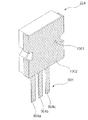
204、204b 発光デバイス
205、205b 受光デバイス
207 送信ケーブル
211 送信レンズ
212 受信レンズ
213 レセプタクルレンズ
221 レンズモジュール
222 フィルターモジュール
223 送信モジュール
224 受信モジュール
422、423、424 挿入部分
433、434 ガイドピン
501 ベース
801 ガイド溝
802 金属のワイヤー
804a、804b、904a、904b、904c、911 メタルリードフレーム
903 受信モジュールの本体
905 プリアンプIC
906 コンデンサー
1001 スルーホール
Claims (10)
- 発光デバイスを含んだ光送信モジュール;受光デバイスを含んだ光受信モジュール;送信された光と受信された光を、送信する光を前述の光送信モジュールから光ケーブルに向かって導き、そして受信した光を前述の光ケーブルから導くことによって分けるフィルターモジュール;そして単芯光ファイバーケーブルを使用した双方向光トランシーバーモジュールは、双方向光トランシーバーモジュールを光学的に位置合わせするレンズモジュールを含み、前記レンズモジュールは、光ファイバーケーブルを接続している容器;特定の位置で、レンズモジュールと送信モジュールを接続している第1接続部;特定の位置で、レンズモジュールと受信モジュールを接続している第2接続部; そして特定の位置でレンズモジュールとフィルターモジュールを接続している第3接続部、を含み、かつ、光送信レンズを含んだレンズモジュールは、発光デバイスからの発光を平行にする光送信レンズ;光ファイバーケーブルからの光を集め、前述の受光デバイスに集光する光受信レンズ;そして前述の発光デバイスからの光を集め、前述の光ファイバーケーブルへ集光する、光トランシーバーモジュール側へ向かって前述の光ファイバーケーブルからの発光を平行にするレセプタクルレンズ、を含み、送信レンズ、受信レンズ、レセプタクルレンズ、レンズモジュール内のレセプタクルは、透明な素材で一つのボディーを形成している単芯光ファイバーケーブルを使用した双方向光トランシーバーモジュール。
- 光送信モジュール、光受信モジュール、レンズモジュール、フィルターモジュールはプラスチック射出成型で、それぞれ、組み立てられた請求項1記載の単芯光ファイバーケーブルを使用した双方向光トランシーバーモジュール。
- フィルターモジュールは、第一波長光を送信し、第一波長光とは異なる第二波長光を反射する請求項1記載の単芯光ファイバーケーブルを使用した双方向光トランシーバーモジュール。
- 第1接続部は、レンズモジュールか送信モジュールのいずれかで形成されたガイドピンを含み;そして前述のレンズモジュールか送信モジュールのいずれかで形成されたガイド溝を含む請求項1記載の単芯光ファイバーケーブルを使用した双方向光トランシーバーモジュール。
- 第2接続部は、レンズモジュールまたは送信モジュールに形成されたガイドピンを含み;そして前述のレンズモジュールまたは送信モジュールで形成されたガイド溝を含む請求項1記載の単芯光ファイバーケーブルを使用した双方向光トランシーバーモジュール。
- 第3接続部は、フィルターモジュールとレンズモジュールを結合するためのレンズモジュールの溝を含み、そして前述のフィルターモジュールの上部は、レンズモジュールの前述の溝に挿入され固定される請求項1記載の単芯光ファイバーケーブルを使用した双方向光トランシーバーモジュール。
- レンズモジュールと送信モジュールが、第1の接続部によって接続している、前述の送信モジュールは送信レンズの中心に一致する位置にある溝を含む;そして、前述の発光デバイスは溝に挿入され、発光デバイスからの光は送信レンズの中心に入射する請求項1記載の単芯光ファイバーケーブルを使用した双方向光トランシーバーモジュール。
- レンズモジュールと受信モジュールが、第2の接続部によって接続している、前述の受信モジュールは受信レンズの中心に一致する位置にある溝を含み;そして、受光デバイスは溝に挿入され、受光レンズからの光は受光デバイスの中心に入射する請求項1記載の単芯光ファイバーケーブルを使用した双方向光トランシーバーモジュール。
- 受信モジュールは静電遮蔽のためのリードフレーム部品を含み、受光デバイスと電気装置を挿入した後、遮蔽の為の部品を折りたたみ、受信モジュールの上部表面をカバーすることにより、静電遮蔽を具現化する請求項1記載の単芯光ファイバーケーブルを使用した双方向光トランシーバーモジュール。
- 送信モジュールは静電遮蔽のためのリードフレーム部品を含み、発光デバイスを挿入した後、遮蔽の為の部品を折りたたみ、送信モジュールの上部表面をカバーすることにより、静電遮蔽を具現化する請求項1記載の単芯光ファイバーケーブルを使用した双方向光トランシーバーモジュール。
Applications Claiming Priority (2)
| Application Number | Priority Date | Filing Date | Title |
|---|---|---|---|
| KR1020040047869A KR100646599B1 (ko) | 2004-06-24 | 2004-06-24 | 단일 광케이블을 이용한 양방향 광 송수신 모듈 |
| PCT/KR2005/001590 WO2006001606A1 (en) | 2004-06-24 | 2005-05-28 | Bidirectional optical transceiver module using a single optical fiber cable |
Publications (2)
| Publication Number | Publication Date |
|---|---|
| JP2008512694A JP2008512694A (ja) | 2008-04-24 |
| JP4391564B2 true JP4391564B2 (ja) | 2009-12-24 |
Family
ID=35781987
Family Applications (1)
| Application Number | Title | Priority Date | Filing Date |
|---|---|---|---|
| JP2007516378A Expired - Fee Related JP4391564B2 (ja) | 2004-06-24 | 2005-05-28 | 単芯光ファイバーケーブルを用いる双方向光トランシーバーモジュール |
Country Status (5)
| Country | Link |
|---|---|
| US (1) | US20090202244A1 (ja) |
| JP (1) | JP4391564B2 (ja) |
| KR (1) | KR100646599B1 (ja) |
| CN (1) | CN100516954C (ja) |
| WO (1) | WO2006001606A1 (ja) |
Families Citing this family (28)
| Publication number | Priority date | Publication date | Assignee | Title |
|---|---|---|---|---|
| US7769295B2 (en) * | 2006-08-25 | 2010-08-03 | Bookham Technology Plc | Dual beam splitter optical micro-components and systems and methods employing same |
| JP4656156B2 (ja) * | 2008-01-22 | 2011-03-23 | ソニー株式会社 | 光通信装置 |
| JP4983703B2 (ja) * | 2008-04-08 | 2012-07-25 | 日立電線株式会社 | 光伝送システム |
| JP5216714B2 (ja) | 2009-02-25 | 2013-06-19 | 矢崎総業株式会社 | 1芯双方向光通信モジュール及び1芯双方向光通信コネクタ |
| US8113721B1 (en) * | 2009-06-12 | 2012-02-14 | Applied Micro Circuits Corporation | Off-axis misalignment compensating fiber optic cable interface |
| US8118496B2 (en) * | 2009-08-27 | 2012-02-21 | Universal Microelectronics Co., Ltd. | HDMI optical transceiver |
| CN102108194B (zh) * | 2009-12-28 | 2013-06-26 | 东丽纤维研究所(中国)有限公司 | 一种聚乳酸/脂肪族二酸二醇聚酯组合物 |
| CN103608706B (zh) | 2011-05-23 | 2016-10-19 | 慧与发展有限责任合伙企业 | 光传输系统 |
| TWI491942B (zh) * | 2011-06-28 | 2015-07-11 | Hon Hai Prec Ind Co Ltd | 光纖耦合連接器組件及光纖耦合連接器 |
| KR101292782B1 (ko) * | 2011-07-27 | 2013-08-23 | 주식회사 엠투엘 | Hdmi 신호와 usb 신호를 포함하는 복합신호 전송장치 및 그 방법 |
| US8849085B2 (en) | 2011-11-22 | 2014-09-30 | Avago Technologies General Ip (Singapore) Pte. Ltd. | Flexible dust cover for use with a parallel optical communications module to prevent airborne matter from entering the module, and a method |
| KR101266616B1 (ko) | 2011-11-29 | 2013-05-22 | 엘에스엠트론 주식회사 | 광전 배선 모듈 |
| KR101276508B1 (ko) * | 2011-12-09 | 2013-06-18 | 엘에스엠트론 주식회사 | 광전 배선 모듈 |
| EP2857880B1 (en) * | 2012-06-05 | 2018-09-19 | Enplas Corporation | Optical receptacle, and optical module provided with same |
| US9106338B2 (en) * | 2013-02-11 | 2015-08-11 | Avego Technologies General Ip (Singapore) Pte. Ltd. | Dual-wavelength bidirectional optical communication system and method for communicating optical signals |
| US20140226988A1 (en) * | 2013-02-12 | 2014-08-14 | Avago Technologies General Ip (Singapore) Pte. Ltd | Bidirectional optical data communications module having reflective lens |
| BR112015008750A2 (pt) * | 2013-09-05 | 2017-07-04 | Koninklijke Philips Nv | elemento detector de radiação; método; dispositivo de imageamento médico; e método para construir um detector de radiação |
| US9513448B2 (en) * | 2014-04-11 | 2016-12-06 | Innolight Technology (Suzhou) Ltd. | Optical assembly |
| CN104010171A (zh) * | 2014-06-05 | 2014-08-27 | 杭州电子科技大学 | 基于吉比特收发器的水下高清视频光纤通信装置 |
| KR20150145124A (ko) * | 2014-06-18 | 2015-12-29 | 한국전자통신연구원 | 양방향 광송수신 모듈 및 이의 정렬방법 |
| US9857542B2 (en) | 2015-04-24 | 2018-01-02 | Nanoprecision Products, Inc. | Bidirectional optical transceiver module |
| CN104967486A (zh) * | 2015-05-22 | 2015-10-07 | 重庆朗天通讯股份有限公司 | 一种光传输装置 |
| CN104967485A (zh) * | 2015-05-22 | 2015-10-07 | 重庆朗天通讯股份有限公司 | 一种光传输组件 |
| CN104836623A (zh) * | 2015-05-22 | 2015-08-12 | 重庆朗天通讯股份有限公司 | 一种具有静电保护功能的光传输组件 |
| JP2017015931A (ja) * | 2015-07-01 | 2017-01-19 | ソニー株式会社 | 光源装置及び光源装置の制御方法 |
| US9857543B1 (en) * | 2017-03-24 | 2018-01-02 | Lumasense Technologies Holdings, Inc. | Bidirectional optoelectronic sub-assembly |
| EP4049074A4 (en) | 2019-10-25 | 2023-11-15 | CommScope Technologies LLC | INTEGRATED OPTICAL WAVELENGTH MULTIPLEX DEVICES |
| CN114063224B (zh) * | 2020-07-31 | 2023-04-07 | 青岛海信宽带多媒体技术有限公司 | 一种光模块 |
Family Cites Families (4)
| Publication number | Priority date | Publication date | Assignee | Title |
|---|---|---|---|---|
| US4767171A (en) * | 1986-03-27 | 1988-08-30 | Siemens Aktiengesellschaft | Transmission and reception module for a bidirectional communication network |
| CN1148029C (zh) * | 1999-10-25 | 2004-04-28 | 李韫言 | 光波波分复用发射和接收模块 |
| JP3978078B2 (ja) * | 2002-05-15 | 2007-09-19 | アルプス電気株式会社 | 光送受信装置 |
| KR20030089105A (ko) * | 2002-05-16 | 2003-11-21 | (주)옵토웨이 | 수동정렬 방식 양방향 광 송수신기 |
-
2004
- 2004-06-24 KR KR1020040047869A patent/KR100646599B1/ko not_active IP Right Cessation
-
2005
- 2005-05-28 WO PCT/KR2005/001590 patent/WO2006001606A1/en active Application Filing
- 2005-05-28 US US11/630,778 patent/US20090202244A1/en not_active Abandoned
- 2005-05-28 CN CNB2005800207097A patent/CN100516954C/zh not_active Expired - Fee Related
- 2005-05-28 JP JP2007516378A patent/JP4391564B2/ja not_active Expired - Fee Related
Also Published As
| Publication number | Publication date |
|---|---|
| CN1973228A (zh) | 2007-05-30 |
| WO2006001606A1 (en) | 2006-01-05 |
| CN100516954C (zh) | 2009-07-22 |
| KR100646599B1 (ko) | 2006-11-23 |
| US20090202244A1 (en) | 2009-08-13 |
| KR20050123311A (ko) | 2005-12-29 |
| JP2008512694A (ja) | 2008-04-24 |
Similar Documents
| Publication | Publication Date | Title |
|---|---|---|
| JP4391564B2 (ja) | 単芯光ファイバーケーブルを用いる双方向光トランシーバーモジュール | |
| US6913400B2 (en) | Optoelectric module for multi-fiber arrays | |
| US7399125B1 (en) | Lens array with integrated folding mirror | |
| US6527458B2 (en) | Compact optical transceiver integrated module using silicon optical bench | |
| US8469610B2 (en) | Optical connection system with plug having optical turn | |
| US6748143B2 (en) | Optical transceiver module and optical communications system using the same | |
| JP6459086B2 (ja) | 光電変換アセンブリの構造 | |
| US7961992B2 (en) | Integrated transceiver with lightpipe coupler | |
| KR100411577B1 (ko) | 광섬유 접속부 및 그것의 사용 방법 | |
| CN100545687C (zh) | 双向光学收发器 | |
| JP6613524B2 (ja) | 光電気変換モジュール | |
| US20200333539A1 (en) | Optical transceiver | |
| KR20170012339A (ko) | 광전 디바이스로의 광파이버 서브조립체의 비전 기반 피동 정렬 | |
| US20070133928A1 (en) | Canted-fiber duplex optical assembly | |
| KR20050000706A (ko) | 광도파로와 광학소자의 결합 구조 및 이를 이용한 광학정렬 방법 | |
| CA2359002C (en) | Optoelectric module for multi-fiber arrays | |
| CN112904494B (zh) | 一种光模块 | |
| KR100481578B1 (ko) | 단일 광섬유를 이용한 양방향 광송수신 모듈 및 그에사용되는 광도파로 거치대 | |
| CN112904493A (zh) | 一种光模块 | |
| CN111650703B (zh) | Qsfp单纤双向的光耦合组件以及光模块 | |
| KR100398045B1 (ko) | 광 송수신 모듈 | |
| JP2006351937A (ja) | 光ファイバセンサ用コネクタ | |
| CN115542471A (zh) | 一种光模块 | |
| WO2017072914A1 (ja) | 光伝送モジュール及びこれを備えたアクティブ光ケーブル | |
| KR20160092854A (ko) | 광송수신 모듈의 광결합 장치 |
Legal Events
| Date | Code | Title | Description |
|---|---|---|---|
| A621 | Written request for application examination |
Free format text: JAPANESE INTERMEDIATE CODE: A621 Effective date: 20061215 |
|
| A521 | Request for written amendment filed |
Free format text: JAPANESE INTERMEDIATE CODE: A523 Effective date: 20080206 |
|
| A711 | Notification of change in applicant |
Free format text: JAPANESE INTERMEDIATE CODE: A711 Effective date: 20080206 |
|
| A521 | Request for written amendment filed |
Free format text: JAPANESE INTERMEDIATE CODE: A821 Effective date: 20080206 |
|
| A131 | Notification of reasons for refusal |
Free format text: JAPANESE INTERMEDIATE CODE: A131 Effective date: 20090526 |
|
| A521 | Request for written amendment filed |
Free format text: JAPANESE INTERMEDIATE CODE: A523 Effective date: 20090825 |
|
| TRDD | Decision of grant or rejection written | ||
| A01 | Written decision to grant a patent or to grant a registration (utility model) |
Free format text: JAPANESE INTERMEDIATE CODE: A01 Effective date: 20090929 |
|
| A01 | Written decision to grant a patent or to grant a registration (utility model) |
Free format text: JAPANESE INTERMEDIATE CODE: A01 |
|
| A61 | First payment of annual fees (during grant procedure) |
Free format text: JAPANESE INTERMEDIATE CODE: A61 Effective date: 20091007 |
|
| FPAY | Renewal fee payment (event date is renewal date of database) |
Free format text: PAYMENT UNTIL: 20121016 Year of fee payment: 3 |
|
| R150 | Certificate of patent or registration of utility model |
Free format text: JAPANESE INTERMEDIATE CODE: R150 |
|
| LAPS | Cancellation because of no payment of annual fees |