JP4269582B2 - Liquid crystal display device, control method thereof, and portable terminal - Google Patents
Liquid crystal display device, control method thereof, and portable terminal Download PDFInfo
- Publication number
- JP4269582B2 JP4269582B2 JP2002159032A JP2002159032A JP4269582B2 JP 4269582 B2 JP4269582 B2 JP 4269582B2 JP 2002159032 A JP2002159032 A JP 2002159032A JP 2002159032 A JP2002159032 A JP 2002159032A JP 4269582 B2 JP4269582 B2 JP 4269582B2
- Authority
- JP
- Japan
- Prior art keywords
- pixel
- potential
- ground level
- power
- counter electrode
- Prior art date
- Legal status (The legal status is an assumption and is not a legal conclusion. Google has not performed a legal analysis and makes no representation as to the accuracy of the status listed.)
- Expired - Fee Related
Links
Images


Classifications
-
- G—PHYSICS
- G09—EDUCATION; CRYPTOGRAPHY; DISPLAY; ADVERTISING; SEALS
- G09G—ARRANGEMENTS OR CIRCUITS FOR CONTROL OF INDICATING DEVICES USING STATIC MEANS TO PRESENT VARIABLE INFORMATION
- G09G3/00—Control arrangements or circuits, of interest only in connection with visual indicators other than cathode-ray tubes
- G09G3/20—Control arrangements or circuits, of interest only in connection with visual indicators other than cathode-ray tubes for presentation of an assembly of a number of characters, e.g. a page, by composing the assembly by combination of individual elements arranged in a matrix no fixed position being assigned to or needed to be assigned to the individual characters or partial characters
- G09G3/34—Control arrangements or circuits, of interest only in connection with visual indicators other than cathode-ray tubes for presentation of an assembly of a number of characters, e.g. a page, by composing the assembly by combination of individual elements arranged in a matrix no fixed position being assigned to or needed to be assigned to the individual characters or partial characters by control of light from an independent source
- G09G3/36—Control arrangements or circuits, of interest only in connection with visual indicators other than cathode-ray tubes for presentation of an assembly of a number of characters, e.g. a page, by composing the assembly by combination of individual elements arranged in a matrix no fixed position being assigned to or needed to be assigned to the individual characters or partial characters by control of light from an independent source using liquid crystals
- G09G3/3611—Control of matrices with row and column drivers
- G09G3/3648—Control of matrices with row and column drivers using an active matrix
-
- G—PHYSICS
- G09—EDUCATION; CRYPTOGRAPHY; DISPLAY; ADVERTISING; SEALS
- G09G—ARRANGEMENTS OR CIRCUITS FOR CONTROL OF INDICATING DEVICES USING STATIC MEANS TO PRESENT VARIABLE INFORMATION
- G09G3/00—Control arrangements or circuits, of interest only in connection with visual indicators other than cathode-ray tubes
- G09G3/20—Control arrangements or circuits, of interest only in connection with visual indicators other than cathode-ray tubes for presentation of an assembly of a number of characters, e.g. a page, by composing the assembly by combination of individual elements arranged in a matrix no fixed position being assigned to or needed to be assigned to the individual characters or partial characters
- G09G3/34—Control arrangements or circuits, of interest only in connection with visual indicators other than cathode-ray tubes for presentation of an assembly of a number of characters, e.g. a page, by composing the assembly by combination of individual elements arranged in a matrix no fixed position being assigned to or needed to be assigned to the individual characters or partial characters by control of light from an independent source
- G09G3/36—Control arrangements or circuits, of interest only in connection with visual indicators other than cathode-ray tubes for presentation of an assembly of a number of characters, e.g. a page, by composing the assembly by combination of individual elements arranged in a matrix no fixed position being assigned to or needed to be assigned to the individual characters or partial characters by control of light from an independent source using liquid crystals
-
- G—PHYSICS
- G09—EDUCATION; CRYPTOGRAPHY; DISPLAY; ADVERTISING; SEALS
- G09G—ARRANGEMENTS OR CIRCUITS FOR CONTROL OF INDICATING DEVICES USING STATIC MEANS TO PRESENT VARIABLE INFORMATION
- G09G2300/00—Aspects of the constitution of display devices
- G09G2300/08—Active matrix structure, i.e. with use of active elements, inclusive of non-linear two terminal elements, in the pixels together with light emitting or modulating elements
- G09G2300/0876—Supplementary capacities in pixels having special driving circuits and electrodes instead of being connected to common electrode or ground; Use of additional capacitively coupled compensation electrodes
-
- G—PHYSICS
- G09—EDUCATION; CRYPTOGRAPHY; DISPLAY; ADVERTISING; SEALS
- G09G—ARRANGEMENTS OR CIRCUITS FOR CONTROL OF INDICATING DEVICES USING STATIC MEANS TO PRESENT VARIABLE INFORMATION
- G09G2310/00—Command of the display device
- G09G2310/02—Addressing, scanning or driving the display screen or processing steps related thereto
- G09G2310/0243—Details of the generation of driving signals
- G09G2310/0245—Clearing or presetting the whole screen independently of waveforms, e.g. on power-on
-
- G—PHYSICS
- G09—EDUCATION; CRYPTOGRAPHY; DISPLAY; ADVERTISING; SEALS
- G09G—ARRANGEMENTS OR CIRCUITS FOR CONTROL OF INDICATING DEVICES USING STATIC MEANS TO PRESENT VARIABLE INFORMATION
- G09G2310/00—Command of the display device
- G09G2310/02—Addressing, scanning or driving the display screen or processing steps related thereto
- G09G2310/0264—Details of driving circuits
- G09G2310/027—Details of drivers for data electrodes, the drivers handling digital grey scale data, e.g. use of D/A converters
-
- G—PHYSICS
- G09—EDUCATION; CRYPTOGRAPHY; DISPLAY; ADVERTISING; SEALS
- G09G—ARRANGEMENTS OR CIRCUITS FOR CONTROL OF INDICATING DEVICES USING STATIC MEANS TO PRESENT VARIABLE INFORMATION
- G09G2310/00—Command of the display device
- G09G2310/06—Details of flat display driving waveforms
-
- G—PHYSICS
- G09—EDUCATION; CRYPTOGRAPHY; DISPLAY; ADVERTISING; SEALS
- G09G—ARRANGEMENTS OR CIRCUITS FOR CONTROL OF INDICATING DEVICES USING STATIC MEANS TO PRESENT VARIABLE INFORMATION
- G09G2310/00—Command of the display device
- G09G2310/06—Details of flat display driving waveforms
- G09G2310/061—Details of flat display driving waveforms for resetting or blanking
- G09G2310/063—Waveforms for resetting the whole screen at once
-
- G—PHYSICS
- G09—EDUCATION; CRYPTOGRAPHY; DISPLAY; ADVERTISING; SEALS
- G09G—ARRANGEMENTS OR CIRCUITS FOR CONTROL OF INDICATING DEVICES USING STATIC MEANS TO PRESENT VARIABLE INFORMATION
- G09G2320/00—Control of display operating conditions
- G09G2320/02—Improving the quality of display appearance
- G09G2320/0204—Compensation of DC component across the pixels in flat panels
-
- G—PHYSICS
- G09—EDUCATION; CRYPTOGRAPHY; DISPLAY; ADVERTISING; SEALS
- G09G—ARRANGEMENTS OR CIRCUITS FOR CONTROL OF INDICATING DEVICES USING STATIC MEANS TO PRESENT VARIABLE INFORMATION
- G09G2320/00—Control of display operating conditions
- G09G2320/02—Improving the quality of display appearance
- G09G2320/0219—Reducing feedthrough effects in active matrix panels, i.e. voltage changes on the scan electrode influencing the pixel voltage due to capacitive coupling
-
- G—PHYSICS
- G09—EDUCATION; CRYPTOGRAPHY; DISPLAY; ADVERTISING; SEALS
- G09G—ARRANGEMENTS OR CIRCUITS FOR CONTROL OF INDICATING DEVICES USING STATIC MEANS TO PRESENT VARIABLE INFORMATION
- G09G2320/00—Control of display operating conditions
- G09G2320/02—Improving the quality of display appearance
- G09G2320/0257—Reduction of after-image effects
-
- G—PHYSICS
- G09—EDUCATION; CRYPTOGRAPHY; DISPLAY; ADVERTISING; SEALS
- G09G—ARRANGEMENTS OR CIRCUITS FOR CONTROL OF INDICATING DEVICES USING STATIC MEANS TO PRESENT VARIABLE INFORMATION
- G09G2330/00—Aspects of power supply; Aspects of display protection and defect management
- G09G2330/02—Details of power systems and of start or stop of display operation
- G09G2330/026—Arrangements or methods related to booting a display
-
- G—PHYSICS
- G09—EDUCATION; CRYPTOGRAPHY; DISPLAY; ADVERTISING; SEALS
- G09G—ARRANGEMENTS OR CIRCUITS FOR CONTROL OF INDICATING DEVICES USING STATIC MEANS TO PRESENT VARIABLE INFORMATION
- G09G2330/00—Aspects of power supply; Aspects of display protection and defect management
- G09G2330/02—Details of power systems and of start or stop of display operation
- G09G2330/027—Arrangements or methods related to powering off a display
-
- G—PHYSICS
- G09—EDUCATION; CRYPTOGRAPHY; DISPLAY; ADVERTISING; SEALS
- G09G—ARRANGEMENTS OR CIRCUITS FOR CONTROL OF INDICATING DEVICES USING STATIC MEANS TO PRESENT VARIABLE INFORMATION
- G09G3/00—Control arrangements or circuits, of interest only in connection with visual indicators other than cathode-ray tubes
- G09G3/20—Control arrangements or circuits, of interest only in connection with visual indicators other than cathode-ray tubes for presentation of an assembly of a number of characters, e.g. a page, by composing the assembly by combination of individual elements arranged in a matrix no fixed position being assigned to or needed to be assigned to the individual characters or partial characters
- G09G3/34—Control arrangements or circuits, of interest only in connection with visual indicators other than cathode-ray tubes for presentation of an assembly of a number of characters, e.g. a page, by composing the assembly by combination of individual elements arranged in a matrix no fixed position being assigned to or needed to be assigned to the individual characters or partial characters by control of light from an independent source
- G09G3/36—Control arrangements or circuits, of interest only in connection with visual indicators other than cathode-ray tubes for presentation of an assembly of a number of characters, e.g. a page, by composing the assembly by combination of individual elements arranged in a matrix no fixed position being assigned to or needed to be assigned to the individual characters or partial characters by control of light from an independent source using liquid crystals
- G09G3/3611—Control of matrices with row and column drivers
- G09G3/3648—Control of matrices with row and column drivers using an active matrix
- G09G3/3655—Details of drivers for counter electrodes, e.g. common electrodes for pixel capacitors or supplementary storage capacitors
-
- G—PHYSICS
- G09—EDUCATION; CRYPTOGRAPHY; DISPLAY; ADVERTISING; SEALS
- G09G—ARRANGEMENTS OR CIRCUITS FOR CONTROL OF INDICATING DEVICES USING STATIC MEANS TO PRESENT VARIABLE INFORMATION
- G09G3/00—Control arrangements or circuits, of interest only in connection with visual indicators other than cathode-ray tubes
- G09G3/20—Control arrangements or circuits, of interest only in connection with visual indicators other than cathode-ray tubes for presentation of an assembly of a number of characters, e.g. a page, by composing the assembly by combination of individual elements arranged in a matrix no fixed position being assigned to or needed to be assigned to the individual characters or partial characters
- G09G3/34—Control arrangements or circuits, of interest only in connection with visual indicators other than cathode-ray tubes for presentation of an assembly of a number of characters, e.g. a page, by composing the assembly by combination of individual elements arranged in a matrix no fixed position being assigned to or needed to be assigned to the individual characters or partial characters by control of light from an independent source
- G09G3/36—Control arrangements or circuits, of interest only in connection with visual indicators other than cathode-ray tubes for presentation of an assembly of a number of characters, e.g. a page, by composing the assembly by combination of individual elements arranged in a matrix no fixed position being assigned to or needed to be assigned to the individual characters or partial characters by control of light from an independent source using liquid crystals
- G09G3/3611—Control of matrices with row and column drivers
- G09G3/3685—Details of drivers for data electrodes
- G09G3/3688—Details of drivers for data electrodes suitable for active matrices only
Landscapes
- Engineering & Computer Science (AREA)
- Chemical & Material Sciences (AREA)
- Crystallography & Structural Chemistry (AREA)
- Physics & Mathematics (AREA)
- Computer Hardware Design (AREA)
- General Physics & Mathematics (AREA)
- Theoretical Computer Science (AREA)
- Control Of Indicators Other Than Cathode Ray Tubes (AREA)
- Liquid Crystal Display Device Control (AREA)
- Liquid Crystal (AREA)
Description
【0001】
【発明の属する技術分野】
本発明は、液晶表示装置およびその制御方法、ならびに携帯端末に関し、特に同じ透明絶縁基板上に表示部と共にその周辺の駆動回路が一体的に形成されてなる駆動回路一体型液晶表示装置およびその電源ON/OFF時の制御方法、ならびに当該液晶表示装置を画面表示部として搭載した携帯端末に関する。
【0002】
【従来の技術】
液晶表示装置においては、電源ON(投入)/OFF(遮断)時の画像の乱れを防ぐ対策として、電源ON/OFF時にノーマリホワイト型では白データ(ノーマリブラック型では黒データ)を画素に書き込むことで、白表示(ノーマリブラック型では黒表示)を行う構成を採っている。具体的には、電源ON時は先ず白表示(または、黒表示)を行うことによって画像の乱れをなくした後表示データに応じた画表示を行い、また電源OFF時は白表示(または、黒表示)を行うことによって残像をなくした後表示を消すようにする。
【0003】
このように、白データ(または、黒データ)を書き込むに当たり、従来例に係る液晶表示装置では、外部より白データ(または、黒データ)を入力するとともに、画素の液晶容量の対向電極に与えるVCOM電位および保持容量の対向電極側の電極に与えるCS電位を“L”レベルにするドライバを外部基板上もしくは外部駆動IC上に搭載する構成を採っていた。
【0004】
すなわち、図7において、ガラス基板101上には、画素がマトリクス状に配置されてなる表示部102が形成され、さらにその下側には表示部102の各画素に表示データを書き込む水平ドライバ103が形成されている。なお、図示していないが、表示部102の横には垂直ドライバが配置されることになる。このガラス基板101に対し、フレキシブルケーブル(基板)104を介して外部基板105が電気的に接続されている。
【0005】
外部基板105には、タイミングジェネレータ(TG)106、VCOMドライバ107、CSドライバ108等が搭載されている。タイミングジェネレータ106は、セット側グラフィックコントローラから与えられるマスタークロックMCK、垂直同期信号Vsync、水平同期信号Hsync等の基準信号に基づいて各種のタイミング信号を発生し、フレキシブルケーブル104を介して水平ドライバ103や垂直ドライバに供給するとともに、電源ON/OFF時には白データ(または、黒データ)を発生して水平ドライバ103に供給する。
【0006】
VCOMドライバ107は、タイミングジェネレータ106から与えられるタイミング信号に同期してVCOM電位を発生し、フレキシブルケーブル104を介して画素の液晶容量の対向電極に対して全画素共通に印加する。CSドライバ108は、タイミングジェネレータ106から与えられるタイミング信号に同期してCS電位を発生し、フレキシブルケーブル104を介して画素の保持容量の対向電極側端子に対して全画素共通に印加する。VCOMドライバ107およびCSドライバ108は、電源ON/OFF時にはVCOM電位およびCS電位を低レベルに設定する。
【0007】
【発明が解決しようとする課題】
上述したように、従来例に係る液晶表示装置では、電源ON/OFF時の画像の乱れを防止するに当たって、セットとの間に白データ(または、黒データ)を出力するための回路と、VCOM電位およびCS電位を低レベルにするための回路とを外部基板105(もしくは、外部駆動IC)上に搭載していた。したがって、表示システムとしては、ガラス基板101の他に外部基板105を設けるとともに、当該外部基板15上にタイミングジェネレータ106、VCOMドライバ107、CSドライバ108等を作り込む工程が必要になるため、システム全体の小型化および低コスト化の妨げになっていた。
【0008】
本発明は、上記課題に鑑みてなされたものであり、その目的とするところは、システム全体の小型化および低コスト化を可能とした上で、電源ON時に画像の乱れなく表示開始できるとともに、電源OFF時に残像なしで表示を消すことが可能な液晶表示装置およびその制御方法、ならびに当該液晶表示装置を画面表示部として搭載した携帯端末を提供することにある。
【0009】
【課題を解決するための手段】
本発明による液晶表示装置は、透明絶縁基板上に画素がマトリクス状に配置されてなる表示部と、この表示部の各画素に対して表示信号を選択して供給するとともに、電源ON/OFF時には前記表示信号に代えてグランドレベルを選択して供給する切り替え手段と、前記表示部と同じ透明絶縁基板上に搭載され、前記画素の対向電極側に各画素共通にコモン電位を与えるとともに、電源ON/OFF時には前記コモン電位に代えてグランドレベルを前記画素の対向電極側に与える電位生成手段とを備え、前記電位生成手段の電源ON/OFF時の出力電位は、前記画素の液晶セルの対向電極に前記コモン電位に代えて与えるグランドレベルまたは保持容量の対向電極側の電極に前記コモン電位に代えて与えるグランドレベルであり、前記切り替え手段は、電源ON/OFF時には前記電位生成手段の出力電位を選択し、電源ONに際して、先ず電源を投入し、続いて前記透明絶縁基板上の回路の状態を初期化し、その後一定期間前記表示部の各画素に対してグランドレベルを書き込むとともに、当該グランドレベルを前記画素の対向電極側に与え、電源OFFに際して、先ず一定期間前記表示部の各画素に対してグランドレベルを書き込むとともに、当該グランドレベルを前記画素の対向電極側に与える構成となっている。なお、コモン電位とは、液晶セルの対向電極に与える電位および保持容量の対向電極側の電極に与える電位を言うものとする。この液晶表示装置は、PDA(Personal Digital Assistants)や携帯電話機に代表される携帯端末に、その画面表示部として搭載される。
【0010】
上記構成の液晶表示装置またはこれを画面表示部として搭載した携帯端末において、電源ONに際して、先ず電源を投入し、続いて透明絶縁基板上の回路の状態を初期化し、その後一定期間表示部の各画素に対してグランドレベルを書き込むとともに、当該グランドレベルを画素の対向電極側に与えることで、電源投入後一定期間に亘ってノーマリホワイト型では白表示(ノーマリブラック型では黒表示)が行われる。これにより、電源ON時に画像の乱れなく表示開始を行うことができる。また、電源OFFに際して、先ず一定期間表示部の各画素に対してグランドレベルを書き込むとともに、当該グランドレベルを画素の対向電極側に与えることで、電源遮断前に一定期間に亘って白表示(または、黒表示)が行われる。これにより、電源OFF時に残像なしで表示を消すことができる。
【0011】
【発明の実施の形態】
以下、本発明の実施の形態について図面を参照して詳細に説明する。
【0012】
[第1実施形態]
図1は、本発明の第1実施形態に係る液晶表示装置の構成例を示すブロック図である。図1において、透明絶縁基板、例えばガラス基板11上には、画素がマトリクス状に配置されてなる表示部(画素部)12が形成されている。ガラス基板11は、もう一枚のガラス基板と所定の間隙を持って対向配置され、両基板間に液晶材料を封止することで表示パネル(LCDパネル)を構成している。
【0013】
表示部12における各画素の構成の一例を図2に示す。マトリクス状に配置された画素50の各々は、画素トランジスタであるTFT(Thin Film Transistor;薄膜トランジスタ)51と、このTFT51のドレイン電極に画素電極が接続された液晶セル52と、TFT51のドレイン電極に一方の電極が接続された保持容量53とを有する構成となっている。ここで、液晶セル52は、画素電極とこれに対向して形成される対向電極との間で発生する液晶容量を意味する。
【0014】
この画素構造において、TFT51はゲート電極がゲート線(走査線)54に接続され、ソース電極がデータ線(信号線)55に接続されている。液晶セル52は対向電極がVCOM線56に対して各画素共通に接続されている。そして、液晶セル52の対向電極には、VCOM線56を介してコモン電圧VCOM(VCOM電位)が各画素共通に与えられる。保持容量53は他方の電極(対向電極側の端子)がCS線57に対して各画素共通に接続されている。
【0015】
ここで、IH(Hは水平期間)反転駆動または1F(Fはフィールド期間)反転駆動を行う場合は、各画素に書き込まれる表示信号は、VCOM電位を基準として極性反転を行うことになる。また、VCOM電位の極性を1H周期または1F周期で反転させるVCOM反転駆動をIH反転駆動または1F反転駆動と併用する場合は、CS線57に与えられるCS電位の極性もVCOM電位に同期して反転する。ただし、本実施形態に係る液晶表示装置は、VCOM反転駆動に限られるものではない。なお、VCOM電位とCS電位はほぼ同電位であるため、本明細書においては、これらをコモン電位と総称するものとする。
【0016】
再び図1において、表示部12と同じガラス基板11上には、例えば、表示部12の左側にインターフェース(IF)回路13、タイミングジェネレータ(TG)14および基準電圧ドライバ15が、表示部12の上側に水平ドライバ16が、表示部12の右側に垂直ドライバ17が、表示部12の下側に電位設定手段であるCSドライバ18、VCOMドライバ19および電位設定回路20がそれぞれ搭載されている。これらの回路は、表示部12の画素トランジスタと共に、低温ポリシリコンあるいはCG(Continuous Grain;連続粒界結晶)シリコンを用いて作製される。
【0017】
上記構成の液晶表示装置において、ガラス基板11に対して、低電圧振幅(例えば、3.3V振幅)のマスタークロックMCK、水平同期パルスHsync、垂直同期パルスVsync、R(赤)G(緑)B(青)パラレル入力の表示データDataおよび表示リセットコントロールパルスPCIがフレキシブルケーブル(基板)21を介して外部から入力され、インターフェース回路13において高電圧振幅(例えば、6.5V)にレベルシフト(レベル変換)される。
【0018】
レベルシフトされたマスタークロックMCK、水平同期パルスHsyncおよび垂直同期パルスVsyncは、タイミングジェネレータ14に供給される。タイミングジェネレータ14は、マスタークロックMCK、水平同期パルスHsyncおよび垂直同期パルスVsyncに基づいて基準電圧ドライバ15、水平ドライバ16および垂直ドライバ17の駆動に必要な各種のタイミングパルスを生成する。レベルシフトされた表示データDataは、水平ドライバ16に供給される。レベルシフトされた表示リセットコントロールパルスPCIは、水平ドライバ16、CSドライバ18、VCOMドライバ19および電位設定回路20にそれぞれ供給される。
【0019】
水平ドライバ16は、例えば、水平シフトレジスタ161、データサンプリングラッチ回路162、DA(デジタル−アナログ)変換回路(DAC)163およびSig/CS出力切り替え回路164を有する構成となっている。水平シフトレジスタ161は、タイミングジェネレータ14から供給される水平スタートパルスHSTに応答してシフト動作を開始し、同じくタイミングジェネレータ14から供給される水平クロックパルスHCKに同期して1水平期間に順次転送していくサンプリングパルスを生成する。
【0020】
データサンプリングラッチ回路162は、水平シフトレジスタ161で生成されたサンプリングパルスに同期して、インターフェース回路13から出力される表示データDataを1水平期間で順次サンプリングしラッチする。このラッチされた1ライン分のデジタルデータはさらに、水平ブランキング期間にラインメモリ(図示せず)に移される。そして、この1ライン分のデジタルデータは、DA変換回路163でアナログ表示信号に変換される。DA変換回路163は、例えば、基準電圧ドライバ15から与えられる階調数分の基準電圧の中から、デジタルデータに対応した基準電圧を選択してアナログ表示信号として出力する基準電圧選択型DA変換回路の構成となっている。
【0021】
DA変換回路163から出力される1ライン分のアナログ表示信号Sigは、Sig/CS出力切り替え回路164に与えられる。Sig/CS出力切り替え回路164にはさらに、CSドライバ18で生成されるCS電位が与えられる。Sig/CS出力切り替え回路164は、インターフェース回路13から出力される表示リセットコントロールパルスPCIが高レベルであるか低レベルであるかに応じて、アナログ表示信号SigおよびCS電位のいずれか一方を選択して出力する。Sig/CS出力切り替え回路164から出力されるアナログ表示信号SigまたはCS電位は、表示部12の水平方向画素数nに対応して配線されたデータ線55−1〜55−nに出力される。
【0022】
垂直ドライバ17は、垂直シフトレジスタおよびゲートバッファによって構成される。この垂直ドライバ17において、垂直シフトレジスタは、タイミングジェネレータ14から供給される垂直スタートパルスVSTに応答してシフト動作を開始し、同じくタイミングジェネレータ14から供給される垂直クロックパルスVCKに同期して1垂直期間に順次転送していく走査パルスを生成する。この生成された走査パルスは、表示部12の垂直方向画素数mに対応して配線されたゲート線54−1〜54−mにゲートバッファを通して順次出力される。
【0023】
この垂直ドライバ17による垂直走査により、走査パルスがゲート線54−1〜54−mに順次出力されると、表示部12の各画素が行(ライン)単位で順に選択される。そして、この選択された1ライン分の画素に対して、Sig/CS出力切り替え回路164から出力される1ライン分のアナログ表示信号Sigがデータ線55−1〜55−nを経由して一斉に書き込まれる。このライン単位の書き込み動作が繰り返されることにより、1画面分の画表示が行われる。
【0024】
CSドライバ18は、先述したCS電位を生成し、図2のCS線57を介して保持容量53の他方の電極に対して各画素共通に与えるとともに、Sig/CS出力切り替え回路164に供給し、インターフェース回路13から出力される表示リセットコントロールパルスPCIが低レベルのときは、当該CS電位を所定の電位、例えば低レベル(0V)に設定する。ここで、表示信号の振幅を例えば0−3.3Vとすると、VCOM反転駆動を採用する場合には、CS電位は低レベルを0V(グランドレベル)、高レベルを3.3Vとして交流反転を繰り返すことになる。
【0025】
VCOMドライバ19は、先述したVCOM電位を生成するとともに、インターフェース回路13から出力される表示リセットコントロールパルスPCIが低レベルのときは、当該VCOM電位を低レベル(0V)に設定する。VCOMドライバ19から出力されるVCOM電位は、フレキシブルケーブル21を介して一度ガラス基板11の外部に出力される。この基板外に出力されたVCOM電位はVCOM調整回路22を経由した後、フレキシブルケーブル21を介して再びガラス基板11内に入力され、図2のVCOM線56を介して液晶セル52の対向電極に対して各画素共通に与えられる。
【0026】
ここで、VCOM電位としては、CS電位とほぼ同じ振幅の交流電圧が用いられる。ただし、実際には、図2において、データ線54からTFT51を通して液晶セル52の画素電極に信号を書き込む際に、寄生容量などに起因してTFT51で電圧降下が生じることから、VCOM電位としては、その電圧降下分だけDCシフトした交流電圧を用いる必要がある。このVCOM電位のDCシフトをVCOM調整回路22が担う。
【0027】
VCOM調整回路22は、VCOM電位を入力とするコンデンサCと、このコンデンサCの出力端と外部電源VCC1との間に接続された可変抵抗VRと、コンデンサCの出力端とグランドとの間に接続された抵抗Rとから構成され、液晶セル52の対向電極に与えるVCOM電位のDCレベルを調整する、即ちVCOM電位に対してDCオフセットをかける。電位設定回路20は、インターフェース回路13から出力される表示リセットコントロールパルスPCIが低レベルとなることで、VCOM調整回路22から基板内に入力されたVCOM電位を強制的に低レベル(0V)にする。
【0028】
上記構成の液晶表示装置において、外部から与えられる表示リセットコントロールパルスPCIが低レベルのときは、CSドライバ18がCS電位を所定の電位、例えば低レベル(0V)に設定するとともに、電位設定回路20がVCOM電位を強制的に低レベル(0V)にする一方、Sig/CS出力切り替え回路164がCS電位を選択してデータ線55−1〜55−nに出力することで、表示リセット動作を行うようにする。
【0029】
この表示リセット動作により、垂直ドライバ17による垂直走査によって選択された行の各画素については、図2において、CS電位(本例では、0V)がTFT51を介して液晶セル52および保持容量53の画素電極側に印加されると同時に、対向電極側にはVCOM線56およびCS線57を介してCS電位およびVCOM電位(共に0V)がそれぞれ印加されるため、液晶セル52には電圧が印加されず、したがってノーマリホワイト型では白表示、ノーマリブラック型では黒表示が行われる。
【0030】
上述したように、第1実施形態に係る液晶表示装置では、表示部12と同一のパネル(ガラス基板11)上に、水平ドライバ16および垂直ドライバ17に加えて、インターフェース回路13、タイミングジェネレータ14、基準電圧ドライバ15、CSドライバ18、VCOMドライバ19および電位設定回路20などの周辺の駆動回路を搭載したことにより、全駆動回路一体型の表示パネルを構成でき、外部に別の基板やIC、トランジスタ回路を設ける必要がないため、システム全体の小型化および低コスト化が可能になる。
【0031】
また、外部から表示リセットコントロールパルスPCIが与えられたときは、画素に所定の電位を書き込むと同時に、CS電位およびVCOM電位を画素電位と同電位に設定し、当該同電位を対向電極側に与えることで、ノーマリホワイト型では白表示、ノーマリブラック型では黒表示を行うことができるため、システム全体の小型化および低コスト化を可能とした上で、電源ON/OFF時の画像の乱れを防止することができる。
【0032】
次に、上記構成の液晶表示装置において、電源ON/OFF時の画像の乱れを防ぐために、表示リセット動作を行う際の制御方法について説明する。
【0033】
先ず、電源ON時の表示リセット動作について、図3のタイミングチャートを用いて説明する。電源ONに際して、先ず電源VCC1(例えば、3.3V)および電源VDD(例えば、6.5V)を投入する。電源VCC1が90%程度立ち上がってから一定期間T11(例えば、1msec程度)が経過すると、マスタークロックMCK、水平同期パルスHsync、垂直同期パルスVsync、表示データDataおよび表示リセットコントロールパルスPCIがフレキシブルケーブル21を介して外部から入力され始める。
【0034】
その後、一定期間T12(例えば、1msec程度)が経過すると、パネル内のシステムリセットパルスRSTを高レベルとする。これにより、パネル内におけるフリップフロップ等のロジック回路の初期状態が確定(初期化)される。その後、表示リセットコントロールパルスPCIの低レベル期間を一定期間T13(例えば、1〜2フィールド期間)だけ設ける。
【0035】
この期間T13では、CSドライバ18がCS電位を所定の電位、例えば低レベルに設定するとともに、電位設定回路20がVCOM電位を強制的に低レベルにする一方、Sig/CS出力切り替え回路164がCS電位を選択してデータ線55−1〜55−nに出力する。これにより、表示リセット動作、即ちノーマリホワイト型では白表示、ノーマリブラック型では黒表示が行われる。期間T13が経過した後は、表示リセットコントロールパルスPCIを高レベルとすることで、Sig/CS出力切り替え回路164はCS電位に代えて表示信号を選択してデータ線55−1〜55−nに出力する。これにより、表示信号に応じた実際の画表示が開始される。
【0036】
このように、液晶表示装置において、電源ONに際して、先ず電源を投入し、続いてパネル上の回路の状態を初期化し、その後一定期間表示リセット動作を行って電源投入後数フィールド期間に亘って白表示(または、黒表示)を行うことにより、電源ON時に画像の乱れなく表示開始を行うことができる。
【0037】
続いて、電源OFF時の表示リセット動作について、図4のタイミングチャートを用いて説明する。電源OFFに際して、先ず表示リセットコントロールパルスPCIを一定期間T21(例えば、1〜2フィールド期間)だけ低レベルにする。これにより、CSドライバ18がCS電位を低レベルに設定するとともに、電位設定回路20がVCOM電位を強制的に低レベルにする一方、Sig/CS出力切り替え回路164がCS電位を選択してデータ線55−1〜55−nに出力することで、表示リセット動作が行われる。
【0038】
すなわち、表示リセット動作により、数フィールド期間に亘って白表示(または、黒表示)が行われる。期間T21の経過後、システムリセットパルスRSTを低レベルとする。その後、期間T22(例えば、1msec程度)が経過すると、マスタークロックMCK、水平同期パルスHsync、垂直同期パルスVsync、表示データDataおよび表示リセットコントロールパルスPCIがフレキシブルケーブル21の入力を停止する。その後、期間T23(例えば、1msec程度)が経過すると、電源VCC1および電源VDDを遮断する。
【0039】
このように、液晶表示装置において、電源OFFに際して、先ず一定期間表示リセット動作を行って電源遮断前に数フィールド期間に亘って白表示(または、黒表示)を行い、その後に電源を遮断することにより、電源OFF時に残像なしで表示を消すことができる。
【0040】
なお、本制御例では、電源ON/OFF時の画像の乱れを防止する場合を例に挙げて説明したが、液晶表示装置が例えば省電力化を目的としたスタンバイモードを持つ場合において、スタンバイモードに入るときは電源ON時と同様の制御を行い、スタンバイモードから復帰するときは電源OFF時と同様の制御を行うことにより、スタンバイモードに入るとき/復帰するときの画像の乱れを防止することができる。
【0041】
[第2実施形態]
図5は、本発明の第2実施形態に係る液晶表示装置の構成例を示すブロック図であり、図中、図1と同等部分には同一符号を付して示している。
【0042】
第1実施形態に係る液晶表示装置では、VCOM調整回路22を全てパネル外部(ガラス基板11の外部)で構成したのに対して、本実施形態に係る液晶表示装置では、VCOM調整回路22′を構成する回路素子の一部をガラス基板11上に作製した構成を採っている。
【0043】
具体的には、図5において、ガラス基板11上に搭載することが難しいコンデンサCと、外部調整が必要な可変抵抗VRについてはガラス基板11の外部に設けている。可変抵抗VRは、コンデンサCの出力端とグランドとの間に接続されている。一方、ガラス基板11上には、コンデンサCの出力端に電気的につながるラインLと内部電源VCC2との間に直列に接続された分圧抵抗R11およびスイッチSWと、ラインLとグランドとの間に接続された分圧抵抗R12とが設けられている。スイッチSWは、インターフェース回路13から出力される表示リセットコントロールパルスPCIが低レベルのときにOFF(開放)状態となる。
【0044】
ところで、VCOM調整回路22を全てパネル外部で構成した場合、電源OFF時に表示リセットコントロールパルスPCIが不安定になり、そのときに外部電源VCC1がまだ残っている(3.3V近傍の電位にある)と、VCOM電位が上昇する可能性がある。これに対して、本実施形態に係る液晶表示装置においては、VCOM調整回路22′を構成する回路素子の一部、具体的には分圧抵抗R11,R12およびそれをON/OFFするスイッチSWをガラス基板11上に作製し、表示リセットコントロールパルスPCIが低レベルのときにスイッチSWをOFFとすることで、ラインLの電位がグランドレベルに引っ張られるために、VCOM電位の上昇を確実に抑え、グランドレベルに維持することができる。
【0045】
なお、上記各実施形態では、表示リセットコントロールパルスPCIが与えられたときに、Sig/CS出力切り替え回路164が表示信号に代えてCS電位を選択してデータ線55−1〜55−nに出力するとしたが、VCOM電位もCS電位と同じ電位に設定されるため、VCOM電位を選択してデータ線55−1〜55−nに出力する構成を採っても同様の作用効果を得ることができる。
【0046】
さらに、CS電位またはVCOM電位を選択する構成ではなく、所定の電位を選択する一方、CS電位およびVCOM電位を同電位に設定する構成を採ることも可能である。また、データ線55−1〜55−nを通して画素に書き込む電位(画素電位)としては、0V(グランドレベル)に限られるものではなく、CS電位およびVCOM電位を画素電位と同電位に設定する条件を満足すれば、液晶セル52には電圧が印加されないため、ノーマリホワイト型では白表示、ノーマリブラック型では黒表示を行うことができる。ただし、画素電位を0Vとした方が、データ線55−1〜55−nを通して画素に書き込む際に電力を消費しなくて済むため、低消費電力化の観点からすると有利である。
【0047】
以上説明した第1,第2実施形態に係る液晶表示装置は、携帯電話機やPDA(Personal Digital Assistants;携帯情報端末)に代表される小型・軽量な携帯端末の画面表示部として用いて好適なものである。
【0048】
図6は、本発明に係る携帯端末、例えばPDAの構成の概略を示す外観図である。
【0049】
本例に係るPDAは、例えば、装置本体61に対して蓋体62が開閉自在に設けられた折り畳み式の構成となっている。装置本体61の上面には、キーボードなどの各種のキーが配置されてなる操作部63が配置されている。一方、蓋体62には、画面表示部64が配置されている。この画面表示部64として、先述した第1,第2実施形態に係る液晶表示装置が用いられる。
【0050】
これら実施形態に係る液晶表示装置は、先述したように、システム全体の小型化および低コスト化を可能とした上で、電源ON/OFF時の画像の乱れを防止することが可能であるため、当該液晶表示装置を画面表示部64として搭載することで、PDAの小型化に大きく寄与できるとともに、画面表示部64の電源ON/OFF時の画像の乱れを確実に防止できる。
【0051】
また、この種のPDAに代表される携帯端末には、省電力化を図るためにスタンバイモードが備えられているのが一般的である。このスタンバイモードに入るとき/復帰するときにも、先述したように、電源ON/OFF時と同様に表示リセット動作を行わせることで、スタンバイモードに入るとき/復帰するときの画像の乱れについても確実に防止することができる。
【0052】
なお、ここでは、PDAに適用した場合を例に採って説明したが、この適用例に限られるものではなく、本発明に係る液晶表示装置は、特に携帯電話機など小型・軽量の携帯端末全般に用いて好適なものである。
【0053】
【発明の効果】
以上説明したように、本発明によれば、表示部と同一の透明絶縁基板上に周辺の駆動回路を搭載したことにより、全駆動回路一体型の表示パネルを構成でき、外部に別の基板やIC、トランジスタ回路を設ける必要がないため、システム全体の小型化および低コスト化が可能になる。また、電源ON/OFF時は画素に所定の電位を書き込むと同時に、当該所定の電位と同電位を対向電極側に与えることで、ノーマリホワイト型では白表示、ノーマリブラック型では黒表示を行うことができるため、システム全体の小型化および低コスト化を可能とした上で、電源ON/OFF時の画像の乱れを防止することができる。
【図面の簡単な説明】
【図1】本発明の第1実施形態に係る液晶表示装置の構成例を示すブロック図である。
【図2】画素の構成の一例を示す回路図である。
【図3】電源ON時の表示リセット動作の説明に供するタイミングチャートである。
【図4】電源OFF時の表示リセット動作の説明に供するタイミングチャートである。
【図5】本発明の第2実施形態に係る液晶表示装置の構成例を示すブロック図である。
【図6】本発明に係るPDAの構成の概略を示す外観図である。
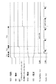
【図7】従来例に係る液晶表示装置の構成の一例を示すブロック図である。
【符号の説明】
11…ガラス基板、12…表示部、13…インターフェース(IF)回路、14…タイミングジェネレータ(TG)、16…水平ドライバ、17…垂直ドライバ、18…CSドライバ、19…VCOMドライバ、22,22′…VCOM調整回路、50…画素、51…TFT(画素トランジスタ)、52…液晶セル、53…保持容量、164…Sig/CS出力切り替え回路[0001]
BACKGROUND OF THE INVENTION
BACKGROUND OF THE INVENTION 1. Field of the Invention The present invention relates to a liquid crystal display device, a control method therefor, and a portable terminal, and more particularly, a drive circuit integrated liquid crystal display device in which a peripheral drive circuit is integrally formed with a display unit on the same transparent insulating substrate, and a power supply thereof The present invention relates to an ON / OFF control method and a portable terminal equipped with the liquid crystal display device as a screen display unit.
[0002]
[Prior art]
In a liquid crystal display device, as a measure to prevent image distortion when the power is turned on (turned on) / off (cut off), white data for normally white type (black data for normally black type) is used as a pixel at power on / off. A configuration is employed in which white display (black display in the normally black type) is performed by writing. Specifically, when the power is turned on, first, white display (or black display) is performed to eliminate image distortion, and then image display according to the display data is performed. When the power is turned off, white display (or black display) is performed. The display is erased after the afterimage is eliminated by performing (display).
[0003]
As described above, when writing white data (or black data), the liquid crystal display device according to the conventional example inputs white data (or black data) from the outside and applies VCOM to the counter electrode of the liquid crystal capacitor of the pixel. A configuration has been adopted in which a driver for setting the CS potential applied to the electrode on the counter electrode side of the potential and the holding capacitor to the “L” level is mounted on the external substrate or the external drive IC.
[0004]
That is, in FIG. 7, a
[0005]
On the
[0006]
The
[0007]
[Problems to be solved by the invention]
As described above, the liquid crystal display device according to the conventional example has a circuit for outputting white data (or black data) between the set and the VCOM in order to prevent image disturbance at power ON / OFF. A circuit for lowering the potential and the CS potential is mounted on the external substrate 105 (or external drive IC). Therefore, the display system requires a process of providing the
[0008]
The present invention has been made in view of the above-mentioned problems, and the object of the present invention is to enable a reduction in the size and cost of the entire system and to start displaying images without any disturbance when the power is turned on. An object of the present invention is to provide a liquid crystal display device capable of erasing display without an afterimage when the power is turned off, a control method thereof, and a portable terminal equipped with the liquid crystal display device as a screen display unit.
[0009]
[Means for Solving the Problems]
The liquid crystal display device according to the present invention includes a display unit in which pixels are arranged in a matrix on a transparent insulating substrate, and a display signal is selected and supplied to each pixel of the display unit. Instead of the display signal Ground level Switching means for selecting and supplying, and a common potential common to each pixel on the counter electrode side of the pixel, and switching to the common potential at power ON / OFF The Ground level Is applied to the counter electrode of the liquid crystal cell of the pixel instead of the common potential. Ground level Alternatively, it is applied to the electrode on the counter electrode side of the storage capacitor instead of the common potential. Ground level The switching means selects the output potential of the potential generating means when the power is turned on / off, and when the power is turned on, the power is first turned on, then the circuit state on the transparent insulating substrate is initialized, and then For each pixel of the display section for a certain period Ground level And write Ground level Is applied to the counter electrode side of the pixel, and when the power is turned off, first for each pixel of the display portion for a certain period of time Ground level And write Ground level Is applied to the counter electrode side of the pixel. Note that the common potential refers to a potential applied to the counter electrode of the liquid crystal cell and a potential applied to the electrode on the counter electrode side of the storage capacitor. This liquid crystal display device is mounted as a screen display unit in a mobile terminal represented by a PDA (Personal Digital Assistants) or a mobile phone.
[0010]
In the liquid crystal display device having the above configuration or a portable terminal equipped with this as a screen display unit, when the power is turned on, the power is first turned on, and then the circuit state on the transparent insulating substrate is initialized. For pixel Ground level And write Ground level By giving to the counter electrode side of the pixel, white display is performed in the normally white type (black display in the normally black type) for a certain period after the power is turned on. As a result, it is possible to start display without image distortion when the power is turned on. In addition, when the power is turned off, first for each pixel of the display portion for a certain period of time. Ground level And write Ground level By giving to the counter electrode side of the pixel, white display (or black display) is performed for a certain period before the power is shut off. Thereby, the display can be erased without an afterimage when the power is turned off.
[0011]
DETAILED DESCRIPTION OF THE INVENTION
Hereinafter, embodiments of the present invention will be described in detail with reference to the drawings.
[0012]
[First Embodiment]
FIG. 1 is a block diagram showing a configuration example of a liquid crystal display device according to the first embodiment of the present invention. In FIG. 1, a display unit (pixel unit) 12 in which pixels are arranged in a matrix is formed on a transparent insulating substrate, for example, a glass substrate 11. The glass substrate 11 is disposed opposite to another glass substrate with a predetermined gap, and a liquid crystal material is sealed between the two substrates to constitute a display panel (LCD panel).
[0013]
An example of the configuration of each pixel in the
[0014]
In this pixel structure, the TFT 51 has a gate electrode connected to a gate line (scanning line) 54 and a source electrode connected to a data line (signal line) 55. The counter electrode of the liquid crystal cell 52 is connected to the VCOM line 56 in common for each pixel. A common voltage VCOM (VCOM potential) is applied to the common electrode of the liquid crystal cell 52 via the VCOM line 56. The other electrode (terminal on the counter electrode side) of the storage capacitor 53 is connected to the CS line 57 in common for each pixel.
[0015]
Here, in the case of performing IH (H is a horizontal period) inversion driving or 1F (F is a field period) inversion driving, the display signal written to each pixel is inverted in polarity with respect to the VCOM potential. When VCOM inversion driving that inverts the polarity of the VCOM potential in the 1H cycle or 1F cycle is used in combination with the IH inversion driving or 1F inversion driving, the polarity of the CS potential applied to the CS line 57 is also inverted in synchronization with the VCOM potential. To do. However, the liquid crystal display device according to the present embodiment is not limited to the VCOM inversion driving. Note that since the VCOM potential and the CS potential are substantially the same potential, in this specification, these are collectively referred to as a common potential.
[0016]
In FIG. 1 again, on the same glass substrate 11 as the
[0017]
In the liquid crystal display device having the above-described configuration, the master clock MCK, the horizontal synchronization pulse Hsync, the vertical synchronization pulse Vsync, R (red) G (green) B with a low voltage amplitude (for example, 3.3 V amplitude) with respect to the glass substrate 11. (Blue) Display data Data of parallel input and display reset control pulse PCI are inputted from the outside via the flexible cable (substrate) 21 and level-shifted (level conversion) to a high voltage amplitude (for example, 6.5 V) in the interface circuit 13 )
[0018]
The level-shifted master clock MCK, horizontal synchronization pulse Hsync, and vertical synchronization pulse Vsync are supplied to the
[0019]
The horizontal driver 16 includes, for example, a
[0020]
The data
[0021]
The analog display signal Sig for one line output from the
[0022]
The
[0023]
When scanning pulses are sequentially output to the gate lines 54-1 to 54-m by the vertical scanning by the
[0024]
The
[0025]
The
[0026]
Here, an AC voltage having substantially the same amplitude as the CS potential is used as the VCOM potential. However, in actuality, in FIG. 2, when a signal is written from the
[0027]
The VCOM adjustment circuit 22 is connected between the capacitor C that receives the VCOM potential, the variable resistor VR connected between the output terminal of the capacitor C and the external power supply VCC1, and the output terminal of the capacitor C and the ground. The DC level of the VCOM potential applied to the counter electrode of the liquid crystal cell 52 is adjusted, that is, a DC offset is applied to the VCOM potential. The
[0028]
In the liquid crystal display device having the above configuration, when the display reset control pulse PCI applied from the outside is at a low level, the
[0029]
With respect to each pixel in the row selected by the vertical scanning by the
[0030]
As described above, in the liquid crystal display device according to the first embodiment, on the same panel (glass substrate 11) as the
[0031]
When a display reset control pulse PCI is applied from the outside, a predetermined potential is written to the pixel, and simultaneously, the CS potential and the VCOM potential are set to the same potential as the pixel potential, and the same potential is applied to the counter electrode side. Therefore, white display is possible with the normally white type, and black display is possible with the normally black type. Therefore, the entire system can be reduced in size and cost, and the image is disturbed when the power is turned on / off. Can be prevented.
[0032]
Next, in the liquid crystal display device having the above-described configuration, a control method for performing a display reset operation in order to prevent image disturbance when the power is turned on / off will be described.
[0033]
First, the display reset operation when the power is turned on will be described with reference to the timing chart of FIG. When turning on the power, first, the power supply VCC1 (eg, 3.3V) and the power supply VDD (eg, 6.5V) are turned on. When a certain period T11 (for example, about 1 msec) elapses after the power supply VCC1 rises about 90%, the master clock MCK, the horizontal synchronization pulse Hsync, the vertical synchronization pulse Vsync, the display data Data, and the display reset control pulse PCI pass through the
[0034]
Thereafter, when a certain period T12 (for example, about 1 msec) elapses, the system reset pulse RST in the panel is set to a high level. As a result, the initial state of a logic circuit such as a flip-flop in the panel is determined (initialized). Thereafter, a low level period of the display reset control pulse PCI is provided for a certain period T13 (for example, 1-2 field periods).
[0035]
In this period T13, the
[0036]
As described above, in the liquid crystal display device, when the power is turned on, the power is first turned on, then the circuit state on the panel is initialized, and then the display reset operation is performed for a certain period of time. By performing display (or black display), it is possible to start display without image distortion when the power is turned on.
[0037]
Next, the display reset operation when the power is turned off will be described with reference to the timing chart of FIG. When the power is turned off, the display reset control pulse PCI is first set to a low level for a certain period T21 (for example, 1-2 field periods). As a result, the
[0038]
That is, white display (or black display) is performed over several field periods by the display reset operation. After the elapse of the period T21, the system reset pulse RST is set to a low level. Thereafter, when a period T22 (for example, about 1 msec) elapses, the master clock MCK, the horizontal synchronization pulse Hsync, the vertical synchronization pulse Vsync, the display data Data, and the display reset control pulse PCI stop the input of the
[0039]
As described above, in the liquid crystal display device, when the power is turned off, the display reset operation is first performed for a certain period of time to perform white display (or black display) for several field periods before the power is shut off, and then the power is shut off. Thus, the display can be erased without an afterimage when the power is turned off.
[0040]
In this control example, the case of preventing image disturbance at power ON / OFF has been described as an example. However, when the liquid crystal display device has a standby mode for the purpose of power saving, for example, the standby mode When entering, the same control as when the power is turned on is performed, and when returning from the standby mode, the same control as when the power is turned off is performed to prevent image disturbance when entering or returning to the standby mode. Can do.
[0041]
[Second Embodiment]
FIG. 5 is a block diagram showing an example of the configuration of a liquid crystal display device according to the second embodiment of the present invention. In FIG. 5, the same parts as those in FIG.
[0042]
In the liquid crystal display device according to the first embodiment, the VCOM adjustment circuit 22 is entirely configured outside the panel (outside of the glass substrate 11), whereas in the liquid crystal display device according to the present embodiment, the VCOM adjustment circuit 22 ′ is provided. A configuration in which part of the circuit elements to be configured is fabricated on the glass substrate 11 is employed.
[0043]
Specifically, in FIG. 5, the capacitor C that is difficult to mount on the glass substrate 11 and the variable resistor VR that requires external adjustment are provided outside the glass substrate 11. The variable resistor VR is connected between the output terminal of the capacitor C and the ground. On the other hand, on the glass substrate 11, a voltage dividing resistor R11 and a switch SW connected in series between the line L electrically connected to the output terminal of the capacitor C and the internal power supply VCC2, and between the line L and the ground. And a voltage dividing resistor R12 connected to the. The switch SW is turned off (opened) when the display reset control pulse PCI output from the
[0044]
By the way, when the VCOM adjustment circuit 22 is entirely configured outside the panel, the display reset control pulse PCI becomes unstable when the power is turned off, and the external power supply VCC1 still remains (at a potential in the vicinity of 3.3 V). Then, the VCOM potential may increase. On the other hand, in the liquid crystal display device according to the present embodiment, a part of the circuit elements constituting the VCOM adjustment circuit 22 ′, specifically, the voltage dividing resistors R11 and R12 and the switch SW for turning on / off them are provided. Since the potential of the line L is pulled to the ground level by turning off the switch SW when the display reset control pulse PCI is at a low level, the rise of the VCOM potential is reliably suppressed. Can be maintained at ground level.
[0045]
In each of the above embodiments, when the display reset control pulse PCI is given, the Sig / CS
[0046]
Further, instead of selecting the CS potential or the VCOM potential, it is possible to select a predetermined potential while setting the CS potential and the VCOM potential to the same potential. Further, the potential (pixel potential) written to the pixel through the data lines 55-1 to 55-n is not limited to 0V (ground level), and the condition for setting the CS potential and the VCOM potential to the same potential as the pixel potential. If the above condition is satisfied, no voltage is applied to the liquid crystal cell 52. Therefore, white display can be performed in the normally white type, and black display can be performed in the normally black type. However, when the pixel potential is set to 0 V, it is not necessary to consume power when writing data to the pixels through the data lines 55-1 to 55-n, which is advantageous from the viewpoint of reducing power consumption.
[0047]
The liquid crystal display device according to the first and second embodiments described above is suitable for use as a screen display unit of a small and light portable terminal typified by a cellular phone or PDA (Personal Digital Assistants). It is.
[0048]
FIG. 6 is an external view showing an outline of the configuration of a portable terminal, for example, a PDA according to the present invention.
[0049]
The PDA according to this example has, for example, a foldable configuration in which a lid 62 is provided to be openable and closable with respect to the apparatus main body 61. On the upper surface of the apparatus main body 61, an operation unit 63 in which various keys such as a keyboard are arranged is arranged. On the other hand, a screen display unit 64 is disposed on the lid 62. As the screen display unit 64, the liquid crystal display device according to the first and second embodiments described above is used.
[0050]
As described above, the liquid crystal display devices according to these embodiments can reduce the size and cost of the entire system, and can prevent image disturbance at power ON / OFF. By mounting the liquid crystal display device as the screen display unit 64, it is possible to greatly contribute to the downsizing of the PDA and to reliably prevent image disturbance when the screen display unit 64 is powered on / off.
[0051]
In addition, a portable terminal represented by this type of PDA generally has a standby mode in order to save power. When entering / returning to the standby mode, as described above, the display reset operation is performed in the same manner as when the power is turned on / off, so that the image disturbance when entering / returning to the standby mode is also possible. It can be surely prevented.
[0052]
Here, the case where the present invention is applied to a PDA has been described as an example. However, the present invention is not limited to this application example, and the liquid crystal display device according to the present invention is particularly applicable to small and light portable terminals such as mobile phones. It is suitable for use.
[0053]
【The invention's effect】
As described above, according to the present invention, a peripheral driving circuit is mounted on the same transparent insulating substrate as the display unit, so that a display panel integrated with all driving circuits can be configured. Since there is no need to provide an IC or transistor circuit, the entire system can be reduced in size and cost. In addition, when the power is turned on / off, a predetermined potential is written to the pixel, and at the same time, the same potential as the predetermined potential is applied to the counter electrode side, so that the white display is normally white and the black display is normally black. Therefore, it is possible to reduce the size and cost of the entire system, and to prevent image disturbance when the power is turned on / off.
[Brief description of the drawings]
FIG. 1 is a block diagram illustrating a configuration example of a liquid crystal display device according to a first embodiment of the present invention.
FIG. 2 is a circuit diagram illustrating an example of a configuration of a pixel.
FIG. 3 is a timing chart for explaining a display reset operation when the power is turned on.
FIG. 4 is a timing chart for explaining a display reset operation when the power is turned off.
FIG. 5 is a block diagram illustrating a configuration example of a liquid crystal display device according to a second embodiment of the present invention.
FIG. 6 is an external view showing a schematic configuration of a PDA according to the present invention.
FIG. 7 is a block diagram illustrating an example of a configuration of a liquid crystal display device according to a conventional example.
[Explanation of symbols]
DESCRIPTION OF SYMBOLS 11 ... Glass substrate, 12 ... Display part, 13 ... Interface (IF) circuit, 14 ... Timing generator (TG), 16 ... Horizontal driver, 17 ... Vertical driver, 18 ... CS driver, 19 ... VCOM driver, 22, 22 ' ... VCOM adjustment circuit, 50 ... pixel, 51 ... TFT (pixel transistor), 52 ... liquid crystal cell, 53 ... holding capacitor, 164 ... Sig / CS output switching circuit
Claims (4)
前記表示部の各画素に対して表示信号を供給するとともに、電源ON/OFF時には前記表示信号に代えてグランドレベルを選択して供給する切り替え手段と、
前記透明絶縁基板上に前記表示部と共に搭載され、前記画素の対向電極側に各画素共通にコモン電位を与えるとともに、電源ON/OFF時には前記コモン電位に代えてグランドレベルを前記画素の対向電極側に与える電位生成手段とを備え、
前記電位生成手段の電源ON/OFF時の出力電位は、前記画素の液晶セルの対向電極に前記コモン電位に代えて与えるグランドレベルまたは保持容量の対向電極側の電極に前記コモン電位に代えて与えるグランドレベルであり、
前記切り替え手段は、電源ON/OFF時には前記電位生成手段の出力電位を選択し、
電源ONに際して、先ず電源を投入し、続いて前記透明絶縁基板上の回路の状態を初期化し、その後一定期間前記表示部の各画素に対してグランドレベルを書き込むとともに、当該グランドレベルを前記画素の対向電極側に与え、
電源OFFに際して、先ず一定期間前記表示部の各画素に対してグランドレベルを書き込むとともに、当該グランドレベルを前記画素の対向電極側に与える
液晶表示装置。A display unit in which pixels are arranged in a matrix on a transparent insulating substrate;
A switching unit that supplies a display signal to each pixel of the display unit, and selects and supplies a ground level instead of the display signal when the power is turned ON / OFF;
Mounted on the transparent insulating substrate together with the display unit, a common potential is applied to each pixel on the counter electrode side, and a ground level is set instead of the common potential when the power is turned on / off. Potential generating means for supplying to
The output potential at the time of power ON / OFF of the potential generating means is applied instead of the common potential to the ground level applied to the counter electrode of the liquid crystal cell of the pixel instead of the common potential or to the electrode on the counter electrode side of the storage capacitor. Ground level,
The switching means selects the output potential of the potential generating means at power ON / OFF,
When turning on the power, first, the power is turned on, then the circuit state on the transparent insulating substrate is initialized, and then the ground level is written to each pixel of the display unit for a certain period, and the ground level is set to the pixel. To the counter electrode side,
A liquid crystal display device that first writes a ground level to each pixel of the display unit for a certain period of time when the power is turned off, and applies the ground level to the counter electrode side of the pixel.
前記電位生成手段の電源ON/OFF時の出力電位は、前記画素の液晶セルの対向電極に前記コモン電位に代えて与えるグランドレベルまたは保持容量の対向電極側の電極に前記コモン電位に代えて与えるグランドレベルである液晶表示装置の駆動に当たって、
電源ONに際して、先ず電源を投入し、続いて前記透明絶縁基板上の回路の状態を初期化し、その後一定期間前記表示部の各画素に対して前記電位生成手段から出力されるグランドレベルを書き込むとともに、当該グランドレベルを前記画素の対向電極側に与え、
電源OFFに際して、先ず一定期間前記表示部の各画素に対して前記電位生成手段から出力されるグランドレベルを書き込むとともに、当該グランドレベルを前記画素の対向電極側に与える
液晶表示装置の制御方法。A display unit in which pixels are arranged in a matrix and a potential generating unit that applies a common potential to each pixel on the counter electrode side of the pixel are mounted on the same transparent insulating substrate,
The output potential at the time of power ON / OFF of the potential generating means is applied instead of the common potential to the ground level applied to the counter electrode of the liquid crystal cell of the pixel instead of the common potential or to the electrode on the counter electrode side of the storage capacitor. In driving a liquid crystal display device at the ground level,
When turning on the power, first, the power is turned on, then the circuit state on the transparent insulating substrate is initialized, and then the ground level output from the potential generating means is written to each pixel of the display section for a certain period of time. , Giving the ground level to the counter electrode side of the pixel,
A method for controlling a liquid crystal display device, wherein when the power is turned off, a ground level output from the potential generating means is first written to each pixel of the display section for a certain period, and the ground level is given to the counter electrode side of the pixel.
前記表示部の各画素に対して表示信号を供給するとともに、電源ON/OFF時には前記表示信号に代えてグランドレベルを選択して供給する切り替え手段と、
前記透明絶縁基板上に前記表示部と共に搭載され、前記画素の対向電極側に各画素共通にコモン電位を与えるとともに、電源ON/OFF時には前記コモン電位に代えてグランドレベルを前記画素の対向電極側に与える電位生成手段とを備え、
前記電位生成手段の電源ON/OFF時の出力電位は、前記画素の液晶セルの対向電極に前記コモン電位に代えて与えるグランドレベルまたは保持容量の対向電極側の電極に前記コモン電位に代えて与えるグランドレベルであり、
前記切り替え手段は、電源ON/OFF時には前記電位生成手段の出力電位を選択し、
電源ONに際して、先ず電源を投入し、続いて前記透明絶縁基板上の回路の状態を初期化し、その後一定期間前記表示部の各画素に対してグランドレベルを書き込むとともに、当該グランドレベルを前記画素の対向電極側に与え、
電源OFFに際して、先ず一定期間前記表示部の各画素に対してグランドレベルを書き込むとともに、当該グランドレベルを前記画素の対向電極側に与える
液晶表示装置を画面表示部として搭載した携帯端末。A display unit in which pixels are arranged in a matrix on a transparent insulating substrate;
A switching unit that supplies a display signal to each pixel of the display unit, and selects and supplies a ground level instead of the display signal when the power is turned ON / OFF;
Mounted on the transparent insulating substrate together with the display unit, a common potential is applied to each pixel on the counter electrode side, and a ground level is set instead of the common potential when the power is turned on / off. Potential generating means for supplying to
The output potential at the time of power ON / OFF of the potential generating means is applied instead of the common potential to the ground level applied to the counter electrode of the liquid crystal cell of the pixel instead of the common potential or to the electrode on the counter electrode side of the storage capacitor. Ground level,
The switching means selects the output potential of the potential generating means at power ON / OFF,
When turning on the power, first, the power is turned on, then the circuit state on the transparent insulating substrate is initialized, and then the ground level is written to each pixel of the display unit for a certain period, and the ground level is set to the pixel. To the counter electrode side,
A portable terminal equipped with a liquid crystal display device as a screen display unit that first writes a ground level to each pixel of the display unit for a certain period of time when the power is turned off and applies the ground level to the counter electrode side of the pixel.
スタンバイモードに入るとき/解除するときに、前記切り替え手段は前記表示部の各画素に対して前記グランドレベルを供給し、前記電位生成手段は前記グランドレベルと同電位を前記画素の対向電極側に与える
請求項3記載の携帯端末。In a mobile terminal having a standby mode,
When entering / releasing the standby mode, the switching unit supplies the ground level to each pixel of the display unit, and the potential generating unit sets the same potential as the ground level to the counter electrode side of the pixel. The mobile terminal according to claim 3.
Priority Applications (8)
| Application Number | Priority Date | Filing Date | Title |
|---|---|---|---|
| JP2002159032A JP4269582B2 (en) | 2002-05-31 | 2002-05-31 | Liquid crystal display device, control method thereof, and portable terminal |
| PCT/JP2003/006857 WO2003102910A1 (en) | 2002-05-31 | 2003-05-30 | Liquid crystal display device, control method thereof, and mobile terminal |
| US10/485,280 US7209132B2 (en) | 2002-05-31 | 2003-05-30 | Liquid crystal display device, method of controlling the same, and mobile terminal |
| CNB03800870XA CN100541588C (en) | 2002-05-31 | 2003-05-30 | Liquid crystal indicator and control method thereof and portable terminal |
| KR1020047001453A KR101074567B1 (en) | 2002-05-31 | 2003-05-30 | Liquid crystal display device, control method thereof, and mobile terminal |
| TW092114789A TWI235267B (en) | 2002-05-31 | 2003-05-30 | Liquid crystal display and its controlling method, and portable terminal |
| US11/789,216 US7796126B2 (en) | 2002-05-31 | 2007-04-23 | Liquid crystal display device, method of controlling the same, and mobile terminal |
| US11/789,279 US7864170B2 (en) | 2002-05-31 | 2007-04-23 | Liquid crystal display device, method of controlling the same, and mobile terminal |
Applications Claiming Priority (1)
| Application Number | Priority Date | Filing Date | Title |
|---|---|---|---|
| JP2002159032A JP4269582B2 (en) | 2002-05-31 | 2002-05-31 | Liquid crystal display device, control method thereof, and portable terminal |
Publications (2)
| Publication Number | Publication Date |
|---|---|
| JP2004004244A JP2004004244A (en) | 2004-01-08 |
| JP4269582B2 true JP4269582B2 (en) | 2009-05-27 |
Family
ID=29706504
Family Applications (1)
| Application Number | Title | Priority Date | Filing Date |
|---|---|---|---|
| JP2002159032A Expired - Fee Related JP4269582B2 (en) | 2002-05-31 | 2002-05-31 | Liquid crystal display device, control method thereof, and portable terminal |
Country Status (6)
| Country | Link |
|---|---|
| US (3) | US7209132B2 (en) |
| JP (1) | JP4269582B2 (en) |
| KR (1) | KR101074567B1 (en) |
| CN (1) | CN100541588C (en) |
| TW (1) | TWI235267B (en) |
| WO (1) | WO2003102910A1 (en) |
Cited By (1)
| Publication number | Priority date | Publication date | Assignee | Title |
|---|---|---|---|---|
| CN105632435A (en) * | 2016-01-05 | 2016-06-01 | 京东方科技集团股份有限公司 | Residual image circuit for switching on/off and method for removing residual image of switching on/off |
Families Citing this family (36)
| Publication number | Priority date | Publication date | Assignee | Title |
|---|---|---|---|---|
| JP4269582B2 (en) * | 2002-05-31 | 2009-05-27 | ソニー株式会社 | Liquid crystal display device, control method thereof, and portable terminal |
| JP4759906B2 (en) * | 2002-12-12 | 2011-08-31 | ソニー株式会社 | Liquid crystal display device, control method thereof, and portable terminal |
| JP4062106B2 (en) * | 2003-01-24 | 2008-03-19 | ソニー株式会社 | Display device |
| JP2005274868A (en) * | 2004-03-24 | 2005-10-06 | Casio Comput Co Ltd | Liquid crystal display device and driving method of liquid crystal display device |
| JP2006047500A (en) * | 2004-08-02 | 2006-02-16 | Seiko Epson Corp | Display panel drive circuit, display device, and electronic apparatus |
| CN100343732C (en) * | 2004-09-16 | 2007-10-17 | 友达光电股份有限公司 | A reference voltage drive circuit with compensation circuit and its compensation method |
| JP4626246B2 (en) * | 2004-09-29 | 2011-02-02 | カシオ計算機株式会社 | Liquid crystal display device and drive control method for liquid crystal display device |
| JP4290627B2 (en) * | 2004-10-04 | 2009-07-08 | シャープ株式会社 | Display element driving apparatus, display device including the display element driving apparatus, and display element driving method |
| JP2006195121A (en) * | 2005-01-13 | 2006-07-27 | Seiko Epson Corp | Electro-optical device, driving method of electro-optical device, and electronic apparatus |
| CN101218623B (en) * | 2005-07-14 | 2010-12-08 | 夏普株式会社 | Active matrix type liquid crystal display device and its drive method |
| WO2007032285A1 (en) * | 2005-09-16 | 2007-03-22 | Sharp Kabushiki Kaisha | Liquid crystal display device |
| US7894848B2 (en) * | 2006-08-31 | 2011-02-22 | Research In Motion Limited | System and method for providing a standby mode in a handheld electronic device |
| CN100547644C (en) * | 2006-10-10 | 2009-10-07 | 奇景光电股份有限公司 | Flat panel display and time schedule controller thereof |
| TWI353575B (en) * | 2006-12-29 | 2011-12-01 | Novatek Microelectronics Corp | Gate driver structure of tft-lcd display |
| KR20080077495A (en) * | 2007-02-20 | 2008-08-25 | 삼성전자주식회사 | Circuit board and liquid crystal display including the same |
| KR101422146B1 (en) * | 2007-08-08 | 2014-07-23 | 삼성디스플레이 주식회사 | Drive device, liquid crystal display device having the same, and driving method of the liquid crystal display device |
| TWI356232B (en) * | 2007-09-28 | 2012-01-11 | Au Optronics Corp | Liquid crystal display for reducing residual image |
| US8791928B2 (en) * | 2007-11-06 | 2014-07-29 | Hannstar Display Corp. | Pixel driving method, pixel driving device and liquid crystal display using thereof |
| TWI379280B (en) | 2007-11-30 | 2012-12-11 | Au Optronics Corp | Liquid crystal display device and method for decaying residual image thereof |
| CN100580761C (en) * | 2007-12-20 | 2010-01-13 | 友达光电股份有限公司 | Liquid crystal display device and method capable of attenuating afterimage thereof |
| JP5481791B2 (en) * | 2008-03-12 | 2014-04-23 | セイコーエプソン株式会社 | Drive circuit, drive method, electro-optical device, and electronic apparatus |
| CN101359445B (en) * | 2008-09-10 | 2013-03-06 | 康佳集团股份有限公司 | System for improving shutdown ghost shadow for plasma TV set |
| TWI418984B (en) * | 2008-12-18 | 2013-12-11 | Wistron Corp | Interface management method and apparatus for a computer system |
| TWI409787B (en) * | 2009-10-30 | 2013-09-21 | Au Optronics Corp | Shift register with image retention release and method for image retention release |
| WO2012137849A1 (en) * | 2011-04-08 | 2012-10-11 | シャープ株式会社 | Display device and method for driving display device |
| TWI434275B (en) * | 2011-09-13 | 2014-04-11 | Au Optronics Corp | Display and dc/dc converter control method |
| US9111500B2 (en) * | 2012-04-19 | 2015-08-18 | Apple Inc. | Devices and methods for pixel discharge before display turn-off |
| GB2504141B (en) * | 2012-07-20 | 2020-01-29 | Flexenable Ltd | Method of reducing artefacts in an electro-optic display by using a null frame |
| WO2014080955A1 (en) * | 2012-11-21 | 2014-05-30 | シャープ株式会社 | Liquid crystal display device |
| JP5827987B2 (en) * | 2013-11-28 | 2015-12-02 | アンリツ株式会社 | Mobile terminal test apparatus and test method |
| KR20160035154A (en) | 2014-09-22 | 2016-03-31 | 삼성디스플레이 주식회사 | Liquid crystal display device and driving method thereof |
| CN104361866A (en) * | 2014-12-02 | 2015-02-18 | 京东方科技集团股份有限公司 | Driving device and driving method of display panel and display device |
| KR101764594B1 (en) | 2015-07-27 | 2017-08-03 | 김익조 | Barley vinegar, and manufacturing method thereof |
| KR20170060980A (en) * | 2015-11-25 | 2017-06-02 | 삼성전자주식회사 | Device for controlling driving frequency and method of operating the same |
| CN108898997B (en) * | 2018-08-31 | 2023-11-28 | 武汉华星光电技术有限公司 | Pixel driving circuit, display panel and display device |
| CN109300446B (en) * | 2018-12-12 | 2022-05-06 | 惠科股份有限公司 | Protection method of display panel, display panel and computer readable storage medium |
Family Cites Families (18)
| Publication number | Priority date | Publication date | Assignee | Title |
|---|---|---|---|---|
| JPS6152683A (en) * | 1984-08-22 | 1986-03-15 | 富士通株式会社 | Power-only-setting circuit for display controller |
| JP2655328B2 (en) * | 1987-12-25 | 1997-09-17 | ホシデン株式会社 | How to clear the LCD display when the power is turned off |
| JPH02272490A (en) * | 1989-04-14 | 1990-11-07 | Hitachi Ltd | Liquid crystal display device and power supply device for liquid crystal display device |
| JP3004710B2 (en) * | 1990-11-28 | 2000-01-31 | 株式会社日立製作所 | Liquid crystal display |
| JPH06118893A (en) * | 1992-10-08 | 1994-04-28 | Jeco Co Ltd | Display apparatus |
| JP3189021B2 (en) * | 1993-06-29 | 2001-07-16 | アンリツ株式会社 | Liquid crystal drive |
| JPH11202842A (en) * | 1998-01-16 | 1999-07-30 | Nec Home Electron Ltd | Liquid crystal display device |
| JPH11271707A (en) * | 1998-03-19 | 1999-10-08 | Toshiba Corp | Liquid crystal display device |
| US6639590B2 (en) * | 1998-04-16 | 2003-10-28 | Seiko Epson Corporation | Method for controlling liquid crystal display device, device for driving liquid crystal display device, liquid crystal display device, and electronic apparatus |
| JP3796070B2 (en) * | 1999-07-21 | 2006-07-12 | シャープ株式会社 | Liquid crystal display |
| JP2001209355A (en) * | 2000-01-25 | 2001-08-03 | Nec Corp | Liquid crystal display device and its driving method |
| EP1962262A3 (en) * | 2000-03-30 | 2010-03-17 | Seiko Epson Corporation | Display device with data memory capability |
| JP3992984B2 (en) | 2002-01-04 | 2007-10-17 | シャープ株式会社 | LCD panel |
| JP3868826B2 (en) | 2002-02-25 | 2007-01-17 | シャープ株式会社 | Image display apparatus driving method and image display apparatus driving apparatus |
| US7698573B2 (en) * | 2002-04-02 | 2010-04-13 | Sharp Corporation | Power source apparatus for display and image display apparatus |
| JP4269582B2 (en) * | 2002-05-31 | 2009-05-27 | ソニー株式会社 | Liquid crystal display device, control method thereof, and portable terminal |
| JP3741079B2 (en) * | 2002-05-31 | 2006-02-01 | ソニー株式会社 | Display device and portable terminal |
| KR100936188B1 (en) | 2003-05-26 | 2010-01-11 | 삼성전자주식회사 | Liquid crystal display and its driving method and apparatus |
-
2002
- 2002-05-31 JP JP2002159032A patent/JP4269582B2/en not_active Expired - Fee Related
-
2003
- 2003-05-30 KR KR1020047001453A patent/KR101074567B1/en active IP Right Grant
- 2003-05-30 TW TW092114789A patent/TWI235267B/en not_active IP Right Cessation
- 2003-05-30 US US10/485,280 patent/US7209132B2/en not_active Expired - Lifetime
- 2003-05-30 WO PCT/JP2003/006857 patent/WO2003102910A1/en active Application Filing
- 2003-05-30 CN CNB03800870XA patent/CN100541588C/en not_active Expired - Fee Related
-
2007
- 2007-04-23 US US11/789,216 patent/US7796126B2/en active Active
- 2007-04-23 US US11/789,279 patent/US7864170B2/en active Active
Cited By (2)
| Publication number | Priority date | Publication date | Assignee | Title |
|---|---|---|---|---|
| CN105632435A (en) * | 2016-01-05 | 2016-06-01 | 京东方科技集团股份有限公司 | Residual image circuit for switching on/off and method for removing residual image of switching on/off |
| CN105632435B (en) * | 2016-01-05 | 2018-06-05 | 京东方科技集团股份有限公司 | Switching on and shutting down image retention eliminates circuit and the method for eliminating switching on and shutting down image retention |
Also Published As
| Publication number | Publication date |
|---|---|
| CN1547730A (en) | 2004-11-17 |
| CN100541588C (en) | 2009-09-16 |
| US20040196278A1 (en) | 2004-10-07 |
| US7209132B2 (en) | 2007-04-24 |
| KR20050008630A (en) | 2005-01-21 |
| US20070195037A1 (en) | 2007-08-23 |
| WO2003102910A1 (en) | 2003-12-11 |
| KR101074567B1 (en) | 2011-10-17 |
| US7796126B2 (en) | 2010-09-14 |
| JP2004004244A (en) | 2004-01-08 |
| TWI235267B (en) | 2005-07-01 |
| US7864170B2 (en) | 2011-01-04 |
| TW200407599A (en) | 2004-05-16 |
| US20070195038A1 (en) | 2007-08-23 |
Similar Documents
| Publication | Publication Date | Title |
|---|---|---|
| JP4269582B2 (en) | Liquid crystal display device, control method thereof, and portable terminal | |
| JP5019668B2 (en) | Display device and control method thereof | |
| JP3741079B2 (en) | Display device and portable terminal | |
| JP4158658B2 (en) | Display driver and electro-optical device | |
| US7692615B2 (en) | Display driver, electro-optical device, and method of driving electro-optical device | |
| US7932901B2 (en) | Timing generating circuit, display apparatus, and portable terminal | |
| US7079096B2 (en) | Image display device and display driving method | |
| JP4868652B2 (en) | Display device | |
| JP2001166741A (en) | Semiconductor integrated circuit device and liquid crystal display device | |
| JP2002350808A (en) | Driving circuit and display device | |
| JP4759906B2 (en) | Liquid crystal display device, control method thereof, and portable terminal | |
| JP4110839B2 (en) | Display device and portable terminal | |
| JP2008225494A (en) | Display driver and electro-optical device | |
| US20070146286A1 (en) | Apparatus and method for driving LCD | |
| JP4082282B2 (en) | Liquid crystal display device and portable terminal | |
| TW548466B (en) | Display device | |
| JP3443059B2 (en) | Afterimage erasing method and display device using the afterimage erasing method | |
| JP2004226435A (en) | Display device and mobile terminal | |
| US20240404486A1 (en) | Liquid crystal display device and method of driving the same | |
| US20240404485A1 (en) | Liquid crystal display device and method of driving the same | |
| JP2009294426A (en) | Display apparatus |
Legal Events
| Date | Code | Title | Description |
|---|---|---|---|
| A621 | Written request for application examination |
Free format text: JAPANESE INTERMEDIATE CODE: A621 Effective date: 20040427 |
|
| A131 | Notification of reasons for refusal |
Free format text: JAPANESE INTERMEDIATE CODE: A131 Effective date: 20071127 |
|
| A521 | Request for written amendment filed |
Free format text: JAPANESE INTERMEDIATE CODE: A523 Effective date: 20080125 |
|
| A02 | Decision of refusal |
Free format text: JAPANESE INTERMEDIATE CODE: A02 Effective date: 20080325 |
|
| A521 | Request for written amendment filed |
Free format text: JAPANESE INTERMEDIATE CODE: A523 Effective date: 20080523 |
|
| A911 | Transfer to examiner for re-examination before appeal (zenchi) |
Free format text: JAPANESE INTERMEDIATE CODE: A911 Effective date: 20080530 |
|
| A131 | Notification of reasons for refusal |
Free format text: JAPANESE INTERMEDIATE CODE: A131 Effective date: 20081125 |
|
| A521 | Request for written amendment filed |
Free format text: JAPANESE INTERMEDIATE CODE: A523 Effective date: 20081225 |
|
| TRDD | Decision of grant or rejection written | ||
| A01 | Written decision to grant a patent or to grant a registration (utility model) |
Free format text: JAPANESE INTERMEDIATE CODE: A01 Effective date: 20090203 |
|
| A01 | Written decision to grant a patent or to grant a registration (utility model) |
Free format text: JAPANESE INTERMEDIATE CODE: A01 |
|
| A61 | First payment of annual fees (during grant procedure) |
Free format text: JAPANESE INTERMEDIATE CODE: A61 Effective date: 20090216 |
|
| FPAY | Renewal fee payment (event date is renewal date of database) |
Free format text: PAYMENT UNTIL: 20120306 Year of fee payment: 3 |
|
| R151 | Written notification of patent or utility model registration |
Ref document number: 4269582 Country of ref document: JP Free format text: JAPANESE INTERMEDIATE CODE: R151 |
|
| FPAY | Renewal fee payment (event date is renewal date of database) |
Free format text: PAYMENT UNTIL: 20120306 Year of fee payment: 3 |
|
| FPAY | Renewal fee payment (event date is renewal date of database) |
Free format text: PAYMENT UNTIL: 20120306 Year of fee payment: 3 |
|
| FPAY | Renewal fee payment (event date is renewal date of database) |
Free format text: PAYMENT UNTIL: 20130306 Year of fee payment: 4 |
|
| R250 | Receipt of annual fees |
Free format text: JAPANESE INTERMEDIATE CODE: R250 |
|
| FPAY | Renewal fee payment (event date is renewal date of database) |
Free format text: PAYMENT UNTIL: 20130306 Year of fee payment: 4 |
|
| S111 | Request for change of ownership or part of ownership |
Free format text: JAPANESE INTERMEDIATE CODE: R313113 |
|
| FPAY | Renewal fee payment (event date is renewal date of database) |
Free format text: PAYMENT UNTIL: 20130306 Year of fee payment: 4 |
|
| R350 | Written notification of registration of transfer |
Free format text: JAPANESE INTERMEDIATE CODE: R350 |
|
| FPAY | Renewal fee payment (event date is renewal date of database) |
Free format text: PAYMENT UNTIL: 20130306 Year of fee payment: 4 |
|
| FPAY | Renewal fee payment (event date is renewal date of database) |
Free format text: PAYMENT UNTIL: 20140306 Year of fee payment: 5 |
|
| R250 | Receipt of annual fees |
Free format text: JAPANESE INTERMEDIATE CODE: R250 |
|
| R250 | Receipt of annual fees |
Free format text: JAPANESE INTERMEDIATE CODE: R250 |
|
| R250 | Receipt of annual fees |
Free format text: JAPANESE INTERMEDIATE CODE: R250 |
|
| R250 | Receipt of annual fees |
Free format text: JAPANESE INTERMEDIATE CODE: R250 |
|
| R250 | Receipt of annual fees |
Free format text: JAPANESE INTERMEDIATE CODE: R250 |
|
| R250 | Receipt of annual fees |
Free format text: JAPANESE INTERMEDIATE CODE: R250 |
|
| R250 | Receipt of annual fees |
Free format text: JAPANESE INTERMEDIATE CODE: R250 |
|
| R250 | Receipt of annual fees |
Free format text: JAPANESE INTERMEDIATE CODE: R250 |
|
| R250 | Receipt of annual fees |
Free format text: JAPANESE INTERMEDIATE CODE: R250 |
|
| S111 | Request for change of ownership or part of ownership |
Free format text: JAPANESE INTERMEDIATE CODE: R313111 |
|
| R350 | Written notification of registration of transfer |
Free format text: JAPANESE INTERMEDIATE CODE: R350 |
|
| LAPS | Cancellation because of no payment of annual fees |