JP3641929B2 - Manufacturing method of semiconductor device - Google Patents
Manufacturing method of semiconductor device Download PDFInfo
- Publication number
- JP3641929B2 JP3641929B2 JP05654398A JP5654398A JP3641929B2 JP 3641929 B2 JP3641929 B2 JP 3641929B2 JP 05654398 A JP05654398 A JP 05654398A JP 5654398 A JP5654398 A JP 5654398A JP 3641929 B2 JP3641929 B2 JP 3641929B2
- Authority
- JP
- Japan
- Prior art keywords
- oxide film
- impurity
- single crystal
- polycrystalline silicon
- crystal silicon
- Prior art date
- Legal status (The legal status is an assumption and is not a legal conclusion. Google has not performed a legal analysis and makes no representation as to the accuracy of the status listed.)
- Expired - Fee Related
Links
Images


Landscapes
- Formation Of Insulating Films (AREA)
Description
【0001】
【発明の属する技術分野】
本発明は半導体素子、特にトレンチ構造を用いるUMOS等に代表される縦形トランジスタの電極形成法に関するものである。
【0002】
【従来の技術】
近年、電力用半導体素子においては、高性能化のため半導体基板の表面から溝を形成し、その側面をチャネルとして利用するUMOSと称される構造を代表とする素子が実用化されつつある。本出願人は、これと類似の構造を用いるも全く新しい動作機構による電力用素子を発明し、既に出願している(特開平6−252408号)。
【0003】
図18は、上記電力用素子の概略構造を示す断面斜視図である。図18において、基板21上に形成したドレイン領域22の表面に、同じ導電型のソース領域23を設け、ドレイン領域22の一部と上記ソース領域23とを挾み込むようにU字型の固定電位絶縁電極26を配置する。この固定電位絶縁電極26は基板表面から形成した溝(トレンチ)の内表面に設けた絶縁膜25の内側に多結晶シリコン等を充填してMOS型電極24を形成したものであり、ソース電極Sと同電位に保たれていて(すなわち電位が固定されている)、かつ隣接するドレイン領域22に空乏層を形成する材料から成る。そしてこの空乏層によってソース領域23とドレイン領域22は電気的に遮断されるように配設する。上記の溝と溝の間、すなわち各固定電位絶縁電極相互間はチャネル領域27となる。さらに、ドレイン領域22と固定電位絶縁電極26の絶縁膜25とに接し、ソース領域23には接しない反対導電型のゲート領域28を設け、それに外部から任意に電位を設定できるようにしたものである。すなわち、このゲート領域28の電位によって絶縁膜25界面の電位を操作したり、ドレイン領域22の伝導度を制御するものである。その他、29はドレイン電極である。なお、上記の符号や名称などについては原文とは適宜変更して表示している。
【0004】
上記の素子を形成する場合には、ソース領域23はトレンチとトレンチの間の表面に形成する必要がある。そのため、上記従来技術においては、トレンチを形成する工程の前にソース領域形成用の不純物を導入しておき、その後のゲート酸化膜形成(熱酸化によって上記の絶縁膜25を形成する)その他の熱処理において活性化させる手法を用いている。
【0005】
【発明が解決しようとする課題】
上記の素子ではトレンチの間隔を狭め、かつトレンチ深さを浅くする程、素子の電流増幅率が向上する特性を有する。そのため、デザインルールを縮小したマスクで製造することが望ましい。しかし、上記のようにトレンチを形成する工程の前にソース領域形成用の不純物を導入しておき、その後のゲート酸化その他の熱処理において活性化させる手法を用いる方法、すなわち、不純物を拡散した後にトレンチ内壁に酸化膜を形成する方法では、ソース領域がトレンチに挟まれているため、ゲート酸化膜の形成時の酸素増速拡散効果が特に顕著となって、ソース領域の拡散長が非常に大きくなる。すなわち、酸化膜形成時に酸素が拡散し、不純物層の深さが深くなる。なお、酸素増速拡散効果に関しては、例えば、「松本智 他、“酸化雰囲気におけるシリコン中のAs、P、B拡散の時間依存性の解析”半導体・集積回路技術シンポジウム講演論文集、Vol22th、pp72〜77、1982」に記載されている。
【0006】
図19は、上記の現象を説明するための要部断面図であり、1は単結晶シリコン基板、2はトレンチ、3は二酸化シリコン(酸化膜)、16は増速拡散したソース拡散層である。図19に示すように、ソース拡散層16が深くなると、トレンチの有効深さはAからBへと浅くなる。そのため、素子の耐圧を維持するためにはトレンチ2を深く設定する必要性が生じるが、これは前記のように電流増幅率の向上を阻害する要因となるので、性能向上が阻害される。
【0007】
上記の問題を回避するためには、まず、トレンチを形成し、MOS型電極とするための多結晶シリコンを埋め込んだ後に、ソース領域を形成する部分に不純物を導入する必要がある。その方法としては、図20に示すように、レジストマスク19を形成してイオン注入(例えば燐イオン)を行なう方法が考えられる。しかし、微細化するほどパターンのマスク合わせが難しくなり、図20に示すようにマスクずれが生じた場合には、トレンチ内のホウ素がドーピングされた多結晶シリコン4に燐イオンが注入(燐イオン注入拡散層領域17)され、電気抵抗の悪化を招いて素子の遮断特性が劣化したり、ソース領域部のマスクずれ個所にイオンの未注入部分18が残るため、ショットキーコンタクトが形成されることによる電流増幅率低下やオン抵抗の上昇を招き、結果的に歩留の低下を引き起こすという問題があった。
【0008】
本発明は、上記のごとき従来技術の問題点を解決するためになされたものであり、更なる微細化に対応する安定した半導体装置の製造方法を提供することを目的とする。
【0009】
【課題を解決するための手段】
上記の目的を達成するため、本発明においては特許請求の範囲に記載するように構成している。すなわち、請求項1に記載の発明においては、単結晶シリコン基体に設けた溝内に不純物を注入した多結晶シリコンを充填した構造において、単結晶シリコンと不純物を注入した多結晶シリコンとで酸化膜形成速度の異なる温度下で酸化することにより、単結晶シリコン基体の主面に薄い第1の酸化膜を、多結晶シリコンの表面に厚い第2の酸化膜を形成し、厚い第2の酸化膜は通過せず、薄い第1の酸化膜は通過する条件で主面側から不純物注入を行なうことにより、単結晶シリコン基体の主面における溝の周辺部分に不純物層を形成するものである。
【0010】
上記のように、酸化膜形成速度の異なる温度(例えば請求項8に記載のように700〜900℃程度の低温度)下で酸化することにより、単結晶シリコン基体の主面には薄い酸化膜を、多結晶シリコンの表面には厚い酸化膜を自動的に形成することが出来る。したがって薄い酸化膜は通過し、厚い酸化膜は通過しない条件で不純物を注入すれば、薄い酸化膜の部分、すなわち溝の周辺部分にのみ選択的に不純物層(例えばソース領域となる)を形成することが出来る。このようにすれば、溝内面の酸化膜形成後に不純物注入を行なうので、従来のように、酸素増速拡散効果によって不純物層が深くなってしまうという問題を生じることがなく、また、厚い第2の酸化膜は多結晶シリコンの表面にのみ形成されるので、マスクずれによる問題を生じることもなくなる。
【0011】
次に、請求項2に記載の発明は、請求項1に記載の発明のより具体的な製造工程を示すものであり、溝の形成に用いた誘電体マスク(第1の誘電体膜)をそのまま用いて、溝内に形成した多結晶シリコン表面にのみ高濃度拡散層を形成した後、上記誘電体マスクを除去し、前記の低温酸化を行なって薄い第1の酸化膜と厚い第2の酸化膜とを形成し、その膜厚差を利用して必要個所(例えばソース領域)にのみイオン注入を行なうように構成したものである。なお、請求項1または請求項2に記載の構成は、例えば後記図1〜図11に示す第1の実施の形態に相当する。
【0012】
また、請求項3に記載の発明は、請求項2において、多結晶シリコン表面から第2の不純物を拡散する深さT1と、多結晶シリコン表面に形成する第2の酸化膜の膜厚T2との関係について規定するものであり、第1の不純物がホウ素の場合と燐の場合、第2の不純物がホウ素の場合と燐の場合の各組合せによって異なった関係となる。
【0013】
また、請求項4に記載の発明は、請求項2において、第3の不純物を拡散する方法とそのエネルギー条件を規定するものであり、請求項4に記載のように設定することにより、不純物が第1の酸化膜は通過し、第2の酸化膜は通過しないようにすることが出来る。
【0014】
また、請求項5に記載の発明は、第1の誘電体膜の膜厚T3と第2の酸化膜の膜厚T2との関係を規定するものであり、T3≧T2に設定することにより、酸化膜除去後に多結晶シリコンの突出部分による凹凸を少なくし、平坦性をよくすることが出来る。
なお、上記請求項3乃至請求項5に記載の内容は、後記第1の実施の形態中に記載されている。
【0015】
また、請求項6に記載の発明は、請求項1に記載の発明における低温酸化と不純物注入との順序を逆にしたものであり、不純物注入を行なった後に、低温酸化で薄い酸化膜と厚い酸化膜とを形成し、多結晶シリコンにおける不純物層は厚い酸化膜中に全て取り込み、薄い酸化膜の下にのみ不純物層を残すように構成したものである。このように構成することにより、製造工程をより簡単化することが出来る。
【0016】
また、請求項7に記載の発明は、請求項6に記載の発明のより具体的な製造工程を示すものである。なお、請求項6または請求項7に記載の発明は、例えば、後記図12乃至図14に示す第2の実施の形態に相当する。
【0017】
また、請求項8に記載の発明は、請求項1、請求項2、請求項6または請求項7において、単結晶シリコンと不純物を注入した多結晶シリコンとで酸化膜形成速度の異なる温度として、700℃〜900℃の範囲の値を用いたものである。なお、上記の値は後記図17および第1の実施の形態に記載されている。
【0018】
【発明の効果】
本発明の製造方法によれば、溝内面の酸化膜形成後に不純物注入を行なうので、従来のように、酸素増速拡散効果によって不純物層が深くなってしまうという問題を生じることがなく、また、厚い第2の酸化膜は多結晶シリコンの表面にのみ形成されるので、マスクずれによる問題を生じることもなくなるという効果が得られる。また、一連の工程が全てレジストマスク不要のセルフアライン工程となるため、レジスト工程に付随する合わせズレから解放されされて歩留の向上が図られるのみならず、素子の性能向上のためには、溝パターンの微細化のみを考慮すればよいため、更なる微細化が著しく容易となる。
【0019】
【発明の実施の形態】
(第1の実施の形態)
図1〜図11は、本発明の第1の実施の形態における各工程を示す断面図であり、本発明を上記従来例(特開平6−252408号)の構造を形成する場合に適用した例を示す。なお、各図は工程の説明を容易にするためにデフォルメされており、正確な寸法比を示さない部分がある。また、実施の形態中の数値は本実施の形態を説明するための一例であり、これに限定されるものでは無く、外部条件の変動により当然変化するものである。
【0020】
まず、図1は本発明の製造方法による構造が形成された結果を示す断面図であり、単結晶シリコン基板1上にソース領域用の拡散層7が形成されている。単結晶シリコン基板1にはトレンチ2の内表面に二酸化シリコン膜(絶縁膜)3が形成され、そのトレンチ内部に多結晶シリコン4(MOS型電極となる)が埋め込まれている。多結晶シリコン4の上部表面には厚い二酸化シリコン膜5が形成されている。また、薄い二酸化シリコン膜6が形成されている部分がソース電極となる領域で、その下には上記のようにソース拡散層7が形成されている。以下、この構造が形成されるまでを中心に工程の詳細を説明する。なお、上記従来例(特開平6−252408号)の製造に関して、図2に示す形状以前の工程は本発明とは独立の関係にあるため説明を割愛する。
【0021】
図2において、単結晶シリコン基板1上にはトレンチエッチング時のマスクとなる二酸化シリコンを主成分とするPSG膜(誘電体膜)8を形成し、被トレンチエッチング領域9を開孔する。PSG膜8の厚さT3は400nm、PSG濃度は4mol%とした。
【0022】
次に、図3に示すように、トレンチエッチングを施してトレンチ2を形成する。本実施の形態では、トレンチエッチングとして、水素化臭素(HBr)、三弗化窒素(NF3)、酸素(O2)およびヘリウム(He)の混合ガスを導入し、13.56MHzの高周波電力を回転磁界中で印加するマグネトロン・プラズマ増速リアクティブ・イオン・エッチング(MERIE)法を用いて、深さ4μmのトレンチ2を形成した。
【0023】
次に、図4に示すように、トレンチ2の内面に950℃のドライ酸化によって厚さ100nmの二酸化シリコン膜3をゲート酸化膜として形成した。
【0024】
次に、図5に示すように、第1の不純物としてホウ素をドーピングしながら減圧化学的気相成長法を用いて、多結晶シリコン10を厚く形成すると、その形成時の広く知られた良好な被覆特性により表面はほぼ平坦化される。
【0025】
次に、図6に示すように、多結晶シリコン10をHBr、塩素(C12)の混合ガスを用いて、トレンチエッチング時と同様のMERIE法によってエッチバックすることにより、トレンチ2の内部にのみ、埋め込まれた多結晶シリコン4を残す。
【0026】
次に、図7に示すように、多結晶シリコン4の表面に第2の不純物をドーピングして高濃度ドーピング層11を形成する。本発明は低温酸化における高濃度ドーピング層11における酸化膜厚が単結晶シリコンにおける酸化膜厚より厚くなる現象(詳細後述)を利用するものであり、これが製造方法のポイントの一つである。この多結晶シリコン4表面への高濃度ドーピングは、例えば第2の不純物としてホウ素をエネルギー33KeVにて2×1015cm~2イオン注入した後、窒素中にて900℃、20分の活性化を行なうことによって実施し、厚さT1がおよそ300nmの拡散層とした。
【0027】
この高濃度ドーピング層11の形成においては、用いる第2の不純物はホウ素と燐の何れでも良いが、ホウ素の場合には上記の方法の他にBBr3デポジションと呼ばれる不純物拡散による方法でもよい。また第2の不純物が燐の場合には燐のイオン注入法を用いてもよいし、POC13デポジションと呼ばれる不純物拡散による方法でも良い。
【0028】
次に、図8に示すように、弗化水素酸を主成分とするエッチング液に浸漬し、トレンチエッチングマスクおよびドーピングマスクの両用に用いたPSG膜8を除去する。図8はPSG膜8を除去した後の形状を示す。
【0029】
次に、図9に示すように、低温酸化により、高濃度ドーピング層11を酸化した厚い二酸化シリコン膜5(厚さT2)と単結晶シリコン基板1の表面を酸化した薄い酸化膜6(厚さT4)を形成する。
【0030】
ここで、不純物を高濃度にドーピングした多結晶シリコンと単結晶シリコンとにおいて、低温酸化時の酸化膜厚が異なる現象について説明する。
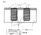
図17は、一定時間の酸化における温度と酸化膜厚との関係の一例を示す特性図である。図17において、一点鎖線Aは単結晶シリコンの特性、実線Bはホウ素(B)を高濃度にドーピングした多結晶シリコンの特性、破線Cは燐(P)を高濃度にドーピングした多結晶シリコンの特性を示す。
【0031】
図17に示すように、一般に広く用いられる900℃以上の酸化温度から低温にして行くに従って、単結晶シリコンの酸化膜厚T4に比較してホウ素や燐を高濃度にドーピングした多結晶シリコンの酸化膜厚(T2)が厚くなる傾向が顕著になることが判った。例えば750℃の場合には、膜厚がホウ素ではT2/T4=2.7倍、燐ではT2/T4=5.6倍となるデータが得られている。
【0032】
従来から一般的に用いられている900℃以上の酸化温度では、単結晶シリコンと高濃度多結晶シリコンとの酸化速度の差が小さくなる。そして700℃付近を下回ると、形成する酸化膜厚にもよるが常識的なレベルを超える異常に長い酸化時間が必要となってくる。したがって本実施の形態のように、T2とT4の差を大きくし、かつ酸化時間が異常に長くならないようにするためには、温度範囲を700℃以上かつ900℃未満とするのが良い。そのため本実施の形態では、ホウ素による酸化であるので、ウェット酸化法にて750℃で923分間酸化して、多結晶シリコン4上に厚さ100nmの二酸化シリコン膜5を形成し、単結晶シリコン1の表面に厚さ37nmの二酸化シリコン膜6を形成した。
【0033】
なお、高濃度ドーピング層11を、第2の不純物としてホウ素を用いたBBr3デポジションによって形成すると、拡散深さ(T1)の管理は緩くなる。本実施の形態のように、多結晶シリコン4に予め第1の不純物としてホウ素がドーピングされ、かつ表面では金属配線と電気的接続(コンタクト)をとる構造の場合には、実質的に問題は生じない。そして工程は簡略化され、必要な酸化膜厚も厚くする必要がなくなる。
【0034】
また、酸化膜厚は一般的に形成に消費した元のシリコン膜厚の5/2になることが知られているから、高濃度ドーピング層11の厚さT1と低温酸化後の酸化膜厚T2との関係を、T1×5/2>T2となるように設定することにより、高濃度ドーピング層11の底部に酸化されない残留領域を残すことが出来る。この残留領域は、後にコンタクトを形成する場合に、コンタクトのための高濃度拡散層の役割を果たすので、さらに工程の簡略化が図られる。
【0035】
一方、高濃度ドーピング層11を形成する際の第2の不純物として、ホウ素よりも酸化速度の大きい不純物である燐をドーピングした場合には、低温酸化における多結晶シリコン4上の酸化膜厚T2と単結晶シリコン上の酸化膜厚T4との差がより大きくなる。そのため高濃度ドーピング層11の厚さT1と低温酸化後の酸化膜厚T2との関係を、T1×5/2≦T2となるように設定することにより、厚めの酸化を行なう場合でも、酸化レートがより大きいので、酸化時間を短く出来るという利点がある。そしてこのような厚めの酸化を行なうことにより、酸化後に電気特性を変化させないようにすることができる。
上記のように、これらの工程の何れをも選択が可能である。
【0036】
逆に、埋め込み多結晶シリコン4に第1の不純物として燐がドープされている場合には、電気的特性への影響排除の観点から、高濃度ドーピング層11の第2の不純物が燐の場合はT1×5/2>T2、上記第2の不純物がホウ素ではT1×5/2≦T2とする必要があることが判る。
【0037】
次に、図10に示すように、上記の2種類の膜厚T2とT4の差を利用してソース領域形成のためのイオン注入を行なう。この場合、多結晶シリコン4内には注入イオンが到達せずにそのほとんどが厚い酸化膜5内に留まるようにし、かつ薄い酸化膜6下の単結晶シリコン1内には注入イオンを到達させる必要がある。そのため、イオン注入条件における注入不純物の平均投影飛程Rpと標準偏差△Rpとの関係を、注入イオンの99%が厚さT2内に収まるようにするため、
Rp+(3×△Rp)<T2
および
Rp>T4
の関係を満たすように注入エネルギーを設定(例えば注入エネルギーを34keVにするとRp=0.0419、△Rp=0.0184になる)すると、図10に示すように、単結晶シリコン1内にのみ不純物が導入され、不純物層14が形成される。
【0038】
その後、本実施の形態では950℃の窒素雰囲気にて20分の活性化アニールを施した後、コンタクト部分の酸化膜5および酸化膜6を除去し、配線層(アルミニウム膜)15を形成すると、図11に示すような構造が形成される。図11の構造は、上記従来例(特開平6−252408号)の基本的構造部分であり、7はソース拡散層(不純物層14に相当)である。なお、前記図18に示したごとく、上記従来例の構造では、MOS型電極24とソース領域23とが共通にソース電極に接続されるので、図11では配線層15が表面全体に形成されているが、別個の電極に接続する場合には、それぞれの電極を形成するようにエッチングすれば良い。
【0039】
なお、配線層15のようなコンタクト形成のためには表面の凹凸が少ないことが望ましい。そのためには、トレンチ2形成のマスクとなり、かつ多結晶シリコン4の表面からの突出高さを決定するPSG膜8の厚さT3を、高濃度ドーピング層11の酸化膜厚T2と比較して、T3≧T2に設定しておくとよい。このように設定するだけで表面の凹凸は大きく改善される。
【0040】
(第2の実施の形態)
次に、図12〜図14は、本発明の第2の実施の形態における工程を示す断面図である。この実施の形態は、前記第1の実施の形態を更に簡略化した工程である。なお、前記図1〜図6に示した多結晶シリコン4形成までの工程は、第1の実施の形態と同一なので説明を省略する。
【0041】
まず、前記図6の工程の次に、図12に示すように、PSG膜8を除去する。
次に、図13に示すように、まず第2の不純物のイオン注入を行なう。この場合には、図示のごとくイオン注入層14が深い位置に形成されるように高エネルギーでイオン注入を行なう。ただし、後に行なう低温酸化工程(高温の酸化に比較して長時間を要する)を考慮すると、酸化膜厚は薄い方が望ましい。そのためには、注入エネルギーは、極力小さい方が好ましいので、エネルギーを40keVとして燐を2×105cm~2だけイオン注入し、イオン注入層14を形成する。この際には、単結晶シリコン1の表面部分と多結晶シリコン4の表面との両方にイオンが注入される。
【0042】
次に、図14に示すように、第1の実施の形態と同様に低温酸化を行なう。この際に形成される酸化膜厚は、多結晶シリコン4の表面にイオン注入された第2の不純物が全て酸化膜内に取り込まれる厚さにする必要がある。
上記の関係は、イオン注入層の厚さT1と低温酸化後の酸化膜厚T2との関係が、T1×5/2≦T2となるから、これを満たすように本実施の形態では前記のように40keVで燐をイオン注入した。その結果、イオン注入層14の深さT1は、T1=Rp+(3×△Rp)≒112nmとなった。
【0043】
また、酸化は燐を用いた場合であるので、750℃のウェット酸化法にて193分間酸化し、厚さ150nmの多結晶シリコンの酸化膜5を形成した。このとき単結晶シリコン側における酸化膜6の厚さは26nm程度であり、イオン注入時のRp=48.6nmに対しての表面側高濃度範囲であるRp−△Rp=18.8nmの範囲には僅かしか入り込まない。したがって、単結晶シリコン側における燐のイオン注入層14の多くは酸化されずに残るので、ソース電極拡散層形成のために利用できる。なお、ボロンや燐等の不純物の拡散定数は、酸素原子のそれよりも4桁程度小さいので、拡散による上記関係の崩れを考慮する必要はない。その後、950℃の窒素雰囲気にて20分の活性化アニールを行い、前記図10に示したものと同様の構造が形成される。その後の工程は前記図11と同じである。
【0044】
本実施の形態においては、使用不純物の制限はあるが、第1の実施の形態と同じ効果を持ちながら、より工程を簡略化することが出来る。
【0045】
(第3の実施の形態)
次に、図15、図16は本発明の第3の実施の形態における製造工程を示す断面図である。
前記のように、第1、第2の実施の形態においては、特開平6−252408号に記載の素子の製造に際して本発明を適用する場合について説明したが、本発明は上記の素子の製造に限定されるわけではない。第3の実施の形態は、他のデバイスとして、UMOSデバイス(例えば特開平4−145628号公報に記載の素子)に本発明を適用した場合を説明する。
【0046】
まず、図15に示すように、トレンチの側壁の酸化膜3に接して、単結晶シリコン基板1とは反対の導電型の拡散層13(チャネルになる部分)が形成され、トレンチ内には多結晶シリコン4が充填されている。この図15においても前記第1および第2の実施の形態と同様に、多結晶シリコン4の表面に高濃度に不純物をドーピングし、比較的低温で酸化する工程を用いることにより、前記図7を用いて説明したと同様に2種類の膜厚の酸化膜5、6が表面に形成された構造を形成することが出来る。
【0047】
その後、前記実施の形態と同様にイオン注入を行ってソース拡散層7を形成し、さらにアニールを施した後、コンタクトをエッチングし、引き続き配線層15(アルミニウム膜)を形成すると、図16に示すように、トレンチ間の狭い縦形UMOS構造が容易に形成される。この構造はトレンチ内の多結晶シリコン4のコンタクトおよび拡散層13のコンタクトを別途形成する必要があるが、有効チャネル数を飛躍的に増大させることが出来るため、オン抵抗を大きく低減することが出来るという効果が得られる。
【図面の簡単な説明】
【図1】本発明の第1および第2の実施の形態で形成される構造の基本部分を示す断面図。
【図2】本発明の第1および第2の実施の形態において、トレンチを形成するためのマスクを形成した状態を示す断面図。
【図3】本発明の第1および第2の実施の形態において、単結晶シリコン上にトレンチを形成した状態を示す断面図。
【図4】本発明の第1および第2の実施の形態において、トレンチ内面にシリコン酸化膜を形成した状態を示す断面図。
【図5】本発明の第1および第2の実施の形態において、トレンチを埋める多結晶シリコンを形成した状態を示す断面図。
【図6】本発明の第1および第2の実施の形態において、トレンチ内にのみ多結晶シリコンを残した状態を示す断面図。
【図7】本発明の第1の実施の形態において、埋め込んだ多結晶シリコンの表面に高濃度の不純物ドープ層を形成した状態を示す断面図。
【図8】本発明の第1の実施の形態において、表面の誘電体膜を除去した状態を示す断面図。
【図9】本発明の第1の実施の形態において、表面を低温酸化して膜厚の異なる2種のの酸化膜を形成した状態を示す断面図。
【図10】本発明の第1の実施の形態において、表面にイオン注入を行った状態を示す断面図。
【図11】本発明の第1の実施の形態における素子構造が形成された状態を示す断面図。
【図12】本発明の第2の実施の形態において、埋め込み多結晶シリコンを形成した後に誘電体膜を除去した状態を示す断面図。
【図13】本発明の第2の実施の形態において、表面にイオン注入を行った状態を示す断面図。
【図14】本発明の第2の実施の形態において、表面を低温酸化して多結晶シリコン内の注入イオン層を酸化膜に取り込んだ状態を示す断面図。
【図15】本発明の第3の実施の形態において、単結晶シリコン基板内部に拡散層を形成し、表面に低温酸化による膜厚の異なる2種の酸化膜を形成した状態を示す断面図。
【図16】本発明の第3の実施の形態において、単結晶シリコン表面にソース拡散層を形成し、配線層を形成した状態を示す断面図。
【図17】本発明における低温酸化の条件を設定するための単結晶シリコンと多結晶シリコンの酸化データ特性を示す特性図。
【図18】本発明を適用する従来装置の一例の断面斜視図。
【図19】従来の製造方法の問題点の一つであるソース拡散層が酸素増速拡散している状態を示す断面図。
【図20】従来の製造方法において、ソース領域形成イオン注入時の問題点を説明するための断面図。
【符号の説明】
1…単結晶シリコン基板 2…溝
3…二酸化シリコン 4…多結晶シリコン
5…厚い二酸化シリコン膜 6…薄い二酸化シリコン膜
7…ソース拡散層 8…トレンチエッチングマスク酸化膜
9…トレンチエッチング領域 10…多結晶シリコン
11…高濃度ドーピング層 13…拡散領域
14…イオン注入層 15…配線層
16…酸素増速拡散したソース拡散層 17…燐イオン注入拡散層領域
18…ソース電極部の未注入部分 19…レジストマスク
21…基板 22…ドレイン領域
23…ソース領域 24…MOS型電極
25…絶縁膜 26…固定電位絶縁電極
27…チャネル領域 28…ゲート領域
29…ドレイン電極[0001]
BACKGROUND OF THE INVENTION
The present invention relates to a method for forming an electrode of a vertical transistor represented by a semiconductor element, particularly a UMOS using a trench structure.
[0002]
[Prior art]
In recent years, power semiconductor devices have been put into practical use, typically represented by a structure called UMOS, in which grooves are formed from the surface of a semiconductor substrate and the side surfaces thereof are used as channels for high performance. The present applicant has invented a power device using a structure similar to this but having a completely new operation mechanism and has already filed an application (Japanese Patent Laid-Open No. 6-252408).
[0003]
FIG. 18 is a cross-sectional perspective view showing a schematic structure of the power element. In FIG. 18, a
[0004]
When forming the above element, the
[0005]
[Problems to be solved by the invention]
The above element has a characteristic that the current amplification factor of the element is improved as the interval between the trenches is narrowed and the trench depth is decreased. Therefore, it is desirable to manufacture with a mask with reduced design rules. However, as described above, the source region forming impurity is introduced before the step of forming the trench, and the method is activated in the subsequent gate oxidation or other heat treatment, that is, the trench is formed after the impurity is diffused. In the method of forming the oxide film on the inner wall, since the source region is sandwiched between the trenches, the oxygen-enhanced diffusion effect at the time of forming the gate oxide film becomes particularly remarkable, and the diffusion length of the source region becomes very large. . That is, oxygen is diffused during the formation of the oxide film, and the depth of the impurity layer is increased. As for the oxygen-enhanced diffusion effect, for example, “Tomo Matsumoto et al.,“ Analysis of time dependence of As, P, and B diffusion in silicon in oxidizing atmosphere ”Semiconductor and Integrated Circuit Technology Symposium, Vol22th, pp72 ˜77, 1982 ”.
[0006]
FIG. 19 is a cross-sectional view of the main part for explaining the above phenomenon, wherein 1 is a single crystal silicon substrate, 2 is a trench, 3 is silicon dioxide (oxide film), and 16 is a source diffusion layer subjected to accelerated diffusion. . As shown in FIG. 19, when the
[0007]
In order to avoid the above problem, it is necessary to first form a trench and bury polycrystalline silicon for forming a MOS type electrode, and then introduce an impurity into a portion where a source region is to be formed. As the method, as shown in FIG. 20, a method of forming a
[0008]
The present invention has been made to solve the problems of the prior art as described above, and an object of the present invention is to provide a stable manufacturing method of a semiconductor device corresponding to further miniaturization.
[0009]
[Means for Solving the Problems]
In order to achieve the above object, the present invention is configured as described in the claims. That is, according to the first aspect of the present invention, in the structure in which the polycrystalline silicon in which the impurity is implanted is filled in the groove provided in the single crystal silicon substrate, the oxide film is formed by the single crystalline silicon and the polycrystalline silicon in which the impurity is implanted. By oxidizing at a temperature with different formation speeds, a thin first oxide film is formed on the main surface of the single crystal silicon substrate, and a thick second oxide film is formed on the surface of the polycrystalline silicon. In this case, an impurity layer is formed in the peripheral portion of the groove on the main surface of the single crystal silicon substrate by implanting impurities from the main surface side under the condition that the thin first oxide film passes.
[0010]
As described above, a thin oxide film is formed on the main surface of the single crystal silicon substrate by oxidizing at a temperature with different oxide film formation rates (for example, a low temperature of about 700 to 900 ° C. as described in claim 8). A thick oxide film can be automatically formed on the surface of the polycrystalline silicon. Therefore, if the impurity is implanted under the condition that the thin oxide film passes and the thick oxide film does not pass, an impurity layer (for example, a source region) is selectively formed only in the thin oxide film portion, that is, the peripheral portion of the trench. I can do it. In this case, since the impurity implantation is performed after the formation of the oxide film on the inner surface of the groove, there is no problem that the impurity layer becomes deep due to the oxygen-enhanced diffusion effect as in the prior art, and the thick second Since the oxide film is formed only on the surface of the polycrystalline silicon, there is no problem of mask displacement.
[0011]
Next, the invention described in
[0012]
According to a third aspect of the present invention, in the second aspect, the depth T1 for diffusing the second impurity from the polycrystalline silicon surface, and the thickness T2 of the second oxide film formed on the polycrystalline silicon surface In the case where the first impurity is boron and phosphorus, the relationship differs depending on the combination of the case where the second impurity is boron and phosphorus.
[0013]
According to a fourth aspect of the present invention, in the second aspect, the method for diffusing the third impurity and its energy condition are defined. By setting as described in the fourth aspect, the impurity is reduced. The first oxide film can pass and the second oxide film can be prevented from passing.
[0014]
The invention described in
The contents of
[0015]
The invention described in
[0016]
Further, the invention described in
[0017]
The invention according to claim 8 is the temperature according to
[0018]
【The invention's effect】
According to the manufacturing method of the present invention, since the impurity implantation is performed after the formation of the oxide film on the inner surface of the groove, there is no problem that the impurity layer becomes deep due to the oxygen-enhanced diffusion effect as in the prior art. Since the thick second oxide film is formed only on the surface of the polycrystalline silicon, there is an effect that a problem due to mask displacement does not occur. In addition, since all of the series of processes becomes a self-alignment process that does not require a resist mask, it is freed from misalignment associated with the resist process to improve the yield, and in order to improve the performance of the element, Since it is only necessary to consider the miniaturization of the groove pattern, further miniaturization is significantly facilitated.
[0019]
DETAILED DESCRIPTION OF THE INVENTION
(First embodiment)
1 to 11 are cross-sectional views showing respective steps in the first embodiment of the present invention, and an example in which the present invention is applied to the case of forming the structure of the conventional example (Japanese Patent Laid-Open No. 6-252408). Indicates. Each drawing is deformed for easy explanation of the process, and there is a portion that does not show an accurate dimensional ratio. The numerical values in the embodiments are examples for explaining the present embodiment, and are not limited to these, and naturally change due to fluctuations in external conditions.
[0020]
First, FIG. 1 is a cross-sectional view showing a result of forming a structure according to the manufacturing method of the present invention. A
[0021]
In FIG. 2, a PSG film (dielectric film) 8 mainly composed of silicon dioxide serving as a mask at the time of trench etching is formed on a single
[0022]
Next, as shown in FIG. 3,
[0023]
Next, as shown in FIG. 4, a
[0024]
Next, as shown in FIG. 5, when the
[0025]
Next, as shown in FIG. 6, the
[0026]
Next, as shown in FIG. 7, the second impurity is doped on the surface of the
[0027]
In the formation of the high-concentration doped
[0028]
Next, as shown in FIG. 8, the PSG film 8 used for both the trench etching mask and the doping mask is removed by immersing in an etchant containing hydrofluoric acid as a main component. FIG. 8 shows the shape after the PSG film 8 is removed.
[0029]
Next, as shown in FIG. 9, a thick silicon dioxide film 5 (thickness T2) obtained by oxidizing the high-
[0030]
Here, a phenomenon in which the oxide film thickness at the time of low-temperature oxidation is different between polycrystalline silicon doped with impurities at a high concentration and single crystal silicon will be described.
FIG. 17 is a characteristic diagram showing an example of the relationship between the temperature and the oxide film thickness in the oxidation for a fixed time. In FIG. 17, the alternate long and short dash line A is a characteristic of single crystal silicon, a solid line B is a characteristic of polycrystalline silicon doped with boron (B) at a high concentration, and a broken line C is a characteristic of polycrystalline silicon doped with phosphorus (P) at a high concentration. Show properties.
[0031]
As shown in FIG. 17, the oxidation of polycrystalline silicon doped with boron or phosphorus at a higher concentration than the oxide film thickness T4 of single crystal silicon as the temperature is lowered from 900 ° C. or higher, which is generally used, to a lower temperature. It was found that the tendency of the film thickness (T2) to become thicker becomes remarkable. For example, when the film thickness is 750 ° C., data of T2 / T4 = 2.7 times is obtained for boron, and T2 / T4 = 5.6 times is obtained for phosphorus.
[0032]
At an oxidation temperature of 900 ° C. or higher, which has been generally used from the past, the difference in oxidation rate between single crystal silicon and high-concentration polycrystalline silicon becomes small. When the temperature is below 700 ° C., an abnormally long oxidation time exceeding a common level is required although it depends on the oxide film thickness to be formed. Therefore, as in this embodiment, in order to increase the difference between T2 and T4 and prevent the oxidation time from becoming abnormally long, the temperature range is preferably set to 700 ° C. or higher and lower than 900 ° C. Therefore, in this embodiment, since oxidation is performed by boron, oxidation is performed by wet oxidation at 750 ° C. for 923 minutes to form a
[0033]
The high-
[0034]
Further, since it is known that the oxide film thickness is generally 5/2 of the original silicon film consumed for formation, the thickness T1 of the high-
[0035]
On the other hand, when phosphorus, which is an impurity having an oxidation rate larger than that of boron, is doped as the second impurity when forming the high-
As described above, any of these steps can be selected.
[0036]
On the contrary, when the buried
[0037]
Next, as shown in FIG. 10, ion implantation for forming a source region is performed using the difference between the two types of film thicknesses T2 and T4. In this case, it is necessary that most of the implanted ions do not reach the
Rp + (3 × ΔRp) <T2
and
Rp> T4
When the implantation energy is set so as to satisfy the relationship (for example, when the implantation energy is 34 keV, Rp = 0.0419 and ΔRp = 0.0184), as shown in FIG. Is introduced, and the
[0038]
Thereafter, in this embodiment, after activation annealing is performed in a nitrogen atmosphere at 950 ° C. for 20 minutes, the
[0039]
In order to form a contact such as the
[0040]
(Second Embodiment)
Next, FIG. 12 to FIG. 14 are cross-sectional views showing steps in the second embodiment of the present invention. This embodiment is a process in which the first embodiment is further simplified. The steps up to the formation of the
[0041]
First, after the step of FIG. 6, the PSG film 8 is removed as shown in FIG.
Next, as shown in FIG. 13, first, ion implantation of a second impurity is performed. In this case, ion implantation is performed with high energy so that the
[0042]
Next, as shown in FIG. 14, low-temperature oxidation is performed in the same manner as in the first embodiment. The thickness of the oxide film formed at this time must be such that all the second impurities ion-implanted into the surface of the
Since the relationship between the thickness T1 of the ion-implanted layer and the oxide film thickness T2 after low-temperature oxidation is T1 × 5/2 ≦ T2, the above-described relationship is as described above in the present embodiment so as to satisfy this relationship. Then, phosphorus was ion-implanted at 40 keV. As a result, the depth T1 of the
[0043]
In addition, since oxidation was performed using phosphorus, oxidation was performed for 193 minutes by a wet oxidation method at 750 ° C. to form a 150 nm thick polycrystalline
[0044]
In the present embodiment, there are restrictions on the impurities used, but the process can be further simplified while having the same effect as in the first embodiment.
[0045]
(Third embodiment)
Next, FIG. 15 and FIG. 16 are cross-sectional views showing manufacturing steps in the third embodiment of the present invention.
As described above, in the first and second embodiments, the case where the present invention is applied in the manufacture of the element described in JP-A-6-252408 has been described. It is not limited. In the third embodiment, a case where the present invention is applied to a UMOS device (for example, an element described in JP-A-4-145628) will be described as another device.
[0046]
First, as shown in FIG. 15, a conductive type diffusion layer 13 (portion portion) opposite to the single
[0047]
Thereafter, ion implantation is performed in the same manner as in the above embodiment to form the
[Brief description of the drawings]
FIG. 1 is a sectional view showing a basic part of a structure formed in first and second embodiments of the present invention.
FIG. 2 is a cross-sectional view showing a state in which a mask for forming a trench is formed in the first and second embodiments of the present invention.
FIG. 3 is a cross-sectional view showing a state in which a trench is formed on single crystal silicon in the first and second embodiments of the present invention.
FIG. 4 is a cross-sectional view showing a state in which a silicon oxide film is formed on the inner surface of a trench in the first and second embodiments of the present invention.
FIG. 5 is a cross-sectional view showing a state in which polycrystalline silicon filling a trench is formed in the first and second embodiments of the present invention.
FIG. 6 is a cross-sectional view showing a state in which polycrystalline silicon is left only in a trench in the first and second embodiments of the present invention.
FIG. 7 is a cross-sectional view showing a state in which a high-concentration impurity doped layer is formed on the surface of buried polycrystalline silicon in the first embodiment of the present invention.
FIG. 8 is a cross-sectional view showing a state in which the dielectric film on the surface is removed in the first embodiment of the present invention.
FIG. 9 is a cross-sectional view showing a state in which two kinds of oxide films having different film thicknesses are formed by oxidizing the surface at a low temperature in the first embodiment of the present invention.
FIG. 10 is a cross-sectional view showing a state in which ion implantation is performed on the surface in the first embodiment of the present invention.
FIG. 11 is a cross-sectional view showing a state in which the element structure according to the first embodiment of the present invention is formed.
FIG. 12 is a cross-sectional view showing a state in which the dielectric film is removed after the buried polycrystalline silicon is formed in the second embodiment of the present invention.
FIG. 13 is a cross-sectional view showing a state in which ion implantation is performed on the surface in the second embodiment of the present invention.
FIG. 14 is a cross-sectional view showing a state where the surface is oxidized at a low temperature and the implanted ion layer in the polycrystalline silicon is taken into the oxide film in the second embodiment of the present invention.
FIG. 15 is a cross-sectional view showing a state in which a diffusion layer is formed inside a single crystal silicon substrate and two types of oxide films having different thicknesses by low-temperature oxidation are formed on the surface in the third embodiment of the present invention.
FIG. 16 is a cross-sectional view showing a state in which a source diffusion layer is formed on the surface of single crystal silicon and a wiring layer is formed in the third embodiment of the present invention.
FIG. 17 is a characteristic diagram showing oxidation data characteristics of single crystal silicon and polycrystalline silicon for setting conditions for low-temperature oxidation in the present invention.
FIG. 18 is a cross-sectional perspective view of an example of a conventional apparatus to which the present invention is applied.
FIG. 19 is a cross-sectional view showing a state where the source diffusion layer, which is one of the problems of the conventional manufacturing method, is oxygen-accelerated.
FIG. 20 is a cross-sectional view for explaining problems at the time of ion implantation for forming a source region in a conventional manufacturing method.
[Explanation of symbols]
1 ... single
3 ...
5 ... Thick
7 ... Source diffusion layer 8 ... Trench etching mask oxide film
9 ...
11 ... High
14 ...
16 ... Source diffusion layer subjected to oxygen-accelerated
18 ... Uninjected portion of
21 ...
23 ...
25 ... Insulating
27 ... Channel region 28 ... Gate region
29 ... Drain electrode
Claims (8)
上記第1の誘電体膜の少なくとも一部分に単結晶シリコン基体を露出させた開口部を形成する工程と、
上記開口部から単結晶シリコン基体を食刻して溝を形成する工程と、
少なくとも上記溝内面に第2の誘電体膜を形成する工程と、
その後、上記溝内に多結晶シリコンを埋め込み、かつ第1の不純物を注入する工程と、
上記第1の誘電体膜の開口部分に露出する上記多結晶シリコンの表面から第2の不純物を拡散する工程と、
その後、上記第1の誘電体膜を除去する工程と、
その後、単結晶シリコンと不純物を注入した多結晶シリコンとで酸化膜形成速度の異なる温度下で、酸化することにより、上記単結晶シリコン基体の主面に第1の酸化膜を、上記多結晶シリコンの表面に第1の酸化膜よりも厚い第2の酸化膜を形成する工程と、
上記厚い第2の酸化膜は通過せず、上記薄い第1の酸化膜は通過する条件で上記主面側から第3の不純物を拡散する工程と、
その後、上記第1および第2の酸化膜を除去する工程と、
を備えたことを特徴とする半導体装置の製造方法。Forming a first dielectric film on one main surface of the single crystal silicon substrate;
Forming an opening exposing the single crystal silicon substrate in at least a portion of the first dielectric film;
Etching the single crystal silicon substrate from the opening to form a groove;
Forming a second dielectric film on at least the groove inner surface;
A step of filling the trench with polycrystalline silicon and implanting a first impurity;
Diffusing a second impurity from the surface of the polycrystalline silicon exposed in the opening of the first dielectric film;
A step of removing the first dielectric film;
Thereafter, the single crystal silicon and the polycrystalline silicon into which the impurities are implanted are oxidized at a temperature at which the oxide film formation rate is different, whereby the first oxide film is formed on the main surface of the single crystal silicon substrate. Forming a second oxide film thicker than the first oxide film on the surface of
A step of diffusing a third impurity from the main surface side under a condition that the thick second oxide film does not pass and the thin first oxide film passes;
A step of removing the first and second oxide films;
A method for manufacturing a semiconductor device, comprising:
上記多結晶シリコンに第1の不純物としてホウ素が注入されている場合であって、第2の不純物がホウ素の場合にはT1×5/2>T2、第2の不純物が燐の場合はT1×5/2≦T2とし、
上記多結晶シリコンに第1の不純物として燐が注入されている場合であって、第2の不純物が燐の場合にはT1×5/2>T2、第2の不純物がホウ素の場合にはT1×5/2≦T2とする、ことを特徴とする請求項2に記載の半導体装置の製造方法。Regarding the relationship between the depth T1 for diffusing the second impurity from the polycrystalline silicon surface and the thickness T2 of the second oxide film formed on the polycrystalline silicon surface,
In the case where boron is implanted as the first impurity in the polycrystalline silicon, T1 × 5/2> T2 when the second impurity is boron, and T1 × when the second impurity is phosphorus. 5/2 ≦ T2,
In the case where phosphorus is implanted as the first impurity in the polycrystalline silicon, T1 × 5/2> T2 when the second impurity is phosphorus, and T1 when the second impurity is boron. 3. The method of manufacturing a semiconductor device according to claim 2, wherein x5 / 2≤T2.
上記第1の誘電体膜の少なくとも一部分に単結晶シリコン基体を露出させた開口部を形成する工程と、
上記開口部から単結晶シリコン基体を食刻して溝を形成する工程と、
少なくとも上記溝内面に第2の誘電体膜を形成する工程と、
その後、上記溝内に多結晶シリコンを埋め込み、かつ第1の不純物を注入する工程と、
その後、上記第1の誘電体膜を除去する工程と、
その後、上記単結晶シリコン基体の上記主面側から第2の不純物を拡散する工程と、
その後、単結晶シリコンと不純物を注入した多結晶シリコンとで酸化膜形成速度の異なる温度下で、かつ上記多結晶シリコンの表面に形成した第2の不純物層は全て酸化膜に取り込み、上記主面に形成した第2の不純物層は残すように設定して、酸化することにより、上記単結晶シリコン基体の主面に第1の酸化膜を、上記多結晶シリコンの表面に第1の酸化膜よりも厚い第2の酸化膜を形成する工程と、
その後、上記第1および第2の酸化膜を除去する工程と、
を備えたことを特徴とする請求項6に記載の半導体装置の製造方法。Forming a first dielectric film on one main surface of the single crystal silicon substrate;
Forming an opening exposing the single crystal silicon substrate in at least a portion of the first dielectric film;
Etching the single crystal silicon substrate from the opening to form a groove;
Forming a second dielectric film on at least the groove inner surface;
A step of filling the trench with polycrystalline silicon and implanting a first impurity;
A step of removing the first dielectric film;
A step of diffusing a second impurity from the main surface side of the single crystal silicon substrate;
Thereafter, all of the second impurity layer formed on the surface of the polycrystalline silicon at a temperature at which the oxide film formation speed differs between the single crystal silicon and the polycrystalline silicon into which the impurity is implanted, is taken into the oxide film, and the main surface The first impurity film is formed on the main surface of the single crystal silicon substrate and the first oxide film is formed on the surface of the polycrystalline silicon. Forming a thick second oxide film;
A step of removing the first and second oxide films;
The method of manufacturing a semiconductor device according to claim 6, comprising:
Priority Applications (1)
| Application Number | Priority Date | Filing Date | Title |
|---|---|---|---|
| JP05654398A JP3641929B2 (en) | 1998-03-09 | 1998-03-09 | Manufacturing method of semiconductor device |
Applications Claiming Priority (1)
| Application Number | Priority Date | Filing Date | Title |
|---|---|---|---|
| JP05654398A JP3641929B2 (en) | 1998-03-09 | 1998-03-09 | Manufacturing method of semiconductor device |
Publications (2)
| Publication Number | Publication Date |
|---|---|
| JPH11261058A JPH11261058A (en) | 1999-09-24 |
| JP3641929B2 true JP3641929B2 (en) | 2005-04-27 |
Family
ID=13030015
Family Applications (1)
| Application Number | Title | Priority Date | Filing Date |
|---|---|---|---|
| JP05654398A Expired - Fee Related JP3641929B2 (en) | 1998-03-09 | 1998-03-09 | Manufacturing method of semiconductor device |
Country Status (1)
| Country | Link |
|---|---|
| JP (1) | JP3641929B2 (en) |
Families Citing this family (3)
| Publication number | Priority date | Publication date | Assignee | Title |
|---|---|---|---|---|
| JP4857493B2 (en) * | 2000-07-12 | 2012-01-18 | 株式会社デンソー | Manufacturing method of semiconductor device |
| KR100928514B1 (en) * | 2007-09-17 | 2009-11-26 | 주식회사 동부하이텍 | Manufacturing method of trench transistor |
| JP5675931B2 (en) * | 2013-10-28 | 2015-02-25 | ローム株式会社 | Method for manufacturing trench type semiconductor device |
-
1998
- 1998-03-09 JP JP05654398A patent/JP3641929B2/en not_active Expired - Fee Related
Also Published As
| Publication number | Publication date |
|---|---|
| JPH11261058A (en) | 1999-09-24 |
Similar Documents
| Publication | Publication Date | Title |
|---|---|---|
| US6498071B2 (en) | Manufacture of trench-gate semiconductor devices | |
| KR100290505B1 (en) | Manufacturing Method of Field Effect Transistor Using SOI Substrate | |
| US5714393A (en) | Diode-connected semiconductor device and method of manufacture | |
| JP3400846B2 (en) | Semiconductor device having trench structure and method of manufacturing the same | |
| KR100379612B1 (en) | Shallow trench isolation type semiconductor device and method of forming the same | |
| US6239464B1 (en) | Semiconductor gate trench with covered open ends | |
| EP0918353A1 (en) | A method of manufacturing a recessed insulated gate field-effect semiconductor device | |
| KR19980018751A (en) | SEMICONDUCTOR DEVICE AND METHOD OF MANUFACTURING THE SAME | |
| EP0369336A2 (en) | Process for fabricating bipolar and CMOS transistors on a common substrate | |
| KR20050063898A (en) | Method for manufacturing recess type mos transistor and structure at the same | |
| JP4093855B2 (en) | Manufacturing method of semiconductor device | |
| US5858847A (en) | Method for a lightly doped drain structure | |
| US5518944A (en) | MOS transistor and its fabricating method | |
| US5661048A (en) | Method of making an insulated gate semiconductor device | |
| JPH0697190A (en) | Manufacture of mos transistor | |
| JP3641929B2 (en) | Manufacturing method of semiconductor device | |
| JP2657588B2 (en) | Insulated gate semiconductor device and method of manufacturing the same | |
| US5143859A (en) | Method of manufacturing a static induction type switching device | |
| JP3173114B2 (en) | Thin film transistor | |
| JP2782781B2 (en) | Method for manufacturing semiconductor device | |
| KR0170436B1 (en) | Method of manufacturing mosfet | |
| JPH05243262A (en) | Manufacture of semiconductor device | |
| JPH05343680A (en) | Manufacturing method of semiconductor device | |
| KR100524884B1 (en) | Power MOSFET having trench gate and method for fabricating therefor | |
| KR940001813B1 (en) | Isolation method and device of semiconductor |
Legal Events
| Date | Code | Title | Description |
|---|---|---|---|
| A977 | Report on retrieval |
Free format text: JAPANESE INTERMEDIATE CODE: A971007 Effective date: 20041224 |
|
| TRDD | Decision of grant or rejection written | ||
| A01 | Written decision to grant a patent or to grant a registration (utility model) |
Free format text: JAPANESE INTERMEDIATE CODE: A01 Effective date: 20050104 |
|
| A61 | First payment of annual fees (during grant procedure) |
Free format text: JAPANESE INTERMEDIATE CODE: A61 Effective date: 20050117 |
|
| R150 | Certificate of patent or registration of utility model |
Free format text: JAPANESE INTERMEDIATE CODE: R150 |
|
| FPAY | Renewal fee payment (event date is renewal date of database) |
Free format text: PAYMENT UNTIL: 20090204 Year of fee payment: 4 |
|
| FPAY | Renewal fee payment (event date is renewal date of database) |
Free format text: PAYMENT UNTIL: 20100204 Year of fee payment: 5 |
|
| FPAY | Renewal fee payment (event date is renewal date of database) |
Free format text: PAYMENT UNTIL: 20110204 Year of fee payment: 6 |
|
| FPAY | Renewal fee payment (event date is renewal date of database) |
Free format text: PAYMENT UNTIL: 20120204 Year of fee payment: 7 |
|
| FPAY | Renewal fee payment (event date is renewal date of database) |
Free format text: PAYMENT UNTIL: 20120204 Year of fee payment: 7 |
|
| FPAY | Renewal fee payment (event date is renewal date of database) |
Free format text: PAYMENT UNTIL: 20130204 Year of fee payment: 8 |
|
| LAPS | Cancellation because of no payment of annual fees |