JP2019220703A - Imaging device and method for manufacturing the same, and camera - Google Patents
Imaging device and method for manufacturing the same, and camera Download PDFInfo
- Publication number
- JP2019220703A JP2019220703A JP2019149916A JP2019149916A JP2019220703A JP 2019220703 A JP2019220703 A JP 2019220703A JP 2019149916 A JP2019149916 A JP 2019149916A JP 2019149916 A JP2019149916 A JP 2019149916A JP 2019220703 A JP2019220703 A JP 2019220703A
- Authority
- JP
- Japan
- Prior art keywords
- region
- imaging device
- substrate
- concentration
- atoms
- Prior art date
- Legal status (The legal status is an assumption and is not a legal conclusion. Google has not performed a legal analysis and makes no representation as to the accuracy of the status listed.)
- Granted
Links
- 238000003384 imaging method Methods 0.000 title claims abstract description 108
- 238000000034 method Methods 0.000 title claims abstract description 58
- 238000004519 manufacturing process Methods 0.000 title claims abstract description 31
- 239000004065 semiconductor Substances 0.000 claims abstract description 235
- 239000000758 substrate Substances 0.000 claims abstract description 210
- 239000001301 oxygen Substances 0.000 claims abstract description 188
- 229910052760 oxygen Inorganic materials 0.000 claims abstract description 188
- QVGXLLKOCUKJST-UHFFFAOYSA-N atomic oxygen Chemical compound [O] QVGXLLKOCUKJST-UHFFFAOYSA-N 0.000 claims abstract description 187
- 238000006243 chemical reaction Methods 0.000 claims abstract description 43
- XUIMIQQOPSSXEZ-UHFFFAOYSA-N Silicon Chemical compound [Si] XUIMIQQOPSSXEZ-UHFFFAOYSA-N 0.000 claims abstract description 29
- 229910052710 silicon Inorganic materials 0.000 claims abstract description 29
- 239000010703 silicon Substances 0.000 claims abstract description 29
- 229910021421 monocrystalline silicon Inorganic materials 0.000 claims abstract description 28
- 239000012535 impurity Substances 0.000 claims description 227
- 238000002955 isolation Methods 0.000 claims description 115
- 125000004429 atom Chemical group 0.000 claims description 113
- 239000001257 hydrogen Substances 0.000 claims description 93
- 229910052739 hydrogen Inorganic materials 0.000 claims description 93
- UFHFLCQGNIYNRP-UHFFFAOYSA-N Hydrogen Chemical compound [H][H] UFHFLCQGNIYNRP-UHFFFAOYSA-N 0.000 claims description 90
- 238000010438 heat treatment Methods 0.000 claims description 39
- 230000002093 peripheral effect Effects 0.000 claims description 35
- 239000012212 insulator Substances 0.000 claims description 34
- 230000008569 process Effects 0.000 claims description 21
- PXHVJJICTQNCMI-UHFFFAOYSA-N Nickel Chemical compound [Ni] PXHVJJICTQNCMI-UHFFFAOYSA-N 0.000 claims description 14
- 229910021332 silicide Inorganic materials 0.000 claims description 14
- FVBUAEGBCNSCDD-UHFFFAOYSA-N silicide(4-) Chemical group [Si-4] FVBUAEGBCNSCDD-UHFFFAOYSA-N 0.000 claims description 14
- 238000012545 processing Methods 0.000 claims description 11
- 229910017052 cobalt Inorganic materials 0.000 claims description 7
- 239000010941 cobalt Substances 0.000 claims description 7
- GUTLYIVDDKVIGB-UHFFFAOYSA-N cobalt atom Chemical compound [Co] GUTLYIVDDKVIGB-UHFFFAOYSA-N 0.000 claims description 7
- 229910052759 nickel Inorganic materials 0.000 claims description 7
- 238000003860 storage Methods 0.000 claims description 5
- 238000011049 filling Methods 0.000 claims description 4
- 150000002431 hydrogen Chemical class 0.000 claims description 3
- 238000007669 thermal treatment Methods 0.000 abstract 2
- 239000010410 layer Substances 0.000 description 52
- 206010047571 Visual impairment Diseases 0.000 description 47
- 238000009826 distribution Methods 0.000 description 30
- 238000004458 analytical method Methods 0.000 description 28
- VYPSYNLAJGMNEJ-UHFFFAOYSA-N Silicium dioxide Chemical compound O=[Si]=O VYPSYNLAJGMNEJ-UHFFFAOYSA-N 0.000 description 18
- 239000002184 metal Substances 0.000 description 18
- 229910052751 metal Inorganic materials 0.000 description 18
- 229910052814 silicon oxide Inorganic materials 0.000 description 18
- 230000007547 defect Effects 0.000 description 15
- 238000010586 diagram Methods 0.000 description 15
- 230000002829 reductive effect Effects 0.000 description 15
- 238000009792 diffusion process Methods 0.000 description 12
- 230000000052 comparative effect Effects 0.000 description 11
- 238000002513 implantation Methods 0.000 description 11
- 230000006870 function Effects 0.000 description 8
- 238000005530 etching Methods 0.000 description 7
- 230000015572 biosynthetic process Effects 0.000 description 5
- 230000007423 decrease Effects 0.000 description 5
- 230000005684 electric field Effects 0.000 description 5
- 238000005247 gettering Methods 0.000 description 5
- 230000003287 optical effect Effects 0.000 description 5
- 238000005498 polishing Methods 0.000 description 5
- 229910021420 polycrystalline silicon Inorganic materials 0.000 description 5
- 229920005591 polysilicon Polymers 0.000 description 5
- 238000012546 transfer Methods 0.000 description 5
- ZOXJGFHDIHLPTG-UHFFFAOYSA-N Boron Chemical compound [B] ZOXJGFHDIHLPTG-UHFFFAOYSA-N 0.000 description 4
- 229910052785 arsenic Inorganic materials 0.000 description 4
- RQNWIZPPADIBDY-UHFFFAOYSA-N arsenic atom Chemical compound [As] RQNWIZPPADIBDY-UHFFFAOYSA-N 0.000 description 4
- 229910052796 boron Inorganic materials 0.000 description 4
- 230000000694 effects Effects 0.000 description 4
- 230000003647 oxidation Effects 0.000 description 4
- 238000007254 oxidation reaction Methods 0.000 description 4
- 230000001681 protective effect Effects 0.000 description 4
- 229910052581 Si3N4 Inorganic materials 0.000 description 3
- 241000519995 Stachys sylvatica Species 0.000 description 3
- 238000005229 chemical vapour deposition Methods 0.000 description 3
- 238000001816 cooling Methods 0.000 description 3
- 238000002474 experimental method Methods 0.000 description 3
- HQVNEWCFYHHQES-UHFFFAOYSA-N silicon nitride Chemical compound N12[Si]34N5[Si]62N3[Si]51N64 HQVNEWCFYHHQES-UHFFFAOYSA-N 0.000 description 3
- 239000007787 solid Substances 0.000 description 3
- OAICVXFJPJFONN-UHFFFAOYSA-N Phosphorus Chemical compound [P] OAICVXFJPJFONN-UHFFFAOYSA-N 0.000 description 2
- 238000009825 accumulation Methods 0.000 description 2
- 230000009471 action Effects 0.000 description 2
- 230000003213 activating effect Effects 0.000 description 2
- 239000013078 crystal Substances 0.000 description 2
- 230000006866 deterioration Effects 0.000 description 2
- 238000005516 engineering process Methods 0.000 description 2
- 239000007789 gas Substances 0.000 description 2
- 238000005286 illumination Methods 0.000 description 2
- 238000005259 measurement Methods 0.000 description 2
- 229910052698 phosphorus Inorganic materials 0.000 description 2
- 239000011574 phosphorus Substances 0.000 description 2
- 238000002360 preparation method Methods 0.000 description 2
- 238000000926 separation method Methods 0.000 description 2
- 230000001629 suppression Effects 0.000 description 2
- MYMOFIZGZYHOMD-UHFFFAOYSA-N Dioxygen Chemical compound O=O MYMOFIZGZYHOMD-UHFFFAOYSA-N 0.000 description 1
- BLRPTPMANUNPDV-UHFFFAOYSA-N Silane Chemical compound [SiH4] BLRPTPMANUNPDV-UHFFFAOYSA-N 0.000 description 1
- 230000004913 activation Effects 0.000 description 1
- 239000000969 carrier Substances 0.000 description 1
- 230000008094 contradictory effect Effects 0.000 description 1
- 238000005520 cutting process Methods 0.000 description 1
- 238000000151 deposition Methods 0.000 description 1
- 238000013461 design Methods 0.000 description 1
- 229910001882 dioxygen Inorganic materials 0.000 description 1
- 230000002401 inhibitory effect Effects 0.000 description 1
- 239000011229 interlayer Substances 0.000 description 1
- 238000005468 ion implantation Methods 0.000 description 1
- 150000002739 metals Chemical class 0.000 description 1
- 150000002926 oxygen Chemical class 0.000 description 1
- 238000002161 passivation Methods 0.000 description 1
- 238000000059 patterning Methods 0.000 description 1
- 230000035515 penetration Effects 0.000 description 1
- 238000000206 photolithography Methods 0.000 description 1
- 238000005036 potential barrier Methods 0.000 description 1
- 230000002250 progressing effect Effects 0.000 description 1
- 230000003252 repetitive effect Effects 0.000 description 1
- 229910000077 silane Inorganic materials 0.000 description 1
- 239000006104 solid solution Substances 0.000 description 1
- 125000006850 spacer group Chemical group 0.000 description 1
- 238000003892 spreading Methods 0.000 description 1
- 230000007480 spreading Effects 0.000 description 1
- 238000001039 wet etching Methods 0.000 description 1
Images


Landscapes
- Solid State Image Pick-Up Elements (AREA)
- Transforming Light Signals Into Electric Signals (AREA)
- Element Separation (AREA)
- Metal-Oxide And Bipolar Metal-Oxide Semiconductor Integrated Circuits (AREA)
- Insulated Gate Type Field-Effect Transistor (AREA)
Abstract
Description
本発明は、撮像装置およびその製造方法ならびにカメラに関する。 The present invention relates to an imaging device, a method for manufacturing the same, and a camera.
撮像装置において、残像が発生すると画質が劣化する。残像の原因としてシリコン中の酸素の存在が挙げられる。特許文献1は、固体撮像素子に関するものであり、同文献には、半導体基板中の酸素濃度が低いほど残像が少ないことが記載されている。 In an imaging apparatus, image quality deteriorates when an afterimage occurs. The cause of the afterimage is the presence of oxygen in silicon. Patent Document 1 relates to a solid-state imaging device, and it describes that the lower the oxygen concentration in a semiconductor substrate, the smaller the afterimage.
特許文献1は、残像の抑制する上で検討が十分ではない。そのため、特許文献1に記載された固体撮像装置では、酸素濃度が十分に小さくならない画素において残像が発生しうる。 Patent Literature 1 is not sufficiently studied in suppressing afterimages. Therefore, in the solid-state imaging device described in Patent Literature 1, an afterimage may occur in a pixel whose oxygen concentration does not become sufficiently small.
本発明は、上記の課題認識を契機としてなされたものであり、残像の発生を抑えるために有利な技術を提供することを目的とする。 The present invention has been made in consideration of the above problems, and has as its object to provide an advantageous technique for suppressing occurrence of an afterimage.
本技術の1つの側面は、酸素濃度が2×10¹⁶atoms/cm3以上4×1017atoms/cm3以下の範囲内である単結晶シリコンからなる第1半導体領域を有するウエハと、前記ウエハの上に配置され、酸素濃度が前記第1半導体領域よりも低い単結晶シリコンからなる第2半導体領域を有するシリコン層と、を含む基板を準備する工程と、酸素を含有する雰囲気中で前記半導体基板を熱処理し、前記第2半導体領域の酸素濃度を2×1016atoms/cm3以上4×1017atoms/cm3以下の範囲内にする工程と、前記熱処理の後に、前記第2半導体領域の中に、光電変換素子を形成する工程と、を含む。
One aspect of the present technology includes a wafer having a first semiconductor region made of single-crystal silicon having an oxygen concentration in a range of 2 × 10 16 atoms / cm 3 or more and 4 × 10 17 atoms / cm 3 or less, and the wafer Providing a silicon layer having a second semiconductor region made of single crystal silicon having a lower oxygen concentration than that of the first semiconductor region. Heat-treating the substrate to make the oxygen concentration in the second semiconductor region in the range of 2 × 10 16 atoms /
また、本技術の他の1つの側面は、前記撮像装置は、シリコンで構成された基板上に複数の画素が配列された画素部と、前記基板上の前記画素部の周辺に配された周辺回路部であって各画素からの信号を処理する回路を含む周辺回路部と、を有する撮像装置であって、前記周辺回路部は、ニッケル及びコバルトの少なくとも一方を含むシリサイド領域を有するトランジスタを有し、各画素は、前記基板に形成され、光電変換により発生した電荷を蓄積する部分を含む第1導電型の第1領域と、前記基板の前記第1領域より深い位置であって前記第1領域から離れた位置に配された前記第1導電型の第2領域と、前記基板の表面からの深さ方向において、前記第1領域と前記第2領域との間に配された第2導電型の第3領域と、を有し、前記第3領域は、前記深さ方向において前記第2領域から離れた位置に配され、前記第2導電型の正味の不純物濃度が第1極大値を示す位置を含む第1部分と、前記深さ方向において前記第1部分と前記第2領域との間に配され、前記第2導電型の正味の不純物濃度が前記第1極大値よりも低い第2極大値を示す位置を含む第2部分と、を含み、前記第2部分の酸素濃度は1×10¹⁷[atoms/cm3]以下であることを特徴とする。 According to another aspect of the present technology, the imaging device includes a pixel portion in which a plurality of pixels are arranged on a substrate made of silicon, and a peripheral portion arranged around the pixel portion on the substrate. A peripheral circuit section including a circuit for processing a signal from each pixel, wherein the peripheral circuit section includes a transistor having a silicide region containing at least one of nickel and cobalt. Each pixel is formed on the substrate and includes a first region of a first conductivity type including a portion for accumulating charges generated by photoelectric conversion, and a first region of the substrate that is deeper than the first region and has a first position. A second region of the first conductivity type disposed at a position distant from the region, and a second conductive region disposed between the first region and the second region in a depth direction from a surface of the substrate. A third region of the mold, A region disposed at a position away from the second region in the depth direction, a first portion including a position at which a net impurity concentration of the second conductivity type exhibits a first local maximum, and a region in the depth direction. A second portion disposed between the first portion and the second region, the second portion including a position where the net impurity concentration of the second conductivity type shows a second maximum value lower than the first maximum value. And wherein the second portion has an oxygen concentration of 1 × 10 17 [atoms / cm 3 ] or less.
本発明によれば、残像の発生を抑えるために有利な技術が提供される。 According to the present invention, an advantageous technique for suppressing the occurrence of an afterimage is provided.
以下、添付図面を参照しながら本発明をその例示的な第1実施形態を通して説明する。 Hereinafter, the present invention will be described through a first exemplary embodiment thereof with reference to the accompanying drawings.
撮像装置において、残像が発生すると画質が劣化する。残像の原因としてシリコン中の酸素の存在が挙げられる。特開2007−251074号公報は、撮像素子に関するものである。特開2007−251074号公報には、半導体基板中の酸素濃度が低いほど残像が少ないことが記載されている。具体的な例として、特開2007−251074号公報には、酸素濃度が13.3×10¹⁷〜13.7×10¹⁷/cm3の範囲のシリコン基板にフォトダイオードを形成することが記載されている。特開2010−34195号公報は、エピタキシャルウェーハ等のシリコンウェーハに関するものである。特開2010−34195号公報には、ウェーハに対して酸素ガス雰囲気における急速昇降温熱処理を施すことによって固定深さで固溶酸素の最大値および最小値を有する濃度分布を備えたシリコンウェーハを得ることが記載されている。 In an imaging apparatus, image quality deteriorates when an afterimage occurs. The cause of the afterimage is the presence of oxygen in silicon. Japanese Patent Application Laid-Open No. 2007-251074 relates to an image sensor. Japanese Patent Application Laid-Open No. 2007-251074 describes that the lower the oxygen concentration in the semiconductor substrate, the smaller the afterimage. As a specific example, JP-A-2007-251074 describes that a photodiode is formed on a silicon substrate having an oxygen concentration in a range of 13.3 × 10 17 to 13.7 × 10 17 / cm 3. ing. JP 2010-34195 A relates to a silicon wafer such as an epitaxial wafer. Japanese Patent Application Laid-Open No. 2010-34195 discloses that a silicon wafer having a concentration distribution having a maximum value and a minimum value of dissolved oxygen at a fixed depth is obtained by subjecting a wafer to a rapid temperature raising / lowering heat treatment in an oxygen gas atmosphere. It is described.
撮像装置を形成するための半導体基板の深さ方向における酸素濃度の勾配が大きいと、製造段階のプロセス誤差によって酸素の拡散の程度にばらつきが生じうる。これにより、製造された複数の撮像装置間において酸素濃度にばらつきが生じうる。そして、酸素濃度が十分に小さくならない個体において残像が発生しうる。あるいは、撮像装置内の画素間において酸素濃度に分布が生じうる。そして、酸素濃度が十分に小さくならない画素において残像が発生しうる。 If the gradient of the oxygen concentration in the depth direction of the semiconductor substrate for forming the imaging device is large, the degree of diffusion of oxygen may vary due to a process error in a manufacturing stage. As a result, the oxygen concentration may vary among a plurality of manufactured imaging devices. Then, an afterimage may occur in an individual whose oxygen concentration does not become sufficiently small. Alternatively, distribution of oxygen concentration may occur between pixels in the imaging device. Then, an afterimage may occur in a pixel where the oxygen concentration does not become sufficiently small.
本実施形態は、上記の課題認識を契機としてなされたものであり、残像の発生を抑えるために有利な技術を提供することを目的とする。 The present embodiment has been made in recognition of the above problem, and has as its object to provide an advantageous technique for suppressing occurrence of an afterimage.
本実施形態の1つの側面は、(a)酸素濃度が2×10¹⁶atoms/cm3以上4×1017atoms/cm3以下の範囲内である単結晶シリコンからなる第1半導体領域と、
前記第1半導体領域の上に配置され、酸素濃度が前記第1半導体領域よりも低い単結晶シリコンからなる第2半導体領域と、
を含む半導体基板を準備する工程と、
(b)酸素を含有する雰囲気中で前記半導体基板を熱処理し、前記第2半導体領域の酸素濃度を2×10¹⁶atoms/cm3以上4×1017atoms/cm3以下の範囲内にする工程と、
(c)前記第2半導体領域の中に、光電変換素子を形成する工程と、を含む。
One side surface of the present embodiment is as follows: (a) a first semiconductor region made of single-crystal silicon having an oxygen concentration in a range of 2 × 10 16 atoms / cm 3 or more and 4 × 10 17 atoms / cm 3 or less;
A second semiconductor region disposed on the first semiconductor region, the second semiconductor region being made of single crystal silicon and having a lower oxygen concentration than the first semiconductor region;
Preparing a semiconductor substrate including:
(B) a step of heat-treating the semiconductor substrate in an atmosphere containing oxygen so that the oxygen concentration of the second semiconductor region falls within a range from 2 × 10 16 atoms /
(C) forming a photoelectric conversion element in the second semiconductor region.
本実施形態によれば、残像の発生を抑えるために有利な技術が提供される。 According to the present embodiment, an advantageous technique for suppressing occurrence of an afterimage is provided.
以下の説明において、第1導電型および第2導電型は、導電型を区別するために用いられる用語であり、第1導電型がn型である場合には、第2導電型はp型であり、逆に、第1導電型がp型である場合には、第2導電型はn型である。 In the following description, the first conductivity type and the second conductivity type are terms used to distinguish the conductivity types, and when the first conductivity type is n-type, the second conductivity type is p-type. Yes, conversely, if the first conductivity type is p-type, the second conductivity type is n-type.
図1には、本発明の1つの実施形態の撮像装置100の断面構造が模式的に示されている。撮像装置100は、第1半導体領域101と、第1半導体領域101の上に配置された第2半導体領域102と、を含む半導体基板SSを有する固体撮像装置である。第2半導体領域102の2つの面のうち第1半導体領域101とは反対側の面が半導体基板SSの表面を構成する。半導体基板SSの裏面は第1半導体領域101が構成しうる。第2半導体領域102は第1半導体領域101に連続している。つまり、第1半導体領域101と第2半導体領域102との間には絶縁体領域が存在しない。この例では、第1半導体領域101と第2半導体領域102とは、ともに第1導電型を有する。つまり、この例では、第1半導体領域101と第2半導体領域102は、互いに同じ導電型を有する。第1半導体領域101と第2半導体領域102とは、互いに異なる導電型を有していてもよい。後述するように、第2半導体領域102の中には、互いに導電型や不純物濃度が異なる複数の不純物領域が設けられている。
FIG. 1 schematically shows a cross-sectional structure of an
第1半導体領域101における第1導電型の不純物の濃度は、第2半導体領域102における第1導電型の不純物の濃度と異なる。一例において、第1半導体領域101における第1導電型の不純物の濃度は、第2半導体領域102における第1導電型の不純物の濃度より大きい。他の例において、第1半導体領域101における第1導電型の不純物の濃度は、第2半導体領域102における第1導電型の不純物の濃度より小さい。
The concentration of the first conductivity type impurity in the
第1半導体領域101は、単結晶シリコンからなり、単結晶シリコンのインゴッドをスライスし研磨することによって形成されうる。第2半導体領域102は、単結晶シリコンからなり、第1半導体領域101の上に単結晶シリコン層をエピタキシャル成長法で形成することによって形成されうる。エピタキシャル成長法で形成された層をエピタキシャル層と呼ぶ。第1半導体領域101と第2半導体領域102との間は、結晶格子が連続しうるため明確な界面を観察できない場合もある。
The
撮像装置100の半導体基板SSには光電変換素子PDが配されている。光電変換素子PDは、少なくとも第1半導体領域101に配されている。この例では、光電変換素子PDは、第1半導体領域101内に配されているが、光電変換素子を第2半導体領域102まで延在させることもできる。光電変換素子PDは、電荷蓄積領域として機能しうる第1導電型の不純物領域104を有する。第1導電型の不純物領域104において、信号電荷が多数キャリアを成す。また、光電変換素子PDは、不純物領域104と第1半導体領域101との間に、第1導電型とは異なる第2導電型を有する不純物領域103を含みうる。さらに、光電変換素子PDは、不純物領域104の下に、不純物領域104に連続して配された第1導電型の不純物領域102bを含みうる。第2半導体領域102のうち不純物領域103よりも下に配置された部分は、不純物領域102aであり、第2半導体領域102のうち不純物領域103よりも上に配置された部分は、不純物領域102bである。
The photoelectric conversion element PD is arranged on the semiconductor substrate SS of the
不純物領域104の第1導電型の不純物濃度は、第2半導体領域102(不純物領域102a、不純物領域102b)の不純物濃度よりも高い。不純物領域104、不純物領域102bおよび不純物領域103は、光電変換素子PDを構成する。光電変換素子PDで光電変換によって発生する負電荷(電子)および正電荷(正孔)のうち第1導電型における多数キャリアと同型の電荷は、不純物領域104に蓄積される。光電変換素子PDは、不純物領域104の上側、つまり不純物領域104と半導体基板SSの表面との間に配置され第2導電型を有する不純物領域105を含みうる。不純物領域105は、不純物領域104を半導体基板SSの表面から離隔するように機能し、これによって埋め込み型のフォトダイオード構造を有する光電変換素子PDが構成される。
The impurity concentration of the first conductivity type of the
図示されていないが、撮像装置100は、複数の不純物領域104を有する。複数の不純物領域104は、ポテンシャル障壁による分離領域として機能する第2導電型の不純物領域106、107によって相互に分離されうる。不純物領域103は、複数の不純物領域104の配列の下方に、該配列の領域の全体にわたって広がるように配置されうる。
Although not shown, the
撮像装置100は、MOSイメージセンサとして構成されてもよいし、CCDイメージセンサとして構成されてもよいし、他の形式のイメージセンサとして構成されてもよい。以下では、撮像装置100がMOSイメージセンサとして構成される例を説明する。
The
不純物領域104に蓄積された電荷は、ゲート電極114(転送ゲート)にアクティブレベルの電位が印加されることによって不純物領域102bに形成されるチャネルを介して、浮遊拡散領域として機能する第1導電型の不純物領域112に転送される。不純物領域112は、第2半導体領域102のうち、不純物領域102bと半導体基板SSの表面との間に形成されている。ゲート電極114は、半導体基板SSの上にゲート絶縁膜116を介して配置されている。不純物領域104、不純物領域112、ゲート電極114およびゲート絶縁膜116は、MOSトランジスタ構造を有する。不純物領域112の不純物領域104の側には、不純物領域112に隣接するように電界緩和領域として機能する不純物領域111が配置されうる。不純物領域111は、第1導電型を有しうる。
The charge accumulated in the
撮像装置100は、不純物領域112に転送された電荷に応じた信号を列信号線に出力するために、複数のトランジスタTrを含みうる。複数のトランジスタTrは半導体基板SSの表面の側に配されている。トランジスタTrは、ソースおよびドレインを構成する不純物領域113、ゲート電極115、ゲート絶縁膜117を含みうる。複数のトランジスタTrおよび不純物領域104(光電変換素子)を含む素子のうち相互に分離されるべき素子は、素子分離部110によって分離されうる。素子分離部110は、半導体基板SSの表面の側に形成されたSTI構造またはLOCOS構造を有する絶縁体で構成されうるが、PN接合分離によって構成することもできる。第2導電型の不純物領域109は、素子分離部110の周囲に形成される。不純物領域109は、チャネルストップや、素子分離部110と第1半導体領域102との界面で発生する暗電流に対するシールドとして機能しうる。不純物領域109と不純物領域103との間には、第2導電型を有する不純物領域108が配置されうる。
The
半導体基板SSの上には、絶縁層118、複数の絶縁層123、配線層120、122、コンタクトプラグ119およびビアプラグ121などが配置されうる。絶縁層118は、例えば、反射防止膜および/またはエッチングストッパとして機能しうる。複数の絶縁層123は層間絶縁膜として機能しうる。複数の絶縁層123の上には、カラーフィルタ層124およびマイクロレンズ125などが配置されうる。
On the semiconductor substrate SS, an insulating
以下、図2〜図5を参照しながら撮像装置100の製造方法を例示的に説明する。まず、図2に示したステップS200において、半導体基板SSを準備する準備工程が実施される。半導体基板SSは、第1導電型を有する第1半導体領域101と、第1半導体領域101の上に配置され第1導電型を有する第2半導体領域102とを含む。第1半導体領域101は、例えば、単結晶シリコン基板でありうる。より具体的な例において、第1半導体領域101は、磁場印加CZ法(MCZ法)で引き上げを行った直径が300mmの単結晶シリコンインゴットから切り出された円盤部材の主表面を鏡面研磨して得られた単結晶シリコンウエハでありうる。
Hereinafter, a method for manufacturing the
ステップS200で実施される準備工程は、第1半導体領域101を準備する工程と、第1半導体領域101の上に第2半導体領域102を形成する工程とを含みうる。第2半導体領域102は、典型的には、エピタキシャル成長法によって第1半導体領域101の上に形成されうる。例えば、第1半導体領域101と第2半導体領域102の各々は1×10¹⁴〜5×10¹⁴atoms/cm3程度のリンを不純物として含有することでn型を示す。
The preparation step performed in step S200 may include a step of preparing the
第1半導体領域101の酸素濃度は、2×10¹⁶atoms/cm3以上4×1017atoms/cm3以下の範囲内、例えば、1×1017atoms/cm3でありうる。酸素濃度がこの範囲内に収まることは、第1半導体領域101の酸素濃度の最小値C10minが2×1016atoms/cm3以上であり、第1半導体領域101の酸素濃度の最大値C10maxが4×1017atoms/cm3以下であることを意味する。この酸素濃度は、例えば、Old ASTMによる換算係数から求められうる。第1半導体領域101の寸法、抵抗率、導電型に関する制約はない。第2半導体領域102の酸素濃度は第1半導体領域101の酸素濃度よりも低い。例えば第2半導体領域102の酸素濃度の最小値C20minは第1半導体領域101の酸素濃度の最大値C10maxよりも小さい(C20min<C10max)。さらに、第2半導体領域102の酸素濃度の最小値C20minは第1半導体領域101の酸素濃度の最小値C10minよりも小さい(C20min<C10min)。また、例えば第2半導体領域102の酸素濃度の最大値C20maxは第1半導体領域101の酸素濃度の最大値C10maxよりも小さい。さらに、第2半導体領域102の酸素濃度の最大値C20maxは第1半導体領域101の酸素濃度の最小値C10minよりも小さい。第2半導体領域102は、第1半導体領域101と同じ導電型を有し、例えば、5μm以上50μm以下の範囲内、より好適には5μm以上25μm以下の範囲内の厚さを有しうる。
The oxygen concentration of the
第2半導体領域102は、第1半導体領域101における第1導電型の不純物の濃度が第2半導体領域102における第1導電型の不純物の濃度と異なるように形成されうる。一例において、第2半導体領域102は、第1半導体領域101における第1導電型の不純物の濃度が第2半導体領域102における第1導電型の不純物の濃度より大きくなるように形成されうる。他の例において、第2半導体領域102は、第1半導体領域101における第1導電型の不純物の濃度が第2半導体領域102における第1導電型の不純物の濃度より小さくなるように形成されうる。
The
図6には、半導体基板SSの深さ方向における酸素濃度の分布が実線で例示されている。横軸は、半導体基板SSの表面からの深さを示し、縦軸は、酸素濃度(atmos/cm3)を示している。ここで、図6中の実線(実施形態)は、酸素濃度が1×1017atoms/cm3の第1半導体領域101の上に第2半導体領域102を形成して得られた半導体基板SSにおける酸素濃度の分布を示している。図6中に点線で示された比較例は、酸素濃度が1.3×1018atoms/cm3の第1半導体領域101の上に第2半導体領域102を形成して得られた半導体基板における酸素濃度の分布を示している。なお、図6の実施形態、比較例ともに、エピタキシャル成長によって形成された単結晶シリコン層である第2半導体領域102の厚さは9μmである。したがって、半導体基板の表面からの深さが9μmの位置が、第1半導体領域101と第2半導体領域102との境界に相当する。実線で示された実施形態および点線で示された比較例では、いずれも、第2半導体領域102のうち、半導体基板の表面側から半分の深さまでの部分(深さ0〜4.5μm)における酸素濃度が1×1016atoms/cm3以下である。実施形態では、第2半導体領域102のうち、残りの部分(深さ4.5〜9μm)においても、酸素濃度が1×1016atoms/cm3以下である。比較例では、第2半導体領域102のうち、残りの部分(深さ4.5〜9μm)においては、第1半導体領域101からの酸素の拡散により酸素濃度が1×1016atoms/cm3を超えている。
FIG. 6 illustrates the distribution of the oxygen concentration in the depth direction of the semiconductor substrate SS by a solid line. The horizontal axis indicates the depth from the surface of the semiconductor substrate SS, and the vertical axis indicates the oxygen concentration (atmos / cm 3 ). Here, a solid line (embodiment) in FIG. 6 indicates a semiconductor substrate SS obtained by forming the
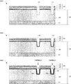
次いで、図2に示したステップS210、S220、図3に示したS230において、半導体基板SSにトレンチTRを形成するトレンチ形成工程が実施される。まず、ステップS210において、半導体基板SSの上に膜150を形成する工程が実施される。膜150は、例えば、酸化シリコン層151と、酸化シリコン層151の上に配置されたポリシリコン層152と、ポリシリコン層152の上に配置された窒化シリコン層153とを含みうる。ステップS210に次いで、ステップS220において、膜150をフォトリソグラフィー工程によってパターニングして開口OP1を形成する工程が実施される。ステップS220に次いで、ステップS230において、パターニングされた膜150をエッチングマスクとして開口OP1を通して半導体基板SS(第2半導体領域102)をエッチングする工程が実施される。この工程により、半導体基板SS(第2半導体領域102)にトレンチTRが形成される。
Next, in steps S210 and S220 shown in FIG. 2 and S230 shown in FIG. 3, a trench forming step of forming a trench TR in the semiconductor substrate SS is performed. First, in step S210, a step of forming the
次いで、図3に示したステップS240において、酸素を含有する雰囲気中で半導体基板SSを熱処理。トレンチTRを形成することにより、トレンチTRの内面から第2半導体領域102の深部まで酸素を供給することができる。この熱処理は、トレンチTRの内面の酸化を伴い、その結果、トレンチTRの内面に酸化シリコン膜170が形成されうる。ステップS240における熱処理は、例えば、800℃以上1150℃以下の温度で実施されうる。また、ステップS240における熱処理は、例えば、第2半導体領域102の酸素濃度が2×10¹⁶atoms/cm3以上4×1017atoms/cm3以下の範囲内になるように実施されうる。また、ステップS240における熱処理は、例えば、第2半導体領域102の酸素濃度が1×1016atoms/cm3以上1×1017atoms/cm3以下の範囲内になるように実施されうる。
Next, in step S240 shown in FIG. 3, the semiconductor substrate SS is heat-treated in an atmosphere containing oxygen. By forming the trench TR, oxygen can be supplied from the inner surface of the trench TR to the deep portion of the
ここで、800℃以上1150℃以下の温度におけるシリコンへの酸素の固溶限界濃度は、2×10¹⁶atoms/cm3以上4×1017atoms/cm3以下の範囲である。そこで、半導体基板SSを得るための第1半導体領域101の酸素濃度を当該固溶限界濃度の範囲内の濃度とし、かつ、酸素を含有する雰囲気中でステップS240における熱処理を実施することが好ましい。このような方法によれば、深さ方向においてほぼ一定の酸素濃度分布を有する半導体基板SSを得ることが容易である。
Here, the solid solubility limit concentration of oxygen in silicon at a temperature of 800 ° C. or more and 1150 ° C. or less is in a range of 2 × 10 16 atoms / cm 3 or more and 4 × 10 17 atoms / cm 3 or less. Therefore, it is preferable to set the oxygen concentration of the
第2半導体領域102の深さ方向の全体において、ステップS240の熱処理の実施により、第2半導体領域102の酸素濃度を2×10¹⁶atoms/cm3以上4×1017atoms/cm3以下の範囲内にすることができる。また、第2半導体領域102の深さ方向の全体において、第2半導体領域102の酸素濃度が1×1016atoms/cm3以上1×1017atoms/cm3以下の範囲内にすることができる。また、例えば、ステップS240の後の、第2半導体領域102における酸素濃度の最大値、最小値をそれぞれC21max、C21minとしたときに、C21max/C21minが10以下であることが好ましい。C21max/C21minは5以下であることがより好ましい。
By performing the heat treatment in step S240 in the entire depth direction of the
図7には、ステップS240において酸素を含有する雰囲気中で熱処理が実施された後における半導体基板SSの深さ方向における酸素濃度の分布が実線で例示されている。ここで、図7に示された結果は、ステップS240の熱処理工程の温度を1050℃とした結果である。 FIG. 7 illustrates by solid lines the distribution of oxygen concentration in the depth direction of the semiconductor substrate SS after the heat treatment is performed in the atmosphere containing oxygen in step S240. Here, the result shown in FIG. 7 is a result of setting the temperature of the heat treatment step of step S240 to 1050 ° C.
ステップS240における熱処理では、半導体基板SSを加熱した後に半導体基板SSを強制的に冷却することにより、急速に冷却することができる。この冷却において、半導体基板SSの温度は、例えば、0.1℃/秒以上の温度降下率、好ましくは1℃/秒以上の温度降下率、更に好ましくは10℃/秒以上の温度降下率で降下されうる。温度降下率は100℃/秒以下でありうる。このように急速に冷却することにより、不要な酸素の拡散を抑制できる。 In the heat treatment in step S240, the semiconductor substrate SS can be cooled rapidly by heating the semiconductor substrate SS and then forcibly cooling the semiconductor substrate SS. In this cooling, the temperature of the semiconductor substrate SS is, for example, 0.1 ° C./sec or more, preferably 1 ° C./sec or more, more preferably 10 ° C./sec or more. Can be dropped. The rate of temperature drop can be less than 100 ° C./sec. By rapidly cooling in this manner, unnecessary diffusion of oxygen can be suppressed.
次いで、図3に示したステップS250において、第2導電型の不純物領域109を形成するための注入工程が実施される。トレンチTRの内面に沿って不純物領域109が形成されることで、トレンチTRの内面近傍で発生する暗電流を低減できる。ステップS240の熱処理を不純物領域109の形成の後に行うこともできるが、不純物領域109の形成をステップS240の熱処理熱の後に行うことにより、不純物領域109の不要な拡散を抑制できる。次いで、図4に示したステップS260において、トレンチTRに絶縁体160(酸化シリコン)を充填する充填工程が実施される。この際に、膜150の上にも絶縁体160が堆積しうる。図4では、酸化シリコン膜170を絶縁体160と一体的に記載している。次いで、図4に示したステップS270において、膜150の上の絶縁体160をCMP等によって除去する除去工程が実施される。これによりトレンチTR内に素子分離部110が形成される。その後、膜150が除去される。ステップS240の酸素雰囲気中での熱処理をステップS260の絶縁体160の埋め込みの後に行うこともできる。しかし、酸素雰囲気中での熱処理を絶縁体160の埋め込みの前に行うことで、トレンチTRの内面から第2半導体領域102の深部まで酸素を供給できる。
Next, in step S250 shown in FIG. 3, an implantation process for forming
次いで、図4に示したステップS280においては、第2導電型の不純物領域103、第2導電型の不純物領域106、107が形成される。なお、第2導電型の不純物領域103、第2導電型の不純物領域106、107を形成するためのレジストパターンは、省略されている。そして、形成された第2導電型の不純物領域103、106、107を拡散あるいは活性化させるために、酸素を含有しない雰囲気中で熱処理工程を行う。その後、ステップ280において、半導体基板SSの上にゲート絶縁膜116、117およびゲート電極114、115が形成される。
Next, in step S280 shown in FIG. 4, the second conductivity
図8には、ステップS280の後における半導体基板SSの深さ方向における酸素濃度の分布が実線で例示されている。図8の状態では、上述した酸素を含有しない雰囲気中での熱処理工程や、さらにゲート絶縁膜116、117の形成のために酸素を含有する雰囲気中での熱処理工程などを経ている。酸素を含有しない雰囲気中で熱処理工程を実施した場合、半導体基板SSの表面に近い領域の酸素は、外方拡散によって脱離する。そのため、ステップS240の熱処理工程の直後(図7)と比べて、半導体基板SSの表面に近い領域における酸素の濃度が低くなる。図8に示された結果より、ステップS240の後に実施されうる熱処理(注入した不純物を活性化させるための熱処理、成膜処理)によっても酸素濃度の勾配が許容値内に抑えられることを理解することができる。第2半導体領域102の深さ方向の全体において、ステップS280の後でも、第2半導体領域102の酸素濃度を2×10¹⁶atoms/cm3以上4×1017atoms/cm3以下の範囲内に維持することができる。また、第2半導体領域102の深さ方向の全体において、第2半導体領域102の酸素濃度が1×1016atoms/cm3以上1×1017atoms/cm3以下の範囲内に維持することができる。また、例えば、ステップS280の後でも、第2半導体領域102における酸素濃度の最大値、最小値をそれぞれC22max、C22minとしたときに、C22max/C22minが10以下であることが好ましい。C22max/C22minは5以下であることがより好ましい。
FIG. 8 illustrates the distribution of the oxygen concentration in the depth direction of the semiconductor substrate SS after step S280 by a solid line. In the state of FIG. 8, the above-described heat treatment step in an atmosphere containing no oxygen and the heat treatment step in an atmosphere containing oxygen for forming the
次いで、ステップS290において、半導体基板SSの上にレジストパターンRP2が形成されレジストパターンRP2の開口OP2を通して半導体基板SS(第2半導体領域102)に第1導電型の不純物が注入され、これにより不純物領域104が形成される。その後、レジストパターンRP2が除去される。 Next, in step S290, a resist pattern RP2 is formed on the semiconductor substrate SS, and a first conductivity type impurity is implanted into the semiconductor substrate SS (second semiconductor region 102) through the opening OP2 of the resist pattern RP2. 104 is formed. After that, the resist pattern RP2 is removed.
次いで、ステップS300において、半導体基板SSの上にレジストパターンRP3が形成され、レジストパターンRP3の開口OP3を通して半導体基板SSに第2導電型の不純物が注入される。これにより第2導電型の不純物領域105が不純物領域104の上に形成される。このようにステップS200〜S300に渡って光電変換素子PDが形成される。
Next, in step S300, a resist pattern RP3 is formed on the semiconductor substrate SS, and a second conductivity type impurity is implanted into the semiconductor substrate SS through the opening OP3 of the resist pattern RP3. As a result, the
次いで、ステップS310において、半導体基板SSの表面およびゲート電極114、115を覆うように絶縁層118が形成される。その後、複数の絶縁層123、配線層120、122、コンタクトプラグ119およびビアプラグ121などが形成され、更に、カラーフィルタ層124およびマイクロレンズ125などが形成される。これにより、図1に例示されるよう撮像装置100が完成する。
Next, in step S310, an insulating
図9には、この実施形態に従って製造された撮像装置100の半導体基板SSにおける酸素濃度の分布が実線で例示されている。図9には、比較例も示されている。比較例では、半導体基板SSの表面から10μm程度の深さにおける酸素濃度が7×10¹⁷atoms/cm3であり、表面近傍の酸素濃度である7×1016atoms/cm3の約10倍であり、濃度勾配が極めて大きい。これに対して、この実施形態では、半導体基板SSの表面から10μm程度の深さでも酸素濃度が8×1016atoms/cm3であり、表面近傍の酸素濃度である5×1016atoms/cm3の1.6倍程度の濃度である。つまり、この実施形態では、酸素濃度の勾配が低い状態が達成されている。濃酸素度の勾配が低い状態であれば、製造プロセスのばらつきが発生しても、それに起因する残像の発生を抑えることができる。製造プロセスのばらつきとしては、例えば、第1半導体領域101を切り出すためのインゴットまたは第1半導体領域101における酸素濃度のばらつきを挙げることができる。その他の製造プロセスのばらつきとして、例えば、不純物を半導体基板SSに注入した後に該不純物を活性化させるための熱処理、あるいは、成膜処理における温度ばらつきを挙げることができる。
FIG. 9 illustrates the distribution of the oxygen concentration in the semiconductor substrate SS of the
撮像装置100において、半導体基板SSにおける残像に対する影響が大きい深さ部分における酸素濃度の最大値、最小値をそれぞれCmax、Cminとしたときに、Cmax/Cminが10以下であることが好ましい。例えば、撮像装置100において、半導体基板SSの表面からの距離が20μm以内の部分における半導体領域の酸素濃度の最大値、最小値をそれぞれCmax、Cminとしたときに、Cmax/Cminが10以下であることが好ましい。あるいは、撮像装置100において、半導体基板SSの表面からの距離が30μm以内の部分における半導体領域の酸素濃度の最大値、最小値をそれぞれCmax、Cminとしたときに、Cmax/Cminが10以下であることが好ましい。あるいは、撮像装置100において、半導体基板SSの表面からの距離が40μm以内の部分における半導体領域の酸素濃度の最大値、最小値をそれぞれCmax、Cminとしたときに、Cmax/Cminが10以下であることが好ましい。あるいは、撮像装置100において、半導体基板SSの表面からの距離が50μm以内の部分における半導体領域の酸素濃度の最大値、最小値をそれぞれCmax、Cminとしたときに、Cmax/Cminが10以下であることが好ましい。それぞれの深さの部分において、Cmax/Cminは5以下であることが好ましい。
In the
なお、半導体基板SSの表面からの深さが10μm以内の部分における酸素濃度の最大値、最小値をそれぞれCmax、Cminとしたときに、Cmax/Cminの値は、図9に示された実施形態では1.6、図9に示された比較例では約10である。つまり、図9に示された比較例のCmax/Cminの値は、図9に示された実施形態のCmax/Cminの値よりも、かなり大きく、残像の発生が大きいことが推定される。 In addition, when the maximum value and the minimum value of the oxygen concentration in a portion whose depth from the surface of the semiconductor substrate SS is within 10 μm are Cmax and Cmin, respectively, the value of Cmax / Cmin is equal to the embodiment shown in FIG. Is 1.6, and about 10 in the comparative example shown in FIG. That is, it is estimated that the value of Cmax / Cmin of the comparative example shown in FIG. 9 is considerably larger than the value of Cmax / Cmin of the embodiment shown in FIG.
以下、上記の各実施形態に係る撮像装置の応用例として、該撮像装置が組み込まれたカメラについて例示的に説明する。カメラの概念には、撮影を主目的とする装置のみならず、撮影機能を補助的に備える装置(例えば、パーソナルコンピュータ、携帯端末)も含まれる。カメラは、上記の実施形態として例示された本発明に係る撮像装置と、該撮像装置から出力される信号を処理する処理部とを含む。該処理部は、例えば、A/D変換器、および、該A/D変換器から出力されるデジタルデータを処理するプロセッサを含みうる。 Hereinafter, as an application example of the imaging device according to each of the above embodiments, a camera incorporating the imaging device will be illustratively described. The concept of the camera includes not only a device mainly for photographing but also a device (for example, a personal computer or a portable terminal) having a supplementary photographing function. The camera includes the imaging device according to the present invention exemplified as the above embodiment, and a processing unit that processes a signal output from the imaging device. The processing unit may include, for example, an A / D converter and a processor that processes digital data output from the A / D converter.
以上説明した実施形態は撮像装置として表面照射型のCMOSイメージセンサを例示したが、裏面照射型にも適用可能であるし、CCDイメージセンサにも適用可能である。裏面照射型の撮像装置においては、光電変換部を有する単結晶シリコンからなる半導体領域の厚さは1〜10μm程度である。半導体領域の表面から裏面まで、深さ方向の全域で半導体領域の酸素濃度の最大値が最小値の10倍以下であればよい。半導体領域の表面から裏面まで、深さ方向の全域で半導体領域の酸素濃度2×10¹⁶atoms/cm3以上4×1017atoms/cm3以下範囲内であればよい。半導体領域の表面から20μmまでの範囲のうち、半導体領域の裏面よりも表面から遠い部分には、酸素起因の残像を生じせしめるような半導体領域は存在せずに、マイクロレンズやカラーフィルタが存在しうる。
In the above-described embodiment, a front-side illuminated CMOS image sensor has been illustrated as an image pickup apparatus. In a back-illuminated imaging device, the thickness of a semiconductor region made of single crystal silicon having a photoelectric conversion unit is about 1 to 10 μm. It is sufficient that the maximum value of the oxygen concentration in the semiconductor region is 10 times or less the minimum value in the entire depth direction from the front surface to the back surface of the semiconductor region. It is sufficient that the oxygen concentration in the semiconductor region is in the range of 2 × 10 16 atoms /
以下、添付図面を参照しながら本発明の他の側面をその例示的な実施形態である第2実施形態を通して説明する。 Hereinafter, another aspect of the present invention will be described with reference to the accompanying drawings through a second embodiment which is an exemplary embodiment.
撮像装置は、例えば、シリコン等の半導体で構成された基板に配列され且つ各々が光電変換部を含む複数の画素を有しており、各画素で光電変換により発生した電荷に基づいて画像が形成される。 The imaging device has, for example, a plurality of pixels arranged on a substrate made of a semiconductor such as silicon and each including a photoelectric conversion unit, and forms an image based on charges generated by photoelectric conversion in each pixel. Is done.
撮像装置には、画像に生じうる残像および白キズを抑制ないし低減することが求められる。残像は、例えば、ある画像を読み出す際に、光電変換により発生した電荷が基板中の欠陥等にトラップされ、その後の他の画像を読み出す際に、該電荷がリリースされることに起因して生じうる。白キズは、撮像装置の製造の間、例えば、トランジスタの電極をニッケルやコバルトによりシリサイド化する工程において基板中に混入した金属不純物に起因して生じうる。 An imaging device is required to suppress or reduce afterimages and white spots that may occur in an image. Afterimages are generated, for example, when a certain image is read out, charges generated by photoelectric conversion are trapped by defects or the like in a substrate, and then, when another image is read out, the charges are released. sell. White flaws can occur during the manufacturing of the imaging device, for example, due to metal impurities mixed into the substrate in the step of silicidizing the electrode of the transistor with nickel or cobalt.
特開2007−251074号公報には、基板中の酸素濃度を低くすることによって画像中の残像を抑制することが開示されている。一方で、特開2003−92301号公報には、基板中の酸素濃度を高くすることによって画像中の白キズを抑制することが開示されている。即ち、特開2007−251074号公報及び特開2003−92301号公報によると、残像の抑制および白キズの抑制の双方を達成するには、互いに相反する構成が基板に要求される。したがって、これら双方を、単に基板中の酸素濃度を調整することによって達成することは難しいと言える。 Japanese Patent Application Laid-Open No. 2007-251074 discloses that an afterimage in an image is suppressed by lowering the oxygen concentration in a substrate. On the other hand, Japanese Patent Application Laid-Open No. 2003-92301 discloses that white defects in an image are suppressed by increasing the oxygen concentration in a substrate. In other words, according to JP-A-2007-251074 and JP-A-2003-92301, in order to achieve both suppression of afterimages and suppression of white spots, mutually contradictory configurations are required for a substrate. Therefore, it can be said that it is difficult to achieve both of them simply by adjusting the oxygen concentration in the substrate.
本実施形態は、画像中の残像および白キズの双方を抑制する新規な技術を提供することを目的とする。 An object of the present embodiment is to provide a novel technique for suppressing both afterimages and white defects in an image.
本実施形態の一つの側面は撮像装置にかかり、前記撮像装置は、シリコンで構成された基板上に複数の画素が配列された画素部と、前記基板上の前記画素部の周辺に配された周辺回路部であって各画素からの信号を処理する回路を含む周辺回路部と、を有する。
ここで、前記周辺回路部は、ニッケル及びコバルトの少なくとも一方を含むシリサイド領域を有するトランジスタを有する。
また、各画素は、前記基板に形成され、
光電変換により発生した電荷を蓄積する部分を含む第1導電型の第1領域と、
前記基板の前記第1領域より深い位置であって前記第1領域から離れた位置に配された前記第1導電型の第2領域と、
前記基板の表面からの深さ方向において、前記第1領域と前記第2領域との間に配された第2導電型の第3領域と、を有する。
また、前記第3領域は、
前記深さ方向において前記第2領域から離れた位置に配され、前記第2導電型の正味の不純物濃度が第1極大値を示す位置を含む第1部分と、
前記深さ方向において前記第1部分と前記第2領域との間に配され、前記第2導電型の正味の不純物濃度が前記第1極大値よりも低い第2極大値を示す位置を含む第2部分と、を含む。
前記第2部分の酸素濃度は1×10¹⁷[atoms/cm3]以下である。
One aspect of the present embodiment relates to an imaging device, and the imaging device is disposed around a pixel portion in which a plurality of pixels are arranged on a substrate made of silicon and around the pixel portion on the substrate. A peripheral circuit section including a circuit for processing a signal from each pixel.
Here, the peripheral circuit section has a transistor having a silicide region containing at least one of nickel and cobalt.
Also, each pixel is formed on the substrate,
A first region of a first conductivity type including a portion for accumulating charges generated by photoelectric conversion,
A second region of the first conductivity type, which is disposed at a position deeper than the first region of the substrate and away from the first region;
A third region of a second conductivity type disposed between the first region and the second region in a depth direction from a surface of the substrate.
Further, the third region is
A first portion disposed at a position apart from the second region in the depth direction, the first portion including a position at which a net impurity concentration of the second conductivity type exhibits a first maximum value;
A second portion disposed between the first portion and the second region in the depth direction, the second portion including a position where a net impurity concentration of the second conductivity type indicates a second maximum value lower than the first maximum value; And two parts.
The second portion has an oxygen concentration of 1 × 10 17 [atoms / cm 3 ] or less.
本実施形態によれば、画像中の残像および白キズの双方を抑制することができる。
(1−1.撮像装置の構造について)
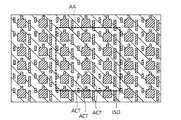
図10は、第2実施形態に係る撮像装置100の構造の例を説明するための模式図である。撮像装置100は、シリコンで構成された基板SUBにそれぞれ形成された領域R1〜R4等を備える。領域R1(第1領域)は、例えばN型(第1導電型)であり、本明細書において、以下「N型領域R1」と示す。領域R2(第2領域)は、例えばN型であり、以下「N型領域R2」と示す。領域R3(第3領域)は、例えばP型(第2導電型)であり、以下「P型領域R3」と示す。また、領域R4は、例えばN型であり、以下「N型領域R4」と示す。
According to the present embodiment, it is possible to suppress both afterimages and white spots in an image.
(1-1. Structure of imaging device)
FIG. 10 is a schematic diagram for explaining an example of the structure of the
上記領域R1〜R4のそれぞれは、例えば、エピタキシャル成長、不純物注入等の公知の半導体製造技術を用いて形成されればよい。具体的には、まず、N型領域R4に対応するシリコン基板を準備し、その上にN型の半導体部材を例えばエピタキシャル成長によって形成する。次に、該形成された半導体部材に不純物注入によって、N型領域R1を形成し、N型領域R1の形成前または後にN型領域R1より深い位置にP型領域R3を形成する。N型領域R2は、P型領域R3とN型領域R4との間の領域であり、したがって、N型領域R1より深い位置であってN型領域R1から離れた位置に配されている。 Each of the regions R1 to R4 may be formed using a known semiconductor manufacturing technique such as epitaxial growth and impurity implantation. Specifically, first, a silicon substrate corresponding to the N-type region R4 is prepared, and an N-type semiconductor member is formed thereon by, for example, epitaxial growth. Next, an N-type region R1 is formed by implanting impurities into the formed semiconductor member, and a P-type region R3 is formed at a position deeper than the N-type region R1 before or after the formation of the N-type region R1. The N-type region R2 is a region between the P-type region R3 and the N-type region R4, and is therefore arranged at a position deeper than the N-type region R1 and apart from the N-type region R1.
N型領域R1は、光電変換によって発生した電荷(この例では電子)が蓄積される部分である電荷蓄積部(不図示)であって、他の部分よりも高い不純物濃度(例えば1×10¹⁷[cm−3]以上)を有する電荷蓄積部を含む。N型領域R1は、基板SUBの表面近傍にP型の領域R0が形成されることによって、基板SUBの表面から離れた位置に(埋め込まれるように)形成されてもよい。 The N-type region R1 is a charge storage portion (not shown) in which charges (electrons in this example) generated by photoelectric conversion are stored, and has a higher impurity concentration (for example, 1 × 10 17 ) than other portions. [Cm −3 ] or more. The N-type region R1 may be formed at a position away from the surface of the substrate SUB (so as to be embedded) by forming the P-type region R0 near the surface of the substrate SUB.
P型領域R3は、N型領域R1とN型領域R2との間に、N型領域R1の底面および側面と接触するように形成された領域である。即ち、N型領域R1とP型領域R3との間にはPN接合が形成されており、フォトダイオードが形成されている。換言すると、P型領域R3は、N型領域R1と隣接するように、N型領域R1またはそれより浅い位置から、N型領域R1より深く且つN型領域R2より浅い位置までにわたって形成されている。 The P-type region R3 is a region formed between the N-type region R1 and the N-type region R2 so as to be in contact with the bottom surface and the side surface of the N-type region R1. That is, a PN junction is formed between the N-type region R1 and the P-type region R3, and a photodiode is formed. In other words, the P-type region R3 is formed so as to be adjacent to the N-type region R1 and extend from a position shallower than the N-type region R1 to a position deeper than the N-type region R1 and shallower than the N-type region R2. .
なお、上述の各領域において、P型を形成するための不純物(P型不純物)には、例えばボロン(B)等が用いられ、N型を形成するための不純物(N型不純物)には、例えばリン(P)、ヒ素(As)等が用いられればよい。また、図中には、N型領域R1におけるN型不純物濃度の極大値Q_R1、および、P型領域R3におけるP型不純物濃度の極大値Q1〜Q5が示されているが、これらについての詳細は後述とする。 In each of the above regions, for example, boron (B) is used as an impurity for forming a P-type (P-type impurity), and an impurity (N-type impurity) for forming an N-type is For example, phosphorus (P), arsenic (As), or the like may be used. In the figure, the maximum value Q_R1 of the N-type impurity concentration in the N-type region R1 and the maximum values Q1 to Q5 of the P-type impurity concentration in the P-type region R3 are shown. It will be described later.
撮像装置100は、フローティングディフュージョンFDと、ゲート電極GTXとをさらに備える。フローティングディフュージョンFDは、基板SUB表面およびその近傍かつN型領域R1から離れた位置に形成されたN型領域である。ゲート電極GTXは、N型領域R1とフローティングディフュージョンFDとを接続するMOSトランジスタ(転送トランジスタ)のゲート電極であり、基板SUB上に絶縁膜Fを介して形成される。光電変換により発生しN型領域R1に蓄積された電荷は、ゲート電極GTXに活性化電圧を供給することで形成されるチャネルを介して、フローティングディフュージョンFDに転送される。該転送された電荷またはそれに応じた信号は、不図示の読出回路によって画素信号として読み出される。
The
また、撮像装置100は、基板SUBの表面近傍に形成されたSTI(ShallowTrench Isolation)構造を有する素子分離部STIと、その周囲に形成されたチャネルストップ用のP型の不純物領域CSとをさらに備える。素子分離部STIは、基板SUBに形成された素子ないしユニットを互いに電気的に分離する。
The
ここでは説明を省略するが、基板SUBの上には、1以上の配線層に配された導電部材(配線パターン)及びそれらを接続するプラグ、光学素子(例えば、カラーフィルタ、マイクロレンズ等)を含む構造が配されうる。 Although not described here, conductive members (wiring patterns) arranged in one or more wiring layers, plugs for connecting them, and optical elements (eg, color filters, microlenses, etc.) are provided on the substrate SUB. Included structures can be arranged.
図11は、図10におけるカットラインA1−A2(基板SUBの表面からの深さ方向)での不純物(ボロンおよびヒ素)の実際の濃度分布を示している。なお、ここでは、本例の説明に必要な部分の不純物濃度のみを図示し、それ以外の部分(例えば領域R0等)の不純物濃度分布については不図示とする。 FIG. 11 shows the actual concentration distribution of impurities (boron and arsenic) at cut lines A1-A2 (in the depth direction from the surface of the substrate SUB) in FIG. Here, only the impurity concentration of a portion necessary for the description of the present example is shown, and the impurity concentration distribution of other portions (for example, the region R0) is not shown.
ここで、ある領域における“実際”の不純物濃度とは、その領域の導電型に関わらず、その領域に実際に存在する不純物濃度であり、グロス(gross)不純物濃度とも呼ばれる。一方、ある領域における“正味”の不純物濃度とは、その領域の導電型を決定する実効的な不純物濃度であり、ネット(net)不純物濃度とも呼ばれる。即ち、正味の不純物度濃度は、一方の導電型の実際の不純物濃度から、該導電型とは異なる他方の導電型の実際の不純物濃度を減算したものに対応する。例えば、ある領域における実際のボロン(P型不純物)濃度が4×10¹⁶[cm−3]且つ実際のヒ素(N型不純物)濃度が1×10¹⁶[cm−3]のとき、その領域の導電型はP型であり、その領域の正味のP型不純物濃度は3×10¹⁶[cm−3]である。 Here, the “actual” impurity concentration in a certain region is an impurity concentration actually existing in the region regardless of the conductivity type of the region, and is also referred to as a gross impurity concentration. On the other hand, the “net” impurity concentration in a certain region is an effective impurity concentration that determines the conductivity type of the region, and is also called a net impurity concentration. That is, the net impurity concentration corresponds to the actual impurity concentration of one conductivity type minus the actual impurity concentration of the other conductivity type different from the other conductivity type. For example, when the actual boron (P-type impurity) concentration in a certain region is 4 × 10 16 [cm −3 ] and the actual arsenic (N-type impurity) concentration is 1 × 10 16 [cm −3 ], The conductivity type is P-type, and the net P-type impurity concentration in the region is 3 × 10 16 [cm −3 ].
図11には実際の不純物濃度を記載しているが、N型領域R1におけるP型の不純物濃度は、N型領域R1におけるN型の不純物濃度よりも十分に低く、また、P型領域R2におけるN型の不純物濃度は、P型領域R2におけるP型の不純物濃度よりも十分に低い。そのため、図11に対応する正味の不純物濃度分布は、実質的に、図11の不純物分布と同様の分布となる。 FIG. 11 shows the actual impurity concentration. However, the P-type impurity concentration in the N-type region R1 is sufficiently lower than the N-type impurity concentration in the N-type region R1. The N-type impurity concentration is sufficiently lower than the P-type impurity concentration in P-type region R2. Therefore, the net impurity concentration distribution corresponding to FIG. 11 is substantially the same as the impurity distribution of FIG.
図11において、N型領域R1のN型不純物(ヒ素)濃度を一点鎖線で図示し、また、P型領域R3のP型不純物(ボロン)濃度を実線で図示している(なお、基板SUB中の酸素濃度を破線で図示しているが、これについての詳細は後述とする。)。N型領域R1においてN型不純物濃度が極大値C_R1を示す位置をピーク位置Q_R1とする。前述の光電変換によって発生した電荷は、主に、N型領域R1におけるピーク位置Q_R1及びその近傍(例えば1×10¹⁶[cm−3]以上の部分、特に、1×10¹⁷[cm−3]以上の部分)に蓄積されうる。ピーク位置Q_R1は、深さ(基板SUBの表面からの深さ)0.3[μm]程度で、その正味のN型不純物濃度は1.23×10¹⁷[cm−3]程度である。N型領域R1における電荷蓄積部以外の部分については、正味のN型不純物濃度は、1×10¹⁷[cm−3]未満でもよく、例えば1×10¹⁴〜1×10¹⁶[cm−3]程度でもよい。 In FIG. 11, the N-type impurity (arsenic) concentration in the N-type region R1 is shown by a dashed-dotted line, and the P-type impurity (boron) concentration in the P-type region R3 is shown by a solid line (in the substrate SUB). Is shown by a broken line, the details of which will be described later.) The position where the N-type impurity concentration shows the maximum value C_R1 in the N-type region R1 is defined as a peak position Q_R1. The charges generated by the above-mentioned photoelectric conversion mainly include the peak position Q_R1 in the N-type region R1 and the vicinity thereof (for example, a portion of 1 × 10 16 [cm −3 ] or more, particularly 1 × 10 17 [cm −3 ]). Above). The peak position Q_R1 has a depth (depth from the surface of the substrate SUB) of about 0.3 [μm] and a net N-type impurity concentration of about 1.23 × 10 17 [cm −3 ]. For the portion other than the charge accumulation portion in the N-type region R1, the net N-type impurity concentration may be lower than 1 × 10 17 [cm −3 ], for example, 1 × 10 14 to 1 × 10 16 [cm −3 ]. Degree.
P型領域R3は、例えば、基板SUBの表面からの深さ方向において、複数の部分P0〜P5を有する。本例において、部分P0は、領域R1を取り囲む部分である。部分P1〜P5は、P型不純物濃度が極大値C1〜C5をそれぞれ示す位置Q1〜Q5をそれぞれ含む。図中に、部分P1、P2、P3、P4、P5について、P型不純物濃度が極大値C1、C2、C3、C4、C5を示すピーク位置Q1、Q2、Q3、Q4、Q5をそれぞれ示す(P1〜P5及びQ1〜Q5は、図10にも図示されている。)。部分P0〜P5の境界は、正味のP型不純物濃度の分布における不純物濃度が極小値を示す位置とする。本構造は、例えば、複数回の不純物注入をそれぞれ互いに異なる注入エネルギーで行うことによって得られ、この方法によると、P型領域R3を、その不純物濃度分布が所望の濃度になるように調節しながら所望の深さまで形成することができる。 The P-type region R3 has, for example, a plurality of portions P0 to P5 in a depth direction from the surface of the substrate SUB. In this example, the portion P0 is a portion surrounding the region R1. The portions P1 to P5 include positions Q1 to Q5 at which the P-type impurity concentrations indicate the maximum values C1 to C5, respectively. In the figure, the peak positions Q1, Q2, Q3, Q4, and Q5 where the P-type impurity concentrations show the maximum values C1, C2, C3, C4, and C5 are shown for the portions P1, P2, P3, P4, and P5, respectively (P1). P5 and Q1 to Q5 are also illustrated in FIG. The boundary between the portions P0 to P5 is a position where the impurity concentration in the distribution of the net P-type impurity concentration shows the minimum value. This structure can be obtained, for example, by performing a plurality of times of impurity implantations with different implantation energies. According to this method, the P-type region R3 is adjusted while adjusting the impurity concentration distribution to a desired concentration. It can be formed to a desired depth.
P型領域R3において、部分P1〜P5のうち最も深い部分P5についての正味のP型不純物濃度を、部分P5以外の部分P1〜P4についての正味のP型不純物濃度より高くするとよい。例えば、部分P5についての正味のP型不純物濃度の極大値C5は、部分P1〜P4についての正味のP型不純物濃度の極大値C1〜C4の3倍以上高いとよく、5倍以上高いと更に良い。本構造によると、光電変換によってP型領域R3で発生した電荷の漏れ(具体的には、該電荷がP型領域R3よりも深い方向に漏れること)を防ぐことができ、該電荷を効率的にN型領域R1に導くことができる。 In the P-type region R3, the net P-type impurity concentration of the deepest portion P5 of the portions P1 to P5 may be higher than the net P-type impurity concentration of the portions P1 to P4 other than the portion P5. For example, the local maximum value C5 of the net P-type impurity concentration for the portion P5 is preferably at least three times higher than the local maximum values C1 to C4 of the net P-type impurity concentrations for the portions P1 to P4, and more than five times higher. good. According to this structure, it is possible to prevent the leakage of the charge generated in the P-type region R3 by the photoelectric conversion (specifically, the leakage of the charge in a direction deeper than the P-type region R3), and to efficiently reduce the charge. To the N-type region R1.
例えば、部分P1におけるピーク位置Q1は、深さ0.7[μm]程度で、その正味のP型不純物濃度の極大値C1は、2.0×10¹⁷[cm−3]程度である。部分P2におけるピーク位置Q2は深さ1.2[μm]程度で、その正味のP型不純物濃度の極大値C2は1.7×10¹⁷[cm−3]程度である。部分P3におけるピーク位置Q3は深さ1.6[μm]程度で、その正味のP型不純物濃度の極大値C3は1.0×10¹⁷[cm−3]程度である。部分P4におけるピーク位置Q4は深さ2.0[μm]程度で、その正味のP型不純物濃度の極大値C4は0.9×10¹⁷[cm−3]程度である。また、部分P5におけるピーク位置Q5は深さ3.2[μm]程度で、その正味のP型不純物濃度の極大値C5は4.0×10¹⁷[cm−3]程度である。部分P1〜P4における正味のP型不純物濃度の極大値C1〜C4は深い位置に配されるほど、小さくなっている(C1>C2>C3>C4)。なお、これらの深さは、入射光(例えば赤色光)の基板SUB表面からの侵入深さに基づいて定められればよい。 For example, the peak position Q1 in the portion P1 has a depth of about 0.7 [μm], and the maximum value C1 of the net P-type impurity concentration is about 2.0 × 10 17 [cm −3 ]. The peak position Q2 in the portion P2 has a depth of about 1.2 [μm], and the maximum value C2 of the net P-type impurity concentration is about 1.7 × 10 17 [cm −3 ]. The peak position Q3 in the portion P3 has a depth of about 1.6 [μm], and the maximum value C3 of the net P-type impurity concentration is about 1.0 × 10 17 [cm −3 ]. The peak position Q4 in the portion P4 has a depth of about 2.0 [μm], and the maximum value C4 of the net P-type impurity concentration is about 0.9 × 10 17 [cm −3 ]. The peak position Q5 in the portion P5 has a depth of about 3.2 [μm], and the maximum value C5 of the net P-type impurity concentration is about 4.0 × 10 17 [cm −3 ]. The maximum values C1 to C4 of the net P-type impurity concentration in the portions P1 to P4 become smaller as they are arranged at deeper positions (C1>C2>C3> C4). Note that these depths may be determined based on the penetration depth of incident light (for example, red light) from the surface of the substrate SUB.
(1−2.画像に生じうる白キズについて)
撮像装置100の製造過程において、基板SUB中には、例えばシリサイド処理によって、金属不純物(ニッケル、コバルト等)が混入する可能性があり、この金属不純物は、画像中に白キズをもたらす原因となりうる。このことに着目した本発明の発明者は、構成が互いに異なる複数の基板SUBを用いて実験し、鋭意検討した。そのなかで、発明者は、P型領域R3のP型不純物濃度分布が互いに異なる複数の基板SUBを用いた実験により、上記白キズの程度が、N型領域R1‐P型領域R3間の空乏層の幅(体積)に依存することを見出した。具体的には、発明者は、N型領域R1‐P型領域R3間の空乏層内の金属不純物の数が多くなると画像中の白キズが増える傾向にあることを見出した。このことは、上記空乏層内の金属不純物が、その空乏層電界によって又は該電界を介してN型領域R1の蓄積電荷に何らかの影響を与えていることに起因すると考えられる。
(1-2. White flaws that can occur in images)
In the manufacturing process of the
そこで、本構造では、N型領域R1‐P型領域R3間の空乏層幅を小さくすることにより、白キズを抑制した。具体的には、P型領域R3のN型領域R1側の部分P1及びP2の正味のP型不純物濃度の極大値C1及びC2を、P型領域R3のN型領域R2側の部分P3及びP4の正味のP型不純物濃度の極大値C3及びC4よりも高くした。これにより、上記空乏層がP型領域R3の深い位置まで到達しないようにすることができる。また、P型領域R3のN型領域R1側の部分における正味のP型不純物濃度を、N型領域R1の電荷蓄積部における正味のN型不純物濃度よりも高くするとよい。具体的には、図11に例示されるように、P型領域R3の部分P1におけるピーク位置Q1の正味のP型不純物濃度を、N型領域R1におけるピーク位置Q_R1の正味のN型不純物濃度よりも高くするとよい。本構造によると、例えば、撮像装置100が電荷蓄積モード(N型領域R1に電荷を蓄積するための動作モード)の間、N型領域R1‐P型領域R3間の空乏層は、部分P1よりも深い部分P2〜P5に到達しないようにすることができる。
Therefore, in the present structure, white flaws are suppressed by reducing the width of the depletion layer between the N-type region R1 and the P-type region R3. Specifically, the local maximum values C1 and C2 of the P-type impurity concentration of the portions P1 and P2 of the P-type region R3 on the N-type region R1 side are changed to the portions P3 and P4 of the P-type region R3 on the N-type region R2 side. Were higher than the maximum values C3 and C4 of the net P-type impurity concentrations of the samples. Thereby, the depletion layer can be prevented from reaching the deep position of the P-type region R3. Further, it is preferable that the net P-type impurity concentration in the portion of the P-type region R3 on the N-type region R1 side is higher than the net N-type impurity concentration in the charge storage portion of the N-type region R1. Specifically, as illustrated in FIG. 11, the net P-type impurity concentration at the peak position Q1 in the portion P1 of the P-type region R3 is calculated from the net N-type impurity concentration at the peak position Q_R1 in the N-type region R1. Should be higher. According to this structure, for example, while the
まとめると、P型領域R3は、N型領域R1‐P型領域R3間の空乏層幅が小さくなるように構成されればよい。本例では、P型領域R3を、その一部の正味のP型不純物濃度が、該一部より深い位置の他の一部の正味のP型不純物濃度よりも高くなるように構成することにより、該他の一部に空乏層が到達しないようにしている。また、P型領域R3の該一部の正味のP型不純物濃度を、N型領域R1のピーク位置Q_R1の正味のN型不純物濃度よりも高くするとよい。好適には、P型領域R3の部分P1〜P5のうちN型領域R1に最も近い部分P1の正味のP型不純物濃度を、N型領域R1のピーク位置Q_R1の正味のN型不純物濃度よりも高くすればよい。 In summary, the P-type region R3 may be configured so that the depletion layer width between the N-type region R1 and the P-type region R3 is reduced. In this example, the P-type region R3 is configured such that the net P-type impurity concentration of a part thereof is higher than the net P-type impurity concentration of another part at a position deeper than the part. , So that the depletion layer does not reach the other part. Further, the net P-type impurity concentration of the part of the P-type region R3 may be higher than the net N-type impurity concentration of the peak position Q_R1 of the N-type region R1. Preferably, the net P-type impurity concentration of the portion P1 closest to the N-type region R1 among the portions P1 to P5 of the P-type region R3 is higher than the net N-type impurity concentration of the peak position Q_R1 of the N-type region R1. You only need to raise it.
また、本例において、部分P1と部分P5との間の部分P2〜P4の正味のP型不純物濃度の極大値C2〜C4は、部分P1の正味のP型不純物濃度の極大値C1よりも低くすることが好ましい。更に、部分P2〜P4の正味のP型不純物濃度の極大値C2〜C4を、部分P5の正味のP型不純物濃度の極大値C5よりも低くすることが好ましい。また更に、部分P2〜P4のいずれかの正味のP型不純物濃度を、N型領域R1の正味のN型不純物濃度よりも低くすることが好ましい。本例では、部分P3及びP4の正味のP型不純物濃度の極大値C3及びC4は、N型領域R1のピーク位置Q_R1の正味のN型不純物濃度の極大値C_R1よりも小さい。 Further, in this example, the maximum values C2 to C4 of the net P-type impurity concentration of the portions P2 to P4 between the portion P1 and the portion P5 are lower than the maximum value C1 of the net P-type impurity concentration of the portion P1. Is preferred. Furthermore, it is preferable that the maximum values C2 to C4 of the net P-type impurity concentrations of the portions P2 to P4 are lower than the maximum values C5 of the net P-type impurity concentrations of the portion P5. Further, it is preferable that the net P-type impurity concentration of any of the portions P2 to P4 is lower than the net N-type impurity concentration of the N-type region R1. In this example, the local maximum values C3 and C4 of the net P-type impurity concentration of the portions P3 and P4 are smaller than the local maximum value C_R1 of the net N-type impurity concentration at the peak position Q_R1 of the N-type region R1.
(1−3.画像に生じうる残像について)
基板SUB中の酸素濃度が高くなると、基板SUB中で酸素の複合体(サーマルドナー)が形成されやすくなる。サーマルドナーは、そのエネルギー準位により、光電変換によって生じた電荷をトラップする場合があり、このことは画像中に残像をもたらす原因となりうる。例えば、第1の画像を読み出す際に光電変換によって生じた電荷は、サーマルドナーのエネルギー準位によってトラップされうる。その後、第1の画像とは異なる第2の画像を読み出す際に、該トラップされた電荷がリリースされた場合、第2の画像には、この電荷に起因する残像が生じうる。
(1-3. Afterimages that can occur in images)
When the oxygen concentration in the substrate SUB increases, a complex of oxygen (thermal donor) is easily formed in the substrate SUB. The thermal donor may trap charges generated by photoelectric conversion depending on its energy level, and this may cause an afterimage in an image. For example, charge generated by photoelectric conversion when reading the first image can be trapped by the energy level of the thermal donor. Thereafter, when reading out a second image different from the first image, if the trapped charge is released, an afterimage due to the charge may occur in the second image.
特開2007−251074号公報によると、基板中の酸素濃度を低くすることによって画像中の残像が抑制される。その一方で、特開2003−92301号公報によると、基板中の酸素濃度を高くすることによって画像中の白キズが抑制される。 According to Japanese Patent Application Laid-Open No. 2007-251074, an afterimage in an image is suppressed by lowering the oxygen concentration in the substrate. On the other hand, according to JP-A-2003-92301, white flaws in an image are suppressed by increasing the oxygen concentration in the substrate.
ここで、図11を参照しながら述べたとおり、N型領域R1‐P型領域R3間の空乏層幅が小さくなるようにP型領域R3を構成することにより、白キズを抑制することができる。本構造において、残像を十分に抑制するために基板SUB中の酸素濃度をどのような範囲にすればよいか、発明者は、酸素濃度が互いに異なる複数の基板SUB(0.7×10¹⁷〜14×1017[atoms/cm3]程度)を用いて実験し、鋭意検討した。 Here, as described with reference to FIG. 11, white flaws can be suppressed by configuring the P-type region R3 so that the depletion layer width between the N-type region R1 and the P-type region R3 is reduced. . In the present structure, the inventor has determined what range of oxygen concentration in the substrate SUB should be set in order to sufficiently suppress the afterimage, and the inventor has determined that a plurality of substrates SUB (0.7 × 10 17 to The experiment was carried out using about 14 × 10 17 [atoms / cm 3 ], and intensive studies were conducted.
再び図11を参照すると、図11は、図10におけるカットラインA1−A2での基板SUB中の酸素濃度分布を更に示している。図11に示されるように、本構造では、基板SUB中の酸素濃度を1×10¹⁷[atoms/cm3]以下にし、上記残像を抑制した。 Referring again to FIG. 11, FIG. 11 further shows the oxygen concentration distribution in the substrate SUB at the cut line A1-A2 in FIG. As shown in FIG. 11, in the present structure, the oxygen concentration in the substrate SUB was set to 1 × 10 17 [atoms / cm 3 ] or less to suppress the afterimage.
ここで、光電変換により発生した電荷は、N型領域R1‐P型領域R3間の空乏層に到達すると、電界の大きい空乏層電界によってN型領域R1に向かってドリフトする。P型領域R3のうち、特に空乏化していない部分では、その電界が空乏層電界より小さいため、電荷がサーマルドナーのエネルギー準位にトラップされやすい(前述のとおり、このことは、画像中に残像が生じる原因となる。)。よって、この空乏化していない部分においてサーマルドナーが形成されないようにするとよく、少なくとも該空乏化していない部分における酸素濃度を1×10¹⁷[atoms/cm3]以下にするとよい。即ち、P型領域R3のうち正味のP型不純物濃度がN型領域R1のピーク位置Q_R1の正味のN型不純物濃度より高い位置又はそれを含む部分(本例では部分P1)から、それより深い部分までの酸素濃度を1×1017[atoms/cm3]以下にするとよい。好適には、P型領域R3全体を含む領域(N型領域R1又はそれより浅い位置からP型領域R3又はそれより深い位置までの領域)で、基板SUB中の酸素濃度を1×1017[atoms/cm3]以下にするとよい。P型領域R3より深い位置のN型領域R2では、酸素濃度は、P型領域R3での酸素濃度よりも高くてもよく、例えば1×1017[atoms/cm3]以上になってもよい。 Here, when the charge generated by the photoelectric conversion reaches the depletion layer between the N-type region R1 and the P-type region R3, it drifts toward the N-type region R1 due to the large electric field of the depletion layer. In the portion of the P-type region R3 that is not particularly depleted, the electric field is smaller than the electric field of the depletion layer, so that electric charges are easily trapped in the energy level of the thermal donor. Will cause this.) Therefore, it is preferable not to form a thermal donor in the non-depleted portion, and it is preferable that at least the oxygen concentration in the non-depleted portion be 1 × 10 17 [atoms / cm 3 ] or less. That is, in the P-type region R3, the position where the net P-type impurity concentration is higher than the net N-type impurity concentration at the peak position Q_R1 of the N-type region R1 or a portion including the same (the portion P1 in this example) is deeper than that. The oxygen concentration up to the portion is preferably set to 1 × 10 17 [atoms / cm 3 ] or less. Preferably, in a region including the entire P-type region R3 (a region from a position shallower than the N-type region R1 to a position deeper than the P-type region R3), the oxygen concentration in the substrate SUB is set to 1 × 10 17 [ atoms / cm 3 ] or less. In the N-type region R2 at a position deeper than the P-type region R3, the oxygen concentration may be higher than the oxygen concentration in the P-type region R3, and may be, for example, 1 × 10 17 [atoms / cm 3 ] or more. .
例えば、基板SUBの表面から、該表面から15[μm]の深さまでの領域(この領域は、P型領域R3を含むのに十分な深さを有する。)で、基板SUB中の酸素濃度を1×10¹⁷[atoms/cm3]以下にするとよい。他の例では、基板SUBの表面から、該表面から10[μm]の深さまでの領域で、基板SUB中の酸素濃度を1×1017[atoms/cm3]以下にしてもよい。そして、該表面から10[μm]の深さから、該表面から20[μm]の深さまでの領域で、基板SUB中の酸素濃度を2×1017[atoms/cm3]以下にしてもよい。さらに他の例では、前記基板の表面から10[μm]の深さから、該表面から20[μm]の深さまでの領域の一部では、基板SUB中の酸素濃度は1×1017[atoms/cm3]より大きくてもよい。 For example, in a region from the surface of the substrate SUB to a depth of 15 [μm] from the surface (this region has a depth sufficient to include the P-type region R3), the oxygen concentration in the substrate SUB is reduced. The density is preferably 1 × 10 17 [atoms / cm 3 ] or less. In another example, the oxygen concentration in the substrate SUB may be 1 × 10 17 [atoms / cm 3 ] or less in a region from the surface of the substrate SUB to a depth of 10 μm from the surface. Then, in a region from a depth of 10 [μm] from the surface to a depth of 20 [μm] from the surface, the oxygen concentration in the substrate SUB may be set to 2 × 10 17 [atoms / cm 3 ] or less. . In still another example, the oxygen concentration in the substrate SUB is 1 × 10 17 [atoms] in a part of a region from a depth of 10 [μm] from the surface of the substrate to a depth of 20 [μm] from the surface. / Cm 3 ].
また、第3領域R3の部分P1〜P5における酸素濃度は、図11に示されるように、1×10¹⁶[atoms/cm3]以上であってもよいことに留意されたい。1×1016[atoms/cm3]以上の酸素が存在することは、基板強度の向上、不純物金属のゲッタリングなどに有効である。本例では、ピーク位置C4とC5との間の領域における酸素濃度を、該領域における正味のP型不純物濃度よりも高くした。 Also, it should be noted that the oxygen concentration in the portions P1 to P5 of the third region R3 may be equal to or higher than 1 × 10 16 [atoms / cm 3 ], as shown in FIG. The presence of oxygen of 1 × 10 16 [atoms / cm 3 ] or more is effective in improving substrate strength, gettering of impurity metal, and the like. In this example, the oxygen concentration in the region between the peak positions C4 and C5 was higher than the net P-type impurity concentration in the region.
図12(a)は、画像中の残像についての基板SUB中の酸素濃度依存性の実測結果を示すプロット図である。図中の横軸は、基板SUB中の酸素濃度[atoms/cm3]を示し、縦軸は、画像中の残像の程度(残像量)[LSB]を示す。図12(a)によると、基板SUB中の酸素濃度を低くすると残像量が小さくなる。また、基板SUB中の酸素濃度が1×1017[atoms/cm3]以下の範囲では残像量が8[LSB]以下となり、画像中の残像を十分かつ効果的に低減することができる。 FIG. 12A is a plot diagram showing actual measurement results of the oxygen concentration dependency in the substrate SUB with respect to the afterimage in the image. The horizontal axis in the figure indicates the oxygen concentration [atoms / cm 3 ] in the substrate SUB, and the vertical axis indicates the degree of afterimage (afterimage amount) [LSB] in the image. According to FIG. 12A, the residual image amount decreases as the oxygen concentration in the substrate SUB decreases. When the oxygen concentration in the substrate SUB is 1 × 10 17 [atoms / cm 3 ] or less, the afterimage amount is 8 [LSB] or less, and the afterimage in the image can be sufficiently and effectively reduced.
図12(b)は、基板SUB中の酸素濃度が高い場合および低い場合、並びに、P型領域R3の正味のP型不純物濃度が高いおよび低い場合の個々について、残像量および白キズのそれぞれが許容範囲内か否かの判定結果をまとめたものである。図12(b)中の基板SUB中の酸素濃度の「高」は、該酸素濃度が1×10¹⁷[atoms/cm3]より高いことを示し、「低」は、該酸素濃度が1×1017[atoms/cm3]以下であることを示す。P型領域R3の正味のP型不純物濃度の「低」は、P型領域R3の少なくとも一部のP型不純物濃度がN型領域R1の正味のN型不純物濃度より低いことを示し、それ以外のケースを「高」と示す。 FIG. 12B shows that the residual image amount and the white flaw are respectively different when the oxygen concentration in the substrate SUB is high and low, and when the net P-type impurity concentration in the P-type region R3 is high and low. It is a summary of the determination result of whether or not the value is within the allowable range. “High” in the oxygen concentration in the substrate SUB in FIG. 12B indicates that the oxygen concentration is higher than 1 × 10 17 [atoms / cm 3 ], and “Low” indicates that the oxygen concentration is 1 × 10 17 [atoms / cm 3 ]. 10 17 [atoms / cm 3 ] or less. “Low” in the net P-type impurity concentration of the P-type region R3 indicates that the P-type impurity concentration of at least a part of the P-type region R3 is lower than the net N-type impurity concentration of the N-type region R1. Is indicated as “high”.
上述のそれぞれの場合について、残像/白キズについて、許容範囲内の結果には「○」で示し、そうでないものについては「×」で示す。例えば、図中において、残像が許容範囲内であり且つ白キズが許容範囲内でないものについては「○/×」と示す。図12(b)によると、基板SUB中の酸素濃度が「低」かつN型領域R2の正味のP型不純物濃度が「高」の場合に、残像および白キズの双方が許容範囲内になることが分かる。 In each of the above cases, the result within the allowable range for the afterimage / white defect is indicated by “○”, and the result other than that is indicated by “×”. For example, in the drawing, the case where the afterimage is within the allowable range and the white flaw is not within the allowable range is indicated by “○ / ×”. According to FIG. 12B, when the oxygen concentration in the substrate SUB is “low” and the net P-type impurity concentration in the N-type region R2 is “high”, both the afterimage and the white defect are within the allowable range. You can see that.
(1−4.まとめ)
本構造によると、P型領域R3を、その一部の正味のP型不純物濃度が、該一部より深い位置の他の一部の正味のP型不純物濃度よりも高くなるように構成することにより、該他の一部に空乏層が到達しないようにしている。これにより、N型領域R1‐P型領域R3間の空乏層幅を小さくし、画像中の白キズを抑制することができる。そして、基板SUB中の酸素濃度を1×10¹⁷[atoms/cm3]以下にすることにより、P型領域R3の深い部分でサーマルドナーが形成されないようにした。これにより、画像中の残像を抑制することができる。
(1-4. Summary)
According to this structure, the P-type region R3 is configured such that the net P-type impurity concentration of a part thereof is higher than the net P-type impurity concentration of another part at a position deeper than the part. This prevents the depletion layer from reaching the other part. Thereby, the width of the depletion layer between the N-type region R1 and the P-type region R3 can be reduced, and white flaws in an image can be suppressed. By setting the oxygen concentration in the substrate SUB to 1 × 10 17 [atoms / cm 3 ] or less, a thermal donor was prevented from being formed in a deep portion of the P-type region R3. Thereby, the afterimage in the image can be suppressed.
以上、本実施形態によると、画像中の残像および白キズの双方を抑制するのに有利である。 As described above, according to the present embodiment, it is advantageous to suppress both afterimages and white defects in an image.
特に、撮像装置100がデジタル回路を含む場合、撮像装置100の製造方法は、例えば、該デジタル回路内のトランジスタの各電極等をシリサイド化する工程を含みうるため、基板SUB中に金属不純物が混入してしまう可能性がある。例えば、撮像装置100は、複数の画素が配列された画素部と、その周辺に配された周辺回路部であって各画素からの信号を処理する周辺回路部とを備え、該周辺回路部のトランジスタには、ソース及びドレインにシリサイド領域を有するものが用いられうる。周辺回路部は、例えばアナログデジタル変換回路を含み、該シリサイド領域を有するトランジスタは、このアナログデジタル変換回路の一部にも用いられうる。シリサイド領域の金属には、典型的には、ニッケル、コバルト等が用いられ、その一部は、トランジスタをシリサイド化する工程(シリサイド領域を形成する工程)およびその後の熱処理工程により、不純物として画素部まで拡散しうる。前述のとおり、このことは画像における白キズの原因となりうる。よって、本実施形態によると、特にシリサイド化された領域を含む撮像装置100において、画像中の残像および白キズの双方を抑制するのに有利である。
In particular, when the
図13(a)〜(e)は、撮像装置100の製造方法における各工程の様子を説明するための模式図である。
FIGS. 13A to 13E are schematic diagrams for explaining the state of each step in the method of manufacturing the
図13(a)の工程では、酸素濃度が2×10¹⁷[atoms/cm3]以下の基板SUBであって、画素部が形成されるべき領域RA(画素領域)と、周辺回路部が形成されるべき領域RB(周辺領域)とを有する基板SUBを準備する。周辺領域RBは、例えば、NMOSトランジスタが形成されるべき領域RB1と、PMOSトランジスタが形成されるべき領域RB2とを含む。 In the step of FIG. 13A, the substrate SUB having an oxygen concentration of 2 × 10 17 [atoms / cm 3 ] or less, and a region RA (pixel region) where a pixel portion is to be formed and a peripheral circuit portion are formed A substrate SUB having an area RB (peripheral area) to be processed is prepared. The peripheral region RB includes, for example, a region RB1 where an NMOS transistor is to be formed and a region RB2 where a PMOS transistor is to be formed.
例えば、酸素濃度が1×10¹⁶[atoms/cm3]以上かつ3×1017[atoms/cm3]以下であるシリコンウエハの上に、エピタキシャル成長によって酸素濃度が1×1016[atoms/cm3]以下である単結晶シリコン層を形成する。シリコンウエハは、酸素濃度が3×1017[atoms/cm3]を超えないものが用いられることが望ましい。高酸素濃度(例えば1×1018[atoms/cm3]以上)のシリコンウエハを用いると、その上に低酸素濃度の単結晶シリコン層を形成したとしても、その後の他の工程(熱処理工程等)で、ウエハから単結晶シリコン層に酸素が移動(拡散)するからである。よって、シリコンウエハは、酸素濃度が少なくとも5×1017[atoms/cm3]以下のものが用いられるとよい。 For example, on a silicon wafer oxygen concentration is 1 × 10 16 [atoms / cm 3] or more and 3 × 10 17 [atoms / cm 3] or less, the oxygen concentration by epitaxial growth 1 × 10 16 [atoms / cm 3 The following single crystal silicon layer is formed. It is desirable to use a silicon wafer whose oxygen concentration does not exceed 3 × 10 17 [atoms / cm 3 ]. When a silicon wafer having a high oxygen concentration (for example, 1 × 10 18 [atoms / cm 3 ] or more) is used, even if a single crystal silicon layer having a low oxygen concentration is formed thereon, another process (such as a heat treatment process) is performed. This is because oxygen moves (diffuses) from the wafer to the single crystal silicon layer. Therefore, a silicon wafer having an oxygen concentration of at least 5 × 10 17 [atoms / cm 3 ] or less is preferably used.
なお、エピタキシャル成長によって形成される単結晶シリコン層は、その厚さが5〜25[μm]の範囲内になるように形成されるとよい。これにより、酸素濃度が比較的高いシリコンウエハを用いた場合でも、シリコンウエハ中の酸素が単結晶シリコン層の表面近傍まで拡散し得、単結晶シリコン層の酸素濃度が高くなることを防ぐことができる。 Note that the single crystal silicon layer formed by epitaxial growth is preferably formed to have a thickness in the range of 5 to 25 [μm]. Thus, even when a silicon wafer having a relatively high oxygen concentration is used, oxygen in the silicon wafer can diffuse to the vicinity of the surface of the single crystal silicon layer, thereby preventing the oxygen concentration of the single crystal silicon layer from increasing. it can.
準備した基板SUBにおいて、領域RA、RB1及びRB2の間には、例えばSTI構造の素子分離部STIを形成することができる。素子分離部STIは、例えば、酸化シリコン等の絶縁部材で構成されうる。素子分離部STIの深さは0.1〜0.5[μm]程度である。 In the prepared substrate SUB, for example, an element isolation portion STI having an STI structure can be formed between the regions RA, RB1, and RB2. The element isolation section STI can be formed of, for example, an insulating member such as silicon oxide. The depth of the element isolation part STI is about 0.1 to 0.5 [μm].
その後、画素領域RAにP型不純物を注入することによりP型領域R3を形成する。P型領域R3は、前述の部分P0〜P5を含む(ここでは部分P0〜P5を不図示とする。)。部分P0〜P5は、例えば、複数回の不純物注入を互いに異なる注入エネルギーで行うことにより形成されうる。 Thereafter, a P-type region R3 is formed by injecting a P-type impurity into the pixel region RA. The P-type region R3 includes the above-described portions P0 to P5 (the portions P0 to P5 are not illustrated here). The portions P0 to P5 can be formed, for example, by performing impurity implantation a plurality of times with mutually different implantation energies.
基板SUB表面の近傍には、後に形成されるトランジスタの閾値電圧を調節するため、例えば、P型あるいはN型の部分PA、PB及びPCが形成されてもよい。また、基板SUBのうち素子分離部STIと接触する部分には、素子分離部STIと基板SUBとの境界の結晶欠陥に起因して画素信号に混入しうる暗電流成分を低減するため、素子分離部STIを取り囲むようにP型の領域CSが形成されていてもよい。 For example, P-type or N-type portions PA, PB, and PC may be formed near the surface of the substrate SUB in order to adjust the threshold voltage of a transistor to be formed later. In addition, a portion of the substrate SUB that is in contact with the element isolation portion STI is provided with an element isolation portion to reduce a dark current component that can be mixed into a pixel signal due to a crystal defect at a boundary between the element isolation portion STI and the substrate SUB. A P-type region CS may be formed so as to surround portion STI.
図13(b)の工程では、例えば、基板SUB上に形成された所定のレジストパターン(不図示)を用いて、不純物注入により領域RB1にP型ウエルPWLを形成する。その後、同様の手順で、領域RB2にN型ウエルNWLを形成する。これらのウエルは、いずれが先に形成されてもよい。 In the step of FIG. 13B, for example, a P-type well PWL is formed in the region RB1 by implanting impurities using a predetermined resist pattern (not shown) formed on the substrate SUB. Thereafter, an N-type well NWL is formed in the region RB2 by the same procedure. Any of these wells may be formed first.
図13(c)の工程では、基板SUB表面に絶縁膜F(トランジスタのゲート絶縁膜)を形成する。絶縁膜Fは、例えば酸化シリコンで構成され、その膜厚は3〜20[nm]程度とすればよい。その後、絶縁膜Fの上に、転送トランジスタのゲート電極GTX、他のMOSトランジスタのゲート電極Gが形成される。また、基板SUBの表面およびその近傍には、N型不純物を注入することにより、N型領域R1が形成される。N型領域R1は、前述のピーク位置Q_R1が、素子分離部STIの深さの半分より深くなるように形成されるとよく、好適には、素子分離部STIの底面よりも深くなるように形成されてもよい。 In the step of FIG. 13C, an insulating film F (gate insulating film of a transistor) is formed on the surface of the substrate SUB. The insulating film F is made of, for example, silicon oxide, and its thickness may be about 3 to 20 [nm]. Thereafter, a gate electrode GTX of the transfer transistor and a gate electrode G of another MOS transistor are formed on the insulating film F. An N-type region R1 is formed on the surface of the substrate SUB and in the vicinity thereof by implanting N-type impurities. The N-type region R1 is preferably formed so that the above-mentioned peak position Q_R1 is deeper than half of the depth of the element isolation portion STI, and is preferably formed deeper than the bottom surface of the element isolation portion STI. May be done.
さらにその後、ゲート電極GTXをマスクとして用いてフローティングディフュージョンFDが形成されうる。また、領域RB1及びRB2のそれぞれには、対応するMOSトランジスタのソース/ドレイン領域RDSが形成されうる。 After that, the floating diffusion FD can be formed using the gate electrode GTX as a mask. In each of the regions RB1 and RB2, a source / drain region RDS of a corresponding MOS transistor can be formed.
なお、上記画素を構成する各要素の形成順序は必要に応じて変更されてもよい。例えば、ゲート電極GTX及びN型領域R1について、それらのいずれが先に形成されてもよい。 Note that the order of forming the elements constituting the pixel may be changed as needed. For example, any of the gate electrode GTX and the N-type region R1 may be formed first.
図13(d)の工程では、N型領域R1を埋め込み型にするための領域R0を形成する。領域R0は、転送トランジスタの電荷転送効率が維持されるように、ゲート電極GTXの端から離れた位置に形成されうる。領域R0は、例えば、ゲート電極GTXおよびレジストパターンPRをマスクとして用いて、基板SUB(具体的にはN型領域R1の一部)にP型不純物を注入することによって為されればよい。該不純物の注入角度(基板SUB上面の法線と不純物の注入方向とが成す角)は、例えば7〜45度の範囲内で設定されるとよい。これにより、領域R0は、ゲート電極GTXの端から離れた位置に形成される。例えば、ゲート電極GTXの高さを250[nm]としたとき、上記注入は、12[keV]の注入エネルギーかつ10〜20度の範囲内の注入角度で為されればよい。 In the step of FIG. 13D, a region R0 for forming the N-type region R1 into a buried type is formed. The region R0 may be formed at a position away from the end of the gate electrode GTX so that the charge transfer efficiency of the transfer transistor is maintained. The region R0 may be formed, for example, by implanting a P-type impurity into the substrate SUB (specifically, a part of the N-type region R1) using the gate electrode GTX and the resist pattern PR as a mask. The impurity implantation angle (the angle between the normal line of the upper surface of the substrate SUB and the impurity implantation direction) may be set, for example, within a range of 7 to 45 degrees. As a result, the region R0 is formed at a position away from the end of the gate electrode GTX. For example, when the height of the gate electrode GTX is 250 [nm], the above-described implantation may be performed at an implantation energy of 12 [keV] and an implantation angle within a range of 10 to 20 degrees.
図13(e)の工程では、領域RA、RB1及びRB2を覆う絶縁膜を形成し、該絶縁膜の一部をエッチングして、ゲート電極Gの側面にサイドウォールスペーサSWSを形成する。このとき、該絶縁膜の他の一部は、保護膜PDPとして領域RAに残されうる。そして、N型不純物を注入することによって領域RB1のNMOSトランジスタをLDD構造にし、同様に、P型不純物を注入することによって領域RB2のPMOSトランジスタをLDD構造にする。その後、これらのMOSトランジスタに対してサリサイドプロセスを用いてシリサイド処理を行う。このとき、領域RAの保護膜PDPをシリサイドプロテクションとして用いることもできる。図中の部分Psiliは、各MOSトランジスタの電極のうちシリサイド化されたシリサイド領域を示している。 In the step of FIG. 13E, an insulating film covering the regions RA, RB1, and RB2 is formed, and a part of the insulating film is etched to form a sidewall spacer SWS on the side surface of the gate electrode G. At this time, another part of the insulating film may be left in the region RA as the protective film PDP. Then, the NMOS transistor in the region RB1 has an LDD structure by implanting an N-type impurity, and similarly, the PMOS transistor in the region RB2 has an LDD structure by implanting a P-type impurity. Thereafter, a silicide process is performed on these MOS transistors using a salicide process. At this time, the protective film PDP in the region RA can be used as silicide protection. A portion Psili in the figure indicates a silicide region which is silicided among the electrodes of each MOS transistor.
その後、図13(e)の工程で得られた構造の上に、公知の半導体製造技術を用いて、配線パターン、光学素子等を含む構造が形成されればよく、このようにして撮像装置100を製造することができる。 Thereafter, a structure including a wiring pattern, an optical element, and the like may be formed on the structure obtained in the step of FIG. 13E by using a known semiconductor manufacturing technique. Can be manufactured.
撮像装置100は、図13(a)を参照しながら述べたように、STI構造の素子分離部P1及びP2を備えうる。素子分離部P1及びP2は、例えばエッチング等によって基板SUBの表面から所定の深さまでにわたってトレンチを形成し、該トレンチを絶縁部材で埋めることによって形成されうる。この工程によると、基板SUB中に金属不純物が混入する可能性がある他、その間の熱処理に伴って基板SUBに加わる応力、形成された素子分離部P1及びP2によって基板SUBに加わる応力等により、画像中に白キズが生じる可能性がある。そのため、STI構造の素子分離部を含む撮像装置100に本発明を適用することによっても、画像中の残像および白キズの双方を抑制するのに有利である。
As described with reference to FIG. 13A, the
図14(a)〜(d)は、撮像装置100の製造方法におけるSTI構造の素子分離部(素子分離部Pとする。)の形成工程を説明するための図である。図14(a)の工程では、例えばシリコンで構成された基板SUB上にシリコン酸化膜F1、ポリシリコン膜F2、シリコン窒化膜F3がこの順に形成された構造を準備する。
FIGS. 14A to 14D are diagrams illustrating a process of forming an element isolation portion having an STI structure (referred to as an element isolation portion P) in the method of manufacturing the
図14(b)の工程では、例えば所定のレジストパターン(不図示)用いたエッチング等により、トレンチTを形成する。トレンチTは、シリコン窒化膜F3の上面から、基板SUBの表面から所定の深さまでにわたって形成されればよい。 In the step of FIG. 14B, the trench T is formed by, for example, etching using a predetermined resist pattern (not shown). The trench T may be formed from the upper surface of the silicon nitride film F3 to a predetermined depth from the surface of the substrate SUB.
図14(c)の工程では、例えば酸化処理を行い、トレンチTにより露出した基板SUBの露出面に酸化膜F4(酸化シリコン膜)を形成する。該酸化処理は、例えば、温度1100℃程度のドライ酸化で為されればよい。酸化膜F4の膜厚は20〜50[nm]程度とすればよい。 In the step of FIG. 14C, for example, an oxidation process is performed to form an oxide film F4 (silicon oxide film) on the exposed surface of the substrate SUB exposed by the trench T. The oxidation treatment may be performed, for example, by dry oxidation at a temperature of about 1100 ° C. The thickness of the oxide film F4 may be about 20 to 50 [nm].
なお、この工程において、基板SUBの上記露出面が酸化されると共に、トレンチTにより露出したポリシリコン膜F2の露出面(側面)も酸化される。これにより、ポリシリコン膜F2の露出面にも酸化シリコン膜が形成され、該酸化シリコン膜はトレンチTの形状を維持する作用を有する。 In this step, the exposed surface of the substrate SUB is oxidized, and the exposed surface (side surface) of the polysilicon film F2 exposed by the trench T is also oxidized. As a result, a silicon oxide film is also formed on the exposed surface of the polysilicon film F2, and the silicon oxide film has a function of maintaining the shape of the trench T.
図14(d)の工程では、トレンチTを、例えば酸化シリコン等の絶縁部材IMで埋める。この工程は、例えばCVD(化学気相成長)等の堆積法によって為されればよい。その後、絶縁部材IMの上面を例えばCMP処理によって平坦化すればよく、このようにして素子分離部Pが形成される。 In the step of FIG. 14D, the trench T is filled with an insulating member IM such as silicon oxide. This step may be performed by a deposition method such as CVD (chemical vapor deposition). After that, the upper surface of the insulating member IM may be flattened by, for example, a CMP process, and thus the element isolation portion P is formed.
以上、いくつかの好適な態様を例示したが、本発明はこれらの例に限られるものではなく、本発明の趣旨を逸脱しない範囲で、その一部が変更されてもよい。例えば、各半導体領域の導電型を逆にしてもよいし、それを形成する不純物には、同じ導電型で且つ異なる元素のものが用いられてもよい。 Although some preferred embodiments have been described above, the present invention is not limited to these examples, and some of them may be modified without departing from the spirit of the present invention. For example, the conductivity type of each semiconductor region may be reversed, and impurities forming the same may be of the same conductivity type and different elements.
また、本明細書に記載された個々の用語は、本発明を説明する目的で用いられたものに過ぎず、本発明は、その用語の厳密な意味に限定されるものでないことは言うまでもなく、その均等物をも含みうる。例えば、「撮像装置」は、CCDイメージセンサ、CMOSイメージセンサ等の固体撮像装置を含み得、また、「画素」はセンサと称されてもよいし、これに伴って「画素信号」はセンサ信号と称されてもよい。 Further, individual terms described in this specification are merely used for describing the present invention, and it is needless to say that the present invention is not limited to the strict meaning of the terms. It may also include its equivalents. For example, the “imaging device” may include a solid-state imaging device such as a CCD image sensor or a CMOS image sensor, and “pixel” may be referred to as a sensor, and accordingly, “pixel signal” may be a sensor signal. May be referred to.
図15は、以上の例で示された撮像装置100が適用されたカメラの構成例を説明するための図である。カメラは、撮像装置100の他、例えば、処理部200、CPU300(又はプロセッサ)、操作部400、光学系500を具備する。また、カメラは、静止画や動画をユーザに表示するための表示部600、それらのデータを記憶するためのメモリ700をさらに具備しうる。撮像装置100は、光学系500を通過した光に基づいてデジタル信号からなる画像データを生成する。該画像データは、処理部200により所定の画像処理が為され、表示部600やメモリ700に出力される。また、ユーザにより操作部400を介して入力された撮影条件に応じて、CPU300により、各ユニットの設定情報が変更され、又は、各ユニットの制御方法が変更されうる。なお、カメラの概念には、撮影を主目的とする装置のみならず、撮影機能を補助的に備える装置(例えば、パーソナルコンピュータ、携帯端末)も含まれる。
FIG. 15 is a diagram for describing a configuration example of a camera to which the
以下、本発明の更に他の側面をその例示的な実施形態である第3実施形態を通して説明する。 Hereinafter, still another aspect of the present invention will be described through a third embodiment which is an exemplary embodiment thereof.
本実施形態は、第1実施形態の特徴と第2実施形態の特徴を兼ね備えた実施形態である。すなわち、本実施形態は、第1実施形態における光電変換素子PDが、第2実施形態におけるN型領域R1とP型領域R3との間にPN接合が形成されたフォトダイオードと同様の構造を有する形態である。また、本実施形態では、第1実施形態における第1半導体領域101が、第2実施形態におけるN型領域R4に対応する。第1実施形態における不純物領域102aは、第2実施形態におけるN型領域R2に対応する。第1実施形態における第2導電型を有する不純物領域103は、第2実施形態におけるP型領域R3に対応する。第2実施形態で説明したように、P型領域R3は複数の部分P0〜P5を有するため、不純物領域103は複数の部分P0〜P5に対応した複数の部分を有することになる。第1実施形態における第1導電型の不純物領域104は第2実施形態におけるN型領域R1に対応する。第1実施形態における第1導電型の不純物領域102bは第2実施形態における部分PAあるいは部分PBに対応する。本実施形態においては、第1実施形態における半導体基板SSと第2実施形態における基板SUBとをまとめて、「基板S」として説明する。
This embodiment is an embodiment having the features of the first embodiment and the features of the second embodiment. That is, in the present embodiment, the photoelectric conversion element PD in the first embodiment has the same structure as the photodiode in which the PN junction is formed between the N-type region R1 and the P-type region R3 in the second embodiment. It is a form. In the present embodiment, the
図11では、基板SUBの深さ6μmまでの酸素濃度を示しているにとどまっているが、本実施形態ではN型領域R4が存在するような、基板Sの表面から6μmよりも深く、20μmよりも浅い部分においても、図9と同様の酸素濃度分布を有することになる。つまり、基板Sの表面からの距離が20μm以内の部分における半導体領域の酸素濃度の最大値、最小値をそれぞれCmax、Cminとしたときに、Cmax/Cminが10以下であり、好ましくは5以下である。また、表面からの距離が20μm以内の部分における半導体領域の酸素濃度が2×1016atoms/cm3以上4×1017atoms/cm3以下の範囲内である。その他の点に関しても、第1実施形態と第2実施形態と同様である。
Although FIG. 11 only shows the oxygen concentration up to a depth of 6 μm of the substrate SUB, in the present embodiment, the depth is less than 6 μm and less than 20 μm from the surface of the substrate S where the N-type region R4 exists. Even in shallow portions, the oxygen concentration distribution is the same as in FIG. That is, when the maximum value and the minimum value of the oxygen concentration of the semiconductor region in the portion within 20 μm from the surface of the substrate S are Cmax and Cmin, respectively, Cmax / Cmin is 10 or less, preferably 5 or less. is there. In addition, the oxygen concentration of the semiconductor region in a portion whose distance from the surface is within 20 μm is in the range of 2 × 10 16 atoms /
本実施形態では、上述したように基板S(半導体基板SSあるいは基板SUB)の浅部において、1×10¹⁶[atoms/cm3]以上の酸素の存在は不純物金属のゲッタリングなどに有効である。しかし、本実施形態では、半導体基板SSあるいは基板SUBの深部(半導体領域101、領域R4)における酸素濃度が5×1015[atoms/cm3]以下と低くなっている。従って、基板Sの深部での不純物金属のゲッタリング作用を大きくは望めない。周辺回路部のトランジスタに設けられたシリサイド領域の金属は、基板Sの深部を経由して、画素部にまで拡散することが分かっている。そこで、本実施形態のように、フォトダイオードのP型の領域を、その一部の正味のP型不純物濃度が、該一部より深い位置の他の一部の正味のP型不純物濃度よりも高くなるように構成することにより、深部に存在する不純物金属の影響を低減している。よって、残像と白キズの双方を適切なレベルまで抑えることができる。
In the present embodiment, as described above, the presence of oxygen of 1 × 10 16 [atoms / cm 3 ] or more in the shallow portion of the substrate S (semiconductor substrate SS or substrate SUB) is effective for gettering of impurity metal and the like. . However, in this embodiment, the oxygen concentration in the deep portion (
以下、本発明の更に別の側面をその例示的な実施形態である第4実施形態を通して説明する。 Hereinafter, still another aspect of the present invention will be described through a fourth embodiment which is an exemplary embodiment thereof.
本実施形態は、第1〜3実施形態で説明した素子分離部に特徴を有するものである。第1実施形態の素子分離部110は、第2実施形態の画素領域RAの素子分離部STIに対応する。第1実施形態における素子分離部110の絶縁体160、酸化シリコン膜170は、第2実施形態における素子分離部STIの絶縁部材IM、酸化膜F4にそれぞれ対応する。第1実施形態における不純物領域109は、第2実施形態における不純物領域CSに対応する。以下、第1実施形態の素子分離部110と第2実施形態の画素領域RAの素子分離部STIとをまとめて、「素子分離部ISO」として説明する。また、素子分離部110の絶縁体160および酸化シリコン膜170と、素子分離部STIの絶縁部材IMおよび酸化膜F4と、まとめて「絶縁体INS」として説明する。素子分離部ISOはSTI構造を有し、典型的な絶縁体INSは酸化シリコンからなる。なお、第2実施形態の周辺領域RBについては、第2実施形態に従って、素子分離部STI、絶縁部材IMとして説明する。本実施形態でも、第1実施形態における半導体基板SSと第2実施形態における基板SUBとをまとめて、「基板S」として説明する。
This embodiment is characterized by the element isolation section described in the first to third embodiments. The
本実施形態では、素子分離部ISOの絶縁体INSの水素濃度CA[atoms/cm3]を5×1018[atoms/cm3]以上としたものである。絶縁体INSの水素濃度CAは1×1019[atoms/cm3]以上とすることが好ましく、3×1019[atoms/cm3]以上とすることがより好ましい。上述したように、基板Sに1×1016[atoms/cm3]以上の酸素が存在することは、不純物金属のゲッタリングなどに有効である。しかし、その場合、基板Sに例えば1×1018[atoms/cm3]以上の酸素が存在するような場合に比べれば、不純物金属のゲッタリング作用は低下する。水素濃度CAを5×1018[atoms/cm3]以上、さらには1×1019[atoms/cm3]以上とすることで不純物金属に起因する白キズ等のノイズを緩和することができる。これは、水素によって不純物金属が不活性化されるためと推測される。また、STI構造を有する素子分離部ISOの形成には基板Sのトレンチエッチングが必要である。このトレンチエッチングによって基板Sに生じたダメージによる画質の低下を、水素が基板Sの表面のダングリングボンドを終端化することにより低減することができる。なお、この検討に当たって比較した撮像装置のSTI構造を有する素子分離部における水素濃度は素子分離部の絶縁体の全体において2×1018[atoms/cm3]である。なお、絶縁体INSの水素濃度CAは3×1021[atoms/cm3]以下であってもよく1×1021[atoms/cm3]以下であってもよい。絶縁体INS中に水素濃度CAが上述した条件を満たす部分が存在すればよく、絶縁体INS中に上述した条件を満たさない部分が存在していてもよい。絶縁体INSの全部の水素濃度CAが上述した条件を満たすことが好ましい。なお、水素濃度CAは、絶縁体IM中の水素含有量を増加できる成膜方法(例えばHDP−CVD法)や成膜用の原料ガス(例えばシラン系ガス)を採用することで調整できる。また、基板S上の水素を含有した絶縁膜など外部からの水素導入によっても調整できる。 In the present embodiment, the hydrogen concentration CA [atoms / cm 3 ] of the insulator INS of the element isolation portion ISO is set to 5 × 10 18 [atoms / cm 3 ] or more. The hydrogen concentration CA of the insulator INS is preferably 1 × 10 19 [atoms / cm 3 ] or more, more preferably 3 × 10 19 [atoms / cm 3 ] or more. As described above, the presence of oxygen of 1 × 10 16 [atoms / cm 3 ] or more in the substrate S is effective for gettering of an impurity metal and the like. However, in this case, the gettering action of the impurity metal is lower than that in a case where oxygen of, for example, 1 × 10 18 atoms / cm 3 or more exists in the substrate S. By setting the hydrogen concentration CA to 5 × 10 18 [atoms / cm 3 ] or more, and further to 1 × 10 19 [atoms / cm 3 ] or more, noise such as white flaws caused by impurity metals can be reduced. This is presumed to be because the impurity metal is inactivated by hydrogen. Further, trench etching of the substrate S is necessary for forming the element isolation portion ISO having the STI structure. Deterioration of image quality due to damage caused to the substrate S by the trench etching can be reduced by terminating dangling bonds on the surface of the substrate S by hydrogen. The hydrogen concentration in the element isolation portion having the STI structure of the imaging device compared in this study is 2 × 10 18 [atoms / cm 3 ] in the entire insulator of the element isolation portion. Note that the hydrogen concentration CA insulator INS may be of 3 × 10 21 [atoms / cm 3] may be less 1 × 10 21 [atoms / cm 3] or less. It is sufficient that a portion where the hydrogen concentration CA satisfies the above-described condition exists in the insulator INS, and a portion which does not satisfy the above-described condition may exist in the insulator INS. It is preferable that all the hydrogen concentrations CA of the insulator INS satisfy the above-described conditions. Note that the hydrogen concentration CA can be adjusted by using a film formation method (for example, an HDP-CVD method) or a source gas for film formation (for example, a silane-based gas) that can increase the hydrogen content in the insulator IM. The adjustment can also be made by introducing hydrogen from outside such as an insulating film containing hydrogen on the substrate S.
図16(a)、(b)には本実施形態における、水素濃度CAの分布の第1例、第2例を示している。図16(a)、(b)において、位置TLは基板Sの表面の位置を示しており、位置BLは素子分離部ISOの底面の位置を示している。位置TLと位置BLの差は素子分離部ISOの深さに相当する。素子分離部ISOの深さは例えば0.1〜0.5μm、典型的には0.2〜0.4μmである。図16(a)、(b)の例では素子分離部ISOの深さは0.26μmである。図16(a)に示した第1例では、水素濃度CAは1×10¹⁹〜2×10²⁰[atoms/cm3]の範囲で分布している。図16(b)に示した第2例では、水素濃度CAは2×1019〜1×1021[atoms/cm3]の範囲で分布している。第1例、第2例とも、素子分離部ISOの底面近傍(位置BL近傍)で水素濃度が顕著に増大している。このように、素子分離部ISOの深さの半分の位置を基準として、位置TL側の上半分よりも位置BL側の下半分の水素濃度が高くなっていることが好ましい。このようにすることで、基板S内に効果的に水素を供給することができる。 FIGS. 16A and 16B show a first example and a second example of the distribution of the hydrogen concentration CA in the present embodiment. 16A and 16B, a position TL indicates a position on the front surface of the substrate S, and a position BL indicates a position on the bottom surface of the element isolation unit ISO. The difference between the position TL and the position BL corresponds to the depth of the element isolation portion ISO. The depth of the element isolation portion ISO is, for example, 0.1 to 0.5 μm, typically 0.2 to 0.4 μm. In the examples of FIGS. 16A and 16B, the depth of the element isolation portion ISO is 0.26 μm. In the first example shown in FIG. 16A, the hydrogen concentration CA is distributed in a range of 1 × 10 19 to 2 × 10 20 [atoms / cm 3 ]. In the second example shown in FIG. 16B, the hydrogen concentration CA is distributed in a range of 2 × 10 19 to 1 × 10 21 [atoms / cm 3 ]. In both the first example and the second example, the hydrogen concentration is significantly increased near the bottom surface (near the position BL) of the element isolation portion ISO. As described above, it is preferable that the hydrogen concentration in the lower half of the position BL is higher than that in the upper half of the position TL with reference to the position of half the depth of the element isolation portion ISO. By doing so, hydrogen can be effectively supplied into the substrate S.
上述したように、素子分離部ISOの絶縁体INSの水素濃度CA[atoms/cm3]は分布を示す。絶縁体INSの水素量を定量的に示す指標が絶縁体INSの水素密度DA[atoms/cm2]である。水素密度DAは水素濃度CAの深さ方向における積分値である。仮に水素濃度CAが深さ方向に一定であり、素子分離部ISOの深さがDP[cm]であれば、水素密度DAは水素濃度CAと深さDPの積(DA=CA×DP)である。水素濃度CAが分布を示す場合には深さ方向の分解能DR[cm](DR=DP/n)と各深さにおける水素濃度CAnとの積の総和(DA=Σ(DR×CAn))である。 As described above, the hydrogen concentration CA [atoms / cm 3 ] of the insulator INS of the element isolation portion ISO shows a distribution. An index that quantitatively indicates the amount of hydrogen in the insulator INS is the hydrogen density DA [atoms / cm 2 ] of the insulator INS. The hydrogen density DA is an integrated value of the hydrogen concentration CA in the depth direction. If the hydrogen concentration CA is constant in the depth direction and the depth of the element isolation part ISO is DP [cm], the hydrogen density DA is the product of the hydrogen concentration CA and the depth DP (DA = CA × DP). is there. When the hydrogen concentration CA shows a distribution, the sum of the products of the resolution DR [cm] (DR = DP / n) in the depth direction and the hydrogen concentration CAn at each depth is obtained (DA = Σ (DR × CAn)). is there.
水素密度DAを1×10¹⁴[atoms/cm2]以上とすることで、実用的な白キズの低減効果を得ることができる。水素密度DAが1×1014[atoms/cm2]とは、深さが0.2μmである素子分離部ISOにおいて、水素濃度CAが一様に5×1018[atoms/cm2]である場合に相当する。水素密度DAは3×1015[atoms/cm2]以下であってもよい。なお、水素密度DAが1×1014[atoms/cm2]とは、深さが0.3μmである素子分離部ISOにおいて、水素濃度CAが一様に1×1020[atoms/cm2]である場合に相当する。上述したように素子分離部ISOの上半分よりも下半分において水素濃度CAが高くなりうるため、水素密度DAは素子分離部ISOの下半分の水素濃度CAが支配的となる。よって、素子分離部ISOの下半分に位置する部分が、上述した水素濃度CAの条件を満たすことが好ましい。 By setting the hydrogen density DA to 1 × 10 14 [atoms / cm 2 ] or more, a practical effect of reducing white flaws can be obtained. The hydrogen density DA of 1 × 10 14 [atoms / cm 2 ] means that the hydrogen concentration CA is uniformly 5 × 10 18 [atoms / cm 2 ] in the element isolation portion ISO having a depth of 0.2 μm. Corresponds to the case. The hydrogen density DA may be 3 × 10 15 [atoms / cm 2 ] or less. Note that the hydrogen density DA of 1 × 10 14 [atoms / cm 2 ] means that the hydrogen concentration CA is uniformly 1 × 10 20 [atoms / cm 2 ] in the element isolation portion ISO having a depth of 0.3 μm. Is equivalent to As described above, the hydrogen concentration CA can be higher in the lower half than in the upper half of the element isolation portion ISO, so that the hydrogen concentration CA in the lower half of the element isolation portion ISO is dominant in the hydrogen density DA. Therefore, it is preferable that the portion located in the lower half of the element isolation portion ISO satisfies the above condition of the hydrogen concentration CA.
図17には水素密度と白キズの数との関係を示している。図17のグラフの2点の内の一方は、図16(a)に対応し、水素濃度CAの分布から算出した水素密度DAが5.5×10¹⁴[atoms/cm2]である。図17のグラフの2点の内の他方は、図16(b)に対応し、水素密度CAの分布から算出した水素密度DAが2.5×1015[atoms/cm2]である。水素密度DAが増加するほど、白キズを低減できることが読み取れる。水素密度DAが2×1014[atoms/cm2]であれば、白キズは5000個程度と予想され、白キズをこの5000個の水準からさらに半減するには1.4×1015[atoms/cm2]とすればよいと分かる。水素密度DAを1.4×1015[atoms/cm2]以上とすることで、白キズを十分に低減することができる。 FIG. 17 shows the relationship between the hydrogen density and the number of white flaws. One of the two points in the graph of FIG. 17 corresponds to FIG. 16A, and the hydrogen density DA calculated from the distribution of the hydrogen concentration CA is 5.5 × 10 14 [atoms / cm 2 ]. The other of the two points in the graph of FIG. 17 corresponds to FIG. 16B, and the hydrogen density DA calculated from the distribution of the hydrogen density CA is 2.5 × 10 15 [atoms / cm 2 ]. It can be seen that as the hydrogen density DA increases, white flaws can be reduced. If the hydrogen density DA is 2 × 10 14 [atoms / cm 2 ], the number of white flaws is expected to be about 5,000, and 1.4 × 10 15 [atoms] is required to further reduce the white flaws from the level of 5,000. / Cm 2 ]. By setting the hydrogen density DA to 1.4 × 10 15 [atoms / cm 2 ] or more, white flaws can be sufficiently reduced.
次に、第2実施形態で説明した画素領域RAにおける素子分離部ISOと周辺領域RBにおける素子分離部STIとの関係について説明する。ここで、図13で示した周辺領域RBにおける素子分離部STIの絶縁部材の水素濃度をCB[atoms/cm3]とする。周辺領域RBにおける素子分離部STIの絶縁部材の水素濃度CBは、画素領域RAにおける素子分離部ISOの絶縁体INS(絶縁部材IM)の水素濃度CAよりも低いことが好ましい。撮像装置100の製造過程では基板Sに様々な欠陥が発生する。この欠陥としては半導体基板S中の点欠陥、基板Sと素子分離部ISOとの界面に存在する界面準位が挙げられる。また、例えば、基板Sとゲート絶縁膜との界面に存在する界面準位、ゲート絶縁膜中の欠陥もが挙げられる。これらの欠陥はトランジスタの性能低下や画素回路領域で発生するノイズの増加を招く。画素領域RAで発生するノイズは画質に直結する。よって、画素領域RAでは、水素供給量を増やすことで欠陥の水素終端を促進させる事が望ましい。一方、周辺領域RBでは、MISトランジスタの信頼性確保に主点を置いた場合、水素供給量を制限することが望ましい。これは以下の理由による。撮像装置100では、信号処理速度の高速化や低消費電力化への要求から、周辺領域RBを構成するMISトランジスタの微細化が進展している。微細化の進展とともに、ホットキャリア耐性の低下やNBTI(Negative Bias Temperature Instability)といった、MISトランジスタの信頼性低下が顕在化する。これらは水素が過剰に存在すると特性の劣化が促進される。そこで、CB<CAを満足することで、画素領域RAおよび周辺領域RBのそれぞれの特性の向上を両立することができる。
Next, the relationship between the element isolation section ISO in the pixel area RA and the element isolation section STI in the peripheral area RB described in the second embodiment will be described. Here, the hydrogen concentration of the insulating member of the element isolation portion STI in the peripheral region RB shown in FIG. 13 is CB [atoms / cm 3 ]. It is preferable that the hydrogen concentration CB of the insulating member of the element isolation portion STI in the peripheral region RB is lower than the hydrogen concentration CA of the insulator INS (insulating member IM) of the element isolation portion ISO in the pixel region RA. Various defects occur in the substrate S during the manufacturing process of the
画素領域RAと周辺領域RBとの水素濃度差は、例えば、画素領域RAにおける保護膜PDPが素子分離部STIの絶縁部材の水素の外方拡散を抑制し、周辺領域RBにおいては保護膜PDPを除去することで実現できる。また、画素領域RAと周辺領域RBとで水素阻害部材としての配線構造を異ならせることにより、配線構造の上方に設けたパッシベーション膜等の水素供給源からの水素供給量を異ならせることでも実現できる。 The difference in hydrogen concentration between the pixel region RA and the peripheral region RB is determined, for example, by the fact that the protective film PDP in the pixel region RA suppresses outward diffusion of hydrogen in the insulating member of the element isolation portion STI, and the protective film PDP in the peripheral region RB It can be realized by removing. In addition, by making the wiring structure as a hydrogen inhibiting member different between the pixel region RA and the peripheral region RB, it can be realized by making the hydrogen supply amount from a hydrogen supply source such as a passivation film provided above the wiring structure different. .
素子分離部ISOの絶縁体INS中の水素濃度は、SIMS分析により算出した値を採用できる。素子分離部ISOのSIM分析は、基板Sにおいて素子分離部ISOやトランジスタが設けられた面(表面)とは反対側の面(裏面)から行うことができる。SIMS分析を基板Sと素子分離部ISO以外の層を全て除去した状態で基板Sの表面側から行うこともできる。以下、水素濃度CAの算出の方法を説明する。 The value calculated by SIMS analysis can be used as the hydrogen concentration in the insulator INS of the element isolation part ISO. The SIM analysis of the element isolation portion ISO can be performed from the surface (back surface) of the substrate S opposite to the surface (front surface) on which the element isolation portion ISO and the transistor are provided. SIMS analysis can also be performed from the front surface side of the substrate S in a state where all the layers other than the substrate S and the element isolation portion ISO are removed. Hereinafter, a method of calculating the hydrogen concentration CA will be described.
図18に画素領域RAの素子部ACTと素子分離部ISOの配置パターンとSIMSによる分析領域AAの概略を示す。分析領域AAは1辺が数10μm程度の矩形、または直径が数10μm程度の円形の領域でありその面積をSC(cm2)とする。画素領域RAは数μm程度の画素回路のパターンが繰り返して配列されている。そのため、分析領域AAには画素回路のパターンが数個から数10個含まれる。この分析領域AAについてSIMS分析を実施して、分析領域AAにおける水素濃度MA(atoms/cm3)を算出する。なお、画素領域RAでは画素回路の繰り返しパターンなので、画素領域RA内のどの領域でSIMS分析を行っても分析領域AA内の水素濃度MAはほぼ同じになる。なお、素子部ACTは水素の固溶限が低いシリコンからなり、一方で素子分離部ISOは水素の固溶限が高い、酸化シリコン等の絶縁体からなる。そのため、素子部ACTの水素濃度は素子分離部ISOの水素濃度と比較して無視できるほど低くなる。ここで水素濃度MAの分析領域AAに素子部ACTと素子分離部ISOが含まれている点に着目すると、SIMS分析で得られた水素濃度MAは素子部ACTと素子分離部ISOとを含むSIMSの分析領域における平均的な水素濃度であるといえる。そして、素子部ACTの水素濃度が素子分離部ISOの水素濃度と比較して無視できるほど低くなる。そのため、SIMS分析で得られた水素濃度MAは素子分離部ISOの水素濃度CAと同等とはならない。それは、分析領域の全体に素子分離部ISOが存在するのではなく、分析領域には素子部ACTと素子分離部ISOとが混在しているからである。そこで、実際の素子分離部ISOの水素濃度CAは以下のとおり算出する。まず、分析領域AAにおける素子分離部ISOの面積占有率OAを算出する。面積占有率の算出は、素子分離部ISOのレイアウト設計に用いたCADデータ等から算出できる。素子分離部ISOの面積占有率OAは、分析領域AAを平面視した際の素子分離部ISOの面積の総和SA(cm2)を分析領域AAの面積SCで割った値である(OA=SA/SC)。素子分離部ISOの絶縁体中の水素濃度CAは、分析領域AAにおける水素濃度MAを素子分離部ISOの面積占有率OAで割った値である(CA=MA/OA)。面積占有率OAは0より大きく1より小さい値であり、0.2〜0.6程度である。撮像装置100では、光電変換部PDの受光面積をより大きくするために、画素領域RAの素子部ACTは素子分離部ISOよりも大きく設定され、OAは0.5以下でありうる。
FIG. 18 schematically shows an arrangement pattern of the element section ACT and the element isolation section ISO in the pixel area RA and an analysis area AA by SIMS. The analysis area AA is a rectangular area having a side of about several tens of μm or a circular area having a diameter of about several tens of μm, and its area is set to SC (cm 2 ). In the pixel area RA, a pattern of a pixel circuit of about several μm is repeatedly arranged. Therefore, the analysis area AA includes several to several tens of pixel circuit patterns. SIMS analysis is performed on the analysis area AA to calculate a hydrogen concentration MA (atoms / cm 3 ) in the analysis area AA. Since the pixel area RA has a repetitive pattern of pixel circuits, the hydrogen concentration MA in the analysis area AA is substantially the same regardless of which area in the pixel area RA is subjected to SIMS analysis. The element portion ACT is made of silicon having a low solid solubility of hydrogen, while the element isolation portion ISO is made of an insulator having a high solid solubility of hydrogen, such as silicon oxide. Therefore, the hydrogen concentration in the element portion ACT is negligibly lower than the hydrogen concentration in the element isolation portion ISO. Focusing on the fact that the analysis region AA of the hydrogen concentration MA includes the element portion ACT and the element isolation portion ISO, the hydrogen concentration MA obtained by the SIMS analysis is a SIMS including the element portion ACT and the element isolation portion ISO. It can be said that this is the average hydrogen concentration in the analysis region. Then, the hydrogen concentration of the element portion ACT becomes negligibly lower than the hydrogen concentration of the element isolation portion ISO. Therefore, the hydrogen concentration MA obtained by the SIMS analysis is not equal to the hydrogen concentration CA of the element isolation part ISO. This is because the element isolation section ISO does not exist in the entire analysis area, but the element section ACT and the element isolation section ISO coexist in the analysis area. Therefore, the actual hydrogen concentration CA of the element isolation portion ISO is calculated as follows. First, the area occupancy OA of the element isolation portion ISO in the analysis area AA is calculated. The area occupancy can be calculated from CAD data or the like used for the layout design of the element isolation part ISO. The area occupancy OA of the element isolation part ISO is a value obtained by dividing the total area SA (cm 2 ) of the area of the element isolation part ISO when the analysis area AA is viewed in plan by the area SC of the analysis area AA (OA = SA). / SC). The hydrogen concentration CA in the insulator of the element isolation part ISO is a value obtained by dividing the hydrogen concentration MA in the analysis area AA by the area occupancy OA of the element isolation part ISO (CA = MA / OA). The area occupancy OA is a value larger than 0 and smaller than 1, and is about 0.2 to 0.6. In the
周辺領域RBにおける水素濃度CBも同様に算出できる。すなわち、周辺領域RBにおける素子分離部STIの絶縁体IM中の水素濃度CBは、周辺領域RBに対する分析領域における水素濃度MBを素子分離部STIの面積占有率OBで割った値である(CB=MB/OB)。素子分離部STIの面積占有率OAは、周辺領域RBに対する分析領域を平面視した際の素子分離部STIの面積の総和SB(cm2)を分析領域の面積SCで割った値である(OB=SB/SC)。 The hydrogen concentration CB in the peripheral region RB can be calculated similarly. That is, the hydrogen concentration CB in the insulator IM of the element isolation portion STI in the peripheral region RB is a value obtained by dividing the hydrogen concentration MB in the analysis region with respect to the peripheral region RB by the area occupancy OB of the element isolation portion STI (CB = MB / OB). The area occupancy OA of the element isolation portion STI is a value obtained by dividing the total SB (cm 2 ) of the area of the element isolation portion STI when the analysis region with respect to the peripheral region RB is viewed in plan by the area SC of the analysis region (OB) = SB / SC).
撮像装置100では、光電変換部PDの受光面積をより大きくするために、画素領域RAの素子部は素子分離部ISOよりも大きく設定される。そのため、画素領域RAでの素子分離部ISOの面積占有率OAは周辺領域RBでの素子分離部STIの面積占有率OBよりも低い(OA<OB)。一方、単位体積当たりで素子分離部ISO,STIから供給される水素量は周辺領域RBよりも画素領域RAで多いことが好ましい。画素領域RAにおいて単位体積当たりで素子分離部ISOから供給可能な水素量QAは水素濃度CAに面積占有率OAを乗じた値に比例する(QA∝CA×OA)。同様に、周辺領域RBにおいて単位体積当たりで素子分離部STIから供給可能な水素量QBは水素濃度CBに面積占有率OBを乗じた値に比例する(QB∝CB×OB)。従って、QB<QAを満足することはCB×OB<CA×OAを満足することを意味する。OA<OBとCB×OB<CA×OAの両方を満足する上では、10×CB≦CAを満足することがより好ましい。なお、CA×OA=MA、CB×OB=MBであることから、QB<QAを満足しているかどうかは、SIMS分析において、画素領域RAと周辺領域RBに対して同じ形状の分析領域で検出された水素量を比較することで判断できる。
In the
上述した第1〜4実施形態における酸素濃度もまたSIMSによって分析できる。その場合、SIMSの分析領域には、半導体領域だけでなく、素子分離部ISOも含まれる。そのため、SIMSのデータにおける基板Sのうち、素子分離部ISOが存在する深さ(例えば0.1〜0.5μm)の酸素濃度には素子分離部ISOを構成する酸化シリコン中の酸素の存在が極めて強く反映される。この素子分離部ISOの酸化シリコンに由来する酸素は、半導体領域中の酸素とは区別されるべきである。現実的には、基板SのSIMSの分析データにおける素子分離部ISOが存在する深さの酸素濃度は、半導体領域中の酸素濃度分布から除外して考えることができる。なお、基板S上からウェットエッチングなどによって素子分離部ISOを除去してからSIMSによる測定を行うことで、素子分離部ISOの底面よりも浅い部分の半導体領域中の酸素濃度を評価することも可能である。 The oxygen concentration in the above-described first to fourth embodiments can also be analyzed by SIMS. In that case, the analysis region of the SIMS includes not only the semiconductor region but also the element isolation part ISO. Therefore, in the oxygen concentration at a depth (for example, 0.1 to 0.5 μm) where the element isolation part ISO exists in the substrate S in the SIMS data, the presence of oxygen in the silicon oxide constituting the element isolation part ISO is present. Very strongly reflected. Oxygen derived from silicon oxide in the element isolation portion ISO should be distinguished from oxygen in the semiconductor region. In reality, the oxygen concentration at the depth where the element isolation portion ISO exists in the SIMS analysis data of the substrate S can be excluded from the oxygen concentration distribution in the semiconductor region. It is also possible to evaluate the oxygen concentration in the semiconductor region at a portion shallower than the bottom surface of the element isolation portion ISO by performing SIMS measurement after removing the element isolation portion ISO from the substrate S by wet etching or the like. It is.
第1実施形態ではトレンチTRの内面から第2半導体領域102の深部まで酸素を供給することを主旨としており、素子分離部110が存在する深さにおける酸素濃度を考慮しないことは、第1実施形態の主旨から外れることではない。したがって、半導体基板SUBの酸素濃度の範囲や最大値、最小値は、素子分離部110よりも深い部分において、評価されればよい。換言すれば、半導体体基板SUBの酸素濃度の範囲や最大値、最小値は、半導体基板SUBの表面のうち素子分離部110の底面を構成する部分より深い部分において、評価されればよい。なお、図9に示したグラフでは、素子分離部110が存在する深さの酸素濃度を省略して記載している。
In the first embodiment, the purpose is to supply oxygen from the inner surface of the trench TR to the deep portion of the
第2実施形態では、P型領域R3を、その一部の或る部分の正味のP型不純物濃度が、該一部より深い位置の他の一部部分の正味のP型不純物濃度よりも高くなるように構成することにより、該或る部分より深い部分他の一部に空乏層が到達しないようにしている。或る部分とは例えば部分P1であり、他の部分とは、例えばN型の電荷蓄積部でありうるし、例えばP1より深い部分P2〜4でありうる。これにより、N型領域R1‐P型領域R3間の空乏層幅を小さくし、画像中の白キズを抑制することができる。第2実施形態ではN型領域R1のピーク位置Q_R1が、素子分離部STIの深さの半分より深くなるように配されるとよく、好適には、素子分離部STIの底面よりも深い位置に配されてもよい。 In the second embodiment, the P-type region R3 is formed such that the net P-type impurity concentration in a part of the P-region is higher than the net P-type impurity concentration in another part at a position deeper than the part. With such a configuration, the depletion layer does not reach a part deeper than the certain part or another part. The certain portion may be, for example, the portion P1, and the other portion may be, for example, an N-type charge storage portion, and may be, for example, portions P2 to P4 deeper than P1. Thereby, the width of the depletion layer between the N-type region R1 and the P-type region R3 can be reduced, and white flaws in an image can be suppressed. In the second embodiment, the peak position Q_R1 of the N-type region R1 may be arranged so as to be deeper than half of the depth of the element isolation part STI. Preferably, the peak position Q_R1 is located deeper than the bottom surface of the element isolation part STI. May be arranged.
第2実施形態は、カラーフィルタ、マイクロレンズ等の光学素子をトランジスタや配線層が設けられた基板の表面側とは反対側(裏面側)に配置した、いわゆる裏面照射型の撮像装置にも適用可能である。その場合、N領域R2やN型領域R4が存在せずに、裏面にP型領域R3が露出して配置されてもよい。裏面照射型の撮像装置では、シリコンウエハとしてのN型領域R4の上に、エピタキシャル成長によって単結晶シリコン層が形成され、当該単結晶シリコン層へのイオン注入によってN型領域R1やP型領域R3等が形成されうる。その後、シリコンウエハや単結晶シリコン層の一部(N型領域R2に相当)は研磨によって除去されるが、研磨の前に酸素が単結晶シリコン層に拡散すれば、上述したようなP型領域に酸素が存在すれば、残像の影響は同様に生じ得る。さらに、青色光のようなシリコンで吸収されやすい光による残像の課題も生じやすくなる。従って、裏面照射型の撮像装置に本発明を適用することは有用である。例えば、光が入射する裏面側に位置するP型領域R3の少なくとも一部を低酸素濃度とすれば、残像の影響を低減することができる。また、空乏層のP型領域R3への広がりを抑制できる構造にすれば、基板の研磨に伴う白キズの影響を低減することもできる。 The second embodiment is also applied to a so-called back-illuminated imaging device in which optical elements such as a color filter and a microlens are arranged on the opposite side (back side) to the front side of a substrate provided with transistors and wiring layers. It is possible. In that case, the P-type region R3 may be exposed and arranged on the back surface without the N-region R2 and the N-type region R4. In the backside illumination type imaging device, a single-crystal silicon layer is formed by epitaxial growth on an N-type region R4 as a silicon wafer, and an N-type region R1, a P-type region R3, and the like are formed by ion implantation into the single-crystal silicon layer. Can be formed. Thereafter, a part of the silicon wafer or the single-crystal silicon layer (corresponding to the N-type region R2) is removed by polishing. However, if oxygen diffuses into the single-crystal silicon layer before polishing, the above-described P-type region is removed. If oxygen is present, the effect of afterimages can occur as well. Further, the problem of an afterimage due to light that is easily absorbed by silicon such as blue light is likely to occur. Therefore, it is useful to apply the present invention to a backside illumination type imaging device. For example, if at least a part of the P-type region R3 located on the rear surface side where light is incident has a low oxygen concentration, the influence of an afterimage can be reduced. Further, if the structure is such that the depletion layer can be prevented from spreading to the P-type region R3, the effect of white flaws due to the polishing of the substrate can also be reduced.
以上説明した実施形態は、本発明の思想を逸脱しない限り、適宜に組み合わせが可能であり、その組み合わせは本開示の一部を構成する。また、図面から明らかに把握できる事項、特に各種グラフにおける具体的数値等は、本明細書において明確な記載がなくとも、本開示の一部を構成する。 The embodiments described above can be appropriately combined without departing from the spirit of the present invention, and the combinations constitute a part of the present disclosure. In addition, items that can be clearly understood from the drawings, particularly specific numerical values and the like in various graphs, constitute a part of the present disclosure even if not explicitly described in the present specification.
100:撮像装置、101:第1半導体領域、102:第2半導体領域、R1:N型領域、R2:N型領域、R3:P型領域。 100: imaging device, 101: first semiconductor region, 102: second semiconductor region, R1: N-type region, R2: N-type region, R3: P-type region.
Claims (33)
酸素を含有する雰囲気中で前記基板を熱処理し、前記第2半導体領域の酸素濃度を2×10¹⁶atoms/cm3以上4×1017atoms/cm3以下の範囲内にする工程と、
前記熱処理の後に、前記第2半導体領域の中に、光電変換素子を形成する工程と、
を含むことを特徴とする撮像装置の製造方法。 A wafer having a first semiconductor region made of single-crystal silicon having an oxygen concentration in the range of 2 × 10 16 atoms / cm 3 to 4 × 10 17 atoms / cm 3 , and an oxygen concentration Preparing a substrate comprising: a silicon layer having a second semiconductor region made of single crystal silicon lower than the first semiconductor region;
Heat-treating the substrate in an atmosphere containing oxygen so that the oxygen concentration of the second semiconductor region falls within a range of 2 × 10 16 atoms / cm 3 or more and 4 × 10 17 atoms / cm 3 or less;
Forming a photoelectric conversion element in the second semiconductor region after the heat treatment;
A method for manufacturing an imaging device, comprising:
前記熱処理では、前記トレンチの内面が酸化される、
ことを特徴とする請求項1に記載の撮像装置の製造方法。 Forming a trench in the silicon layer of the substrate before the heat treatment;
In the heat treatment, an inner surface of the trench is oxidized.
The method for manufacturing an imaging device according to claim 1, wherein:
ことを特徴とする請求項2に記載の撮像装置の製造方法。 Forming an impurity region along the inner surface of the trench having a conductivity type opposite to a conductivity type of the second semiconductor region;
The method for manufacturing an imaging device according to claim 2, wherein:
ことを特徴とする請求項3に記載の撮像装置の製造方法。 The step of forming the impurity region is performed after the heat treatment;
The method for manufacturing an imaging device according to claim 3, wherein:
ことを特徴とする請求項2乃至4のいずれか1項に記載の撮像装置の製造方法。 Further comprising a step of filling the trench with an insulator after the heat treatment;
The method of manufacturing an imaging device according to claim 2, wherein:
ことを特徴とする請求項1乃至5のいずれか1項に記載の撮像装置の製造方法。 The heat treatment is performed at a temperature of 800 ° C. or more and 1150 ° C. or less.
The method for manufacturing an imaging device according to claim 1, wherein:
ことを特徴とする請求項1乃至6のいずれか1項に記載の撮像装置の製造方法。 In the step of performing the heat treatment, the substrate is cooled at a temperature drop rate of 1 ° C./second or more after heating the substrate.
The method of manufacturing an imaging device according to claim 1, wherein:
ことを特徴とする請求項1乃至7のいずれか1項に記載の撮像装置の製造方法。 The silicon layer is an epitaxial layer having a thickness of 5 μm or more and 25 μm or less,
The method for manufacturing an imaging device according to claim 1, wherein:
前記ゲート電極を形成した後において、前記第2半導体領域における酸素濃度の最大値、最小値をそれぞれC22max、C22minとしたときに、C22max/C22minが10以下である、
ことを特徴とする請求項1乃至8のいずれか1項に記載の撮像装置の製造方法。 Forming a gate electrode on the surface of the substrate,
After forming the gate electrode, when the maximum value and the minimum value of the oxygen concentration in the second semiconductor region are C22max and C22min, respectively, C22max / C22min is 10 or less.
The method for manufacturing an imaging device according to claim 1, wherein:
前記光電変換素子を形成する工程では、
前記第1半導体領域と前記基板の表面との間に前記第2半導体領域の導電型とは異なる導電型の第1不純物領域と、
前記第1不純物領域と前記基板の表面との間に前記第2半導体領域の導電型と同じ導電型の第2不純物領域と、を形成する
ことを特徴とする請求項1乃至9のいずれか1項に記載の撮像装置の製造方法。 The second semiconductor region has the same conductivity type as the first semiconductor region,
In the step of forming the photoelectric conversion element,
A first impurity region having a conductivity type different from the conductivity type of the second semiconductor region between the first semiconductor region and a surface of the substrate;
10. The semiconductor device according to claim 1, wherein a second impurity region having the same conductivity type as that of the second semiconductor region is formed between the first impurity region and a surface of the substrate. 13. The method for manufacturing an imaging device according to item 9.
前記表面からの距離が20μm以内の部分における半導体領域の酸素濃度の最大値、最小値をそれぞれCmax、Cminとしたときに、Cmax/Cminが10以下であり、
前記半導体領域に光電変換素子が配されている、
ことを特徴とする撮像装置。 An image pickup apparatus having a substrate made of single-crystal silicon and an element isolation portion disposed on a surface side of the substrate,
Cmax / Cmin is 10 or less, where Cmax and Cmin are the maximum value and the minimum value of the oxygen concentration of the semiconductor region in a portion within a distance of 20 μm from the surface, respectively.
A photoelectric conversion element is arranged in the semiconductor region;
An imaging device characterized by the above-mentioned.
ことを特徴とする請求項11に記載の撮像装置。 Cmax / Cmin is 5 or less,
The imaging device according to claim 11, wherein:
ことを特徴とする請求項11又は12に記載の撮像装置。 An oxygen concentration of the semiconductor region in the portion is in a range of 2 × 10 16 atoms / cm 3 or more and 4 × 10 17 atoms / cm 3 or less;
The imaging device according to claim 11, wherein:
ことを特徴とする請求項11乃至13のいずれか1項に記載の撮像装置。 An oxygen concentration of at least a part of the semiconductor region is 1 × 10 17 atoms / cm 3 or less;
The imaging device according to claim 11, wherein:
前記第2不純物領域の酸素濃度が1×10¹⁷atoms/cm3以下である
ことを特徴とする請求項11乃至14のいずれか1項に記載の撮像装置。 The photoelectric conversion element includes an n-type first impurity region, and a p-type second impurity region that is disposed farther from the surface than the first impurity region,
The imaging device according to claim 11, wherein an oxygen concentration of the second impurity region is 1 × 10 17 atoms / cm 3 or less.
前記第1部分よりも前記表面から離れて配され、前記p型の正味の不純物濃度が前記第1極大値よりも低い第2極大値を示す位置を含む第2部分と、を含む
ことを特徴とする請求項15に記載の撮像装置。 The second impurity region includes a first portion including a position at which the p-type net impurity concentration has a first maximum value;
And a second portion including a position where the p-type net impurity concentration exhibits a second maximum value lower than the first maximum value, the second portion being located further away from the surface than the first portion. The imaging device according to claim 15, wherein:
前記周辺回路部は、ニッケル及びコバルトの少なくとも一方を含むシリサイド領域を有するトランジスタを有し、
各画素は、
前記基板に形成され、光電変換により発生した電荷を蓄積する部分を含む第1導電型の第1領域と、
前記基板の前記第1領域より深い位置であって前記第1領域から離れた位置に配された前記第1導電型の第2領域と、前記基板の表面からの深さ方向において、前記第1領域と前記第2領域との間に配された第2導電型の第3領域と、
を有し、
前記第3領域は、
前記深さ方向において前記第2領域から離れた位置に配され、前記第2導電型の正味の不純物濃度が第1極大値を示す位置を含む第1部分と、
前記深さ方向において前記第1部分と前記第2領域との間に配され、前記第2導電型の正味の不純物濃度が前記第1極大値よりも低い第2極大値を示す位置を含む第2部分と、
を含み、
前記第2部分の酸素濃度は1×10¹⁷[atoms/cm3]以下であることを特徴とする撮像装置。 A pixel portion in which a plurality of pixels are arranged on a substrate made of silicon, and a peripheral circuit portion disposed around the pixel portion on the substrate and including a circuit for processing a signal from each pixel; A circuit unit; and
The peripheral circuit unit has a transistor having a silicide region containing at least one of nickel and cobalt,
Each pixel is
A first region of a first conductivity type formed on the substrate and including a portion for accumulating charges generated by photoelectric conversion;
A second region of the first conductivity type disposed at a position deeper than the first region of the substrate and distant from the first region, and the first region in a depth direction from a surface of the substrate; A third region of a second conductivity type disposed between the region and the second region;
Has,
The third area,
A first portion disposed at a position apart from the second region in the depth direction, the first portion including a position at which a net impurity concentration of the second conductivity type exhibits a first maximum value;
A second portion disposed between the first portion and the second region in the depth direction, the second portion including a position where a net impurity concentration of the second conductivity type indicates a second maximum value lower than the first maximum value; Two parts,
Including
The imaging device according to claim 1, wherein the second portion has an oxygen concentration of 1 × 10 17 [atoms / cm 3 ] or less.
ことを特徴とする請求項17に記載の撮像装置。 The third region is a third portion disposed between the second portion and the second region in the depth direction, wherein the net impurity concentration of the second conductivity type is the second maximum value. The imaging device according to claim 17, further comprising a third portion including a position indicating a third maximum value higher than the third portion.
前記周辺回路部は、ニッケル及びコバルトの少なくとも一方を含むシリサイド領域を有するトランジスタを有し、
各画素は、
前記基板に形成され、光電変換により発生した電荷を蓄積する部分を含む第1導電型の第1領域と、
前記基板の前記第1領域より深い位置であって前記第1領域から離れた位置に配された前記第1導電型の第2領域と、
前記基板の表面からの深さ方向において、前記第1領域と前記第2領域との間に配された第2導電型の第3領域と、
を有し、
前記第3領域は、
前記深さ方向において前記第2領域から離れた位置に配され、前記第2導電型の正味の不純物濃度が、前記第1領域の前記第1導電型の正味の不純物濃度の極大値よりも高くなる第1位置を含む第1部分と、
前記第1部分より深い位置に配された第2部分と、
を含み、
前記深さ方向において、前記第1部分の前記第1位置より深く且つ前記第2部分を含む領域における酸素濃度は、1×10¹⁷[atoms/cm3]以下であることを特徴とする撮像装置。 A pixel portion in which a plurality of pixels are arranged on a substrate made of silicon, and a peripheral circuit portion disposed around the pixel portion on the substrate and including a circuit for processing a signal from each pixel; A circuit unit; and
The peripheral circuit unit has a transistor having a silicide region containing at least one of nickel and cobalt,
Each pixel is
A first region of a first conductivity type formed on the substrate and including a portion for accumulating charges generated by photoelectric conversion;
A second region of the first conductivity type, which is disposed at a position deeper than the first region of the substrate and away from the first region;
A third region of a second conductivity type disposed between the first region and the second region in a depth direction from a surface of the substrate;
Has,
The third area,
The second conductivity type net impurity concentration is arranged at a position away from the second region in the depth direction, and is higher than the maximum value of the first conductivity type net impurity concentration in the first region. A first portion including a first position;
A second portion disposed deeper than the first portion;
Including
An imaging device, wherein in the depth direction, an oxygen concentration in a region deeper than the first position of the first portion and including the second portion is 1 × 10 17 [atoms / cm 3 ] or less. .
前記第2部分は、前記第2導電型の正味の不純物濃度が前記第1極大値よりも低い第2極大値を示す位置を含んでおり、
前記第3領域は、前記深さ方向において前記第2部分と前記第2領域との間に配された第3部分であって、前記第2導電型の正味の不純物濃度が前記第2極大値よりも高い第3極大値を示す位置を含む第3部分をさらに含む
ことを特徴とする請求項19に記載の撮像装置。 The first position of the first portion is a position where a net impurity concentration of the second conductivity type indicates a first maximum value,
The second portion includes a position where a net impurity concentration of the second conductivity type indicates a second maximum value lower than the first maximum value,
The third region is a third portion disposed between the second portion and the second region in the depth direction, wherein the net impurity concentration of the second conductivity type is the second maximum value. 20. The imaging device according to claim 19, further comprising a third portion including a position indicating a third maximum value higher than the third portion.
ことを特徴とする請求項18又は請求項20に記載の撮像装置。 The third region is a fourth portion disposed between the second portion and the third portion in the depth direction, wherein the net impurity concentration of the second conductivity type is the second maximum value. 21. The imaging device according to claim 18, further comprising a fourth portion including a position indicating a lower fourth maximum value than the fourth portion.
ことを特徴とする請求項17乃至21のいずれか1項に記載の撮像装置。 22. The storage device according to claim 17, wherein a depletion layer formed between the first region and the third region does not reach the second portion when charges are stored in the first region. The imaging device according to claim 1.
ことを特徴とする請求項17乃至23のいずれか1項に記載の撮像装置。 The oxygen concentration in the substrate is 1 × 10 7 in a region from a position at a depth of 0.7 μm from the surface of the substrate to a position at a depth of 3.2 μm from the surface of the substrate. The imaging apparatus according to any one of claims 17 to 23, wherein the imaging rate is 17 [atoms / cm 3 ] or less.
ことを特徴とする請求項17乃至24のいずれか1項に記載の撮像装置。 25. The imaging device according to claim 17, wherein the oxygen concentration in a part of the second region is higher than the impurity concentration of the second conductivity type in the part.
ことを特徴とする請求項17乃至26のいずれか1項に記載の撮像装置。 27. The imaging device according to claim 17, wherein the oxygen concentration in the third region is lower than the oxygen concentration in the second region.
ことを特徴とする請求項17乃至27のいずれか1項に記載の撮像装置。 28. The imaging device according to claim 17, wherein the transistor forms a part of an analog-to-digital conversion circuit for converting a signal from each pixel into an analog-to-digital signal.
ことを特徴とする請求項17乃至28のいずれか1項に記載の撮像装置。 29. The imaging device according to claim 17, further comprising an element isolation section having an STI structure.
ことを特徴とする請求項11乃至16及び29のいずれか1項に記載の撮像装置。 30. The device according to claim 11, wherein the element isolation portion is formed of an insulator having a portion having a hydrogen concentration of 5 × 10 18 [atoms / cm 3 ] or more. An imaging device according to any one of the preceding claims.
ことを特徴とする請求項11乃至16及び30のいずれか1項に記載の撮像装置。 The device isolation portion is made of an insulator containing hydrogen, and a hydrogen density obtained by integrating the hydrogen concentration of the device isolation portion in a depth direction of the substrate is 1 × 10 14 [atoms / cm 2 ] or more. ,
The imaging device according to any one of claims 11 to 16, and 30, wherein:
前記周辺回路部における前記素子分離部の絶縁体の水素濃度は、前記画素部における前記素子分離部の絶縁体の水素濃度よりも低い
ことを特徴とする請求項17乃至28のいずれか1項に記載の撮像装置。 An element isolation portion composed of an insulator containing hydrogen is provided in the pixel portion and the peripheral circuit portion,
The hydrogen concentration of the insulator of the element isolation part in the peripheral circuit part is lower than the hydrogen concentration of the insulator of the element isolation part in the pixel part. An imaging device according to any one of the preceding claims.
Applications Claiming Priority (5)
| Application Number | Priority Date | Filing Date | Title |
|---|---|---|---|
| JP2015119712 | 2015-06-12 | ||
| JP2015119712 | 2015-06-12 | ||
| JP2015204674 | 2015-10-16 | ||
| JP2015204674 | 2015-10-16 | ||
| JP2016054470A JP6861471B2 (en) | 2015-06-12 | 2016-03-17 | Imaging device and its manufacturing method and camera |
Related Parent Applications (1)
| Application Number | Title | Priority Date | Filing Date |
|---|---|---|---|
| JP2016054470A Division JP6861471B2 (en) | 2015-06-12 | 2016-03-17 | Imaging device and its manufacturing method and camera |
Publications (2)
| Publication Number | Publication Date |
|---|---|
| JP2019220703A true JP2019220703A (en) | 2019-12-26 |
| JP6924232B2 JP6924232B2 (en) | 2021-08-25 |
Family
ID=58551520
Family Applications (2)
| Application Number | Title | Priority Date | Filing Date |
|---|---|---|---|
| JP2016054470A Active JP6861471B2 (en) | 2015-06-12 | 2016-03-17 | Imaging device and its manufacturing method and camera |
| JP2019149916A Active JP6924232B2 (en) | 2015-06-12 | 2019-08-19 | Imaging device and its manufacturing method and camera |
Family Applications Before (1)
| Application Number | Title | Priority Date | Filing Date |
|---|---|---|---|
| JP2016054470A Active JP6861471B2 (en) | 2015-06-12 | 2016-03-17 | Imaging device and its manufacturing method and camera |
Country Status (1)
| Country | Link |
|---|---|
| JP (2) | JP6861471B2 (en) |
Cited By (2)
| Publication number | Priority date | Publication date | Assignee | Title |
|---|---|---|---|---|
| EP4307379A1 (en) | 2022-07-15 | 2024-01-17 | Canon Kabushiki Kaisha | Semiconductor device |
| US12148848B2 (en) | 2020-04-07 | 2024-11-19 | Canon Kabushiki Kaisha | Photoelectric conversion apparatus and manufacturing method therefor |
Families Citing this family (3)
| Publication number | Priority date | Publication date | Assignee | Title |
|---|---|---|---|---|
| JP6955477B2 (en) * | 2018-08-02 | 2021-10-27 | 株式会社豊田中央研究所 | Semiconductor device |
| US20230005982A1 (en) | 2019-12-16 | 2023-01-05 | Sony Semiconductor Solutions Corporation | Solid-state imaging device and electronic apparatus |
| JP7247902B2 (en) * | 2020-01-10 | 2023-03-29 | 信越半導体株式会社 | Epitaxial wafer manufacturing method |
Citations (5)
| Publication number | Priority date | Publication date | Assignee | Title |
|---|---|---|---|---|
| JPH0636979A (en) * | 1992-03-27 | 1994-02-10 | Toshiba Corp | Semiconductor device |
| US20110147879A1 (en) * | 2009-12-21 | 2011-06-23 | Tivarus Cristian A | Wafer structure to reduce dark current |
| JP2012059849A (en) * | 2010-09-08 | 2012-03-22 | Shin Etsu Handotai Co Ltd | Silicon epitaxial wafer and manufacturing method thereof |
| JP2013089858A (en) * | 2011-10-20 | 2013-05-13 | Shin Etsu Handotai Co Ltd | Epitaxial wafer and method for manufacturing the same |
| JP2013145853A (en) * | 2012-01-16 | 2013-07-25 | Canon Inc | Method of manufacturing photoelectric conversion device |
Family Cites Families (20)
| Publication number | Priority date | Publication date | Assignee | Title |
|---|---|---|---|---|
| JPH05291097A (en) * | 1992-04-10 | 1993-11-05 | Nippon Steel Corp | Silicon substrate and method of manufacturing the same |
| JP3294722B2 (en) * | 1994-09-26 | 2002-06-24 | 東芝セラミックス株式会社 | Method for manufacturing silicon wafer and silicon wafer |
| JPH11145147A (en) * | 1997-11-11 | 1999-05-28 | Nec Corp | Semiconductor device and method of manufacturing semiconductor device |
| JP3711199B2 (en) * | 1998-07-07 | 2005-10-26 | 信越半導体株式会社 | Heat treatment method for silicon substrate |
| JP4710603B2 (en) * | 2000-04-14 | 2011-06-29 | 信越半導体株式会社 | Annealed wafer and its manufacturing method |
| JP2005123449A (en) * | 2003-10-17 | 2005-05-12 | Matsushita Electric Ind Co Ltd | Solid state imaging device and method for manufacturing the same |
| JP4174468B2 (en) * | 2003-12-12 | 2008-10-29 | キヤノン株式会社 | Photoelectric conversion device and imaging system |
| JP4667030B2 (en) * | 2004-12-10 | 2011-04-06 | キヤノン株式会社 | Semiconductor substrate for solid-state imaging device and manufacturing method thereof |
| JP2007141937A (en) * | 2005-11-15 | 2007-06-07 | Canon Inc | Solid-state imaging device, semiconductor device and method of manufacturing the same |
| JP2007189110A (en) * | 2006-01-13 | 2007-07-26 | Sharp Corp | Semiconductor device and manufacturing method thereof |
| JP5251137B2 (en) * | 2008-01-16 | 2013-07-31 | 株式会社Sumco | Single crystal silicon wafer and manufacturing method thereof |
| JP5567259B2 (en) * | 2008-07-28 | 2014-08-06 | グローバルウェーハズ・ジャパン株式会社 | Silicon wafer and manufacturing method thereof |
| JP2010087187A (en) * | 2008-09-30 | 2010-04-15 | Tokyo Electron Ltd | Silicon oxide film and method of forming the same, computer-readable storage, and plasma cvd apparatus |
| JP5297135B2 (en) * | 2008-10-01 | 2013-09-25 | キヤノン株式会社 | Photoelectric conversion device, imaging system, and method of manufacturing photoelectric conversion device |
| JP2010129918A (en) * | 2008-11-28 | 2010-06-10 | Sumco Corp | Method of highly reinforcing surface layer of semiconductor wafer |
| JP5451098B2 (en) * | 2009-02-06 | 2014-03-26 | キヤノン株式会社 | Manufacturing method of semiconductor device |
| JP5629450B2 (en) * | 2009-10-16 | 2014-11-19 | キヤノン株式会社 | Semiconductor device and method for forming semiconductor device |
| JP5959877B2 (en) * | 2012-02-17 | 2016-08-02 | キヤノン株式会社 | Imaging device |
| JP2014078667A (en) * | 2012-10-12 | 2014-05-01 | Shin Etsu Handotai Co Ltd | Silicon epitaxial wafer and manufacturing method of solid state imaging element using the same |
| JP5885305B2 (en) * | 2013-08-07 | 2016-03-15 | グローバルウェーハズ・ジャパン株式会社 | Silicon wafer and manufacturing method thereof |
-
2016
- 2016-03-17 JP JP2016054470A patent/JP6861471B2/en active Active
-
2019
- 2019-08-19 JP JP2019149916A patent/JP6924232B2/en active Active
Patent Citations (5)
| Publication number | Priority date | Publication date | Assignee | Title |
|---|---|---|---|---|
| JPH0636979A (en) * | 1992-03-27 | 1994-02-10 | Toshiba Corp | Semiconductor device |
| US20110147879A1 (en) * | 2009-12-21 | 2011-06-23 | Tivarus Cristian A | Wafer structure to reduce dark current |
| JP2012059849A (en) * | 2010-09-08 | 2012-03-22 | Shin Etsu Handotai Co Ltd | Silicon epitaxial wafer and manufacturing method thereof |
| JP2013089858A (en) * | 2011-10-20 | 2013-05-13 | Shin Etsu Handotai Co Ltd | Epitaxial wafer and method for manufacturing the same |
| JP2013145853A (en) * | 2012-01-16 | 2013-07-25 | Canon Inc | Method of manufacturing photoelectric conversion device |
Cited By (2)
| Publication number | Priority date | Publication date | Assignee | Title |
|---|---|---|---|---|
| US12148848B2 (en) | 2020-04-07 | 2024-11-19 | Canon Kabushiki Kaisha | Photoelectric conversion apparatus and manufacturing method therefor |
| EP4307379A1 (en) | 2022-07-15 | 2024-01-17 | Canon Kabushiki Kaisha | Semiconductor device |
Also Published As
| Publication number | Publication date |
|---|---|
| JP2017076772A (en) | 2017-04-20 |
| JP6861471B2 (en) | 2021-04-21 |
| JP6924232B2 (en) | 2021-08-25 |
Similar Documents
| Publication | Publication Date | Title |
|---|---|---|
| US11355658B2 (en) | Imaging apparatus, method of manufacturing the same, and camera | |
| JP6924232B2 (en) | Imaging device and its manufacturing method and camera | |
| US9887227B2 (en) | Solid-state image sensor and method of manufacturing the same | |
| KR100450363B1 (en) | Solid state image sensor and manufacturing method thereof | |
| US7592579B2 (en) | Photoelectric conversion device manufacturing method, semiconductor device manufacturing method, photoelectric conversion device, and image sensing system | |
| RU2488190C1 (en) | Solid-state image sensor, method of its production and imaging system | |
| KR101485653B1 (en) | Cmos image sensors and method for forming the same | |
| JP6076299B2 (en) | Back injection sensor co-injection system | |
| CN103456755B (en) | Manufacturing method of solid-state imaging device | |
| US20090121264A1 (en) | Cmos image sensor and method of forming the same | |
| JP5629450B2 (en) | Semiconductor device and method for forming semiconductor device | |
| JP2005072236A (en) | Semiconductor device and method for manufacturing same | |
| JP2008153566A (en) | Solid-state imaging apparatus, and method of manufacturing the same | |
| JP2013020998A (en) | Semiconductor device and manufacturing method thereof | |
| KR100698069B1 (en) | Manufacturing Method of CMOS Image Sensor | |
| CN108183113A (en) | Photoelectric conversion device, camera, the method for manufacturing semiconductor substrate and the method for manufacturing photoelectric conversion device | |
| US20070205488A1 (en) | Light-detecting device and manufacturing method thereof | |
| JP4398917B2 (en) | Solid-state imaging device and manufacturing method thereof | |
| CN109256402B (en) | Complementary metal oxide semiconductor image sensor and photodiode and method of forming the same | |
| US20080299700A1 (en) | Method for fabricating photodiode | |
| CN101320764A (en) | Manufacturing method of photosensitive diode | |
| KR100841208B1 (en) | Image sensor manufacturing method for reducing dark signal | |
| TW201826557A (en) | Method of manufacturing semiconductor device |
Legal Events
| Date | Code | Title | Description |
|---|---|---|---|
| A521 | Request for written amendment filed |
Free format text: JAPANESE INTERMEDIATE CODE: A523 Effective date: 20190917 |
|
| A621 | Written request for application examination |
Free format text: JAPANESE INTERMEDIATE CODE: A621 Effective date: 20190917 |
|
| A977 | Report on retrieval |
Free format text: JAPANESE INTERMEDIATE CODE: A971007 Effective date: 20200722 |
|
| A131 | Notification of reasons for refusal |
Free format text: JAPANESE INTERMEDIATE CODE: A131 Effective date: 20201109 |
|
| RD01 | Notification of change of attorney |
Free format text: JAPANESE INTERMEDIATE CODE: A7421 Effective date: 20210103 |
|
| A521 | Request for written amendment filed |
Free format text: JAPANESE INTERMEDIATE CODE: A523 Effective date: 20210106 |
|
| A521 | Request for written amendment filed |
Free format text: JAPANESE INTERMEDIATE CODE: A523 Effective date: 20210113 |
|
| TRDD | Decision of grant or rejection written | ||
| A01 | Written decision to grant a patent or to grant a registration (utility model) |
Free format text: JAPANESE INTERMEDIATE CODE: A01 Effective date: 20210702 |
|
| A61 | First payment of annual fees (during grant procedure) |
Free format text: JAPANESE INTERMEDIATE CODE: A61 Effective date: 20210730 |
|
| R151 | Written notification of patent or utility model registration |
Ref document number: 6924232 Country of ref document: JP Free format text: JAPANESE INTERMEDIATE CODE: R151 |