JP2009519771A - Techniques for sensing and adjusting the compliance voltage of implantable stimulators - Google Patents
Techniques for sensing and adjusting the compliance voltage of implantable stimulators Download PDFInfo
- Publication number
- JP2009519771A JP2009519771A JP2008545891A JP2008545891A JP2009519771A JP 2009519771 A JP2009519771 A JP 2009519771A JP 2008545891 A JP2008545891 A JP 2008545891A JP 2008545891 A JP2008545891 A JP 2008545891A JP 2009519771 A JP2009519771 A JP 2009519771A
- Authority
- JP
- Japan
- Prior art keywords
- voltage
- output
- circuit
- sink
- current
- Prior art date
- Legal status (The legal status is an assumption and is not a legal conclusion. Google has not performed a legal analysis and makes no representation as to the accuracy of the status listed.)
- Granted
Links
- 238000000034 method Methods 0.000 title claims abstract description 18
- 230000000638 stimulation Effects 0.000 claims abstract description 72
- 230000004936 stimulating effect Effects 0.000 claims 2
- 230000003750 conditioning effect Effects 0.000 claims 1
- 238000005259 measurement Methods 0.000 abstract description 45
- 238000012544 monitoring process Methods 0.000 abstract description 21
- 230000009286 beneficial effect Effects 0.000 abstract description 3
- 229920000371 poly(diallyldimethylammonium chloride) polymer Polymers 0.000 description 74
- 230000016507 interphase Effects 0.000 description 18
- 239000011159 matrix material Substances 0.000 description 11
- 210000001519 tissue Anatomy 0.000 description 11
- 239000003990 capacitor Substances 0.000 description 10
- 230000004913 activation Effects 0.000 description 9
- 230000008878 coupling Effects 0.000 description 9
- 238000010168 coupling process Methods 0.000 description 9
- 238000005859 coupling reaction Methods 0.000 description 9
- 238000005070 sampling Methods 0.000 description 8
- 238000011084 recovery Methods 0.000 description 7
- 210000000278 spinal cord Anatomy 0.000 description 7
- 239000008186 active pharmaceutical agent Substances 0.000 description 6
- 238000010586 diagram Methods 0.000 description 6
- 230000006870 function Effects 0.000 description 6
- 229920006395 saturated elastomer Polymers 0.000 description 6
- 230000008901 benefit Effects 0.000 description 5
- 229920005994 diacetyl cellulose Polymers 0.000 description 5
- 238000005516 engineering process Methods 0.000 description 5
- 230000001965 increasing effect Effects 0.000 description 5
- 239000013256 coordination polymer Substances 0.000 description 4
- 238000012358 sourcing Methods 0.000 description 4
- 238000012360 testing method Methods 0.000 description 4
- 238000011282 treatment Methods 0.000 description 4
- 238000011156 evaluation Methods 0.000 description 3
- 230000033001 locomotion Effects 0.000 description 3
- 238000002560 therapeutic procedure Methods 0.000 description 3
- 206010023204 Joint dislocation Diseases 0.000 description 2
- HBBGRARXTFLTSG-UHFFFAOYSA-N Lithium ion Chemical compound [Li+] HBBGRARXTFLTSG-UHFFFAOYSA-N 0.000 description 2
- 208000002193 Pain Diseases 0.000 description 2
- 206010046543 Urinary incontinence Diseases 0.000 description 2
- 230000033228 biological regulation Effects 0.000 description 2
- 230000002051 biphasic effect Effects 0.000 description 2
- 210000004556 brain Anatomy 0.000 description 2
- 230000008859 change Effects 0.000 description 2
- 230000006854 communication Effects 0.000 description 2
- 238000004891 communication Methods 0.000 description 2
- 238000007796 conventional method Methods 0.000 description 2
- 230000007423 decrease Effects 0.000 description 2
- 230000000694 effects Effects 0.000 description 2
- 230000005672 electromagnetic field Effects 0.000 description 2
- 210000003414 extremity Anatomy 0.000 description 2
- 238000002847 impedance measurement Methods 0.000 description 2
- 230000001939 inductive effect Effects 0.000 description 2
- 229910001416 lithium ion Inorganic materials 0.000 description 2
- 238000005457 optimization Methods 0.000 description 2
- 230000001105 regulatory effect Effects 0.000 description 2
- 230000002207 retinal effect Effects 0.000 description 2
- 201000002859 sleep apnea Diseases 0.000 description 2
- 239000002699 waste material Substances 0.000 description 2
- 201000004569 Blindness Diseases 0.000 description 1
- 208000000094 Chronic Pain Diseases 0.000 description 1
- 206010011878 Deafness Diseases 0.000 description 1
- 102000020897 Formins Human genes 0.000 description 1
- 108091022623 Formins Proteins 0.000 description 1
- 208000016285 Movement disease Diseases 0.000 description 1
- 229910001069 Ti alloy Inorganic materials 0.000 description 1
- 210000001015 abdomen Anatomy 0.000 description 1
- 238000013459 approach Methods 0.000 description 1
- 206010003119 arrhythmia Diseases 0.000 description 1
- 230000007175 bidirectional communication Effects 0.000 description 1
- 230000005540 biological transmission Effects 0.000 description 1
- 210000001217 buttock Anatomy 0.000 description 1
- 238000004364 calculation method Methods 0.000 description 1
- 206010061592 cardiac fibrillation Diseases 0.000 description 1
- 230000000295 complement effect Effects 0.000 description 1
- 230000001276 controlling effect Effects 0.000 description 1
- 238000012937 correction Methods 0.000 description 1
- 230000001054 cortical effect Effects 0.000 description 1
- 230000001419 dependent effect Effects 0.000 description 1
- 238000013461 design Methods 0.000 description 1
- 201000010099 disease Diseases 0.000 description 1
- 208000037265 diseases, disorders, signs and symptoms Diseases 0.000 description 1
- 230000005684 electric field Effects 0.000 description 1
- 230000001747 exhibiting effect Effects 0.000 description 1
- 230000010370 hearing loss Effects 0.000 description 1
- 231100000888 hearing loss Toxicity 0.000 description 1
- 208000016354 hearing loss disease Diseases 0.000 description 1
- 238000002513 implantation Methods 0.000 description 1
- 238000002347 injection Methods 0.000 description 1
- 239000007924 injection Substances 0.000 description 1
- 230000007246 mechanism Effects 0.000 description 1
- 239000012528 membrane Substances 0.000 description 1
- 238000012986 modification Methods 0.000 description 1
- 230000004048 modification Effects 0.000 description 1
- 210000003205 muscle Anatomy 0.000 description 1
- 210000005036 nerve Anatomy 0.000 description 1
- 210000004126 nerve fiber Anatomy 0.000 description 1
- 230000001537 neural effect Effects 0.000 description 1
- 238000013021 overheating Methods 0.000 description 1
- 230000010287 polarization Effects 0.000 description 1
- 229920000642 polymer Polymers 0.000 description 1
- 230000008569 process Effects 0.000 description 1
- 238000012545 processing Methods 0.000 description 1
- 208000020016 psychiatric disease Diseases 0.000 description 1
- 230000000630 rising effect Effects 0.000 description 1
- 239000000243 solution Substances 0.000 description 1
- 230000006641 stabilisation Effects 0.000 description 1
- 238000011105 stabilization Methods 0.000 description 1
- 238000007920 subcutaneous administration Methods 0.000 description 1
- 230000001360 synchronised effect Effects 0.000 description 1
- 230000001225 therapeutic effect Effects 0.000 description 1
- 238000011269 treatment regimen Methods 0.000 description 1
Images


Classifications
-
- A—HUMAN NECESSITIES
- A61—MEDICAL OR VETERINARY SCIENCE; HYGIENE
- A61N—ELECTROTHERAPY; MAGNETOTHERAPY; RADIATION THERAPY; ULTRASOUND THERAPY
- A61N1/00—Electrotherapy; Circuits therefor
- A61N1/18—Applying electric currents by contact electrodes
- A61N1/32—Applying electric currents by contact electrodes alternating or intermittent currents
- A61N1/36—Applying electric currents by contact electrodes alternating or intermittent currents for stimulation
- A61N1/3605—Implantable neurostimulators for stimulating central or peripheral nerve system
- A61N1/3606—Implantable neurostimulators for stimulating central or peripheral nerve system adapted for a particular treatment
- A61N1/36071—Pain
-
- A—HUMAN NECESSITIES
- A61—MEDICAL OR VETERINARY SCIENCE; HYGIENE
- A61N—ELECTROTHERAPY; MAGNETOTHERAPY; RADIATION THERAPY; ULTRASOUND THERAPY
- A61N1/00—Electrotherapy; Circuits therefor
- A61N1/18—Applying electric currents by contact electrodes
- A61N1/32—Applying electric currents by contact electrodes alternating or intermittent currents
- A61N1/36—Applying electric currents by contact electrodes alternating or intermittent currents for stimulation
- A61N1/3605—Implantable neurostimulators for stimulating central or peripheral nerve system
- A61N1/36125—Details of circuitry or electric components
-
- A—HUMAN NECESSITIES
- A61—MEDICAL OR VETERINARY SCIENCE; HYGIENE
- A61N—ELECTROTHERAPY; MAGNETOTHERAPY; RADIATION THERAPY; ULTRASOUND THERAPY
- A61N1/00—Electrotherapy; Circuits therefor
- A61N1/18—Applying electric currents by contact electrodes
- A61N1/32—Applying electric currents by contact electrodes alternating or intermittent currents
- A61N1/36—Applying electric currents by contact electrodes alternating or intermittent currents for stimulation
- A61N1/362—Heart stimulators
- A61N1/37—Monitoring; Protecting
Landscapes
- Health & Medical Sciences (AREA)
- Animal Behavior & Ethology (AREA)
- Veterinary Medicine (AREA)
- Engineering & Computer Science (AREA)
- Biomedical Technology (AREA)
- Nuclear Medicine, Radiotherapy & Molecular Imaging (AREA)
- Radiology & Medical Imaging (AREA)
- Public Health (AREA)
- General Health & Medical Sciences (AREA)
- Life Sciences & Earth Sciences (AREA)
- Neurology (AREA)
- Neurosurgery (AREA)
- Pain & Pain Management (AREA)
- Heart & Thoracic Surgery (AREA)
- Cardiology (AREA)
- Electrotherapy Devices (AREA)
Abstract
本明細書で開示されるものは、埋め込み可能な刺激装置のコンプライアンス電圧を監視し最適値に調節するための方法と回路である。この最適値は、適切な回路性能(すなわち十分な電流出力)を可能にするために十分高いが、電流出力回路にかかる過度の電圧降下によって電力が不必要に浪費されないために十分低い値である。アルゴリズムは、カレントソースとシンクの両方が動作可能な時、少なくとも実際の刺激期間の間に、カレントソースおよびシンク回路にかかる出力電圧を測定し、これらの出力電圧を保護帯値の範囲内に減少させるためにコンプライアンス電圧を調節する。この保護帯値は、トランジスタ飽和での動作の指標となることが好ましい。出力電圧はさらに測定精度を改良するために刺激パルスの間の期間中に監視されることが可能であり、さらにそのような追加の測定は患者には知覚されない点で有益である。
【選択図】図13Disclosed herein are methods and circuits for monitoring and adjusting the compliance voltage of an implantable stimulator to an optimal value. This optimal value is high enough to allow adequate circuit performance (i.e. sufficient current output), but low enough that power is not unnecessarily dissipated by the excessive voltage drop across the current output circuit . The algorithm measures the output voltage across the current source and sink circuits, at least during the actual stimulation period, when both the current source and sink are operational, and reduces these output voltages to within the guard band value. Adjust the compliance voltage to The guard band value is preferably an indicator of operation at transistor saturation. The output voltage can be monitored during the period between stimulation pulses to further improve the measurement accuracy, and further such additional measurements are beneficial in that they are not perceived by the patient.
[Selected figure] Figure 13
Description
[関連出願への相互参照]
本国際出願は、参照によって本明細書に組み込まれる、2005年12月14日出願のU.S. Application Serial No. 11/305,898の優先権を主張する。
[Cross-reference to related applications]
This international application claims the priority of US Application Serial No. 11 / 305,898, filed December 14, 2005, which is incorporated herein by reference.
[技術分野]
本発明は一般的に埋め込み可能な刺激装置、例えば脊髄刺激法(SCS)システムもしくは他のタイプの神経刺激システムで使用されるパルス発生器と関連する。特に、本発明は電力を節約しながら適切な回路性能を保障する出力カレントソース/シンク回路によって使用されるコンプライアンス電圧を感知し調整することに関連する。
[Technical field]
The present invention relates generally to implantable stimulators, such as pulse generators used in spinal cord stimulation (SCS) systems or other types of neural stimulation systems. In particular, the invention relates to sensing and adjusting the compliance voltage used by the output current source / sink circuit to ensure proper circuit performance while saving power.
埋め込み可能な刺激装置は、体の神経および組織に様々な生物学的な疾患の治療のために電気刺激を発生させ、届ける装置で、心不整脈を処置するペースメーカ、心細動を処置する除細動器、難聴を処置する蝸牛刺激装置、失明を処置する網膜刺激装置、四肢の協調運動を作り出す筋肉刺激装置、慢性の痛みを処置する脊髄刺激装置、運動障害や精神疾患を処置する皮質および脳深部刺激装置、そして、尿失禁、睡眠時無呼吸症、肩関節亜脱臼などを処置するその他の神経刺激装置のようなものである。本発明はそのような応用例全てに応用可能であるが、以下の記述では、参照によってその全容が本明細書に含まれる、発明者Paul Meadowsらの名において2003年2月4日に発行されたU.S. Patent 6,516,227("the '227 patent")に開示されているような脊髄刺激システムにおける本発明の使用に概して注目する。 Implantable stimulators are devices that generate and deliver electrical stimulation to nerves and tissues of the body for treatment of various biological diseases, pacemakers to treat cardiac arrhythmias, defibrillation to treat cardiac fibrillation , Cochlear stimulation devices to treat hearing loss, retinal stimulation devices to treat blindness, muscle stimulation devices to produce coordinated movements of the extremities, spinal cord stimulation devices to treat chronic pain, cortex and deep brain to treat movement disorders and mental disorders It is like a stimulator and other neurostimulators that treat urinary incontinence, sleep apnea, shoulder subluxation etc. The present invention is applicable to all such applications, but in the following description it is issued on February 4, 2003 in the name of inventor Paul Meadows et al., Which is incorporated herein by reference in its entirety. Attention is generally directed to the use of the present invention in a spinal cord stimulation system as disclosed in US Patent 6, 516, 227 ("the '227 patent").
脊髄刺激法はある患者集団において痛みを軽減させる臨床法として広く受け入れられている。脊髄刺激法(SCS)システムは大概、埋め込み可能パルス発生器(IPG)もしくはラジオ周波数(RF)送信機と受信機、電極、少なくとも1つの電極リード、そして随意に、少なくとも1つの電極リード延長線を含む。電極リードの遠位末端上に備わっている電極は大概脊髄膜に沿って埋め込まれ、IPGもしくはRF送信機は、脊柱内の神経線維に電極を通じて届けられる電気パルスを発生させる。それぞれの電極接触(“電極”)は電極アレイを作り出すために所望のパターンと間隔で配置される。1つ以上の電極リード内の個々のワイヤーは、アレイ内で各電極と接続する。電極リード(単数または複数)は脊柱を出て、一般的には1本以上の電極リード延長線に結合する。電極リード延長線は大概、順に患者の胴回りをIPGもしくはRF受信機が埋め込まれた皮下のポケットまでトンネルする。もしくは、電極リードはIPGもしくはRF受信機に直接接続されてもよい。他のSCSシステムや他の刺激システムの例は、参照によってその全容が本明細書に組み込まれるU.S. Patents 3,646,940および3,822,708を参照のこと。もちろん、埋め込み式パルス発生器は操作のためのエネルギーを必要とする能動素子であり、そのようなエネルギーは埋め込まれた電池、もしくは外部電源から供給される。 Spinal cord stimulation is widely accepted as a clinical method to reduce pain in certain patient populations. Spinal Cord Stimulation (SCS) systems generally include an implantable pulse generator (IPG) or radio frequency (RF) transmitter and receiver, electrodes, at least one electrode lead, and optionally, at least one electrode lead extension Including. The electrodes provided on the distal end of the electrode lead are generally implanted along the spinal membrane, and an IPG or RF transmitter generates electrical pulses that are delivered through the electrodes to nerve fibers in the spinal column. Each electrode contact ("electrode") is arranged in the desired pattern and spacing to create an electrode array. Individual wires in one or more electrode leads connect with each electrode in the array. The electrode lead (s) exit the spine and are generally coupled to one or more electrode lead extensions. The electrode lead extensions generally tunnel around the patient's waist to a subcutaneous pocket in which the IPG or RF receiver is implanted. Alternatively, the electrode leads may be connected directly to the IPG or RF receiver. For examples of other SCS systems and other stimulation systems, see U.S. Patents 3,646,940 and 3,822,708, the entire contents of which are incorporated herein by reference. Of course, the implantable pulse generator is an active element that requires energy for operation, such energy may be supplied from an implanted battery or an external power source.
あるIPGはIPGの電極へ/からの刺激電流を、最終的には患者の組織に/から、供給/受け取るように構成された1個以上の出力カレントソース/シンクを含んでもよい。例えば、総称して負荷505(R)として例示された、組織を刺激するために使われる基本出力カレントソース500と対応した出力カレントシンク501を図1は示している。当業者は理解するだろうが、出力カレントソース500内のトランジスタM1とM3、出力カレントシンク501内のトランジスタM2とM4はカレントミラーを構成している。カレントミラーはカレントソースもしくはシンクの出力段階の参照電流Irefをミラーす
るように、すなわち、Iout=Irefとするようにはたらく。参照電流Irefは、Iout=M*Irefとなるように、出力トランジスタ(すなわちM1、M2)の並列数(paralleled numbers)(M)を規定することによっても大きさを規定することができる。様々なカレントソースもしくはシンクの選択は大概トランジスタ513と513’の選択によって供与される。すでに案に示していたように、あるIPGは大概いくつかの電極を有し、様々なカレントソースとシンクは、特定の患者を処置するのに有効となるように、任意の特定の電極Eへ電流をソースもしくはシンクするように調整することができる。図1に示したように、カレントソース500はIPG電極EXに接続され、カレントシンクは電極EYに接続される。
An IPG may include one or more output current sources / sinks configured to supply / receive stimulation current to / from the electrodes of the IPG, and ultimately to / from the patient's tissue. For example, FIG. 1 shows an
出力カレントソースとシンク500、501は図1からわかるように、通常、異なる極性のトランジスタで形成される。従って、ソース500はPチャンネルトランジスタで作られ、一方シンク501はNチャンネルトランジスタで作られる。ソース500が通常は正電圧(V+、“コンプライアンス電圧”とここでは称する)に繋がれ、一方ソース501は通常、接地電圧のようなもっと負の電圧に繋がれると仮定すると、トランジスタの物理特性をすべて議論することなしで、当業者はそのような極性のトランジスタを使うことは理にかなっていると理解するだろう。(本明細書で使用する“接地電圧”とは、コンプライアンス電圧に対する任意の基準電圧と理解されるべきである。)(トランジスタの回路基盤での接続(見えない)は大概、適切な電源、V+もしくは接地電圧のいずれかに繋がれ得るが、トランジスタのソースにも繋がれ得る。)カレントソースとシンク500と501は見ればわかるように(例えばトランジスタ513、513’によって)所望の大きさの出力電流Ioutを作り出すために一般的にデジタル的に制御できるので、そのようなカレントソースやシンクはデジタル−アナログ変換機の回路もしくは“DAC”回路と大概称される。更に具体的には、各トランジスタの極性を参照して、カレントソース500は大概“PDAC”として、一方カレントシンク501は大概“NDAC”と称される。
The output current source and
あるIPGでは図2−4にそれぞれ示すように異なる出力ソース/シンク構造を使うことができる。図2A−2Bに示した構造は参照によって全て本明細書に組み込まれるU.S.
Patent 6.181,969 で公開されている。図2Aに示したように'969 patentの構造では、各電極EXは独自の専用PDACおよびNDAC回路を有しており、これは電極が電流のソースもしくはシンクのどちらとしても動作するか、あるいはどちらとしても動作しないことを可能にする。示したように、電極E2に関連したPDAC(カレントソース)がアクティブ、一方電極E3に関連したNDAC(カレントシンク)がアクティブになるときの電流のパスを示す。図2Bは図2Aの構造中で使用可能な個々の電極のためのPDAC回路を示す。(PDAC回路のみを示しているが、当業者は所定の電極のNDAC回路が同様にNチャンネルデバイスから形成され得ることを理解できるだろう。)示したように、当業者が理解するように、選択トランジスタ513が、電極EX(すなわち図2Aの電極E2)でソースされる電流の大きさをIref単位でIrefから127Irefにデジタル的にセットするために使われる。この詳細に関する説明は上記に示した'969 patentに記載しており、ここではこれ以上議論しない。
Some IPGs can use different output source / sink structures, as shown respectively in FIG. The structures shown in FIGS. 2A-2B are all incorporated herein by reference.
It is published in Patent 6.181,969. '969 in the structure of patent as shown in FIG. 2A, each of the electrodes E X has its own dedicated PDAC and NDAC circuitry, is this electrode also operates as either a source or sink current, or Allows not to work as either. As shown, indicating PDAC related to electrode E 2 (current source) is active, whereas NDAC associated with electrode E 3 (current sink) is the path of current when activated. FIG. 2B shows a PDAC circuit for the individual electrodes usable in the structure of FIG. 2A. (Although only PDAC circuits are shown, it will be understood by those skilled in the art that NDAC circuits of a given electrode can be formed from N-channel devices as well.) As shown, as one skilled in the art would understand,
図3A−3Bの電流構造は上記のU.S. Patent 6,516,227で公表されている。多くの個々のPDACカレントソース回路ブロックとNDACカレントシンク回路ブロックが提供されている点で、この構造は図2A−2Bと似ている。しかしながら、PDACとNDACは任意の特定の電極専用ではなく、むしろ各PDACとNDACは現実にはこの目的を成し遂げるため多くのスイッチを含む低インピーダンスのスイッチングマトリクスによって、任意の所定の電極と接続することができる。 The current structure of FIGS. 3A-3B is published in the above-mentioned U.S. Patent 6,516,227. This structure is similar to FIGS. 2A-2B in that many individual PDAC current source circuit blocks and NDAC current sink circuit blocks are provided. However, PDACs and NDACs are not dedicated to any particular electrode, but rather, each PDAC and NDAC is actually connected to any given electrode by a low impedance switching matrix that includes many switches to achieve this purpose. Can.
他のカレントソースとシンクの構造が2005年7月8日に出願されたU.S. Patent Applicat
ion Serial No. 11/177,503で公開されており、それは参照によって本明細書にその全体が含まれ、図4A−4Cについてまとめられている。この構造では、様々な電極に提供するための個々の複数のPDACおよびNDAC回路ブロックがない。代わりに、カレントソースおよびシンク回路が任意の電極に情報提供できるように効果的に分配されている。したがって、マスター参照電流Iref(これは示したようにDAC407を使用して別の参照電流I1から測ることができる)は、スケーラブルなカレントミラー410の数への入力として使用される(図4B)。カレントミラー410のどれでもスイッチブロック405経由で特定の電極EXで発生した電流に加わるために選ばれることができる。したがってスイッチブロック405は各カレントミラー410と関連付けられ、各スイッチブロックは、関連付けられたカレントミラーから特定の電極EXに電流が通過することを可能にするスイッチSXを持っている。
US Patent Applicat, for which the structure of other current sources and sinks was filed on July 8, 2005
No. 11/177, 503, which is hereby incorporated by reference in its entirety and summarized with respect to FIGS. 4A-4C. In this structure, there is no separate plurality of PDAC and NDAC circuit blocks to provide to the various electrodes. Instead, current source and sink circuits are effectively distributed so that they can provide information to any electrode. Thus, the master reference current I ref (which can be scaled from another reference current I 1 using
使用されているカレントソース/シンク構造に関係なく、全て一般的に同様な電流出力パス特性を持っている。つまり、再度図1を参照すると、各構造の電流出力パスは最小限でカレントソース出力トランジスタ(もしくは電流ゲインのために並列化されている場合は複数のトランジスタ)(M1)、カレントミラー出力トランジスタ(単数または複数)の流量を制御するための選択トランジスタ(513)、負荷(R)、カレントシンクミラートランジスタ(単数または複数)(M2)、そしてカレントシンクミラートランジスタ(単数または複数)の流量を制御するための選択トランジスタ(513’)を含む。これらの素子のそれぞれはいくらかの抵抗を有し、それ故負荷Rを刺激するための電流が流れているときにこれらの素子にかかるいくらかの量のコンプライアンス電圧V+が降下する。特にこのコンプライアンス電圧V+はVDS1+VR+VDS2に等しい。VDS1は出力トランジスタ(単数または複数)M1と選択トランジスタ513にかかるドレイン−ソース電圧降下含み、VDS2は出力トランジスタ(単数または複数)M2と選択トランジスタ513’にかかるドレイン−ソース電圧降下を含み、VRは負荷にかかる電圧降下に等しい。
Regardless of the current source / sink structure used, they all have generally similar current output path characteristics. That is, referring to FIG. 1 again, the current output path of each structure is minimized with a current source output transistor (or a plurality of transistors if paralleled for current gain) (M1), a current mirror output transistor (M1) Control the flow of select transistor (513) to control the flow of one or more, load (R), current sink mirror transistor (s) (M2), and current sink mirror transistor (s) And a selection transistor (513 '). Each of these elements has some resistance, so some amount of compliance voltage V + across these elements drops when current is flowing to stimulate the load R. In particular, this compliance voltage V + is equal to V DS1 + V R + V DS2 . V DS1 includes the drain-source voltage drop across output transistor (s) M1 and
M1/M3とM2/M4のカレントミラーはトランジスタのチャネルが“ピンチオフ(pinch off)”にあるように、M1とM2が飽和モードで動作することを要求する、ということに注意されたい。飽和モードにある時、出力電流IoutはトランジスタM1もしくはM2のゲート電圧に比例するが、1次オーダーのドレイン電圧では決まらない。しかしながら、トランジスタM1とM2を飽和モードに保持するためには、ある特定のドレイン−ソース電圧VDSが各トランジスタに対して満たされなければならない。特に、VDSはゲート−ソース電圧(VGS)からトランジスタのしきい値電圧(VT)を引いたものより大きくなければならない。(すなわち、VDS>VGS−VT)。この飽和条件は必然的に満たされる。なぜならばトランジスタM3とM4の共通ゲート/ドレイン接続の利点によってVDS=VGSであるからである。この関係を満たし、トランジスタM1、M2が飽和モードで動作することを可能にする最小ドレイン−ソース電圧VDSは、一般に約1ボルトである。 It should be noted that the current mirrors of M1 / M3 and M2 / M4 require that M1 and M2 operate in saturation mode so that the channel of the transistor is "pinch off". When in the saturation mode, the output current I out is proportional to the gate voltage of the transistor M1 or M2, but not at the drain voltage of the first order. However, in order to keep the transistors M1 and M2 in saturation mode, a certain drain-source voltage V DS has to be fulfilled for each transistor. In particular, V DS must be greater than the gate-source voltage (V GS ) minus the threshold voltage (V T ) of the transistor. (I.e., V DS > V GS -V T ). This saturation condition is necessarily satisfied. Because of the advantage of the common gate / drain connection of the transistors M3 and M4, V DS = V GS . The minimum drain-to-source voltage V DS which meets this relationship and allows the transistors M1, M2 to operate in saturation mode is generally around 1 volt.
図1の出力電流回路との関連でこれが何を言わんとしているかは、回路がコンプライアンス電圧V+の範囲にわたって適切に動作できるということである。例えば、ある患者に対する適切な治療法ではIout=5mAの電流をIPG上の電極EXとEYとの間を通過させるべきであると仮定する。更に負荷Rは800オームに等しいと仮定する。5mAの電流が負荷を通過したとき、電圧VR=4Vは負荷にわたって増加することになる(V=I*R)。更に簡略化のため、出力トランジスタM1とM2を飽和状態に保持する最小ドレイン−ソース電圧は、選択トランジスタ513と513’の効果が含まれているとき、1Vに等しいと仮定する。(実際の値は異なってもよいが、図解の容易さのために1Vを選んだ。)この電流を提供するために、少なくとも6Vの最小コンプライアンス電圧V+が必要となり、もしV+<6Vでは回路は所望とする量の電流を発生させることができないだろう。
What this means in the context of the output current circuit of FIG. 1 is that the circuit can operate properly over the range of the compliance voltage V +. For example, assume that an appropriate therapy for a patient should pass a current of I out = 5 mA between electrodes E X and E Y on IPG. Further assume that the load R is equal to 800 ohms. When a 5 mA current passes through the load, the voltage V R = 4 V will increase across the load (V = I * R). For further simplicity, it is assumed that the minimum drain-to-source voltage holding the output transistors M1 and M2 in saturation is equal to 1 V when the effects of the
しかしながらコンプライアンス電圧V+は適切な量の電流を発生させている間、6Vより高くなり得る。例えば、コンプライアンス電圧V+が8Vである同様な例を考える。この場合、回路はまだ5mAの電流を供給する能力があり、負荷(これは変化しない)はその電流で更に4V降下している。これは、コンプライアンス電圧の残りは、出力トランジスタM1とM2また同様にそれらと関連した選択トランジスタ513と513’にわたって必ず降下させられることを意味する。例えばもしソースとシンクが一致していれば2Vである。
However, the compliance voltage V + can be higher than 6 V while generating an appropriate amount of current. For example, consider a similar example where the compliance voltage V + is 8V. In this case, the circuit is still capable of supplying 5 mA of current, and the load (which does not change) has dropped another 4V at that current. This means that the remainder of the compliance voltage is necessarily dropped across the output transistors M1 and M2 as well as the
しかしながら、この例の回路を8Vのコンプライアンス電圧で動作することは効果的ではない。回路性能が6Vと8Vの双方で同じであるとき、すなわち双方とも5mAの電流を生成する能力があるとき、後者が40mWの電力を消費する間に、前者は30mWの電力しか消費しない(P=I*V)。別の言い方をすれば、10mWの電力は出力トランジスタM1,M2とそれらの選択トランジスタ513と513’にわたって不必要に降下される。この電力消費はIPGのような埋め込み可能な医療装置との関連で悲しむべきことである。前に述べたように、IPGは通常電池で動作しているため、他の不必要な電池の浪費をすることや、IPGが機能を中断させることもしくはより頻繁に電池の再充電を患者に不必要に要求する原因となる回路動作を最小にすることは重要である。
However, operating the circuit of this example at a compliance voltage of 8V is not effective. When the circuit performance is the same at both 6V and 8V, ie when both are capable of producing 5mA of current, the former only consumes 30mW while the latter consumes 40mW (P = I * V). Stated differently, 10 mW of power is unnecessarily dropped across the output transistors M1, M2 and their
残念ながら、コンプライアンス電圧を最適レベルに設計することは困難である。刺激された電極、所定の患者への効果的な治療のために必要とされる電流の強さ、および患者の体の電気抵抗に依存して、電力節約の有利な地点からの最適なコンプライアンス電圧は変化しやすい。 Unfortunately, designing compliance voltages to optimal levels is difficult. Depending on the stimulated electrodes, the strength of the current needed for effective treatment of a given patient, and the electrical resistance of the patient's body, the optimal compliance voltage from the advantage of power savings Is easy to change.
それゆえ、埋め込み可能な刺激装置技術、もしくはより具体的にIPGもしくはSCSシステム技術は、機器に利用可能な電力を重んじる方法でコンプライアンス電圧を感知し調整する技術によって利益を得るだろう。そのような解決策をここで提供する。 Therefore, implantable stimulator technology, or more specifically IPG or SCS system technology, would benefit from technology that senses and adjusts the compliance voltage in a manner that respects the power available to the device. Such a solution is provided here.
本明細書で開示しているのは埋め込み可能な刺激装置のコンプライアンス電圧を感知し調整を行う方法と回路である。本発明は、刺激電流のソースとシンクに関与するPDACとNDACの(少なくとも)双方の出力にわたる電圧を測定する。特に、刺激中に関与するアクティブなPDACとNDACの出力トランジスタ(および好ましくはそれらの選択トランジスタ)にかかる電圧は、実際の刺激中に測定され、また場合によっては、下記で更に議論されるようにアクティブでない期間の間も測定される。これら測定された電圧はあるアルゴリズムに従って処理され、それらはPDACとNDAC出力双方に対して許容される保護帯電圧の幅と比較される。(例えば、1.2Vから1.8VのNDAC出力と1.5Vから2.1VのPDAC出力)。これら保護帯電圧幅は、出力トランジスタが適切に飽和状態にあるが、過度にはならないと見なされる範囲を含む。 Disclosed herein are methods and circuits for sensing and adjusting the compliance voltage of an implantable stimulator. The present invention measures the voltage across the output of (at least) both PDAC and NDAC involved in the source and sink of the stimulation current. In particular, the voltages across the active PDAC and NDAC output transistors (and preferably their selection transistors) involved during stimulation are measured during the actual stimulation and, in some cases, as discussed further below. It is also measured during inactive periods. These measured voltages are processed according to an algorithm and they are compared to the width of the guard band voltage allowed for both PDAC and NDAC outputs. (For example, 1.2V to 1.8V NDAC output and 1.5V to 2.1V PDAC output). These guard band voltages include the range where the output transistor is properly saturated but not considered excessive.
PDACもしくはNDACの出力にかかる測定した電圧が保護帯電圧の外にあるならば、NDACとPDACのバランスを維持しながら、その測定された電圧を許容限界内に収めるようにするために、コンプライアンス電圧は開示したアルゴリズムに従って変化する。好ましい実施例において、コンプライアンス電圧V+が最大値(例えば16.8V)をスタートし、PDACとNDACの出力電圧が測定される。V+はアクティブなNDACにかかる最小電圧(MIN(VNX))がNDACの出力(例えば1.8V)に対して最大保護帯電圧の下になるまでは下方向に調整される。一般的にV+はこの条件に到達するまでは減少するだけであるが、(もし可能であれば)もしMIN(VNX)が最小保護帯電圧(例えば1.2V)以下に降下するとコンプライアンス電圧は僅かに増加することもできる。 If the measured voltage across the output of PDAC or NDAC is outside the guard band voltage, the compliance voltage to keep the measured voltage within tolerance while maintaining the balance of NDAC and PDAC Changes according to the disclosed algorithm. In the preferred embodiment, the compliance voltage V + starts to a maximum value (e.g. 16.8 V) and the output voltages of the PDAC and NDAC are measured. V + is adjusted downward until the minimum voltage (MIN (V NX )) across the active NDAC is below the maximum guard band voltage with respect to the NDAC output (eg, 1.8 V). Generally V + only decreases until this condition is reached, but (if possible) if MIN (V NX ) falls below the minimum guard band voltage (eg 1.2 V) then the compliance voltage will It can also be increased slightly.
Min(VNX)がNDAC保護帯(すなわち1.2から1.8Vの間)内と仮定すると、PDACにかかる電圧が同様に測定され、コンプライアンス電圧は潜在的に更に減少される。従って、もしアクティブなPDACにかかる最小電圧(Min(VPY))がPDACの出力トランジスタの最大保護帯電圧、例えば2.1V、よりも大きいと、コンプライアンス電圧はMin(VPY)が2.1V以下になるまで下げられる。いったんMin(VPY)がPDAC保護帯内(すなわち1.5Vと2.1Vの間)となると、コンプライアンス電圧V+は最適であると考えられ、PDACとNDACの出力電圧双方は保護帯電圧内にあり、従って飽和状態にあるが、過度ではないと見なされる。しかしながら、もしMin(VPY)が最小PDAC保護帯値、例えば1.5V、以下であれば、V+は(もし可能であれば)増えることができ、コンプライアンス電圧V+は最適とみなされる。 Assuming that Min (V NX ) is within the NDAC guard band (ie between 1.2 and 1.8 V), the voltage across the PDAC is similarly measured, and the compliance voltage is potentially further reduced. Thus, if the minimum voltage (Min (V PY )) applied to the active PDAC is greater than the maximum protection band voltage of the PDAC output transistor, eg 2.1 V, then the compliance voltage is 2.1 V for Min (V PY ) It is lowered until it becomes below. Once Min (V PY ) is within the PDAC guard band (ie between 1.5 V and 2.1 V), compliance voltage V + is considered to be optimal, and both the PDAC and NDAC output voltages are within the guard band voltage. Yes, so it is considered saturated but not excessive. However, if Min (V PY ) is below the minimum PDAC guard band value, eg 1.5 V, V + can be increased (if possible) and compliance voltage V + is considered optimal.
このアルゴリズムの間、もしMin(VPY)が2.1V以上なら、Min(VNX)が1.8V以下で他が最適のときでさえV+は減少することができることに注意されたい。これはNDACをずれて調整するリスクを冒すようであるのに対して、Min(VNX)が双方のDACの電流−電圧特性の利点によってMin(VPY)に縛られる(すなわち釣り合いをとる)ことに注意されたい。電流はNDACとPDACに合致しなければならないので、Min(VPY)を最小PDAC保護帯電圧(例えば1.5V)より下にすることなしに、最小NDAC保護帯しきい値(例えば1.2V)より著しく下にMin(VNX)を減少させることは難しく、その逆も同様である。それゆえ、この釣り合いによって、回路性能に影響を与える重要なリスクなしに、すなわち、回路が最適電流を発生することができないように、コンプライアンス電圧を減少させることができる。 Note that during this algorithm, if Min (V PY ) is greater than or equal to 2.1 V, V + can be reduced even when Min (V NX ) is less than or equal to 1.8 V and others are optimal. While this appears to run the risk of out-of-band adjustment of NDAC, Min (V NX ) is tied to Min (V PY ) by virtue of the current-voltage characteristics of both DACs (ie, it is balanced). Please note that. Since the current must match NDAC and PDAC, the minimum NDAC guard band threshold (eg 1.2 V) without bringing Min (V PY ) below the minimum PDAC guard voltage (eg 1.5 V). )) It is difficult to reduce Min (V NX ) down significantly, and vice versa. Therefore, this balancing can reduce the compliance voltage without significant risk of affecting the circuit performance, ie, the circuit can not generate an optimal current.
更なる好ましい実施例において、追加のNDACとPDACの出力電圧の測定は、コンプライアンス電圧調整アルゴリズムの精度を更に改善するために実際の刺激が発生していない間になされる。特に、アクティブである、すなわち実際の刺激の間、NDACとPDAC双方の出力電圧を測定するのと同様に、各指定のNDACとPDACの出力は電流の流れがない間にも同様に測定される。したがってこれらの選択トランジスタを使用不可にすることによって、他の全ての特定のNDACとPDACは回路から切り離され、各NDACとPDACにかかる電圧は間期期間の間に測定される。この追加のアクティブでない間期の測定は、各NDACとPDACに特定のさらなる出力電圧を供給し、これは一般的には0Vであるが、小さな電圧(例えば0.2V)を含んでもよい。この追加測定はアルゴリズムの中で使用され、個々のNDACもしくはPDACのアクティブでない出力電圧測定値は、NDACもしくはPDACが異なる電圧に達するように、アクティブな出力電圧測定値から差し引かれる。この通常はアクティブな出力電圧測定値からは大きくは変化しない異なる電圧は、アルゴリズムや保護帯内の電圧の評価等によって、アルゴリズムの精度を更に向上させるために使用される。 In a further preferred embodiment, measurements of the additional NDAC and PDAC output voltages are made while no actual stimulation is occurring to further improve the accuracy of the compliance voltage adjustment algorithm. In particular, the outputs of each designated NDAC and PDAC are measured similarly during no current flow, as well as measuring the output voltage of both NDAC and PDAC during active, ie actual stimulation. . Thus, disabling these selection transistors disconnects all other specific NDACs and PDACs from the circuit, and the voltage across each NDAC and PDAC is measured during the interphase period. This additional inactive interphase measurement provides each NDAC and PDAC with a specific additional output voltage, which is generally 0 V, but may include small voltages (eg 0.2 V). This additional measurement is used in the algorithm and the inactive output voltage measurements of the individual NDACs or PDACs are subtracted from the active output voltage measurements so that the NDACs or PDACs reach different voltages. This different voltage, which does not vary significantly from the normally active output voltage measurement, is used to further improve the algorithm's accuracy, such as by evaluating the voltage within the algorithm or guard band.
そのようなアクティブでない測定は全ての有用な実施例で必要なわけではなく、またアクティブな測定のみを使用することができる一方で、それらが刺激の期間中に捉えられないという点で、アクティブでない測定は、精度を高めるのと同様に有益である。すなわち、そのようなアクティブでない測定は、患者を通る大きな電流フローを生じない。その結果、そのようなアクティブでない測定は患者には感じられない。これは有益で、なぜならばコンプライアンス電圧最適化測定値の測定は、患者の治療のために必要と見なされる条件とは関連しない出力電流刺激を伴わないことが好ましいからである。したがって、このような追加のアクティブでない測定は、IPGによって処方された治療法に影響を及ぼすことなくコンプライアンス電圧調整の精度を向上させることができる。 Such inactive measurements are not necessary in all useful embodiments, and while active measurements can only be used, they are not active in that they are not captured during the period of stimulation Measurement is as useful as increasing accuracy. That is, such inactive measurements do not result in large current flow through the patient. As a result, such inactive measurements are not felt by the patient. This is beneficial because it is preferred that the measurement of compliance voltage optimization measurements does not involve output current stimulation that is not related to the conditions considered necessary for the treatment of the patient. Thus, such additional inactive measurements can improve the accuracy of the compliance voltage adjustment without affecting the IPG prescribed therapy.
要するに、開示された例示的なアルゴリズムの使用を通じて、ある最適なコンプライアンス電圧がNDACとPDACのバランスを考慮する。その結果は、PDACとNDAC
回路ができるだけ低いコンプライアンス電圧で充分に動作する。上述のように、最低コンプライアンス電圧の使用はIPGの電力を倹約する。
In summary, through the use of the disclosed exemplary algorithm, one optimal compliance voltage considers the balance of NDAC and PDAC. The result is PDAC and NDAC
The circuit works well with the lowest possible compliance voltage. As mentioned above, the use of the lowest compliance voltage conserves IPG power.
以下の記述は本発明の実施を考慮して現時点の最もよい形態である。この記述は限定的な意味にとられるのではなく、ただ単に本発明の一般的な原理を記述する目的のために過ぎない。本発明の範囲は請求項とそれらの均等物の参照によって決定されるべきである。 The following description is the best presently contemplated in view of the practice of the present invention. This description is not to be taken in a limiting sense, but merely for the purpose of describing the general principles of the present invention. The scope of the invention should be determined by reference to the claims and their equivalents.
本発明でのコンプライアンス電圧の感知と調整の態様を議論する前に、本技術が使用され得る埋め込み可能な刺激装置の回路、構造、そして機能を完全を期すために説明する。開示された埋め込み可能な刺激装置は、埋め込み可能なパルス発生器(IPG)、もしくは同様な電気刺激装置および/または電気センサーを含み、これらは刺激システムの多数の異なったタイプの構成要素として使用され得る。更に具体的に、以下の記述は例示的な実施例として脊髄刺激法(SCS)システム内での本発明の使用に関連する。しかしながら本発明が限定されないことは理解されるだろう。むしろ、改良されたコンプライアンス電圧の監視および調整によって利益を受けることができる、埋め込み可能な電気回路のいかなるタイプにも本発明が使用され得る。例えば本発明は、ペースメーカ、埋め込み可能なポンプ、除細動器、蝸牛刺激器、網膜刺激器、協調四肢運動を生じるように構成された刺激器、皮質もしくは脳深部刺激器の一部として、あるいは、尿失禁、睡眠時無呼吸症、肩関節亜脱臼等を処置するように構成された任意の他の刺激器で使用されてもよい。更に、本技術は、経皮電気的神経刺激(TENS)装置のような、非医療分野および/または非埋め込み装置もしくはシステムでも使用されることができる。 Before discussing aspects of sensing and adjusting compliance voltages in the present invention, the circuit, structure, and function of an implantable stimulator that can be used in the present technology will be described in order to ensure completeness. The disclosed implantable stimulators include an implantable pulse generator (IPG), or similar electrical stimulator and / or electrical sensor, which are used as a number of different types of components of the stimulation system obtain. More specifically, the following description relates to the use of the invention in a spinal cord stimulation (SCS) system as an illustrative example. However, it will be understood that the invention is not limited. Rather, the present invention can be used with any type of implantable electrical circuit that can benefit from improved compliance voltage monitoring and adjustment. For example, the invention can be used as part of a pacemaker, implantable pump, defibrillator, cochlear stimulator, retinal stimulator, stimulator configured to produce coordinated limb movements, part of a cortical or deep brain stimulator, or , And may be used with any other stimulator configured to treat urinary incontinence, sleep apnea, shoulder subluxation, and the like. In addition, the technology can also be used in non-medical applications and / or non-implanted devices or systems, such as transcutaneous electrical neurostimulation (TENS) devices.
最初に図5を参照すると、本発明が使用され得る例示的なSCSシステムの様々な構成要素が描かれたブロック図が示される。これらの構成要素は大まかに3つのカテゴリーに更に分類され得る。埋め込み可能な構成要素10、外部構成要素20、そして外科的な構成要素30である。図5に示したように、埋め込み可能な構成要素10は埋め込み可能なパルス発生器(IPG)100、電極アレイ110、(必要なときに)リード延長線120を含む。延長線120は電極アレイ110をIPG100に電気的に接続するために使用され得る。例示的な実施例において、以下で更に完全に記述するIPG100は、再充電可能で、マルチチャンネルで、遠隔制御されたパルス発生器を含み、このパルス発生器は誘導電荷帯電過程中の渦電流過熱を低減させるために円形の高抵抗チタニウム合金ケース116に収められる(図7A)。図7Aと7Bへの参照と共に以下で更に議論されるように、IPG100は多数の電極(例えば、電極アレイ110に含まれる16個の電極)を通じて電気刺激を提供し得る。
Referring first to FIG. 5, a block diagram depicting various components of an exemplary SCS system in which the present invention may be used is shown. These components can be further roughly classified into three categories.
典型的にはIPG100は腹部もしくは臀部のちょうど上部のいずれかに外科的に作られたポケット内に置かれる。もちろん、患者の体の他の部分に埋め込むことも可能だろう。一度埋め込むと、IPG100は、リード延長線120ともし必要ならば電極アレイ110を含むリード線システムに、分離可能なように接続される。リード延長線120は例えば、脊柱に至るまでトンネルされてもよい。一度埋め込まれ、任意の試験的な刺激期間が完了すると、リードシステム110とリード延長線120は永久的になるように意図されている。その一方、IPG100はその電源が故障するかその他の理由で交換されるかもしれない。
Typically, the
図6で最もよく示されているように、また図5でも描画されているように、典型的には電極アレイ110とその関連したリードシステムはまさに言及したようにリード延長線システム120経由で埋め込み可能なパルス発生器(IPG)100と相互作用する。電極アレイ110はまた、経皮的なリード延長線132および/または外部ケーブル134の使用を通じて、外部試験刺激器140と結合されてもよい。外部試験刺激器140は典型
的にIPG100と同じ、もしくは同様なパルス発生回路を含んでおり、試験的に使われる。例えば電極アレイが埋め込まれてからIPG100の埋め込みの前に7−10日間、提供される刺激の有効性を試験するために試験的に使用される。
As best shown in FIG. 6 and as depicted in FIG. 5, typically the
図7Aと7Bは、電極アレイ110と、それをIPG110へ結合する方法を示している。示しているように、電極アレイ110は第一と第二の埋め込み可能なリード線102と104を含む。リード線102と104は一列に並んだリード線であり、これは複数の一列に並んだ電極106で構成されていることも意味している。電極はしなやかな本体108上にある。実施例で図解しているように、リード線102上にはE1からE8と名づけられた8個の電極があり、リード線104上にはE9からE16と名づけられた8個の電極がある。リード線と電極の実際の数は、もちろん、目的とする用途に従って変化するし、どのような限定的な意味でも理解されるべきではない。上記で議論したように、リード線102と104は、注入注射針の使用か他の従来の技術を通じて、患者の脊柱の近くなど、所望の位置に埋め込まれ得る。
7A and 7B illustrate an
リード線102上の各電極106は関連したしなやかな本体108に延長しているかもしくは埋め込まれた第一の信号線112によってIPG100へ電気的に接続されている。同様にリード線104上の各電極106は第二の信号線114によってIPG100に電気的に接続されている。信号線112と114はインターフェース115を用いてIPG100に接続されている。インターフェース115は、リード線102と104(または示していないリード延長線120)がIPG110に取り外しが可能なように接続されることを可能にする、任意の適切な素子であってもよい。インターフェース115は、例えばリード線102と104上の対応したコネクタ(コネクタ119aのみが示されている)に結合するように形状が決められているリード線コネクタ117aと117b(図7A)を含む電気機械コネクタ装置を含み得る。あるいは、リード線102と104はIPG100上の対応したコネクタに結合する単一のコネクタを共有できる。例示的なコネクタ装置はU.S. Patent No. 6,609,029 および 6,741,892 で公開され、これらは参照により本開示に含まれる。
Each
図5および図6を再度参照し、また前述したように、携帯用プログラマ(hand-held programmer:HHP)202は、例えばRFリンクのような、適切な無侵襲のコミュニケーションリンク201を経由してIPG100を制御するために使われ得る。そのような制御はIPG100を作動させるか、停止させることを可能にし、一般的に、例えばパルスの振幅、幅、そして繰り返し数、の刺激のパラメータを所定の範囲内で患者もしくは臨床医学者が設定することを可能にする。また、HHP202は外部試験刺激器140に例えば赤外線リンクのような、他のリンク205’を通じて接続されてもよい。IPG100の詳細なプログラミングは、これも携帯用であってもよく、リンク201経由で直接的に、もしくはHHP202を通じて間接的にIPG100に結合され得る外部臨床医学者プログラマ(CP)204(図5)の使用を通じて遂行されることが好ましい。リンク209、例えば誘導的なリンク、を通じてIPG100と無侵襲に結合された外部充電器208は、エネルギーを保存するか、あるいはそうでなければIPG100内に収納された再充電可能電池に結合されるように充電器208が利用できるようにすることを可能にする。
Referring again to FIGS. 5 and 6, and as described above, the hand-held programmer (HHP) 202 may be connected to the
次に図8を参照すると、本発明の実施例が使われ得る埋め込み可能なパルス発生器(IPG)100の一実施例の主要な構成要素を説明したブロック図を示している。図8に示されているように、IPGはメモリ回路162に接続されたマイクロコントローラ(μC)160を含む。μC160は概して、マイクロプロセッサと、制御論理回路166、タイマー論理168、そして発振器とクロック回路164を組み合わせた関連論理回路とを含み、選ばれた動作プログラムと刺激パラメータに従ってIPGの動作をμC160が制御するのを可能にするために必要な制御と状態信号を生成する。
Referring now to FIG. 8, there is shown a block diagram illustrating the major components of one embodiment of an implantable pulse generator (IPG) 100 in which embodiments of the present invention may be used. As shown in FIG. 8, the IPG includes a microcontroller (μC) 160 connected to the
動作プログラムと刺激パラメータはIPG100に遠隔計測される。それらはアンテナ250(これはコイル170および/または他のアンテナ構成要素を含んでもよい)を経由して受信され、たとえばRF遠隔測定回路172で、処理され、たとえばメモリ162内に、記憶され得る。RF遠隔測定回路172はHHP202またはCP204から受信した信号を動作プログラムおよび/または刺激パラメータに回復するために復調する。更に具体的に、アンテナ250で受信された信号は送信/受信スイッチ254を通じて、増幅器とフィルタ258へ通される。ここから、受信された信号は、たとえば周波数シフトキーイング(FSK)復調を使って、復調され(262)、データは処理のためおよび/または最終的な記憶のためにマイクロコントローラ160へ送られる。RF遠隔測定回路172が、HHP202もしくはCP204へその状態について何らかの方法で報告するため情報を送信するのに使われるとき、マイクロコントローラ160は関連したデータを送信ドライバ256へ送り、ここで搬送波はデータで変調され、送信のために増幅される。送信/受信スイッチ254は、データを、送信されるアンテナ250に次々追いやる送信ドライバ256と通信するために設定され得る。
The motion program and stimulation parameters are telemetered to the
マイクロコントローラ160は更にバス173経由で監視回路174と結合されている。監視回路174はIPG100の至る所で様々なノードもしくは他のポイント175の状態を監視している。例えば電源電圧、電流値、温度、様々な電極E1、、、ENに付随した電極のインピーダンスなどである。監視回路174を通じて感知された情報データはコイル170経由で遠隔計測回路172を通じてIPGの外部の遠隔地(例えば埋め込まれていない場所)に送られ得る。監視回路174に関しての更に詳細は本開示文書内の後で議論する。
The
IPG100のための動作電力は例えば、リチウムイオンもしくはリチウムイオンポリマー電池を含み得る再充電可能電源180から生成され得る。再充電可能電池180は調節されていない電圧を電源回路182へ供給する。電源回路182は順に、IPG100内に位置する様々な回路が必要とする、幾つかは調節された、また幾つかは調節されていない様々な電圧184を生成する。好ましい実施例において、電池180は外部携帯用充電器208(図5)によって生成された電磁場によって充電される。IPG100の近く(例えば、数センチ離れた)に置かれたとき、携帯用充電器208から発散された電磁場が(患者の皮膚を通過してさえ)充電コイル270内に電流を誘導する。この電流はその後電池180に充電するために整流され、調節される。更に充電回路に関連するのは充電遠隔測定回路272である。これは例えば、電池がフルになった際に、従って携帯充電器を止めることができる際に、携帯充電器208に折り返し報告するためにIPG100によって使われる。
Operating power for the
1つの例示的な実施例において、N個の電極のどれもが最大k個の可能なグループか、“チャンネル”に割り当てられるかもしれない。1つの好ましい実施例において、kは恐らく4に等しい。更に、N個の電極のどれもが、k個のチャンネルのどれでも操作することができ、あるいはどれにでも含ませられる。チャンネルは、刺激される組織に電界を生成するために、同調して電流をソースまたはシンクするように、どの電極が選択されるかを識別する。チャネル上の電極の振幅と極性は異なってもよく、例えばHHP202および/またはCP204によって制御されるように異なってもよい。
In one exemplary embodiment, any of the N electrodes may be assigned to up to k possible groups or "channels". In one preferred embodiment, k is probably equal to four. Furthermore, any of the N electrodes can operate or be included in any of the k channels. The channels identify which electrodes are selected to source or sink current in phase to generate an electric field in the tissue to be stimulated. The amplitude and polarity of the electrodes on the channel may be different, for example as controlled by
例えば、図11に示すように、4つのチャネルが定義され、ある特定の時期にソースもしくはシンクのいずれかとして稼動させられるであろう電極のグループをあらわす。それ故、第一タイミングチャネルAにおいては、電極E1とE4がカレントソースとして振る舞い(プラス記号で示す)、一方電極E3とE5がシンクとして振舞う(マイナス記号で示す
)。図11でいかなる指示記号もなしの電極は稼動させられず、電流のソースまたはシンクに参画しない。この方法で違うチャネルを指名することによって、患者に供給される刺激は所望の治療上の効果によって自由に変化させることができる。IPG100のケース116(図7A)は、電流をソースもしくはシンクすることができる電極としても動作できることに注意されたい。これはIPGがいくらでも異なるモードで実行されることを可能にする。例えば単極性モード(アクティブなケースとアクティブな1つの電極Ex)、両極性モード(2つの電極Exがアクティブ)もしくは多極性モード(2個以上電極Exがアクティブ)である。
For example, as shown in FIG. 11, four channels are defined, representing a group of electrodes that would be activated as either a source or sink at a particular time. Therefore, in the first timing channel A, electrodes E 1 and E 4 is (indicated by a plus sign) acts as a current source, (indicated by a minus sign) whereas electrode E 3 and E 5 behaves as a sink. The electrodes without any designations in FIG. 11 are not activated and do not participate in the source or sink of current. By nominating different channels in this way, the stimuli delivered to the patient can be freely varied with the desired therapeutic effect. It should be noted that the case 116 (FIG. 7A) of the
結局のところ、電極の異なるチャンネルへのグループ化は制御ロジック166(図8)に管理され、各チャネルの様々な電極の活性化のタイミングはタイマーロジック168によって処理される。制御ロジック166はマイクロコントローラ160からの命令を受け取り、更に、所定の電極接点へ、もしくは所定の電極接点から、ソースされるか、シンクされる電流パルスの振幅を設定する。そのような電流パルスはいくつかの個々の電流レベル、例えば0から10mAの間の0.1mAずつ、の1つにプログラムされ得る。電流パルスのパルス幅は望ましくは都合の良い増え方、例えば0から1ミリ秒(ms)まで10マイクロ秒(μs)きざみ、で調整できる。同様にパルス繰り返し数は許容限界内、例えば0から1000Hz、で望ましくは調整できる。他のプログラム可能な特性は、ゆっくりした開始/終了の傾斜(ramping)、連射刺激のサイクル(X時にオン、Y時にオフ)、そして開ループもしくは閉ループ感知モードを含むことができる。
Ultimately, the grouping of electrodes into different channels is managed by control logic 166 (FIG. 8), and the timing of activation of the various electrodes of each channel is handled by
IPG100によって生成された刺激パルスは荷電平衡であってもよい。これは与えられた刺激パルスと関連する正電荷の量が、等しく、反対の負電荷で相殺されることを意味する。荷電平衡は、所望の荷電平衡条件を達成する受動キャパシタ放電を提供する結合キャパシタCXを通して獲得され得る。あるいは、釣り合いの取れているポジティブとネガティブの位相があるアクティブな二相もしくは多相パルスが、必要な荷電平衡条件を達成するために使われ得る。
The stimulation pulses generated by the
図8に示すように、IPG100に含まれる回路の多くが、ただ1つの特定用途向け集積回路(ASIC)190で実現できるだろう。これはIPG100の外形寸法を相当小さくし、適切に密封されているケース116(図7A)内に容易に収納することを可能にする。IPG100は、上記で図7Bへの参照と共に議論されたように、ケースの外でリードシステムの一部を形成するN電極との電気接点が、密閉されたケースの中から個々に作られることを可能にするためのフィードスルーを含むかもしれない。
As shown in FIG. 8, many of the circuits included in
IPG100の遠隔計測機構は、前に述べたようにIPGの状態がチェックされることを可能にする。例えば、HHP202および/またはCP204がIPG100とプログラミングセッションを開始するとき(図5)、電池の容量は遠隔計測され、外部プログラマは再充電のための推定時間を計算できる。電流刺激パラメータに起こされたどのような変化でも後方の遠隔計測法を通して確認されて、従って、そのような変化が埋め込みシステムの中で正しく受信され、実施されることを保証する。更に、外部プログラマの質問により、埋め込みシステム10内に記憶された全てのプログラム可能な設定が1つ以上の外部プログラマにアップロードされるだろう。
The telemetry mechanism of the
次に図9を参照して、本発明で使用されるかもしれないIPG100’の代替実施例のハイブリッドブロック図が説明される。IPG100’は、例えば直径約45nm、および最大の厚さ約10nmの単独の密閉された円形のケースに格納され得る、アナログとデジタル双方のダイもしくは集積回路(IC)を含む。IPG100’内に含まれる回路の多くは、図8に示すようにIPG100内に含まれる回路と同一もしくは同様である。IPG100’はプロセッサダイもしくはチップ160’、RF遠隔計測回路172’(典
型的には個別部品で実装する)、充電用コイル270’、再充電可能電池180’、電池充電器と保護回路272’、182’、メモリ回路162’(SEEPROM)と163’(SRAM)、デジタルIC191’、アナログIC190’、そしてキャパシタアレイとヘッダコネクタ192’を含む。
Referring now to FIG. 9, a hybrid block diagram of an alternative embodiment of IPG 100 'that may be used in the present invention is described. The IPG 100 'includes, for example, both analog and digital dies or integrated circuits (ICs) that can be stored in a single enclosed circular case, for example, about 45 nm in diameter and about 10 nm thick. Many of the circuits included in the
キャパシタアレイとヘッダコネクタ192’は、16個の出力デカップリングキャパシタと、同様に各デカップリングキャパシタの片側を密閉されたケースを通じてコネクタと接続するためのそれぞれのフィードスルーコネクタとを含み、電極アレイ110もしくはリード延長線120が取り外せるようにコネクタに接続され得る。
A capacitor array and header connector 192 'includes 16 output decoupling capacitors and a respective feedthrough connector for connecting to the connectors through the case similarly sealed on one side of each decoupling capacitor; Alternatively, the
プロセッサ160’は特定用途向け集積回路(ASIC)、フィールドプログラマブルゲートアレイ(FPGA)、または完全な双方向通信やプログラミングのための主要装置を含む同等のもので実現されるだろう。プロセッサ160’は、8086コア(8086は商用のマイクロプロセッサで例えばインテルから入手できる)、もしくはその低電力同等品、SRAMもしくは他のメモリ、2つの同期シリアルインターフェース回路、シリアルEEPROMインターフェース、そしてROMブートローダ735を利用し得る。プロセッサダイ160’は更に、効率的なクロック発振回路164’と、QFAST RF遠隔測定法を実装した(前に述べたような)ミキサーと変調/復調回路を含んでもよい。アナログ−デジタル変換器(A/D)回路734もプロセッサ160’上にあり、様々なシステムレベルアナログ信号、インピーダンス、調整器状態と電池電圧の監視を可能にする。プロセッサ160’は更に、IPG100’内で利用される他の個々のASICとの必要な通信リンクを含む。プロセッサ160’は、全ての同様なプロセッサと同じく、メモリ回路内に記憶されたプログラムに従って動作する。
Processor 160 'may be implemented with an application specific integrated circuit (ASIC), a field programmable gate array (FPGA), or the like, including key devices for full bi-directional communication and programming. The processor 160 'is a 8086 core (8086 is a commercial microprocessor available from eg Intel) or its low power equivalent, SRAM or other memory, two synchronous serial interface circuits, serial EEPROM interface, and
アナログIC(AIC)190’は、電力調整、刺激出力、およびインピーダンス測定と監視を提供することを含めて、IPG100’の機能に必要な幾つかのタスクを実行する主要な集積回路として機能するASICを含み得る。電子回路194’はインピーダンス測定と監視機能を実行する。 Analog IC (AIC) 190 'is an ASIC that functions as the main integrated circuit to perform several tasks required for the functions of IPG 100', including providing power regulation, stimulus output, and impedance measurement and monitoring. May be included. Electronic circuitry 194 'performs impedance measurement and monitoring functions.
アナログIC190’は電流を、例えば組織のような、負荷に供給するために設定された出力電流DAC回路186’も含むだろう。出力電流DAC回路186’は、まとめて20mAまで、単一のチャンネルには12.7mAまで、0.1mAずつ供給するように設定され得る。しかしながら、1つの例示的な実行例によれば、出力電流DAC回路186’は総電流のいかなる量と単一のチャネル上の電流のいかなる量も供給するように設定され得る。 Analog IC 190 'may also include an output current DAC circuit 186' configured to supply current to a load, such as tissue. The output current DAC circuit 186 'may be configured to supply up to 20 mA together, up to 12.7 mA for a single channel in 0.1 mA increments. However, according to one exemplary implementation, the output current DAC circuit 186 'can be configured to supply any amount of total current and any amount of current on a single channel.
IPG100’の調整器はプロセッサとデジタルシーケンサに電圧を供給する。アナログIC190’上に備わっているデジタルインターフェース回路は、同様に電圧を供給される。プログラマブル調整器は出力電流DAC回路186’に動作電圧を供給する。結合キャパシタCXと電極EXはアナログIC186’上の残りの回路同様に、IPG100の密封されたケースの中に全て収納されるだろう。ヘッダコネクタ192’の部分として含まれるフィードスルーピンは各結合キャパシタCNと個別の電極E1、E2、E3、もしくはE16との間に電気的接点を作ることを可能にする。
The regulator of the IPG 100 'supplies voltage to the processor and digital sequencer. Digital interface circuits provided on the analog IC 190 'are similarly supplied with voltage. The programmable regulator supplies an operating voltage to the output current DAC circuit 186 '. Coupling capacitors C x and electrodes E x will all be contained within the sealed case of
デジタルIC(DigIC)191’はプロセッサ160’と出力電流DAC回路186’との間の主要インターフェースとして機能し、その主要な機能は刺激情報を出力電流DAC回路186’へ提供することである。DigIC191’は従って、プロセッサ160’によって促された時に刺激レベルとシーケンスを制御、変更する。例示的な実施例ではDigIC191’はデジタル特定用途向け集積回路(digital ASIC)を含む。 Digital IC (Dig IC) 191 'serves as the main interface between processor 160' and output current DAC circuit 186 ', the main function of which is to provide stimulation information to output current DAC circuit 186'. The Dig IC 191 'thus controls and alters stimulation levels and sequences as prompted by the processor 160'. In the exemplary embodiment, the Dig IC 191 'includes a digital application specific integrated circuit (digital ASIC).
理解されている埋め込み可能な刺激装置の基本的な構造によって、焦点は今、この開示文書の焦点であるコンプライアンス電圧の感知と調整技術の詳細説明に移る。 With the basic structure of the implantable stimulator understood, the focus now shifts to a detailed description of the compliance voltage sensing and adjustment techniques that are the focus of this disclosure document.
前に述べたように、コンプライアンス電圧V+は十分なカレントソース/シンク性能を示している間は様々な値に設定できる。したがって組織の刺激に関連したNDAC(カレントシンク)とPDAC(カレントソース)は、最小値(電流が少なくなりすぎるよりも下)からIPG100が供給する能力のある任意の最大値まで変動するコンプライアンス電圧によって電力供給されることができる。この範囲内では、個々の治療法の処方計画で望まれる刺激電流が提供されることができる。しかしながら、コンプライアンス電圧V+が充分な能力を示しながら値の幅を超えて変化できる一方で、コンプライアンス電圧が万が一、高すぎる値に設定されると電力が不必要に失われる。特に、もしコンプライアンス電圧があまりにも高く設定されると、出力トランジスタ502,503(図1)にかかるドレイン−ソース電圧(VDS)が適切な回路動作に必要な飽和値を超えて不必要に増加させられる。前に述べたように、その結果IPG100内の電力を不必要に無駄遣いすることになり、これは電池寿命を減らす。
As mentioned earlier, the compliance voltage V + can be set to various values while exhibiting sufficient current source / sink performance. Thus, NDACs (current sinks) and PDACs (current sources) related to tissue stimulation vary by compliance voltages varying from a minimum value (below the current is too low) to any maximum value that the
従って、本発明は(少なくとも)刺激電流のソースとシンクに伴うPDACとNDACの出力にかかる電圧を測定する。好ましい実施例において、PDACとNDACの選択トランジスタにかかる電圧はPDACとNDACの出力トランジスタと同様にこの測定に含まれるが、そのような選択トランジスタに起因した付加電圧は重要である一方、比較的小さいかもしれない。これらの電圧は(少なくとも)実際の刺激の間に測定され、PDACおよびNDAC出力双方のための許容される保護帯電圧の範囲(例えばNDAC出力のためには1.2Vから1.8V、PDAC出力のためには1.5Vから2.1V)と比較される。これらの保護帯電圧の範囲は、出力トランジスタが過剰ではなく適切に飽和状態にあると考えられる範囲を含む。 Thus, the present invention measures (at least) the voltage across the output of the PDAC and NDAC associated with the source and sink of the stimulation current. In the preferred embodiment, the voltages across the PDAC and NDAC select transistors are included in this measurement, as are the PDAC and NDAC output transistors, but while the added voltage due to such select transistors is significant, it is relatively small. It may be. These voltages are measured (at least) during actual stimulation and the range of allowable guard band voltages for both PDAC and NDAC outputs (eg 1.2V to 1.8V for NDAC outputs, PDAC outputs Compared to 1.5V to 2.1V). These guard band voltage ranges include those in which the output transistor is considered to be properly saturated rather than excessive.
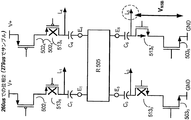
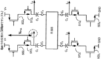
PDACもしくはNDACの出力にかかる測定された電圧が保護帯電圧の外側にあるならば、コンプライアンス電圧V+は、更なる詳細は下で説明するアルゴリズムに従って許容限界内にそのような測定電圧を近づけるように変更される。しかしながら、このアルゴリズムを議論する前に、図10を始めとして出力電圧を測定するために使われた回路の仕様が議論される。大部分は、図10が、(他の構成要素に加えて)コンプライアンス電圧感知制御回路605、スイッチングマトリクス143、少なくとも1つの電圧センサー600、とコンプライアンス電圧調整器610を含む図8の監視回路174の更なる詳細を図解している。この回路、特にスイッチングマトリクス143に給電するのは各電極に関連したラインL175である。与えられた構造では、更に1個以上のカレントソースもしくはカレントシンク回路(例えばカレントミラー)が特定の電極での電流に貢献するだろう。しかしながら、図解が容易なように、ただ1つのソース回路500とシンク回路501が簡略化のため図10に示されている。
If the measured voltage across the output of PDAC or NDAC is outside the guard band voltage, the compliance voltage V + will cause such measured voltages to be brought within acceptable limits according to the algorithm described in more detail below. Be changed. However, prior to discussing this algorithm, the specifications of the circuit used to measure the output voltage are discussed, beginning with FIG. For the most part, the
ラインL 175のタップ点を考えると、ライン上に生じる電圧はソースとシンク回路の出力電圧を示す。示したように、この出力電圧は、ソースとシンク回路502、503の出力トランジスタ(前に述べたように、電流ゲインを拡大縮小するための複数の並列トランジスタを含むことができる)双方にわたる電圧降下と、これらの出力トランジスタを電流に寄与するように選択するために使用される選択トランジスタ513、513にわたる電圧降下を含む。他の実施例ではラインは出力トランジスタ502、503と選択トランジスタ513、513’との間に位置されるのではあるが、これは有益とは考えられない、なぜなら選択トランジスタ513、513’にわたって発生する現実的な電圧降下の監視から排除し得るからである。ライン175は出力電圧の感知に使われる。電極EYでのカレントシンク(NDAC)501にかかる出力電圧は、ラインLNY上の絶対電圧を含
み、これはNDACが接地電圧に参照されるときは、異なる計算を必要とする。一方、電極EXでのカレントソース(PDAC)500にかかる出力電圧はコンプライアンス電圧V+とラインLPXで測定された電圧間の差を含む。
Considering the tap point of
ライン175に対する電圧はスイッチングマトリクス143に提供される。前に述べたように、図10では説明を容易にするためにただ2本のライン175が示されるが、存在する電極の数に依存して更に多くのラインが存在してもよい。1つの実施例において、スイッチングマトリクス143は1本のライン上の電圧を選択し、その電圧(L)を電圧センサー600に表すために使われる。見ることができるように、選択トランジスタ513、513’、スイッチングマトリクス143と電圧センサー600は全てバス606、607そして608経由でコンプライアンス電圧感知制御回路605によって制御される。結局のところ、下記で更に詳細に説明するように、コンプライアンス電圧感知回路605は、様々な測定結果がいつどのように開示されたアルゴリズムと一致させられるかを制御回路174に知らせる、マイクロコントローラ160(図8)からの信号を受信する。
The voltage for
1つの実施例において、電圧センサー600はアナログ電圧“Out”を、示されているようにアナログ−デジタル(A/D)インターフェース635を含むマイクロコントローラ160に出力する。これはマイクロコントローラ160が出力電圧を理解してデジタル処理し、開示されたアルゴリズムに従ってコンプライアンス電圧調整器610(すなわち、最終的にコンプライアンス電圧V+を調節する回路)に制御信号を送ることを可能にする。
In one embodiment,
前に述べたように、ソースもしくはシンク回路を基にしたカレントミラーで望ましいことは、電力が不必要に失われないように、出力トランジスタ502、503がそれほど過度でなく飽和状態で動作することである。したがって、本発明の実施例は出力トランジスタを飽和状態のアクティブカレントソースとシンクに維持するようにコンプライアンス電圧を調整しようとする。カレントソースとカレントシンク回路が負荷を通して直列に接続されること、ゆえにそれらの電流電圧特性に一致して他方と“バランス”をとるように振舞うことを認識すれば、これは常に可能なことではないかもしれない。もし完全な飽和性能がソースとシンクの双方で達成されることができないと、コンプライアンス電圧は最小電力損失によって適切な回路性能を保証するために可能な限り論理的な値に設定されるだろう。
As mentioned earlier, it is desirable for a current mirror based on a source or sink circuit to operate the
図12は分離して見える出力トランジスタ502、503の電流−電圧特性を示している。(更に正確には、シンク501内のN−チャンネル出力トランジスタ503のI−V曲線が示されている。当業者はソース内のP−チャンネル出力トランジスタ502がCMOS回路設計で典型的なように反対の極性を持ち得ることを理解するだろう。)このI−V曲線は飽和電圧Vsatを示し、その上のドレイン−ソース電圧Vdsは飽和状態でトランジスタを動作させるのに充分である。好ましい実施例において、出力トランジスタ502、503が示したような保護帯電圧幅内で動作することが望ましい。保護帯の下限値がVsatを含む一方で、限界を許容するために、また、監視された出力電圧にも含まれるかもしれない、選択トランジスタ513、513’にかかる正常に小さい電圧降下を説明するために、僅かに高い下限値を選ぶことが好まれる。保護帯電圧の上限値は過度でないように選ばれ、出力トランジスタが飽和状態にあるが過度にならないような範囲に限界を定める。好ましい実施例では、カレントソース(PDAC)の保護帯電圧幅は1.5Vから2.1Vで、一方カレントシンク(NDAC)の保護帯電圧幅は1.2Vから1.8Vである。(NDACの下限値は、N−チャンネル出力トランジスタ503が普通、比較可能なPDAC内のP−チャンネル出力トランジスタ502よりも僅かに低い飽和電圧を有していることを反映する。)
FIG. 12 shows the current-voltage characteristics of the
当初に議論したように、図11はIPG100によって利用可能な様々なタイミングチャンネルを示し、どの電極素子が特定時間にカレントソースとシンクとして振舞うかを特定している。タイミングチャンネルAはコンプライアンス電圧調整のための本発明の実施例を説明するために使われる。見ることができるように、チャンネルAにおいて、2つの電極はソースとして振る舞い(E1とE4)、一方2つの電極はシンクとして振舞う(E3とE5)。当初議論されたように、これ以上もしくはこれ以下の電極が電流のソースもしくはシンクとして振舞うことができるが、それぞれ2つのみが例示的なタイミングチャンネルAで説明される。従って設定された、患者の組織を構成する抵抗回路網505を含む例示的な回路はチャンネルAのために図14に示される。承知の通り、様々なソース500とシンク501はIPG100内の個々の電極のために用意されたPDACもしくはNDAC回路(例えば図2Aと2B)から構成されることができ、もしくは当初議論したような他の構造(例えば図3Aから4C)を含むことができる。
As initially discussed, FIG. 11 shows the various timing channels available to the
この例示的なタイミングチャンネル形態と、コンプライアンス電圧V+を監視し最終的に調整するための測定結果のさらなる詳細は、図15A−18Bに関して示される。これらの図のいずれかについても、出力トランジスタ502、503、選択トランジスタ513、513’、抵抗回路網505、各電極に関連したラインLが示されることに注意されたい。図15A、16A、17Aと18Aは、タイミングチャネルAおよび刺激の他の特性(例えば、パルス幅、振幅、周波数、など)によって規定されるように実際の刺激パルスが患者へ配信されている間のソース(PDAC)とシンク(NDAC)回路の形状を示す。したがってこれらの図において、全てのPDACとNDACは回路に結合していることに注意されたい。すなわち、選択トランジスタ513、513’は、各トランジスタに矢印で示されるように全てオンである。また図15A、16A、17A、18Aのそれぞれについて、各電極(VN3A、VN5A、VP1A、VP4A)でのNDACもしくはPDAC回路の出力電圧は、対応したライン(L3、L5、L1、L4)を経由し、NDAC(ラインL3、L5)を最初に始めてPDAC(ラインL1、L4)が続いて、監視されることにも注意されたい。
Further details of this exemplary timing channel configuration and measurement results for monitoring and ultimately adjusting compliance voltage V + are shown with respect to FIGS. 15A-18B. Note that for any of these figures, the
示したように、これらの出力電圧(VN3A、VN5A、VP1A、VP4A)のそれぞれは、L3の出力電圧が最初の刺激期の間に観測され、L5の出力が2番目の刺激期に観測される、などのように、順番に監視されている。しかしながら、連続監視は単一の電圧センサー600(図10)のみを持つ実施例では必要であるが、これらの出力電圧は並行して監視できることに注意すべきである。したがって、もし4個のPDACがカレントソースとして振舞うことができ、1つのタイミングチャンネルの間に4個のNDACがカレントシンクとして振舞うことができると仮定すると、8個の電圧センサー600(示していない)が同時に全ての電圧を感知することを可能にする。この場合、バス607はスイッチングマトリクス143がこれら8個の電圧を8個の異なる電圧センサー600に同時に渡すことを可能にする。
As shown, for each of these output voltages (V N3A , V N5A , V P1A , V P4A ), the L 3 output voltage is observed during the first stimulation period, and the L 5 output is second. It is monitored in order, such as being observed in the stimulation period. However, it should be noted that although continuous monitoring is required in embodiments having only a single voltage sensor 600 (FIG. 10), these output voltages can be monitored in parallel. Thus, assuming that four PDACs can act as current sources and four NDACs can act as current sinks during one timing channel, eight voltage sensors 600 (not shown) Allows to sense all the voltages simultaneously. In this case, the
いづれにしても、前に述べたように、これらライン175によってタップされたNDACとPDACの出力電圧は、スイッチングマトリクス143を経由して電圧センサー600に渡される。その更なる詳細は図13に示す。好ましい実施例において、任意の個々に選ばれたラインLの電圧は差動増幅器625へその電圧を送ることによって推定される。そのような差動増幅器では普通のことだが、参照電圧Vrefも入力である。参照電圧Vrefは、例えば1.2Vのバンドギャップ参照回路を含み得る、参照電圧発生器615によって保持される。参照電圧発生器615は適した値と適した時間にふさわしい参照電圧が作られることを可能にするように、コンプライアンス制御605から渡された、バス614で制御される。
In any event, as mentioned earlier, the output voltages of the NDAC and PDAC tapped by these
最終的に、差動電圧(Out;図10、13)はマイクロコントローラ160のA/D
インターフェース635に送られる。この点について、信号“Out”はNDACおよびPDACにかかる出力電圧の相対値表現であってもよいが、これらの出力電圧の実際の値を含むことはないだろう。それよりも、出力電圧降下の実際の値はマイクロコントローラ160内で計算され得る。例えばそれは、参照電圧Vrefの効果を差し引くことによって、現在設定されているコンプライアンス電圧V+とそのような電圧を比較することなどによって、実際の出力電圧を導き出すかもしれない。別の言い方をすれば、信号“Out”は、単にマイクロコントローラがカレントソースとカレントシンク回路にかかる出力電圧をそこから推定できるような値を、マイクロコントローラ160に知らせる必要があるに過ぎない。もちろん、当業者が承知の通り、出力電圧感知は沢山の別の方法でも起こることができる。例えば、好ましい実施例において感知は参照電圧Vrefに関連して起こるが、感知はコンプライアンス電圧V+、接地、もしくは任意のその他の電圧に関連しても起こり得る。要するに、重要なことはラインL175上の出力電圧が感知されることで、これが具体的に起こる方法は重要ではない。
Finally, the differential voltage (Out; FIGS. 10 and 13) is the A / D of the
It is sent to the
図19と20は、NDAC(図19)とPDAC(図20)双方に対してこれらの出力電圧がどのように推定できるかの実施例をそれぞれ示している。双方の図で、上の3本の跡はIPGの動作とコンプライアンス電圧感知回路を示す信号をあらわす。最初の信号はアクティブな刺激がIPG100内で発生した時を示している。この例に示されているように、その期間は260マイクロ秒であるが、しかしこの長さは、更に下で説明されるように、所定の患者の治療のための特定の刺激パルスの周波数と持続時間に依存して変化することができる。アクティブ刺激期の後、すなわち、260マイクロ秒から開始し、IPGは刺激が発生しない“間期”期間に入る。(間期期間、ならびに電圧監視やコンプライアンス電圧の調整においてそれがどのように使われ得るかは、後で更に詳細に説明する。)
FIGS. 19 and 20 show an example of how these output voltages can be estimated for both NDAC (FIG. 19) and PDAC (FIG. 20), respectively. In both figures, the top three traces represent signals indicating IPG operation and compliance voltage sensing circuitry. The first signal indicates when an active stimulus has occurred in the
図19と20の第二の跡は、アクティブ刺激期の間に出力電圧が監視されたときに命令する制御信号を含む。この第二の形跡の信号は“アクティブ中のサンプル”と呼ばれ、コンプライアンス電圧感知制御回路605(図10と13を見よ)によって送られる1個以上の制御信号を含み得る。示したようにアクティブ信号中のサンプルはセットアップ/サンプル信号を含む。特に、例えば、ライン175上の電圧がスイッチングマトリクス143(図10と13を見よ)を通って通過するのを可能にすることによって、立ち上がりで出力電圧が電圧センサー600を通過することが許可される。アクティブ信号中のサンプルの立下りは、それに反して、電圧センサー600で実際に出力電圧をサンプリングする。説明された詳細な実施例では、このセットアップ/サンプルのスキームのタイプは、出力電圧を適切なレベルに安定させ傾斜させることを可能にするのに役立つ。これは、下で更に議論されるように、整定時間と電圧感知回路のキャパシタンスを考えるとき必要である。そのような電圧沈下は第四と第五の跡で見ることができ、それらはそれぞれNDAC(図19)とPDAC(図20)にかかる出力電圧を示しており、それらの電圧を電力センサー600への入力として示す。見ることができるように、通過電圧が安定することを可能にすることによって、それらは信頼でき、安定した値でサンプリングされることができる。
The second trace of FIGS. 19 and 20 includes control signals that are commanded when the output voltage is monitored during the active stimulation phase. This second evidence signal is referred to as an "active sample" and may include one or more control signals sent by the compliance voltage sense control circuit 605 (see FIGS. 10 and 13). As shown, the samples in the active signal include the setup / sample signal. In particular, for example by allowing the voltage on
図19および図20に示した実施例において、セットアップとサンプリングはアクティブな刺激期間の終わりに向けて、すなわち、それぞれ240および259マイクロ秒において起こる。セットアップとサンプリングは、刺激パルスの終わりに向けて、再び、刺激間の回路の沈下と安定化を可能にするのに役立つ。例えば、結合キャパシタCxがアクティブ刺激期間の間に充電し、それらにかかる電圧はアクティブ刺激パルスの最後において最大であるようになっている。従って、アクティブ刺激期間の終わりに向ってサンプリングが起こることが好ましく、これはコンプライアンス電圧感知がそのようないかなる結合キャパシタ電圧をも明らかにすることを可能にする。更にコンプライアンス電圧V+はア
クティブ刺激間には下垂することがあり得るため、それがその最大にあるとき、これがそのような下垂を考慮するので、アクティブ刺激の終了時近くのサンプリングは更に有益である。その上、刺激終了時近くの感知はまた、電極組織インターフェース上の分極電圧の強化が説明されることを可能にする。
In the example shown in FIGS. 19 and 20, setup and sampling occur towards the end of the active stimulation period, ie, at 240 and 259 microseconds, respectively. Setup and sampling serve to again allow settling and stabilization of the circuit between stimuli towards the end of the stimulation pulse. For example, coupling capacitors C x is charged during the active stimulation period, the voltage applied to them is as is the largest at the end of the active stimulation pulse. Thus, preferably, sampling occurs towards the end of the active stimulation period, which allows compliance voltage sensing to reveal any such coupled capacitor voltage. Furthermore, since the compliance voltage V + can drop between active stimuli, it takes into account such a drop when it is at its maximum, so sampling near the end of the active stimulus is even more useful. Moreover, sensing near the end of stimulation also allows the enhancement of the polarization voltage on the electrode tissue interface to be accounted for.
もちろん、NDACおよびPDACにかかる出力電圧のセットアップおよびサンプリングは沢山の異なる方法で起こることができ、実装特有となるだろう。したがって、電圧センサー600が幾つかの異なる方法で実装できるのと同時に、電圧のサンプリングも使われた実装に依存するだろう。要するに図19および20に示すようなサンプリングと制御信号は単に例示的な実施例の1つだと理解されるだろう。再び、重要な問題点は、NDACおよびPDACにかかる出力電圧が論理時間に監視され、これらの値が、まもなく議論されるコンプライアンス電圧調整アルゴリズムに渡され、それによって処理されることができるということである。
Of course, the setup and sampling of the output voltage across the NDAC and PDAC can occur in many different ways and will be implementation specific. Thus, while
このアルゴリズムの議論をする前に、NDACおよびPDACにかかる出力電圧を測定するためのある代替実施例が議論される。この変形例において、刺激中の出力電圧が測定されるだけでなく、刺激のない期間中の出力電圧も同様に測定される。特に、好ましい実施例において、出力電圧は間期期間内、すなわちアクティブ刺激パルスの間の期間中、に測定される。そのような測定結果は図15B、16B、17B、18Bに示される。それらの図で見られるように、所定のタイミングチャンネル内のそれぞれアクティブなNDACとPDACのための関心のライン上の電圧は、全ての他のDACが切断されている間に監視される。例えば、図15Bにおいて、電極E3に対応した、第一のNDACにかかる電圧が測定され(VN3B)、したがってその選択トランジスタ5133’はオンである。それに反して、全ての他のDACはオフである。すなわち選択トランジスタ5131、5134、5135’はオフである。結果として、コンプライアンス電圧V+と接地間の通り道が中断されるので、患者の肉体を含む抵抗回路網505を通って電流が全く流れないか、もしくは最小の電流が流れる。しかしながら、電極E3のNDACはコンプライアンス電圧V+から切断されていても、NDACが違う方法でオンになるおかげで、いくらかの残りの出力電圧がラインL3上に現れるかもしれない。
Before discussing this algorithm, certain alternative embodiments for measuring the output voltage across the NDAC and PDAC are discussed. In this variant, not only the output voltage during stimulation is measured, but also the output voltage during periods without stimulation. In particular, in a preferred embodiment, the output voltage is measured in an interperiod period, i.e. during the active stimulation pulse. Such measurements are shown in FIGS. 15B, 16B, 17B, 18B. As seen in those figures, the voltage on the line of interest for the respective active NDAC and PDAC in a given timing channel is monitored while all other DACs are disconnected. For example, in FIG 15B, corresponding to the electrodes E 3, the voltage applied to the first NDAC is measured (V N3B), thus the selection transistor 513 3 'is turned on. By contrast, all other DACs are off. That is, the
この間期出力電圧測定結果は、マイクロコントローラ160に処理されるときと、最終的にコンプライアンス電圧調整アルゴリズムによって検討されるとき、出力電圧の精度を改良するために使われることができる。間期出力電圧測定結果(再度、一般的には無視してよいが、潜在的に重要な値)は、任意の特定のDACのアクティブな刺激の測定結果から差し引かれることが好ましい。したがって、図15Aおよび15Bでは、VN3AとVN3Bとして指定された、図16、図17、図18の中の他のDACと同様な、アクティブ(A)と間期(B)の測定結果が電極E3で作られるということに注意されたい。この例の結果は8個の出力電圧測定結果である:VN3A、VN5A、VP1A、VP4Aはアクティブの測定結果、VN3B、VN5B、VP1B、VP4Bは間期の測定結果である。
This interphase output voltage measurement can be used to improve the accuracy of the output voltage as it is processed by the
コンプライアンス電圧調整アルゴリズムで処理されるDACの出力電圧の精度を改良するため、これらの出力アクティブ測定結果と間期測定結果は各DACに対して差し引かれることが望ましい。従って、好ましい実施例では、コンプライアンス電圧調整アルゴリズムに送るための電極E3でのDACにかかる出力電圧はVN3A−VN3Bから構成される。これをすることにより、DAC内の出力トランジスタの動作領域(飽和)の評価は改良されることができ、アクティブDAC自身に起因した残りの電圧は、選択トランジスタ513、513’に起因する電圧降下と同様に、出力電圧測定の外で訂正することができる。
In order to improve the accuracy of the DAC output voltage processed by the compliance voltage adjustment algorithm, it is desirable that these output active and interphase measurements be subtracted for each DAC. Thus, in a preferred embodiment, the output voltage across the DAC at the electrode E 3 for sending to the compliance voltage adjustment algorithm consists of V N3A -V N3B. By doing this, the evaluation of the operating region (saturation) of the output transistor in the DAC can be improved, and the remaining voltage due to the active DAC itself is the voltage drop due to the
間期の出力電圧測定をとることは図19と図20をもう一度参照して示される。特に、第三の跡は“間期間のサンプル”と呼ばれ、間期期間中に出力電圧が監視されたときに命
令する制御信号を含む。この第三の制御信号は前に議論した第二の制御信号(アクティブ中のサンプル)と類似しており、セットアップ/サンプル信号を含む。特に、セットアップ後、立下りは実際に電圧センサーへの入力をサンプリングし、それは再び、そのアクティブな値から安定するための時間を必要とする。図19および図20に示した例において、そのようなサンプリングは279マイクロ秒、すなわち、間期期間中の19マイクロ秒、で起こるが、再び、これらの時間と感知スキームは異なることができ、実装依存である。重要な問題点は、間期の測定がアクティブ測定を補完するものとして使われるべきであり、選ばれた実装と一致した合理的な時間に測定結果をとることであり、またこれは異なる方法で、異なるタイミングに起こることができる。
Taking an interim output voltage measurement is shown once again with reference to FIGS. In particular, the third trace is referred to as a "sample of the interphase" and includes control signals that are commanded when the output voltage is monitored during the interphase. This third control signal is similar to the previously discussed second control signal (active sample) and includes a setup / sample signal. In particular, after setup, falling actually samples the input to the voltage sensor, which again needs time to settle out of its active value. In the example shown in FIGS. 19 and 20, such sampling occurs at 279 microseconds, ie, 19 microseconds during the interphase period, but again, these times and sensing schemes can be different and implemented It is dependent. An important issue is that interphase measurements should be used as a complement to active measurements, taking measurements at reasonable times consistent with the chosen implementation, and this is different , Can occur at different times.
間期の出力電圧の監視が、まさに説明された理由のために有益であり得る一方で、そのような間期の測定結果の使用は全ての有用な実施例において必要とされているわけではない、ということに注意すべきである。それどころか、アクティブ期の測定結果(すなわち、図15A、16A、17A、18Aで図解したもの)のみが使われることができる。前に述べたように、それらのアクティブ出力電圧の測定は同時に行われることができる。一方、間期の測定結果が各DACにかかる不活性出力電圧を測定するために作られるのであれば、そのような測定結果は連続的に、すなわち連続的な間期期間中に、作られる必要があるだろう。 While monitoring of the output voltage of the interphase may be beneficial for the reasons just described, the use of such interphase measurements is not required in all useful embodiments. It should be noted that. Rather, only measurements of the active phase (ie, those illustrated in FIGS. 15A, 16A, 17A, 18A) can be used. As mentioned earlier, measurements of their active output voltage can be made simultaneously. On the other hand, if interphase measurements are made to measure the inactive output voltage across each DAC, such measurements need to be made continuously, ie, during a continuous interphase period. There will be.
好ましい実施例において、特定のタイミングチャンネル内で指定された各アクティブ電極に対する出力電圧の測定結果は、図15A−18Bにおいて指定された順で、連続的にとられる。したがって、シンク電極が最初に測定される:電極E3に関連したNDAC回路がアクティブ刺激中(図15A)に最初に測定され、続いてE3(図15B)の間期(不活性)の測定、その後、E5の同様な測定(図16AとB)、などが行われる。コンプライアンス電圧は下で図21に関して指定されるように、その後調整されることができる。その後、ソース電極は連続して同様に測定される(図17A−18B)。 In the preferred embodiment, the measurement of the output voltage for each active electrode specified in a particular timing channel is taken continuously, in the order specified in FIGS. 15A-18B. Thus, the sink electrode is measured first: the NDAC circuit associated with electrode E 3 is measured first during active stimulation (FIG. 15A), followed by measurement of the phase (inactive) of E 3 (FIG. 15B) , And then similar measurements of E 5 (FIGS. 16A and B), etc. The compliance voltage can then be adjusted as specified below with respect to FIG. After that, the source electrode is continuously measured in the same manner (FIGS. 17A-18B).
実際に処方された治療法との関連で測定結果が作られるので、監視信号のタイミングが調整可能であることが好ましい。この点で、セットアップ/サンプルの測定結果は、刺激パルスとそれらの間の間期期間に適切に"fit"できるように、規定の刺激パルスの周波数と継続時間を考えることは特に重要である。例えば、図19と図20に示された例のための信号のタイミングがある周波数に相応しい一方で、高い周波数はより詰まったタイミングを要求するだろう。 Preferably, the timing of the monitoring signal is adjustable, as the measurement results are made in the context of the therapy actually prescribed. In this regard, it is particularly important to consider the frequency and duration of a given stimulation pulse so that the setup / sample measurements can be properly "fit" to the stimulation pulse and the interphase period between them. For example, while the timing of the signals for the example shown in FIGS. 19 and 20 may be commensurate with a certain frequency, higher frequencies may require tighter timing.
更に、各刺激パルス間で、埋め込み可能な刺激装置では普通のことだが、電荷回復期が続くかもしれない。知っている通り、そのような回復期間は負荷、すなわち組織505、へ注入される電荷を回復するためのパルスを含むことができる。通常、そのような回復は二相性で、アクティブパルスと等しい大きさと継続時間だが逆の極性の回復パルスによって実施される。電荷回復はよく知られているように、受動的にも達成されることができる。そのような電荷回復は簡略化のため図には示していないが、本発明の実施例中では考慮されるだろう。更に、DAC出力電圧は電荷回復期間中に測定されることができることに注意すべきだが、これもまた簡略化のため更には議論しない。
Furthermore, between each stimulation pulse, as is usual with implantable stimulators, a charge recovery phase may continue. As known, such a recovery period can include a load, ie, a pulse to recover the charge injected into the
DACの出力電圧監視の様々な方法を述べてきたが、アルゴリズム的にそれらの電圧がコンプライアンス電圧を有効なレベルに調整するためにどのように使われるのかに注意を向ける。図21に示すように、アルゴリズムは最初に、まさに説明されたように所定のタイミングチャンネルのNDAC(VN1,VN2,...,VNX)の全ての関連出力電圧を得ることから始める。これらの出力電圧はアクティブ刺激(例えば、図15AのVN3A)中に取られた測定結果か、あるいはアクティブと間期の測定結果(例えば、図15Aおよび15BのVN3A−VN3B)間の差として計算された電圧のみを含むことができることを理解
すべきである。普通、そのアルゴリズムはコンプライアンス電圧V+の最小値(例えば、16.8V)で始めるだろうが、もう少し小さい値で始めることができる。
While various methods of DAC output voltage monitoring have been described, algorithmically attention is given to how those voltages are used to adjust the compliance voltage to a valid level. As shown in FIG. 21, the algorithm first begins by obtaining all relevant output voltages of NDACs (V N1 , V N2 ,..., V NX ) of a given timing channel, as just described. These output voltages may be measurements taken during active stimulation (eg, V N3A in FIG. 15A) or differences between active and interphase measurements (eg, V N3A -V N3B in FIGS. 15A and 15B). It should be understood that only the voltages calculated as can be included. Usually, the algorithm will start with the minimum value of compliance voltage V + (e.g. 16.8 V), but can start with a smaller value.
次にNDACの最小出力電圧(Min(VNX))が決定される。この最小出力電圧は、NDACがサブ飽和状態になる危険性が最もあることを示唆し、それ故アルゴリズムのこの実施例においては追跡するのに最も効果的であると考えられる。それ故、アルゴリズムは次に、どのように最小値がNDACの保護帯電圧の幅に対して比較するかを尋ねる。基本的に、もしMin(VNX)がNDACの最大保護帯電圧(例えば、1.8V)より高いと、コンプライアンス電圧V+は減少させられる。なぜなら全てのNDACはこの時点で、電力消費量の見地から最適値になるにはあまりに高過ぎる出力電圧で動作しているということが推察できるからである。示したように、アルゴリズムの反復性質を促進させるために、コンプライアンス電圧V+が減少させられる範囲は、Min(VNX)がNDACの上限保護帯電圧を超える範囲に対応する。したがって、もしMin(VNX)が保護帯を大きく超えている場合(例えばMin(VNX)>4.8V)、コンプライアンス電圧は大きな量(例えば、3.0V)で減少させられる。しかし、もしかろうじて保護帯を超えている(1.8V<Min(VNX)<2.4V)ならば、コンプライアンス電圧は少ない量(例えば、0.6V)で減少させられる。 Next, the minimum NDAC output voltage (Min (V NX )) is determined. This minimum output voltage implies that the NDAC is most at risk of becoming sub-saturated, and is therefore considered to be the most effective to track in this embodiment of the algorithm. Therefore, the algorithm next asks how to compare the minimum value against the width of the guard band voltage of NDAC. Basically, the compliance voltage V + is reduced if Min (V NX ) is higher than NDAC's maximum guard band voltage (eg, 1.8 V). Because it can be inferred at this point that all NDACs are operating at an output voltage that is too high to be optimal from a power consumption standpoint. As indicated, the range over which the compliance voltage V + is reduced corresponds to the range over which Min (V NX ) exceeds the upper guard band voltage of the NDAC, in order to promote the iterative nature of the algorithm. Thus, if Min (V NX ) greatly exceeds the guard band (eg, Min (V NX )> 4.8 V), the compliance voltage is reduced by a large amount (eg, 3.0 V). However, if it is just beyond the protection zone (1.8 V <Min (V NX ) <2.4 V), the compliance voltage is reduced by a small amount (eg, 0.6 V).
結局、コンプライアンス電圧V+が減少させられるとき、NDACにかかる最小電圧降下Min(VNX)は保護帯範囲内(例えば1.2Vと1.8Vの間)になり、PDACがそれから評価されることができる。しかしながら、Min(VNX)が最小保護帯電圧(例えば1.2V)を下回ったならば、コンプライアンス電圧は、PDACの評価よりも前に、例えば0.6Vの増分だけ増加させることができる。もちろん、もしコンプライアンス電圧がこの点で最大値ならば、更にコンプライアンス電圧を増加させることは不可能であり、PDACの評価が開始する。 Eventually, when the compliance voltage V + is reduced, the minimum voltage drop Min (V NX ) across the NDAC will be within the guard band range (eg between 1.2V and 1.8V) and the PDAC will be evaluated from it it can. However, if Min (V NX ) falls below the minimum guard band voltage (eg, 1.2 V), the compliance voltage can be increased by an increment of, for example, 0.6 V prior to the evaluation of the PDAC. Of course, if the compliance voltage is at a maximum at this point, it is not possible to further increase the compliance voltage and evaluation of the PDAC begins.
コンプライアンス電圧V+がNDACに関してこの点で調整されると、アルゴリズムはそのとき、PDACの全ての関連出力電圧(VP1,VP2,...,VPY)を取得する。再び、PDACにかかる最小電圧降下Min(VPY)が決定され、そのときアルゴリズムがNDACと同様に進行する。特に、Min(VPY)がPDACの最大保護帯電圧(例えば2.1V)を超えると、コンプライアンス電圧は最大保護帯電圧からのずれに等しい量で再び減少させられる。 When the compliance voltage V + is adjusted at this point with respect to NDAC, then the algorithm gets all relevant output voltages (V P1 , V P2 ,..., V PY ) of the PDAC. Again, the minimum voltage drop Min (V PY ) across the PDAC is determined, when the algorithm proceeds in the same manner as NDAC. In particular, when Min (V PY ) exceeds the PDAC maximum guard band voltage (eg, 2.1 V), the compliance voltage is again reduced by an amount equal to the deviation from the maximum guard band voltage.
本アルゴリズムのこの点では、たとえNDACにかかる電圧降下の幾つかが最小保護帯電圧に近づいたとしても、コンプライアンス電圧が更に減少することが許容されていることに注意されたい。したがって、もしMin(VPY)が例えば2.1Vを超えると、Min(VNX)が1.8Vを下回り、その他は最適であるときでさえ、V+は減少させることができる。これはNDACをずれて調整するリスクを冒すように思われる一方で、Min(VNX)は双方のDACの電流−電圧特性の効力によってMin(VPY)に関連する(すなわち、釣り合いがとれる)ことに注意されたい。電流はNDACとPDACに対して一致しなければならないので、Min(VPY)が最小PDAC保護帯電圧(例えば、1.5V)を下回ることが無いようにしながら、最小NDAC保護帯しきい値(例えば、1.2V)を著しく下回るようにMin(VNX)を減少させることは難しく、逆もまた同様である。ゆえにこのNDACとPDAC間の釣り合いに起因して、回路性能に影響を与える重要なリスク無しで、すなわち、回路が最適電流を発生させることができないように、コンプライアンス電圧は減らされることができる。 It should be noted that at this point of the algorithm, the compliance voltage is allowed to further decrease even if some of the voltage drop across the NDAC approaches the minimum guard band voltage. Thus, if Min (V PY ) exceeds, for example, 2.1 V, then V min can be reduced, even when Min (V NX ) falls below 1.8 V and others are optimal. While this appears to risk taking the NDAC out of phase, Min (V NX ) is related to Min (V PY ) by the efficacy of the current-voltage characteristics of both DACs (ie, it is balanced). Please note that. Since the current must match for NDAC and PDAC, the minimum NDAC guard band threshold (while ensuring that Min (V PY ) never falls below the minimum PDAC guard voltage (eg, 1.5 V) For example, it is difficult to reduce Min (V NX ) to well below 1.2 V), and vice versa. Therefore, due to this balance between NDAC and PDAC, the compliance voltage can be reduced without significant risk affecting the circuit performance, ie, the circuit can not generate an optimal current.
結局は、コンプライアンス電圧が減らされたとき、PDACにかかる最小出力電圧がPDACの保護帯(1.5<Mic(VPY)<2.1)内にあるのであれば、コンプライアンス電圧は最適であるとみなされる。そうでなければ、PDACがこの点で保護帯を下回
ると、コンプライアンス電圧は(0.6V)の増分だけ増加させることができる。
After all, when the compliance voltage is reduced, the compliance voltage is optimal if the minimum output voltage across the PDAC is within the PDAC's protection band (1.5 <Mic ( VPY ) <2.1). It is considered. Otherwise, when the PDAC falls below the guard band at this point, the compliance voltage can be increased by an increment of (0.6 V).
それ故、この例示的なアルゴリズムの使用を通じて、コンプライアンス電圧は最適値に調整されることができ、その値は適切な回路の性能(すなわち、充分な電流出力)を可能にするために充分高いが、電流出力回路にかかる過度な電圧降下を通じて電力が不要に浪費されないように充分低い。上記が明記したのはそのような2つのカレントソースとシンクの最適化のためのアルゴリズムの1つの実施例ではあるが、他のアルゴリズムが可能であるし、電力が浪費する考察とリスクを心にとどめて、プログラマ特有の好みの影響を受ける。端的に言って、開示されているコンプライアンス電圧アルゴリズムはただ単に実際の刺激の間にNDACとPDACの双方を同時に最適化するための方法を示しただけである。 Therefore, through the use of this exemplary algorithm, the compliance voltage can be adjusted to an optimal value, which is high enough to allow adequate circuit performance (ie sufficient current output) Low enough so that power is not unnecessarily wasted through excessive voltage drop across the current output circuit. Although the above specifies one example of an algorithm for optimization of such two current sources and sinks, other algorithms are possible, keeping in mind the considerations and risks of wasting power. Keep in mind, it is influenced by programmer's specific preferences. In short, the disclosed compliance voltage algorithm merely illustrates a method for simultaneously optimizing both NDAC and PDAC during actual stimulation.
ソース回路とシンク回路にかかる測定された出力電圧は、双方の出力電圧を適切な1つのレベルもしくは複数のレベルにしようとして、コンプライアンス電圧を調整するために使われる一方で、本技術は、また、単に、出力電圧の1つを適当なレベル(例えば、範囲内、特定のポイント、ポイント以上またはポイント以下、など)にさせるために使われることもできることに注意すべきである。したがって、双方の出力電圧が測定されることができ、また他の実施例においては、もちろん双方の電圧を調節することが望ましいが、NDACまたはPDAC出力電圧だけの調整によって利益が得られる。 While the measured output voltages across the source and sink circuits are used to adjust the compliance voltage in an attempt to bring both output voltages to the appropriate level or levels, the technique also It should be noted that it may simply be used to bring one of the output voltages to an appropriate level (e.g., within a range, a particular point, above or below point, etc.). Thus, both output voltages can be measured, and in other embodiments, of course it is desirable to adjust both voltages, but benefits can be obtained by adjusting only the NDAC or PDAC output voltage.
電流の流れる方向は相対的な概念であり、電流が様々なソースに、もしくはソースから流れるかどうかを決定するために、異なる在来技法が使用できることを理解すべきである。この点で、図に電流の流れの方向を表した矢印は、様々な回路の接点への、もしくは接点からの電流の流れを参照したり、電流がシンクされるかソースされるかなどを参照し、全て限定的な意味ではなく、相対的に理解されるべきである。 It should be understood that the direction of current flow is a relative concept, and that different conventional techniques can be used to determine whether current flows to or from various sources. At this point, the arrows that indicate the direction of current flow in the figure refer to the flow of current to or from the contacts of the various circuits, see whether the current is sunk or sourced, etc. And all should be understood relatively, not in a limiting sense.
刺激される組織と隣接している埋め込み可能な“電極”の言及は、埋め込み可能な刺激装置上の電極、または関連した電極リード線、または直接的もしくは間接的に組織を刺激するための任意のその他の構造を含むことも理解すべきである。“電極”はここに開示したようなケース電極も含むことができる。 Reference to an implantable "electrode" adjacent to the tissue to be stimulated refers to an electrode on the implantable stimulator, or an associated electrode lead, or any direct or indirect stimulation of tissue. It should also be understood to include other structures. "Electrodes" can also include case electrodes as disclosed herein.
ここで開示された発明は特定の実施例とその応用を用いて説明されたが、数多くの修正、変更は、請求項で説明された本発明の文言上の均等な範囲を逸脱することなく、当業者により、そこに加えることができる。 Although the invention disclosed herein has been described using specific embodiments and applications thereof, numerous modifications and variations are possible without departing from the scope of the present invention as defined in the claims. It can be added thereto by those skilled in the art.
本発明の上記およびその他の態様は、以下の描画に関連して提示された以下の更に詳細なその記述から更に明白になるだろう。
対応する参照文字は図面のいくつかの図にわたって対応する構成要素を示している。 Corresponding reference characters indicate corresponding components throughout the several views of the drawings.
Claims (15)
前記少なくとも2つの電極間の負荷に少なくとも1つの刺激パルスを供給するステップであって、少なくとも1つの電極はソース回路に結合され、少なくとも1つの電極はシンク回路に結合されることを特徴とするステップと、
前記少なくとも1つの刺激パルスの間に、前記ソース回路にかかる出力電圧を測定するステップと、前記シンク回路にかかる出力電圧を測定するステップと、
前記出力電圧の少なくとも1つを適正レベルにしようとして、前記コンプライアンス電圧を調整するために前記ソース回路と前記シンク回路にかかる前記測定された出力電圧を使うステップ、
とを含む方法。 A method for adjusting a compliance voltage of a stimulator, the device comprising at least one source circuit coupled to the compliance voltage, at least one sink circuit coupled to a reference voltage, and at least two electrodes. Including
Delivering at least one stimulation pulse to a load between the at least two electrodes, wherein the at least one electrode is coupled to a source circuit and the at least one electrode is coupled to a sink circuit When,
Measuring the output voltage across the source circuit during the at least one stimulation pulse; measuring the output voltage across the sink circuit;
Using the measured output voltage across the source circuit and the sink circuit to adjust the compliance voltage in an attempt to bring at least one of the output voltages to a proper level;
And how to contain it.
コンプライアンス電圧に結合された少なくとも1つのソース回路と、参照電圧に結合された少なくとも1つのシンク回路であって、各ソース回路は関連したソース電極に関連した第一スイッチ経由で結合され、各シンク回路は関連したシンク電極に関連した第二スイッチ経由で結合されることを特徴とする、コンプライアンス電圧に結合された少なくとも1つのソース回路と、参照電圧に結合された少なくとも1つのシンク回路と、
各アクティブなソースもしくはシンク電極に結合された各ソースもしくはシンク回路の出力電圧を示す電圧をラインに沿って受け取るための電圧センサー回路と、
を含む刺激装置。 At least two electrodes for stimulating tissue, wherein the at least two electrodes are programmable to be active at a predetermined time, and at least one of the active electrodes comprises a source electrode, At least two electrodes for stimulating tissue, characterized in that at least one of the active electrodes comprises a sink electrode;
At least one source circuit coupled to the compliance voltage and at least one sink circuit coupled to the reference voltage, each source circuit coupled via a first switch associated with an associated source electrode, each sink circuit And at least one source circuit coupled to the compliance voltage, and at least one sink circuit coupled to the reference voltage, wherein the at least one source circuit is coupled to the compliance voltage, wherein
A voltage sensor circuit for receiving along the line a voltage indicative of an output voltage of each source or sink circuit coupled to each active source or sink electrode;
Stimulation device.
うかを決めるための、論理回路と、
前記論理回路の出力を受け取るためと、もし前記決定された出力電圧が前記適正レベルでない場合に前記コンプライアンス電圧を調整するための、調整回路と
を更に含む、請求項9記載の刺激装置。 Logic circuitry to receive the output of the voltage sensor circuit and to determine if the output voltage is at the proper level;
10. The stimulator of claim 9, further comprising: adjusting circuitry to receive the output of the logic circuitry and to adjust the compliance voltage if the determined output voltage is not at the proper level.
Applications Claiming Priority (3)
| Application Number | Priority Date | Filing Date | Title |
|---|---|---|---|
| US11/305,898 US7444181B2 (en) | 2005-12-14 | 2005-12-14 | Techniques for sensing and adjusting a compliance voltage in an implantable stimulator device |
| US11/305,898 | 2005-12-14 | ||
| PCT/US2006/060085 WO2007070727A1 (en) | 2005-12-14 | 2006-10-19 | Techniques for sensing and adjusting a compliance voltage in an implantable stimulator device |
Publications (2)
| Publication Number | Publication Date |
|---|---|
| JP2009519771A true JP2009519771A (en) | 2009-05-21 |
| JP4856718B2 JP4856718B2 (en) | 2012-01-18 |
Family
ID=37836716
Family Applications (1)
| Application Number | Title | Priority Date | Filing Date |
|---|---|---|---|
| JP2008545891A Expired - Fee Related JP4856718B2 (en) | 2005-12-14 | 2006-10-19 | Techniques for sensing and adjusting the compliance voltage of an implantable stimulator |
Country Status (6)
| Country | Link |
|---|---|
| US (5) | US7444181B2 (en) |
| EP (1) | EP1962950B1 (en) |
| JP (1) | JP4856718B2 (en) |
| CA (1) | CA2632638A1 (en) |
| ES (1) | ES2587367T3 (en) |
| WO (1) | WO2007070727A1 (en) |
Cited By (12)
| Publication number | Priority date | Publication date | Assignee | Title |
|---|---|---|---|---|
| JP2012532672A (en) * | 2009-07-08 | 2012-12-20 | ネヴロ コーポレイション | System and method for adjusting electrotherapy based on changes in impedance |
| JP2013540021A (en) * | 2010-10-13 | 2013-10-31 | ボストン サイエンティフィック ニューロモデュレイション コーポレイション | Sample and hold circuit for monitoring voltage in an implantable neurostimulator |
| JP2013540020A (en) * | 2010-10-13 | 2013-10-31 | ボストン サイエンティフィック ニューロモデュレイション コーポレイション | Electrode voltage monitoring in implantable medical device systems with daisy chain electrode-driver integrated circuits |
| US9199083B2 (en) | 2009-02-10 | 2015-12-01 | Nevro Corporation | Systems and methods for delivering neural therapy correlated with patient status |
| US9295840B1 (en) | 2013-01-22 | 2016-03-29 | Nevro Corporation | Systems and methods for automatically programming patient therapy devices |
| US9409019B2 (en) | 2009-07-28 | 2016-08-09 | Nevro Corporation | Linked area parameter adjustment for spinal cord stimulation and associated systems and methods |
| JP2016529039A (en) * | 2013-08-29 | 2016-09-23 | ボストン サイエンティフィック ニューロモデュレイション コーポレイション | System and method for adjusting compliance voltage of neuromodulation device |
| US9517344B1 (en) | 2015-03-13 | 2016-12-13 | Nevro Corporation | Systems and methods for selecting low-power, effective signal delivery parameters for an implanted pulse generator |
| US9731133B1 (en) | 2013-01-22 | 2017-08-15 | Nevro Corp. | Systems and methods for systematically testing a plurality of therapy programs in patient therapy devices |
| US9814884B2 (en) | 2011-11-04 | 2017-11-14 | Nevro Corp. | Systems and methods for detecting faults and/or adjusting electrical therapy based on impedance changes |
| US9895538B1 (en) | 2013-01-22 | 2018-02-20 | Nevro Corp. | Systems and methods for deploying patient therapy devices |
| US10300277B1 (en) | 2015-12-14 | 2019-05-28 | Nevro Corp. | Variable amplitude signals for neurological therapy, and associated systems and methods |
Families Citing this family (158)
| Publication number | Priority date | Publication date | Assignee | Title |
|---|---|---|---|---|
| JP4423453B2 (en) * | 2005-05-25 | 2010-03-03 | エルピーダメモリ株式会社 | Semiconductor memory device |
| US7444181B2 (en) * | 2005-12-14 | 2008-10-28 | Boston Scientific Neuromodulation Corporation | Techniques for sensing and adjusting a compliance voltage in an implantable stimulator device |
| US8014866B2 (en) * | 2006-07-13 | 2011-09-06 | Cardiac Pacemakers, Inc. | Variable voltage compliance for current output generator |
| US20080103572A1 (en) | 2006-10-31 | 2008-05-01 | Medtronic, Inc. | Implantable medical lead with threaded fixation |
| US8010205B2 (en) | 2007-01-11 | 2011-08-30 | Boston Scientific Neuromodulation Corporation | Multiple telemetry and/or charging coil configurations for an implantable medical device system |
| WO2008112178A1 (en) | 2007-03-09 | 2008-09-18 | Dan Sachs | Muscle stimulator |
| US11679261B2 (en) | 2007-03-09 | 2023-06-20 | Mainstay Medical Limited | Systems and methods for enhancing function of spine stabilization muscles associated with a spine surgery intervention |
| US9072897B2 (en) | 2007-03-09 | 2015-07-07 | Mainstay Medical Limited | Systems and methods for restoring muscle function to the lumbar spine |
| US10925637B2 (en) * | 2010-03-11 | 2021-02-23 | Mainstay Medical Limited | Methods of implanting electrode leads for use with implantable neuromuscular electrical stimulator |
| US11679262B2 (en) | 2007-03-09 | 2023-06-20 | Mainstay Medical Limited | Systems and methods for restoring muscle function to the lumbar spine |
| US11331488B2 (en) | 2007-03-09 | 2022-05-17 | Mainstay Medical Limited | Systems and methods for enhancing function of spine stabilization muscles associated with a spine surgery intervention |
| US8649858B2 (en) * | 2007-06-25 | 2014-02-11 | Boston Scientific Neuromodulation Corporation | Architectures for an implantable medical device system |
| US20090069869A1 (en) * | 2007-09-11 | 2009-03-12 | Advanced Bionics Corporation | Rotating field inductive data telemetry and power transfer in an implantable medical device system |
| US20090132009A1 (en) * | 2007-11-21 | 2009-05-21 | Medtronic, Inc. | Determination of stimulation output capabilities throughout power source voltage range |
| US20090265042A1 (en) * | 2008-04-17 | 2009-10-22 | Mollenkopf James D | System and Method for Providing Voltage Regulation in a Power Distribution System |
| US8653648B2 (en) * | 2008-10-03 | 2014-02-18 | Taiwan Semiconductor Manufacturing Company, Ltd. | Zigzag pattern for TSV copper adhesion |
| US7818060B2 (en) | 2008-10-31 | 2010-10-19 | Medtronic, Inc. | Determination of stimulation output capabilities throughout power source voltage range |
| US8219196B2 (en) * | 2008-10-31 | 2012-07-10 | Medtronic, Inc. | Determination of stimulation output capabilities throughout power source voltage range |
| JP2012508624A (en) * | 2008-11-13 | 2012-04-12 | プロテウス バイオメディカル インコーポレイテッド | Multiplexed multiple electrode nerve stimulator |
| WO2010056438A2 (en) | 2008-11-13 | 2010-05-20 | Proteus Biomedical, Inc. | Shielded stimulation and sensing system and method |
| US9233254B2 (en) | 2009-02-17 | 2016-01-12 | Boston Scientific Neuromodulation Corporation | Selectable boost converter and charge pump for compliance voltage generation in an implantable stimulator device |
| US20100268309A1 (en) | 2009-04-17 | 2010-10-21 | Boston Scientific Neuromodulation Corporation | Architectures for Multi-Electrode Implantable Stimulator Devices Having Minimal Numbers of Decoupling Capacitors |
| US8321029B2 (en) | 2009-09-18 | 2012-11-27 | Boston Scientific Neuromodulation Corporation | External charger usable with an implantable medical device having a programmable or time-varying temperature set point |
| AU2009217394A1 (en) | 2009-09-18 | 2011-04-07 | Cochlear Limited | A Method Of Calibrating Current Sources And Current Sinks In A Multi-Electrode Stimulation System |
| AU2009222439B2 (en) * | 2009-09-28 | 2011-07-21 | Cochlear Limited | Method and circuitry for measurement and control of stimulation current |
| ES2562451T3 (en) * | 2009-09-29 | 2016-03-04 | Yeditepe Universitesi | Power management techniques for implanted stimulators |
| US9415223B2 (en) * | 2009-11-02 | 2016-08-16 | Boston Scientific Neuromodulation Corporation | Charge recovery bi-phasic control for tissue stimulation |
| US9539430B2 (en) * | 2009-12-29 | 2017-01-10 | Advanced Bionics Ag | Dynamic compliance voltage management for an implantable stimulator |
| US11786725B2 (en) | 2012-06-13 | 2023-10-17 | Mainstay Medical Limited | Systems and methods for restoring muscle function to the lumbar spine and kits for implanting the same |
| US9950159B2 (en) | 2013-10-23 | 2018-04-24 | Mainstay Medical Limited | Systems and methods for restoring muscle function to the lumbar spine and kits for implanting the same |
| CA2792529C (en) | 2010-03-11 | 2018-06-05 | Mainstay Medical, Inc. | Modular stimulator for treatment of back pain, implantable rf ablation system and methods of use |
| US11684774B2 (en) | 2010-03-11 | 2023-06-27 | Mainstay Medical Limited | Electrical stimulator for treatment of back pain and methods of use |
| US12097365B2 (en) | 2010-03-11 | 2024-09-24 | Mainstay Medical Limited | Electrical stimulator for the treatment of back pain and methods of use |
| US9999763B2 (en) | 2012-06-13 | 2018-06-19 | Mainstay Medical Limited | Apparatus and methods for anchoring electrode leads adjacent to nervous tissue |
| US9155891B2 (en) * | 2010-09-20 | 2015-10-13 | Neuropace, Inc. | Current management system for a stimulation output stage of an implantable neurostimulation system |
| EP2627404B1 (en) | 2010-10-13 | 2017-12-13 | Boston Scientific Neuromodulation Corporation | Architectures for an implantable medical device system having daisy-chained electrode-drive integrated circuits |
| WO2012061608A2 (en) | 2010-11-03 | 2012-05-10 | The Cleveland Clinic Foundation | Apparatus for energy efficient stimulation |
| WO2012068247A1 (en) | 2010-11-16 | 2012-05-24 | The Board Of Trustees Of The Leland Stanford Junior University | Systems and methods for treatment of dry eye |
| US9821159B2 (en) | 2010-11-16 | 2017-11-21 | The Board Of Trustees Of The Leland Stanford Junior University | Stimulation devices and methods |
| CN105727444B (en) * | 2011-04-07 | 2018-10-09 | 奥库利维公司 | Stimulating apparatus |
| US8515545B2 (en) | 2011-04-29 | 2013-08-20 | Greatbatch Ltd. | Current steering neurostimulator device with unidirectional current sources |
| US9101767B2 (en) | 2011-05-18 | 2015-08-11 | Greatbatch Ltd. | Measuring load impedance with active stimulation pulses in an implanted pulse generator |
| US8571667B2 (en) * | 2011-07-01 | 2013-10-29 | Greatbatch Ltd. | Active current control using the enclosure of an implanted pulse generator |
| AU2012286590B2 (en) | 2011-07-28 | 2014-09-18 | The Bionics Institute Of Australia | Device and circuitry for controlling delivery of stimulation signals |
| AU2012290152B2 (en) | 2011-08-02 | 2016-08-11 | Mainstay Medical Limited | Apparatus for anchoring electrode leads for use with implantable neuromuscular electrical stimulator |
| US8666504B2 (en) | 2011-10-24 | 2014-03-04 | Boston Scientific Neuromodulation Corporation | Communication and charging circuitry for a single-coil implantable medical device |
| US20130110203A1 (en) | 2011-10-27 | 2013-05-02 | Boston Scientific Neuromodulation Corporation | Managing a Multi-function Coil in an Implantable Medical Device Using an Optical Switch |
| EP2773423B1 (en) | 2011-11-04 | 2024-01-10 | Nevro Corporation | Medical device communication and charding assemblies for use with implantable signal generators |
| CA2858824C (en) | 2011-12-19 | 2020-05-26 | Mainstay Medical Limited | Apparatus for rehabilitating a muscle and assessing progress of rehabilitation |
| US20130184794A1 (en) | 2012-01-16 | 2013-07-18 | Boston Scientific Neuromodulation Corporation | Architectures for an Implantable Stimulator Device Having a Plurality of Electrode Driver Integrated Circuits with Shorted Electrode Outputs |
| US9186520B2 (en) | 2012-01-16 | 2015-11-17 | Boston Scientific Neuromodulation Corporation | Automatic on-off charger for an implantable medical device |
| WO2013111137A2 (en) | 2012-01-26 | 2013-08-01 | Rainbow Medical Ltd. | Wireless neurqstimulatqrs |
| US9002465B2 (en) | 2012-04-06 | 2015-04-07 | Boston Scientific Neuromodulation Corporation | Verifying correct operation of an implantable neurostimulator device using current distribution circuitry |
| EP2841152A1 (en) | 2012-04-27 | 2015-03-04 | Boston Scientific Neuromodulation Corporation | Timing channel circuitry for creating pulses in an implantable stimulator device |
| US9174051B2 (en) | 2012-04-29 | 2015-11-03 | Boston Scientific Neuromodulation Corporation | Real time compliance voltage generation for an implantable stimulator |
| US9314632B2 (en) | 2012-05-17 | 2016-04-19 | Boston Scientific Neuromodulation Corporation | Pulse-by-pulse compliance voltage generation for an implantable stimulator |
| SG195499A1 (en) * | 2012-05-22 | 2013-12-30 | Agency Science Tech & Res | Stimulator and method for processing a stimulation signal |
| US10327810B2 (en) | 2016-07-05 | 2019-06-25 | Mainstay Medical Limited | Systems and methods for enhanced implantation of electrode leads between tissue layers |
| US10195419B2 (en) | 2012-06-13 | 2019-02-05 | Mainstay Medical Limited | Electrode leads for use with implantable neuromuscular electrical stimulator |
| US9186501B2 (en) | 2012-06-13 | 2015-11-17 | Mainstay Medical Limited | Systems and methods for implanting electrode leads for use with implantable neuromuscular electrical stimulator |
| CN104662787B (en) | 2012-08-31 | 2017-08-25 | 艾尔弗雷德·E·曼科学研究基金会 | The feedback control coil actuator transmitted for induction power |
| US9861812B2 (en) | 2012-12-06 | 2018-01-09 | Blue Wind Medical Ltd. | Delivery of implantable neurostimulators |
| US9717627B2 (en) | 2013-03-12 | 2017-08-01 | Oculeve, Inc. | Implant delivery devices, systems, and methods |
| AU2014232252B2 (en) | 2013-03-15 | 2018-01-18 | Alfred E. Mann Foundation For Scientific Research | Current sensing multiple output current stimulators with fast turn on time |
| US9440076B2 (en) | 2013-03-15 | 2016-09-13 | Globus Medical, Inc. | Spinal cord stimulator system |
| US9872997B2 (en) | 2013-03-15 | 2018-01-23 | Globus Medical, Inc. | Spinal cord stimulator system |
| US9887574B2 (en) | 2013-03-15 | 2018-02-06 | Globus Medical, Inc. | Spinal cord stimulator system |
| JP6174781B2 (en) | 2013-03-15 | 2017-08-02 | アルフレッド イー. マン ファウンデーション フォー サイエンティフィック リサーチ | Successive approximation analog-to-digital converter for high voltage monitoring |
| US9878170B2 (en) | 2013-03-15 | 2018-01-30 | Globus Medical, Inc. | Spinal cord stimulator system |
| EP2790470B1 (en) | 2013-04-08 | 2018-03-21 | Dialog Semiconductor GmbH | Programmable current source with optimized compliance region for efficient backlighting in portable applications |
| WO2014172693A2 (en) | 2013-04-19 | 2014-10-23 | Oculeve, Inc. | Nasal stimulation devices and methods |
| AU2014262150B2 (en) | 2013-05-03 | 2019-02-07 | Alfred E. Mann Foundation For Scientific Research | High reliability wire welding for implantable devices |
| JP6513638B2 (en) | 2013-05-03 | 2019-05-15 | アルフレッド イー. マン ファウンデーション フォー サイエンティフィック リサーチ | Multi-branch stimulation electrode for subcutaneous area stimulation |
| WO2014179685A1 (en) | 2013-05-03 | 2014-11-06 | Nevro Corporation | Molded headers for implantable signal generators, and associated systems and methods |
| CN105658276B (en) | 2013-05-03 | 2018-10-02 | 艾尔弗雷德·E·曼科学研究基金会 | Implantation material recharger is shaken hands system and method |
| US20150018911A1 (en) | 2013-07-02 | 2015-01-15 | Greatbatch Ltd. | Apparatus, system, and method for minimized energy in peripheral field stimulation |
| CN105264736B (en) | 2013-07-29 | 2017-05-10 | 艾尔弗雷德·E·曼科学研究基金会 | Implant charging field control through radio link |
| JP6503351B2 (en) | 2013-07-29 | 2019-04-17 | アルフレッド イー. マン ファウンデーション フォー サイエンティフィック リサーチ | High efficiency magnetic link for implantable devices |
| CA3075310C (en) | 2013-07-29 | 2022-04-05 | Alfred E. Mann Foundation For Scientific Research | Microprocessor controlled class e driver |
| US9238141B2 (en) * | 2013-08-15 | 2016-01-19 | Medtronic, Inc. | Devices and methods to provide stimulation therapy in the presence of external conditions that induce undesirable perturbations |
| US9364673B2 (en) | 2013-10-16 | 2016-06-14 | Boston Scientific Neuromodulation Corporation | Power supply disconnect current measurement for an implantable medical device |
| US9643007B2 (en) | 2013-10-30 | 2017-05-09 | Advanced Bionics Ag | Utilization of different loudness encoding schemes in cochlear implant systems |
| WO2015126432A1 (en) * | 2014-02-24 | 2015-08-27 | Advanced Bionics Ag | Systems and methods for detecting a compliance state of a current source included in a cochlear implant |
| CN111298285A (en) | 2014-02-25 | 2020-06-19 | 奥库利维公司 | Polymer formulations for nasolacrimal stimulation |
| EP3903875A1 (en) | 2014-05-20 | 2021-11-03 | Nevro Corporation | Implanted pulse generators with reduced power consumption via signal strength/duration characteristics, and associated systems and methods |
| EP3791922B1 (en) | 2014-07-10 | 2025-04-02 | Curonix LLC | Circuit for an implantable device |
| FR3024305B1 (en) * | 2014-07-23 | 2018-03-30 | Devialet | INPUT STAGE OF AN AMPLIFIER AND CORRESPONDING AMPLIFIER |
| CA2956176A1 (en) | 2014-07-25 | 2016-01-28 | Oculeve, Inc. | Stimulation patterns for treating dry eye |
| CA3208375A1 (en) | 2014-08-15 | 2016-02-18 | Axonics, Inc. | External pulse generator device and associated methods for trial nerve stimulation |
| CA2957967C (en) | 2014-08-15 | 2018-11-27 | Axonics Modulation Technologies, Inc. | Systems and methods for neurostimulation electrode configurations based on neural localization |
| CA2958199C (en) | 2014-08-15 | 2023-03-07 | Axonics Modulation Technologies, Inc. | Electromyographic lead positioning and stimulation titration in a nerve stimulation system for treatment of overactive bladder |
| US10682521B2 (en) | 2014-08-15 | 2020-06-16 | Axonics Modulation Technologies, Inc. | Attachment devices and associated methods of use with a nerve stimulation charging device |
| WO2016025915A1 (en) | 2014-08-15 | 2016-02-18 | Axonics Modulation Technologies, Inc. | Integrated electromyographic clinician programmer for use with an implantable neurostimulator |
| EP3180070B1 (en) | 2014-08-15 | 2021-04-14 | Axonics Modulation Technologies, Inc. | Implantable lead affixation structure for nerve stimulation to alleviate bladder dysfunction and other indications |
| US10471268B2 (en) | 2014-10-16 | 2019-11-12 | Mainstay Medical Limited | Systems and methods for monitoring muscle rehabilitation |
| WO2016065211A1 (en) | 2014-10-22 | 2016-04-28 | Oculeve, Inc. | Contact lens for increasing tear production |
| MX2017005204A (en) | 2014-10-22 | 2017-12-14 | Oculeve Inc | Stimulation devices and methods for treating dry eye. |
| WO2016065213A1 (en) | 2014-10-22 | 2016-04-28 | Oculeve, Inc. | Implantable nasal stimulator systems and methods |
| AU2015336218B2 (en) | 2014-10-22 | 2020-07-23 | Nevro Corp. | Systems and methods for extending the life of an implanted pulse generator battery |
| CN104548341A (en) * | 2014-12-20 | 2015-04-29 | 江门百脉医疗器械有限公司 | Performance detection method of micro-current stimulator |
| CA2973192C (en) | 2015-01-09 | 2023-04-04 | Axonics Modulation Technologies, Inc. | Improved antenna and methods of use for an implantable nerve stimulator |
| JP6751718B2 (en) | 2015-01-09 | 2020-09-09 | アクソニクス モジュレーション テクノロジーズ インコーポレイテッド | Mounting devices and related methods for use with neurostimulation charging devices |
| JP6805153B2 (en) | 2015-01-09 | 2020-12-23 | アクソニクス モジュレーション テクノロジーズ インコーポレイテッド | How to use with patient remote devices and associated neurostimulation systems |
| US9739809B2 (en) | 2015-02-06 | 2017-08-22 | Cactus Semiconductor, Inc. | Compliance voltage detector circuit |
| US9867994B2 (en) | 2015-06-19 | 2018-01-16 | Boston Scientific Neuromodulation Corporation | External powering of implantable medical device dependent on energy of provided therapy |
| JP6946261B2 (en) | 2015-07-10 | 2021-10-06 | アクソニクス インコーポレイテッド | Implantable nerve stimulators and methods with internal electronics without ASICs |
| US11318310B1 (en) | 2015-10-26 | 2022-05-03 | Nevro Corp. | Neuromodulation for altering autonomic functions, and associated systems and methods |
| US10105540B2 (en) | 2015-11-09 | 2018-10-23 | Bluewind Medical Ltd. | Optimization of application of current |
| US10576292B2 (en) | 2015-11-29 | 2020-03-03 | Boston Scientific Neuromodulation Corporation | Skull-mounted deep brain stimulator |
| US10420950B2 (en) | 2015-11-29 | 2019-09-24 | Boston Scientific Neuromodulation Corporation | Implantable pulse generator usable during a trial stimulation phase and externally powered by magnetic inductive coupling |
| US10426958B2 (en) | 2015-12-04 | 2019-10-01 | Oculeve, Inc. | Intranasal stimulation for enhanced release of ocular mucins and other tear proteins |
| AU2016382867B2 (en) * | 2015-12-31 | 2021-12-23 | Nevro Corp. | Controller for nerve stimulation circuit and associated systems and methods |
| US10195423B2 (en) | 2016-01-19 | 2019-02-05 | Axonics Modulation Technologies, Inc. | Multichannel clip device and methods of use |
| US9517338B1 (en) | 2016-01-19 | 2016-12-13 | Axonics Modulation Technologies, Inc. | Multichannel clip device and methods of use |
| US10603500B2 (en) | 2016-01-29 | 2020-03-31 | Axonics Modulation Technologies, Inc. | Methods and systems for frequency adjustment to optimize charging of implantable neurostimulator |
| EP3413970B1 (en) | 2016-02-12 | 2021-06-30 | Axonics, Inc. | External pulse generator device for trial nerve stimulation |
| US10252048B2 (en) | 2016-02-19 | 2019-04-09 | Oculeve, Inc. | Nasal stimulation for rhinitis, nasal congestion, and ocular allergies |
| US10615802B2 (en) | 2016-03-18 | 2020-04-07 | The Governing Council Of The University Of Toronto | Dynamic parameter operation of an FPGA |
| US20170272073A1 (en) * | 2016-03-18 | 2017-09-21 | Altera Corporation | Dynamic parameter operation of an fpga |
| WO2017192572A1 (en) | 2016-05-02 | 2017-11-09 | Oculeve, Inc. | Intranasal stimulation for treatment of meibomian gland disease and blepharitis |
| US11040192B2 (en) | 2016-09-10 | 2021-06-22 | Boston Scientific Neuromodulation Corporation | Current generation architecture for an implantable medical device |
| US10549091B2 (en) | 2016-09-10 | 2020-02-04 | Boston Scientific Neuromodulation Corporation | Use models for a current generation architecture for an implantable medical device |
| US10632300B2 (en) | 2016-09-10 | 2020-04-28 | Boston Scientific Neuromodulation Corporation | Measurement circuitry for measuring analog values in an implantable pulse generator |
| US10716932B2 (en) | 2016-09-10 | 2020-07-21 | Boston Scientific Neuromodulation Corporation | Pulse definition circuitry for creating stimulation waveforms in an implantable pulse generator |
| US10525252B2 (en) * | 2016-09-10 | 2020-01-07 | Boston Scientific Neuromodulation Corporation | Compliance voltage monitoring and adjustment in an implantable medical device |
| US10589090B2 (en) | 2016-09-10 | 2020-03-17 | Boston Scientific Neuromodulation Corporation | Implantable stimulator device with magnetic field sensing circuit |
| US10716937B2 (en) | 2016-09-10 | 2020-07-21 | Boston Scientific Neuromodulation Corporation | Passive charge recovery circuitry for an implantable medical device |
| US10786665B2 (en) * | 2016-09-10 | 2020-09-29 | Boston Scientific Neuromodulation Corporation | Biasing of a current generation architecture for an implantable medical device |
| US20180071515A1 (en) | 2016-09-10 | 2018-03-15 | Boston Scientific Neuromodulation Corporation | Pulse Definition Circuitry for Creating Stimulation Waveforms in an Implantable Pulse Generator |
| US10576265B2 (en) | 2016-09-10 | 2020-03-03 | Boston Scientific Neuromodulation Corporation | Pulse definition circuitry for creating stimulation waveforms in an implantable pulse generator |
| US10525253B2 (en) | 2016-10-13 | 2020-01-07 | Boston Scientific Neuromodulation Corporation | Current generation architecture for an implantable medical device including controllable slew rate |
| US10525264B2 (en) | 2016-11-16 | 2020-01-07 | Samsung Electronics Co., Ltd. | Stimulator and method of controlling stimulator |
| US10124178B2 (en) | 2016-11-23 | 2018-11-13 | Bluewind Medical Ltd. | Implant and delivery tool therefor |
| CA3045018A1 (en) | 2016-12-02 | 2018-06-07 | Oculeve, Inc. | Apparatus and method for dry eye forecast and treatment recommendation |
| US20180353764A1 (en) | 2017-06-13 | 2018-12-13 | Bluewind Medical Ltd. | Antenna configuration |
| US10780285B2 (en) | 2017-09-15 | 2020-09-22 | Boston Scientific Neuromodulation Corporation | Current generation architecture for an implantable stimulator device including distributor circuitry for sending an amplitude-scaled current to digital-to-analog converters at the electrodes |
| AU2018222994B2 (en) | 2017-09-15 | 2019-11-07 | Boston Scientific Neuromodulation Corporation | Current generation architecture for an implantable stimulator device to promote current steering between electrodes |
| CR20200357A (en) | 2018-01-30 | 2021-03-29 | Nevro Corp | Efficient use of an implantable pulse generator battery, and associated systems and methods |
| DE102018129587A1 (en) | 2018-02-19 | 2019-08-22 | Biotronik Se & Co. Kg | Systems and methods for simultaneous stimulation by multiple electrodes |
| US11110283B2 (en) | 2018-02-22 | 2021-09-07 | Axonics, Inc. | Neurostimulation leads for trial nerve stimulation and methods of use |
| US11040202B2 (en) | 2018-03-30 | 2021-06-22 | Boston Scientific Neuromodulation Corporation | Circuitry to assist with neural sensing in an implantable stimulator device |
| US11590352B2 (en) | 2019-01-29 | 2023-02-28 | Nevro Corp. | Ramped therapeutic signals for modulating inhibitory interneurons, and associated systems and methods |
| US10933238B2 (en) | 2019-01-31 | 2021-03-02 | Nevro Corp. | Power control circuit for sterilized devices, and associated systems and methods |
| WO2020185902A1 (en) | 2019-03-11 | 2020-09-17 | Axonics Modulation Technologies, Inc. | Charging device with off-center coil |
| US11565117B2 (en) | 2019-05-02 | 2023-01-31 | Boston Scientific Neuromodulation Corporation | Amplitude modulating waveform pattern generation for stimulation in an implantable pulse generator |
| US11439829B2 (en) | 2019-05-24 | 2022-09-13 | Axonics, Inc. | Clinician programmer methods and systems for maintaining target operating temperatures |
| US11848090B2 (en) | 2019-05-24 | 2023-12-19 | Axonics, Inc. | Trainer for a neurostimulator programmer and associated methods of use with a neurostimulation system |
| CN113924038B (en) * | 2019-06-28 | 2024-05-14 | 领先仿生公司 | Temperature sensing architecture for implantable devices |
| AU2020340952B2 (en) * | 2019-09-06 | 2023-11-09 | Boston Scientific Neuromodulation Corporation | Management of compliance voltage for a stimulator device |
| AU2021231494B2 (en) * | 2020-03-03 | 2024-05-09 | Boston Scientific Neuromodulation Corporation | Digital-to-analog converter circuitry for a stimulator device having non-linear amplitude adjustment |
| US12420103B1 (en) | 2020-08-20 | 2025-09-23 | Axonics, Inc. | Neurostimulation leads with reduced current leakage |
| US12527959B2 (en) | 2020-11-20 | 2026-01-20 | Boston Scientific Neuromodulation Corporation | Compliance voltage monitoring and adjustment in an implantable medical device using low side sensing |
| US11826577B2 (en) * | 2021-02-25 | 2023-11-28 | Medtronic, Inc. | Impedance measurement circuit architecture |
| WO2022217184A1 (en) | 2021-04-06 | 2022-10-13 | Boston Scientific Neuromodulation Corporation | Current generation architecture for an implantable stimulator device |
| US11400299B1 (en) | 2021-09-14 | 2022-08-02 | Rainbow Medical Ltd. | Flexible antenna for stimulator |
| US12440678B2 (en) | 2021-10-29 | 2025-10-14 | Boston Scientific Neuromodulation Corporation | Stimulation circuitry in an implantable stimulator device for providing a tissue voltage as useful during neural response sensing |
| US20240033528A1 (en) * | 2022-07-29 | 2024-02-01 | Advanced Neuromodulation Systems, Inc. | Implantable pulse generator for providing a neurostimulation therapy by blending current and voltage control for output and methods of operation |
| US12390644B1 (en) | 2022-08-25 | 2025-08-19 | Axonics, Inc. | Energy efficient electrical pulse generating device |
Citations (1)
| Publication number | Priority date | Publication date | Assignee | Title |
|---|---|---|---|---|
| WO2002009808A1 (en) * | 2000-07-26 | 2002-02-07 | Advanced Bionics Corporation | Rechargeable spinal cord stimulator system |
Family Cites Families (27)
| Publication number | Priority date | Publication date | Assignee | Title |
|---|---|---|---|---|
| US3646940A (en) | 1969-07-15 | 1972-03-07 | Univ Minnesota | Implantable electronic stimulator electrode and method |
| US3724467A (en) | 1971-04-23 | 1973-04-03 | Avery Labor Inc | Electrode implant for the neuro-stimulation of the spinal cord |
| US3822708A (en) | 1972-12-07 | 1974-07-09 | Clinical Technology Corp | Electrical spinal cord stimulating device and method for management of pain |
| US4232679A (en) | 1977-01-26 | 1980-11-11 | Pacesetter Systems, Inc. | Programmable human tissue stimulator |
| US4197850A (en) | 1978-11-03 | 1980-04-15 | Pacesetter Systems, Inc. | Implantable human tissue stimulator with memory protect means |
| US4231027A (en) | 1979-02-28 | 1980-10-28 | Pacesetter Systems, Inc. | Battery monitoring means for an implantable living tissue stimulator |
| US4324251A (en) | 1980-06-10 | 1982-04-13 | Pacesetter Systems, Inc. | Battery monitoring means and method for an implantable tissue stimulator |
| US4793353A (en) | 1981-06-30 | 1988-12-27 | Borkan William N | Non-invasive multiprogrammable tissue stimulator and method |
| US4532930A (en) | 1983-04-11 | 1985-08-06 | Commonwealth Of Australia, Dept. Of Science & Technology | Cochlear implant system for an auditory prosthesis |
| US4917093A (en) * | 1987-06-12 | 1990-04-17 | Minnesota Mining And Manufacturing Company | Biological tissue stimulator with adjustable high voltage power supply dependent upon load impedance |
| US5501703A (en) | 1994-01-24 | 1996-03-26 | Medtronic, Inc. | Multichannel apparatus for epidural spinal cord stimulator |
| US5869970A (en) | 1995-10-31 | 1999-02-09 | Cardiac Pacemakers, Inc. | Power management system for an implantable device |
| CA2281880C (en) | 1997-02-26 | 2007-03-06 | Alfred E. Mann Foundation For Scientific Research | Battery-powered patient implantable device |
| US6181969B1 (en) | 1998-06-26 | 2001-01-30 | Advanced Bionics Corporation | Programmable current output stimulus stage for implantable device |
| US6076018A (en) | 1998-09-04 | 2000-06-13 | Woodside Biomedical, Inc | Method and apparatus for low power regulated output in battery powered electrotherapy devices |
| US6317628B1 (en) | 1999-01-25 | 2001-11-13 | Cardiac Pacemakers, Inc. | Cardiac rhythm management system with painless defribillation lead impedance measurement |
| US6355990B1 (en) | 1999-03-24 | 2002-03-12 | Rockwell Collins, Inc. | Power distribution system and method |
| US6516227B1 (en) | 1999-07-27 | 2003-02-04 | Advanced Bionics Corporation | Rechargeable spinal cord stimulator system |
| CN1376327A (en) * | 1999-07-27 | 2002-10-23 | 艾尔弗雷德·E·曼基金会 | Voltage control circuitry for charging output capacitor |
| US6609029B1 (en) | 2000-02-04 | 2003-08-19 | Advanced Bionics Corporation | Clip lock mechanism for retaining lead |
| US6741892B1 (en) | 2000-03-10 | 2004-05-25 | Advanced Bionics Corporation | Movable contact locking mechanism for spinal cord stimulator lead connector |
| US6466822B1 (en) | 2000-04-05 | 2002-10-15 | Neuropace, Inc. | Multimodal neurostimulator and process of using it |
| US7009313B1 (en) | 2001-03-16 | 2006-03-07 | Advanced Bionics Corporation | Multi-compliance voltage generator in a multichannel current stimulator |
| US20030208244A1 (en) | 2002-04-26 | 2003-11-06 | Medtronic, Inc. | Voltage/current regulator improvements for an implantable medical device |
| US7751879B2 (en) | 2004-04-12 | 2010-07-06 | Advanced Neuromodulation Systems, Inc. | Fractional voltage converter |
| US8606362B2 (en) | 2005-07-08 | 2013-12-10 | Boston Scientific Neuromodulation Corporation | Current output architecture for an implantable stimulator device |
| US7444181B2 (en) * | 2005-12-14 | 2008-10-28 | Boston Scientific Neuromodulation Corporation | Techniques for sensing and adjusting a compliance voltage in an implantable stimulator device |
-
2005
- 2005-12-14 US US11/305,898 patent/US7444181B2/en active Active
-
2006
- 2006-10-19 CA CA002632638A patent/CA2632638A1/en not_active Abandoned
- 2006-10-19 ES ES06839475.8T patent/ES2587367T3/en active Active
- 2006-10-19 WO PCT/US2006/060085 patent/WO2007070727A1/en not_active Ceased
- 2006-10-19 EP EP06839475.8A patent/EP1962950B1/en active Active
- 2006-10-19 JP JP2008545891A patent/JP4856718B2/en not_active Expired - Fee Related
-
2008
- 2008-08-27 US US12/199,312 patent/US8175719B2/en not_active Expired - Fee Related
-
2012
- 2012-04-13 US US13/446,784 patent/US8538548B2/en not_active Expired - Lifetime
-
2013
- 2013-08-20 US US13/971,685 patent/US8781598B2/en not_active Expired - Lifetime
-
2014
- 2014-07-07 US US14/324,438 patent/US9061152B2/en not_active Expired - Lifetime
Patent Citations (1)
| Publication number | Priority date | Publication date | Assignee | Title |
|---|---|---|---|---|
| WO2002009808A1 (en) * | 2000-07-26 | 2002-02-07 | Advanced Bionics Corporation | Rechargeable spinal cord stimulator system |
Cited By (33)
| Publication number | Priority date | Publication date | Assignee | Title |
|---|---|---|---|---|
| US9669219B2 (en) | 2009-02-10 | 2017-06-06 | Nevro Corp. | Systems and methods for delivering neural therapy correlated with patient status |
| US9199083B2 (en) | 2009-02-10 | 2015-12-01 | Nevro Corporation | Systems and methods for delivering neural therapy correlated with patient status |
| US10493282B2 (en) | 2009-02-10 | 2019-12-03 | Nevro Corp. | Systems and methods for delivering neural therapy correlated with patient status |
| JP2012532672A (en) * | 2009-07-08 | 2012-12-20 | ネヴロ コーポレイション | System and method for adjusting electrotherapy based on changes in impedance |
| US9776006B2 (en) | 2009-07-08 | 2017-10-03 | Nevro Corp. | Systems and methods for adjusting electrical therapy based on impedance changes |
| JP2014097424A (en) * | 2009-07-08 | 2014-05-29 | Nevro Corp | System and method for adjusting electrical therapy on the basis of impedance change |
| US9061154B2 (en) | 2009-07-08 | 2015-06-23 | Nevro Corporation | Systems and methods for adjusting electrical therapy based on impedance changes |
| US9399137B2 (en) | 2009-07-08 | 2016-07-26 | Nevro Corporation | Systems and methods for adjusting electrical therapy based on impedance changes |
| US9409019B2 (en) | 2009-07-28 | 2016-08-09 | Nevro Corporation | Linked area parameter adjustment for spinal cord stimulation and associated systems and methods |
| US10786672B2 (en) | 2009-07-28 | 2020-09-29 | Nevro Corp. | Linked area parameter adjustment for spinal cord stimulation and associated systems and methods |
| US10220210B2 (en) | 2009-07-28 | 2019-03-05 | Nevro Corp. | Linked area parameter adjustment for spinal cord stimulation and associated systems and methods |
| US9827423B2 (en) | 2009-07-28 | 2017-11-28 | Nevro Corp. | Linked area parameter adjustment for spinal cord stimulation and associated systems and methods |
| JP2013540020A (en) * | 2010-10-13 | 2013-10-31 | ボストン サイエンティフィック ニューロモデュレイション コーポレイション | Electrode voltage monitoring in implantable medical device systems with daisy chain electrode-driver integrated circuits |
| JP2013540021A (en) * | 2010-10-13 | 2013-10-31 | ボストン サイエンティフィック ニューロモデュレイション コーポレイション | Sample and hold circuit for monitoring voltage in an implantable neurostimulator |
| US12409324B2 (en) | 2011-11-04 | 2025-09-09 | Nevro Corp. | Systems and methods for detecting faults and/or adjusting electrical therapy based on impedance changes |
| US9814884B2 (en) | 2011-11-04 | 2017-11-14 | Nevro Corp. | Systems and methods for detecting faults and/or adjusting electrical therapy based on impedance changes |
| US9895538B1 (en) | 2013-01-22 | 2018-02-20 | Nevro Corp. | Systems and methods for deploying patient therapy devices |
| US10076664B1 (en) | 2013-01-22 | 2018-09-18 | Nevro Corp. | Systems and methods for automatically programming patient therapy devices |
| US9731133B1 (en) | 2013-01-22 | 2017-08-15 | Nevro Corp. | Systems and methods for systematically testing a plurality of therapy programs in patient therapy devices |
| US9295840B1 (en) | 2013-01-22 | 2016-03-29 | Nevro Corporation | Systems and methods for automatically programming patient therapy devices |
| US11198001B1 (en) | 2013-01-22 | 2021-12-14 | Nevro Corp. | Systems and methods for automatically programming patient therapy devices |
| US10569087B1 (en) | 2013-01-22 | 2020-02-25 | Nevro Corp. | Systems and methods for systematically testing a plurality of therapy programs in patient therapy devices |
| US10682516B1 (en) | 2013-01-22 | 2020-06-16 | Nevro Corp. | Systems and methods for deploying patient therapy devices |
| JP2016529039A (en) * | 2013-08-29 | 2016-09-23 | ボストン サイエンティフィック ニューロモデュレイション コーポレイション | System and method for adjusting compliance voltage of neuromodulation device |
| US10307595B2 (en) | 2013-08-29 | 2019-06-04 | Boston Scientific Neuromodulation Corporation | System and method of adjusting the compliance voltage in a neuromodulation device |
| US10940317B2 (en) | 2013-08-29 | 2021-03-09 | Boston Scientific Neuromodulation Corporation | System and method of adjusting the compliance voltage in a neuromodulation device |
| US10780276B1 (en) | 2015-03-13 | 2020-09-22 | Nevro Corp. | Systems and methods for selecting low-power, effective signal delivery parameters for an implanted pulse generator |
| US9937348B1 (en) | 2015-03-13 | 2018-04-10 | Nevro Corp. | Systems and methods for selecting low-power, effective signal delivery parameters for an implanted pulse generator |
| US9517344B1 (en) | 2015-03-13 | 2016-12-13 | Nevro Corporation | Systems and methods for selecting low-power, effective signal delivery parameters for an implanted pulse generator |
| US11458317B1 (en) | 2015-12-14 | 2022-10-04 | Nevro Corp. | Variable amplitude signals for neurological therapy, and associated systems and methods |
| US11944817B2 (en) | 2015-12-14 | 2024-04-02 | Nevro Corp. | Variable amplitude signals for neurological therapy, and associated systems and methods |
| US12220580B2 (en) | 2015-12-14 | 2025-02-11 | Nevro Corp. | Variable amplitude signals for neurological therapy, and associated systems and methods |
| US10300277B1 (en) | 2015-12-14 | 2019-05-28 | Nevro Corp. | Variable amplitude signals for neurological therapy, and associated systems and methods |
Also Published As
| Publication number | Publication date |
|---|---|
| US20120197354A1 (en) | 2012-08-02 |
| ES2587367T3 (en) | 2016-10-24 |
| US20080319514A1 (en) | 2008-12-25 |
| US8781598B2 (en) | 2014-07-15 |
| US9061152B2 (en) | 2015-06-23 |
| US8538548B2 (en) | 2013-09-17 |
| EP1962950A1 (en) | 2008-09-03 |
| EP1962950B1 (en) | 2016-05-25 |
| US20140324131A1 (en) | 2014-10-30 |
| CA2632638A1 (en) | 2007-06-21 |
| US8175719B2 (en) | 2012-05-08 |
| US20070135868A1 (en) | 2007-06-14 |
| US20140018883A1 (en) | 2014-01-16 |
| JP4856718B2 (en) | 2012-01-18 |
| WO2007070727A1 (en) | 2007-06-21 |
| US7444181B2 (en) | 2008-10-28 |
Similar Documents
| Publication | Publication Date | Title |
|---|---|---|
| JP4856718B2 (en) | Techniques for sensing and adjusting the compliance voltage of an implantable stimulator | |
| US12303695B2 (en) | Systems and methods of providing modulation therapy without patient-perception of stimulation | |
| US11040206B2 (en) | System and method for delivering sub-threshold and super-threshold therapy to a patient | |
| EP2114518B1 (en) | Neurostimulation system for measuring patient activity | |
| US10207109B2 (en) | System for combining electrical waveforms into a combined electrical waveform | |
| EP3038704B1 (en) | System for adjusting the compliance voltage in a neuromodulation device | |
| US9320899B2 (en) | Low power loss current digital-to-analog converter used in an implantable pulse generator |
Legal Events
| Date | Code | Title | Description |
|---|---|---|---|
| RD02 | Notification of acceptance of power of attorney |
Free format text: JAPANESE INTERMEDIATE CODE: A7422 Effective date: 20090731 |
|
| RD03 | Notification of appointment of power of attorney |
Free format text: JAPANESE INTERMEDIATE CODE: A7423 Effective date: 20090731 |
|
| RD04 | Notification of resignation of power of attorney |
Free format text: JAPANESE INTERMEDIATE CODE: A7424 Effective date: 20090806 |
|
| A977 | Report on retrieval |
Free format text: JAPANESE INTERMEDIATE CODE: A971007 Effective date: 20110519 |
|
| A131 | Notification of reasons for refusal |
Free format text: JAPANESE INTERMEDIATE CODE: A131 Effective date: 20110523 |
|
| A521 | Request for written amendment filed |
Free format text: JAPANESE INTERMEDIATE CODE: A523 Effective date: 20110823 |
|
| TRDD | Decision of grant or rejection written | ||
| A01 | Written decision to grant a patent or to grant a registration (utility model) |
Free format text: JAPANESE INTERMEDIATE CODE: A01 Effective date: 20111024 |
|
| A01 | Written decision to grant a patent or to grant a registration (utility model) |
Free format text: JAPANESE INTERMEDIATE CODE: A01 |
|
| A61 | First payment of annual fees (during grant procedure) |
Free format text: JAPANESE INTERMEDIATE CODE: A61 Effective date: 20111028 |
|
| FPAY | Renewal fee payment (event date is renewal date of database) |
Free format text: PAYMENT UNTIL: 20141104 Year of fee payment: 3 |
|
| R150 | Certificate of patent or registration of utility model |
Free format text: JAPANESE INTERMEDIATE CODE: R150 |
|
| R250 | Receipt of annual fees |
Free format text: JAPANESE INTERMEDIATE CODE: R250 |
|
| R250 | Receipt of annual fees |
Free format text: JAPANESE INTERMEDIATE CODE: R250 |
|
| R250 | Receipt of annual fees |
Free format text: JAPANESE INTERMEDIATE CODE: R250 |
|
| R250 | Receipt of annual fees |
Free format text: JAPANESE INTERMEDIATE CODE: R250 |
|
| LAPS | Cancellation because of no payment of annual fees |