EP1387413B1 - Light emitting diode with enhanced light radiation capability and method for fabricating the same - Google Patents
Light emitting diode with enhanced light radiation capability and method for fabricating the same Download PDFInfo
- Publication number
- EP1387413B1 EP1387413B1 EP03012598A EP03012598A EP1387413B1 EP 1387413 B1 EP1387413 B1 EP 1387413B1 EP 03012598 A EP03012598 A EP 03012598A EP 03012598 A EP03012598 A EP 03012598A EP 1387413 B1 EP1387413 B1 EP 1387413B1
- Authority
- EP
- European Patent Office
- Prior art keywords
- light
- light emitting
- semiconductor layer
- crystalline substrate
- emitting device
- Prior art date
- Legal status (The legal status is an assumption and is not a legal conclusion. Google has not performed a legal analysis and makes no representation as to the accuracy of the status listed.)
- Expired - Lifetime
Links
- 230000005855 radiation Effects 0.000 title claims description 62
- 238000000034 method Methods 0.000 title claims description 11
- 239000000758 substrate Substances 0.000 claims description 92
- 239000004065 semiconductor Substances 0.000 claims description 73
- 239000000463 material Substances 0.000 claims description 19
- 239000004038 photonic crystal Substances 0.000 claims description 14
- JMASRVWKEDWRBT-UHFFFAOYSA-N Gallium nitride Chemical compound [Ga]#N JMASRVWKEDWRBT-UHFFFAOYSA-N 0.000 claims description 11
- 229910002601 GaN Inorganic materials 0.000 claims description 10
- 230000003287 optical effect Effects 0.000 claims description 7
- JBRZTFJDHDCESZ-UHFFFAOYSA-N AsGa Chemical compound [As]#[Ga] JBRZTFJDHDCESZ-UHFFFAOYSA-N 0.000 claims description 6
- HZXMRANICFIONG-UHFFFAOYSA-N gallium phosphide Chemical compound [Ga]#P HZXMRANICFIONG-UHFFFAOYSA-N 0.000 claims description 6
- 229910005540 GaP Inorganic materials 0.000 claims description 5
- 229910001218 Gallium arsenide Inorganic materials 0.000 claims description 5
- 229910052594 sapphire Inorganic materials 0.000 claims description 5
- PMHQVHHXPFUNSP-UHFFFAOYSA-M copper(1+);methylsulfanylmethane;bromide Chemical compound Br[Cu].CSC PMHQVHHXPFUNSP-UHFFFAOYSA-M 0.000 claims description 4
- 239000010980 sapphire Substances 0.000 claims description 4
- HBMJWWWQQXIZIP-UHFFFAOYSA-N silicon carbide Chemical compound [Si+]#[C-] HBMJWWWQQXIZIP-UHFFFAOYSA-N 0.000 claims description 3
- 230000009471 action Effects 0.000 claims description 2
- 229910010271 silicon carbide Inorganic materials 0.000 claims description 2
- 230000004048 modification Effects 0.000 description 10
- 238000012986 modification Methods 0.000 description 10
- 238000003491 array Methods 0.000 description 7
- 230000007613 environmental effect Effects 0.000 description 6
- 238000000605 extraction Methods 0.000 description 6
- 239000013078 crystal Substances 0.000 description 5
- 230000001788 irregular Effects 0.000 description 4
- VYPSYNLAJGMNEJ-UHFFFAOYSA-N Silicium dioxide Chemical compound O=[Si]=O VYPSYNLAJGMNEJ-UHFFFAOYSA-N 0.000 description 3
- 239000003822 epoxy resin Substances 0.000 description 3
- 238000005530 etching Methods 0.000 description 3
- 238000000608 laser ablation Methods 0.000 description 3
- 229920000647 polyepoxide Polymers 0.000 description 3
- 230000008569 process Effects 0.000 description 3
- KRHYYFGTRYWZRS-UHFFFAOYSA-N Fluorane Chemical compound F KRHYYFGTRYWZRS-UHFFFAOYSA-N 0.000 description 2
- XUIMIQQOPSSXEZ-UHFFFAOYSA-N Silicon Chemical compound [Si] XUIMIQQOPSSXEZ-UHFFFAOYSA-N 0.000 description 2
- 230000015572 biosynthetic process Effects 0.000 description 2
- 230000008859 change Effects 0.000 description 2
- 230000006378 damage Effects 0.000 description 2
- 238000004519 manufacturing process Methods 0.000 description 2
- 239000013307 optical fiber Substances 0.000 description 2
- 230000000737 periodic effect Effects 0.000 description 2
- 229920005989 resin Polymers 0.000 description 2
- 239000011347 resin Substances 0.000 description 2
- 239000010703 silicon Substances 0.000 description 2
- 229910052710 silicon Inorganic materials 0.000 description 2
- 230000003685 thermal hair damage Effects 0.000 description 2
- 238000013518 transcription Methods 0.000 description 2
- 230000035897 transcription Effects 0.000 description 2
- 238000002679 ablation Methods 0.000 description 1
- 229910045601 alloy Inorganic materials 0.000 description 1
- 239000000956 alloy Substances 0.000 description 1
- 230000008878 coupling Effects 0.000 description 1
- 238000010168 coupling process Methods 0.000 description 1
- 238000005859 coupling reaction Methods 0.000 description 1
- 238000005516 engineering process Methods 0.000 description 1
- 230000002349 favourable effect Effects 0.000 description 1
- 238000007373 indentation Methods 0.000 description 1
- 230000001678 irradiating effect Effects 0.000 description 1
- 239000004973 liquid crystal related substance Substances 0.000 description 1
- 239000011159 matrix material Substances 0.000 description 1
- 238000004806 packaging method and process Methods 0.000 description 1
- 238000003825 pressing Methods 0.000 description 1
- 238000007639 printing Methods 0.000 description 1
- 229920002050 silicone resin Polymers 0.000 description 1
- 239000007787 solid Substances 0.000 description 1
- XLYOFNOQVPJJNP-UHFFFAOYSA-N water Substances O XLYOFNOQVPJJNP-UHFFFAOYSA-N 0.000 description 1
Images


Classifications
-
- H—ELECTRICITY
- H10—SEMICONDUCTOR DEVICES; ELECTRIC SOLID-STATE DEVICES NOT OTHERWISE PROVIDED FOR
- H10H—INORGANIC LIGHT-EMITTING SEMICONDUCTOR DEVICES HAVING POTENTIAL BARRIERS
- H10H20/00—Individual inorganic light-emitting semiconductor devices having potential barriers, e.g. light-emitting diodes [LED]
- H10H20/80—Constructional details
- H10H20/81—Bodies
- H10H20/819—Bodies characterised by their shape, e.g. curved or truncated substrates
-
- H—ELECTRICITY
- H10—SEMICONDUCTOR DEVICES; ELECTRIC SOLID-STATE DEVICES NOT OTHERWISE PROVIDED FOR
- H10H—INORGANIC LIGHT-EMITTING SEMICONDUCTOR DEVICES HAVING POTENTIAL BARRIERS
- H10H20/00—Individual inorganic light-emitting semiconductor devices having potential barriers, e.g. light-emitting diodes [LED]
- H10H20/80—Constructional details
- H10H20/81—Bodies
- H10H20/8215—Bodies characterised by crystalline imperfections, e.g. dislocations; characterised by the distribution of dopants, e.g. delta-doping
-
- H—ELECTRICITY
- H10—SEMICONDUCTOR DEVICES; ELECTRIC SOLID-STATE DEVICES NOT OTHERWISE PROVIDED FOR
- H10H—INORGANIC LIGHT-EMITTING SEMICONDUCTOR DEVICES HAVING POTENTIAL BARRIERS
- H10H20/00—Individual inorganic light-emitting semiconductor devices having potential barriers, e.g. light-emitting diodes [LED]
- H10H20/80—Constructional details
- H10H20/81—Bodies
- H10H20/819—Bodies characterised by their shape, e.g. curved or truncated substrates
- H10H20/82—Roughened surfaces, e.g. at the interface between epitaxial layers
-
- H—ELECTRICITY
- H10—SEMICONDUCTOR DEVICES; ELECTRIC SOLID-STATE DEVICES NOT OTHERWISE PROVIDED FOR
- H10H—INORGANIC LIGHT-EMITTING SEMICONDUCTOR DEVICES HAVING POTENTIAL BARRIERS
- H10H20/00—Individual inorganic light-emitting semiconductor devices having potential barriers, e.g. light-emitting diodes [LED]
- H10H20/80—Constructional details
- H10H20/872—Periodic patterns for optical field-shaping, e.g. photonic bandgap structures
Definitions
- the present invention is directed to a light emitting device, and more particularly to a semiconductor light emitting device with an enhanced light radiation capability.
- Japanese Patent Publication No. 6-291368 discloses a semiconductor light emitting device designed to radiate a light effectively.
- the device includes a crystalline substrate made of sapphire on which two semiconductor layers of opposite conductive types are developed.
- a pair of electrodes is provided to apply a voltage across an interface between the two semiconductor layers for generating a light from around the interface.
- An exposed or outer one of the two semiconductor layers is finished to have an irregular surface with an array of minute concavities. With the formation of the irregular surface, it is intended to reduce multiple reflections within the outer semiconductor layer for giving off the light in a large extent through the irregular surface.
- the light radiation surface has to be correspondingly reduced and therefore the light radiation surface is restricted.
- the crystalline substrate essential for developing thereon the semiconductor layers is not utilized as giving a light radiation surface with the irregular surface, although the crystalline substrate could have a wider radiation surface than the outer semiconductor layer covered with the electrode.
- Document GB 2 311 413 A refers to an internal or external interface of an LED which is textured with a regular periodic structure extending in one or more directions to enhance light extraction from the device.
- the device has a p-n junction region sandwiched between epitaxial regions on a substrate.
- a two-dimensional periodic pattern of protuberances or indentations is provided on the top, bottom and/or side surfaces of the device, or at an internal interface ( fig 12 ).
- the periodicity of the pattern may be comparable to or less than the wavelength of light in the device.
- the pattern may be formed by exposing an electro- or photo-sensitive film through a mask and developing it and/or by etching.
- a light-emitting package which includes a substantially transparent substrate having a first surface and a second surface , and a light-emitting diode (LED) adapted to emit light having a predetermined wavelength, the LED being secured over the first surface of the substantially transparent substrate.
- the second surface of the substrate defines a principal light emitting surface of the package, and includes a grating pattern that matches the predetermined wavelength of the light emitted from the LED for controlling the emission geometry of the light emitted by the package.
- a light-emitting semiconductor device including a stack of layers including an active region.
- the active region includes a semiconductor selected from the group consisting of III-Phosphides, III-Arsenides, and alloys thereof.
- a superstrate substantially transparent to light emitted by the active region is disposed on a first side of the stack.
- First and second electrical contacts electrically coupled to apply a voltage across the active region are disposed on a second side of the stack opposite to the first side.
- a larger fraction of light emitted by the active region exits the stack through the first side than through the second side. Consequently, the light-emitting semiconductor device may be advantageously mounted as a flip chip to a submount, for example.
- Document WO 01/41225 A2 refers to an invention describing LEDs having light extraction structures on or within the LED to increase its efficiency.
- the light extraction structures provide surfaces for reflecting, refracting or scattering light into directions that are more favorable for the light to escape into the package.
- the structures can be arrays of light extraction elements or disperser layers .
- the light extraction elements can have many different shapes and are placed in many locations to increase the efficiency of the LED over conventional LEDs.
- the disperser layers provide scattering centers for light and can be placed in many locations as well.
- the LEDs with arrays of light extraction elements are fabricated with standard processing techniques making them highly manufacturable at costs similar to standard LEDs.
- the LEDs with disperser layers are manufactured using new methods and are also highly manufacturable.
- a light source such as an LED
- a multifaceted reflector to facilitate coupling of emitted light into an optical waveguide such as an optical fiber.
- a conventional LED fabricated on one side of a transparent substrate is provided with a series of integral concentric reflecting rings on the opposite side of the substrate. The rings reflect light diverging from the LED toward the central axis of an optical fiber light.
- Document WO 01/80322 refers to an invention relating to a high-radiance LED chip comprising a radiation-emitting active region and a window layer.
- the cross-sectional surface of the radiation-emitting active region is smaller than the cross-sectional surface of the window layer, which is made available for disengaging the light.
- That invention also relates to a method for producing a lens structure on the surface of a light emitting component.
- Document EP 0 977 277 A1 refers to an invention aiming to disclose radiation, preferably light emitting, devices with a high radiation emission efficiency. That invention further aims at disclosing radiation, preferably light, emitting devices that can be fabricated as small devices in an array of such devices.
- the radiation, preferably light, emitting devices can be placed in dense arrays.
- the radiation, preferably light, outcoupling efficiency of the devices is improved, which leads to a reduced power consumption for a given radiation output power.
- the speed of the radiation, preferably light, emitting devices is increased, hence the serial bandwidth per optical channel is increased. That invention further aims to disclose light emitting devices that exhibit uniform radiation emission characteristics.
- the light emitting devices (diodes, LEDs) of that invention can be used for applications wherein two-dimensional LED arrays, particularly low-power arrays, are useful, such as in display technology.
- Active matrix displays relying on liquid crystals (e.g. integrated on CMOS circuitry) could be replaced by LED arrays.
- Dense and bright one-dimensional LED arrays are useful for example for printing and copying.
- the packaging cost can be reduced. Indeed, in order to achieve a large global efficiency, many conventional LEDs need an elaborate package that includes a cavity with mirrors, because the light is emitted from more than one surface of the LED.
- the present invention has been accomplished to provide an improved light emitting device which is capable of giving a large radiation surface with an enhanced light radiating capability.
- the present invention is defined in claims 1 and 3.
- the light emitting device of the present invention includes a semiconductor light emitting unit composed of a first semiconductor layer of a first conductive type and a second semiconductor layer of a second conductive type opposite to the first conductive type.
- the second semiconductor layer is integrally stacked on the first semiconductor layer to define therebetween an interface. Electrodes are attached respectively to the first and second conductive layers to apply a voltage across the interface for emitting a light from around the interface.
- a light guide is superimposed on the first semiconductor layer and directing the light therethrough.
- the first semiconductor layer is developed on the light guide to form a unitary structure with the light guide and the second semiconductor layer.
- the light guide has a radiation surface through which the light is given off.
- the radiation surface is formed with a refractor layer composed of an array of a first medium and a second medium which have individual refraction indexes different from each other and are arranged alternately across the radiation surface.
- the light guide free from the electrodes can be best utilized to give a large radiation surface, yet formed with the refractor layer which reduces multiple reflections inside of the light guide for effectively passing or radiating the light transmitted through the light guide.
- the light guide is made of a transparent crystalline substrate on which the first semiconductor layer is crystallized, while the second semiconductor layer is crystallized on the first semiconductor layer.
- the first medium is defined by the crystalline substrate
- the second medium is a modified medium obtained by modifying the crystalline substrate with a laser beam irradiated on the substrate.
- the laser beam is selected to have a pulse width less than 1 (one) pico-second in order to cause no substantial heat damage to the first medium adjacent to the second medium, i.e., the laser-modified portions, thereby enabling to provide the refractor layer of a minute structure in which the first and second mediums are arranged alternately.
- the crystalline substrate is made of a material including sapphire, silicon carbide, gallium nitride, gallium arsenide, and gallium phosphide.
- Each of the first and second semiconductor layers is made of a material including gallium nitride, gallium arsenide, gallium phosphide, and aluminum nitride.
- the first and second mediums are spaced at a regular interval which is from 1/4 to 4 times the wavelength of the light in order to lessen the change of the refraction index at the radiation surface for effectively radiating the light from within the light guide.
- the refractory layer has an overall refraction index which is between that of a portion the light guide other than the refractor layer and that of an environmental medium outside of the refractor layer, also for lessening the change of the refraction index of the light passing through the radiation surface.
- the refractor layer may include an array of concavities to define the first medium as the medium of the transparent crystalline substrate between the adjacent concavities, and to define the second medium as an environmental medium entrapped in the concavities.
- the concavities are formed through the steps of firstly irradiating a laser beam to the radiation surface to modify selected portions into modified mediums, and removing the modified medium to leave thereat the concavities.
- the laser beam is best utilized to process the selected portions of the crystalline substrate successfully into the modified medium that are sufficiently minute and can removed easily removed from the substrate for leaving the concavities as intended.
- the laser beam is selected to have a pulse width less than 1 (one) pico-second so as not to cause substantial head damage to portions adjacent to the modified portions.
- the portions of the modified medium are formed by an action of interference between a plurality of the laser beams irradiated simultaneously from different directions.
- the concavities are designed to have a varying width which varies from portions to portion across the radiation surface to realize the Fresnel lens for directing the light effectively towards a particular direction.
- the crystalline substrate may includes a photonic crystal structure for reflecting the light from the interface towards the radiation surface for effectively collecting the light.
- the photonic crystal structure may include an array of pillar elements extending in a depth direction of the crystalline substrate and being arranged in a regular pattern in which the pillar elements are spaced from each other by a distance corresponding to a wavelength or less of the light from the semiconductor light emitting unit.
- the semiconductor light emitting unit may include an internal reflector area having a photonic crystal structure for directing the light from the interface towards the light guide, also in order to give off the light effectively at a minimum loss.
- the photonic crystal structure may be formed to extend across the crystalline substrate and the semiconductor unit for reflecting the light towards the radiation surface at a maximum efficiency.
- the light guide may be designed to have a radiation surface which is a combination of a plurality of planar faces each forming an angle less than a critical angle with respect to a light axis of the light extending from a geometrical center of the interface.
- the radiation surface may be finished semi-spherical to shape the crystalline substrate into a plan-convex lens, said plan-convex lens having its optical center coincident with a center of the interface also for the same purpose of effectively radiating the light.
- the light guide may be a combination of the crystalline substrate and a transparent overcoat superimposed on the substrate.
- the overcoat is made of a material different from the substrate and has the radiation surface formed with the refractor layer.
- the overcoat can be selected from the material which is easily processed to give the refractor layer, making it possible to fabricate the device at a reduced cost.
- the overcoat is selected from the material including a quartz glass, epoxy resin, silicone resin, and gallium nitride.
- the overcoat may be designed to have at its portion other than the refractor layer a refraction index either greater or smaller than that of the crystalline substrate.
- the second semiconductor layer may be covered with an additional light guide having an additional radiation surface through which the light is given off.
- the additional radiation surface is formed with an additional refractor layer comprising an array of a first medium and a second medium which have refraction indexes different from each other and are arranged alternately across the additional radiation surface.
- the present invention further relates to a method of manufacturing the light emitting device described above.
- the light emitting device is utilized as a discrete element mounted on a printed board, for example, to give a light of visible or ultraviolet ray upon receiving a control voltage.
- the device includes a transparent crystalline substrate 10 made of sapphire ( ⁇ -Al 2 O 3 ) on which a semiconductor light emitting unit 20 is developed as a light source.
- the unit 20 is composed of a first semiconductor layer 21 made of n-type GaN (gallium nitride) and a second semiconductor layer 22 made of p-type GaN.
- the first semiconductor layer 21 is formed on the C-face of the crystalline substrate 10 by epitaxial growth
- the second semiconductor layer 22 is formed on the first semiconductor layer 21 by epitaxial growth to give an interface between the layers. It is the interface that generates the light when the control voltage is applied across the interface.
- Attached respectively to the first and second layers 21 and 22 are a first electrode 31 and a second electrode 32 which are surface mounted on the printed board 1 , as shown in FIG. 2 , for connection with a source of providing the control voltage.
- the light generated at the interface is directed through the layers 21 and 22 , and also through the substrate 10 into an environmental medium, i.e., the air. In this sense, the substrate 10 defines a light guide for directing the light outwardly.
- the crystalline substrate may be formed of another material including silicon carbide (SiC), gallium nitride (GaN), gallium arsenide (GaAs), and gallium phosphide (GaP).
- the semiconductor layers may be formed of another material including gallium nitride, gallium arsenide, gallium phosphide, and aluminum nitride (AIN).
- the crystalline substrate 10 is configured to have a top radiation surface of one square millimeter, for example, which is processed into a refractor layer 40 responsible for reducing multiple reflections of the light reaching the top radiation surface and therefore effectively radiating the light outwardly.
- the refractor layer 40 is realized by an array of a first medium 41 and a second medium 42 arranged alternately at a regular pattern or interval across the radiation surface to give an overall refraction index which is between those of the crystalline substrate 10 and the environmental medium, i.e., the air.
- the first medium 41 is defined by the material forming the substrate
- the second medium 42 is a modified medium obtained by modifying the material of the substrate by irradiation of a laser beam.
- the resulting modified medium has a refraction index smaller than the first medium and therefore gives the overall refraction index between those of the substrate and the air.
- the laser beam is generated by a so-called femto laser having a wavelength of 800 nm and a pulse width of 150 fs (femto-seconds), and is irradiated to the top surface of the substrate 10 at a work energy of less than 1 ⁇ J/pulse to give the discrete second mediums 42 each in the shape of a cylinder having approximately 100 nm diameter and approximately 100 nm depth or height.
- the first and second mediums 41 and 42 are spaced alternately by a distance (d) of 1/4 to 4 times of the wavelength of the light.
- the substrate suffers from no substantial thermal damage when using the laser beam having a pulse width of 1 (one) pico-second. That is, the modification of the substrate into the second medium 42 can be done well before the heat generated by the laser radiation is transferred to the adjacent portions.
- the crystalline substrate 10 can be processed to have the refractor layer 40 having the minutely distributed second mediums 42 .
- the illustrated embodiment is shown to have the second mediums 42 which are distributed regularly across the radiation surface, the present invention should not be limited to this particular pattern and may encompass a structure in which the second mediums are distributed randomly over some portions in the radiation surface.
- the second mediums 42 as an array of the cylinders, as shown in FIGS. 2 to 4 , they may be formed as an array of rectangular solids as shown in FIG. 5 , or as an array of rectangular grooves extending along one dimension of the substrate, as shown in FIG. 6 .
- FIG. 7 shows a preferred scheme of modifying the surface of the substrate 10 into the array of the second mediums by using the interference between the two laser beams LB directed from different directions respectively through collection lenses 2 .
- the laser beams are formed by splitting a single laser beam and are irradiated on the surface of the substrate simultaneously at a total work energy density of less than 100 MJ/m 2 . Since the substrate can be processed to have the intended refractor layer in its radiation surface by being irradiated with the laser beam, the laser beam processing can be applied to the crystalline substrate 10 even after it is mounted on the printed board 1 .
- FIGS. 8A and 8B show a light emitting device in accordance with another example not forming part of the present invention which is identical to the first embodiment except that the refractor layer 40 is realized by an array of concavities 43 .
- the second medium is defined by the environmental medium, i.e., the air entrapped within the concavities, while the first medium 41 is defined by the unmodified substrate.
- the top surface of the substrate 10 is processed by the laser beam radiation to give the array of the cylindrical modified mediums 42 , as shown in FIG. 6A.
- the modified mediums 42 are removed with the use of a suitable etching solution to leave the concavities 43 thereat.
- etching solution For example, a water solution of 5 % hydrofluoric acid is utilized as the etching solution.
- the resulting concavities 43 are arranged at a regular interval of 1/4 to four times the wavelength of the light, giving to the refractor layer 40 an overall refraction index which is between those of the substrate other than the refractor layer and the environmental medium, i.e., the air.
- the multiple reflection of the light reaching the refractor layer 40 can be greatly reduced to give off the light outwardly from the radiation surface at a maximum efficiency.
- the concavity 43 may be shaped to have a rectangular section, as shown in FIG. 8B , or a V-shaped section, as shown in FIG. 9 . Most preferably, the concavity 43 is in the form of a cone with upside down.
- the overall or effective refraction index ⁇ nE> with regard to the TE (Transverse Electric) wave can be expressed by the following expression.
- ⁇ nE > x ⁇ n 1 2 + y ⁇ n 2 2 x + y
- x is a width of the first medium 41
- y is a width of the concavity 43
- n1 is a refraction index of the first medium (substrate)
- n2 is a refraction index of the air.
- the overall refraction index ⁇ nM> with regard to TM (Transvese Magnetic) wave can be expressed by the following expression.
- ⁇ nM > x + y x / n 1 2 + y / n 2 2
- the refractor layer 40 may be realized by an array of the modified mediums 42 which are distributed to leave concavities 43 between the adjacent modified mediums 42 , as shown in FIG. 10 .
- the concavities 43 are firstly formed by removing selected portions of the radiation surface by the laser ablation, and subsequently the portions remained between the concavities are modified into the modified medium by the laser modification.
- the laser utilized is the femto laser having a wavelength of 800 nm and a pulse width of 150 fs (femto-seconds), and is irradiated to the top surface of the substrate 10 at a work energy of about 1 ⁇ J/pulse to remove the selected portions by ablation, thereby forming the cylindrical concavities 43 of about 100 nm inside diameter, and is subsequently irradiated to the remaining portions at a work energy of 2 to 15 J/mm2 to form the modified mediums 42 .
- FIGS. 11 and 12 show a light emitting device in accordance with a second embodiment of the present invention which is identical to the first embodiment except that a photonic crystal structure 50 is formed inside of the crystalline substrate 10 as well as the semiconductor layers 21 and 22 for reflecting the light from the interface towards the top radiation surface of the substrate provided with the refractor layer 40 .
- the photonic crystal structure 50 includes of a plurality of pillar crystal units 51 extending vertically in the circumferences of the substrate 10 and the semiconductor layers 21 and 22 .
- the pillar crystal units are formed by the laser modification of the substrate, and are arranged at a regular interval of approximately half of the wavelength of the light, presenting a different crystalline structure which is cooperative with the adjacent unmodified substrate for reflecting the light.
- the light generated at the interface between the semiconductor layers 21 and 22 are collectively given off through the refractor layer 40 at the top center of the substrate 10 .
- Like parts are designated by like reference numerals utilized in the first embodiment
- FIGS. 13 to 16 show a light emitting device in accordance with a third embodiment of the present invention which is identical to the first embodiment except that the crystalline substrate 10 is formed in its interior with a photonic crystal structure 50 for reflecting the light towards the radiation surface at the top center face of the substrate 10 where the refractor layer 40 is provided.
- the photonic crystal structure includes a plurality of spherical crystal units 52 which are arranged along three dimensions in such a pattern as to have different areas in various horizontal sections, as shown in FIGS. 14 to 16 , for reflecting the light towards the refractor layer 40 of reduced area formed in the top center of the substrate 10 .
- the spherical crystal units are formed by modifying the substrate with the laser, and are spaced at a regular interval of approximately half of the wavelength of the light.
- Like parts are designated by like reference numerals.
- the like photonic crystal structure may be formed in the semiconductor layers 21 and 22 to reflect the light towards the top surface of the substrate 10 , while prohibiting the light from passing sideward out through the first semiconductor layer 21 as well as from passing downwardly out through the second semiconductor layer 22 .
- the photonic crystal structure 50 composed of the spherical crystal units may be formed also in the periphery of the substrate 10 in order to radiate the light only through the refractor layer 40 at the top surface of the substrate.
- FIGS. 19 and 20 show a refractor layer 40 configured into the Fresnel lens which is applicable to an example disclosed herein. That is, the refractor layer 40 includes an array of concavities 43 arranged in a particular pattern to form the Fresnel lens.
- the refractor layer 40 has plural sets of the concavities 43 or concentric grooves about an optical axis M of the refractor layer 40 . In each set, the width of the concavity alone is smaller towards the optical axis M , while the added width of the concavity and the adjacent first medium 41 is kept constant.
- the sets of the concavities 43 are repeated at a cycle greater than one wavelength of the light generated at the interface of the semiconductor layers, for giving off the light out through the refractor layer 40 towards optical axis M .
- the second semiconductor layer 22 may be additionally processed to give a refractor layer 24 of the same structure and function as the refractor layer of the crystalline substrate 10 .
- the refractor layer 24 is formed in the lower exposed surface of the second semiconductor layer 22 around the electrode 32 , for radiating the light effectively also out through the second semiconductor layer 22 .
- the electrode 32 is placed over the entire lower surface of the semiconductor layer 22 to reflect the back upwards, as shown in FIG. 22 .
- FIG. 23 shows a light emitting device in accordance with a fourth embodiment of the present invention which is identical to the first embodiment except that the crystalline substrate 10 is shaped to have a plurality of the radiation surfaces each provided with the refractor layer 40 .
- Like parts are designated by like reference numerals.
- Each radiation surface is a planar surface that forms an angle less than a critical angle ( ⁇ c) with respect to the light advancing from the center of the interface.
- ⁇ c critical angle
- the substrate 10 is processed to give the intended surfaces by being ablated with the laser beams LB, as shown in FIG. 24 , and is subsequently irradiated with the laser beam LB to give the refractor layer in each of the surfaces, as shown in FIG. 25 .
- the refractor layer 40 may be finished to have anyone of the structures as disclosed herein with reference to FIGS. 3 to 7 .
- the substrate 10 may be shaped into a plan-convex lens having a semispherical radiation surface provided with the refractor layer 40 , as shown in FIG. 26 . All points of the semi-spherical radiation surface give an angle less than the critical angle with respect to the light proceeding from the center of the interface between the first and second semiconductor layers 21 and 22 .
- the semi-spherical radiation surface is formed by the laser ablation and is subsequently processed by the laser beam to provide the refractor layer 40 .
- FIG. 27 shows a light emitting device in accordance with a further example which is identical to the first embodiment except that the crystalline substrate 10 is covered with an overcoat 60 made of a material different from the substrate but also transparent to the light emitted from the semiconductor layers.
- the overcoat 60 is therefore cooperative with the substrate to define the light guide and has a radiation surface through which the light is given off.
- the overcoat 60 is made of the material including quartz glass, epoxy resin, silicon resin, and gallium nitride that is easily processed to give the refractor layer 40 without necessarily resorting to the laser ablation or modification technique as explained hereinbefore.
- the top face of the overcoat can be heated by being irradiated with the laser beam in order to facilitate the transcription or the formation of the refractor layer 40 in the top face of the overcoat 60 .
- the overcoat 60 is selected from the material having the refraction index greater than the substrate 10 .
- the overcoat 60 is made of the material having a refraction index lower than that of the crystalline substrate 10 , it is preferred to provide an additional refractor layer 44 at the interface between the overcoat 60 and the substrate 10 , as shown in FIG. 29 .
- the additional refractor layer 44 is defined by an array of the first medium and the second medium alternating with each other at a regular interval of 1/4 to 4 times the wavelength of the light.
- the first medium is the material of the overcoat 60
- the second medium is the material of the substrate 10 .
- the additional refractor layer 44 may have the structure as disclosed with reference to FIGS. 2 and 3 , and is formed on either of the substrate or the overcoat. It is still possible to provide a further refractor layer 48 at the interface between the substrate 10 and the first semiconductor layer 21 , as illustrated for effectively directing the light towards the top radiation surface of the overcoat 60 .
- FIG. 30 shows a modification in which an additional light guide 80 is superimposed on the lower surface of the second semiconductor layer 22 in order to draw the light effectively also through the semiconductor layer 22 with the addition of the refractor layer 84 .
- the light guide 80 is equivalent to the overcoat 60 of FIG. 29 , and is selected from the material which is different from the semiconductor layer and includes including quartz glass, epoxy resin, and silicon resin.
- the light guide 80 is formed on the entire lower surface of the second semiconductor layer 22 other than the second electrode 32 , and is processed to have the refractor layer 84 of the structure as explained in the above.
Landscapes
- Led Devices (AREA)
- Semiconductor Lasers (AREA)
Description
- The present invention is directed to a light emitting device, and more particularly to a semiconductor light emitting device with an enhanced light radiation capability.
- Japanese Patent Publication No.
6-291368 - Document
GB 2 311 413 A fig 12 ). The periodicity of the pattern may be comparable to or less than the wavelength of light in the device. The pattern may be formed by exposing an electro- or photo-sensitive film through a mask and developing it and/or by etching. - From document
WO 02/41406 A1 - From
US 2002/0093023 , a light-emitting semiconductor device including a stack of layers including an active region is known. The active region includes a semiconductor selected from the group consisting of III-Phosphides, III-Arsenides, and alloys thereof. A superstrate substantially transparent to light emitted by the active region is disposed on a first side of the stack. First and second electrical contacts electrically coupled to apply a voltage across the active region are disposed on a second side of the stack opposite to the first side. In some embodiments, a larger fraction of light emitted by the active region exits the stack through the first side than through the second side. Consequently, the light-emitting semiconductor device may be advantageously mounted as a flip chip to a submount, for example. - Document
WO 01/41225 A2 - In document
US 5,101,454 , a light source, such as an LED, is provided with a multifaceted reflector to facilitate coupling of emitted light into an optical waveguide such as an optical fiber. In a preferred embodiment, a conventional LED fabricated on one side of a transparent substrate is provided with a series of integral concentric reflecting rings on the opposite side of the substrate. The rings reflect light diverging from the LED toward the central axis of an optical fiber light. - Document
WO 01/80322 -
Document EP 0 977 277 A1 refers to an invention aiming to disclose radiation, preferably light emitting, devices with a high radiation emission efficiency. That invention further aims at disclosing radiation, preferably light, emitting devices that can be fabricated as small devices in an array of such devices. In a first object of that invention, the radiation, preferably light, emitting devices can be placed in dense arrays. In a second object of that invention, the radiation, preferably light, outcoupling efficiency of the devices is improved, which leads to a reduced power consumption for a given radiation output power. In a third object of that invention, the speed of the radiation, preferably light, emitting devices is increased, hence the serial bandwidth per optical channel is increased. That invention further aims to disclose light emitting devices that exhibit uniform radiation emission characteristics. The light emitting devices (diodes, LEDs) of that invention can be used for applications wherein two-dimensional LED arrays, particularly low-power arrays, are useful, such as in display technology. Active matrix displays relying on liquid crystals (e.g. integrated on CMOS circuitry) could be replaced by LED arrays. Dense and bright one-dimensional LED arrays are useful for example for printing and copying. Also for single LED applications it is important to have a maximum of photons escaping from the light emitting surface. Firstly, the intensity of light per unit area (the brightness) is larger, and this is useful in many applications. Furthermore, the packaging cost can be reduced. Indeed, in order to achieve a large global efficiency, many conventional LEDs need an elaborate package that includes a cavity with mirrors, because the light is emitted from more than one surface of the LED. - In view of the above insufficiency, the present invention has been accomplished to provide an improved light emitting device which is capable of giving a large radiation surface with an enhanced light radiating capability. The present invention is defined in
claims 1 and 3. The light emitting device of the present invention includes a semiconductor light emitting unit composed of a first semiconductor layer of a first conductive type and a second semiconductor layer of a second conductive type opposite to the first conductive type. The second semiconductor layer is integrally stacked on the first semiconductor layer to define therebetween an interface. Electrodes are attached respectively to the first and second conductive layers to apply a voltage across the interface for emitting a light from around the interface. A light guide is superimposed on the first semiconductor layer and directing the light therethrough. The first semiconductor layer is developed on the light guide to form a unitary structure with the light guide and the second semiconductor layer. The light guide has a radiation surface through which the light is given off. The radiation surface is formed with a refractor layer composed of an array of a first medium and a second medium which have individual refraction indexes different from each other and are arranged alternately across the radiation surface. Thus, the light guide free from the electrodes can be best utilized to give a large radiation surface, yet formed with the refractor layer which reduces multiple reflections inside of the light guide for effectively passing or radiating the light transmitted through the light guide. - The light guide is made of a transparent crystalline substrate on which the first semiconductor layer is crystallized, while the second semiconductor layer is crystallized on the first semiconductor layer.
- The first medium is defined by the crystalline substrate, while the second medium is a modified medium obtained by modifying the crystalline substrate with a laser beam irradiated on the substrate. With the use of the laser beam, it is made readily possible to process portions of the crystalline substrate into the modified medium for realizing the refractor layer in combination with the non-processed portions. The laser beam is selected to have a pulse width less than 1 (one) pico-second in order to cause no substantial heat damage to the first medium adjacent to the second medium, i.e., the laser-modified portions, thereby enabling to provide the refractor layer of a minute structure in which the first and second mediums are arranged alternately.
- The crystalline substrate is made of a material including sapphire, silicon carbide, gallium nitride, gallium arsenide, and gallium phosphide. Each of the first and second semiconductor layers is made of a material including gallium nitride, gallium arsenide, gallium phosphide, and aluminum nitride.
- Preferably, the first and second mediums are spaced at a regular interval which is from 1/4 to 4 times the wavelength of the light in order to lessen the change of the refraction index at the radiation surface for effectively radiating the light from within the light guide.
- The refractory layer has an overall refraction index which is between that of a portion the light guide other than the refractor layer and that of an environmental medium outside of the refractor layer, also for lessening the change of the refraction index of the light passing through the radiation surface.
- Alternately, the refractor layer may include an array of concavities to define the first medium as the medium of the transparent crystalline substrate between the adjacent concavities, and to define the second medium as an environmental medium entrapped in the concavities. Preferably, the concavities are formed through the steps of firstly irradiating a laser beam to the radiation surface to modify selected portions into modified mediums, and removing the modified medium to leave thereat the concavities. Also in this instance, the laser beam is best utilized to process the selected portions of the crystalline substrate successfully into the modified medium that are sufficiently minute and can removed easily removed from the substrate for leaving the concavities as intended. The laser beam is selected to have a pulse width less than 1 (one) pico-second so as not to cause substantial head damage to portions adjacent to the modified portions.
- In order to effectively process the substrate, the portions of the modified medium are formed by an action of interference between a plurality of the laser beams irradiated simultaneously from different directions.
- When the refractor layer is formed to have an array of the concavities, the concavities are designed to have a varying width which varies from portions to portion across the radiation surface to realize the Fresnel lens for directing the light effectively towards a particular direction.
- The crystalline substrate may includes a photonic crystal structure for reflecting the light from the interface towards the radiation surface for effectively collecting the light. The photonic crystal structure may include an array of pillar elements extending in a depth direction of the crystalline substrate and being arranged in a regular pattern in which the pillar elements are spaced from each other by a distance corresponding to a wavelength or less of the light from the semiconductor light emitting unit. With this arrangement, the light emitted from the interface of the semiconductor light emitting unit, i.e., the interface between the first and second semiconductor layers can be effectively reflected toward the radiation surface for radiating the light at a minimum loss.
- The semiconductor light emitting unit may include an internal reflector area having a photonic crystal structure for directing the light from the interface towards the light guide, also in order to give off the light effectively at a minimum loss. The photonic crystal structure may be formed to extend across the crystalline substrate and the semiconductor unit for reflecting the light towards the radiation surface at a maximum efficiency.
- In order to reduce the multiple reflection inside of the light guide, and therefore to effectively radiate the light therefrom, the light guide may be designed to have a radiation surface which is a combination of a plurality of planar faces each forming an angle less than a critical angle with respect to a light axis of the light extending from a geometrical center of the interface.
- Further, the radiation surface may be finished semi-spherical to shape the crystalline substrate into a plan-convex lens, said plan-convex lens having its optical center coincident with a center of the interface also for the same purpose of effectively radiating the light.
- Instead of forming the light guide from a single crystalline substrate, the light guide may be a combination of the crystalline substrate and a transparent overcoat superimposed on the substrate. The overcoat is made of a material different from the substrate and has the radiation surface formed with the refractor layer. With this structure, the overcoat can be selected from the material which is easily processed to give the refractor layer, making it possible to fabricate the device at a reduced cost. For example, the overcoat is selected from the material including a quartz glass, epoxy resin, silicone resin, and gallium nitride.
- The overcoat may be designed to have at its portion other than the refractor layer a refraction index either greater or smaller than that of the crystalline substrate.
- Further, the second semiconductor layer may be covered with an additional light guide having an additional radiation surface through which the light is given off. The additional radiation surface is formed with an additional refractor layer comprising an array of a first medium and a second medium which have refraction indexes different from each other and are arranged alternately across the additional radiation surface.
- The present invention further relates to a method of manufacturing the light emitting device described above.
- These and still other objects and advantageous features of the present invention will become more apparent from the following detailed description of the preferred embodiments when taken in conjunction with the attached drawings.
-
-
FIG. 1 a perspective view of a light emitting device in accordance with a first embodiment of the present invention; -
FIG. 2 is a sectional view of the device; -
FIG. 3 is an enlarged partial sectional view of the device; -
FIGS. 4 to 6 are top views illustrating patterns of radiation surfaces available in the device; -
FIG. 7 is a schematic view illustrating a manner of forming the radiation surface by use of laser beams; -
FIGS. 8A and 8B are partial sectional views illustrating the steps of forming the radiation surface in accordance with another example not forming part of the present invention; -
FIGS. 9 and 10 are partial sectional views illustrating modifications of the other example; -
FIG. 11 is a sectional view of a device in accordance with a second embodiment of the present invention; -
FIG. 12 is a top view of the above device; -
FIG. 13 is sectional view of a device in accordance with a third embodiment of the present invention; -
FIGS. 14 to 16 are horizontal sections at various heights of the device, respectively; -
FIGS. 17 and 18 are sectional views of light emitting devices, respectively modifications of the above embodiment; -
FIG. 19 is a top view of a light emitting device, a further example; -
FIG. 20 is an enlarged section illustrating the radiation surface of the device ofFIG. 19 ; -
FIGS. 21 and 22 are sectional views respectively illustrating light emitting devices, further modifications of the above embodiment; -
FIG. 23 is a sectional view of a light emitting device in accordance with a fourth embodiment of the present invention; -
FIGS. 24 and 25 are schematic views respectively for illustrating the manner of forming the refractor layers; -
FIG. 26 is a sectional view of a light emitting device, a modification of the above embodiment; -
FIG. 27 is a sectional view of a light emitting device in accordance with a further example; -
FIG. 28 is a sectional view illustrating a manner of forming the refractor layer ofFIG. 27 ; and -
FIGS. 29 and 30 are sectional views illustrating modifications of the above example. - Referring now to
FIG. 1 , there is shown a light emitting device in accordance with a first embodiment of the present invention. The light emitting device is utilized as a discrete element mounted on a printed board, for example, to give a light of visible or ultraviolet ray upon receiving a control voltage. The device includes a transparentcrystalline substrate 10 made of sapphire (α-Al2O3) on which a semiconductorlight emitting unit 20 is developed as a light source. Theunit 20 is composed of afirst semiconductor layer 21 made of n-type GaN (gallium nitride) and asecond semiconductor layer 22 made of p-type GaN. Thefirst semiconductor layer 21 is formed on the C-face of thecrystalline substrate 10 by epitaxial growth, and thesecond semiconductor layer 22 is formed on thefirst semiconductor layer 21 by epitaxial growth to give an interface between the layers. It is the interface that generates the light when the control voltage is applied across the interface. Attached respectively to the first andsecond layers first electrode 31 and asecond electrode 32 which are surface mounted on the printedboard 1, as shown inFIG. 2 , for connection with a source of providing the control voltage. The light generated at the interface is directed through thelayers substrate 10 into an environmental medium, i.e., the air. In this sense, thesubstrate 10 defines a light guide for directing the light outwardly. - It is noted here that the above materials forming the
crystalline substrate 10 as well as the semiconductor layers 21 and 22 are disclosed only for an exemplarily purpose. The crystalline substrate may be formed of another material including silicon carbide (SiC), gallium nitride (GaN), gallium arsenide (GaAs), and gallium phosphide (GaP). The semiconductor layers may be formed of another material including gallium nitride, gallium arsenide, gallium phosphide, and aluminum nitride (AIN). - The
crystalline substrate 10 is configured to have a top radiation surface of one square millimeter, for example, which is processed into arefractor layer 40 responsible for reducing multiple reflections of the light reaching the top radiation surface and therefore effectively radiating the light outwardly. As best shown inFIG. 3 , therefractor layer 40 is realized by an array of afirst medium 41 and a second medium 42 arranged alternately at a regular pattern or interval across the radiation surface to give an overall refraction index which is between those of thecrystalline substrate 10 and the environmental medium, i.e., the air. Thefirst medium 41 is defined by the material forming the substrate, while thesecond medium 42 is a modified medium obtained by modifying the material of the substrate by irradiation of a laser beam. The resulting modified medium has a refraction index smaller than the first medium and therefore gives the overall refraction index between those of the substrate and the air. - The laser beam is generated by a so-called femto laser having a wavelength of 800 nm and a pulse width of 150 fs (femto-seconds), and is irradiated to the top surface of the
substrate 10 at a work energy of less than 1 µJ/pulse to give the discretesecond mediums 42 each in the shape of a cylinder having approximately 100 nm diameter and approximately 100 nm depth or height. The first andsecond mediums second medium 42 is not affected by a thermal damage and is kept intact from the laser beam. In this connection, It is confirmed by the inventors that the substrate suffers from no substantial thermal damage when using the laser beam having a pulse width of 1 (one) pico-second. That is, the modification of the substrate into the second medium 42 can be done well before the heat generated by the laser radiation is transferred to the adjacent portions. With the use of the laser having such short pulse width, thecrystalline substrate 10 can be processed to have therefractor layer 40 having the minutely distributedsecond mediums 42. Although the illustrated embodiment is shown to have thesecond mediums 42 which are distributed regularly across the radiation surface, the present invention should not be limited to this particular pattern and may encompass a structure in which the second mediums are distributed randomly over some portions in the radiation surface. - Although the above embodiment discloses the
second mediums 42 as an array of the cylinders, as shown inFIGS. 2 to 4 , they may be formed as an array of rectangular solids as shown inFIG. 5 , or as an array of rectangular grooves extending along one dimension of the substrate, as shown inFIG. 6 . -
FIG. 7 shows a preferred scheme of modifying the surface of thesubstrate 10 into the array of the second mediums by using the interference between the two laser beams LB directed from different directions respectively through collection lenses 2. The laser beams are formed by splitting a single laser beam and are irradiated on the surface of the substrate simultaneously at a total work energy density of less than 100 MJ/m2. Since the substrate can be processed to have the intended refractor layer in its radiation surface by being irradiated with the laser beam, the laser beam processing can be applied to thecrystalline substrate 10 even after it is mounted on the printedboard 1. -
FIGS. 8A and 8B show a light emitting device in accordance with another example not forming part of the present invention which is identical to the first embodiment except that therefractor layer 40 is realized by an array ofconcavities 43. In other words, the second medium is defined by the environmental medium, i.e., the air entrapped within the concavities, while thefirst medium 41 is defined by the unmodified substrate. Firstly, the top surface of thesubstrate 10 is processed by the laser beam radiation to give the array of the cylindrical modifiedmediums 42, as shown in FIG. 6A. Subsequently, the modifiedmediums 42 are removed with the use of a suitable etching solution to leave theconcavities 43 thereat. For example, a water solution of 5 % hydrofluoric acid is utilized as the etching solution. The resultingconcavities 43 are arranged at a regular interval of 1/4 to four times the wavelength of the light, giving to therefractor layer 40 an overall refraction index which is between those of the substrate other than the refractor layer and the environmental medium, i.e., the air. With this result, the multiple reflection of the light reaching therefractor layer 40 can be greatly reduced to give off the light outwardly from the radiation surface at a maximum efficiency. - The
concavity 43 may be shaped to have a rectangular section, as shown inFIG. 8B , or a V-shaped section, as shown inFIG. 9 . Most preferably, theconcavity 43 is in the form of a cone with upside down. When such concavities are arranged at a regular interval of 1/4 to one wavelength of the light, and the light has the wavelength of 200 nm to 500 nm, the overall or effective refraction index <nE> with regard to the TE (Transverse Electric) wave can be expressed by the following expression.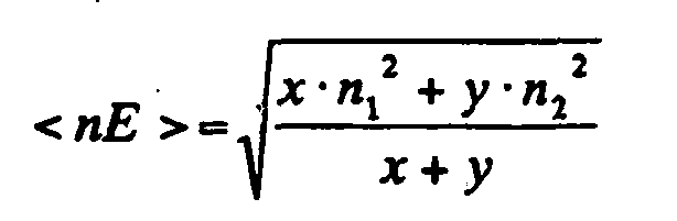
first medium 41, y is a width of theconcavity 43, as indicated inFIG. 9 , n1 is a refraction index of the first medium (substrate), and n2 is a refraction index of the air.
Also, the overall refraction index <nM> with regard to TM (Transvese Magnetic) wave can be expressed by the following expression.
- Further, the
refractor layer 40 may be realized by an array of the modifiedmediums 42 which are distributed to leaveconcavities 43 between the adjacent modifiedmediums 42, as shown inFIG. 10 . In this instance, theconcavities 43 are firstly formed by removing selected portions of the radiation surface by the laser ablation, and subsequently the portions remained between the concavities are modified into the modified medium by the laser modification. The laser utilized is the femto laser having a wavelength of 800 nm and a pulse width of 150 fs (femto-seconds), and is irradiated to the top surface of thesubstrate 10 at a work energy of about 1 µJ/pulse to remove the selected portions by ablation, thereby forming thecylindrical concavities 43 of about 100 nm inside diameter, and is subsequently irradiated to the remaining portions at a work energy of 2 to 15 J/mm2 to form the modifiedmediums 42. -
FIGS. 11 and 12 show a light emitting device in accordance with a second embodiment of the present invention which is identical to the first embodiment except that aphotonic crystal structure 50 is formed inside of thecrystalline substrate 10 as well as the semiconductor layers 21 and 22 for reflecting the light from the interface towards the top radiation surface of the substrate provided with therefractor layer 40. Thephotonic crystal structure 50 includes of a plurality ofpillar crystal units 51 extending vertically in the circumferences of thesubstrate 10 and the semiconductor layers 21 and 22. The pillar crystal units are formed by the laser modification of the substrate, and are arranged at a regular interval of approximately half of the wavelength of the light, presenting a different crystalline structure which is cooperative with the adjacent unmodified substrate for reflecting the light. Thus, the light generated at the interface between the semiconductor layers 21 and 22 are collectively given off through therefractor layer 40 at the top center of thesubstrate 10. Like parts are designated by like reference numerals utilized in the first embodiment -
FIGS. 13 to 16 show a light emitting device in accordance with a third embodiment of the present invention which is identical to the first embodiment except that thecrystalline substrate 10 is formed in its interior with aphotonic crystal structure 50 for reflecting the light towards the radiation surface at the top center face of thesubstrate 10 where therefractor layer 40 is provided. The photonic crystal structure includes a plurality ofspherical crystal units 52 which are arranged along three dimensions in such a pattern as to have different areas in various horizontal sections, as shown inFIGS. 14 to 16 , for reflecting the light towards therefractor layer 40 of reduced area formed in the top center of thesubstrate 10. The spherical crystal units are formed by modifying the substrate with the laser, and are spaced at a regular interval of approximately half of the wavelength of the light. Like parts are designated by like reference numerals. - As shown in
FIG. 17 , the like photonic crystal structure may be formed in the semiconductor layers 21 and 22 to reflect the light towards the top surface of thesubstrate 10, while prohibiting the light from passing sideward out through thefirst semiconductor layer 21 as well as from passing downwardly out through thesecond semiconductor layer 22. Further, as shown inFIG. 18 , thephotonic crystal structure 50 composed of the spherical crystal units may be formed also in the periphery of thesubstrate 10 in order to radiate the light only through therefractor layer 40 at the top surface of the substrate. -
FIGS. 19 and 20 show arefractor layer 40 configured into the Fresnel lens which is applicable to an example disclosed herein. That is, therefractor layer 40 includes an array ofconcavities 43 arranged in a particular pattern to form the Fresnel lens. In detail, therefractor layer 40 has plural sets of theconcavities 43 or concentric grooves about an optical axis M of therefractor layer 40. In each set, the width of the concavity alone is smaller towards the optical axis M, while the added width of the concavity and the adjacent first medium 41 is kept constant. The sets of theconcavities 43 are repeated at a cycle greater than one wavelength of the light generated at the interface of the semiconductor layers, for giving off the light out through therefractor layer 40 towards optical axis M. - As shown in
FIG. 21 , thesecond semiconductor layer 22 may be additionally processed to give a refractor layer 24 of the same structure and function as the refractor layer of thecrystalline substrate 10. The refractor layer 24 is formed in the lower exposed surface of thesecond semiconductor layer 22 around theelectrode 32, for radiating the light effectively also out through thesecond semiconductor layer 22. - When the
second semiconductor layer 22 is not required to give off the light, theelectrode 32 is placed over the entire lower surface of thesemiconductor layer 22 to reflect the back upwards, as shown inFIG. 22 . -
FIG. 23 shows a light emitting device in accordance with a fourth embodiment of the present invention which is identical to the first embodiment except that thecrystalline substrate 10 is shaped to have a plurality of the radiation surfaces each provided with therefractor layer 40. Like parts are designated by like reference numerals. Each radiation surface is a planar surface that forms an angle less than a critical angle (θc) with respect to the light advancing from the center of the interface. Thus, thesubstrate 10 can act to give off the light through all the exposed surfaces, while minimizing the multiple reflections within thesubstrate 10, thereby radiating the light at a maximum efficiency. - The
substrate 10 is processed to give the intended surfaces by being ablated with the laser beams LB, as shown inFIG. 24 , and is subsequently irradiated with the laser beam LB to give the refractor layer in each of the surfaces, as shown inFIG. 25 . It is noted in this connection that therefractor layer 40 may be finished to have anyone of the structures as disclosed herein with reference toFIGS. 3 to 7 . - Alternatively, the
substrate 10 may be shaped into a plan-convex lens having a semispherical radiation surface provided with therefractor layer 40, as shown inFIG. 26 . All points of the semi-spherical radiation surface give an angle less than the critical angle with respect to the light proceeding from the center of the interface between the first and second semiconductor layers 21 and 22. The semi-spherical radiation surface is formed by the laser ablation and is subsequently processed by the laser beam to provide therefractor layer 40. -
FIG. 27 shows a light emitting device in accordance with a further example which is identical to the first embodiment except that thecrystalline substrate 10 is covered with anovercoat 60 made of a material different from the substrate but also transparent to the light emitted from the semiconductor layers. Theovercoat 60 is therefore cooperative with the substrate to define the light guide and has a radiation surface through which the light is given off. Theovercoat 60 is made of the material including quartz glass, epoxy resin, silicon resin, and gallium nitride that is easily processed to give therefractor layer 40 without necessarily resorting to the laser ablation or modification technique as explained hereinbefore. For instance, it is possible to rely on a die impression technique for transcription of an array of concavities into a top surface of theovercoat 60 from adie 70, as shown inFIG. 28 . The top face of the overcoat can be heated by being irradiated with the laser beam in order to facilitate the transcription or the formation of therefractor layer 40 in the top face of theovercoat 60. - Preferably, the
overcoat 60 is selected from the material having the refraction index greater than thesubstrate 10. When, on the other hand, theovercoat 60 is made of the material having a refraction index lower than that of thecrystalline substrate 10, it is preferred to provide anadditional refractor layer 44 at the interface between theovercoat 60 and thesubstrate 10, as shown inFIG. 29 . Theadditional refractor layer 44 is defined by an array of the first medium and the second medium alternating with each other at a regular interval of 1/4 to 4 times the wavelength of the light. For example, the first medium is the material of theovercoat 60, while the second medium is the material of thesubstrate 10. This can be made by forming an array of concavities in the bottom of theovercoat 60 and by pressing the resulting serrated bottom into the top surface of thesubstrate 10. Instead, theadditional refractor layer 44 may have the structure as disclosed with reference toFIGS. 2 and 3 , and is formed on either of the substrate or the overcoat. It is still possible to provide afurther refractor layer 48 at the interface between thesubstrate 10 and thefirst semiconductor layer 21, as illustrated for effectively directing the light towards the top radiation surface of theovercoat 60. -
FIG. 30 shows a modification in which an additionallight guide 80 is superimposed on the lower surface of thesecond semiconductor layer 22 in order to draw the light effectively also through thesemiconductor layer 22 with the addition of therefractor layer 84. Thelight guide 80 is equivalent to theovercoat 60 ofFIG. 29 , and is selected from the material which is different from the semiconductor layer and includes including quartz glass, epoxy resin, and silicon resin. Thelight guide 80 is formed on the entire lower surface of thesecond semiconductor layer 22 other than thesecond electrode 32, and is processed to have therefractor layer 84 of the structure as explained in the above.
Claims (11)
- A method for fabricating a light emitting device, said device comprising:a semiconductor light emitting unit (20) producing a light, said light emitting unit being composed of a first semiconductor layer (21) of a first conductive type and a second semiconductor layer (22) of a second conductive type opposite to said first conductive type, said second semiconductor layer being integrally stacked on said first semiconductor layer to define therebetween an interface;a pair of electrodes (31, 32) being attached respectively to said first and second semiconductor layers to apply a voltage across said interface for emitting the light from around said interface,a light guide (10; 60) superimposed on said first semiconductor layer and directing the light therethrough, said first semiconductor layer being developed directly on said light guide to form a unitary structure with said light guide and said second semiconductor layer;said light guide having a radiation surface through which said light is given off,whereinsaid radiation surface is formed with a refractor layer (40) which comprises an array of a first medium (41) and a second medium (42; 43), said first and second mediums having refraction indexes different from each other and being arranged alternately across said radiation surface,said light guide (10; 60) is made of a transparent crystalline substrate (10) on which said first semiconductor layer (21) is crystallized, and said second semiconductor layer (22) being crystallized on said first semiconductor layer, said first medium is the medium of said transparent crystalline substrate (10),said second medium being a modified medium (42) of said crystalline substrate,characterized in thata laser beam is irradiated on said crystalline substrate (10) to obtain said modified medium (42), which remains in said crystalline substrate (10),wherein said laser beam has a pulse width less than one pico-second.
- The method as set forth in claim 1, wherein a plurality of laser beams are irradiated simultaneously from different directions to form said modified medium (42) by an action of interference between said laser beams.
- A light emitting device obtainable by the method of claim 1.
- The light emitting device as set forth in claim 3, wherein said transparent crystalline substrate (10) includes a photonic crystal structure (50) for reflecting the light from said interface towards said radiation surface.
- The light emitting device as set forth in claim 4, wherein said photonic crystal structure (50) comprises an array of pillar elements extending in a depth direction of said transparent crystalline substrate and being arranged in a regular pattern in which said pillar elements are spaced from each other by a distance corresponding to a wavelength or less of the light from said semiconductor light emitting unit.
- The light emitting device as set forth in claim 3, wherein said semiconductor light emitting unit includes an internal reflector area having a photonic crystal structure (50) for directing the light from said interface towards said light guide.
- The light emitting device a set forth in claim 3, wherein a photonic crystal structure is formed to extend across said transparent crystalline substrate (10) and said semiconductor unit (20) for reflecting the light from said interface towards said radiation surface.
- The light emitting device as set forth in claim 3, wherein said radiation surface comprises a plurality of planar faces each forming an angle less than a critical angle with respect to a light axis of said light proceeding from a center at said interface.
- The light emitting device as set forth in claim 3, wherein said radiation surface is semi-spherical to shape said transparent crystalline substrate into a plan-convex lens, said plan-convex lens having its optical center coincident with a center of said interface.
- The light emitting device as set forth in claim 3, wherein
said transparent crystalline substrate (10) is made of a material selected from a group consisting of sapphire, silicon carbide, gallium nitride, gallium arsenide, and gallium phosphide, and
each of said first and second semiconductor layers (21, 22) being made of a material selected from a group consisting of gallium nitride, gallium arsenide, gallium phosphide, and aluminum nitride. - The light emitting device as set forth in claim 3, wherein each of said first and second mediums is spaced at a regular interval which is from 1/4 to 4 times the wavelength of said light.
Applications Claiming Priority (2)
| Application Number | Priority Date | Filing Date | Title |
|---|---|---|---|
| JP2002220323 | 2002-07-29 | ||
| JP2002220323 | 2002-07-29 |
Publications (3)
| Publication Number | Publication Date |
|---|---|
| EP1387413A2 EP1387413A2 (en) | 2004-02-04 |
| EP1387413A3 EP1387413A3 (en) | 2007-06-13 |
| EP1387413B1 true EP1387413B1 (en) | 2012-08-01 |
Family
ID=30112908
Family Applications (1)
| Application Number | Title | Priority Date | Filing Date |
|---|---|---|---|
| EP03012598A Expired - Lifetime EP1387413B1 (en) | 2002-07-29 | 2003-06-03 | Light emitting diode with enhanced light radiation capability and method for fabricating the same |
Country Status (4)
| Country | Link |
|---|---|
| US (1) | US6878969B2 (en) |
| EP (1) | EP1387413B1 (en) |
| CN (1) | CN1225803C (en) |
| TW (1) | TWI281268B (en) |
Cited By (1)
| Publication number | Priority date | Publication date | Assignee | Title |
|---|---|---|---|---|
| US8513692B2 (en) | 2003-04-15 | 2013-08-20 | Luminus Devices, Inc. | Light emitting devices |
Families Citing this family (101)
| Publication number | Priority date | Publication date | Assignee | Title |
|---|---|---|---|---|
| US7105861B2 (en) * | 2003-04-15 | 2006-09-12 | Luminus Devices, Inc. | Electronic device contact structures |
| US7074631B2 (en) * | 2003-04-15 | 2006-07-11 | Luminus Devices, Inc. | Light emitting device methods |
| US7084434B2 (en) * | 2003-04-15 | 2006-08-01 | Luminus Devices, Inc. | Uniform color phosphor-coated light-emitting diode |
| US7083993B2 (en) * | 2003-04-15 | 2006-08-01 | Luminus Devices, Inc. | Methods of making multi-layer light emitting devices |
| US7098589B2 (en) * | 2003-04-15 | 2006-08-29 | Luminus Devices, Inc. | Light emitting devices with high light collimation |
| US20040259279A1 (en) * | 2003-04-15 | 2004-12-23 | Erchak Alexei A. | Light emitting device methods |
| US7667238B2 (en) * | 2003-04-15 | 2010-02-23 | Luminus Devices, Inc. | Light emitting devices for liquid crystal displays |
| US7274043B2 (en) * | 2003-04-15 | 2007-09-25 | Luminus Devices, Inc. | Light emitting diode systems |
| US7211831B2 (en) * | 2003-04-15 | 2007-05-01 | Luminus Devices, Inc. | Light emitting device with patterned surfaces |
| US7521854B2 (en) * | 2003-04-15 | 2009-04-21 | Luminus Devices, Inc. | Patterned light emitting devices and extraction efficiencies related to the same |
| US7262550B2 (en) * | 2003-04-15 | 2007-08-28 | Luminus Devices, Inc. | Light emitting diode utilizing a physical pattern |
| US7344903B2 (en) * | 2003-09-17 | 2008-03-18 | Luminus Devices, Inc. | Light emitting device processes |
| US7341880B2 (en) * | 2003-09-17 | 2008-03-11 | Luminus Devices, Inc. | Light emitting device processes |
| US7012279B2 (en) * | 2003-10-21 | 2006-03-14 | Lumileds Lighting U.S., Llc | Photonic crystal light emitting device |
| TWI234298B (en) * | 2003-11-18 | 2005-06-11 | Itswell Co Ltd | Semiconductor light emitting diode and method for manufacturing the same |
| US7450311B2 (en) | 2003-12-12 | 2008-11-11 | Luminus Devices, Inc. | Optical display systems and methods |
| JP2005228924A (en) * | 2004-02-13 | 2005-08-25 | Toshiba Corp | Semiconductor light emitting device |
| US7068126B2 (en) * | 2004-03-04 | 2006-06-27 | Discera | Method and apparatus for frequency tuning of a micro-mechanical resonator |
| US20050205883A1 (en) * | 2004-03-19 | 2005-09-22 | Wierer Jonathan J Jr | Photonic crystal light emitting device |
| US6956247B1 (en) * | 2004-05-26 | 2005-10-18 | Lumileds Lighting U.S., Llc | Semiconductor light emitting device including photonic band gap material and luminescent material |
| US7161188B2 (en) * | 2004-06-28 | 2007-01-09 | Matsushita Electric Industrial Co., Ltd. | Semiconductor light emitting element, semiconductor light emitting device, and method for fabricating semiconductor light emitting element |
| US7375380B2 (en) * | 2004-07-12 | 2008-05-20 | Rohm Co., Ltd. | Semiconductor light emitting device |
| US20090023239A1 (en) * | 2004-07-22 | 2009-01-22 | Luminus Devices, Inc. | Light emitting device processes |
| US7442964B2 (en) | 2004-08-04 | 2008-10-28 | Philips Lumileds Lighting Company, Llc | Photonic crystal light emitting device with multiple lattices |
| US20060038188A1 (en) | 2004-08-20 | 2006-02-23 | Erchak Alexei A | Light emitting diode systems |
| US20060043400A1 (en) * | 2004-08-31 | 2006-03-02 | Erchak Alexei A | Polarized light emitting device |
| KR101081146B1 (en) | 2005-01-11 | 2011-11-07 | 엘지이노텍 주식회사 | Semiconductor light emitting diode package of heat conduction type |
| US7394587B2 (en) * | 2005-01-28 | 2008-07-01 | Hewlett-Packard Development Company, L.P. | Apparatus having a photonic crystal |
| US20060204865A1 (en) * | 2005-03-08 | 2006-09-14 | Luminus Devices, Inc. | Patterned light-emitting devices |
| US20070045640A1 (en) * | 2005-08-23 | 2007-03-01 | Erchak Alexei A | Light emitting devices for liquid crystal displays |
| KR100631981B1 (en) * | 2005-04-07 | 2006-10-11 | 삼성전기주식회사 | Vertical group III-nitride light emitting device and method of manufacturing the same |
| KR20080014833A (en) * | 2005-06-09 | 2008-02-14 | 로무 가부시키가이샤 | Semiconductor light emitting device |
| DE102005048408B4 (en) * | 2005-06-10 | 2015-03-19 | Osram Opto Semiconductors Gmbh | Thin-film semiconductor body |
| US8163575B2 (en) | 2005-06-17 | 2012-04-24 | Philips Lumileds Lighting Company Llc | Grown photonic crystals in semiconductor light emitting devices |
| US20070085098A1 (en) * | 2005-10-17 | 2007-04-19 | Luminus Devices, Inc. | Patterned devices and related methods |
| US7348603B2 (en) * | 2005-10-17 | 2008-03-25 | Luminus Devices, Inc. | Anisotropic collimation devices and related methods |
| US7388233B2 (en) * | 2005-10-17 | 2008-06-17 | Luminus Devices, Inc. | Patchwork patterned devices and related methods |
| US7391059B2 (en) * | 2005-10-17 | 2008-06-24 | Luminus Devices, Inc. | Isotropic collimation devices and related methods |
| US20080099777A1 (en) * | 2005-10-19 | 2008-05-01 | Luminus Devices, Inc. | Light-emitting devices and related systems |
| US7349613B2 (en) * | 2006-01-24 | 2008-03-25 | Hewlett-Packard Development Company, L.P. | Photonic crystal devices including gain material and methods for using the same |
| KR101030659B1 (en) * | 2006-03-10 | 2011-04-20 | 파나소닉 전공 주식회사 | Light emitting element |
| KR20070101421A (en) * | 2006-04-10 | 2007-10-17 | 광주과학기술원 | Light emitting diode |
| KR100809227B1 (en) * | 2006-10-27 | 2008-03-05 | 삼성전기주식회사 | Nitride semiconductor light emitting device and manufacturing method |
| US8110838B2 (en) * | 2006-12-08 | 2012-02-07 | Luminus Devices, Inc. | Spatial localization of light-generating portions in LEDs |
| US8110425B2 (en) | 2007-03-20 | 2012-02-07 | Luminus Devices, Inc. | Laser liftoff structure and related methods |
| JP2009044141A (en) * | 2007-07-19 | 2009-02-26 | Eudyna Devices Inc | Optical device, and control method thereof |
| US8368100B2 (en) | 2007-11-14 | 2013-02-05 | Cree, Inc. | Semiconductor light emitting diodes having reflective structures and methods of fabricating same |
| US8575633B2 (en) * | 2008-12-08 | 2013-11-05 | Cree, Inc. | Light emitting diode with improved light extraction |
| US9634191B2 (en) * | 2007-11-14 | 2017-04-25 | Cree, Inc. | Wire bond free wafer level LED |
| US8536584B2 (en) * | 2007-11-14 | 2013-09-17 | Cree, Inc. | High voltage wire bond free LEDS |
| US8378567B2 (en) * | 2007-11-21 | 2013-02-19 | Industrial Technology Research Institute | Light-polarizing structure |
| US7985979B2 (en) | 2007-12-19 | 2011-07-26 | Koninklijke Philips Electronics, N.V. | Semiconductor light emitting device with light extraction structures |
| JP5113573B2 (en) * | 2008-03-24 | 2013-01-09 | パナソニック株式会社 | LED lighting device |
| DE102008030751A1 (en) * | 2008-06-27 | 2009-12-31 | Osram Opto Semiconductors Gmbh | Radiation-emitting semiconductor chip |
| KR101009653B1 (en) * | 2008-10-24 | 2011-01-19 | 주식회사 에피밸리 | Group III nitride semiconductor light emitting device |
| KR101064016B1 (en) * | 2008-11-26 | 2011-09-08 | 엘지이노텍 주식회사 | Light emitting device and manufacturing method |
| KR101040462B1 (en) * | 2008-12-04 | 2011-06-09 | 엘지이노텍 주식회사 | Light emitting device and manufacturing method |
| KR101210172B1 (en) * | 2009-03-02 | 2012-12-07 | 엘지이노텍 주식회사 | Light emitting element |
| KR101075940B1 (en) | 2009-04-13 | 2011-10-21 | 윤무영 | Led chip device structure, method for manufacturing the same, and led chip device obtained by the method |
| KR101125395B1 (en) * | 2009-10-28 | 2012-03-27 | 엘지이노텍 주식회사 | Light emitting device and fabrication method thereof |
| DE102009057780A1 (en) | 2009-12-10 | 2011-06-16 | Osram Opto Semiconductors Gmbh | Optoelectronic semiconductor component and photonic crystal |
| JP5331051B2 (en) * | 2010-04-21 | 2013-10-30 | パナソニック株式会社 | Light emitting element |
| CN101916805A (en) * | 2010-07-13 | 2010-12-15 | 东南大学 | Concentric Photonic Crystal Structures for Increasing the Outer Luminous Efficiency of Light Emitting Diodes |
| US8455882B2 (en) | 2010-10-15 | 2013-06-04 | Cree, Inc. | High efficiency LEDs |
| JP2012099651A (en) * | 2010-11-02 | 2012-05-24 | Toshiba Corp | Light-emitting element |
| US8796053B2 (en) | 2010-12-21 | 2014-08-05 | Ultratech, Inc. | Photolithographic LED fabrication using phase-shift mask |
| JP5117596B2 (en) * | 2011-05-16 | 2013-01-16 | 株式会社東芝 | Semiconductor light emitting device, wafer, and method of manufacturing nitride semiconductor crystal layer |
| US9349918B2 (en) | 2011-07-12 | 2016-05-24 | Marubun Corporation | Light emitting element and method for manufacturing same |
| FR2979034A1 (en) * | 2011-08-12 | 2013-02-15 | St Microelectronics Tours Sas | LIGHT EMITTING DIODE |
| CN103137816B (en) * | 2011-12-03 | 2015-09-30 | 清华大学 | Light-emitting diode |
| CN103137811B (en) * | 2011-12-03 | 2015-11-25 | 清华大学 | Light-emitting diode |
| CN103137812B (en) * | 2011-12-03 | 2015-11-25 | 清华大学 | Light-emitting diode |
| CN103137817B (en) * | 2011-12-03 | 2015-11-25 | 清华大学 | Light-emitting diode |
| CN102431718A (en) * | 2011-12-14 | 2012-05-02 | 吴江市冰心文教用品有限公司 | Pigment packaging skin |
| DE102012003638A1 (en) * | 2012-02-24 | 2013-08-29 | Limo Patentverwaltung Gmbh & Co. Kg | led |
| US10326051B2 (en) | 2012-09-17 | 2019-06-18 | Lumileds Llc | Light emitting device including shaped substrate |
| CN105051593A (en) * | 2013-01-11 | 2015-11-11 | 多点触控有限公司 | Diffusing of direct backlight for a display panel |
| CN108198918B (en) | 2013-05-15 | 2020-10-02 | 皇家飞利浦有限公司 | LEDs with Scattering Features in Substrates |
| US9929311B2 (en) | 2013-07-17 | 2018-03-27 | Marubun Corporation | Semiconductor light emitting element and method for producing the same |
| EP2942818B1 (en) | 2014-03-06 | 2018-01-31 | Marubun Corporation | Deep ultraviolet led and method for manufacturing the same |
| KR102185689B1 (en) * | 2014-06-12 | 2020-12-02 | 엘지이노텍 주식회사 | Light emitting device and light emitting device package including the same |
| CN104393127B (en) * | 2014-11-18 | 2017-05-03 | 中国科学院半导体研究所 | Inversion light emitting diode (LED) and production method thereof |
| USD826871S1 (en) | 2014-12-11 | 2018-08-28 | Cree, Inc. | Light emitting diode device |
| WO2016113935A1 (en) | 2015-01-16 | 2016-07-21 | 丸文株式会社 | Deep ultraviolet led and method for manufacturing same |
| EP3346509B1 (en) | 2015-09-03 | 2021-06-30 | Marubun Corporation | Deep-ultraviolet led and method for manufacturing same |
| US10461221B2 (en) * | 2016-01-18 | 2019-10-29 | Sensor Electronic Technology, Inc. | Semiconductor device with improved light propagation |
| WO2017168811A1 (en) | 2016-03-30 | 2017-10-05 | 丸文株式会社 | Deep ultraviolet led and production method therefor |
| EP3297044A1 (en) * | 2016-09-19 | 2018-03-21 | Nick Shepherd | Improved led emitter, led emitter array and method for manufacturing the same |
| JP7316610B6 (en) | 2018-01-26 | 2024-02-19 | 丸文株式会社 | Deep ultraviolet LED and its manufacturing method |
| CN108417678B (en) * | 2018-03-16 | 2021-06-04 | 厦门市三安光电科技有限公司 | Light-emitting diode structure and fabrication method thereof |
| CN109285928B (en) * | 2018-09-28 | 2020-08-25 | 厦门乾照光电股份有限公司 | Flip LED chip and manufacturing method thereof |
| US11322669B2 (en) * | 2018-12-21 | 2022-05-03 | Lumileds Llc | Color uniformity in converted light emitting diode using nano-structures |
| WO2020128621A2 (en) * | 2018-12-21 | 2020-06-25 | Lumileds Holding B.V. | High brightness directional direct emitter with photonic filter of angular momentum |
| US11041983B2 (en) * | 2018-12-21 | 2021-06-22 | Lumileds Llc | High brightness directional direct emitter with photonic filter of angular momentum |
| US11430919B2 (en) | 2019-04-26 | 2022-08-30 | Lumileds Llc | High brightness LEDs with non-specular nanostructured thin film reflectors |
| CN112968092A (en) * | 2020-11-19 | 2021-06-15 | 重庆康佳光电技术研究院有限公司 | Light emitting device, manufacturing method thereof and display panel with light emitting device |
| US11508888B2 (en) | 2021-02-22 | 2022-11-22 | Lumileds Llc | Light-emitting device assembly with emitter array, micro- or nano-structured lens, and angular filter |
| US11204153B1 (en) | 2021-02-22 | 2021-12-21 | Lumileds Llc | Light-emitting device assembly with emitter array, micro- or nano-structured lens, and angular filter |
| TWI760231B (en) * | 2021-05-24 | 2022-04-01 | 錼創顯示科技股份有限公司 | Micro light-emitting device and display apparatus thereof |
| CN114300603A (en) * | 2021-12-29 | 2022-04-08 | 惠州视维新技术有限公司 | Light emitting device and preparation method thereof, lamp panel, backlight module and display device |
| WO2024129716A1 (en) * | 2022-12-15 | 2024-06-20 | Lumileds Llc | Microleds with nanopatterned surface |
Family Cites Families (9)
| Publication number | Priority date | Publication date | Assignee | Title |
|---|---|---|---|---|
| US5101454A (en) * | 1991-02-20 | 1992-03-31 | At&T Bell Laboratories | Light emitting diode with multifaceted reflector to increase coupling efficiency and alignment tolerance |
| JP2836687B2 (en) | 1993-04-03 | 1998-12-14 | 日亜化学工業株式会社 | Gallium nitride based compound semiconductor light emitting device |
| EP0619608B1 (en) * | 1993-04-07 | 1999-11-03 | Mitsui Chemicals, Inc. | Circuit board for optical devices |
| US5779924A (en) * | 1996-03-22 | 1998-07-14 | Hewlett-Packard Company | Ordered interface texturing for a light emitting device |
| US6784463B2 (en) * | 1997-06-03 | 2004-08-31 | Lumileds Lighting U.S., Llc | III-Phospide and III-Arsenide flip chip light-emitting devices |
| EP0977277A1 (en) * | 1998-07-28 | 2000-02-02 | Interuniversitair Microelektronica Centrum Vzw | Devices for emitting radiation with a high efficiency and a method for fabricating such devices |
| EP2270883A3 (en) * | 1999-12-03 | 2015-09-30 | Cree, Inc. | Enhanced light extraction in LEDs through the use of internal and external optical elements |
| DE10019665A1 (en) * | 2000-04-19 | 2001-10-31 | Osram Opto Semiconductors Gmbh | Luminescent diode chip and method for its production |
| US7023022B2 (en) * | 2000-11-16 | 2006-04-04 | Emcore Corporation | Microelectronic package having improved light extraction |
-
2003
- 2003-05-29 US US10/447,232 patent/US6878969B2/en not_active Expired - Lifetime
- 2003-05-30 TW TW092114672A patent/TWI281268B/en not_active IP Right Cessation
- 2003-06-03 EP EP03012598A patent/EP1387413B1/en not_active Expired - Lifetime
- 2003-06-19 CN CNB031491391A patent/CN1225803C/en not_active Expired - Fee Related
Cited By (1)
| Publication number | Priority date | Publication date | Assignee | Title |
|---|---|---|---|---|
| US8513692B2 (en) | 2003-04-15 | 2013-08-20 | Luminus Devices, Inc. | Light emitting devices |
Also Published As
| Publication number | Publication date |
|---|---|
| TW200402154A (en) | 2004-02-01 |
| EP1387413A2 (en) | 2004-02-04 |
| TWI281268B (en) | 2007-05-11 |
| EP1387413A3 (en) | 2007-06-13 |
| US6878969B2 (en) | 2005-04-12 |
| CN1472826A (en) | 2004-02-04 |
| US20040016936A1 (en) | 2004-01-29 |
| CN1225803C (en) | 2005-11-02 |
Similar Documents
| Publication | Publication Date | Title |
|---|---|---|
| EP1387413B1 (en) | Light emitting diode with enhanced light radiation capability and method for fabricating the same | |
| EP1733438B1 (en) | Laser patterning of light emitting devices and patterned light emitting devices | |
| US7737636B2 (en) | LED assembly with an LED and adjacent lens and method of making same | |
| JP5511114B2 (en) | Micro light-emitting diode array with improved light extraction | |
| US9159882B2 (en) | Semiconductor light-emitting device | |
| KR101601348B1 (en) | Optoelectronic projection apparatus | |
| JP5741996B2 (en) | Light emitting element | |
| KR102153649B1 (en) | A light emitting diode component | |
| US20150014708A1 (en) | Package for light emitting and receiving devices | |
| TW200832755A (en) | Semiconductor and method of manufacturing semiconductor | |
| JP2006054473A (en) | Photonic crystal light emitting device having a plurality of lattices | |
| US7915621B2 (en) | Inverted LED structure with improved light extraction | |
| JP7037070B2 (en) | Manufacturing method of light emitting device | |
| CN117501449A (en) | Patterned reflective grids for LED arrays and displays | |
| EP2943985B1 (en) | Shaped led for enhanced light extraction efficiency | |
| JP7789872B2 (en) | Lighting unit, method for manufacturing a lighting unit, conversion element for an optoelectronic component, radiation source with LED and conversion element, light extraction structure, and optoelectronic device | |
| JP7260828B2 (en) | light emitting device | |
| CN220253262U (en) | Flip LED chip | |
| JP2005197655A (en) | Light emitting device | |
| JP6924642B2 (en) | Semiconductor light emitting element array and semiconductor light emitting device | |
| EP4472681A1 (en) | Micro-leds configured for operation at wavelengths in the far-uvc spectrum | |
| TW202433772A (en) | Laser etching for light-emitting diode devices and related methods | |
| CN118367073A (en) | Light emitting element and method for manufacturing the same | |
| WO1990004853A1 (en) | A print head |
Legal Events
| Date | Code | Title | Description |
|---|---|---|---|
| PUAI | Public reference made under article 153(3) epc to a published international application that has entered the european phase |
Free format text: ORIGINAL CODE: 0009012 |
|
| AK | Designated contracting states |
Kind code of ref document: A2 Designated state(s): AT BE BG CH CY CZ DE DK EE ES FI FR GB GR HU IE IT LI LU MC NL PT RO SE SI SK TR |
|
| AX | Request for extension of the european patent |
Extension state: AL LT LV MK |
|
| PUAL | Search report despatched |
Free format text: ORIGINAL CODE: 0009013 |
|
| AK | Designated contracting states |
Kind code of ref document: A3 Designated state(s): AT BE BG CH CY CZ DE DK EE ES FI FR GB GR HU IE IT LI LU MC NL PT RO SE SI SK TR |
|
| AX | Request for extension of the european patent |
Extension state: AL LT LV MK |
|
| 17P | Request for examination filed |
Effective date: 20071204 |
|
| AKX | Designation fees paid | ||
| RBV | Designated contracting states (corrected) |
Designated state(s): DE IT NL |
|
| RAP1 | Party data changed (applicant data changed or rights of an application transferred) |
Owner name: PANASONIC ELECTRIC WORKS CO., LTD. |
|
| 17Q | First examination report despatched |
Effective date: 20090612 |
|
| REG | Reference to a national code |
Ref country code: DE Ref legal event code: R079 Ref document number: 60341634 Country of ref document: DE Free format text: PREVIOUS MAIN CLASS: H01L0033000000 Ipc: H01L0033200000 |
|
| GRAP | Despatch of communication of intention to grant a patent |
Free format text: ORIGINAL CODE: EPIDOSNIGR1 |
|
| RIC1 | Information provided on ipc code assigned before grant |
Ipc: H01L 33/20 20100101AFI20111215BHEP Ipc: H01L 33/22 20100101ALN20111215BHEP |
|
| RTI1 | Title (correction) |
Free format text: LIGHT EMITTING DIODE WITH ENHANCED LIGHT RADIATION CAPABILITY AND METHOD FOR FABRICATING THE SAME |
|
| RIN1 | Information on inventor provided before grant (corrected) |
Inventor name: TERAUCHI, RYOICHI Inventor name: MATSUSHIMA, TOMOAKI Inventor name: TANAKA, KENICHIRO Inventor name: KUBO, MASAO |
|
| RAP1 | Party data changed (applicant data changed or rights of an application transferred) |
Owner name: PANASONIC CORPORATION |
|
| GRAS | Grant fee paid |
Free format text: ORIGINAL CODE: EPIDOSNIGR3 |
|
| RIN1 | Information on inventor provided before grant (corrected) |
Inventor name: MATSUSHIMA, TOMOAKI Inventor name: KUBO, MASAO Inventor name: TANAKA, KENICHIRO Inventor name: TERAUCHI, RYOICHI |
|
| RIN1 | Information on inventor provided before grant (corrected) |
Inventor name: KUBO, MASAO Inventor name: MATSUSHIMA, TOMOAKI Inventor name: TANAKA, KENICHIRO Inventor name: TERAUCHI, RYOICHI |
|
| GRAA | (expected) grant |
Free format text: ORIGINAL CODE: 0009210 |
|
| AK | Designated contracting states |
Kind code of ref document: B1 Designated state(s): DE IT NL |
|
| REG | Reference to a national code |
Ref country code: DE Ref legal event code: R096 Ref document number: 60341634 Country of ref document: DE Effective date: 20120927 |
|
| REG | Reference to a national code |
Ref country code: NL Ref legal event code: VDEP Effective date: 20120801 |
|
| PG25 | Lapsed in a contracting state [announced via postgrant information from national office to epo] |
Ref country code: NL Free format text: LAPSE BECAUSE OF FAILURE TO SUBMIT A TRANSLATION OF THE DESCRIPTION OR TO PAY THE FEE WITHIN THE PRESCRIBED TIME-LIMIT Effective date: 20120801 |
|
| PG25 | Lapsed in a contracting state [announced via postgrant information from national office to epo] |
Ref country code: IT Free format text: LAPSE BECAUSE OF FAILURE TO SUBMIT A TRANSLATION OF THE DESCRIPTION OR TO PAY THE FEE WITHIN THE PRESCRIBED TIME-LIMIT Effective date: 20120801 |
|
| PLBE | No opposition filed within time limit |
Free format text: ORIGINAL CODE: 0009261 |
|
| STAA | Information on the status of an ep patent application or granted ep patent |
Free format text: STATUS: NO OPPOSITION FILED WITHIN TIME LIMIT |
|
| 26N | No opposition filed |
Effective date: 20130503 |
|
| REG | Reference to a national code |
Ref country code: DE Ref legal event code: R097 Ref document number: 60341634 Country of ref document: DE Effective date: 20130503 |
|
| PGFP | Annual fee paid to national office [announced via postgrant information from national office to epo] |
Ref country code: DE Payment date: 20190619 Year of fee payment: 17 |
|
| REG | Reference to a national code |
Ref country code: DE Ref legal event code: R119 Ref document number: 60341634 Country of ref document: DE |
|
| PG25 | Lapsed in a contracting state [announced via postgrant information from national office to epo] |
Ref country code: DE Free format text: LAPSE BECAUSE OF NON-PAYMENT OF DUE FEES Effective date: 20210101 |