WO2017168811A1 - Deep ultraviolet led and production method therefor - Google Patents
Deep ultraviolet led and production method therefor Download PDFInfo
- Publication number
- WO2017168811A1 WO2017168811A1 PCT/JP2016/082397 JP2016082397W WO2017168811A1 WO 2017168811 A1 WO2017168811 A1 WO 2017168811A1 JP 2016082397 W JP2016082397 W JP 2016082397W WO 2017168811 A1 WO2017168811 A1 WO 2017168811A1
- Authority
- WO
- WIPO (PCT)
- Prior art keywords
- layer
- type algan
- photonic crystal
- periodic structure
- contact layer
- Prior art date
- Legal status (The legal status is an assumption and is not a legal conclusion. Google has not performed a legal analysis and makes no representation as to the accuracy of the status listed.)
- Ceased
Links
Images


Classifications
-
- H—ELECTRICITY
- H10—SEMICONDUCTOR DEVICES; ELECTRIC SOLID-STATE DEVICES NOT OTHERWISE PROVIDED FOR
- H10H—INORGANIC LIGHT-EMITTING SEMICONDUCTOR DEVICES HAVING POTENTIAL BARRIERS
- H10H20/00—Individual inorganic light-emitting semiconductor devices having potential barriers, e.g. light-emitting diodes [LED]
- H10H20/80—Constructional details
- H10H20/81—Bodies
- H10H20/817—Bodies characterised by the crystal structures or orientations, e.g. polycrystalline, amorphous or porous
-
- H—ELECTRICITY
- H10—SEMICONDUCTOR DEVICES; ELECTRIC SOLID-STATE DEVICES NOT OTHERWISE PROVIDED FOR
- H10H—INORGANIC LIGHT-EMITTING SEMICONDUCTOR DEVICES HAVING POTENTIAL BARRIERS
- H10H20/00—Individual inorganic light-emitting semiconductor devices having potential barriers, e.g. light-emitting diodes [LED]
- H10H20/80—Constructional details
- H10H20/81—Bodies
- H10H20/822—Materials of the light-emitting regions
- H10H20/824—Materials of the light-emitting regions comprising only Group III-V materials, e.g. GaP
- H10H20/825—Materials of the light-emitting regions comprising only Group III-V materials, e.g. GaP containing nitrogen, e.g. GaN
-
- H—ELECTRICITY
- H10—SEMICONDUCTOR DEVICES; ELECTRIC SOLID-STATE DEVICES NOT OTHERWISE PROVIDED FOR
- H10H—INORGANIC LIGHT-EMITTING SEMICONDUCTOR DEVICES HAVING POTENTIAL BARRIERS
- H10H20/00—Individual inorganic light-emitting semiconductor devices having potential barriers, e.g. light-emitting diodes [LED]
- H10H20/01—Manufacture or treatment
- H10H20/011—Manufacture or treatment of bodies, e.g. forming semiconductor layers
- H10H20/013—Manufacture or treatment of bodies, e.g. forming semiconductor layers having light-emitting regions comprising only Group III-V materials
- H10H20/0137—Manufacture or treatment of bodies, e.g. forming semiconductor layers having light-emitting regions comprising only Group III-V materials the light-emitting regions comprising nitride materials
-
- H—ELECTRICITY
- H10—SEMICONDUCTOR DEVICES; ELECTRIC SOLID-STATE DEVICES NOT OTHERWISE PROVIDED FOR
- H10H—INORGANIC LIGHT-EMITTING SEMICONDUCTOR DEVICES HAVING POTENTIAL BARRIERS
- H10H20/00—Individual inorganic light-emitting semiconductor devices having potential barriers, e.g. light-emitting diodes [LED]
- H10H20/80—Constructional details
- H10H20/81—Bodies
- H10H20/811—Bodies having quantum effect structures or superlattices, e.g. tunnel junctions
-
- H—ELECTRICITY
- H10—SEMICONDUCTOR DEVICES; ELECTRIC SOLID-STATE DEVICES NOT OTHERWISE PROVIDED FOR
- H10H—INORGANIC LIGHT-EMITTING SEMICONDUCTOR DEVICES HAVING POTENTIAL BARRIERS
- H10H20/00—Individual inorganic light-emitting semiconductor devices having potential barriers, e.g. light-emitting diodes [LED]
- H10H20/80—Constructional details
- H10H20/81—Bodies
- H10H20/814—Bodies having reflecting means, e.g. semiconductor Bragg reflectors
-
- H—ELECTRICITY
- H10—SEMICONDUCTOR DEVICES; ELECTRIC SOLID-STATE DEVICES NOT OTHERWISE PROVIDED FOR
- H10H—INORGANIC LIGHT-EMITTING SEMICONDUCTOR DEVICES HAVING POTENTIAL BARRIERS
- H10H20/00—Individual inorganic light-emitting semiconductor devices having potential barriers, e.g. light-emitting diodes [LED]
- H10H20/80—Constructional details
- H10H20/81—Bodies
- H10H20/815—Bodies having stress relaxation structures, e.g. buffer layers
-
- H—ELECTRICITY
- H10—SEMICONDUCTOR DEVICES; ELECTRIC SOLID-STATE DEVICES NOT OTHERWISE PROVIDED FOR
- H10H—INORGANIC LIGHT-EMITTING SEMICONDUCTOR DEVICES HAVING POTENTIAL BARRIERS
- H10H20/00—Individual inorganic light-emitting semiconductor devices having potential barriers, e.g. light-emitting diodes [LED]
- H10H20/80—Constructional details
- H10H20/81—Bodies
- H10H20/816—Bodies having carrier transport control structures, e.g. highly-doped semiconductor layers or current-blocking structures
-
- H—ELECTRICITY
- H10—SEMICONDUCTOR DEVICES; ELECTRIC SOLID-STATE DEVICES NOT OTHERWISE PROVIDED FOR
- H10H—INORGANIC LIGHT-EMITTING SEMICONDUCTOR DEVICES HAVING POTENTIAL BARRIERS
- H10H20/00—Individual inorganic light-emitting semiconductor devices having potential barriers, e.g. light-emitting diodes [LED]
- H10H20/80—Constructional details
- H10H20/83—Electrodes
- H10H20/832—Electrodes characterised by their material
- H10H20/835—Reflective materials
-
- H—ELECTRICITY
- H10—SEMICONDUCTOR DEVICES; ELECTRIC SOLID-STATE DEVICES NOT OTHERWISE PROVIDED FOR
- H10H—INORGANIC LIGHT-EMITTING SEMICONDUCTOR DEVICES HAVING POTENTIAL BARRIERS
- H10H20/00—Individual inorganic light-emitting semiconductor devices having potential barriers, e.g. light-emitting diodes [LED]
- H10H20/01—Manufacture or treatment
- H10H20/032—Manufacture or treatment of electrodes
-
- H—ELECTRICITY
- H10—SEMICONDUCTOR DEVICES; ELECTRIC SOLID-STATE DEVICES NOT OTHERWISE PROVIDED FOR
- H10H—INORGANIC LIGHT-EMITTING SEMICONDUCTOR DEVICES HAVING POTENTIAL BARRIERS
- H10H20/00—Individual inorganic light-emitting semiconductor devices having potential barriers, e.g. light-emitting diodes [LED]
- H10H20/01—Manufacture or treatment
- H10H20/036—Manufacture or treatment of packages
- H10H20/0363—Manufacture or treatment of packages of optical field-shaping means
Definitions
- the present invention relates to AlGaN-based deep ultraviolet LED technology.
- Deep UV LEDs with an emission wavelength of 280 nm or less are attracting attention as alternative technologies for mercury lamp sterilization lamps in a wide range of application fields such as sterilization, water purification / air purification, and medical care.
- WPE power-light conversion efficiency
- the main reason is that the light extraction efficiency (LEE) is as low as about 6% because emitted light is absorbed by the p-type GaN contact layer by 50% or more.
- a photonic crystal is provided in a thickness direction including an interface between a p-type GaN contact layer and a p-type AlGaN layer, and incident light is reflected to suppress the absorption.
- the depth of the photonic crystal provided in the above literature is about 300 nm, which is equal to or greater than the period.
- the total film thickness of the p-type GaN contact layer and the p-type AlGaN layer is 300 nm or more, or the film thickness of the p-type AlGaN contact layer is 300 nm or more.
- the p-type AlGaN layer has a thickness of 300 nm, it becomes cloudy and sufficient transparency cannot be secured, resulting in a problem that LEE is lowered.
- the object of the present invention is to provide a new technique for increasing the light extraction efficiency in a deep ultraviolet LED.
- a deep ultraviolet LED having a design wavelength ⁇ , a reflective electrode layer, a metal layer, a p-type GaN contact layer, and a p-type AlGaN transparent to the wavelength ⁇ .
- the distance from the end surface of the hole in the substrate direction to the quantum well layer is not less than the total thickness of the barrier layer and the multiple quantum barrier layer (or the electron blocking layer) within 80 nm and the depth thereof h before
- the maximum value of the light extraction efficiency is obtained within the total thickness of the p-type AlGaN layer and the p-type GaN contact layer, and the reflective photonic crystal periodic structure is opened with respect to the TE polarization component.
- the period a of the photonic crystal periodic structure satisfies the Bragg condition for the light of the design wavelength ⁇ , and the order m in the Bragg conditional expression satisfies 1 ⁇ m ⁇ 5
- a deep ultraviolet LED is provided that satisfies R / a where the photonic band gap is maximized when the radius is R and the radius of the hole is R.
- a deep ultraviolet LED having a design wavelength ⁇ , a reflective electrode layer, an ultrathin metal layer, a p-type AlGaN contact layer transparent to the wavelength ⁇ , multiple quantum A p-type AlGaN contact layer having a barrier layer (or electron block layer), a barrier layer, and a quantum well layer in this order from the opposite side of the substrate, the p-type AlGaN contact layer having a thickness of 100 nm or less;
- a reflective photonic crystal periodic structure having a plurality of holes provided in a range in the thickness direction not exceeding the p-type AlGaN contact layer in the substrate direction, the holes in the substrate direction
- the distance from the end face to the quantum well layer is not less than the total thickness of the barrier layer and the multiple quantum barrier layer (or the electron block layer) within 80 nm, and the depth h is the p-type AlGaN contact layer
- the reflective photonic crystal periodic structure has a photonic band gap that is open with respect to the TE
- a deep ultraviolet LED having a design wavelength ⁇ , a reflective electrode layer, a metal layer, a p-type GaN contact layer, and a p-type AlGaN transparent to the wavelength ⁇ .
- it has a reflective photonic crystal periodic structure having a plurality of holes provided at positions not exceeding the reflective electrode layer, and the distance from the end surface in the substrate direction of the holes to the quantum well layer is the barrier.
- a maximum value of the light extraction efficiency is obtained within the range of the total thickness of the multiple quantum barrier layer (or the electron blocking layer) within 80 nm, and the reflective photonic crystal periodic structure is open to the TE polarization component.
- the period a of the periodic structure of the photonic crystal satisfies the Bragg condition for light of the design wavelength ⁇ , and the order m in the Bragg conditional expression is 1 ⁇ m ⁇ 5
- a deep ultraviolet LED characterized by satisfying R / a that maximizes the photonic band gap when R is the radius of the hole.
- a deep ultraviolet LED having a design wavelength ⁇ , a reflective electrode layer, an ultrathin metal layer, a p-type AlGaN contact layer transparent to the wavelength ⁇ , a multiple quantum A barrier layer (or an electron blocking layer), a barrier layer, and a quantum well layer are provided in this order from the side opposite to the substrate, and the thickness of the p-type AlGaN contact layer is within 100 nm, and the p in the substrate direction
- Light having a crystal periodic structure, and the distance from the end surface of the vacancies in the substrate direction to the quantum well layer is 80 nm or more within the total thickness of the barrier layer and the multiple quantum barrier layer (or the electron block layer)
- a deep ultraviolet LED having a design wavelength ⁇ , a reflective electrode layer, a metal layer, a p-type GaN contact layer, and a p-type AlGaN transparent to the wavelength ⁇ .
- the distance from the end surface of the hole in the substrate direction to the quantum well layer is the sum of the thicknesses of the barrier layer and the multiple quantum barrier layer (or the electron blocking layer).
- the maximum value of the light extraction efficiency is obtained when the total value is within 80 nm and the depth h is within the total thickness of the p-type AlGaN layer and the p-type GaN contact layer, and the reflection type photonic crystal period is obtained.
- the structure has a photonic band gap open to the TE polarization component, the period a of the photonic crystal periodic structure satisfies the Bragg condition for the light of the design wavelength ⁇ , and the Bragg conditional expression
- a deep ultraviolet LED characterized in that the order m satisfies 1 ⁇ m ⁇ 5 and R / a that maximizes the photonic band gap when R is the radius of the hole.
- a deep ultraviolet LED having a design wavelength ⁇ , a reflective electrode layer, an ultrathin metal layer, a p-type AlGaN contact layer transparent to the wavelength ⁇ , a multiple quantum A p-type AlGaN contact layer having a barrier layer (or electron block layer), a barrier layer, and a quantum well layer in this order from the opposite side of the substrate, the p-type AlGaN contact layer having a thickness of 100 nm or less;
- a reflective photonic crystal periodic structure having a plurality of holes provided from the thickness direction not exceeding the p-type AlGaN contact layer in the substrate direction to the interface between the p-type AlGaN contact layer and the ultrathin metal layer.
- the distance from the end face of the hole in the substrate direction to the quantum well layer is not less than the total thickness of the barrier layer and the multiple quantum barrier layer (or the electron blocking layer) and not more than 80 nm.
- the maximum value of the light extraction efficiency is obtained when the depth h is within the thickness of the p-type AlGaN contact layer, and the reflective photonic crystal periodic structure is a photonic that is open to the TE polarization component.
- the period a of the photonic crystal periodic structure satisfies the Bragg condition for the light of the design wavelength ⁇ , and the order m in the Bragg conditional expression satisfies 1 ⁇ m ⁇ 5,
- a deep ultraviolet LED characterized by satisfying R / a in which the photonic band gap is maximum when the radius of the hole is R.
- a deep ultraviolet LED having a design wavelength of ⁇ , a reflective electrode layer, a metal layer, a p-type GaN contact layer, and a p-type AlGaN transparent to the wavelength ⁇ A layer, a multiple quantum barrier layer (or electron block layer), a barrier layer, and a quantum well layer in this order from the side opposite to the substrate, and the p-type AlGaN layer has a thickness of 100 nm or less, and the p-type A reflection type photonic crystal period having a plurality of holes provided not exceeding the interface between the GaN contact layer and the p-type AlGaN layer and within the thickness of the p-type GaN contact layer in the substrate direction
- the distance from the end surface of the hole in the substrate direction to the quantum well layer is not less than the total thickness of the barrier layer and the multiple quantum barrier layer (or the electron blocking layer) within 80 nm and the depth thereof h is the p-type G
- the maximum value of the light extraction efficiency can be obtained
- a deep ultraviolet LED manufacturing method which is transparent to a reflective electrode layer, a metal layer, a p-type GaN contact layer, and a wavelength ⁇ .
- a reflective photonic crystal periodic structure having a plurality of holes provided in a range in the thickness direction not exceeding the p-type AlGaN layer in the substrate direction, including an interface with the type AlGaN layer,
- the distance from the end surface in the substrate direction of the hole to the quantum well layer is within 80 nm or more of the total thickness of the barrier layer and the multiple quantum barrier layer (or the electron block layer), and the depth h is the p-type AlGaN layer
- a deep ultraviolet LED manufacturing method wherein the reflective electrode layer, the ultrathin metal layer, and the p-type AlGaN contact layer transparent to the wavelength ⁇ are provided. And a step of preparing a laminated structure containing the p-type AlGaN contact layer within a thickness of 100 nm and in the p-type AlGaN contact layer in the substrate direction.
- a reflective photonic crystal periodic structure having a plurality of holes provided in a range in the thickness direction not exceeding the p-type AlGaN contact layer, from the end surface of the holes in the substrate direction to the quantum well layer
- the distance is not less than the total thickness of the barrier layer and the multiple quantum barrier layer (or the electron blocking layer) within 80 nm and the depth h is within the thickness of the p-type AlGaN contact layer.
- a method of manufacturing a deep ultraviolet LED according to the third aspect which is transparent to a reflective electrode layer, a metal layer, a p-type GaN contact layer, and a wavelength ⁇ .
- the p-type GaN contact layer and the metal layer are penetrated from the thickness direction not exceeding the p-type AlGaN layer in the substrate direction, including the interface with the p-type AlGaN layer, and reach the reflective electrode layer.
- a reflective photonic crystal periodic structure having a plurality of vacancies provided at positions not exceeding the distance between the barrier layer and the multiple quantum barrier layer so that the distance from the end surface in the substrate direction of the vacancies to the quantum well layer (Some A step of preparing a mold for forming a reflective photonic crystal periodic structure capable of obtaining a maximum value of light extraction efficiency within a range of not less than 80 nm and not less than a total thickness of the electron block layer), and on the stacked structure. Forming a resist layer and transferring the mold structure; sequentially etching the laminated structure using the resist layer as a mask to form a photonic crystal periodic structure; and redepositing the reflective electrode layer And a process for producing a deep ultraviolet LED.
- a deep ultraviolet LED manufacturing method comprising a reflective electrode layer, an ultrathin metal layer, and a p-type AlGaN contact that is transparent to a wavelength ⁇ .
- a layered structure containing layers in this order from the opposite side of the substrate, and the p-type AlGaN contact layer has a thickness of 100 nm or less and exceeds the p-type AlGaN contact layer in the substrate direction
- a reflective photonic crystal periodic structure having a plurality of holes provided at positions not penetrating the ultrathin metal layer from the thickness direction and reaching the reflective electrode layer but not exceeding the reflective electrode layer;
- a method for manufacturing a deep ultraviolet LED which includes a step of sequentially etching the laminated structure to form a photonic crystal periodic structure and a step of redepositing a reflective electrode layer.
- a deep ultraviolet LED manufacturing method wherein the reflective electrode layer, the metal layer, the p-type GaN contact layer, and the wavelength ⁇ are transparent.
- a deep ultraviolet LED manufacturing method comprising a reflective electrode layer, an ultrathin metal layer, and a p-type AlGaN contact layer transparent to a wavelength ⁇ . And a step of preparing a laminated structure containing the p-type AlGaN contact layer within a thickness of 100 nm and in the p-type AlGaN contact layer in the substrate direction.
- the distance from the end face in the substrate direction to the quantum well layer is not less than the total thickness of the barrier layer and the multiple quantum barrier layer (or the electron blocking layer) within 80 nm and the depth h is
- a resist layer is formed and the structure of the mold is transferred, and the stacked structure is sequentially etched using the resist layer as a mask to form a photonic crystal periodic structure.
- a deep ultraviolet LED manufacturing method wherein the reflective electrode layer, the metal layer, the p-type GaN contact layer, and the wavelength ⁇ are transparent.
- a step of preparing a laminated structure containing the p-type AlGaN layer in this order from the side opposite to the substrate, the p-type AlGaN layer has a thickness of 100 nm or less, and the p-type GaN contact layer and the p-type AlGaN layer A reflective photonic crystal periodic structure having a plurality of holes provided in the thickness direction of the p-type GaN contact layer in the substrate direction without exceeding the interface with the AlGaN layer,
- the distance from the end surface in the substrate direction of the vacancy to the quantum well layer is not less than 80 nm and not less than the total thickness of the barrier layer and the multiple quantum barrier layer (or the electron block layer), and the depth h is the p-type GaN.
- Contact layer A step of preparing a mold for forming a reflective photonic crystal periodic structure that can obtain a maximum value of light extraction efficiency within a film thickness, and crystal growth to the p-type GaN contact layer in the stacked structure
- a deep ultraviolet process comprising: forming a resist layer and transferring the structure of the mold; and etching the stacked structure sequentially using the resist layer as a mask to form a photonic crystal periodic structure.
- the LEE of deep ultraviolet LEDs can be dramatically improved.
- FIG. 1A (a-1) and 1 (a-2) are a cross-sectional view and a plan view showing an example of the structure of a deep ultraviolet LED using a p-type GaN contact layer photonic crystal according to the first embodiment of the present invention. It is.
- FIG. 1B (b) is a diagram showing a configuration example of a surface-mount package having a deep ultraviolet LED structure using a p-type GaN contact layer photonic crystal according to the first embodiment of the present invention. It is a figure shown as a modification of FIG. 1A. It is a figure shown as a modification of FIG. 1B.
- FIG. 4B (b) is a diagram showing a configuration example of a surface-mount package having a deep ultraviolet LED structure using a p-type AlGaN contact layer photonic crystal according to the second embodiment of the present invention. It is a figure shown as a modification of FIG. 4A. It is a figure shown as a modification of FIG. 4B. It is a figure which shows the FDTD method calculation model at the time of using a photonic crystal for a p-type GaN contact layer. It is a figure which shows the FDTD method calculation model at the time of using a p-type AlGaN contact layer photonic crystal. It is a figure which shows the calculation model and analysis result of a ray tracing method.
- Photonic crystal vicinity electric field distribution It is a figure which shows x component, (a) is Flat, (b) is Ex when a photonic crystal periodic structure is provided, (c) is a photonic crystal periodic structure. It is a figure which shows the calculation result regarding Ex at the time of providing. It is a figure which shows photonic crystal vicinity electric field distribution: y component corresponding to FIG. 8A.
- FIG. 8A It is a figure which shows the photonic crystal vicinity electric field distribution: z component corresponding to FIG. 8A. It is a figure which shows the sum total component of the electric field distribution in the horizontal surface which cross
- FIG. 12A (a-1) and 12 (a-2) are a cross-sectional view and a plan view showing an example of the structure of a deep ultraviolet LED using a p-type GaN contact layer photonic crystal according to the fourth embodiment of the present invention. It is.
- FIG. 12B (b) is a diagram showing a configuration example of a surface-mount package having a deep ultraviolet LED structure using a p-type GaN contact layer photonic crystal according to the fourth embodiment of the present invention. It is a figure which shows the FDTD method calculation model at the time of using a p-type GaN photonic crystal.
- A Enhancement of LEE
- 16A (a-1) and 16 (a-2) are a cross-sectional view and a plan view showing an example of the structure of a deep ultraviolet LED using a p-type GaN contact layer photonic crystal according to the fifth embodiment of the present invention. It is.
- FIG. 16A (a-1) and 16 (a-2) are a cross-sectional view and a plan view showing an example of the structure of a deep ultraviolet LED using a p-type GaN contact layer photonic crystal according to the fifth embodiment of the present invention. It is.
- FIGS. 19A (a-1) and 19 (a-2) are a cross-sectional view and a plan view showing an example of the structure of a deep ultraviolet LED using a p-type AlGaN contact layer photonic crystal according to the sixth embodiment of the present invention. It is.
- FIG. 19A (a-1) and 19 (a-2) are a cross-sectional view and a plan view showing an example of the structure of a deep ultraviolet LED using a p-type AlGaN contact layer photonic crystal according to the sixth embodiment of the present invention. It is.
- 19B (b) is a diagram showing a configuration example of a surface-mount package having a deep ultraviolet LED structure using a p-type AlGaN contact layer photonic crystal according to the sixth embodiment of the present invention. It is a figure which shows the FDTD method calculation model at the time of using a p-type AlGaN photonic crystal.
- 22A (a-1) and 22 (a-2) are a cross-sectional view and a plan view showing an example of the structure of a deep ultraviolet LED using a p-type GaN contact layer photonic crystal according to the seventh embodiment of the present invention. It is.
- FIG. 22B (b) is a diagram showing a configuration example of a surface-mount package having a deep ultraviolet LED structure using a p-type GaN contact layer photonic crystal according to the seventh embodiment of the present invention. It is a figure which shows the FDTD method calculation model at the time of using a p-type GaN photonic crystal.
- FIGS. 1A (a-1) and (a-2). the structure (cross-sectional view and plan view) of an AlGaN-based deep ultraviolet LED having a design wavelength ⁇ of 280 nm is shown in FIGS. 1A (a-1) and (a-2). ).
- FIG. 1B (b) shows a deep ultraviolet LED mounted on a surface mount package.
- the sapphire substrate 1 In order from the top of the cross-sectional view of FIG. 1A (a-1), the sapphire substrate 1, the AlN buffer layer 2, the n-type AlGaN layer 3, the barrier layer 4, the quantum well layer 5, the barrier layer 6, and the multiple layers. It has a quantum barrier layer (MQB) 7, a p-type AlGaN layer (transparent p-type AlGaN layer) 8, a p-type GaN contact layer 9, a Ni layer 10, and an Au reflective electrode layer 11.
- MQB quantum barrier layer
- the p-type AlGaN layer 8 has a film thickness of 100 nm or less, includes the interface between the p-type GaN contact layer 9 and the p-type AlGaN layer 8, and does not exceed the p-type AlGaN layer in the substrate direction.
- the periodic structure 100 is provided, and the photonic crystal periodic structure 100 is provided with a hole (columnar structure, hole) 101 (h) and has a photonic band gap to reflect light with a wavelength ⁇ . It is a photonic crystal periodic structure. Note that it is not preferable to form the photonic crystal periodic structure only in the p-type GaN contact layer 9 because light is absorbed by the p-type GaN contact layer.
- the multiple quantum barrier layer (MQB) 7 may be an electron block layer. The same applies to the following embodiments.
- the reflective photonic crystal periodic structure 100 is formed of a cylinder or the like having a refractive index smaller than that of a p-type AlGaN layer or a p-type GaN contact layer.
- Holes 101 (h) having a cross section of a circle with a radius R have a hole structure formed in a triangular lattice pattern with a period a along the x and y directions. Further, the hole 101 (h) has a structure that does not exceed the interface between the p-type AlGaN layer 8 and the multiple quantum barrier layer 7, and the hole 101 (h) has an end surface in the substrate direction and the quantum well layer 5.
- the distance G is in the range of not less than the sum of the film thicknesses of the barrier layer 6 and the multiple quantum barrier layer 7 and not more than 80 nm. Further, the depth h of the reflective photonic crystal periodic structure 100 is within the total thickness of the p-type AlGaN layer 8 and the p-type GaN contact layer 9.
- the body 101 (h) may have a structure that penetrates the Ni layer 10 and reaches the Au reflective electrode layer 11, but does not reach the interface between the Au reflective electrode layer 11 and air.
- the deep ultraviolet light having the wavelength ⁇ emitted from the quantum well layer 5 is transmitted in the medium while the TE light and the TM light are emitted in all directions and elliptically polarized.
- the photonic crystal periodic structure 100 provided in the vicinity of the quantum well layer 5 is formed with two structures of a p-type AlGaN layer 8 and air having different refractive indexes at the end face, and has a hole radius R and a period a.
- the ratio R / a 0.0.4
- FIG. 2 is obtained when the photonic band structure of TE light is obtained by the plane wave expansion method.
- R / a 0.4 was invented by the inventor himself and described in International Application PCT / JP2015 / 071453 (Prior Art 1), “R / a size, PBG size, light extraction It is a value adopted from the principle that the efficiency increase / decrease rate is proportional to each other.
- the depth does not need to be 300 nm, and even at a shallow depth of about 60 nm.
- the reflection effect more than the structure of the prior art 1 or the like can be obtained.
- the possible range of the order m has also expanded. Note that as m decreases, the period also decreases.
- FIG. 3 is a diagram showing a photonic crystal reflection effect.
- TE light incident from all directions on the photonic crystal periodic structure provided in the vicinity of the quantum well layer completely satisfies the Bragg scattering conditions as indicated by AR1. In order to satisfy the above, it is scattered in this plane and reflected in the direction of the substrate.
- TM light is not Bragg-scattered in the depth direction because there is no PBG, as indicated by a broken line AR2. Therefore, the incident light is not absorbed or lost by the p-type GaN contact layer.
- the layer where the crystal is formed is made thicker by devising the position where the photonic crystal periodic structure is provided in the layer to be provided with the photonic crystal periodic structure.
- a large light extraction efficiency can be obtained by increasing the reflection effect while suppressing white turbidity.
- 4A (a-1) is a cross-sectional view
- FIG. 4A (a-2) is a plan view
- FIG. 4B (b) shows a deep ultraviolet LED mounted on a surface mount package. Specifically, in order from the top of FIG.
- the sapphire substrate 1 the AlN buffer layer 2, the n-type AlGaN layer 3, the barrier layer 4, the quantum well layer 5, the barrier layer 6, and the multiple quantum barrier layer ( MQB) 7, a p-type AlGaN contact layer (transparent p-type AlGaN contact layer) 8a, an ultrathin Ni layer 10a, and an Al reflective electrode layer 11a.
- MQB multiple quantum barrier layer
- the thickness of the p-type AlGaN contact layer 8a is 100 nm or less
- the photonic crystal periodic structure 100 is provided in the p-type AlGaN contact layer 8a within a range not exceeding the p-type AlGaN layer in the substrate direction
- the photonic crystal periodic structure 100 is a reflective photonic crystal periodic structure in which holes (columnar structures, holes) 101 (h) are provided and a photonic band gap is provided to reflect light having a wavelength ⁇ .
- FIG. 4A (a-1), (a-2), and FIG. 4B (b) are shown in FIG. 4C (a-1), (a-2) and FIG. 4D (b).
- the depth of the holes in the photonic crystal periodic structure in the thickness direction penetrates the ultrathin metal layer in the direction opposite to the substrate and reaches the reflective electrode layer, but penetrates the reflective electrode layer.
- the structure is extended to the extent that it is not allowed.
- FIG. 5 shows a photonic crystal calculation model of the p-type GaN contact layer (first embodiment)
- FIG. 6 shows a calculation model of the p-type AlGaN contact layer (second embodiment), respectively.
- FIG. 7A (a-1) is a calculation model of a pGaN contact.
- FIG. 7A (a-2) shows a radiation pattern as an analysis result.
- FIG. 7A (b) shows the details of the model and the light extraction efficiency which is the analysis result.
- FIG. 7A (c-1) is a calculation model of a pAlGaN contact.
- FIG. 7A (c-2) shows a radiation pattern as an analysis result.
- FIG. 7B shows the relationship between the size of the photonic band gap and the reflection / transmission effect, and the light extraction efficiency (LEE) increase / decrease rate in the deep ultraviolet LED, which is obtained by analysis by the FDTD method. It is a figure which shows the detailed processing flow for obtaining the diameter d of this, the period a, and the depth h.
- Step S01 A ratio (R / a) between the period a, which is a periodic structure parameter, and the radius R of the structure is provisionally determined.
- Step S02 The average refractive index n av is calculated from the respective refractive indexes n 1 and n 2 of the previous structure and R / a, and this is substituted into the Bragg condition formula, and the period a and the radius R for each order m are calculated. obtain.
- Step S03 The photonic band structure of TE light is analyzed by a plane wave expansion method using dielectric constants ⁇ 1 and ⁇ 2 of each structure obtained from R / a, wavelength ⁇ , and refractive indexes n 1 and n 2 .
- Step S04 The R / a at which the PBG between the first photonic band and the second photonic band of TE light is maximized is determined by repeated analysis by changing the value of R / a of the provisional determination.
- Step S05 For R / a that maximizes the PBG, the wavelength ⁇ is obtained by simulation analysis using the FDTD method in which the individual period a and the radius R according to the order m of the Bragg condition and the depth h of an arbitrary periodic structure are used as variables. Calculate the light extraction efficiency for.
- Step S06 By repeatedly performing the simulation by the FDTD method, the order m of the Bragg condition that maximizes the light extraction efficiency with respect to the wavelength ⁇ , and the period a, the radius R, and the depth h of the periodic structure parameter corresponding to the order m are determined. To do.
- the analysis was performed by changing the distance from the end face to the quantum well layer from 50 nm to 80 nm and changing the depth of the holes from 40 to 60 nm. The analysis results are shown in Tables 1 and 2.
- Table 2 also shows LEE analysis results when the order m is changed.
- pAlGaN p-type AlGaN contact layer photonic crystal
- pGaN p-type GaN contact layer photonic crystal
- Flat structure without photonic crystal periodic structure
- PhC Depth 40 nm hole depth 40 nm
- Power output value of FDTD method
- FlatLEE% LEE calculation value of ray tracing method
- Enhanced LEE increase / decrease rate of PhC output value with respect to output value of Flat
- PhC LEE% Flat with LEE% of photonic crystal LEE% ⁇ (Enhanced + 100%)
- FIG. 8A shows the electric field distribution Ex component
- FIG. 8A (a) is Flat
- FIG. 8A (b) is a photonic crystal periodic structure (photonic crystal periodic structure is not shown)
- FIG. 8A (c) is a photonic crystal. It is a periodic structure (photonic crystal periodic structure is shown). Each shows the electric field distribution of the cross-sectional structure.
- the photonic crystal periodic structure is removed in FIGS. 8A (c) and 8A (b).
- FIG. 8D (a) is an electric field distribution Etotal of Flat
- FIG. 8D (b) is an electric field distribution Etotal at the center of the photonic crystal.
- the electric field propagates repeatedly in the direction of strength (color shading).
- this analysis result shows that “TE light incident on the photonic crystal periodic structure provided in the vicinity of the quantum well layer from all directions completely satisfies the Bragg scattering condition. In order to satisfy, the physical phenomenon of “scattered in this plane and reflected in the direction of the substrate” is well explained.
- FIG. 9A shows the LEE increase / decrease rate of the p-type AlGaN contact layer
- FIG. 9B shows the LEE increase / decrease rate of the p-type GaN contact layer.
- maximum values are obtained at all depths at a distance of 60 nm from the end face of the hole to the quantum well layer.
- FIG. 9C shows a photonic crystal periodic structure of a p-type GaN contact layer having a distance to the quantum well layer of 60 nm and a hole depth of 60 nm and its flat, as well as a photonic crystal of the p-type AlGaN contact layer.
- the periodic structure and its flat radiation pattern are shown.
- the output value in the front direction (angle 0 to 10 °) with respect to the flat is particularly increased in the photonic crystal periodic structure.
- FIG. 10A shows the light extraction efficiency with a distance to the quantum well layer of 60 nm for the photonic crystals provided in the p-type GaN contact layer and the p-type AlGaN contact layer. From this result, a proportional relationship between the depth (Depth) h of the photonic crystal periodic structure (hole) and LEE is observed.
- the reflection effect of the photonic crystal periodic structure can be obtained by bringing the position of the photonic crystal periodic structure closer to the quantum well structure. It can be seen that the light extraction efficiency is twice as high as that of the structure and slightly more than three times as high as that of the photonic crystal periodic structure of the p-type GaN contact layer.
- FIG. 11 is a diagram illustrating an example of a photonic crystal periodic structure processing process.
- Nanoimprint lithography technology is used for photonic crystal processing. Since the surface of the p-type GaN contact layer 209 has a warp of 100 ⁇ m or more in the convex direction, the mold corresponds to the resin mold 200. Also, a two-layer resist is used in order to keep the hole diameter close to the vertical and accurately in the dry etching.
- a lower layer resist 211 is spin-coated on the surface of the p-type GaN contact layer 209 in a wafer having a deep ultraviolet LED laminated structure laminated up to the p-type GaN contact layer 209.
- a Si-containing upper layer resist 210 is spin-coated to form a two-layer resist (see FIG. 11A).
- the upper resist is pressed with a resin mold 200 having a reversal pattern of a predetermined photonic crystal periodic structure and UV cured to transfer the photonic crystal pattern 212 to the upper resist 210 (see FIG. 11B).
- the upper layer resist 210 is etched with oxygen plasma to form a mask 213. Refer to FIG.
- the distance from the end face of the photonic crystal pattern (hole) 212 to the quantum well layer 205 does not exceed the p-type AlGaN layer 208 by ICP plasma, and the thickness of the barrier layer 206 and the multiple quantum barrier layer 207 is the mask 213.
- Etching is performed to a position not less than the total value and not more than 80 nm, and processed into a shape in which the hole depth is within the total value of the film thicknesses of the p-type AlGaN layer 208 and the p-type GaN contact layer 209. Refer to FIG. Finally, the remaining lower layer resist 211 is cleaned to perform clean surface exposure.
- the metal layer and the reflective electrode layer are formed on the GaN or AlGaN crystal after the photonic crystal pattern is formed, and the structure shown in FIG. 1A, FIG. 4A, FIG. 12A, or FIG. Form.
- the structure shown in FIG. 1C or FIG. 4C is formed by forming a photonic crystal pattern after forming the metal layer and the reflective electrode layer, and re-depositing a reflective electrode layer such as Au or Al thereon.
- a p-type GaN contact layer or a p-type AlGaN contact layer is formed and then a photonic crystal pattern is formed, and a metal layer and a reflective electrode layer are formed thereon by an oblique deposition method, as shown in FIG. 16A or FIG. 19A. Forming a structure.
- the metal layer and the reflective electrode layer are stacked on the surface of the p-type GaN contact layer or the p-type AlGaN contact layer without forming the metal layer and the reflective electrode layer in the hole of the photonic crystal pattern. It is possible.
- 12A (a-1) is a cross-sectional view
- FIG. 12A (a-2) is a plan view
- FIG. 12B (b) shows a deep ultraviolet LED mounted on a surface mount package.
- This LED is the same as the laminated thin film structure of the deep ultraviolet LED in the first embodiment, but the thickness of the p-type GaN contact layer 9 is different from 200 nm. This is to obtain surface flatness by laminating the p-type GaN contact layer thickly in the device manufacturing process.
- the photonic crystal periodic structure 100 is provided in a range including the interface between the p-type GaN contact layer 9 and the p-type AlGaN layer 8 and not exceeding the p-type AlGaN layer in the substrate direction, and the photonic crystal period
- the structure 100 is a reflective photonic crystal periodic structure in which holes (columnar structures, holes) 101 (h) are provided and a photonic band gap is provided to reflect light having a wavelength ⁇ .
- the hole 101 (h) has a structure that does not exceed the interface between the p-type AlGaN layer 8 and the multiple quantum barrier layer 7, and the hole 101 (h) has an end surface in the substrate direction and the quantum well layer 5.
- the distance G is not less than the total thickness of the barrier layer 6 and the multiple quantum barrier layer 7 and within 80 nm.
- the depth h of the reflective photonic crystal periodic structure 100 is within the total thickness of the p-type AlGaN layer 8 and the p-type GaN contact layer 9.
- FIG. 13 shows a photonic crystal calculation model of the p-type GaN contact layer.
- the analysis results are shown in Table 3, FIG. 14 (a) Enhancement of LEE, (b) light extraction efficiency, and (c) radiation pattern (Radiation Pattern).
- FIG. 15A is an electric field intensity distribution in a cross section of a photonic crystal having a depth of 120 nm.
- FIG. 15B is an electric field intensity distribution in a cross section of the photonic crystal having a depth of 140 nm.
- FIG. 15C is an electric field intensity distribution in a cross section of a photonic crystal having a depth of 160 nm.
- 15A to 15C (electric field intensity distribution), it can be seen that light (electric field) that has entered the photonic crystal reaches the deepest part of the photonic crystal at any depth. As the depth increases, light (electric field) penetrates into the p-type GaN contact layer, where light is absorbed and lost.
- the p-type GaN contact layer is thin in order to reduce the depth of the photonic crystal.
- 16A (a-1) is a cross-sectional view
- FIG. 16A (a-2) is a plan view
- FIG. 16B (b) shows a deep ultraviolet LED mounted on a surface mount package.
- the LED is the same as the laminated thin film structure of the deep ultraviolet LED in the fourth embodiment, but the thickness of the p-type GaN contact layer 9 is different from 150 nm. This is a modification from the viewpoint of another method in the device manufacturing process.
- the photonic crystal periodic structure 100 is provided in a range including the interface between the p-type GaN contact layer 9 and the p-type AlGaN layer 8 and not exceeding the p-type AlGaN layer in the substrate direction, and the photonic crystal period
- the structure 100 is a reflective photonic crystal periodic structure in which holes (columnar structures, holes) 101 (h) are provided and a photonic band gap is provided to reflect light having a wavelength ⁇ .
- the void 101 (h) does not exceed the interface between the p-type AlGaN layer 8 and the multiple quantum barrier layer 7, but has a structure that reaches the interface between the p-type GaN contact layer 9 and the Ni layer 10, and
- the distance G between the end surface of the hole 101 (h) in the substrate direction and the quantum well layer 5 is equal to or greater than the total thickness of the barrier layer 6 and the multiple quantum barrier layer 7 and within 80 nm.
- the depth h of the reflective photonic crystal periodic structure 100 is within the total thickness of the p-type AlGaN layer 8 and the p-type GaN contact layer 9.
- FIG. 17 shows a photonic crystal calculation model of the p-type GaN contact layer.
- the analysis results are shown in Table 4, FIG. 18 (a) Enhancement of LEE, FIG. 18 (b) light extraction efficiency, and FIG. 18 (c) radiation pattern (Radiation Pattern).
- 19A (a-1) is a cross-sectional view
- FIG. 19A (a-2) is a plan view
- FIG. 19B (b) shows a deep ultraviolet LED mounted on a surface mount package.
- the LED is the same as the laminated thin film structure of the deep ultraviolet LED in the second embodiment, but is a modification viewed from the viewpoint of another method in the device manufacturing process.
- the p-type AlGaN contact layer 8a has a thickness of 100 nm or less, and the p-type AlGaN contact layer 8a is provided with the photonic crystal periodic structure 100 in a range not exceeding the p-type AlGaN contact layer in the substrate direction.
- the photonic crystal periodic structure 100 is a reflective photonic crystal periodic structure in which holes (columnar structures, holes) 101 (h) are provided and a photonic band gap is provided to reflect light having a wavelength ⁇ .
- the hole 101 (h) does not exceed the interface between the p-type AlGaN contact layer 8a and the multiple quantum barrier layer 7, but has reached the interface between the p-type AlGaN contact layer 8a and the ultrathin Ni layer 10a.
- the distance G between the end surface of the hole 101 (h) in the substrate direction and the quantum well layer 5 is equal to or greater than the total thickness of the barrier layer 6 and the multiple quantum barrier layer 7 and within 80 nm.
- the depth h of the reflective photonic crystal periodic structure 100 is within the thickness of the p-type AlGaN contact layer 8a.
- FIG. 20 shows a photonic crystal calculation model of the p-type AlGaN contact layer.
- the analysis results are shown in Table 5, FIG. 21 (a) Enhancement of LEE, FIG. 21 (b) LEE, and FIG. 21 (c) radiation pattern (Radiation Pattern).
- 22A (a-1) is a cross-sectional view
- FIG. 22A (a-2) is a plan view
- FIG. 22B (b) shows a deep ultraviolet LED mounted on a surface mount package.
- the LED is the same as the laminated thin film structure of the deep ultraviolet LED in the first embodiment and the fourth embodiment, but the position where the photonic crystal periodic structure 100 is provided is different. This is a modification from the viewpoint of another method in the device manufacturing process.
- the photonic crystal periodic structure 100 is provided in the range of the thickness of the p-type GaN contact layer 9 without exceeding the interface between the p-type GaN contact layer 9 and the p-type AlGaN layer 8 in the substrate direction;
- the photonic crystal periodic structure 100 is a reflective photonic crystal periodic structure in which holes (columnar structures, holes) 101 (h) are provided and a photonic band gap is provided to reflect light having a wavelength ⁇ .
- the hole 101 (h) does not exceed the interface between the p-type GaN contact layer 9 and the Ni layer 10, and the distance G from the end surface of the hole 101 (h) in the substrate direction to the quantum well layer 5 is
- the total thickness of the barrier layer 6 and the multiple quantum barrier layer 7 is not less than 80 nm and not less than 80 nm. Further, the depth h of the reflective photonic crystal periodic structure 100 is within the thickness of the p-type GaN contact layer 9.
- the deep ultraviolet light having the wavelength ⁇ emitted from the quantum well layer 5 is transmitted in the medium while being elliptically polarized by emitting TE light and TM light in all directions. Since the photonic crystal periodic structure 100 provided in the vicinity of the quantum well layer 5 is provided within the film thickness of the p-type GaN contact layer 9, two different refractions of the p-type GaN contact layer 9 and air are present at the end face.
- the ratio R / a 0.4, which is the ratio of the radius R of the holes to the period a, is 0.4
- the photonic band structure of TM light is obtained by the plane wave expansion method, and it is confirmed that PBG is obtained between the first photonic band and the second photonic band in TE light.
- FIG. 23 shows a photonic crystal calculation model of the LED structure.
- the thickness of the p-type AlGaN layer 8 is changed in 10 nm steps in the range of 0 nm to 30 nm, and the position of the hole 101 (h) is the end face in the substrate direction with the p-type AlGaN layer 8 and the p-type GaN contact.
- the depth was set to 120 nm from the interface of the layer 9.
- the distance G between the quantum well layer 5 and the end face of the hole 101 (h) in the substrate direction becomes shorter. That is, the distance G is 50 nm when the thickness of the p-type AlGaN layer 8 is 0 nm, and similarly, the distance G is set to be 80 nm when the thickness of the p-type AlGaN layer 8 is 30 nm by changing in 10 nm steps.
- the analysis results are shown in Table 6, FIG. 24 (a) Enhancement of LEE, FIG. 24 (b) light extraction efficiency, and FIG. 24 (c) radiation pattern (Radiation Pattern).
- the light extraction efficiency increase / decrease rate of FIG. 24A increases as the thickness of the p-type AlGaN layer decreases, and the distance G from the quantum well layer 5 is 50 nm (in this case, p-type AlGaN).
- a maximum value of about 2.7 times the strength is obtained when the layer thickness is 0 nm, and about 2.5 times the strength is obtained even when the distance G is 60 nm (also the thickness of the p-type AlGaN layer is 10 nm). It has been.
- the maximum value of 17.3% is obtained by distance G50nm.
- FIG. 24C shows a radiation pattern at a distance G50 nm, and it can be seen that the output in the axial direction (0 to 30 °) increases with respect to Flat.
- an LED device is created.
- the LEE of a deep ultraviolet LED can be dramatically improved by providing a photonic crystal periodic structure in a thin p-type AlGaN layer.
- Each component of the present invention can be arbitrarily selected, and an invention having a selected configuration is also included in the present invention.
- the present invention can be used for deep ultraviolet LEDs.
Landscapes
- Led Devices (AREA)
Abstract
Description
本発明はAlGaN系深紫外LED技術に関する。 The present invention relates to AlGaN-based deep ultraviolet LED technology.
発光波長が280nm以下の深紫外LEDは、殺菌、浄水・空気浄化、医療などの幅広い応用分野で、水銀ランプ殺菌灯の代替技術として注目されている。しかし、LEDの電力光変換効率(WPE)は数%と水銀ランプの20%と比較して著しく低い。その主な理由は、発光した光がp型GaNコンタクト層で50%以上吸収されるために光取出し効率(LEE)が、6%程度と低いことに起因する。 Deep UV LEDs with an emission wavelength of 280 nm or less are attracting attention as alternative technologies for mercury lamp sterilization lamps in a wide range of application fields such as sterilization, water purification / air purification, and medical care. However, the power-light conversion efficiency (WPE) of LEDs is significantly lower than that of several percent and 20% of mercury lamps. The main reason is that the light extraction efficiency (LEE) is as low as about 6% because emitted light is absorbed by the p-type GaN contact layer by 50% or more.
特許文献1によれば、p型GaNコンタクト層とp型AlGaN層との界面を含む厚さ方向にフォトニック結晶を設けて、入射光を反射させて上記吸収を抑制している。
According to
しかしながら、上記文献に設けられたフォトニック結晶の深さは周期と同等以上の300nm程度の深さがないと有効な反射効果が得られない。そのためには、p型GaNコンタクト層とp型AlGaN層の膜厚総和が300nm以上、或いはp型AlGaNコンタクト層の膜厚が300nm以上必要となる。 However, an effective reflection effect cannot be obtained unless the depth of the photonic crystal provided in the above literature is about 300 nm, which is equal to or greater than the period. For this purpose, the total film thickness of the p-type GaN contact layer and the p-type AlGaN layer is 300 nm or more, or the film thickness of the p-type AlGaN contact layer is 300 nm or more.
ところが、p型AlGaN層を膜厚300nmとすると、白濁し、十分な透明度を確保することができず、結果としてLEEが低下するという問題が生じる。 However, if the p-type AlGaN layer has a thickness of 300 nm, it becomes cloudy and sufficient transparency cannot be secured, resulting in a problem that LEE is lowered.
本発明は、深紫外LEDにおいて、光取出し効率を高める新たな技術を提供することを目的とする。 The object of the present invention is to provide a new technique for increasing the light extraction efficiency in a deep ultraviolet LED.
本発明の第一の観点によれば、設計波長をλとする深紫外LEDであって、反射電極層と、金属層と、p型GaNコンタクト層と、波長λに対し透明な、p型AlGaN層、多重量子障壁層(或いは電子ブロック層)、バリア層、量子井戸層とを、基板とは反対側からこの順で有し、前記p型AlGaN層の膜厚が100nm以内で、少なくとも前記p型GaNコンタクト層と前記p型AlGaN層との界面を含み、前記基板方向において前記p型AlGaN層を超えない厚さ方向の範囲内に設けられた複数の空孔を有する反射型フォトニック結晶周期構造を有し、前記空孔の基板方向の端面から量子井戸層までの距離が前記バリア層と前記多重量子障壁層(或いは前記電子ブロック層)の膜厚の合計値以上80nm以内及びその深さhが前記p型AlGaN層と前記p型GaNコンタクト層の膜厚の合計値以内において光取出し効率の極大値が得られ、かつ、前記反射型フォトニック結晶周期構造は、TE偏光成分に対して開かれるフォトニックバンドギャップを有し、前記設計波長λの光に対して前記フォトニック結晶周期構造の周期aがブラッグの条件を満たし、かつ、ブラッグの条件式にある次数mは1≦m≦5を満たし、前記空孔の半径をRとした時、フォトニックバンドギャップが最大となるR/aを満たすことを特徴とする深紫外LEDが提供される。 According to a first aspect of the present invention, a deep ultraviolet LED having a design wavelength λ, a reflective electrode layer, a metal layer, a p-type GaN contact layer, and a p-type AlGaN transparent to the wavelength λ. A layer, a multiple quantum barrier layer (or an electron block layer), a barrier layer, and a quantum well layer in this order from the side opposite to the substrate, and the p-type AlGaN layer has a thickness of 100 nm or less, and at least the p A reflective photonic crystal cycle having a plurality of holes provided in a range in the thickness direction not exceeding the p-type AlGaN layer in the substrate direction, including an interface between the p-type AlGaN layer and the p-type AlGaN layer The distance from the end surface of the hole in the substrate direction to the quantum well layer is not less than the total thickness of the barrier layer and the multiple quantum barrier layer (or the electron blocking layer) within 80 nm and the depth thereof h before The maximum value of the light extraction efficiency is obtained within the total thickness of the p-type AlGaN layer and the p-type GaN contact layer, and the reflective photonic crystal periodic structure is opened with respect to the TE polarization component. It has a photonic band gap, the period a of the photonic crystal periodic structure satisfies the Bragg condition for the light of the design wavelength λ, and the order m in the Bragg conditional expression satisfies 1 ≦ m ≦ 5 A deep ultraviolet LED is provided that satisfies R / a where the photonic band gap is maximized when the radius is R and the radius of the hole is R.
本発明の第二の観点によれば、設計波長をλとする深紫外LEDであって、反射電極層と、極薄膜金属層と、波長λに対し透明な、p型AlGaNコンタクト層、多重量子障壁層(或いは電子ブロック層)、バリア層、量子井戸層とを、基板とは反対側からこの順で有し、前記p型AlGaNコンタクト層の膜厚が100nm以内で、前記p型AlGaNコンタクト層内に、前記基板方向において前記p型AlGaNコンタクト層を超えない厚さ方向の範囲内に設けられた複数の空孔を有する反射型フォトニック結晶周期構造を有し、前記空孔の基板方向の端面から量子井戸層までの距離が前記バリア層と前記多重量子障壁層(或いは前記電子ブロック層)の膜厚の合計値以上80nm以内及びその深さhが前記p型AlGaNコンタクト層の膜厚以内において光取出し効率の極大値が得られ、かつ、前記反射型フォトニック結晶周期構造は、TE偏光成分に対して開かれるフォトニックバンドギャップを有し、前記設計波長λの光に対して前記フォトニック結晶周期構造の周期aがブラッグの条件を満たし、かつ、ブラッグの条件式にある次数mは1≦m≦5を満たし、前記空孔の半径をRとした時、フォトニックバンドギャップが最大となるR/aを満たすことを特徴とする深紫外LEDが提供される。 According to a second aspect of the present invention, a deep ultraviolet LED having a design wavelength λ, a reflective electrode layer, an ultrathin metal layer, a p-type AlGaN contact layer transparent to the wavelength λ, multiple quantum A p-type AlGaN contact layer having a barrier layer (or electron block layer), a barrier layer, and a quantum well layer in this order from the opposite side of the substrate, the p-type AlGaN contact layer having a thickness of 100 nm or less; A reflective photonic crystal periodic structure having a plurality of holes provided in a range in the thickness direction not exceeding the p-type AlGaN contact layer in the substrate direction, the holes in the substrate direction The distance from the end face to the quantum well layer is not less than the total thickness of the barrier layer and the multiple quantum barrier layer (or the electron block layer) within 80 nm, and the depth h is the p-type AlGaN contact layer And the reflective photonic crystal periodic structure has a photonic band gap that is open with respect to the TE polarization component, so that the light of the design wavelength λ can be obtained. On the other hand, when the period a of the periodic structure of the photonic crystal satisfies the Bragg condition, and the order m in the conditional expression of Bragg satisfies 1 ≦ m ≦ 5, and the radius of the hole is R, photonic A deep ultraviolet LED characterized by satisfying R / a that maximizes the band gap is provided.
本発明の第三の観点によれば、設計波長をλとする深紫外LEDであって、反射電極層と、金属層と、p型GaNコンタクト層と、波長λに対し透明な、p型AlGaN層、多重量子障壁層(或いは電子ブロック層)、バリア層、量子井戸層とを、基板とは反対側からこの順で有し、前記p型AlGaN層の膜厚が100nm以内で、少なくとも前記p型GaNコンタクト層と前記p型AlGaN層との界面を含み、前記基板方向において前記p型AlGaN層を超えない厚さ方向からp型GaNコンタクト層及び金属層を貫通し、反射電極層内に達しているが、反射電極層を超えない位置に設けられた複数の空孔を有する反射型フォトニック結晶周期構造を有し、前記空孔の基板方向の端面から量子井戸層までの距離が前記バリア層と前記多重量子障壁層(或いは前記電子ブロック層)の膜厚の合計値以上80nm以内において光取出し効率の極大値が得られ、かつ、前記反射型フォトニック結晶周期構造は、TE偏光成分に対して開かれるフォトニックバンドギャップを有し、前記設計波長λの光に対して前記フォトニック結晶周期構造の周期aがブラッグの条件を満たし、かつ、ブラッグの条件式にある次数mは1≦m≦5を満たし、前記空孔の半径をRとした時、フォトニックバンドギャップが最大となるR/aを満たすことを特徴とする深紫外LEDが提供される。 According to a third aspect of the present invention, a deep ultraviolet LED having a design wavelength λ, a reflective electrode layer, a metal layer, a p-type GaN contact layer, and a p-type AlGaN transparent to the wavelength λ. A layer, a multiple quantum barrier layer (or an electron block layer), a barrier layer, and a quantum well layer in this order from the side opposite to the substrate, and the p-type AlGaN layer has a thickness of 100 nm or less, and at least the p Including the interface between the p-type AlGaN layer and the p-type AlGaN layer, penetrates the p-type GaN contact layer and the metal layer from the thickness direction not exceeding the p-type AlGaN layer in the substrate direction, and reaches the reflective electrode layer However, it has a reflective photonic crystal periodic structure having a plurality of holes provided at positions not exceeding the reflective electrode layer, and the distance from the end surface in the substrate direction of the holes to the quantum well layer is the barrier. Layers and said A maximum value of the light extraction efficiency is obtained within the range of the total thickness of the multiple quantum barrier layer (or the electron blocking layer) within 80 nm, and the reflective photonic crystal periodic structure is open to the TE polarization component. The period a of the periodic structure of the photonic crystal satisfies the Bragg condition for light of the design wavelength λ, and the order m in the Bragg conditional expression is 1 ≦ m ≦ 5 And a deep ultraviolet LED characterized by satisfying R / a that maximizes the photonic band gap when R is the radius of the hole.
本発明の第四の観点によれば、設計波長をλとする深紫外LEDであって、反射電極層と、極薄膜金属層と、波長λに対し透明な、p型AlGaNコンタクト層、多重量子障壁層(或いは電子ブロック層)、バリア層、量子井戸層とを、基板とは反対側からこの順で有し、前記p型AlGaNコンタクト層の膜厚が100nm以内で、前記基板方向において前記p型AlGaNコンタクト層を超えない厚さ方向から極薄膜金属層を貫通し、反射電極層内に達しているが、反射電極層を超えない位置に設けられた複数の空孔を有する反射型フォトニック結晶周期構造を有し、前記空孔の基板方向の端面から量子井戸層までの距離が前記バリア層と前記多重量子障壁層(或いは前記電子ブロック層)の膜厚の合計値以上80nm以内において光取出し効率の極大値が得られ、かつ、前記反射型フォトニック結晶周期構造は、TE偏光成分に対して開かれるフォトニックバンドギャップを有し、前記設計波長λの光に対して前記フォトニック結晶周期構造の周期aがブラッグの条件を満たし、かつ、ブラッグの条件式にある次数mは1≦m≦5を満たし、前記空孔の半径をRとした時、フォトニックバンドギャップが最大となるR/aを満たすことを特徴とする深紫外LEDが提供される。 According to a fourth aspect of the present invention, a deep ultraviolet LED having a design wavelength λ, a reflective electrode layer, an ultrathin metal layer, a p-type AlGaN contact layer transparent to the wavelength λ, a multiple quantum A barrier layer (or an electron blocking layer), a barrier layer, and a quantum well layer are provided in this order from the side opposite to the substrate, and the thickness of the p-type AlGaN contact layer is within 100 nm, and the p in the substrate direction A reflective photonic having a plurality of holes provided at a position not exceeding the reflective electrode layer, though penetrating the ultrathin metal layer from the thickness direction not exceeding the AlGaN contact layer and reaching the reflective electrode layer Light having a crystal periodic structure, and the distance from the end surface of the vacancies in the substrate direction to the quantum well layer is 80 nm or more within the total thickness of the barrier layer and the multiple quantum barrier layer (or the electron block layer) Take The maximum value of the extraction efficiency is obtained, and the reflection type photonic crystal periodic structure has a photonic band gap opened to a TE polarization component, and the photonic crystal with respect to the light of the design wavelength λ When the period a of the periodic structure satisfies the Bragg condition, the order m in the Bragg conditional expression satisfies 1 ≦ m ≦ 5, and the radius of the hole is R, the photonic band gap is maximized. A deep ultraviolet LED characterized by satisfying R / a is provided.
本発明の第五の観点によれば、設計波長をλとする深紫外LEDであって、反射電極層と、金属層と、p型GaNコンタクト層と、波長λに対し透明な、p型AlGaN層、多重量子障壁層(或いは電子ブロック層)、バリア層、量子井戸層とを、基板とは反対側からこの順で有し、前記p型AlGaN層の膜厚が100nm以内で、少なくとも前記p型GaNコンタクト層と前記p型AlGaN層との界面を含み、前記基板方向において前記p型AlGaN層を超えない厚さ方向からp型GaNコンタクト層と金属層の界面にかけて設けられた複数の空孔を有する反射型フォトニック結晶周期構造を有し、前記空孔の基板方向の端面から量子井戸層までの距離が前記バリア層と前記多重量子障壁層(或いは前記電子ブロック層)の膜厚の合計値以上80nm以内及びその深さhが前記p型AlGaN層と前記p型GaNコンタクト層の膜厚の合計値以内において光取出し効率の極大値が得られ、かつ、前記反射型フォトニック結晶周期構造は、TE偏光成分に対して開かれるフォトニックバンドギャップを有し、前記設計波長λの光に対して前記フォトニック結晶周期構造の周期aがブラッグの条件を満たし、かつ、ブラッグの条件式にある次数mは1≦m≦5を満たし、前記空孔の半径をRとした時、フォトニックバンドギャップが最大となるR/aを満たすことを特徴とする深紫外LEDが提供される。 According to a fifth aspect of the present invention, a deep ultraviolet LED having a design wavelength λ, a reflective electrode layer, a metal layer, a p-type GaN contact layer, and a p-type AlGaN transparent to the wavelength λ. A layer, a multiple quantum barrier layer (or an electron block layer), a barrier layer, and a quantum well layer in this order from the side opposite to the substrate, and the p-type AlGaN layer has a thickness of 100 nm or less, and at least the p A plurality of holes provided from the thickness direction not exceeding the p-type AlGaN layer in the substrate direction to the interface between the p-type GaN contact layer and the metal layer, including the interface between the p-type AlGaN layer and the p-type AlGaN layer The distance from the end surface of the hole in the substrate direction to the quantum well layer is the sum of the thicknesses of the barrier layer and the multiple quantum barrier layer (or the electron blocking layer). The maximum value of the light extraction efficiency is obtained when the total value is within 80 nm and the depth h is within the total thickness of the p-type AlGaN layer and the p-type GaN contact layer, and the reflection type photonic crystal period is obtained. The structure has a photonic band gap open to the TE polarization component, the period a of the photonic crystal periodic structure satisfies the Bragg condition for the light of the design wavelength λ, and the Bragg conditional expression There is provided a deep ultraviolet LED characterized in that the order m satisfies 1 ≦ m ≦ 5 and R / a that maximizes the photonic band gap when R is the radius of the hole.
本発明の第六の観点によれば、設計波長をλとする深紫外LEDであって、反射電極層と、極薄膜金属層と、波長λに対し透明な、p型AlGaNコンタクト層、多重量子障壁層(或いは電子ブロック層)、バリア層、量子井戸層とを、基板とは反対側からこの順で有し、前記p型AlGaNコンタクト層の膜厚が100nm以内で、前記p型AlGaNコンタクト層内に、前記基板方向において前記p型AlGaNコンタクト層を超えない厚さ方向からp型AlGaNコンタクト層と極薄膜金属層の界面にかけて設けられた複数の空孔を有する反射型フォトニック結晶周期構造を有し、前記空孔の基板方向の端面から量子井戸層までの距離が前記バリア層と前記多重量子障壁層(或いは前記電子ブロック層)の膜厚の合計値以上80nm以内及びその深さhが前記p型AlGaNコンタクト層の膜厚以内において光取出し効率の極大値が得られ、かつ、前記反射型フォトニック結晶周期構造は、TE偏光成分に対して開かれるフォトニックバンドギャップを有し、前記設計波長λの光に対して前記フォトニック結晶周期構造の周期aがブラッグの条件を満たし、かつ、ブラッグの条件式にある次数mは1≦m≦5を満たし、前記空孔の半径をRとした時、フォトニックバンドギャップが最大となるR/aを満たすことを特徴とする深紫外LEDが提供される。 According to a sixth aspect of the present invention, there is provided a deep ultraviolet LED having a design wavelength λ, a reflective electrode layer, an ultrathin metal layer, a p-type AlGaN contact layer transparent to the wavelength λ, a multiple quantum A p-type AlGaN contact layer having a barrier layer (or electron block layer), a barrier layer, and a quantum well layer in this order from the opposite side of the substrate, the p-type AlGaN contact layer having a thickness of 100 nm or less; A reflective photonic crystal periodic structure having a plurality of holes provided from the thickness direction not exceeding the p-type AlGaN contact layer in the substrate direction to the interface between the p-type AlGaN contact layer and the ultrathin metal layer. And the distance from the end face of the hole in the substrate direction to the quantum well layer is not less than the total thickness of the barrier layer and the multiple quantum barrier layer (or the electron blocking layer) and not more than 80 nm. The maximum value of the light extraction efficiency is obtained when the depth h is within the thickness of the p-type AlGaN contact layer, and the reflective photonic crystal periodic structure is a photonic that is open to the TE polarization component. Having a band gap, the period a of the photonic crystal periodic structure satisfies the Bragg condition for the light of the design wavelength λ, and the order m in the Bragg conditional expression satisfies 1 ≦ m ≦ 5, There is provided a deep ultraviolet LED characterized by satisfying R / a in which the photonic band gap is maximum when the radius of the hole is R.
本発明の第七の観点によれば、設計波長をλとする深紫外LEDであって、反射電極層と、金属層と、p型GaNコンタクト層と、波長λに対し透明な、p型AlGaN層、多重量子障壁層(或いは電子ブロック層)、バリア層、量子井戸層とを、基板とは反対側からこの順で有し、前記p型AlGaN層の膜厚が100nm以内で、前記p型GaNコンタクト層と前記p型AlGaN層との界面を超えず、かつ、前記基板方向において前記p型GaNコンタクト層の膜厚の範囲内に設けられた複数の空孔を有する反射型フォトニック結晶周期構造を有し、前記空孔の基板方向の端面から量子井戸層までの距離が前記バリア層と前記多重量子障壁層(或いは前記電子ブロック層)の膜厚の合計値以上80nm以内及びその深さhが前記p型GaNコンタクト層の膜厚以内において光取出し効率の極大値が得られ、かつ、前記反射型フォトニック結晶周期構造は、TE偏光成分に対して開かれるフォトニックバンドギャップを有し、前記設計波長λの光に対して前記フォトニック結晶周期構造の周期aがブラッグの条件を満たし、かつ、ブラッグの条件式にある次数mは1≦m≦5を満たし、前記空孔の半径をRとした時、フォトニックバンドギャップが最大となるR/aを満たすことを特徴とする深紫外LEDが提供される。 According to a seventh aspect of the present invention, a deep ultraviolet LED having a design wavelength of λ, a reflective electrode layer, a metal layer, a p-type GaN contact layer, and a p-type AlGaN transparent to the wavelength λ A layer, a multiple quantum barrier layer (or electron block layer), a barrier layer, and a quantum well layer in this order from the side opposite to the substrate, and the p-type AlGaN layer has a thickness of 100 nm or less, and the p-type A reflection type photonic crystal period having a plurality of holes provided not exceeding the interface between the GaN contact layer and the p-type AlGaN layer and within the thickness of the p-type GaN contact layer in the substrate direction The distance from the end surface of the hole in the substrate direction to the quantum well layer is not less than the total thickness of the barrier layer and the multiple quantum barrier layer (or the electron blocking layer) within 80 nm and the depth thereof h is the p-type G The maximum value of the light extraction efficiency can be obtained within the thickness of the aN contact layer, and the reflective photonic crystal periodic structure has a photonic band gap that is open with respect to the TE polarization component, and the design wavelength λ When the period a of the periodic structure of the photonic crystal satisfies the Bragg condition and the order m in the conditional expression of Bragg satisfies 1 ≦ m ≦ 5 and the radius of the hole is R A deep ultraviolet LED characterized by satisfying R / a that maximizes the photonic band gap is provided.
本発明の第八の観点によれば、上記第一の観点による深紫外LEDの製造方法であって、反射電極層と、金属層と、p型GaNコンタクト層と、波長λに対し透明な、p型AlGaN層とを、基板とは反対側からこの順で含有する積層構造体を準備する工程と、前記p型AlGaN層の膜厚が100nm以内で、少なくとも前記p型GaNコンタクト層と前記p型AlGaN層との界面を含み、前記基板方向において前記p型AlGaN層を超えない厚さ方向の範囲内に設けられた複数の空孔を有する反射型フォトニック結晶周期構造を有し、前記空孔の基板方向の端面から量子井戸層までの距離が前記バリア層と前記多重量子障壁層(或いは前記電子ブロック層)の膜厚の合計値以上80nm以内及びその深さhが前記p型AlGaN層と前記p型GaNコンタクト層の膜厚の合計値以内において光取出し効率の極大値が得られる反射型フォトニック結晶周期構造を形成するための金型を準備する工程と、前記積層構造体上に、レジスト層を形成し、前記金型の構造を転写する工程と、前記レジスト層をマスクとして順次前記積層構造体をエッチングしてフォトニック結晶周期構造を形成する工程と、を有する深紫外LEDの製造方法が提供される。 According to an eighth aspect of the present invention, there is provided a deep ultraviolet LED manufacturing method according to the first aspect, which is transparent to a reflective electrode layer, a metal layer, a p-type GaN contact layer, and a wavelength λ. a step of preparing a laminated structure containing the p-type AlGaN layer in this order from the side opposite to the substrate; and a thickness of the p-type AlGaN layer within 100 nm, and at least the p-type GaN contact layer and the p-type A reflective photonic crystal periodic structure having a plurality of holes provided in a range in the thickness direction not exceeding the p-type AlGaN layer in the substrate direction, including an interface with the type AlGaN layer, The distance from the end surface in the substrate direction of the hole to the quantum well layer is within 80 nm or more of the total thickness of the barrier layer and the multiple quantum barrier layer (or the electron block layer), and the depth h is the p-type AlGaN layer A step of preparing a mold for forming a reflective photonic crystal periodic structure capable of obtaining a maximum value of light extraction efficiency within a total value of the film thicknesses of the p-type GaN contact layer, and on the stacked structure, Manufacturing a deep ultraviolet LED having a step of forming a resist layer and transferring the structure of the mold, and a step of sequentially etching the laminated structure using the resist layer as a mask to form a photonic crystal periodic structure A method is provided. .
本発明の第九の観点によれば、上記第二の観点による深紫外LEDの製造方法であって、反射電極層と、極薄膜金属層と、波長λに対し透明な、p型AlGaNコンタクト層とを、基板とは反対側からこの順で含有する積層構造体を準備する工程と、前記p型AlGaNコンタクト層の膜厚が100nm以内で、前記p型AlGaNコンタクト層内に、前記基板方向において前記p型AlGaNコンタクト層を超えない厚さ方向の範囲内に設けられた複数の空孔を有する反射型フォトニック結晶周期構造を有し、前記空孔の基板方向の端面から量子井戸層までの距離が前記バリア層と前記多重量子障壁層(或いは前記電子ブロック層)の膜厚の合計値以上80nm以内及びその深さhが前記p型AlGaNコンタクト層の膜厚以内において光取出し効率の極大値が得られる反射型フォトニック結晶周期構造を形成するための金型を準備する工程と、前記積層構造体上に、レジスト層を形成し、前記金型の構造を転写する工程と、前記レジスト層をマスクとして順次前記積層構造体をエッチングしてフォトニック結晶周期構造を形成する工程と、を有する深紫外LEDの製造方法が提供される。 According to a ninth aspect of the present invention, there is provided a deep ultraviolet LED manufacturing method according to the second aspect, wherein the reflective electrode layer, the ultrathin metal layer, and the p-type AlGaN contact layer transparent to the wavelength λ are provided. And a step of preparing a laminated structure containing the p-type AlGaN contact layer within a thickness of 100 nm and in the p-type AlGaN contact layer in the substrate direction. A reflective photonic crystal periodic structure having a plurality of holes provided in a range in the thickness direction not exceeding the p-type AlGaN contact layer, from the end surface of the holes in the substrate direction to the quantum well layer The distance is not less than the total thickness of the barrier layer and the multiple quantum barrier layer (or the electron blocking layer) within 80 nm and the depth h is within the thickness of the p-type AlGaN contact layer. A step of preparing a mold for forming a reflective photonic crystal periodic structure capable of obtaining a maximum value of extraction efficiency, and a step of forming a resist layer on the stacked structure and transferring the structure of the mold And a step of sequentially etching the stacked structure using the resist layer as a mask to form a photonic crystal periodic structure.
本発明の第十の観点によれば、上記第三の観点による深紫外LEDの製造方法であって、反射電極層と、金属層と、p型GaNコンタクト層と、波長λに対し透明な、p型AlGaN層とを、基板とは反対側からこの順で含有する積層構造体を準備する工程と、前記p型AlGaN層の膜厚が100nm以内で、少なくとも前記p型GaNコンタクト層と前記p型AlGaN層との界面を含み、前記基板方向において前記p型AlGaN層を超えない厚さ方向からp型GaNコンタクト層と金属層を貫通し、反射電極層内に達しているが、反射電極層を超えない位置に設けられた複数の空孔を有する反射型フォトニック結晶周期構造を有し、前記空孔の基板方向の端面から量子井戸層までの距離が前記バリア層と前記多重量子障壁層(或いは前記電子ブロック層)の膜厚の合計値以上80nm以内において光取出し効率の極大値が得られる反射型フォトニック結晶周期構造を形成するための金型を準備する工程と、前記積層構造体上に、レジスト層を形成し、前記金型の構造を転写する工程と、前記レジスト層をマスクとして順次前記積層構造体をエッチングしてフォトニック結晶周期構造を形成する工程と、反射電極層を再蒸着させる工程と、を有する深紫外LEDの製造方法が提供される。 According to a tenth aspect of the present invention, there is provided a method of manufacturing a deep ultraviolet LED according to the third aspect, which is transparent to a reflective electrode layer, a metal layer, a p-type GaN contact layer, and a wavelength λ. a step of preparing a laminated structure containing the p-type AlGaN layer in this order from the side opposite to the substrate; and a thickness of the p-type AlGaN layer within 100 nm, and at least the p-type GaN contact layer and the p-type The p-type GaN contact layer and the metal layer are penetrated from the thickness direction not exceeding the p-type AlGaN layer in the substrate direction, including the interface with the p-type AlGaN layer, and reach the reflective electrode layer. A reflective photonic crystal periodic structure having a plurality of vacancies provided at positions not exceeding the distance between the barrier layer and the multiple quantum barrier layer so that the distance from the end surface in the substrate direction of the vacancies to the quantum well layer (Some A step of preparing a mold for forming a reflective photonic crystal periodic structure capable of obtaining a maximum value of light extraction efficiency within a range of not less than 80 nm and not less than a total thickness of the electron block layer), and on the stacked structure. Forming a resist layer and transferring the mold structure; sequentially etching the laminated structure using the resist layer as a mask to form a photonic crystal periodic structure; and redepositing the reflective electrode layer And a process for producing a deep ultraviolet LED.
本発明の第十一の観点によれば、上記第四の観点による深紫外LEDの製造方法であって、反射電極層と、極薄膜金属層と、波長λに対し透明な、p型AlGaNコンタクト層とを、基板とは反対側からこの順で含有する積層構造体を準備する工程と、前記p型AlGaNコンタクト層の膜厚が100nm以内で、前記基板方向において前記p型AlGaNコンタクト層を超えない厚さ方向から極薄膜金属層を貫通し、反射電極層内に達しているが反射電極層を超えない位置に設けられた複数の空孔を有する反射型フォトニック結晶周期構造を有し、前記空孔の基板方向の端面から量子井戸層までの距離が前記バリア層と前記多重量子障壁層(或いは前記電子ブロック層)の膜厚の合計値以上80nm以内において光取出し効率の極大値が得られる反射型フォトニック結晶周期構造を形成するための金型を準備する工程と、前記積層構造体上に、レジスト層を形成し、前記金型の構造を転写する工程と、前記レジスト層をマスクとして順次前記積層構造体をエッチングしてフォトニック結晶周期構造を形成する工程と、反射電極層を再蒸着させる工程と、を有する深紫外LEDの製造方法が提供される。 According to an eleventh aspect of the present invention, there is provided a deep ultraviolet LED manufacturing method according to the fourth aspect, comprising a reflective electrode layer, an ultrathin metal layer, and a p-type AlGaN contact that is transparent to a wavelength λ. A layered structure containing layers in this order from the opposite side of the substrate, and the p-type AlGaN contact layer has a thickness of 100 nm or less and exceeds the p-type AlGaN contact layer in the substrate direction A reflective photonic crystal periodic structure having a plurality of holes provided at positions not penetrating the ultrathin metal layer from the thickness direction and reaching the reflective electrode layer but not exceeding the reflective electrode layer; When the distance from the end surface of the hole in the substrate direction to the quantum well layer is not less than 80 nm and not less than the total thickness of the barrier layer and the multiple quantum barrier layer (or the electron block layer), the light extraction efficiency has a maximum value. A step of preparing a mold for forming a reflective photonic crystal periodic structure to be formed; a step of forming a resist layer on the laminated structure; and transferring the structure of the mold; and masking the resist layer As described above, there is provided a method for manufacturing a deep ultraviolet LED, which includes a step of sequentially etching the laminated structure to form a photonic crystal periodic structure and a step of redepositing a reflective electrode layer.
本発明の第十二の観点によれば、上記第五の観点による深紫外LEDの製造方法であって、反射電極層と、金属層と、p型GaNコンタクト層と、波長λに対し透明な、p型AlGaN層とを、基板とは反対側からこの順で含有する積層構造体を準備する工程と、前記p型AlGaN層の膜厚が100nm以内で、少なくとも前記p型GaNコンタクト層と前記p型AlGaN層との界面を含み、前記基板方向において前記p型AlGaN層を超えない厚さ方向からp型GaNコンタクト層と金属層の界面にかけて設けられた複数の空孔を有する反射型フォトニック結晶周期構造を有し、前記空孔の基板方向の端面から量子井戸層までの距離が前記バリア層と前記多重量子障壁層(或いは前記電子ブロック層)の膜厚の合計値以上80nm以内及びその深さhが前記p型AlGaN層と前記p型GaNコンタクト層の膜厚の合計値以内において光取出し効率の極大値が得られる反射型フォトニック結晶周期構造を形成するための金型を準備する工程と、前記積層構造体のうち前記p型GaNコンタクト層まで結晶成長させた上に、レジスト層を形成し、前記金型の構造を転写する工程と、前記レジスト層をマスクとして順次前記積層構造体をエッチングしてフォトニック結晶周期構造を形成する工程と、前記フォトニック結晶周期構造形成後に金属層と反射電極層をこの順で斜め蒸着させる工程と、を有する深紫外LEDの製造方法が提供される。 According to a twelfth aspect of the present invention, there is provided a deep ultraviolet LED manufacturing method according to the fifth aspect, wherein the reflective electrode layer, the metal layer, the p-type GaN contact layer, and the wavelength λ are transparent. , A step of preparing a laminated structure containing the p-type AlGaN layer in this order from the side opposite to the substrate, and a thickness of the p-type AlGaN layer within 100 nm, and at least the p-type GaN contact layer and the A reflective photonic having a plurality of holes provided from the thickness direction not exceeding the p-type AlGaN layer in the substrate direction to the interface between the p-type GaN contact layer and the metal layer, including the interface with the p-type AlGaN layer It has a crystal periodic structure, and the distance from the end face in the substrate direction of the hole to the quantum well layer is 80 nm or more of the total thickness of the barrier layer and the multiple quantum barrier layer (or the electron block layer) A mold for forming a reflective photonic crystal periodic structure in which the maximum value of the light extraction efficiency is obtained when the depth h is within the total thickness of the p-type AlGaN layer and the p-type GaN contact layer And a step of forming a resist layer on the crystal structure of the stacked structure up to the p-type GaN contact layer and transferring the structure of the mold, and using the resist layer as a mask in sequence. Manufacturing a deep ultraviolet LED comprising: etching the laminated structure to form a photonic crystal periodic structure; and forming the metal layer and the reflective electrode layer obliquely in this order after forming the photonic crystal periodic structure A method is provided.
本発明の第十三の観点によれば上記第六の観点による深紫外LEDの製造方法であって、反射電極層と、極薄膜金属層と、波長λに対し透明な、p型AlGaNコンタクト層とを、基板とは反対側からこの順で含有する積層構造体を準備する工程と、前記p型AlGaNコンタクト層の膜厚が100nm以内で、前記p型AlGaNコンタクト層内に、前記基板方向において前記p型AlGaNコンタクト層を超えない厚さ方向からp型AlGaNコンタクト層と極薄膜金属層の界面にかけて設けられた複数の空孔を有する反射型フォトニック結晶周期構造を有し、前記空孔の基板方向の端面から量子井戸層までの距離が前記バリア層と前記多重量子障壁層(或いは前記電子ブロック層)の膜厚の合計値以上80nm以内及びその深さhが前記p型AlGaNコンタクト層の膜厚以内において光取出し効率の極大値が得られる反射型フォトニック結晶周期構造を形成するための金型を準備する工程と、前記積層構造体のうち前記p型AlGaNコンタクト層まで結晶成長させた上に、レジスト層を形成し、前記金型の構造を転写する工程と、前記レジスト層をマスクとして順次前記積層構造体をエッチングしてフォトニック結晶周期構造を形成する工程と、前記フォトニック結晶周期構造形成後に極薄膜金属層と反射電極層をこの順で斜め蒸着させる工程と、を有する深紫外LEDの製造方法が提供される。 According to a thirteenth aspect of the present invention, there is provided a deep ultraviolet LED manufacturing method according to the sixth aspect, comprising a reflective electrode layer, an ultrathin metal layer, and a p-type AlGaN contact layer transparent to a wavelength λ. And a step of preparing a laminated structure containing the p-type AlGaN contact layer within a thickness of 100 nm and in the p-type AlGaN contact layer in the substrate direction. A reflective photonic crystal periodic structure having a plurality of holes provided from the thickness direction not exceeding the p-type AlGaN contact layer to the interface between the p-type AlGaN contact layer and the ultrathin metal layer, The distance from the end face in the substrate direction to the quantum well layer is not less than the total thickness of the barrier layer and the multiple quantum barrier layer (or the electron blocking layer) within 80 nm and the depth h is A step of preparing a mold for forming a reflective photonic crystal periodic structure capable of obtaining a maximum value of light extraction efficiency within the thickness of the p-type AlGaN contact layer, and the p-type AlGaN of the stacked structure. After growing the crystal up to the contact layer, a resist layer is formed and the structure of the mold is transferred, and the stacked structure is sequentially etched using the resist layer as a mask to form a photonic crystal periodic structure There is provided a method of manufacturing a deep ultraviolet LED having a step and a step of obliquely depositing an ultrathin metal layer and a reflective electrode layer in this order after the photonic crystal periodic structure is formed.
本発明の第十四の観点によれば、上記第七の観点による深紫外LEDの製造方法であって、反射電極層と、金属層と、p型GaNコンタクト層と、波長λに対し透明な、p型AlGaN層とを、基板とは反対側からこの順で含有する積層構造体を準備する工程と、前記p型AlGaN層の膜厚が100nm以内で、前記p型GaNコンタクト層と前記p型AlGaN層との界面を超えず、かつ、前記基板方向において前記p型GaNコンタクト層の膜厚の範囲内に設けられた複数の空孔を有する反射型フォトニック結晶周期構造を有し、前記空孔の基板方向の端面から量子井戸層までの距離が前記バリア層と前記多重量子障壁層(或いは前記電子ブロック層)の膜厚の合計値以上80nm以内及びその深さhが前記p型GaNコンタクト層の膜厚以内において光取出し効率の極大値が得られる反射型フォトニック結晶周期構造を形成するための金型を準備する工程と、前記積層構造体のうち前記p型GaNコンタクト層まで結晶成長させた上に、レジスト層を形成し、前記金型の構造を転写する工程と、前記レジスト層をマスクとして順次前記積層構造体をエッチングしてフォトニック結晶周期構造を形成する工程と、を有する深紫外LEDの製造方法が提供される。 According to a fourteenth aspect of the present invention, there is provided a deep ultraviolet LED manufacturing method according to the seventh aspect, wherein the reflective electrode layer, the metal layer, the p-type GaN contact layer, and the wavelength λ are transparent. , A step of preparing a laminated structure containing the p-type AlGaN layer in this order from the side opposite to the substrate, the p-type AlGaN layer has a thickness of 100 nm or less, and the p-type GaN contact layer and the p-type AlGaN layer A reflective photonic crystal periodic structure having a plurality of holes provided in the thickness direction of the p-type GaN contact layer in the substrate direction without exceeding the interface with the AlGaN layer, The distance from the end surface in the substrate direction of the vacancy to the quantum well layer is not less than 80 nm and not less than the total thickness of the barrier layer and the multiple quantum barrier layer (or the electron block layer), and the depth h is the p-type GaN. Contact layer A step of preparing a mold for forming a reflective photonic crystal periodic structure that can obtain a maximum value of light extraction efficiency within a film thickness, and crystal growth to the p-type GaN contact layer in the stacked structure A deep ultraviolet process comprising: forming a resist layer and transferring the structure of the mold; and etching the stacked structure sequentially using the resist layer as a mask to form a photonic crystal periodic structure. An LED manufacturing method is provided.
本発明によれば、膜厚の薄いp型AlGaN層にフォトニック結晶周期構造を設けることで、深紫外LEDのLEEを飛躍的に向上させることができる。 According to the present invention, by providing a photonic crystal periodic structure in a thin p-type AlGaN layer, the LEE of deep ultraviolet LEDs can be dramatically improved.
以下に、本発明の実施の形態による深紫外LEDについて、図面を参照しながら詳細に説明する。 Hereinafter, a deep ultraviolet LED according to an embodiment of the present invention will be described in detail with reference to the drawings.
(第1の実施の形態)
本発明の第1の実施の形態に係る深紫外LEDとして、設計波長λを280nmとするAlGaN系深紫外LEDの構造(断面図と平面図)を図1A(a-1)、(a-2)に表す。図1B(b)は表面実装型パッケージに搭載した深紫外LEDである。
(First embodiment)
As the deep ultraviolet LED according to the first embodiment of the present invention, the structure (cross-sectional view and plan view) of an AlGaN-based deep ultraviolet LED having a design wavelength λ of 280 nm is shown in FIGS. 1A (a-1) and (a-2). ). FIG. 1B (b) shows a deep ultraviolet LED mounted on a surface mount package.
具体的には、図1A(a-1)の断面図の上から順番に、サファイア基板1、AlNバッファー層2、n型AlGaN層3、バリア層4、量子井戸層5、バリア層6、多重量子障壁層(MQB)7、p型AlGaN層(透明p型AlGaN層)8、p型GaNコンタクト層9、Ni層10、Au反射電極層11を有する。そして、p型AlGaN層8の膜厚が100nm以内であり、p型GaNコンタクト層9とp型AlGaN層8との界面を含み、基板方向においてp型AlGaN層を超えない範囲内にフォトニック結晶周期構造100を設けており、かつ、フォトニック結晶周期構造100は、空孔(柱状構造、ホール)101(h)を設け、フォトニックバンドギャップを有することにより波長λの光を反射する反射型フォトニック結晶周期構造である。尚、フォトニック結晶周期構造をp型GaNコンタクト層9内のみに形成すると、光がp型GaNコンタクト層で吸収されてしまうため、好ましくない。尚、多重量子障壁層(MQB)7は、電子ブロック層であっても良い。以下の実施の形態でも同様である。
Specifically, in order from the top of the cross-sectional view of FIG. 1A (a-1), the
図1A(a-2)にxy平面図として示す通り、反射型フォトニック結晶周期構造100は、円柱などの形状の、p型AlGaN層やp型GaNコンタクト層よりも屈折率が小さい空気などの半径がRの円を断面とする空孔101(h)が、x方向及びy方向に沿って周期aで三角格子状に形成されたホール構造を有する。また、空孔101(h)は、p型AlGaN層8と多重量子障壁層7の界面を超えない構造であり、かつ、空孔101(h)の基板方向の端面と量子井戸層5までの距離Gが、バリア層6と多重量子障壁層7の膜厚の合計値以上80nm以内の範囲にある。さらに、反射型フォトニック結晶周期構造100の深さhが、p型AlGaN層8とp型GaNコンタクト層9の膜厚の合計値以内である。
As shown in the xy plan view of FIG. 1A (a-2), the reflective photonic crystal
尚、デバイス製造プロセス上の別の方法という観点から見た本実施の形態の変形例として、図1C(a-1)、(a-2)、図1D(b)に示すように、柱状構造体101(h)はNi層10を貫通してAu反射電極層11内に達しているがAu反射電極層11と空気の界面には到達していない構造であってもよい。
As a modification of the present embodiment from the viewpoint of another method in the device manufacturing process, as shown in FIGS. 1C (a-1), (a-2), and 1D (b), a columnar structure is used. The body 101 (h) may have a structure that penetrates the
上記の構造においては、量子井戸層5で発光した波長λの深紫外光はTE光とTM光が全方向に放射されて楕円偏光しながら媒質中を伝搬する。量子井戸層5の近傍に設けられたフォトニック結晶周期構造100が、端面において異なる屈折率をもつp型AlGaN層8と空気を二つの構造体として形成され、空孔の半径Rと周期aの比であるR/a=0.4とした時、上記フォトニック結晶の充填率fは次式で計算されf=2π/30.5×(R/a)2=0.58となる。
In the above structure, the deep ultraviolet light having the wavelength λ emitted from the
そして、空気の屈折率n1=1.0、p型AlGaNの屈折率n2=2.583、f=0.58より等価屈折率neffは次式で計算されneff=(n2 2+(n1 2-n2 2)×f)0.5=1.838が得られる。 From the refractive index of air n 1 = 1.0, the refractive index of p-type AlGaN n 2 = 2.583, and f = 0.58, the equivalent refractive index n eff is calculated by the following equation, and n eff = (n 2 2 + (N 1 2 −n 2 2 ) × f) 0.5 = 1.838 is obtained.
そして、発光波長λ=280nmとすると、このフォトニック結晶周期構造がブラッグ散乱条件(mλ/neff=2a、但しneff:等価屈折率、a:周期、m:次数)を満たす場合のTM光、TE光のフォトニックバンド構造を平面波展開法で求めると図2が得られる。 Then, assuming that the emission wavelength λ = 280 nm, this photonic crystal periodic structure satisfies the Bragg scattering condition (mλ / n eff = 2a, where n eff is the equivalent refractive index, a is the period, and m is the order). FIG. 2 is obtained when the photonic band structure of TE light is obtained by the plane wave expansion method.
図2(a)に示すように、TM光ではフォトニックバンドギャップ(PBG)が観測されないが、図2(b)に示すように、TE光では第1フォトニックバンド(ω1TE)と第2フォトニックバンド(ω2TE)間に大きなPBGが観測された。 As shown in FIG. 2A, no photonic band gap (PBG) is observed in TM light, but as shown in FIG. 2B, the first photonic band (ω1TE) and the second photo are emitted in TE light. A large PBG was observed between the nick bands (ω2TE).
尚、R/a=0.4は、発明者自身が発明し、国際出願PCT/JP2015/071453号(先行技術1)に記載した、「R/aの大きさ、PBGの大きさ、光取出し効率増減率が其々比例する」という原理から採用した値である。 R / a = 0.4 was invented by the inventor himself and described in International Application PCT / JP2015 / 071453 (Prior Art 1), “R / a size, PBG size, light extraction It is a value adopted from the principle that the efficiency increase / decrease rate is proportional to each other.
本実施の形態においては、フォトニック結晶の位置が量子井戸層に近づくに従い、周期が先行技術1等における300nmであっても、深さを300nmにする必要がなく、60nm程度の浅い深さでも、先行技術1等の構造以上の反射効果が得られる。また、次数mの取り得る範囲も広がった。尚、mが小さくなると周期も小さくなる。
In the present embodiment, as the position of the photonic crystal approaches the quantum well layer, even if the period is 300 nm in the
図3は、フォトニック結晶反射効果の様子を示す図である。図3(a)、(b)に示すように、量子井戸層の近傍に設けられたフォトニック結晶周期構造にあらゆる方向から入射したTE光は、AR1で示すように、ブラッグ散乱の条件を完全に満たすために、この面内で散乱されて基板の方向に反射される。一方、TM光は破線AR2で示すように、PBGが無いために深さ方向にブラッグ散乱されることはない。従って、入射した光がp型GaNコンタクト層で吸収・消失されない。 FIG. 3 is a diagram showing a photonic crystal reflection effect. As shown in FIGS. 3A and 3B, TE light incident from all directions on the photonic crystal periodic structure provided in the vicinity of the quantum well layer completely satisfies the Bragg scattering conditions as indicated by AR1. In order to satisfy the above, it is scattered in this plane and reflected in the direction of the substrate. On the other hand, TM light is not Bragg-scattered in the depth direction because there is no PBG, as indicated by a broken line AR2. Therefore, the incident light is not absorbed or lost by the p-type GaN contact layer.
従って、本実施の形態による深紫外LEDによれば、フォトニック結晶周期構造を設ける対象となる層において、フォトニック結晶周期構造を設ける位置を工夫することで、結晶を形成する層を厚くすることなく白濁を抑制しつつ、反射効果を増大させることにより、大きな光取り出し効率を得ることができる。 Therefore, according to the deep ultraviolet LED according to the present embodiment, the layer where the crystal is formed is made thicker by devising the position where the photonic crystal periodic structure is provided in the layer to be provided with the photonic crystal periodic structure. A large light extraction efficiency can be obtained by increasing the reflection effect while suppressing white turbidity.
(第2の実施の形態)
次に、本発明の第2の実施の形態に係る深紫外LEDとして、設計波長λを280nmとするAlGaN系深紫外LEDの構造を図4A(a-1)、(a-2)に表す。図4A(a-1)は断面図、図4A(a-2)は平面図である。図4B(b)は表面実装型パッケージに搭載した深紫外LEDである。具体的には、図4A(a-1)の上から順番にサファイア基板1、AlNバッファー層2、n型AlGaN層3、バリア層4、量子井戸層5、バリア層6、多重量子障壁層(MQB)7、p型AlGaNコンタクト層(透明p型AlGaNコンタクト層)8a、極薄膜Ni層10a、Al反射電極層11aを有する。
(Second Embodiment)
Next, as a deep ultraviolet LED according to the second embodiment of the present invention, the structure of an AlGaN-based deep ultraviolet LED having a design wavelength λ of 280 nm is shown in FIGS. 4A (a-1) and (a-2). 4A (a-1) is a cross-sectional view, and FIG. 4A (a-2) is a plan view. FIG. 4B (b) shows a deep ultraviolet LED mounted on a surface mount package. Specifically, in order from the top of FIG. 4A (a-1), the
そしてp型AlGaNコンタクト層8aの膜厚が100nm以内であり、p型AlGaNコンタクト層8aに、基板方向においてp型AlGaN層を超えない範囲内にフォトニック結晶周期構造100を設けており、かつ、フォトニック結晶周期構造100は、空孔(柱状構造体、ホール)101(h)を設け、フォトニックバンドギャップを有することにより波長λの光を反射する反射型フォトニック結晶周期構造である。
The thickness of the p-type
また、図4A(a-1)、(a-2)、図4B(b)の変形例を図4C(a-1)、(a-2)及び図4D(b)に示す。この構造は、フォトニック結晶周期構造の空孔の厚さ方向の深さを、基板とは反対側の方向に、極薄膜金属層を貫通し反射電極層内に達するが、反射電極層を貫通させない範囲まで延長した構造である。 4A (a-1), (a-2), and FIG. 4B (b) are shown in FIG. 4C (a-1), (a-2) and FIG. 4D (b). In this structure, the depth of the holes in the photonic crystal periodic structure in the thickness direction penetrates the ultrathin metal layer in the direction opposite to the substrate and reaches the reflective electrode layer, but penetrates the reflective electrode layer. The structure is extended to the extent that it is not allowed.
その他の、フォトニック結晶周期構造の詳細及び平面波展開法にてフォトニックバンド構造からTE光及びTM光の様子を観測することに関しては、第1の実施の形態と同じである。この場合、フォトニック結晶周期構造に入射した光は面内で散乱されて基板の方向に反射されるために、Al反射電極(反射率90%)に吸収・消失されることはない。
Other details of the periodic structure of the photonic crystal and observation of the state of TE light and TM light from the photonic band structure by the plane wave expansion method are the same as in the first embodiment. In this case, since the light incident on the photonic crystal periodic structure is scattered in the plane and reflected in the direction of the substrate, it is not absorbed or lost by the Al reflective electrode (
そこで、実際に計算モデルを作成してFDTD法で光取出し効率増減率とフォトニック結晶近傍の電界分布(Ex、Ey、Ez)成分を解析してフォトニック結晶周期構造の反射効果を検証した。 Therefore, a calculation model was actually created and the light extraction efficiency change rate and the electric field distribution (Ex, Ey, Ez) component in the vicinity of the photonic crystal were analyzed by the FDTD method to verify the reflection effect of the photonic crystal periodic structure.
図5にp型GaNコンタクト層のフォトニック結晶計算モデル(第1の実施の形態)、図6にp型AlGaNコンタクト層の計算モデル(第2の実施の形態)を其々示す。 5 shows a photonic crystal calculation model of the p-type GaN contact layer (first embodiment), and FIG. 6 shows a calculation model of the p-type AlGaN contact layer (second embodiment), respectively.
また、光取出し効率(LEE)を求めるために、計算モデルを作成して光線追跡法で解析した(図7A参照)。図7A(a-1)はpGaNコンタクトの計算モデルである。図7A(a-2)は解析結果で放射パターンである。図7A(b)にモデルの詳細と解析結果である光取出し効率を示した。図7A(c-1)は、pAlGaNコンタクトの計算モデルである。図7A(c-2)は解析結果で放射パターンである。 Also, in order to obtain the light extraction efficiency (LEE), a calculation model was created and analyzed by the ray tracing method (see FIG. 7A). FIG. 7A (a-1) is a calculation model of a pGaN contact. FIG. 7A (a-2) shows a radiation pattern as an analysis result. FIG. 7A (b) shows the details of the model and the light extraction efficiency which is the analysis result. FIG. 7A (c-1) is a calculation model of a pAlGaN contact. FIG. 7A (c-2) shows a radiation pattern as an analysis result.
図7Bは、フォトニックバンドギャップの大きさと反射・透過効果の関係、並びに、深紫外LEDにおける光取出し効率(LEE)増減率をFDTD法による解析で求め、LEE増減率が最大となるフォトニック結晶の直径d、周期a及び深さhを得るための詳細な処理フローを示す図である。
(ステップS01)
周期構造パラメータである周期aと構造体の半径Rの比(R/a)を仮決定する。
(ステップS02)
前期構造体のそれぞれの屈折率n1とn2、及びこれらとR/aから平均屈折率navを算出し、これをブラッグ条件の式に代入し、次数mごとの周期aと半径Rを得る。
(ステップS03)
R/a及び波長λ並びに前記屈折率n1、n2から得られる各構造体の誘電率ε1及びε2を用いた平面波展開法により、TE光のフォトニックバンド構造を解析する。
(ステップS04)
TE光の第一フォトニックバンドと第二フォトニックバンド間のPBGが最大となるR/aを、前記仮決定のR/aの値を変えて繰り返し行う解析により決定する。
(ステップS05)
PBGを最大にするR/aについて、ブラッグ条件の次数mに応じた個別の周期a及び半径R、並びに、任意の周期構造の深さhを変数として行うFDTD法によるシミュレーション解析により、前記波長λに対する光取出し効率を求める。
(ステップS06)
FDTD法によるシミュレーションを繰り返し行うことにより、波長λに対する光取出し効率が最大となるブラッグ条件の次数mと、その次数mに対応する周期構造パラメータの周期a、半径R、及び、深さhを決定する。
FIG. 7B shows the relationship between the size of the photonic band gap and the reflection / transmission effect, and the light extraction efficiency (LEE) increase / decrease rate in the deep ultraviolet LED, which is obtained by analysis by the FDTD method. It is a figure which shows the detailed processing flow for obtaining the diameter d of this, the period a, and the depth h.
(Step S01)
A ratio (R / a) between the period a, which is a periodic structure parameter, and the radius R of the structure is provisionally determined.
(Step S02)
The average refractive index n av is calculated from the respective refractive indexes n 1 and n 2 of the previous structure and R / a, and this is substituted into the Bragg condition formula, and the period a and the radius R for each order m are calculated. obtain.
(Step S03)
The photonic band structure of TE light is analyzed by a plane wave expansion method using dielectric constants ε 1 and ε 2 of each structure obtained from R / a, wavelength λ, and refractive indexes n 1 and n 2 .
(Step S04)
The R / a at which the PBG between the first photonic band and the second photonic band of TE light is maximized is determined by repeated analysis by changing the value of R / a of the provisional determination.
(Step S05)
For R / a that maximizes the PBG, the wavelength λ is obtained by simulation analysis using the FDTD method in which the individual period a and the radius R according to the order m of the Bragg condition and the depth h of an arbitrary periodic structure are used as variables. Calculate the light extraction efficiency for.
(Step S06)
By repeatedly performing the simulation by the FDTD method, the order m of the Bragg condition that maximizes the light extraction efficiency with respect to the wavelength λ, and the period a, the radius R, and the depth h of the periodic structure parameter corresponding to the order m are determined. To do.
上記のような発明者の知見に基づいて、先ず、ブラッグ散乱条件の次数m=4、R/a=0.4における空孔の直径、周期を求め、フォトニック結晶周期構造中の空孔の端面から量子井戸層までの距離を50nm~80nm及び空孔の深さを40~60nm間で変化させて解析した。解析結果を表1、表2に記載する。


表1に示すように、pAlGaN単層の場合、pGaN単層の場合及びpGaN/pAlGaN2層の場合におけるLEEの解析結果が示されている。 As shown in Table 1, LEE analysis results in the case of a pAlGaN single layer, a pGaN single layer, and a pGaN / pAlGaN two layer are shown.
また、表2には、次数mを変化させた場合にけるLEEの解析結果が示されている。 Table 2 also shows LEE analysis results when the order m is changed.
尚、以下の説明において、pAlGaN:p型AlGaNコンタクト層のフォトニック結晶、pGaN:p型GaNコンタクト層のフォトニック結晶、Flat:フォトニック結晶周期構造の無い構造、PhC Depth 40nm:空孔の深さが40nm、Power:FDTD法の出力値、FlatLEE%:光線追跡法のLEE計算値、Enhanced:Flatの出力値に対するPhC出力値のLEE増減率、PhC LEE%:フォトニック結晶のLEE%でFlat LEE%×(Enhanced+100%)、m4:次数m=4、G50nm:空孔の端面から量子井戸層までの距離が50nm、Diameter:空孔の直径、Period:フォトニック結晶の周期、と定義する。
In the following description, pAlGaN: p-type AlGaN contact layer photonic crystal, pGaN: p-type GaN contact layer photonic crystal, Flat: structure without photonic crystal periodic structure,
フォトニック結晶周期構造の反射効果の実証として、特にp型GaNコンタクト層のフォトニック結晶で最も増減率の高かったm=3(直径:183nm、周期:228nm、深さ:60nm)のフォトニック結晶近傍の電界分布を観測した。図8Aは、電界分布Ex成分で、図8A(a)がFlat,図8A(b)がフォトニック結晶周期構造(フォトニック結晶周期構造を図示せず)、図8A(c)がフォトニック結晶周期構造(フォトニック結晶周期構造を図示)である。それぞれは、断面構造の電界分布を示している。但し、わかりやすいように、図8A(c)、図8A(b)では、フォトニック結晶周期構造を取り除いている。 As a demonstration of the reflection effect of the photonic crystal periodic structure, the photonic crystal of m = 3 (diameter: 183 nm, period: 228 nm, depth: 60 nm), which has the highest rate of increase / decrease, especially in the p-type GaN contact layer photonic crystal The electric field distribution in the vicinity was observed. 8A shows the electric field distribution Ex component, FIG. 8A (a) is Flat, FIG. 8A (b) is a photonic crystal periodic structure (photonic crystal periodic structure is not shown), and FIG. 8A (c) is a photonic crystal. It is a periodic structure (photonic crystal periodic structure is shown). Each shows the electric field distribution of the cross-sectional structure. However, for easy understanding, the photonic crystal periodic structure is removed in FIGS. 8A (c) and 8A (b).
尚、それぞれの図面の右側には、実験結果がわかりやすいように簡単な電界の凡例を示した。また、各層の境界を示すとともに各層の名称を付記した。 In addition, on the right side of each drawing, a simple electric field legend is shown so that the experimental results can be easily understood. Moreover, the boundary of each layer was shown and the name of each layer was added.
Flatではp型GaNコンタクト層とNi層との部分に強度の高い電界成分Exが観測されるのに対して(図8A(a))、フォトニック結晶周期構造を設けた構造ではp型GaNコンタクト層とNi層との部分(図8A(b)のA1、図8A(c)の図のA2領域参照)に強度の高い電界成分Exは観測されていない。 In Flat, a strong electric field component Ex is observed between the p-type GaN contact layer and the Ni layer (FIG. 8A (a)), whereas in the structure provided with the photonic crystal periodic structure, the p-type GaN contact is provided. A high-intensity electric field component Ex is not observed in the portion between the layer and the Ni layer (see A1 in FIG. 8A (b) and A2 region in FIG. 8A (c)).
この結果は、フォトニック結晶周期構造を設けた構造では、p型GaNコンタクト層とNi層との部分におけるフォトニック結晶による反射効果が得られていることを実証している。図8Bの電界分布のEy成分及び図8Cの電界分布のEz成分においても、図8AのEx成分と同様の現象が観測された(A3、A4の領域参照)。 This result demonstrates that the reflection effect by the photonic crystal is obtained in the p-type GaN contact layer and the Ni layer in the structure provided with the photonic crystal periodic structure. In the Ey component of the electric field distribution of FIG. 8B and the Ez component of the electric field distribution of FIG. 8C, the same phenomenon as that of the Ex component of FIG. 8A was observed (refer to areas A3 and A4).
更に、電界分布Ex、Ey、Ezの合計成分であるEtotalについて、フォトニック結晶空孔の深さ方向の中間点でこの空孔に対して垂直に交差する水平面の電界分布を観測した(図8D参照)。 Further, for Etotal, which is the total component of the electric field distributions Ex, Ey, Ez, the electric field distribution on the horizontal plane perpendicular to the vacancies was observed at the intermediate point in the depth direction of the photonic crystal vacancies (FIG. 8D). reference).
図8D(a)がFlatの電界分布Etotalで、図8D(b)がフォトニック結晶中心部の電界分布Etotalである。図8D(a)のFlatにおいては、電界が外側に向かって強弱(色の濃淡)を繰り返して伝搬している。 FIG. 8D (a) is an electric field distribution Etotal of Flat, and FIG. 8D (b) is an electric field distribution Etotal at the center of the photonic crystal. In the flat in FIG. 8D (a), the electric field propagates repeatedly in the direction of strength (color shading).
それに対して、図8D(b)のフォトニック結晶を設けた構造においては、各空孔間に電界が滞留して、特に中心部分で色濃く(図中においては白く表示)表示されている。これはこの部分でブラッグ散乱が誘発されて定在波を形成している様子を示している。そして、その直後に、基板の方向に光が反射されていく。 On the other hand, in the structure provided with the photonic crystal of FIG. 8D (b), an electric field stays between the vacancies and is displayed in a particularly dark color (indicated in white in the figure) at the center. This shows that Bragg scattering is induced in this part to form a standing wave. Immediately thereafter, light is reflected in the direction of the substrate.
従って、この解析結果は、図3を参照して説明したように、『量子井戸層の近傍に設けられたフォトニック結晶周期構造にあらゆる方向から入射したTE光は、ブラッグ散乱の条件を完全に満たすために、この面内で散乱されて基板の方向に反射される』という物理現象を良く説明している。 Therefore, as described with reference to FIG. 3, this analysis result shows that “TE light incident on the photonic crystal periodic structure provided in the vicinity of the quantum well layer from all directions completely satisfies the Bragg scattering condition. In order to satisfy, the physical phenomenon of “scattered in this plane and reflected in the direction of the substrate” is well explained.
FDTD法によるLEE増減率の解析結果を図9に示す。 The analysis result of the LEE increase / decrease rate by the FDTD method is shown in FIG.
図9(a)がp型AlGaNコンタクト層、図9(b)がp型GaNコンタクト層のフォトニック結晶のLEE増減率である。特徴的な現象として、空孔の端面から量子井戸層までの距離60nmでは、全ての深さにおいて極大値が得られていることである。また、図9(c)に量子井戸層までの距離60nm、空孔の深さ60nmからなるp型GaNコンタクト層のフォトニック結晶周期構造とそのFlat、同様にp型AlGaNコンタクト層のフォトニック結晶周期構造とそのFlatの放射パターンを示す。フォトニック結晶周期構造を有する方がFlatに対して正面方向(角度0~10°)への出力値が特に増大している。
9A shows the LEE increase / decrease rate of the p-type AlGaN contact layer, and FIG. 9B shows the LEE increase / decrease rate of the p-type GaN contact layer. As a characteristic phenomenon, maximum values are obtained at all depths at a distance of 60 nm from the end face of the hole to the quantum well layer. FIG. 9C shows a photonic crystal periodic structure of a p-type GaN contact layer having a distance to the quantum well layer of 60 nm and a hole depth of 60 nm and its flat, as well as a photonic crystal of the p-type AlGaN contact layer. The periodic structure and its flat radiation pattern are shown. The output value in the front direction (
また、FDTD法と光線追跡法のクロスシミュレーションで得られた光取出し効率(LEE)の解析結果を図10に示す。図10(a)はp型GaNコンタクト層及びp型AlGaNコンタクト層に設けられたフォトニック結晶に関して、量子井戸層までの距離が60nmの光取出し効率を示している。この結果より、フォトニック結晶周期構造(ホール)の深さ(Depth)hとLEEとの比例関係が観測される。また、図10(b)はLEEの次数mの依存性を示している。次数m=3或いは4のLEEが最も大きいことがわかる。これらの結果は、発明者の既出願で説明した傾向と一致していることから、シミュレーションの正当性が実証された。 Moreover, the analysis result of the light extraction efficiency (LEE) obtained by the cross simulation of the FDTD method and the ray tracing method is shown in FIG. FIG. 10A shows the light extraction efficiency with a distance to the quantum well layer of 60 nm for the photonic crystals provided in the p-type GaN contact layer and the p-type AlGaN contact layer. From this result, a proportional relationship between the depth (Depth) h of the photonic crystal periodic structure (hole) and LEE is observed. FIG. 10B shows the dependency of the LEE order m. It can be seen that the LEE of the order m = 3 or 4 is the largest. These results are consistent with the tendency described in the inventor's existing application, thus demonstrating the validity of the simulation.
以上の結果から、本発明の実施の形態によれば、フォトニック結晶周期構造の位置を量子井戸構造に近づけることで、フォトニック結晶周期構造の反射効果はp型AlGaNコンタクト層のフォトニック結晶周期構造で2倍、p型GaNコンタクト層のフォトニック結晶周期構造で3倍強の光取出し効率が得られることがわかる。 From the above results, according to the embodiment of the present invention, the reflection effect of the photonic crystal periodic structure can be obtained by bringing the position of the photonic crystal periodic structure closer to the quantum well structure. It can be seen that the light extraction efficiency is twice as high as that of the structure and slightly more than three times as high as that of the photonic crystal periodic structure of the p-type GaN contact layer.
(第3の実施の形態)
本発明の第3の実施の形態に係る深紫外LEDの反射型フォトニック結晶周期構造を加工する製造方法について詳細を説明する。図11は、フォトニック結晶周期構造加工プロセスの一例を示す図である。
(Third embodiment)
The manufacturing method for processing the reflective photonic crystal periodic structure of the deep ultraviolet LED according to the third embodiment of the present invention will be described in detail. FIG. 11 is a diagram illustrating an example of a photonic crystal periodic structure processing process.
フォトニック結晶の加工には、ナノインプリントリソグラフィーの技術を利用する。p型GaNコンタクト層209の表面は凸方向に100μm以上の反りがあるので、金型は樹脂モールド200で対応する。また、ドライエッチング時に垂直に近くかつホールの直径を正確に保持するために、二層レジストを使用する。
ナ ノ Nanoimprint lithography technology is used for photonic crystal processing. Since the surface of the p-type
具体的には、p型GaNコンタクト層209まで積層された深紫外LED積層構造体を有するウエハーにおいて、p型GaNコンタクト層209の表面に下層レジスト211をスピンコートする。次に、Si含有の上層レジスト210をスピンコートして二層レジストを形成する(図11(a)参照)。
Specifically, a lower layer resist 211 is spin-coated on the surface of the p-type
上層レジストに対し、所定のフォトニック結晶周期構造の反転パターンを有する樹脂モールド200で押してUV硬化させてフォトニック結晶パターン212を上層レジスト210に転写する(図11(b)参照)。次に酸素プラズマで上層レジスト210をエッチングしてマスク213を形成する。図11(c)参照。そしてこのマスク213をICPプラズマでp型AlGaN層208を超えない、フォトニック結晶パターン(ホール)212の端面から量子井戸層205までの距離が、バリア層206と多重量子障壁層207の膜厚の合計値以上80nm以内の位置までエッチングして、ホールの深さがp型AlGaN層208とp型GaNコンタクト層209の膜厚の合計値以内の形状に加工する。図11(d)参照。最後に残存した下層レジスト211を洗浄して清浄な面出しを行う。
The upper resist is pressed with a
尚、金属層及び反射電極層は、フォトニック結晶パターン形成後、GaNまたはAlGaNの結晶再成長を行い、その上に形成する等で図1A、図4A、図12A、または図22Aに示される構造を形成する。または、金属層及び反射電極層まで形成後にフォトニック結晶パターンを形成し、その上にAuまたはAl等反射電極層を再蒸着させる等で、図1Cまたは図4Cに示される構造を形成する。あるいは、p型GaNコンタクト層またはp型AlGaNコンタクト層を形成後にフォトニック結晶パターンを形成し、その上に斜め蒸着法にて金属層及び反射電極層を形成する等で図16Aまたは図19Aに示される構造を形成する。 The metal layer and the reflective electrode layer are formed on the GaN or AlGaN crystal after the photonic crystal pattern is formed, and the structure shown in FIG. 1A, FIG. 4A, FIG. 12A, or FIG. Form. Alternatively, the structure shown in FIG. 1C or FIG. 4C is formed by forming a photonic crystal pattern after forming the metal layer and the reflective electrode layer, and re-depositing a reflective electrode layer such as Au or Al thereon. Alternatively, a p-type GaN contact layer or a p-type AlGaN contact layer is formed and then a photonic crystal pattern is formed, and a metal layer and a reflective electrode layer are formed thereon by an oblique deposition method, as shown in FIG. 16A or FIG. 19A. Forming a structure.
斜め蒸着法によれば、金属層および反射電極層をフォトニック結晶パターンのホール内に形成せずに、p型GaNコンタクト層またはp型AlGaNコンタクト層の表面に金属層および反射電極層を積層することが可能である。 According to the oblique deposition method, the metal layer and the reflective electrode layer are stacked on the surface of the p-type GaN contact layer or the p-type AlGaN contact layer without forming the metal layer and the reflective electrode layer in the hole of the photonic crystal pattern. It is possible.
(第4の実施の形態)
次に、本発明の第4の実施の形態に係る深紫外LEDとして、設計波長λを280nmとするAlGaN系深紫外LEDの構造を図12A(a-1)、(a-2)に表す。図12A(a-1)は断面図、図12A(a-2)は平面図である。図12B(b)は表面実装型パッケージに搭載した深紫外LEDである。
(Fourth embodiment)
Next, as a deep ultraviolet LED according to the fourth embodiment of the present invention, the structure of an AlGaN-based deep ultraviolet LED having a design wavelength λ of 280 nm is shown in FIGS. 12A (a-1) and (a-2). 12A (a-1) is a cross-sectional view, and FIG. 12A (a-2) is a plan view. FIG. 12B (b) shows a deep ultraviolet LED mounted on a surface mount package.
このLEDは第1の実施の形態にある深紫外LEDの積層薄膜構造と同じであるが、p型GaNコンタクト層9の膜厚が200nmと異なる。これは、デバイス製造プロセス上p型GaNコンタクト層を厚く積層することで表面の平坦性を得るためである。
This LED is the same as the laminated thin film structure of the deep ultraviolet LED in the first embodiment, but the thickness of the p-type
そして、p型GaNコンタクト層9とp型AlGaN層8との界面を含み、基板方向においてp型AlGaN層を超えない範囲内にフォトニック結晶周期構造100を設けており、かつ、フォトニック結晶周期構造100は、空孔(柱状構造、ホール)101(h)を設け、フォトニックバンドギャップを有することにより波長λの光を反射する反射型フォトニック結晶周期構造である。
The photonic crystal
また、空孔101(h)は、p型AlGaN層8と多重量子障壁層7の界面を超えない構造であり、かつ、空孔101(h)の基板方向の端面と量子井戸層5までの距離Gが、バリア層6と多重量子障壁層7の膜厚の合計値以上80nm以内にある。さらに、反射型フォトニック結晶周期構造100の深さhは、p型AlGaN層8とp型GaNコンタクト層9の膜厚の合計値以内である。
Further, the hole 101 (h) has a structure that does not exceed the interface between the p-
上記の構造を反映した計算モデルを作成して、FDTD法及び光線追跡法を併用して光取出し効率増減率(Enhancement of LEE)及び光取出し効率(LEE)を計算した。図13に前記p型GaNコンタクト層のフォトニック結晶計算モデルを示す。そして、解析結果を表3、図14(a)Enhancement of LEE、(b)光取出し効率、(c)放射パターン(Radiation Pattern)に示す。
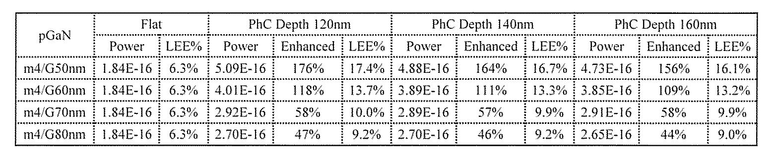
図14(a)の光取出し効率増減率では、空孔の端面から量子井戸層までの距離50nmでは、全ての深さにおいてFlatに対する強度が2.5倍以上の極大値が得られている。また、図14(c)の放射パターンでは、フォトニック結晶周期構造を有する方がFlatに対して正面方向(角度0~10°)への出力値が増大している。一方、図14(b)のFDTD法と光線追跡法のクロスシミュレーションで得られた光取出し効率では、フォトニック結晶の深さが大きくなるにつれて若干減少となっている。そこで、フォトニック結晶の深さ120nm、140nm、160nmの断面における電界強度分布を比較してみた。
In the light extraction efficiency increase / decrease rate in FIG. 14 (a), at a distance of 50 nm from the end face of the hole to the quantum well layer, a maximum value of 2.5 times or more the intensity against Flat is obtained at all depths. Further, in the radiation pattern of FIG. 14C, the output value in the front direction (
図15Aは、フォトニック結晶の深さ120nmの断面における電界強度分布である。図15Bは、フォトニック結晶の深さ140nmの断面における電界強度分布である。図15Cは、フォトニック結晶の深さ160nmの断面における電界強度分布である。図15AからCまで(電界強度分布)より、何れの深さにおいてもフォトニック結晶に侵入した光(電界)はフォトニック結晶の最深部まで到達していることがわかる。そして深さが大きくなるに従い、光(電界)がp型GaNコンタクト層に侵入していて、そこで、光が吸収・消失されることが理由として考えられる。 FIG. 15A is an electric field intensity distribution in a cross section of a photonic crystal having a depth of 120 nm. FIG. 15B is an electric field intensity distribution in a cross section of the photonic crystal having a depth of 140 nm. FIG. 15C is an electric field intensity distribution in a cross section of a photonic crystal having a depth of 160 nm. 15A to 15C (electric field intensity distribution), it can be seen that light (electric field) that has entered the photonic crystal reaches the deepest part of the photonic crystal at any depth. As the depth increases, light (electric field) penetrates into the p-type GaN contact layer, where light is absorbed and lost.
従って、p型GaNコンタクト層にフォトニック結晶を形成する場合、フォトニック結晶の深さを浅くするためにもp型GaNコンタクト層の膜厚は薄いほうが好ましい。 Therefore, when forming a photonic crystal in the p-type GaN contact layer, it is preferable that the p-type GaN contact layer is thin in order to reduce the depth of the photonic crystal.
(第5の実施の形態)
次に、本発明の第5の実施の形態に係る深紫外LEDとして、設計波長λを280nmとするAlGaN系深紫外LEDの構造を図16A(a-1)、(a-2)に示す。図16A(a-1)は断面図、図16A(a-2)は平面図である。図16B(b)は表面実装型パッケージに搭載した深紫外LEDである。
(Fifth embodiment)
Next, as a deep ultraviolet LED according to the fifth embodiment of the present invention, the structure of an AlGaN-based deep ultraviolet LED having a design wavelength λ of 280 nm is shown in FIGS. 16A (a-1) and (a-2). 16A (a-1) is a cross-sectional view, and FIG. 16A (a-2) is a plan view. FIG. 16B (b) shows a deep ultraviolet LED mounted on a surface mount package.
前記LEDは第4の実施の形態にある深紫外LEDの積層薄膜構造と同じであるが、p型GaNコンタクト層9の膜厚が150nmと異なる。これは、デバイス製造プロセス上の別の方法という観点から見た変形例となる。
The LED is the same as the laminated thin film structure of the deep ultraviolet LED in the fourth embodiment, but the thickness of the p-type
そして、p型GaNコンタクト層9とp型AlGaN層8との界面を含み、基板方向においてp型AlGaN層を超えない範囲内にフォトニック結晶周期構造100を設けており、かつ、フォトニック結晶周期構造100は、空孔(柱状構造、ホール)101(h)を設け、フォトニックバンドギャップを有することにより波長λの光を反射する反射型フォトニック結晶周期構造である。
The photonic crystal
また、空孔101(h)は、p型AlGaN層8と多重量子障壁層7の界面を超えないが、p型GaNコンタクト層9とNi層10の界面に到達した構造であり、かつ、空孔101(h)の基板方向の端面と量子井戸層5までの距離Gが、バリア層6と多重量子障壁層7の膜厚の合計値以上80nm以内にある。さらに、反射型フォトニック結晶周期構造100の深さhは、p型AlGaN層8とp型GaNコンタクト層9の膜厚の合計値以内である。
The void 101 (h) does not exceed the interface between the p-
前記構造を反映した計算モデルを作成して、FDTD法及び光線追跡法を併用して光取出し効率増減率(Enhancement of LEE)及び光取出し効率(LEE)を計算した。図17に前記p型GaNコンタクト層のフォトニック結晶計算モデルを示す。そして、解析結果を表4、図18(a)Enhancement of LEE、図18(b)光取出し効率、図18(c)放射パターン(Radiation Pattern)に示す。

図18(a)の光取出し効率増減率では、量子井戸層5から60nmの距離においてFlatに対する強度が2.5倍以上の極大値が得られている。また、図18(b)の光取出し効率においても15.7%の極大値が得られている。さらに、放射パターンでは、軸上(0~10°)の出力がFlatに対して増大している。
In the light extraction efficiency increase / decrease rate in FIG. 18 (a), a maximum value of 2.5 times or more the intensity against Flat at a distance of 60 nm from the
(第6の実施の形態)
次に、本発明の第6の実施の形態に係る深紫外LEDとして、設計波長λを280nmとするAlGaN系深紫外LEDの構造を図19A(a-1)、(a-2)に示す。図19A(a-1)は断面図、図19A(a-2)は平面図である。図19B(b)は表面実装型パッケージに搭載した深紫外LEDである。
(Sixth embodiment)
Next, as a deep ultraviolet LED according to the sixth embodiment of the present invention, the structure of an AlGaN-based deep ultraviolet LED having a design wavelength λ of 280 nm is shown in FIGS. 19A (a-1) and (a-2). 19A (a-1) is a cross-sectional view, and FIG. 19A (a-2) is a plan view. FIG. 19B (b) shows a deep ultraviolet LED mounted on a surface mount package.
前記LEDは第2の実施の形態にある深紫外LEDの積層薄膜構造と同じであるが、デバイス製造プロセス上の別の方法という観点から見た変形例となる。 The LED is the same as the laminated thin film structure of the deep ultraviolet LED in the second embodiment, but is a modification viewed from the viewpoint of another method in the device manufacturing process.
そして、p型AlGaNコンタクト層8aの膜厚が100nm以内であり、p型AlGaNコンタクト層8aに、基板方向においてp型AlGaNコンタクト層を超えない範囲内にフォトニック結晶周期構造100を設けており、かつ、フォトニック結晶周期構造100は、空孔(柱状構造、ホール)101(h)を設け、フォトニックバンドギャップを有することにより波長λの光を反射する反射型フォトニック結晶周期構造である。
The p-type
また、空孔101(h)は、p型AlGaNコンタクト層8aと多重量子障壁層7の界面を超えないが、p型AlGaNコンタクト層8aと極薄膜Ni層10aの界面に到達した構造であり、かつ、空孔101(h)の基板方向の端面と量子井戸層5までの距離Gが、バリア層6と多重量子障壁層7の膜厚の合計値以上80nm以内にある。さらに、反射型フォトニック結晶周期構造100の深さhは、p型AlGaNコンタクト層8aの膜厚以内である。
In addition, the hole 101 (h) does not exceed the interface between the p-type
前記構造を反映した計算モデルを作成して、FDTD法及び光線追跡法を併用して光取出し効率増減率(Enhancement of LEE)及び光取出し効率(LEE)を計算した。図20に前記p型AlGaNコンタクト層のフォトニック結晶計算モデルを示す。そして、解析結果を、表5、図21(a)Enhancement of LEE、図21(b)LEE、図21(c)放射パターン(Radiation Pattern)に示す。
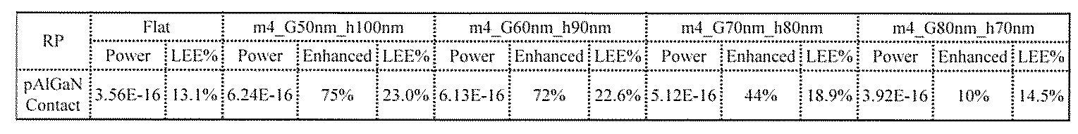
図21(a)の光取出し効率増減率では、量子井戸層5から50nmの距離においてFlatに対する強度が1.75倍と極大値が得られている。また、図21(b)の光取出し効率では、23.0%の極大値が得られている。さらに、図21(c)の放射パターンでは、軸上(0~10°)の出力がFlatに対して増大している。
In the light extraction efficiency increase / decrease rate in FIG. 21 (a), a maximum value of 1.75 times the intensity against Flat is obtained at a distance of 50 nm from the
(第7の実施の形態)
次に、本発明の第7の実施の形態に係る深紫外LEDとして、設計波長λを280nmとするAlGaN系深紫外LEDの構造を図22A(a-1)、(a-2)に示す。図22A(a-1)は断面図、図22A(a-2)は平面図である。図22B(b)は表面実装型パッケージに搭載した深紫外LEDである。
(Seventh embodiment)
Next, as a deep ultraviolet LED according to the seventh embodiment of the present invention, the structure of an AlGaN-based deep ultraviolet LED having a design wavelength λ of 280 nm is shown in FIGS. 22A (a-1) and (a-2). 22A (a-1) is a cross-sectional view, and FIG. 22A (a-2) is a plan view. FIG. 22B (b) shows a deep ultraviolet LED mounted on a surface mount package.
前記LEDは第1の実施の形態及び第4の実施の形態にある深紫外LEDの積層薄膜構造と同じであるが、フォトニック結晶周期構造100を設けている位置が異なる。これは、デバイス製造プロセス上の別の方法という観点から見た変形例となる。
The LED is the same as the laminated thin film structure of the deep ultraviolet LED in the first embodiment and the fourth embodiment, but the position where the photonic crystal
基板方向において、p型GaNコンタクト層9とp型AlGaN層8との界面を超えず、かつ、p型GaNコンタクト層9の膜厚の範囲内にフォトニック結晶周期構造100を設けており、かつ、フォトニック結晶周期構造100は、空孔(柱状構造、ホール)101(h)を設け、フォトニックバンドギャップを有することにより波長λの光を反射する反射型フォトニック結晶周期構造である。
The photonic crystal
また、空孔101(h)は、p型GaNコンタクト層9とNi層10の界面を超えず、かつ、空孔101(h)の基板方向の端面と量子井戸層5までの距離Gが、バリア層6と多重量子障壁層7の膜厚の合計値以上80nm以内にある。さらに、反射型フォトニック結晶周期構造100の深さhは、p型GaNコンタクト層9の膜厚以内である。
The hole 101 (h) does not exceed the interface between the p-type
上記の構造において、量子井戸層5で発光した波長λの深紫外光はTE光とTM光が全方向に放射されて楕円偏光しながら媒質中を伝搬する。量子井戸層5の近傍に設けられたフォトニック結晶周期構造100は、p型GaNコンタクト層9の膜厚内に設けられるため、端面においては、p型GaNコンタクト層9と空気の二つの異なる屈折率をもつ構造体として形成され、空孔の半径Rと周期aの比であるR/a=0.4とした時、上記フォトニック結晶の充填率fは次式で計算されf=2π/30.5×(R/a)2=0.58となる。
In the above structure, the deep ultraviolet light having the wavelength λ emitted from the
そして、空気の屈折率n1=1.0、p型GaNの屈折率n2=2.618、f=0.58より等価屈折率neffは次式で計算されneff=(n2 2+(n1 2-n2 2)×f)0.5=1.859が得られる。 From the refractive index of air n 1 = 1.0, the refractive index of p-type GaN n 2 = 2.618, and f = 0.58, the equivalent refractive index n eff is calculated by the following equation, and n eff = (n 2 2 + (N 1 2 −n 2 2 ) × f) 0.5 = 1.859 is obtained.
そして、発光波長λ=280nmとすると、このフォトニック結晶周期構造がブラッグ散乱条件(mλ/neff=2a、但しneff:等価屈折率、a:周期、m:次数)を満たす場合のTE光とTM光のフォトニックバンド構造を平面波展開法で求め、TE光において第1フォトニックバンドと第2フォトニックバンドの間にPBGが得られることを確認する。 Then, assuming that the emission wavelength λ = 280 nm, this photonic crystal periodic structure satisfies the Bragg scattering condition (mλ / n eff = 2a, where n eff is an equivalent refractive index, a is a period, and m is an order). The photonic band structure of TM light is obtained by the plane wave expansion method, and it is confirmed that PBG is obtained between the first photonic band and the second photonic band in TE light.
前記構造を反映した計算モデルを作成して、FDTD法及び光線追跡法を併用して光取出し効率増減率(Enhancement of LEE)及び光取出し効率(LEE)を計算した。図23に前記LED構造のフォトニック結晶計算モデルを示す。前記計算モデルは、p型AlGaN層8の膜厚を0nmから30nmの範囲で10nmステップで変化させ、空孔101(h)の位置は基板方向の端面をp型AlGaN層8とp型GaNコンタクト層9の界面から120nmの深さになるように設定した。この場合、p型AlGaN層8の膜厚が薄くなるに従い、量子井戸層5と空孔101(h)の基板方向の端面との距離Gが短くなる。すなわち、p型AlGaN層8の膜厚0nmで距離Gは50nmとなり、同様に10nmステップで変化させて、p型AlGaN層8の膜厚30nmでは距離Gが80nmとなるように設定した。この解析結果を表6、図24(a)Enhancement of LEE、図24(b)光取出し効率、図24(c)放射パターン(Radiation Pattern)を示す。
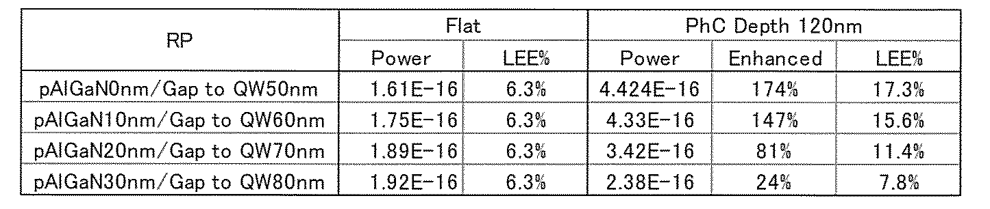
図24(a)の光取出し効率増減率では、p型AlGaN層の膜厚が薄くなるに従い、光取出し効率増減率が上がり、量子井戸層5からの距離Gが50nm(この場合のp型AlGaN層の膜厚は0nm)において強度約2.7倍の極大値が得られており、距離Gが60nm(同じく、p型AlGaN層の膜厚10nm)においても約2.5倍の強度が得られている。また、図24(b)の光取出し効率においても、距離G50nmで17.3%の極大値が得られている。さらに、図24(c)は、距離G50nmにおける放射パターンを示しており、軸上方向(0~30°)の出力がFlatに対して増大していることがわかる。
In the light extraction efficiency increase / decrease rate of FIG. 24A, the light extraction efficiency increase / decrease rate increases as the thickness of the p-type AlGaN layer decreases, and the distance G from the
以下、図1A等に示される構造を形成した後に、LEDデバイスを作成する。 Hereinafter, after forming the structure shown in FIG. 1A and the like, an LED device is created.
上記の各実施の形態による深紫外LED技術によれば、膜厚の薄いp型AlGaN層にフォトニック結晶周期構造を設けることで、 深紫外LEDのLEEを飛躍的に向上させることができる。 According to the deep ultraviolet LED technology according to each of the above embodiments, the LEE of a deep ultraviolet LED can be dramatically improved by providing a photonic crystal periodic structure in a thin p-type AlGaN layer.
上記の実施の形態において、添付図面に図示されている構成等については、これらに限定されるものではなく、本発明の効果を発揮する範囲内で適宜変更することが可能である。その他、本発明の目的の範囲を逸脱しない限りにおいて適宜変更して実施することが可能である。 In the above-described embodiment, the configuration and the like illustrated in the accompanying drawings are not limited to these, and can be changed as appropriate within the scope of the effects of the present invention. In addition, various modifications can be made without departing from the scope of the object of the present invention.
また、本発明の各構成要素は、任意に取捨選択することができ、取捨選択した構成を具備する発明も本発明に含まれるものである。 Each component of the present invention can be arbitrarily selected, and an invention having a selected configuration is also included in the present invention.
本発明は、深紫外LEDに利用可能である。 The present invention can be used for deep ultraviolet LEDs.
1…サファイア基板、2…AlNバッファー層、3…n型AlGaN層、4…バリア層、5…量子井戸層、6…バリア層、7…多重量子障壁層(MQB)、8…p型AlGaN層(透明p型AlGaN層)、8a…p型AlGaNコンタクト層(透明p型AlGaNコンタクト層)、9…p型GaNコンタクト層、10…Ni層、11…Au反射電極層。
DESCRIPTION OF
Claims (14)
反射電極層と、金属層と、p型GaNコンタクト層と、波長λに対し透明な、p型AlGaN層とを、基板とは反対側からこの順で含有する積層構造体を準備する工程と、
前記p型AlGaN層の膜厚が100nm以内で、少なくとも前記p型GaNコンタクト層と前記p型AlGaN層との界面を含み、前記基板方向において前記p型AlGaN層を超えない厚さ方向の範囲内に設けられた複数の空孔を有する反射型フォトニック結晶周期構造を有し、前記空孔の基板方向の端面から量子井戸層までの距離が前記バリア層と前記多重量子障壁層或いは前記電子ブロック層の膜厚の合計値以上80nm以内及びその深さhが前記p型AlGaN層と前記p型GaNコンタクト層の膜厚の合計値以内において光取出し効率の極大値が得られる反射型フォトニック結晶周期構造を形成するための金型を準備する工程と、
前記積層構造体上に、レジスト層を形成し、前記金型の構造を転写する工程と、
前記レジスト層をマスクとして順次前記積層構造体をエッチングしてフォトニック結晶周期構造を形成する工程と
を有する深紫外LEDの製造方法。 A method for producing a deep ultraviolet LED according to claim 1,
Preparing a laminated structure containing a reflective electrode layer, a metal layer, a p-type GaN contact layer, a p-type AlGaN layer transparent to the wavelength λ in this order from the opposite side of the substrate;
The thickness of the p-type AlGaN layer is 100 nm or less, includes at least the interface between the p-type GaN contact layer and the p-type AlGaN layer, and within a range in the thickness direction that does not exceed the p-type AlGaN layer in the substrate direction. A reflection type photonic crystal periodic structure having a plurality of holes provided in the substrate, wherein a distance from an end surface in the substrate direction of the holes to a quantum well layer is the barrier layer and the multiple quantum barrier layer or the electronic block A reflective photonic crystal in which the maximum value of the light extraction efficiency is obtained when the total thickness of the layers is within 80 nm and the depth h is within the total thickness of the p-type AlGaN layer and the p-type GaN contact layer Preparing a mold for forming a periodic structure;
Forming a resist layer on the laminated structure and transferring the structure of the mold;
And a step of sequentially etching the laminated structure using the resist layer as a mask to form a photonic crystal periodic structure.
反射電極層と、極薄膜金属層と、波長λに対し透明な、p型AlGaNコンタクト層とを、基板とは反対側からこの順で含有する積層構造体を準備する工程と、
前記p型AlGaNコンタクト層の膜厚が100nm以内で、前記p型AlGaNコンタクト層内に、前記基板方向において前記p型AlGaNコンタクト層を超えない厚さ方向の範囲内に設けられた複数の空孔を有する反射型フォトニック結晶周期構造を有し、前記空孔の基板方向の端面から量子井戸層までの距離が前記バリア層と前記多重量子障壁層或いは前記電子ブロック層の膜厚の合計値以上80nm以内及びその深さhが前記p型AlGaNコンタクト層の膜厚以内において光取出し効率の極大値が得られる反射型フォトニック結晶周期構造を形成するための金型を準備する工程と、
前記積層構造体上に、レジスト層を形成し、前記金型の構造を転写する工程と、
前記レジスト層をマスクとして順次前記積層構造体をエッチングしてフォトニック結晶周期構造を形成する工程とを有する深紫外LEDの製造方法。 A method for producing a deep ultraviolet LED according to claim 2,
Preparing a laminated structure containing a reflective electrode layer, an ultra-thin metal layer, a p-type AlGaN contact layer transparent to a wavelength λ in this order from the side opposite to the substrate;
The p-type AlGaN contact layer has a thickness of 100 nm or less, and a plurality of holes provided in the p-type AlGaN contact layer within a range in the thickness direction not exceeding the p-type AlGaN contact layer in the substrate direction The distance from the end surface of the hole in the substrate direction to the quantum well layer is equal to or greater than the total thickness of the barrier layer and the multiple quantum barrier layer or the electron blocking layer. Preparing a mold for forming a reflective photonic crystal periodic structure within 80 nm and its depth h within the film thickness of the p-type AlGaN contact layer and obtaining a maximum value of light extraction efficiency;
Forming a resist layer on the laminated structure and transferring the structure of the mold;
And a step of sequentially etching the laminated structure using the resist layer as a mask to form a photonic crystal periodic structure.
反射電極層と、金属層と、p型GaNコンタクト層と、波長λに対し透明な、p型AlGaN層とを、基板とは反対側からこの順で含有する積層構造体を準備する工程と、
前記p型AlGaN層の膜厚が100nm以内で、少なくとも前記p型GaNコンタクト層と前記p型AlGaN層との界面を含み、前記基板方向において前記p型AlGaN層を超えない厚さ方向からp型GaNコンタクト層と金属層を貫通し、反射電極層内に達しているが、反射電極層を超えない位置に設けられた複数の空孔を有する反射型フォトニック結晶周期構造を有し、前記空孔の基板方向の端面から量子井戸層までの距離が前記バリア層と前記多重量子障壁層或いは前記電子ブロック層の膜厚の合計値以上80nm以内において光取出し効率の極大値が得られる反射型フォトニック結晶周期構造を形成するための金型を準備する工程と、
前記積層構造体上に、レジスト層を形成し、前記金型の構造を転写する工程と、
前記レジスト層をマスクとして順次前記積層構造体をエッチングしてフォトニック結晶周期構造を形成する工程と、
反射電極層を再蒸着させる工程と
を有する深紫外LEDの製造方法。 A method for producing a deep ultraviolet LED according to claim 3,
Preparing a laminated structure containing a reflective electrode layer, a metal layer, a p-type GaN contact layer, a p-type AlGaN layer transparent to the wavelength λ in this order from the opposite side of the substrate;
The p-type AlGaN layer has a thickness of 100 nm or less, includes at least an interface between the p-type GaN contact layer and the p-type AlGaN layer, and is p-type from a thickness direction that does not exceed the p-type AlGaN layer in the substrate direction. It has a reflective photonic crystal periodic structure having a plurality of holes provided at a position not penetrating the GaN contact layer and the metal layer and reaching the reflective electrode layer. Reflective type photo diode that can obtain the maximum value of the light extraction efficiency when the distance from the end surface of the hole in the substrate direction to the quantum well layer is within 80 nm of the total thickness of the barrier layer and the multiple quantum barrier layer or the electron blocking layer Preparing a mold for forming a nick crystal periodic structure;
Forming a resist layer on the laminated structure and transferring the structure of the mold;
Etching the stacked structure sequentially using the resist layer as a mask to form a photonic crystal periodic structure;
A method for producing a deep ultraviolet LED, comprising the step of redepositing the reflective electrode layer.
反射電極層と、極薄膜金属層と、波長λに対し透明な、p型AlGaNコンタクト層とを、基板とは反対側からこの順で含有する積層構造体を準備する工程と、
前記p型AlGaNコンタクト層の膜厚が100nm以内で、前記基板方向において前記p型AlGaNコンタクト層を超えない厚さ方向から極薄膜金属層を貫通し、反射電極層内に達しているが反射電極層を超えない位置に設けられた複数の空孔を有する反射型フォトニック結晶周期構造を有し、前記空孔の基板方向の端面から量子井戸層までの距離が前記バリア層と前記多重量子障壁層或いは前記電子ブロック層の膜厚の合計値以上80nm以内において光取出し効率の極大値が得られる反射型フォトニック結晶周期構造を形成するための金型を準備する工程と、
前記積層構造体上に、レジスト層を形成し、前記金型の構造を転写する工程と、
前記レジスト層をマスクとして順次前記積層構造体をエッチングしてフォトニック結晶周期構造を形成する工程と、
反射電極層を再蒸着させる工程と
を有する深紫外LEDの製造方法。 A method for producing a deep ultraviolet LED according to claim 4,
Preparing a laminated structure containing a reflective electrode layer, an ultra-thin metal layer, a p-type AlGaN contact layer transparent to a wavelength λ in this order from the side opposite to the substrate;
The p-type AlGaN contact layer has a thickness of 100 nm or less, penetrates the ultrathin metal layer from the thickness direction not exceeding the p-type AlGaN contact layer in the substrate direction, and reaches the reflective electrode layer. A reflective photonic crystal periodic structure having a plurality of vacancies provided at positions not exceeding the layer, wherein the distance from the end surface in the substrate direction of the vacancies to the quantum well layer is the barrier layer and the multiple quantum barrier Preparing a mold for forming a reflective photonic crystal periodic structure capable of obtaining a maximum value of light extraction efficiency within 80 nm or more of the total thickness of the layer or the electron blocking layer;
Forming a resist layer on the laminated structure and transferring the structure of the mold;
Etching the stacked structure sequentially using the resist layer as a mask to form a photonic crystal periodic structure;
A method for producing a deep ultraviolet LED, comprising the step of redepositing the reflective electrode layer.
反射電極層と、金属層と、p型GaNコンタクト層と、波長λに対し透明な、p型AlGaN層とを、基板とは反対側からこの順で含有する積層構造体を準備する工程と、
前記p型AlGaN層の膜厚が100nm以内で、少なくとも前記p型GaNコンタクト層と前記p型AlGaN層との界面を含み、前記基板方向において前記p型AlGaN層を超えない厚さ方向からp型GaNコンタクト層と金属層の界面にかけて設けられた複数の空孔を有する反射型フォトニック結晶周期構造を有し、前記空孔の基板方向の端面から量子井戸層までの距離が前記バリア層と前記多重量子障壁層或いは前記電子ブロック層の膜厚の合計値以上80nm以内及びその深さhが前記p型AlGaN層と前記p型GaNコンタクト層の膜厚の合計値以内において光取出し効率の極大値が得られる反射型フォトニック結晶周期構造を形成するための金型を準備する工程と、
前記積層構造体のうち前記p型GaNコンタクト層まで結晶成長させた上に、レジスト層を形成し、前記金型の構造を転写する工程と、
前記レジスト層をマスクとして順次前記積層構造体をエッチングしてフォトニック結晶周期構造を形成する工程と、
前記フォトニック結晶周期構造形成後に金属層と反射電極層をこの順で斜め蒸着させる工程と
を有する深紫外LEDの製造方法。 A deep ultraviolet LED manufacturing method according to claim 5,
Preparing a laminated structure containing a reflective electrode layer, a metal layer, a p-type GaN contact layer, a p-type AlGaN layer transparent to the wavelength λ in this order from the opposite side of the substrate;
The p-type AlGaN layer has a thickness of 100 nm or less, includes at least an interface between the p-type GaN contact layer and the p-type AlGaN layer, and is p-type from a thickness direction that does not exceed the p-type AlGaN layer in the substrate direction. A reflective photonic crystal periodic structure having a plurality of holes provided over the interface between the GaN contact layer and the metal layer, and the distance from the end surface of the holes toward the quantum well layer to the quantum well layer The maximum value of light extraction efficiency when the total thickness of the multiple quantum barrier layer or the electron blocking layer is not less than 80 nm and the depth h is within the total thickness of the p-type AlGaN layer and the p-type GaN contact layer. Preparing a mold for forming a reflective photonic crystal periodic structure that provides:
Forming a resist layer on the crystal structure of the laminated structure up to the p-type GaN contact layer, and transferring the structure of the mold;
Etching the stacked structure sequentially using the resist layer as a mask to form a photonic crystal periodic structure;
A method of manufacturing a deep ultraviolet LED, comprising forming a metal layer and a reflective electrode layer obliquely in this order after forming the photonic crystal periodic structure.
反射電極層と、極薄膜金属層と、波長λに対し透明な、p型AlGaNコンタクト層とを、基板とは反対側からこの順で含有する積層構造体を準備する工程と、
前記p型AlGaNコンタクト層の膜厚が100nm以内で、前記p型AlGaNコンタクト層内に、前記基板方向において前記p型AlGaNコンタクト層を超えない厚さ方向からp型AlGaNコンタクト層と極薄膜金属層の界面にかけて設けられた複数の空孔を有する反射型フォトニック結晶周期構造を有し、前記空孔の基板方向の端面から量子井戸層までの距離が前記バリア層と前記多重量子障壁層或いは前記電子ブロック層の膜厚の合計値以上80nm以内及びその深さhが前記p型AlGaNコンタクト層の膜厚以内において光取出し効率の極大値が得られる反射型フォトニック結晶周期構造を形成するための金型を準備する工程と、
前記積層構造体のうち前記p型AlGaNコンタクト層まで結晶成長させた上に、レジスト層を形成し、前記金型の構造を転写する工程と、
前記レジスト層をマスクとして順次前記積層構造体をエッチングしてフォトニック結晶周期構造を形成する工程と、
前記フォトニック結晶周期構造形成後に極薄膜金属層と反射電極層をこの順で斜め蒸着させる工程と
を有する深紫外LEDの製造方法。 A method for producing a deep ultraviolet LED according to claim 6,
Preparing a laminated structure containing a reflective electrode layer, an ultra-thin metal layer, a p-type AlGaN contact layer transparent to a wavelength λ in this order from the side opposite to the substrate;
The p-type AlGaN contact layer has a thickness of 100 nm or less, and the p-type AlGaN contact layer and the ultrathin metal layer are formed in the p-type AlGaN contact layer from the thickness direction not exceeding the p-type AlGaN contact layer in the substrate direction. A reflective photonic crystal periodic structure having a plurality of vacancies provided over the interface, and the distance from the end surface of the vacancies in the substrate direction to the quantum well layer is the barrier layer and the multiple quantum barrier layer or the For forming a reflective photonic crystal periodic structure in which the maximum value of the light extraction efficiency is obtained when the total thickness of the electron blocking layer is not less than 80 nm and the depth h is within the thickness of the p-type AlGaN contact layer. Preparing the mold,
Forming a resist layer on the crystal structure of the laminated structure up to the p-type AlGaN contact layer, and transferring the mold structure;
Etching the stacked structure sequentially using the resist layer as a mask to form a photonic crystal periodic structure;
A method of manufacturing a deep ultraviolet LED, comprising: forming an ultrathin metal layer and a reflective electrode layer obliquely in this order after forming the photonic crystal periodic structure.
反射電極層と、金属層と、p型GaNコンタクト層と、波長λに対し透明な、p型AlGaN層とを、基板とは反対側からこの順で含有する積層構造体を準備する工程と、前記p型AlGaN層の膜厚が100nm以内で、前記p型GaNコンタクト層と前記p型AlGaN層との界面を超えず、かつ、前記基板方向において前記p型GaNコンタクト層の膜厚の範囲内に設けられた複数の空孔を有する反射型フォトニック結晶周期構造を有し、前記空孔の基板方向の端面から量子井戸層までの距離が前記バリア層と前記多重量子障壁層或いは前記電子ブロック層の膜厚の合計値以上80nm以内及びその深さhが前記p型GaNコンタクト層の膜厚以内において光取出し効率の極大値が得られる反射型フォトニック結晶周期構造を形成するための金型を準備する工程と、前記積層構造体のうち前記p型GaNコンタクト層まで結晶成長させた上に、レジスト層を形成し、前記金型の構造を転写する工程と、前記レジスト層をマスクとして順次前記積層構造体をエッチングしてフォトニック結晶周期構造を形成する工程と、を有する深紫外LEDの製造方法。 It is a manufacturing method of the deep ultraviolet LED according to claim 7,
Preparing a laminated structure containing a reflective electrode layer, a metal layer, a p-type GaN contact layer, a p-type AlGaN layer transparent to the wavelength λ in this order from the opposite side of the substrate; The thickness of the p-type AlGaN layer is within 100 nm, does not exceed the interface between the p-type GaN contact layer and the p-type AlGaN layer, and is within the range of the thickness of the p-type GaN contact layer in the substrate direction. A reflection type photonic crystal periodic structure having a plurality of holes provided in the substrate, wherein a distance from an end surface in the substrate direction of the holes to a quantum well layer is the barrier layer and the multiple quantum barrier layer or the electronic block A reflective photonic crystal periodic structure is formed in which the maximum value of the light extraction efficiency is obtained when the total thickness of the layers is within 80 nm and the depth h is within the thickness of the p-type GaN contact layer. A step of preparing a metal mold, a step of crystal growth up to the p-type GaN contact layer in the stacked structure, a step of forming a resist layer, and transferring the structure of the mold; and the resist layer And a step of sequentially etching the laminated structure using the mask as a mask to form a photonic crystal periodic structure.
Priority Applications (5)
| Application Number | Priority Date | Filing Date | Title |
|---|---|---|---|
| KR1020177013240A KR101811819B1 (en) | 2016-03-30 | 2016-11-01 | Deep ultraviolet LED and method for manufacturing the same |
| JP2017517135A JP6156898B1 (en) | 2016-03-30 | 2016-11-01 | Deep ultraviolet LED and manufacturing method thereof |
| CN201680003179.3A CN107534072B (en) | 2016-03-30 | 2016-11-01 | Deep ultraviolet LED and its manufacturing method |
| US15/526,860 US10056526B2 (en) | 2016-03-30 | 2016-11-01 | Deep ultraviolet LED and method for manufacturing the same |
| EP16861100.2A EP3249701B1 (en) | 2016-03-30 | 2016-11-01 | Deep ultraviolet led and production method therefor |
Applications Claiming Priority (2)
| Application Number | Priority Date | Filing Date | Title |
|---|---|---|---|
| JP2016069434 | 2016-03-30 | ||
| JP2016-069434 | 2016-03-30 |
Publications (1)
| Publication Number | Publication Date |
|---|---|
| WO2017168811A1 true WO2017168811A1 (en) | 2017-10-05 |
Family
ID=59014415
Family Applications (1)
| Application Number | Title | Priority Date | Filing Date |
|---|---|---|---|
| PCT/JP2016/082397 Ceased WO2017168811A1 (en) | 2016-03-30 | 2016-11-01 | Deep ultraviolet led and production method therefor |
Country Status (6)
| Country | Link |
|---|---|
| US (1) | US10056526B2 (en) |
| EP (1) | EP3249701B1 (en) |
| KR (1) | KR101811819B1 (en) |
| CN (1) | CN107534072B (en) |
| TW (1) | TWI634674B (en) |
| WO (1) | WO2017168811A1 (en) |
Cited By (5)
| Publication number | Priority date | Publication date | Assignee | Title |
|---|---|---|---|---|
| WO2019146737A1 (en) * | 2018-01-26 | 2019-08-01 | 丸文株式会社 | Deep ultraviolet led and production method for same |
| WO2020040304A1 (en) * | 2018-08-24 | 2020-02-27 | 丸文株式会社 | Deep ultraviolet led device and method for manufacturing same |
| WO2020138146A1 (en) * | 2018-12-28 | 2020-07-02 | 丸文株式会社 | Deep ultraviolet led device and manufacturing method therefor |
| JP2021097148A (en) * | 2019-12-18 | 2021-06-24 | 日機装株式会社 | Semiconductor light-emitting element |
| JP2021174876A (en) * | 2020-04-24 | 2021-11-01 | 日機装株式会社 | Semiconductor light-emitting device and method for manufacturing the same |
Families Citing this family (4)
| Publication number | Priority date | Publication date | Assignee | Title |
|---|---|---|---|---|
| EP3346509B1 (en) | 2015-09-03 | 2021-06-30 | Marubun Corporation | Deep-ultraviolet led and method for manufacturing same |
| CN110197839B (en) * | 2018-06-15 | 2021-08-03 | 京东方科技集团股份有限公司 | Double-sided display panel and preparation method thereof, and double-sided display device |
| CN111106212A (en) * | 2019-12-26 | 2020-05-05 | 南京亮芯信息科技有限公司 | Deep ultraviolet light-emitting diode with vertical structure and preparation method thereof |
| CN118156389B (en) * | 2024-05-13 | 2024-08-02 | 江西乾照光电有限公司 | A white light LED epitaxial wafer, epitaxial growth method and LED chip |
Citations (5)
| Publication number | Priority date | Publication date | Assignee | Title |
|---|---|---|---|---|
| WO2011104969A1 (en) * | 2010-02-24 | 2011-09-01 | 独立行政法人理化学研究所 | Light-emitting element having nitride semiconductor multiquantum barrier, and process for production thereof |
| JP2013120829A (en) * | 2011-12-07 | 2013-06-17 | Sharp Corp | Nitride semiconductor ultraviolet light-emitting device |
| JP2013530537A (en) * | 2010-06-18 | 2013-07-25 | センサー エレクトロニック テクノロジー インコーポレイテッド | Deep ultraviolet light emitting diode |
| WO2015008776A1 (en) * | 2013-07-17 | 2015-01-22 | 丸文株式会社 | Semiconductor light-emitting element and production method |
| JP5757512B1 (en) | 2014-03-06 | 2015-07-29 | 丸文株式会社 | Deep ultraviolet LED and manufacturing method thereof |
Family Cites Families (73)
| Publication number | Priority date | Publication date | Assignee | Title |
|---|---|---|---|---|
| US5337328A (en) | 1992-05-08 | 1994-08-09 | Sdl, Inc. | Semiconductor laser with broad-area intra-cavity angled grating |
| US5955749A (en) | 1996-12-02 | 1999-09-21 | Massachusetts Institute Of Technology | Light emitting device utilizing a periodic dielectric structure |
| EP1378949A4 (en) | 2001-03-21 | 2006-03-22 | Mitsubishi Cable Ind Ltd | Semiconductor light-emitting device |
| JP3991612B2 (en) | 2001-04-09 | 2007-10-17 | 日亜化学工業株式会社 | Light emitting element |
| US6936854B2 (en) | 2001-05-10 | 2005-08-30 | Canon Kabushiki Kaisha | Optoelectronic substrate |
| US7194174B2 (en) | 2001-10-19 | 2007-03-20 | Ignis Technologies As | Integrated photonic crystal structure and method of producing same |
| US6878969B2 (en) | 2002-07-29 | 2005-04-12 | Matsushita Electric Works, Ltd. | Light emitting device |
| JP4329374B2 (en) | 2002-07-29 | 2009-09-09 | パナソニック電工株式会社 | LIGHT EMITTING ELEMENT AND MANUFACTURING METHOD THEREOF |
| JP2004200209A (en) | 2002-12-16 | 2004-07-15 | Fuji Xerox Co Ltd | Method of forming conductive patterns such as electrodes, surface emitting semiconductor laser using the same, and method of manufacturing the same |
| JP4610863B2 (en) | 2003-03-19 | 2011-01-12 | フィリップス ルミレッズ ライティング カンパニー リミテッド ライアビリティ カンパニー | Improved LED efficiency using photonic crystal structure |
| JP4317375B2 (en) | 2003-03-20 | 2009-08-19 | 株式会社日立製作所 | Nanoprint apparatus and fine structure transfer method |
| US7083993B2 (en) | 2003-04-15 | 2006-08-01 | Luminus Devices, Inc. | Methods of making multi-layer light emitting devices |
| US7367691B2 (en) | 2003-06-16 | 2008-05-06 | Industrial Technology Research Institute | Omnidirectional one-dimensional photonic crystal and light emitting device made from the same |
| US7683377B2 (en) | 2003-07-16 | 2010-03-23 | Panasonic Corporation | Semiconductor light emitting device, method of manufacturing the same, and lighting apparatus and display apparatus using the same |
| US7012279B2 (en) | 2003-10-21 | 2006-03-14 | Lumileds Lighting U.S., Llc | Photonic crystal light emitting device |
| US20070267646A1 (en) | 2004-06-03 | 2007-11-22 | Philips Lumileds Lighting Company, Llc | Light Emitting Device Including a Photonic Crystal and a Luminescent Ceramic |
| JP2008521211A (en) | 2004-07-24 | 2008-06-19 | ヨン ラグ ト | LED device including thin-film phosphor having two-dimensional nano-periodic structure |
| US20060043400A1 (en) | 2004-08-31 | 2006-03-02 | Erchak Alexei A | Polarized light emitting device |
| JP2006196658A (en) | 2005-01-13 | 2006-07-27 | Matsushita Electric Ind Co Ltd | Semiconductor light emitting device and manufacturing method thereof |
| JP2006276388A (en) | 2005-03-29 | 2006-10-12 | Alps Electric Co Ltd | Photonic crystal slab, photonic crystal waveguide and optical device |
| US8101498B2 (en) | 2005-04-21 | 2012-01-24 | Pinnington Thomas Henry | Bonded intermediate substrate and method of making same |
| JP4027393B2 (en) * | 2005-04-28 | 2007-12-26 | キヤノン株式会社 | Surface emitting laser |
| US7592637B2 (en) | 2005-06-17 | 2009-09-22 | Goldeneye, Inc. | Light emitting diodes with reflective electrode and side electrode |
| US8163575B2 (en) * | 2005-06-17 | 2012-04-24 | Philips Lumileds Lighting Company Llc | Grown photonic crystals in semiconductor light emitting devices |
| TWI253771B (en) | 2005-07-25 | 2006-04-21 | Formosa Epitaxy Inc | Light emitting diode structure |
| JP2007109689A (en) | 2005-10-11 | 2007-04-26 | Seiko Epson Corp | LIGHT EMITTING DEVICE, LIGHT EMITTING DEVICE MANUFACTURING METHOD, AND IMAGE DISPLAY DEVICE |
| US7679098B2 (en) | 2006-01-30 | 2010-03-16 | Avago Technologies Ecbu Ip (Singapore) Pte. Ltd. | Highly directional light emitting diode using photonic bandgap waveguides |
| US7687811B2 (en) | 2006-03-21 | 2010-03-30 | Lg Electronics Inc. | Vertical light emitting device having a photonic crystal structure |
| JP2007294789A (en) | 2006-04-27 | 2007-11-08 | Sony Corp | Semiconductor laser element |
| KR100736623B1 (en) | 2006-05-08 | 2007-07-09 | 엘지전자 주식회사 | Vertical light emitting device and manufacturing method |
| JP4231880B2 (en) | 2006-07-26 | 2009-03-04 | 株式会社東芝 | Three-dimensional structure, light emitting device having the same, and method for manufacturing the same |
| JP2008053425A (en) | 2006-08-24 | 2008-03-06 | Matsushita Electric Ind Co Ltd | Semiconductor light emitting device |
| US7829905B2 (en) | 2006-09-07 | 2010-11-09 | Hong Kong Applied Science And Technology Research Institute Co., Ltd. | Semiconductor light emitting device |
| US7697584B2 (en) | 2006-10-02 | 2010-04-13 | Philips Lumileds Lighting Company, Llc | Light emitting device including arrayed emitters defined by a photonic crystal |
| JP2008098526A (en) | 2006-10-13 | 2008-04-24 | Toyoda Gosei Co Ltd | Light-emitting element |
| JP2008117922A (en) * | 2006-11-02 | 2008-05-22 | Yamaguchi Univ | Semiconductor light emitting device and manufacturing method thereof |
| KR100886821B1 (en) | 2007-05-29 | 2009-03-04 | 한국광기술원 | Photonic Crystal Light Emitting Device with Improved Electrical Characteristics and Manufacturing Method |
| JP2008311317A (en) | 2007-06-12 | 2008-12-25 | Eudyna Devices Inc | Semiconductor light-emitting element |
| KR101341374B1 (en) | 2007-07-30 | 2013-12-16 | 삼성전자주식회사 | Photonic crystal light emitting device and manufacturing method of the same |
| JP4408443B2 (en) | 2007-08-01 | 2010-02-03 | 株式会社日立製作所 | Rotating electric machine |
| JP2009267263A (en) | 2008-04-28 | 2009-11-12 | Kyocera Corp | Light-emitting device and method for manufacturing the same |
| KR100933529B1 (en) | 2008-05-28 | 2009-12-23 | 재단법인서울대학교산학협력재단 | Light-Emitting Device with Photonic Crystal Structure |
| EP2286980A4 (en) | 2008-06-05 | 2011-07-13 | Asahi Glass Co Ltd | NANO-PRINTING MOLD, METHOD FOR MANUFACTURING THE SAME, AND PROCESSES FOR PRODUCING A MOLDED RESIN HAVING A FINE ROUGH STRUCTURE ON A SURFACE AND FOR PRODUCING A METAL GRID POLARIZER |
| JP5282503B2 (en) | 2008-09-19 | 2013-09-04 | 日亜化学工業株式会社 | Semiconductor light emitting device |
| JP5379434B2 (en) | 2008-09-22 | 2013-12-25 | 学校法人 名城大学 | Method for manufacturing sapphire substrate for light emitting device |
| JP4892025B2 (en) | 2008-09-26 | 2012-03-07 | 株式会社東芝 | Imprint method |
| KR101040462B1 (en) | 2008-12-04 | 2011-06-09 | 엘지이노텍 주식회사 | Light emitting device and manufacturing method |
| SG171832A1 (en) | 2008-12-05 | 2011-07-28 | Asahi Glass Co Ltd | Photocurable composition and method for manufacturing a molded body having a fine surface pattern |
| GB0902569D0 (en) | 2009-02-16 | 2009-04-01 | Univ Southampton | An optical device |
| KR100999713B1 (en) | 2009-03-17 | 2010-12-08 | 엘지이노텍 주식회사 | Light emitting device and manufacturing method |
| JP5300078B2 (en) | 2009-10-19 | 2013-09-25 | 国立大学法人京都大学 | Photonic crystal light emitting diode |
| WO2011049018A1 (en) | 2009-10-23 | 2011-04-28 | 日本電気株式会社 | Light emitting element and projection display device provided with same |
| DE102009057780A1 (en) | 2009-12-10 | 2011-06-16 | Osram Opto Semiconductors Gmbh | Optoelectronic semiconductor component and photonic crystal |
| JP5549338B2 (en) | 2010-04-09 | 2014-07-16 | ウシオ電機株式会社 | Nitrogen compound semiconductor LED for ultraviolet light radiation and method for producing the same |
| JP5331051B2 (en) | 2010-04-21 | 2013-10-30 | パナソニック株式会社 | Light emitting element |
| US9130348B2 (en) | 2010-07-30 | 2015-09-08 | Kyoto University | Two-dimensional photonic crystal laser |
| CN103221740B (en) | 2010-11-18 | 2015-02-25 | 日本电气株式会社 | Light source unit and projection display device provided with same |
| JP5620827B2 (en) | 2011-01-06 | 2014-11-05 | 富士フイルム株式会社 | Cleaning method of nanoimprint mold |
| KR20120092325A (en) | 2011-02-11 | 2012-08-21 | 서울옵토디바이스주식회사 | Light emitting diode having photonic crystal structure and method of fabricating the same |
| KR20120092326A (en) * | 2011-02-11 | 2012-08-21 | 서울옵토디바이스주식회사 | Non-polar light emitting diode having photonic crystal structure and method of fabricating the same |
| JP5678728B2 (en) | 2011-03-03 | 2015-03-04 | 大日本印刷株式会社 | Mold and manufacturing method thereof |
| JP2012186414A (en) | 2011-03-08 | 2012-09-27 | Toshiba Corp | Light-emitting device |
| JP5715686B2 (en) | 2011-03-23 | 2015-05-13 | 創光科学株式会社 | Nitride semiconductor ultraviolet light emitting device |
| BR112013026132A8 (en) | 2011-06-23 | 2017-12-05 | Asahi Chemical Ind | PRODUCT IN LAYERS FOR FORMING A FINE PATTERN, METHODS OF MANUFACTURING THE SAME, OF MANUFACTURING A STRUCTURE OF A FINE PATTERN, A LIGHT-EMITTING SEMICONDUCTOR DEVICE, AND A FINE PATTERN |
| US20130009167A1 (en) | 2011-07-06 | 2013-01-10 | Sharp Kabushiki Kaisha | Light emitting diode with patterned structures and method of making the same |
| US9349918B2 (en) | 2011-07-12 | 2016-05-24 | Marubun Corporation | Light emitting element and method for manufacturing same |
| JP2013042079A (en) | 2011-08-19 | 2013-02-28 | Sharp Corp | Semiconductor light emitting device |
| CN103597619B (en) | 2012-03-07 | 2015-10-14 | 株式会社爱发科 | The method of manufacturing installation |
| US20150044417A1 (en) | 2012-03-12 | 2015-02-12 | Asahi Kasei E-Materials Corporation | Mold, resist layered product, manufacturing method of the product, and concavo-convex structure product |
| KR102059030B1 (en) | 2012-09-24 | 2019-12-24 | 엘지이노텍 주식회사 | Ultraviolet light emitting device |
| CN103165771B (en) | 2013-03-28 | 2015-07-15 | 天津三安光电有限公司 | Nitride bottom layer with embedded hole structure and preparation method of nitride bottom layer |
| JP2015041763A (en) | 2013-08-20 | 2015-03-02 | 正幸 安部 | Optical semiconductor device and manufacturing method of the same |
| WO2016113935A1 (en) | 2015-01-16 | 2016-07-21 | 丸文株式会社 | Deep ultraviolet led and method for manufacturing same |
-
2016
- 2016-11-01 WO PCT/JP2016/082397 patent/WO2017168811A1/en not_active Ceased
- 2016-11-01 EP EP16861100.2A patent/EP3249701B1/en active Active
- 2016-11-01 US US15/526,860 patent/US10056526B2/en active Active
- 2016-11-01 KR KR1020177013240A patent/KR101811819B1/en active Active
- 2016-11-01 CN CN201680003179.3A patent/CN107534072B/en active Active
-
2017
- 2017-02-03 TW TW106103640A patent/TWI634674B/en active
Patent Citations (6)
| Publication number | Priority date | Publication date | Assignee | Title |
|---|---|---|---|---|
| WO2011104969A1 (en) * | 2010-02-24 | 2011-09-01 | 独立行政法人理化学研究所 | Light-emitting element having nitride semiconductor multiquantum barrier, and process for production thereof |
| JP2013530537A (en) * | 2010-06-18 | 2013-07-25 | センサー エレクトロニック テクノロジー インコーポレイテッド | Deep ultraviolet light emitting diode |
| JP2013120829A (en) * | 2011-12-07 | 2013-06-17 | Sharp Corp | Nitride semiconductor ultraviolet light-emitting device |
| WO2015008776A1 (en) * | 2013-07-17 | 2015-01-22 | 丸文株式会社 | Semiconductor light-emitting element and production method |
| JP2015195388A (en) * | 2013-07-17 | 2015-11-05 | 丸文株式会社 | Method of calculating parameter of photonic crystal periodic structure, program, and recording medium |
| JP5757512B1 (en) | 2014-03-06 | 2015-07-29 | 丸文株式会社 | Deep ultraviolet LED and manufacturing method thereof |
Non-Patent Citations (2)
| Title |
|---|
| HIDEKI HIRAYAMA ET AL.: "Recent progress and future prospects of AlGaN-based high- efficiency deep-ultraviolet light-emitting", JAPANESE JOURNAL OF APPLIED PHYSICS, vol. 53, no. 10, 17 September 2014 (2014-09-17), pages 100209-1 - 100209-10, XP055404492 * |
| See also references of EP3249701A4 |
Cited By (9)
| Publication number | Priority date | Publication date | Assignee | Title |
|---|---|---|---|---|
| WO2019146737A1 (en) * | 2018-01-26 | 2019-08-01 | 丸文株式会社 | Deep ultraviolet led and production method for same |
| JPWO2019146737A1 (en) * | 2018-01-26 | 2021-01-07 | 丸文株式会社 | Deep UV LED and its manufacturing method |
| US11309454B2 (en) | 2018-01-26 | 2022-04-19 | Marubun Corporation | Deep ultraviolet LED and method for producing the same |
| JP7316610B2 (en) | 2018-01-26 | 2023-07-28 | 丸文株式会社 | Deep UV LED and its manufacturing method |
| JP7316610B6 (en) | 2018-01-26 | 2024-02-19 | 丸文株式会社 | Deep ultraviolet LED and its manufacturing method |
| WO2020040304A1 (en) * | 2018-08-24 | 2020-02-27 | 丸文株式会社 | Deep ultraviolet led device and method for manufacturing same |
| WO2020138146A1 (en) * | 2018-12-28 | 2020-07-02 | 丸文株式会社 | Deep ultraviolet led device and manufacturing method therefor |
| JP2021097148A (en) * | 2019-12-18 | 2021-06-24 | 日機装株式会社 | Semiconductor light-emitting element |
| JP2021174876A (en) * | 2020-04-24 | 2021-11-01 | 日機装株式会社 | Semiconductor light-emitting device and method for manufacturing the same |
Also Published As
| Publication number | Publication date |
|---|---|
| KR101811819B1 (en) | 2017-12-22 |
| EP3249701B1 (en) | 2020-07-08 |
| EP3249701A1 (en) | 2017-11-29 |
| CN107534072A (en) | 2018-01-02 |
| TWI634674B (en) | 2018-09-01 |
| US10056526B2 (en) | 2018-08-21 |
| CN107534072B (en) | 2019-04-19 |
| EP3249701A4 (en) | 2017-11-29 |
| US20180198026A1 (en) | 2018-07-12 |
| TW201735393A (en) | 2017-10-01 |
Similar Documents
| Publication | Publication Date | Title |
|---|---|---|
| WO2017168811A1 (en) | Deep ultraviolet led and production method therefor | |
| TWI608631B (en) | Deep ultraviolet LED and its manufacturing method | |
| US10950751B2 (en) | Deep ultraviolet LED and method for manufacturing the same | |
| JP7316610B2 (en) | Deep UV LED and its manufacturing method | |
| HK1214407A1 (en) | Led element and method for producing same | |
| TW201535782A (en) | Deep ultraviolet LED and its manufacturing method | |
| JP2020107778A (en) | Deep ultraviolet LED device and manufacturing method thereof | |
| JP2017063099A (en) | Manufacturing method of substrate including uneven structure and manufacturing method of semiconductor light emitting device | |
| KR101317632B1 (en) | Nitride light emitting device and method of making the same | |
| JP6156898B1 (en) | Deep ultraviolet LED and manufacturing method thereof | |
| Shin et al. | High efficiency GaN light-emitting diodes with two dimensional photonic crystal structures of deep-hole square lattices | |
| TW201501351A (en) | Light-emitting diode manufacturing method | |
| WO2020040304A1 (en) | Deep ultraviolet led device and method for manufacturing same | |
| TW201712890A (en) | Method of manufacturing light-emitting element | |
| Chavoor et al. | Light extraction improvement of GaN LEDs using nano-scale top transmission gratings | |
| CN120603403A (en) | A deep ultraviolet LED structure and preparation method thereof | |
| CN120167147A (en) | Deep UV LED | |
| WO2025058022A1 (en) | Algan-based deep ultraviolet led and method for manufacturing the same |
Legal Events
| Date | Code | Title | Description |
|---|---|---|---|
| ENP | Entry into the national phase |
Ref document number: 2017517135 Country of ref document: JP Kind code of ref document: A |
|
| REEP | Request for entry into the european phase |
Ref document number: 2016861100 Country of ref document: EP |
|
| WWE | Wipo information: entry into national phase |
Ref document number: 15526860 Country of ref document: US |
|
| 121 | Ep: the epo has been informed by wipo that ep was designated in this application |
Ref document number: 16861100 Country of ref document: EP Kind code of ref document: A1 |
|
| NENP | Non-entry into the national phase |
Ref country code: DE |