EP1091406A2 - Multilayer Interconnection board for semiconductor device, method of forming the same and mounting the semiconductor chip thereon - Google Patents
Multilayer Interconnection board for semiconductor device, method of forming the same and mounting the semiconductor chip thereon Download PDFInfo
- Publication number
- EP1091406A2 EP1091406A2 EP00121265A EP00121265A EP1091406A2 EP 1091406 A2 EP1091406 A2 EP 1091406A2 EP 00121265 A EP00121265 A EP 00121265A EP 00121265 A EP00121265 A EP 00121265A EP 1091406 A2 EP1091406 A2 EP 1091406A2
- Authority
- EP
- European Patent Office
- Prior art keywords
- thin film
- interconnection board
- interconnection
- semiconductor device
- metal thin
- Prior art date
- Legal status (The legal status is an assumption and is not a legal conclusion. Google has not performed a legal analysis and makes no representation as to the accuracy of the status listed.)
- Withdrawn
Links
Images


Classifications
-
- H10W42/121—
-
- H10W70/60—
-
- H—ELECTRICITY
- H05—ELECTRIC TECHNIQUES NOT OTHERWISE PROVIDED FOR
- H05K—PRINTED CIRCUITS; CASINGS OR CONSTRUCTIONAL DETAILS OF ELECTRIC APPARATUS; MANUFACTURE OF ASSEMBLAGES OF ELECTRICAL COMPONENTS
- H05K3/00—Apparatus or processes for manufacturing printed circuits
- H05K3/46—Manufacturing multilayer circuits
- H05K3/4644—Manufacturing multilayer circuits by building the multilayer layer by layer, i.e. build-up multilayer circuits
- H05K3/467—Adding a circuit layer by thin film methods
-
- H—ELECTRICITY
- H05—ELECTRIC TECHNIQUES NOT OTHERWISE PROVIDED FOR
- H05K—PRINTED CIRCUITS; CASINGS OR CONSTRUCTIONAL DETAILS OF ELECTRIC APPARATUS; MANUFACTURE OF ASSEMBLAGES OF ELECTRICAL COMPONENTS
- H05K3/00—Apparatus or processes for manufacturing printed circuits
- H05K3/46—Manufacturing multilayer circuits
- H05K3/4644—Manufacturing multilayer circuits by building the multilayer layer by layer, i.e. build-up multilayer circuits
- H05K3/4682—Manufacture of core-less build-up multilayer circuits on a temporary carrier or on a metal foil
-
- H10P72/74—
-
- H10W70/095—
-
- H10W70/635—
-
- H10W70/685—
-
- H10W74/114—
-
- H10W90/701—
-
- H—ELECTRICITY
- H05—ELECTRIC TECHNIQUES NOT OTHERWISE PROVIDED FOR
- H05K—PRINTED CIRCUITS; CASINGS OR CONSTRUCTIONAL DETAILS OF ELECTRIC APPARATUS; MANUFACTURE OF ASSEMBLAGES OF ELECTRICAL COMPONENTS
- H05K3/00—Apparatus or processes for manufacturing printed circuits
- H05K3/10—Apparatus or processes for manufacturing printed circuits in which conductive material is applied to the insulating support in such a manner as to form the desired conductive pattern
- H05K3/20—Apparatus or processes for manufacturing printed circuits in which conductive material is applied to the insulating support in such a manner as to form the desired conductive pattern by affixing prefabricated conductor pattern
-
- H10P72/7424—
-
- H10P72/7438—
-
- H10W72/0198—
-
- H10W72/07204—
-
- H10W72/07207—
-
- H10W72/877—
-
- H10W74/142—
-
- H10W74/15—
-
- H10W90/724—
-
- H10W90/734—
-
- H10W90/736—
-
- Y—GENERAL TAGGING OF NEW TECHNOLOGICAL DEVELOPMENTS; GENERAL TAGGING OF CROSS-SECTIONAL TECHNOLOGIES SPANNING OVER SEVERAL SECTIONS OF THE IPC; TECHNICAL SUBJECTS COVERED BY FORMER USPC CROSS-REFERENCE ART COLLECTIONS [XRACs] AND DIGESTS
- Y10—TECHNICAL SUBJECTS COVERED BY FORMER USPC
- Y10S—TECHNICAL SUBJECTS COVERED BY FORMER USPC CROSS-REFERENCE ART COLLECTIONS [XRACs] AND DIGESTS
- Y10S438/00—Semiconductor device manufacturing: process
- Y10S438/977—Thinning or removal of substrate
Definitions
- the present invention relates to an interconnection board, a semiconductor device having an interconnection board, a method of forming the interconnection board and a method of mounting the semiconductor chip on the interconnection board, and more particularly to a multilayer interconnection board for allowing a flip-chip semiconductor chip to be mounted thereon, a semiconductor device having a multilayer interconnection board, a method of forming the multilayer interconnection board and a method of mounting the flip-chip semiconductor chip on the multilayer interconnection board.
- FIG. 1 is a schematic cross sectional elevation view illustrative of a flip-chip semiconductor chip.
- a flip-chip semiconductor chip 101 has a first surface which further has a predetermined area array of external terminals not illustrated on a peripheral area thereof and/or an active region thereof.
- Bumps 102 are provided on the external terminals.
- the bumps 102 are made of a metal material such as a solder material, Au, Sn-Ag based alloy.
- FIG. 2 is a schematic cross sectional elevation view illustrative of a flip-chip semiconductor chip mounted on a multilayer interconnection board.
- a multilayer interconnection board 103 has electrode pads which patterns correspond to patterns of the bumps 102 of the flip-chip semiconductor chip 101.
- the flip-chip semiconductor chip 101 is mounted on the multilayer interconnection board 103. If the bumps 102 are made of a solder material, an IR re-flow process using a flux is used for mounting the flip-chip semiconductor chip 101 on the multilayer interconnection board 103.
- the multilayer interconnection board 103 mounted with the flip-chip semiconductor chip 101 is further mounted on a circuit board through external terminals which are not illustrated.
- the multilayer interconnection board 103 is different in linear expansion coefficient from the flip-chip semiconductor chip 101.
- the above conventional technique is disadvantageous in deteriorated mounting reliability, particularly deteriorated temperature cycle characteristics.
- the following two conventional techniques have been proposed.
- the first technique is to use, for the multilayer interconnection board, a ceramic-based material having a small difference in linear expansion coefficient from silicon of the flip-chip semiconductor chip 101.
- the use of the ceramic-based material is effective in improvement in reliability of mounting the flip-chip semiconductor chip 101 on the multilayer interconnection board 103, but disadvantageous as the ceramic-based material is expensive.
- the application of this conventional technique is limited to supercomputers and large scale computers.
- the second technique is to use, for the multilayer interconnection board, an organic material which is inexpensive but is larger in linear expansion coefficient than silicon of the flip-chip semiconductor chip.
- an under-fill resin is provided between the semiconductor chip and the multilayer interconnection board, so that a shearing stress of the bumps between the semiconductor chip and the multilayer interconnection board is distributed or dispersed to the under-fill resin which covers the bumps, thereby to improve the reliability.
- the multilayer interconnection board may be a build-up board in view of a minimum pitch of bump array patterns and the number of pins.
- FIGS. 3A through 3F are fragmentary cross sectional elevation views illustrative of build-up boards as the multilayer interconnection boards in sequential steps involved in a conventional fabrication method.
- a glass epoxy base material board 104 typically FR4, FR5 or BT board, is prepared.
- Cu-foils 105 having a thickness in the range of 10-40 micrometers arc adhered on both surfaces of the glass epoxy base material hoard 104.
- the Cu-foils 105 are then patterned to form Cu-interconnection patterns 105 on both surfaces of the glass epoxy base material board 104.
- a penetrating hole is made to the glass epoxy base material board 104 by a drilling process and then the penetrating hole is then plated thereby to form a plated through hole 106 which penetrates the glass epoxy base material board 104 and electrically connecting the Cu-interconnection patterns 105.
- An insulative resin filler is filled to the plated through hole 106, whereby a core board 107 is completed.
- insulating resin material layers 108 are formed over the both surfaces of the glass epoxy base material board 104 so that the insulating resin material layers 108 cover the Cu-interconnection patterns 105.
- An opening 109 is selectively formed in the insulating resin material layers 108 by a photo-lithography technique or a laser beam process, so that a part of the Cu-interconnection patterns 105 is shown through the opening 109.
- metal thin film layers 110 are entirely formed by a sputtering method or a Cu-electroless plating process, so that the metal thin film layers 110 extend on the insulating resin material layers 108 and in the opening 109, whereby the metal thin film layers 110 are electrically connected with the Cu-interconnection patterns 105.
- photo-resist films 111 having a thickness in the range of 20-40 micrometers or dry films are formed over the metal thin film layers 110.
- the photo-resist films 111 or the dry films are patterned by exposure and subsequent development processes thereby to form photo-resist patterns 111 or dry film patterns on the metal thin film layers 110.
- a selective Cu-electroplating process is carried out by use of the photo-resist patterns 111 or the dry film patterns as masks and also use of the metal thin film layers 110 as an electric supply line, thereby to selectively form interconnection patterns 112.
- the photo-resist patterns 111 or the dry film patterns are removed.
- a selective wet etching process to the metal thin film layers 110 is carried out by use of the interconnection patterns 112 as a mask for selectively removing the metal thin film layers 110 to complete the interconnection patterns 112.
- the above second conventional technique using the organic material for the multilayer interconnection board is advantages in selecting the glass epoxy resin base material which is inexpensive and superior in formability of through holes.
- the glass epoxy resin base material has a large difference in thermal expansion coefficient from the semiconductor chip, whereby a large stress is applied between the multilayer interconnection board of the glass epoxy resin base material and the semiconductor chip thereby to drop the reliability in connection between the multilayer interconnection board and the semiconductor chip.
- the above multilevel interconnection patterns 105 and 112 over the glass epoxy base material board 104 are so thick as to relax the stress applied between the multilayer interconnection board and the semiconductor chip due to the relatively large thermal expansion coefficient between the multilayer interconnection board and the semiconductor chip.
- the necessary thickness of the above multilevel interconnection patterns 105 and 112 is, for example, in the range of 10-30 micrometers. This further requires that the thickness of the photo-resist patterns 111 or the dry film patterns is, for example, in the range of 20-40 micrometers. As a result, the minimum pitch of the photo-resist patterns 111 or the dry film is about 30 micrometers. Accordingly, the minimum pitch of the above multilevel interconnection patterns 105 and 112 is about 30 micrometers. This limitation to minimize the pitch of the above multilevel interconnection patterns makes it difficult to further increase the density of the multilayer interconnection board and further reduce the external size of the multilayer interconnection board.
- the multilayer interconnection board of the glass epoxy resin base material makes it difficult to further increase the density of the multilayer interconnection board and further reduce the external size of the multilayer interconnection board.
- Even the glass epoxy resin base material is inexpensive, the number of the multilayer interconnection boards obtained from a single large panel is small. This makes it difficult to further reduce the cost of the multilayer interconnection board.
- the multilayer interconnection board is likely to be bent.
- the first present invention provides a semiconductor device comprising : an interconnection board ; and a high rigidity plate securely fixed to the interconnection board, the high rigidity plate being higher in rigidity than the interconnection board for suppressing the interconnection board from being bent.
- the second present invention provides a semiconductor device comprising : an interconnection board having first and second surfaces ; at least a semiconductor chip mounted on the first surface of the interconnection board ; and a high rigidity plate securely fixed to the second surface of the interconnection board, the high rigidity plate being higher in rigidity than the interconnection board for suppressing the interconnection board from being bent.
- the third present invention provides a semiconductor device comprising : an interconnection board having first and second surfaces ; at least a semiconductor chip mounted on the first surface of the interconnection board ; and a buffer layer having a first surface in contact with the second surface of the interconnection board and also the buffer layer having a second surface on which at least an external electrode is provided, and the buffer layer having at least an electrical contact between the interconnection board and the at least external electrode, and the buffer layer being capable of absorbing and/or relaxing a stress applied to the at least external electrode to make the interconnection board free from application of the stress.
- the fourth present invention provides a semiconductor device comprising : an interconnection board having first and second surfaces ; at least a semiconductor chip mounted on the first surface of the interconnection board ; external electrodes fixed to external electrode pads on the second surface of the interconnection board ; and a supporting layer on the second surface of the interconnection board for supporting the external electrodes.
- the fifth present invention provides a method of forming an interconnection board, wherein during formation of the interconnection board, the interconnection board remains securely fixed to a high rigidity plate being higher in rigidity than the interconnection board for suppressing the interconnection board from being bent.
- the first present invention provides a semiconductor device comprising : an interconnection board ; and a high rigidity plate securely fixed to the interconnection board, the high rigidity plate being higher in rigidity than the interconnection board for suppressing the interconnection board from being bent.
- the interconnection board comprises a multilayer interconnection board having a multilevel interconnection structure.
- the high rigidity plate is made of a metal.
- the high rigidity plate is made of an alloy.
- the high rigidity plate is made of a ceramic.
- a base material of the interconnection board is an organic insulative material. It is further preferable that the organic material is a polymer resin material.
- the second present invention provides a semiconductor device comprising : an interconnection board having first and second surfaces ; at least a semiconductor chip mounted on the first surface of the interconnection board ; and a high rigidity plate securely fixed to the second surface of the interconnection board, the high rigidity plate being higher in rigidity than the interconnection board for suppressing the interconnection board from being bent.
- the interconnection board comprises a multilayer interconnection board having a multilevel interconnection structure.
- the high rigidity plate is made of a metal.
- the high rigidity plate is made of an alloy.
- the high rigidity plate is made of a ceramic.
- a base material of the interconnection board is an organic material. It is further preferable that the organic material is a polymer resin material.
- the at least semiconductor chip is bonded via bumps to the second surface of the interconnection board. It is also preferable to further comprise a sealing resin material provided on the first surface of the interconnection board for sealing the at least semiconductor chip and the bumps. It is preferable to further comprise at least a heat spreader provided on the at least semiconductor chip.
- the third present invention provides a semiconductor device comprising : an interconnection board having first and second surfaces ; at least a semiconductor chip mounted on the first surface of the interconnection board ; and a buffer layer having a first surface in contact with the second surface of the interconnection board and also the buffer layer having a second surface on which at least an external electrode is provided, and the buffer layer having at least an electrical contact between the interconnection board and the at least external electrode, and the buffer layer being capable of absorbing and/or relaxing a stress applied to the at least external electrode to make the interconnection board free from application of the stress.
- the interconnection board comprises a multilayer interconnection board having a multilevel interconnection structure.
- the at least external electrode comprises plural external electrodes.
- the external electrode comprises a solder ball.
- the external electrode comprises a pin electrode.
- the external electrode comprises a coil-spring electrode.
- the external electrode comprises a generally column shaped electrode. It is further preferable that the generally column shaped electrode comprises a straight column shaped electrode which is uniform in horizontal cross sectional area from a bottom to a top thereof.
- the generally column shaped electrode comprises a center-pinched column shaped electrode which decreases in horizontal cross sectional area toward an intermediate level thereof.
- the buffer layer comprises : plural generally column shaped electrically conductive layers, each of which has a first end fixed to an external electrode pad of the interconnection board and a second end directly fixed the external electrode. It is further preferable that the plural generally column shaped electrically conductive layers are made of a metal.
- the buffer layer comprises : plural generally column shaped electrically conductive layers, each of which has a first end fixed to an external electrode pad of the interconnection board and a second end directly fixed the external electrode ; and an stress absorption layer filling gaps between the plural generally column shaped electrically conductive layers, and the stress absorption layer being lower in rigidity than the plural generally column shaped electrically conductive layers, and the stress absorption layer surrounding the plural generally column shaped electrically conductive layers so that the stress absorption layer is in tightly contact with the plural generally column shaped electrically conductive layers.
- the plural generally column shaped electrically conductive layers are made of a metal.
- the stress absorption layer is made of an organic insulative material.
- the buffer layer comprises : plural generally column shaped electrically conductive layers, each of which has a first end fixed to an external electrode pad of the interconnection board and a second end directly fixed the external electrode ; a supporting plate having plural holes, into which the plural generally column shaped electrically conductive layers with the external electrodes arc inserted, and the supporting plate extending in parallel to the second surface of the interconnection board to form an inter-space between the supporting plate and the second surface of the interconnection board ; and a supporting scaling resin material filling the inter-space and surrounding both the plural generally column shaped electrically conductive layers and parts of the external electrodes so that the supporting sealing resin material is in tightly contact with the plural generally column shaped electrically conductive layers and the parts of the external electrodes for supporting the external electrodes. It is further preferable that the supporting sealing resin material is lower in rigidity than the plural generally column shaped electrically conductive layers so that the supporting sealing resin material is capable of absorbing and/or relaxing a stress applied to the external electrodes.
- the plural generally column shaped electrically conductive layers are made of a metal.
- the supporting scaling resin material is made of an organic insulative material. It is also preferable to further comprise a supporting layer on the second surface of the buffer layer for supporting the external electrode.
- the supporting layer further comprises : a supporting plate having plural holes, into which the external electrodes are inserted, and the supporting plate extending in parallel to the second surface of the buffer layer to form an inter-space between the supporting plate and the second surface of the buffer layer ; and a supporting sealing resin material filling the inter-space and surrounding parts of the external electrodes so that the supporting sealing resin material is in tightly contact with the parts of the external electrodes for supporting the external electrodes.
- the at least semiconductor chip is bonded via bumps to the second surface of the interconnection board. It is further preferable that further comprising a sealing resin material provided on the first surface of the interconnection board for sealing the at least semiconductor chip and the bumps. It is preferable to further comprise at least a heat spreader provided on the at least semiconductor chip.
- the fourth present invention provides a semiconductor device comprising : an interconnection board having first and second surfaces ; at least a semiconductor chip mounted on the first surface of the interconnection board ; external electrodes fixed to external electrode pads on the second surface of the interconnection board ; and a supporting layer on the second surface of the interconnection board for supporting the external electrodes.
- the supporting layer further comprises : a supporting plate having plural holes, into which the external electrodes are inserted, and the supporting plate extending in parallel to the second surface of the buffer layer to form an inter-space between the supporting plate and the second surface of the buffer layer ; and a supporting sealing resin material filling the inter-space and surrounding parts of the external electrodes so that the supporting sealing resin material is in tightly contact with the parts of the external electrodes for supporting the external electrodes.
- the at least semiconductor chip is bonded via bumps to the second surface of the interconnection board. It is further preferable that further comprising a sealing resin material provided on the first surface of the interconnection board for sealing the at least semiconductor chip and the bumps. It is preferable to further comprise at least a heat spreader provided on the at least semiconductor chip. It is also preferable to further comprise an under-fill resin material provided on the first surface of the interconnection board for sealing the at least semiconductor chip and the bumps. It is also preferable to further comprise : a stiffener extending on a peripheral region of the buffer layer ; and at least a heat spreader provided on the at least semiconductor chip and on the stiffener.
- the external electrodes connected through plural generally column shaped electrically conductive layers to external electrode pads on the second surface of the interconnection board, and the supporting layer further comprises : a supporting plate having plural holes, into which the plural generally column shaped electrically conductive layers with the external electrodes are inserted, and the supporting plate extending in parallel to the second surface of the interconnection board to form an inter-space between the supporting plate and the second surface of the interconnection board ; and a supporting sealing resin material filling the inter-space and surrounding both the plural generally column shaped electrically conductive layers and parts of the external electrodes so that the supporting sealing resin material is in tightly contact with the plural generally column shaped electrically conductive layers and the parts of the external electrodes for supporting the external electrodes.
- the supporting sealing resin material is lower in rigidity than the plural generally column shaped electrically conductive layers so that the supporting sealing resin material is capable of absorbing and/or relaxing a stress applied to the external electrodes.
- the plural generally column shaped electrically conductive layers are made of a metal.
- the supporting sealing resin material is made of an organic insulative material.
- the external electrode comprises a solder ball.
- the external electrode comprises a pin electrode.
- the external electrode comprises a coil-spring electrode.
- the external electrode comprises a generally column shaped electrode.
- the generally column shaped electrode comprises a straight column shaped electrode which is uniform in horizontal cross sectional area from a bottom to a top thereof.
- the generally column shaped electrode comprises a center-pinched column shaped electrode which decreases in horizontal cross sectional area toward an intermediate level thereof.
- the fifth present invention provides a method of forming an interconnection board, wherein during formation of the interconnection board, the interconnection board remains securely fixed to a high rigidity plate being higher in rigidity than the interconnection board for suppressing the interconnection board from being bent.
- the interconnection board comprises a multilayer interconnection board having a multilevel interconnection structure.
- the high rigidity plate is made of a metal.
- the high rigidity plate is made of an alloy.
- the high rigidity plate is made of a ceramic.
- a base material of the interconnection board is an organic insulative material.
- the organic material is a polymer resin material.
- FIG. 4 is a cross sectional elevation view illustrative of a semiconductor device having a multilayer interconnection board, on which a semiconductor chip is mounted in a first embodiment according to the present invention.
- a semiconductor device 32 has a multilayer interconnection board 3.
- a flip-chip semiconductor chip 2 is flip-mounted on the multilayer interconnection board 3, wherein a first surface of the flip-chip semiconductor chip 2 is electrically connected through bumps 14 to a first surface of the multilayer interconnection board 3.
- a second surface of the multilayer interconnection board 3 has arrays of external electrode pads 17 on which solder balls 13 are formed.
- a scaling resin material 15 is provided over the first surface of the multilayer interconnection board 3 for sealing the semiconductor chip 2 and the bumps 14.
- a heat conductive adhesive layer 41 is provided on a second surface of the semiconductor chip 2.
- a beat spreader 42 is provided on the heat conductive adhesive layer 41 so that the heat spreader 42 is adhered through the heat conductive adhesive layer 41 to the second surface of the semiconductor chip 2.
- the bumps 14 and the solder balls 13 are eclectically connected to each other through multilevel interconnections of the multilayer interconnection board 3.
- FIG. 5 is a plane view illustrative of a second surface of the multilayer interconnection board of the semiconductor device shown in FIG. 4.
- the solder balls 13 are aligned in matrix over the second surface of the multilayer interconnection board 3 of the semiconductor device 3.
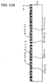
- FIG. 6 is a fragmentary cross sectional elevation view illustrative of multilayer structure of the multilayer interconnection board of the semiconductor device shown in FIG. 4.
- the multilayer interconnection board 3 comprises sequential laminations of multiple interconnection layers, for example, first, second, third, fourth and fifth interconnection layers 5, 6, 7, 8 and 9.
- the second interconnection layer 6 is laminated on the first interconnection layer 5.
- the third interconnection layer 7 is laminated on the second interconnection layer 6.
- the fourth interconnection layer 8 is laminated on the third interconnection layer 7.
- the fifth interconnection layer 9 is laminated on the fourth interconnection layer 8.
- the first interconnection layer 5 is in the second surface side of the multilayer interconnection board 3.
- the solder balls 13 are provided on the first interconnection layer 5.
- the fifth interconnection layer 9 is in the first surface side of the multilayer interconnection board 3.
- the bumps 14 are provided on the fifth interconnection layer 9.
- the first interconnection layer 5 comprises a first level interconnection pattern 5-1, a first level insulating layer 5-2 and a first level contact layer 5-3, wherein the first level interconnection pattern 5-1 is selectively formed in a bottom half region of the first level insulating layer 5-2 and the first level contact layer 5-3 is selectively formed in a top half region of the first level insulating layer 5-2, so that the first level contact layer 5-3 is in contact with a part of the first level interconnection pattern 5-1.
- the second interconnection layer 6 comprises a second level interconnection pattern 6-1, a second level insulating layer 6-2 and a second level contact layer 6-3, wherein the second level interconnection pattern 6-1 is selectively formed in a bottom half region of the second level insulating layer 6-2 and the second level contact layer 6-3 is selectively formed in a top half region of the second level insulating layer 6-2, so that the second level contact layer 6-3 is in contact with a part of the second level interconnection pattern 6-1.
- the second interconnection layer 6 is laminated on the first interconnection layer 5, so that the second level interconnection pattern 6-1 is in contact with the first level contact layer 5-3 of the first interconnection layer 5, whereby the second level interconnection pattern 6-1 is electrically connected through the first level contact layer 5-3 to the first level interconnection pattern 5-1 of the first interconnection layer 5.
- the third interconnection layer 7 comprises a third level interconnection pattern 7-1, a third level insulating layer 7-2 and a third level contact layer 7-3, wherein the third level interconnection pattern 7-1 is selectively formed in a bottom half region of the third level insulating layer 7-2 and the third level contact layer 7-3 is selectively formed in a top half region of the third level insulating layer 7-2, so that the third level contact layer 7-3 is in contact with a part of the third level interconnection pattern 7-1.
- the third interconnection layer 7 is laminated on the second interconnection layer 6, so that the third level interconnection pattern 7-1 is in contact with the second level contact layer 6-3 of the second interconnection layer 6, whereby the third level interconnection pattern 7-1 is electrically connected through the second level contact layer 6-3 to the second level interconnection pattern 6-1 of the second interconnection layer 6.
- the fourth interconnection layer 8 comprises a fourth level interconnection pattern 8-1, a fourth level insulating layer 8-2 and a fourth level contact layer 8-3, wherein the fourth level interconnection pattern 8-1 is selectively formed in a bottom half region of the fourth level insulating layer 8-2 and the fourth level contact layer 8-3 is selectively formed in a top half region of the fourth level insulating layer 8-2, so that the fourth level contact layer 8-3 is in contact with a part of the fourth level interconnection pattern 8-1.
- the fourth interconnection layer 8 is laminated on the third interconnection layer 7, so that the fourth level interconnection pattern 8-1 is in contact with the third level contact layer 7-3 of the third interconnection layer 7, whereby the fourth level interconnection pattern 8-1 is electrically connected through the third level contact layer 7-3 to the third level interconnection pattern 7-1 of the third interconnection layer 7.
- the fifth interconnection layer 9 comprises a fifth level interconnection pattern 9-1 and a fifth level insulating layer 9-2, wherein the fifth level interconnection pattern 9-1 is selectively formed in a bottom half region of the fifth level insulating layer 9-2.
- the fifth interconnection layer 9 is laminated on the fourth interconnection layer 8, so that the fifth level interconnection pattern 9-1 is in contact with the fourth level contact layer 8-3 of the fourth interconnection layer 8, whereby the fifth level interconnection pattern 9-1 is electrically connected through the fourth level contact layer 8-3 to the fourth level interconnection pattern 8-1 of the fourth interconnection layer 8.
- the above first, second third, fourth and fifth level interconnection patterns 5-1, 6-1, 7-1, 8-1 and 9-1 are connected to each other through the first, second, third and fourth level contact layers 5-3, 6-3, 7-3 and 8-3.
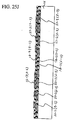
- FIGS. 7A through 7Q arc fragmentary cross sectional elevation views illustrative of a novel method of forming a semiconductor device having a multilayer interconnection board on which a semiconductor chip is mounted in a first embodiment in accordance with the present invention.
- the high rigidity plate 16 may be made of any material having a high rigidity. Metals such as Cu-, Ni-, Al-, W-, Mo-, Au-, Ag- and Pt-based metals, complex materials of different metals and ceramics are available for the high rigidity plate 16.
- an adhesive metal layer of a metal such as a Ti-base alloy, a Cr-base alloy, a Mo-base alloy, and a W-base alloy is formed on a first surface of the high rigidity plate 16 by a sputtering method.
- An electrode material layer of a metal such as Cu, Al, and Ni is then formed on the adhesive metal layer by a sputtering method to form laminations of the adhesive metal layer and the electrode material layer.
- a resist film is then applied on the laminations of the adhesive metal layer and the electrode material layer. The resist film is then patterned by an exposure and a subsequent development to form a resist pattern.
- a selective wet etching process or a selective dry etching process to the laminations of the adhesive metal layer and the electrode material layer is carried out by use of the resist pattern as a mask so as to pattern the laminations of the adhesive metal layer and the electrode material layer, whereby external electrode pads 17-1 are selectively formed on the first surface of the high rigidity plate 16.
- the used resist pattern is then removed.
- a minimum pitch of the external electrode pads 17-1 is not so narrow, then it is possible as a modification that a resist is coated directly on the first surface of the high rigidity plate 16 and then patterned by an exposure and a development to form a resist pattern before a selective electroplating of metal is then carried out by use of the resist pattern as a mask, followed by removal of the used resist pattern.
- an insulative resin thin film 18-1 is then formed over the external electrode pads 17-1 and the first surface of the high rigidity plate 16.
- the insulative resin thin film 18-1 may comprise a polyimide based resin thin film which may be formed by a spin coating method, a chemical vapor deposition method or a physical vapor deposition method.
- silicon dioxide based inorganic materials, and organic materials such as epoxy based resins, silicone based resins, polyolefin based resins, cyanate ester based resins, phenol based resins, naphthalene based resins are available for the insulative resin thin film 18-1. If a fine pattern of not more than 1.0 micrometer is required, it is preferable to use the silicon dioxide based inorganic materials for utilizing diffusion processes of semiconductor.
- the insulative resin thin film 18-1 is selectively removed to form openings 19-1 in the insulative resin thin film 18-1 and over the external electrode pads 17-1.
- a resist film is applied on the insulative resin thin film 18-1 and then patterned by an exposure and a subsequent development to form a resist pattern on the insulative resin thin film 18-1. If the insulative resin thin film 18-1 is made of a material which is removable by a chemical etching process, the insulative resin thin film 18-1 is selectively removed by a wet etching by use of the resist pattern as a mask to form the openings 19-1 in the insulative resin thin film 18-1.
- the insulative resin thin film 18-1 is made of a material which is unremovable by the chemical etching process, the insulative resin thin film 18-1 is selectively removed by a dry etching by use of the resist pattern as a mask to form the openings 19-1 in the insulative resin thin film 18-1.
- the external electrode pads 17-1 are partially shown through the openings 19-1 formed in the insulative resin thin film 18-1. The used resist pattern is then removed.
- an adhesive metal thin film 21a is entirely formed which extends on the surface of the insulative resin thin film 18-1 and the shown parts of the external electrode pads 17-1 by a sputtering method.
- the adhesive metal thin film 21a may be made of a Ti-based alloy, a Cr-based alloy, a Mo-based alloy, or a W-based alloy.
- a metal electrode thin film 21b is also entirely formed on the adhesive metal thin film 21a by a sputtering method, a chemical vapor deposition or an electroless plating method.
- the metal electrode thin film 21b may be made of Cu, Al or Ni. Laminations of the adhesive metal thin film 21a and the metal electrode thin film 21b form a metal thin film 21 which extends on the surface of the insulative resin thin film 18-1 and within the openings 19-1 over the external electrode pads 17-1.
- a resist film is entirely formed on the metal thin film 21 and then patterned by an exposure and a subsequent development to form a resist pattern over the metal thin film 21.
- the metal thin film 21 is then patterned by a wet etching or a dry etching by use of the resist pattern as a mask to form metal thin film contact layers 23-1 in the openings 19-1 and metal thin film interconnection layers 22-1 over the insulative resin thin film 18-1, wherein the metal thin film interconnection layers 22-1 are in contact directly with the metal thin film contact layers 23-1, so that the metal thin film interconnection layers 22-1 are electrically connected through the metal thin film contact layers 23-1 to the external electrode pads 17-1.
- the used resist mask is then removed.
- the insulative resin thin film 18-1 shown in FIG. 7F also corresponds to the first level insulating layer 5-2 of the first interconnection layer 5 shown in FIG. 6.
- the metal thin film contact layers 23-1 shown in FIG. 7F also corresponds to the first level contact layer 5-3 of the first interconnection layer 5.
- the metal thin film interconnection layers 22-1 shown in FIG. 7F also corresponds to the second level interconnection pattern 6-1 of the second interconnection layer 6.
- the resist pattern is formed on the metal thin film 21 so that a selective electroplating of metal such as Cu is carried out by use of the resist pattern as a mask to form Cu-plated patterns over the metal thin film 21.
- the used resist mask is then removed.
- the metal thin film 21 is then selectively etched by use of the Cu-plated patterns as a mask thereby to form the metal thin film interconnection layers 22-1 over the insulative resin thin film 18-1 and the metal thin film contact layers 23-1 in the openings 19-1.
- the thicknesses of the resist film and the metal thin film interconnection layers 22-1 are not more than 1 micrometers.
- an insulative resin thin film 18-2 is then formed over the metal thin film interconnection layers 22-1 and the insulative resin thin film 18-1.
- the insulative resin thin film 18-2 may comprise a polyimide based resin thin film which may be formed by a spin coating method, a chemical vapor deposition method or a physical vapor deposition method.
- silicon dioxide based inorganic materials, and organic materials such as epoxy based resins, silicone based resins, polyolefin based resins, cyanate ester based resins, phenol based resins, naphthalene based resins are available for the insulative resin thin film 18-2.
- the insulative resin thin film 18-2 is selectively removed to form openings 19-2 in the insulative resin thin film 18-2 and over the metal thin film interconnection layers 22-1.
- a resist film is applied on the insulative resin thin film 18-2 and then patterned by an exposure and a subsequent development to form a resist pattern on the insulative resin thin film 18-2.
- the insulative resin thin film 18-2 is made of a material which is removable by a chemical etching process, the insulative resin thin film 18-2 is selectively removed by a wet etching by use of the resist pattern as a mask to form the openings 19-2 in the insulative resin thin film 18-2. If the insulative resin thin film 18-2 is made of a material which is unremovable by the chemical etching process, the insulative resin thin film 18-2 is selectively removed by a dry etching by use of the resist pattern as a mask to form the openings 19-2 in the insulative resin thin film 18-2. The metal thin film interconnection layers 22-1 are partially shown through the openings 19-2 formed in the insulative resin thin film 18-2. The used resist pattern is then removed.
- an adhesive metal thin film is entirely formed which extends on the surface of the insulative resin thin film 18-2 and the shown parts of the metal thin film interconnection layers 22-1 by a sputtering method.
- the adhesive metal thin film may be made of a Ti-based alloy, a Cr-based alloy, a Mo-based alloy, or a W-based alloy.
- a metal electrode thin film is also entirely formed on the adhesive metal thin film by a sputtering method, a chemical vapor deposition or an electroless plating method.
- the metal electrode thin film may be made of Cu, Al or Ni.
- Laminations of the adhesive metal thin film and the metal electrode thin film form a metal thin film which extends on the surface of the insulative resin thin film 18-2 and within the openings 19-2 over the metal thin film interconnection layers 22-1.
- a resist film is entirely formed on the metal thin film and then patterned by an exposure and a subsequent development to form a resist pattern over the metal thin film.
- the metal thin film is then patterned by a wet etching or a dry etching by use of the resist pattern as a mask to form metal thin film contact layers 23-2 in the openings 19-2 and metal thin film interconnection layers 22-2 over the insulative resin thin film 18-2, wherein the metal thin film interconnection layers 22-2 are in contact directly with the metal thin film contact layers 23-2, so that the metal thin film interconnection layers 22-2 are electrically connected through the metal thin film contact layers 23-2 to the metal thin film interconnection layers 22-1.
- the used resist mask is then removed.
- the metal thin film interconnection layers 22-1 shown in FIG. 7H correspond to the second level interconnection pattern 6-1 of the second interconnection layer 6 shown in FIG. 6.
- the metal thin film contact layers 23-2 shown in FIG. 7H also corresponds to the second level contact layer 6-3 of the second interconnection layer 6.
- the metal thin film interconnection layers 22-2 shown in FIG. 7H also corresponds to the third level interconnection pattern 7-1 of the third interconnection layer 7.
- the resist pattern is formed on the metal thin film so that a selective electroplating of metal such as Cu is carried out by use of the resist pattern as a mask to form Cu-plated patterns over the metal thin film.
- the used resist mask is then removed.
- the metal thin film is then selectively etched by use of the Cu-plated patterns as a mask thereby to form the metal thin film interconnection layers 22-2 over the insulative resin thin film 18-2 and the metal thin film contact layers 23-2 in the openings 19-2.
- the thicknesses of the resist film and the metal thin film interconnection layers 22-2 are not more than 1 micrometers.
- an insulative resin thin film 18-3 is then formed over the metal thin film interconnection layers 22-2 and the insulative resin thin film 18-2.
- the insulative resin thin film 18-3 may comprise a polyimide based resin thin film which may be formed by a spin coating method, a chemical vapor deposition method or a physical vapor deposition method.
- silicon dioxide based inorganic materials, and organic materials such as epoxy based resins, silicone based resins, polyolefin based resins, cyanate ester based resins, phenol based resins, naphthalene based resins are available for the insulative resin thin film 18-3.
- the insulative resin thin film 18-3 is selectively removed to form openings 19-3 in the insulative resin thin film 18-3 and over the metal thin film interconnection layers 22-2.
- a resist film is applied on the insulative resin thin film 18-3 and then patterned by an exposure and a subsequent development to form a resist pattern on the insulative resin thin film 18-3.
- the insulative resin thin film 18-3 is made of a material which is removable by a chemical etching process, the insulative resin thin film 18-3 is selectively removed by a wet etching by use of the resist pattern as a mask to form the openings 19-3 in the insulative resin thin film 18-3. If the insulative resin thin film 18-3 is made of a material which is unremovable by the chemical etching process, the insulative resin thin film 18-3 is selectively removed by a dry etching by use of the resist pattern as a mask to form the openings 19-3 in the insulative resin thin film 18-3. The metal thin film interconnection layers 22-2 are partially shown through the openings 19-3 formed in the insulative resin thin film 18-3. The used resist pattern is then removed.
- an adhesive metal thin film is entirely formed which extends on the surface of the insulative resin thin film 18-3 and the shown parts of the metal thin film interconnection layers 22-2 by a sputtering method.
- the adhesive metal thin film may be made of a Ti-based alloy, a Cr-based alloy, a Mo-based alloy, or a W-based alloy.
- a metal electrode thin film is also entirely formed on the adhesive metal thin film by a sputtering method, a chemical vapor deposition or an electroless plating method.
- the metal electrode thin film may be made of Cu, Al or Ni.
- Laminations of the adhesive metal thin film and the metal electrode thin film form a metal thin film which extends on the surface of the insulative resin thin film 18-3 and within the openings 19-3 over the metal thin film interconnection layers 22-2.
- a resist film is entirely formed on the metal thin film and then patterned by an exposure and a subsequent development to form a resist pattern over the metal thin film.
- the metal thin film is then patterned by a wet etching or a dry etching by use of the resist pattern as a mask to form metal thin film contact layers 23-3 in the openings 19-3 and metal thin film interconnection layers 22-3 over the insulative resin thin film 18-3, wherein the metal thin film interconnection layers 22-3 are in contact directly with the metal thin film contact layers 23-3, so that the metal thin film interconnection layers 22-3 are electrically connected through the metal thin film contact layers 23-3 to the metal thin film interconnection layers 22-2.
- the used resist mask is then removed.
- the metal thin film interconnection layers 22-2 shown in FIG. 7J correspond to the third level interconnection pattern 7-1 of the third interconnection layer 7 shown in FIG. 6.
- the metal thin film contact layers 23-3 shown in FIG. 7J also corresponds to the third level contact layer 7-3 of the third interconnection layer 7.
- the metal thin film interconnection layers 22-3 shown in FIG. 7J also corresponds to the fourth level interconnection pattern 8-1 of the third interconnection layer 8.
- the resist pattern is formed on the metal thin film so that a selective electroplating of metal such as Cu is carried out by use of the resist pattern as a mask to form Cu-plated patterns over the metal thin film.
- the used resist mask is then removed.
- the metal thin film is then selectively etched by use of the Cu-plated patterns as a mask thereby to form the metal thin film interconnection layers 22-3 over the insulative resin thin film 18-3 and the metal thin film contact layers 23-3 in the openings 19-3.
- the thicknesses of the resist film and the metal thin film interconnection layers 22-3 are not more than 1 micrometers.
- an insulative resin thin film 18-4 is then formed over the metal thin film interconnection layers 22-3 and the insulative resin thin film 18-3.
- the insulative resin thin film 18-4 may comprise a polyimide based resin thin film which may be formed by a spin coating method, a chemical vapor deposition method or a physical vapor deposition method.
- silicon dioxide based inorganic materials, and organic materials such as epoxy based resins, silicone based resins, polyolefin based resins, cyanate ester based resins, phenol based resins, naphthalene based resins are available for the insulative resin thin film 18-4.
- the insulative resin thin film 18-4 is selectively removed to form openings 19-4 in the insulative resin thin film 18-4 and over the metal thin film interconnection layers 22-3.
- a resist film is applied on the insulative resin thin film 18-4 and then patterned by an exposure and a subsequent development to form a resist pattern on the insulative resin thin film 18-4.
- the insulative resin thin film 18-4 is made of a material which is removable by a chemical etching process, the insulative resin thin film 18-4 is selectively removed by a wet etching by use of the resist pattern as a mask to form the openings 19-4 in the insulative resin thin film 18-4. If the insulative resin thin film 18-4 is made of a material which is unremovable by the chemical etching process, the insulative resin thin film 18-4 is selectively removed by a dry etching by use of the resist pattern as a mask to form the openings 19-4 in the insulative resin thin film 18-3. The metal thin film interconnection layers 22-3 are partially shown through the openings 19-4 formed in the insulative resin thin film 18-4. The used resist pattern is then removed.
- an adhesive metal thin film is entirely formed which extends on the surface of the insulative resin thin film 18-4 and the shown parts of the metal thin film interconnection layers 22-3 by a sputtering method.
- the adhesive metal thin film may be made of a Ti-based alloy, a Cr-based alloy, a Mo-based alloy, or a W-based alloy.
- a metal electrode thin film is also entirely formed on the adhesive metal thin film by a sputtering method, a chemical vapor deposition or an electroless plating method.
- the metal electrode thin film may be made of Cu, Al or Ni.
- Laminations of the adhesive metal thin film and the metal electrode thin film form a metal thin film which extends on the surface of the insulative resin thin film 18-4 and within the openings 19-4 over the metal thin film interconnection layers 22-3.
- a resist film is entirely formed on the metal thin film and then patterned by an exposure and a subsequent development to form a resist pattern over the metal thin film.
- the metal thin film is then patterned by a wet etching or a dry etching by use of the resist pattern as a mask to form metal thin film contact layers 23-4 in the openings 19-4 and pad electrodes 22-4 over the insulative resin thin film 18-4, wherein the pad electrodes 22-4 are in contact directly with the metal thin film contact layers 23-4, so that the pad electrodes 22-4 are electrically connected through the metal thin film contact layers 23-4 to the metal thin film interconnection layers 22-3.
- the used resist mask is then removed.
- the metal thin film interconnection layers 22-3 shown in FIG. 7L correspond to the fourth level interconnection pattern 8-1 of the fourth interconnection layer 8 shown in FIG. 6.
- the pad electrodes 22-4 shown in FIG. 7L also corresponds to the fifth level interconnection pattern 9-1 of the fifth interconnection layer 9.
- the resist pattern is formed on the metal thin film so that a selective electroplating of metal such as Cu is carried out by use of the resist pattern as a mask to form Cu-plated patterns over the metal thin film.
- the used resist mask is then removed.
- the metal thin film is then selectively etched by use of the Cu-plated patterns as a mask thereby to form the pad electrodes 22-4 over the insulative resin thin film 18-4 and the metal thin film contact layers 23-4 in the openings 19-4.
- the thicknesses of the resist film and the pad electrodes 22-4 are not more than 1 micrometers.
- solder resist film 24 is then formed over the pad electrodes 22-4 and the insulative resin thin film 18-4 in order to protect the multilayer interconnection board 3 having the pad electrodes 24.
- the solder resist film 24 shown in FIG. 7M corresponds to the fifth level insulating layer 9-2 of the fifth interconnection layer 9 shown in FIG. 6.
- the solder resist film 24 may comprise an organic insulating film such an epoxy resin film containing an inorganic filler such as fine powders of silicon dioxide.
- the solder resist film 24 may be made of a material which has a large resistivity to external chemical stress, and a large resistivity to a Flux cleaning solution or an Au plating solution as well as a high adhesiveness to a sealing material such as an under-fill material. If the above first to fourth insulative resin thin films 18-1, 18-2, 18-3 and 18-4 are highly resistive to the chemical and chemical stresses, it is possible as a modification to eliminate the formation of the solder resist film 24. The solder resist film 24 is selectively removed to form openings 24a in the solder resist film 24 and over the pad electrodes 22-4.
- solder resist film 24 is made of a non-photosensitive material
- a resist film is applied on the solder resist film 24 and then patterned by an exposure and a subsequent development to form a resist pattern on the solder resist film 24, so that the solder resist film 24 is selectively removed by a wet etching by use of the resist pattern as a mask to form the openings 24a in the solder resist film 24, followed by removal of the used resist pattern.
- the solder resist film 24 is made of a photosensitive material, then the solder resist film 24 is directly patterned by an exposure and a subsequent development to form the openings 24a in the solder resist film 24.
- the electrode pads 22-4 are partially shown through the openings 24a formed in the solder resist film 24.
- the high rigidity plate 16 is completely removed by an etching process, whereby the multilayer interconnection board 3 remains.
- the external electrode pads 17-1 in the first interconnection layer 5 and the pad electrodes 22-4 in the fifth interconnection layer 9 are then subjected to an electroless plating for plating laminated Ni and Au layers or laminated Zn, Ni and Au layers on the external electrode pads 17-1 and the pad electrodes 22-4 in order to improve a bonding property between the external electrode pads 17-1 and also a bonding property between the pad electrodes 22-4 and the bumps 14 of the semiconductor chip 2.
- the multilayer interconnection board 3 is completed, which comprises plural unit multilayer interconnection boards.
- a test for electrical characteristics of the multilayer interconnection board 3 is then made, so that only quality-confirmed units in the plural unit multilayer interconnection boards in the electrical characteristic test are then subjected to a mounting process for mounting semiconductor chips thereon.
- semiconductor chips 2 are mounted on the multilayer interconnection board 3, wherein the semiconductor chips 2 have the plural bumps 14, and the plural bumps 14 are made into contact with the electrode pads 22-4 of the multilayer interconnection board 3, so that the semiconductor chips 2 are electrically connected through the plural bumps 14 to the multilayer interconnection board 3.
- the bumps 14 are made of a metal based solder material such as Sn or Pb
- a flip-chip bonding utilizing a heat re-flow process using Flux is available for bonding the plural bumps 14 to the electrode pads 22-4 of the multilayer interconnection board 3.
- the bumps 14 are made of a metal based solder material such as Au or In
- a flip-chip bonding utilizing a thermo-compression bonding is available for bonding the plural bumps 14 to the electrode pads 22-4 of the multilayer interconnection board 3.
- an insulative resin material 31 is formed which coats side walls of the semiconductor chips 2, an inter-space between the semiconductor chips 2 and the multilayer interconnection board 3 around the bumps 14 and the surface of the solder resist film 24 of the multilayer interconnection board 3 in order to protect the semiconductor chips 2, the bumps 14 and the multilayer interconnection board 3.
- This coating process is carried out by use of a resin injection technique involving a vacuum scaling technique or a transfer sealing technique.
- the insulative resin material 31 may be made of one of epoxy resin materials, silicone resin materials, polyimide resin materials, polyolefin resin materials, cyanate ester resin materials, phenol resin materials and naphthalene resin materials.
- solder balls 13 are formed which are in contact directly with the external electrode pads 17-1 of the multilayer interconnection board 3 to form a semiconductor device 1 having the multilayer interconnection board 3 and the plural semiconductor chips 2 mounted thereon.
- the solder balls 13 serve as external terminals.
- the solder balls 13 may be made of a metal based material such as Sn or Pb.
- the solder balls 13 may also be free of lead.
- the solder balls 13 may be made of an electrically conductive material having a low melting point, a high heat conductivity and a rapid solidity as well as a large surface tension so that the electrically conductive material becomes in the form of balls.
- the semiconductor device 1 is then diced by use of a dicing blade to divide the semiconductor device 1 into plural unit semiconductor devices 32 or flip-chip semiconductor devices 32, each of which comprises the multilayer interconnection board 3 and the single semiconductor chip 2 mounted thereon.
- a heat conductive adhesive layer 41 is provided on a top surface of the semiconductor chip 2.
- a heat spreader 42 is provided on the heat conductive adhesive layer 41 so that the heat spreader 42 is adhered through the heat conductive adhesive layer 41 to the top surface of the semiconductor chip 2.
- a heat generated in the semiconductor chip 2 is conducted through the heat conductive adhesive layer 41 to the heat spreader 42 for causing a heat radiation from the heat spreader 42.
- the heat spreader 42 may be made of a heat conductive material such as a metal base material, for example, Cu, Al, W, Mo, Fe, Ni, and Cr, or Al 2 O 3 , AlN, SiC, other ceramics such as mullite.
- the heat conductive adhesive layer 41 may be made of a resin based material containing a heat conductive material, wherein the resin based material may be one of epoxy resin materials, silicone resin materials, polyimide resin materials, polyolefin resin materials, cyanate ester resin materials, phenol resin materials and naphthalene resin materials, whilst the heat conductive material may be one of Ag, Pd, Cu, Al, Au, Mo, W, diamond, Al 2 O 3 , AlN, and ceramic materials such as mullite, BN and SiC.
- the resin based material may be one of epoxy resin materials, silicone resin materials, polyimide resin materials, polyolefin resin materials, cyanate ester resin materials, phenol resin materials and naphthalene resin materials
- the heat conductive material may be one of Ag, Pd, Cu, Al, Au, Mo, W, diamond, Al 2 O 3 , AlN, and ceramic materials such as mullite, BN and SiC.
- the flip-chip is usually applied to a high speed logic device having a large number of pins, for which reason the heat radiation from the semiconductor chip 2 is important.
- the heat spreader 42 is provided to improve the heat radiation characteristic of the flip-chip semiconductor device 32.
- the base material of the multilayer interconnection board is not largely different in thermal expansion coefficient from the semiconductor chip to reduce a stress applied between the multilayer interconnection board and the semiconductor chip, thereby keeping a high reliability in connection between the multilayer interconnection board and the semiconductor chip.
- the reduction in stress applied between the multilayer interconnection board and the semiconductor chip makes it unnecessary to increase the thicknesses of the multilevel interconnections 17-1, 2-1, 22-2, 22-3 and 24 for stress relaxation, but makes it possible that the thicknesses of the multilevel interconnections 17-1, 2-1, 22-2, 22-3 and 24 are thin, for example, not more than 1 micrometer.
- a metallization technique for the semiconductor wafer and an apparatus therefor are utilized for allowing the resist films and the multilevel interconnections 17-1, 2-1, 22-2, 22-3 and 24 to be patterned finely, thereby permitting a further shrinkage of the interconnection patterns.
- the multilayer interconnection board remains adhered or fixed to the high rigidity plate such as the metal plate during when the multilayer interconnection board is formed, so that the high rigidity plate provides or ensures a high planarity to the multilayer interconnection board.
- the high rigidity plate is different in linear expansion coefficient from the multilayer interconnection board, the high rigidity plate suppresses generation of internal stress in the multilayer interconnection board and expansion of the multilayer interconnection board, so that the high rigidity plate suppresses the multilayer interconnection board from being bent, whereby the multilayer interconnection board is free from any misalignment in patterning the insulating layers and the interconnection layers, resulting in a high yield of the flip-chip semiconductor device.
- the high rigidity plate is necessary or important for keeping the multilayer interconnection board to have the high planarity until the multilayer interconnection board is completed. Notwithstanding, the high rigidity plate is not necessarily needed to the final product, for example, the flip-chip semiconductor device, for which reason as described above, after the multilayer interconnection board has been completed, then the high rigidity plate is removed. After the high rigidity plate is removed from the bottom surface of the multilayer interconnection board, then the bottom surface of the multilayer interconnection board is shown, for which reason the bottom or first insulating layer of the multilayer interconnection board may preferably he made of an insulating material such as an organic material which has a flexibility to an externally applied stress.
- the single multilayer interconnection board is adhered or fixed to the one side of the high rigidity plate to form an asymmetric structure.
- the high rigidity plate prevents the multilayer interconnection board from being bent during the fabrication of the multilayer interconnection board. If the multilayer interconnection boards are adhered or fixed to both surfaces of the high rigidity plate, then it is necessary to form through holes in the high rigidity plate. In accordance with the present invention, however, it is unnecessary to form such the through holes in the high rigidity plate, whereby there are raised no problem with defect of the final product due to dusts generated in forming the through holes in the high rigidity plate nor problem with increase in the manufacturing cost due to additional process for forming the through holes in the high rigidity plate.
- the high rigidity plate is removed after the multilayer interconnection board is completed and before the semiconductor chips are mounted on the multilayer interconnection board.
- the high rigidity plate suppresses various strains of the entire or part of the multilayer interconnection board and the semiconductor chips due to mechanical and thermal stresses applied to the multilayer interconnection board and the semiconductor chips.
- the high rigidity plate suppresses various strains of the entire or part of the multilayer interconnection board and the semiconductor chips due to mechanical and thermal stresses applied to the multilayer interconnection board and the semiconductor chips.
- the above flip-chip semiconductor device 32 is mounted through the solder balls 13 to a circuit board which is not illustrated.
- the solder balls 13 have a small stand-off height which is insufficient for relaxation of the stress applied between the above flip-chip semiconductor device 32 and the circuit board.
- Other novel technique for solving this disadvantage will be described in the following fourth embodiment.
- a second embodiment according to the present invention will be described in detail with reference to the drawings.
- the second embodiment is different from the first embodiment only in the fabrication processes for the flip-chip semiconductor device 32, for which reason the following descriptions will focus on the fabrication processes and the description of the structure of the flip-chip semiconductor device 32 will be omitted.
- FIGS. 8A through 8Q are fragmentary cross sectional elevation views illustrative of a novel method of forming a semiconductor device having a multilayer interconnection board on which a semiconductor chip is mounted in a second embodiment in accordance with the present invention.
- the high rigidity plate 16 may be made of any material having a high rigidity. Metals such as Cu-, Ni-, Al-, W-, Mo-, Au-, Ag- and Pt-based metals, complex materials of different metals and ceramics are available for the high rigidity plate 16.
- an adhesive metal layer of a metal such as a Ti-base alloy, a Cr-base alloy, a Mo-base alloy, and a W-base alloy is formed on a first surface of the high rigidity plate 16 by a sputtering method.
- An electrode material layer of a metal such as Cu, Al, and Ni is then formed on the adhesive metal layer by a sputtering method to form laminations of the adhesive metal layer and the electrode material layer.
- a resist film is then applied on the laminations of the adhesive metal layer and the electrode material layer. The resist film is then patterned by an exposure and a subsequent development to form a resist pattern.
- a selective wet etching process or a selective dry etching process to the laminations of the adhesive metal layer and the electrode material layer is carried out by use of the resist pattern as a mask so as to pattern the laminations of the adhesive metal layer and the electrode material layer, whereby external electrode pads 17-1 are selectively formed on the first surface of the high rigidity plate 16.
- the used resist pattern is then removed.
- a minimum pitch of the external electrode pads 17-1 is not so narrow, then it is possible as a modification that a resist is coated directly on the first surface of the high rigidity plate 16 and then patterned by an exposure and a development to form a resist pattern before a selective electroplating of metal is then carried out by use of the resist pattern as a mask, followed by removal of the used resist pattern.
- an insulative resin thin film 18-1 is then formed over the external electrode pads 17-1 and the first surface of the high rigidity plate 16.
- the insulative resin thin film 18-1 may comprise a polyimide based resin thin film which may be formed by a spin coating method, a chemical vapor deposition method or a physical vapor deposition method.
- silicon dioxide based inorganic materials, and organic materials such as epoxy based resins, silicone based resins, polyolefin based resins, cyanate ester based resins, phenol based resins, naphthalene based resins are available for the insulative resin thin film 18-1. If a fine pattern of not more than 1.0 micrometer is required, it is preferable to use the silicon dioxide based inorganic materials for utilizing diffusion processes of semiconductor.
- the insulative resin thin film 18-1 is selectively removed to form openings 19-1 in the insulative resin thin film 18-1 and over the external electrode pads 17-1.
- a resist film is applied on the insulative resin thin film 18-1 and then patterned by an exposure and a subsequent development to form a resist pattern on the insulative resin thin film 18-1. If the insulative resin thin film 18-1 is made of a material which is removable by a chemical etching process, the insulative resin thin film 18-1 is selectively removed by a wet etching by use of the resist pattern as a mask to form the openings 19-1 in the insulative resin thin film 18-1.
- the insulative resin thin film 18-1 is made of a material which is unremovable by the chemical etching process, the insulative resin thin film 18-1 is selectively removed by a dry etching by use of the resist pattern as a mask to form the openings 19-1 in the insulative resin thin film 18-1.
- the external electrode pads 17-1 are partially shown through the openings 19-1 formed in the insulative resin thin film 18-1. The used resist pattern is then removed.
- an adhesive metal thin film 21a is entirely formed which extends on the surface of the insulative resin thin film 18-1 and the shown parts of the external electrode pads 17-1 by a sputtering method.
- the adhesive metal thin film 21a may be made of a Ti-based alloy, a Cr-based alloy, a Mo-based alloy, or a W-based alloy.
- a metal electrode thin film 21b is also entirely formed on the adhesive metal thin film 21a by a sputtering method, a chemical vapor deposition or an electroless plating method.
- the metal electrode thin film 21b may be made of Cu, Al or Ni. Laminations of the adhesive metal thin film 21a and the metal electrode thin film 21b form a metal thin film 21 which extends on the surface of the insulative resin thin film 18-1 and within the openings 19-1 over the external electrode pads 17-1.
- a resist film is entirely formed on the metal thin film 21 and then patterned by an exposure and a subsequent development to form a resist pattern over the metal thin film 21.
- the metal thin film 21 is then patterned by a wet etching or a dry etching by use of the resist pattern as a mask to form metal thin film contact layers 23-1 in the openings 19-1 and metal thin film interconnection layers 22-1 over the insulative resin thin film 18-1, wherein the metal thin film interconnection layers 22-1 are in contact directly with the metal thin film contact layers 23-1, so that the metal thin film interconnection layers 22-1 are electrically connected through the metal thin film contact layers 23-1 to the external electrode pads 17-1.
- the used resist mask is then removed.
- the insulative resin thin film 18-1 shown in FIG. 8F also corresponds to the first level insulating layer 5-2 of the first interconnection layer 5 shown in FIG. 6.
- the metal thin film contact layers 23-1 shown in FIG. 8F also corresponds to the first level contact layer 5-3 of the first interconnection layer 5.
- the metal thin film interconnection layers 22-1 shown in FIG. 8F also corresponds to the second level interconnection pattern 6-1 of the second interconnection layer 6.
- the resist pattern is formed on the metal thin film 21 so that a selective electroplating of metal such as Cu is carried out by use of the resist pattern as a mask to form Cu-plated patterns over the metal thin film 21.
- the used resist mask is then removed.
- the metal thin film 21 is then selectively etched by use of the Cu-plated patterns as a mask thereby to form the metal thin film interconnection layers 22-1 over the insulative resin thin film 18-1 and the metal thin film contact layers 23-1 in the openings 19-1.
- the thicknesses of the resist film and the metal thin film interconnection layers 22-1 are not more than 1 micrometers.
- an insulative resin thin film 18-2 is then formed over the metal thin film interconnection layers 22-1 and the insulative resin thin film 18-1.
- the insulative resin thin film 18-2 may comprise a polyimide based resin thin film which may be formed by a spin coating method, a chemical vapor deposition method or a physical vapor deposition method.
- silicon dioxide based inorganic materials, and organic materials such as epoxy based resins, silicone based resins, polyolefin based resins, cyanate ester based resins, phenol based resins, naphthalene based resins are available for the insulative resin thin film 18-2.
- the insulative resin thin film 18-2 is selectively removed to form openings 19-2 in the insulative resin thin film 18-2 and over the metal thin film interconnection layers 22-1.
- a resist film is applied on the insulative resin thin film 18-2 and then patterned by an exposure and a subsequent development to form a resist pattern on the insulative resin thin film 18-2.
- the insulative resin thin film 18-2 is made of a material which is removable by a chemical etching process, the insulative resin thin film 18-2 is selectively removed by a wet etching by use of the resist pattern as a mask to form the openings 19-2 in the insulative resin thin film 18-2. If the insulative resin thin film 18-2 is made of a material which is unremovable by the chemical etching process, the insulative resin thin film 18-2 is selectively removed by a dry etching by use of the resist pattern as a mask to form the openings 19-2 in the insulative resin thin film 18-2. The metal thin film interconnection layers 22-1 are partially shown through the openings 19-2 formed in the insulative resin thin film 18-2. The used resist pattern is then removed.
- an adhesive metal thin film is entirely formed which extends on the surface of the insulative resin thin film 18-2 and the shown parts of the metal thin film interconnection layers 22-1 by a sputtering method.
- the adhesive metal thin film may be made of a Ti-based alloy, a Cr-based alloy, a Mo-based alloy, or a W-based alloy.
- a metal electrode thin film is also entirely formed on the adhesive metal thin film by a sputtering method, a chemical vapor deposition or an electroless plating method.
- the metal electrode thin film may be made of Cu, Al or Ni.
- Laminations of the adhesive metal thin film and the metal electrode thin film form a metal thin film which extends on the surface of the insulative resin thin film 18-2 and within the openings 19-2 over the metal thin film interconnection layers 22-1.
- a resist film is entirely formed on the metal thin film and then patterned by an exposure and a subsequent development to form a resist pattern over the metal thin film.
- the metal thin film is then patterned by a wet etching or a dry etching by use of the resist pattern as a mask to form metal thin film contact layers 23-2 in the openings 19-2 and metal thin film interconnection layers 22-2 over the insulative resin thin film 18-2, wherein the metal thin film interconnection layers 22-2 are in contact directly with the metal thin film contact layers 23-2, so that the metal thin film interconnection layers 22-2 are electrically connected through the metal thin film contact layers 23-2 to the metal thin film interconnection layers 22-1.
- the used resist mask is then removed.
- the metal thin film interconnection layers 22-1 shown in FIG. 8H correspond to the second level interconnection pattern 6-1 of the second interconnection layer 6 shown in FIG. 6.
- the metal thin film contact layers 23-2 shown in FIG. 8H also corresponds to the second level contact layer 6-3 of the second interconnection layer 6.
- the metal thin film interconnection layers 22-2 shown in FIG. 8H also corresponds to the third level interconnection pattern 7-1 of the third interconnection layer 7.
- the resist pattern is formed on the metal thin film so that a selective electroplating of metal such as Cu is carried out by use of the resist pattern as a mask to form Cu-plated patterns over the metal thin film.
- the used resist mask is then removed.
- the metal thin film is then selectively etched by use of the Cu-plated patterns as a mask thereby to form the metal thin film interconnection layers 22-2 over the insulative resin thin film 18-2 and the metal thin film contact layers 23-2 in the openings 19-2.
- the thicknesses of the resist film and the metal thin film interconnection layers 22-2 are not more than 1 micrometers.
- an insulative resin thin film 18-3 is then formed over the metal thin film interconnection layers 22-2 and the insulative resin thin film 18-2.
- the insulative resin thin film 18-3 may comprise a polyimide based resin thin film which may be formed by a spin coating method, a chemical vapor deposition method or a physical vapor deposition method.
- silicon dioxide based inorganic materials, and organic materials such as epoxy based resins, silicone based resins, polyolefin based resins, cyanate ester based resins, phenol based resins, naphthalene based resins are available for the insulative resin thin film 18-3.
- the insulative resin thin film 18-3 is selectively removed to form openings 19-3 in the insulative resin thin film 18-3 and over the metal thin film interconnection layers 22-2.
- a resist film is applied on the insulative resin thin film 18-3 and then patterned by an exposure and a subsequent development to form a resist pattern on the insulative resin thin film 18-3.
- the insulative resin thin film 18-3 is made of a material which is removable by a chemical etching process, the insulative resin thin film 18-3 is selectively removed by a wet etching by use of the resist pattern as a mask to form the openings 19-3 in the insulative resin thin film 18-3. If the insulative resin thin film 18-3 is made of a material which is unremovable by the chemical etching process, the insulative resin thin film 18-3 is selectively removed by a dry etching by use of the resist pattern as a mask to form the openings 19-3 in the insulative resin thin film 18-3. The metal thin film interconnection layers 22-2 are partially shown through the openings 19-3 formed in the insulative resin thin film 18-3. The used resist pattern is then removed.
- an adhesive metal thin film is entirely formed which extends on the surface of the insulative resin thin film 18-3 and the shown parts of the metal thin film interconnection layers 22-2 by a sputtering method.
- the adhesive metal thin film may be made of a Ti-based alloy, a Cr-based alloy, a Mo-based alloy, or a W-based alloy.
- a metal electrode thin film is also entirely formed on the adhesive metal thin film by a sputtering method, a chemical vapor deposition or an electroless plating method.
- the metal electrode thin film may be made of Cu, Al or Ni.
- Laminations of the adhesive metal thin film and the metal electrode thin film form a metal thin film which extends on the surface of the insulative resin thin film 18-3 and within the openings 19-3 over the metal thin film interconnection layers 22-2.
- a resist film is entirely formed on the metal thin film and then patterned by an exposure and a subsequent development to form a resist pattern over the metal thin film.
- the metal thin film is then patterned by a wet etching or a dry etching by use of the resist pattern as a mask to form metal thin film contact layers 23-3 in the openings 19-3 and metal thin film interconnection layers 22-3 over the insulative resin thin film 18-3, wherein the metal thin film interconnection layers 22-3 are in contact directly with the metal thin film contact layers 23-3, so that the metal thin film interconnection layers 22-3 are electrically connected through the metal thin film contact layers 23-3 to the metal thin film interconnection layers 22-2.
- the used resist mask is then removed.
- the metal thin film interconnection layers 22-2 shown in FIG. 8J correspond to the third level interconnection pattern 7-1 of the third interconnection layer 7 shown in FIG. 6.
- the metal thin film contact layers 23-3 shown in FIG. 8J also corresponds to the third level contact layer 7-3 of the third interconnection layer 7.
- the metal thin film interconnection layers 22-3 shown in FIG. 8J also corresponds to the fourth level interconnection pattern 8-1 of the third interconnection layer 8.
- the resist pattern is formed on the metal thin film so that a selective electroplating of metal such as Cu is carried out by use of the resist pattern as a mask to form Cu-plated patterns over the metal thin film.
- the used resist mask is then removed.
- the metal thin film is then selectively etched by use of the Cu-plated patterns as a mask thereby to form the metal thin film interconnection layers 22-3 over the insulative resin thin film 18-3 and the metal thin film contact layers 23-3 in the openings 19-3.
- the thicknesses of the resist film and the metal thin film interconnection layers 22-3 are not more than 1 micrometers.
- an insulative resin thin film 18-4 is then formed over the metal thin film interconnection layers 22-3 and the insulative resin thin film 18-3.
- the insulative resin thin film 18-4 may comprise a polyimide based resin thin film which may be formed by a spin coating method, a chemical vapor deposition method or a physical vapor deposition method.
- silicon dioxide based inorganic materials, and organic materials such as epoxy based resins, silicone based resins, polyolefin based resins, cyanate ester based resins, phenol based resins, naphthalene based resins are available for the insulative resin thin film 18-4.
- the insulative resin thin film 18-4 is selectively removed to form openings 19-4 in the insulative resin thin film 18-4 and over the metal thin film interconnection layers 22-3.
- a resist film is applied on the insulative resin thin film 18-4 and then patterned by an exposure and a subsequent development to form a resist pattern on the insulative resin thin film 18-4.
- the insulative resin thin film 18-4 is made of a material which is removable by a chemical etching process, the insulative resin thin film 18-4 is selectively removed by a wet etching by use of the resist pattern as a mask to form the openings 19-4 in the insulative resin thin film 18-4. If the insulative resin thin film 18-4 is made of a material which is unremovable by the chemical etching process, the insulative resin thin film 18-4 is selectively removed by a dry etching by use of the resist pattern as a mask to form the openings 19-4 in the insulative resin thin film 18-3. The metal thin film interconnection layers 22-3 are partially shown through the openings 19-4 formed in the insulative resin thin film 18-4. The used resist pattern is then removed.
- an adhesive metal thin film is entirely formed which extends on the surface of the insulative resin thin film 18-4 and the shown parts of the metal thin film interconnection layers 22-3 by a sputtering method.
- the adhesive metal thin film may be made of a Ti-based alloy, a Cr-based alloy, a Mo-based alloy, or a W-based alloy.
- a metal electrode thin film is also entirely formed on the adhesive metal thin film by a sputtering method, a chemical vapor deposition or an electroless plating method.
- the metal electrode thin film may be made of Cu, Al or Ni.
- Laminations of the adhesive metal thin film and the metal electrode thin film form a metal thin film which extends on the surface of the insulative resin thin film 18-4 and within the openings 19-4 over the metal thin film interconnection layers 22-3.
- a resist film is entirely formed on the metal thin film and then patterned by an exposure and a subsequent development to form a resist pattern over the metal thin film.
- the metal thin film is then patterned by a wet etching or a dry etching by use of the resist pattern as a mask to form metal thin film contact layers 23-4 in the openings 19-4 and pad electrodes 22-4 over the insulative resin thin film 18-4, wherein the pad electrodes 22-4 are in contact directly with the metal thin film contact layers 23-4, so that the pad electrodes 22-4 are electrically connected through the metal thin film contact layers 23-4 to the metal thin film interconnection layers 22-3.
- the used resist mask is then removed.
- the metal thin film interconnection layers 22-3 shown in FIG. 8L correspond to the fourth level interconnection pattern 8-1 of the fourth interconnection layer 8 shown in FIG. 6.
- the metal thin film contact layers 23-4 shown in FIG. 8L also corresponds to the fourth level contact layer 8-3 of the fourth interconnection layer 8.
- the pad electrodes 22-4 shown in FIG. 8L also corresponds to the fifth level interconnection pattern 9-1 of the fifth interconnection layer 9.
- the resist pattern is formed on the metal thin film so that a selective electroplating of metal such as Cu is carried out by use of the resist pattern as a mask to form Cu-plated patterns over the metal thin film.
- the used resist mask is then removed.
- the metal thin film is then selectively etched by use of the Cu-plated patterns as a mask thereby to form the pad electrodes 22-4 over the insulative resin thin film 18-4 and the metal thin film contact layers 23-4 in the openings 19-4.
- the thicknesses of the resist film and the pad electrodes 22-4 are not more than 1 micrometers.
- solder resist film 24 is then formed over the pad electrodes 22-4 and the insulative resin thin film 18-4 in order to protect the multilayer interconnection board 3 having the pad electrodes 24.
- the solder resist film 24 shown in FIG. 8M corresponds to the fifth level insulating layer 9-2 of the fifth interconnection layer 9 shown in FIG. 6.
- the solder resist film 24 may comprise an organic insulating film such an epoxy resin film containing an inorganic filler such as fine powders of silicon dioxide.
- the solder resist film 24 may be made of a material which has a large resistivity to external chemical stress, and a large resistivity to a Flux cleaning solution or an Au plating solution as well as a high adhesiveness to a sealing material such as an under-fill material. If the above first to fourth insulative resin thin films 18-1, 18-2, 18-3 and 18-4 are highly resistive to the chemical and chemical stresses, it is possible as a modification to eliminate the formation of the solder resist film 24. The solder resist film 24 is selectively removed to form openings 24a in the solder resist film 24 and over the pad electrodes 22-4.
- solder resist film 24 is made of a non-photosensitive material
- a resist film is applied on the solder resist film 24 and then patterned by an exposure and a subsequent development to form a resist pattern on the solder resist film 24, so that the solder resist film 24 is selectively removed by a wet etching by use of the resist pattern as a mask to form the openings 24a in the solder resist film 24, followed by removal of the used resist pattern.
- the solder resist film 24 is made of a photosensitive material, then the solder resist film 24 is directly patterned by an exposure and a subsequent development to form the openings 24a in the solder resist film 24.
- the electrode pads 22-4 are partially shown through the openings 24a formed in the solder resist film 24.
- semiconductor chips 2 are mounted on the multilayer interconnection board 3, wherein the semiconductor chips 2 have the plural bumps 14, and the plural bumps 14 are made into contact with the electrode pads 22-4 of the multilayer interconnection board 3, so that the semiconductor chips 2 are electrically connected through the plural bumps 14 to the multilayer interconnection board 3.
- the bumps 14 are made of a metal based solder material such as Sn or Pb
- a flip-chip bonding utilizing a heat re-flow process using Flux is available for bonding the plural bumps 14 to the electrode pads 22-4 of the multilayer interconnection board 3.
- the bumps 14 are made of a metal based solder material such as Au or In
- a flip-chip bonding utilizing a thermo-compression bonding is available for bonding the plural bumps 14 to the electrode pads 22-4 of the multilayer interconnection board 3.
- the high rigidity plate 16 is completely removed by an etching process, whereby the multilayer interconnection board 3 remains.
- the external electrode pads 17-1 in the first interconnection layer 5 and the pad electrodes 22-4 in the fifth interconnection layer 9 are then subjected to an electroless plating for plating laminated Ni and Au layers or laminated Zn, Ni and Au layers on the external electrode pads 17-1 and the pad electrodes 22-4 in order to improve a bonding property between the external electrode pads 17-1 and also a bonding property between the pad electrodes 22-4 and the bumps 14 of the semiconductor chip 2.
- the multilayer interconnection board 3 is completed, which comprises plural unit multilayer interconnection boards.
- an insulative resin material 31 is formed which coats side walls of the semiconductor chips 2, an inter-space between the semiconductor chips 2 and the multilayer interconnection board 3 around the bumps 14 and the surface of the solder resist film 24 of the multilayer interconnection board 3 in order to protect the semiconductor chips 2, the bumps 14 and the multilayer interconnection board 3.
- This coating process is carried out by use of a resin injection technique involving a vacuum sealing technique or a transfer sealing technique.
- the insulative resin material 31 may be made of one of epoxy resin materials, silicone resin materials, polyimide resin materials, polyolefin resin materials, cyanate ester resin materials, phenol resin materials and naphthalene resin materials.
- solder balls 13 are formed which are in contact directly with the external electrode pads 17-1 of the multilayer interconnection board 3 to form a semiconductor device 1 having the multilayer interconnection board 3 and the plural semiconductor chips 2 mounted thereon.
- the solder balls 13 serve as external terminals.
- the solder balls 13 may be made of a metal based material such as Sn or Pb.
- the solder balls 13 may also be free of lead.
- the solder balls 13 may be made of an electrically conductive material having a low melting point, a high heat conductivity and a rapid solidity as well as a large surface tension so that the electrically conductive material becomes in the form of balls.
- the semiconductor device 1 is then diced by use of a dicing blade to divide the semiconductor device 1 into plural unit semiconductor devices 32 or flip-chip semiconductor devices 32, each of which comprises the multilayer interconnection board 3 and the single semiconductor chip 2 mounted thereon.
- a heat conductive adhesive layer 41 is provided on a top surface of the semiconductor chip 2.
- a heat spreader 42 is provided on the heat conductive adhesive layer 41 so that the heat spreader 42 is adhered through the heat conductive adhesive layer 41 to the top surface of the semiconductor chip 2.
- a heat generated in the semiconductor chip 2 is conducted through the heat conductive adhesive layer 41 to the heat spreader 42 for causing a heat radiation from the heat spreader 42.
- the heat spreader 42 may be made of a heat conductive material such as a metal base material, for example, Cu, Al, W, Mo, Fe, Ni, and Cr, or Al 2 O 3 , AlN, SiC, other ceramics such as mullite.
- the heat conductive adhesive layer 41 may be made of a resin based material containing a heat conductive material, wherein the resin based material may be one of epoxy resin materials, silicone resin materials, polyimide resin materials, polyolefin resin materials, cyanate ester resin materials, phenol resin materials and naphthalene resin materials, whilst the heat conductive material may be one of Ag, Pd, Cu, Al, Au, Mo, W, diamond, Al 2 O 3 , AlN, and ceramic materials such as mullite, BN and SiC.
- the resin based material may be one of epoxy resin materials, silicone resin materials, polyimide resin materials, polyolefin resin materials, cyanate ester resin materials, phenol resin materials and naphthalene resin materials
- the heat conductive material may be one of Ag, Pd, Cu, Al, Au, Mo, W, diamond, Al 2 O 3 , AlN, and ceramic materials such as mullite, BN and SiC.
- the flip-chip is usually applied to a high speed logic device having a large number of pins, for which reason the heat radiation from the semiconductor chip 2 is important.
- the heat spreader 42 is provided to improve the heat radiation characteristic of the flip-chip semiconductor device 32.
- the base material of the multilayer interconnection board is not largely different in thermal expansion coefficient from the semiconductor chip to reduce a stress applied between the multilayer interconnection board and the semiconductor chip, thereby keeping a high reliability in connection between the multilayer interconnection board and the semiconductor chip.
- the reduction in stress applied between the multilayer interconnection board and the semiconductor chip makes it unnecessary to increase the thicknesses of the multilevel interconnections 17-1, 2-1, 22-2, 22-3 and 24 for stress relaxation, but makes it possible that the thicknesses of the multilevel interconnections 17-1, 2-1, 22-2, 22-3 and 24 are thin, for example, not more than 1 micrometer.
- a metallization technique for the semiconductor wafer and an apparatus therefor are utilized for allowing the resist films and the multilevel interconnections 17-1, 2-1, 22-2, 22-3 and 24 to be patterned finely, thereby permitting a further shrinkage of the interconnection patterns.
- the multilayer interconnection board remains adhered or fixed to the high rigidity plate such as the metal plate during when the multilayer interconnection board is formed, so that the high rigidity plate provides or ensures a high planarity to the multilayer interconnection board.
- the high rigidity plate is different in linear expansion coefficient from the multilayer interconnection board, the high rigidity plate suppresses generation of internal stress in the multilayer interconnection board and expansion of the multilayer interconnection board, so that the high rigidity plate suppresses the multilayer interconnection board from being bent, whereby the multilayer interconnection board is free from any misalignment in patterning the insulating layers and the interconnection layers, resulting in a high yield of the flip-chip semiconductor device.
- the high rigidity plate is necessary or important for keeping the multilayer interconnection board to have the high planarity until the multilayer interconnection board is completed. Notwithstanding, the high rigidity plate is not necessarily needed to the final product, for example, the flip-chip semiconductor device, for which reason as described above, after the multilayer interconnection board has been completed, then the high rigidity plate is removed. After the high rigidity plate is removed from the bottom surface of the multilayer interconnection board, then the bottom surface of the multilayer interconnection board is shown, for which reason the bottom or first insulating layer of the multilayer interconnection board may preferably be made of an insulating material such as an organic material which has a flexibility to an externally applied stress.
- the single multilayer interconnection board is adhered or fixed to the one side of the high rigidity plate to form an asymmetric structure.
- the high rigidity plate prevents the multilayer interconnection board from being bent during the fabrication of the multilayer interconnection board. If the multilayer interconnection boards are adhered or fixed to both surfaces of the high rigidity plate, then it is necessary to form through holes in the high rigidity plate. In accordance with the present invention, however, it is unnecessary to form such the through holes in the high rigidity plate, whereby there are raised no problem with defect of the final product due to dusts generated in forming the through holes in the high rigidity plate nor problem with increase in the manufacturing cost due to additional process for forming the through holes in the high rigidity plate.
- the high rigidity plate is removed from the multilayer interconnection board after the semiconductor chips have been mounted on the multilayer interconnection board.
- the multilayer interconnection board still remains adhered or fixed to the high rigidity plate, so that in order to ensure or keep the high planarity of the multilayer interconnection board, the high rigidity plate suppresses various strains of the entire or part of the multilayer interconnection board and the semiconductor chips due to mechanical and thermal stresses applied to the multilayer interconnection board and the semiconductor chips.
- a third embodiment according to the present invention will be described in detail with reference to the drawings.
- the third embodiment is different from the first embodiment only in the fabrication processes for the flip-chip semiconductor device 32, for which reason the following descriptions will focus on the fabrication processes and the description of the structure of the flip-chip semiconductor device 32 will be omitted.
- FIGS. 9A through 9P are fragmentary cross sectional elevation views illustrative of a novel method of forming a semiconductor device having a multilayer interconnection board on which a semiconductor chip is mounted in a third embodiment in accordance with the present invention.
- the high rigidity plate 16 may be made of any material having a high rigidity. Metals such as Cu-, Ni-, Al-, W-, Mo-, Au-, Ag- and Pt-based metals, complex materials of different metals and ceramics are available for the high rigidity plate 16.
- an adhesive metal layer of a metal such as a Ti-base alloy, a Cr-base alloy, a Mo-base alloy, and a W-base alloy is formed on a first surface of the high rigidity plate 16 by a sputtering method.
- An electrode material layer of a metal such as Cu, Al, and Ni is then formed on the adhesive metal layer by a sputtering method to form laminations of the adhesive metal layer and the electrode material layer.
- a resist film is then applied on the laminations of the adhesive metal layer and the electrode material layer. The resist film is then patterned by an exposure and a subsequent development to form a resist pattern.
- a selective wet etching process or a selective dry etching process to the laminations of the adhesive metal layer and the electrode material layer is carried out by use of the resist pattern as a mask so as to pattern the laminations of the adhesive metal layer and the electrode material layer, whereby external electrode pads 17-1 are selectively formed on the first surface of the high rigidity plate 16.
- the used resist pattern is then removed.
- a minimum pitch of the external electrode pads 17-1 is not so narrow, then it is possible as a modification that a resist is coated directly on the first surface of the high rigidity plate 16 and then patterned by an exposure and a development to form a resist pattern before a selective electroplating of metal is then carried out by use of the resist pattern as a mask, followed by removal of the used resist pattern.
- an insulative resin thin film 18-1 is then formed over the external electrode pads 17-1 and the first surface of the high rigidity plate 16.
- the insulative resin thin film 18-1 may comprise a polyimide based resin thin film which may be formed by a spin coating method, a chemical vapor deposition method or a physical vapor deposition method.
- silicon dioxide based inorganic materials, and organic materials such as epoxy based resins, silicone based resins, polyolefin based resins, cyanate ester based resins, phenol based resins, naphthalene based resins are available for the insulative resin thin film 18-1. If a fine pattern of not more than 1.0 micrometer is required, it is preferable to use the silicon dioxide based inorganic materials for utilizing diffusion processes of semiconductor.
- the insulative rosin thin film 18-1 is selectively removed to form openings 19-1 in the insulative resin thin film 18-1 and over the external electrode pads 17-1.
- a resist film is applied on the insulative resin thin film 18-1 and then patterned by an exposure and a subsequent development to form a resist pattern on the insulative resin thin film 18-1. If the insulative resin thin film 18-1 is made of a material which is removable by a chemical etching process, the insulative resin thin film 18-1 is selectively removed by a wet etching by use of the resist pattern as a mask to form the openings 19-1 in the insulative resin thin film 18-1.
- the insulative resin thin film 18-1 is made of a material which is unremovable by the chemical etching process, the insulative resin thin film 18-1 is selectively removed by a dry etching by use of the resist pattern as a mask to form the openings 19-1 in the insulative resin thin film 18-1.
- the external electrode pads 17-1 are partially shown through the openings 19-1 formed in the insulative resin thin film 18-1. The used resist pattern is then removed.
- an adhesive metal thin film 21a is entirely formed which extends on the surface of the insulative resin thin film 18-1 and the shown parts of the external electrode pads 17-1 by a sputtering method.
- the adhesive metal thin film 21a may be made of a Ti-based alloy, a Cr-based alloy, a Mo-based alloy, or a W-based alloy.
- a metal electrode thin film 21b is also entirely formed on the adhesive metal thin film 21a by a sputtering method, a chemical vapor deposition or an electroless plating method.
- the metal electrode thin film 21b may he made of Cu, Al or Ni. Laminations of the adhesive metal thin film 21a and the metal electrode thin film 21b form a metal thin film 21 which extends on the surface of the insulative resin thin film 18-1 and within the openings 19-1 over the external electrode pads 17-1.
- a resist film is entirely formed on the metal thin film 21 and then patterned by an exposure and a subsequent development to form a resist pattern over the metal thin film 21.
- the metal thin film 21 is then patterned by a wet etching or a dry etching by use of the resist pattern as a mask to form metal thin film contact layers 23-1 in the openings 19-1 and metal thin film interconnection layers 22-1 over the insulative resin thin film 18-1, wherein the metal thin film interconnection layers 22-1 are in contact directly with the metal thin film contact layers 23-1, so that the metal thin film interconnection layers 22-1 are electrically connected through the metal thin film contact layers 23-1 to the external electrode pads 17-1.
- the used resist mask is then removed.
- the insulative resin thin film 18-1 shown in FIG. 9F also corresponds to the first level insulating layer 5-2 of the first interconnection layer 5 shown in FIG. 6.
- the metal thin film contact layers 23-1 shown in FIG. 9F also corresponds to the first level contact layer 5-3 of the first interconnection layer 5.
- the metal thin film interconnection layers 22-1 shown in FIG. 9F also corresponds to the second level interconnection pattern 6-1 of the second interconnection layer 6.
- the resist pattern is formed on the metal thin film 21 so that a selective electroplating of metal such as Cu is carried out by use of the resist pattern as a mask to form Cu-plated patterns over the metal thin film 21.
- the used resist mask is then removed.
- the metal thin film 21 is then selectively etched by use of the Cu-plated patterns as a mask thereby to form the metal thin film interconnection layers 22-1 over the insulative resin thin film 18-1 and the metal thin film contact layers 23-1 in the openings 19-1.
- the thicknesses of the resist film and the metal thin film interconnection layers 22-1 are not more than 1 micrometers.
- an insulative resin thin film 18-2 is then formed over the metal thin film interconnection layers 22-1 and the insulative resin thin film 18-1.
- the insulative resin thin film 18-2 may comprise a polyimide based resin thin film which may be formed by a spin coating method, a chemical vapor deposition method or a physical vapor deposition method.
- silicon dioxide based inorganic materials, and organic materials such as epoxy based resins, silicone based resins, polyolefin based resins, cyanate ester based resins, phenol based resins, naphthalene based resins are available for the insulative resin thin film 18-2.
- the insulative resin thin film 18-2 is selectively removed to form openings 19-2 in the insulative resin thin film 18-2 and over the metal thin film interconnection layers 22-1.
- a resist film is applied on the insulative resin thin film 18-2 and then patterned by an exposure and a subsequent development to form a resist pattern on the insulative resin thin film 18-2.
- the insulative resin thin film 18-2 is made of a material which is removable by a chemical etching process, the insulative resin thin film 18-2 is selectively removed by a wet etching by use of the resist pattern as a mask to form the openings 19-2 in the insulative resin thin film 18-2. If the insulative resin thin film 18-2 is made of a material which is unremovable by the chemical etching process, the insulative resin thin film 18-2 is selectively removed by a dry etching by use of the resist pattern as a mask to form the openings 19-2 in the insulative resin thin film 18-2. The metal thin film interconnection layers 22-1 are partially shown through the openings 19-2 formed in the insulative resin thin film 18-2. The used resist pattern is then removed.
- an adhesive metal thin film is entirely formed which extends on the surface of the insulative resin thin film 18-2 and the shown parts of the metal thin film interconnection layers 22-1 by a sputtering method.
- the adhesive metal thin film may be made of a Ti-based alloy, a Cr-based alloy, a Mo-based alloy, or a W-based alloy.
- a metal electrode thin film is also entirely formed on the adhesive metal thin film by a sputtering method, a chemical vapor deposition or an electroless plating method.
- the metal electrode thin film may be made of Cu, Al or Ni.
- Laminations of the adhesive metal thin film and the metal electrode thin film form a metal thin film which extends on the surface of the insulative resin thin film 18-2 and within the openings 19-2 over the metal thin film interconnection layers 22-1.
- a resist film is entirely formed on the metal thin film and then patterned by an exposure and a subsequent development to form a resist pattern over the metal thin film.
- the metal thin film is then patterned by a wet etching or a dry etching by use of the resist pattern as a mask to form metal thin film contact layers 23-2 in the openings 19-2 and metal thin film interconnection layers 22-2 over the insulative resin thin film 18-2, wherein the metal thin film interconnection layers 22-2 are in contact directly with the metal thin film contact layers 23-2, so that the metal thin film interconnection layers 22-2 are electrically connected through the metal thin film contact layers 23-2 to the metal thin film interconnection layers 22-1.
- the used resist mask is then removed.
- the metal thin film interconnection layers 22-1 shown in FIG. 9H correspond to the second level interconnection pattern 6-1 of the second interconnection layer 6 shown in FIG. 6.
- the metal thin film contact layers 23-2 shown in FIG. 9H also corresponds to the second level contact layer 6-3 of the second interconnection layer 6.
- the metal thin film interconnection layers 22-2 shown in FIG. 9H also corresponds to the third level interconnection pattern 7-1 of the third interconnection layer 7.
- the resist pattern is formed on the metal thin film so that a selective electroplating of metal such as Cu is carried out by use of the resist pattern as a mask to form Cu-plated patterns over the metal thin film.
- the used resist mask is then removed.
- the metal thin film is then selectively etched by use of the Cu-plated patterns as a mask thereby to form the metal thin film interconnection layers 22-2 over the insulative resin thin film 18-2 and the metal thin film contact layers 23-2 in the openings 19-2.
- the thicknesses of the resist film and the metal thin film interconnection layers 22-2 are not more than 1 micrometers.
- an insulative resin thin film 18-3 is then formed over the metal thin film interconnection layers 22-2 and the insulative resin thin film 18-2.
- the insulative resin thin film 18-3 may comprise a polyimide based resin thin film which may be formed by a spin coating method, a chemical vapor deposition method or a physical vapor deposition method.
- silicon dioxide based inorganic materials, and organic materials such as epoxy based resins, silicone based resins, polyolefin based resins, cyanate ester based resins, phenol based resins, naphthalene based resins are available for the insulative resin thin film 18-3.
- the insulative resin thin film 18-3 is selectively removed to form openings 19-3 in the insulative resin thin film 18-3 and over the metal thin film interconnection layers 22-2.
- a resist film is applied on the insulative resin thin film 18-3 and then patterned by an exposure and a subsequent development to form a resist pattern on the insulative resin thin film 18-3.
- the insulative resin thin film 18-3 is made of a material which is removable by a chemical etching process, the insulative resin thin film 18-3 is selectively removed by a wet etching by use of the resist pattern as a mask to form the openings 19-3 in the insulative resin thin film 18-3. If the insulative resin thin film 18-3 is made of a material which is unremovable by the chemical etching process, the insulative resin thin film 18-3 is selectively removed by a dry etching by use of the resist pattern as a mask to form the openings 19-3 in the insulative resin thin film 18-3. The metal thin film interconnection layers 22-2 are partially shown through the openings 19-3 formed in the insulative resin thin film 18-3, The used resist pattern is then removed.
- an adhesive metal thin film is entirely formed which extends on the surface of the insulative resin thin film 18-3 and the shown parts of the metal thin film interconnection layers 22-2 by a sputtering method.
- the adhesive metal thin film may be made of a Ti-based alloy, a Cr-based alloy, a Mo-based alloy, or a W-based alloy.
- a metal electrode thin film is also entirely formed on the adhesive metal thin film by a sputtering method, a chemical vapor deposition or an electroless plating method.
- the metal electrode thin film may be made of Cu, Al or Ni.
- Laminations of the adhesive metal thin film and the metal electrode thin film form a metal thin film which extends on the surface of the insulative resin thin film 18-3 and within the openings 19-3 over the metal thin film interconnection layers 22-2.
- a resist film is entirely formed on the metal thin film and then patterned by an exposure and a subsequent development to form a resist pattern over the metal thin film.
- the metal thin film is then patterned by a wet etching or a dry etching by use of the resist pattern as a mask to form metal thin film contact layers 23-3 in the openings 19-3 and metal thin film interconnection layers 22-3 over the insulative resin thin film 18-3, wherein the metal thin film interconnection layers 22-3 are in contact directly with the metal thin film contact layers 23-3, so that the metal thin film interconnection layers 22-3 are electrically connected through the metal thin film contact layers 23-3 to the metal thin film interconnection layers 22-2.
- the used resist mask is then removed.
- the metal thin film interconnection layers 22-2 shown in FIG. 9J correspond to the third level interconnection pattern 7-1 of the third interconnection layer 7 shown in FIG. 6.
- the metal thin film contact layers 23-3 shown in FIG. 9J also corresponds to the third level contact layer 7-3 of the third interconnection layer 7.
- the metal thin film interconnection layers 22-3 shown in FIG. 9J also corresponds to the fourth level interconnection pattern 8-1 of the third interconnection layer 8.
- the resist pattern is formed on the metal thin film so that a selective electroplating of metal such as Cu is carried out by use of the resist pattern as a mask to form Cu-plated patterns over the metal thin film.
- the used resist mask is then removed.
- the metal thin film is then selectively etched by use of the Cu-plated patterns as a mask thereby to form the metal thin film interconnection layers 22-3 over the insulative resin thin film 18-3 and the metal thin film contact layers 23-3 in the openings 19-3.
- the thicknesses of the resist film and the metal thin film interconnection layers 22-3 are not more than 1 micrometers.
- an insulative resin thin film 18-4 is then formed over the metal thin film interconnection layers 22-3 and the insulative resin thin film 18-3.
- the insulative rosin thin film 18-4 may comprise a polyimide based resin thin film which may be formed by a spin coating method, a chemical vapor deposition method or a physical vapor deposition method.
- silicon dioxide based inorganic materials, and organic materials such as epoxy based resins, silicone based resins, polyolefin based resins, cyanate ester based resins, phenol based resins, naphthalene based resins are available for the insulative resin thin film 18-4.
- the insulative resin thin film 18-4 is selectively removed to form openings 19-4 in the insulative resin thin film 18-4 and over the metal thin film interconnection layers 22-3.
- a resist film is applied on the insulative resin thin film 18-4 and then patterned by an exposure and a subsequent development to form a resist pattern on the insulative resin thin film 18-4.
- the insulative resin thin film 18-4 is made of a material which is removable by a chemical etching process, the insulative resin thin film 18-4 is selectively removed by a wet etching by use of the resist pattern as a mask to form the openings 19-4 in the insulative resin thin film 18-4. If the insulative resin thin film 18-4 is made of a material which is unremovable by the chemical etching process, the insulative resin thin film 18-4 is selectively removed by a dry etching by use of the resist pattern as a mask to form the openings 19-4 in the insulative resin thin film 18-3. The metal thin film interconnection layers 22-3 are partially shown through the openings 19-4 formed in the insulative resin thin film 18-4. The used resist pattern is then removed.
- an adhesive metal thin film is entirely formed which extends on the surface of the insulative resin thin film 18-4 and the shown parts of the metal thin film interconnection layers 22-3 by a sputtering method.
- the adhesive metal thin film may be made of a Ti-based alloy, a Cr-based alloy, a Mo-based alloy, or a W-based alloy.
- a metal electrode thin film is also entirely formed on the adhesive metal thin film by a sputtering method, a chemical vapor deposition or an electroless plating method.
- the metal electrode thin film may be made of Cu, Al or Ni.
- Laminations of the adhesive metal thin film and the metal electrode thin film form a metal thin film which extends on the surface of the insulative resin thin film 18-4 and within the openings 19-4 over the metal thin film interconnection layers 22-3.
- a resist film is entirely formed on the metal thin film and then patterned by an exposure and a subsequent development to form a resist pattern over the metal thin film.
- the metal thin film is then patterned by a wet etching or a dry etching by use of the resist pattern as a mask to form metal thin film contact layers 23-4 in the openings 19-4 and pad electrodes 22-4 over the insulative resin thin film 18-4, wherein the pad electrodes 22-4 are in contact directly with the metal thin film contact layers 23-4, so that the pad electrodes 22-4 are electrically connected through the metal thin film contact layers 23-4 to the metal thin film interconnection layers 22-3.
- the used resist mask is then removed.
- the metal thin film interconnection layers 22-3 shown in FIG. 9L correspond to the fourth level interconnection pattern 8-1 of the fourth interconnection layer 8 shown in FIG. 6.
- the pad electrodes 22-4 shown in FIG. 9L also corresponds to the fifth level interconnection pattern 9-1 of the fifth interconnection layer 9.
- the resist pattern is formed on the metal thin film so that a selective electroplating of metal such as Cu is carried out by use of the resist pattern as a mask to form Cu-plated patterns over the metal thin film.
- the used resist mask is then removed.
- the metal thin film is then selectively etched by use of the Cu-plated patterns as a mask thereby to form the pad electrodes 22-4 over the insulative resin thin film 18-4 and the metal thin film contact layers 23-4 in the openings 19-4.
- the thicknesses of the resist film and the pad electrodes 22-4 are not more than 1 micrometers.
- solder resist film 24 is then formed over the pad electrodes 22-4 and the insulative resin thin film 18-4 in order to protect the multilayer interconnection board 3 having the pad electrodes 24.
- the solder resist film 24 shown in FIG. 9M corresponds to the fifth level insulating layer 9-2 of the fifth interconnection layer 9 shown in FIG. 6.
- the solder resist film 24 may comprise an organic insulating film such an epoxy resin film containing an inorganic filler such as fine powders of silicon dioxide.
- the solder resist film 24 may be made of a material which has a large resistivity to external chemical stress, and a large resistivity to a Flux cleaning solution or an Au plating solution as well as a high adhesiveness to a sealing material such as an under-fill material. If the above first to fourth insulative resin thin films 18-1, 18-2, 18-3 and 18-4 are highly resistive to the chemical and chemical stresses, it is possible as a modification to eliminate the formation of the solder resist film 24. The solder resist film 24 is selectively removed to form openings 24a in the solder resist film 24 and over the pad electrodes 22-4.
- solder resist film 24 is made of a non-photosensitive material
- a resist film is applied on the solder resist film 24 and then patterned by an exposure and a subsequent development to form a resist pattern on the solder resist film 24, so that the solder resist film 24 is selectively removed by a wet etching by use of the resist pattern as a mask to form the openings 24a in the solder resist film 24, followed by removal of the used resist pattern.
- the solder resist film 24 is made of a photosensitive material, then the solder resist film 24 is directly patterned by an exposure and a subsequent development to form the openings 24a in the solder resist film 24.
- the electrode pads 22-4 are partially shown through the openings 24a formed in the solder resist film 24.
- semiconductor chips 2 are mounted on the multilayer interconnection board 3, wherein the semiconductor chips 2 have the plural bumps 14, and the plural bumps 14 are made into contact with the electrode pads 22-4 of the multilayer interconnection board 3, so that the semiconductor chips 2 are electrically connected through the plural bumps 14 to the multilayer interconnection board 3.
- the bumps 14 are made of a metal based solder material such as Sn or Pb
- a flip-chip bonding utilizing a heat re-flow process using Flux is available for bonding the plural bumps 14 to the electrode pads 22-4 of the multilayer interconnection board 3.
- the bumps 14 are made of a metal based solder material such as Au or In
- a flip-chip bonding utilizing a thermo-compression bonding is available for bonding the plural bumps 14 to the electrode pads 22-4 of the multilayer interconnection board 3.
- an insulative resin material 31 is formed which coats side walls of the semiconductor chips 2, an inter-space between the semiconductor chips 2 and the multilayer interconnection board 3 around the bumps 14 and the surface of the solder resist film 24 of the multilayer interconnection board 3 in order to protect the semiconductor chips 2, the bumps 14 and the multilayer interconnection board 3.
- This coating process is carried out by use of a resin injection technique involving a vacuum sealing technique or a transfer sealing technique.
- the insulative resin material 31 may be made of one of epoxy resin materials, silicone resin materials, polyimide resin materials, polyolefin resin materials, cyanate ester resin materials, phenol resin materials and naphthalene resin materials.
- a heat conductive adhesive layer 41 is provided on a top surface of the semiconductor chip 2.
- a heat spreader 42 is provided on the heat conductive adhesive layer 41 so that the heat spreader 42 is adhered through the heat conductive adhesive layer 41 to the top surface of the semiconductor chip 2.
- a heat generated in the semiconductor chip 2 is conducted through the heat conductive adhesive layer 41 to the heat spreader 42 for causing a heat radiation from the heat spreader 42.
- the heat spreader 42 may be made of a heat conductive material such as a metal base material, for example, Cu, Al, W, Mo, Fe, Ni, and Cr, or Al 2 O 3 , AlN, SiC, other ceramics such as mullite.
- the heat conductive adhesive layer 41 may be made of a resin based material containing a heat conductive material, wherein the resin based material may be one of epoxy resin materials, silicone resin materials, polyimide resin materials, polyolefin resin materials, cyanate ester resin materials, phenol resin materials and naphthalene resin materials, whilst the heat conductive material may be one of Ag, Pd, Cu, Al, Au, Mo, W, diamond, Al 2 O 3 , AlN, and ceramic materials such as mullite, BN and SiC.
- the resin based material may be one of epoxy resin materials, silicone resin materials, polyimide resin materials, polyolefin resin materials, cyanate ester resin materials, phenol resin materials and naphthalene resin materials
- the heat conductive material may be one of Ag, Pd, Cu, Al, Au, Mo, W, diamond, Al 2 O 3 , AlN, and ceramic materials such as mullite, BN and SiC.
- the high rigidity plate 16 is completely removed by an etching process, whereby the multilayer interconnection board 3 remains.
- the external electrode pads 17-1 in the first interconnection layer 5 and the pad electrodes 22-4 in the fifth interconnection layer 9 are then subjected to an electroless plating for plating laminated Ni and Au layers or laminated Zn, Ni and Au layers on the external electrode pads 17-1 and the pad electrodes 22-4 in order to improve a bonding property between the external electrode pads 17-1 and also a bonding property between the pad electrodes 22-4 and the bumps 14 of the semiconductor chip 2.
- the multilayer interconnection board 3 is completed, which comprises plural unit multilayer interconnection boards.
- Solder balls 13 are formed which are in contact directly with the external electrode pads 17-1 of the multilayer interconnection board 3 to form a semiconductor device 1 having the multilayer interconnection board 3 and the plural semiconductor chips 2 mounted thereon.
- the solder balls 13 serve as external terminals.
- the solder balls 13 may be made of a metal based material such as Sn or Pb.
- the solder balls 13 may also be free of lead.
- the solder balls 13 may be made of an electrically conductive material having a low melting point, a high heat conductivity and a rapid solidity as well as a large surface tension so that the electrically conductive material becomes in the form of balls.
- the semiconductor device 1 is then diced by use of a dicing blade to divide the semiconductor device 1 into plural unit semiconductor devices 32 or flip-chip semiconductor devices 32, each of which comprises the multilayer interconnection board 3 and the single semiconductor chip 2 mounted thereon.
- the flip-chip is usually applied to a high speed logic device having a large number of pins, for which reason the heat radiation from the semiconductor chip 2 is important.
- the heat spreader 42 is provided to improve the heat radiation characteristic of the flip-chip semiconductor device 32.
- the base material of the multilayer interconnection board is not largely different in thermal expansion coefficient from the semiconductor chip to reduce a stress applied between the multilayer interconnection board and the semiconductor chip, thereby keeping a high reliability in connection between the multilayer interconnection board and the semiconductor chip.
- the reduction in stress applied between the multilayer interconnection board and the semiconductor chip makes it unnecessary to increase the thicknesses of the multilevel interconnections 17-1, 2-1, 22-2, 22-3 and 24 for stress relaxation, but makes it possible that the thicknesses of the multilevel interconnections 17-1, 2-1, 22-2, 22-3 and 24 are thin, for example, not more than 1 micrometer.
- a metallization technique for the semiconductor wafer and an apparatus therefor are utilized for allowing the resist films and the multilevel interconnections 17-1, 2-1, 22-2, 22-3 and 24 to be patterned finely, thereby permitting a further shrinkage of the interconnection patterns.
- the multilayer interconnection board remains adhered or fixed to the high rigidity plate such as the metal plate during when the multilayer interconnection board is formed, so that the high rigidity plate provides or ensures a high planarity to the multilayer interconnection board.
- the high rigidity plate is different in linear expansion coefficient from the multilayer interconnection board, the high rigidity plate suppresses generation of internal stress in the multilayer interconnection board and expansion of the multilayer interconnection board, so that the high rigidity plate suppresses the multilayer interconnection board from being bent, whereby the multilayer interconnection board is free from any misalignment in patterning the insulating layers and the interconnection layers, resulting in a high yield of the flip-chip semiconductor device.
- the high rigidity plate is necessary or important for keeping the multilayer interconnection board to have the high planarity until the multilayer interconnection board is completed. Notwithstanding, the high rigidity plate is not necessarily needed to the final product, for example, the flip-chip semiconductor device, for which reason as described above, after the multilayer interconnection board has been completed, then the high rigidity plate is removed. After the high rigidity plate is removed from the bottom surface of the multilayer interconnection board, then the bottom surface of the multilayer interconnection board is shown, for which reason the bottom or first insulating layer of the multilayer interconnection board may preferably be made of an insulating material such as an organic material which has a flexibility to an externally applied stress.
- the single multilayer interconnection board is adhered or fixed to the one side of the high rigidity plate to form an asymmetric structure.
- the high rigidity plate prevents the multilayer interconnection board from being bent during the fabrication of the multilayer interconnection board. If the multilayer interconnection boards are adhered or fixed to both surfaces of the high rigidity plate, then it is necessary to form through holes in the high rigidity plate. In accordance with the present invention, however, it is unnecessary to form such the through holes in the high rigidity plate, whereby there are raised no problem with defect of the final product due to dusts generated in forming the through holes in the high rigidity plate nor problem with increase in the manufacturing cost due to additional process for forming the through holes in the high rigidity plate.
- the high rigidity plate is removed from the multilayer interconnection board after the semiconductor chips have been mounted on the multilayer interconnection board.
- the multilayer interconnection board still remains adhered or fixed to the high rigidity plate, so that in order to ensure or keep the high planarity of the multilayer interconnection board, the high rigidity plate suppresses various strains of the entire or part of the multilayer interconnection board and the semiconductor chips due to mechanical and thermal stresses applied to the multilayer interconnection board and the semiconductor chips.
- the high rigidity plate is removed from the multilayer interconnection board after the heat spreader has been adhered through the heat conductive adhesive layer to the semiconductor chips mounted on the multilayer interconnection board and before the solder balls are formed.
- the semiconductor chips are mounted on the multilayer interconnection board and then the heat spreader are then adhered through the heat conductive adhesive layer to the semiconductor chips mounted on the multilayer interconnection board, the multilayer interconnection board still remains adhered or fixed to the high rigidity plate, so that in order to ensure or keep the high planarity of the multilayer interconnection board, the high rigidity plate suppresses various strains of the entire or part of the multilayer interconnection board and the semiconductor chips due to mechanical and thermal stresses applied to the multilayer interconnection board and the semiconductor chips.
- a fourth embodiment according to the present invention will be described in detail with reference to the drawings.
- a difference of the fourth embodiment from the first embodiment is in further providing a buffer layer as a first substrate layer between solder balls and external electrode pads for allowing relaxation to stress applied between the flip-chip semiconductor device and the circuit board.
- the flip-chip semiconductor device is mounted through the solder balls to the circuit board which is not illustrated.
- the solder balls have a small stand-off height which is insufficient for relaxation of the stress applied between the flip-chip semiconductor device and the circuit board.
- the buffer layer as a first substrate layer is provided between the solder balls and the external electrode pads for relaxation of the stress applied between the flip-chip semiconductor device and the circuit board.
- FIG. 10 is a cross sectional elevation view illustrative of a semiconductor device having a multilayer interconnection board, on which a semiconductor chip is mounted in a fourth embodiment according to the present invention.
- a semiconductor device 32 has a multilayer interconnection board 3.
- a flip-chip semiconductor chip 2 is flip-mounted on the multilayer interconnection board 3, wherein a first surface of the flip-chip semiconductor chip 2 is electrically connected through bumps 14 to a first surface of the multilayer interconnection board 3.
- a second surface of the multilayer interconnection board 3 has arrays of external electrode pads 17 on which a buffer layer 4 is formed. Solder balls 13 are formed on a bottom surface of the buffer layer 4.
- the buffer layer 4 comprises plurality of metal buffer layers 11 which are in contact with the external electrode pads 17.
- the buffer layer 4 is thus provided between the external electrode pads 17 of the multilayer interconnection board 3 and the solder balls 13.
- the buffer layer 4 comprising plural metal buffer layers 11 has a sufficient stand-off height for relaxing the stress applied between the flip-chip semiconductor device 32 and the circuit board not illustrated.
- a supporting frame 25 is provided which extends on a peripheral region of the bottom surface of the multilayer interconnection board 3. The supporting frame 25 protects the multilayer interconnection board 3 and the buffer layer 4 comprising plurality of metal buffer layers 11 from mechanical stresses when the product is handled. Since the buffer layer 4 comprises the plural metal buffer layers 11, the external electrode pads 17 of the multilayer interconnection board 3 are electrically connected through the plural metal buffer layers 11 to the solder balls 13.
- a sealing resin material 31 is provided over the first surface of the multilayer interconnection board 3 for sealing the semiconductor chip 2 and the bumps 14.
- a beat conductive adhesive layer 41 is provided on a second surface of the semiconductor chip 2.
- a heat spreader 42 is provided on the heat conductive adhesive layer 41 so that the heat spreader 42 is adhered through the beat conductive adhesive layer 41 to the second surface of the semiconductor chip 2.
- the bumps 14 and the solder balls 13 are eclectically connected to each other through multilevel interconnections of the multilayer interconnection board 3.
- the structure of the multilayer interconnection board 3 is the same as in the first embodiment and as shown in FIG. 6.
- FIGS. 11A through 11S are fragmentary cross sectional elevation views illustrative of a novel method of forming a semiconductor device having a multilayer interconnection board on which a semiconductor chip is mounted in a fourth embodiment in accordance with the present invention.
- the high rigidity plate 16 may be made of any material having a high rigidity. Metals such as Cu-, Ni-, Al-, W-, Mo-, Au-, Ag- and Pt-based metals, complex materials of different metals and ceramics are available for the high rigidity plate 16.
- an adhesive metal layer of a metal such as a Ti-base alloy, a Cr-base alloy, a Mo-base alloy, and a W-base alloy is formed on a first surface of the high rigidity plate 16 by a sputtering method.
- An electrode material layer of a metal such as Cu, Al, and Ni is then formed on the adhesive metal layer by a sputtering method to form laminations of the adhesive metal layer and the electrode material layer.
- a resist film is then applied on the laminations of the adhesive metal layer and the electrode material layer. The resist film is then patterned by an exposure and a subsequent development to form a resist pattern.
- a selective wet etching process or a selective dry etching process to the laminations of the adhesive metal layer and the electrode material layer is carried out by use of the resist pattern as a mask so as to pattern the laminations of the adhesive metal layer and the electrode material layer, whereby external electrode pads 17-1 are selectively formed on the first surface of the high rigidity plate 16.
- the used resist pattern is then removed.
- a minimum pitch of the external electrode pads 17-1 is not so narrow, then it is possible as a modification that a resist is coated directly on the first surface of the high rigidity plate 16 and then patterned by an exposure and a development to form a resist pattern before a selective electroplating of metal is then carried out by use of the resist pattern as a mask, followed by removal of the used resist pattern.
- an insulative resin thin film 18-1 is then formed over the external electrode pads 17-1 and the first surface of the high rigidity plate 16.
- the insulative resin thin film 18-1 may comprise a polyimide based resin thin film which may be formed by a spin coating method, a chemical vapor deposition method or a physical vapor deposition method.
- silicon dioxide based inorganic materials, and organic materials such as epoxy based resins, silicone based resins, polyolefin based resins, cyanate ester based resins, phenol based resins, naphthalene based resins are available for the insulative resin thin film 18-1. If a fine pattern of not more than 1.0 micrometer is required, it is preferable to use the silicon dioxide based inorganic materials for utilizing diffusion processes of semiconductor.
- the insulative resin thin film 18-1 is selectively removed to form openings 19-1 in the insulative resin thin film 18-1 and over the external electrode pads 17-1.
- a resist film is applied on the insulative resin thin film 18-1 and then patterned by an exposure and a subsequent development to form a resist pattern on the insulative resin thin film 18-1. If the insulative resin thin film 18-1 is made of a material which is removable by a chemical etching process, the insulative resin thin film 18-1 is selectively removed by a wet etching by use of the resist pattern as a mask to form the openings 19-1 in the insulative resin thin film 18-1.
- the insulative resin thin film 18-1 is made of a material which is unremovable by the chemical etching process, the insulative resin thin film 18-1 is selectively removed by a dry etching by use of the resist pattern as a mask to form the openings 19-1 in the insulative resin thin film 18-1.
- the external electrode pads 17-1 are partially shown through the openings 19-1 formed in the insulative resin thin film 18-1. The used resist pattern is then removed.
- an adhesive metal thin film 21a is entirely formed which extends on the surface of the insulative resin thin film 18-1 and the shown parts of the external electrode pads 17-1 by a sputtering method.
- the adhesive metal thin film 21a may be made of a Ti-based alloy, a Cr-based alloy, a Mo-based alloy, or a W-based alloy.
- a metal electrode thin film 21b is also entirely formed on the adhesive metal thin film 21a by a sputtering method, a chemical vapor deposition or an electroless plating method.
- the metal electrode thin film 21b may be made of Cu, Al or Ni. Laminations of the adhesive metal thin film 21a and the metal electrode thin film 21b form a metal thin film 21 which extends on the surface of the insulative resin thin film 18-1 and within the openings 19-1 over the external electrode pads 17-1.
- a resist film is entirely formed on the metal thin film 21 and then patterned by an exposure and a subsequent development to form a resist pattern over the metal thin film 21.
- the metal thin film 21 is then patterned by a wet etching or a dry etching by use of the resist pattern as a mask to form metal thin film contact layers 23-1 in the openings 19-1 and metal thin film interconnection layers 22-1 over the insulative resin thin film 18-1, wherein the metal thin film interconnection layers 22-1 are in contact directly with the metal thin film contact layers 23-1, so that the metal thin film interconnection layers 22-1 are electrically connected through the metal thin film contact layers 23-1 to the external electrode pads 17-1.
- the used resist mask is then removed.
- the metal thin film interconnection layers 22-1 shown in FIG. 11F also corresponds to the second level interconnection pattern 6-1 of the second interconnection layer 6.
- the resist pattern is formed on the metal thin film 21 so that a selective electroplating of metal such as Cu is carried out by use of the resist pattern as a mask to form Cu-plated patterns over the metal thin film 21.
- the used resist mask is then removed.
- the metal thin film 21 is then selectively etched by use of the Cu-plated patterns as a mask thereby to form the metal thin film interconnection layers 22-1 over the insulative resin thin film 18-1 and the metal thin film contact layers 23-1 in the openings 19-1.
- the thicknesses of the resist film and the metal thin film interconnection layers 22-1 are not more than 1 micrometers.
- an insulative resin thin film 18-2 is then formed over the metal thin film interconnection layers 22-1 and the insulative resin thin film 18-1.
- the insulative resin thin film 18-2 may comprise a polyimide based resin thin film which may be formed by a spin coating method, a chemical vapor deposition method or a physical vapor deposition method.
- silicon dioxide based inorganic materials, and organic materials such as epoxy based resins, silicone based resins, polyolefin based resins, cyanate ester based resins, phenol based resins, naphthalene based resins are available for the insulative resin thin film 18-2.
- the insulative resin thin film 18-2 is selectively removed to form openings 19-2 in the insulative resin thin film 18-2 and over the metal thin film interconnection layers 22-1.
- a resist film is applied on the insulative resin thin film 18-2 and then patterned by an exposure and a subsequent development to form a resist pattern on the insulative resin thin film 18-2.
- the insulative resin thin film 18-2 is made of a material which is removable by a chemical etching process, the insulative resin thin film 18-2 is selectively removed by a wet etching by use of the resist pattern as a mask to form the openings 19-2 in the insulative resin thin film 18-2. If the insulative resin thin film 18-2 is made of a material which is unremovable by the chemical etching process, the insulative resin thin film 18-2 is selectively removed by a dry etching by use of the resist pattern as a mask to form the openings 19-2 in the insulative resin thin film 18-2. The metal thin film interconnection layers 22-1 are partially shown through the openings 19-2 formed in the insulative resin thin film 18-2. The used resist pattern is then removed.
- an adhesive metal thin film is entirely formed which extends on the surface of the insulative resin thin film 18-2 and the shown parts of the metal thin film interconnection layers 22-1 by a sputtering method.
- the adhesive metal thin film may be made of a Ti-based alloy, a Cr-based alloy, a Mo-based alloy, or a W-based alloy.
- a metal electrode thin film is also entirely formed on the adhesive metal thin film by a sputtering method, a chemical vapor deposition or an electroless plating method.
- the metal electrode thin film may be made of Cu, Al or Ni.
- Laminations of the adhesive metal thin film and the metal electrode thin film form a metal thin film which extends on the surface of the insulative resin thin film 18-2 and within the openings 19-2 over the metal thin film interconnection layers 22-1.
- a resist film is entirely formed on the metal thin film and then patterned by an exposure and a subsequent development to form a resist pattern over the metal thin film.
- the metal thin film is then patterned by a wet etching or a dry etching by use of the resist pattern as a mask to form metal thin film contact layers 23-2 in the openings 19-2 and metal thin film interconnection layers 22-2 over the insulative resin thin film 18-2, wherein the metal thin film interconnection layers 22-2 are in contact directly with the metal thin film contact layers 23-2, so that the metal thin film interconnection layers 22-2 arc electrically connected through the metal thin film contact layers 23-2 to the metal thin film interconnection layers 22-1.
- the used resist mask is then removed.
- the metal thin film interconnection layers 22-1 shown in FIG. 11H correspond to the second level interconnection pattern 6-1 of the second interconnection layer 6 shown in FIG. 6.
- the metal thin film contact layers 23-2 shown in FIG. 11H also corresponds to the second level contact layer 6-3 of the second interconnection layer 6.
- the metal thin film interconnection layers 22-2 shown in FIG. 11H also corresponds to the third level interconnection pattern 7-1 of the third interconnection layer 7.
- the resist pattern is formed on the metal thin film so that a selective electroplating of metal such as Cu is carried out by use of the resist pattern as a mask to form Cu-plated patterns over the metal thin film.
- the used resist mask is then removed.
- the metal thin film is then selectively etched by use of the Cu-plated patterns as a mask thereby to form the metal thin film interconnection layers 22-2 over the insulative resin thin film 18-2 and the metal thin film contact layers 23-2 in the openings 19-2.
- the thicknesses of the resist film and the metal thin film interconnection layers 22-2 are not more than 1 micrometers.
- an insulative resin thin film 18-3 is then formed over the metal thin film interconnection layers 22-2 and the insulative resin thin film 18-2.
- the insulative resin thin film 18-3 may comprise a polyimide based resin thin film which may be formed by a spin coating method, a chemical vapor deposition method or a physical vapor deposition method.
- silicon dioxide based inorganic materials, and organic materials such as epoxy based resins, silicone based resins, polyolefin based resins, cyanate ester based resins, phenol based resins, naphthalene based resins are available for the insulative resin thin film 18-3.
- the insulative resin thin film 18-3 is selectively removed to form openings 19-3 in the insulative resin thin film 18-3 and over the metal thin film interconnection layers 22-2.
- a resist film is applied on the insulative resin thin film 18-3 and then patterned by an exposure and a subsequent development to form a resist pattern on the insulative resin thin film 18-3.
- the insulative resin thin film 18-3 is made of a material which is removable by a chemical etching process, the insulative resin thin film 18-3 is selectively removed by a wet etching by use of the resist pattern as a mask to form the openings 19-3 in the insulative resin thin film 18-3. If the insulative resin thin film 18-3 is made of a material which is unremovable by the chemical etching process, the insulative resin thin film 18-3 is selectively removed by a dry etching by use of the resist pattern as a mask to form the openings 19-3 in the insulative resin thin film 18-3. The metal thin film interconnection layers 22-2 are partially shown through the openings 19-3 formed in the insulative resin thin film 18-3. The used resist pattern is then removed.
- an adhesive metal thin film is entirely formed which extends on the surface of the insulative resin thin film 18-3 and the shown parts of the metal thin film interconnection layers 22-2 by a sputtering method.
- the adhesive metal thin film may be made of a Ti-based alloy, a Cr-based alloy, a Mo-based alloy, or a W-based alloy.
- a metal electrode thin film is also entirely formed on the adhesive metal thin film by a sputtering method, a chemical vapor deposition or an electroless plating method.
- the metal electrode thin film may be made of Cu, Al or Ni.
- Laminations of the adhesive metal thin film and the metal electrode thin film form a metal thin film which extends on the surface of the insulative resin thin film 18-3 and within the openings 19-3 over the metal thin film interconnection layers 22-2.
- a resist film is entirely formed on the metal thin film and then patterned by an exposure and a subsequent development to form a resist pattern over the metal thin film.
- the metal thin film is then patterned by a wet etching or a dry etching by use of the resist pattern as a mask to form metal thin film contact layers 23-3 in the openings 19-3 and metal thin film interconnection layers 22-3 over the insulative resin thin film 18-3, wherein the metal thin film interconnection layers 22-3 are in contact directly with the metal thin film contact layers 23-3, so that the metal thin film interconnection layers 22-3 are electrically connected through the metal thin film contact layers 23-3 to the metal thin film interconnection layers 22-2.
- the used resist mask is then removed.
- the metal thin film interconnection layers 22-2 shown in FIG. 11J correspond to the third level interconnection pattern 7-1 of the third interconnection layer 7 shown in FIG. 6.
- 11J also corresponds to the third level insulating layer 7-2 of the third interconnection layer 7 shown in FIG. 6.
- the metal thin film contact layers 23-3 shown in FIG. 11J also corresponds to the third level contact layer 7-3 of the third interconnection layer 7.
- the metal thin film interconnection layers 22-3 shown in FIG. 11J also corresponds to the fourth level interconnection pattern 8-1 of the third interconnection layer 8.
- the resist pattern is formed on the metal thin film so that a selective electroplating of metal such as Cu is carried out by use of the resist pattern as a mask to form Cu-plated patterns over the metal thin film.
- the used resist mask is then removed.
- the metal thin film is then selectively etched by use of the Cu-plated patterns as a mask thereby to form the metal thin film interconnection layers 22-3 over the insulative resin thin film 18-3 and the metal thin film contact layers 23-3 in the openings 19-3.
- the thicknesses of the resist film and the metal thin film interconnection layers 22-3 are not more than 1 micrometers.
- an insulative resin thin film 18-4 is then formed over the metal thin film interconnection layers 22-3 and the insulative resin thin film 18-3.
- the insulative resin thin film 18-4 may comprise a polyimide based resin thin film which may be formed by a spin coating method, a chemical vapor deposition method or a physical vapor deposition method.
- silicon dioxide based inorganic materials, and organic materials such as epoxy based resins, silicone based resins, polyolefin based resins, cyanate ester based resins, phenol based resins, naphthalene based resins are available for the insulative resin thin film 18-4.
- the insulative resin thin film 18-4 is selectively removed to form openings 19-4 in the insulative resin thin film 18-4 and over the metal thin film interconnection layers 22-3.
- a resist film is applied on the insulative resin thin film 18-4 and then patterned by an exposure and a subsequent development to form a resist pattern on the insulative resin thin film 18-4.
- the insulative resin thin film 18-4 is made of a material which is removable by a chemical etching process, the insulative resin thin film 18-4 is selectively removed by a wet etching by use of the resist pattern as a mask to form the openings 19-4 in the insulative resin thin film 18-4. If the insulative resin thin film 18-4 is made of a material which is unremovable by the chemical etching process, the insulative resin thin film 18-4 is selectively removed by a dry etching by use of the resist pattern as a mask to form the openings 19-4 in the insulative resin thin film 18-3. The metal thin film interconnection layers 22-3 are partially shown through the openings 19-4 formed in the insulative resin thin film 18-4. The used resist pattern is then removed.
- an adhesive metal thin film is entirely formed which extends on the surface of the insulative resin thin film 18-4 and the shown parts of the metal thin film interconnection layers 22-3 by a sputtering method.
- the adhesive metal thin film may be made of a Ti-based alloy, a Cr-based alloy, a Mo-based alloy, or a W-based alloy.
- a metal electrode thin film is also entirely formed on the adhesive metal thin film by a sputtering method, a chemical vapor deposition or an electroless plating method.
- the metal electrode thin film may be made of Cu, Al or Ni.
- Laminations of the adhesive metal thin film and the metal electrode thin film form a metal thin film which extends on the surface of the insulative resin thin film 18-4 and within the openings 19-4 over the metal thin film interconnection layers 22-3.
- a resist film is entirely formed on the metal thin film and then patterned by an exposure and a subsequent development to form a resist pattern over the metal thin film.
- the metal thin film is then patterned by a wet etching or a dry etching by use of the resist pattern as a mask to form metal thin film contact layers 23-4 in the openings 19-4 and pad electrodes 22-4 over the insulative resin thin film 18-4, wherein the pad electrodes 22-4 are in contact directly with the metal thin film contact layers 23-4, so that the pad electrodes 22-4 are electrically connected through the metal thin film contact layers 23-4 to the metal thin film interconnection layers 22-3.
- the used resist mask is then removed.
- the metal thin film interconnection layers 22-3 shown in FIG. 11L correspond to the fourth level interconnection pattern 8-1 of the fourth interconnection layer 8 shown in FIG. 6.
- the metal thin film contact layers 23-4 shown in FIG. 11L also corresponds to the fourth level contact layer 8-3 of the fourth interconnection layer 8.
- the pad electrodes 22-4 shown in FIG. 11L also corresponds to the fifth level interconnection pattern 9-1 of the fifth interconnection layer 9.
- the resist pattern is formed on the metal thin film so that a selective electroplating of metal such as Cu is carried out by use of the resist pattern as a mask to form Cu-plated patterns over the metal thin film.
- the used resist mask is then removed.
- the metal thin film is then selectively etched by use of the Cu-plated patterns as a mask thereby to form the pad electrodes 22-4 over the insulative resin thin film 18-4 and the metal thin film contact layers 23-4 in the openings 19-4.
- the thicknesses of the resist film and the pad electrodes 22-4 are not more than 1 micrometers.
- solder resist film 24 is then formed over the pad electrodes 22-4 and the insulative resin thin film 18-4 in order to protect the multilayer interconnection board 3 having the pad electrodes 24.
- the solder resist film 24 shown in FIG. 11M corresponds to the fifth level insulating layer 9-2 of the fifth interconnection layer 9 shown in FIG. 6.
- the solder resist film 24 may comprise an organic insulating film such an epoxy resin film containing an inorganic filler such as fine powders of silicon dioxide.
- the solder resist film 24 may be made of a material which has a large resistivity to external chemical stress, and a large resistivity to a Flux cleaning solution or an Au plating solution as well as a high adhesiveness to a sealing material such as an under-fill material. If the above first to fourth insulative resin thin films 18-1, 18-2, 18-3 and 18-4 are highly resistive to the chemical and chemical stresses, it is possible as a modification to eliminate the formation of the solder resist film 24. The solder resist film 24 is selectively removed to form openings 24a in the solder resist film 24 and over the pad electrodes 22-4.
- solder resist film 24 is made of a non-photosensitive material
- a resist film is applied on the solder resist film 24 and then patterned by an exposure and a subsequent development to form a resist pattern on the solder resist film 24, so that the solder resist film 24 is selectively removed by a wet etching by use of the resist pattern as a mask to form the openings 24a in the solder resist film 24, followed by removal of the used resist pattern.
- the solder resist film 24 is made of a photosensitive material, then the solder resist film 24 is directly patterned by an exposure and a subsequent development to form the openings 24a in the solder resist film 24.
- the electrode pads 22-4 are partially shown through the openings 24a formed in the solder resist film 24.
- a resist film is entirely applied on a bottom surface of the high rigidity plate 16 and then patterned by an exposure and a subsequent development to form a resist pattern on the bottom surface of the high rigidity plate 16.
- the high rigidity plate 16 comprising the metal plate is then selectively etched by use of the resist pattern as a mask so as to form gaps 26 except under the external electrode pads 17-1 and peripheral regions of the unit multilayer interconnection boards to be used for the flip-chip semiconductor device, and thus so as to leave the high rigidity plate 16 under the external electrode pads 17-1 and peripheral regions of the unit multilayer interconnection boards to be used for the flip-chip semiconductor device, whereby plural metal layers 11 are formed on the external electrode pads 17-1 and supporting frames 25 on the peripheral regions of the unit multilayer interconnection boards, wherein the plural metal layers 11 and the supporting frames 25 are defined by gaps 26.
- the gaps 26 reach the bottom surface of the multilayer interconnection board 3 so that the plural metal layers 11 and the supporting frames 25 are completely separated by the gaps 26.
- Each of the plural metal layers 11 is in the
- the thickness of the high rigidity plate 16 comprising the metal plate is thick, for example in the range of 500 micrometers to 3 millimeters, it is difficult to realize a highly accurate selective etching by use of the resist pattern because the necessary time for etching the high rigidity plate 16 comprising the metal plate is so long as possibly causing that a part of the resist pattern is etched during the etching process.
- the thickness of the high rigidity plate 16 comprising the metal plate is thick, for example in the range of 500 micrometers to 3 millimeters, then it is preferable that the high rigidity plate 16 comprising the metal plate is first selectively etched by a depth in the range of more than a half of the thickness of the high rigidity plate 16 to less than the thickness of the high rigidity plate 16 by a laser beam machining, an electric discharge machining or a selective cutting, whereby plural columns 11a are formed under the external electrode pads 17-1 and plural columns 25a under the peripheral regions of the unit multilayer interconnection boards, wherein the plural columns 11a and the plural columns 25a are defined by gaps 26a.
- the gaps 26a do not reach the bottom surface of the multilayer interconnection board 3 so that the plural columns 11a and the columns 25a are partially separated by the gaps 26a.
- an etching process is then carried out by use of the resist pattern as a mask so as to increase the depth of the gaps 26a so that the gaps 26 reach the bottom surface of the multilayer interconnection board 3 except under the external electrode pads 17-1 and peripheral regions of the unit multilayer interconnection boards to be used for the flip-chip semiconductor device, and thus so as to leave the high rigidity plate 16 under the external electrode pads 17-1 and peripheral regions of the unit multilayer interconnection boards to be used for the flip-chip semiconductor device, whereby plural metal layers 11 are formed on the external electrode pads 17-1 and supporting frames 25 on the peripheral regions of the unit multilayer interconnection boards, wherein the plural metal layers 11 and the supporting frames 25 are defined by gaps 26.
- the gaps 26 reach the bottom surface of the multilayer interconnection board 3 so that the plural metal layers 11 and the supporting frames 25 are completely separated by the gaps 26.
- semiconductor chips 2 are mounted on the multilayer interconnection board 3, wherein the semiconductor chips 2 have the plural bumps 14, and the plural bumps 14 are made into contact with the electrode pads 22-4 of the multilayer interconnection board 3, so that the semiconductor chips 2 are electrically connected through the plural bumps 14 to the multilayer interconnection board 3.
- the bumps 14 are made of a metal based solder material such as Sn or Pb
- a flip-chip bonding utilizing a heat re-flow process using Flux is available for bonding the plural bumps 14 to the electrode pads 22-4 of the multilayer interconnection board 3.
- the bumps 14 are made of a metal based solder material such as Au or In
- a flip-chip bonding utilizing a thermo-compression bonding is available for bonding the plural bumps 14 to the electrode pads 22-4 of the multilayer interconnection board 3.
- the plural metal layers 11 of the buffer layer 4 are then subjected to an electroless plating for plating laminated Ni and Au layers or laminated Zn, Ni and Au layers on the plural metal layers 11 and the pad electrodes 22-4 in order to improve a bonding property between the plural metal layers 11 and also a bonding property between the pad electrodes 22-4 and the bumps 14 of the semiconductor chip 2.
- the multilayer interconnection board 3 is completed, which comprises plural unit multilayer interconnection boards.
- a test for electrical characteristics of the multilayer interconnection board 3 is then made, so that only quality-confirmed units in the plural unit multilayer interconnection boards in the electrical characteristic test are then subjected to a mounting process for mounting semiconductor chips thereon.
- an insulative resin material 31 is formed which coats side walls of the semiconductor chips 2, an inter-space between the semiconductor chips 2 and the multilayer interconnection board 3 around the bumps 14 and the surface of the solder resist film 24 of the multilayer interconnection board 3 in order to protect the semiconductor chips 2, the bumps 14 and the multilayer interconnection board 3.
- This coating process is carried out by use of a resin injection technique involving a vacuum sealing technique or a transfer sealing technique.
- the insulative resin material 31 may be made of one of epoxy resin materials, silicone resin materials, polyimide resin materials, polyolefin resin materials, cyanate ester resin materials, phenol resin materials and naphthalene resin materials.
- solder balls 13 are formed which are in contact directly with the bottoms of the plural metal layers 11 of the buffer layer 4 to form a semiconductor device 1 having the multilayer interconnection board 3 and the plural semiconductor chips 2 mounted thereon.
- the solder balls 13 serve as external terminals.
- the solder balls 13 may be made of a metal based material such as Sn or Pb.
- the solder balls 13 may also be free of lead.
- the solder balls 13 may be made of an electrically conductive material having a low melting point, a high heat conductivity and a rapid solidity as well as a large surface tension so that the electrically conductive material becomes in the form of balls. Since the plural metal layers 11 of the buffer layer 4 are electrically conductive, the external electrode pads 17-1 and the solder balls 13 are eclectically connected through the plural metal layers 11 of the buffer layer 4.
- the semiconductor device 1 is then diced by use of a dicing blade to divide the semiconductor device 1 into plural unit semiconductor devices 32 or flip-chip semiconductor devices 32, each of which comprises the multilayer interconnection board 3 and the single semiconductor chip 2 mounted thereon.
- a heat conductive adhesive layer 41 is provided on a top surface of the semiconductor chip 2.
- a heat spreader 42 is provided on the heat conductive adhesive layer 41 so that the heat spreader 42 is adhered through the heat conductive adhesive layer 41 to the top surface of the semiconductor chip 2.
- a heat generated in the semiconductor chip 2 is conducted through the heat conductive adhesive layer 41 to the heat spreader 42 for causing a heat radiation from the heat spreader 42.
- the heat spreader 42 may be made of a heat conductive material such as a metal base material, for example, Cu, Al, W, Mo, Fe, Ni, and Cr, or Al 2 O 3 , AlN, SiC, other ceramics such as mullite.
- the heat conductive adhesive layer 41 may be made of a resin based material containing a heat conductive material, wherein the resin based material may be one of epoxy resin materials, silicone resin materials, polyimide resin materials, polyolefin resin materials, cyanate ester resin materials, phenol resin materials and naphthalene resin materials, whilst the heat conductive material may be one of Ag, Pd, Cu, Al, Au, Mo, W, diamond, Al 2 O 3 , AlN, and ceramic materials such as mullite, BN and SiC.
- the resin based material may be one of epoxy resin materials, silicone resin materials, polyimide resin materials, polyolefin resin materials, cyanate ester resin materials, phenol resin materials and naphthalene resin materials
- the heat conductive material may be one of Ag, Pd, Cu, Al, Au, Mo, W, diamond, Al 2 O 3 , AlN, and ceramic materials such as mullite, BN and SiC.
- the flip-chip is usually applied to a high speed logic device having a large number of pins, for which reason the heat radiation from the semiconductor chip 2 is important.
- the heat spreader 42 is provided to improve the heat radiation characteristic of the flip-chip semiconductor device 32.
- the base material of the multilayer interconnection board is not largely different in thermal expansion coefficient from the semiconductor chip to reduce a stress applied between the multilayer interconnection board and the semiconductor chip, thereby keeping a high reliability in connection between the multilayer interconnection board and the semiconductor chip.
- the reduction in stress applied between the multilayer interconnection board and the semiconductor chip makes it unnecessary to increase the thicknesses of the multilevel interconnections 17-1, 2-1, 22-2, 22-3 and 24 for stress relaxation, but makes it possible that the thicknesses of the multilevel interconnections 17-1, 2-1, 22-2, 22-3 and 24 are thin, for example, not more than 1 micrometer.
- a metallization technique for the semiconductor wafer and an apparatus therefor are utilized for allowing the resist films and the multilevel interconnections 17-1, 2-1, 22-2, 22-3 and 24 to be patterned finely, thereby permitting a further shrinkage of the interconnection patterns.
- the multilayer interconnection board remains adhered or fixed to the high rigidity plate such as the metal plate during when the multilayer interconnection board is formed, so that the high rigidity plate provides or ensures a high planarity to the multilayer interconnection board.
- the high rigidity plate is different in linear expansion coefficient from the multilayer interconnection board, the high rigidity plate suppresses generation of internal stress in the multilayer interconnection board and expansion of the multilayer interconnection board, so that the high rigidity plate suppresses the multilayer interconnection board from being bent, whereby the multilayer interconnection board is free from any misalignment in patterning the insulating layers and the interconnection layers, resulting in a high yield of the flip-chip semiconductor device.
- the high rigidity plate is necessary or important for keeping the multilayer interconnection board to have the high planarity until the multilayer interconnection board is completed. Notwithstanding, the high rigidity plate is not necessarily needed to the final product, for example, the flip-chip semiconductor device, for which reason as described above, after the multilayer interconnection board has been completed, then the high rigidity plate is removed. After the high rigidity plate is removed from the bottom surface of the multilayer interconnection board, then the bottom surface of the multilayer interconnection board is shown, for which reason the bottom or first insulating layer of the multilayer interconnection board may preferably be made of an insulating material such as an organic material which has a flexibility to an externally applied stress.
- the single multilayer interconnection board is adhered or fixed to the one side of the high rigidity plate to form an asymmetric structure.
- the high rigidity plate prevents the multilayer interconnection board from being bent during the fabrication of the multilayer interconnection board. If the multilayer interconnection boards are adhered or fixed to both surfaces of the high rigidity plate, then it is necessary to form through holes in the high rigidity plate. In accordance with the present invention, however, it is unnecessary to form such the through holes in the high rigidity plate, whereby there are raised no problem with defect of the final product due to dusts generated in forming the through holes in the high rigidity plate nor problem with increase in the manufacturing cost due to additional process for forming the through holes in the high rigidity plate.
- the high rigidity plate is removed after the multilayer interconnection board is completed and before the semiconductor chips are mounted on the multilayer interconnection board.
- the high rigidity plate suppresses various strains of the entire or part of the multilayer interconnection board and the semiconductor chips due to mechanical and thermal stresses applied to the multilayer interconnection board and the semiconductor chips.
- the high rigidity plate suppresses various strains of the entire or part of the multilayer interconnection board and the semiconductor chips due to mechanical and thermal stresses applied to the multilayer interconnection board and the semiconductor chips.
- the above flip-chip semiconductor device 32 is mounted through the solder balls 13 to a circuit board which is not illustrated.
- the solder balls 13 have a small stand-off height which is insufficient for relaxation of the stress applied between the above flip-chip semiconductor device 32 and the circuit board.
- the buffer layer 4 is formed on the external electrode pads 17 of the multilayer interconnection board 3. Solder balls 13 are formed on the bottom surface of the buffer layer 4.
- the buffer layer 4 comprises plurality of metal buffer layers 11 which are in contact with the external electrode pads 17. The buffer layer 4 is thus provided between the external electrode pads 17 of the multilayer interconnection board 3 and the solder balls 13.
- the buffer layer 4 comprising plural metal buffer layers 11 has a sufficient stand-off height for relaxing the stress applied between the flip-chip semiconductor device 32 and the circuit board not illustrated due to a difference in thermal expansion coefficient between the flip-chip semiconductor device 32 and the circuit board.
- the buffer layer 4 further contributes to suppress the multilayer interconnection board 3 from being bent.
- the supporting frame 25 is provided which extends on a peripheral region of the bottom surface of the multilayer interconnection board 3. The supporting frame 25 protects the multilayer interconnection board 3 and the buffer layer 4 comprising plurality of metal buffer layers 11 from mechanical stresses when the product is handled. Since the buffer layer 4 comprises the plural metal buffer layers 11, the external electrode pads 17 of the multilayer interconnection board 3 are electrically connected through the plural metal buffer layers 11 to the solder balls 13.
- the stress is likely to be concentrated to joint parts between the plural metal buffer layers 11 of the buffer layer 4 and the external electrode pads 17 of the multilayer interconnection board 3.
- Other novel technique for solving this disadvantage will be provided in the following fifth embodiment.
- the buffer layer comprises the plural metal layers and stress absorption layers which are provided between solder balls and external electrode pads for allowing relaxation to stress applied between the flip-chip semiconductor device and the circuit board.
- the flip-chip semiconductor device is mounted through the solder balls to the circuit board which is not illustrated.
- the solder balls have a small stand-off height which is insufficient for relaxation of the stress applied between the flip-chip semiconductor device and the circuit board.
- the buffer layer as a first substrate layer is provided between the solder balls and the external electrode pads for relaxation of the stress applied between the flip-chip semiconductor device and the circuit board.
- FIG. 12 is a cross sectional elevation view illustrative of a semiconductor device having a multilayer interconnection board, on which a semiconductor chip is mounted in a fifth embodiment according to the present invention.
- a semiconductor device 32 has a multilayer interconnection board 3.
- a flip-chip semiconductor chip 2 is flip-mounted on the multilayer interconnection board 3, wherein a first surface of the flip-chip semiconductor chip 2 is electrically connected through bumps 14 to a first surface of the multilayer interconnection board 3.
- a second surface of the multilayer interconnection board 3 has arrays of external electrode pads 17 on which a buffer layer 4 is formed. Solder balls 13 are formed on a bottom surface of the buffer layer 4.
- the buffer layer 4 comprises plural metal buffer layers 11 which are in contact with the external electrode pads 17 and a stress absorption layer 12 in gaps between the plural metal buffer layers 11.
- the buffer layer 4 is thus provided between the external electrode pads 17 of the multilayer interconnection board 3 and the solder balls 13.
- the buffer layer 4 comprising plural metal buffer layers 11 and the stress absorption layer 12 has a sufficient stand-off height for relaxing the stress applied between the flip-chip semiconductor device 32 and the circuit board not illustrated.
- a supporting frame 25 is provided which extends on a peripheral region of the bottom surface of the multilayer interconnection board 3.
- the stress absorption layer 12 is provided on the bottom surface of the multilayer interconnection board 3 except under the external electrode pads 17 and the peripheral region of the multilayer interconnection board 3.
- the stress absorption layer 12 is also provided between the plural metal buffer layers 11 and the supporting frame 25.
- the stress absorption layer 12 has a multilayer structure which has physical properties absorbing stresses and strains.
- the stress absorption layer 12 may be made of a silicone resin material. Organic materials such as epoxy based resins, silicone based resins, polyolefin based resins, cyanate ester based resins, phenol based resins, naphthalene based resins are also available for the stress absorption layer 12.
- the supporting frame 25 protects the multilayer interconnection board 3 and the buffer layer 4 comprising plurality of metal buffer layers 11 from mechanical stresses when the product is handled.
- the buffer layer 4 comprises the plural metal buffer layers 11
- the external electrode pads 17 of the multilayer interconnection board 3 are electrically connected through the plural metal buffer layers 11 to the solder balls 13.
- a sealing resin material 31 is provided over the first surface of the multilayer interconnection board 3 for sealing the semiconductor chip 2 and the bumps 14.
- the bumps 14 and the solder balls 13 are eclectically connected to each other through multilevel interconnections of the multilayer interconnection board 3.
- the buffer layer 4 comprising the plural metal buffer layers 11 and the stress absorption layer 12 has a higher rigidity than the multilayer interconnection board 3, provided that the buffer layer 4 buffers or relaxes the stress applied between the multilayer interconnection board 3 and the circuit board not illustrated.
- the structure of the multilayer interconnection board 3 is the same as in the fourth embodiment and as shown in FIG. 6.
- FIG. 13 is a bottom plane view illustrative of a bottom side of the flip-chip semiconductor device shown in FIG. 12.
- the solder balls 13 are aligned in matrix over the second surface or the bottom surface of the multilayer interconnection board 3 of the semiconductor device 3.
- the supporting frame 25 extends on the peripheral region of the multilayer interconnection board 3.
- the stress absorption layer 12 extends around the plural metal buffer layers 11 and are surrounded by the supporting frame 25. A volume ratio of the plural metal buffer layers 11 to the stress absorption layer 12 and the alignment of the plural metal buffer layers 11 depend upon the specifications of the final product which comprises the semiconductor chip 2, the multilayer interconnection board 3 and the circuit board not illustrated.
- FIGS. 14A through 14S are fragmentary cross sectional elevation views illustrative of a novel method of forming a semiconductor device having a multilayer interconnection board on which a semiconductor chip is mounted in a fifth embodiment in accordance with the present invention.
- a high rigidity plate 16 is prepared.
- the high rigidity plate 16 may be made of any material having a high rigidity. Metals such as Cu-, Ni-, Al-, W-, Mo-, Au-, Ag- and Pt-based metals, complex materials of different metals and ceramics are available for the high rigidity plate 16.
- an adhesive metal layer of a metal such us a Ti-base alloy, a Cr-base alloy, a Mo-base alloy, and a W-base alloy is formed on a first surface of the high rigidity plate 16 by a sputtering method.
- An electrode material layer of a metal such as Cu, Al, and Ni is then formed on the adhesive metal layer by a sputtering method to form laminations of the adhesive metal layer and the electrode material layer.
- a resist film is then applied on the laminations of the adhesive metal layer and the electrode material layer. The resist film is then patterned by an exposure and a subsequent development to form a resist pattern.
- a selective wet etching process or a selective dry etching process to the laminations of the adhesive metal layer and the electrode material layer is carried out by use of the resist pattern as a mask so as to pattern the laminations of the adhesive metal layer and the electrode material layer, whereby external electrode pads 17-1 are selectively formed on the first surface of the high rigidity plate 16.
- the used resist pattern is then removed.
- a minimum pitch of the external electrode pads 17-1 is not so narrow, then it is possible as a modification that a resist is coated directly on the first surface of the high rigidity plate 16 and then patterned by an exposure and a development to form a resist pattern before a selective electroplating of metal is then carried out by use of the resist pattern as a mask, followed by removal of the used resist pattern.
- an insulative resin thin film 18-1 is then formed over the external electrode pads 17-1 and the first surface of the high rigidity plate 16.
- the insulative resin thin film 18-1 may comprise a polyimide based resin thin film which may be formed by a spin coating method, a chemical vapor deposition method or a physical vapor deposition method.
- silicon dioxide based inorganic materials, and organic materials such as epoxy based resins, silicone based resins, polyolefin based resins, cyanate ester based resins, phenol based resins, naphthalene based resins are available for the insulative resin thin film 18-1. If a fine pattern of not more than 1.0 micrometer is required, it is preferable to use the silicon dioxide based inorganic materials for utilizing diffusion processes of semiconductor.
- the insulative resin thin film 18-1 is selectively removed to form openings 19-1 in the insulative resin thin film 18-1 and over the external electrode pads 17-1.
- a resist film is applied on the insulative resin thin film 18-1 and then patterned by an exposure and a subsequent development to form a resist pattern on the insulative resin thin film 18-1. If the insulative resin thin film 18-1 is made of a material which is removable by a chemical etching process, the insulative resin thin film 18-1 is selectively removed by a wet etching by use of the resist pattern as a mask to form the openings 19-1 in the insulative resin thin film 18-1.
- the insulative resin thin film 18-1 is made of a material which is unremovable by the chemical etching process, the insulative resin thin film 18-1 is selectively removed by a dry etching by use of the resist pattern as a mask to form the openings 19-1 in the insulative resin thin film 18-1.
- the external electrode pads 17-1 are partially shown through the openings 19-1 formed in the insulative resin thin film 18-1. The used resist pattern is then removed.
- an adhesive metal thin film 21a is entirely formed which extends on the surface of the insulative resin thin film 18-1 and the shown parts of the external electrode pads 17-1 by a sputtering method.
- the adhesive metal thin film 21a may be made of a Ti-based alloy, a Cr-based alloy, a Mo-based alloy, or a W-based alloy.
- a metal electrode thin film 21b is also entirely formed on the adhesive metal thin film 21a by a sputtering method, a chemical vapor deposition or an electroless plating method.
- the metal electrode thin film 21b may be made of Cu, Al or Ni. Laminations of the adhesive metal thin film 21a and the metal electrode thin film 21b form a metal thin film 21 which extends on the surface of the insulative resin thin film 18-1 and within the openings 19-1 over the external electrode pads 17-1.
- a resist film is entirely formed on the metal thin film 21 and then patterned by an exposure and a subsequent development to form a resist pattern over the metal thin film 21.
- the metal thin film 21 is then patterned by a wet etching or a dry etching by use of the resist pattern as a mask to form metal thin film contact layers 23-1 in the openings 19-1 and metal thin film interconnection layers 22-1 over the insulative resin thin film 18-1, wherein the metal thin film interconnection layers 22-1 are in contact directly with the metal thin film contact layers 23-1, so that the metal thin film interconnection layers 22-1 are electrically connected through the metal thin film contact layers 23-1 to the external electrode pads 17-1.
- the used resist mask is then removed.
- the insulative resin thin film 18-1 shown in FIG. 14F also corresponds to the first level insulating layer 5-2 of the first interconnection layer 5 shown in FIG. 6.
- the metal thin film contact layers 23-1 shown in FIG. 14F also corresponds to the first level contact layer 5-3 of the first interconnection layer 5.
- the metal thin film interconnection layers 22-1 shown in FIG. 14F also corresponds to the second level interconnection pattern 6-1 of the second interconnection layer 6.
- the resist pattern is formed on the metal thin film 21 so that a selective electroplating of metal such as Cu is carried out by use of the resist pattern as a mask to form Cu-plated patterns over the metal thin film 21.
- the used resist mask is then removed.
- the metal thin film 21 is then selectively etched by use of the Cu-plated patterns as a mask thereby to form the metal thin film interconnection layers 22-1 over the insulative resin thin film 18-1 and the metal thin film contact layers 23-1 in the openings 19-1.
- the thicknesses of the resist film and the metal thin film interconnection layers 22-1 are not more than 1 micrometers.
- an insulative resin thin film 18-2 is then formed over the metal thin film interconnection layers 22-1 and the insulative resin thin film 18-1.
- the insulative resin thin film 18-2 may comprise a polyimide based resin thin film which may be formed by a spin coating method, a chemical vapor deposition method or a physical vapor deposition method.
- silicon dioxide based inorganic materials, and organic materials such as epoxy based resins, silicone based resins, polyolefin based resins, cyanate ester based resins, phenol based resins, naphthalene based resins are available for the insulative resin thin film 18-2.
- the insulative resin thin film 18-2 is selectively removed to form openings 19-2 in the insulative resin thin film 18-2 and over the metal thin film interconnection layers 22-1.
- a resist film is applied on the insulative resin thin film 18-2 and then patterned by an exposure and a subsequent development to form a resist pattern on the insulative resin thin film 18-2.
- the insulative resin thin film 18-2 is made of a material which is removable by a chemical etching process, the insulative resin thin film 18-2 is selectively removed by a wet etching by use of the resist pattern as a mask to form the openings 19-2 in the insulative resin thin film 18-2. If the insulative resin thin film 18-2 is made of a material which is unremovable by the chemical etching process, the insulative resin thin film 18-2 is selectively removed by a dry etching by use of the resist pattern as a mask to form the openings 19-2 in the insulative resin thin film 18-2. The metal thin film interconnection layers 22-1 are partially shown through the openings 19-2 formed in the insulative resin thin film 18-2. The used resist pattern is then removed.
- an adhesive metal thin film is entirely formed which extends on the surface of the insulative resin thin film 18-2 and the shown parts of the metal thin film interconnection layers 22-1 by a sputtering method.
- the adhesive metal thin film may be made of a Ti-based alloy, a Cr-based alloy, a Mo-based alloy, or a W-based alloy.
- a metal electrode thin film is also entirely formed on the adhesive metal thin film by a sputtering method, a chemical vapor deposition or an electroless plating method.
- the metal electrode thin film may be made of Cu, Al or Ni.
- Laminations of the adhesive metal thin film and the metal electrode thin film form a metal thin film which extends on the surface of the insulative resin thin film 18-2 and within the openings 19-2 over the metal thin film interconnection layers 22-1.
- a resist film is entirely formed on the metal thin film and then patterned by an exposure and a subsequent development to form a resist pattern over the metal thin film.
- the metal thin film is then patterned by a wet etching or a dry etching by use of the resist pattern as a mask to form metal thin film contact layers 23-2 in the openings 19-2 and metal thin film interconnection layers 22-2 over the insulative resin thin film 18-2, wherein the metal thin film interconnection layers 22-2 are in contact directly with the metal thin film contact layers 23-2, so that the metal thin film interconnection layers 22-2 are electrically connected through the metal thin film contact layers 23-2 to the metal thin film interconnection layers 22-1.
- the used resist mask is then removed.
- the metal thin film interconnection layers 22-1 shown in FIG. 14H correspond to the second level interconnection pattern 6-1 of the second interconnection layer 6 shown in FIG. 6.
- the metal thin film contact layers 23-2 shown in FIG. 14H also corresponds to the second level contact layer 6-3 of the second interconnection layer 6.
- the metal thin film interconnection layers 22-2 shown in FIG. 14H also corresponds to the third level interconnection pattern 7-1 of the third interconnection layer 7.
- the resist pattern is formed on the metal thin film so that a selective electroplating of metal such as Cu is carried out by use of the resist pattern as a mask to form Cu-plated patterns over the metal thin film.
- the used resist mask is then removed.
- the metal thin film is then selectively etched by use of the Cu-plated patterns as a mask thereby to form the metal thin film interconnection layers 22-2 over the insulative resin thin film 18-2 and the metal thin film contact layers 23-2 in the openings 19-2.
- the thicknesses of the resist film and the metal thin film interconnection layers 22-2 are not more than 1 micrometers.
- an insulative resin thin film 18-3 is then formed over the metal thin film interconnection layers 22-2 and the insulative resin thin film 18-2.
- the insulative resin thin film 18-3 may comprise a polyimide based resin thin film which may be formed by a spin coating method, a chemical vapor deposition method or a physical vapor deposition method.
- silicon dioxide based inorganic materials, and organic materials such as epoxy based resins, silicone based resins, polyolefin based resins, cyanate ester based resins, phenol based resins, naphthalene based resins are available for the insulative resin thin film 18-3.
- the insulative resin thin film 18-3 is selectively removed to form openings 19-3 in the insulative resin thin film 18-3 and over the metal thin film interconnection layers 22-2.
- a resist film is applied on the insulative resin thin film 18-3 and then patterned by an exposure and a subsequent development to form a resist pattern on the insulative resin thin film 18-3.
- the insulative resin thin film 18-3 is made of a material which is removable by a chemical etching process, the insulative resin thin film 18-3 is selectively removed by a wet etching by use of the resist pattern as a mask to form the openings 19-3 in the insulative resin thin film 18-3. If the insulative resin thin film 18-3 is made of a material which is unremovable by the chemical etching process, the insulative resin thin film 18-3 is selectively removed by a dry etching by use of the resist pattern as a mask to form the openings 19-3 in the insulative resin thin film 18-3. The metal thin film interconnection layers 22-2 are partially shown through the openings 19-3 formed in the insulative resin thin film 18-3. The used resist pattern is then removed.
- an adhesive metal thin film is entirely formed which extends on the surface of the insulative resin thin film 18-3 and the shown parts of the metal thin film interconnection layers 22-2 by a sputtering method.
- the adhesive metal thin film may be made of a Ti-based alloy, a Cr-based alloy, a Mo-based alloy, or a W-based alloy.
- a metal electrode thin film is also entirely formed on the adhesive metal thin film by a sputtering method, a chemical vapor deposition or an electroless plating method.
- the metal electrode thin film may be made of Cu, Al or Ni.
- Laminations of the adhesive metal thin film and the metal electrode thin film form a metal thin film which extends on the surface of the insulative resin thin film 18-3 and within the openings 19-3 over the metal thin film interconnection layers 22-2.
- a resist film is entirely formed on the metal thin film and then patterned by an exposure and a subsequent development to form a resist pattern over the metal thin film.
- the metal thin film is then patterned by a wet etching or a dry etching by use of the resist pattern as a mask to form metal thin film contact layers 23-3 in the openings 19-3 and metal thin film interconnection layers 22-3 over the insulative resin thin film 18-3, wherein the metal thin film interconnection layers 22-3 are in contact directly with the metal thin film contact layers 23-3, so that the metal thin film interconnection layers 22-3 are electrically connected through the metal thin film contact layers 23-3 to the metal thin film interconnection layers 22-2.
- the used resist mask is then removed.
- the metal thin film interconnection layers 22-2 shown in FIG. 14J correspond to the third level interconnection pattern 7-1 of the third interconnection layer 7 shown in FIG. 6.
- the metal thin film contact layers 23-3 shown in FIG. 14J also corresponds to the third level contact layer 7-3 of the third interconnection layer 7.
- the metal thin film interconnection layers 22-3 shown in FIG. 14J also corresponds to the fourth level interconnection pattern 8-1 of the third interconnection layer 8.
- the resist pattern is formed on the metal thin film so that a selective electroplating of metal such as Cu is carried out by use of the resist pattern as a mask to form Cu-plated patterns over the metal thin film.
- the used resist mask is then removed.
- the metal thin film is then selectively etched by use of the Cu-plated patterns as a mask thereby to form the metal thin film interconnection layers 22-3 over the insulative resin thin film 18-3 and the metal thin film contact layers 23-3 in the openings 19-3.
- the thicknesses of the resist film and the metal thin film interconnection layers 22-3 are not more than 1 micrometers.
- an insulative resin thin film 18-4 is then formed over the metal thin film interconnection layers 22-3 and the insulative resin thin film 18-3.
- the insulative resin thin film 18-4 may comprise a polyimide based resin thin film which may be formed by a spin coating method, a chemical vapor deposition method or a physical vapor deposition method.
- silicon dioxide based inorganic materials, and organic materials such as epoxy based resins, silicone based resins, polyolefin based resins, cyanate ester based resins, phenol based resins, naphthalene based resins are available for the insulative resin thin film 18-4.
- the insulative resin thin film 18-4 is selectively removed to form openings 19-4 in the insulative resin thin film 18-4 and over the metal thin film interconnection layers 22-3.
- a resist film is applied on the insulative resin thin film 18-4 and then patterned by an exposure and a subsequent development to form a resist pattern on the insulative resin thin film 18-4.
- the insulative resin thin film 18-4 is made of a material which is removable by a chemical etching process, the insulative resin thin film 18-4 is selectively removed by a wet etching by use of the resist pattern as a mask to form the openings 19-4 in the insulative resin thin film 18-4. If the insulative resin thin film 18-4 is made of a material which is unremovable by the chemical etching process, the insulative resin thin film 18-4 is selectively removed by a dry etching by use of the resist pattern as a mask to form the openings 19-4 in the insulative resin thin film 18-3. The metal thin film interconnection layers 22-3 are partially shown through the openings 19-4 formed in the insulative resin thin film 18-4. The used resist pattern is then removed.
- an adhesive metal thin film is entirely formed which extends on the surface of the insulative resin thin film 18-4 and the shown parts of the metal thin film interconnection layers 22-3 by a sputtering method.
- the adhesive metal thin film may be made of a Ti-based alloy, a Cr-based alloy, a Mo-based alloy, or a W-based alloy.
- a metal electrode thin film is also entirely formed on the adhesive metal thin film by a sputtering method, a chemical vapor deposition or an electroless plating method.
- the metal electrode thin film may be made of Cu, Al or Ni.
- Laminations of the adhesive metal thin film and the metal electrode thin film form a metal thin film which extends on the surface of the insulative resin thin film 18-4 and within the openings 19-4 over the metal thin film interconnection layers 22-3.
- a resist film is entirely formed on the metal thin film and then patterned by an exposure and a subsequent development to form a resist pattern over the metal thin film.
- the metal thin film is then patterned by a wet etching or a dry etching by use of the resist pattern as a mask to form metal thin film contact layers 23-4 in the openings 19-4 and pad electrodes 22-4 over the insulative resin thin film 18-4, wherein the pad electrodes 22-4 are in contact directly with the metal thin film contact layers 23-4, so that the pad electrodes 22-4 are electrically connected through the metal thin film contact layers 23-4 to the metal thin film interconnection layers 22-3.
- the used resist mask is then removed.
- the metal thin film interconnection layers 22-3 shown in FIG. 14L correspond to the fourth level interconnection pattern 8-1 of the fourth interconnection layer 8 shown in FIG. 6.
- the metal thin film contact layers 23-4 shown in FIG. 14L also corresponds to the fourth level contact layer 8-3 of the fourth interconnection layer 8.
- the pad electrodes 22-4 shown in FIG. 14L also corresponds to the fifth level interconnection pattern 9-1 of the fifth interconnection layer 9.
- the resist pattern is formed on the metal thin film so that a selective electroplating of metal such as Cu is carried out by use of the resist pattern as a mask to form Cu-plated patterns over the metal thin film.
- the used resist mask is then removed.
- the metal thin film is then selectively etched by use of the Cu-plated patterns as a mask thereby to form the pad electrodes 22-4 over the insulative resin thin film 18-4 and the metal thin film contact layers 23-4 in the openings 19-4.
- the thicknesses of the resist film and the pad electrodes 22-4 are not more than 1 micrometers.
- solder resist film 24 is then formed over the pad electrodes 22-4 and the insulative resin thin film 18-4 in order to protect the multilayer interconnection board 3 having the pad electrodes 24.
- the solder resist film 24 shown in FIG. 14M corresponds to the fifth level insulating layer 9-2 of the fifth interconnection layer 9 shown in FIG. 6.
- the solder resist film 24 may comprise an organic insulating film such an epoxy resin film containing an inorganic filler such as fine powders of silicon dioxide.
- the solder resist film 24 may be made of a material which has a large resistivity to external chemical stress, and a large resistivity to a Flux cleaning solution or an Au plating solution as well as a high adhesiveness to a scaling material such as an under-fill material. If the above first to fourth insulative resin thin films 18-1, 18-2, 18-3 and 18-4 are highly resistive to the chemical and chemical stresses, it is possible as a modification to eliminate the formation of the solder resist film 24. The solder resist film 24 is selectively removed to form openings 24a in the solder resist film 24 and over the pad electrodes 22-4.
- solder resist film 24 is made of a non-photosensitive material
- a resist film is applied on the solder resist film 24 and then patterned by an exposure and a subsequent development to form a resist pattern on the solder resist film 24, so that the solder resist film 24 is selectively removed by a wet etching by use of the resist pattern as a mask to form the openings 24a in the solder resist film 24, followed by removal of the used resist pattern.
- the solder resist film 24 is made of a photosensitive material, then the solder resist film 24 is directly patterned by an exposure and a subsequent development to form the openings 24a in the solder resist film 24.
- the electrode pads 22-4 are partially shown through the openings 24a formed in the solder resist film 24.
- a resist film is entirely applied on a bottom surface of the high rigidity plate 16 and then patterned by an exposure and a subsequent development to form a resist pattern on the bottom surface of the high rigidity plate 16.
- the high rigidity plate 16 comprising the metal plate is then selectively etched by use of the resist pattern as a mask so as to form gaps 26 except under the external electrode pads 17-1 and peripheral regions of the unit multilayer interconnection boards to be used for the flip-chip semiconductor device, and thus so as to leave the high rigidity plate 16 under the external electrode pads 17-1 and peripheral regions of the unit multilayer interconnection boards to be used for the flip-chip semiconductor device, whereby plural metal layers 11 are formed on the external electrode pads 17-1 and supporting frames 25 on the peripheral regions of the unit multilayer interconnection boards, wherein the plural metal layers 11 and the supporting frames 25 are defined by gaps 26.
- the gaps 26 reach the bottom surface of the multilayer interconnection board 3 so that the plural metal layers 11 and the supporting frames 25 are completely separated by the gaps 26.
- Each of the plural metal layers 11 is in the
- the thickness of the high rigidity plate 16 comprising the metal plate is thick, for example in the range of 500 micrometers to 3 millimeters, it is difficult to realize a highly accurate selective etching by use of the resist pattern because the necessary time for etching the high rigidity plate 16 comprising the metal plate is so long as possibly causing that a part of the resist pattern is etched during the etching process.
- the thickness of the high rigidity plate 16 comprising the metal plate is thick, for example in the range of 500 micrometers to 3 millimeters, then it is preferable that the high rigidity plate 16 comprising the metal plate is first selectively etched by a depth in the range of more than a half of the thickness of the high rigidity plate 16 to less than the thickness of the high rigidity plate 16 by a laser beam machining, an electric discharge machining or a selective cutting, whereby plural columns 11a are formed under the external electrode pads 17-1 and plural columns 25a under the peripheral regions of the unit multilayer interconnection boards, wherein the plural columns 11a and the plural columns 25a are defined by gaps 26a.
- the gaps 26a do not reach the bottom surface of the multilayer interconnection board 3 so that the plural columns 11a and the columns 25a are partially separated by the gaps 26a.
- an etching process is then carried out by use of the resist pattern as a mask so as to increase the depth of the gaps 26a so that the gaps 26 reach the bottom surface of the multilayer interconnection board 3 except under the external electrode pads 17-1 and peripheral regions of the unit multilayer interconnection boards to be used for the flip-chip semiconductor device, and thus so as to leave the high rigidity plate 16 under the external electrode pads 17-1 and peripheral regions of the unit multilayer interconnection boards to be used for the flip-chip semiconductor device, whereby plural metal layers 11 are formed on the external electrode pads 17-1 and supporting frames 25 on the peripheral regions of the unit multilayer interconnection boards, wherein the plural metal layers 11 and the supporting frames 25 are defined by gaps 26.
- the gaps 26 reach the bottom surface of the multilayer interconnection board 3 so that the plural metal layers 11 and the supporting frames 25 are completely separated by the gaps 26.
- an insulative stress absorption resin is provided to completely fill the gaps 26 between the plural metal layers 11 and the supporting frames 25 to form stress absorption layers 12 between the plural metal layers 11 and the supporting frames 25.
- the stress absorption layers 12 protects the plural metal layers 11 and the multilayer interconnection board 3 from mechanical and chemical stresses.
- the insulative stress absorption resin is provided to completely fill the gaps 26 by a spin coating method or a transfer sealing technique. If the bottom surfaces of the plural metal layers 11 are coated with the insulative stress absorption resin, then the insulative stress absorption resin coating the bottom surfaces of the plural metal layers 11 are removed, for example by a chemical mechanical polishing method or any available removal method, so that the bottom surfaces of the plural metal layers 11 are shown.
- the plural metal layers 11 of the buffer layer 4 are then subjected to an electroless plating for plating laminated Ni and Au layers or laminated Zn, Ni and Au layers on the plural metal layers 11 and the pad electrodes 22-4 in order to improve a bonding property between the plural metal layers 11 and also a bonding property between the pad electrodes 22-4 and the bumps 14 of the semiconductor chip 2.
- the multilayer interconnection board 3 is completed, which comprises plural unit multilayer interconnection boards.
- semiconductor chips 2 are mounted on the multilayer interconnection board 3, wherein the semiconductor chips 2 have the plural bumps 14, and the plural bumps 14 are made into contact with the electrode pads 22-4 of the multilayer interconnection board 3, so that the semiconductor chips 2 are electrically connected through the plural bumps 14 to the multilayer interconnection board 3.
- the bumps 14 are made of a metal based solder material such as Sn or Pb
- a flip-chip bonding utilizing a heat re-flow process using Flux is available for bonding the plural bumps 14 to the electrode pads 22-4 of the multilayer interconnection board 3.
- the bumps 14 are made of a metal based solder material such as Au or In
- a flip-chip bonding utilizing a thermo-compression bonding is available for bonding the plural bumps 14 to the electrode pads 22-4 of the multilayer interconnection board 3.
- an insulative resin material 31 is formed which coats side walls of the semiconductor chips 2, an inter-space between the semiconductor chips 2 and the multilayer interconnection board 3 around the bumps 14 and the surface of the solder resist film 24 of the multilayer interconnection board 3 in order to protect the semiconductor chips 2, the bumps 14 and the multilayer interconnection board 3.
- This coating process is carried out by use of a resin injection technique involving a vacuum sealing technique or a transfer sealing technique.
- the insulative resin material 31 may be made of one of epoxy resin materials, silicone resin materials, polyimide resin materials, polyolefin resin materials, cyanate ester resin materials, phenol resin materials and naphthalene resin materials.
- solder balls 13 are formed which are in contact directly with the bottoms of the plural metal layers 11 of the buffer layer 4 to form a semiconductor device 1 having the multilayer interconnection board 3 and the plural semiconductor chips 2 mounted thereon.
- the solder balls 13 servo as external terminals.
- the solder balls 13 may be made of a metal based material such as Sn or Pb.
- the solder balls 13 may also be free of lead.
- the solder balls 13 may be made of an electrically conductive material having a low melting point, a high heat conductivity and a rapid solidity as well as a large surface tension so that the electrically conductive material becomes in the form of balls. Since the plural metal layers 11 of the buffer layer 4 are electrically conductive, the external electrode pads 17-1 and the solder balls 13 are eclectically connected through the plural metal layers 11 of the buffer layer 4.
- the semiconductor device 1 is then diced by use of a dicing blade to divide the semiconductor device 1 into plural unit semiconductor devices 32 or flip-chip semiconductor devices 32, each of which comprises the multilayer interconnection board 3 and the single semiconductor chip 2 mounted thereon.
- the flip-chip is usually applied to a high speed logic device having a large number of pins, for which reason the heat radiation from the semiconductor chip 2 is important.
- the heat spreader 42 is provided to improve the heat radiation characteristic of the flip-chip semiconductor device 32.
- the base material of the multilayer interconnection board is not largely different in thermal expansion coefficient from the semiconductor chip to reduce a stress applied between the multilayer interconnection board and the semiconductor chip, thereby keeping a high reliability in connection between the multilayer interconnection board and the semiconductor chip.
- the reduction in stress applied between the multilayer interconnection board and the semiconductor chip makes it unnecessary to increase the thicknesses of the multilevel interconnections 17-1, 2-1, 22-2, 22-3 and 24 for stress relaxation, but makes it possible that the thicknesses of the multilevel interconnections 17-1, 2-1, 22-2, 22-3 and 24 are thin, for example, not more than 1 micrometer.
- a metallization technique for the semiconductor wafer and an apparatus therefor are utilized for allowing the resist films and the multilevel interconnections 17-1, 2-1, 22-2, 22-3 and 24 to be patterned finely, thereby permitting a further shrinkage of the interconnection patterns.
- the multilayer interconnection board remains adhered or fixed to the high rigidity plate such as the metal plate during when the multilayer interconnection board is formed, so that the high rigidity plate provides or ensures a high planarity to the multilayer interconnection board.
- the high rigidity plate is different in linear expansion coefficient from the multilayer interconnection board, the high rigidity plate suppresses generation of internal stress in the multilayer interconnection board and expansion of the multilayer interconnection board, so that the high rigidity plate suppresses the multilayer interconnection board from being bent, whereby the multilayer interconnection board is free from any misalignment in patterning the insulating layers and the interconnection layers, resulting in a high yield of the flip-chip semiconductor device.
- the high rigidity plate is necessary or important for keeping the multilayer interconnection board to have the high planarity until the multilayer interconnection board is completed. Notwithstanding, the high rigidity plate is not necessarily needed to the final product, for example, the flip-chip semiconductor device, for which reason as described above, after the multilayer interconnection board has been completed, then the high rigidity plate is removed. After the high rigidity plate is removed from the bottom surface of the multilayer interconnection board, then the bottom surface of the multilayer interconnection board is shown, for which reason the bottom or first insulating layer of the multilayer interconnection board may preferably be made of an insulating material such as an organic material which has a flexibility to an externally applied stress.
- the single multilayer interconnection board is adhered or fixed to the one side of the high rigidity plate to form an asymmetric structure.
- the high rigidity plate prevents the multilayer interconnection board from being bent during the fabrication of the multilayer interconnection board. If the multilayer interconnection boards are adhered or fixed to both surfaces of the high rigidity plate, then it is necessary to form through holes in the high rigidity plate. In accordance with the present invention, however, it is unnecessary to form such the through holes in the high rigidity plate, whereby there are raised no problem with defect of the final product due to dusts generated in forming the through holes in the high rigidity plate nor problem with increase in the manufacturing cost due to additional process for forming the through holes in the high rigidity plate.
- the high rigidity plate is removed after the multilayer interconnection board is completed and before the semiconductor chips are mounted on the multilayer interconnection board.
- the high rigidity plate suppresses various strains of the entire or part of the multilayer interconnection board and the semiconductor chips due to mechanical and thermal stresses applied to the multilayer interconnection board and the semiconductor chips.
- the high rigidity plate suppresses various strains of the entire or part of the multilayer interconnection board and the semiconductor chips due to mechanical and thermal stresses applied to the multilayer interconnection board and the semiconductor chips.
- the above flip-chip semiconductor device 32 is mounted through the solder balls 13 to a circuit board which is not illustrated.
- the solder balls 13 have a small stand-off height which is insufficient for relaxation of the stress applied between the above flip-chip semiconductor device 32 and the circuit board.
- the buffer layer 4 is formed on the external electrode pads 17 of the multilayer interconnection board 3. Solder balls 13 are formed on the bottom surface of the buffer layer 4.
- the buffer layer 4 comprises plurality of metal buffer layers 11 which are in contact with the external electrode pads 17. The buffer layer 4 is thus provided between the external electrode pads 17 of the multilayer interconnection board 3 and the solder balls 13.
- the buffer layer 4 comprising plural metal buffer layers 11 has a sufficient stand-off height for relaxing the stress applied between the flip-chip semiconductor device 32 and the circuit board not illustrated due to a difference in thermal expansion coefficient between the flip-chip semiconductor device 32 and the circuit board.
- the buffer layer 4 further contributes to suppress the multilayer interconnection board 3 from being bent.
- the supporting frame 25 is provided which extends on a peripheral region of the bottom surface of the multilayer interconnection board 3. The supporting frame 25 protects the multilayer interconnection board 3 and the buffer layer 4 comprising plurality of metal buffer layers 11 from mechanical stresses when the product is handled. Since the buffer layer 4 comprises the plural metal buffer layers 11, the external electrode pads 17 of the multilayer interconnection board 3 are electrically connected through the plural metal buffer layers 11 to the solder balls 13.
- the stress is likely to be concentrated to joint parts between the plural metal buffer layers 11 of the buffer layer 4 and the external electrode pads 17 of the multilayer interconnection board 3.
- the buffer layer 4 comprising the plural metal buffer layers 11 and the stress absorption layer 12 has a higher rigidity than the multilayer interconnection board 3, provided that the buffer layer 4 buffers or relaxes the stress concentration between the multilayer interconnection board 3 and the circuit board not illustrated.
- the stress absorption layers 12 protects the plural metal layers 11 and the multilayer interconnection board 3 from mechanical and chemical stresses.
- a sixth embodiment according to the present invention will be described in detail with reference to the drawings.
- a difference of the sixth embodiment from the fifth embodiment is in that the heat conductive adhesive layer and the heat spreader are further provided.
- FIG. 15 is a cross sectional elevation view illustrative of a semiconductor device having a multilayer interconnection board, on which a semiconductor chip is mounted in a sixth embodiment according to the present invention.
- a semiconductor device 32 has a multilayer interconnection board 3.
- a flip-chip semiconductor chip 2 is flip-mounted on the multilayer interconnection board 3, wherein a first surface of the flip-chip semiconductor chip 2 is electrically connected through bumps 14 to a first surface of the multilayer interconnection board 3.
- a second surface of the multilayer interconnection board 3 has arrays of external electrode pads 17 on which a buffer layer 4 is formed. Solder balls 13 are formed on a bottom surface of the buffer layer 4.
- the buffer layer 4 comprises plural metal buffer layers 11 which are in contact with the external electrode pads 17 and a stress absorption layer 12 in gaps between the plural metal buffer layers 11.
- the buffer layer 4 is thus provided between the external electrode pads 17 of the multilayer interconnection board 3 and the solder balls 13.
- the buffer layer 4 comprising plural metal buffer layers 11 and the stress absorption layer 12 has a sufficient stand-off height for relaxing the stress applied between the flip-chip semiconductor device 32 and the circuit board not illustrated.
- a supporting frame 25 is provided which extends on a peripheral region of the bottom surface of the multilayer interconnection board 3.
- the stress absorption layer 12 is provided on the bottom surface of the multilayer interconnection board 3 except under the external electrode pads 17 and the peripheral region of the multilayer interconnection board 3.
- the stress absorption layer 12 is also provided between the plural metal buffer layers 11 and the supporting frame 25.
- the stress absorption layer 12 has a multilayer structure which has physical properties absorbing stresses and strains.
- the stress absorption layer 12 may be made of a silicone resin material. Organic materials such as epoxy based resins, silicone based resins, polyolefin based resins, cyanate ester based resins, phenol based resins, naphthalene based resins are also available for the stress absorption layer 12.
- the supporting frame 25 protects the multilayer interconnection board 3 and the buffer layer 4 comprising plurality of metal buffer layers 11 from mechanical stresses when the product is handled.
- the buffer layer 4 comprises the plural metal buffer layers 11, the external electrode pads 17 of the multilayer interconnection board 3 are electrically connected through the plural metal buffer layers 11 to the solder balls 13.
- a sealing resin material 31 is provided over the first surface of the multilayer interconnection board 3 for sealing the semiconductor chip 2 and the bumps 14.
- the bumps 14 and the solder balls 13 are eclectically connected to each other through multilevel interconnections of the multilayer interconnection board 3.
- a heat conductive adhesive layer 41 is provided on a top surface of the semiconductor chip 2.
- a heat spreader 42 is provided on the heat conductive adhesive layer 41 so that the heat spreader 42 is adhered through the heat conductive adhesive layer 41 to the top surface of the semiconductor chip 2.
- a heat generated in the semiconductor chip 2 is conducted through the heat conductive adhesive layer 41 to the heat spreader 42 for causing a heat radiation from the heat spreader 42.
- the heat spreader 42 may be made of a heat conductive material such as a metal base material, for example, Cu, Al, W, Mo, Fe, Ni, and Cr, or Al 2 O 3 , AlN, SiC, other ceramics such as mullite.
- the heat conductive adhesive layer 41 may be made of a resin based material containing a heat conductive material, wherein the resin based material may be one of epoxy resin materials, silicone resin materials, polyimide resin materials, polyolefin resin materials, cyanate ester resin materials, phenol resin materials and naphthalene resin materials, whilst the heat conductive material may be one of Ag, Pd, Cu, Al, Au, Mo, W, diamond, Al 2 O 3 , AlN, and ceramic materials such as mullite, BN and SiC.
- the resin based material may be one of epoxy resin materials, silicone resin materials, polyimide resin materials, polyolefin resin materials, cyanate ester resin materials, phenol resin materials and naphthalene resin materials
- the heat conductive material may be one of Ag, Pd, Cu, Al, Au, Mo, W, diamond, Al 2 O 3 , AlN, and ceramic materials such as mullite, BN and SiC.
- the buffer layer 4 comprising the plural metal buffer layers 11 and the stress absorption layer 12 has a higher rigidity than the multilayer interconnection board 3, provided that the buffer layer 4 buffers or relaxes the stress applied between the multilayer interconnection board 3 and the circuit board not illustrated.
- the structure of the multilayer interconnection board 3 is the same as in the fourth embodiment and as shown in FIG. 6.
- the flip-chip is usually applied to a high speed logic device having a large number of pins, for which reason the heat radiation from the semiconductor chip 2 is important.
- the heat spreader 42 is provided to improve the heat radiation characteristic of the flip-chip semiconductor device 32.
- the base material of the multilayer interconnection board is not largely different in thermal expansion coefficient from the semiconductor chip to reduce a stress applied between the multilayer interconnection board and the semiconductor chip, thereby keeping a high reliability in connection between the multilayer interconnection board and the semiconductor chip.
- the reduction in stress applied between the multilayer interconnection board and the semiconductor chip makes it unnecessary to increase the thicknesses of the multilevel interconnections 17-1, 2-1, 22-2, 22-3 and 24 for stress relaxation, but makes it possible that the thicknesses of the multilevel interconnections 17-1, 2-1, 22-2, 22-3 and 24 are thin, for example, not more than 1 micrometer.
- a metallization technique for the semiconductor wafer and an apparatus therefor are utilized for allowing the resist films and the multilevel interconnections 17-1, 2-1, 22-2, 22-3 and 24 to be patterned finely, thereby permitting a further shrinkage of the interconnection patterns.
- the multilayer interconnection board remains adhered or fixed to the high rigidity plate such as the metal plate during when the multilayer interconnection board is formed, so that the high rigidity plate provides or ensures a high planarity to the multilayer interconnection board.
- the high rigidity plate is different in linear expansion coefficient from the multilayer interconnection board, the high rigidity plate suppresses generation of internal stress in the multilayer interconnection board and expansion of the multilayer interconnection board, so that the high rigidity plate suppresses the multilayer interconnection board from being bent, whereby the multilayer interconnection board is free from any misalignment in patterning the insulating layers and the interconnection layers, resulting in a high yield of the flip-chip semiconductor device.
- the high rigidity plate is necessary or important for keeping the multilayer interconnection board to have the high planarity until the multilayer interconnection board is completed. Notwithstanding, the high rigidity plate is not necessarily needed to the final product, for example, the flip-chip semiconductor device, for which reason as described above, after the multilayer interconnection board has been completed, then the high rigidity plate is removed. After the high rigidity plate is removed from the bottom surface of the multilayer interconnection board, then the bottom surface of the multilayer interconnection board is shown, for which reason the bottom or first insulating layer of the multilayer interconnection board may preferably be made of an insulating material such as an organic material which has a flexibility to an externally applied stress.
- the single multilayer interconnection board is adhered or fixed to the one side of the high rigidity plate to form an asymmetric structure.
- the high rigidity plate prevents the multilayer interconnection board from being bent during the fabrication of the multilayer interconnection board. If the multilayer interconnection boards are adhered or fixed to both surfaces of the high rigidity plate, then it is necessary to form through holes in the high rigidity plate. In accordance with the present invention, however, it is unnecessary to form such the through holes in the high rigidity plate, whereby there are raised no problem with defect of the final product due to dusts generated in forming the through holes in the high rigidity plate nor problem with increase in the manufacturing cost due to additional process for forming the through holes in the high rigidity plate.
- the high rigidity plate is removed after the multilayer interconnection board is completed and before the semiconductor chips are mounted on the multilayer interconnection board.
- the high rigidity plate suppresses various strains of the entire or part of the multilayer interconnection board and the semiconductor chips due to mechanical and thermal stresses applied to the multilayer interconnection board and the semiconductor chips.
- the high rigidity plate suppresses various strains of the entire or part of the multilayer interconnection board and the semiconductor chips due to mechanical and thermal stresses applied to the multilayer interconnection board and the semiconductor chips.
- the above flip-chip semiconductor device 32 is mounted through the solder balls 13 to a circuit board which is not illustrated.
- the solder balls 13 have a small stand-off height which is insufficient for relaxation of the stress applied between the above flip-chip semiconductor device 32 and the circuit board.
- the buffer layer 4 is formed on the external electrode pads 17 of the multilayer interconnection board 3. Solder balls 13 are formed on the bottom surface of the buffer layer 4.
- the buffer layer 4 comprises plurality of metal buffer layers 11 which are in contact with the external electrode pads 17. The buffer layer 4 is thus provided between the external electrode pads 17 of the multilayer interconnection board 3 and the solder balls 13.
- the buffer layer 4 comprising plural metal buffer layers 11 has a sufficient stand-off height for relaxing the stress applied between the flip-chip semiconductor device 32 and the circuit board not illustrated due to a difference in thermal expansion coefficient between the flip-chip semiconductor device 32 and the circuit board.
- the buffer layer 4 further contributes to suppress the multilayer interconnection board 3 from being bent.
- the supporting frame 25 is provided which extends on a peripheral region of the bottom surface of the multilayer interconnection board 3. The supporting frame 25 protects the multilayer interconnection board 3 and the buffer layer 4 comprising plurality of metal buffer layers 11 from mechanical stresses when the product is handled. Since the buffer layer 4 comprises the plural metal buffer layers 11, the external electrode pads 17 of the multilayer interconnection board 3 are electrically connected through the plural metal buffer layers 11 to the solder balls 13.
- the stress is likely to be concentrated to joint parts between the plural metal buffer layers 11 of the buffer layer 4 and the external electrode pads 17 of the multilayer interconnection board 3.
- the buffer layer 4 comprising the plural metal buffer layers 11 and the stress absorption layer 12 has a higher rigidity than the multilayer interconnection board 3, provided that the buffer layer 4 buffers or relaxes the stress concentration between the multilayer interconnection board 3 and the circuit board not illustrated.
- the stress absorption layers 12 protects the plural metal layers 11 and the multilayer interconnection board 3 from mechanical and chemical stresses.
- a seventh embodiment according to the present invention will be described in detail with reference to the drawings.
- a difference of the seventh embodiment from the sixth embodiment is in that, in place of the sealing resin material 31, an under-fill resin layer and a stiffener are further provided.
- FIG. 16 is a cross sectional elevation view illustrative of a semiconductor device having a multilayer interconnection board, on which a semiconductor chip is mounted in a seventh embodiment according to the present invention.
- a semiconductor device 32 has a multilayer interconnection board 3.
- a flip-chip semiconductor chip 2 is flip-mounted on the multilayer interconnection board 3, wherein a first surface of the flip-chip semiconductor chip 2 is electrically connected through bumps 14 to a first surface of the multilayer interconnection board 3.
- a second surface of the multilayer interconnection board 3 has arrays of external electrode pads 17 on which a buffer layer 4 is formed. Solder balls 13 are formed on a bottom surface of the buffer layer 4.
- the buffer layer 4 comprises plural metal buffer layers 11 which are in contact with the external electrode pads 17 and a stress absorption layer 12 in gaps between the plural metal buffer layers 11.
- the buffer layer 4 is thus provided between the external electrode pads 17 of the multilayer interconnection board 3 and the solder balls 13.
- the buffer layer 4 comprising plural metal buffer layers 11 and the stress absorption layer 12 has a sufficient stand-off height for relaxing the stress applied between the flip-chip semiconductor device 32 and the circuit board not illustrated.
- a supporting frame 25 is provided which extends on a peripheral region of the bottom surface of the multilayer interconnection board 3.
- the stress absorption layer 12 is provided on the bottom surface of the multilayer interconnection board 3 except under the external electrode pads 17 and the peripheral region of the multilayer interconnection board 3.
- the stress absorption layer 12 is also provided between the plural metal buffer layers 11 and the supporting frame 25.
- the stress absorption layer 12 has a multilayer structure which has physical properties absorbing stresses and strains.
- the stress absorption layer 12 may be made of a silicone resin material. Organic materials such as epoxy based resins, silicone based resins, polyolefin based resins, cyanate ester based resins, phenol based resins, naphthalene based resins are also available for the stress absorption layer 12.
- the supporting frame 25 protects the multilayer interconnection board 3 and the buffer layer 4 comprising plurality of metal buffer layers 11 from mechanical stresses when the product is handled.
- the buffer layer 4 comprises the plural metal buffer layers 11, the external electrode pads 17 of the multilayer interconnection board 3 are electrically connected through the plural metal buffer layers 11 to the solder balls 13.
- an under-fill resin layer 43 is provided over the first surface of the multilayer interconnection board 3 for sealing the semiconductor chip 2 and the bumps 14.
- the bumps 14 and the solder balls 13 are eclectically connected to each other through multilevel interconnections of the multilayer interconnection board 3.
- the under-fill resin layer 43 may be made of one of epoxy resin materials, silicone resin materials, polyimide resin materials, polyolefin resin materials, cyanate ester resin materials, phenol resin materials and naphthalene resin materials.
- a heat conductive adhesive layer 41 is provided on a top surface of the semiconductor chip 2.
- a stiffener 44 is adhered through an adhesive 45 on a peripheral region of the first surface or the upper surface of the multiyear interconnection board.
- a heat spreader 42 is provided on the heat conductive adhesive layer 41 and on an adhesive applied on the top of the stiffener 44 so that the heat spreader 42 is adhered through the heat conductive adhesive layer 41 to the top surface of the semiconductor chip 2 and also adhered through the adhesive 45 to the stiffener 44.
- a heat generated in the semiconductor chip 2 is conducted through the heat conductive adhesive layer 41 to the heat spreader 42 for causing a heat radiation from the heat spreader 42.
- the heat spreader 42 may be made of a heat conductive material such as a metal base material, for example, Cu, Al, W, Mo, Fe, Ni, and Cr, or Al 2 O 3 , AlN, SiC, other ceramics such as mullite.
- the heat conductive adhesive layer 41 may be made of a resin based material containing a heat conductive material, wherein the resin based material may be one of epoxy resin materials, silicone resin materials, polyimide resin materials, polyolefin resin materials, cyanate ester resin materials, phenol resin materials and naphthalene resin materials, whilst the heat conductive material may be one of Ag, Pd, Cu, Al, Au, Mo, W, diamond, Al 2 O 3 , AlN, and ceramic materials such as mullite, BN and SiC.
- the under-fill resin 43 partially coats the top surface or the first surface of the multilayer interconnection board 3.
- the stiffener 44 is provided which extends on the peripheral region of the top surface or the first surface of the multilayer interconnection board 3.
- the stiffener 44 may be made of any metal or any ceramic.
- the buffer layer 4 comprising the plural metal buffer layers 11 and the stress absorption layer 12 has a higher rigidity than the multilayer interconnection board 3, provided that the buffer layer 4 buffers or relaxes the stress applied between the multilayer interconnection board 3 and the circuit board not illustrated.
- the structure of the multilayer interconnection board 3 is the same as in the fourth embodiment and as shown in FIG. 6.
- the flip-chip is usually applied to a high speed logic device having a large number of pins, for which reason the heat radiation from the semiconductor chip 2 is important.
- the heat spreader 42 is provided to improve the heat radiation characteristic of the flip-chip semiconductor device 32.
- the base material of the multilayer interconnection board is not largely different in thermal expansion coefficient from the semiconductor chip to reduce a stress applied between the multilayer interconnection board and the semiconductor chip, thereby keeping a high reliability in connection between the multilayer interconnection board and the semiconductor chip.
- the reduction in stress applied between the multilayer interconnection board and the semiconductor chip makes it unnecessary to increase the thicknesses of the multilevel interconnections 17-1, 2-1, 22-2, 22-3 and 24 for stress relaxation, but makes it possible that the thicknesses of the multilevel interconnections 17-1, 2-1, 22-2, 22-3 and 24 are thin, for example, not more than 1 micrometer.
- a metallization technique for the semiconductor wafer and an apparatus therefor are utilized for allowing the resist films and the multilevel interconnections 17-1, 2-1, 22-2, 22-3 and 24 to be patterned finely, thereby permitting a further shrinkage of the interconnection patterns.
- the multilayer interconnection board remains adhered or fixed to the high rigidity plate such as the metal plate during when the multilayer interconnection board is formed, so that the high rigidity plate provides or ensures a high planarity to the multilayer interconnection board.
- the high rigidity plate is different in linear expansion coefficient from the multilayer interconnection board, the high rigidity plate suppresses generation of internal stress in the multilayer interconnection board and expansion of the multilayer interconnection board, so that the high rigidity plate suppresses the multilayer interconnection board from being bent, whereby the multilayer interconnection board is free from any misalignment in patterning the insulating layers and the interconnection layers, resulting in a high yield of the flip-chip semiconductor device.
- the high rigidity plate is necessary or important for keeping the multilayer interconnection board to have the high planarity until the multilayer interconnection board is completed. Notwithstanding, the high rigidity plate is not necessarily needed to the final product, for example, the flip-chip semiconductor device, for which reason as described above, after the multilayer interconnection board has been completed, then the high rigidity plate is removed. After the high rigidity plate is removed from the bottom surface of the multilayer interconnection board, then the bottom surface of the multilayer interconnection board is shown, for which reason the bottom or first insulating layer of the multilayer interconnection board may preferably be made of an insulating material such as an organic material which has a flexibility to an externally applied stress.
- the single multilayer interconnection board is adhered or fixed to the one side of the high rigidity plate to form an asymmetric structure.
- the high rigidity plate prevents the multilayer interconnection board from being bent during the fabrication of the multilayer interconnection board. If the multilayer interconnection boards are adhered or fixed to both surfaces of the high rigidity plate, then it is necessary to form through holes in the high rigidity plate. In accordance with the present invention, however, it is unnecessary to form such the through holes in the high rigidity plate, whereby there are raised no problem with defect of the final product due to dusts generated in forming the through holes in the high rigidity plate nor problem with increase in the manufacturing cost due to additional process for forming the through holes in the high rigidity plate.
- the high rigidity plate is removed after the multilayer interconnection board is completed and before the semiconductor chips arc mounted on the multilayer interconnection board.
- the high rigidity plate suppresses various strains of the entire or part of the multilayer interconnection board and the semiconductor chips due to mechanical and thermal stresses applied to the multilayer interconnection board and the semiconductor chips.
- the high rigidity plate suppresses various strains of the entire or part of the multilayer interconnection board and the semiconductor chips due to mechanical and thermal stresses applied to the multilayer interconnection board and the semiconductor chips.
- the above flip-chip semiconductor device 32 is mounted through the solder balls 13 to a circuit board which is not illustrated.
- the solder balls 13 have a small stand-off height which is insufficient for relaxation of the stress applied between the above flip-chip semiconductor device 32 and the circuit board.
- the buffer layer 4 is formed on the external electrode pads 17 of the multilayer interconnection board 3. Solder balls 13 are formed on the bottom surface of the buffer layer 4.
- the buffer layer 4 comprises plurality of metal buffer layers 11 which are in contact with the external electrode pads 17. The buffer layer 4 is thus provided between the external electrode pads 17 of the multilayer interconnection board 3 and the solder balls 13.
- the buffer layer 4 comprising plural metal buffer layers 11 has a sufficient stand-off height for relaxing the stress applied between the flip-chip semiconductor device 32 and the circuit board not illustrated due to a difference in thermal expansion coefficient between the flip-chip semiconductor device 32 and the circuit board.
- the buffer layer 4 further contributes to suppress the multilayer interconnection board 3 from being bent.
- the supporting frame 25 is provided which extends on a peripheral region of the bottom surface of the multilayer interconnection board 3. The supporting frame 25 protects the multilayer interconnection board 3 and the buffer layer 4 comprising plurality of metal buffer layers 11 from mechanical stresses when the product is handled. Since the buffer layer 4 comprises the plural metal buffer layers 11, the external electrode pads 17 of the multilayer interconnection board 3 are electrically connected through the plural metal buffer layers 11 to the solder balls 13.
- the stress is likely to be concentrated to joint parts between the plural metal buffer layers 11 of the buffer layer 4 and the external electrode pads 17 of the multilayer interconnection board 3.
- the buffer layer 4 comprising the plural metal buffer layers 11 and the stress absorption layer 12 has a higher rigidity than the multilayer interconnection board 3, provided that the buffer layer 4 buffers or relaxes the stress concentration between the multilayer interconnection board 3 and the circuit board not illustrated.
- the stress absorption layers 12 protects the plural metal layers 11 and the multilayer interconnection board 3 from mechanical and chemical stresses.
- FIG. 17 is a cross sectional elevation view illustrative of a semiconductor device having a multilayer interconnection board, on which a semiconductor chip is mounted in an eighth embodiment according to the present invention.
- a semiconductor device 32 has a multilayer interconnection board 3.
- a flip-chip semiconductor chip 2 is flip-mounted on the multilayer interconnection board 3, wherein a first surface of the flip-chip semiconductor chip 2 is electrically connected through bumps 14 to a first surface of the multilayer interconnection board 3.
- a second surface of the multilayer interconnection board 3 has arrays of external electrode pads 17 on which solder balls 13 are formed.
- a sealing resin material 15 is provided over the first surface of the multilayer interconnection board 3 for sealing the semiconductor chip 2 and the bumps 14. The bumps 14 and the solder balls 13 are eclectically connected to each other through multilevel interconnections of the multilayer interconnection board 3.
- a supporting layer 59 is provided on the second surface or the bottom surface of the multilayer interconnection board 3 so that the supporting layer 59 surrounds the solder balls 13 for supporting the solder balls 13 to increase the bonding stability between the solder balls 13 and the external electrode pads 17 of the multilayer interconnection board 3.
- the supporting layer 59 comprises a supporting plate 51 and a supporting scaling resin material 54.
- the supporting plate 51 extends in parallel to the second surface or the bottom surface of the multilayer interconnection board 3, wherein the supporting plate 51 has an array of solder ball insertion holes 52 having a diameter which is slightly larger than a diameter of the solder balls 13, so that the solder balls 13 are inserted in the solder ball insertion holes 52 and surrounded by the supporting plate 51.
- the supporting plate 51 is so provided as to form an inter-space between the supporting plate 51 and the bottom surface or the second surface of the multilayer interconnection board 3.
- the supporting plate 51 further has a resin injection hole 53 for allowing a resin material into the inter-space between the supporting plate 51 and the bottom surface or the second surface of the multilayer interconnection board 3.
- the supporting plate 51 may be made of a high rigidity material.
- Insulating materials and conductive materials are also available for the supporting plate 51, provided that the material has the high rigidity.
- the resin material is injected through the resin injection hole 53 of the supporting plate 51 into the inter-space between the supporting plate 51 and the bottom surface or the second surface of the multilayer interconnection board 3, thereby to form the supporting scaling resin material 54 in the inter-space between the supporting plate 51 and the bottom surface or the second surface of the multilayer interconnection board 3.
- the supporting sealing resin material 54 is tightly contact with upper portions of the solder balls 13 for supporting the solder balls 13 to increase the bonding stability between the solder balls 13 and the external electrode pads 17 of the multilayer interconnection board 3.
- the supporting plate 51 defines a height or a thickness of the supporting scaling resin material 54, wherein the thickness of the supporting sealing resin material 54 is defined to be smaller than the height of the solder balls 13 so that the tops of the solder balls 13 project from the solder ball insertion holes 52 of the supporting plate 51 and from the bottom surface of the supporting sealing resin material 54.
- FIG. 18 is a fragmentary enlarged cross sectional elevation view illustrative of a solder ball bonded on an external electrode pad of a multilayer interconnection board and a partial supporting layer around the solder ball as encompassed by a circle line marked with "A" in FIG. 17.
- the solder ball 13 is bonded on the external electrode pad 17 of the multilayer interconnection board 3.
- the supporting plate 51 is so provided as to form the inter-space between the supporting plate 51 and the bottom surface or the second surface of the multilayer interconnection board 3.
- the resin material is injected through the resin injection hole 53 of the supporting plate 51 into the inter-space between the supporting plate 51 and the bottom surface or the second surface of the multilayer interconnection board 3, thereby to form the supporting sealing resin material 54 in the inter-space between the supporting plate 51 and the bottom surface or the second surface of the multilayer interconnection board 3.
- the supporting sealing resin material 54 is tightly contact with upper portions of the solder balls 13 for supporting the solder balls 13 to increase the bonding stability between the solder balls 13 and the external electrode pads 17 of the multilayer interconnection board 3.
- the supporting plate 51 defines a height or a thickness of the supporting sealing resin material 54, wherein the thickness of the supporting sealing resin material 54 is defined to be smaller than the height of the solder balls 13 so that the tops of the solder balls 13 project from the solder ball insertion holes 52 of the supporting plate 51 and from the bottom surface of the supporting sealing resin material 54.
- the eighth embodiment is different from the first embodiment only in further providing the supporting layer 59 for supporting the solder balls 13 to increase the bonding stability between the solder balls 13 and the external electrode pads 17 of the multilayer interconnection board 3.
- the above semiconductor device may be fabricated by further providing the supporting layer 59 to the sequential fabrication processes described with reference to FIGS. 7A through 7Q in the first embodiment, for which reason the following descriptions will focus on the further fabrication processes for forming the supporting layer 59 on the flip-chip semiconductor device 32 fabricated in the sequential fabrication processes described with reference to FIGS. 7A through 7Q in the first embodiment.
- FIGS. 19A through 19B are fragmentary cross sectional elevation views illustrative of sequential steps involved in a method of forming a supporting layer on a flip-chip semiconductor device in an eighth embodiment in accordance with the present invention, wherein the flip-chip semiconductor device has already been fabricated in the sequential fabrication processes described with reference to FIGS. 7A through 7Q described in the first embodiment of the present invention.
- the supporting plate 51 is provided which extends in parallel to the second surface or the bottom surface of the multilayer interconnection board 3, wherein the supporting plate 51 has the array of solder ball insertion holes 52 having a diameter which is slightly larger than a diameter of the solder balls 13, so that the solder balls 13 are inserted in the solder ball insertion holes 52 and surrounded by the supporting plate 51, thereby to form an inter-space between the supporting plate 51 and the bottom surface or the second surface of the multilayer interconnection board 3.
- the supporting plate 51 further has a resin injection hole 53 for allowing a resin material into the inter-space between the supporting plate 51 and the bottom surface or the second surface of the multilayer interconnection board 3.
- a resin material is injected through the resin injection hole 53 of the supporting plate 51 into the inter-space between the supporting plate 51 and the bottom surface or the second surface of the multilayer interconnection board 3, thereby to form the supporting scaling resin material 54 in the inter-space between the supporting plate 51 and the bottom surface or the second surface of the multilayer interconnection board 3.
- the supporting sealing resin material 54 is tightly contact with upper portions of the solder balls 13 for supporting the solder balls 13 to increase the bonding stability between the solder balls 13 and the external electrode pads 17 of the multilayer interconnection board 3.
- the supporting layer 59 which comprises the supporting plate 51 and the supporting sealing resin material 54, is provided on the second surface or the bottom surface of the multilayer interconnection board 3 so that the supporting layer 59 surrounds the solder balls 13 for supporting the solder balls 13 to increase the bonding stability between the solder balls 13 and the external electrode pads 17 of the multilayer interconnection board 3.
- FIG. 20 is a cross sectional elevation view illustrative of a semiconductor device having a multilayer interconnection board, on which a semiconductor chip is mounted in a ninth embodiment according to the present invention.
- a semiconductor device 32 has a multilayer interconnection board 3.
- a flip-chip semiconductor chip 2 is flip-mounted on the multilayer interconnection board 3, wherein a first surface of the flip-chip semiconductor chip 2 is electrically connected through bumps 14 to a first surface of the multilayer interconnection board 3.
- a second surface of the multilayer interconnection board 3 has arrays of external electrode pads 17.
- a sealing resin material 31 is provided over the first surface of the multilayer interconnection board 3 for scaling the semiconductor chip 2 and the bumps 14.
- the bumps 14 and the solder balls 13 are eclectically connected to each other through multilevel interconnections of the multilayer interconnection board 3.
- a second surface of the multilayer interconnection board 3 has arrays of external electrode pads 17 on which a buffer layer 4 is formed. Solder balls 13 are formed on a bottom surface of the buffer layer 4.
- the buffer layer 4 comprises plural metal buffer layers 11 which are in contact with the external electrode pads 17 and a stress absorption layer 12 in gaps between the plural metal buffer layers 11. The buffer layer 4 is thus provided between the external electrode pads 17 of the multilayer interconnection board 3 and the solder balls 13.
- the buffer layer 4 comprising plural metal buffer layers 11 and the stress absorption layer 12 has a sufficient stand-off height for relaxing the stress applied between the flip-chip semiconductor device 32 and the circuit board not illustrated.
- a supporting frame 25 is provided which extends on a peripheral region of the bottom surface of the multilayer interconnection board 3.
- the stress absorption layer 12 is provided on the bottom surface of the multilayer interconnection board 3 except under the external electrode pads 17 and the peripheral region of the multilayer interconnection board 3.
- the stress absorption layer 12 is also provided between the plural metal buffer layers 11 and the supporting frame 25.
- the stress absorption layer 12 has a multilayer structure which has physical properties absorbing stresses and strains.
- the stress absorption layer 12 may be made of a silicone resin material.
- the supporting frame 25 protects the multilayer interconnection board 3 and the buffer layer 4 comprising plurality of metal buffer layers 11 from mechanical stresses when the product is handled. Since the buffer layer 4 comprises the plural metal buffer layers 11, the external electrode pads 17 of the multilayer interconnection board 3 are electrically connected through the plural metal buffer layers 11 to the solder balls 13.
- a scaling resin material 31 is provided over the first surface of the multilayer interconnection board 3 for sealing the semiconductor chip 2 and the bumps 14. The bumps 14 and the solder balls 13 are eclectically connected to each other through multilevel interconnections of the multilayer interconnection board 3.
- a supporting layer 59 is provided on the bottom surface of the buffer layer 4 so that the supporting layer 59 surrounds the solder balls 13 for supporting the solder balls 13 to increase the bonding stability between the solder balls 13 and the plural metal buffer layers 11 of the buffer layer 4.
- the supporting layer 59 comprises a supporting plate 51 and a supporting sealing resin material 54.
- the supporting plate 51 extends in parallel to the bottom surface of the buffer layer 4, wherein the supporting plate 51 has an array of solder ball insertion holes 52 having a diameter which is slightly larger than a diameter of the solder balls 13, so that the solder balls 13 are inserted in the solder ball insertion holes 52 and surrounded by the supporting plate 51.
- the supporting plate 51 is so provided as to form an inter-space between the supporting plate 51 and the bottom surface or the buffer layer 4.
- the supporting plate 51 further has a resin injection hole 53 for allowing a resin material into the inter-space between the supporting plate 51 and the bottom surface of the buffer layer 4.
- the supporting plate 51 may be made of a high rigidity material. Insulating materials and conductive materials are also available for the supporting plate 51, provided that the material has the high rigidity.
- the resin material is injected through the resin injection hole 53 of the supporting plate 51 into the inter-space between the supporting plate 51 and the bottom surface or the second surface of the multilayer interconnection board 3, thereby to form the supporting sealing resin material 54 in the inter-space between the supporting plate 51 and the bottom surface or the second surface of the multilayer interconnection board 3.
- the supporting sealing resin material 54 is tightly contact with upper portions of the solder balls 13 for supporting the solder balls 13 to increase the bonding stability between the solder balls 13 and the plural metal buffer layers 11 of the buffer layer 4.
- the supporting plate 51 defines a height or a thickness of the supporting sealing resin material 54, wherein the thickness of the supporting scaling resin material 54 is defined to be smaller than the height of the solder balls 13 so that the tops of the solder balls 13 project from the solder ball insertion holes 52 of the supporting plate 51 and from the bottom surface of the supporting sealing resin material 54.
- the ninth embodiment is different from the fifth embodiment only in further providing the supporting layer 59 for supporting the solder balls 13 to increase the bonding stability between the solder balls 13 and the plural metal buffer layers 11 of the buffer layer 4.
- the above semiconductor device may be fabricated by further providing the supporting layer 59 to the sequential fabrication processes described with reference to FIGS. 14A through 14S in the fifth embodiment, for which reason the following descriptions will focus on the further fabrication processes for forming the supporting layer 59 on the flip-chip semiconductor device 32 fabricated in the sequential fabrication processes described with reference to FIGS. 14A through 14S in the fifth embodiment.
- FIGS. 21A through 21B are fragmentary cross sectional elevation views illustrative of sequential steps involved in a method of forming a supporting layer on a flip-chip semiconductor device in an ninth embodiment in accordance with the present invention, wherein the flip-chip semiconductor device has already been fabricated in the sequential fabrication processes described with reference to FIGS. 14A through 14S described in the fifth embodiment of the present invention.
- the supporting plate 51 is provided which extends in parallel to the bottom surface of the buffer layer 4, wherein the supporting plate 51 has the array of solder ball insertion holes 52 having a diameter which is slightly larger than a diameter of the solder balls 13, so that the solder balls 13 are inserted in the solder ball insertion holes 52 and surrounded by the supporting plate 51, thereby to form an inter-space between the supporting plate 51 and the bottom surface or the second surface of the buffer layer 4.
- the supporting plate 51 further has a resin injection hole 53 for allowing a resin material into the inter-space between the supporting plate 51 and the bottom surface or the second surface of the multilayer interconnection board 3.
- a resin material is injected through the resin injection hole 53 of the supporting plate 51 into the inter-space between the supporting plate 51 and the bottom surface or the second surface of the multilayer interconnection board 3, thereby to form the supporting sealing resin material 54 in the inter-space between the supporting plate 51 and the bottom surface of the buffer layer 4.
- the supporting sealing resin material 54 is tightly contact with upper portions of the solder balls 13 for supporting the solder balls 13 to increase the bonding stability between the solder balls 13 and the plural metal buffer layers 11 of the buffer layer 4.
- the supporting layer 59 which comprises the supporting plate 51 and the supporting sealing resin material 54, is provided on the second surface or the bottom surface of the multilayer interconnection board 3 so that the supporting layer 59 surrounds the solder balls 13 for supporting the solder balls 13 to increase the bonding stability between the solder balls 13 and the plural metal buffer layers 11 of the buffer layer 4.
- FIG. 22 is a cross sectional elevation view illustrative of a semiconductor device having a multilayer interconnection board, on which a semiconductor chip is mounted in a tenth embodiment according to the present invention.
- a semiconductor device 32 has a multilayer interconnection board 3.
- a flip-chip semiconductor chip 2 is flip-mounted on the multilayer interconnection board 3, wherein a first surface of the flip-chip semiconductor chip 2 is electrically connected through bumps 14 to a first surface of the multilayer interconnection board 3.
- a second surface of the multilayer interconnection board 3 has arrays of external electrode pads 17.
- a sealing resin material 31 is provided over the first surface of the multilayer interconnection board 3 for sealing the semiconductor chip 2 and the bumps 14.
- the bumps 14 and the solder balls 13 are eclectically connected to each other through multilevel interconnections of the multilayer interconnection board 3.
- a second surface of the multilayer interconnection board 3 has arrays of external electrode pads 17 on which a buffer layer 4 is formed. Solder balls 13 are formed on a bottom surface of the buffer layer 4.
- the buffer layer 4 comprises plural metal buffer layers 11 which are in contact with the external electrode pads 17 and a stress absorption layer 12 in gaps between the plural metal buffer layers 11. The buffer layer 4 is thus provided between the external electrode pads 17 of the multilayer interconnection board 3 and the solder balls 13.
- the buffer layer 4 comprising plural metal buffer layers 11 and the stress absorption layer 12 has a sufficient stand-off height for relaxing the stress applied between the flip-chip semiconductor device 32 and the circuit board not illustrated.
- a supporting frame 25 is provided which extends on a peripheral region of the bottom surface of the multilayer interconnection board 3.
- the stress absorption layer 12 is provided on the bottom surface of the multilayer interconnection board 3 except under the external electrode pads 17 and the peripheral region of the multilayer interconnection board 3.
- the stress absorption layer 12 is also provided between the plural metal buffer layers 11 and the supporting frame 25.
- the stress absorption layer 12 has a multilayer structure which has physical properties absorbing stresses and strains.
- the stress absorption layer 12 may be made of a silicone resin material.
- the supporting frame 25 protects the multilayer interconnection board 3 and the buffer layer 4 comprising plurality of metal buffer layers 11 from mechanical stresses when the product is handled. Since the buffer layer 4 comprises the plural metal buffer layers 11, the external electrode pads 17 of the multilayer interconnection board 3 are electrically connected through the plural metal buffer layers 11 to the solder balls 13. A sealing resin material 31 is provided over the first surface of the multilayer interconnection board 3 for scaling the semiconductor chip 2 and the bumps 14.
- the bumps 14 and the solder balls 13 are eclectically connected to each other through multilevel interconnections of the multilayer interconnection board 3.
- a supporting layer 59 is provided on the bottom surface of the buffer layer 4 so that the supporting layer 59 surrounds the solder balls 13 for supporting the solder balls 13 to increase the bonding stability between the solder balls 13 and the external electrode pads 17 of the multilayer interconnection board 3.
- the supporting layer 59 comprises a supporting plate 51 and a supporting scaling resin material 54.
- the supporting plate 51 extends in parallel to the bottom surface of the buffer layer 4, wherein the supporting plate 51 has an array of solder ball insertion holes 52 having a diameter which is slightly larger than a diameter of the solder balls 13, so that the solder balls 13 are inserted in the solder ball insertion holes 52 and surrounded by the supporting plate 51.
- the supporting plate 51 is so provided as to form an inter-space between the supporting plate 51 and the bottom surface or the buffer layer 4.
- the supporting plate 51 further has a resin injection hole 53 for allowing a resin material into the inter-space between the supporting plate 51 and the bottom surface or the second surface of the multilayer interconnection board 3.
- the supporting plate 51 may be made of a high rigidity material.
- Insulating materials and conductive materials are also available for the supporting plate 51, provided that the material has the high rigidity.
- the resin material is injected through the resin injection hole 53 of the supporting plate 51 into the inter-space between the supporting plate 51 and the bottom surface or the second surface of the multilayer interconnection board 3, thereby to form the supporting sealing resin material 54 in the inter-space between the supporting plate 51 and the bottom surface or the second surface of the multilayer interconnection board 3.
- the supporting sealing resin material 54 is tightly contact with upper portions of the solder balls 13 for supporting the solder balls 13 to increase the bonding stability between the solder balls 13 and the plural metal buffer layers 11 of the buffer layer 4.
- the supporting plate 51 defines a height or a thickness of the supporting sealing resin material 54, wherein the thickness of the supporting sealing resin material 54 is defined to be smaller than the height of the solder balls 13 so that the tops of the solder balls 13 project from the solder ball insertion holes 52 of the supporting plate 51 and from the bottom surface of the supporting sealing resin material 54.
- a heat conductive adhesive layer 41 is provided on a second surface of the semiconductor chip 2.
- a heat spreader 42 is provided on the heat conductive adhesive layer 41 so that the heat spreader 42 is adhered through the heat conductive adhesive layer 41 to the second surface of the semiconductor chip 2.
- the bumps 14 and the solder balls 13 are eclectically connected to each other through multilevel interconnections of the multilayer interconnection board 3.
- a heat generated in the semiconductor chip 2 is conducted through the heat conductive adhesive layer 41 to the heat spreader 42 for causing a heat radiation from the heat spreader 42.
- the heat spreader 42 may be made of a heat conductive material such as a metal base material, for example, Cu, Al, W, Mo, Fe, Ni, and Cr, or Al 2 O 3 , AlN, SiC, other ceramics such as mullite.
- the heat conductive adhesive layer 41 may be made of a resin based material containing a heat conductive material, wherein the resin based material may be one of epoxy resin materials, silicone resin materials, polyimide resin materials, polyolefin resin materials, cyanate ester resin materials, phenol resin materials and naphthalene resin materials, whilst the heat conductive material may be one of Ag, Pd, Cu, Al, Au, Mo, W, diamond, Al 2 O 3 , AlN, and ceramic materials such as mullite, BN and SiC.
- FIG. 23 is a cross sectional elevation view illustrative of a semiconductor device having a multilayer interconnection board, on which a semiconductor chip is mounted in an eleventh embodiment according to the present invention.
- a semiconductor device 32 has a multilayer interconnection board 3.
- a flip-chip semiconductor chip 2 is flip-mounted on the multilayer interconnection board 3, wherein a first surface of the flip-chip semiconductor chip 2 is electrically connected through bumps 14 to a first surface of the multilayer interconnection board 3.
- a second surface of the multilayer interconnection board 3 has arrays of external electrode pads 17.
- the bumps 14 and the solder balls 13 are eclectically connected to each other through multilevel interconnections of the multilayer interconnection board 3.
- a second surface of the multilayer interconnection board 3 has arrays of external electrode pads 17 on which a buffer layer 4 is formed.
- Solder balls 13 are formed on a bottom surface of the buffer layer 4.
- the buffer layer 4 comprises plural metal buffer layers 11 which are in contact with the external electrode pads 17 and a stress absorption layer 12 in gaps between the plural metal buffer layers 11. The buffer layer 4 is thus provided between the external electrode pads 17 of the multilayer interconnection board 3 and the solder balls 13.
- the buffer layer 4 comprising plural metal buffer layers 11 and the stress absorption layer 12 has a sufficient stand-off height for relaxing the stress applied between the flip-chip semiconductor device 32 and the circuit board not illustrated.
- a supporting frame 25 is provided which extends on a peripheral region of the bottom surface of the multilayer interconnection board 3.
- the stress absorption layer 12 is provided on the bottom surface of the multilayer interconnection board 3 except under the external electrode pads 17 and the peripheral region of the multilayer interconnection board 3.
- the stress absorption layer 12 is also provided between the plural metal buffer layers 11 and the supporting frame 25.
- the stress absorption layer 12 has a multilayer structure which has physical properties absorbing stresses and strains.
- the stress absorption layer 12 may be made of a silicone resin material.
- the supporting frame 25 protects the multilayer interconnection board 3 and the buffer layer 4 comprising plurality of metal buffer layers 11 from mechanical stresses when the product is handled. Since the buffer layer 4 comprises the plural metal buffer layers 11, the external electrode pads 17 of the multilayer interconnection board 3 are electrically connected through the plural metal buffer layers 11 to the solder balls 13. In place of the sealing resin material, an under-fill resin layer 43 is provided over the first surface of the multilayer interconnection board 3 for sealing the semiconductor chip 2 and the bumps 14.
- the bumps 14 and the solder balls 13 are eclectically connected to each other through multilevel interconnections of the multilayer interconnection board 3.
- the under-fill resin layer 43 may be made of one of epoxy resin materials, silicone resin materials, polyimide resin materials, polyolefin resin materials, cyanate ester resin materials, phenol resin materials and naphthalene resin materials.
- a heat conductive adhesive layer 41 is provided on a top surface of the semiconductor chip 2. Further, a stiffener 44 is adhered through an adhesive 45 on a peripheral region of the first surface or the upper surface of the multiyear interconnection board.
- a heat spreader 42 is provided on the heat conductive adhesive layer 41 and on an adhesive applied on the top of the stiffener 44 so that the heat spreader 42 is adhered through the heat conductive adhesive layer 41 to the top surface of the semiconductor chip 2 and also adhered through the adhesive 45 to the stiffener 44.
- a heat generated in the semiconductor chip 2 is conducted through the heat conductive adhesive layer 41 to the heat spreader 42 for causing a heat radiation from the heat spreader 42.
- the heat spreader 42 may be made of a heat conductive material such as a metal base material, for example, Cu, Al, W, Mo, Fe, Ni, and Cr, or Al 2 O 3 , AlN, SiC, other ceramics such as mullite.
- the heat conductive adhesive layer 41 may be made of a resin based material containing a heat conductive material, wherein the resin based material may be one of epoxy resin materials, silicone resin materials, polyimide resin materials, polyolefin resin materials, cyanate ester resin materials, phenol resin materials and naphthalene resin materials, whilst the heat conductive material may be one of Ag, Pd, Cu, Al, Au, Mo, W, diamond, Al 2 O 3 , AlN, and ceramic materials such as mullite, BN and SiC.
- the bumps 14 and the solder balls 13 are eclectically connected to each other through multilevel interconnections of the multilayer interconnection board 3.
- a supporting layer 59 is provided on the bottom surface of the buffer layer 4 so that the supporting layer 59 surrounds the solder balls 13 for supporting the solder balls 13 to increase the bonding stability between the solder balls 13 and the external electrode pads 17 of the multilayer interconnection board 3.
- the supporting layer 59 comprises a supporting plate 51 and a supporting scaling resin material 54.
- the supporting plate 51 extends in parallel to the bottom surface of the buffer layer 4, wherein the supporting plate 51 has an array of solder ball insertion holes 52 having a diameter which is slightly larger than a diameter of the solder balls 13, so that the solder balls 13 are inserted in the solder ball insertion holes 52 and surrounded by the supporting plate 51.
- the supporting plate 51 is so provided as to form an inter-space between the supporting plate 51 and the bottom surface or the buffer layer 4.
- the supporting plate 51 further has a resin injection hole 53 for allowing a resin material into the inter-space between the supporting plate 51 and the bottom surface or the second surface of the multilayer interconnection board 3.
- the supporting plate 51 may be made of a high rigidity material. Insulating materials and conductive materials are also available for the supporting plate 51, provided that the material has the high rigidity.
- the resin material is injected through the resin injection hole 53 of the supporting plate 51 into the inter-space between the supporting plate 51 and the bottom surface or the second surface of the multilayer interconnection board 3, thereby to form the supporting sealing resin material 54 in the inter-space between the supporting plate 51 and the bottom surface or the second surface of the multilayer interconnection board 3.
- the supporting sealing resin material 54 is tightly contact with upper portions of the solder balls 13 for supporting the solder balls 13 to increase the bonding stability between the solder balls 13 and the plural metal buffer layers 11 of the buffer layer 4.
- the supporting plate 51 defines a height or a thickness of the supporting sealing resin material 54, wherein the thickness of the supporting scaling resin material 54 is defined to be smaller than the height of the solder balls 13 so that the tops of the solder balls 13 project from the solder ball insertion holes 52 of the supporting plate 51 and from the bottom surface of the supporting sealing resin material 54.
- a twelfth embodiment according to the present invention will be described in detail with reference to the drawings.
- a difference in the twelfth embodiment from the ninth embodiment is in that plural metal column electrodes are bonded by an adhesive to external electrode pads of a multilayer interconnection board and a stress absorption resin layer 12' is also provided to fill gaps between the plural metal column electrodes.
- the plural metal electrode layers are formed by selective etching to the metal plate.
- the metal plate or the high rigidity plate is once completely removed and then the plural metal column electrodes are bonded by an adhesive to external electrode pads of a multilayer interconnection board.
- FIG. 24 is a cross sectional elevation view illustrative of a semiconductor device having a multilayer interconnection board, on which a semiconductor chip is mounted in a twelfth embodiment according to the present invention.
- a semiconductor device 32 has a multilayer interconnection board 3.
- a flip-chip semiconductor chip 2 is flip-mounted on the multilayer interconnection board 3, wherein a first surface of the flip-chip semiconductor chip 2 is electrically connected through bumps 14 to a first surface of the multilayer interconnection board 3.
- a second surface of the multilayer interconnection board 3 has arrays of external electrode pads 17.
- a sealing resin material 15 is provided over the first surface of the multilayer interconnection board 3 for sealing the semiconductor chip 2 and the bumps 14.
- the bumps 14 and the solder balls 13 are eclectically connected to each other through multilevel interconnections of the multilayer interconnection board 3.
- a second surface of the multilayer interconnection board 3 has arrays of external electrode pads 17 on which a buffer layer 4' is formed.
- Solder balls 13 are formed on a bottom surface of the buffer layer 4'.
- the buffer layer 4' comprises plural metal column-shaped buffer layers 11' which are bonded by an adhesive 61 in to the external electrode pads 17 and a stress absorption layer 12' in gaps between the plural metal column-shaped buffer layers 11'. The buffer layer 4' is thus provided between the external electrode pads 17 of the multilayer interconnection board 3 and the solder balls 13.
- the buffer layer 4' comprising the plural metal column-shaped buffer layers 11' and the stress absorption layer 12 has a sufficient stand-off height for relaxing the stress applied between the flip-chip semiconductor device 32 and the circuit board not illustrated.
- the stress absorption layer 12' is provided on the bottom surface of the multilayer interconnection board 3 except under the external electrode pads 17 and the peripheral region of the multilayer interconnection board 3.
- the stress absorption layer 12' has a multilayer structure which has physical properties absorbing stresses and strains.
- the stress absorption layer 12' may be made of a silicone resin material.
- Organic materials such as epoxy based resins, silicone based resins, polyolefin based resins, cyanate ester based resins, phenol based resins, naphthalene based resins are also available for the stress absorption layer 12'.
- the buffer layer 4' comprises the plural metal column-shaped buffer layers 11'
- the external electrode pads 17 of the multilayer interconnection board 3 are electrically connected through the plural metal column-shaped buffer layers 11' to the solder balls 13.
- a scaling resin material 31 is provided over the first surface of the multilayer interconnection board 3 for sealing the semiconductor chip 2 and the bumps 14.
- the bumps 14 and the solder balls 13 are eclectically connected to each other through multilevel interconnections of the multilayer interconnection board 3.
- a supporting layer 59 is provided on the bottom surface of the buffer layer 4' so that the supporting layer 59 surrounds the solder balls 13 for supporting the solder balls 13 to increase the bonding stability between the solder balls 13 and the plural metal column-shaped buffer layers 11' of the buffer layer 4'.
- the supporting layer 59 comprises a supporting plate 51 and a supporting sealing resin material 54.
- the supporting plate 51 extends in parallel to the bottom surface of the buffer layer 4', wherein the supporting plate 51 has an array of solder ball insertion holes 52 having a diameter which is slightly larger than a diameter of the solder balls 13, so that the solder balls 13 are inserted in the solder ball insertion holes 52 and surrounded by the supporting plate 51.
- the supporting plate 51 is so provided as to form an inter-space between the supporting plate 51 and the bottom surface or the buffer layer 4'.
- the supporting plate 51 further has a resin injection hole 53 for allowing a resin material into the inter-space between the supporting plate 51 and the bottom surface or the second surface of the multilayer interconnection board 3.
- the supporting plate 51 may be made of a high rigidity material.
- Insulating materials and conductive materials are also available for the supporting plate 51, provided that the material has the high rigidity.
- the resin material is injected through the resin injection hole 53 of the supporting plate 51 into the inter-space between the supporting plate 51 and the bottom surface or the second surface of the multilayer interconnection board 3, thereby to form the supporting sealing resin material 54 in the inter-space between the supporting plate 51 and the bottom surface of the buffer layer 4'.
- the supporting sealing resin material 54 is tightly contact with upper portions of the solder balls 13 for supporting the solder balls 13 to increase the bonding stability between the solder balls 13 and the plural metal buffer layers 11 of the buffer layer 4.
- the supporting plate 51 defines a height or a thickness of the supporting sealing resin material 54, wherein the thickness of the supporting scaling resin material 54 is defined to be smaller than the height of the solder balls 13 so that the tops of the solder balls 13 project from the solder ball insertion holes 52 of the supporting plate 51 and from the bottom surface of the supporting sealing resin material 54.
- FIGS. 25A through 25U are fragmentary cross sectional elevation views illustrative of a novel method of forming a semiconductor device having a multilayer interconnection board on which a semiconductor chip is mounted in a twelfth embodiment in accordance with the present invention.
- the high rigidity plate 16 may be made of any material having a high rigidity. Metals such as Cu-, Ni-, Al-, W-, Mo-, Au-, Ag- and Pt-based metals, complex materials of different metals and ceramics are available for the high rigidity plate 16.
- an adhesive metal layer of a metal such as a Ti-base alloy, a Cr-base alloy, a Mo-base alloy, and a W-base alloy is formed on a first surface of the high rigidity plate 16 by a sputtering method.
- An electrode material layer of a metal such as Cu, Al, and Ni is then formed on the adhesive metal layer by a sputtering method to form laminations of the adhesive metal layer and the electrode material layer.
- a resist film is then applied on the laminations of the adhesive metal layer and the electrode material layer. The resist film is then patterned by an exposure and a subsequent development to form a resist pattern.
- a selective wet etching process or a selective dry etching process to the laminations of the adhesive metal layer and the electrode material layer is carried out by use of the resist pattern as a mask so as to pattern the laminations of the adhesive metal layer and the electrode material layer, whereby external electrode pads 17-1 are selectively formed on the first surface of the high rigidity plate 16.
- the used resist pattern is then removed.
- a minimum pitch of the external electrode pads 17-1 is not so narrow, then it is possible as a modification that a resist is coated directly on the first surface of the high rigidity plate 16 and then patterned by an exposure and a development to form a resist pattern before a selective electroplating of metal is then carried out by use of the resist pattern as a mask, followed by removal of the used resist pattern.
- an insulative resin thin film 18-1 is then formed over the external electrode pads 17-1 and the first surface of the high rigidity plate 16.
- the insulative resin thin film 18-1 may comprise a polyimide based resin thin film which may be formed by a spin coating method, a chemical vapor deposition method or a physical vapor deposition method.
- silicon dioxide based inorganic materials, and organic materials such as epoxy based resins, silicone based resins, polyolefin based resins, cyanate ester based resins, phenol based resins, naphthalene based resins are available for the insulative resin thin film 18-1. If a fine pattern of not more than 1.0 micrometer is required, it is preferable to use the silicon dioxide based inorganic materials for utilizing diffusion processes of semiconductor.
- the insulative resin thin film 18-1 is selectively removed to form openings 19-1 in the insulative resin thin film 18-1 and over the external electrode pads 17-1.
- a resist film is applied on the insulative resin thin film 18-1 and then patterned by an exposure and a subsequent development to form a resist pattern on the insulative resin thin film 18-1. If the insulative resin thin film 18-1 is made of a material which is removable by a chemical etching process, the insulative resin thin film 18-1 is selectively removed by a wet etching by use of the resist pattern as a mask to form the openings 19-1 in the insulative resin thin film 18-1.
- the insulative resin thin film 18-1 is made of a material which is unremovable by the chemical etching process, the insulative resin thin film 18-1 is selectively removed by a dry etching by use of the resist pattern as a mask to form the openings 19-1 in the insulative resin thin film 18-1.
- the external electrode pads 17-1 are partially shown through the openings 19-1 formed in the insulative resin thin film 18-1. The used resist pattern is then removed.
- an adhesive metal thin film 21a is entirely formed which extends on the surface of the insulative resin thin film 18-1 and the shown parts of the external electrode pads 17-1 by a sputtering method.
- the adhesive metal thin film 21a may be made of a Ti-based alloy, a Cr-based alloy, a Mo-based alloy, or a W-based alloy.
- a metal electrode thin film 21b is also entirely formed on the adhesive metal thin film 21a by a sputtering method, a chemical vapor deposition or an electroless plating method.
- the metal electrode thin film 21b may be made of Cu, Al or Ni. Laminations of the adhesive metal thin film 21a and the metal electrode thin film 21b form a metal thin film 21 which extends on the surface of the insulative resin thin film 18-1 and within the openings 19-1 over the external electrode pads 17-1.
- a resist film is entirely formed on the metal thin film 21 and then patterned by an exposure and a subsequent development to form a resist pattern over the metal thin film 21.
- the metal thin film 21 is then patterned by a wet etching or a dry etching by use of the resist pattern as a mask to form metal thin film contact layers 23-1 in the openings 19-1 and metal thin film interconnection layers 22-1 over the insulative resin thin film 18-1, wherein the metal thin film interconnection layers 22-1 are in contact directly with the metal thin film contact layers 23-1, so that the metal thin film interconnection layers 22-1 are electrically connected through the metal thin film contact layers 23-1 to the external electrode pads 17-1.
- the used resist mask is then removed.
- the insulative resin thin film 18-1 shown in FIG. 25F also corresponds to the first level insulating layer 5-2 of the first interconnection layer 5 shown in FIG. 6.
- the metal thin film contact layers 23-1 shown in FIG. 25F also corresponds to the first level contact layer 5-3 of the first interconnection layer 5.
- the metal thin film interconnection layers 22-1 shown in FIG. 25F also corresponds to the second level interconnection pattern 6-1 of the second interconnection layer 6.
- the resist pattern is formed on the metal thin film 21 so that a selective electroplating of metal such as Cu is carried out by use of the resist pattern as a mask to form Cu-plated patterns over the metal thin film 21.
- the used resist mask is then removed.
- the metal thin film 21 is then selectively etched by use of the Cu-plated patterns as a mask thereby to form the metal thin film interconnection layers 22-1 over the insulative resin thin film 18-1 and the metal thin film contact layers 23-1 in the openings 19-1.
- the thicknesses of the resist film and the metal thin film interconnection layers 22-1 are not more than 1 micrometers.
- an insulative resin thin film 18-2 is then formed over the metal thin film interconnection layers 22-1 and the insulative resin thin film 18-1.
- the insulative resin thin film 18-2 may comprise a polyimide based resin thin film which may be formed by a spin coating method, a chemical vapor deposition method or a physical vapor deposition method.
- silicon dioxide based inorganic materials, and organic materials such as epoxy based resins, silicone based resins, polyolefin based resins, cyanate ester based resins, phenol based resins, naphthalene based resins are available for the insulative resin thin film 18-2.
- the insulative resin thin film 18-2 is selectively removed to form openings 19-2 in the insulative resin thin film 18-2 and over the metal thin film interconnection layers 22-1.
- a resist film is applied on the insulative resin thin film 18-2 and then patterned by an exposure and a subsequent development to form a resist pattern on the insulative resin thin film 18-2.
- the insulative resin thin film 18-2 is made of a material which is removable by a chemical etching process, the insulative resin thin film 18-2 is selectively removed by a wet etching by use of the resist pattern as a mask to form the openings 19-2 in the insulative resin thin film 18-2. If the insulative resin thin film 18-2 is made of a material which is unremovable by the chemical etching process, the insulative resin thin film 18-2 is selectively removed by a dry etching by use of the resist pattern as a mask to form the openings 19-2 in the insulative resin thin film 18-2. The metal thin film interconnection layers 22-1 are partially shown through the openings 19-2 formed in the insulative resin thin film 18-2. The used resist pattern is then removed.
- an adhesive metal thin film is entirely formed which extends on the surface of the insulative resin thin film 18-2 and the shown parts of the metal thin film interconnection layers 22-1 by a sputtering method.
- the adhesive metal thin film may be made of a Ti-based alloy, a Cr-based alloy, a Mo-based alloy, or a W-based alloy.
- a metal electrode thin film is also entirely formed on the adhesive metal thin film by a sputtering method, a chemical vapor deposition or an electroless plating method.
- the metal electrode thin film may be made of Cu, Al or Ni.
- Laminations of the adhesive metal thin film and the metal electrode thin film form a metal thin film which extends on the surface of the insulative resin thin film 18-2 and within the openings 19-2 over the metal thin film interconnection layers 22-1.
- a resist film is entirely formed on the metal thin film and then patterned by an exposure and a subsequent development to form a resist pattern over the metal thin film.
- the metal thin film is then patterned by a wet etching or a dry etching by use of the resist pattern as a mask to form metal thin film contact layers 23-2 in the openings 19-2 and metal thin film interconnection layers 22-2 over the insulative resin thin film 18-2, wherein the metal thin film interconnection layers 22-2 are in contact directly with the metal thin film contact layers 23-2, so that the metal thin film interconnection layers 22-2 arc electrically connected through the metal thin film contact layers 23-2 to the metal thin film interconnection layers 22-1.
- the used resist mask is then removed.
- the metal thin film interconnection layers 22-1 shown in FIG. 25H correspond to the second level interconnection pattern 6-1 of the second interconnection layer 6 shown in FIG. 6.
- 25H also corresponds to the second level insulating layer 6-2 of the second interconnection layer 6 shown in FIG. 6.
- the metal thin film contact layers 23-2 shown in FIG. 25H also corresponds to the second level contact layer 6-3 of the second interconnection layer 6.
- the metal thin film interconnection layers 22-2 shown in FIG. 25H also corresponds to the third level interconnection pattern 7-1 of the third interconnection layer 7.
- the resist pattern is formed on the metal thin film so that a selective electroplating of metal such as Cu is carried out by use of the resist pattern as a mask to form Cu-plated patterns over the metal thin film.
- the used resist mask is then removed.
- the metal thin film is then selectively etched by use of the Cu-plated patterns as a mask thereby to form the metal thin film interconnection layers 22-2 over the insulative resin thin film 18-2 and the metal thin film contact layers 23-2 in the openings 19-2.
- the thicknesses of the resist film and the metal thin film interconnection layers 22-2 are not more than 1 micrometers.
- an insulative resin thin film 18-3 is then formed over the metal thin film interconnection layers 22-2 and the insulative resin thin film 18-2.
- the insulative resin thin film 18-3 may comprise a polyimide based resin thin film which may be formed by a spin coating method, a chemical vapor deposition method or a physical vapor deposition method.
- silicon dioxide based inorganic materials, and organic materials such as epoxy based resins, silicone based resins, polyolefin based resins, cyanate ester based resins, phenol based resins, naphthalene based resins are available for the insulative resin thin film 18-3.
- the insulative resin thin film 18-3 is selectively removed to form openings 19-3 in the insulative resin thin film 18-3 and over the metal thin film interconnection layers 22-2.
- a resist film is applied on the insulative resin thin film 18-3 and then patterned by an exposure and a subsequent development to form a resist pattern on the insulative resin thin film 18-3.
- the insulative resin thin film 18-3 is made of a material which is removable by a chemical etching process, the insulative resin thin film 18-3 is selectively removed by a wet etching by use of the resist pattern as a mask to form the openings 19-3 in the insulative resin thin film 18-3. If the insulative resin thin film 18-3 is made of a material which is unremovable by the chemical etching process, the insulative resin thin film 18-3 is selectively removed by a dry etching by use of the resist pattern as a mask to form the openings 19-3 in the insulative resin thin film 18-3. The metal thin film interconnection layers 22-2 are partially shown through the openings 19-3 formed in the insulative resin thin film 18-3. The used resist pattern is then removed.
- an adhesive metal thin film is entirely formed which extends on the surface of the insulative resin thin film 18-3 and the shown parts of the metal thin film interconnection layers 22-2 by a sputtering method.
- the adhesive metal thin film may be made of a Ti-based alloy, a Cr-based alloy, a Mo-based alloy, or a W-based alloy.
- a metal electrode thin film is also entirely formed on the adhesive metal thin film by a sputtering method, a chemical vapor deposition or an electroless plating method.
- the metal electrode thin film may be made of Cu, Al or Ni.
- Laminations of the adhesive metal thin film and the metal electrode thin film form a metal thin film which extends on the surface of the insulative resin thin film 18-3 and within the openings 19-3 over the metal thin film interconnection layers 22-2.
- a resist film is entirely formed on the metal thin film and then patterned by an exposure and a subsequent development to form a resist pattern over the metal thin film.
- the metal thin film is then patterned by a wet etching or a dry etching by use of the resist pattern as a mask to form metal thin film contact layers 23-3 in the openings 19-3 and metal thin film interconnection layers 22-3 over the insulative resin thin film 18-3, wherein the metal thin film interconnection layers 22-3 are in contact directly with the metal thin film contact layers 23-3, so that the metal thin film interconnection layers 22-3 are electrically connected through the metal thin film contact layers 23-3 to the metal thin film interconnection layers 22-2.
- the used resist mask is then removed.
- the metal thin film interconnection layers 22-2 shown in FIG. 25J correspond to the third level interconnection pattern 7-1 of the third interconnection layer 7 shown in FIG. 6.
- 25J also corresponds to the third level insulating layer 7-2 of the third interconnection layer 7 shown in FIG. 6.
- the metal thin film contact layers 23-3 shown in FIG. 25J also corresponds to the third level contact layer 7-3 of the third interconnection layer 7.
- the metal thin film interconnection layers 22-3 shown in FIG. 25J also corresponds to the fourth level interconnection pattern 8-1 of the third interconnection layer 8.
- the resist pattern is formed on the metal thin film so that a selective electroplating of metal such as Cu is carried out by use of the resist pattern as a mask to form Cu-plated patterns over the metal thin film.
- the used resist mask is then removed.
- the metal thin film is then selectively etched by use of the Cu-plated patterns as a mask thereby to form the metal thin film interconnection layers 22-3 over the insulative resin thin film 18-3 and the metal thin film contact layers 23-3 in the openings 19-3.
- the thicknesses of the resist film and the metal thin film interconnection layers 22-3 are not more than 1 micrometers.
- an insulative resin thin film 18-4 is then formed over the metal thin film interconnection layers 22-3 and the insulative resin thin film 18-3.
- the insulative resin thin film 18-4 may comprise a polyimide based resin thin film which may be formed by a spin coating method, a chemical vapor deposition method or a physical vapor deposition method.
- silicon dioxide based inorganic materials, and organic materials such as epoxy based resins, silicone based resins, polyolefin based resins, cyanate ester based resins, phenol based resins, naphthalene based resins are available for the insulative resin thin film 18-4.
- the insulative resin thin film 18-4 is selectively removed to form openings 19-4 in the insulative resin thin film 18-4 and over the metal thin film interconnection layers 22-3.
- a resist film is applied on the insulative resin thin film 18-4 and then patterned by an exposure and a subsequent development to form a resist pattern on the insulative resin thin film 18-4.
- the insulative resin thin film 18-4 is made of a material which is removable by a chemical etching process, the insulative resin thin film 18-4 is selectively removed by a wet etching by use of the resist pattern as a mask to form the openings 19-4 in the insulative resin thin film 18-4. If the insulative resin thin film 18-4 is made of a material which is unremovable by the chemical etching process, the insulative resin thin film 18-4 is selectively removed by a dry etching by use of the resist pattern as a mask to form the openings 19-4 in the insulative resin thin film 18-3. The metal thin film interconnection layers 22-3 are partially shown through the openings 19-4 formed in the insulative resin thin film 18-4. The used resist pattern is then removed.
- an adhesive metal thin film is entirely formed which extends on the surface of the insulative resin thin film 18-4 and the shown parts of the metal thin film interconnection layers 22-3 by a sputtering method.
- the adhesive metal thin film may be made of a Ti-based alloy, a Cr-based alloy, a Mo-based alloy, or a W-based alloy.
- a metal electrode thin film is also entirely formed on the adhesive metal thin film by a sputtering method, a chemical vapor deposition or an electroless plating method.
- the metal electrode thin film may be made of Cu, Al or Ni.
- Laminations of the adhesive metal thin film and the metal electrode thin film form a metal thin film which extends on the surface of the insulative resin thin film 18-4 and within the openings 19-4 over the metal thin film interconnection layers 22-3.
- a resist film is entirely formed on the metal thin film and then patterned by an exposure and a subsequent development to form a resist pattern over the metal thin film.
- the metal thin film is then patterned by a wet etching or a dry etching by use of the resist pattern as a mask to form metal thin film contact layers 23-4 in the openings 19-4 and pad electrodes 22-4 over the insulative resin thin film 18-4, wherein the pad electrodes 22-4 are in contact directly with the metal thin film contact layers 23-4, so that the pad electrodes 22-4 are electrically connected through the metal thin film contact layers 23-4 to the metal thin film interconnection layers 22-3.
- the used resist mask is then removed.
- the metal thin film interconnection layers 22-3 shown in FIG. 25L correspond to the fourth level interconnection pattern 8-1 of the fourth interconnection layer 8 shown in FIG. 6.
- 25L also corresponds to the fourth level insulating layer 8-2 of the fourth interconnection layer 8 shown in FIG. 6.
- the metal thin film contact layers 23-4 shown in FIG. 25L also corresponds to the fourth level contact layer 8-3 of the fourth interconnection layer 8.
- the pad electrodes 22-4 shown in FIG. 25L also corresponds to the fifth level interconnection pattern 9-1 of the fifth interconnection layer 9.
- the resist pattern is formed on the metal thin film so that a selective electroplating of metal such as Cu is carried out by use of the resist pattern as a mask to form Cu-plated patterns over the metal thin film.
- the used resist mask is then removed.
- the metal thin film is then selectively etched by use of the Cu-plated patterns as a mask thereby to form the pad electrodes 22-4 over the insulative resin thin film 18-4 and the metal thin film contact layers 23-4 in the openings 19-4.
- the thicknesses of the resist film and the pad electrodes 22-4 are not more than 1 micrometers.
- solder resist film 24 is then formed over the pad electrodes 22-4 and the insulative resin thin film 18-4 in order to protect the multilayer interconnection board 3 having the pad electrodes 24.
- the solder resist film 24 shown in FIG. 25M corresponds to the fifth level insulating layer 9-2 of the fifth interconnection layer 9 shown in FIG. 6.
- the solder resist film 24 may comprise an organic insulating film such an epoxy resin film containing an inorganic filler such as fine powders of silicon dioxide.
- the solder resist film 24 may be made of a material which has a large resistivity to external chemical stress, and a large resistivity to a Flux cleaning solution or an Au plating solution as well as a high adhesiveness to a scaling material such as an under-fill material. If the above first to fourth insulative resin thin films 18-1, 18-2, 18-3 and 18-4 are highly resistive to the chemical and chemical stresses, it is possible as a modification to eliminate the formation of the solder resist film 24. The solder resist film 24 is selectively removed to form openings 24a in the solder resist film 24 and over the pad electrodes 22-4.
- solder resist film 24 is made of a non-photosensitive material
- a resist film is applied on the solder resist film 24 and then patterned by an exposure and a subsequent development to form a resist pattern on the solder resist film 24, so that the solder resist film 24 is selectively removed by a wet etching by use of the resist pattern as a mask to form the openings 24a in the solder resist film 24, followed by removal of the used resist pattern.
- the solder resist film 24 is made of a photosensitive material, then the solder resist film 24 is directly patterned by an exposure and a subsequent development to form the openings 24a in the solder resist film 24.
- the electrode pads 22-4 are partially shown through the openings 24a formed in the solder resist film 24.
- the high rigidity plate 16 is completely removed by an etching process, whereby the multilayer interconnection board 3 remains.
- the external electrode pads 17-1 in the first interconnection layer 5 and the pad electrodes 22-4 in the fifth interconnection layer 9 are then subjected to an electroless plating for plating laminated Ni and Au layers or laminated Zn, Ni and Au layers on the external electrode pads 17-1 and the pad electrodes 22-4 in order to improve a bonding property between the external electrode pads 17-1 and also a bonding property between the pad electrodes 22-4 and the bumps 14 of the semiconductor chip 2.
- the multilayer interconnection board 3 is completed, which comprises plural unit multilayer interconnection boards.
- a test for electrical characteristics of the multilayer interconnection board 3 is then made, so that only quality-confirmed units in the plural unit multilayer interconnection boards in the electrical characteristic test are then subjected to a mounting process for mounting semiconductor chips thereon.
- semiconductor chips 2 are mounted on the multilayer interconnection board 3, wherein the semiconductor chips 2 have the plural bumps 14, and the plural bumps 14 are made into contact with the electrode pads 22-4 of the multilayer interconnection board 3, so that the semiconductor chips 2 are electrically connected through the plural bumps 14 to the multilayer interconnection board 3.
- the bumps 14 are made of a metal based solder material such as Sn or Pb
- a flip-chip bonding utilizing a heat re-flow process using Flux is available for bonding the plural bumps 14 to the electrode pads 22-4 of the multilayer interconnection board 3.
- the bumps 14 are made of a metal based solder material such as Au or In
- a flip-chip bonding utilizing a thermo-compression bonding is available for bonding the plural bumps 14 to the electrode pads 22-4 of the multilayer interconnection board 3.
- an insulative resin material 31 is formed which coats side walls of the semiconductor chips 2, an inter-space between the semiconductor chips 2 and the multilayer interconnection board 3 around the bumps 14 and the surface of the solder resist film 24 of the multilayer interconnection board 3 in order to protect the semiconductor chips 2, the bumps 14 and the multilayer interconnection board 3.
- This coating process is carried out by use of a resin injection technique involving a vacuum sealing technique or a transfer sealing technique.
- the insulative resin material 31 may be made of one of epoxy resin materials, silicone resin materials, polyimide resin materials, polyolefin resin materials, cyanate ester resin materials, phenol resin materials and naphthalene resin materials.
- plural metal column-shaped buffer layers 11' are bonded by an adhesive 61 in to the external electrode pads 17 of the multilayer interconnection board 3. It is preferable to select an adhesive material which is high in wettability to both the plural metal column-shaped buffer layers 11' and the external electrode pads 17.
- an insulative stress absorption resin is provided to completely fill the gaps 26 between the plural metal column-shaped buffer layers 11' to form stress absorption layers 12' between the plural metal column-shaped buffer layers 11'.
- the stress absorption layers 12' protects the plural metal column-shaped buffer layers 11' and the multilayer interconnection board 3 from mechanical and chemical stresses.
- the insulative stress absorption resin is provided to completely fill the gaps 26 by a spin coating method or a transfer sealing technique.
- the insulative stress absorption resin coating the bottom surfaces of the plural metal column-shaped buffer layers 11' are removed, for example by a chemical mechanical polishing method or any available removal method, so that the bottom surfaces of the plural metal column-shaped buffer layers 11' are shown.
- the plural metal column-shaped butler layers 11' of the buffer layer 4 are then subjected to an electroless plating for plating laminated Ni and Au layers or laminated Zn, Ni and Au layers on the plural metal column-shaped buffer layers 11' and the pad electrodes 22-4 in order to improve a bonding property between the plural metal column-shaped buffer layers 11' and also a bonding property between the pad electrodes 22-4 and the bumps 14 of the semiconductor chip 2.
- the multilayer interconnection board 3 is completed, which comprises plural unit multilayer interconnection boards.
- solder balls 13 are formed which are in contact directly with the bottoms of the plural metal column-shaped buffer layers 11' of the buffer layer 4' to form a semiconductor device 1 having the multilayer interconnection board 3 and the plural semiconductor chips 2 mounted thereon.
- the solder balls 13 serve as external terminals.
- the solder balls 13 may be made of a metal based material such as Sn or Pb.
- the solder balls 13 may also be free of lead.
- the solder balls 13 may be made of an electrically conductive material having a low melting point, a high heat conductivity and a rapid solidity as well as a large surface tension so that the electrically conductive material becomes in the form of balls. Since the plural metal column-shaped buffer layers 11' of the buffer layer 4' are electrically conductive, the external electrode pads 17-1 and the solder balls 13 are eclectically connected through the plural metal column-shaped buffer layers 11' of the buffer layer 4'.
- a supporting plate 51 which extends in parallel to the bottom surface of the buffer layer 4', wherein the supporting plate 51 has the array of solder ball insertion holes 52 having a diameter which is slightly larger than a diameter of the solder balls 13, so that the solder balls 13 are inserted in the solder ball insertion holes 52 and surrounded by the supporting plate 51, thereby to form an inter-space between the supporting plate 51 and the bottom surface or the second surface of the buffer layer 4'.
- the supporting plate 51 further has a resin injection hole 53 for allowing a resin material into the inter-space between the supporting plate 51 and the bottom surface or the second surface of the multilayer interconnection board 3.
- a resin material is injected through the resin injection hole 53 of the supporting plate 51 into the inter-space between the supporting plate 51 and the bottom surface of the buffer layer 4', thereby to form the supporting scaling resin material 54 in the inter-space between the supporting plate 51 and the bottom surface of the buffer layer 4'.
- the supporting sealing resin material 54 is tightly contact with upper portions of the solder balls 13 for supporting the solder balls 13 to increase the bonding stability between the solder balls 13 and the plural metal column-shaped buffer layers 11' of the buffer layer 4'.
- the plural metal column-shaped buffer layers 11' are bonded by the adhesive 61 to the external electrode pads 17 of the multilayer interconnection board 3 after the high rigidity plate 16 of the metal plate has completely been removed from the bottom surface or the second surface of the multilayer interconnection board 3. It is unnecessary to selectively etch the high rigidity plate 16 of the metal plate, whereby it is impossible to cause any in-plane variation in etching to the high rigidity plate 16.
- a thirteenth embodiment according to the present invention will be described in detail with reference to the drawings.
- a difference in the thirteenth embodiment from the twelfth embodiment is in that a supporting layer 59 is provided in gaps between the plural metal column-shaped buffer layers 11' in place of the stress absorption layer 12'.
- FIG. 26 is a cross sectional elevation view illustrative of a semiconductor device having a multilayer interconnection board, on which a semiconductor chip is mounted in a thirteenth embodiment according to the present invention.
- a semiconductor device 32 has a multilayer interconnection board 3.
- a flip-chip semiconductor chip 2 is flip-mounted on the multilayer interconnection board 3, wherein a first surface of the flip-chip semiconductor chip 2 is electrically connected through bumps 14 to a first surface of the multilayer interconnection board 3.
- a second surface of the multilayer interconnection board 3 has arrays of external electrode pads 17.
- a sealing resin material 15 is provided over the first surface of the multilayer interconnection board 3 for sealing the semiconductor chip 2 and the bumps 14.
- the bumps 14 and the solder balls 13 are eclectically connected to each other through multilevel interconnections of the multilayer interconnection board 3.
- a scaling resin material 31 is provided over the first surface of the multilayer interconnection board 3 for sealing the semiconductor chip 2 and the bumps 14.
- a second surface of the multilayer interconnection board 3 has arrays of external electrode pads 17 on which a buffer layer 4' is formed. Solder balls 13 are formed on a bottom surface of the buffer layer 4'.
- the buffer layer 4' comprises plural metal, column-shaped buffer layers 11' which are bonded by an adhesive 61 in to the external electrode pads 17 and a supporting layer 59' in gaps 26 between the plural metal column-shaped buffer layers 11'. The buffer layer 4' is thus provided between the external electrode pads 17 of the multilayer interconnection board 3 and the solder balls 13.
- the buffer layer 4' comprising the plural metal column-shaped buffer layers 11' and the supporting layer 59' has a sufficient stand-off height for relaxing the stress applied between the flip-chip semiconductor device 32 and the circuit board not illustrated.
- the supporting layer 59' is provided on the bottom surface of the multilayer interconnection board 3 except under the external electrode pads 17. Since the buffer layer 4' comprises the plural metal column-shaped buffer layers 11', the external electrode pads 17 of the multilayer interconnection board 3 are electrically connected through the plural metal column-shaped buffer layers 11' to the solder balls 13.
- the supporting layer 59 is provided on the bottom surface of the buffer layer 4' so that the supporting layer 59 surrounds upper parts of the solder balls 13 for supporting the solder balls 13 to increase the bonding stability between the solder balls 13 and the plural metal column-shaped buffer layers 11' of the buffer layer 4'.
- the supporting layer 59 comprises a supporting plate 51 and a supporting sealing resin material 54.
- the supporting plate 51 extends in parallel to the bottom surface of the buffer layer 4'.
- the supporting plate 51 may be made of a high rigidity material. Insulating materials and conductive materials are also available for the supporting plate 51, provided that the material has the high rigidity.
- the supporting sealing resin material 54 is filled in the gaps 26 between the plural metal column-shaped buffer layers 11' of the buffer layer 4'.
- the supporting sealing resin material 54 is tightly contact with upper portions of the solder balls 13 for supporting the solder balls 13 to increase the bonding stability between the solder balls 13 and the plural metal column-shaped buffer layers 11' of the buffer layer 4'.
- the supporting plate 51 defines a height or a thickness of the supporting sealing resin material 54, wherein the thickness of the supporting sealing resin material 54 is so defined that the upper portions of the solder balls 13 are tightly contact with the supporting sealing resin material 54, so that the tops of the solder balls 13 project from the supporting sealing resin material 54.
- FIGS. 27A through 27R are fragmentary cross sectional elevation views illustrative of a novel method of forming a semiconductor device having a multilayer interconnection board on which a semiconductor chip is mounted in a thirteenth embodiment in accordance with the present invention.
- the high rigidity plate 16 may be made of any material having a high rigidity. Metals such as Cu-, Ni-, Al-, W-, Mo-, Au-, Ag- and Pt-based metals, complex materials of different metals and ceramics are available for the high rigidity plate 16.
- an adhesive metal layer of a metal such as a Ti-base alloy, a Cr-base alloy, a Mo-base alloy, and a W-base alloy is formed on a first surface of the high rigidity plate 16 by a sputtering method.
- An electrode material layer of a metal such as Cu, Al, and Ni is then formed on the adhesive metal layer by a sputtering method to form laminations of the adhesive metal layer and the electrode material layer.
- a resist film is then applied on the laminations of the adhesive metal layer and the electrode material layer. The resist film is then patterned by an exposure and a subsequent development to form a resist pattern.
- a selective wet etching process or a selective dry etching process to the laminations of the adhesive metal layer and the electrode material layer is carried out by use of the resist pattern as a mask so as to pattern the laminations of the adhesive metal layer and the electrode material layer, whereby external electrode pads 17-1 are selectively formed on the first surface of the high rigidity plate 16.
- the used resist pattern is then removed.
- a minimum pitch of the external electrode pads 17-1 is not so narrow, then it is possible as a modification that a resist is coated directly on the first surface of the high rigidity plate 16 and then patterned by an exposure and a development to form a resist pattern before a selective electroplating of metal is then carried out by use of the resist pattern as a mask, followed by removal of the used resist pattern.
- an insulative resin thin film 18-1 is then formed over the external electrode pads 17-1 and the first surface of the high rigidity plate 16.
- the insulative resin thin film 18-1 may comprise a polyimide based resin thin film which may be formed by a spin coating method, a chemical vapor deposition method or a physical vapor deposition method.
- silicon dioxide based inorganic materials, and organic materials such as epoxy based resins, silicone based resins, polyolefin based resins, cyanate ester based resins, phenol based resins, naphthalene based resins are available for the insulative resin thin film 18-1. If a fine pattern of not more than 1.0 micrometer is required, it is preferable to use the silicon dioxide based inorganic materials for utilizing diffusion processes of semiconductor.
- the insulative resin thin film 18-1 is selectively removed to form openings 19-1 in the insulative resin thin film 18-1 and over the external electrode pads 17-1.
- a resist film is applied on the insulative resin thin film 18-1 and then patterned by an exposure and a subsequent development to form a resist pattern on the insulative resin thin film 18-1. If the insulative resin thin film 18-1 is made of a material which is removable by a chemical etching process, the insulative resin thin film 18-1 is selectively removed by a wet etching by use of the resist pattern as a mask to form the openings 19-1 in the insulative resin thin film 18-1.
- the insulative resin thin film 18-1 is made of a material which is unremovable by the chemical etching process, the insulative resin thin film 18-1 is selectively removed by a dry etching by use of the resist pattern as a mask to form the openings 19-1 in the insulative resin thin film 18-1.
- the external electrode pads 17-1 are partially shown through the openings 19-1 formed in the insulative resin thin film 18-1. The used resist pattern is then removed.
- an adhesive metal thin film 21a is entirely formed which extends on the surface of the insulative resin thin film 18-1 and the shown parts of the external electrode pads 17-1 by a sputtering method.
- the adhesive metal thin film 21a may be made of a Ti-based alloy, a Cr-based alloy, a Mo-based alloy, or a W-based alloy.
- a metal electrode thin film 21b is also entirely formed on the adhesive metal thin film 21a by a sputtering method, a chemical vapor deposition or an electroless plating method.
- the metal electrode thin film 21b may be made of Cu, Al or Ni. Laminations of the adhesive metal thin film 21a and the metal electrode thin film 21b form a metal thin film 21 which extends on the surface of the insulative resin thin film 18-1 and within the openings 19-1 over the external electrode pads 17-1.
- a resist film is entirely formed on the metal thin film 21 and then patterned by an exposure and a subsequent development to form a resist pattern over the metal thin film 21.
- the metal thin film 21 is then patterned by a wet etching or a dry etching by use of the resist pattern as a mask to form metal thin film contact layers 23-1 in the openings 19-1 and metal thin film interconnection layers 22-1 over the insulative resin thin film 18-1, wherein the metal thin film interconnection layers 22-1 are in contact directly with the metal thin film contact layers 23-1, so that the metal thin film interconnection layers 22-1 are electrically connected through the metal thin film contact layers 23-1 to the external electrode pads 17-1.
- the used resist mask is then removed.
- the insulative resin thin film 18-1 shown in FIG. 27F also corresponds to the first level insulating layer 5-2 of the first interconnection layer 5 shown in FIG. 6.
- the metal thin film contact layers 23-1 shown in FIG. 27F also corresponds to the first level contact layer 5-3 of the first interconnection layer 5.
- the metal thin film interconnection layers 22-1 shown in FIG. 27F also corresponds to the second level interconnection pattern 6-1 of the second interconnection layer 6.
- the resist pattern is formed on the metal thin film 21 so that a selective electroplating of metal such as Cu is carried out by use of the resist pattern as a mask to form Cu-plated patterns over the metal thin film 21.
- the used resist mask is then removed.
- the metal thin film 21 is then selectively etched by use of the Cu-plated patterns as a mask thereby to form the metal thin film interconnection layers 22-1 over the insulative resin thin film 18-1 and the metal thin film contact layers 23-1 in the openings 19-1.
- the thicknesses of the resist film and the metal thin film interconnection layers 22-1 are not more than 1 micrometers.
- an insulative resin thin film 18-2 is then formed over the metal thin film interconnection layers 22-1 and the insulative resin thin film 18-1.
- the insulative resin thin film 18-2 may comprise a polyimide based resin thin film which may be formed by a spin coating method, a chemical vapor deposition method or a physical vapor deposition method.
- silicon dioxide based inorganic materials, and organic materials such as epoxy based resins, silicone based resins, polyolefin based resins, cyanate ester based resins, phenol based resins, naphthalene based resins are available for the insulative resin thin film 18-2.
- the insulative resin thin film 18-2 is selectively removed to form openings 19-2 in the insulative resin thin film 18-2 and over the metal thin film interconnection layers 22-1.
- a resist film is applied on the insulative resin thin film 18-2 and then patterned by an exposure and a subsequent development to form a resist pattern on the insulative resin thin film 18-2.
- the insulative resin thin film 18-2 is made of a material which is removable by a chemical etching process, the insulative resin thin film 18-2 is selectively removed by a wet etching by use of the resist pattern as a mask to form the openings 19-2 in the insulative resin thin film 18-2. If the insulative resin thin film 18-2 is made of a material which is unremovable by the chemical etching process, the insulative resin thin film 18-2 is selectively removed by a dry etching by use of the resist pattern as a mask to form the openings 19-2 in the insulative resin thin film 18-2. The metal thin film interconnection layers 22-1 are partially shown through the openings 19-2 formed in the insulative resin thin film 18-2. The used resist pattern is then removed.
- an adhesive metal thin film is entirely formed which extends on the surface of the insulative resin thin film 18-2 and the shown parts of the metal thin film interconnection layers 22-1 by a sputtering method.
- the adhesive metal thin film may be made of a Ti-based alloy, a Cr-based alloy, a Mo-based alloy, or a W-based alloy.
- a metal electrode thin film is also entirely formed on the adhesive metal thin film by a sputtering method, a chemical vapor deposition or an electroless plating method.
- the metal electrode thin film may be made of Cu, Al or Ni.
- Laminations of the adhesive metal thin film and the metal electrode thin film form a metal thin film which extends on the surface of the insulative resin thin film 18-2 and within the openings 19-2 over the metal thin film interconnection layers 22-1.
- a resist film is entirely formed on the metal thin film and then patterned by an exposure and a subsequent development to form a resist pattern over the metal thin film.
- the metal thin film is then patterned by a wet etching or a dry etching by use of the resist pattern as a mask to form metal thin film contact layers 23-2 in the openings 19-2 and metal thin film interconnection layers 22-2 over the insulative resin thin film 18-2, wherein the metal thin film interconnection layers 22-2 are in contact directly with the metal thin film contact layers 23-2, so that the metal thin film interconnection layers 22-2 are electrically connected through the metal thin film contact layers 23-2 to the metal thin film interconnection layers 22-1.
- the used resist mask is then removed.
- the metal thin film interconnection layers 22-1 shown in FIG. 27H correspond to the second level interconnection pattern 6-1 of the second interconnection layer 6 shown in FIG. 6.
- FIG. 27H also corresponds to the second level insulating layer 6-2 of the second interconnection layer 6 shown in FIG. 6.
- the metal thin film contact layers 23-2 shown in FIG. 27H also corresponds to the second level contact layer 6-3 of the second interconnection layer 6.
- the metal thin film interconnection layers 22-2 shown in FIG. 27H also corresponds to the third level interconnection pattern 7-1 of the third interconnection layer 7.
- the resist pattern is formed on the metal thin film so that a selective electroplating of metal such as Cu is carried out by use of the resist pattern as a mask to form Cu-plated patterns over the metal thin film.
- the used resist mask is then removed.
- the metal thin film is then selectively etched by use of the Cu-plated patterns as a mask thereby to form the metal thin film interconnection layers 22-2 over the insulative resin thin film 18-2 and the metal thin film contact layers 23-2 in the openings 19-2.
- the thicknesses of the resist film and the metal thin film interconnection layers 22-2 are not more than 1 micrometers.
- an insulative resin thin film 18-3 is then formed over the metal thin film interconnection layers 22-2 and the insulative resin thin film 18-2.
- the insulative resin thin film 18-3 may comprise a polyimide based resin thin film which may be formed by a spin coating method, a chemical vapor deposition method or a physical vapor deposition method.
- silicon dioxide based inorganic materials, and organic materials such as epoxy based resins, silicone based resins, polyolefin based resins, cyanate ester based resins, phenol based resins, naphthalene based resins are available for the insulative resin thin film 18-3.
- the insulative resin thin film 18-3 is selectively removed to form openings 19-3 in the insulative resin thin film 18-3 and over the metal thin film interconnection layers 22-2.
- a resist film is applied on the insulative resin thin film 18-3 and then patterned by an exposure and a subsequent development to form a resist pattern on the insulative resin thin film 18-3.
- the insulative resin thin film 18-3 is made of a material which is removable by a chemical etching process, the insulative resin thin film 18-3 is selectively removed by a wet etching by use of the resist pattern as a mask to form the openings 19-3 in the insulative resin thin film 18-3. If the insulative resin thin film 18-3 is made of a material which is unremovable by the chemical etching process, the insulative resin thin film 18-3 is selectively removed by a dry etching by use of the resist pattern as a mask to form the openings 19-3 in the insulative resin thin film 18-3. The metal thin film interconnection layers 22-2 are partially shown through the openings 19-3 formed in the insulative resin thin film 18-3. The used resist pattern is then removed.
- an adhesive metal thin film is entirely formed which extends on the surface of the insulative resin thin film 18-3 and the shown parts of the metal thin film interconnection layers 22-2 by a sputtering method.
- the adhesive metal thin film may be made of a Ti-based alloy, a Cr-based alloy, a Mo-based alloy, or a W-based alloy.
- a metal electrode thin film is also entirely formed on the adhesive metal thin film by a sputtering method, a chemical vapor deposition or an electroless plating method.
- the metal electrode thin film may be made of Cu, Al or Ni.
- Laminations of the adhesive metal thin film and the metal electrode thin film form a metal thin film which extends on the surface of the insulative resin thin film 18-3 and within the openings 19-3 over the metal thin film interconnection layers 22-2.
- a resist film is entirely formed on the metal thin film and then patterned by an exposure and a subsequent development to form a resist pattern over the metal thin film.
- the metal thin film is then patterned by a wet etching or a dry etching by use of the resist pattern as a mask to form metal thin film contact layers 23-3 in the openings 19-3 and metal thin film interconnection layers 22-3 over the insulative resin thin film 18-3, wherein the metal thin film interconnection layers 22-3 are in contact directly with the metal thin film contact layers 23-3, so that the metal thin film interconnection layers 22-3 are electrically connected through the metal thin film contact layers 23-3 to the metal thin film interconnection layers 22-2.
- the used resist mask is then removed.
- the metal thin film interconnection layers 22-2 shown in FIG. 27J correspond to the third level interconnection pattern 7-1 of the third interconnection layer 7 shown in FIG. 6.
- the metal thin film contact layers 23-3 shown in FIG. 27J also corresponds to the third level contact layer 7-3 of the third interconnection layer 7.
- the metal thin film interconnection layers 22-3 shown in FIG. 27J also corresponds to the fourth level interconnection pattern 8-1 of the third interconnection layer 8.
- the resist pattern is formed on the metal thin film so that a selective electroplating of metal such as Cu is carried out by use of the resist pattern as a mask to form Cu-plated patterns over the metal thin film.
- the used resist mask is then removed.
- the metal thin film is then selectively etched by use of the Cu-plated patterns as a mask thereby to form the metal thin film interconnection layers 22-3 over the insulative resin thin film 18-3 and the metal thin film contact layers 23-3 in the openings 19-3.
- the thicknesses of the resist film and the metal thin film interconnection layers 22-3 are not more than 1 micrometers.
- an insulative resin thin film 18-4 is then formed over the metal thin fun interconnection layers 22-3 and the insulative resin thin film 18-3.
- the insulative resin thin film 18-4 may comprise a polyimide based resin thin film which may be formed by a spin coating method, a chemical vapor deposition method or a physical vapor deposition method.
- silicon dioxide based inorganic materials, and organic materials such as epoxy based resins, silicone based resins, polyolefin based resins, cyanate ester based resins, phenol based resins, naphthalene based resins are available for the insulative resin thin film 18-4.
- the insulative resin thin film 18-4 is selectively removed to form openings 19-4 in the insulative resin thin film 18-4 and over the metal thin film interconnection layers 22-3.
- a resist film is applied on the insulative resin thin film 18-4 and then patterned by an exposure and a subsequent development to form a resist pattern on the insulative resin thin film 18-4.
- the insulative resin thin film 18-4 is made of a material which is removable by a chemical etching process, the insulative resin thin film 18-4 is selectively removed by a wet etching by use of the resist pattern as a mask to form the openings 19-4 in the insulative resin thin film 18-4. If the insulative resin thin film 18-4 is made of a material which is unremovable by the chemical etching process, the insulative resin thin film 18-4 is selectively removed by a dry etching by use of the resist pattern as a mask to form the openings 19-4 in the insulative resin thin film 18-3. The metal thin film interconnection layers 22-3 are partially shown through the openings 19-4 formed in the insulative resin thin film 18-4. The used resist pattern is then removed.
- an adhesive metal thin film is entirely formed which extends on the surface of the insulative resin thin film 18-4 and the shown parts of the metal thin film interconnection layers 22-3 by a sputtering method.
- the adhesive metal thin film may be made of a Ti-based alloy, a Cr-based alloy, a Mo-based alloy, or a W-based alloy.
- a metal electrode thin film is also entirely formed on the adhesive metal thin film by a sputtering method, a chemical vapor deposition or an electroless plating method.
- the metal electrode thin film may be made of Cu, Al or Ni.
- Laminations of the adhesive metal thin film and the metal electrode thin film form a metal thin film which extends on the surface of the insulative resin thin film 18-4 and within the openings 19-4 over the metal thin film interconnection layers 22-3.
- a resist film is entirely formed on the metal thin film and then patterned by an exposure and a subsequent development to form a resist pattern over the metal thin film.
- the metal thin film is then patterned by a wet etching or a dry etching by use of the resist pattern as a mask to form metal thin film contact layers 23-4 in the openings 19-4 and pad electrodes 22-4 over the insulative resin thin film 18-4, wherein the pad electrodes 22-4 are in contact directly with the metal thin film contact layers 23-4, so that the pad electrodes 22-4 are electrically connected through the metal thin film contact layers 23-4 to the metal thin film interconnection layers 22-3.
- the used resist mask is then removed.
- the metal thin film interconnection layers 22-3 shown in FIG. 27L correspond to the fourth level interconnection pattern 8-1 of the fourth interconnection layer 8 shown in FIG. 6.
- FIG. 27L also corresponds to the fourth level insulating layer 8-2 of the fourth interconnection layer 8 shown in FIG. 6.
- the metal thin film contact layers 23-4 shown in FIG. 27L also corresponds to the fourth level contact layer 8-3 of the fourth interconnection layer 8.
- the pad electrodes 22-4 shown in FIG. 27L also corresponds to the fifth level interconnection pattern 9-1 of the fifth interconnection layer 9.
- the resist pattern is formed on the metal thin film so that a selective electroplating of metal such as Cu is carried out by use of the resist pattern as a mask to form Cu-plated patterns over the metal thin film.
- the used resist mask is then removed.
- the metal thin film is then selectively etched by use of the Cu-plated patterns as a mask thereby to form the pad electrodes 22-4 over the insulative resin thin film 18-4 and the metal thin film contact layers 23-4 in the openings 19-4.
- the thicknesses of the resist film and the pad electrodes 22-4 are not more than 1 micrometers.
- solder resist film 24 is then formed over the pad electrodes 22-4 and the insulative resin thin film 18-4 in order to protect the multilayer interconnection board 3 having the pad electrodes 24.
- the solder resist film 24 shown in FIG. 27M corresponds to the fifth level insulating layer 9-2 of the fifth interconnection layer 9 shown in FIG. 6.
- the solder resist film 24 may comprise an organic insulating film such an epoxy resin film containing an inorganic filler such as fine powders of silicon dioxide.
- the solder resist film 24 may be made of a material which has a large resistivity to external chemical stress, and a large resistivity to a Flux cleaning solution or an Au plating solution as well as a high adhesiveness to a sealing material such as an under-fill material. If the above first to fourth insulative resin thin films 18-1, 18-2, 18-3 and 18-4 arc highly resistive to the chemical and chemical stresses, it is possible as a modification to eliminate the formation of the solder resist film 24. The solder resist film 24 is selectively removed to form openings 24a in the solder resist film 24 and over the pad electrodes 22-4.
- solder resist film 24 is made of a non-photosensitive material
- a resist film is applied on the solder resist film 24 and then patterned by an exposure and a subsequent development to form a resist pattern on the solder resist film 24, so that the solder resist film 24 is selectively removed by a wet etching by use of the resist pattern as a mask to form the openings 24a in the solder resist film 24, followed by removal of the used resist pattern.
- the solder resist film 24 is made of a photosensitive material, then the solder resist film 24 is directly patterned by an exposure and a subsequent development to form the openings 24a in the solder resist film 24.
- the electrode pads 22-4 are partially shown through the openings 24a formed in the solder resist film 24.
- the high rigidity plate 16 is completely removed by an etching process, whereby the multilayer interconnection board 3 remains.
- the external electrode pads 17-1 in the first interconnection layer 5 and the pad electrodes 22-4 in the fifth interconnection layer 9 are then subjected to an electroless plating for plating laminated Ni and Au layers or laminated Zn, Ni and Au layers on the external electrode pads 17-1 and the pad electrodes 22-4 in order to improve a bonding property between the external electrode pads 17-1 and also a bonding property between the pad electrodes 22-4 and the bumps 14 of the semiconductor chip 2.
- the multilayer interconnection board 3 is completed, which comprises plural unit multilayer interconnection boards.
- a test for electrical characteristics of the multilayer interconnection board 3 is then made, so that only quality-confirmed units in the plural unit multilayer interconnection boards in the electrical characteristic test are then subjected to a mounting process for mounting semiconductor chips thereon.
- semiconductor chips 2 are mounted on the multilayer interconnection board 3, wherein the semiconductor chips 2 have the plural bumps 14, and the plural bumps 14 are made into contact with the electrode pads 22-4 of the multilayer interconnection board 3, so that the semiconductor chips 2 are electrically connected through the plural bumps 14 to the multilayer interconnection board 3.
- the bumps 14 are made of a metal based solder material such as Sn or Pb
- a flip-chip bonding utilizing a heat re-flow process using Flux is available for bonding the plural bumps 14 to the electrode pads 22-4 of the multilayer interconnection board 3.
- the bumps 14 are made of a metal based solder material such as Au or In
- a flip-chip bonding utilizing a thermo-compression bonding is available for bonding the plural bumps 14 to the electrode pads 22-4 of the multilayer interconnection board 3.
- an insulative resin material 31 is formed which coats side walls of the semiconductor chips 2, an inter-space between the semiconductor chips 2 and the multilayer interconnection board 3 around the bumps 14 and the surface of the solder resist film 24 of the multilayer interconnection board 3 in order to protect the semiconductor chips 2, the bumps 14 and the multilayer interconnection board 3.
- This coating process is carried out by use of a resin injection technique involving a vacuum sealing technique or a transfer sealing technique.
- the insulative resin material 31 may be made of one of epoxy resin materials, silicone resin materials, polyimide resin materials, polyolefin resin materials, cyanate ester resin materials, phenol resin materials and naphthalene resin materials.
- plural metal column-shaped buffer layers 11' are bonded by an adhesive 61 in to the external electrode pads 17 of the multilayer interconnection board 3. It is preferable to select an adhesive material which is high in wettability to both the plural metal column-shaped buffer layers 11' and the external electrode pads 17.
- the supporting layer 59' comprising the supporting plate 51 and the supporting sealing resin material 54 is formed in gaps 26 between the plural metal column-shaped buffer layers 11'.
- the supporting plate 51 is provided which extends in parallel to the bottom surface of the buffer layer 4'.
- the supporting sealing resin material 54 is filled in the gaps 26 between the plural metal column-shaped buffer layers 11' of the buffer layer 4'.
- the supporting sealing resin material 54 is tightly contact with upper portions of the solder balls 13 for supporting the solder balls 13 to increase the bonding stability between the solder balls 13 and the plural metal column-shaped buffer layers 11' of the buffer layer 4'.
- the supporting plate 51 defines a height or a thickness of the supporting sealing resin material 54, wherein the thickness of the supporting sealing resin material 54 is so defined that the upper portions of the solder balls 13 are tightly contact with the supporting sealing resin material 54, so that the tops of the solder balls 13 project from the supporting sealing resin material 54.
- the plural metal column-shaped buffer layers 11' are bonded by the adhesive 61 to the external electrode pads 17 of the multilayer interconnection board 3 after the high rigidity plate 16 of the metal plate has completely been removed from the bottom surface or the second surface of the multilayer interconnection board 3. It is unnecessary to selectively etch the high rigidity plate 16 of the metal plate, whereby it is impossible to cause any in-plane variation in etching to the high rigidity plate 16.
- the supporting layer 59' comprising the supporting plate 51 and the supporting sealing resin material 54 is formed in gaps 26 between the plural metal column-shaped buffer layers 11', so that the upper portions of the solder balls 13 are tightly contact with the supporting sealing resin material 54, so that the tops of the solder balls 13 project from the supporting sealing resin material 54.
- the supporting sealing resin material 54 is also tightly contact with upper portions of the solder balls 13 for supporting the solder balls 13 to increase the bonding stability between the solder balls 13 and the plural metal column-shaped buffer layers 11' of the buffer layer 4'.
- the support plate 59' of this embodiment is much thicker than that of the twelfth embodiment. This means that the amount of the injected supporting sealing resin material 54 is much larger. Even if a large pressure is applied to the supporting layer 59', then the supporting layer 59' keeps a high planarity of its surface, thereby ensuring that the tops of the solder balls 13 are projected from the planer surface of the supporting layer 59'.
- FIG. 28 is a cross sectional elevation view illustrative of a semiconductor device having a multilayer interconnection board, on which a semiconductor chip is mounted in a fourteenth embodiment according to the present invention.
- a semiconductor device 32 has a multilayer interconnection board 3.
- a flip-chip semiconductor chip 2 is flip-mounted on the multilayer interconnection board 3, wherein a first surface of the flip-chip semiconductor chip 2 is electrically connected through bumps 14 to a first surface of the multilayer interconnection board 3.
- a second surface of the multilayer interconnection board 3 has arrays of external electrode pads 17 on which external pin electrodes 71 are provided.
- a sealing resin material 15 is provided over the first surface of the multilayer interconnection board 3 for sealing the semiconductor chip 2 and the bumps 14.
- the bumps 14 and the solder balls 13 are eclectically connected to each other through multilevel interconnections of the multilayer interconnection board 3.
- the external pin electrodes 71 are much higher in flexibility or stress-absorbility than the solder balls. In this embodiment, in place of the solder balls, the external pin electrodes 71 are provided which are much higher in flexibility or stress-absorbility than the solder balls for highly absorbing a stress applied between the multilayer interconnection board 3 and a circuit board not illustrated.
- FIG. 29 is a cross sectional elevation view illustrative of a semiconductor device having a multilayer interconnection board, on which a semiconductor chip is mounted in a fifteenth embodiment according to the present invention.
- a semiconductor device 32 has a multilayer interconnection board 3.
- a flip-chip semiconductor chip 2 is flip-mounted on the multilayer interconnection board 3, wherein a first surface of the flip-chip semiconductor chip 2 is electrically connected through bumps 14 to a first surface of the multilayer interconnection board 3.
- a second surface of the multilayer interconnection board 3 has arrays of external electrode pads 17 on which external coil-spring electrodes 71' are provided.
- a sealing resin material 15 is provided over the first surface of the multilayer interconnection board 3 for sealing the semiconductor chip 2 and the bumps 14.
- the bumps 14 and the solder balls 13 are eclectically connected to each other through multilevel interconnections of the multilayer interconnection board 3.
- the external coil-spring electrodes 71' are much higher in flexibility or stress-absorbility than the solder balls. In this embodiment, in place of the solder balls, the external coil-spring electrodes 71' are provided which are much higher in flexibility or stress-absorbility than the solder balls for highly absorbing a stress applied between the multilayer interconnection board 3 and a circuit board not illustrated.
- FIG. 30 is a cross sectional elevation view illustrative of a semiconductor device having a multilayer interconnection board, on which a semiconductor chip is mounted in a sixteenth embodiment according to the present invention.
- a semiconductor device 32 has a multilayer interconnection board 3.
- a flip-chip semiconductor chip 2 is flip-mounted on the multilayer interconnection board 3, wherein a first surface of the flip-chip semiconductor chip 2 is electrically connected through bumps 14 to a first surface of the multilayer interconnection board 3.
- a second surface of the multilayer interconnection board 3 has arrays of external electrode pads 17 on which external column electrodes 71'' are provided.
- a sealing resin material 15 is provided over the first surface of the multilayer interconnection board 3 for sealing the semiconductor chip 2 and the bumps 14.
- the bumps 14 and the solder balls 13 are eclectically connected to each other through multilevel interconnections of the multilayer interconnection board 3.
- the external column electrodes 71'' are not higher in flexibility or stress-absorbility than the pin electrodes or the coil-spring electrodes, but much higher in rigidity than the pin electrodes or the coil-spring electrodes. Further, the external column electrodes 71'' ensures the planarity of the multilayer interconnection board 3 when the multilayer interconnection board 3 is mounted on a circuit board not illustrated.
- the external column electrodes 71'' provide a large stand-off height, whereby a reliability in mounting the multilayer interconnection board 3 on the circuit board is improved.
- FIG. 31 is a cross sectional elevation view illustrative of a semiconductor device having a multilayer interconnection board, on which a semiconductor chip is mounted in a sixteenth embodiment according to the present invention.
- a semiconductor device 32 has a multilayer interconnection board 3.
- a flip-chip semiconductor chip 2 is flip-mounted on the multilayer interconnection board 3, wherein a first surface of the flip-chip semiconductor chip 2 is electrically connected through bumps 14 to a first surface of the multilayer interconnection board 3.
- a second surface of the multilayer interconnection board 3 has arrays of external electrode pads 17 on which external center-pinched column electrodes 71A are provided.
- Each of the external center-pinched column electrodes 71A varies in horizontal cross sectional area in a vertical direction or a longitudinal direction, so that the horizontal cross sectional area becomes minimum at its center position or at an intermediate height whilst the horizontal cross sectional area becomes increased toward the top and bottom thereof. Namely, each of the external center-pinched column electrodes 71A is pinched at its center position or at an intermediate height.
- a sealing resin material 15 is provided over the first surface of the multilayer interconnection board 3 for sealing the semiconductor chip 2 and the bumps 14.
- the bumps 14 and the solder balls 13 are eclectically connected to each other through multilevel interconnections of the multilayer interconnection board 3.
- the external center-pinched column electrodes 71A are higher in flexibility or stress-absorbility than the external straight column electrodes 71'' and further higher in rigidity than the pin electrodes or the coil-spring electrodes.
- the external center-pinched column electrodes 71A are provided which are much higher in flexibility or stress-absorbility than the solder balls for highly absorbing a stress applied between the multilayer interconnection board 3 and a circuit board not illustrated. Further, the external center-pinched column electrodes 71A ensures the planarity of the multilayer interconnection board 3 when the multilayer interconnection board 3 is mounted on a circuit board not illustrated. The external center-pinched column electrodes 71A provide a large stand-off height, whereby a reliability in mounting the multilayer interconnection board 3 on the circuit board is improved.
Landscapes
- Engineering & Computer Science (AREA)
- Manufacturing & Machinery (AREA)
- Microelectronics & Electronic Packaging (AREA)
- Internal Circuitry In Semiconductor Integrated Circuit Devices (AREA)
- Production Of Multi-Layered Print Wiring Board (AREA)
- Wire Bonding (AREA)
- Structures For Mounting Electric Components On Printed Circuit Boards (AREA)
Abstract
In accordance with the present invention, during formation of the
interconnection board, the interconnection board remains securely fixed to
a high rigidity plate being higher in rigidity than the interconnection board
for suppressing the interconnection board from being bent.
Description
- The present invention relates to an interconnection board, a semiconductor device having an interconnection board, a method of forming the interconnection board and a method of mounting the semiconductor chip on the interconnection board, and more particularly to a multilayer interconnection board for allowing a flip-chip semiconductor chip to be mounted thereon, a semiconductor device having a multilayer interconnection board, a method of forming the multilayer interconnection board and a method of mounting the flip-chip semiconductor chip on the multilayer interconnection board.
- In recent years, the importance of the flip-chip semiconductor chip for realizing the high density package has been on the increase. FIG. 1 is a schematic cross sectional elevation view illustrative of a flip-chip semiconductor chip. A flip-
chip semiconductor chip 101 has a first surface which further has a predetermined area array of external terminals not illustrated on a peripheral area thereof and/or an active region thereof.Bumps 102 are provided on the external terminals. Thebumps 102 are made of a metal material such as a solder material, Au, Sn-Ag based alloy. FIG. 2 is a schematic cross sectional elevation view illustrative of a flip-chip semiconductor chip mounted on a multilayer interconnection board. Amultilayer interconnection board 103 has electrode pads which patterns correspond to patterns of thebumps 102 of the flip-chip semiconductor chip 101. The flip-chip semiconductor chip 101 is mounted on themultilayer interconnection board 103. If thebumps 102 are made of a solder material, an IR re-flow process using a flux is used for mounting the flip-chip semiconductor chip 101 on themultilayer interconnection board 103. Themultilayer interconnection board 103 mounted with the flip-chip semiconductor chip 101 is further mounted on a circuit board through external terminals which are not illustrated. - The
multilayer interconnection board 103 is different in linear expansion coefficient from the flip-chip semiconductor chip 101. The above conventional technique is disadvantageous in deteriorated mounting reliability, particularly deteriorated temperature cycle characteristics. In order to solve the above disadvantage, the following two conventional techniques have been proposed. - The first technique is to use, for the multilayer interconnection board, a ceramic-based material having a small difference in linear expansion coefficient from silicon of the flip-
chip semiconductor chip 101. The use of the ceramic-based material is effective in improvement in reliability of mounting the flip-chip semiconductor chip 101 on themultilayer interconnection board 103, but disadvantageous as the ceramic-based material is expensive. The application of this conventional technique is limited to supercomputers and large scale computers. - The second technique is to use, for the multilayer interconnection board, an organic material which is inexpensive but is larger in linear expansion coefficient than silicon of the flip-chip semiconductor chip. In this second technique, an under-fill resin is provided between the semiconductor chip and the multilayer interconnection board, so that a shearing stress of the bumps between the semiconductor chip and the multilayer interconnection board is distributed or dispersed to the under-fill resin which covers the bumps, thereby to improve the reliability.
- If the second technique using the organic material for the multilayer interconnection board is selected, then the multilayer interconnection board may be a build-up board in view of a minimum pitch of bump array patterns and the number of pins. FIGS. 3A through 3F are fragmentary cross sectional elevation views illustrative of build-up boards as the multilayer interconnection boards in sequential steps involved in a conventional fabrication method.
- With reference to FIG. 3A, a glass epoxy
base material board 104, typically FR4, FR5 or BT board, is prepared. Cu-foils 105 having a thickness in the range of 10-40 micrometers arc adhered on both surfaces of the glass epoxybase material hoard 104. The Cu-foils 105 are then patterned to form Cu-interconnection patterns 105 on both surfaces of the glass epoxybase material board 104. A penetrating hole is made to the glass epoxybase material board 104 by a drilling process and then the penetrating hole is then plated thereby to form a plated throughhole 106 which penetrates the glass epoxybase material board 104 and electrically connecting the Cu-interconnection patterns 105. An insulative resin filler is filled to the plated throughhole 106, whereby acore board 107 is completed. - With reference to FIG. 3B, insulating
resin material layers 108 are formed over the both surfaces of the glass epoxybase material board 104 so that the insulatingresin material layers 108 cover the Cu-interconnection patterns 105. Anopening 109 is selectively formed in the insulatingresin material layers 108 by a photo-lithography technique or a laser beam process, so that a part of the Cu-interconnection patterns 105 is shown through theopening 109. - With reference to FIG. 3C, metal
thin film layers 110 are entirely formed by a sputtering method or a Cu-electroless plating process, so that the metalthin film layers 110 extend on the insulatingresin material layers 108 and in theopening 109, whereby the metalthin film layers 110 are electrically connected with the Cu-interconnection patterns 105. - With reference to FIG. 3D, photo-
resist films 111 having a thickness in the range of 20-40 micrometers or dry films are formed over the metalthin film layers 110. The photo-resist films 111 or the dry films are patterned by exposure and subsequent development processes thereby to form photo-resist patterns 111 or dry film patterns on the metalthin film layers 110. - With reference to FIG. 3E, a selective Cu-electroplating process is carried out by use of the photo-
resist patterns 111 or the dry film patterns as masks and also use of the metalthin film layers 110 as an electric supply line, thereby to selectively forminterconnection patterns 112. - With reference to FIG. 3F, the photo-
resist patterns 111 or the dry film patterns are removed. A selective wet etching process to the metalthin film layers 110 is carried out by use of theinterconnection patterns 112 as a mask for selectively removing the metalthin film layers 110 to complete theinterconnection patterns 112. - If necessary, the above processes shown in FIGS. 3B through 3F will be repeated to increase the number of the multilayers or the multilevels of the interconnections to complete the build-up board or the multilayer interconnection board.
- The above second conventional technique using the organic material for the multilayer interconnection board is advantages in selecting the glass epoxy resin base material which is inexpensive and superior in formability of through holes. However, the glass epoxy resin base material has a large difference in thermal expansion coefficient from the semiconductor chip, whereby a large stress is applied between the multilayer interconnection board of the glass epoxy resin base material and the semiconductor chip thereby to drop the reliability in connection between the multilayer interconnection board and the semiconductor chip. The above
multilevel interconnection patterns base material board 104 are so thick as to relax the stress applied between the multilayer interconnection board and the semiconductor chip due to the relatively large thermal expansion coefficient between the multilayer interconnection board and the semiconductor chip. The necessary thickness of the abovemultilevel interconnection patterns resist patterns 111 or the dry film patterns is, for example, in the range of 20-40 micrometers. As a result, the minimum pitch of the photo-resist patterns 111 or the dry film is about 30 micrometers. Accordingly, the minimum pitch of the abovemultilevel interconnection patterns - Consequently, the multilayer interconnection board of the glass epoxy resin base material makes it difficult to further increase the density of the multilayer interconnection board and further reduce the external size of the multilayer interconnection board. Even the glass epoxy resin base material is inexpensive, the number of the multilayer interconnection boards obtained from a single large panel is small. This makes it difficult to further reduce the cost of the multilayer interconnection board.
- Further, when the insulating
resin material layers 108 are formed over the both surfaces of the glass epoxybase material board 104, the multilayer interconnection board is likely to be bent. - Furthermore, when the multilayer interconnection board with the semiconductor chip is mounted on a circuit board, a stress is applied between the multilayer interconnection board and the circuit board due to a difference in thermal expansion coefficient between the multilayer interconnection board and the circuit board, thereby deteriorating a reliability in connection between the multilayer interconnection board and the circuit board.
- In the above circumstances, it had been required to develop a novel multilayer interconnection board free from the above problems, as well as a semiconductor device having the novel interconnection board.
- Accordingly, it is an object of the present invention to provide a novel interconnection board free from the above problems.
- It is a further object of the present invention to provide a novel interconnection board which is inexpensive.
- It is a still further object of the present invention to provide a novel interconnection board allowing a further reduction in the cost thereof.
- It is yet a further object of the present invention to provide a novel interconnection board free of any bend.
- It is further more object of the present invention to provide a novel interconnection hoard allowing a high reliability in connection between the interconnection board and a semiconductor chip.
- It is moreover object of the present invention to provide a novel interconnection board allowing a further increase in density of the interconnection board.
- It is still more object of the present invention to provide a novel interconnection board allowing a further reduction in an external size of the interconnection board.
- It is yet more object of the present invention to provide a novel interconnection board free from a deterioration in reliability of connection between the interconnection board and a circuit board on which the interconnection board is mounted.
- It is another object of the present invention to provide a novel semiconductor device having an improved interconnection board free from the above problems.
- It is a further object of the present invention to provide a novel semiconductor device having an improved interconnection board which is inexpensive.
- It is a still further object of the present invention to provide a novel semiconductor device having an improved interconnection board allowing a further reduction in the cost thereof.
- It is yet a further object of the present invention to provide a novel semiconductor device having an improved interconnection board free of any bend.
- It is further more object of the present invention to provide a novel semiconductor device having an improved interconnection board allowing a high reliability in connection between the interconnection board and a semiconductor chip.
- It is moreover object of the present invention to provide a novel semiconductor device having an improved interconnection board allowing a further increase in density of the interconnection board.
- It is still more object of the present invention to provide a novel semiconductor device having an improved interconnection board allowing a further reduction in an external size of the interconnection board.
- It is yet more object of the present invention to provide a novel semiconductor device having an improved interconnection board free from a deterioration in reliability of connection between the interconnection board and a circuit board on which the interconnection board is mounted.
- It is still another object of the present invention to provide a novel method of forming an improved interconnection board free from the above problems.
- It is a further object of the present invention to provide a novel method of forming an improved interconnection board which is inexpensive.
- It is a still further object of the present invention to provide a novel method of forming an improved interconnection board allowing a further reduction in the cost thereof.
- It is yet a further object of the present invention to provide a novel method of forming an improved interconnection board free of any bend.
- It is further more object of the present invention to provide a novel method of forming an improved interconnection board allowing a high reliability in connection between the interconnection board and a semiconductor chip.
- It is moreover object of the present invention to provide a novel method of forming an improved interconnection board allowing a further increase in density of the interconnection board.
- It is still more object of the present invention to provide a novel method of forming an improved interconnection board allowing a further reduction in an external size of the interconnection board.
- It is yet more object of the present invention to provide a novel method of forming an improved interconnection board free from a deterioration in reliability of connection between the interconnection board and a circuit board on which the interconnection board is mounted.
- It is yet another object of the present invention to provide a novel method of mounting a semiconductor chip on an improved interconnection board free from the above problems.
- It is a further object of the present invention to provide a novel method of mounting a semiconductor chip on an improved interconnection board which is inexpensive.
- It is a still further object of the present invention to provide a novel method of mounting a semiconductor chip on an improved interconnection board allowing a further reduction in the cost thereof.
- It is yet a further object of the present invention to provide a novel method of mounting a semiconductor chip on an improved interconnection board free of any bend.
- It is further more object of the present invention to provide a novel method of mounting a semiconductor chip on an improved interconnection board allowing a high reliability in connection between the interconnection board and a semiconductor chip.
- It is moreover object of the present invention to provide a novel method of mounting a semiconductor chip on an improved interconnection board allowing a further increase in density of the interconnection board.
- It is still more object of the present invention to provide a novel method of mounting a semiconductor chip on an improved interconnection board allowing a further reduction in an external size of the interconnection board.
- It is yet more object of the present invention to provide a novel method of mounting a semiconductor chip on an improved interconnection board free from a deterioration in reliability of connection between the interconnection board and a circuit board on which the interconnection board is mounted.
- The first present invention provides a semiconductor device comprising : an interconnection board ; and a high rigidity plate securely fixed to the interconnection board, the high rigidity plate being higher in rigidity than the interconnection board for suppressing the interconnection board from being bent.
- The second present invention provides a semiconductor device comprising : an interconnection board having first and second surfaces ; at least a semiconductor chip mounted on the first surface of the interconnection board ; and a high rigidity plate securely fixed to the second surface of the interconnection board, the high rigidity plate being higher in rigidity than the interconnection board for suppressing the interconnection board from being bent.
- The third present invention provides a semiconductor device comprising : an interconnection board having first and second surfaces ; at least a semiconductor chip mounted on the first surface of the interconnection board ; and a buffer layer having a first surface in contact with the second surface of the interconnection board and also the buffer layer having a second surface on which at least an external electrode is provided, and the buffer layer having at least an electrical contact between the interconnection board and the at least external electrode, and the buffer layer being capable of absorbing and/or relaxing a stress applied to the at least external electrode to make the interconnection board free from application of the stress.
- The fourth present invention provides a semiconductor device comprising : an interconnection board having first and second surfaces ; at least a semiconductor chip mounted on the first surface of the interconnection board ; external electrodes fixed to external electrode pads on the second surface of the interconnection board ; and a supporting layer on the second surface of the interconnection board for supporting the external electrodes.
- The fifth present invention provides a method of forming an interconnection board, wherein during formation of the interconnection board, the interconnection board remains securely fixed to a high rigidity plate being higher in rigidity than the interconnection board for suppressing the interconnection board from being bent.
- The above and other objects, features and advantages of the present invention will be apparent from the following descriptions.
- Preferred embodiments according to the present invention will be described in detail with reference to the accompanying drawings.
- FIG. 1 is a schematic cross sectional elevation view illustrative of a flip-chip semiconductor chip.
- FIG. 2 is a schematic cross sectional elevation view illustrative of a flip-chip semiconductor chip mounted on a multilayer interconnection board.
- FIGS. 3A through 3F are fragmentary cross sectional elevation views illustrative of build-up boards as the multilayer interconnection boards in sequential steps involved in a conventional fabrication method.
- FIG. 4 is a cross sectional elevation view illustrative of a semiconductor device having a multilayer interconnection board, on which a semiconductor chip is mounted in a first embodiment according to the present invention.
- FIG. 5 is a plane view illustrative of a second surface of the multilayer interconnection board of the semiconductor device shown in FIG. 4.
- FIG. 6 is a fragmentary cross sectional elevation view illustrative of multilayer structure of the multilayer interconnection board of the semiconductor device shown in FIG. 4.
- FIGS. 7A through 7Q are fragmentary cross sectional elevation views illustrative of a novel method of forming a semiconductor device having a multilayer interconnection board on which a semiconductor chip is mounted in a first embodiment in accordance with the present invention.
- FIGS. 8A through 8Q are fragmentary cross sectional elevation views illustrative of a novel method of forming a semiconductor device having a multilayer interconnection board on which a semiconductor chip is mounted in a second embodiment in accordance with the present invention.
- FIGS. 9A through 9P are fragmentary cross sectional elevation views illustrative of a novel method of forming a semiconductor device having a multilayer interconnection board on which a semiconductor chip is mounted in a third embodiment in accordance with the present invention.
- FIG. 10 is a cross sectional elevation view illustrative of a semiconductor device having a multilayer interconnection board, on which a semiconductor chip is mounted in a fourth embodiment according to the present invention.
- FIGS. 11A through 11S are fragmentary cross sectional elevation views illustrative of a novel method of forming a semiconductor device having a multilayer interconnection board on which a semiconductor chip is mounted in a fourth embodiment in accordance with the present invention.
- FIG. 12 is a cross sectional elevation view illustrative of a semiconductor device having a multilayer interconnection board, on which a semiconductor chip is mounted in a fifth embodiment according to the present invention.
- FIG. 13 is a bottom plane view illustrative of a bottom side of the flip-chip semiconductor device shown in FIG. 12.
- FIGS. 14A through 14S are fragmentary cross sectional elevation views illustrative of a novel method of forming a semiconductor device having a multilayer interconnection board on which a semiconductor chip is mounted in a fifth embodiment in accordance with the present invention.
- FIG. 15 is a cross sectional elevation view illustrative of a semiconductor device having a multilayer interconnection board, on which a semiconductor chip is mounted in a sixth embodiment according to the present invention.
- FIG. 16 is a cross sectional elevation view illustrative of a semiconductor device having a multilayer interconnection board, on which a semiconductor chip is mounted in a seventh embodiment according to the present invention.
- FIG. 17 is a cross sectional elevation view illustrative of a semiconductor device having a multilayer interconnection board, on which a semiconductor chip is mounted in an eighth embodiment according to the present invention.
- FIG. 18 is a fragmentary enlarged cross sectional elevation view illustrative of a solder ball bonded on an external electrode pad of a multilayer interconnection board and a partial supporting layer around the solder ball as encompassed by a circle line marked with "A" in FIG. 17.
- FIGS. 19A through 19B are fragmentary cross sectional elevation views illustrative of sequential steps involved in a method of forming a supporting layer on a flip-chip semiconductor device in an eighth embodiment in accordance with the present invention, wherein the flip-chip semiconductor device has already been fabricated in the sequential fabrication processes described with reference to FIGS. 7A through 7Q described in the first embodiment of the present invention.
- FIG. 20 is a cross sectional elevation view illustrative of a semiconductor device having a multilayer interconnection board, on which a semiconductor chip is mounted in a ninth embodiment according to the present invention.
- FIGS. 21A through 21B are fragmentary cross sectional elevation views illustrative of sequential steps involved in a method of forming a supporting layer on a flip-chip semiconductor device in an ninth embodiment in accordance with the present invention, wherein the flip-chip semiconductor device has already been fabricated in the sequential fabrication processes described with reference to FIGS. 14A through 14S described in the fifth embodiment of the present invention.
- FIG. 22 is a cross sectional elevation view illustrative of a semiconductor device having a multilayer interconnection board, on which a semiconductor chip is mounted in a tenth embodiment according to the present invention.
- FIG. 23 is a cross sectional elevation view illustrative of a semiconductor device having a multilayer interconnection board, on which a semiconductor chip is mounted in an eleventh embodiment according to the present invention.
- FIG. 24 is a cross sectional elevation view illustrative of a semiconductor device having a multilayer interconnection board, on which a semiconductor chip is mounted in a twelfth embodiment according to the present invention.
- FIGS. 25A through 25U are fragmentary cross sectional elevation views illustrative of a novel method of forming a semiconductor device having a multilayer interconnection board on which a semiconductor chip is mounted in a twelfth embodiment in accordance with the present invention.
- FIG. 26 is a cross sectional elevation view illustrative of a semiconductor device having a multilayer interconnection board, on which a semiconductor chip is mounted in a thirteenth embodiment according to the present invention.
- FIGS. 27A through 27R are fragmentary cross sectional elevation views illustrative of a novel method of forming a semiconductor device having a multilayer interconnection board on which a semiconductor chip is mounted in a thirteenth embodiment in accordance with the present invention.
- FIG. 28 is a cross sectional elevation view illustrative of a semiconductor device having a multilayer interconnection board, on which a semiconductor chip is mounted in a fourteenth embodiment according to the present invention.
- FIG. 29 is a cross sectional elevation view illustrative of a semiconductor device having a multilayer interconnection board, on which a semiconductor chip is mounted in a fifteenth embodiment according to the present invention.
- FIG. 30 is a cross sectional elevation view illustrative of a semiconductor device having a multilayer interconnection board, on which a semiconductor chip is mounted in a sixteenth embodiment according to the present invention.
- FIG. 31 is a cross sectional elevation view illustrative of a semiconductor device having a multilayer interconnection board, on which a semiconductor chip is mounted in a sixteenth embodiment according to the present invention.
-
- The first present invention provides a semiconductor device comprising : an interconnection board ; and a high rigidity plate securely fixed to the interconnection board, the high rigidity plate being higher in rigidity than the interconnection board for suppressing the interconnection board from being bent.
- It is preferable that the interconnection board comprises a multilayer interconnection board having a multilevel interconnection structure.
- It is also preferable that the high rigidity plate is made of a metal.
- It is also preferable that the high rigidity plate is made of an alloy.
- It is also preferable that the high rigidity plate is made of a ceramic.
- It is also preferable that a base material of the interconnection board is an organic insulative material. It is further preferable that the organic material is a polymer resin material.
- The second present invention provides a semiconductor device comprising : an interconnection board having first and second surfaces ; at least a semiconductor chip mounted on the first surface of the interconnection board ; and a high rigidity plate securely fixed to the second surface of the interconnection board, the high rigidity plate being higher in rigidity than the interconnection board for suppressing the interconnection board from being bent.
- It is preferable that the interconnection board comprises a multilayer interconnection board having a multilevel interconnection structure.
- It is also preferable that the high rigidity plate is made of a metal.
- It is also preferable that the high rigidity plate is made of an alloy.
- It is also preferable that the high rigidity plate is made of a ceramic.
- It is also preferable that a base material of the interconnection board is an organic material. It is further preferable that the organic material is a polymer resin material.
- It is also preferable that the at least semiconductor chip is bonded via bumps to the second surface of the interconnection board. It is also preferable to further comprise a sealing resin material provided on the first surface of the interconnection board for sealing the at least semiconductor chip and the bumps. It is preferable to further comprise at least a heat spreader provided on the at least semiconductor chip.
- The third present invention provides a semiconductor device comprising : an interconnection board having first and second surfaces ; at least a semiconductor chip mounted on the first surface of the interconnection board ; and a buffer layer having a first surface in contact with the second surface of the interconnection board and also the buffer layer having a second surface on which at least an external electrode is provided, and the buffer layer having at least an electrical contact between the interconnection board and the at least external electrode, and the buffer layer being capable of absorbing and/or relaxing a stress applied to the at least external electrode to make the interconnection board free from application of the stress.
- It is preferable that the interconnection board comprises a multilayer interconnection board having a multilevel interconnection structure.
- It is also preferable that the at least external electrode comprises plural external electrodes.
- It is also preferable that the external electrode comprises a solder ball.
- It is also preferable that the external electrode comprises a pin electrode.
- It is also preferable that the external electrode comprises a coil-spring electrode.
- It is also preferable that the external electrode comprises a generally column shaped electrode. It is further preferable that the generally column shaped electrode comprises a straight column shaped electrode which is uniform in horizontal cross sectional area from a bottom to a top thereof.
- It is also preferable that the generally column shaped electrode comprises a center-pinched column shaped electrode which decreases in horizontal cross sectional area toward an intermediate level thereof.
- It is also preferable that the buffer layer comprises : plural generally column shaped electrically conductive layers, each of which has a first end fixed to an external electrode pad of the interconnection board and a second end directly fixed the external electrode. It is further preferable that the plural generally column shaped electrically conductive layers are made of a metal.
- It is also preferable that the buffer layer comprises : plural generally column shaped electrically conductive layers, each of which has a first end fixed to an external electrode pad of the interconnection board and a second end directly fixed the external electrode ; and an stress absorption layer filling gaps between the plural generally column shaped electrically conductive layers, and the stress absorption layer being lower in rigidity than the plural generally column shaped electrically conductive layers, and the stress absorption layer surrounding the plural generally column shaped electrically conductive layers so that the stress absorption layer is in tightly contact with the plural generally column shaped electrically conductive layers. It is further preferable that the plural generally column shaped electrically conductive layers are made of a metal.
- It is also preferable that the stress absorption layer is made of an organic insulative material.
- It is also preferable that the buffer layer comprises : plural generally column shaped electrically conductive layers, each of which has a first end fixed to an external electrode pad of the interconnection board and a second end directly fixed the external electrode ; a supporting plate having plural holes, into which the plural generally column shaped electrically conductive layers with the external electrodes arc inserted, and the supporting plate extending in parallel to the second surface of the interconnection board to form an inter-space between the supporting plate and the second surface of the interconnection board ; and a supporting scaling resin material filling the inter-space and surrounding both the plural generally column shaped electrically conductive layers and parts of the external electrodes so that the supporting sealing resin material is in tightly contact with the plural generally column shaped electrically conductive layers and the parts of the external electrodes for supporting the external electrodes. It is further preferable that the supporting sealing resin material is lower in rigidity than the plural generally column shaped electrically conductive layers so that the supporting sealing resin material is capable of absorbing and/or relaxing a stress applied to the external electrodes.
- It is also preferable that the plural generally column shaped electrically conductive layers are made of a metal.
- It is also preferable that the supporting scaling resin material is made of an organic insulative material. It is also preferable to further comprise a supporting layer on the second surface of the buffer layer for supporting the external electrode.
- It is also preferable that the supporting layer further comprises : a supporting plate having plural holes, into which the external electrodes are inserted, and the supporting plate extending in parallel to the second surface of the buffer layer to form an inter-space between the supporting plate and the second surface of the buffer layer ; and a supporting sealing resin material filling the inter-space and surrounding parts of the external electrodes so that the supporting sealing resin material is in tightly contact with the parts of the external electrodes for supporting the external electrodes.
- It is also preferable that the at least semiconductor chip is bonded via bumps to the second surface of the interconnection board. It is further preferable that further comprising a sealing resin material provided on the first surface of the interconnection board for sealing the at least semiconductor chip and the bumps. It is preferable to further comprise at least a heat spreader provided on the at least semiconductor chip.
- It is also preferable that further comprising an under-fill resin material provided on the first surface of the interconnection board for scaling the at least semiconductor chip and the bumps. It is also preferable to further comprise : a stiffener extending on a peripheral region of the buffer layer ; and at least a heat spreader provided on the at least semiconductor chip and on the stiffener.
- The fourth present invention provides a semiconductor device comprising : an interconnection board having first and second surfaces ; at least a semiconductor chip mounted on the first surface of the interconnection board ; external electrodes fixed to external electrode pads on the second surface of the interconnection board ; and a supporting layer on the second surface of the interconnection board for supporting the external electrodes.
- It is also preferable that the supporting layer further comprises : a supporting plate having plural holes, into which the external electrodes are inserted, and the supporting plate extending in parallel to the second surface of the buffer layer to form an inter-space between the supporting plate and the second surface of the buffer layer ; and a supporting sealing resin material filling the inter-space and surrounding parts of the external electrodes so that the supporting sealing resin material is in tightly contact with the parts of the external electrodes for supporting the external electrodes.
- It is also preferable that the at least semiconductor chip is bonded via bumps to the second surface of the interconnection board. It is further preferable that further comprising a sealing resin material provided on the first surface of the interconnection board for sealing the at least semiconductor chip and the bumps. It is preferable to further comprise at least a heat spreader provided on the at least semiconductor chip. It is also preferable to further comprise an under-fill resin material provided on the first surface of the interconnection board for sealing the at least semiconductor chip and the bumps. It is also preferable to further comprise : a stiffener extending on a peripheral region of the buffer layer ; and at least a heat spreader provided on the at least semiconductor chip and on the stiffener.
- It is also preferable that the external electrodes connected through plural generally column shaped electrically conductive layers to external electrode pads on the second surface of the interconnection board, and the supporting layer further comprises : a supporting plate having plural holes, into which the plural generally column shaped electrically conductive layers with the external electrodes are inserted, and the supporting plate extending in parallel to the second surface of the interconnection board to form an inter-space between the supporting plate and the second surface of the interconnection board ; and a supporting sealing resin material filling the inter-space and surrounding both the plural generally column shaped electrically conductive layers and parts of the external electrodes so that the supporting sealing resin material is in tightly contact with the plural generally column shaped electrically conductive layers and the parts of the external electrodes for supporting the external electrodes. It is further preferable that the supporting sealing resin material is lower in rigidity than the plural generally column shaped electrically conductive layers so that the supporting sealing resin material is capable of absorbing and/or relaxing a stress applied to the external electrodes.
- It is also preferable that the plural generally column shaped electrically conductive layers are made of a metal.
- It is also preferable that the supporting sealing resin material is made of an organic insulative material.
- It is also preferable that the external electrode comprises a solder ball.
- It is also preferable that the external electrode comprises a pin electrode.
- It is also preferable that the external electrode comprises a coil-spring electrode.
- It is also preferable that the external electrode comprises a generally column shaped electrode.
- It is also preferable that the generally column shaped electrode comprises a straight column shaped electrode which is uniform in horizontal cross sectional area from a bottom to a top thereof.
- It is also preferable that the generally column shaped electrode comprises a center-pinched column shaped electrode which decreases in horizontal cross sectional area toward an intermediate level thereof.
- The fifth present invention provides a method of forming an interconnection board, wherein during formation of the interconnection board, the interconnection board remains securely fixed to a high rigidity plate being higher in rigidity than the interconnection board for suppressing the interconnection board from being bent.
- It is preferable that the interconnection board comprises a multilayer interconnection board having a multilevel interconnection structure.
- It is also preferable to further comprise the step of : completely removing the high rigidity plate from the interconnection board, after the interconnection board is fabricated on the high rigidity plate.
- It is also preferable that the high rigidity plate is made of a metal.
- It is also preferable that the high rigidity plate is made of an alloy.
- It is also preferable that the high rigidity plate is made of a ceramic.
- It is also preferable that a base material of the interconnection board is an organic insulative material.
- It is further preferable that the organic material is a polymer resin material.
- It is also preferable to further comprise the step of : selectively removing the high rigidity plate from the interconnection board to form plural generally column shaped electrically conductive layers on the interconnection board, after the interconnection board is fabricated on the high rigidity plate.
- It is also preferable to further comprise the step of : forming external electrodes on the plural generally column shaped electrically conductive layers so that the external electrodes are electrically connected through the plural generally column shaped electrically conductive layers to the interconnection board.
- It is also preferable to further comprise the step of : forming an stress absorption layer being lower in rigidity than the plural generally column shaped electrically conductive layers, which fills gaps between the plural generally column shaped electrically conductive layers, so that the stress absorption layer surrounds the plural generally column shaped electrically conductive layers, whereby the stress absorption layer is in tightly contact with the plural generally column shaped electrically conductive layers.
- It is also preferable to further comprise the step of : forming external electrodes on the plural generally column shaped electrically conductive layers so that the external electrodes are electrically connected through the plural generally column shaped electrically conductive layers to the interconnection board.
- It is also preferable to further comprise the step of : forming a supporting plate having plural holes, into which the external electrodes are inserted, so that the supporting plate extends in parallel to the second surface of the buffer layer to form an inter-space between the supporting plate and the second surface of the buffer layer ; and forming a supporting scaling resin material which fills the inter-space and surrounding parts of the external electrodes so that the supporting sealing resin material is in tightly contact with the parts of the external electrodes for supporting the external electrodes.
- It is also preferable to further comprise the step of : completely removing the high rigidity plate from the interconnection board, after the interconnection board is fabricated on the high rigidity plate ; forming a supporting plate having plural holes, into which the external electrodes are inserted, so that the supporting plate extends in parallel to the second surface of the buffer layer to form an inter-space between the supporting plate and the second surface of the buffer layer ; and forming a supporting sealing resin material which fills the inter-space and surrounding parts of the external electrodes so that the supporting sealing resin material is in tightly contact with the parts of the external electrodes for supporting the external electrodes.
- It is also preferable to further comprise the step of : completely removing the high rigidity plate from the interconnection board, after the interconnection board is fabricated on the high rigidity plate ; bonding plural generally column shaped electrically conductive layers to the interconnection board via an adhesive ; and forming external electrodes on the plural generally column shaped electrically conductive layers so that the external electrodes are electrically connected through the plural generally column shaped electrically conductive layers to the interconnection board.
- It is also preferable to further comprise the step of : forming a supporting plate having plural holes, into which the plural generally column shaped electrically conductive layers with the external electrodes are inserted, and the supporting plate extending in parallel to the second surface of the interconnection board to form an inter-space between the supporting plate and the second surface of the interconnection board ; and forming a supporting sealing resin material which fills the inter-space and surrounds both the plural generally column shaped electrically conductive layers and parts of the external electrodes so that the supporting sealing resin material is in tightly contact with the plural generally column shaped electrically conductive layers and the parts of the external electrodes for supporting the external electrodes.
- It is also preferable to further comprise the step of : mounting at least a semiconductor chip on the interconnection board ; and completely removing the high rigidity plate from the interconnection board.
- It is also preferable to further comprise the step of : mounting at least a semiconductor chip on the interconnection board ; forming at least a heat spreader on the at least semiconductor chip ; and completely removing the high rigidity plate from the interconnection board.
- It is also preferable to further comprise the step of : mounting at least a semiconductor chip on the interconnection board ; and selectively removing the high rigidity plate from the interconnection board to form plural generally column shaped electrically conductive layers on the interconnection board.
- It is also preferable to further comprise the step of : mounting at least a semiconductor chip on the interconnection board ; forming at least a heat spreader on the at least semiconductor chip ; and selectively removing the high rigidity plate from the interconnection board to form plural generally column shaped electrically conductive layers on the interconnection board.
- A first embodiment according to the present invention will be described in detail with reference to the drawings. FIG. 4 is a cross sectional elevation view illustrative of a semiconductor device having a multilayer interconnection board, on which a semiconductor chip is mounted in a first embodiment according to the present invention. A
semiconductor device 32 has amultilayer interconnection board 3. A flip-chip semiconductor chip 2 is flip-mounted on themultilayer interconnection board 3, wherein a first surface of the flip-chip semiconductor chip 2 is electrically connected throughbumps 14 to a first surface of themultilayer interconnection board 3. A second surface of themultilayer interconnection board 3 has arrays ofexternal electrode pads 17 on whichsolder balls 13 are formed. A scalingresin material 15 is provided over the first surface of themultilayer interconnection board 3 for sealing thesemiconductor chip 2 and thebumps 14. A heat conductiveadhesive layer 41 is provided on a second surface of thesemiconductor chip 2. Abeat spreader 42 is provided on the heat conductiveadhesive layer 41 so that theheat spreader 42 is adhered through the heat conductiveadhesive layer 41 to the second surface of thesemiconductor chip 2. Thebumps 14 and thesolder balls 13 are eclectically connected to each other through multilevel interconnections of themultilayer interconnection board 3. - FIG. 5 is a plane view illustrative of a second surface of the multilayer interconnection board of the semiconductor device shown in FIG. 4. The
solder balls 13 are aligned in matrix over the second surface of themultilayer interconnection board 3 of thesemiconductor device 3. - FIG. 6 is a fragmentary cross sectional elevation view illustrative of multilayer structure of the multilayer interconnection board of the semiconductor device shown in FIG. 4. The
multilayer interconnection board 3 comprises sequential laminations of multiple interconnection layers, for example, first, second, third, fourth andfifth interconnection layers first interconnection layer 5. Thethird interconnection layer 7 is laminated on the second interconnection layer 6. The fourth interconnection layer 8 is laminated on thethird interconnection layer 7. The fifth interconnection layer 9 is laminated on the fourth interconnection layer 8. Thefirst interconnection layer 5 is in the second surface side of themultilayer interconnection board 3. Thesolder balls 13 are provided on thefirst interconnection layer 5. The fifth interconnection layer 9 is in the first surface side of themultilayer interconnection board 3. Thebumps 14 are provided on the fifth interconnection layer 9. Thefirst interconnection layer 5 comprises a first level interconnection pattern 5-1, a first level insulating layer 5-2 and a first level contact layer 5-3, wherein the first level interconnection pattern 5-1 is selectively formed in a bottom half region of the first level insulating layer 5-2 and the first level contact layer 5-3 is selectively formed in a top half region of the first level insulating layer 5-2, so that the first level contact layer 5-3 is in contact with a part of the first level interconnection pattern 5-1. The second interconnection layer 6 comprises a second level interconnection pattern 6-1, a second level insulating layer 6-2 and a second level contact layer 6-3, wherein the second level interconnection pattern 6-1 is selectively formed in a bottom half region of the second level insulating layer 6-2 and the second level contact layer 6-3 is selectively formed in a top half region of the second level insulating layer 6-2, so that the second level contact layer 6-3 is in contact with a part of the second level interconnection pattern 6-1. The second interconnection layer 6 is laminated on thefirst interconnection layer 5, so that the second level interconnection pattern 6-1 is in contact with the first level contact layer 5-3 of thefirst interconnection layer 5, whereby the second level interconnection pattern 6-1 is electrically connected through the first level contact layer 5-3 to the first level interconnection pattern 5-1 of thefirst interconnection layer 5. Thethird interconnection layer 7 comprises a third level interconnection pattern 7-1, a third level insulating layer 7-2 and a third level contact layer 7-3, wherein the third level interconnection pattern 7-1 is selectively formed in a bottom half region of the third level insulating layer 7-2 and the third level contact layer 7-3 is selectively formed in a top half region of the third level insulating layer 7-2, so that the third level contact layer 7-3 is in contact with a part of the third level interconnection pattern 7-1. Thethird interconnection layer 7 is laminated on the second interconnection layer 6, so that the third level interconnection pattern 7-1 is in contact with the second level contact layer 6-3 of the second interconnection layer 6, whereby the third level interconnection pattern 7-1 is electrically connected through the second level contact layer 6-3 to the second level interconnection pattern 6-1 of the second interconnection layer 6. The fourth interconnection layer 8 comprises a fourth level interconnection pattern 8-1, a fourth level insulating layer 8-2 and a fourth level contact layer 8-3, wherein the fourth level interconnection pattern 8-1 is selectively formed in a bottom half region of the fourth level insulating layer 8-2 and the fourth level contact layer 8-3 is selectively formed in a top half region of the fourth level insulating layer 8-2, so that the fourth level contact layer 8-3 is in contact with a part of the fourth level interconnection pattern 8-1. The fourth interconnection layer 8 is laminated on thethird interconnection layer 7, so that the fourth level interconnection pattern 8-1 is in contact with the third level contact layer 7-3 of thethird interconnection layer 7, whereby the fourth level interconnection pattern 8-1 is electrically connected through the third level contact layer 7-3 to the third level interconnection pattern 7-1 of thethird interconnection layer 7. The fifth interconnection layer 9 comprises a fifth level interconnection pattern 9-1 and a fifth level insulating layer 9-2, wherein the fifth level interconnection pattern 9-1 is selectively formed in a bottom half region of the fifth level insulating layer 9-2. The fifth interconnection layer 9 is laminated on the fourth interconnection layer 8, so that the fifth level interconnection pattern 9-1 is in contact with the fourth level contact layer 8-3 of the fourth interconnection layer 8, whereby the fifth level interconnection pattern 9-1 is electrically connected through the fourth level contact layer 8-3 to the fourth level interconnection pattern 8-1 of the fourth interconnection layer 8. The above first, second third, fourth and fifth level interconnection patterns 5-1, 6-1, 7-1, 8-1 and 9-1 are connected to each other through the first, second, third and fourth level contact layers 5-3, 6-3, 7-3 and 8-3. - FIGS. 7A through 7Q arc fragmentary cross sectional elevation views illustrative of a novel method of forming a semiconductor device having a multilayer interconnection board on which a semiconductor chip is mounted in a first embodiment in accordance with the present invention.
- With reference to FIG. 7A, a
high rigidity plate 16 is prepared. Thehigh rigidity plate 16 may be made of any material having a high rigidity. Metals such as Cu-, Ni-, Al-, W-, Mo-, Au-, Ag- and Pt-based metals, complex materials of different metals and ceramics are available for thehigh rigidity plate 16. - With reference to FIG. 7B, an adhesive metal layer of a metal such as a Ti-base alloy, a Cr-base alloy, a Mo-base alloy, and a W-base alloy is formed on a first surface of the
high rigidity plate 16 by a sputtering method. An electrode material layer of a metal such as Cu, Al, and Ni is then formed on the adhesive metal layer by a sputtering method to form laminations of the adhesive metal layer and the electrode material layer. A resist film is then applied on the laminations of the adhesive metal layer and the electrode material layer. The resist film is then patterned by an exposure and a subsequent development to form a resist pattern. A selective wet etching process or a selective dry etching process to the laminations of the adhesive metal layer and the electrode material layer is carried out by use of the resist pattern as a mask so as to pattern the laminations of the adhesive metal layer and the electrode material layer, whereby external electrode pads 17-1 are selectively formed on the first surface of thehigh rigidity plate 16. The used resist pattern is then removed. - If a minimum pitch of the external electrode pads 17-1 is not so narrow, then it is possible as a modification that a resist is coated directly on the first surface of the
high rigidity plate 16 and then patterned by an exposure and a development to form a resist pattern before a selective electroplating of metal is then carried out by use of the resist pattern as a mask, followed by removal of the used resist pattern. - With reference to FIG. 7C, an insulative resin thin film 18-1 is then formed over the external electrode pads 17-1 and the first surface of the
high rigidity plate 16. The insulative resin thin film 18-1 may comprise a polyimide based resin thin film which may be formed by a spin coating method, a chemical vapor deposition method or a physical vapor deposition method. In place of the polyimide based resin, silicon dioxide based inorganic materials, and organic materials such as epoxy based resins, silicone based resins, polyolefin based resins, cyanate ester based resins, phenol based resins, naphthalene based resins are available for the insulative resin thin film 18-1. If a fine pattern of not more than 1.0 micrometer is required, it is preferable to use the silicon dioxide based inorganic materials for utilizing diffusion processes of semiconductor. - With reference to FIG. 7D, the insulative resin thin film 18-1 is selectively removed to form openings 19-1 in the insulative resin thin film 18-1 and over the external electrode pads 17-1. A resist film is applied on the insulative resin thin film 18-1 and then patterned by an exposure and a subsequent development to form a resist pattern on the insulative resin thin film 18-1. If the insulative resin thin film 18-1 is made of a material which is removable by a chemical etching process, the insulative resin thin film 18-1 is selectively removed by a wet etching by use of the resist pattern as a mask to form the openings 19-1 in the insulative resin thin film 18-1. If the insulative resin thin film 18-1 is made of a material which is unremovable by the chemical etching process, the insulative resin thin film 18-1 is selectively removed by a dry etching by use of the resist pattern as a mask to form the openings 19-1 in the insulative resin thin film 18-1. The external electrode pads 17-1 are partially shown through the openings 19-1 formed in the insulative resin thin film 18-1. The used resist pattern is then removed.
- With reference to FIG. 7E, an adhesive metal
thin film 21a is entirely formed which extends on the surface of the insulative resin thin film 18-1 and the shown parts of the external electrode pads 17-1 by a sputtering method. The adhesive metalthin film 21a may be made of a Ti-based alloy, a Cr-based alloy, a Mo-based alloy, or a W-based alloy. Subsequently, a metal electrode thin film 21b is also entirely formed on the adhesive metalthin film 21a by a sputtering method, a chemical vapor deposition or an electroless plating method. The metal electrode thin film 21b may be made of Cu, Al or Ni. Laminations of the adhesive metalthin film 21a and the metal electrode thin film 21b form a metalthin film 21 which extends on the surface of the insulative resin thin film 18-1 and within the openings 19-1 over the external electrode pads 17-1. - With reference to FIG. 7F, a resist film is entirely formed on the metal
thin film 21 and then patterned by an exposure and a subsequent development to form a resist pattern over the metalthin film 21. The metalthin film 21 is then patterned by a wet etching or a dry etching by use of the resist pattern as a mask to form metal thin film contact layers 23-1 in the openings 19-1 and metal thin film interconnection layers 22-1 over the insulative resin thin film 18-1, wherein the metal thin film interconnection layers 22-1 are in contact directly with the metal thin film contact layers 23-1, so that the metal thin film interconnection layers 22-1 are electrically connected through the metal thin film contact layers 23-1 to the external electrode pads 17-1. The used resist mask is then removed. The external electrode pads 17-1 shown in FIG. 7F correspond to the first level interconnection pattern 5-1 of thefirst interconnection layer 5 shown in FIG. 6. The insulative resin thin film 18-1 shown in FIG. 7F also corresponds to the first level insulating layer 5-2 of thefirst interconnection layer 5 shown in FIG. 6. The metal thin film contact layers 23-1 shown in FIG. 7F also corresponds to the first level contact layer 5-3 of thefirst interconnection layer 5. The metal thin film interconnection layers 22-1 shown in FIG. 7F also corresponds to the second level interconnection pattern 6-1 of the second interconnection layer 6. - If the pattern pitch of the metal thin film interconnection layers 22-1 is not so narrow, then it is possible as a modification that after the metal
thin film 21 has been formed, then the resist pattern is formed on the metalthin film 21 so that a selective electroplating of metal such as Cu is carried out by use of the resist pattern as a mask to form Cu-plated patterns over the metalthin film 21. The used resist mask is then removed. The metalthin film 21 is then selectively etched by use of the Cu-plated patterns as a mask thereby to form the metal thin film interconnection layers 22-1 over the insulative resin thin film 18-1 and the metal thin film contact layers 23-1 in the openings 19-1. - In accordance with the above described method and its modification, it is possible that the thicknesses of the resist film and the metal thin film interconnection layers 22-1 are not more than 1 micrometers.
- With reference to FIG. 7G, an insulative resin thin film 18-2 is then formed over the metal thin film interconnection layers 22-1 and the insulative resin thin film 18-1. The insulative resin thin film 18-2 may comprise a polyimide based resin thin film which may be formed by a spin coating method, a chemical vapor deposition method or a physical vapor deposition method. In place of the polyimide based resin, silicon dioxide based inorganic materials, and organic materials such as epoxy based resins, silicone based resins, polyolefin based resins, cyanate ester based resins, phenol based resins, naphthalene based resins are available for the insulative resin thin film 18-2. If a fine pattern of not more than 1.0 micrometer is required, it is preferable to use the silicon dioxide based inorganic materials for utilizing diffusion processes of semiconductor. The insulative resin thin film 18-2 is selectively removed to form openings 19-2 in the insulative resin thin film 18-2 and over the metal thin film interconnection layers 22-1. A resist film is applied on the insulative resin thin film 18-2 and then patterned by an exposure and a subsequent development to form a resist pattern on the insulative resin thin film 18-2. If the insulative resin thin film 18-2 is made of a material which is removable by a chemical etching process, the insulative resin thin film 18-2 is selectively removed by a wet etching by use of the resist pattern as a mask to form the openings 19-2 in the insulative resin thin film 18-2. If the insulative resin thin film 18-2 is made of a material which is unremovable by the chemical etching process, the insulative resin thin film 18-2 is selectively removed by a dry etching by use of the resist pattern as a mask to form the openings 19-2 in the insulative resin thin film 18-2. The metal thin film interconnection layers 22-1 are partially shown through the openings 19-2 formed in the insulative resin thin film 18-2. The used resist pattern is then removed.
- With reference to FIG. 7H, an adhesive metal thin film is entirely formed which extends on the surface of the insulative resin thin film 18-2 and the shown parts of the metal thin film interconnection layers 22-1 by a sputtering method. The adhesive metal thin film may be made of a Ti-based alloy, a Cr-based alloy, a Mo-based alloy, or a W-based alloy. Subsequently, a metal electrode thin film is also entirely formed on the adhesive metal thin film by a sputtering method, a chemical vapor deposition or an electroless plating method. The metal electrode thin film may be made of Cu, Al or Ni. Laminations of the adhesive metal thin film and the metal electrode thin film form a metal thin film which extends on the surface of the insulative resin thin film 18-2 and within the openings 19-2 over the metal thin film interconnection layers 22-1. A resist film is entirely formed on the metal thin film and then patterned by an exposure and a subsequent development to form a resist pattern over the metal thin film. The metal thin film is then patterned by a wet etching or a dry etching by use of the resist pattern as a mask to form metal thin film contact layers 23-2 in the openings 19-2 and metal thin film interconnection layers 22-2 over the insulative resin thin film 18-2, wherein the metal thin film interconnection layers 22-2 are in contact directly with the metal thin film contact layers 23-2, so that the metal thin film interconnection layers 22-2 are electrically connected through the metal thin film contact layers 23-2 to the metal thin film interconnection layers 22-1. The used resist mask is then removed. The metal thin film interconnection layers 22-1 shown in FIG. 7H correspond to the second level interconnection pattern 6-1 of the second interconnection layer 6 shown in FIG. 6. The insulative resin thin film 18-2 shown in FIG. 7H also corresponds to the second level insulating layer 6-2 of the second interconnection layer 6 shown in FIG. 6. The metal thin film contact layers 23-2 shown in FIG. 7H also corresponds to the second level contact layer 6-3 of the second interconnection layer 6. The metal thin film interconnection layers 22-2 shown in FIG. 7H also corresponds to the third level interconnection pattern 7-1 of the
third interconnection layer 7. - If the pattern pitch of the metal thin film interconnection layers 22-2 is not so narrow, then it is possible as a modification that after the metal thin film has been formed, then the resist pattern is formed on the metal thin film so that a selective electroplating of metal such as Cu is carried out by use of the resist pattern as a mask to form Cu-plated patterns over the metal thin film. The used resist mask is then removed. The metal thin film is then selectively etched by use of the Cu-plated patterns as a mask thereby to form the metal thin film interconnection layers 22-2 over the insulative resin thin film 18-2 and the metal thin film contact layers 23-2 in the openings 19-2.
- In accordance with the above described method and its modification, it is possible that the thicknesses of the resist film and the metal thin film interconnection layers 22-2 are not more than 1 micrometers.
- With reference to FIG. 7I, an insulative resin thin film 18-3 is then formed over the metal thin film interconnection layers 22-2 and the insulative resin thin film 18-2. The insulative resin thin film 18-3 may comprise a polyimide based resin thin film which may be formed by a spin coating method, a chemical vapor deposition method or a physical vapor deposition method. In place of the polyimide based resin, silicon dioxide based inorganic materials, and organic materials such as epoxy based resins, silicone based resins, polyolefin based resins, cyanate ester based resins, phenol based resins, naphthalene based resins are available for the insulative resin thin film 18-3. If a fine pattern of not more than 1.0 micrometer is required, it is preferable to use the silicon dioxide based inorganic materials for utilizing diffusion processes of semiconductor. The insulative resin thin film 18-3 is selectively removed to form openings 19-3 in the insulative resin thin film 18-3 and over the metal thin film interconnection layers 22-2. A resist film is applied on the insulative resin thin film 18-3 and then patterned by an exposure and a subsequent development to form a resist pattern on the insulative resin thin film 18-3. If the insulative resin thin film 18-3 is made of a material which is removable by a chemical etching process, the insulative resin thin film 18-3 is selectively removed by a wet etching by use of the resist pattern as a mask to form the openings 19-3 in the insulative resin thin film 18-3. If the insulative resin thin film 18-3 is made of a material which is unremovable by the chemical etching process, the insulative resin thin film 18-3 is selectively removed by a dry etching by use of the resist pattern as a mask to form the openings 19-3 in the insulative resin thin film 18-3. The metal thin film interconnection layers 22-2 are partially shown through the openings 19-3 formed in the insulative resin thin film 18-3. The used resist pattern is then removed.
- With reference to FIG. 7J, an adhesive metal thin film is entirely formed which extends on the surface of the insulative resin thin film 18-3 and the shown parts of the metal thin film interconnection layers 22-2 by a sputtering method. The adhesive metal thin film may be made of a Ti-based alloy, a Cr-based alloy, a Mo-based alloy, or a W-based alloy. Subsequently, a metal electrode thin film is also entirely formed on the adhesive metal thin film by a sputtering method, a chemical vapor deposition or an electroless plating method. The metal electrode thin film may be made of Cu, Al or Ni. Laminations of the adhesive metal thin film and the metal electrode thin film form a metal thin film which extends on the surface of the insulative resin thin film 18-3 and within the openings 19-3 over the metal thin film interconnection layers 22-2. A resist film is entirely formed on the metal thin film and then patterned by an exposure and a subsequent development to form a resist pattern over the metal thin film. The metal thin film is then patterned by a wet etching or a dry etching by use of the resist pattern as a mask to form metal thin film contact layers 23-3 in the openings 19-3 and metal thin film interconnection layers 22-3 over the insulative resin thin film 18-3, wherein the metal thin film interconnection layers 22-3 are in contact directly with the metal thin film contact layers 23-3, so that the metal thin film interconnection layers 22-3 are electrically connected through the metal thin film contact layers 23-3 to the metal thin film interconnection layers 22-2. The used resist mask is then removed. The metal thin film interconnection layers 22-2 shown in FIG. 7J correspond to the third level interconnection pattern 7-1 of the
third interconnection layer 7 shown in FIG. 6. The insulative resin thin film 18-3 shown in FIG. 7J also corresponds to the third level insulating layer 7-2 of thethird interconnection layer 7 shown in FIG. 6. The metal thin film contact layers 23-3 shown in FIG. 7J also corresponds to the third level contact layer 7-3 of thethird interconnection layer 7. The metal thin film interconnection layers 22-3 shown in FIG. 7J also corresponds to the fourth level interconnection pattern 8-1 of the third interconnection layer 8. - If the pattern pitch of the metal thin film interconnection layers 22-3 is not so narrow, then it is possible as a modification that after the metal thin film has been formed, then the resist pattern is formed on the metal thin film so that a selective electroplating of metal such as Cu is carried out by use of the resist pattern as a mask to form Cu-plated patterns over the metal thin film. The used resist mask is then removed. The metal thin film is then selectively etched by use of the Cu-plated patterns as a mask thereby to form the metal thin film interconnection layers 22-3 over the insulative resin thin film 18-3 and the metal thin film contact layers 23-3 in the openings 19-3.
- In accordance with the above described method and its modification, it is possible that the thicknesses of the resist film and the metal thin film interconnection layers 22-3 are not more than 1 micrometers.
- With reference to FIG. 7K, an insulative resin thin film 18-4 is then formed over the metal thin film interconnection layers 22-3 and the insulative resin thin film 18-3. The insulative resin thin film 18-4 may comprise a polyimide based resin thin film which may be formed by a spin coating method, a chemical vapor deposition method or a physical vapor deposition method. In place of the polyimide based resin, silicon dioxide based inorganic materials, and organic materials such as epoxy based resins, silicone based resins, polyolefin based resins, cyanate ester based resins, phenol based resins, naphthalene based resins are available for the insulative resin thin film 18-4. If a fine pattern of not more than 1.0 micrometer is required, it is preferable to use the silicon dioxide based inorganic materials for utilizing diffusion processes of semiconductor. The insulative resin thin film 18-4 is selectively removed to form openings 19-4 in the insulative resin thin film 18-4 and over the metal thin film interconnection layers 22-3. A resist film is applied on the insulative resin thin film 18-4 and then patterned by an exposure and a subsequent development to form a resist pattern on the insulative resin thin film 18-4. If the insulative resin thin film 18-4 is made of a material which is removable by a chemical etching process, the insulative resin thin film 18-4 is selectively removed by a wet etching by use of the resist pattern as a mask to form the openings 19-4 in the insulative resin thin film 18-4. If the insulative resin thin film 18-4 is made of a material which is unremovable by the chemical etching process, the insulative resin thin film 18-4 is selectively removed by a dry etching by use of the resist pattern as a mask to form the openings 19-4 in the insulative resin thin film 18-3. The metal thin film interconnection layers 22-3 are partially shown through the openings 19-4 formed in the insulative resin thin film 18-4. The used resist pattern is then removed.
- With reference to FIG. 7L, an adhesive metal thin film is entirely formed which extends on the surface of the insulative resin thin film 18-4 and the shown parts of the metal thin film interconnection layers 22-3 by a sputtering method. The adhesive metal thin film may be made of a Ti-based alloy, a Cr-based alloy, a Mo-based alloy, or a W-based alloy. Subsequently, a metal electrode thin film is also entirely formed on the adhesive metal thin film by a sputtering method, a chemical vapor deposition or an electroless plating method. The metal electrode thin film may be made of Cu, Al or Ni. Laminations of the adhesive metal thin film and the metal electrode thin film form a metal thin film which extends on the surface of the insulative resin thin film 18-4 and within the openings 19-4 over the metal thin film interconnection layers 22-3. A resist film is entirely formed on the metal thin film and then patterned by an exposure and a subsequent development to form a resist pattern over the metal thin film. The metal thin film is then patterned by a wet etching or a dry etching by use of the resist pattern as a mask to form metal thin film contact layers 23-4 in the openings 19-4 and pad electrodes 22-4 over the insulative resin thin film 18-4, wherein the pad electrodes 22-4 are in contact directly with the metal thin film contact layers 23-4, so that the pad electrodes 22-4 are electrically connected through the metal thin film contact layers 23-4 to the metal thin film interconnection layers 22-3. The used resist mask is then removed. The metal thin film interconnection layers 22-3 shown in FIG. 7L correspond to the fourth level interconnection pattern 8-1 of the fourth interconnection layer 8 shown in FIG. 6. The insulative resin thin film 18-4 shown in FIG. 7L also corresponds to the fourth level insulating layer 8-2 of the fourth interconnection layer 8 shown in FIG. 6. The metal thin film contact layers 23-4 shown in FIG. 7L also corresponds to the fourth level contact layer 8-3 of the fourth interconnection layer 8. The pad electrodes 22-4 shown in FIG. 7L also corresponds to the fifth level interconnection pattern 9-1 of the fifth interconnection layer 9.
- If the pattern pitch of the pad electrodes 22-4 is not so narrow, then it is possible as a modification that after the metal thin film has been formed, then the resist pattern is formed on the metal thin film so that a selective electroplating of metal such as Cu is carried out by use of the resist pattern as a mask to form Cu-plated patterns over the metal thin film. The used resist mask is then removed. The metal thin film is then selectively etched by use of the Cu-plated patterns as a mask thereby to form the pad electrodes 22-4 over the insulative resin thin film 18-4 and the metal thin film contact layers 23-4 in the openings 19-4.
- In accordance with the above described method and its modification, it is possible that the thicknesses of the resist film and the pad electrodes 22-4 are not more than 1 micrometers.
- With reference to FIG. 7M, a solder resist
film 24 is then formed over the pad electrodes 22-4 and the insulative resin thin film 18-4 in order to protect themultilayer interconnection board 3 having thepad electrodes 24. The solder resistfilm 24 shown in FIG. 7M corresponds to the fifth level insulating layer 9-2 of the fifth interconnection layer 9 shown in FIG. 6. The solder resistfilm 24 may comprise an organic insulating film such an epoxy resin film containing an inorganic filler such as fine powders of silicon dioxide. Alternatively, the solder resistfilm 24 may be made of a material which has a large resistivity to external chemical stress, and a large resistivity to a Flux cleaning solution or an Au plating solution as well as a high adhesiveness to a sealing material such as an under-fill material. If the above first to fourth insulative resin thin films 18-1, 18-2, 18-3 and 18-4 are highly resistive to the chemical and chemical stresses, it is possible as a modification to eliminate the formation of the solder resistfilm 24. The solder resistfilm 24 is selectively removed to formopenings 24a in the solder resistfilm 24 and over the pad electrodes 22-4. If the solder resistfilm 24 is made of a non-photosensitive material, a resist film is applied on the solder resistfilm 24 and then patterned by an exposure and a subsequent development to form a resist pattern on the solder resistfilm 24, so that the solder resistfilm 24 is selectively removed by a wet etching by use of the resist pattern as a mask to form theopenings 24a in the solder resistfilm 24, followed by removal of the used resist pattern. If the solder resistfilm 24 is made of a photosensitive material, then the solder resistfilm 24 is directly patterned by an exposure and a subsequent development to form theopenings 24a in the solder resistfilm 24. The electrode pads 22-4 are partially shown through theopenings 24a formed in the solder resistfilm 24. - With reference to FIG. 7N, the
high rigidity plate 16 is completely removed by an etching process, whereby themultilayer interconnection board 3 remains. The external electrode pads 17-1 in thefirst interconnection layer 5 and the pad electrodes 22-4 in the fifth interconnection layer 9 are then subjected to an electroless plating for plating laminated Ni and Au layers or laminated Zn, Ni and Au layers on the external electrode pads 17-1 and the pad electrodes 22-4 in order to improve a bonding property between the external electrode pads 17-1 and also a bonding property between the pad electrodes 22-4 and thebumps 14 of thesemiconductor chip 2. As a result, themultilayer interconnection board 3 is completed, which comprises plural unit multilayer interconnection boards. A test for electrical characteristics of themultilayer interconnection board 3 is then made, so that only quality-confirmed units in the plural unit multilayer interconnection boards in the electrical characteristic test are then subjected to a mounting process for mounting semiconductor chips thereon. - With reference to FIG. 7O,
semiconductor chips 2 are mounted on themultilayer interconnection board 3, wherein thesemiconductor chips 2 have theplural bumps 14, and theplural bumps 14 are made into contact with the electrode pads 22-4 of themultilayer interconnection board 3, so that thesemiconductor chips 2 are electrically connected through theplural bumps 14 to themultilayer interconnection board 3. If thebumps 14 are made of a metal based solder material such as Sn or Pb, a flip-chip bonding utilizing a heat re-flow process using Flux is available for bonding the plural bumps 14 to the electrode pads 22-4 of themultilayer interconnection board 3. If thebumps 14 are made of a metal based solder material such as Au or In, a flip-chip bonding utilizing a thermo-compression bonding is available for bonding the plural bumps 14 to the electrode pads 22-4 of themultilayer interconnection board 3. - With reference to FIG. 7P, an
insulative resin material 31 is formed which coats side walls of thesemiconductor chips 2, an inter-space between thesemiconductor chips 2 and themultilayer interconnection board 3 around thebumps 14 and the surface of the solder resistfilm 24 of themultilayer interconnection board 3 in order to protect thesemiconductor chips 2, thebumps 14 and themultilayer interconnection board 3. This coating process is carried out by use of a resin injection technique involving a vacuum scaling technique or a transfer sealing technique. Theinsulative resin material 31 may be made of one of epoxy resin materials, silicone resin materials, polyimide resin materials, polyolefin resin materials, cyanate ester resin materials, phenol resin materials and naphthalene resin materials. - With reference to FIG. 7Q,
solder balls 13 are formed which are in contact directly with the external electrode pads 17-1 of themultilayer interconnection board 3 to form asemiconductor device 1 having themultilayer interconnection board 3 and theplural semiconductor chips 2 mounted thereon. Thesolder balls 13 serve as external terminals. Thesolder balls 13 may be made of a metal based material such as Sn or Pb. Thesolder balls 13 may also be free of lead. Thesolder balls 13 may be made of an electrically conductive material having a low melting point, a high heat conductivity and a rapid solidity as well as a large surface tension so that the electrically conductive material becomes in the form of balls. Thesemiconductor device 1 is then diced by use of a dicing blade to divide thesemiconductor device 1 into pluralunit semiconductor devices 32 or flip-chip semiconductor devices 32, each of which comprises themultilayer interconnection board 3 and thesingle semiconductor chip 2 mounted thereon. - With reference back to FIG. 4, a heat conductive
adhesive layer 41 is provided on a top surface of thesemiconductor chip 2. Aheat spreader 42 is provided on the heat conductiveadhesive layer 41 so that theheat spreader 42 is adhered through the heat conductiveadhesive layer 41 to the top surface of thesemiconductor chip 2. A heat generated in thesemiconductor chip 2 is conducted through the heat conductiveadhesive layer 41 to theheat spreader 42 for causing a heat radiation from theheat spreader 42. Theheat spreader 42 may be made of a heat conductive material such as a metal base material, for example, Cu, Al, W, Mo, Fe, Ni, and Cr, or Al2O3, AlN, SiC, other ceramics such as mullite. The heat conductiveadhesive layer 41 may be made of a resin based material containing a heat conductive material, wherein the resin based material may be one of epoxy resin materials, silicone resin materials, polyimide resin materials, polyolefin resin materials, cyanate ester resin materials, phenol resin materials and naphthalene resin materials, whilst the heat conductive material may be one of Ag, Pd, Cu, Al, Au, Mo, W, diamond, Al2O3, AlN, and ceramic materials such as mullite, BN and SiC. - The flip-chip is usually applied to a high speed logic device having a large number of pins, for which reason the heat radiation from the
semiconductor chip 2 is important. In this embodiment, theheat spreader 42 is provided to improve the heat radiation characteristic of the flip-chip semiconductor device 32. - In accordant with the present invention, the base material of the multilayer interconnection board is not largely different in thermal expansion coefficient from the semiconductor chip to reduce a stress applied between the multilayer interconnection board and the semiconductor chip, thereby keeping a high reliability in connection between the multilayer interconnection board and the semiconductor chip. The reduction in stress applied between the multilayer interconnection board and the semiconductor chip makes it unnecessary to increase the thicknesses of the multilevel interconnections 17-1, 2-1, 22-2, 22-3 and 24 for stress relaxation, but makes it possible that the thicknesses of the multilevel interconnections 17-1, 2-1, 22-2, 22-3 and 24 are thin, for example, not more than 1 micrometer. A metallization technique for the semiconductor wafer and an apparatus therefor are utilized for allowing the resist films and the multilevel interconnections 17-1, 2-1, 22-2, 22-3 and 24 to be patterned finely, thereby permitting a further shrinkage of the interconnection patterns.
- Further, the multilayer interconnection board remains adhered or fixed to the high rigidity plate such as the metal plate during when the multilayer interconnection board is formed, so that the high rigidity plate provides or ensures a high planarity to the multilayer interconnection board. Even the high rigidity plate is different in linear expansion coefficient from the multilayer interconnection board, the high rigidity plate suppresses generation of internal stress in the multilayer interconnection board and expansion of the multilayer interconnection board, so that the high rigidity plate suppresses the multilayer interconnection board from being bent, whereby the multilayer interconnection board is free from any misalignment in patterning the insulating layers and the interconnection layers, resulting in a high yield of the flip-chip semiconductor device.
- As described above, the high rigidity plate is necessary or important for keeping the multilayer interconnection board to have the high planarity until the multilayer interconnection board is completed. Notwithstanding, the high rigidity plate is not necessarily needed to the final product, for example, the flip-chip semiconductor device, for which reason as described above, after the multilayer interconnection board has been completed, then the high rigidity plate is removed. After the high rigidity plate is removed from the bottom surface of the multilayer interconnection board, then the bottom surface of the multilayer interconnection board is shown, for which reason the bottom or first insulating layer of the multilayer interconnection board may preferably he made of an insulating material such as an organic material which has a flexibility to an externally applied stress.
- Accordingly, the single multilayer interconnection board is adhered or fixed to the one side of the high rigidity plate to form an asymmetric structure. The high rigidity plate prevents the multilayer interconnection board from being bent during the fabrication of the multilayer interconnection board. If the multilayer interconnection boards are adhered or fixed to both surfaces of the high rigidity plate, then it is necessary to form through holes in the high rigidity plate. In accordance with the present invention, however, it is unnecessary to form such the through holes in the high rigidity plate, whereby there are raised no problem with defect of the final product due to dusts generated in forming the through holes in the high rigidity plate nor problem with increase in the manufacturing cost due to additional process for forming the through holes in the high rigidity plate.
- In the above embodiment, the high rigidity plate is removed after the multilayer interconnection board is completed and before the semiconductor chips are mounted on the multilayer interconnection board.
- It is, however, possible to remove the high rigidity plate from the multilayer interconnection board after the semiconductor chips have been mounted on the multilayer interconnection board. When the semiconductor chips are mounted on the multilayer interconnection board, the multilayer interconnection board still remains adhered or fixed to the high rigidity plate, so that in order to ensure or keep the high planarity of the multilayer interconnection board, the high rigidity plate suppresses various strains of the entire or part of the multilayer interconnection board and the semiconductor chips due to mechanical and thermal stresses applied to the multilayer interconnection board and the semiconductor chips. These processes will be described in detail in the following second embodiment.
- It is, also, possible to remove the high rigidity plate from the multilayer interconnection board after the heat spreader has been adhered through the heat conductive adhesive layer to the semiconductor chips mounted on the multilayer interconnection board and before the solder balls are formed. When the semiconductor chips are mounted on the multilayer interconnection board and then the heat spreader are then adhered through the heat conductive adhesive layer to the semiconductor chips mounted on the multilayer interconnection board, the multilayer interconnection board still remains adhered or fixed to the high rigidity plate, so that in order to ensure or keep the high planarity of the multilayer interconnection board, the high rigidity plate suppresses various strains of the entire or part of the multilayer interconnection board and the semiconductor chips due to mechanical and thermal stresses applied to the multilayer interconnection board and the semiconductor chips. These processes will be described in detail in the following second embodiment.
- Furthermore, in the end user's side, the above flip-
chip semiconductor device 32 is mounted through thesolder balls 13 to a circuit board which is not illustrated. Thesolder balls 13 have a small stand-off height which is insufficient for relaxation of the stress applied between the above flip-chip semiconductor device 32 and the circuit board. Other novel technique for solving this disadvantage will be described in the following fourth embodiment. - Accordingly, it is possible to remove the high rigidity plate from the multilayer interconnection board any times after the multilayer interconnection board has been completed and before the solder balls are formed.
- A second embodiment according to the present invention will be described in detail with reference to the drawings. The second embodiment is different from the first embodiment only in the fabrication processes for the flip-
chip semiconductor device 32, for which reason the following descriptions will focus on the fabrication processes and the description of the structure of the flip-chip semiconductor device 32 will be omitted. - FIGS. 8A through 8Q are fragmentary cross sectional elevation views illustrative of a novel method of forming a semiconductor device having a multilayer interconnection board on which a semiconductor chip is mounted in a second embodiment in accordance with the present invention.
- With reference to FIG. 8A, a
high rigidity plate 16 is prepared. Thehigh rigidity plate 16 may be made of any material having a high rigidity. Metals such as Cu-, Ni-, Al-, W-, Mo-, Au-, Ag- and Pt-based metals, complex materials of different metals and ceramics are available for thehigh rigidity plate 16. - With reference to FIG. 8B, an adhesive metal layer of a metal such as a Ti-base alloy, a Cr-base alloy, a Mo-base alloy, and a W-base alloy is formed on a first surface of the
high rigidity plate 16 by a sputtering method. An electrode material layer of a metal such as Cu, Al, and Ni is then formed on the adhesive metal layer by a sputtering method to form laminations of the adhesive metal layer and the electrode material layer. A resist film is then applied on the laminations of the adhesive metal layer and the electrode material layer. The resist film is then patterned by an exposure and a subsequent development to form a resist pattern. A selective wet etching process or a selective dry etching process to the laminations of the adhesive metal layer and the electrode material layer is carried out by use of the resist pattern as a mask so as to pattern the laminations of the adhesive metal layer and the electrode material layer, whereby external electrode pads 17-1 are selectively formed on the first surface of thehigh rigidity plate 16. The used resist pattern is then removed. - If a minimum pitch of the external electrode pads 17-1 is not so narrow, then it is possible as a modification that a resist is coated directly on the first surface of the
high rigidity plate 16 and then patterned by an exposure and a development to form a resist pattern before a selective electroplating of metal is then carried out by use of the resist pattern as a mask, followed by removal of the used resist pattern. - With reference to FIG. 8C, an insulative resin thin film 18-1 is then formed over the external electrode pads 17-1 and the first surface of the
high rigidity plate 16. The insulative resin thin film 18-1 may comprise a polyimide based resin thin film which may be formed by a spin coating method, a chemical vapor deposition method or a physical vapor deposition method. In place of the polyimide based resin, silicon dioxide based inorganic materials, and organic materials such as epoxy based resins, silicone based resins, polyolefin based resins, cyanate ester based resins, phenol based resins, naphthalene based resins are available for the insulative resin thin film 18-1. If a fine pattern of not more than 1.0 micrometer is required, it is preferable to use the silicon dioxide based inorganic materials for utilizing diffusion processes of semiconductor. - With reference to FIG. 8D, the insulative resin thin film 18-1 is selectively removed to form openings 19-1 in the insulative resin thin film 18-1 and over the external electrode pads 17-1. A resist film is applied on the insulative resin thin film 18-1 and then patterned by an exposure and a subsequent development to form a resist pattern on the insulative resin thin film 18-1. If the insulative resin thin film 18-1 is made of a material which is removable by a chemical etching process, the insulative resin thin film 18-1 is selectively removed by a wet etching by use of the resist pattern as a mask to form the openings 19-1 in the insulative resin thin film 18-1. If the insulative resin thin film 18-1 is made of a material which is unremovable by the chemical etching process, the insulative resin thin film 18-1 is selectively removed by a dry etching by use of the resist pattern as a mask to form the openings 19-1 in the insulative resin thin film 18-1. The external electrode pads 17-1 are partially shown through the openings 19-1 formed in the insulative resin thin film 18-1. The used resist pattern is then removed.
- With reference to FIG. 8E, an adhesive metal
thin film 21a is entirely formed which extends on the surface of the insulative resin thin film 18-1 and the shown parts of the external electrode pads 17-1 by a sputtering method. The adhesive metalthin film 21a may be made of a Ti-based alloy, a Cr-based alloy, a Mo-based alloy, or a W-based alloy. Subsequently, a metal electrode thin film 21b is also entirely formed on the adhesive metalthin film 21a by a sputtering method, a chemical vapor deposition or an electroless plating method. The metal electrode thin film 21b may be made of Cu, Al or Ni. Laminations of the adhesive metalthin film 21a and the metal electrode thin film 21b form a metalthin film 21 which extends on the surface of the insulative resin thin film 18-1 and within the openings 19-1 over the external electrode pads 17-1. - With reference to FIG. 8F, a resist film is entirely formed on the metal
thin film 21 and then patterned by an exposure and a subsequent development to form a resist pattern over the metalthin film 21. The metalthin film 21 is then patterned by a wet etching or a dry etching by use of the resist pattern as a mask to form metal thin film contact layers 23-1 in the openings 19-1 and metal thin film interconnection layers 22-1 over the insulative resin thin film 18-1, wherein the metal thin film interconnection layers 22-1 are in contact directly with the metal thin film contact layers 23-1, so that the metal thin film interconnection layers 22-1 are electrically connected through the metal thin film contact layers 23-1 to the external electrode pads 17-1. The used resist mask is then removed. The external electrode pads 17-1 shown in FIG. 8F correspond to the first level interconnection pattern 5-1 of thefirst interconnection layer 5 shown in FIG. 6. The insulative resin thin film 18-1 shown in FIG. 8F also corresponds to the first level insulating layer 5-2 of thefirst interconnection layer 5 shown in FIG. 6. The metal thin film contact layers 23-1 shown in FIG. 8F also corresponds to the first level contact layer 5-3 of thefirst interconnection layer 5. The metal thin film interconnection layers 22-1 shown in FIG. 8F also corresponds to the second level interconnection pattern 6-1 of the second interconnection layer 6. - If the pattern pitch of the metal thin film interconnection layers 22-1 is not so narrow, then it is possible as a modification that after the metal
thin film 21 has been formed, then the resist pattern is formed on the metalthin film 21 so that a selective electroplating of metal such as Cu is carried out by use of the resist pattern as a mask to form Cu-plated patterns over the metalthin film 21. The used resist mask is then removed. The metalthin film 21 is then selectively etched by use of the Cu-plated patterns as a mask thereby to form the metal thin film interconnection layers 22-1 over the insulative resin thin film 18-1 and the metal thin film contact layers 23-1 in the openings 19-1. - In accordance with the above described method and its modification, it is possible that the thicknesses of the resist film and the metal thin film interconnection layers 22-1 are not more than 1 micrometers.
- With reference to FIG. 8G, an insulative resin thin film 18-2 is then formed over the metal thin film interconnection layers 22-1 and the insulative resin thin film 18-1. The insulative resin thin film 18-2 may comprise a polyimide based resin thin film which may be formed by a spin coating method, a chemical vapor deposition method or a physical vapor deposition method. In place of the polyimide based resin, silicon dioxide based inorganic materials, and organic materials such as epoxy based resins, silicone based resins, polyolefin based resins, cyanate ester based resins, phenol based resins, naphthalene based resins are available for the insulative resin thin film 18-2. If a fine pattern of not more than 1.0 micrometer is required, it is preferable to use the silicon dioxide based inorganic materials for utilizing diffusion processes of semiconductor. The insulative resin thin film 18-2 is selectively removed to form openings 19-2 in the insulative resin thin film 18-2 and over the metal thin film interconnection layers 22-1. A resist film is applied on the insulative resin thin film 18-2 and then patterned by an exposure and a subsequent development to form a resist pattern on the insulative resin thin film 18-2. If the insulative resin thin film 18-2 is made of a material which is removable by a chemical etching process, the insulative resin thin film 18-2 is selectively removed by a wet etching by use of the resist pattern as a mask to form the openings 19-2 in the insulative resin thin film 18-2. If the insulative resin thin film 18-2 is made of a material which is unremovable by the chemical etching process, the insulative resin thin film 18-2 is selectively removed by a dry etching by use of the resist pattern as a mask to form the openings 19-2 in the insulative resin thin film 18-2. The metal thin film interconnection layers 22-1 are partially shown through the openings 19-2 formed in the insulative resin thin film 18-2. The used resist pattern is then removed.
- With reference to FIG. 8H, an adhesive metal thin film is entirely formed which extends on the surface of the insulative resin thin film 18-2 and the shown parts of the metal thin film interconnection layers 22-1 by a sputtering method. The adhesive metal thin film may be made of a Ti-based alloy, a Cr-based alloy, a Mo-based alloy, or a W-based alloy. Subsequently, a metal electrode thin film is also entirely formed on the adhesive metal thin film by a sputtering method, a chemical vapor deposition or an electroless plating method. The metal electrode thin film may be made of Cu, Al or Ni. Laminations of the adhesive metal thin film and the metal electrode thin film form a metal thin film which extends on the surface of the insulative resin thin film 18-2 and within the openings 19-2 over the metal thin film interconnection layers 22-1. A resist film is entirely formed on the metal thin film and then patterned by an exposure and a subsequent development to form a resist pattern over the metal thin film. The metal thin film is then patterned by a wet etching or a dry etching by use of the resist pattern as a mask to form metal thin film contact layers 23-2 in the openings 19-2 and metal thin film interconnection layers 22-2 over the insulative resin thin film 18-2, wherein the metal thin film interconnection layers 22-2 are in contact directly with the metal thin film contact layers 23-2, so that the metal thin film interconnection layers 22-2 are electrically connected through the metal thin film contact layers 23-2 to the metal thin film interconnection layers 22-1. The used resist mask is then removed. The metal thin film interconnection layers 22-1 shown in FIG. 8H correspond to the second level interconnection pattern 6-1 of the second interconnection layer 6 shown in FIG. 6. The insulative resin thin film 18-2 shown in FIG. 8H also corresponds to the second level insulating layer 6-2 of the second interconnection layer 6 shown in FIG. 6. The metal thin film contact layers 23-2 shown in FIG. 8H also corresponds to the second level contact layer 6-3 of the second interconnection layer 6. The metal thin film interconnection layers 22-2 shown in FIG. 8H also corresponds to the third level interconnection pattern 7-1 of the
third interconnection layer 7. - If the pattern pitch of the metal thin film interconnection layers 22-2 is not so narrow, then it is possible as a modification that after the metal thin film has been formed, then the resist pattern is formed on the metal thin film so that a selective electroplating of metal such as Cu is carried out by use of the resist pattern as a mask to form Cu-plated patterns over the metal thin film. The used resist mask is then removed. The metal thin film is then selectively etched by use of the Cu-plated patterns as a mask thereby to form the metal thin film interconnection layers 22-2 over the insulative resin thin film 18-2 and the metal thin film contact layers 23-2 in the openings 19-2.
- In accordance with the above described method and its modification, it is possible that the thicknesses of the resist film and the metal thin film interconnection layers 22-2 are not more than 1 micrometers.
- With reference to FIG. 8I, an insulative resin thin film 18-3 is then formed over the metal thin film interconnection layers 22-2 and the insulative resin thin film 18-2. The insulative resin thin film 18-3 may comprise a polyimide based resin thin film which may be formed by a spin coating method, a chemical vapor deposition method or a physical vapor deposition method. In place of the polyimide based resin, silicon dioxide based inorganic materials, and organic materials such as epoxy based resins, silicone based resins, polyolefin based resins, cyanate ester based resins, phenol based resins, naphthalene based resins are available for the insulative resin thin film 18-3. If a fine pattern of not more than 1.0 micrometer is required, it is preferable to use the silicon dioxide based inorganic materials for utilizing diffusion processes of semiconductor. The insulative resin thin film 18-3 is selectively removed to form openings 19-3 in the insulative resin thin film 18-3 and over the metal thin film interconnection layers 22-2. A resist film is applied on the insulative resin thin film 18-3 and then patterned by an exposure and a subsequent development to form a resist pattern on the insulative resin thin film 18-3. If the insulative resin thin film 18-3 is made of a material which is removable by a chemical etching process, the insulative resin thin film 18-3 is selectively removed by a wet etching by use of the resist pattern as a mask to form the openings 19-3 in the insulative resin thin film 18-3. If the insulative resin thin film 18-3 is made of a material which is unremovable by the chemical etching process, the insulative resin thin film 18-3 is selectively removed by a dry etching by use of the resist pattern as a mask to form the openings 19-3 in the insulative resin thin film 18-3. The metal thin film interconnection layers 22-2 are partially shown through the openings 19-3 formed in the insulative resin thin film 18-3. The used resist pattern is then removed.
- With reference to FIG. 8J, an adhesive metal thin film is entirely formed which extends on the surface of the insulative resin thin film 18-3 and the shown parts of the metal thin film interconnection layers 22-2 by a sputtering method. The adhesive metal thin film may be made of a Ti-based alloy, a Cr-based alloy, a Mo-based alloy, or a W-based alloy. Subsequently, a metal electrode thin film is also entirely formed on the adhesive metal thin film by a sputtering method, a chemical vapor deposition or an electroless plating method. The metal electrode thin film may be made of Cu, Al or Ni. Laminations of the adhesive metal thin film and the metal electrode thin film form a metal thin film which extends on the surface of the insulative resin thin film 18-3 and within the openings 19-3 over the metal thin film interconnection layers 22-2. A resist film is entirely formed on the metal thin film and then patterned by an exposure and a subsequent development to form a resist pattern over the metal thin film. The metal thin film is then patterned by a wet etching or a dry etching by use of the resist pattern as a mask to form metal thin film contact layers 23-3 in the openings 19-3 and metal thin film interconnection layers 22-3 over the insulative resin thin film 18-3, wherein the metal thin film interconnection layers 22-3 are in contact directly with the metal thin film contact layers 23-3, so that the metal thin film interconnection layers 22-3 are electrically connected through the metal thin film contact layers 23-3 to the metal thin film interconnection layers 22-2. The used resist mask is then removed. The metal thin film interconnection layers 22-2 shown in FIG. 8J correspond to the third level interconnection pattern 7-1 of the
third interconnection layer 7 shown in FIG. 6. The insulative resin thin film 18-3 shown in FIG. 8J also corresponds to the third level insulating layer 7-2 of thethird interconnection layer 7 shown in FIG. 6. The metal thin film contact layers 23-3 shown in FIG. 8J also corresponds to the third level contact layer 7-3 of thethird interconnection layer 7. The metal thin film interconnection layers 22-3 shown in FIG. 8J also corresponds to the fourth level interconnection pattern 8-1 of the third interconnection layer 8. - If the pattern pitch of the metal thin film interconnection layers 22-3 is not so narrow, then it is possible as a modification that after the metal thin film has been formed, then the resist pattern is formed on the metal thin film so that a selective electroplating of metal such as Cu is carried out by use of the resist pattern as a mask to form Cu-plated patterns over the metal thin film. The used resist mask is then removed. The metal thin film is then selectively etched by use of the Cu-plated patterns as a mask thereby to form the metal thin film interconnection layers 22-3 over the insulative resin thin film 18-3 and the metal thin film contact layers 23-3 in the openings 19-3.
- In accordance with the above described method and its modification, it is possible that the thicknesses of the resist film and the metal thin film interconnection layers 22-3 are not more than 1 micrometers.
- With reference to FIG. 8K, an insulative resin thin film 18-4 is then formed over the metal thin film interconnection layers 22-3 and the insulative resin thin film 18-3. The insulative resin thin film 18-4 may comprise a polyimide based resin thin film which may be formed by a spin coating method, a chemical vapor deposition method or a physical vapor deposition method. In place of the polyimide based resin, silicon dioxide based inorganic materials, and organic materials such as epoxy based resins, silicone based resins, polyolefin based resins, cyanate ester based resins, phenol based resins, naphthalene based resins are available for the insulative resin thin film 18-4. If a fine pattern of not more than 1.0 micrometer is required, it is preferable to use the silicon dioxide based inorganic materials for utilizing diffusion processes of semiconductor. The insulative resin thin film 18-4 is selectively removed to form openings 19-4 in the insulative resin thin film 18-4 and over the metal thin film interconnection layers 22-3. A resist film is applied on the insulative resin thin film 18-4 and then patterned by an exposure and a subsequent development to form a resist pattern on the insulative resin thin film 18-4. If the insulative resin thin film 18-4 is made of a material which is removable by a chemical etching process, the insulative resin thin film 18-4 is selectively removed by a wet etching by use of the resist pattern as a mask to form the openings 19-4 in the insulative resin thin film 18-4. If the insulative resin thin film 18-4 is made of a material which is unremovable by the chemical etching process, the insulative resin thin film 18-4 is selectively removed by a dry etching by use of the resist pattern as a mask to form the openings 19-4 in the insulative resin thin film 18-3. The metal thin film interconnection layers 22-3 are partially shown through the openings 19-4 formed in the insulative resin thin film 18-4. The used resist pattern is then removed.
- With reference to FIG. 8L, an adhesive metal thin film is entirely formed which extends on the surface of the insulative resin thin film 18-4 and the shown parts of the metal thin film interconnection layers 22-3 by a sputtering method. The adhesive metal thin film may be made of a Ti-based alloy, a Cr-based alloy, a Mo-based alloy, or a W-based alloy. Subsequently, a metal electrode thin film is also entirely formed on the adhesive metal thin film by a sputtering method, a chemical vapor deposition or an electroless plating method. The metal electrode thin film may be made of Cu, Al or Ni. Laminations of the adhesive metal thin film and the metal electrode thin film form a metal thin film which extends on the surface of the insulative resin thin film 18-4 and within the openings 19-4 over the metal thin film interconnection layers 22-3. A resist film is entirely formed on the metal thin film and then patterned by an exposure and a subsequent development to form a resist pattern over the metal thin film. The metal thin film is then patterned by a wet etching or a dry etching by use of the resist pattern as a mask to form metal thin film contact layers 23-4 in the openings 19-4 and pad electrodes 22-4 over the insulative resin thin film 18-4, wherein the pad electrodes 22-4 are in contact directly with the metal thin film contact layers 23-4, so that the pad electrodes 22-4 are electrically connected through the metal thin film contact layers 23-4 to the metal thin film interconnection layers 22-3. The used resist mask is then removed. The metal thin film interconnection layers 22-3 shown in FIG. 8L correspond to the fourth level interconnection pattern 8-1 of the fourth interconnection layer 8 shown in FIG. 6. The insulative resin thin film 18-4 shown in FIG. 8L also corresponds to the fourth level insulating layer 8-2 of the fourth interconnection layer 8 shown in FIG. 6. The metal thin film contact layers 23-4 shown in FIG. 8L also corresponds to the fourth level contact layer 8-3 of the fourth interconnection layer 8. The pad electrodes 22-4 shown in FIG. 8L also corresponds to the fifth level interconnection pattern 9-1 of the fifth interconnection layer 9.
- If the pattern pitch of the pad electrodes 22-4 is not so narrow, then it is possible as a modification that after the metal thin film has been formed, then the resist pattern is formed on the metal thin film so that a selective electroplating of metal such as Cu is carried out by use of the resist pattern as a mask to form Cu-plated patterns over the metal thin film. The used resist mask is then removed. The metal thin film is then selectively etched by use of the Cu-plated patterns as a mask thereby to form the pad electrodes 22-4 over the insulative resin thin film 18-4 and the metal thin film contact layers 23-4 in the openings 19-4.
- In accordance with the above described method and its modification, it is possible that the thicknesses of the resist film and the pad electrodes 22-4 are not more than 1 micrometers.
- With reference to FIG. 8M, a solder resist
film 24 is then formed over the pad electrodes 22-4 and the insulative resin thin film 18-4 in order to protect themultilayer interconnection board 3 having thepad electrodes 24. The solder resistfilm 24 shown in FIG. 8M corresponds to the fifth level insulating layer 9-2 of the fifth interconnection layer 9 shown in FIG. 6. The solder resistfilm 24 may comprise an organic insulating film such an epoxy resin film containing an inorganic filler such as fine powders of silicon dioxide. Alternatively, the solder resistfilm 24 may be made of a material which has a large resistivity to external chemical stress, and a large resistivity to a Flux cleaning solution or an Au plating solution as well as a high adhesiveness to a sealing material such as an under-fill material. If the above first to fourth insulative resin thin films 18-1, 18-2, 18-3 and 18-4 are highly resistive to the chemical and chemical stresses, it is possible as a modification to eliminate the formation of the solder resistfilm 24. The solder resistfilm 24 is selectively removed to formopenings 24a in the solder resistfilm 24 and over the pad electrodes 22-4. If the solder resistfilm 24 is made of a non-photosensitive material, a resist film is applied on the solder resistfilm 24 and then patterned by an exposure and a subsequent development to form a resist pattern on the solder resistfilm 24, so that the solder resistfilm 24 is selectively removed by a wet etching by use of the resist pattern as a mask to form theopenings 24a in the solder resistfilm 24, followed by removal of the used resist pattern. If the solder resistfilm 24 is made of a photosensitive material, then the solder resistfilm 24 is directly patterned by an exposure and a subsequent development to form theopenings 24a in the solder resistfilm 24. The electrode pads 22-4 are partially shown through theopenings 24a formed in the solder resistfilm 24. - With reference to FIG. 8N,
semiconductor chips 2 are mounted on themultilayer interconnection board 3, wherein thesemiconductor chips 2 have theplural bumps 14, and theplural bumps 14 are made into contact with the electrode pads 22-4 of themultilayer interconnection board 3, so that thesemiconductor chips 2 are electrically connected through theplural bumps 14 to themultilayer interconnection board 3. If thebumps 14 are made of a metal based solder material such as Sn or Pb, a flip-chip bonding utilizing a heat re-flow process using Flux is available for bonding the plural bumps 14 to the electrode pads 22-4 of themultilayer interconnection board 3. If thebumps 14 are made of a metal based solder material such as Au or In, a flip-chip bonding utilizing a thermo-compression bonding is available for bonding the plural bumps 14 to the electrode pads 22-4 of themultilayer interconnection board 3. - With reference to FIG. 8O, the
high rigidity plate 16 is completely removed by an etching process, whereby themultilayer interconnection board 3 remains. The external electrode pads 17-1 in thefirst interconnection layer 5 and the pad electrodes 22-4 in the fifth interconnection layer 9 are then subjected to an electroless plating for plating laminated Ni and Au layers or laminated Zn, Ni and Au layers on the external electrode pads 17-1 and the pad electrodes 22-4 in order to improve a bonding property between the external electrode pads 17-1 and also a bonding property between the pad electrodes 22-4 and thebumps 14 of thesemiconductor chip 2. As a result, themultilayer interconnection board 3 is completed, which comprises plural unit multilayer interconnection boards. - With reference to FIG. 8P, an
insulative resin material 31 is formed which coats side walls of thesemiconductor chips 2, an inter-space between thesemiconductor chips 2 and themultilayer interconnection board 3 around thebumps 14 and the surface of the solder resistfilm 24 of themultilayer interconnection board 3 in order to protect thesemiconductor chips 2, thebumps 14 and themultilayer interconnection board 3. This coating process is carried out by use of a resin injection technique involving a vacuum sealing technique or a transfer sealing technique. Theinsulative resin material 31 may be made of one of epoxy resin materials, silicone resin materials, polyimide resin materials, polyolefin resin materials, cyanate ester resin materials, phenol resin materials and naphthalene resin materials. - With reference to FIG. 8Q,
solder balls 13 are formed which are in contact directly with the external electrode pads 17-1 of themultilayer interconnection board 3 to form asemiconductor device 1 having themultilayer interconnection board 3 and theplural semiconductor chips 2 mounted thereon. Thesolder balls 13 serve as external terminals. Thesolder balls 13 may be made of a metal based material such as Sn or Pb. Thesolder balls 13 may also be free of lead. Thesolder balls 13 may be made of an electrically conductive material having a low melting point, a high heat conductivity and a rapid solidity as well as a large surface tension so that the electrically conductive material becomes in the form of balls. Thesemiconductor device 1 is then diced by use of a dicing blade to divide thesemiconductor device 1 into pluralunit semiconductor devices 32 or flip-chip semiconductor devices 32, each of which comprises themultilayer interconnection board 3 and thesingle semiconductor chip 2 mounted thereon. - With reference back to FIG. 4, a heat conductive
adhesive layer 41 is provided on a top surface of thesemiconductor chip 2. Aheat spreader 42 is provided on the heat conductiveadhesive layer 41 so that theheat spreader 42 is adhered through the heat conductiveadhesive layer 41 to the top surface of thesemiconductor chip 2. A heat generated in thesemiconductor chip 2 is conducted through the heat conductiveadhesive layer 41 to theheat spreader 42 for causing a heat radiation from theheat spreader 42. Theheat spreader 42 may be made of a heat conductive material such as a metal base material, for example, Cu, Al, W, Mo, Fe, Ni, and Cr, or Al2O3, AlN, SiC, other ceramics such as mullite. The heat conductiveadhesive layer 41 may be made of a resin based material containing a heat conductive material, wherein the resin based material may be one of epoxy resin materials, silicone resin materials, polyimide resin materials, polyolefin resin materials, cyanate ester resin materials, phenol resin materials and naphthalene resin materials, whilst the heat conductive material may be one of Ag, Pd, Cu, Al, Au, Mo, W, diamond, Al2O3, AlN, and ceramic materials such as mullite, BN and SiC. - The flip-chip is usually applied to a high speed logic device having a large number of pins, for which reason the heat radiation from the
semiconductor chip 2 is important. In this embodiment, theheat spreader 42 is provided to improve the heat radiation characteristic of the flip-chip semiconductor device 32. - In accordant with the present invention, the base material of the multilayer interconnection board is not largely different in thermal expansion coefficient from the semiconductor chip to reduce a stress applied between the multilayer interconnection board and the semiconductor chip, thereby keeping a high reliability in connection between the multilayer interconnection board and the semiconductor chip. The reduction in stress applied between the multilayer interconnection board and the semiconductor chip makes it unnecessary to increase the thicknesses of the multilevel interconnections 17-1, 2-1, 22-2, 22-3 and 24 for stress relaxation, but makes it possible that the thicknesses of the multilevel interconnections 17-1, 2-1, 22-2, 22-3 and 24 are thin, for example, not more than 1 micrometer. A metallization technique for the semiconductor wafer and an apparatus therefor are utilized for allowing the resist films and the multilevel interconnections 17-1, 2-1, 22-2, 22-3 and 24 to be patterned finely, thereby permitting a further shrinkage of the interconnection patterns.
- Further, the multilayer interconnection board remains adhered or fixed to the high rigidity plate such as the metal plate during when the multilayer interconnection board is formed, so that the high rigidity plate provides or ensures a high planarity to the multilayer interconnection board. Even the high rigidity plate is different in linear expansion coefficient from the multilayer interconnection board, the high rigidity plate suppresses generation of internal stress in the multilayer interconnection board and expansion of the multilayer interconnection board, so that the high rigidity plate suppresses the multilayer interconnection board from being bent, whereby the multilayer interconnection board is free from any misalignment in patterning the insulating layers and the interconnection layers, resulting in a high yield of the flip-chip semiconductor device.
- As described above, the high rigidity plate is necessary or important for keeping the multilayer interconnection board to have the high planarity until the multilayer interconnection board is completed. Notwithstanding, the high rigidity plate is not necessarily needed to the final product, for example, the flip-chip semiconductor device, for which reason as described above, after the multilayer interconnection board has been completed, then the high rigidity plate is removed. After the high rigidity plate is removed from the bottom surface of the multilayer interconnection board, then the bottom surface of the multilayer interconnection board is shown, for which reason the bottom or first insulating layer of the multilayer interconnection board may preferably be made of an insulating material such as an organic material which has a flexibility to an externally applied stress.
- Accordingly, the single multilayer interconnection board is adhered or fixed to the one side of the high rigidity plate to form an asymmetric structure. The high rigidity plate prevents the multilayer interconnection board from being bent during the fabrication of the multilayer interconnection board. If the multilayer interconnection boards are adhered or fixed to both surfaces of the high rigidity plate, then it is necessary to form through holes in the high rigidity plate. In accordance with the present invention, however, it is unnecessary to form such the through holes in the high rigidity plate, whereby there are raised no problem with defect of the final product due to dusts generated in forming the through holes in the high rigidity plate nor problem with increase in the manufacturing cost due to additional process for forming the through holes in the high rigidity plate.
- In this embodiment, the high rigidity plate is removed from the multilayer interconnection board after the semiconductor chips have been mounted on the multilayer interconnection board. When the semiconductor chips are mounted on the multilayer interconnection board, the multilayer interconnection board still remains adhered or fixed to the high rigidity plate, so that in order to ensure or keep the high planarity of the multilayer interconnection board, the high rigidity plate suppresses various strains of the entire or part of the multilayer interconnection board and the semiconductor chips due to mechanical and thermal stresses applied to the multilayer interconnection board and the semiconductor chips.
- Accordingly, it is possible to remove the high rigidity plate from the multilayer interconnection board any times after the multilayer interconnection board has been completed and before the solder balls are formed.
- A third embodiment according to the present invention will be described in detail with reference to the drawings. The third embodiment is different from the first embodiment only in the fabrication processes for the flip-
chip semiconductor device 32, for which reason the following descriptions will focus on the fabrication processes and the description of the structure of the flip-chip semiconductor device 32 will be omitted. - FIGS. 9A through 9P are fragmentary cross sectional elevation views illustrative of a novel method of forming a semiconductor device having a multilayer interconnection board on which a semiconductor chip is mounted in a third embodiment in accordance with the present invention.
- With reference to FIG. 9A, a
high rigidity plate 16 is prepared. Thehigh rigidity plate 16 may be made of any material having a high rigidity. Metals such as Cu-, Ni-, Al-, W-, Mo-, Au-, Ag- and Pt-based metals, complex materials of different metals and ceramics are available for thehigh rigidity plate 16. - With reference to FIG. 9B, an adhesive metal layer of a metal such as a Ti-base alloy, a Cr-base alloy, a Mo-base alloy, and a W-base alloy is formed on a first surface of the
high rigidity plate 16 by a sputtering method. An electrode material layer of a metal such as Cu, Al, and Ni is then formed on the adhesive metal layer by a sputtering method to form laminations of the adhesive metal layer and the electrode material layer. A resist film is then applied on the laminations of the adhesive metal layer and the electrode material layer. The resist film is then patterned by an exposure and a subsequent development to form a resist pattern. A selective wet etching process or a selective dry etching process to the laminations of the adhesive metal layer and the electrode material layer is carried out by use of the resist pattern as a mask so as to pattern the laminations of the adhesive metal layer and the electrode material layer, whereby external electrode pads 17-1 are selectively formed on the first surface of thehigh rigidity plate 16. The used resist pattern is then removed. - If a minimum pitch of the external electrode pads 17-1 is not so narrow, then it is possible as a modification that a resist is coated directly on the first surface of the
high rigidity plate 16 and then patterned by an exposure and a development to form a resist pattern before a selective electroplating of metal is then carried out by use of the resist pattern as a mask, followed by removal of the used resist pattern. - With reference to FIG. 9C, an insulative resin thin film 18-1 is then formed over the external electrode pads 17-1 and the first surface of the
high rigidity plate 16. The insulative resin thin film 18-1 may comprise a polyimide based resin thin film which may be formed by a spin coating method, a chemical vapor deposition method or a physical vapor deposition method. In place of the polyimide based resin, silicon dioxide based inorganic materials, and organic materials such as epoxy based resins, silicone based resins, polyolefin based resins, cyanate ester based resins, phenol based resins, naphthalene based resins are available for the insulative resin thin film 18-1. If a fine pattern of not more than 1.0 micrometer is required, it is preferable to use the silicon dioxide based inorganic materials for utilizing diffusion processes of semiconductor. - With reference to FIG. 9D, the insulative rosin thin film 18-1 is selectively removed to form openings 19-1 in the insulative resin thin film 18-1 and over the external electrode pads 17-1. A resist film is applied on the insulative resin thin film 18-1 and then patterned by an exposure and a subsequent development to form a resist pattern on the insulative resin thin film 18-1. If the insulative resin thin film 18-1 is made of a material which is removable by a chemical etching process, the insulative resin thin film 18-1 is selectively removed by a wet etching by use of the resist pattern as a mask to form the openings 19-1 in the insulative resin thin film 18-1. If the insulative resin thin film 18-1 is made of a material which is unremovable by the chemical etching process, the insulative resin thin film 18-1 is selectively removed by a dry etching by use of the resist pattern as a mask to form the openings 19-1 in the insulative resin thin film 18-1. The external electrode pads 17-1 are partially shown through the openings 19-1 formed in the insulative resin thin film 18-1. The used resist pattern is then removed.
- With reference to FIG. 9E, an adhesive metal
thin film 21a is entirely formed which extends on the surface of the insulative resin thin film 18-1 and the shown parts of the external electrode pads 17-1 by a sputtering method. The adhesive metalthin film 21a may be made of a Ti-based alloy, a Cr-based alloy, a Mo-based alloy, or a W-based alloy. Subsequently, a metal electrode thin film 21b is also entirely formed on the adhesive metalthin film 21a by a sputtering method, a chemical vapor deposition or an electroless plating method. The metal electrode thin film 21b may he made of Cu, Al or Ni. Laminations of the adhesive metalthin film 21a and the metal electrode thin film 21b form a metalthin film 21 which extends on the surface of the insulative resin thin film 18-1 and within the openings 19-1 over the external electrode pads 17-1. - With reference to FIG. 9F, a resist film is entirely formed on the metal
thin film 21 and then patterned by an exposure and a subsequent development to form a resist pattern over the metalthin film 21. The metalthin film 21 is then patterned by a wet etching or a dry etching by use of the resist pattern as a mask to form metal thin film contact layers 23-1 in the openings 19-1 and metal thin film interconnection layers 22-1 over the insulative resin thin film 18-1, wherein the metal thin film interconnection layers 22-1 are in contact directly with the metal thin film contact layers 23-1, so that the metal thin film interconnection layers 22-1 are electrically connected through the metal thin film contact layers 23-1 to the external electrode pads 17-1. The used resist mask is then removed. The external electrode pads 17-1 shown in FIG. 9F correspond to the first level interconnection pattern 5-1 of thefirst interconnection layer 5 shown in FIG. 6. The insulative resin thin film 18-1 shown in FIG. 9F also corresponds to the first level insulating layer 5-2 of thefirst interconnection layer 5 shown in FIG. 6. The metal thin film contact layers 23-1 shown in FIG. 9F also corresponds to the first level contact layer 5-3 of thefirst interconnection layer 5. The metal thin film interconnection layers 22-1 shown in FIG. 9F also corresponds to the second level interconnection pattern 6-1 of the second interconnection layer 6. - If the pattern pitch of the metal thin film interconnection layers 22-1 is not so narrow, then it is possible as a modification that after the metal
thin film 21 has been formed, then the resist pattern is formed on the metalthin film 21 so that a selective electroplating of metal such as Cu is carried out by use of the resist pattern as a mask to form Cu-plated patterns over the metalthin film 21. The used resist mask is then removed. The metalthin film 21 is then selectively etched by use of the Cu-plated patterns as a mask thereby to form the metal thin film interconnection layers 22-1 over the insulative resin thin film 18-1 and the metal thin film contact layers 23-1 in the openings 19-1. - In accordance with the above described method and its modification, it is possible that the thicknesses of the resist film and the metal thin film interconnection layers 22-1 are not more than 1 micrometers.
- With reference to FIG. 9G, an insulative resin thin film 18-2 is then formed over the metal thin film interconnection layers 22-1 and the insulative resin thin film 18-1. The insulative resin thin film 18-2 may comprise a polyimide based resin thin film which may be formed by a spin coating method, a chemical vapor deposition method or a physical vapor deposition method. In place of the polyimide based resin, silicon dioxide based inorganic materials, and organic materials such as epoxy based resins, silicone based resins, polyolefin based resins, cyanate ester based resins, phenol based resins, naphthalene based resins are available for the insulative resin thin film 18-2. If a fine pattern of not more than 1.0 micrometer is required, it is preferable to use the silicon dioxide based inorganic materials for utilizing diffusion processes of semiconductor. The insulative resin thin film 18-2 is selectively removed to form openings 19-2 in the insulative resin thin film 18-2 and over the metal thin film interconnection layers 22-1. A resist film is applied on the insulative resin thin film 18-2 and then patterned by an exposure and a subsequent development to form a resist pattern on the insulative resin thin film 18-2. If the insulative resin thin film 18-2 is made of a material which is removable by a chemical etching process, the insulative resin thin film 18-2 is selectively removed by a wet etching by use of the resist pattern as a mask to form the openings 19-2 in the insulative resin thin film 18-2. If the insulative resin thin film 18-2 is made of a material which is unremovable by the chemical etching process, the insulative resin thin film 18-2 is selectively removed by a dry etching by use of the resist pattern as a mask to form the openings 19-2 in the insulative resin thin film 18-2. The metal thin film interconnection layers 22-1 are partially shown through the openings 19-2 formed in the insulative resin thin film 18-2. The used resist pattern is then removed.
- With reference to FIG. 9H, an adhesive metal thin film is entirely formed which extends on the surface of the insulative resin thin film 18-2 and the shown parts of the metal thin film interconnection layers 22-1 by a sputtering method. The adhesive metal thin film may be made of a Ti-based alloy, a Cr-based alloy, a Mo-based alloy, or a W-based alloy. Subsequently, a metal electrode thin film is also entirely formed on the adhesive metal thin film by a sputtering method, a chemical vapor deposition or an electroless plating method. The metal electrode thin film may be made of Cu, Al or Ni. Laminations of the adhesive metal thin film and the metal electrode thin film form a metal thin film which extends on the surface of the insulative resin thin film 18-2 and within the openings 19-2 over the metal thin film interconnection layers 22-1. A resist film is entirely formed on the metal thin film and then patterned by an exposure and a subsequent development to form a resist pattern over the metal thin film. The metal thin film is then patterned by a wet etching or a dry etching by use of the resist pattern as a mask to form metal thin film contact layers 23-2 in the openings 19-2 and metal thin film interconnection layers 22-2 over the insulative resin thin film 18-2, wherein the metal thin film interconnection layers 22-2 are in contact directly with the metal thin film contact layers 23-2, so that the metal thin film interconnection layers 22-2 are electrically connected through the metal thin film contact layers 23-2 to the metal thin film interconnection layers 22-1. The used resist mask is then removed. The metal thin film interconnection layers 22-1 shown in FIG. 9H correspond to the second level interconnection pattern 6-1 of the second interconnection layer 6 shown in FIG. 6. The insulative resin thin film 18-2 shown in FIG. 9H also corresponds to the second level insulating layer 6-2 of the second interconnection layer 6 shown in FIG. 6. The metal thin film contact layers 23-2 shown in FIG. 9H also corresponds to the second level contact layer 6-3 of the second interconnection layer 6. The metal thin film interconnection layers 22-2 shown in FIG. 9H also corresponds to the third level interconnection pattern 7-1 of the
third interconnection layer 7. - If the pattern pitch of the metal thin film interconnection layers 22-2 is not so narrow, then it is possible as a modification that after the metal thin film has been formed, then the resist pattern is formed on the metal thin film so that a selective electroplating of metal such as Cu is carried out by use of the resist pattern as a mask to form Cu-plated patterns over the metal thin film. The used resist mask is then removed. The metal thin film is then selectively etched by use of the Cu-plated patterns as a mask thereby to form the metal thin film interconnection layers 22-2 over the insulative resin thin film 18-2 and the metal thin film contact layers 23-2 in the openings 19-2.
- In accordance with the above described method and its modification, it is possible that the thicknesses of the resist film and the metal thin film interconnection layers 22-2 are not more than 1 micrometers.
- With reference to FIG. 9I, an insulative resin thin film 18-3 is then formed over the metal thin film interconnection layers 22-2 and the insulative resin thin film 18-2. The insulative resin thin film 18-3 may comprise a polyimide based resin thin film which may be formed by a spin coating method, a chemical vapor deposition method or a physical vapor deposition method. In place of the polyimide based resin, silicon dioxide based inorganic materials, and organic materials such as epoxy based resins, silicone based resins, polyolefin based resins, cyanate ester based resins, phenol based resins, naphthalene based resins are available for the insulative resin thin film 18-3. If a fine pattern of not more than 1.0 micrometer is required, it is preferable to use the silicon dioxide based inorganic materials for utilizing diffusion processes of semiconductor. The insulative resin thin film 18-3 is selectively removed to form openings 19-3 in the insulative resin thin film 18-3 and over the metal thin film interconnection layers 22-2. A resist film is applied on the insulative resin thin film 18-3 and then patterned by an exposure and a subsequent development to form a resist pattern on the insulative resin thin film 18-3. If the insulative resin thin film 18-3 is made of a material which is removable by a chemical etching process, the insulative resin thin film 18-3 is selectively removed by a wet etching by use of the resist pattern as a mask to form the openings 19-3 in the insulative resin thin film 18-3. If the insulative resin thin film 18-3 is made of a material which is unremovable by the chemical etching process, the insulative resin thin film 18-3 is selectively removed by a dry etching by use of the resist pattern as a mask to form the openings 19-3 in the insulative resin thin film 18-3. The metal thin film interconnection layers 22-2 are partially shown through the openings 19-3 formed in the insulative resin thin film 18-3, The used resist pattern is then removed.
- With reference to FIG. 9J, an adhesive metal thin film is entirely formed which extends on the surface of the insulative resin thin film 18-3 and the shown parts of the metal thin film interconnection layers 22-2 by a sputtering method. The adhesive metal thin film may be made of a Ti-based alloy, a Cr-based alloy, a Mo-based alloy, or a W-based alloy. Subsequently, a metal electrode thin film is also entirely formed on the adhesive metal thin film by a sputtering method, a chemical vapor deposition or an electroless plating method. The metal electrode thin film may be made of Cu, Al or Ni. Laminations of the adhesive metal thin film and the metal electrode thin film form a metal thin film which extends on the surface of the insulative resin thin film 18-3 and within the openings 19-3 over the metal thin film interconnection layers 22-2. A resist film is entirely formed on the metal thin film and then patterned by an exposure and a subsequent development to form a resist pattern over the metal thin film. The metal thin film is then patterned by a wet etching or a dry etching by use of the resist pattern as a mask to form metal thin film contact layers 23-3 in the openings 19-3 and metal thin film interconnection layers 22-3 over the insulative resin thin film 18-3, wherein the metal thin film interconnection layers 22-3 are in contact directly with the metal thin film contact layers 23-3, so that the metal thin film interconnection layers 22-3 are electrically connected through the metal thin film contact layers 23-3 to the metal thin film interconnection layers 22-2. The used resist mask is then removed. The metal thin film interconnection layers 22-2 shown in FIG. 9J correspond to the third level interconnection pattern 7-1 of the
third interconnection layer 7 shown in FIG. 6. The insulative resin thin film 18-3 shown in FIG. 9J also corresponds to the third level insulating layer 7-2 of thethird interconnection layer 7 shown in FIG. 6. The metal thin film contact layers 23-3 shown in FIG. 9J also corresponds to the third level contact layer 7-3 of thethird interconnection layer 7. The metal thin film interconnection layers 22-3 shown in FIG. 9J also corresponds to the fourth level interconnection pattern 8-1 of the third interconnection layer 8. - If the pattern pitch of the metal thin film interconnection layers 22-3 is not so narrow, then it is possible as a modification that after the metal thin film has been formed, then the resist pattern is formed on the metal thin film so that a selective electroplating of metal such as Cu is carried out by use of the resist pattern as a mask to form Cu-plated patterns over the metal thin film. The used resist mask is then removed. The metal thin film is then selectively etched by use of the Cu-plated patterns as a mask thereby to form the metal thin film interconnection layers 22-3 over the insulative resin thin film 18-3 and the metal thin film contact layers 23-3 in the openings 19-3.
- In accordance with the above described method and its modification, it is possible that the thicknesses of the resist film and the metal thin film interconnection layers 22-3 are not more than 1 micrometers.
- With reference to FIG. 9K, an insulative resin thin film 18-4 is then formed over the metal thin film interconnection layers 22-3 and the insulative resin thin film 18-3. The insulative rosin thin film 18-4 may comprise a polyimide based resin thin film which may be formed by a spin coating method, a chemical vapor deposition method or a physical vapor deposition method. In place of the polyimide based resin, silicon dioxide based inorganic materials, and organic materials such as epoxy based resins, silicone based resins, polyolefin based resins, cyanate ester based resins, phenol based resins, naphthalene based resins are available for the insulative resin thin film 18-4. If a fine pattern of not more than 1.0 micrometer is required, it is preferable to use the silicon dioxide based inorganic materials for utilizing diffusion processes of semiconductor. The insulative resin thin film 18-4 is selectively removed to form openings 19-4 in the insulative resin thin film 18-4 and over the metal thin film interconnection layers 22-3. A resist film is applied on the insulative resin thin film 18-4 and then patterned by an exposure and a subsequent development to form a resist pattern on the insulative resin thin film 18-4. If the insulative resin thin film 18-4 is made of a material which is removable by a chemical etching process, the insulative resin thin film 18-4 is selectively removed by a wet etching by use of the resist pattern as a mask to form the openings 19-4 in the insulative resin thin film 18-4. If the insulative resin thin film 18-4 is made of a material which is unremovable by the chemical etching process, the insulative resin thin film 18-4 is selectively removed by a dry etching by use of the resist pattern as a mask to form the openings 19-4 in the insulative resin thin film 18-3. The metal thin film interconnection layers 22-3 are partially shown through the openings 19-4 formed in the insulative resin thin film 18-4. The used resist pattern is then removed.
- With reference to FIG. 9L, an adhesive metal thin film is entirely formed which extends on the surface of the insulative resin thin film 18-4 and the shown parts of the metal thin film interconnection layers 22-3 by a sputtering method. The adhesive metal thin film may be made of a Ti-based alloy, a Cr-based alloy, a Mo-based alloy, or a W-based alloy. Subsequently, a metal electrode thin film is also entirely formed on the adhesive metal thin film by a sputtering method, a chemical vapor deposition or an electroless plating method. The metal electrode thin film may be made of Cu, Al or Ni. Laminations of the adhesive metal thin film and the metal electrode thin film form a metal thin film which extends on the surface of the insulative resin thin film 18-4 and within the openings 19-4 over the metal thin film interconnection layers 22-3. A resist film is entirely formed on the metal thin film and then patterned by an exposure and a subsequent development to form a resist pattern over the metal thin film. The metal thin film is then patterned by a wet etching or a dry etching by use of the resist pattern as a mask to form metal thin film contact layers 23-4 in the openings 19-4 and pad electrodes 22-4 over the insulative resin thin film 18-4, wherein the pad electrodes 22-4 are in contact directly with the metal thin film contact layers 23-4, so that the pad electrodes 22-4 are electrically connected through the metal thin film contact layers 23-4 to the metal thin film interconnection layers 22-3. The used resist mask is then removed. The metal thin film interconnection layers 22-3 shown in FIG. 9L correspond to the fourth level interconnection pattern 8-1 of the fourth interconnection layer 8 shown in FIG. 6. The insulative resin thin film 18-4 shown in FIG. 9L also corresponds to the fourth level insulating layer 8-2 of the fourth interconnection layer 8 shown in FIG. 6. The metal thin film contact layers 23-4 shown in FIG. 9L also corresponds to the fourth level contact layer 8-3 of the fourth interconnection layer 8. The pad electrodes 22-4 shown in FIG. 9L also corresponds to the fifth level interconnection pattern 9-1 of the fifth interconnection layer 9.
- If the pattern pitch of the pad electrodes 22-4 is not so narrow, then it is possible as a modification that after the metal thin film has been formed, then the resist pattern is formed on the metal thin film so that a selective electroplating of metal such as Cu is carried out by use of the resist pattern as a mask to form Cu-plated patterns over the metal thin film. The used resist mask is then removed. The metal thin film is then selectively etched by use of the Cu-plated patterns as a mask thereby to form the pad electrodes 22-4 over the insulative resin thin film 18-4 and the metal thin film contact layers 23-4 in the openings 19-4.
- In accordance with the above described method and its modification, it is possible that the thicknesses of the resist film and the pad electrodes 22-4 are not more than 1 micrometers.
- With reference to FIG. 9M, a solder resist
film 24 is then formed over the pad electrodes 22-4 and the insulative resin thin film 18-4 in order to protect themultilayer interconnection board 3 having thepad electrodes 24. The solder resistfilm 24 shown in FIG. 9M corresponds to the fifth level insulating layer 9-2 of the fifth interconnection layer 9 shown in FIG. 6. The solder resistfilm 24 may comprise an organic insulating film such an epoxy resin film containing an inorganic filler such as fine powders of silicon dioxide. Alternatively, the solder resistfilm 24 may be made of a material which has a large resistivity to external chemical stress, and a large resistivity to a Flux cleaning solution or an Au plating solution as well as a high adhesiveness to a sealing material such as an under-fill material. If the above first to fourth insulative resin thin films 18-1, 18-2, 18-3 and 18-4 are highly resistive to the chemical and chemical stresses, it is possible as a modification to eliminate the formation of the solder resistfilm 24. The solder resistfilm 24 is selectively removed to formopenings 24a in the solder resistfilm 24 and over the pad electrodes 22-4. If the solder resistfilm 24 is made of a non-photosensitive material, a resist film is applied on the solder resistfilm 24 and then patterned by an exposure and a subsequent development to form a resist pattern on the solder resistfilm 24, so that the solder resistfilm 24 is selectively removed by a wet etching by use of the resist pattern as a mask to form theopenings 24a in the solder resistfilm 24, followed by removal of the used resist pattern. If the solder resistfilm 24 is made of a photosensitive material, then the solder resistfilm 24 is directly patterned by an exposure and a subsequent development to form theopenings 24a in the solder resistfilm 24. The electrode pads 22-4 are partially shown through theopenings 24a formed in the solder resistfilm 24. - With reference to FIG. 9N,
semiconductor chips 2 are mounted on themultilayer interconnection board 3, wherein thesemiconductor chips 2 have theplural bumps 14, and theplural bumps 14 are made into contact with the electrode pads 22-4 of themultilayer interconnection board 3, so that thesemiconductor chips 2 are electrically connected through theplural bumps 14 to themultilayer interconnection board 3. If thebumps 14 are made of a metal based solder material such as Sn or Pb, a flip-chip bonding utilizing a heat re-flow process using Flux is available for bonding the plural bumps 14 to the electrode pads 22-4 of themultilayer interconnection board 3. If thebumps 14 are made of a metal based solder material such as Au or In, a flip-chip bonding utilizing a thermo-compression bonding is available for bonding the plural bumps 14 to the electrode pads 22-4 of themultilayer interconnection board 3. - With reference to FIG. 9O, an
insulative resin material 31 is formed which coats side walls of thesemiconductor chips 2, an inter-space between thesemiconductor chips 2 and themultilayer interconnection board 3 around thebumps 14 and the surface of the solder resistfilm 24 of themultilayer interconnection board 3 in order to protect thesemiconductor chips 2, thebumps 14 and themultilayer interconnection board 3. This coating process is carried out by use of a resin injection technique involving a vacuum sealing technique or a transfer sealing technique. Theinsulative resin material 31 may be made of one of epoxy resin materials, silicone resin materials, polyimide resin materials, polyolefin resin materials, cyanate ester resin materials, phenol resin materials and naphthalene resin materials. - With reference to FIG. 9P, a heat conductive
adhesive layer 41 is provided on a top surface of thesemiconductor chip 2. Aheat spreader 42 is provided on the heat conductiveadhesive layer 41 so that theheat spreader 42 is adhered through the heat conductiveadhesive layer 41 to the top surface of thesemiconductor chip 2. A heat generated in thesemiconductor chip 2 is conducted through the heat conductiveadhesive layer 41 to theheat spreader 42 for causing a heat radiation from theheat spreader 42. Theheat spreader 42 may be made of a heat conductive material such as a metal base material, for example, Cu, Al, W, Mo, Fe, Ni, and Cr, or Al2O3, AlN, SiC, other ceramics such as mullite. The heat conductiveadhesive layer 41 may be made of a resin based material containing a heat conductive material, wherein the resin based material may be one of epoxy resin materials, silicone resin materials, polyimide resin materials, polyolefin resin materials, cyanate ester resin materials, phenol resin materials and naphthalene resin materials, whilst the heat conductive material may be one of Ag, Pd, Cu, Al, Au, Mo, W, diamond, Al2O3, AlN, and ceramic materials such as mullite, BN and SiC. - With reference back to FIG. 4, the
high rigidity plate 16 is completely removed by an etching process, whereby themultilayer interconnection board 3 remains. The external electrode pads 17-1 in thefirst interconnection layer 5 and the pad electrodes 22-4 in the fifth interconnection layer 9 are then subjected to an electroless plating for plating laminated Ni and Au layers or laminated Zn, Ni and Au layers on the external electrode pads 17-1 and the pad electrodes 22-4 in order to improve a bonding property between the external electrode pads 17-1 and also a bonding property between the pad electrodes 22-4 and thebumps 14 of thesemiconductor chip 2. As a result, themultilayer interconnection board 3 is completed, which comprises plural unit multilayer interconnection boards. -
Solder balls 13 are formed which are in contact directly with the external electrode pads 17-1 of themultilayer interconnection board 3 to form asemiconductor device 1 having themultilayer interconnection board 3 and theplural semiconductor chips 2 mounted thereon. Thesolder balls 13 serve as external terminals. Thesolder balls 13 may be made of a metal based material such as Sn or Pb. Thesolder balls 13 may also be free of lead. Thesolder balls 13 may be made of an electrically conductive material having a low melting point, a high heat conductivity and a rapid solidity as well as a large surface tension so that the electrically conductive material becomes in the form of balls. Thesemiconductor device 1 is then diced by use of a dicing blade to divide thesemiconductor device 1 into pluralunit semiconductor devices 32 or flip-chip semiconductor devices 32, each of which comprises themultilayer interconnection board 3 and thesingle semiconductor chip 2 mounted thereon. - The flip-chip is usually applied to a high speed logic device having a large number of pins, for which reason the heat radiation from the
semiconductor chip 2 is important. In this embodiment, theheat spreader 42 is provided to improve the heat radiation characteristic of the flip-chip semiconductor device 32. - In accordant with the present invention, the base material of the multilayer interconnection board is not largely different in thermal expansion coefficient from the semiconductor chip to reduce a stress applied between the multilayer interconnection board and the semiconductor chip, thereby keeping a high reliability in connection between the multilayer interconnection board and the semiconductor chip. The reduction in stress applied between the multilayer interconnection board and the semiconductor chip makes it unnecessary to increase the thicknesses of the multilevel interconnections 17-1, 2-1, 22-2, 22-3 and 24 for stress relaxation, but makes it possible that the thicknesses of the multilevel interconnections 17-1, 2-1, 22-2, 22-3 and 24 are thin, for example, not more than 1 micrometer. A metallization technique for the semiconductor wafer and an apparatus therefor are utilized for allowing the resist films and the multilevel interconnections 17-1, 2-1, 22-2, 22-3 and 24 to be patterned finely, thereby permitting a further shrinkage of the interconnection patterns.
- Further, the multilayer interconnection board remains adhered or fixed to the high rigidity plate such as the metal plate during when the multilayer interconnection board is formed, so that the high rigidity plate provides or ensures a high planarity to the multilayer interconnection board. Even the high rigidity plate is different in linear expansion coefficient from the multilayer interconnection board, the high rigidity plate suppresses generation of internal stress in the multilayer interconnection board and expansion of the multilayer interconnection board, so that the high rigidity plate suppresses the multilayer interconnection board from being bent, whereby the multilayer interconnection board is free from any misalignment in patterning the insulating layers and the interconnection layers, resulting in a high yield of the flip-chip semiconductor device.
- As described above, the high rigidity plate is necessary or important for keeping the multilayer interconnection board to have the high planarity until the multilayer interconnection board is completed. Notwithstanding, the high rigidity plate is not necessarily needed to the final product, for example, the flip-chip semiconductor device, for which reason as described above, after the multilayer interconnection board has been completed, then the high rigidity plate is removed. After the high rigidity plate is removed from the bottom surface of the multilayer interconnection board, then the bottom surface of the multilayer interconnection board is shown, for which reason the bottom or first insulating layer of the multilayer interconnection board may preferably be made of an insulating material such as an organic material which has a flexibility to an externally applied stress.
- Accordingly, the single multilayer interconnection board is adhered or fixed to the one side of the high rigidity plate to form an asymmetric structure. The high rigidity plate prevents the multilayer interconnection board from being bent during the fabrication of the multilayer interconnection board. If the multilayer interconnection boards are adhered or fixed to both surfaces of the high rigidity plate, then it is necessary to form through holes in the high rigidity plate. In accordance with the present invention, however, it is unnecessary to form such the through holes in the high rigidity plate, whereby there are raised no problem with defect of the final product due to dusts generated in forming the through holes in the high rigidity plate nor problem with increase in the manufacturing cost due to additional process for forming the through holes in the high rigidity plate.
- In this embodiment, the high rigidity plate is removed from the multilayer interconnection board after the semiconductor chips have been mounted on the multilayer interconnection board. When the semiconductor chips are mounted on the multilayer interconnection board, the multilayer interconnection board still remains adhered or fixed to the high rigidity plate, so that in order to ensure or keep the high planarity of the multilayer interconnection board, the high rigidity plate suppresses various strains of the entire or part of the multilayer interconnection board and the semiconductor chips due to mechanical and thermal stresses applied to the multilayer interconnection board and the semiconductor chips.
- Accordingly, it is possible to remove the high rigidity plate from the multilayer interconnection board any times after the multilayer interconnection board has been completed and before the solder balls are formed.
- In this embodiment, the high rigidity plate is removed from the multilayer interconnection board after the heat spreader has been adhered through the heat conductive adhesive layer to the semiconductor chips mounted on the multilayer interconnection board and before the solder balls are formed. When the semiconductor chips are mounted on the multilayer interconnection board and then the heat spreader are then adhered through the heat conductive adhesive layer to the semiconductor chips mounted on the multilayer interconnection board, the multilayer interconnection board still remains adhered or fixed to the high rigidity plate, so that in order to ensure or keep the high planarity of the multilayer interconnection board, the high rigidity plate suppresses various strains of the entire or part of the multilayer interconnection board and the semiconductor chips due to mechanical and thermal stresses applied to the multilayer interconnection board and the semiconductor chips.
- A fourth embodiment according to the present invention will be described in detail with reference to the drawings. A difference of the fourth embodiment from the first embodiment is in further providing a buffer layer as a first substrate layer between solder balls and external electrode pads for allowing relaxation to stress applied between the flip-chip semiconductor device and the circuit board. In the end user's side, the flip-chip semiconductor device is mounted through the solder balls to the circuit board which is not illustrated. The solder balls have a small stand-off height which is insufficient for relaxation of the stress applied between the flip-chip semiconductor device and the circuit board. The buffer layer as a first substrate layer is provided between the solder balls and the external electrode pads for relaxation of the stress applied between the flip-chip semiconductor device and the circuit board.
- FIG. 10 is a cross sectional elevation view illustrative of a semiconductor device having a multilayer interconnection board, on which a semiconductor chip is mounted in a fourth embodiment according to the present invention. A
semiconductor device 32 has amultilayer interconnection board 3. A flip-chip semiconductor chip 2 is flip-mounted on themultilayer interconnection board 3, wherein a first surface of the flip-chip semiconductor chip 2 is electrically connected throughbumps 14 to a first surface of themultilayer interconnection board 3. A second surface of themultilayer interconnection board 3 has arrays ofexternal electrode pads 17 on which abuffer layer 4 is formed.Solder balls 13 are formed on a bottom surface of thebuffer layer 4. Thebuffer layer 4 comprises plurality of metal buffer layers 11 which are in contact with theexternal electrode pads 17. Thebuffer layer 4 is thus provided between theexternal electrode pads 17 of themultilayer interconnection board 3 and thesolder balls 13. Thebuffer layer 4 comprising plural metal buffer layers 11 has a sufficient stand-off height for relaxing the stress applied between the flip-chip semiconductor device 32 and the circuit board not illustrated. Further, a supportingframe 25 is provided which extends on a peripheral region of the bottom surface of themultilayer interconnection board 3. The supportingframe 25 protects themultilayer interconnection board 3 and thebuffer layer 4 comprising plurality of metal buffer layers 11 from mechanical stresses when the product is handled. Since thebuffer layer 4 comprises the plural metal buffer layers 11, theexternal electrode pads 17 of themultilayer interconnection board 3 are electrically connected through the plural metal buffer layers 11 to thesolder balls 13. A sealingresin material 31 is provided over the first surface of themultilayer interconnection board 3 for sealing thesemiconductor chip 2 and thebumps 14. A beat conductiveadhesive layer 41 is provided on a second surface of thesemiconductor chip 2. Aheat spreader 42 is provided on the heat conductiveadhesive layer 41 so that theheat spreader 42 is adhered through the beat conductiveadhesive layer 41 to the second surface of thesemiconductor chip 2. Thebumps 14 and thesolder balls 13 are eclectically connected to each other through multilevel interconnections of themultilayer interconnection board 3. - The structure of the
multilayer interconnection board 3 is the same as in the first embodiment and as shown in FIG. 6. - FIGS. 11A through 11S are fragmentary cross sectional elevation views illustrative of a novel method of forming a semiconductor device having a multilayer interconnection board on which a semiconductor chip is mounted in a fourth embodiment in accordance with the present invention.
- With reference to FIG. 11A, a
high rigidity plate 16 is prepared. Thehigh rigidity plate 16 may be made of any material having a high rigidity. Metals such as Cu-, Ni-, Al-, W-, Mo-, Au-, Ag- and Pt-based metals, complex materials of different metals and ceramics are available for thehigh rigidity plate 16. - With reference to FIG. 11B, an adhesive metal layer of a metal such as a Ti-base alloy, a Cr-base alloy, a Mo-base alloy, and a W-base alloy is formed on a first surface of the
high rigidity plate 16 by a sputtering method. An electrode material layer of a metal such as Cu, Al, and Ni is then formed on the adhesive metal layer by a sputtering method to form laminations of the adhesive metal layer and the electrode material layer. A resist film is then applied on the laminations of the adhesive metal layer and the electrode material layer. The resist film is then patterned by an exposure and a subsequent development to form a resist pattern. A selective wet etching process or a selective dry etching process to the laminations of the adhesive metal layer and the electrode material layer is carried out by use of the resist pattern as a mask so as to pattern the laminations of the adhesive metal layer and the electrode material layer, whereby external electrode pads 17-1 are selectively formed on the first surface of thehigh rigidity plate 16. The used resist pattern is then removed. - If a minimum pitch of the external electrode pads 17-1 is not so narrow, then it is possible as a modification that a resist is coated directly on the first surface of the
high rigidity plate 16 and then patterned by an exposure and a development to form a resist pattern before a selective electroplating of metal is then carried out by use of the resist pattern as a mask, followed by removal of the used resist pattern. - With reference to FIG. 11C, an insulative resin thin film 18-1 is then formed over the external electrode pads 17-1 and the first surface of the
high rigidity plate 16. The insulative resin thin film 18-1 may comprise a polyimide based resin thin film which may be formed by a spin coating method, a chemical vapor deposition method or a physical vapor deposition method. In place of the polyimide based resin, silicon dioxide based inorganic materials, and organic materials such as epoxy based resins, silicone based resins, polyolefin based resins, cyanate ester based resins, phenol based resins, naphthalene based resins are available for the insulative resin thin film 18-1. If a fine pattern of not more than 1.0 micrometer is required, it is preferable to use the silicon dioxide based inorganic materials for utilizing diffusion processes of semiconductor. - With reference to FIG. 11D, the insulative resin thin film 18-1 is selectively removed to form openings 19-1 in the insulative resin thin film 18-1 and over the external electrode pads 17-1. A resist film is applied on the insulative resin thin film 18-1 and then patterned by an exposure and a subsequent development to form a resist pattern on the insulative resin thin film 18-1. If the insulative resin thin film 18-1 is made of a material which is removable by a chemical etching process, the insulative resin thin film 18-1 is selectively removed by a wet etching by use of the resist pattern as a mask to form the openings 19-1 in the insulative resin thin film 18-1. If the insulative resin thin film 18-1 is made of a material which is unremovable by the chemical etching process, the insulative resin thin film 18-1 is selectively removed by a dry etching by use of the resist pattern as a mask to form the openings 19-1 in the insulative resin thin film 18-1. The external electrode pads 17-1 are partially shown through the openings 19-1 formed in the insulative resin thin film 18-1. The used resist pattern is then removed.
- With reference to FIG. 11E, an adhesive metal
thin film 21a is entirely formed which extends on the surface of the insulative resin thin film 18-1 and the shown parts of the external electrode pads 17-1 by a sputtering method. The adhesive metalthin film 21a may be made of a Ti-based alloy, a Cr-based alloy, a Mo-based alloy, or a W-based alloy. Subsequently, a metal electrode thin film 21b is also entirely formed on the adhesive metalthin film 21a by a sputtering method, a chemical vapor deposition or an electroless plating method. The metal electrode thin film 21b may be made of Cu, Al or Ni. Laminations of the adhesive metalthin film 21a and the metal electrode thin film 21b form a metalthin film 21 which extends on the surface of the insulative resin thin film 18-1 and within the openings 19-1 over the external electrode pads 17-1. - With reference to FIG. 11F, a resist film is entirely formed on the metal
thin film 21 and then patterned by an exposure and a subsequent development to form a resist pattern over the metalthin film 21. The metalthin film 21 is then patterned by a wet etching or a dry etching by use of the resist pattern as a mask to form metal thin film contact layers 23-1 in the openings 19-1 and metal thin film interconnection layers 22-1 over the insulative resin thin film 18-1, wherein the metal thin film interconnection layers 22-1 are in contact directly with the metal thin film contact layers 23-1, so that the metal thin film interconnection layers 22-1 are electrically connected through the metal thin film contact layers 23-1 to the external electrode pads 17-1. The used resist mask is then removed. The external electrode pads 17-1 shown in FIG. 11F correspond to the first level interconnection pattern 5-1 of thefirst interconnection layer 5 shown in FIG. 6. The insulative resin thin film 18-1 shown in FIG. 11F also corresponds to the first level insulating layer 5-2 of thefirst interconnection layer 5 shown in FIG. 6. The metal thin film contact layers 23-1 shown in FIG. 11F also corresponds to the first level contact layer 5-3 of thefirst interconnection layer 5. The metal thin film interconnection layers 22-1 shown in FIG. 11F also corresponds to the second level interconnection pattern 6-1 of the second interconnection layer 6. - If the pattern pitch of the metal thin film interconnection layers 22-1 is not so narrow, then it is possible as a modification that after the metal
thin film 21 has been formed, then the resist pattern is formed on the metalthin film 21 so that a selective electroplating of metal such as Cu is carried out by use of the resist pattern as a mask to form Cu-plated patterns over the metalthin film 21. The used resist mask is then removed. The metalthin film 21 is then selectively etched by use of the Cu-plated patterns as a mask thereby to form the metal thin film interconnection layers 22-1 over the insulative resin thin film 18-1 and the metal thin film contact layers 23-1 in the openings 19-1. - In accordance with the above described method and its modification, it is possible that the thicknesses of the resist film and the metal thin film interconnection layers 22-1 are not more than 1 micrometers.
- With reference to FIG. 11G, an insulative resin thin film 18-2 is then formed over the metal thin film interconnection layers 22-1 and the insulative resin thin film 18-1. The insulative resin thin film 18-2 may comprise a polyimide based resin thin film which may be formed by a spin coating method, a chemical vapor deposition method or a physical vapor deposition method. In place of the polyimide based resin, silicon dioxide based inorganic materials, and organic materials such as epoxy based resins, silicone based resins, polyolefin based resins, cyanate ester based resins, phenol based resins, naphthalene based resins are available for the insulative resin thin film 18-2. If a fine pattern of not more than 1.0 micrometer is required, it is preferable to use the silicon dioxide based inorganic materials for utilizing diffusion processes of semiconductor. The insulative resin thin film 18-2 is selectively removed to form openings 19-2 in the insulative resin thin film 18-2 and over the metal thin film interconnection layers 22-1. A resist film is applied on the insulative resin thin film 18-2 and then patterned by an exposure and a subsequent development to form a resist pattern on the insulative resin thin film 18-2. If the insulative resin thin film 18-2 is made of a material which is removable by a chemical etching process, the insulative resin thin film 18-2 is selectively removed by a wet etching by use of the resist pattern as a mask to form the openings 19-2 in the insulative resin thin film 18-2. If the insulative resin thin film 18-2 is made of a material which is unremovable by the chemical etching process, the insulative resin thin film 18-2 is selectively removed by a dry etching by use of the resist pattern as a mask to form the openings 19-2 in the insulative resin thin film 18-2. The metal thin film interconnection layers 22-1 are partially shown through the openings 19-2 formed in the insulative resin thin film 18-2. The used resist pattern is then removed.
- With reference to FIG. 11H, an adhesive metal thin film is entirely formed which extends on the surface of the insulative resin thin film 18-2 and the shown parts of the metal thin film interconnection layers 22-1 by a sputtering method. The adhesive metal thin film may be made of a Ti-based alloy, a Cr-based alloy, a Mo-based alloy, or a W-based alloy. Subsequently, a metal electrode thin film is also entirely formed on the adhesive metal thin film by a sputtering method, a chemical vapor deposition or an electroless plating method. The metal electrode thin film may be made of Cu, Al or Ni. Laminations of the adhesive metal thin film and the metal electrode thin film form a metal thin film which extends on the surface of the insulative resin thin film 18-2 and within the openings 19-2 over the metal thin film interconnection layers 22-1. A resist film is entirely formed on the metal thin film and then patterned by an exposure and a subsequent development to form a resist pattern over the metal thin film. The metal thin film is then patterned by a wet etching or a dry etching by use of the resist pattern as a mask to form metal thin film contact layers 23-2 in the openings 19-2 and metal thin film interconnection layers 22-2 over the insulative resin thin film 18-2, wherein the metal thin film interconnection layers 22-2 are in contact directly with the metal thin film contact layers 23-2, so that the metal thin film interconnection layers 22-2 arc electrically connected through the metal thin film contact layers 23-2 to the metal thin film interconnection layers 22-1. The used resist mask is then removed. The metal thin film interconnection layers 22-1 shown in FIG. 11H correspond to the second level interconnection pattern 6-1 of the second interconnection layer 6 shown in FIG. 6. The insulative resin thin film 18-2 shown in FIG. 11H also corresponds to the second level insulating layer 6-2 of the second interconnection layer 6 shown in FIG. 6. The metal thin film contact layers 23-2 shown in FIG. 11H also corresponds to the second level contact layer 6-3 of the second interconnection layer 6. The metal thin film interconnection layers 22-2 shown in FIG. 11H also corresponds to the third level interconnection pattern 7-1 of the
third interconnection layer 7. - If the pattern pitch of the metal thin film interconnection layers 22-2 is not so narrow, then it is possible as a modification that after the metal thin film has been formed, then the resist pattern is formed on the metal thin film so that a selective electroplating of metal such as Cu is carried out by use of the resist pattern as a mask to form Cu-plated patterns over the metal thin film. The used resist mask is then removed. The metal thin film is then selectively etched by use of the Cu-plated patterns as a mask thereby to form the metal thin film interconnection layers 22-2 over the insulative resin thin film 18-2 and the metal thin film contact layers 23-2 in the openings 19-2.
- In accordance with the above described method and its modification, it is possible that the thicknesses of the resist film and the metal thin film interconnection layers 22-2 are not more than 1 micrometers.
- With reference to FIG. 11I, an insulative resin thin film 18-3 is then formed over the metal thin film interconnection layers 22-2 and the insulative resin thin film 18-2. The insulative resin thin film 18-3 may comprise a polyimide based resin thin film which may be formed by a spin coating method, a chemical vapor deposition method or a physical vapor deposition method. In place of the polyimide based resin, silicon dioxide based inorganic materials, and organic materials such as epoxy based resins, silicone based resins, polyolefin based resins, cyanate ester based resins, phenol based resins, naphthalene based resins are available for the insulative resin thin film 18-3. If a fine pattern of not more than 1.0 micrometer is required, it is preferable to use the silicon dioxide based inorganic materials for utilizing diffusion processes of semiconductor. The insulative resin thin film 18-3 is selectively removed to form openings 19-3 in the insulative resin thin film 18-3 and over the metal thin film interconnection layers 22-2. A resist film is applied on the insulative resin thin film 18-3 and then patterned by an exposure and a subsequent development to form a resist pattern on the insulative resin thin film 18-3. If the insulative resin thin film 18-3 is made of a material which is removable by a chemical etching process, the insulative resin thin film 18-3 is selectively removed by a wet etching by use of the resist pattern as a mask to form the openings 19-3 in the insulative resin thin film 18-3. If the insulative resin thin film 18-3 is made of a material which is unremovable by the chemical etching process, the insulative resin thin film 18-3 is selectively removed by a dry etching by use of the resist pattern as a mask to form the openings 19-3 in the insulative resin thin film 18-3. The metal thin film interconnection layers 22-2 are partially shown through the openings 19-3 formed in the insulative resin thin film 18-3. The used resist pattern is then removed.
- With reference to FIG. 11J, an adhesive metal thin film is entirely formed which extends on the surface of the insulative resin thin film 18-3 and the shown parts of the metal thin film interconnection layers 22-2 by a sputtering method. The adhesive metal thin film may be made of a Ti-based alloy, a Cr-based alloy, a Mo-based alloy, or a W-based alloy. Subsequently, a metal electrode thin film is also entirely formed on the adhesive metal thin film by a sputtering method, a chemical vapor deposition or an electroless plating method. The metal electrode thin film may be made of Cu, Al or Ni. Laminations of the adhesive metal thin film and the metal electrode thin film form a metal thin film which extends on the surface of the insulative resin thin film 18-3 and within the openings 19-3 over the metal thin film interconnection layers 22-2. A resist film is entirely formed on the metal thin film and then patterned by an exposure and a subsequent development to form a resist pattern over the metal thin film. The metal thin film is then patterned by a wet etching or a dry etching by use of the resist pattern as a mask to form metal thin film contact layers 23-3 in the openings 19-3 and metal thin film interconnection layers 22-3 over the insulative resin thin film 18-3, wherein the metal thin film interconnection layers 22-3 are in contact directly with the metal thin film contact layers 23-3, so that the metal thin film interconnection layers 22-3 are electrically connected through the metal thin film contact layers 23-3 to the metal thin film interconnection layers 22-2. The used resist mask is then removed. The metal thin film interconnection layers 22-2 shown in FIG. 11J correspond to the third level interconnection pattern 7-1 of the
third interconnection layer 7 shown in FIG. 6. The insulative resin thin film 18-3 shown in FIG. 11J also corresponds to the third level insulating layer 7-2 of thethird interconnection layer 7 shown in FIG. 6. The metal thin film contact layers 23-3 shown in FIG. 11J also corresponds to the third level contact layer 7-3 of thethird interconnection layer 7. The metal thin film interconnection layers 22-3 shown in FIG. 11J also corresponds to the fourth level interconnection pattern 8-1 of the third interconnection layer 8. - If the pattern pitch of the metal thin film interconnection layers 22-3 is not so narrow, then it is possible as a modification that after the metal thin film has been formed, then the resist pattern is formed on the metal thin film so that a selective electroplating of metal such as Cu is carried out by use of the resist pattern as a mask to form Cu-plated patterns over the metal thin film. The used resist mask is then removed. The metal thin film is then selectively etched by use of the Cu-plated patterns as a mask thereby to form the metal thin film interconnection layers 22-3 over the insulative resin thin film 18-3 and the metal thin film contact layers 23-3 in the openings 19-3.
- In accordance with the above described method and its modification, it is possible that the thicknesses of the resist film and the metal thin film interconnection layers 22-3 are not more than 1 micrometers.
- With reference to FIG. 11K, an insulative resin thin film 18-4 is then formed over the metal thin film interconnection layers 22-3 and the insulative resin thin film 18-3. The insulative resin thin film 18-4 may comprise a polyimide based resin thin film which may be formed by a spin coating method, a chemical vapor deposition method or a physical vapor deposition method. In place of the polyimide based resin, silicon dioxide based inorganic materials, and organic materials such as epoxy based resins, silicone based resins, polyolefin based resins, cyanate ester based resins, phenol based resins, naphthalene based resins are available for the insulative resin thin film 18-4. If a fine pattern of not more than 1.0 micrometer is required, it is preferable to use the silicon dioxide based inorganic materials for utilizing diffusion processes of semiconductor. The insulative resin thin film 18-4 is selectively removed to form openings 19-4 in the insulative resin thin film 18-4 and over the metal thin film interconnection layers 22-3. A resist film is applied on the insulative resin thin film 18-4 and then patterned by an exposure and a subsequent development to form a resist pattern on the insulative resin thin film 18-4. If the insulative resin thin film 18-4 is made of a material which is removable by a chemical etching process, the insulative resin thin film 18-4 is selectively removed by a wet etching by use of the resist pattern as a mask to form the openings 19-4 in the insulative resin thin film 18-4. If the insulative resin thin film 18-4 is made of a material which is unremovable by the chemical etching process, the insulative resin thin film 18-4 is selectively removed by a dry etching by use of the resist pattern as a mask to form the openings 19-4 in the insulative resin thin film 18-3. The metal thin film interconnection layers 22-3 are partially shown through the openings 19-4 formed in the insulative resin thin film 18-4. The used resist pattern is then removed.
- With reference to FIG. 11L, an adhesive metal thin film is entirely formed which extends on the surface of the insulative resin thin film 18-4 and the shown parts of the metal thin film interconnection layers 22-3 by a sputtering method. The adhesive metal thin film may be made of a Ti-based alloy, a Cr-based alloy, a Mo-based alloy, or a W-based alloy. Subsequently, a metal electrode thin film is also entirely formed on the adhesive metal thin film by a sputtering method, a chemical vapor deposition or an electroless plating method. The metal electrode thin film may be made of Cu, Al or Ni. Laminations of the adhesive metal thin film and the metal electrode thin film form a metal thin film which extends on the surface of the insulative resin thin film 18-4 and within the openings 19-4 over the metal thin film interconnection layers 22-3. A resist film is entirely formed on the metal thin film and then patterned by an exposure and a subsequent development to form a resist pattern over the metal thin film. The metal thin film is then patterned by a wet etching or a dry etching by use of the resist pattern as a mask to form metal thin film contact layers 23-4 in the openings 19-4 and pad electrodes 22-4 over the insulative resin thin film 18-4, wherein the pad electrodes 22-4 are in contact directly with the metal thin film contact layers 23-4, so that the pad electrodes 22-4 are electrically connected through the metal thin film contact layers 23-4 to the metal thin film interconnection layers 22-3. The used resist mask is then removed. The metal thin film interconnection layers 22-3 shown in FIG. 11L correspond to the fourth level interconnection pattern 8-1 of the fourth interconnection layer 8 shown in FIG. 6. The insulative resin thin film 18-4 shown in FIG. 11L also corresponds to the fourth level insulating layer 8-2 of the fourth interconnection layer 8 shown in FIG. 6. The metal thin film contact layers 23-4 shown in FIG. 11L also corresponds to the fourth level contact layer 8-3 of the fourth interconnection layer 8. The pad electrodes 22-4 shown in FIG. 11L also corresponds to the fifth level interconnection pattern 9-1 of the fifth interconnection layer 9.
- If the pattern pitch of the pad electrodes 22-4 is not so narrow, then it is possible as a modification that after the metal thin film has been formed, then the resist pattern is formed on the metal thin film so that a selective electroplating of metal such as Cu is carried out by use of the resist pattern as a mask to form Cu-plated patterns over the metal thin film. The used resist mask is then removed. The metal thin film is then selectively etched by use of the Cu-plated patterns as a mask thereby to form the pad electrodes 22-4 over the insulative resin thin film 18-4 and the metal thin film contact layers 23-4 in the openings 19-4.
- In accordance with the above described method and its modification, it is possible that the thicknesses of the resist film and the pad electrodes 22-4 are not more than 1 micrometers.
- With reference to FIG. 11M, a solder resist
film 24 is then formed over the pad electrodes 22-4 and the insulative resin thin film 18-4 in order to protect themultilayer interconnection board 3 having thepad electrodes 24. The solder resistfilm 24 shown in FIG. 11M corresponds to the fifth level insulating layer 9-2 of the fifth interconnection layer 9 shown in FIG. 6. The solder resistfilm 24 may comprise an organic insulating film such an epoxy resin film containing an inorganic filler such as fine powders of silicon dioxide. Alternatively, the solder resistfilm 24 may be made of a material which has a large resistivity to external chemical stress, and a large resistivity to a Flux cleaning solution or an Au plating solution as well as a high adhesiveness to a sealing material such as an under-fill material. If the above first to fourth insulative resin thin films 18-1, 18-2, 18-3 and 18-4 are highly resistive to the chemical and chemical stresses, it is possible as a modification to eliminate the formation of the solder resistfilm 24. The solder resistfilm 24 is selectively removed to formopenings 24a in the solder resistfilm 24 and over the pad electrodes 22-4. If the solder resistfilm 24 is made of a non-photosensitive material, a resist film is applied on the solder resistfilm 24 and then patterned by an exposure and a subsequent development to form a resist pattern on the solder resistfilm 24, so that the solder resistfilm 24 is selectively removed by a wet etching by use of the resist pattern as a mask to form theopenings 24a in the solder resistfilm 24, followed by removal of the used resist pattern. If the solder resistfilm 24 is made of a photosensitive material, then the solder resistfilm 24 is directly patterned by an exposure and a subsequent development to form theopenings 24a in the solder resistfilm 24. The electrode pads 22-4 are partially shown through theopenings 24a formed in the solder resistfilm 24. - With reference to FIG. 11N, a resist film is entirely applied on a bottom surface of the
high rigidity plate 16 and then patterned by an exposure and a subsequent development to form a resist pattern on the bottom surface of thehigh rigidity plate 16. Thehigh rigidity plate 16 comprising the metal plate is then selectively etched by use of the resist pattern as a mask so as to formgaps 26 except under the external electrode pads 17-1 and peripheral regions of the unit multilayer interconnection boards to be used for the flip-chip semiconductor device, and thus so as to leave thehigh rigidity plate 16 under the external electrode pads 17-1 and peripheral regions of the unit multilayer interconnection boards to be used for the flip-chip semiconductor device, wherebyplural metal layers 11 are formed on the external electrode pads 17-1 and supportingframes 25 on the peripheral regions of the unit multilayer interconnection boards, wherein theplural metal layers 11 and the supportingframes 25 are defined bygaps 26. Thegaps 26 reach the bottom surface of themultilayer interconnection board 3 so that theplural metal layers 11 and the supportingframes 25 are completely separated by thegaps 26. Each of the plural metal layers 11 is in the form of column or pillar. - With reference to FIG 11O, if the thickness of the
high rigidity plate 16 comprising the metal plate is thick, for example in the range of 500 micrometers to 3 millimeters, it is difficult to realize a highly accurate selective etching by use of the resist pattern because the necessary time for etching thehigh rigidity plate 16 comprising the metal plate is so long as possibly causing that a part of the resist pattern is etched during the etching process. For this reason, if the thickness of thehigh rigidity plate 16 comprising the metal plate is thick, for example in the range of 500 micrometers to 3 millimeters, then it is preferable that thehigh rigidity plate 16 comprising the metal plate is first selectively etched by a depth in the range of more than a half of the thickness of thehigh rigidity plate 16 to less than the thickness of thehigh rigidity plate 16 by a laser beam machining, an electric discharge machining or a selective cutting, wherebyplural columns 11a are formed under the external electrode pads 17-1 andplural columns 25a under the peripheral regions of the unit multilayer interconnection boards, wherein theplural columns 11a and theplural columns 25a are defined bygaps 26a. Thegaps 26a do not reach the bottom surface of themultilayer interconnection board 3 so that theplural columns 11a and thecolumns 25a are partially separated by thegaps 26a. Subsequently, an etching process is then carried out by use of the resist pattern as a mask so as to increase the depth of thegaps 26a so that thegaps 26 reach the bottom surface of themultilayer interconnection board 3 except under the external electrode pads 17-1 and peripheral regions of the unit multilayer interconnection boards to be used for the flip-chip semiconductor device, and thus so as to leave thehigh rigidity plate 16 under the external electrode pads 17-1 and peripheral regions of the unit multilayer interconnection boards to be used for the flip-chip semiconductor device, wherebyplural metal layers 11 are formed on the external electrode pads 17-1 and supportingframes 25 on the peripheral regions of the unit multilayer interconnection boards, wherein theplural metal layers 11 and the supportingframes 25 are defined bygaps 26. Thegaps 26 reach the bottom surface of themultilayer interconnection board 3 so that theplural metal layers 11 and the supportingframes 25 are completely separated by thegaps 26. Each of the plural metal layers 11 is in the form of column or pillar. - With reference to FIG. 11P,
semiconductor chips 2 are mounted on themultilayer interconnection board 3, wherein thesemiconductor chips 2 have theplural bumps 14, and theplural bumps 14 are made into contact with the electrode pads 22-4 of themultilayer interconnection board 3, so that thesemiconductor chips 2 are electrically connected through theplural bumps 14 to themultilayer interconnection board 3. If thebumps 14 are made of a metal based solder material such as Sn or Pb, a flip-chip bonding utilizing a heat re-flow process using Flux is available for bonding the plural bumps 14 to the electrode pads 22-4 of themultilayer interconnection board 3. If thebumps 14 are made of a metal based solder material such as Au or In, a flip-chip bonding utilizing a thermo-compression bonding is available for bonding the plural bumps 14 to the electrode pads 22-4 of themultilayer interconnection board 3. - The
plural metal layers 11 of thebuffer layer 4 are then subjected to an electroless plating for plating laminated Ni and Au layers or laminated Zn, Ni and Au layers on theplural metal layers 11 and the pad electrodes 22-4 in order to improve a bonding property between theplural metal layers 11 and also a bonding property between the pad electrodes 22-4 and thebumps 14 of thesemiconductor chip 2. As a result, themultilayer interconnection board 3 is completed, which comprises plural unit multilayer interconnection boards. A test for electrical characteristics of themultilayer interconnection board 3 is then made, so that only quality-confirmed units in the plural unit multilayer interconnection boards in the electrical characteristic test are then subjected to a mounting process for mounting semiconductor chips thereon. - With reference to FIG. 11Q, an
insulative resin material 31 is formed which coats side walls of thesemiconductor chips 2, an inter-space between thesemiconductor chips 2 and themultilayer interconnection board 3 around thebumps 14 and the surface of the solder resistfilm 24 of themultilayer interconnection board 3 in order to protect thesemiconductor chips 2, thebumps 14 and themultilayer interconnection board 3. This coating process is carried out by use of a resin injection technique involving a vacuum sealing technique or a transfer sealing technique. Theinsulative resin material 31 may be made of one of epoxy resin materials, silicone resin materials, polyimide resin materials, polyolefin resin materials, cyanate ester resin materials, phenol resin materials and naphthalene resin materials. - With reference to FIG. 11R,
solder balls 13 are formed which are in contact directly with the bottoms of theplural metal layers 11 of thebuffer layer 4 to form asemiconductor device 1 having themultilayer interconnection board 3 and theplural semiconductor chips 2 mounted thereon. Thesolder balls 13 serve as external terminals. Thesolder balls 13 may be made of a metal based material such as Sn or Pb. Thesolder balls 13 may also be free of lead. Thesolder balls 13 may be made of an electrically conductive material having a low melting point, a high heat conductivity and a rapid solidity as well as a large surface tension so that the electrically conductive material becomes in the form of balls. Since theplural metal layers 11 of thebuffer layer 4 are electrically conductive, the external electrode pads 17-1 and thesolder balls 13 are eclectically connected through theplural metal layers 11 of thebuffer layer 4. - With reference to FIG. 11S, the
semiconductor device 1 is then diced by use of a dicing blade to divide thesemiconductor device 1 into pluralunit semiconductor devices 32 or flip-chip semiconductor devices 32, each of which comprises themultilayer interconnection board 3 and thesingle semiconductor chip 2 mounted thereon. - With reference back to FIG. 10, a heat conductive
adhesive layer 41 is provided on a top surface of thesemiconductor chip 2. Aheat spreader 42 is provided on the heat conductiveadhesive layer 41 so that theheat spreader 42 is adhered through the heat conductiveadhesive layer 41 to the top surface of thesemiconductor chip 2. A heat generated in thesemiconductor chip 2 is conducted through the heat conductiveadhesive layer 41 to theheat spreader 42 for causing a heat radiation from theheat spreader 42. Theheat spreader 42 may be made of a heat conductive material such as a metal base material, for example, Cu, Al, W, Mo, Fe, Ni, and Cr, or Al2O3, AlN, SiC, other ceramics such as mullite. The heat conductiveadhesive layer 41 may be made of a resin based material containing a heat conductive material, wherein the resin based material may be one of epoxy resin materials, silicone resin materials, polyimide resin materials, polyolefin resin materials, cyanate ester resin materials, phenol resin materials and naphthalene resin materials, whilst the heat conductive material may be one of Ag, Pd, Cu, Al, Au, Mo, W, diamond, Al2O3, AlN, and ceramic materials such as mullite, BN and SiC. - The flip-chip is usually applied to a high speed logic device having a large number of pins, for which reason the heat radiation from the
semiconductor chip 2 is important. In this embodiment, theheat spreader 42 is provided to improve the heat radiation characteristic of the flip-chip semiconductor device 32. - In accordant with the present invention, the base material of the multilayer interconnection board is not largely different in thermal expansion coefficient from the semiconductor chip to reduce a stress applied between the multilayer interconnection board and the semiconductor chip, thereby keeping a high reliability in connection between the multilayer interconnection board and the semiconductor chip. The reduction in stress applied between the multilayer interconnection board and the semiconductor chip makes it unnecessary to increase the thicknesses of the multilevel interconnections 17-1, 2-1, 22-2, 22-3 and 24 for stress relaxation, but makes it possible that the thicknesses of the multilevel interconnections 17-1, 2-1, 22-2, 22-3 and 24 are thin, for example, not more than 1 micrometer. A metallization technique for the semiconductor wafer and an apparatus therefor are utilized for allowing the resist films and the multilevel interconnections 17-1, 2-1, 22-2, 22-3 and 24 to be patterned finely, thereby permitting a further shrinkage of the interconnection patterns.
- Further, the multilayer interconnection board remains adhered or fixed to the high rigidity plate such as the metal plate during when the multilayer interconnection board is formed, so that the high rigidity plate provides or ensures a high planarity to the multilayer interconnection board. Even the high rigidity plate is different in linear expansion coefficient from the multilayer interconnection board, the high rigidity plate suppresses generation of internal stress in the multilayer interconnection board and expansion of the multilayer interconnection board, so that the high rigidity plate suppresses the multilayer interconnection board from being bent, whereby the multilayer interconnection board is free from any misalignment in patterning the insulating layers and the interconnection layers, resulting in a high yield of the flip-chip semiconductor device.
- As described above, the high rigidity plate is necessary or important for keeping the multilayer interconnection board to have the high planarity until the multilayer interconnection board is completed. Notwithstanding, the high rigidity plate is not necessarily needed to the final product, for example, the flip-chip semiconductor device, for which reason as described above, after the multilayer interconnection board has been completed, then the high rigidity plate is removed. After the high rigidity plate is removed from the bottom surface of the multilayer interconnection board, then the bottom surface of the multilayer interconnection board is shown, for which reason the bottom or first insulating layer of the multilayer interconnection board may preferably be made of an insulating material such as an organic material which has a flexibility to an externally applied stress.
- Accordingly, the single multilayer interconnection board is adhered or fixed to the one side of the high rigidity plate to form an asymmetric structure. The high rigidity plate prevents the multilayer interconnection board from being bent during the fabrication of the multilayer interconnection board. If the multilayer interconnection boards are adhered or fixed to both surfaces of the high rigidity plate, then it is necessary to form through holes in the high rigidity plate. In accordance with the present invention, however, it is unnecessary to form such the through holes in the high rigidity plate, whereby there are raised no problem with defect of the final product due to dusts generated in forming the through holes in the high rigidity plate nor problem with increase in the manufacturing cost due to additional process for forming the through holes in the high rigidity plate.
- In the above embodiment, the high rigidity plate is removed after the multilayer interconnection board is completed and before the semiconductor chips are mounted on the multilayer interconnection board.
- It is, however, possible to remove the high rigidity plate from the multilayer interconnection board after the semiconductor chips have been mounted on the multilayer interconnection board. When the semiconductor chips are mounted on the multilayer interconnection board, the multilayer interconnection board still remains adhered or fixed to the high rigidity plate, so that in order to ensure or keep the high planarity of the multilayer interconnection board, the high rigidity plate suppresses various strains of the entire or part of the multilayer interconnection board and the semiconductor chips due to mechanical and thermal stresses applied to the multilayer interconnection board and the semiconductor chips.
- It is, also, possible to remove the high rigidity plate from the multilayer interconnection board after the heat spreader has been adhered through the heat conductive adhesive layer to the semiconductor chips mounted on the multilayer interconnection board and before the solder balls are formed. When the semiconductor chips are mounted on the multilayer interconnection board and then the beat spreader are then adhered through the heat conductive adhesive layer to the semiconductor chips mounted on the multilayer interconnection board, the multilayer interconnection board still remains adhered or fixed to the high rigidity plate, so that in order to ensure or keep the high planarity of the multilayer interconnection board, the high rigidity plate suppresses various strains of the entire or part of the multilayer interconnection board and the semiconductor chips due to mechanical and thermal stresses applied to the multilayer interconnection board and the semiconductor chips.
- Furthermore, in the end user's side, the above flip-
chip semiconductor device 32 is mounted through thesolder balls 13 to a circuit board which is not illustrated. Thesolder balls 13 have a small stand-off height which is insufficient for relaxation of the stress applied between the above flip-chip semiconductor device 32 and the circuit board. Thebuffer layer 4 is formed on theexternal electrode pads 17 of themultilayer interconnection board 3.Solder balls 13 are formed on the bottom surface of thebuffer layer 4. Thebuffer layer 4 comprises plurality of metal buffer layers 11 which are in contact with theexternal electrode pads 17. Thebuffer layer 4 is thus provided between theexternal electrode pads 17 of themultilayer interconnection board 3 and thesolder balls 13. Thebuffer layer 4 comprising plural metal buffer layers 11 has a sufficient stand-off height for relaxing the stress applied between the flip-chip semiconductor device 32 and the circuit board not illustrated due to a difference in thermal expansion coefficient between the flip-chip semiconductor device 32 and the circuit board. Thebuffer layer 4 further contributes to suppress themultilayer interconnection board 3 from being bent. Further, the supportingframe 25 is provided which extends on a peripheral region of the bottom surface of themultilayer interconnection board 3. The supportingframe 25 protects themultilayer interconnection board 3 and thebuffer layer 4 comprising plurality of metal buffer layers 11 from mechanical stresses when the product is handled. Since thebuffer layer 4 comprises the plural metal buffer layers 11, theexternal electrode pads 17 of themultilayer interconnection board 3 are electrically connected through the plural metal buffer layers 11 to thesolder balls 13. - The stress is likely to be concentrated to joint parts between the plural metal buffer layers 11 of the
buffer layer 4 and theexternal electrode pads 17 of themultilayer interconnection board 3. Other novel technique for solving this disadvantage will be provided in the following fifth embodiment. - A fifth embodiment according to the present invention will be described in detail with reference to the drawings. A difference of the fifth embodiment from the fourth embodiment is in that the buffer layer comprises the plural metal layers and stress absorption layers which are provided between solder balls and external electrode pads for allowing relaxation to stress applied between the flip-chip semiconductor device and the circuit board. In the end user's side, the flip-chip semiconductor device is mounted through the solder balls to the circuit board which is not illustrated. The solder balls have a small stand-off height which is insufficient for relaxation of the stress applied between the flip-chip semiconductor device and the circuit board. The buffer layer as a first substrate layer is provided between the solder balls and the external electrode pads for relaxation of the stress applied between the flip-chip semiconductor device and the circuit board.
- FIG. 12 is a cross sectional elevation view illustrative of a semiconductor device having a multilayer interconnection board, on which a semiconductor chip is mounted in a fifth embodiment according to the present invention. A
semiconductor device 32 has amultilayer interconnection board 3. A flip-chip semiconductor chip 2 is flip-mounted on themultilayer interconnection board 3, wherein a first surface of the flip-chip semiconductor chip 2 is electrically connected throughbumps 14 to a first surface of themultilayer interconnection board 3. A second surface of themultilayer interconnection board 3 has arrays ofexternal electrode pads 17 on which abuffer layer 4 is formed.Solder balls 13 are formed on a bottom surface of thebuffer layer 4. Thebuffer layer 4 comprises plural metal buffer layers 11 which are in contact with theexternal electrode pads 17 and astress absorption layer 12 in gaps between the plural metal buffer layers 11. Thebuffer layer 4 is thus provided between theexternal electrode pads 17 of themultilayer interconnection board 3 and thesolder balls 13. Thebuffer layer 4 comprising plural metal buffer layers 11 and thestress absorption layer 12 has a sufficient stand-off height for relaxing the stress applied between the flip-chip semiconductor device 32 and the circuit board not illustrated. Further, a supportingframe 25 is provided which extends on a peripheral region of the bottom surface of themultilayer interconnection board 3. Thestress absorption layer 12 is provided on the bottom surface of themultilayer interconnection board 3 except under theexternal electrode pads 17 and the peripheral region of themultilayer interconnection board 3. Thestress absorption layer 12 is also provided between the plural metal buffer layers 11 and the supportingframe 25. Thestress absorption layer 12 has a multilayer structure which has physical properties absorbing stresses and strains. Thestress absorption layer 12 may be made of a silicone resin material. Organic materials such as epoxy based resins, silicone based resins, polyolefin based resins, cyanate ester based resins, phenol based resins, naphthalene based resins are also available for thestress absorption layer 12. The supportingframe 25 protects themultilayer interconnection board 3 and thebuffer layer 4 comprising plurality of metal buffer layers 11 from mechanical stresses when the product is handled. Since thebuffer layer 4 comprises the plural metal buffer layers 11, theexternal electrode pads 17 of themultilayer interconnection board 3 are electrically connected through the plural metal buffer layers 11 to thesolder balls 13. A sealingresin material 31 is provided over the first surface of themultilayer interconnection board 3 for sealing thesemiconductor chip 2 and thebumps 14. Thebumps 14 and thesolder balls 13 are eclectically connected to each other through multilevel interconnections of themultilayer interconnection board 3. - The
buffer layer 4 comprising the plural metal buffer layers 11 and thestress absorption layer 12 has a higher rigidity than themultilayer interconnection board 3, provided that thebuffer layer 4 buffers or relaxes the stress applied between themultilayer interconnection board 3 and the circuit board not illustrated. - As a modification, it is possible for increasing the buffering ability of the
stress absorption layer 12 to eliminate the supportingframe 25. - The structure of the
multilayer interconnection board 3 is the same as in the fourth embodiment and as shown in FIG. 6. - FIG. 13 is a bottom plane view illustrative of a bottom side of the flip-chip semiconductor device shown in FIG. 12. The
solder balls 13 are aligned in matrix over the second surface or the bottom surface of themultilayer interconnection board 3 of thesemiconductor device 3. The supportingframe 25 extends on the peripheral region of themultilayer interconnection board 3. Thestress absorption layer 12 extends around the plural metal buffer layers 11 and are surrounded by the supportingframe 25. A volume ratio of the plural metal buffer layers 11 to thestress absorption layer 12 and the alignment of the plural metal buffer layers 11 depend upon the specifications of the final product which comprises thesemiconductor chip 2, themultilayer interconnection board 3 and the circuit board not illustrated. - FIGS. 14A through 14S are fragmentary cross sectional elevation views illustrative of a novel method of forming a semiconductor device having a multilayer interconnection board on which a semiconductor chip is mounted in a fifth embodiment in accordance with the present invention. With reference to FIG. 14A, a
high rigidity plate 16 is prepared. Thehigh rigidity plate 16 may be made of any material having a high rigidity. Metals such as Cu-, Ni-, Al-, W-, Mo-, Au-, Ag- and Pt-based metals, complex materials of different metals and ceramics are available for thehigh rigidity plate 16. - With reference to FIG. 14B, an adhesive metal layer of a metal such us a Ti-base alloy, a Cr-base alloy, a Mo-base alloy, and a W-base alloy is formed on a first surface of the
high rigidity plate 16 by a sputtering method. An electrode material layer of a metal such as Cu, Al, and Ni is then formed on the adhesive metal layer by a sputtering method to form laminations of the adhesive metal layer and the electrode material layer. A resist film is then applied on the laminations of the adhesive metal layer and the electrode material layer. The resist film is then patterned by an exposure and a subsequent development to form a resist pattern. A selective wet etching process or a selective dry etching process to the laminations of the adhesive metal layer and the electrode material layer is carried out by use of the resist pattern as a mask so as to pattern the laminations of the adhesive metal layer and the electrode material layer, whereby external electrode pads 17-1 are selectively formed on the first surface of thehigh rigidity plate 16. The used resist pattern is then removed. - If a minimum pitch of the external electrode pads 17-1 is not so narrow, then it is possible as a modification that a resist is coated directly on the first surface of the
high rigidity plate 16 and then patterned by an exposure and a development to form a resist pattern before a selective electroplating of metal is then carried out by use of the resist pattern as a mask, followed by removal of the used resist pattern. - With reference to FIG. 14C, an insulative resin thin film 18-1 is then formed over the external electrode pads 17-1 and the first surface of the
high rigidity plate 16. The insulative resin thin film 18-1 may comprise a polyimide based resin thin film which may be formed by a spin coating method, a chemical vapor deposition method or a physical vapor deposition method. In place of the polyimide based resin, silicon dioxide based inorganic materials, and organic materials such as epoxy based resins, silicone based resins, polyolefin based resins, cyanate ester based resins, phenol based resins, naphthalene based resins are available for the insulative resin thin film 18-1. If a fine pattern of not more than 1.0 micrometer is required, it is preferable to use the silicon dioxide based inorganic materials for utilizing diffusion processes of semiconductor. - With reference to FIG. 14D, the insulative resin thin film 18-1 is selectively removed to form openings 19-1 in the insulative resin thin film 18-1 and over the external electrode pads 17-1. A resist film is applied on the insulative resin thin film 18-1 and then patterned by an exposure and a subsequent development to form a resist pattern on the insulative resin thin film 18-1. If the insulative resin thin film 18-1 is made of a material which is removable by a chemical etching process, the insulative resin thin film 18-1 is selectively removed by a wet etching by use of the resist pattern as a mask to form the openings 19-1 in the insulative resin thin film 18-1. If the insulative resin thin film 18-1 is made of a material which is unremovable by the chemical etching process, the insulative resin thin film 18-1 is selectively removed by a dry etching by use of the resist pattern as a mask to form the openings 19-1 in the insulative resin thin film 18-1. The external electrode pads 17-1 are partially shown through the openings 19-1 formed in the insulative resin thin film 18-1. The used resist pattern is then removed.
- With reference to FIG. 14E, an adhesive metal
thin film 21a is entirely formed which extends on the surface of the insulative resin thin film 18-1 and the shown parts of the external electrode pads 17-1 by a sputtering method. The adhesive metalthin film 21a may be made of a Ti-based alloy, a Cr-based alloy, a Mo-based alloy, or a W-based alloy. Subsequently, a metal electrode thin film 21b is also entirely formed on the adhesive metalthin film 21a by a sputtering method, a chemical vapor deposition or an electroless plating method. The metal electrode thin film 21b may be made of Cu, Al or Ni. Laminations of the adhesive metalthin film 21a and the metal electrode thin film 21b form a metalthin film 21 which extends on the surface of the insulative resin thin film 18-1 and within the openings 19-1 over the external electrode pads 17-1. - With reference to FIG. 14F, a resist film is entirely formed on the metal
thin film 21 and then patterned by an exposure and a subsequent development to form a resist pattern over the metalthin film 21. The metalthin film 21 is then patterned by a wet etching or a dry etching by use of the resist pattern as a mask to form metal thin film contact layers 23-1 in the openings 19-1 and metal thin film interconnection layers 22-1 over the insulative resin thin film 18-1, wherein the metal thin film interconnection layers 22-1 are in contact directly with the metal thin film contact layers 23-1, so that the metal thin film interconnection layers 22-1 are electrically connected through the metal thin film contact layers 23-1 to the external electrode pads 17-1. The used resist mask is then removed. The external electrode pads 17-1 shown in FIG. 14F correspond to the first level interconnection pattern 5-1 of thefirst interconnection layer 5 shown in FIG. 6. The insulative resin thin film 18-1 shown in FIG. 14F also corresponds to the first level insulating layer 5-2 of thefirst interconnection layer 5 shown in FIG. 6. The metal thin film contact layers 23-1 shown in FIG. 14F also corresponds to the first level contact layer 5-3 of thefirst interconnection layer 5. The metal thin film interconnection layers 22-1 shown in FIG. 14F also corresponds to the second level interconnection pattern 6-1 of the second interconnection layer 6. - If the pattern pitch of the metal thin film interconnection layers 22-1 is not so narrow, then it is possible as a modification that after the metal
thin film 21 has been formed, then the resist pattern is formed on the metalthin film 21 so that a selective electroplating of metal such as Cu is carried out by use of the resist pattern as a mask to form Cu-plated patterns over the metalthin film 21. The used resist mask is then removed. The metalthin film 21 is then selectively etched by use of the Cu-plated patterns as a mask thereby to form the metal thin film interconnection layers 22-1 over the insulative resin thin film 18-1 and the metal thin film contact layers 23-1 in the openings 19-1. - In accordance with the above described method and its modification, it is possible that the thicknesses of the resist film and the metal thin film interconnection layers 22-1 are not more than 1 micrometers.
- With reference to FIG. 14G, an insulative resin thin film 18-2 is then formed over the metal thin film interconnection layers 22-1 and the insulative resin thin film 18-1. The insulative resin thin film 18-2 may comprise a polyimide based resin thin film which may be formed by a spin coating method, a chemical vapor deposition method or a physical vapor deposition method. In place of the polyimide based resin, silicon dioxide based inorganic materials, and organic materials such as epoxy based resins, silicone based resins, polyolefin based resins, cyanate ester based resins, phenol based resins, naphthalene based resins are available for the insulative resin thin film 18-2. If a fine pattern of not more than 1.0 micrometer is required, it is preferable to use the silicon dioxide based inorganic materials for utilizing diffusion processes of semiconductor. The insulative resin thin film 18-2 is selectively removed to form openings 19-2 in the insulative resin thin film 18-2 and over the metal thin film interconnection layers 22-1. A resist film is applied on the insulative resin thin film 18-2 and then patterned by an exposure and a subsequent development to form a resist pattern on the insulative resin thin film 18-2. If the insulative resin thin film 18-2 is made of a material which is removable by a chemical etching process, the insulative resin thin film 18-2 is selectively removed by a wet etching by use of the resist pattern as a mask to form the openings 19-2 in the insulative resin thin film 18-2. If the insulative resin thin film 18-2 is made of a material which is unremovable by the chemical etching process, the insulative resin thin film 18-2 is selectively removed by a dry etching by use of the resist pattern as a mask to form the openings 19-2 in the insulative resin thin film 18-2. The metal thin film interconnection layers 22-1 are partially shown through the openings 19-2 formed in the insulative resin thin film 18-2. The used resist pattern is then removed.
- With reference to FIG. 14H, an adhesive metal thin film is entirely formed which extends on the surface of the insulative resin thin film 18-2 and the shown parts of the metal thin film interconnection layers 22-1 by a sputtering method. The adhesive metal thin film may be made of a Ti-based alloy, a Cr-based alloy, a Mo-based alloy, or a W-based alloy. Subsequently, a metal electrode thin film is also entirely formed on the adhesive metal thin film by a sputtering method, a chemical vapor deposition or an electroless plating method. The metal electrode thin film may be made of Cu, Al or Ni. Laminations of the adhesive metal thin film and the metal electrode thin film form a metal thin film which extends on the surface of the insulative resin thin film 18-2 and within the openings 19-2 over the metal thin film interconnection layers 22-1. A resist film is entirely formed on the metal thin film and then patterned by an exposure and a subsequent development to form a resist pattern over the metal thin film. The metal thin film is then patterned by a wet etching or a dry etching by use of the resist pattern as a mask to form metal thin film contact layers 23-2 in the openings 19-2 and metal thin film interconnection layers 22-2 over the insulative resin thin film 18-2, wherein the metal thin film interconnection layers 22-2 are in contact directly with the metal thin film contact layers 23-2, so that the metal thin film interconnection layers 22-2 are electrically connected through the metal thin film contact layers 23-2 to the metal thin film interconnection layers 22-1. The used resist mask is then removed. The metal thin film interconnection layers 22-1 shown in FIG. 14H correspond to the second level interconnection pattern 6-1 of the second interconnection layer 6 shown in FIG. 6. The insulative resin thin film 18-2 shown in FIG. 14H also corresponds to the second level insulating layer 6-2 of the second interconnection layer 6 shown in FIG. 6. The metal thin film contact layers 23-2 shown in FIG. 14H also corresponds to the second level contact layer 6-3 of the second interconnection layer 6. The metal thin film interconnection layers 22-2 shown in FIG. 14H also corresponds to the third level interconnection pattern 7-1 of the
third interconnection layer 7. - If the pattern pitch of the metal thin film interconnection layers 22-2 is not so narrow, then it is possible as a modification that after the metal thin film has been formed, then the resist pattern is formed on the metal thin film so that a selective electroplating of metal such as Cu is carried out by use of the resist pattern as a mask to form Cu-plated patterns over the metal thin film. The used resist mask is then removed. The metal thin film is then selectively etched by use of the Cu-plated patterns as a mask thereby to form the metal thin film interconnection layers 22-2 over the insulative resin thin film 18-2 and the metal thin film contact layers 23-2 in the openings 19-2.
- In accordance with the above described method and its modification, it is possible that the thicknesses of the resist film and the metal thin film interconnection layers 22-2 are not more than 1 micrometers.
- With reference to FIG. 14I, an insulative resin thin film 18-3 is then formed over the metal thin film interconnection layers 22-2 and the insulative resin thin film 18-2. The insulative resin thin film 18-3 may comprise a polyimide based resin thin film which may be formed by a spin coating method, a chemical vapor deposition method or a physical vapor deposition method. In place of the polyimide based resin, silicon dioxide based inorganic materials, and organic materials such as epoxy based resins, silicone based resins, polyolefin based resins, cyanate ester based resins, phenol based resins, naphthalene based resins are available for the insulative resin thin film 18-3. If a fine pattern of not more than 1.0 micrometer is required, it is preferable to use the silicon dioxide based inorganic materials for utilizing diffusion processes of semiconductor. The insulative resin thin film 18-3 is selectively removed to form openings 19-3 in the insulative resin thin film 18-3 and over the metal thin film interconnection layers 22-2. A resist film is applied on the insulative resin thin film 18-3 and then patterned by an exposure and a subsequent development to form a resist pattern on the insulative resin thin film 18-3. If the insulative resin thin film 18-3 is made of a material which is removable by a chemical etching process, the insulative resin thin film 18-3 is selectively removed by a wet etching by use of the resist pattern as a mask to form the openings 19-3 in the insulative resin thin film 18-3. If the insulative resin thin film 18-3 is made of a material which is unremovable by the chemical etching process, the insulative resin thin film 18-3 is selectively removed by a dry etching by use of the resist pattern as a mask to form the openings 19-3 in the insulative resin thin film 18-3. The metal thin film interconnection layers 22-2 are partially shown through the openings 19-3 formed in the insulative resin thin film 18-3. The used resist pattern is then removed.
- With reference to FIG. 14J, an adhesive metal thin film is entirely formed which extends on the surface of the insulative resin thin film 18-3 and the shown parts of the metal thin film interconnection layers 22-2 by a sputtering method. The adhesive metal thin film may be made of a Ti-based alloy, a Cr-based alloy, a Mo-based alloy, or a W-based alloy. Subsequently, a metal electrode thin film is also entirely formed on the adhesive metal thin film by a sputtering method, a chemical vapor deposition or an electroless plating method. The metal electrode thin film may be made of Cu, Al or Ni. Laminations of the adhesive metal thin film and the metal electrode thin film form a metal thin film which extends on the surface of the insulative resin thin film 18-3 and within the openings 19-3 over the metal thin film interconnection layers 22-2. A resist film is entirely formed on the metal thin film and then patterned by an exposure and a subsequent development to form a resist pattern over the metal thin film. The metal thin film is then patterned by a wet etching or a dry etching by use of the resist pattern as a mask to form metal thin film contact layers 23-3 in the openings 19-3 and metal thin film interconnection layers 22-3 over the insulative resin thin film 18-3, wherein the metal thin film interconnection layers 22-3 are in contact directly with the metal thin film contact layers 23-3, so that the metal thin film interconnection layers 22-3 are electrically connected through the metal thin film contact layers 23-3 to the metal thin film interconnection layers 22-2. The used resist mask is then removed. The metal thin film interconnection layers 22-2 shown in FIG. 14J correspond to the third level interconnection pattern 7-1 of the
third interconnection layer 7 shown in FIG. 6. The insulative resin thin film 18-3 shown in FIG. 14J also corresponds to the third level insulating layer 7-2 of thethird interconnection layer 7 shown in FIG. 6. The metal thin film contact layers 23-3 shown in FIG. 14J also corresponds to the third level contact layer 7-3 of thethird interconnection layer 7. The metal thin film interconnection layers 22-3 shown in FIG. 14J also corresponds to the fourth level interconnection pattern 8-1 of the third interconnection layer 8. - If the pattern pitch of the metal thin film interconnection layers 22-3 is not so narrow, then it is possible as a modification that after the metal thin film has been formed, then the resist pattern is formed on the metal thin film so that a selective electroplating of metal such as Cu is carried out by use of the resist pattern as a mask to form Cu-plated patterns over the metal thin film. The used resist mask is then removed. The metal thin film is then selectively etched by use of the Cu-plated patterns as a mask thereby to form the metal thin film interconnection layers 22-3 over the insulative resin thin film 18-3 and the metal thin film contact layers 23-3 in the openings 19-3.
- In accordance with the above described method and its modification, it is possible that the thicknesses of the resist film and the metal thin film interconnection layers 22-3 are not more than 1 micrometers.
- With reference to FIG. 14K, an insulative resin thin film 18-4 is then formed over the metal thin film interconnection layers 22-3 and the insulative resin thin film 18-3. The insulative resin thin film 18-4 may comprise a polyimide based resin thin film which may be formed by a spin coating method, a chemical vapor deposition method or a physical vapor deposition method. In place of the polyimide based resin, silicon dioxide based inorganic materials, and organic materials such as epoxy based resins, silicone based resins, polyolefin based resins, cyanate ester based resins, phenol based resins, naphthalene based resins are available for the insulative resin thin film 18-4. If a fine pattern of not more than 1.0 micrometer is required, it is preferable to use the silicon dioxide based inorganic materials for utilizing diffusion processes of semiconductor. The insulative resin thin film 18-4 is selectively removed to form openings 19-4 in the insulative resin thin film 18-4 and over the metal thin film interconnection layers 22-3. A resist film is applied on the insulative resin thin film 18-4 and then patterned by an exposure and a subsequent development to form a resist pattern on the insulative resin thin film 18-4. If the insulative resin thin film 18-4 is made of a material which is removable by a chemical etching process, the insulative resin thin film 18-4 is selectively removed by a wet etching by use of the resist pattern as a mask to form the openings 19-4 in the insulative resin thin film 18-4. If the insulative resin thin film 18-4 is made of a material which is unremovable by the chemical etching process, the insulative resin thin film 18-4 is selectively removed by a dry etching by use of the resist pattern as a mask to form the openings 19-4 in the insulative resin thin film 18-3. The metal thin film interconnection layers 22-3 are partially shown through the openings 19-4 formed in the insulative resin thin film 18-4. The used resist pattern is then removed.
- With reference to FIG. 14L, an adhesive metal thin film is entirely formed which extends on the surface of the insulative resin thin film 18-4 and the shown parts of the metal thin film interconnection layers 22-3 by a sputtering method. The adhesive metal thin film may be made of a Ti-based alloy, a Cr-based alloy, a Mo-based alloy, or a W-based alloy. Subsequently, a metal electrode thin film is also entirely formed on the adhesive metal thin film by a sputtering method, a chemical vapor deposition or an electroless plating method. The metal electrode thin film may be made of Cu, Al or Ni. Laminations of the adhesive metal thin film and the metal electrode thin film form a metal thin film which extends on the surface of the insulative resin thin film 18-4 and within the openings 19-4 over the metal thin film interconnection layers 22-3. A resist film is entirely formed on the metal thin film and then patterned by an exposure and a subsequent development to form a resist pattern over the metal thin film. The metal thin film is then patterned by a wet etching or a dry etching by use of the resist pattern as a mask to form metal thin film contact layers 23-4 in the openings 19-4 and pad electrodes 22-4 over the insulative resin thin film 18-4, wherein the pad electrodes 22-4 are in contact directly with the metal thin film contact layers 23-4, so that the pad electrodes 22-4 are electrically connected through the metal thin film contact layers 23-4 to the metal thin film interconnection layers 22-3. The used resist mask is then removed. The metal thin film interconnection layers 22-3 shown in FIG. 14L correspond to the fourth level interconnection pattern 8-1 of the fourth interconnection layer 8 shown in FIG. 6. The insulative resin thin film 18-4 shown in FIG. 14L also corresponds to the fourth level insulating layer 8-2 of the fourth interconnection layer 8 shown in FIG. 6. The metal thin film contact layers 23-4 shown in FIG. 14L also corresponds to the fourth level contact layer 8-3 of the fourth interconnection layer 8. The pad electrodes 22-4 shown in FIG. 14L also corresponds to the fifth level interconnection pattern 9-1 of the fifth interconnection layer 9.
- If the pattern pitch of the pad electrodes 22-4 is not so narrow, then it is possible as a modification that after the metal thin film has been formed, then the resist pattern is formed on the metal thin film so that a selective electroplating of metal such as Cu is carried out by use of the resist pattern as a mask to form Cu-plated patterns over the metal thin film. The used resist mask is then removed. The metal thin film is then selectively etched by use of the Cu-plated patterns as a mask thereby to form the pad electrodes 22-4 over the insulative resin thin film 18-4 and the metal thin film contact layers 23-4 in the openings 19-4.
- In accordance with the above described method and its modification, it is possible that the thicknesses of the resist film and the pad electrodes 22-4 are not more than 1 micrometers.
- With reference to FIG. 14M, a solder resist
film 24 is then formed over the pad electrodes 22-4 and the insulative resin thin film 18-4 in order to protect themultilayer interconnection board 3 having thepad electrodes 24. The solder resistfilm 24 shown in FIG. 14M corresponds to the fifth level insulating layer 9-2 of the fifth interconnection layer 9 shown in FIG. 6. The solder resistfilm 24 may comprise an organic insulating film such an epoxy resin film containing an inorganic filler such as fine powders of silicon dioxide. Alternatively, the solder resistfilm 24 may be made of a material which has a large resistivity to external chemical stress, and a large resistivity to a Flux cleaning solution or an Au plating solution as well as a high adhesiveness to a scaling material such as an under-fill material. If the above first to fourth insulative resin thin films 18-1, 18-2, 18-3 and 18-4 are highly resistive to the chemical and chemical stresses, it is possible as a modification to eliminate the formation of the solder resistfilm 24. The solder resistfilm 24 is selectively removed to formopenings 24a in the solder resistfilm 24 and over the pad electrodes 22-4. If the solder resistfilm 24 is made of a non-photosensitive material, a resist film is applied on the solder resistfilm 24 and then patterned by an exposure and a subsequent development to form a resist pattern on the solder resistfilm 24, so that the solder resistfilm 24 is selectively removed by a wet etching by use of the resist pattern as a mask to form theopenings 24a in the solder resistfilm 24, followed by removal of the used resist pattern. If the solder resistfilm 24 is made of a photosensitive material, then the solder resistfilm 24 is directly patterned by an exposure and a subsequent development to form theopenings 24a in the solder resistfilm 24. The electrode pads 22-4 are partially shown through theopenings 24a formed in the solder resistfilm 24. - With reference to FIG. 14N, a resist film is entirely applied on a bottom surface of the
high rigidity plate 16 and then patterned by an exposure and a subsequent development to form a resist pattern on the bottom surface of thehigh rigidity plate 16. Thehigh rigidity plate 16 comprising the metal plate is then selectively etched by use of the resist pattern as a mask so as to formgaps 26 except under the external electrode pads 17-1 and peripheral regions of the unit multilayer interconnection boards to be used for the flip-chip semiconductor device, and thus so as to leave thehigh rigidity plate 16 under the external electrode pads 17-1 and peripheral regions of the unit multilayer interconnection boards to be used for the flip-chip semiconductor device, wherebyplural metal layers 11 are formed on the external electrode pads 17-1 and supportingframes 25 on the peripheral regions of the unit multilayer interconnection boards, wherein theplural metal layers 11 and the supportingframes 25 are defined bygaps 26. Thegaps 26 reach the bottom surface of themultilayer interconnection board 3 so that theplural metal layers 11 and the supportingframes 25 are completely separated by thegaps 26. Each of the plural metal layers 11 is in the form of column or pillar. - If the thickness of the
high rigidity plate 16 comprising the metal plate is thick, for example in the range of 500 micrometers to 3 millimeters, it is difficult to realize a highly accurate selective etching by use of the resist pattern because the necessary time for etching thehigh rigidity plate 16 comprising the metal plate is so long as possibly causing that a part of the resist pattern is etched during the etching process. For this reason, if the thickness of thehigh rigidity plate 16 comprising the metal plate is thick, for example in the range of 500 micrometers to 3 millimeters, then it is preferable that thehigh rigidity plate 16 comprising the metal plate is first selectively etched by a depth in the range of more than a half of the thickness of thehigh rigidity plate 16 to less than the thickness of thehigh rigidity plate 16 by a laser beam machining, an electric discharge machining or a selective cutting, wherebyplural columns 11a are formed under the external electrode pads 17-1 andplural columns 25a under the peripheral regions of the unit multilayer interconnection boards, wherein theplural columns 11a and theplural columns 25a are defined bygaps 26a. Thegaps 26a do not reach the bottom surface of themultilayer interconnection board 3 so that theplural columns 11a and thecolumns 25a are partially separated by thegaps 26a. Subsequently, an etching process is then carried out by use of the resist pattern as a mask so as to increase the depth of thegaps 26a so that thegaps 26 reach the bottom surface of themultilayer interconnection board 3 except under the external electrode pads 17-1 and peripheral regions of the unit multilayer interconnection boards to be used for the flip-chip semiconductor device, and thus so as to leave thehigh rigidity plate 16 under the external electrode pads 17-1 and peripheral regions of the unit multilayer interconnection boards to be used for the flip-chip semiconductor device, wherebyplural metal layers 11 are formed on the external electrode pads 17-1 and supportingframes 25 on the peripheral regions of the unit multilayer interconnection boards, wherein theplural metal layers 11 and the supportingframes 25 are defined bygaps 26. Thegaps 26 reach the bottom surface of themultilayer interconnection board 3 so that theplural metal layers 11 and the supportingframes 25 are completely separated by thegaps 26. Each of the plural metal layers 11 is in the form of column or pillar. - With reference to FIG. 14O, an insulative stress absorption resin is provided to completely fill the
gaps 26 between theplural metal layers 11 and the supportingframes 25 to form stress absorption layers 12 between theplural metal layers 11 and the supporting frames 25. The stress absorption layers 12 protects theplural metal layers 11 and themultilayer interconnection board 3 from mechanical and chemical stresses. The insulative stress absorption resin is provided to completely fill thegaps 26 by a spin coating method or a transfer sealing technique. If the bottom surfaces of theplural metal layers 11 are coated with the insulative stress absorption resin, then the insulative stress absorption resin coating the bottom surfaces of theplural metal layers 11 are removed, for example by a chemical mechanical polishing method or any available removal method, so that the bottom surfaces of theplural metal layers 11 are shown. Theplural metal layers 11 of thebuffer layer 4 are then subjected to an electroless plating for plating laminated Ni and Au layers or laminated Zn, Ni and Au layers on theplural metal layers 11 and the pad electrodes 22-4 in order to improve a bonding property between theplural metal layers 11 and also a bonding property between the pad electrodes 22-4 and thebumps 14 of thesemiconductor chip 2. As a result, themultilayer interconnection board 3 is completed, which comprises plural unit multilayer interconnection boards. - With reference to FIG. 14P,
semiconductor chips 2 are mounted on themultilayer interconnection board 3, wherein thesemiconductor chips 2 have theplural bumps 14, and theplural bumps 14 are made into contact with the electrode pads 22-4 of themultilayer interconnection board 3, so that thesemiconductor chips 2 are electrically connected through theplural bumps 14 to themultilayer interconnection board 3. If thebumps 14 are made of a metal based solder material such as Sn or Pb, a flip-chip bonding utilizing a heat re-flow process using Flux is available for bonding the plural bumps 14 to the electrode pads 22-4 of themultilayer interconnection board 3. If thebumps 14 are made of a metal based solder material such as Au or In, a flip-chip bonding utilizing a thermo-compression bonding is available for bonding the plural bumps 14 to the electrode pads 22-4 of themultilayer interconnection board 3. - With reference to FIG. 14Q, an
insulative resin material 31 is formed which coats side walls of thesemiconductor chips 2, an inter-space between thesemiconductor chips 2 and themultilayer interconnection board 3 around thebumps 14 and the surface of the solder resistfilm 24 of themultilayer interconnection board 3 in order to protect thesemiconductor chips 2, thebumps 14 and themultilayer interconnection board 3. This coating process is carried out by use of a resin injection technique involving a vacuum sealing technique or a transfer sealing technique. Theinsulative resin material 31 may be made of one of epoxy resin materials, silicone resin materials, polyimide resin materials, polyolefin resin materials, cyanate ester resin materials, phenol resin materials and naphthalene resin materials. - With reference to FIG. 14R,
solder balls 13 are formed which are in contact directly with the bottoms of theplural metal layers 11 of thebuffer layer 4 to form asemiconductor device 1 having themultilayer interconnection board 3 and theplural semiconductor chips 2 mounted thereon. Thesolder balls 13 servo as external terminals. Thesolder balls 13 may be made of a metal based material such as Sn or Pb. Thesolder balls 13 may also be free of lead. Thesolder balls 13 may be made of an electrically conductive material having a low melting point, a high heat conductivity and a rapid solidity as well as a large surface tension so that the electrically conductive material becomes in the form of balls. Since theplural metal layers 11 of thebuffer layer 4 are electrically conductive, the external electrode pads 17-1 and thesolder balls 13 are eclectically connected through theplural metal layers 11 of thebuffer layer 4. - With reference to FIG. 14S, the
semiconductor device 1 is then diced by use of a dicing blade to divide thesemiconductor device 1 into pluralunit semiconductor devices 32 or flip-chip semiconductor devices 32, each of which comprises themultilayer interconnection board 3 and thesingle semiconductor chip 2 mounted thereon. - The flip-chip is usually applied to a high speed logic device having a large number of pins, for which reason the heat radiation from the
semiconductor chip 2 is important. In this embodiment, theheat spreader 42 is provided to improve the heat radiation characteristic of the flip-chip semiconductor device 32. - In accordant with the present invention, the base material of the multilayer interconnection board is not largely different in thermal expansion coefficient from the semiconductor chip to reduce a stress applied between the multilayer interconnection board and the semiconductor chip, thereby keeping a high reliability in connection between the multilayer interconnection board and the semiconductor chip. The reduction in stress applied between the multilayer interconnection board and the semiconductor chip makes it unnecessary to increase the thicknesses of the multilevel interconnections 17-1, 2-1, 22-2, 22-3 and 24 for stress relaxation, but makes it possible that the thicknesses of the multilevel interconnections 17-1, 2-1, 22-2, 22-3 and 24 are thin, for example, not more than 1 micrometer. A metallization technique for the semiconductor wafer and an apparatus therefor are utilized for allowing the resist films and the multilevel interconnections 17-1, 2-1, 22-2, 22-3 and 24 to be patterned finely, thereby permitting a further shrinkage of the interconnection patterns.
- Further, the multilayer interconnection board remains adhered or fixed to the high rigidity plate such as the metal plate during when the multilayer interconnection board is formed, so that the high rigidity plate provides or ensures a high planarity to the multilayer interconnection board. Even the high rigidity plate is different in linear expansion coefficient from the multilayer interconnection board, the high rigidity plate suppresses generation of internal stress in the multilayer interconnection board and expansion of the multilayer interconnection board, so that the high rigidity plate suppresses the multilayer interconnection board from being bent, whereby the multilayer interconnection board is free from any misalignment in patterning the insulating layers and the interconnection layers, resulting in a high yield of the flip-chip semiconductor device.
- As described above, the high rigidity plate is necessary or important for keeping the multilayer interconnection board to have the high planarity until the multilayer interconnection board is completed. Notwithstanding, the high rigidity plate is not necessarily needed to the final product, for example, the flip-chip semiconductor device, for which reason as described above, after the multilayer interconnection board has been completed, then the high rigidity plate is removed. After the high rigidity plate is removed from the bottom surface of the multilayer interconnection board, then the bottom surface of the multilayer interconnection board is shown, for which reason the bottom or first insulating layer of the multilayer interconnection board may preferably be made of an insulating material such as an organic material which has a flexibility to an externally applied stress.
- Accordingly, the single multilayer interconnection board is adhered or fixed to the one side of the high rigidity plate to form an asymmetric structure. The high rigidity plate prevents the multilayer interconnection board from being bent during the fabrication of the multilayer interconnection board. If the multilayer interconnection boards are adhered or fixed to both surfaces of the high rigidity plate, then it is necessary to form through holes in the high rigidity plate. In accordance with the present invention, however, it is unnecessary to form such the through holes in the high rigidity plate, whereby there are raised no problem with defect of the final product due to dusts generated in forming the through holes in the high rigidity plate nor problem with increase in the manufacturing cost due to additional process for forming the through holes in the high rigidity plate.
- In the above embodiment, the high rigidity plate is removed after the multilayer interconnection board is completed and before the semiconductor chips are mounted on the multilayer interconnection board.
- It is, however, possible to remove the high rigidity plate from the multilayer interconnection board after the semiconductor chips have been mounted on the multilayer interconnection board. When the semiconductor chips are mounted on the multilayer interconnection board, the multilayer interconnection board still remains adhered or fixed to the high rigidity plate, so that in order to ensure or keep the high planarity of the multilayer interconnection board, the high rigidity plate suppresses various strains of the entire or part of the multilayer interconnection board and the semiconductor chips due to mechanical and thermal stresses applied to the multilayer interconnection board and the semiconductor chips.
- It is, also, possible to remove the high rigidity plate from the multilayer interconnection board after the heat spreader has been adhered through the heat conductive adhesive layer to the semiconductor chips mounted on the multilayer interconnection board and before the solder balls are formed. When the semiconductor chips are mounted on the multilayer interconnection board and then the heat spreader are then adhered through the heat conductive adhesive layer to the semiconductor chips mounted on the multilayer interconnection board, the multilayer interconnection board still remains adhered or fixed to the high rigidity plate, so that in order to ensure or keep the high planarity of the multilayer interconnection board, the high rigidity plate suppresses various strains of the entire or part of the multilayer interconnection board and the semiconductor chips due to mechanical and thermal stresses applied to the multilayer interconnection board and the semiconductor chips.
- Furthermore, in the end user's side, the above flip-
chip semiconductor device 32 is mounted through thesolder balls 13 to a circuit board which is not illustrated. Thesolder balls 13 have a small stand-off height which is insufficient for relaxation of the stress applied between the above flip-chip semiconductor device 32 and the circuit board. Thebuffer layer 4 is formed on theexternal electrode pads 17 of themultilayer interconnection board 3.Solder balls 13 are formed on the bottom surface of thebuffer layer 4. Thebuffer layer 4 comprises plurality of metal buffer layers 11 which are in contact with theexternal electrode pads 17. Thebuffer layer 4 is thus provided between theexternal electrode pads 17 of themultilayer interconnection board 3 and thesolder balls 13. Thebuffer layer 4 comprising plural metal buffer layers 11 has a sufficient stand-off height for relaxing the stress applied between the flip-chip semiconductor device 32 and the circuit board not illustrated due to a difference in thermal expansion coefficient between the flip-chip semiconductor device 32 and the circuit board. Thebuffer layer 4 further contributes to suppress themultilayer interconnection board 3 from being bent. Further, the supportingframe 25 is provided which extends on a peripheral region of the bottom surface of themultilayer interconnection board 3. The supportingframe 25 protects themultilayer interconnection board 3 and thebuffer layer 4 comprising plurality of metal buffer layers 11 from mechanical stresses when the product is handled. Since thebuffer layer 4 comprises the plural metal buffer layers 11, theexternal electrode pads 17 of themultilayer interconnection board 3 are electrically connected through the plural metal buffer layers 11 to thesolder balls 13. - The stress is likely to be concentrated to joint parts between the plural metal buffer layers 11 of the
buffer layer 4 and theexternal electrode pads 17 of themultilayer interconnection board 3. Thebuffer layer 4 comprising the plural metal buffer layers 11 and thestress absorption layer 12 has a higher rigidity than themultilayer interconnection board 3, provided that thebuffer layer 4 buffers or relaxes the stress concentration between themultilayer interconnection board 3 and the circuit board not illustrated. The stress absorption layers 12 protects theplural metal layers 11 and themultilayer interconnection board 3 from mechanical and chemical stresses. - A sixth embodiment according to the present invention will be described in detail with reference to the drawings. A difference of the sixth embodiment from the fifth embodiment is in that the heat conductive adhesive layer and the heat spreader are further provided.
- FIG. 15 is a cross sectional elevation view illustrative of a semiconductor device having a multilayer interconnection board, on which a semiconductor chip is mounted in a sixth embodiment according to the present invention. A
semiconductor device 32 has amultilayer interconnection board 3. A flip-chip semiconductor chip 2 is flip-mounted on themultilayer interconnection board 3, wherein a first surface of the flip-chip semiconductor chip 2 is electrically connected throughbumps 14 to a first surface of themultilayer interconnection board 3. A second surface of themultilayer interconnection board 3 has arrays ofexternal electrode pads 17 on which abuffer layer 4 is formed.Solder balls 13 are formed on a bottom surface of thebuffer layer 4. Thebuffer layer 4 comprises plural metal buffer layers 11 which are in contact with theexternal electrode pads 17 and astress absorption layer 12 in gaps between the plural metal buffer layers 11. Thebuffer layer 4 is thus provided between theexternal electrode pads 17 of themultilayer interconnection board 3 and thesolder balls 13. Thebuffer layer 4 comprising plural metal buffer layers 11 and thestress absorption layer 12 has a sufficient stand-off height for relaxing the stress applied between the flip-chip semiconductor device 32 and the circuit board not illustrated. Further, a supportingframe 25 is provided which extends on a peripheral region of the bottom surface of themultilayer interconnection board 3. Thestress absorption layer 12 is provided on the bottom surface of themultilayer interconnection board 3 except under theexternal electrode pads 17 and the peripheral region of themultilayer interconnection board 3. Thestress absorption layer 12 is also provided between the plural metal buffer layers 11 and the supportingframe 25. Thestress absorption layer 12 has a multilayer structure which has physical properties absorbing stresses and strains. Thestress absorption layer 12 may be made of a silicone resin material. Organic materials such as epoxy based resins, silicone based resins, polyolefin based resins, cyanate ester based resins, phenol based resins, naphthalene based resins are also available for thestress absorption layer 12. The supportingframe 25 protects themultilayer interconnection board 3 and thebuffer layer 4 comprising plurality of metal buffer layers 11 from mechanical stresses when the product is handled. Since thebuffer layer 4 comprises the plural metal buffer layers 11, theexternal electrode pads 17 of themultilayer interconnection board 3 are electrically connected through the plural metal buffer layers 11 to thesolder balls 13. A sealingresin material 31 is provided over the first surface of themultilayer interconnection board 3 for sealing thesemiconductor chip 2 and thebumps 14. Thebumps 14 and thesolder balls 13 are eclectically connected to each other through multilevel interconnections of themultilayer interconnection board 3. A heat conductiveadhesive layer 41 is provided on a top surface of thesemiconductor chip 2. Aheat spreader 42 is provided on the heat conductiveadhesive layer 41 so that theheat spreader 42 is adhered through the heat conductiveadhesive layer 41 to the top surface of thesemiconductor chip 2. A heat generated in thesemiconductor chip 2 is conducted through the heat conductiveadhesive layer 41 to theheat spreader 42 for causing a heat radiation from theheat spreader 42. Theheat spreader 42 may be made of a heat conductive material such as a metal base material, for example, Cu, Al, W, Mo, Fe, Ni, and Cr, or Al2O3, AlN, SiC, other ceramics such as mullite. The heat conductiveadhesive layer 41 may be made of a resin based material containing a heat conductive material, wherein the resin based material may be one of epoxy resin materials, silicone resin materials, polyimide resin materials, polyolefin resin materials, cyanate ester resin materials, phenol resin materials and naphthalene resin materials, whilst the heat conductive material may be one of Ag, Pd, Cu, Al, Au, Mo, W, diamond, Al2O3, AlN, and ceramic materials such as mullite, BN and SiC. - The
buffer layer 4 comprising the plural metal buffer layers 11 and thestress absorption layer 12 has a higher rigidity than themultilayer interconnection board 3, provided that thebuffer layer 4 buffers or relaxes the stress applied between themultilayer interconnection board 3 and the circuit board not illustrated. - As a modification, it is possible for increasing the buffering ability of the
stress absorption layer 12 to eliminate the supportingframe 25. - The structure of the
multilayer interconnection board 3 is the same as in the fourth embodiment and as shown in FIG. 6. - The flip-chip is usually applied to a high speed logic device having a large number of pins, for which reason the heat radiation from the
semiconductor chip 2 is important. In this embodiment, theheat spreader 42 is provided to improve the heat radiation characteristic of the flip-chip semiconductor device 32. - In accordant with the present invention, the base material of the multilayer interconnection board is not largely different in thermal expansion coefficient from the semiconductor chip to reduce a stress applied between the multilayer interconnection board and the semiconductor chip, thereby keeping a high reliability in connection between the multilayer interconnection board and the semiconductor chip. The reduction in stress applied between the multilayer interconnection board and the semiconductor chip makes it unnecessary to increase the thicknesses of the multilevel interconnections 17-1, 2-1, 22-2, 22-3 and 24 for stress relaxation, but makes it possible that the thicknesses of the multilevel interconnections 17-1, 2-1, 22-2, 22-3 and 24 are thin, for example, not more than 1 micrometer. A metallization technique for the semiconductor wafer and an apparatus therefor are utilized for allowing the resist films and the multilevel interconnections 17-1, 2-1, 22-2, 22-3 and 24 to be patterned finely, thereby permitting a further shrinkage of the interconnection patterns.
- Further, the multilayer interconnection board remains adhered or fixed to the high rigidity plate such as the metal plate during when the multilayer interconnection board is formed, so that the high rigidity plate provides or ensures a high planarity to the multilayer interconnection board. Even the high rigidity plate is different in linear expansion coefficient from the multilayer interconnection board, the high rigidity plate suppresses generation of internal stress in the multilayer interconnection board and expansion of the multilayer interconnection board, so that the high rigidity plate suppresses the multilayer interconnection board from being bent, whereby the multilayer interconnection board is free from any misalignment in patterning the insulating layers and the interconnection layers, resulting in a high yield of the flip-chip semiconductor device.
- As described above, the high rigidity plate is necessary or important for keeping the multilayer interconnection board to have the high planarity until the multilayer interconnection board is completed. Notwithstanding, the high rigidity plate is not necessarily needed to the final product, for example, the flip-chip semiconductor device, for which reason as described above, after the multilayer interconnection board has been completed, then the high rigidity plate is removed. After the high rigidity plate is removed from the bottom surface of the multilayer interconnection board, then the bottom surface of the multilayer interconnection board is shown, for which reason the bottom or first insulating layer of the multilayer interconnection board may preferably be made of an insulating material such as an organic material which has a flexibility to an externally applied stress.
- Accordingly, the single multilayer interconnection board is adhered or fixed to the one side of the high rigidity plate to form an asymmetric structure. The high rigidity plate prevents the multilayer interconnection board from being bent during the fabrication of the multilayer interconnection board. If the multilayer interconnection boards are adhered or fixed to both surfaces of the high rigidity plate, then it is necessary to form through holes in the high rigidity plate. In accordance with the present invention, however, it is unnecessary to form such the through holes in the high rigidity plate, whereby there are raised no problem with defect of the final product due to dusts generated in forming the through holes in the high rigidity plate nor problem with increase in the manufacturing cost due to additional process for forming the through holes in the high rigidity plate.
- In the above embodiment, the high rigidity plate is removed after the multilayer interconnection board is completed and before the semiconductor chips are mounted on the multilayer interconnection board.
- It is, however, possible to remove the high rigidity plate from the multilayer interconnection board after the semiconductor chips have been mounted on the multilayer interconnection board. When the semiconductor chips are mounted on the multilayer interconnection board, the multilayer interconnection board still remains adhered or fixed to the high rigidity plate, so that in order to ensure or keep the high planarity of the multilayer interconnection board, the high rigidity plate suppresses various strains of the entire or part of the multilayer interconnection board and the semiconductor chips due to mechanical and thermal stresses applied to the multilayer interconnection board and the semiconductor chips.
- It is, also, possible to remove the high rigidity plate from the multilayer interconnection board after the heat spreader has been adhered through the heat conductive adhesive layer to the semiconductor chips mounted on the multilayer interconnection board and before the solder balls are formed. When the semiconductor chips are mounted on the multilayer interconnection board and then the heat spreader are then adhered through the heat conductive adhesive layer to the semiconductor chips mounted on the multilayer interconnection board, the multilayer interconnection board still remains adhered or fixed to the high rigidity plate, so that in order to ensure or keep the high planarity of the multilayer interconnection board, the high rigidity plate suppresses various strains of the entire or part of the multilayer interconnection board and the semiconductor chips due to mechanical and thermal stresses applied to the multilayer interconnection board and the semiconductor chips.
- Furthermore, in the end user's side, the above flip-
chip semiconductor device 32 is mounted through thesolder balls 13 to a circuit board which is not illustrated. Thesolder balls 13 have a small stand-off height which is insufficient for relaxation of the stress applied between the above flip-chip semiconductor device 32 and the circuit board. Thebuffer layer 4 is formed on theexternal electrode pads 17 of themultilayer interconnection board 3.Solder balls 13 are formed on the bottom surface of thebuffer layer 4. Thebuffer layer 4 comprises plurality of metal buffer layers 11 which are in contact with theexternal electrode pads 17. Thebuffer layer 4 is thus provided between theexternal electrode pads 17 of themultilayer interconnection board 3 and thesolder balls 13. Thebuffer layer 4 comprising plural metal buffer layers 11 has a sufficient stand-off height for relaxing the stress applied between the flip-chip semiconductor device 32 and the circuit board not illustrated due to a difference in thermal expansion coefficient between the flip-chip semiconductor device 32 and the circuit board. Thebuffer layer 4 further contributes to suppress themultilayer interconnection board 3 from being bent. Further, the supportingframe 25 is provided which extends on a peripheral region of the bottom surface of themultilayer interconnection board 3. The supportingframe 25 protects themultilayer interconnection board 3 and thebuffer layer 4 comprising plurality of metal buffer layers 11 from mechanical stresses when the product is handled. Since thebuffer layer 4 comprises the plural metal buffer layers 11, theexternal electrode pads 17 of themultilayer interconnection board 3 are electrically connected through the plural metal buffer layers 11 to thesolder balls 13. - The stress is likely to be concentrated to joint parts between the plural metal buffer layers 11 of the
buffer layer 4 and theexternal electrode pads 17 of themultilayer interconnection board 3. Thebuffer layer 4 comprising the plural metal buffer layers 11 and thestress absorption layer 12 has a higher rigidity than themultilayer interconnection board 3, provided that thebuffer layer 4 buffers or relaxes the stress concentration between themultilayer interconnection board 3 and the circuit board not illustrated. The stress absorption layers 12 protects theplural metal layers 11 and themultilayer interconnection board 3 from mechanical and chemical stresses. - A seventh embodiment according to the present invention will be described in detail with reference to the drawings. A difference of the seventh embodiment from the sixth embodiment is in that, in place of the sealing
resin material 31, an under-fill resin layer and a stiffener are further provided. - FIG. 16 is a cross sectional elevation view illustrative of a semiconductor device having a multilayer interconnection board, on which a semiconductor chip is mounted in a seventh embodiment according to the present invention. A
semiconductor device 32 has amultilayer interconnection board 3. A flip-chip semiconductor chip 2 is flip-mounted on themultilayer interconnection board 3, wherein a first surface of the flip-chip semiconductor chip 2 is electrically connected throughbumps 14 to a first surface of themultilayer interconnection board 3. A second surface of themultilayer interconnection board 3 has arrays ofexternal electrode pads 17 on which abuffer layer 4 is formed.Solder balls 13 are formed on a bottom surface of thebuffer layer 4. Thebuffer layer 4 comprises plural metal buffer layers 11 which are in contact with theexternal electrode pads 17 and astress absorption layer 12 in gaps between the plural metal buffer layers 11. Thebuffer layer 4 is thus provided between theexternal electrode pads 17 of themultilayer interconnection board 3 and thesolder balls 13. Thebuffer layer 4 comprising plural metal buffer layers 11 and thestress absorption layer 12 has a sufficient stand-off height for relaxing the stress applied between the flip-chip semiconductor device 32 and the circuit board not illustrated. Further, a supportingframe 25 is provided which extends on a peripheral region of the bottom surface of themultilayer interconnection board 3. Thestress absorption layer 12 is provided on the bottom surface of themultilayer interconnection board 3 except under theexternal electrode pads 17 and the peripheral region of themultilayer interconnection board 3. Thestress absorption layer 12 is also provided between the plural metal buffer layers 11 and the supportingframe 25. Thestress absorption layer 12 has a multilayer structure which has physical properties absorbing stresses and strains. Thestress absorption layer 12 may be made of a silicone resin material. Organic materials such as epoxy based resins, silicone based resins, polyolefin based resins, cyanate ester based resins, phenol based resins, naphthalene based resins are also available for thestress absorption layer 12. The supportingframe 25 protects themultilayer interconnection board 3 and thebuffer layer 4 comprising plurality of metal buffer layers 11 from mechanical stresses when the product is handled. Since thebuffer layer 4 comprises the plural metal buffer layers 11, theexternal electrode pads 17 of themultilayer interconnection board 3 are electrically connected through the plural metal buffer layers 11 to thesolder balls 13. In place of the sealing resin material, an under-fill resin layer 43 is provided over the first surface of themultilayer interconnection board 3 for sealing thesemiconductor chip 2 and thebumps 14. Thebumps 14 and thesolder balls 13 are eclectically connected to each other through multilevel interconnections of themultilayer interconnection board 3. The under-fill resin layer 43 may be made of one of epoxy resin materials, silicone resin materials, polyimide resin materials, polyolefin resin materials, cyanate ester resin materials, phenol resin materials and naphthalene resin materials. A heat conductiveadhesive layer 41 is provided on a top surface of thesemiconductor chip 2. Further, astiffener 44 is adhered through an adhesive 45 on a peripheral region of the first surface or the upper surface of the multiyear interconnection board. Aheat spreader 42 is provided on the heat conductiveadhesive layer 41 and on an adhesive applied on the top of thestiffener 44 so that theheat spreader 42 is adhered through the heat conductiveadhesive layer 41 to the top surface of thesemiconductor chip 2 and also adhered through the adhesive 45 to thestiffener 44. A heat generated in thesemiconductor chip 2 is conducted through the heat conductiveadhesive layer 41 to theheat spreader 42 for causing a heat radiation from theheat spreader 42. Theheat spreader 42 may be made of a heat conductive material such as a metal base material, for example, Cu, Al, W, Mo, Fe, Ni, and Cr, or Al2O3, AlN, SiC, other ceramics such as mullite. The heat conductiveadhesive layer 41 may be made of a resin based material containing a heat conductive material, wherein the resin based material may be one of epoxy resin materials, silicone resin materials, polyimide resin materials, polyolefin resin materials, cyanate ester resin materials, phenol resin materials and naphthalene resin materials, whilst the heat conductive material may be one of Ag, Pd, Cu, Al, Au, Mo, W, diamond, Al2O3, AlN, and ceramic materials such as mullite, BN and SiC. - In this embodiment, no injection method nor transfer sealing method is used for forming the insulative sealing resin and in place the under-
fill resin 43 is used which is the majority technique of the flip-chip semiconductor device. No further specific equipment is needed. - The under-
fill resin 43 partially coats the top surface or the first surface of themultilayer interconnection board 3. In order to ensure a sufficiently high planarity of themultilayer interconnection board 3, thestiffener 44 is provided which extends on the peripheral region of the top surface or the first surface of themultilayer interconnection board 3. Thestiffener 44 may be made of any metal or any ceramic. - The
buffer layer 4 comprising the plural metal buffer layers 11 and thestress absorption layer 12 has a higher rigidity than themultilayer interconnection board 3, provided that thebuffer layer 4 buffers or relaxes the stress applied between themultilayer interconnection board 3 and the circuit board not illustrated. - As a modification, it is possible for increasing the buffering ability of the
stress absorption layer 12 to eliminate the supportingframe 25. - The structure of the
multilayer interconnection board 3 is the same as in the fourth embodiment and as shown in FIG. 6. - The flip-chip is usually applied to a high speed logic device having a large number of pins, for which reason the heat radiation from the
semiconductor chip 2 is important. In this embodiment, theheat spreader 42 is provided to improve the heat radiation characteristic of the flip-chip semiconductor device 32. - In accordant with the present invention, the base material of the multilayer interconnection board is not largely different in thermal expansion coefficient from the semiconductor chip to reduce a stress applied between the multilayer interconnection board and the semiconductor chip, thereby keeping a high reliability in connection between the multilayer interconnection board and the semiconductor chip. The reduction in stress applied between the multilayer interconnection board and the semiconductor chip makes it unnecessary to increase the thicknesses of the multilevel interconnections 17-1, 2-1, 22-2, 22-3 and 24 for stress relaxation, but makes it possible that the thicknesses of the multilevel interconnections 17-1, 2-1, 22-2, 22-3 and 24 are thin, for example, not more than 1 micrometer. A metallization technique for the semiconductor wafer and an apparatus therefor are utilized for allowing the resist films and the multilevel interconnections 17-1, 2-1, 22-2, 22-3 and 24 to be patterned finely, thereby permitting a further shrinkage of the interconnection patterns.
- Further, the multilayer interconnection board remains adhered or fixed to the high rigidity plate such as the metal plate during when the multilayer interconnection board is formed, so that the high rigidity plate provides or ensures a high planarity to the multilayer interconnection board. Even the high rigidity plate is different in linear expansion coefficient from the multilayer interconnection board, the high rigidity plate suppresses generation of internal stress in the multilayer interconnection board and expansion of the multilayer interconnection board, so that the high rigidity plate suppresses the multilayer interconnection board from being bent, whereby the multilayer interconnection board is free from any misalignment in patterning the insulating layers and the interconnection layers, resulting in a high yield of the flip-chip semiconductor device.
- As described above, the high rigidity plate is necessary or important for keeping the multilayer interconnection board to have the high planarity until the multilayer interconnection board is completed. Notwithstanding, the high rigidity plate is not necessarily needed to the final product, for example, the flip-chip semiconductor device, for which reason as described above, after the multilayer interconnection board has been completed, then the high rigidity plate is removed. After the high rigidity plate is removed from the bottom surface of the multilayer interconnection board, then the bottom surface of the multilayer interconnection board is shown, for which reason the bottom or first insulating layer of the multilayer interconnection board may preferably be made of an insulating material such as an organic material which has a flexibility to an externally applied stress.
- Accordingly, the single multilayer interconnection board is adhered or fixed to the one side of the high rigidity plate to form an asymmetric structure. The high rigidity plate prevents the multilayer interconnection board from being bent during the fabrication of the multilayer interconnection board. If the multilayer interconnection boards are adhered or fixed to both surfaces of the high rigidity plate, then it is necessary to form through holes in the high rigidity plate. In accordance with the present invention, however, it is unnecessary to form such the through holes in the high rigidity plate, whereby there are raised no problem with defect of the final product due to dusts generated in forming the through holes in the high rigidity plate nor problem with increase in the manufacturing cost due to additional process for forming the through holes in the high rigidity plate.
- In the above embodiment, the high rigidity plate is removed after the multilayer interconnection board is completed and before the semiconductor chips arc mounted on the multilayer interconnection board.
- It is, however, possible to remove the high rigidity plate from the multilayer interconnection board after the semiconductor chips have been mounted on the multilayer interconnection board. When the semiconductor chips are mounted on the multilayer interconnection board, the multilayer interconnection board still remains adhered or fixed to the high rigidity plate, so that in order to ensure or keep the high planarity of the multilayer interconnection board, the high rigidity plate suppresses various strains of the entire or part of the multilayer interconnection board and the semiconductor chips due to mechanical and thermal stresses applied to the multilayer interconnection board and the semiconductor chips.
- It is, also, possible to remove the high rigidity plate from the multilayer interconnection board after the heat spreader has been adhered through the heat conductive adhesive layer to the semiconductor chips mounted on the multilayer interconnection board and before the solder balls are formed. When the semiconductor chips are mounted on the multilayer interconnection board and then the heat spreader are then adhered through the heat conductive adhesive layer to the semiconductor chips mounted on the multilayer interconnection board, the multilayer interconnection board still remains adhered or fixed to the high rigidity plate, so that in order to ensure or keep the high planarity of the multilayer interconnection board, the high rigidity plate suppresses various strains of the entire or part of the multilayer interconnection board and the semiconductor chips due to mechanical and thermal stresses applied to the multilayer interconnection board and the semiconductor chips.
- Furthermore, in the end user's side, the above flip-
chip semiconductor device 32 is mounted through thesolder balls 13 to a circuit board which is not illustrated. Thesolder balls 13 have a small stand-off height which is insufficient for relaxation of the stress applied between the above flip-chip semiconductor device 32 and the circuit board. Thebuffer layer 4 is formed on theexternal electrode pads 17 of themultilayer interconnection board 3.Solder balls 13 are formed on the bottom surface of thebuffer layer 4. Thebuffer layer 4 comprises plurality of metal buffer layers 11 which are in contact with theexternal electrode pads 17. Thebuffer layer 4 is thus provided between theexternal electrode pads 17 of themultilayer interconnection board 3 and thesolder balls 13. Thebuffer layer 4 comprising plural metal buffer layers 11 has a sufficient stand-off height for relaxing the stress applied between the flip-chip semiconductor device 32 and the circuit board not illustrated due to a difference in thermal expansion coefficient between the flip-chip semiconductor device 32 and the circuit board. Thebuffer layer 4 further contributes to suppress themultilayer interconnection board 3 from being bent. Further, the supportingframe 25 is provided which extends on a peripheral region of the bottom surface of themultilayer interconnection board 3. The supportingframe 25 protects themultilayer interconnection board 3 and thebuffer layer 4 comprising plurality of metal buffer layers 11 from mechanical stresses when the product is handled. Since thebuffer layer 4 comprises the plural metal buffer layers 11, theexternal electrode pads 17 of themultilayer interconnection board 3 are electrically connected through the plural metal buffer layers 11 to thesolder balls 13. - The stress is likely to be concentrated to joint parts between the plural metal buffer layers 11 of the
buffer layer 4 and theexternal electrode pads 17 of themultilayer interconnection board 3. Thebuffer layer 4 comprising the plural metal buffer layers 11 and thestress absorption layer 12 has a higher rigidity than themultilayer interconnection board 3, provided that thebuffer layer 4 buffers or relaxes the stress concentration between themultilayer interconnection board 3 and the circuit board not illustrated. The stress absorption layers 12 protects theplural metal layers 11 and themultilayer interconnection board 3 from mechanical and chemical stresses. - An eighth embodiment according to the present invention will be described in detail with reference to the drawings. A difference in the eighth embodiment from the first embodiment is in that a supporting layer is provided, surrounding each of the solder balls for supporting the solder balls to increase a bonding strength between the solder balls and external electrode pads of the multilayer interconnection board. FIG. 17 is a cross sectional elevation view illustrative of a semiconductor device having a multilayer interconnection board, on which a semiconductor chip is mounted in an eighth embodiment according to the present invention. A
semiconductor device 32 has amultilayer interconnection board 3. A flip-chip semiconductor chip 2 is flip-mounted on themultilayer interconnection board 3, wherein a first surface of the flip-chip semiconductor chip 2 is electrically connected throughbumps 14 to a first surface of themultilayer interconnection board 3. A second surface of themultilayer interconnection board 3 has arrays ofexternal electrode pads 17 on whichsolder balls 13 are formed. A sealingresin material 15 is provided over the first surface of themultilayer interconnection board 3 for sealing thesemiconductor chip 2 and thebumps 14. Thebumps 14 and thesolder balls 13 are eclectically connected to each other through multilevel interconnections of themultilayer interconnection board 3. In this embodiment, in order to increase a bonding strength between thesolder balls 13 and theexternal electrode pads 17 of themultilayer interconnection board 3, a supportinglayer 59 is provided on the second surface or the bottom surface of themultilayer interconnection board 3 so that the supportinglayer 59 surrounds thesolder balls 13 for supporting thesolder balls 13 to increase the bonding stability between thesolder balls 13 and theexternal electrode pads 17 of themultilayer interconnection board 3. The supportinglayer 59 comprises a supportingplate 51 and a supportingscaling resin material 54. The supportingplate 51 extends in parallel to the second surface or the bottom surface of themultilayer interconnection board 3, wherein the supportingplate 51 has an array of solder ball insertion holes 52 having a diameter which is slightly larger than a diameter of thesolder balls 13, so that thesolder balls 13 are inserted in the solder ball insertion holes 52 and surrounded by the supportingplate 51. The supportingplate 51 is so provided as to form an inter-space between the supportingplate 51 and the bottom surface or the second surface of themultilayer interconnection board 3. The supportingplate 51 further has aresin injection hole 53 for allowing a resin material into the inter-space between the supportingplate 51 and the bottom surface or the second surface of themultilayer interconnection board 3. The supportingplate 51 may be made of a high rigidity material. Insulating materials and conductive materials are also available for the supportingplate 51, provided that the material has the high rigidity. The resin material is injected through theresin injection hole 53 of the supportingplate 51 into the inter-space between the supportingplate 51 and the bottom surface or the second surface of themultilayer interconnection board 3, thereby to form the supportingscaling resin material 54 in the inter-space between the supportingplate 51 and the bottom surface or the second surface of themultilayer interconnection board 3. The supportingsealing resin material 54 is tightly contact with upper portions of thesolder balls 13 for supporting thesolder balls 13 to increase the bonding stability between thesolder balls 13 and theexternal electrode pads 17 of themultilayer interconnection board 3. The supportingplate 51 defines a height or a thickness of the supportingscaling resin material 54, wherein the thickness of the supporting sealingresin material 54 is defined to be smaller than the height of thesolder balls 13 so that the tops of thesolder balls 13 project from the solder ball insertion holes 52 of the supportingplate 51 and from the bottom surface of the supporting sealingresin material 54. - FIG. 18 is a fragmentary enlarged cross sectional elevation view illustrative of a solder ball bonded on an external electrode pad of a multilayer interconnection board and a partial supporting layer around the solder ball as encompassed by a circle line marked with "A" in FIG. 17. The
solder ball 13 is bonded on theexternal electrode pad 17 of themultilayer interconnection board 3. The supportingplate 51 is so provided as to form the inter-space between the supportingplate 51 and the bottom surface or the second surface of themultilayer interconnection board 3. The resin material is injected through theresin injection hole 53 of the supportingplate 51 into the inter-space between the supportingplate 51 and the bottom surface or the second surface of themultilayer interconnection board 3, thereby to form the supporting sealingresin material 54 in the inter-space between the supportingplate 51 and the bottom surface or the second surface of themultilayer interconnection board 3. The supportingsealing resin material 54 is tightly contact with upper portions of thesolder balls 13 for supporting thesolder balls 13 to increase the bonding stability between thesolder balls 13 and theexternal electrode pads 17 of themultilayer interconnection board 3. The supportingplate 51 defines a height or a thickness of the supporting sealingresin material 54, wherein the thickness of the supporting sealingresin material 54 is defined to be smaller than the height of thesolder balls 13 so that the tops of thesolder balls 13 project from the solder ball insertion holes 52 of the supportingplate 51 and from the bottom surface of the supporting sealingresin material 54. - As described above, the eighth embodiment is different from the first embodiment only in further providing the supporting
layer 59 for supporting thesolder balls 13 to increase the bonding stability between thesolder balls 13 and theexternal electrode pads 17 of themultilayer interconnection board 3. The above semiconductor device may be fabricated by further providing the supportinglayer 59 to the sequential fabrication processes described with reference to FIGS. 7A through 7Q in the first embodiment, for which reason the following descriptions will focus on the further fabrication processes for forming the supportinglayer 59 on the flip-chip semiconductor device 32 fabricated in the sequential fabrication processes described with reference to FIGS. 7A through 7Q in the first embodiment. - FIGS. 19A through 19B are fragmentary cross sectional elevation views illustrative of sequential steps involved in a method of forming a supporting layer on a flip-chip semiconductor device in an eighth embodiment in accordance with the present invention, wherein the flip-chip semiconductor device has already been fabricated in the sequential fabrication processes described with reference to FIGS. 7A through 7Q described in the first embodiment of the present invention.
- With reference to FIG. 19A, the supporting
plate 51 is provided which extends in parallel to the second surface or the bottom surface of themultilayer interconnection board 3, wherein the supportingplate 51 has the array of solder ball insertion holes 52 having a diameter which is slightly larger than a diameter of thesolder balls 13, so that thesolder balls 13 are inserted in the solder ball insertion holes 52 and surrounded by the supportingplate 51, thereby to form an inter-space between the supportingplate 51 and the bottom surface or the second surface of themultilayer interconnection board 3. The supportingplate 51 further has aresin injection hole 53 for allowing a resin material into the inter-space between the supportingplate 51 and the bottom surface or the second surface of themultilayer interconnection board 3. - With reference to FIG. 19B, a resin material is injected through the
resin injection hole 53 of the supportingplate 51 into the inter-space between the supportingplate 51 and the bottom surface or the second surface of themultilayer interconnection board 3, thereby to form the supportingscaling resin material 54 in the inter-space between the supportingplate 51 and the bottom surface or the second surface of themultilayer interconnection board 3. The supportingsealing resin material 54 is tightly contact with upper portions of thesolder balls 13 for supporting thesolder balls 13 to increase the bonding stability between thesolder balls 13 and theexternal electrode pads 17 of themultilayer interconnection board 3. - In accordance with this embodiment, the supporting
layer 59, which comprises the supportingplate 51 and the supporting sealingresin material 54, is provided on the second surface or the bottom surface of themultilayer interconnection board 3 so that the supportinglayer 59 surrounds thesolder balls 13 for supporting thesolder balls 13 to increase the bonding stability between thesolder balls 13 and theexternal electrode pads 17 of themultilayer interconnection board 3. - A ninth embodiment according to the present invention will be described in detail with reference to the drawings. A difference in the ninth embodiment from the fifth embodiment is in that a supporting layer is provided, surrounding each of the solder balls for supporting the solder balls to increase a bonding strength between the solder balls and external electrode pads of the multilayer interconnection board. FIG. 20 is a cross sectional elevation view illustrative of a semiconductor device having a multilayer interconnection board, on which a semiconductor chip is mounted in a ninth embodiment according to the present invention. A
semiconductor device 32 has amultilayer interconnection board 3. A flip-chip semiconductor chip 2 is flip-mounted on themultilayer interconnection board 3, wherein a first surface of the flip-chip semiconductor chip 2 is electrically connected throughbumps 14 to a first surface of themultilayer interconnection board 3. A second surface of themultilayer interconnection board 3 has arrays ofexternal electrode pads 17. A sealingresin material 31 is provided over the first surface of themultilayer interconnection board 3 for scaling thesemiconductor chip 2 and thebumps 14. Thebumps 14 and thesolder balls 13 are eclectically connected to each other through multilevel interconnections of themultilayer interconnection board 3. A second surface of themultilayer interconnection board 3 has arrays ofexternal electrode pads 17 on which abuffer layer 4 is formed.Solder balls 13 are formed on a bottom surface of thebuffer layer 4. Thebuffer layer 4 comprises plural metal buffer layers 11 which are in contact with theexternal electrode pads 17 and astress absorption layer 12 in gaps between the plural metal buffer layers 11. Thebuffer layer 4 is thus provided between theexternal electrode pads 17 of themultilayer interconnection board 3 and thesolder balls 13. Thebuffer layer 4 comprising plural metal buffer layers 11 and thestress absorption layer 12 has a sufficient stand-off height for relaxing the stress applied between the flip-chip semiconductor device 32 and the circuit board not illustrated. Further, a supportingframe 25 is provided which extends on a peripheral region of the bottom surface of themultilayer interconnection board 3. Thestress absorption layer 12 is provided on the bottom surface of themultilayer interconnection board 3 except under theexternal electrode pads 17 and the peripheral region of themultilayer interconnection board 3. Thestress absorption layer 12 is also provided between the plural metal buffer layers 11 and the supportingframe 25. Thestress absorption layer 12 has a multilayer structure which has physical properties absorbing stresses and strains. Thestress absorption layer 12 may be made of a silicone resin material. Organic materials such as epoxy based resins, silicone based resins, polyolefin based resins, cyanate ester based resins, phenol based resins, naphthalene based resins are also available for thestress absorption layer 12. The supportingframe 25 protects themultilayer interconnection board 3 and thebuffer layer 4 comprising plurality of metal buffer layers 11 from mechanical stresses when the product is handled. Since thebuffer layer 4 comprises the plural metal buffer layers 11, theexternal electrode pads 17 of themultilayer interconnection board 3 are electrically connected through the plural metal buffer layers 11 to thesolder balls 13. A scalingresin material 31 is provided over the first surface of themultilayer interconnection board 3 for sealing thesemiconductor chip 2 and thebumps 14. Thebumps 14 and thesolder balls 13 are eclectically connected to each other through multilevel interconnections of themultilayer interconnection board 3. - In this embodiment, in order to increase a bonding strength between the
solder balls 13 and the plural metal buffer layers 11 of thebuffer layer 4, a supportinglayer 59 is provided on the bottom surface of thebuffer layer 4 so that the supportinglayer 59 surrounds thesolder balls 13 for supporting thesolder balls 13 to increase the bonding stability between thesolder balls 13 and the plural metal buffer layers 11 of thebuffer layer 4. The supportinglayer 59 comprises a supportingplate 51 and a supportingsealing resin material 54. The supportingplate 51 extends in parallel to the bottom surface of thebuffer layer 4, wherein the supportingplate 51 has an array of solder ball insertion holes 52 having a diameter which is slightly larger than a diameter of thesolder balls 13, so that thesolder balls 13 are inserted in the solder ball insertion holes 52 and surrounded by the supportingplate 51. The supportingplate 51 is so provided as to form an inter-space between the supportingplate 51 and the bottom surface or thebuffer layer 4. The supportingplate 51 further has aresin injection hole 53 for allowing a resin material into the inter-space between the supportingplate 51 and the bottom surface of thebuffer layer 4. The supportingplate 51 may be made of a high rigidity material. Insulating materials and conductive materials are also available for the supportingplate 51, provided that the material has the high rigidity. The resin material is injected through theresin injection hole 53 of the supportingplate 51 into the inter-space between the supportingplate 51 and the bottom surface or the second surface of themultilayer interconnection board 3, thereby to form the supporting sealingresin material 54 in the inter-space between the supportingplate 51 and the bottom surface or the second surface of themultilayer interconnection board 3. The supportingsealing resin material 54 is tightly contact with upper portions of thesolder balls 13 for supporting thesolder balls 13 to increase the bonding stability between thesolder balls 13 and the plural metal buffer layers 11 of thebuffer layer 4. The supportingplate 51 defines a height or a thickness of the supporting sealingresin material 54, wherein the thickness of the supportingscaling resin material 54 is defined to be smaller than the height of thesolder balls 13 so that the tops of thesolder balls 13 project from the solder ball insertion holes 52 of the supportingplate 51 and from the bottom surface of the supporting sealingresin material 54. - As described above, the ninth embodiment is different from the fifth embodiment only in further providing the supporting
layer 59 for supporting thesolder balls 13 to increase the bonding stability between thesolder balls 13 and the plural metal buffer layers 11 of thebuffer layer 4. The above semiconductor device may be fabricated by further providing the supportinglayer 59 to the sequential fabrication processes described with reference to FIGS. 14A through 14S in the fifth embodiment, for which reason the following descriptions will focus on the further fabrication processes for forming the supportinglayer 59 on the flip-chip semiconductor device 32 fabricated in the sequential fabrication processes described with reference to FIGS. 14A through 14S in the fifth embodiment. - FIGS. 21A through 21B are fragmentary cross sectional elevation views illustrative of sequential steps involved in a method of forming a supporting layer on a flip-chip semiconductor device in an ninth embodiment in accordance with the present invention, wherein the flip-chip semiconductor device has already been fabricated in the sequential fabrication processes described with reference to FIGS. 14A through 14S described in the fifth embodiment of the present invention.
- With reference to FIG. 21A, the supporting
plate 51 is provided which extends in parallel to the bottom surface of thebuffer layer 4, wherein the supportingplate 51 has the array of solder ball insertion holes 52 having a diameter which is slightly larger than a diameter of thesolder balls 13, so that thesolder balls 13 are inserted in the solder ball insertion holes 52 and surrounded by the supportingplate 51, thereby to form an inter-space between the supportingplate 51 and the bottom surface or the second surface of thebuffer layer 4. The supportingplate 51 further has aresin injection hole 53 for allowing a resin material into the inter-space between the supportingplate 51 and the bottom surface or the second surface of themultilayer interconnection board 3. - With reference to FIG. 21B, a resin material is injected through the
resin injection hole 53 of the supportingplate 51 into the inter-space between the supportingplate 51 and the bottom surface or the second surface of themultilayer interconnection board 3, thereby to form the supporting sealingresin material 54 in the inter-space between the supportingplate 51 and the bottom surface of thebuffer layer 4. The supportingsealing resin material 54 is tightly contact with upper portions of thesolder balls 13 for supporting thesolder balls 13 to increase the bonding stability between thesolder balls 13 and the plural metal buffer layers 11 of thebuffer layer 4. - In accordance with this embodiment, the supporting
layer 59, which comprises the supportingplate 51 and the supporting sealingresin material 54, is provided on the second surface or the bottom surface of themultilayer interconnection board 3 so that the supportinglayer 59 surrounds thesolder balls 13 for supporting thesolder balls 13 to increase the bonding stability between thesolder balls 13 and the plural metal buffer layers 11 of thebuffer layer 4. - A tenth embodiment according to the present invention will be described in detail with reference to the drawings. A difference in the tenth embodiment from the ninth embodiment is in that a heat spreader is further provided for promoting a heat radiation from the semiconductor chip. FIG. 22 is a cross sectional elevation view illustrative of a semiconductor device having a multilayer interconnection board, on which a semiconductor chip is mounted in a tenth embodiment according to the present invention. A
semiconductor device 32 has amultilayer interconnection board 3. A flip-chip semiconductor chip 2 is flip-mounted on themultilayer interconnection board 3, wherein a first surface of the flip-chip semiconductor chip 2 is electrically connected throughbumps 14 to a first surface of themultilayer interconnection board 3. A second surface of themultilayer interconnection board 3 has arrays ofexternal electrode pads 17. A sealingresin material 31 is provided over the first surface of themultilayer interconnection board 3 for sealing thesemiconductor chip 2 and thebumps 14. Thebumps 14 and thesolder balls 13 are eclectically connected to each other through multilevel interconnections of themultilayer interconnection board 3. A second surface of themultilayer interconnection board 3 has arrays ofexternal electrode pads 17 on which abuffer layer 4 is formed.Solder balls 13 are formed on a bottom surface of thebuffer layer 4. Thebuffer layer 4 comprises plural metal buffer layers 11 which are in contact with theexternal electrode pads 17 and astress absorption layer 12 in gaps between the plural metal buffer layers 11. Thebuffer layer 4 is thus provided between theexternal electrode pads 17 of themultilayer interconnection board 3 and thesolder balls 13. Thebuffer layer 4 comprising plural metal buffer layers 11 and thestress absorption layer 12 has a sufficient stand-off height for relaxing the stress applied between the flip-chip semiconductor device 32 and the circuit board not illustrated. Further, a supportingframe 25 is provided which extends on a peripheral region of the bottom surface of themultilayer interconnection board 3. Thestress absorption layer 12 is provided on the bottom surface of themultilayer interconnection board 3 except under theexternal electrode pads 17 and the peripheral region of themultilayer interconnection board 3. Thestress absorption layer 12 is also provided between the plural metal buffer layers 11 and the supportingframe 25. Thestress absorption layer 12 has a multilayer structure which has physical properties absorbing stresses and strains. Thestress absorption layer 12 may be made of a silicone resin material. Organic materials such as epoxy based resins, silicone based resins, polyolefin based resins, cyanate ester based resins, phenol based resins, naphthalene based resins are also available for thestress absorption layer 12. The supportingframe 25 protects themultilayer interconnection board 3 and thebuffer layer 4 comprising plurality of metal buffer layers 11 from mechanical stresses when the product is handled. Since thebuffer layer 4 comprises the plural metal buffer layers 11, theexternal electrode pads 17 of themultilayer interconnection board 3 are electrically connected through the plural metal buffer layers 11 to thesolder balls 13. A sealingresin material 31 is provided over the first surface of themultilayer interconnection board 3 for scaling thesemiconductor chip 2 and thebumps 14. Thebumps 14 and thesolder balls 13 are eclectically connected to each other through multilevel interconnections of themultilayer interconnection board 3. In order to increase a bonding strength between thesolder balls 13 and the plural metal buffer layers 11 of thebuffer layer 4, a supportinglayer 59 is provided on the bottom surface of thebuffer layer 4 so that the supportinglayer 59 surrounds thesolder balls 13 for supporting thesolder balls 13 to increase the bonding stability between thesolder balls 13 and theexternal electrode pads 17 of themultilayer interconnection board 3. The supportinglayer 59 comprises a supportingplate 51 and a supportingscaling resin material 54. The supportingplate 51 extends in parallel to the bottom surface of thebuffer layer 4, wherein the supportingplate 51 has an array of solder ball insertion holes 52 having a diameter which is slightly larger than a diameter of thesolder balls 13, so that thesolder balls 13 are inserted in the solder ball insertion holes 52 and surrounded by the supportingplate 51. The supportingplate 51 is so provided as to form an inter-space between the supportingplate 51 and the bottom surface or thebuffer layer 4. The supportingplate 51 further has aresin injection hole 53 for allowing a resin material into the inter-space between the supportingplate 51 and the bottom surface or the second surface of themultilayer interconnection board 3. The supportingplate 51 may be made of a high rigidity material. Insulating materials and conductive materials are also available for the supportingplate 51, provided that the material has the high rigidity. The resin material is injected through theresin injection hole 53 of the supportingplate 51 into the inter-space between the supportingplate 51 and the bottom surface or the second surface of themultilayer interconnection board 3, thereby to form the supporting sealingresin material 54 in the inter-space between the supportingplate 51 and the bottom surface or the second surface of themultilayer interconnection board 3. The supportingsealing resin material 54 is tightly contact with upper portions of thesolder balls 13 for supporting thesolder balls 13 to increase the bonding stability between thesolder balls 13 and the plural metal buffer layers 11 of thebuffer layer 4. The supportingplate 51 defines a height or a thickness of the supporting sealingresin material 54, wherein the thickness of the supporting sealingresin material 54 is defined to be smaller than the height of thesolder balls 13 so that the tops of thesolder balls 13 project from the solder ball insertion holes 52 of the supportingplate 51 and from the bottom surface of the supporting sealingresin material 54. - In this embodiment, a heat conductive
adhesive layer 41 is provided on a second surface of thesemiconductor chip 2. Aheat spreader 42 is provided on the heat conductiveadhesive layer 41 so that theheat spreader 42 is adhered through the heat conductiveadhesive layer 41 to the second surface of thesemiconductor chip 2. Thebumps 14 and thesolder balls 13 are eclectically connected to each other through multilevel interconnections of themultilayer interconnection board 3. A heat generated in thesemiconductor chip 2 is conducted through the heat conductiveadhesive layer 41 to theheat spreader 42 for causing a heat radiation from theheat spreader 42. Theheat spreader 42 may be made of a heat conductive material such as a metal base material, for example, Cu, Al, W, Mo, Fe, Ni, and Cr, or Al2O3, AlN, SiC, other ceramics such as mullite. The heat conductiveadhesive layer 41 may be made of a resin based material containing a heat conductive material, wherein the resin based material may be one of epoxy resin materials, silicone resin materials, polyimide resin materials, polyolefin resin materials, cyanate ester resin materials, phenol resin materials and naphthalene resin materials, whilst the heat conductive material may be one of Ag, Pd, Cu, Al, Au, Mo, W, diamond, Al2O3, AlN, and ceramic materials such as mullite, BN and SiC. - An eleventh embodiment according to the present invention will be described in detail with reference to the drawings. A difference in the eleventh embodiment from the tenth embodiment is in that in place of the sealing resin material, an under-fill resin material and a stiffener are further provided. FIG. 23 is a cross sectional elevation view illustrative of a semiconductor device having a multilayer interconnection board, on which a semiconductor chip is mounted in an eleventh embodiment according to the present invention. A
semiconductor device 32 has amultilayer interconnection board 3. A flip-chip semiconductor chip 2 is flip-mounted on themultilayer interconnection board 3, wherein a first surface of the flip-chip semiconductor chip 2 is electrically connected throughbumps 14 to a first surface of themultilayer interconnection board 3. A second surface of themultilayer interconnection board 3 has arrays ofexternal electrode pads 17. Thebumps 14 and thesolder balls 13 are eclectically connected to each other through multilevel interconnections of themultilayer interconnection board 3. A second surface of themultilayer interconnection board 3 has arrays ofexternal electrode pads 17 on which abuffer layer 4 is formed.Solder balls 13 are formed on a bottom surface of thebuffer layer 4. Thebuffer layer 4 comprises plural metal buffer layers 11 which are in contact with theexternal electrode pads 17 and astress absorption layer 12 in gaps between the plural metal buffer layers 11. Thebuffer layer 4 is thus provided between theexternal electrode pads 17 of themultilayer interconnection board 3 and thesolder balls 13. Thebuffer layer 4 comprising plural metal buffer layers 11 and thestress absorption layer 12 has a sufficient stand-off height for relaxing the stress applied between the flip-chip semiconductor device 32 and the circuit board not illustrated. Further, a supportingframe 25 is provided which extends on a peripheral region of the bottom surface of themultilayer interconnection board 3. Thestress absorption layer 12 is provided on the bottom surface of themultilayer interconnection board 3 except under theexternal electrode pads 17 and the peripheral region of themultilayer interconnection board 3. Thestress absorption layer 12 is also provided between the plural metal buffer layers 11 and the supportingframe 25. Thestress absorption layer 12 has a multilayer structure which has physical properties absorbing stresses and strains. Thestress absorption layer 12 may be made of a silicone resin material. Organic materials such as epoxy based resins, silicone based resins, polyolefin based resins, cyanate ester based resins, phenol based resins, naphthalene based resins are also available for thestress absorption layer 12. The supportingframe 25 protects themultilayer interconnection board 3 and thebuffer layer 4 comprising plurality of metal buffer layers 11 from mechanical stresses when the product is handled. Since thebuffer layer 4 comprises the plural metal buffer layers 11, theexternal electrode pads 17 of themultilayer interconnection board 3 are electrically connected through the plural metal buffer layers 11 to thesolder balls 13. In place of the sealing resin material, an under-fill resin layer 43 is provided over the first surface of themultilayer interconnection board 3 for sealing thesemiconductor chip 2 and thebumps 14. Thebumps 14 and thesolder balls 13 are eclectically connected to each other through multilevel interconnections of themultilayer interconnection board 3. The under-fill resin layer 43 may be made of one of epoxy resin materials, silicone resin materials, polyimide resin materials, polyolefin resin materials, cyanate ester resin materials, phenol resin materials and naphthalene resin materials. A heat conductiveadhesive layer 41 is provided on a top surface of thesemiconductor chip 2. Further, astiffener 44 is adhered through an adhesive 45 on a peripheral region of the first surface or the upper surface of the multiyear interconnection board. Aheat spreader 42 is provided on the heat conductiveadhesive layer 41 and on an adhesive applied on the top of thestiffener 44 so that theheat spreader 42 is adhered through the heat conductiveadhesive layer 41 to the top surface of thesemiconductor chip 2 and also adhered through the adhesive 45 to thestiffener 44. A heat generated in thesemiconductor chip 2 is conducted through the heat conductiveadhesive layer 41 to theheat spreader 42 for causing a heat radiation from theheat spreader 42. Theheat spreader 42 may be made of a heat conductive material such as a metal base material, for example, Cu, Al, W, Mo, Fe, Ni, and Cr, or Al2O3, AlN, SiC, other ceramics such as mullite. The heat conductiveadhesive layer 41 may be made of a resin based material containing a heat conductive material, wherein the resin based material may be one of epoxy resin materials, silicone resin materials, polyimide resin materials, polyolefin resin materials, cyanate ester resin materials, phenol resin materials and naphthalene resin materials, whilst the heat conductive material may be one of Ag, Pd, Cu, Al, Au, Mo, W, diamond, Al2O3, AlN, and ceramic materials such as mullite, BN and SiC. Thebumps 14 and thesolder balls 13 are eclectically connected to each other through multilevel interconnections of themultilayer interconnection board 3. In order to increase a bonding strength between thesolder balls 13 and the plural metal buffer layers 11 of thebuffer layer 4, a supportinglayer 59 is provided on the bottom surface of thebuffer layer 4 so that the supportinglayer 59 surrounds thesolder balls 13 for supporting thesolder balls 13 to increase the bonding stability between thesolder balls 13 and theexternal electrode pads 17 of themultilayer interconnection board 3. The supportinglayer 59 comprises a supportingplate 51 and a supportingscaling resin material 54. The supportingplate 51 extends in parallel to the bottom surface of thebuffer layer 4, wherein the supportingplate 51 has an array of solder ball insertion holes 52 having a diameter which is slightly larger than a diameter of thesolder balls 13, so that thesolder balls 13 are inserted in the solder ball insertion holes 52 and surrounded by the supportingplate 51. The supportingplate 51 is so provided as to form an inter-space between the supportingplate 51 and the bottom surface or thebuffer layer 4. The supportingplate 51 further has aresin injection hole 53 for allowing a resin material into the inter-space between the supportingplate 51 and the bottom surface or the second surface of themultilayer interconnection board 3. The supportingplate 51 may be made of a high rigidity material. Insulating materials and conductive materials are also available for the supportingplate 51, provided that the material has the high rigidity. The resin material is injected through theresin injection hole 53 of the supportingplate 51 into the inter-space between the supportingplate 51 and the bottom surface or the second surface of themultilayer interconnection board 3, thereby to form the supporting sealingresin material 54 in the inter-space between the supportingplate 51 and the bottom surface or the second surface of themultilayer interconnection board 3. The supportingsealing resin material 54 is tightly contact with upper portions of thesolder balls 13 for supporting thesolder balls 13 to increase the bonding stability between thesolder balls 13 and the plural metal buffer layers 11 of thebuffer layer 4. The supportingplate 51 defines a height or a thickness of the supporting sealingresin material 54, wherein the thickness of the supportingscaling resin material 54 is defined to be smaller than the height of thesolder balls 13 so that the tops of thesolder balls 13 project from the solder ball insertion holes 52 of the supportingplate 51 and from the bottom surface of the supporting sealingresin material 54. - A twelfth embodiment according to the present invention will be described in detail with reference to the drawings. A difference in the twelfth embodiment from the ninth embodiment is in that plural metal column electrodes are bonded by an adhesive to external electrode pads of a multilayer interconnection board and a stress absorption resin layer 12' is also provided to fill gaps between the plural metal column electrodes. In the above ninth embodiment, the plural metal electrode layers are formed by selective etching to the metal plate. In this embodiment, the metal plate or the high rigidity plate is once completely removed and then the plural metal column electrodes are bonded by an adhesive to external electrode pads of a multilayer interconnection board.
- FIG. 24 is a cross sectional elevation view illustrative of a semiconductor device having a multilayer interconnection board, on which a semiconductor chip is mounted in a twelfth embodiment according to the present invention. A
semiconductor device 32 has amultilayer interconnection board 3. A flip-chip semiconductor chip 2 is flip-mounted on themultilayer interconnection board 3, wherein a first surface of the flip-chip semiconductor chip 2 is electrically connected throughbumps 14 to a first surface of themultilayer interconnection board 3. A second surface of themultilayer interconnection board 3 has arrays ofexternal electrode pads 17. A sealingresin material 15 is provided over the first surface of themultilayer interconnection board 3 for sealing thesemiconductor chip 2 and thebumps 14. Thebumps 14 and thesolder balls 13 are eclectically connected to each other through multilevel interconnections of themultilayer interconnection board 3. A second surface of themultilayer interconnection board 3 has arrays ofexternal electrode pads 17 on which a buffer layer 4' is formed.Solder balls 13 are formed on a bottom surface of the buffer layer 4'. The buffer layer 4' comprises plural metal column-shaped buffer layers 11' which are bonded by an adhesive 61 in to theexternal electrode pads 17 and a stress absorption layer 12' in gaps between the plural metal column-shaped buffer layers 11'. The buffer layer 4' is thus provided between theexternal electrode pads 17 of themultilayer interconnection board 3 and thesolder balls 13. The buffer layer 4' comprising the plural metal column-shaped buffer layers 11' and thestress absorption layer 12 has a sufficient stand-off height for relaxing the stress applied between the flip-chip semiconductor device 32 and the circuit board not illustrated. The stress absorption layer 12' is provided on the bottom surface of themultilayer interconnection board 3 except under theexternal electrode pads 17 and the peripheral region of themultilayer interconnection board 3. The stress absorption layer 12' has a multilayer structure which has physical properties absorbing stresses and strains. The stress absorption layer 12' may be made of a silicone resin material. Organic materials such as epoxy based resins, silicone based resins, polyolefin based resins, cyanate ester based resins, phenol based resins, naphthalene based resins are also available for the stress absorption layer 12'. Since the buffer layer 4' comprises the plural metal column-shaped buffer layers 11', theexternal electrode pads 17 of themultilayer interconnection board 3 are electrically connected through the plural metal column-shaped buffer layers 11' to thesolder balls 13. A scalingresin material 31 is provided over the first surface of themultilayer interconnection board 3 for sealing thesemiconductor chip 2 and thebumps 14. Thebumps 14 and thesolder balls 13 are eclectically connected to each other through multilevel interconnections of themultilayer interconnection board 3. - In this embodiment, in order to increase a bonding strength between the
solder balls 13 and the plural metal column-shaped buffer layers 11' of the buffer layer 4', a supportinglayer 59 is provided on the bottom surface of the buffer layer 4' so that the supportinglayer 59 surrounds thesolder balls 13 for supporting thesolder balls 13 to increase the bonding stability between thesolder balls 13 and the plural metal column-shaped buffer layers 11' of the buffer layer 4'. The supportinglayer 59 comprises a supportingplate 51 and a supportingsealing resin material 54. The supportingplate 51 extends in parallel to the bottom surface of the buffer layer 4', wherein the supportingplate 51 has an array of solder ball insertion holes 52 having a diameter which is slightly larger than a diameter of thesolder balls 13, so that thesolder balls 13 are inserted in the solder ball insertion holes 52 and surrounded by the supportingplate 51. The supportingplate 51 is so provided as to form an inter-space between the supportingplate 51 and the bottom surface or the buffer layer 4'. The supportingplate 51 further has aresin injection hole 53 for allowing a resin material into the inter-space between the supportingplate 51 and the bottom surface or the second surface of themultilayer interconnection board 3. The supportingplate 51 may be made of a high rigidity material. Insulating materials and conductive materials are also available for the supportingplate 51, provided that the material has the high rigidity. The resin material is injected through theresin injection hole 53 of the supportingplate 51 into the inter-space between the supportingplate 51 and the bottom surface or the second surface of themultilayer interconnection board 3, thereby to form the supporting sealingresin material 54 in the inter-space between the supportingplate 51 and the bottom surface of the buffer layer 4'. The supportingsealing resin material 54 is tightly contact with upper portions of thesolder balls 13 for supporting thesolder balls 13 to increase the bonding stability between thesolder balls 13 and the plural metal buffer layers 11 of thebuffer layer 4. The supportingplate 51 defines a height or a thickness of the supporting sealingresin material 54, wherein the thickness of the supportingscaling resin material 54 is defined to be smaller than the height of thesolder balls 13 so that the tops of thesolder balls 13 project from the solder ball insertion holes 52 of the supportingplate 51 and from the bottom surface of the supporting sealingresin material 54. - FIGS. 25A through 25U are fragmentary cross sectional elevation views illustrative of a novel method of forming a semiconductor device having a multilayer interconnection board on which a semiconductor chip is mounted in a twelfth embodiment in accordance with the present invention.
- With reference to FIG. 25A, a
high rigidity plate 16 is prepared. Thehigh rigidity plate 16 may be made of any material having a high rigidity. Metals such as Cu-, Ni-, Al-, W-, Mo-, Au-, Ag- and Pt-based metals, complex materials of different metals and ceramics are available for thehigh rigidity plate 16. - With reference to FIG. 25B, an adhesive metal layer of a metal such as a Ti-base alloy, a Cr-base alloy, a Mo-base alloy, and a W-base alloy is formed on a first surface of the
high rigidity plate 16 by a sputtering method. An electrode material layer of a metal such as Cu, Al, and Ni is then formed on the adhesive metal layer by a sputtering method to form laminations of the adhesive metal layer and the electrode material layer. A resist film is then applied on the laminations of the adhesive metal layer and the electrode material layer. The resist film is then patterned by an exposure and a subsequent development to form a resist pattern. A selective wet etching process or a selective dry etching process to the laminations of the adhesive metal layer and the electrode material layer is carried out by use of the resist pattern as a mask so as to pattern the laminations of the adhesive metal layer and the electrode material layer, whereby external electrode pads 17-1 are selectively formed on the first surface of thehigh rigidity plate 16. The used resist pattern is then removed. - If a minimum pitch of the external electrode pads 17-1 is not so narrow, then it is possible as a modification that a resist is coated directly on the first surface of the
high rigidity plate 16 and then patterned by an exposure and a development to form a resist pattern before a selective electroplating of metal is then carried out by use of the resist pattern as a mask, followed by removal of the used resist pattern. - With reference to FIG. 25C, an insulative resin thin film 18-1 is then formed over the external electrode pads 17-1 and the first surface of the
high rigidity plate 16. The insulative resin thin film 18-1 may comprise a polyimide based resin thin film which may be formed by a spin coating method, a chemical vapor deposition method or a physical vapor deposition method. In place of the polyimide based resin, silicon dioxide based inorganic materials, and organic materials such as epoxy based resins, silicone based resins, polyolefin based resins, cyanate ester based resins, phenol based resins, naphthalene based resins are available for the insulative resin thin film 18-1. If a fine pattern of not more than 1.0 micrometer is required, it is preferable to use the silicon dioxide based inorganic materials for utilizing diffusion processes of semiconductor. - With reference to FIG. 25D, the insulative resin thin film 18-1 is selectively removed to form openings 19-1 in the insulative resin thin film 18-1 and over the external electrode pads 17-1. A resist film is applied on the insulative resin thin film 18-1 and then patterned by an exposure and a subsequent development to form a resist pattern on the insulative resin thin film 18-1. If the insulative resin thin film 18-1 is made of a material which is removable by a chemical etching process, the insulative resin thin film 18-1 is selectively removed by a wet etching by use of the resist pattern as a mask to form the openings 19-1 in the insulative resin thin film 18-1. If the insulative resin thin film 18-1 is made of a material which is unremovable by the chemical etching process, the insulative resin thin film 18-1 is selectively removed by a dry etching by use of the resist pattern as a mask to form the openings 19-1 in the insulative resin thin film 18-1. The external electrode pads 17-1 are partially shown through the openings 19-1 formed in the insulative resin thin film 18-1. The used resist pattern is then removed.
- With reference to FIG. 25E, an adhesive metal
thin film 21a is entirely formed which extends on the surface of the insulative resin thin film 18-1 and the shown parts of the external electrode pads 17-1 by a sputtering method. The adhesive metalthin film 21a may be made of a Ti-based alloy, a Cr-based alloy, a Mo-based alloy, or a W-based alloy. Subsequently, a metal electrode thin film 21b is also entirely formed on the adhesive metalthin film 21a by a sputtering method, a chemical vapor deposition or an electroless plating method. The metal electrode thin film 21b may be made of Cu, Al or Ni. Laminations of the adhesive metalthin film 21a and the metal electrode thin film 21b form a metalthin film 21 which extends on the surface of the insulative resin thin film 18-1 and within the openings 19-1 over the external electrode pads 17-1. - With reference to FIG. 25F, a resist film is entirely formed on the metal
thin film 21 and then patterned by an exposure and a subsequent development to form a resist pattern over the metalthin film 21. The metalthin film 21 is then patterned by a wet etching or a dry etching by use of the resist pattern as a mask to form metal thin film contact layers 23-1 in the openings 19-1 and metal thin film interconnection layers 22-1 over the insulative resin thin film 18-1, wherein the metal thin film interconnection layers 22-1 are in contact directly with the metal thin film contact layers 23-1, so that the metal thin film interconnection layers 22-1 are electrically connected through the metal thin film contact layers 23-1 to the external electrode pads 17-1. The used resist mask is then removed. The external electrode pads 17-1 shown in FIG. 25F correspond to the first level interconnection pattern 5-1 of thefirst interconnection layer 5 shown in FIG. 6. The insulative resin thin film 18-1 shown in FIG. 25F also corresponds to the first level insulating layer 5-2 of thefirst interconnection layer 5 shown in FIG. 6. The metal thin film contact layers 23-1 shown in FIG. 25F also corresponds to the first level contact layer 5-3 of thefirst interconnection layer 5. The metal thin film interconnection layers 22-1 shown in FIG. 25F also corresponds to the second level interconnection pattern 6-1 of the second interconnection layer 6. - If the pattern pitch of the metal thin film interconnection layers 22-1 is not so narrow, then it is possible as a modification that after the metal
thin film 21 has been formed, then the resist pattern is formed on the metalthin film 21 so that a selective electroplating of metal such as Cu is carried out by use of the resist pattern as a mask to form Cu-plated patterns over the metalthin film 21. The used resist mask is then removed. The metalthin film 21 is then selectively etched by use of the Cu-plated patterns as a mask thereby to form the metal thin film interconnection layers 22-1 over the insulative resin thin film 18-1 and the metal thin film contact layers 23-1 in the openings 19-1. - In accordance with the above described method and its modification, it is possible that the thicknesses of the resist film and the metal thin film interconnection layers 22-1 are not more than 1 micrometers.
- With reference to FIG. 25G, an insulative resin thin film 18-2 is then formed over the metal thin film interconnection layers 22-1 and the insulative resin thin film 18-1. The insulative resin thin film 18-2 may comprise a polyimide based resin thin film which may be formed by a spin coating method, a chemical vapor deposition method or a physical vapor deposition method. In place of the polyimide based resin, silicon dioxide based inorganic materials, and organic materials such as epoxy based resins, silicone based resins, polyolefin based resins, cyanate ester based resins, phenol based resins, naphthalene based resins are available for the insulative resin thin film 18-2. If a fine pattern of not more than 1.0 micrometer is required, it is preferable to use the silicon dioxide based inorganic materials for utilizing diffusion processes of semiconductor. The insulative resin thin film 18-2 is selectively removed to form openings 19-2 in the insulative resin thin film 18-2 and over the metal thin film interconnection layers 22-1. A resist film is applied on the insulative resin thin film 18-2 and then patterned by an exposure and a subsequent development to form a resist pattern on the insulative resin thin film 18-2. If the insulative resin thin film 18-2 is made of a material which is removable by a chemical etching process, the insulative resin thin film 18-2 is selectively removed by a wet etching by use of the resist pattern as a mask to form the openings 19-2 in the insulative resin thin film 18-2. If the insulative resin thin film 18-2 is made of a material which is unremovable by the chemical etching process, the insulative resin thin film 18-2 is selectively removed by a dry etching by use of the resist pattern as a mask to form the openings 19-2 in the insulative resin thin film 18-2. The metal thin film interconnection layers 22-1 are partially shown through the openings 19-2 formed in the insulative resin thin film 18-2. The used resist pattern is then removed.
- With reference to FIG. 25H, an adhesive metal thin film is entirely formed which extends on the surface of the insulative resin thin film 18-2 and the shown parts of the metal thin film interconnection layers 22-1 by a sputtering method. The adhesive metal thin film may be made of a Ti-based alloy, a Cr-based alloy, a Mo-based alloy, or a W-based alloy. Subsequently, a metal electrode thin film is also entirely formed on the adhesive metal thin film by a sputtering method, a chemical vapor deposition or an electroless plating method. The metal electrode thin film may be made of Cu, Al or Ni. Laminations of the adhesive metal thin film and the metal electrode thin film form a metal thin film which extends on the surface of the insulative resin thin film 18-2 and within the openings 19-2 over the metal thin film interconnection layers 22-1. A resist film is entirely formed on the metal thin film and then patterned by an exposure and a subsequent development to form a resist pattern over the metal thin film. The metal thin film is then patterned by a wet etching or a dry etching by use of the resist pattern as a mask to form metal thin film contact layers 23-2 in the openings 19-2 and metal thin film interconnection layers 22-2 over the insulative resin thin film 18-2, wherein the metal thin film interconnection layers 22-2 are in contact directly with the metal thin film contact layers 23-2, so that the metal thin film interconnection layers 22-2 arc electrically connected through the metal thin film contact layers 23-2 to the metal thin film interconnection layers 22-1. The used resist mask is then removed. The metal thin film interconnection layers 22-1 shown in FIG. 25H correspond to the second level interconnection pattern 6-1 of the second interconnection layer 6 shown in FIG. 6. The insulative resin thin film 18-2 shown in FIG. 25H also corresponds to the second level insulating layer 6-2 of the second interconnection layer 6 shown in FIG. 6. The metal thin film contact layers 23-2 shown in FIG. 25H also corresponds to the second level contact layer 6-3 of the second interconnection layer 6. The metal thin film interconnection layers 22-2 shown in FIG. 25H also corresponds to the third level interconnection pattern 7-1 of the
third interconnection layer 7. - If the pattern pitch of the metal thin film interconnection layers 22-2 is not so narrow, then it is possible as a modification that after the metal thin film has been formed, then the resist pattern is formed on the metal thin film so that a selective electroplating of metal such as Cu is carried out by use of the resist pattern as a mask to form Cu-plated patterns over the metal thin film. The used resist mask is then removed. The metal thin film is then selectively etched by use of the Cu-plated patterns as a mask thereby to form the metal thin film interconnection layers 22-2 over the insulative resin thin film 18-2 and the metal thin film contact layers 23-2 in the openings 19-2.
- In accordance with the above described method and its modification, it is possible that the thicknesses of the resist film and the metal thin film interconnection layers 22-2 are not more than 1 micrometers.
- With reference to FIG. 25I, an insulative resin thin film 18-3 is then formed over the metal thin film interconnection layers 22-2 and the insulative resin thin film 18-2. The insulative resin thin film 18-3 may comprise a polyimide based resin thin film which may be formed by a spin coating method, a chemical vapor deposition method or a physical vapor deposition method. In place of the polyimide based resin, silicon dioxide based inorganic materials, and organic materials such as epoxy based resins, silicone based resins, polyolefin based resins, cyanate ester based resins, phenol based resins, naphthalene based resins are available for the insulative resin thin film 18-3. If a fine pattern of not more than 1.0 micrometer is required, it is preferable to use the silicon dioxide based inorganic materials for utilizing diffusion processes of semiconductor. The insulative resin thin film 18-3 is selectively removed to form openings 19-3 in the insulative resin thin film 18-3 and over the metal thin film interconnection layers 22-2. A resist film is applied on the insulative resin thin film 18-3 and then patterned by an exposure and a subsequent development to form a resist pattern on the insulative resin thin film 18-3. If the insulative resin thin film 18-3 is made of a material which is removable by a chemical etching process, the insulative resin thin film 18-3 is selectively removed by a wet etching by use of the resist pattern as a mask to form the openings 19-3 in the insulative resin thin film 18-3. If the insulative resin thin film 18-3 is made of a material which is unremovable by the chemical etching process, the insulative resin thin film 18-3 is selectively removed by a dry etching by use of the resist pattern as a mask to form the openings 19-3 in the insulative resin thin film 18-3. The metal thin film interconnection layers 22-2 are partially shown through the openings 19-3 formed in the insulative resin thin film 18-3. The used resist pattern is then removed.
- With reference to FIG. 25J, an adhesive metal thin film is entirely formed which extends on the surface of the insulative resin thin film 18-3 and the shown parts of the metal thin film interconnection layers 22-2 by a sputtering method. The adhesive metal thin film may be made of a Ti-based alloy, a Cr-based alloy, a Mo-based alloy, or a W-based alloy. Subsequently, a metal electrode thin film is also entirely formed on the adhesive metal thin film by a sputtering method, a chemical vapor deposition or an electroless plating method. The metal electrode thin film may be made of Cu, Al or Ni. Laminations of the adhesive metal thin film and the metal electrode thin film form a metal thin film which extends on the surface of the insulative resin thin film 18-3 and within the openings 19-3 over the metal thin film interconnection layers 22-2. A resist film is entirely formed on the metal thin film and then patterned by an exposure and a subsequent development to form a resist pattern over the metal thin film. The metal thin film is then patterned by a wet etching or a dry etching by use of the resist pattern as a mask to form metal thin film contact layers 23-3 in the openings 19-3 and metal thin film interconnection layers 22-3 over the insulative resin thin film 18-3, wherein the metal thin film interconnection layers 22-3 are in contact directly with the metal thin film contact layers 23-3, so that the metal thin film interconnection layers 22-3 are electrically connected through the metal thin film contact layers 23-3 to the metal thin film interconnection layers 22-2. The used resist mask is then removed. The metal thin film interconnection layers 22-2 shown in FIG. 25J correspond to the third level interconnection pattern 7-1 of the
third interconnection layer 7 shown in FIG. 6. The insulative resin thin film 18-3 shown in FIG. 25J also corresponds to the third level insulating layer 7-2 of thethird interconnection layer 7 shown in FIG. 6. The metal thin film contact layers 23-3 shown in FIG. 25J also corresponds to the third level contact layer 7-3 of thethird interconnection layer 7. The metal thin film interconnection layers 22-3 shown in FIG. 25J also corresponds to the fourth level interconnection pattern 8-1 of the third interconnection layer 8. - If the pattern pitch of the metal thin film interconnection layers 22-3 is not so narrow, then it is possible as a modification that after the metal thin film has been formed, then the resist pattern is formed on the metal thin film so that a selective electroplating of metal such as Cu is carried out by use of the resist pattern as a mask to form Cu-plated patterns over the metal thin film. The used resist mask is then removed. The metal thin film is then selectively etched by use of the Cu-plated patterns as a mask thereby to form the metal thin film interconnection layers 22-3 over the insulative resin thin film 18-3 and the metal thin film contact layers 23-3 in the openings 19-3.
- In accordance with the above described method and its modification, it is possible that the thicknesses of the resist film and the metal thin film interconnection layers 22-3 are not more than 1 micrometers.
- With reference to FIG. 25K, an insulative resin thin film 18-4 is then formed over the metal thin film interconnection layers 22-3 and the insulative resin thin film 18-3. The insulative resin thin film 18-4 may comprise a polyimide based resin thin film which may be formed by a spin coating method, a chemical vapor deposition method or a physical vapor deposition method. In place of the polyimide based resin, silicon dioxide based inorganic materials, and organic materials such as epoxy based resins, silicone based resins, polyolefin based resins, cyanate ester based resins, phenol based resins, naphthalene based resins are available for the insulative resin thin film 18-4. If a fine pattern of not more than 1.0 micrometer is required, it is preferable to use the silicon dioxide based inorganic materials for utilizing diffusion processes of semiconductor. The insulative resin thin film 18-4 is selectively removed to form openings 19-4 in the insulative resin thin film 18-4 and over the metal thin film interconnection layers 22-3. A resist film is applied on the insulative resin thin film 18-4 and then patterned by an exposure and a subsequent development to form a resist pattern on the insulative resin thin film 18-4. If the insulative resin thin film 18-4 is made of a material which is removable by a chemical etching process, the insulative resin thin film 18-4 is selectively removed by a wet etching by use of the resist pattern as a mask to form the openings 19-4 in the insulative resin thin film 18-4. If the insulative resin thin film 18-4 is made of a material which is unremovable by the chemical etching process, the insulative resin thin film 18-4 is selectively removed by a dry etching by use of the resist pattern as a mask to form the openings 19-4 in the insulative resin thin film 18-3. The metal thin film interconnection layers 22-3 are partially shown through the openings 19-4 formed in the insulative resin thin film 18-4. The used resist pattern is then removed.
- With reference to FIG. 25L, an adhesive metal thin film is entirely formed which extends on the surface of the insulative resin thin film 18-4 and the shown parts of the metal thin film interconnection layers 22-3 by a sputtering method. The adhesive metal thin film may be made of a Ti-based alloy, a Cr-based alloy, a Mo-based alloy, or a W-based alloy. Subsequently, a metal electrode thin film is also entirely formed on the adhesive metal thin film by a sputtering method, a chemical vapor deposition or an electroless plating method. The metal electrode thin film may be made of Cu, Al or Ni. Laminations of the adhesive metal thin film and the metal electrode thin film form a metal thin film which extends on the surface of the insulative resin thin film 18-4 and within the openings 19-4 over the metal thin film interconnection layers 22-3. A resist film is entirely formed on the metal thin film and then patterned by an exposure and a subsequent development to form a resist pattern over the metal thin film. The metal thin film is then patterned by a wet etching or a dry etching by use of the resist pattern as a mask to form metal thin film contact layers 23-4 in the openings 19-4 and pad electrodes 22-4 over the insulative resin thin film 18-4, wherein the pad electrodes 22-4 are in contact directly with the metal thin film contact layers 23-4, so that the pad electrodes 22-4 are electrically connected through the metal thin film contact layers 23-4 to the metal thin film interconnection layers 22-3. The used resist mask is then removed. The metal thin film interconnection layers 22-3 shown in FIG. 25L correspond to the fourth level interconnection pattern 8-1 of the fourth interconnection layer 8 shown in FIG. 6. The insulative resin thin film 18-4 shown in FIG. 25L also corresponds to the fourth level insulating layer 8-2 of the fourth interconnection layer 8 shown in FIG. 6. The metal thin film contact layers 23-4 shown in FIG. 25L also corresponds to the fourth level contact layer 8-3 of the fourth interconnection layer 8. The pad electrodes 22-4 shown in FIG. 25L also corresponds to the fifth level interconnection pattern 9-1 of the fifth interconnection layer 9.
- If the pattern pitch of the pad electrodes 22-4 is not so narrow, then it is possible as a modification that after the metal thin film has been formed, then the resist pattern is formed on the metal thin film so that a selective electroplating of metal such as Cu is carried out by use of the resist pattern as a mask to form Cu-plated patterns over the metal thin film. The used resist mask is then removed. The metal thin film is then selectively etched by use of the Cu-plated patterns as a mask thereby to form the pad electrodes 22-4 over the insulative resin thin film 18-4 and the metal thin film contact layers 23-4 in the openings 19-4.
- In accordance with the above described method and its modification, it is possible that the thicknesses of the resist film and the pad electrodes 22-4 are not more than 1 micrometers.
- With reference to FIG. 25M, a solder resist
film 24 is then formed over the pad electrodes 22-4 and the insulative resin thin film 18-4 in order to protect themultilayer interconnection board 3 having thepad electrodes 24. The solder resistfilm 24 shown in FIG. 25M corresponds to the fifth level insulating layer 9-2 of the fifth interconnection layer 9 shown in FIG. 6. The solder resistfilm 24 may comprise an organic insulating film such an epoxy resin film containing an inorganic filler such as fine powders of silicon dioxide. Alternatively, the solder resistfilm 24 may be made of a material which has a large resistivity to external chemical stress, and a large resistivity to a Flux cleaning solution or an Au plating solution as well as a high adhesiveness to a scaling material such as an under-fill material. If the above first to fourth insulative resin thin films 18-1, 18-2, 18-3 and 18-4 are highly resistive to the chemical and chemical stresses, it is possible as a modification to eliminate the formation of the solder resistfilm 24. The solder resistfilm 24 is selectively removed to formopenings 24a in the solder resistfilm 24 and over the pad electrodes 22-4. If the solder resistfilm 24 is made of a non-photosensitive material, a resist film is applied on the solder resistfilm 24 and then patterned by an exposure and a subsequent development to form a resist pattern on the solder resistfilm 24, so that the solder resistfilm 24 is selectively removed by a wet etching by use of the resist pattern as a mask to form theopenings 24a in the solder resistfilm 24, followed by removal of the used resist pattern. If the solder resistfilm 24 is made of a photosensitive material, then the solder resistfilm 24 is directly patterned by an exposure and a subsequent development to form theopenings 24a in the solder resistfilm 24. The electrode pads 22-4 are partially shown through theopenings 24a formed in the solder resistfilm 24. - With reference to FIG. 25N, the
high rigidity plate 16 is completely removed by an etching process, whereby themultilayer interconnection board 3 remains. The external electrode pads 17-1 in thefirst interconnection layer 5 and the pad electrodes 22-4 in the fifth interconnection layer 9 are then subjected to an electroless plating for plating laminated Ni and Au layers or laminated Zn, Ni and Au layers on the external electrode pads 17-1 and the pad electrodes 22-4 in order to improve a bonding property between the external electrode pads 17-1 and also a bonding property between the pad electrodes 22-4 and thebumps 14 of thesemiconductor chip 2. As a result, themultilayer interconnection board 3 is completed, which comprises plural unit multilayer interconnection boards. A test for electrical characteristics of themultilayer interconnection board 3 is then made, so that only quality-confirmed units in the plural unit multilayer interconnection boards in the electrical characteristic test are then subjected to a mounting process for mounting semiconductor chips thereon. - With reference to FIG. 25O,
semiconductor chips 2 are mounted on themultilayer interconnection board 3, wherein thesemiconductor chips 2 have theplural bumps 14, and theplural bumps 14 are made into contact with the electrode pads 22-4 of themultilayer interconnection board 3, so that thesemiconductor chips 2 are electrically connected through theplural bumps 14 to themultilayer interconnection board 3. If thebumps 14 are made of a metal based solder material such as Sn or Pb, a flip-chip bonding utilizing a heat re-flow process using Flux is available for bonding the plural bumps 14 to the electrode pads 22-4 of themultilayer interconnection board 3. If thebumps 14 are made of a metal based solder material such as Au or In, a flip-chip bonding utilizing a thermo-compression bonding is available for bonding the plural bumps 14 to the electrode pads 22-4 of themultilayer interconnection board 3. - With reference to FIG. 25P, an
insulative resin material 31 is formed which coats side walls of thesemiconductor chips 2, an inter-space between thesemiconductor chips 2 and themultilayer interconnection board 3 around thebumps 14 and the surface of the solder resistfilm 24 of themultilayer interconnection board 3 in order to protect thesemiconductor chips 2, thebumps 14 and themultilayer interconnection board 3. This coating process is carried out by use of a resin injection technique involving a vacuum sealing technique or a transfer sealing technique. Theinsulative resin material 31 may be made of one of epoxy resin materials, silicone resin materials, polyimide resin materials, polyolefin resin materials, cyanate ester resin materials, phenol resin materials and naphthalene resin materials. - With reference to FIG. 25Q, plural metal column-shaped buffer layers 11' are bonded by an adhesive 61 in to the
external electrode pads 17 of themultilayer interconnection board 3. It is preferable to select an adhesive material which is high in wettability to both the plural metal column-shaped buffer layers 11' and theexternal electrode pads 17. - With reference to FIG. 25R, an insulative stress absorption resin is provided to completely fill the
gaps 26 between the plural metal column-shaped buffer layers 11' to form stress absorption layers 12' between the plural metal column-shaped buffer layers 11'. The stress absorption layers 12' protects the plural metal column-shaped buffer layers 11' and themultilayer interconnection board 3 from mechanical and chemical stresses. The insulative stress absorption resin is provided to completely fill thegaps 26 by a spin coating method or a transfer sealing technique. If the bottom surfaces of the plural metal column-shaped buffer layers 11' are coated with the insulative stress absorption resin, then the insulative stress absorption resin coating the bottom surfaces of the plural metal column-shaped buffer layers 11' are removed, for example by a chemical mechanical polishing method or any available removal method, so that the bottom surfaces of the plural metal column-shaped buffer layers 11' are shown. The plural metal column-shaped butler layers 11' of thebuffer layer 4 are then subjected to an electroless plating for plating laminated Ni and Au layers or laminated Zn, Ni and Au layers on the plural metal column-shaped buffer layers 11' and the pad electrodes 22-4 in order to improve a bonding property between the plural metal column-shaped buffer layers 11' and also a bonding property between the pad electrodes 22-4 and thebumps 14 of thesemiconductor chip 2. As a result, themultilayer interconnection board 3 is completed, which comprises plural unit multilayer interconnection boards. - With reference to FIG. 25S,
solder balls 13 are formed which are in contact directly with the bottoms of the plural metal column-shaped buffer layers 11' of the buffer layer 4' to form asemiconductor device 1 having themultilayer interconnection board 3 and theplural semiconductor chips 2 mounted thereon. Thesolder balls 13 serve as external terminals. Thesolder balls 13 may be made of a metal based material such as Sn or Pb. Thesolder balls 13 may also be free of lead. Thesolder balls 13 may be made of an electrically conductive material having a low melting point, a high heat conductivity and a rapid solidity as well as a large surface tension so that the electrically conductive material becomes in the form of balls. Since the plural metal column-shaped buffer layers 11' of the buffer layer 4' are electrically conductive, the external electrode pads 17-1 and thesolder balls 13 are eclectically connected through the plural metal column-shaped buffer layers 11' of the buffer layer 4'. - With reference to FIG. 25T, a supporting
plate 51 is provided which extends in parallel to the bottom surface of the buffer layer 4', wherein the supportingplate 51 has the array of solder ball insertion holes 52 having a diameter which is slightly larger than a diameter of thesolder balls 13, so that thesolder balls 13 are inserted in the solder ball insertion holes 52 and surrounded by the supportingplate 51, thereby to form an inter-space between the supportingplate 51 and the bottom surface or the second surface of the buffer layer 4'. The supportingplate 51 further has aresin injection hole 53 for allowing a resin material into the inter-space between the supportingplate 51 and the bottom surface or the second surface of themultilayer interconnection board 3. - With reference to FIG. 25U, a resin material is injected through the
resin injection hole 53 of the supportingplate 51 into the inter-space between the supportingplate 51 and the bottom surface of the buffer layer 4', thereby to form the supportingscaling resin material 54 in the inter-space between the supportingplate 51 and the bottom surface of the buffer layer 4'. The supportingsealing resin material 54 is tightly contact with upper portions of thesolder balls 13 for supporting thesolder balls 13 to increase the bonding stability between thesolder balls 13 and the plural metal column-shaped buffer layers 11' of the buffer layer 4'. - In accordance with this embodiment, the plural metal column-shaped buffer layers 11' are bonded by the adhesive 61 to the
external electrode pads 17 of themultilayer interconnection board 3 after thehigh rigidity plate 16 of the metal plate has completely been removed from the bottom surface or the second surface of themultilayer interconnection board 3. It is unnecessary to selectively etch thehigh rigidity plate 16 of the metal plate, whereby it is impossible to cause any in-plane variation in etching to thehigh rigidity plate 16. - A thirteenth embodiment according to the present invention will be described in detail with reference to the drawings. A difference in the thirteenth embodiment from the twelfth embodiment is in that a supporting
layer 59 is provided in gaps between the plural metal column-shaped buffer layers 11' in place of the stress absorption layer 12'. - FIG. 26 is a cross sectional elevation view illustrative of a semiconductor device having a multilayer interconnection board, on which a semiconductor chip is mounted in a thirteenth embodiment according to the present invention. A
semiconductor device 32 has amultilayer interconnection board 3. A flip-chip semiconductor chip 2 is flip-mounted on themultilayer interconnection board 3, wherein a first surface of the flip-chip semiconductor chip 2 is electrically connected throughbumps 14 to a first surface of themultilayer interconnection board 3. A second surface of themultilayer interconnection board 3 has arrays ofexternal electrode pads 17. A sealingresin material 15 is provided over the first surface of themultilayer interconnection board 3 for sealing thesemiconductor chip 2 and thebumps 14. Thebumps 14 and thesolder balls 13 are eclectically connected to each other through multilevel interconnections of themultilayer interconnection board 3. A scalingresin material 31 is provided over the first surface of themultilayer interconnection board 3 for sealing thesemiconductor chip 2 and thebumps 14. A second surface of themultilayer interconnection board 3 has arrays ofexternal electrode pads 17 on which a buffer layer 4' is formed.Solder balls 13 are formed on a bottom surface of the buffer layer 4'. The buffer layer 4' comprises plural metal, column-shaped buffer layers 11' which are bonded by an adhesive 61 in to theexternal electrode pads 17 and a supporting layer 59' ingaps 26 between the plural metal column-shaped buffer layers 11'. The buffer layer 4' is thus provided between theexternal electrode pads 17 of themultilayer interconnection board 3 and thesolder balls 13. The buffer layer 4' comprising the plural metal column-shaped buffer layers 11' and the supporting layer 59' has a sufficient stand-off height for relaxing the stress applied between the flip-chip semiconductor device 32 and the circuit board not illustrated. The supporting layer 59' is provided on the bottom surface of themultilayer interconnection board 3 except under theexternal electrode pads 17. Since the buffer layer 4' comprises the plural metal column-shaped buffer layers 11', theexternal electrode pads 17 of themultilayer interconnection board 3 are electrically connected through the plural metal column-shaped buffer layers 11' to thesolder balls 13. The supportinglayer 59 is provided on the bottom surface of the buffer layer 4' so that the supportinglayer 59 surrounds upper parts of thesolder balls 13 for supporting thesolder balls 13 to increase the bonding stability between thesolder balls 13 and the plural metal column-shaped buffer layers 11' of the buffer layer 4'. The supportinglayer 59 comprises a supportingplate 51 and a supportingsealing resin material 54. The supportingplate 51 extends in parallel to the bottom surface of the buffer layer 4'. The supportingplate 51 may be made of a high rigidity material. Insulating materials and conductive materials are also available for the supportingplate 51, provided that the material has the high rigidity. The supportingsealing resin material 54 is filled in thegaps 26 between the plural metal column-shaped buffer layers 11' of the buffer layer 4'. The supportingsealing resin material 54 is tightly contact with upper portions of thesolder balls 13 for supporting thesolder balls 13 to increase the bonding stability between thesolder balls 13 and the plural metal column-shaped buffer layers 11' of the buffer layer 4'. The supportingplate 51 defines a height or a thickness of the supporting sealingresin material 54, wherein the thickness of the supporting sealingresin material 54 is so defined that the upper portions of thesolder balls 13 are tightly contact with the supporting sealingresin material 54, so that the tops of thesolder balls 13 project from the supporting sealingresin material 54. - FIGS. 27A through 27R are fragmentary cross sectional elevation views illustrative of a novel method of forming a semiconductor device having a multilayer interconnection board on which a semiconductor chip is mounted in a thirteenth embodiment in accordance with the present invention.
- With reference to FIG. 27A, a
high rigidity plate 16 is prepared. Thehigh rigidity plate 16 may be made of any material having a high rigidity. Metals such as Cu-, Ni-, Al-, W-, Mo-, Au-, Ag- and Pt-based metals, complex materials of different metals and ceramics are available for thehigh rigidity plate 16. - With reference to FIG. 27B, an adhesive metal layer of a metal such as a Ti-base alloy, a Cr-base alloy, a Mo-base alloy, and a W-base alloy is formed on a first surface of the
high rigidity plate 16 by a sputtering method. An electrode material layer of a metal such as Cu, Al, and Ni is then formed on the adhesive metal layer by a sputtering method to form laminations of the adhesive metal layer and the electrode material layer. A resist film is then applied on the laminations of the adhesive metal layer and the electrode material layer. The resist film is then patterned by an exposure and a subsequent development to form a resist pattern. A selective wet etching process or a selective dry etching process to the laminations of the adhesive metal layer and the electrode material layer is carried out by use of the resist pattern as a mask so as to pattern the laminations of the adhesive metal layer and the electrode material layer, whereby external electrode pads 17-1 are selectively formed on the first surface of thehigh rigidity plate 16. The used resist pattern is then removed. - If a minimum pitch of the external electrode pads 17-1 is not so narrow, then it is possible as a modification that a resist is coated directly on the first surface of the
high rigidity plate 16 and then patterned by an exposure and a development to form a resist pattern before a selective electroplating of metal is then carried out by use of the resist pattern as a mask, followed by removal of the used resist pattern. - With reference to FIG. 27C, an insulative resin thin film 18-1 is then formed over the external electrode pads 17-1 and the first surface of the
high rigidity plate 16. The insulative resin thin film 18-1 may comprise a polyimide based resin thin film which may be formed by a spin coating method, a chemical vapor deposition method or a physical vapor deposition method. In place of the polyimide based resin, silicon dioxide based inorganic materials, and organic materials such as epoxy based resins, silicone based resins, polyolefin based resins, cyanate ester based resins, phenol based resins, naphthalene based resins are available for the insulative resin thin film 18-1. If a fine pattern of not more than 1.0 micrometer is required, it is preferable to use the silicon dioxide based inorganic materials for utilizing diffusion processes of semiconductor. - With reference to FIG. 27D, the insulative resin thin film 18-1 is selectively removed to form openings 19-1 in the insulative resin thin film 18-1 and over the external electrode pads 17-1. A resist film is applied on the insulative resin thin film 18-1 and then patterned by an exposure and a subsequent development to form a resist pattern on the insulative resin thin film 18-1. If the insulative resin thin film 18-1 is made of a material which is removable by a chemical etching process, the insulative resin thin film 18-1 is selectively removed by a wet etching by use of the resist pattern as a mask to form the openings 19-1 in the insulative resin thin film 18-1. If the insulative resin thin film 18-1 is made of a material which is unremovable by the chemical etching process, the insulative resin thin film 18-1 is selectively removed by a dry etching by use of the resist pattern as a mask to form the openings 19-1 in the insulative resin thin film 18-1. The external electrode pads 17-1 are partially shown through the openings 19-1 formed in the insulative resin thin film 18-1. The used resist pattern is then removed.
- With reference to FIG. 27E, an adhesive metal
thin film 21a is entirely formed which extends on the surface of the insulative resin thin film 18-1 and the shown parts of the external electrode pads 17-1 by a sputtering method. The adhesive metalthin film 21a may be made of a Ti-based alloy, a Cr-based alloy, a Mo-based alloy, or a W-based alloy. Subsequently, a metal electrode thin film 21b is also entirely formed on the adhesive metalthin film 21a by a sputtering method, a chemical vapor deposition or an electroless plating method. The metal electrode thin film 21b may be made of Cu, Al or Ni. Laminations of the adhesive metalthin film 21a and the metal electrode thin film 21b form a metalthin film 21 which extends on the surface of the insulative resin thin film 18-1 and within the openings 19-1 over the external electrode pads 17-1. - With reference to FIG. 27F, a resist film is entirely formed on the metal
thin film 21 and then patterned by an exposure and a subsequent development to form a resist pattern over the metalthin film 21. The metalthin film 21 is then patterned by a wet etching or a dry etching by use of the resist pattern as a mask to form metal thin film contact layers 23-1 in the openings 19-1 and metal thin film interconnection layers 22-1 over the insulative resin thin film 18-1, wherein the metal thin film interconnection layers 22-1 are in contact directly with the metal thin film contact layers 23-1, so that the metal thin film interconnection layers 22-1 are electrically connected through the metal thin film contact layers 23-1 to the external electrode pads 17-1. The used resist mask is then removed. The external electrode pads 17-1 shown in FIG. 27F correspond to the first level interconnection pattern 5-1 of thefirst interconnection layer 5 shown in FIG. 6. The insulative resin thin film 18-1 shown in FIG. 27F also corresponds to the first level insulating layer 5-2 of thefirst interconnection layer 5 shown in FIG. 6. The metal thin film contact layers 23-1 shown in FIG. 27F also corresponds to the first level contact layer 5-3 of thefirst interconnection layer 5. The metal thin film interconnection layers 22-1 shown in FIG. 27F also corresponds to the second level interconnection pattern 6-1 of the second interconnection layer 6. - If the pattern pitch of the metal thin film interconnection layers 22-1 is not so narrow, then it is possible as a modification that after the metal
thin film 21 has been formed, then the resist pattern is formed on the metalthin film 21 so that a selective electroplating of metal such as Cu is carried out by use of the resist pattern as a mask to form Cu-plated patterns over the metalthin film 21. The used resist mask is then removed. The metalthin film 21 is then selectively etched by use of the Cu-plated patterns as a mask thereby to form the metal thin film interconnection layers 22-1 over the insulative resin thin film 18-1 and the metal thin film contact layers 23-1 in the openings 19-1. - In accordance with the above described method and its modification, it is possible that the thicknesses of the resist film and the metal thin film interconnection layers 22-1 are not more than 1 micrometers.
- With reference to FIG. 27G, an insulative resin thin film 18-2 is then formed over the metal thin film interconnection layers 22-1 and the insulative resin thin film 18-1. The insulative resin thin film 18-2 may comprise a polyimide based resin thin film which may be formed by a spin coating method, a chemical vapor deposition method or a physical vapor deposition method. In place of the polyimide based resin, silicon dioxide based inorganic materials, and organic materials such as epoxy based resins, silicone based resins, polyolefin based resins, cyanate ester based resins, phenol based resins, naphthalene based resins are available for the insulative resin thin film 18-2. If a fine pattern of not more than 1.0 micrometer is required, it is preferable to use the silicon dioxide based inorganic materials for utilizing diffusion processes of semiconductor. The insulative resin thin film 18-2 is selectively removed to form openings 19-2 in the insulative resin thin film 18-2 and over the metal thin film interconnection layers 22-1. A resist film is applied on the insulative resin thin film 18-2 and then patterned by an exposure and a subsequent development to form a resist pattern on the insulative resin thin film 18-2. If the insulative resin thin film 18-2 is made of a material which is removable by a chemical etching process, the insulative resin thin film 18-2 is selectively removed by a wet etching by use of the resist pattern as a mask to form the openings 19-2 in the insulative resin thin film 18-2. If the insulative resin thin film 18-2 is made of a material which is unremovable by the chemical etching process, the insulative resin thin film 18-2 is selectively removed by a dry etching by use of the resist pattern as a mask to form the openings 19-2 in the insulative resin thin film 18-2. The metal thin film interconnection layers 22-1 are partially shown through the openings 19-2 formed in the insulative resin thin film 18-2. The used resist pattern is then removed.
- With reference to FIG. 27H, an adhesive metal thin film is entirely formed which extends on the surface of the insulative resin thin film 18-2 and the shown parts of the metal thin film interconnection layers 22-1 by a sputtering method. The adhesive metal thin film may be made of a Ti-based alloy, a Cr-based alloy, a Mo-based alloy, or a W-based alloy. Subsequently, a metal electrode thin film is also entirely formed on the adhesive metal thin film by a sputtering method, a chemical vapor deposition or an electroless plating method. The metal electrode thin film may be made of Cu, Al or Ni. Laminations of the adhesive metal thin film and the metal electrode thin film form a metal thin film which extends on the surface of the insulative resin thin film 18-2 and within the openings 19-2 over the metal thin film interconnection layers 22-1. A resist film is entirely formed on the metal thin film and then patterned by an exposure and a subsequent development to form a resist pattern over the metal thin film. The metal thin film is then patterned by a wet etching or a dry etching by use of the resist pattern as a mask to form metal thin film contact layers 23-2 in the openings 19-2 and metal thin film interconnection layers 22-2 over the insulative resin thin film 18-2, wherein the metal thin film interconnection layers 22-2 are in contact directly with the metal thin film contact layers 23-2, so that the metal thin film interconnection layers 22-2 are electrically connected through the metal thin film contact layers 23-2 to the metal thin film interconnection layers 22-1. The used resist mask is then removed. The metal thin film interconnection layers 22-1 shown in FIG. 27H correspond to the second level interconnection pattern 6-1 of the second interconnection layer 6 shown in FIG. 6. The insulative resin thin film 18-2 shown in FIG. 27H also corresponds to the second level insulating layer 6-2 of the second interconnection layer 6 shown in FIG. 6. The metal thin film contact layers 23-2 shown in FIG. 27H also corresponds to the second level contact layer 6-3 of the second interconnection layer 6. The metal thin film interconnection layers 22-2 shown in FIG. 27H also corresponds to the third level interconnection pattern 7-1 of the
third interconnection layer 7. - If the pattern pitch of the metal thin film interconnection layers 22-2 is not so narrow, then it is possible as a modification that after the metal thin film has been formed, then the resist pattern is formed on the metal thin film so that a selective electroplating of metal such as Cu is carried out by use of the resist pattern as a mask to form Cu-plated patterns over the metal thin film. The used resist mask is then removed. The metal thin film is then selectively etched by use of the Cu-plated patterns as a mask thereby to form the metal thin film interconnection layers 22-2 over the insulative resin thin film 18-2 and the metal thin film contact layers 23-2 in the openings 19-2.
- In accordance with the above described method and its modification, it is possible that the thicknesses of the resist film and the metal thin film interconnection layers 22-2 are not more than 1 micrometers.
- With reference to FIG. 27I, an insulative resin thin film 18-3 is then formed over the metal thin film interconnection layers 22-2 and the insulative resin thin film 18-2. The insulative resin thin film 18-3 may comprise a polyimide based resin thin film which may be formed by a spin coating method, a chemical vapor deposition method or a physical vapor deposition method. In place of the polyimide based resin, silicon dioxide based inorganic materials, and organic materials such as epoxy based resins, silicone based resins, polyolefin based resins, cyanate ester based resins, phenol based resins, naphthalene based resins are available for the insulative resin thin film 18-3. If a fine pattern of not more than 1.0 micrometer is required, it is preferable to use the silicon dioxide based inorganic materials for utilizing diffusion processes of semiconductor. The insulative resin thin film 18-3 is selectively removed to form openings 19-3 in the insulative resin thin film 18-3 and over the metal thin film interconnection layers 22-2. A resist film is applied on the insulative resin thin film 18-3 and then patterned by an exposure and a subsequent development to form a resist pattern on the insulative resin thin film 18-3. If the insulative resin thin film 18-3 is made of a material which is removable by a chemical etching process, the insulative resin thin film 18-3 is selectively removed by a wet etching by use of the resist pattern as a mask to form the openings 19-3 in the insulative resin thin film 18-3. If the insulative resin thin film 18-3 is made of a material which is unremovable by the chemical etching process, the insulative resin thin film 18-3 is selectively removed by a dry etching by use of the resist pattern as a mask to form the openings 19-3 in the insulative resin thin film 18-3. The metal thin film interconnection layers 22-2 are partially shown through the openings 19-3 formed in the insulative resin thin film 18-3. The used resist pattern is then removed.
- With reference to FIG. 27J, an adhesive metal thin film is entirely formed which extends on the surface of the insulative resin thin film 18-3 and the shown parts of the metal thin film interconnection layers 22-2 by a sputtering method. The adhesive metal thin film may be made of a Ti-based alloy, a Cr-based alloy, a Mo-based alloy, or a W-based alloy. Subsequently, a metal electrode thin film is also entirely formed on the adhesive metal thin film by a sputtering method, a chemical vapor deposition or an electroless plating method. The metal electrode thin film may be made of Cu, Al or Ni. Laminations of the adhesive metal thin film and the metal electrode thin film form a metal thin film which extends on the surface of the insulative resin thin film 18-3 and within the openings 19-3 over the metal thin film interconnection layers 22-2. A resist film is entirely formed on the metal thin film and then patterned by an exposure and a subsequent development to form a resist pattern over the metal thin film. The metal thin film is then patterned by a wet etching or a dry etching by use of the resist pattern as a mask to form metal thin film contact layers 23-3 in the openings 19-3 and metal thin film interconnection layers 22-3 over the insulative resin thin film 18-3, wherein the metal thin film interconnection layers 22-3 are in contact directly with the metal thin film contact layers 23-3, so that the metal thin film interconnection layers 22-3 are electrically connected through the metal thin film contact layers 23-3 to the metal thin film interconnection layers 22-2. The used resist mask is then removed. The metal thin film interconnection layers 22-2 shown in FIG. 27J correspond to the third level interconnection pattern 7-1 of the
third interconnection layer 7 shown in FIG. 6. The insulative resin thin film 18-3 shown in FIG. 27J also corresponds to the third level insulating layer 7-2 of thethird interconnection layer 7 shown in FIG. 6. The metal thin film contact layers 23-3 shown in FIG. 27J also corresponds to the third level contact layer 7-3 of thethird interconnection layer 7. The metal thin film interconnection layers 22-3 shown in FIG. 27J also corresponds to the fourth level interconnection pattern 8-1 of the third interconnection layer 8. - If the pattern pitch of the metal thin film interconnection layers 22-3 is not so narrow, then it is possible as a modification that after the metal thin film has been formed, then the resist pattern is formed on the metal thin film so that a selective electroplating of metal such as Cu is carried out by use of the resist pattern as a mask to form Cu-plated patterns over the metal thin film. The used resist mask is then removed. The metal thin film is then selectively etched by use of the Cu-plated patterns as a mask thereby to form the metal thin film interconnection layers 22-3 over the insulative resin thin film 18-3 and the metal thin film contact layers 23-3 in the openings 19-3.
- In accordance with the above described method and its modification, it is possible that the thicknesses of the resist film and the metal thin film interconnection layers 22-3 are not more than 1 micrometers.
- With reference to FIG. 27K, an insulative resin thin film 18-4 is then formed over the metal thin fun interconnection layers 22-3 and the insulative resin thin film 18-3. The insulative resin thin film 18-4 may comprise a polyimide based resin thin film which may be formed by a spin coating method, a chemical vapor deposition method or a physical vapor deposition method. In place of the polyimide based resin, silicon dioxide based inorganic materials, and organic materials such as epoxy based resins, silicone based resins, polyolefin based resins, cyanate ester based resins, phenol based resins, naphthalene based resins are available for the insulative resin thin film 18-4. If a fine pattern of not more than 1.0 micrometer is required, it is preferable to use the silicon dioxide based inorganic materials for utilizing diffusion processes of semiconductor. The insulative resin thin film 18-4 is selectively removed to form openings 19-4 in the insulative resin thin film 18-4 and over the metal thin film interconnection layers 22-3. A resist film is applied on the insulative resin thin film 18-4 and then patterned by an exposure and a subsequent development to form a resist pattern on the insulative resin thin film 18-4. If the insulative resin thin film 18-4 is made of a material which is removable by a chemical etching process, the insulative resin thin film 18-4 is selectively removed by a wet etching by use of the resist pattern as a mask to form the openings 19-4 in the insulative resin thin film 18-4. If the insulative resin thin film 18-4 is made of a material which is unremovable by the chemical etching process, the insulative resin thin film 18-4 is selectively removed by a dry etching by use of the resist pattern as a mask to form the openings 19-4 in the insulative resin thin film 18-3. The metal thin film interconnection layers 22-3 are partially shown through the openings 19-4 formed in the insulative resin thin film 18-4. The used resist pattern is then removed.
- With reference to FIG. 27L, an adhesive metal thin film is entirely formed which extends on the surface of the insulative resin thin film 18-4 and the shown parts of the metal thin film interconnection layers 22-3 by a sputtering method. The adhesive metal thin film may be made of a Ti-based alloy, a Cr-based alloy, a Mo-based alloy, or a W-based alloy. Subsequently, a metal electrode thin film is also entirely formed on the adhesive metal thin film by a sputtering method, a chemical vapor deposition or an electroless plating method. The metal electrode thin film may be made of Cu, Al or Ni. Laminations of the adhesive metal thin film and the metal electrode thin film form a metal thin film which extends on the surface of the insulative resin thin film 18-4 and within the openings 19-4 over the metal thin film interconnection layers 22-3. A resist film is entirely formed on the metal thin film and then patterned by an exposure and a subsequent development to form a resist pattern over the metal thin film. The metal thin film is then patterned by a wet etching or a dry etching by use of the resist pattern as a mask to form metal thin film contact layers 23-4 in the openings 19-4 and pad electrodes 22-4 over the insulative resin thin film 18-4, wherein the pad electrodes 22-4 are in contact directly with the metal thin film contact layers 23-4, so that the pad electrodes 22-4 are electrically connected through the metal thin film contact layers 23-4 to the metal thin film interconnection layers 22-3. The used resist mask is then removed. The metal thin film interconnection layers 22-3 shown in FIG. 27L correspond to the fourth level interconnection pattern 8-1 of the fourth interconnection layer 8 shown in FIG. 6. The insulative resin thin film 18-4 shown in FIG. 27L also corresponds to the fourth level insulating layer 8-2 of the fourth interconnection layer 8 shown in FIG. 6. The metal thin film contact layers 23-4 shown in FIG. 27L also corresponds to the fourth level contact layer 8-3 of the fourth interconnection layer 8. The pad electrodes 22-4 shown in FIG. 27L also corresponds to the fifth level interconnection pattern 9-1 of the fifth interconnection layer 9.
- If the pattern pitch of the pad electrodes 22-4 is not so narrow, then it is possible as a modification that after the metal thin film has been formed, then the resist pattern is formed on the metal thin film so that a selective electroplating of metal such as Cu is carried out by use of the resist pattern as a mask to form Cu-plated patterns over the metal thin film. The used resist mask is then removed. The metal thin film is then selectively etched by use of the Cu-plated patterns as a mask thereby to form the pad electrodes 22-4 over the insulative resin thin film 18-4 and the metal thin film contact layers 23-4 in the openings 19-4.
- In accordance with the above described method and its modification, it is possible that the thicknesses of the resist film and the pad electrodes 22-4 are not more than 1 micrometers.
- With reference to FIG. 27M, a solder resist
film 24 is then formed over the pad electrodes 22-4 and the insulative resin thin film 18-4 in order to protect themultilayer interconnection board 3 having thepad electrodes 24. The solder resistfilm 24 shown in FIG. 27M corresponds to the fifth level insulating layer 9-2 of the fifth interconnection layer 9 shown in FIG. 6. The solder resistfilm 24 may comprise an organic insulating film such an epoxy resin film containing an inorganic filler such as fine powders of silicon dioxide. Alternatively, the solder resistfilm 24 may be made of a material which has a large resistivity to external chemical stress, and a large resistivity to a Flux cleaning solution or an Au plating solution as well as a high adhesiveness to a sealing material such as an under-fill material. If the above first to fourth insulative resin thin films 18-1, 18-2, 18-3 and 18-4 arc highly resistive to the chemical and chemical stresses, it is possible as a modification to eliminate the formation of the solder resistfilm 24. The solder resistfilm 24 is selectively removed to formopenings 24a in the solder resistfilm 24 and over the pad electrodes 22-4. If the solder resistfilm 24 is made of a non-photosensitive material, a resist film is applied on the solder resistfilm 24 and then patterned by an exposure and a subsequent development to form a resist pattern on the solder resistfilm 24, so that the solder resistfilm 24 is selectively removed by a wet etching by use of the resist pattern as a mask to form theopenings 24a in the solder resistfilm 24, followed by removal of the used resist pattern. If the solder resistfilm 24 is made of a photosensitive material, then the solder resistfilm 24 is directly patterned by an exposure and a subsequent development to form theopenings 24a in the solder resistfilm 24. The electrode pads 22-4 are partially shown through theopenings 24a formed in the solder resistfilm 24. - With reference to FIG. 27N, the
high rigidity plate 16 is completely removed by an etching process, whereby themultilayer interconnection board 3 remains. The external electrode pads 17-1 in thefirst interconnection layer 5 and the pad electrodes 22-4 in the fifth interconnection layer 9 are then subjected to an electroless plating for plating laminated Ni and Au layers or laminated Zn, Ni and Au layers on the external electrode pads 17-1 and the pad electrodes 22-4 in order to improve a bonding property between the external electrode pads 17-1 and also a bonding property between the pad electrodes 22-4 and thebumps 14 of thesemiconductor chip 2. As a result, themultilayer interconnection board 3 is completed, which comprises plural unit multilayer interconnection boards. A test for electrical characteristics of themultilayer interconnection board 3 is then made, so that only quality-confirmed units in the plural unit multilayer interconnection boards in the electrical characteristic test are then subjected to a mounting process for mounting semiconductor chips thereon. - With reference to FIG. 27O,
semiconductor chips 2 are mounted on themultilayer interconnection board 3, wherein thesemiconductor chips 2 have theplural bumps 14, and theplural bumps 14 are made into contact with the electrode pads 22-4 of themultilayer interconnection board 3, so that thesemiconductor chips 2 are electrically connected through theplural bumps 14 to themultilayer interconnection board 3. If thebumps 14 are made of a metal based solder material such as Sn or Pb, a flip-chip bonding utilizing a heat re-flow process using Flux is available for bonding the plural bumps 14 to the electrode pads 22-4 of themultilayer interconnection board 3. If thebumps 14 are made of a metal based solder material such as Au or In, a flip-chip bonding utilizing a thermo-compression bonding is available for bonding the plural bumps 14 to the electrode pads 22-4 of themultilayer interconnection board 3. - With reference to FIG. 27P, an
insulative resin material 31 is formed which coats side walls of thesemiconductor chips 2, an inter-space between thesemiconductor chips 2 and themultilayer interconnection board 3 around thebumps 14 and the surface of the solder resistfilm 24 of themultilayer interconnection board 3 in order to protect thesemiconductor chips 2, thebumps 14 and themultilayer interconnection board 3. This coating process is carried out by use of a resin injection technique involving a vacuum sealing technique or a transfer sealing technique. Theinsulative resin material 31 may be made of one of epoxy resin materials, silicone resin materials, polyimide resin materials, polyolefin resin materials, cyanate ester resin materials, phenol resin materials and naphthalene resin materials. - With reference to FIG. 27Q, plural metal column-shaped buffer layers 11' are bonded by an adhesive 61 in to the
external electrode pads 17 of themultilayer interconnection board 3. It is preferable to select an adhesive material which is high in wettability to both the plural metal column-shaped buffer layers 11' and theexternal electrode pads 17. - With reference to FIG. 27R, the supporting layer 59' comprising the supporting
plate 51 and the supporting sealingresin material 54 is formed ingaps 26 between the plural metal column-shaped buffer layers 11'. Namely, the supportingplate 51 is provided which extends in parallel to the bottom surface of the buffer layer 4'. The supportingsealing resin material 54 is filled in thegaps 26 between the plural metal column-shaped buffer layers 11' of the buffer layer 4'. The supportingsealing resin material 54 is tightly contact with upper portions of thesolder balls 13 for supporting thesolder balls 13 to increase the bonding stability between thesolder balls 13 and the plural metal column-shaped buffer layers 11' of the buffer layer 4'. The supportingplate 51 defines a height or a thickness of the supporting sealingresin material 54, wherein the thickness of the supporting sealingresin material 54 is so defined that the upper portions of thesolder balls 13 are tightly contact with the supporting sealingresin material 54, so that the tops of thesolder balls 13 project from the supporting sealingresin material 54. In accordance with this embodiment, the plural metal column-shaped buffer layers 11' are bonded by the adhesive 61 to theexternal electrode pads 17 of themultilayer interconnection board 3 after thehigh rigidity plate 16 of the metal plate has completely been removed from the bottom surface or the second surface of themultilayer interconnection board 3. It is unnecessary to selectively etch thehigh rigidity plate 16 of the metal plate, whereby it is impossible to cause any in-plane variation in etching to thehigh rigidity plate 16. - Further, the supporting layer 59' comprising the supporting
plate 51 and the supporting sealingresin material 54 is formed ingaps 26 between the plural metal column-shaped buffer layers 11', so that the upper portions of thesolder balls 13 are tightly contact with the supporting sealingresin material 54, so that the tops of thesolder balls 13 project from the supporting sealingresin material 54. The supportingsealing resin material 54 is also tightly contact with upper portions of thesolder balls 13 for supporting thesolder balls 13 to increase the bonding stability between thesolder balls 13 and the plural metal column-shaped buffer layers 11' of the buffer layer 4'. - In this embodiment, no process for forming the stress absorption layer 12' nor subsequent process for removing a part of the stress absorption layer 12' from the surfaces of the
solder balls 13 are required, thereby reducing the number of the necessary fabrication processes as compared to the twelfth embodiment. The support plate 59' of this embodiment is much thicker than that of the twelfth embodiment. This means that the amount of the injected supporting sealingresin material 54 is much larger. Even if a large pressure is applied to the supporting layer 59', then the supporting layer 59' keeps a high planarity of its surface, thereby ensuring that the tops of thesolder balls 13 are projected from the planer surface of the supporting layer 59'. - A fourteenth embodiment according to the present invention will be described with reference to the drawing. A difference in the fourteenth embodiment from the first embodiment is in that in place of the solder balls, external pin electrodes are provided which are in contact with external electrode pads of the multilayer interconnection and further that the heat spreader is not provided. FIG. 28 is a cross sectional elevation view illustrative of a semiconductor device having a multilayer interconnection board, on which a semiconductor chip is mounted in a fourteenth embodiment according to the present invention. A
semiconductor device 32 has amultilayer interconnection board 3. A flip-chip semiconductor chip 2 is flip-mounted on themultilayer interconnection board 3, wherein a first surface of the flip-chip semiconductor chip 2 is electrically connected throughbumps 14 to a first surface of themultilayer interconnection board 3. A second surface of themultilayer interconnection board 3 has arrays ofexternal electrode pads 17 on whichexternal pin electrodes 71 are provided. A sealingresin material 15 is provided over the first surface of themultilayer interconnection board 3 for sealing thesemiconductor chip 2 and thebumps 14. Thebumps 14 and thesolder balls 13 are eclectically connected to each other through multilevel interconnections of themultilayer interconnection board 3. Theexternal pin electrodes 71 are much higher in flexibility or stress-absorbility than the solder balls. In this embodiment, in place of the solder balls, theexternal pin electrodes 71 are provided which are much higher in flexibility or stress-absorbility than the solder balls for highly absorbing a stress applied between themultilayer interconnection board 3 and a circuit board not illustrated. - A fifteenth embodiment according to the present invention will be described with reference to the drawing. A difference in the fifteenth embodiment from the first embodiment is in that in place of the solder balls, external coil-spring electrodes are provided which are in contact with external electrode pads of the multilayer interconnection and further that the heat spreader is not provided. FIG. 29 is a cross sectional elevation view illustrative of a semiconductor device having a multilayer interconnection board, on which a semiconductor chip is mounted in a fifteenth embodiment according to the present invention. A
semiconductor device 32 has amultilayer interconnection board 3. A flip-chip semiconductor chip 2 is flip-mounted on themultilayer interconnection board 3, wherein a first surface of the flip-chip semiconductor chip 2 is electrically connected throughbumps 14 to a first surface of themultilayer interconnection board 3. A second surface of themultilayer interconnection board 3 has arrays ofexternal electrode pads 17 on which external coil-spring electrodes 71' are provided. A sealingresin material 15 is provided over the first surface of themultilayer interconnection board 3 for sealing thesemiconductor chip 2 and thebumps 14. Thebumps 14 and thesolder balls 13 are eclectically connected to each other through multilevel interconnections of themultilayer interconnection board 3. The external coil-spring electrodes 71' are much higher in flexibility or stress-absorbility than the solder balls. In this embodiment, in place of the solder balls, the external coil-spring electrodes 71' are provided which are much higher in flexibility or stress-absorbility than the solder balls for highly absorbing a stress applied between themultilayer interconnection board 3 and a circuit board not illustrated. - A sixteenth embodiment according to the present invention will be described with reference to the drawing. A difference in the sixteenth embodiment from the first embodiment is in that in place of the solder balls, external column electrodes are provided which are in contact with external electrode pads of the multilayer interconnection and further that the heat spreader is not provided. FIG. 30 is a cross sectional elevation view illustrative of a semiconductor device having a multilayer interconnection board, on which a semiconductor chip is mounted in a sixteenth embodiment according to the present invention. A
semiconductor device 32 has amultilayer interconnection board 3. A flip-chip semiconductor chip 2 is flip-mounted on themultilayer interconnection board 3, wherein a first surface of the flip-chip semiconductor chip 2 is electrically connected throughbumps 14 to a first surface of themultilayer interconnection board 3. A second surface of themultilayer interconnection board 3 has arrays ofexternal electrode pads 17 on which external column electrodes 71'' are provided. A sealingresin material 15 is provided over the first surface of themultilayer interconnection board 3 for sealing thesemiconductor chip 2 and thebumps 14. Thebumps 14 and thesolder balls 13 are eclectically connected to each other through multilevel interconnections of themultilayer interconnection board 3. The external column electrodes 71'' are not higher in flexibility or stress-absorbility than the pin electrodes or the coil-spring electrodes, but much higher in rigidity than the pin electrodes or the coil-spring electrodes. Further, the external column electrodes 71'' ensures the planarity of themultilayer interconnection board 3 when themultilayer interconnection board 3 is mounted on a circuit board not illustrated. The external column electrodes 71'' provide a large stand-off height, whereby a reliability in mounting themultilayer interconnection board 3 on the circuit board is improved. - A seventeenth embodiment according to the present invention will be described with reference to the drawing. A difference in the seventeenth embodiment from the first embodiment is in that external center-pinched column electrodes are provided which are in contact with external electrode pads of the multilayer interconnection and further that the heat spreader is not provided. FIG. 31 is a cross sectional elevation view illustrative of a semiconductor device having a multilayer interconnection board, on which a semiconductor chip is mounted in a sixteenth embodiment according to the present invention. A
semiconductor device 32 has amultilayer interconnection board 3. A flip-chip semiconductor chip 2 is flip-mounted on themultilayer interconnection board 3, wherein a first surface of the flip-chip semiconductor chip 2 is electrically connected throughbumps 14 to a first surface of themultilayer interconnection board 3. A second surface of themultilayer interconnection board 3 has arrays ofexternal electrode pads 17 on which external center-pinchedcolumn electrodes 71A are provided. Each of the external center-pinchedcolumn electrodes 71A varies in horizontal cross sectional area in a vertical direction or a longitudinal direction, so that the horizontal cross sectional area becomes minimum at its center position or at an intermediate height whilst the horizontal cross sectional area becomes increased toward the top and bottom thereof. Namely, each of the external center-pinchedcolumn electrodes 71A is pinched at its center position or at an intermediate height. A sealingresin material 15 is provided over the first surface of themultilayer interconnection board 3 for sealing thesemiconductor chip 2 and thebumps 14. Thebumps 14 and thesolder balls 13 are eclectically connected to each other through multilevel interconnections of themultilayer interconnection board 3. The external center-pinchedcolumn electrodes 71A are higher in flexibility or stress-absorbility than the external straight column electrodes 71'' and further higher in rigidity than the pin electrodes or the coil-spring electrodes. - In this embodiment, in place of the solder balls, the external center-pinched
column electrodes 71A are provided which are much higher in flexibility or stress-absorbility than the solder balls for highly absorbing a stress applied between themultilayer interconnection board 3 and a circuit board not illustrated. Further, the external center-pinchedcolumn electrodes 71A ensures the planarity of themultilayer interconnection board 3 when themultilayer interconnection board 3 is mounted on a circuit board not illustrated. The external center-pinchedcolumn electrodes 71A provide a large stand-off height, whereby a reliability in mounting themultilayer interconnection board 3 on the circuit board is improved. - Whereas modifications of the present invention will be apparent to a person having ordinary skill in the art, to which the invention pertains, it is to be understood that embodiments as shown and described by way of illustrations are by no means intended to be considered in a limiting sense. Accordingly, it is to be intended to cover by claims all modifications which fall within the spirit and scope of the present invention.
Claims (79)
- A semiconductor device comprising :an interconnection board ; anda high rigidity plate securely fixed to said interconnection board, said high rigidity plate being higher in rigidity than said interconnection board for suppressing said interconnection board from being bent.
- The semiconductor device as claimed in claim 1, characterized in that said interconnection board comprises a multilayer interconnection board having a multilevel interconnection structure.
- The semiconductor device as claimed in claim 1, characterized in that said high rigidity plate is made of a metal.
- The semiconductor device as claimed in claim 1, characterized in that said high rigidity plate is made of an alloy.
- The semiconductor device as claimed in claim 1, characterized in that said high rigidity plate is made of a ceramic.
- The semiconductor device as claimed in claim 1, characterized in that a base material of said interconnection board is an organic insulative material.
- The semiconductor device as claimed in claim 6, characterized in that said organic material is a polymer resin material.
- A semiconductor device comprising :an interconnection board having first and second surfaces ;at least a semiconductor chip mounted on said first surface of said interconnection board ; anda high rigidity plate securely fixed to said second surface of said interconnection board, said high rigidity plate being higher in rigidity than said interconnection board for suppressing said interconnection board from being bent.
- The semiconductor device as claimed in claim 8, characterized in that said interconnection board comprises a multilayer interconnection board having a multilevel interconnection structure.
- The semiconductor device as claimed in claim 8, characterized in that said high rigidity plate is made of a metal.
- The semiconductor device as claimed in claim 8, characterized in that said high rigidity plate is made of an alloy.
- The semiconductor device as claimed in claim 8, characterized in that said high rigidity plate is made of a ceramic.
- The semiconductor device as claimed in claim 8, characterized in that a base material of said interconnection board is an organic material.
- The semiconductor device as claimed in claim 13, characterized in that said organic material is a polymer resin material.
- The semiconductor device as claimed in claim 8, characterized in that said at least semiconductor chip is bonded via bumps to said second surface of said interconnection board.
- The semiconductor device as claimed in claim 15, characterized in that further comprising a sealing resin material provided on said first surface of said interconnection board for sealing said at least semiconductor chip and said bumps.
- The semiconductor device as claimed in claim 16, further comprising at least a heat spreader provided on said at least semiconductor chip.
- A semiconductor device comprising :an interconnection board having first and second surfaces ;at least a semiconductor chip mounted on said first surface of said interconnection board ; anda buffer layer having a first surface in contact with said second surface of said interconnection board and also said buffer layer having a second surface on which at least an external electrode is provided, and said buffer layer having at least an electrical contact between said interconnection board and said at least external electrode, and said buffer layer being capable of absorbing and/or relaxing a stress applied to said at least external electrode to make said interconnection board free from application of said stress.
- The semiconductor device as claimed in claim 18, characterized in that said interconnection board comprises a multilayer interconnection board having a multilevel interconnection structure.
- The semiconductor device as claimed in claim 18, characterized in that said at least external electrode comprises plural external electrodes.
- The semiconductor device as claimed in claim 18, characterized in that said external electrode comprises a solder ball.
- The semiconductor device as claimed in claim 18, characterized in that said external electrode comprises a pin electrode.
- The semiconductor device as claimed in claim 18, characterized in that said external electrode comprises a coil-spring electrode.
- The semiconductor device as claimed in claim 18, characterized in that said external electrode comprises a generally column shaped electrode.
- The semiconductor device as claimed in claim 24, characterized in that said generally column shaped electrode comprises a straight column shaped electrode which is uniform in horizontal cross sectional area from a bottom to a top thereof.
- The semiconductor device as claimed in claim 24, characterized in that said generally column shaped electrode comprises a center-pinched column shaped electrode which decreases in horizontal cross sectional area toward an intermediate level thereof.
- The semiconductor device as claimed in claim 18, characterized in that said buffer layer comprises :plural generally column shaped electrically conductive layers, each of which has a first end fixed to an external electrode pad of said interconnection board and a second end directly fixed said external electrode.
- The semiconductor device as claimed in claim 27, characterized in that said plural generally column shaped electrically conductive layers are made of a metal.
- The semiconductor device as claimed in claim 18, characterized in that said buffer layer comprises :plural generally column shaped electrically conductive layers, each of which has a first end fixed to an external electrode pad of said interconnection board and a second end directly fixed said external electrode ; andan stress absorption layer filling gaps between said plural generally column shaped electrically conductive layers, and said stress absorption layer being lower in rigidity than said plural generally column shaped electrically conductive layers, and said stress absorption layer surrounding said plural generally column shaped electrically conductive layers so that said stress absorption layer is in tightly contact with said plural generally column shaped electrically conductive layers.
- The semiconductor device as claimed in claim 29, characterized in that said plural generally column shaped electrically conductive layers are made of a metal.
- The semiconductor device as claimed in claim 29, characterized in that said stress absorption layer is made of an organic insulative material.
- The semiconductor device as claimed in claim 18, characterized in that said buffer layer comprises :plural generally column shaped electrically conductive layers, each of which has a first end fixed to an external electrode pad of said interconnection board and a second end directly fixed said external electrode ;a supporting plate having plural holes, into which said plural generally column shaped electrically conductive layers with said external electrodes are inserted, and said supporting plate extending in parallel to said second surface of said interconnection board to form an inter-space between said supporting plate and said second surface of said interconnection board ; anda supporting sealing resin material filling said inter-space and surrounding both said plural generally column shaped electrically conductive layers and parts of said external electrodes so that said supporting sealing resin material is in tightly contact with said plural generally column shaped electrically conductive layers and said parts of said external electrodes for supporting said external electrodes.
- The semiconductor device as claimed in claim 32, characterized in that said supporting sealing resin material is lower in rigidity than said plural generally column shaped electrically conductive layers so that said supporting sealing resin material is capable of absorbing and/or relaxing a stress applied to said external electrodes.
- The semiconductor device as claimed in claim 32, characterized in that said plural generally column shaped electrically conductive layers are made of a metal.
- The semiconductor device as claimed in claim 32, characterized in that said supporting sealing resin material is made of an organic insulative material.
- The semiconductor device as claimed in claim 18, further comprising a supporting layer on said second surface of said buffer layer for supporting said external electrode.
- The semiconductor device as claimed in claim 35, characterized in that said supporting layer further comprises :a supporting plate having plural holes, into which said external electrodes are inserted, and said supporting plate extending in parallel to said second surface of said buffer layer to form an inter-space between said supporting plate and said second surface of said buffer layer ; anda supporting sealing resin material filling said inter-space and surrounding parts of said external electrodes so that said supporting sealing resin material is in tightly contact with said parts of said external electrodes for supporting said external electrodes.
- The semiconductor device as claimed in claim 18, characterized in that said at least semiconductor chip is bonded via bumps to said second surface of said interconnection board.
- The semiconductor device as claimed in claim 38, characterized in that further comprising a sealing resin material provided on said first surface of said interconnection board for sealing said at least semiconductor chip and said bumps.
- The semiconductor device as claimed in claim 39, further comprising at least a heat spreader provided on said at least semiconductor chip.
- The semiconductor device as claimed in claim 38, characterized in that further comprising an under-fill resin material provided on said first surface of said interconnection board for sealing said at least semiconductor chip and said bumps.
- The semiconductor device as claimed in claim 41, further comprising :a stiffener extending on a peripheral region of said buffer layer ; andat least a heat spreader provided on said at least semiconductor chip and on said stiffener.
- A semiconductor device comprising :an interconnection board having first and second surfaces ;at least a semiconductor chip mounted on said first surface of said interconnection board ;external electrodes fixed to external electrode pads on said second surface of said interconnection board ; anda supporting layer on said second surface of said interconnection board for supporting said external electrodes.
- The semiconductor device as claimed in claim 43, characterized in that said supporting layer further comprises :a supporting plate having plural holes, into which said external electrodes are inserted, and said supporting plate extending in parallel to said second surface of said buffer layer to form an inter-space between said supporting plate and said second surface of said buffer layer ; anda supporting sealing resin material filling said inter-space and surrounding parts of said external electrodes so that said supporting sealing resin material is in tightly contact with said parts of said external electrodes for supporting said external electrodes.
- The semiconductor device as claimed in claim 43, characterized in that said at least semiconductor chip is bonded via bumps to said second surface of said interconnection board.
- The semiconductor device as claimed in claim 45, characterized in that further comprising a sealing resin material provided on said first surface of said interconnection board for sealing said at least semiconductor chip and said bumps.
- The semiconductor device as claimed in claim 46, further comprising at least a heat spreader provided on said at least semiconductor chip.
- The semiconductor device as claimed in claim 45, characterized in that further comprising an under-fill resin material provided on said first surface of said interconnection board for sealing said at least semiconductor chip and said bumps.
- The semiconductor device as claimed in claim 48, further comprising :a stiffener extending on a peripheral region of said buffer layer ; andat least a heat spreader provided on said at least semiconductor chip and on said stiffener.
- The semiconductor device as claimed in claim 43, characterized in that said external electrodes connected through plural generally column shaped electrically conductive layers to external electrode pads on said second surface of said interconnection board, and said supporting layer further comprises :a supporting plate having plural holes, into which said plural generally column shaped electrically conductive layers with said external electrodes are inserted, and said supporting plate extending in parallel to said second surface of said interconnection board to form an inter-space between said supporting plate and said second surface of said interconnection board ; anda supporting sealing resin material filling said inter-space and surrounding both said plural generally column shaped electrically conductive layers and parts of said external electrodes so that said supporting sealing resin material is in tightly contact with said plural generally column shaped electrically conductive layers and said parts of said external electrodes for supporting said external electrodes.
- The semiconductor device as claimed in claim 50, characterized in that said supporting sealing resin material is lower in rigidity than said plural generally column shaped electrically conductive layers so that said supporting sealing resin material is capable of absorbing and/or relaxing a stress applied to said external electrodes.
- The semiconductor device as claimed in claim 50, characterized in that said plural generally column shaped electrically conductive layers are made of a metal.
- The semiconductor device as claimed in claim 50, characterized in that said supporting sealing resin material is made of an organic insulative material.
- The semiconductor device as claimed in claim 43, characterized in that said external electrode comprises a solder ball.
- The semiconductor device as claimed in claim 43, characterized in that said external electrode comprises a pin electrode.
- The semiconductor device as claimed in claim 43, characterized in that said external electrode comprises a coil-spring electrode.
- The semiconductor device as claimed in claim 18, characterized in that said external electrode comprises a generally column shaped electrode.
- The semiconductor device as claimed in claim 24, characterized in that said generally column shaped electrode comprises a straight column shaped electrode which is uniform in horizontal cross sectional area from a bottom to a top thereof.
- The semiconductor device as claimed in claim 24, characterized in that said generally column shaped electrode comprises a center-pinched column shaped electrode which decreases in horizontal cross sectional area toward an intermediate level thereof.
- A method of forming an interconnection board, characterized in that during formation of said interconnection board, said interconnection board remains securely fixed to a high rigidity plate being higher in rigidity than said interconnection board for suppressing said interconnection board from being bent.
- The method as claimed in claim 60, characterized in that said interconnection board comprises a multilayer interconnection board having a multilevel interconnection structure.
- The method as claimed in claim 60, further comprising the step of : completely removing said high rigidity plate from said interconnection board, after said interconnection board is fabricated on said high rigidity plate.
- The method as claimed in claim 62, characterized in that said high rigidity plate is made of a metal.
- The method as claimed in claim 62, characterized in that said high rigidity plate is made of an alloy.
- The method as claimed in claim 62, characterized in that said high rigidity plate is made of a ceramic.
- The method as claimed in claim 62, characterized in that a base material of said interconnection board is an organic insulative material.
- The method as claimed in claim 66, characterized in that said organic material is a polymer resin material.
- The method as claimed in claim 60, further comprising the step of : selectively removing said high rigidity plate from said interconnection board to form plural generally column shaped electrically conductive layers on said interconnection board, after said interconnection board is fabricated on said high rigidity plate.
- The method as claimed in claim 68, further comprising the step of : forming external electrodes on said plural generally column shaped electrically conductive layers so that said external electrodes are electrically connected through said plural generally column shaped electrically conductive layers to said interconnection board.
- The method as claimed in claim 68, further comprising the step of : forming an stress absorption layer being lower in rigidity than said plural generally column shaped electrically conductive layers, which fills gaps between said plural generally column shaped electrically conductive layers, so that said stress absorption layer surrounds said plural generally column shaped electrically conductive layers, whereby said stress absorption layer is in tightly contact with said plural generally column shaped electrically conductive layers.
- The method as claimed in claim 70, further comprising the step of : forming external electrodes on said plural generally column shaped electrically conductive layers so that said external electrodes are electrically connected through said plural generally column shaped electrically conductive layers to said interconnection board.
- The method as claimed in claim 71, further comprising the step of :forming a supporting plate having plural holes, into which said external electrodes are inserted, so that said supporting plate extends in parallel to said second surface of said buffer layer to form an inter-space between said supporting plate and said second surface of said buffer layer ; andforming a supporting sealing resin material which fills said inter-space and surrounding parts of said external electrodes so that said supporting sealing resin material is in tightly contact with said parts of said external electrodes for supporting said external electrodes.
- The method as claimed in claim 60, further comprising the step of :completely removing said high rigidity plate from said interconnection board, after said interconnection board is fabricated on said high rigidity plate ;forming a supporting plate having plural holes, into which said external electrodes are inserted, so that said supporting plate extends in parallel to said second surface of said buffer layer to form an inter-space between said supporting plate and said second surface of said buffer layer ; andforming a supporting sealing resin material which fills said inter-space and surrounding parts of said external electrodes so that said supporting sealing resin material is in tightly contact with said parts of said external electrodes for supporting said external electrodes.
- The method as claimed in claim 60, further comprising the step of :completely removing said high rigidity plate from said interconnection board, after said interconnection board is fabricated on said high rigidity plate ;bonding plural generally column shaped electrically conductive layers to said interconnection board via an adhesive ; andforming external electrodes on said plural generally column shaped electrically conductive layers so that said external electrodes are electrically connected through said plural generally column shaped electrically conductive layers to said interconnection board.
- The method as claimed in claim 74, further comprising the step of :forming a supporting plate having plural holes, into which said plural generally column shaped electrically conductive layers with said external electrodes are inserted, and said supporting plate extending in parallel to said second surface of said interconnection board to form an inter-space between said supporting plate and said second surface of said interconnection board ; andforming a supporting sealing resin material which fills said inter-space and surrounds both said plural generally column shaped electrically conductive layers and parts of said external electrodes so that said supporting sealing resin material is in tightly contact with said plural generally column shaped electrically conductive layers and said parts of said external electrodes for supporting said external electrodes.
- The method as claimed in claim 60, further comprising the step of :mounting at least a semiconductor chip on said interconnection board ; andcompletely removing said high rigidity plate from said interconnection board.
- The method as claimed in claim 60, further comprising the step of :mounting at least a semiconductor chip on said interconnection board ;forming at least a heat spreader on said at least semiconductor chip ; andcompletely removing said high rigidity plate from said interconnection board.
- The method as claimed in claim 60, further comprising the step of :mounting at least a semiconductor chip on said interconnection board ; andselectively removing said high rigidity plate from said interconnection board to form plural generally column shaped electrically conductive layers on said interconnection board.
- The method as claimed in claim 60, further comprising the step of :mounting at least a semiconductor chip on said interconnection board ;forming at least a heat spreader on said at least semiconductor chip ; andselectively removing said high rigidity plate from said interconnection board to form plural generally column shaped electrically conductive layers on said interconnection board.
Applications Claiming Priority (4)
| Application Number | Priority Date | Filing Date | Title |
|---|---|---|---|
| JP28456699 | 1999-10-05 | ||
| JP28456699 | 1999-10-05 | ||
| JP2000057767 | 2000-03-02 | ||
| JP2000057767A JP3973340B2 (en) | 1999-10-05 | 2000-03-02 | Semiconductor device, wiring board, and manufacturing method thereof |
Publications (1)
| Publication Number | Publication Date |
|---|---|
| EP1091406A2 true EP1091406A2 (en) | 2001-04-11 |
Family
ID=26555513
Family Applications (1)
| Application Number | Title | Priority Date | Filing Date |
|---|---|---|---|
| EP00121265A Withdrawn EP1091406A2 (en) | 1999-10-05 | 2000-10-05 | Multilayer Interconnection board for semiconductor device, method of forming the same and mounting the semiconductor chip thereon |
Country Status (6)
| Country | Link |
|---|---|
| US (2) | US7217999B1 (en) |
| EP (1) | EP1091406A2 (en) |
| JP (1) | JP3973340B2 (en) |
| KR (1) | KR100414383B1 (en) |
| CN (3) | CN1216419C (en) |
| SG (1) | SG109434A1 (en) |
Cited By (16)
| Publication number | Priority date | Publication date | Assignee | Title |
|---|---|---|---|---|
| WO2003012856A3 (en) * | 2001-07-27 | 2003-09-25 | Epcos Ag | Method for hermetically encapsulating a component |
| WO2004060660A1 (en) * | 2002-12-27 | 2004-07-22 | Nec Corporation | Sheet material and wiring board |
| US7060604B2 (en) | 2002-09-17 | 2006-06-13 | Ngk Spark Plug Co., Ltd. | Multilayer wiring substrate, and method of producing same |
| EP1884995A3 (en) * | 2006-08-01 | 2009-01-07 | Shinko Electric Industries Co., Ltd. | Wiring substrate and manufacturing method thereof, and semiconductor device |
| WO2010021685A1 (en) * | 2008-08-21 | 2010-02-25 | Tessera Interconnect Materials, Inc. | Microelectronic substrate having metal posts joined thereto using bond layer |
| US8330272B2 (en) | 2010-07-08 | 2012-12-11 | Tessera, Inc. | Microelectronic packages with dual or multiple-etched flip-chip connectors |
| US8531039B2 (en) | 2003-12-30 | 2013-09-10 | Tessera, Inc. | Micro pin grid array with pin motion isolation |
| US8580607B2 (en) | 2010-07-27 | 2013-11-12 | Tessera, Inc. | Microelectronic packages with nanoparticle joining |
| US8604348B2 (en) | 2003-10-06 | 2013-12-10 | Tessera, Inc. | Method of making a connection component with posts and pads |
| US8641913B2 (en) | 2003-10-06 | 2014-02-04 | Tessera, Inc. | Fine pitch microcontacts and method for forming thereof |
| US8853558B2 (en) | 2010-12-10 | 2014-10-07 | Tessera, Inc. | Interconnect structure |
| US8884448B2 (en) | 2007-09-28 | 2014-11-11 | Tessera, Inc. | Flip chip interconnection with double post |
| US9633971B2 (en) | 2015-07-10 | 2017-04-25 | Invensas Corporation | Structures and methods for low temperature bonding using nanoparticles |
| US10535626B2 (en) | 2015-07-10 | 2020-01-14 | Invensas Corporation | Structures and methods for low temperature bonding using nanoparticles |
| US11973056B2 (en) | 2016-10-27 | 2024-04-30 | Adeia Semiconductor Technologies Llc | Methods for low temperature bonding using nanoparticles |
| US12211809B2 (en) | 2020-12-30 | 2025-01-28 | Adeia Semiconductor Bonding Technologies Inc. | Structure with conductive feature and method of forming same |
Families Citing this family (74)
| Publication number | Priority date | Publication date | Assignee | Title |
|---|---|---|---|---|
| JP2003248309A (en) * | 2001-12-19 | 2003-09-05 | Hitachi Chemical Dupont Microsystems Ltd | Photosensitive resin composition, method for producing pattern using the same and electronic parts |
| JP3773896B2 (en) | 2002-02-15 | 2006-05-10 | Necエレクトロニクス株式会社 | Manufacturing method of semiconductor device |
| JP2004111544A (en) * | 2002-09-17 | 2004-04-08 | Ngk Spark Plug Co Ltd | Multilayer wiring board |
| US20040061232A1 (en) * | 2002-09-27 | 2004-04-01 | Medtronic Minimed, Inc. | Multilayer substrate |
| WO2004047167A1 (en) * | 2002-11-21 | 2004-06-03 | Nec Corporation | Semiconductor device, wiring substrate, and method for manufacturing wiring substrate |
| JP4559777B2 (en) | 2003-06-26 | 2010-10-13 | 株式会社東芝 | Semiconductor device and manufacturing method thereof |
| US6972473B2 (en) * | 2003-08-12 | 2005-12-06 | Tessera, Inc. | Structure and method of making an enhanced surface area capacitor |
| JP4493981B2 (en) * | 2003-10-31 | 2010-06-30 | エスペック株式会社 | Semiconductor device mounting member, semiconductor device mounting structure, and semiconductor device driving apparatus |
| JP3961537B2 (en) * | 2004-07-07 | 2007-08-22 | 日本電気株式会社 | Manufacturing method of semiconductor mounting wiring board and manufacturing method of semiconductor package |
| JP2006156630A (en) * | 2004-11-29 | 2006-06-15 | Toppan Printing Co Ltd | Support substrate for multilayer circuit wiring board and multilayer circuit wiring board using the same |
| JP4790297B2 (en) * | 2005-04-06 | 2011-10-12 | ルネサスエレクトロニクス株式会社 | Semiconductor device and manufacturing method thereof |
| US7989958B2 (en) | 2005-06-14 | 2011-08-02 | Cufer Assett Ltd. L.L.C. | Patterned contact |
| US7767493B2 (en) * | 2005-06-14 | 2010-08-03 | John Trezza | Post & penetration interconnection |
| CN101356640B (en) * | 2005-11-24 | 2011-02-16 | 三洋电机株式会社 | Electronic component mounting board and method for manufacturing such board |
| JP4183199B2 (en) | 2005-12-28 | 2008-11-19 | インターナショナル・ビジネス・マシーンズ・コーポレーション | Semiconductor package and manufacturing method thereof |
| KR100782798B1 (en) * | 2006-02-22 | 2007-12-05 | 삼성전기주식회사 | Substrate Package and Manufacturing Method Thereof |
| KR100685177B1 (en) * | 2006-03-10 | 2007-02-22 | 삼성전기주식회사 | Board-on-chip package and its manufacturing method |
| US7880278B2 (en) * | 2006-05-16 | 2011-02-01 | Taiwan Semiconductor Manufacturing Company, Ltd. | Integrated circuit having stress tuning layer |
| JP4961848B2 (en) * | 2006-06-12 | 2012-06-27 | 日本電気株式会社 | WIRING BOARD HAVING METAL POST, SEMICONDUCTOR DEVICE, AND SEMICONDUCTOR DEVICE MODULE MANUFACTURING METHOD |
| JP2008091639A (en) * | 2006-10-02 | 2008-04-17 | Nec Electronics Corp | Electronic device and manufacturing method thereof |
| JP4956128B2 (en) * | 2006-10-02 | 2012-06-20 | ルネサスエレクトロニクス株式会社 | Manufacturing method of electronic device |
| JP5309472B2 (en) * | 2007-05-30 | 2013-10-09 | ルネサスエレクトロニクス株式会社 | Manufacturing method of semiconductor device |
| WO2009001621A1 (en) * | 2007-06-26 | 2008-12-31 | Murata Manufacturing Co., Ltd. | Manufacturing method for part built-in substrate |
| US7911805B2 (en) * | 2007-06-29 | 2011-03-22 | Tessera, Inc. | Multilayer wiring element having pin interface |
| US8258620B2 (en) * | 2007-08-10 | 2012-09-04 | Sanyo Electric Co., Ltd. | Circuit device, method of manufacturing the circuit device, device mounting board and semiconductor module |
| TWI368978B (en) * | 2007-09-21 | 2012-07-21 | Unimicron Technology Corp | Method for fabricating ball-implantation side surface structure of package substrate |
| US20090102050A1 (en) * | 2007-10-17 | 2009-04-23 | Phoenix Precision Technology Corporation | Solder ball disposing surface structure of package substrate |
| CN101632168B (en) * | 2007-12-28 | 2012-07-18 | 揖斐电株式会社 | Interposer and interposer manufacturing method |
| EP2226841A1 (en) | 2007-12-28 | 2010-09-08 | Ibiden Co., Ltd. | Interposer and manufacturing method of the interposer |
| JP5356876B2 (en) * | 2008-03-28 | 2013-12-04 | 日本特殊陶業株式会社 | Multilayer wiring board and manufacturing method thereof |
| JP5179920B2 (en) * | 2008-03-28 | 2013-04-10 | 日本特殊陶業株式会社 | Multilayer wiring board |
| JP5160390B2 (en) | 2008-12-15 | 2013-03-13 | 新光電気工業株式会社 | Wiring board with lead pins and method for manufacturing the same |
| JP5147779B2 (en) | 2009-04-16 | 2013-02-20 | 新光電気工業株式会社 | Wiring board manufacturing method and semiconductor package manufacturing method |
| US8692364B2 (en) | 2009-08-07 | 2014-04-08 | Nec Corporation | Semiconductor device and method for manufacturing the same |
| US8698303B2 (en) | 2010-11-23 | 2014-04-15 | Ibiden Co., Ltd. | Substrate for mounting semiconductor, semiconductor device and method for manufacturing semiconductor device |
| US20120193788A1 (en) | 2011-01-31 | 2012-08-02 | Advanced Micro Devices, Inc. | Stacked semiconductor chips packaging |
| US9053989B2 (en) * | 2011-09-08 | 2015-06-09 | Taiwan Semiconductor Manufacturing Company, Ltd. | Elongated bump structure in semiconductor device |
| US8727508B2 (en) * | 2011-11-10 | 2014-05-20 | Xerox Corporation | Bonded silicon structure for high density print head |
| TWI474444B (en) * | 2011-12-28 | 2015-02-21 | 巨擘科技股份有限公司 | Ultra-thin multilayer substrate packaging method |
| TWI433621B (en) * | 2011-12-28 | 2014-04-01 | 巨擘科技股份有限公司 | Ultra-thin multilayer substrate packaging method |
| TWI440412B (en) * | 2011-12-28 | 2014-06-01 | 巨擘科技股份有限公司 | Ultra-thin multilayer substrate packaging method |
| JP2013197387A (en) * | 2012-03-21 | 2013-09-30 | Elpida Memory Inc | Semiconductor device |
| JP5541307B2 (en) * | 2012-03-29 | 2014-07-09 | イビデン株式会社 | Electronic component and manufacturing method thereof |
| CN102623426B (en) * | 2012-03-31 | 2015-04-22 | 苏州晶方半导体科技股份有限公司 | Semiconductor packaging method |
| US8653662B2 (en) * | 2012-05-02 | 2014-02-18 | International Business Machines Corporation | Structure for monitoring stress induced failures in interlevel dielectric layers of solder bump integrated circuits |
| US9087777B2 (en) * | 2013-03-14 | 2015-07-21 | United Test And Assembly Center Ltd. | Semiconductor packages and methods of packaging semiconductor devices |
| US9633869B2 (en) | 2013-08-16 | 2017-04-25 | Taiwan Semiconductor Manufacturing Company, Ltd. | Packages with interposers and methods for forming the same |
| US20150279815A1 (en) * | 2014-03-28 | 2015-10-01 | Stats Chippac, Ltd. | Semiconductor Device and Method of Forming Substrate Having Conductive Columns |
| TWI474417B (en) * | 2014-06-16 | 2015-02-21 | 恆勁科技股份有限公司 | Packaging method |
| US9799622B2 (en) * | 2014-06-18 | 2017-10-24 | Dyi-chung Hu | High density film for IC package |
| KR102174336B1 (en) * | 2014-07-08 | 2020-11-04 | 삼성전자주식회사 | Semiconductor package and method of manufacturing the same |
| CN105514080B (en) * | 2014-10-11 | 2018-12-04 | 意法半导体有限公司 | Electronic device with redistribution layer and stiffener and related method |
| JP2017181626A (en) * | 2016-03-29 | 2017-10-05 | セイコーエプソン株式会社 | Electro-optical device, manufacturing method for the same, and electronic apparatus |
| US10504874B2 (en) * | 2016-08-01 | 2019-12-10 | Taiwan Semiconductor Manufacturing Company Limited | Structures and methods for providing electrical isolation in semiconductor devices |
| DE102016222631A1 (en) * | 2016-11-17 | 2018-05-17 | Zf Friedrichshafen Ag | Printed circuit board assembly with an electrical component and a heat sink |
| DE102017124104B4 (en) | 2017-04-07 | 2025-05-15 | Taiwan Semiconductor Manufacturing Co., Ltd. | Packages with Si-substrate-free interposer and methods for forming the same |
| US10854568B2 (en) | 2017-04-07 | 2020-12-01 | Taiwan Semiconductor Manufacturing Company, Ltd. | Packages with Si-substrate-free interposer and method forming same |
| DE102017123449B4 (en) | 2017-04-10 | 2023-12-28 | Taiwan Semiconductor Manufacturing Co. Ltd. | Housing with Si-substrate-free intermediate piece and training process |
| US10522449B2 (en) | 2017-04-10 | 2019-12-31 | Taiwan Semiconductor Manufacturing Company, Ltd. | Packages with Si-substrate-free interposer and method forming same |
| CN106852034A (en) * | 2017-04-10 | 2017-06-13 | 昆山苏杭电路板有限公司 | The processing method of the high-accuracy auto lamp printed board of high heat conduction embedded ceramic piece |
| US10290571B2 (en) | 2017-09-18 | 2019-05-14 | Taiwan Semiconductor Manufacturing Company, Ltd. | Packages with si-substrate-free interposer and method forming same |
| US10957672B2 (en) * | 2017-11-13 | 2021-03-23 | Taiwan Semiconductor Manufacturing Company, Ltd. | Package structure and method of manufacturing the same |
| JP6958274B2 (en) * | 2017-11-16 | 2021-11-02 | 富士電機株式会社 | Power semiconductor devices |
| KR102419893B1 (en) | 2018-01-15 | 2022-07-12 | 삼성전자주식회사 | Printed circuit board with protective member and method of manufacturing semiconductor package having the same |
| US10651131B2 (en) | 2018-06-29 | 2020-05-12 | Taiwan Semiconductor Manufacturing Company, Ltd. | Supporting InFO packages to reduce warpage |
| WO2020180149A1 (en) | 2019-03-07 | 2020-09-10 | 에스케이씨 주식회사 | Packaging substrate and semiconductor apparatus comprising same |
| KR102653023B1 (en) | 2019-03-12 | 2024-03-28 | 앱솔릭스 인코포레이티드 | Packaging substrate and semiconductor device comprising same |
| PL3910667T3 (en) * | 2019-03-29 | 2025-11-12 | Absolics Inc. | Packaging glass substrate for semiconductor, packaging substrate for semiconductor, and semiconductor device |
| US11502029B2 (en) * | 2019-07-19 | 2022-11-15 | Stmicroelectronics Pte Ltd | Thin semiconductor chip using a dummy sidewall layer |
| CN116325130B (en) * | 2020-10-12 | 2025-05-09 | 三菱电机株式会社 | Semiconductor Modules |
| CN114724965A (en) * | 2020-12-22 | 2022-07-08 | 华泰电子股份有限公司 | Method for manufacturing semiconductor package |
| CN114280453B (en) * | 2021-12-24 | 2023-10-24 | 厦门大学 | Miniature flexible electrode array and testing method |
| US11948909B2 (en) * | 2022-01-12 | 2024-04-02 | Qualcomm Incorporated | Package comprising spacers between integrated devices |
| CN115440675A (en) * | 2022-09-29 | 2022-12-06 | 珠海越亚半导体股份有限公司 | A kind of semiconductor package structure and preparation method thereof |
Family Cites Families (191)
| Publication number | Priority date | Publication date | Assignee | Title |
|---|---|---|---|---|
| US54192A (en) * | 1866-04-24 | Improvement in the manufacture of lubricating-oil | ||
| US3726002A (en) * | 1971-08-27 | 1973-04-10 | Ibm | Process for forming a multi-layer glass-metal module adaptable for integral mounting to a dissimilar refractory substrate |
| US4003621A (en) * | 1975-06-16 | 1977-01-18 | Technical Wire Products, Inc. | Electrical connector employing conductive rectilinear elements |
| US4050756A (en) * | 1975-12-22 | 1977-09-27 | International Telephone And Telegraph Corporation | Conductive elastomer connector and method of making same |
| US4067104A (en) * | 1977-02-24 | 1978-01-10 | Rockwell International Corporation | Method of fabricating an array of flexible metallic interconnects for coupling microelectronics components |
| US4240198A (en) * | 1979-02-21 | 1980-12-23 | International Telephone And Telegraph Corporation | Method of making conductive elastomer connector |
| JPS57193094A (en) | 1981-05-18 | 1982-11-27 | Matsushita Electric Industrial Co Ltd | Electronic circuit part and method of mounting same |
| US4705205A (en) * | 1983-06-30 | 1987-11-10 | Raychem Corporation | Chip carrier mounting device |
| US4664309A (en) * | 1983-06-30 | 1987-05-12 | Raychem Corporation | Chip mounting device |
| US4783722A (en) * | 1985-07-16 | 1988-11-08 | Nippon Telegraph And Telephone Corporation | Interboard connection terminal and method of manufacturing the same |
| JPS6252953A (en) | 1985-08-31 | 1987-03-07 | Kyocera Corp | Plug-in package and manufacture of the same |
| US4807021A (en) * | 1986-03-10 | 1989-02-21 | Kabushiki Kaisha Toshiba | Semiconductor device having stacking structure |
| US4712721A (en) * | 1986-03-17 | 1987-12-15 | Raychem Corp. | Solder delivery systems |
| JPH07112041B2 (en) * | 1986-12-03 | 1995-11-29 | シャープ株式会社 | Method for manufacturing semiconductor device |
| US4926251A (en) * | 1987-04-07 | 1990-05-15 | Kabushiki Kaisha Toshiba | Color image processing apparatus with image corrector |
| US5054192A (en) * | 1987-05-21 | 1991-10-08 | Cray Computer Corporation | Lead bonding of chips to circuit boards and circuit boards to circuit boards |
| US5136123A (en) * | 1987-07-17 | 1992-08-04 | Junkosha Co., Ltd. | Multilayer circuit board |
| US5631447A (en) * | 1988-02-05 | 1997-05-20 | Raychem Limited | Uses of uniaxially electrically conductive articles |
| US4847136A (en) * | 1988-03-21 | 1989-07-11 | Hughes Aircraft Company | Thermal expansion mismatch forgivable printed wiring board for ceramic leadless chip carrier |
| US5058800A (en) * | 1988-05-30 | 1991-10-22 | Canon Kabushiki Kaisha | Method of making electric circuit device |
| US5798780A (en) * | 1988-07-03 | 1998-08-25 | Canon Kabushiki Kaisha | Recording element driving unit having extra driving element to facilitate assembly and apparatus using same |
| DE68929282T2 (en) * | 1988-11-09 | 2001-06-07 | Nitto Denko Corp., Ibaraki | Conductor substrate, film carrier, semiconductor arrangement with the film carrier and mounting structure with the semiconductor arrangement |
| JPH02148862A (en) * | 1988-11-30 | 1990-06-07 | Hitachi Ltd | Circuit element package, and carrier board and manufacture thereof |
| US5024372A (en) * | 1989-01-03 | 1991-06-18 | Motorola, Inc. | Method of making high density solder bumps and a substrate socket for high density solder bumps |
| US4995941A (en) * | 1989-05-15 | 1991-02-26 | Rogers Corporation | Method of manufacture interconnect device |
| US5399898A (en) * | 1992-07-17 | 1995-03-21 | Lsi Logic Corporation | Multi-chip semiconductor arrangements using flip chip dies |
| US5299730A (en) * | 1989-08-28 | 1994-04-05 | Lsi Logic Corporation | Method and apparatus for isolation of flux materials in flip-chip manufacturing |
| US5504035A (en) * | 1989-08-28 | 1996-04-02 | Lsi Logic Corporation | Process for solder ball interconnecting a semiconductor device to a substrate using a noble metal foil embedded interposer substrate |
| US5489804A (en) * | 1989-08-28 | 1996-02-06 | Lsi Logic Corporation | Flexible preformed planar structures for interposing between a chip and a substrate |
| US5468681A (en) * | 1989-08-28 | 1995-11-21 | Lsi Logic Corporation | Process for interconnecting conductive substrates using an interposer having conductive plastic filled vias |
| US4998885A (en) * | 1989-10-27 | 1991-03-12 | International Business Machines Corporation | Elastomeric area array interposer |
| US5030499A (en) * | 1989-12-08 | 1991-07-09 | Rockwell International Corporation | Hermetic organic/inorganic interconnection substrate for hybrid circuit manufacture |
| US5948533A (en) * | 1990-02-09 | 1999-09-07 | Ormet Corporation | Vertically interconnected electronic assemblies and compositions useful therefor |
| US5046238A (en) * | 1990-03-15 | 1991-09-10 | Rogers Corporation | Method of manufacturing a multilayer circuit board |
| JP3154713B2 (en) * | 1990-03-16 | 2001-04-09 | 株式会社リコー | Anisotropic conductive film and method for manufacturing the same |
| JP3280394B2 (en) * | 1990-04-05 | 2002-05-13 | ロックヒード マーティン コーポレーション | Electronic equipment |
| US5034091A (en) * | 1990-04-27 | 1991-07-23 | Hughes Aircraft Company | Method of forming an electrical via structure |
| US5293072A (en) * | 1990-06-25 | 1994-03-08 | Fujitsu Limited | Semiconductor device having spherical terminals attached to the lead frame embedded within the package body |
| US5367765A (en) * | 1990-08-31 | 1994-11-29 | Nec Corporation | Method of fabricating integrated circuit chip package |
| US5229647A (en) * | 1991-03-27 | 1993-07-20 | Micron Technology, Inc. | High density data storage using stacked wafers |
| US5258236A (en) * | 1991-05-03 | 1993-11-02 | Ibm Corporation | Multi-layer thin film structure and parallel processing method for fabricating same |
| US5768109A (en) * | 1991-06-26 | 1998-06-16 | Hughes Electronics | Multi-layer circuit board and semiconductor flip chip connection |
| US5239448A (en) * | 1991-10-28 | 1993-08-24 | International Business Machines Corporation | Formulation of multichip modules |
| US5231751A (en) * | 1991-10-29 | 1993-08-03 | International Business Machines Corporation | Process for thin film interconnect |
| JP3215424B2 (en) * | 1992-03-24 | 2001-10-09 | ユニシス・コーポレイション | Integrated circuit module with fine self-alignment characteristics |
| US5438224A (en) * | 1992-04-23 | 1995-08-01 | Motorola, Inc. | Integrated circuit package having a face-to-face IC chip arrangement |
| US5311404A (en) * | 1992-06-30 | 1994-05-10 | Hughes Aircraft Company | Electrical interconnection substrate with both wire bond and solder contacts |
| US5824569A (en) * | 1992-07-15 | 1998-10-20 | Micron Technology, Inc. | Semiconductor device having ball-bonded pads |
| US5496775A (en) * | 1992-07-15 | 1996-03-05 | Micron Semiconductor, Inc. | Semiconductor device having ball-bonded pads |
| KR950012658B1 (en) * | 1992-07-24 | 1995-10-19 | 삼성전자주식회사 | Semiconductor chip mounting method and substrate structure |
| US5329695A (en) * | 1992-09-01 | 1994-07-19 | Rogers Corporation | Method of manufacturing a multilayer circuit board |
| US5274912A (en) * | 1992-09-01 | 1994-01-04 | Rogers Corporation | Method of manufacturing a multilayer circuit board |
| US5309629A (en) * | 1992-09-01 | 1994-05-10 | Rogers Corporation | Method of manufacturing a multilayer circuit board |
| US5313021A (en) * | 1992-09-18 | 1994-05-17 | Aptix Corporation | Circuit board for high pin count surface mount pin grid arrays |
| US5406701A (en) * | 1992-10-02 | 1995-04-18 | Irvine Sensors Corporation | Fabrication of dense parallel solder bump connections |
| US5859470A (en) * | 1992-11-12 | 1999-01-12 | International Business Machines Corporation | Interconnection of a carrier substrate and a semiconductor device |
| US5334804A (en) * | 1992-11-17 | 1994-08-02 | Fujitsu Limited | Wire interconnect structures for connecting an integrated circuit to a substrate |
| JPH06177278A (en) | 1992-12-08 | 1994-06-24 | Toppan Printing Co Ltd | Method for manufacturing semiconductor device |
| US5352926A (en) * | 1993-01-04 | 1994-10-04 | Motorola, Inc. | Flip chip package and method of making |
| JP3057130B2 (en) * | 1993-02-18 | 2000-06-26 | 三菱電機株式会社 | Resin-sealed semiconductor package and method of manufacturing the same |
| US5422514A (en) * | 1993-05-11 | 1995-06-06 | Micromodule Systems, Inc. | Packaging and interconnect system for integrated circuits |
| US5796164A (en) * | 1993-05-11 | 1998-08-18 | Micromodule Systems, Inc. | Packaging and interconnect system for integrated circuits |
| US5378927A (en) * | 1993-05-24 | 1995-01-03 | International Business Machines Corporation | Thin-film wiring layout for a non-planar thin-film structure |
| US5474458A (en) * | 1993-07-13 | 1995-12-12 | Fujitsu Limited | Interconnect carriers having high-density vertical connectors and methods for making the same |
| US5485038A (en) * | 1993-07-15 | 1996-01-16 | Hughes Aircraft Company | Microelectronic circuit substrate structure including photoimageable epoxy dielectric layers |
| US5414299A (en) * | 1993-09-24 | 1995-05-09 | Vlsi Technology, Inc. | Semi-conductor device interconnect package assembly for improved package performance |
| US6336269B1 (en) * | 1993-11-16 | 2002-01-08 | Benjamin N. Eldridge | Method of fabricating an interconnection element |
| US5480503A (en) * | 1993-12-30 | 1996-01-02 | International Business Machines Corporation | Process for producing circuitized layers and multilayer ceramic sub-laminates and composites thereof |
| TW258829B (en) * | 1994-01-28 | 1995-10-01 | Ibm | |
| US5466635A (en) * | 1994-06-02 | 1995-11-14 | Lsi Logic Corporation | Process for making an interconnect bump for flip-chip integrated circuit including integral standoff and hourglass shaped solder coating |
| US5766972A (en) * | 1994-06-02 | 1998-06-16 | Mitsubishi Denki Kabushiki Kaisha | Method of making resin encapsulated semiconductor device with bump electrodes |
| US5468995A (en) * | 1994-07-05 | 1995-11-21 | Motorola, Inc. | Semiconductor device having compliant columnar electrical connections |
| JPH08115989A (en) * | 1994-08-24 | 1996-05-07 | Fujitsu Ltd | Semiconductor device and manufacturing method thereof |
| US5656550A (en) * | 1994-08-24 | 1997-08-12 | Fujitsu Limited | Method of producing a semicondutor device having a lead portion with outer connecting terminal |
| JP3568249B2 (en) | 1994-09-02 | 2004-09-22 | 凸版印刷株式会社 | Semiconductor device and method for manufacturing chip carrier used therein |
| JP3163913B2 (en) | 1994-09-06 | 2001-05-08 | 日立電線株式会社 | BGA package |
| JPH0878757A (en) | 1994-09-08 | 1996-03-22 | Fujitsu Ltd | Magnetoresistive element and manufacturing method thereof |
| WO1996009645A1 (en) | 1994-09-20 | 1996-03-28 | Hitachi, Ltd. | Semiconductor device and its mounting structure |
| US5527741A (en) * | 1994-10-11 | 1996-06-18 | Martin Marietta Corporation | Fabrication and structures of circuit modules with flexible interconnect layers |
| JP3039355B2 (en) * | 1996-02-06 | 2000-05-08 | ソニー株式会社 | Manufacturing method of film circuit |
| JP2967697B2 (en) * | 1994-11-22 | 1999-10-25 | ソニー株式会社 | Lead frame manufacturing method and semiconductor device manufacturing method |
| JP2861841B2 (en) * | 1994-11-22 | 1999-02-24 | ソニー株式会社 | Lead frame manufacturing method |
| US5504052A (en) * | 1994-12-02 | 1996-04-02 | Scientific Design Company, Inc. | Silver catalyst preparation |
| JP3400877B2 (en) | 1994-12-14 | 2003-04-28 | 三菱電機株式会社 | Semiconductor device and manufacturing method thereof |
| US5561085A (en) * | 1994-12-19 | 1996-10-01 | Martin Marietta Corporation | Structure for protecting air bridges on semiconductor chips from damage |
| JPH08236654A (en) * | 1995-02-23 | 1996-09-13 | Matsushita Electric Ind Co Ltd | Chip carrier and manufacturing method thereof |
| JP3455602B2 (en) | 1995-03-07 | 2003-10-14 | 日東電工株式会社 | Manufacturing method of semiconductor device mounting substrate |
| EP1335422B1 (en) * | 1995-03-24 | 2013-01-16 | Shinko Electric Industries Co., Ltd. | Process for making a chip sized semiconductor device |
| JPH08306745A (en) | 1995-04-27 | 1996-11-22 | Nitto Denko Corp | Semiconductor device and manufacturing method thereof |
| JP2679681B2 (en) * | 1995-04-28 | 1997-11-19 | 日本電気株式会社 | Semiconductor device, package for semiconductor device, and manufacturing method thereof |
| US5534466A (en) * | 1995-06-01 | 1996-07-09 | International Business Machines Corporation | Method of making area direct transfer multilayer thin film structure |
| US5633533A (en) * | 1995-07-26 | 1997-05-27 | International Business Machines Corporation | Electronic package with thermally conductive support member having a thin circuitized substrate and semiconductor device bonded thereto |
| US5874780A (en) * | 1995-07-27 | 1999-02-23 | Nec Corporation | Method of mounting a semiconductor device to a substrate and a mounted structure |
| JP2970491B2 (en) * | 1995-09-20 | 1999-11-02 | ソニー株式会社 | Semiconductor package and manufacturing method thereof |
| JP2894254B2 (en) * | 1995-09-20 | 1999-05-24 | ソニー株式会社 | Semiconductor package manufacturing method |
| JP3666955B2 (en) * | 1995-10-03 | 2005-06-29 | 日本メクトロン株式会社 | Method for manufacturing flexible circuit board |
| US5650667A (en) * | 1995-10-30 | 1997-07-22 | National Semiconductor Corporation | Process of forming conductive bumps on the electrodes of semiconductor chips using lapping and the bumps thereby created |
| US5770889A (en) * | 1995-12-29 | 1998-06-23 | Lsi Logic Corporation | Systems having advanced pre-formed planar structures |
| US5829124A (en) * | 1995-12-29 | 1998-11-03 | International Business Machines Corporation | Method for forming metallized patterns on the top surface of a printed circuit board |
| US5937512A (en) * | 1996-01-11 | 1999-08-17 | Micron Communications, Inc. | Method of forming a circuit board |
| JP3345541B2 (en) * | 1996-01-16 | 2002-11-18 | 株式会社日立製作所 | Semiconductor device and manufacturing method thereof |
| US5760465A (en) | 1996-02-01 | 1998-06-02 | International Business Machines Corporation | Electronic package with strain relief means |
| JP2842361B2 (en) * | 1996-02-28 | 1999-01-06 | 日本電気株式会社 | Semiconductor device |
| JP3146345B2 (en) * | 1996-03-11 | 2001-03-12 | アムコー テクノロジー コリア インコーポレーティド | Bump forming method for bump chip scale semiconductor package |
| JP3437369B2 (en) * | 1996-03-19 | 2003-08-18 | 松下電器産業株式会社 | Chip carrier and semiconductor device using the same |
| US6148512A (en) * | 1996-04-22 | 2000-11-21 | Motorola, Inc. | Method for attaching an electronic device |
| JP3116273B2 (en) * | 1996-04-26 | 2000-12-11 | 日本特殊陶業株式会社 | Relay board, method of manufacturing the same, structure including board, relay board, and mounting board, connection body between board and relay board |
| US5936847A (en) * | 1996-05-02 | 1999-08-10 | Hei, Inc. | Low profile electronic circuit modules |
| JPH09312374A (en) * | 1996-05-24 | 1997-12-02 | Sony Corp | Semiconductor package and manufacturing method thereof |
| US6022761A (en) * | 1996-05-28 | 2000-02-08 | Motorola, Inc. | Method for coupling substrates and structure |
| US5912510A (en) * | 1996-05-29 | 1999-06-15 | Motorola, Inc. | Bonding structure for an electronic device |
| JP3610999B2 (en) * | 1996-06-07 | 2005-01-19 | 松下電器産業株式会社 | Mounting method of semiconductor element |
| US5773884A (en) * | 1996-06-27 | 1998-06-30 | International Business Machines Corporation | Electronic package with thermally conductive support member having a thin circuitized substrate and semiconductor device bonded thereto |
| US6020220A (en) * | 1996-07-09 | 2000-02-01 | Tessera, Inc. | Compliant semiconductor chip assemblies and methods of making same |
| US6720500B1 (en) * | 1996-07-22 | 2004-04-13 | Honda Giken Kogyo Kabushiki Kaisha | Plug-in type electronic control unit, structure of connection of wiring board with plug member, unit of connection of electronic part with wiring board, and process for mounting electronic part |
| SG60102A1 (en) * | 1996-08-13 | 1999-02-22 | Sony Corp | Lead frame semiconductor package having the same and method for manufacturing the same |
| SG60099A1 (en) * | 1996-08-16 | 1999-02-22 | Sony Corp | Semiconductor package and manufacturing method of lead frame |
| JP2825083B2 (en) * | 1996-08-20 | 1998-11-18 | 日本電気株式会社 | Semiconductor element mounting structure |
| KR19980020726A (en) * | 1996-09-11 | 1998-06-25 | 김광호 | Chip scale ball grid array package and its manufacturing method |
| US6074898A (en) * | 1996-09-18 | 2000-06-13 | Sony Corporation | Lead frame and integrated circuit package |
| JP4282777B2 (en) | 1996-10-16 | 2009-06-24 | 株式会社トッパンNecサーキットソリューションズ | Semiconductor device substrate and semiconductor device manufacturing method |
| US5691245A (en) * | 1996-10-28 | 1997-11-25 | He Holdings, Inc. | Methods of forming two-sided HDMI interconnect structures |
| US6150193A (en) * | 1996-10-31 | 2000-11-21 | Amkor Technology, Inc. | RF shielded device |
| US6809421B1 (en) * | 1996-12-02 | 2004-10-26 | Kabushiki Kaisha Toshiba | Multichip semiconductor device, chip therefor and method of formation thereof |
| JPH10163386A (en) * | 1996-12-03 | 1998-06-19 | Toshiba Corp | Semiconductor device, semiconductor package and mounting circuit device |
| US5795818A (en) * | 1996-12-06 | 1998-08-18 | Amkor Technology, Inc. | Integrated circuit chip to substrate interconnection and method |
| US6020221A (en) * | 1996-12-12 | 2000-02-01 | Lsi Logic Corporation | Process for manufacturing a semiconductor device having a stiffener member |
| US5900674A (en) * | 1996-12-23 | 1999-05-04 | General Electric Company | Interface structures for electronic devices |
| US6114187A (en) * | 1997-01-11 | 2000-09-05 | Microfab Technologies, Inc. | Method for preparing a chip scale package and product produced by the method |
| US5777385A (en) * | 1997-03-03 | 1998-07-07 | International Business Machines Corporation | Ceramic ball grid array (CBGA) package structure having a heat spreader for integrated-circuit chips |
| US5817541A (en) * | 1997-03-20 | 1998-10-06 | Raytheon Company | Methods of fabricating an HDMI decal chip scale package |
| JPH10275878A (en) | 1997-03-31 | 1998-10-13 | Toshiba Corp | Semiconductor package |
| US5998291A (en) * | 1997-04-07 | 1999-12-07 | Raytheon Company | Attachment method for assembly of high density multiple interconnect structures |
| JP3920399B2 (en) * | 1997-04-25 | 2007-05-30 | 株式会社東芝 | Multi-chip semiconductor device chip alignment method, and multi-chip semiconductor device manufacturing method and manufacturing apparatus |
| JP3070514B2 (en) * | 1997-04-28 | 2000-07-31 | 日本電気株式会社 | Semiconductor device having protruding electrode, method of mounting semiconductor device, and mounting structure thereof |
| US6020637A (en) * | 1997-05-07 | 2000-02-01 | Signetics Kp Co., Ltd. | Ball grid array semiconductor package |
| US6414585B1 (en) * | 1997-05-13 | 2002-07-02 | Chipscale, Inc. | Integrated passive components and package with posts |
| US6051489A (en) * | 1997-05-13 | 2000-04-18 | Chipscale, Inc. | Electronic component package with posts on the active side of the substrate |
| JP3003624B2 (en) * | 1997-05-27 | 2000-01-31 | ソニー株式会社 | Semiconductor device |
| US5834779A (en) * | 1997-05-30 | 1998-11-10 | Adac Laboratories | Method and apparatus for performing correction for random coincidences in a medical imaging system |
| JPH1174413A (en) * | 1997-07-01 | 1999-03-16 | Sony Corp | Lead frame, method of manufacturing lead frame, semiconductor device, method of assembling semiconductor device, and electronic equipment |
| DE29711677U1 (en) * | 1997-07-03 | 1997-09-11 | Junker, Wilhelm, 71522 Backnang | Folding device, in particular for guide sleepers resting on a road surface |
| JPH1126733A (en) * | 1997-07-03 | 1999-01-29 | Seiko Epson Corp | Transfer method of thin film device, thin film device, thin film integrated circuit device, active matrix substrate, liquid crystal display device, and electronic equipment |
| US6018463A (en) * | 1997-08-22 | 2000-01-25 | Raytheon Company | Large non-hermetic multichip module package |
| JPH1197573A (en) * | 1997-09-19 | 1999-04-09 | Sony Corp | Semiconductor package |
| US5905639A (en) * | 1997-09-29 | 1999-05-18 | Raytheon Company | Three-dimensional component stacking using high density multichip interconnect decals and three-bond daisy-chained wedge bonds |
| US6441487B2 (en) * | 1997-10-20 | 2002-08-27 | Flip Chip Technologies, L.L.C. | Chip scale package using large ductile solder balls |
| JP3000975B2 (en) * | 1997-10-20 | 2000-01-17 | 富士通株式会社 | Semiconductor element mounting structure |
| JP3063839B2 (en) * | 1997-11-18 | 2000-07-12 | 日本電気株式会社 | Mounting structure and mounting method of mounted components |
| US6038133A (en) * | 1997-11-25 | 2000-03-14 | Matsushita Electric Industrial Co., Ltd. | Circuit component built-in module and method for producing the same |
| US6002168A (en) | 1997-11-25 | 1999-12-14 | Tessera, Inc. | Microelectronic component with rigid interposer |
| US5889655A (en) * | 1997-11-26 | 1999-03-30 | Intel Corporation | Integrated circuit package substrate with stepped solder mask openings |
| US6057600A (en) * | 1997-11-27 | 2000-05-02 | Kyocera Corporation | Structure for mounting a high-frequency package |
| JPH11204699A (en) * | 1998-01-09 | 1999-07-30 | Sony Corp | Semiconductor device, method of manufacturing the same, and electronic device |
| JPH11233556A (en) | 1998-02-06 | 1999-08-27 | Misuzu Kogyo:Kk | Semiconductor package manufacturing method |
| JPH11274367A (en) * | 1998-02-17 | 1999-10-08 | Texas Instr Inc <Ti> | Ball grid array package molding method |
| JP3236812B2 (en) | 1998-02-19 | 2001-12-10 | 京セラ株式会社 | Multilayer wiring board |
| JP3971500B2 (en) * | 1998-02-20 | 2007-09-05 | ソニー株式会社 | Manufacturing method of wiring board for mounting semiconductor element |
| JPH11260973A (en) * | 1998-03-09 | 1999-09-24 | Shinko Electric Ind Co Ltd | Semiconductor chip mounting structure |
| JP3876953B2 (en) * | 1998-03-27 | 2007-02-07 | セイコーエプソン株式会社 | Semiconductor device and manufacturing method thereof, circuit board, and electronic apparatus |
| US5933713A (en) * | 1998-04-06 | 1999-08-03 | Micron Technology, Inc. | Method of forming overmolded chip scale package and resulting product |
| KR100352865B1 (en) * | 1998-04-07 | 2002-09-16 | 신꼬오덴기 고교 가부시키가이샤 | Semiconductor device and method for manufacturing the same |
| US6054772A (en) * | 1998-04-29 | 2000-04-25 | National Semiconductor Corporation | Chip sized package |
| JPH11345905A (en) * | 1998-06-02 | 1999-12-14 | Mitsubishi Electric Corp | Semiconductor device |
| US6060340A (en) * | 1998-07-16 | 2000-05-09 | Pan Pacific Semiconductor Co., Ltd. | Packing method of semiconductor device |
| JP2000036552A (en) * | 1998-07-17 | 2000-02-02 | Fujitsu Ltd | Semiconductor device and method for separating metal in sealing material used in semiconductor device |
| JP3563604B2 (en) * | 1998-07-29 | 2004-09-08 | 株式会社東芝 | Multi-chip semiconductor device and memory card |
| US6673652B1 (en) * | 1998-08-03 | 2004-01-06 | Amic Technology, Inc. | Underfilling method for a flip-chip packaging process |
| JP3825181B2 (en) * | 1998-08-20 | 2006-09-20 | 沖電気工業株式会社 | Semiconductor device manufacturing method and semiconductor device |
| JP3982082B2 (en) * | 1998-09-28 | 2007-09-26 | ソニー株式会社 | Manufacturing method of semiconductor device |
| US6063646A (en) * | 1998-10-06 | 2000-05-16 | Japan Rec Co., Ltd. | Method for production of semiconductor package |
| US6329713B1 (en) * | 1998-10-21 | 2001-12-11 | International Business Machines Corporation | Integrated circuit chip carrier assembly comprising a stiffener attached to a dielectric substrate |
| US6091140A (en) * | 1998-10-23 | 2000-07-18 | Texas Instruments Incorporated | Thin chip-size integrated circuit package |
| US6785148B1 (en) * | 1998-12-21 | 2004-08-31 | Intel Corporation | Easy mount socket |
| TW442873B (en) * | 1999-01-14 | 2001-06-23 | United Microelectronics Corp | Three-dimension stack-type chip structure and its manufacturing method |
| IL128200A (en) * | 1999-01-24 | 2003-11-23 | Amitec Advanced Multilayer Int | Chip carrier substrate |
| US6036809A (en) * | 1999-02-16 | 2000-03-14 | International Business Machines Corporation | Process for releasing a thin-film structure from a substrate |
| US6291899B1 (en) * | 1999-02-16 | 2001-09-18 | Micron Technology, Inc. | Method and apparatus for reducing BGA warpage caused by encapsulation |
| US6352923B1 (en) * | 1999-03-01 | 2002-03-05 | United Microelectronics Corp. | Method of fabricating direct contact through hole type |
| US6249044B1 (en) * | 1999-06-17 | 2001-06-19 | National Semiconductor Corp. | Opaque metallization to cover flip chip die surface for light sensitive semiconductor devices |
| US6352881B1 (en) * | 1999-07-22 | 2002-03-05 | National Semiconductor Corporation | Method and apparatus for forming an underfill adhesive layer |
| US6245595B1 (en) * | 1999-07-22 | 2001-06-12 | National Semiconductor Corporation | Techniques for wafer level molding of underfill encapsulant |
| TW417839U (en) * | 1999-07-30 | 2001-01-01 | Shen Ming Tung | Stacked memory module structure and multi-layered stacked memory module structure using the same |
| US6391220B1 (en) * | 1999-08-18 | 2002-05-21 | Fujitsu Limited, Inc. | Methods for fabricating flexible circuit structures |
| JP2001144204A (en) * | 1999-11-16 | 2001-05-25 | Nec Corp | Semiconductor device and manufacturing method thereof |
| JP3629178B2 (en) * | 2000-02-21 | 2005-03-16 | Necエレクトロニクス株式会社 | Flip chip type semiconductor device and manufacturing method thereof |
| JP3677429B2 (en) * | 2000-03-09 | 2005-08-03 | Necエレクトロニクス株式会社 | Method of manufacturing flip chip type semiconductor device |
| US6531335B1 (en) * | 2000-04-28 | 2003-03-11 | Micron Technology, Inc. | Interposers including upwardly protruding dams, semiconductor device assemblies including the interposers, and methods |
| DE10031204A1 (en) * | 2000-06-27 | 2002-01-17 | Infineon Technologies Ag | System carrier for semiconductor chips and electronic components and manufacturing method for a system carrier and for electronic components |
| US6673653B2 (en) * | 2001-02-23 | 2004-01-06 | Eaglestone Partners I, Llc | Wafer-interposer using a ceramic substrate |
| US6908784B1 (en) * | 2002-03-06 | 2005-06-21 | Micron Technology, Inc. | Method for fabricating encapsulated semiconductor components |
-
2000
- 2000-03-02 JP JP2000057767A patent/JP3973340B2/en not_active Expired - Lifetime
- 2000-10-04 US US09/678,609 patent/US7217999B1/en not_active Expired - Fee Related
- 2000-10-05 KR KR10-2000-0058577A patent/KR100414383B1/en not_active Expired - Fee Related
- 2000-10-05 SG SG200005729A patent/SG109434A1/en unknown
- 2000-10-05 EP EP00121265A patent/EP1091406A2/en not_active Withdrawn
- 2000-10-08 CN CN001316486A patent/CN1216419C/en not_active Expired - Fee Related
- 2000-10-08 CN CN2004100592212A patent/CN1549336B/en not_active Expired - Fee Related
- 2000-10-08 CN CN2008100089005A patent/CN101241903B/en not_active Expired - Fee Related
-
2007
- 2007-03-23 US US11/727,025 patent/US8008130B2/en not_active Expired - Fee Related
Cited By (29)
| Publication number | Priority date | Publication date | Assignee | Title |
|---|---|---|---|---|
| US7552532B2 (en) | 2001-07-27 | 2009-06-30 | Epcos Ag | Method for hermetically encapsulating a component |
| WO2003012856A3 (en) * | 2001-07-27 | 2003-09-25 | Epcos Ag | Method for hermetically encapsulating a component |
| US7233066B2 (en) | 2002-09-17 | 2007-06-19 | Nec Electronics Corporation | Multilayer wiring substrate, and method of producing same |
| US7060604B2 (en) | 2002-09-17 | 2006-06-13 | Ngk Spark Plug Co., Ltd. | Multilayer wiring substrate, and method of producing same |
| US7294393B2 (en) | 2002-12-27 | 2007-11-13 | Nec Corporation | Sheet material and wiring board |
| WO2004060660A1 (en) * | 2002-12-27 | 2004-07-22 | Nec Corporation | Sheet material and wiring board |
| US8641913B2 (en) | 2003-10-06 | 2014-02-04 | Tessera, Inc. | Fine pitch microcontacts and method for forming thereof |
| US8604348B2 (en) | 2003-10-06 | 2013-12-10 | Tessera, Inc. | Method of making a connection component with posts and pads |
| US8531039B2 (en) | 2003-12-30 | 2013-09-10 | Tessera, Inc. | Micro pin grid array with pin motion isolation |
| EP1884995A3 (en) * | 2006-08-01 | 2009-01-07 | Shinko Electric Industries Co., Ltd. | Wiring substrate and manufacturing method thereof, and semiconductor device |
| US7943863B2 (en) | 2006-08-01 | 2011-05-17 | Shinko Electric Industries Co., Ltd. | Wiring substrate and manufacturing method thereof, and semiconductor device |
| US8884448B2 (en) | 2007-09-28 | 2014-11-11 | Tessera, Inc. | Flip chip interconnection with double post |
| WO2010021685A1 (en) * | 2008-08-21 | 2010-02-25 | Tessera Interconnect Materials, Inc. | Microelectronic substrate having metal posts joined thereto using bond layer |
| US8723318B2 (en) | 2010-07-08 | 2014-05-13 | Tessera, Inc. | Microelectronic packages with dual or multiple-etched flip-chip connectors |
| US8330272B2 (en) | 2010-07-08 | 2012-12-11 | Tessera, Inc. | Microelectronic packages with dual or multiple-etched flip-chip connectors |
| US8580607B2 (en) | 2010-07-27 | 2013-11-12 | Tessera, Inc. | Microelectronic packages with nanoparticle joining |
| US9030001B2 (en) | 2010-07-27 | 2015-05-12 | Tessera, Inc. | Microelectronic packages with nanoparticle joining |
| US9397063B2 (en) | 2010-07-27 | 2016-07-19 | Tessera, Inc. | Microelectronic packages with nanoparticle joining |
| US8853558B2 (en) | 2010-12-10 | 2014-10-07 | Tessera, Inc. | Interconnect structure |
| US9496236B2 (en) | 2010-12-10 | 2016-11-15 | Tessera, Inc. | Interconnect structure |
| US9633971B2 (en) | 2015-07-10 | 2017-04-25 | Invensas Corporation | Structures and methods for low temperature bonding using nanoparticles |
| US9818713B2 (en) | 2015-07-10 | 2017-11-14 | Invensas Corporation | Structures and methods for low temperature bonding using nanoparticles |
| US10535626B2 (en) | 2015-07-10 | 2020-01-14 | Invensas Corporation | Structures and methods for low temperature bonding using nanoparticles |
| US10886250B2 (en) | 2015-07-10 | 2021-01-05 | Invensas Corporation | Structures and methods for low temperature bonding using nanoparticles |
| US10892246B2 (en) | 2015-07-10 | 2021-01-12 | Invensas Corporation | Structures and methods for low temperature bonding using nanoparticles |
| US11710718B2 (en) | 2015-07-10 | 2023-07-25 | Adeia Semiconductor Technologies Llc | Structures and methods for low temperature bonding using nanoparticles |
| US11973056B2 (en) | 2016-10-27 | 2024-04-30 | Adeia Semiconductor Technologies Llc | Methods for low temperature bonding using nanoparticles |
| US12027487B2 (en) | 2016-10-27 | 2024-07-02 | Adeia Semiconductor Technologies Llc | Structures for low temperature bonding using nanoparticles |
| US12211809B2 (en) | 2020-12-30 | 2025-01-28 | Adeia Semiconductor Bonding Technologies Inc. | Structure with conductive feature and method of forming same |
Also Published As
| Publication number | Publication date |
|---|---|
| CN101241903A (en) | 2008-08-13 |
| CN101241903B (en) | 2010-06-16 |
| JP2001177010A (en) | 2001-06-29 |
| KR20010067293A (en) | 2001-07-12 |
| US7217999B1 (en) | 2007-05-15 |
| CN1216419C (en) | 2005-08-24 |
| CN1549336B (en) | 2010-05-05 |
| KR100414383B1 (en) | 2004-01-13 |
| JP3973340B2 (en) | 2007-09-12 |
| US20070184604A1 (en) | 2007-08-09 |
| CN1297253A (en) | 2001-05-30 |
| SG109434A1 (en) | 2005-03-30 |
| US8008130B2 (en) | 2011-08-30 |
| CN1549336A (en) | 2004-11-24 |
Similar Documents
| Publication | Publication Date | Title |
|---|---|---|
| US8008130B2 (en) | Multilayer interconnection board, semiconductor device having the same, and method of forming the same as well as method of mounting the semicondutor chip on the interconnection board | |
| TWI452661B (en) | Package structure in which the line is directly connected to the chip | |
| US7034401B2 (en) | Packaging substrates for integrated circuits and soldering methods | |
| US6744122B1 (en) | Semiconductor device, method of manufacture thereof, circuit board, and electronic device | |
| US8513818B2 (en) | Semiconductor device and method for fabricating the same | |
| US7405484B2 (en) | Semiconductor device containing stacked semiconductor chips and manufacturing method thereof | |
| TWI276215B (en) | Semiconductor device having adhesion increasing film and method of fabricating the same | |
| KR101721746B1 (en) | Semicondutor device and methods of manufacture | |
| US8669175B2 (en) | Semiconductor device and manufacturing of the semiconductor device | |
| US20050212127A1 (en) | Integrated circuits and packaging substrates with cavities, and attachment methods including insertion of protruding contact pads into cavities | |
| US8334174B2 (en) | Chip scale package and fabrication method thereof | |
| EP1775768A1 (en) | Semiconductor device having three-dimensional stack structure and method for manufacturing the same | |
| US8178977B2 (en) | Semiconductor device and method of manufacturing the same | |
| JP2009010352A (en) | CMOS image sensor chip scale package with die-accommodating through hole and method thereof | |
| JP2008258621A (en) | Semiconductor device package structure and method for forming semiconductor device package structure | |
| JP2008182225A (en) | Wafer level package with die receiving through hole and method thereof | |
| JP2008218926A (en) | Semiconductor device and manufacturing method thereof | |
| US7317251B2 (en) | Multichip module including a plurality of semiconductor chips, and printed circuit board including a plurality of components | |
| WO2024067275A1 (en) | Packaging method for chip with high-density connecting layer, and packaging structure thereof | |
| JP7497576B2 (en) | Wiring board and method for manufacturing the same | |
| JP2008109138A (en) | Layered chip package and method for manufacturing the package | |
| US7538022B2 (en) | Method of manufacturing electronic circuit device | |
| CN114171467A (en) | Semiconductor packaging structure | |
| JP7714865B2 (en) | Multilayer wiring board and method of manufacturing the same | |
| TWI399839B (en) | Intermediary connector built into semiconductor package construction |
Legal Events
| Date | Code | Title | Description |
|---|---|---|---|
| PUAI | Public reference made under article 153(3) epc to a published international application that has entered the european phase |
Free format text: ORIGINAL CODE: 0009012 |
|
| AK | Designated contracting states |
Kind code of ref document: A2 Designated state(s): AT BE CH CY DE DK ES FI FR GB GR IE IT LI LU MC NL PT SE |
|
| AX | Request for extension of the european patent |
Free format text: AL;LT;LV;MK;RO;SI |
|
| STAA | Information on the status of an ep patent application or granted ep patent |
Free format text: STATUS: THE APPLICATION HAS BEEN WITHDRAWN |
|
| RAP1 | Party data changed (applicant data changed or rights of an application transferred) |
Owner name: NEC ELECTRONICS CORPORATION |
|
| 18W | Application withdrawn |
Effective date: 20030327 |