CN101632168B - Interposer and interposer manufacturing method - Google Patents
Interposer and interposer manufacturing method Download PDFInfo
- Publication number
- CN101632168B CN101632168B CN2008800078210A CN200880007821A CN101632168B CN 101632168 B CN101632168 B CN 101632168B CN 2008800078210 A CN2008800078210 A CN 2008800078210A CN 200880007821 A CN200880007821 A CN 200880007821A CN 101632168 B CN101632168 B CN 101632168B
- Authority
- CN
- China
- Prior art keywords
- wiring
- mentioned
- interposer
- insulating layer
- layer
- Prior art date
- Legal status (The legal status is an assumption and is not a legal conclusion. Google has not performed a legal analysis and makes no representation as to the accuracy of the status listed.)
- Active
Links
Images


Classifications
-
- H10W70/05—
-
- H10W78/00—
-
- H10W70/095—
-
- H10W70/611—
-
- H10W70/635—
-
- H10W70/66—
-
- H10W70/685—
-
- H10W70/63—
-
- H10W74/15—
-
- H10W90/701—
-
- H10W90/722—
-
- H10W90/724—
-
- H10W90/734—
-
- H10W90/754—
-
- Y—GENERAL TAGGING OF NEW TECHNOLOGICAL DEVELOPMENTS; GENERAL TAGGING OF CROSS-SECTIONAL TECHNOLOGIES SPANNING OVER SEVERAL SECTIONS OF THE IPC; TECHNICAL SUBJECTS COVERED BY FORMER USPC CROSS-REFERENCE ART COLLECTIONS [XRACs] AND DIGESTS
- Y10—TECHNICAL SUBJECTS COVERED BY FORMER USPC
- Y10T—TECHNICAL SUBJECTS COVERED BY FORMER US CLASSIFICATION
- Y10T29/00—Metal working
- Y10T29/49—Method of mechanical manufacture
- Y10T29/49002—Electrical device making
- Y10T29/49117—Conductor or circuit manufacturing
- Y10T29/49124—On flat or curved insulated base, e.g., printed circuit, etc.
- Y10T29/49155—Manufacturing circuit on or in base
Landscapes
- Internal Circuitry In Semiconductor Integrated Circuit Devices (AREA)
- Production Of Multi-Layered Print Wiring Board (AREA)
Abstract
Description
技术领域 technical field
本发明涉及一种中介层以及中介层的制造方法。 The invention relates to an interposer and a method for manufacturing the interposer. the
背景技术 Background technique
使用一种被称为中介层(Interposer)的基板作为搭载有逻辑、存储等半导体元件的中间基板。 A substrate called an interposer is used as an intermediate substrate on which semiconductor elements such as logic and memory are mounted. the
在专利文献1中公开有一种搭载了中介层以及半导体元件的半导体装置,其中,在Si表面上形成由SiO2构成的无机绝缘层、在无机绝缘层的表面上通过镀铜形成图案而形成上述中介层。
另外,在专利文献2中公开有一种搭载了将布线层多层化的中介层以及半导体元件的半导体装置,在专利文献2所记载的中介层的各布线层上使用聚酰亚胺树脂等树脂作为绝缘层,通过电镀法来形成布线。 In addition, Patent Document 2 discloses a semiconductor device including an interposer and a semiconductor element in which wiring layers are multilayered. Resin such as polyimide resin is used for each wiring layer of the interposer described in Patent Document 2. As the insulating layer, wiring is formed by a plating method. the
专利文献1:日本特开2006-19368号公报 Patent Document 1: Japanese Patent Laid-Open No. 2006-19368
专利文献2:日本特开2006-294692号公报 Patent Document 2: Japanese Patent Laid-Open No. 2006-294692
发明内容 Contents of the invention
发明要解决的问题The problem to be solved by the invention
在专利文献1所记载那样的所有绝缘层都由SiO2等无机绝缘层构成的中介层中,例如在半导体元件进行动作而发热时,有时在无机绝缘层内(例如,通路导体的底部连接盘与无机绝缘层的边界部分)产生裂纹。
In the interposer in which all the insulating layers are composed of inorganic insulating layers such as SiO 2 as described in
推测由于如下原因而产生这些现象:绝缘层的材料是热膨胀系数较小并且杨氏模量较大的材料即SiO2,在构成通路导体 的铜由于半导体元件的发热而膨胀时,绝缘层难以缓和从铜接受的热应力,因此该热应力集中在通路导体的底部。 These phenomena are presumed to be caused by the fact that the material of the insulating layer is SiO 2 , a material with a small thermal expansion coefficient and a large Young's modulus, and it is difficult for the insulating layer to relax when the copper constituting the via conductor expands due to heat generated by the semiconductor element. The thermal stress received from the copper is therefore concentrated at the bottom of the via conductor.
另外,在专利文献2所记载那样的所有绝缘层都由聚酰亚胺树脂等有机绝缘层构成的中介层中,在半导体元件发热时,也产生通路连接盘(Via Land)与通路导体剥离。 In addition, in the interposer in which all the insulating layers are composed of organic insulating layers such as polyimide resin as described in Patent Document 2, when the semiconductor element generates heat, the via land and the via conductor are also separated. the
构成有机绝缘层的树脂的杨氏模量较低,因此推测能够在一定程度上缓和半导体元件发热时从铜接受的热应力,从而能够防止热应力集中到通路导体的底部。 The resin constituting the organic insulating layer has a low Young's modulus, so it is presumed that the thermal stress received from copper when the semiconductor element generates heat can be alleviated to a certain extent, thereby preventing the thermal stress from concentrating on the bottom of the via conductor. the
但是,树脂其热膨胀系数相对较大,因此推测在半导体元件发热时树脂本身膨胀,由于该树脂的膨胀而通路连接盘以及通路导体的底部受到拉伸应力。并且,推测通路连接盘所接受的拉伸应力传到通路导体的底部而产生通路连接盘与通路导体之间的剥离。 However, since resin has a relatively large coefficient of thermal expansion, it is presumed that the resin itself expands when the semiconductor element generates heat, and the via land and the bottom of the via conductor receive tensile stress due to the expansion of the resin. Furthermore, it is presumed that the tensile stress received by the via land is transmitted to the bottom of the via conductor to cause peeling between the via land and the via conductor. the
本发明是鉴于上述问题而完成的,其目的在于提供一种例如即使在半导体元件发热时也能够很好地缓和应力集中到通路导体等导体部的中介层以及提供一种这种中介层的制造方法。 The present invention has been made in view of the above problems, and an object of the present invention is to provide an interposer capable of well relieving stress concentration on conductor parts such as via conductors even when a semiconductor element generates heat, and to provide a method for manufacturing such an interposer. method. the
用于解决问题的方案solutions to problems
第一发明所述的中介层的特征在于,由以下部分构成: The intermediary layer described in the first invention is characterized in that it consists of the following parts:
至少一层无机绝缘层; at least one inorganic insulating layer;
第一布线,其形成在上述无机绝缘层的内部或者表面上; a first wiring formed inside or on the surface of the above-mentioned inorganic insulating layer;
至少一层有机绝缘层,其形成在最外层的无机绝缘层上以及上述第一布线上; At least one organic insulating layer formed on the outermost inorganic insulating layer and on the above-mentioned first wiring;
第二布线,其形成在上述有机绝缘层的表面上;以及 a second wiring formed on the surface of the above-mentioned organic insulating layer; and
导体部,其连接上述第一布线和上述第二布线。 A conductor portion connecting the first wiring and the second wiring. the
在第一发明所述的中介层中,在导体部底部的周围存在有机绝缘层。因此,例如即使在由半导体元件发热而导体部膨胀的情况下,也能够由存在于导体部底部的周围的有机绝缘层来 缓和从导体部接受的热应力。因此,能够抑制热应力集中到导体部底部,进而能够抑制在绝缘层内产生裂纹。 In the interposer according to the first invention, the organic insulating layer exists around the bottom of the conductor portion. Therefore, for example, even when the conductor part expands due to heat generated by the semiconductor element, the thermal stress received from the conductor part can be relaxed by the organic insulating layer present around the bottom of the conductor part. Therefore, it is possible to suppress the concentration of thermal stress on the bottom of the conductor portion, and it is also possible to suppress the occurrence of cracks in the insulating layer. the
然而,有可能产生以下问题:例如在由半导体元件发热而有机绝缘层膨胀时,由于这种有机绝缘层的膨胀和之后的收缩而对导体部产生拉伸应力,由于该拉伸应力而使作为导通孔或者通孔而发挥功能的导体部从第一布线脱离。针对这种问题,在本实施方式中,通过在有机绝缘层的下面一体设置无机绝缘层来确保刚性,进而减轻有机绝缘层对导体部的拉伸应力,从而消除了剥离的问题。 However, there is a possibility that, for example, when the organic insulating layer expands due to heat generated by the semiconductor element, tensile stress is generated on the conductor part due to such expansion and subsequent contraction of the organic insulating layer, and the The conductor portion functioning as the via hole or the via hole is detached from the first wiring. To solve this problem, in this embodiment, the rigidity is ensured by integrally providing the inorganic insulating layer under the organic insulating layer, and the tensile stress of the organic insulating layer on the conductor portion is reduced, thereby eliminating the problem of peeling. the
在第二发明所述的中介层中,上述第二布线的厚度大于上述第一布线。 In the interposer according to the second aspect, the thickness of the second wiring is greater than that of the first wiring. the
例如在由于半导体元件发热而对中介层加热的情况下,有时由于半导体元件和中介层之间的热膨胀系数差而在中介层产生翘曲。推测为这是由于有机绝缘层的热膨胀系数远远大于半导体元件的热膨胀系数的缘故。假设当中介层相对于半导体元件翘曲时,有可能双方的连接可靠性下降而品质下降。然而,如本实施方式那样,通过在与第一布线相比相对较厚的第二布线和杨氏模量较大的无机绝缘层之间设置有机绝缘层而使机绝缘层被杨氏模量较大的第二布线和无机绝缘层狭持,因此赋予中介层刚性。其结果,抑制由上述热膨胀系数的差异引起的中介层的翘曲。 For example, when the interposer is heated due to heat generated by the semiconductor element, the interposer may be warped due to a difference in thermal expansion coefficient between the semiconductor element and the interposer. This is presumed to be because the thermal expansion coefficient of the organic insulating layer is much larger than that of the semiconductor element. It is assumed that when the interposer is warped relative to the semiconductor element, there is a possibility that the reliability of the connection between both parties will be lowered and the quality will be lowered. However, as in the present embodiment, by providing an organic insulating layer between the second wiring which is relatively thicker than the first wiring and the inorganic insulating layer having a large Young's modulus, the organic insulating layer is increased by the Young's modulus. The larger second wiring is held together by the inorganic insulating layer, thus imparting rigidity to the interposer. As a result, warpage of the interposer caused by the above-mentioned difference in thermal expansion coefficient is suppressed. the
另外,在第三说明所述的中介层中,上述第二布线的厚度相对于上述第一布线的厚度的比例大于1小于等于15。如果在该范围内,则第二布线较厚,因此如上述那样抑制中介层的翘曲,并且例如在由于热历程而有机绝缘层膨胀收缩时也容易确保第二布线和有机绝缘层之间的密合。即,在第二布线的厚度相对于第一布线的厚度的比例不足1的情况下,无法充分确保中介层的刚性,有可能由于半导体元件与中介层之间的热膨胀系数的差异而在中介层产生翘曲。另一方面,在第二布线的厚度相对于第一布线的厚度的比例超过15的情况下,当假设布线宽度相同时,第二布线的比(布线的厚度/布线的宽度)变大,例如在由于热历程而有机绝缘层膨胀收缩时第二布线容易跟随该有机绝缘层的膨胀收缩,由此有可能使第二布线相对于有机绝缘层的密合性下降。 In addition, in the interposer described in the third description, a ratio of the thickness of the second wiring to the thickness of the first wiring is greater than 1 and less than or equal to 15. If it is within this range, the second wiring is thick, so the warpage of the interposer is suppressed as described above, and it is easy to secure the contact between the second wiring and the organic insulating layer when, for example, the organic insulating layer expands and contracts due to thermal history. adaptation. That is, when the ratio of the thickness of the second wiring to the thickness of the first wiring is less than 1, the rigidity of the interposer cannot be ensured sufficiently, and there is a possibility that the interposer may be damaged due to the difference in the coefficient of thermal expansion between the semiconductor element and the interposer. produce warping. On the other hand, in the case where the ratio of the thickness of the second wiring to the thickness of the first wiring exceeds 15, when the wiring width is assumed to be the same, the ratio of the second wiring (thickness of the wiring/width of the wiring) becomes large, for example When the organic insulating layer expands and shrinks due to the thermal history, the second wiring tends to follow the expansion and contraction of the organic insulating layer, thereby possibly reducing the adhesion of the second wiring to the organic insulating layer.
在第四发明所述的中介层中,上述导体部的高度相对于上述第一布线的厚度的比例小于等于5。由此,能够极力降低由于有机绝缘层的膨胀收缩而产生的应力对导体部的影响。 In the interposer according to the fourth aspect, the ratio of the height of the conductor portion to the thickness of the first wiring is 5 or less. Thereby, the influence of the stress on the conductor part due to the expansion and contraction of the organic insulating layer can be reduced as much as possible. the
在第五发明所述的中介层中,上述第二布线的布线长度大于上述第一布线的长度。另外,在第六说明所述的中介层中,上述第二布线的截面面积大于上述第一布线的截面面积。 In the interposer according to the fifth invention, the wiring length of the second wiring is greater than the length of the first wiring. In addition, in the interposer described in the sixth description, the cross-sectional area of the second wiring is larger than the cross-sectional area of the first wiring. the
当将第二布线的形状设为这种形状时,能够减少第二布线的布线电阻。 When the shape of the second wiring is such a shape, the wiring resistance of the second wiring can be reduced. the
在第七发明所述的中介层中,上述第二布线的每单位长度的布线电阻小于上述第一布线的每单位长度的布线电阻。 In the interposer according to the seventh invention, the wiring resistance per unit length of the second wiring is smaller than the wiring resistance per unit length of the first wiring. the
通过减小第二布线的每单位长度的布线电阻,能够设为适合于大容量的信号传输、高速信号传输的中介层。此外,不特别限定布线电阻的测量方法。例如通过探针在特定的布线上连接电阻测量器,由此测量布线电阻。作为测量设备例如举出Agilent Technologies(アジレント·テクノロジ一株式会社)股份公司制的阻抗/增益相位分析仪(型号:4194A)。 By reducing the wiring resistance per unit length of the second wiring, it is possible to provide an interposer suitable for large-capacity signal transmission and high-speed signal transmission. In addition, the measurement method of wiring resistance is not particularly limited. For example, a resistance measuring device is connected to a specific wiring with a probe to measure the wiring resistance. As a measuring device, an impedance/gain phase analyzer (model number: 4194A) manufactured by Agilent Technologies (Agilent Technology Co., Ltd.) is mentioned, for example. the
另外,在第八发明所述的中介层中,上述第一布线的L/S小于上述第二布线的L/S。 In addition, in the interposer according to the eighth invention, L/S of the first wiring is smaller than L/S of the second wiring. the
由此,能够使用无机绝缘层内部或者无机绝缘层表面上的第一布线进行细布线的引绕。 Thus, it is possible to route the fine wiring using the first wiring inside the inorganic insulating layer or on the surface of the inorganic insulating layer. the
在第九发明所述的中介层中,在最外层的有机绝缘层的表面上形成有保护膜。 In the interposer according to the ninth invention, a protective film is formed on the surface of the outermost organic insulating layer. the
由此,保护内部的布线层,能够抑制它们的损伤。 Thereby, the internal wiring layers are protected, and damage to them can be suppressed. the
在第十发明所述的中介层中,还具备无机薄膜,该无机薄膜形成在上述最外层的无机绝缘层与上述有机绝缘层之间。 The interposer according to the tenth invention further includes an inorganic thin film formed between the outermost inorganic insulating layer and the organic insulating layer. the
当在无机绝缘层与有机绝缘层之间设置有无机薄膜时,能够提高无机绝缘层与有机绝缘层之间的密合性。 When the inorganic thin film is provided between the inorganic insulating layer and the organic insulating layer, the adhesion between the inorganic insulating layer and the organic insulating layer can be improved. the
第十一发明所述的中介层还具备支承基板,上述无机绝缘层形成在上述支承基板上。另外,在第十二发明所述的中介层中,上述支承基板是硅。 The interposer according to the eleventh invention further includes a support substrate, and the inorganic insulating layer is formed on the support substrate. In addition, in the interposer according to the twelfth invention, the support substrate is silicon. the
通过具有支承基板来增加刚性,因此能够减少由热膨胀引起的中介层的翘曲。另外,由硅构成的支承基板的平坦度极高,因此能够在其表面上形成微细的布线。并且,能够进一步抑制由所搭载的半导体元件和中介层之间的热膨胀系数的差异引起的中介层的翘曲。 Rigidity is increased by having a support substrate, so warping of the interposer due to thermal expansion can be reduced. In addition, since the support substrate made of silicon has extremely high flatness, fine wiring can be formed on the surface. In addition, it is possible to further suppress warping of the interposer due to a difference in thermal expansion coefficient between the mounted semiconductor element and the interposer. the
在第十三发明所述的中介层中,上述第一布线形成在上述无机绝缘层的内部。另外,在第十四发明所述的中介层中,上述第一布线的表面与上述无机绝缘层的表面位于大致相同的平面上。当该表面较平坦时,在其面上能够高精确度地形成第二绝缘层、导体部、第二布线等,并且能够设为平坦性较高的中介层。 In the interposer according to the thirteenth invention, the first wiring is formed inside the inorganic insulating layer. In addition, in the interposer according to the fourteenth invention, the surface of the first wiring and the surface of the inorganic insulating layer are located on substantially the same plane. When the surface is relatively flat, the second insulating layer, the conductor portion, the second wiring, and the like can be formed on the surface with high precision, and an interposer with high flatness can be used. the
第十五发明所述的中介层还具有以下部分:焊盘群,其形成在上述有机绝缘层的表面上,搭载半导体元件;以及加强件,其具有使该焊盘群露出的开口或者凹部。 The interposer according to the fifteenth invention further includes: a pad group formed on the surface of the organic insulating layer on which a semiconductor element is mounted; and a stiffener having an opening or a recess exposing the pad group. the
通过设置加强件来提高中介层的刚性。其结果,例如中介层也充分经得起由与半导体元件之间的热膨胀系数差引起的热应力,中介层整体不容易翘曲。因此,也抑制在半导体元件和中介层之间的接合部分(焊料凸块等外部连接端子)产生裂纹。 The rigidity of the interposer is increased by providing reinforcements. As a result, for example, the interposer can sufficiently withstand the thermal stress caused by the difference in thermal expansion coefficient with the semiconductor element, and the entire interposer is less likely to warp. Therefore, it is also suppressed that cracks are generated in the bonding portion (external connection terminals such as solder bumps) between the semiconductor element and the interposer. the
第十六发明所述的中介层的制造方法的特征在于,具有以下工序: The method for manufacturing an interposer according to the sixteenth invention is characterized in that it has the following steps:
在支承基板上形成无机绝缘层的工序; A process of forming an inorganic insulating layer on a support substrate;
在上述无机绝缘层的内部或者表面上形成第一布线的工序; A step of forming a first wiring inside or on the surface of the above-mentioned inorganic insulating layer;
在最外层的无机绝缘层上以及上述第一布线上形成有机绝缘层的工序;以及 A step of forming an organic insulating layer on the outermost inorganic insulating layer and on the above-mentioned first wiring; and
在上述有机绝缘层的表面上形成第二布线并且形成电连接上述第二布线和上述第一布线的导体部的工序。 A step of forming a second wiring on a surface of the organic insulating layer and forming a conductor portion electrically connecting the second wiring and the first wiring. the
根据这种工序,例如能够制造如下的中介层:即使在半导体元件发热时,也能够有效减少施加到导体部的应力,进而不会在绝缘层内产生裂纹并且不会产生导体部与通路连接盘的脱离。 According to this process, for example, an interposer can be produced that effectively reduces the stress applied to the conductor portion even when the semiconductor element generates heat, and furthermore does not generate cracks in the insulating layer and does not generate conductor portions and via lands. of detachment. the
第十七发明所述的中介层的制造方法通过镶嵌法来形成上述第一布线。 In the interposer manufacturing method according to the seventeenth invention, the above-mentioned first wiring is formed by a damascene method. the
通过使用镶嵌法能够高精确度地将第一布线形成为微细布线。并且,能够形成平坦性较高的布线。 The first wiring can be formed as a fine wiring with high precision by using the damascene method. Furthermore, wiring with high flatness can be formed. the
在第十八发明所述的中介层的制造方法中,通过半添加法来形成上述第二布线。 In the method of manufacturing an interposer according to the eighteenth invention, the second wiring is formed by a semi-additive method. the
通过使用半添加法能够低成本且高精确度地形成第二布线。 The second wiring can be formed at low cost and with high precision by using the semi-additive method. the
第十九发明所述的中介层的制造方法包括去除上述支承基板的工序。 The method of manufacturing an interposer according to the nineteenth invention includes the step of removing the support substrate. the
通过去除支承基板,能够制造厚度较薄、搭载了半导体元件时的安装高度较低的中介层。 By removing the support substrate, it is possible to manufacture an interposer having a thinner thickness and a lower mounting height when a semiconductor element is mounted thereon. the
附图说明 Description of drawings
图1是示意性地表示使用第一实施方式的中介层的状态的一例的截面图。 FIG. 1 is a cross-sectional view schematically showing an example of a state in which an interposer according to the first embodiment is used. the
图2的(a)是示意性地表示本发明的中介层的一部分的一例的截面图,图2的(b)是示意性地表示在图2的(a)所示的中介层上设置保护膜并搭载了半导体元件的状态的一例的截面图。 (a) of FIG. 2 is a cross-sectional view schematically showing an example of a part of the interposer of the present invention, and (b) of FIG. A cross-sectional view of an example of a state in which a film is mounted and a semiconductor element is mounted. the
图3的(a)、图3的(b)以及图3的(c)是示意性地表示第一实施方式的中介层的制造工序的一部分的截面图。 3( a ), FIG. 3( b ), and FIG. 3( c ) are cross-sectional views schematically showing a part of the interposer manufacturing process of the first embodiment. the
图4的(a)、图4的(b)以及图4的(c)是示意性地表示第一实施方式的中介层的制造工序的一部分的截面图。 4( a ), FIG. 4( b ), and FIG. 4( c ) are cross-sectional views schematically showing a part of the manufacturing process of the interposer of the first embodiment. the
图5的(a)、图5的(b)以及图5的(c)是示意性地表示第一实施方式的中介层的制造工序的一部分的截面图。 5( a ), FIG. 5( b ), and FIG. 5( c ) are cross-sectional views schematically showing a part of the interposer manufacturing process of the first embodiment. the
图6的(a)、图6的(b)以及图6的(c)是示意性地表示第一实施方式的中介层的制造工序的一部分的截面图。 6( a ), FIG. 6( b ), and FIG. 6( c ) are cross-sectional views schematically showing a part of the manufacturing process of the interposer of the first embodiment. the
图7的(a)以及图7的(b)是示意性地表示第一实施方式的中介层的制造工序的一部分的截面图。 7( a ) and 7 ( b ) are cross-sectional views schematically showing a part of the interposer manufacturing process of the first embodiment. the
图8的(a)以及图8的(b)是示意性地表示在第一实施方式的中介层上搭载半导体元件的工序的一例的截面图。 8( a ) and FIG. 8( b ) are cross-sectional views schematically showing an example of a step of mounting a semiconductor element on an interposer in the first embodiment. the
图9的(a)以及图9的(b)是示意性地表示在第二实施方式的中介层上设置加强件的情况的一例的截面图。 Fig. 9(a) and Fig. 9(b) are cross-sectional views schematically showing an example of the case where a reinforcing member is provided on the interposer of the second embodiment. the
图10是示意性地表示本发明的中介层的另一例的一部分的截面图。 Fig. 10 is a cross-sectional view schematically showing part of another example of an interposer of the present invention. the
图11的(a)、图11的(b)、图11的(c)以及图11的(d)是示意性地表示第三实施方式的中介层的制造工序的一部分的截面图。 11( a ), FIG. 11( b ), FIG. 11( c ), and FIG. 11( d ) are cross-sectional views schematically showing a part of the interposer manufacturing process of the third embodiment. the
图12的(a)、图12的(b)以及图12的(c)是示意性地表示第三实施方式的中介层的制造工序的一部分的截面图。 12( a ), FIG. 12( b ), and FIG. 12( c ) are cross-sectional views schematically showing a part of the interposer manufacturing process of the third embodiment. the
图13的(a)是示意性地表示本发明的中介层的另一例的一部分的截面图,图13的(b)是示意性地表示在图13的(a)所示的中介层上设置保护膜并搭载了半导体元件的状态的一例的截面图。 (a) of FIG. 13 is a cross-sectional view schematically showing a part of another example of the interposer of the present invention, and (b) of FIG. A cross-sectional view of an example of a state in which a semiconductor element is mounted with a protective film.
图14的(a)、图14的(b)、图14的(c)、图14的(d)以及图14的(e)是示意性地表示第五实施方式的中介层的制造工序的一部分的截面图。 14( a ), FIG. 14( b ), FIG. 14( c ), FIG. 14( d ), and FIG. 14( e ) schematically show the manufacturing process of the interposer of the fifth embodiment. Sectional view of a part. the
图15是示意性地表示本发明的中介层的另一例的一部分的截面图。 Fig. 15 is a cross-sectional view schematically showing part of another example of an interposer of the present invention. the
图16是示意性地表示本发明的中介层的另一例的一部分的截面图。 Fig. 16 is a cross-sectional view schematically showing a part of another example of the interposer of the present invention. the
图17的(a)、图17的(b)、图17的(c)以及图17的(d)是示意性地表示第八实施方式的中介层的制造工序的一部分的截面图。 17( a ), FIG. 17( b ), FIG. 17( c ), and FIG. 17( d ) are cross-sectional views schematically showing part of the interposer manufacturing process of the eighth embodiment. the
图18的(a)、图18的(b)以及图18的(c)是示意性地表示第八实施方式的中介层的制造工序的一部分的截面图。 18( a ), FIG. 18( b ), and FIG. 18( c ) are cross-sectional views schematically showing a part of the interposer manufacturing process of the eighth embodiment. the
图19的(a)、图19的(b)以及图19的(c)是示意性地表示第八实施方式的中介层的制造工序的一部分的截面图。 19( a ), FIG. 19( b ), and FIG. 19( c ) are cross-sectional views schematically showing a part of the interposer manufacturing process of the eighth embodiment. the
附图标记说明Explanation of reference signs
1~6:中介层;10:支承基板;20:无机绝缘层;21:第一布线;30:有机绝缘层;31:第二布线;32:通路导体;40、70:保护膜;60:加强件。 1~6: interposer; 10: supporting substrate; 20: inorganic insulating layer; 21: first wiring; 30: organic insulating layer; 31: second wiring; 32: via conductor; 40, 70: protective film; 60: Reinforcement. the
具体实施方式Detailed ways
下面,说明本发明的实施方式。 Next, embodiments of the present invention will be described. the
图1是示意性地表示使用本发明的中介层的状态的一例的截面图。 FIG. 1 is a cross-sectional view schematically showing an example of a state in which an interposer of the present invention is used. the
如图1所示,本实施方式的中介层1介于半导体元件50与印刷线路板100之间。
As shown in FIG. 1 , the
半导体元件50与中介层1例如通过凸块42相连接。中介层1与印刷线路板100例如通过引线110相连接。
The
(第一实施方式) (first embodiment)
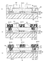
图2的(a)是示意性地表示本发明的中介层的一例的一部分的截面图。 (a) of FIG. 2 is a cross-sectional view schematically showing a part of an example of an interposer of the present invention. the
图2的(b)是示意性地表示在图2的(a)所示的中介层上设置保护膜并搭载了半导体元件的状态的一例的截面图。 FIG. 2( b ) is a cross-sectional view schematically showing an example of a state in which a protective film is provided on the interposer shown in FIG. 2( a ) and a semiconductor element is mounted thereon. the
本实施方式的中介层1具有:支承基板10;无机绝缘层20,其由无机材料构成;第一布线21,其形成在无机绝缘层20的内部;有机绝缘层30,其由有机材料构成;第二布线31,其形成在有机绝缘层30的表面上;以及通路导体,其作为电连接第一布线21和第二布线31的导体部。在图2的(b)中示出在本实施方式的中介层上还设置了保护膜40并搭载了半导体元件50的情形。
The
下面,参照图2的(a)以及图2的(b),从下侧起依次详细说明这些各部位。 Hereinafter, referring to FIG. 2( a ) and FIG. 2( b ), these parts will be described in detail sequentially from the bottom. the
首先,说明支承基板10。
First, the
作为本实施方式中的形成支承基板10的材料,可举出硅、氮化硅、碳化硅、氮化铝、多铝红柱石(Mullite)等。其中,从表面平坦度较高、能够形成微细布线这种观点出发,优选使用硅。
Examples of the material forming the
不特别限定该支承基板10的厚度,但是优选30~800μm。在支承基板10的厚度不足30μm的情况下,有可能无法确保中介层的刚性。另一方面,在支承基板10的厚度超过800μm的情况下,会导致中介层整体的厚度增加,因此不是优选。
The thickness of the
本实施方式中的无机绝缘层20是由SiO2(二氧化硅)、Si3N4(氮化硅)等无机材料构成的层。在本实施方式的中介层的制造方法的项目中说明具体的层结构的一例。
The inorganic insulating
第一布线21由多个通路连接盘22和电连接规定的通路连接盘22之间的布线部23构成。即,在形成在无机绝缘层20的内部的第一布线21的一部分上形成有与通路导体连接的通路连接盘22,规定的通路连接盘22之间通过布线部23相连接。
The
第一布线21在无机绝缘层20内部形成为包括通路连接盘22的表面的第一布线21的表面位于与无机绝缘层20的表面大致相同的平面上。
The
另外,第一布线21由镀铜以及镀铜之下的晶种层126构成。在本实施方式的中介层的制造方法的项目中说明晶种层的结构的一例。
In addition, the
在本实施方式中,通过镶嵌法来形成第一布线21,第一布线21的L/S与后述的第二布线31的L/S相比较小。
In this embodiment, the
此外,虽不特别限定第一布线的L/S,但期望L/S=1μm/1μm左右,也可以比它更细。 In addition, although the L/S of the first wiring is not particularly limited, it is desirable that L/S=about 1 μm/1 μm, and it may be thinner than this. the
此外,在此所说的第一布线的L/S是除去通路连接盘22以外的布线部23的L/S。
In addition, the L/S of the first wiring referred to here is the L/S of the
该第一布线21的厚度小于后述的第二布线的厚度。虽不特别限定本实施方式中的第一布线21的厚度,但优选在2μm以下。在第一布线21的厚度在2μm以下的情况下,除了能够进行布线的细化以外,工序变得简单,实现成本降低。
The thickness of the
另外,通过镶嵌法来形成第一布线21,因此由无机绝缘层20以及第一布线21构成的表面平坦。
In addition, since the
另外,在本实施方式中,通路连接盘22的直径大于后述的通路导体的直径。此外,在比较通路连接盘的直径和通路导体的直径时,只要比较通路连接盘与通路导体所接触的面之间的直径即可。
In addition, in this embodiment, the diameter of the via
本实施方式中的有机绝缘层30由有机材料构成,形成在无机绝缘层20上以及第一布线21上。该有机绝缘层30具有开口36(参照图6的(a)),在开口36中形成有作为导体部的通路导体32。并且,在有机绝缘层30的表面上形成有第二布线31。
The organic insulating
通路导体32的底面与通路连接盘22连接。
The bottom surface of via
并且,在形成在有机绝缘层30上的第二布线31的一部分上形成有焊盘34。并且,该第二布线31与第一布线21之间通过通路导体32而电连接。此外,焊盘34是在搭载半导体元件时通过焊料凸块等与半导体元件的连接端子连接的部位。
Furthermore, a
另外,第二布线31除了具有焊盘34以外还具有布线部33。
In addition, the
在图2的(a)以及图2的(b)中省略描绘了第二布线31的布线部33所连接的目的地(图中右侧),但是布线部33与规定的焊盘电连接。
In FIG. 2( a ) and FIG. 2( b ), the destination (right side in the figure) to which the
有机绝缘层30是由热固化性树脂、感光性树脂、在热固化性树脂的一部分上附加感光性基团而得到的树脂、热可塑性树脂、或者包含这些树脂的树脂复合物等构成的层。
The organic insulating
具体地说,期望由感光性聚酰亚胺树脂构成。 Specifically, it is desirable to be composed of a photosensitive polyimide resin. the
通路导体32以及第二布线31由镀铜以及镀铜之下的晶种层131构成。
The via
在本实施方式的中介层的制造方法的项目中说明晶种层的结构的一例。 An example of the structure of the seed layer will be described in the item of the method of manufacturing the interposer of the present embodiment. the
在本实施方式中,例如通过半添加法来形成通路导体32以及第二布线31,第二布线31的L/S与第一布线21的L/S相比较大。本实施方式中的第二布线的L/S为L/S=3μm/3μm,但是并不限于此。只要根据第二布线的条数以及形成第二布线的区域的面积等适当地决定即可。
In this embodiment, the via
此外,在此所说的第二布线31的L/S是除去焊盘34以外的布线部33的L/S。
In addition, the L/S of the
第二布线31的厚度大于第一布线21的厚度。不特别限定本实施方式中的第二布线31的厚度,但是优选大于2μm小于等于30μm。在第二布线31的厚度在该范围内的情况下,很好地抑制中介层的翘曲。并且,能够降低第二布线31的布线电阻。另外,也不会增加中介层的厚度。此外,第二布线的厚度意味着使用扫描型电子显微镜测量第二布线长度方向上的任意十个位置的截面而得到的各值的平均值。关于第一布线的厚度也相同。
The thickness of the
另外,第二布线的厚度相对于第一布线的厚度的比例大于1小于等于15。在上述第二布线的厚度相对于第一布线的厚度的比例不足1的情况下,无法充分确保中介层的刚性,有可能由于半导体元件与中介层之间的热膨胀系数的差异而在中介层上产生翘曲。另一方面,在上述第二布线的厚度相对于第一布线的厚度的比例超过15的情况下,当假设为布线宽度相同时,第二布线的厚宽比变大,例如在由于热历程而有机绝缘层膨胀收缩时第二布线容易跟踪该有机绝缘层的膨胀收缩,有可能使第二布线相对于有机绝缘层的密合性下降。 In addition, the ratio of the thickness of the second wiring to the thickness of the first wiring is greater than 1 and less than or equal to 15. When the ratio of the thickness of the second wiring to the thickness of the first wiring is less than 1, the rigidity of the interposer cannot be ensured sufficiently, and the interposer may be damaged due to the difference in thermal expansion coefficient between the semiconductor element and the interposer. produce warping. On the other hand, when the ratio of the thickness of the second wiring to the thickness of the first wiring exceeds 15, assuming that the width of the wiring is the same, the aspect ratio of the second wiring becomes large, for example, when the thickness of the second wiring is reduced due to thermal history. When the organic insulating layer expands and contracts, the second wiring tends to follow the expansion and contraction of the organic insulating layer, and the adhesiveness of the second wiring to the organic insulating layer may decrease. the
另外,期望第二布线31的截面面积相对于第一布线21的截面面积较大,特别期望是3~10倍。通过将第二布线的截面面积设为较大,第二布线的每单位长度的布线电阻变小。
In addition, the cross-sectional area of the
例如,在第一布线21和第二布线31的厚宽比都为1∶1的情况下,当设为第一布线的L/S=1μm/1μm、第二布线的L/S=3μm/3μm时,第二布线的截面面积为第一布线的截面面积的9倍。
For example, when the aspect ratios of the
此外,在比较第一布线21与第二布线31的截面面积情况下,比较各布线的布线部的截面面积。
In addition, when comparing the cross-sectional areas of the
另外,通路导体的高度(导体部的高度)h相对于第一布线的厚度的比例为小于等于5。由此,能够极力降低由于有机绝缘层的膨胀收缩而产生的应力对导体部的影响。该通路导体的高度 也使用扫描型电子显微镜来进行测量。 In addition, the ratio of the height of the via conductor (height of the conductor portion) h to the thickness of the first wiring is 5 or less. Thereby, the influence of the stress on the conductor part due to the expansion and contraction of the organic insulating layer can be reduced as much as possible. The height of the via conductors was also measured using a scanning electron microscope. the
接着,说明保护膜40以及半导体元件50。
Next, the
保护膜40形成在有机绝缘层30上以及第二布线31上。该保护膜40具有使焊盘34部分露出的开口。即,如图2的(b)所示,焊盘34的外缘部被保护膜40所覆盖。
The
不特别限定保护膜40的材料,但是从与有机绝缘层30之间的密合性的观点出发,优选有机材料。
The material of the
并且,在开口41上隔着势垒金属层43形成有由焊料构成的凸块42,半导体元件50通过该凸块42与中介层连接。
Furthermore, a
另外,底部填充树脂53被填充到半导体元件50与中介层之间。并且,半导体元件50被密封树脂51密封。
In addition, an
下面,使用附图说明本实施方式的中介层的制造方法。 Next, a method for manufacturing an interposer according to the present embodiment will be described with reference to the drawings. the
图3的(a)、图3的(b)以及图3的(c)、图4的(a)、图4的(b)以及图4的(c)是示意性地表示第一实施方式的中介层的制造工序的一部分的截面图。 Fig. 3(a), Fig. 3(b) and Fig. 3(c), Fig. 4(a), Fig. 4(b) and Fig. 4(c) schematically show the first embodiment A cross-sectional view of part of the interposer fabrication process. the
首先,如图3的(a)所示,在支承基板10上形成无机绝缘层20(例如第一SiO2层121、Si3N4层122以及第二SiO2层123)的薄膜。
First, as shown in FIG. 3( a ), a thin film of the inorganic insulating layer 20 (for example, the first SiO 2 layer 121 , the Si 3 N 4 layer 122 , and the second SiO 2 layer 123 ) is formed on the
使用硅片作为本实施方式的支承基板10,通过CVD(化学气相沉淀法(Chemical Vapor Deposition))法在硅片10的上面分别形成第一SiO2层121、Si3N4层122以及第二SiO2层123的薄膜。
Using a silicon wafer as the supporting
接着,通过涂敷抗蚀剂124并进行曝光、显影来对第二SiO2 层123去除要形成开口的规定位置的抗蚀剂124。 Next, the resist 124 is removed from the second SiO 2 layer 123 at predetermined positions where openings are to be formed by applying the resist 124 and performing exposure and development.
在图3的(b)中汇总示出这些工序。 These steps are collectively shown in (b) of FIG. 3 . the
接着,进行干蚀刻(反应性离子蚀刻),对没有形成抗蚀剂124的部分的第二SiO2层123进行蚀刻。 Next, dry etching (reactive ion etching) is performed to etch the second SiO 2 layer 123 where the resist 124 is not formed.
由此,在第二SiO2层123上形成如图3的(c)所示那样的图 案。 Thus, a pattern as shown in (c) of FIG. 3 is formed on the second SiO2 layer 123.
此外,在进行干蚀刻时,Si3N4层122起到蚀刻阻止层(Etching Stopper)的作用。 In addition, the Si 3 N 4 layer 122 functions as an etching stopper during dry etching.
接着,如图4的(a)所示,例如通过溅射在第二SiO2层123表面形成晶种层126。在本实施方式中,晶种层126由从下起依次为TaN、Ta、Cu的溅射膜构成,但是并不限于此。
Next, as shown in (a) of FIG. 4 , a
接着,如图4的(b)所示,将晶种层126作为供电层进行电解镀铜来形成电解镀铜层127。通过以往公知的方法进行电解镀铜即可。
Next, as shown in FIG. 4( b ), electrolytic copper plating is performed using the
接着,如图4的(c)所示,进行CMP(化学机械研磨)来去除电解镀铜层127以及第二SiO2层123表面的晶种层126。
Next, as shown in (c) of FIG. 4 , CMP (Chemical Mechanical Polishing) is performed to remove the electrolytic
此外,使用以往的镶嵌法中所知的方法以及装置来进行CMP即可。 In addition, CMP may be performed using methods and apparatuses known in conventional damascene methods. the
并且,在进行CMP之后残留的电解镀铜层成为包括通路连接盘22和布线部23的第一布线21。
In addition, the electrolytic copper plating layer remaining after the CMP becomes the
通过以上工序,能够形成无机绝缘层以及第一布线。 Through the above steps, the inorganic insulating layer and the first wiring can be formed. the
另外,也可以例如通过CVD在无机绝缘层以及第一布线的表面上形成Si3N4等的无机薄膜。设置该无机薄膜的目的在于提高有机绝缘层与无机绝缘层之间的密合性。 In addition, an inorganic thin film such as Si 3 N 4 may be formed on the surface of the inorganic insulating layer and the first wiring by, for example, CVD. The purpose of providing the inorganic thin film is to improve the adhesion between the organic insulating layer and the inorganic insulating layer.
图5的(a)、图5的(b)以及图5的(c)、图6的(a)、图6的(b)以及图6的(c)是示意性地表示第一实施方式的中介层的制造工序的一部分的截面图。 Fig. 5(a), Fig. 5(b) and Fig. 5(c), Fig. 6(a), Fig. 6(b) and Fig. 6(c) schematically show the first embodiment A cross-sectional view of part of the interposer fabrication process. the
首先,如图5的(a)所示,在无机绝缘层20以及第一布线21上形成有机绝缘层30,如图5的(b)所示那样形成开口36。
First, as shown in FIG. 5( a ), the organic insulating
作为形成有机绝缘层30的方法,例如能够使用以下方法:使用辊涂机来涂敷未固化的感光性聚酰亚胺树脂的方法等。
As a method of forming the organic insulating
作为形成开口的方法,能够使用曝光显影处理。 As a method of forming the opening, exposure and development processing can be used. the
接着,如图5的(c)所示,在有机绝缘层30的表面(包括开口36的壁面)和从开口36露出的通路连接盘22的上面形成晶种层131。
Next, as shown in FIG. 5( c ), a
晶种层131例如通过溅射来形成,在本实施方式中由Ti以及Cu构成。此外,晶种层131的结构并不限于此。
The
接着,如图6的(a)所示,设置抗镀层132,通过掩模对抗镀层132进行曝光、显影,由此去除要形成第二布线的位置的抗镀层132。 Next, as shown in FIG. 6( a ), the plating resist 132 is provided, and the plating resist 132 is exposed and developed through a mask to remove the plating resist 132 at the position where the second wiring is to be formed. the
作为抗镀层例如能够使用感光性干膜等。 As a plating resist, a photosensitive dry film etc. can be used, for example. the
接着,如图6的(b)所示,将晶种层131作为供电层进行电解镀铜,对去除了抗镀层132的部位实施镀铜。由此,在有机绝缘层30内形成通路导体32,并且,在有机绝缘层30上形成包括焊盘34和布线部33的第二布线31。
Next, as shown in FIG. 6( b ), electrolytic copper plating is performed using the
接着,如图6的(c)所示,去除残留的抗镀层,并且通过蚀刻来去除所去除的抗镀层下面的晶种层131。不特别限定对该晶种层131进行蚀刻的方法,但是从抑制电解镀铜的过蚀刻这种观点出发,优选干蚀刻(反应性离子蚀刻)。
Next, as shown in (c) of FIG. 6 , the remaining plating resist is removed, and the
通过以上工序,能够形成有机绝缘层以及第二布线。 Through the above steps, the organic insulating layer and the second wiring can be formed. the
图7的(a)以及图7的(b)是示意性地表示第一实施方式的中介层的制造工序的一部分的截面图。 7( a ) and 7 ( b ) are cross-sectional views schematically showing a part of the interposer manufacturing process of the first embodiment. the
首先,在有机绝缘层30上还形成其它有机绝缘层40。并且,在新形成的有机绝缘层40上形成开口41。该新形成的有机绝缘层40成为保护膜。
First, another organic insulating
在图7的(a)中汇总示出这些工序。 These steps are collectively shown in (a) of FIG. 7 . the
作为保护膜即有机绝缘层40,能够使用与有机绝缘层30相同的材料。另外,形成开口41的方法也能够使用与在有机绝缘层30上形成开口36的方法相同的方法。
As the organic insulating
接着,如图7的(b)所示,在设置于有机绝缘层40上的开口41内形成势垒金属层43。例如通过依次溅射氮化钽以及钽来形成该势垒金属层43。此外,不特别限定该势垒金属层43的构成材料以及形成方法。另外,虽然省略了图示,但是对从保护膜的开口露出的势垒金属层43的表面实施镀Ni/Au。这是为了在进行后述的焊料接合时确保焊料与焊盘之间的密合性。
Next, as shown in FIG. 7( b ), a
此外,只要根据需要进行保护膜的形成以及势垒金属层的形成即可。 In addition, what is necessary is just to perform formation of a protective film and formation of a barrier metal layer as needed. the
接着,说明在本实施方式的中介层上搭载半导体元件的工序。 Next, the process of mounting a semiconductor element on the interposer of this embodiment will be described. the
图8的(a)、图8的(b)是示意性地表示在第一实施方式的中介层上搭载半导体元件的工序的一例的截面图。 FIG. 8( a ) and FIG. 8( b ) are cross-sectional views schematically showing an example of a step of mounting a semiconductor element on an interposer in the first embodiment. the
首先,如图8的(a)所示,在势垒金属层43上形成由焊料构成的凸块42。
First, as shown in FIG. 8( a ), bumps 42 made of solder are formed on
接着,通过该凸块42将半导体元件50倒装安装在中介层上。
Next, the
然后,将底部填充树脂53填充到半导体元件50与中介层之间并使其固化。接着,用密封树脂51对所搭载的半导体元件50的周围进行密封。
Then, an
在图8的(b)中汇总示出这些工序。 These steps are collectively shown in (b) of FIG. 8 . the
此外,作为底部填充树脂以及密封树脂,使用公知的树脂即可。 In addition, known resins may be used as the underfill resin and the sealing resin. the
另外,在使用硅片作为支承基板、在硅片上形成中介层的情况下,通过针对中介层的尺寸使用足够大的硅片,能够在一片硅片上形成多个中介层。 Also, when using a silicon wafer as a supporting substrate and forming an interposer on the silicon wafer, a plurality of interposers can be formed on one silicon wafer by using a silicon wafer sufficiently large for the size of the interposer. the
在一片硅片上形成了多个中介层的情况下,在搭载半导体元件的工序之前或者搭载半导体元件的工序之后这种适当的时 期,通过切割等方法来切断硅片,由此能够按照每个中介层进行分割。由此,能够高效率地制造中介层。 When a plurality of interposers are formed on one silicon wafer, the silicon wafer can be cut by dicing or the like at an appropriate time before or after the process of mounting the semiconductor element, so that The intermediary layer is divided. Thereby, the interposer can be manufactured efficiently. the
下面,列举本实施方式的中介层以及中介层的制造方法的作用效果。 Next, the effects of the interposer and the method for manufacturing the interposer of the present embodiment will be listed. the
(1)在本实施方式的中介层中,在作为导体部的通路导体的底部周围存在有机绝缘层。因此,例如即使在由于半导体元件发热而通路导体膨胀的情况下,也能够由位于通路导体的底部周围的有机绝缘层缓和从通路导体接受的热应力。因此,能够抑制热应力集中到通路导体的底部,进而能够抑制在绝缘层内产生裂纹。 (1) In the interposer of the present embodiment, an organic insulating layer exists around the bottom of the via conductor as the conductor portion. Therefore, even when the via conductor expands due to heat generated by the semiconductor element, thermal stress received from the via conductor can be relieved by the organic insulating layer positioned around the bottom of the via conductor. Therefore, it is possible to suppress thermal stress from concentrating on the bottom of the via conductor, and it is also possible to suppress generation of cracks in the insulating layer. the
(2)另外,在有机绝缘层下面一体地设置有无机绝缘层。由此确保刚性,进而减轻有机绝缘层对通路导体的拉伸应力,因此能够抑制第一布线和通路导体剥离。 (2) In addition, an inorganic insulating layer is integrally provided under the organic insulating layer. As a result, rigidity is ensured, and tensile stress applied to the via conductor by the organic insulating layer is reduced, so that peeling between the first wiring and the via conductor can be suppressed. the
(3)另外,在最外层的有机绝缘层的表面上形成有保护膜,因此保护内部的布线层,能够抑制它们的损伤。 (3) In addition, since the protective film is formed on the surface of the outermost organic insulating layer, the internal wiring layers are protected and their damage can be suppressed. the
(4)另外,在无机绝缘层与有机绝缘层之间设置有无机薄膜,因此能够提高无机绝缘层与有机绝缘层之间的密合性。 (4) In addition, since the inorganic thin film is provided between the inorganic insulating layer and the organic insulating layer, the adhesiveness between the inorganic insulating layer and the organic insulating layer can be improved. the
(5)另外,本实施方式的中介层具有由硅构成的支承基板。通过具有支承基板,赋予中介层刚性,例如能够减小由热膨胀引起的中介层的翘曲。并且,由硅构成的支承基板平坦度极高,因此能够在其表面上形成微细的布线。除此之外,能够进一步抑制由所搭载的半导体元件与中介层之间的热膨胀系数的差异引起的中介层的翘曲。 (5) In addition, the interposer of the present embodiment has a supporting substrate made of silicon. By providing the support substrate, rigidity is imparted to the interposer, and warping of the interposer due to thermal expansion, for example, can be reduced. In addition, since the supporting substrate made of silicon has extremely high flatness, fine wiring can be formed on the surface. In addition to this, it is possible to further suppress warping of the interposer caused by a difference in thermal expansion coefficient between the mounted semiconductor element and the interposer. the
(6)另外,在本实施方式的中介层中,第二布线的厚度大于第一布线的厚度,第二布线的厚度相对于第一布线的厚度的比例大于1小于等于15。 (6) In addition, in the interposer of this embodiment, the thickness of the second wiring is greater than the thickness of the first wiring, and the ratio of the thickness of the second wiring to the thickness of the first wiring is greater than 1 and less than or equal to 15. the
这样,通过在与第一布线相比相对较厚的第二布线与杨氏 模量较大的无机绝缘层之间设置有机绝缘层而使有机绝缘层被杨氏模量较大的第二布线和无机绝缘层所狭持,因此赋予中介层刚性。其结果,抑制由上述热膨胀系数的差异引起的中介层的翘曲。另外,即使在由于热历程而有机绝缘层膨胀收缩时,也容易确保第二布线与有机绝缘层之间的密合。 In this way, by disposing an organic insulating layer between the second wiring relatively thicker than the first wiring and the inorganic insulating layer having a higher Young's modulus, the organic insulating layer is covered by the second wiring having a higher Young's modulus. and the inorganic insulating layer, thus imparting rigidity to the interposer. As a result, warpage of the interposer caused by the above-mentioned difference in thermal expansion coefficient is suppressed. In addition, even when the organic insulating layer expands and shrinks due to thermal history, it is easy to ensure close contact between the second wiring and the organic insulating layer. the
(7)另外,在本实施方式的中介层中,通路导体的高度相对于第一布线的厚度的比例为小于等于5。这样,能够极力降低由于有机绝缘层的膨胀收缩而产生的应力对通路导体的影响。 (7) In addition, in the interposer of the present embodiment, the ratio of the height of the via conductor to the thickness of the first wiring is 5 or less. In this way, the influence of stress on the via conductors due to expansion and contraction of the organic insulating layer can be minimized. the
(8)在本实施方式的中介层的制造方法中,在无机绝缘层的内部形成第一布线,在无机绝缘层上以及第一布线上形成有机绝缘层,形成电连接第二布线和第一布线的通路导体。 (8) In the method of manufacturing the interposer of this embodiment, the first wiring is formed inside the inorganic insulating layer, the organic insulating layer is formed on the inorganic insulating layer and the first wiring, and the second wiring and the first wiring are electrically connected. routed via conductors. the
通过这种工序,例如能够制造如下中介层:在半导体元件发热时也能够有效减少施加到通路导体的应力,进而在绝缘层内不会产生裂纹,并且不会产生通路部与通路连接盘之间的剥离。 Through this process, for example, an interposer can be produced that can effectively reduce the stress applied to the via conductor when the semiconductor element generates heat, and furthermore, no cracks will occur in the insulating layer, and no gap between the via portion and the via land will occur. stripping. the
(9)在本实施方式的中介层的制造方法中,通过镶嵌法来形成第一布线,通过半添加法来形成第二布线。 (9) In the interposer manufacturing method of this embodiment, the first wiring is formed by the damascene method, and the second wiring is formed by the semi-additive method. the
由此,能够高精确度地将第一布线形成为微细布线,并且能够形成平坦性较高的布线。另外,能够简单地形成布线电阻较低的第二布线来制造中介层。 Thereby, the first wiring can be formed as a fine wiring with high precision, and a wiring with high flatness can be formed. In addition, the interposer can be manufactured by simply forming the second wiring with low wiring resistance. the
(第二实施方式) (second embodiment)
本实施方式与上述第一实施方式的不同点在于没有支承基板10。
This embodiment differs from the first embodiment described above in that there is no
即,在如图8的(b)所示那样用密封树脂51对半导体元件50的周围进行密封之后,剥离支承基板10。不特别限定剥离支承基板的方法,但是能够通过磨削和蚀刻来进行。
That is, after the periphery of the
首先,使用磨削装置对由硅片构成的支承基板的第一面侧 (支承基板的表面露出的面)进行磨削,使支承基板的厚度变薄。不特别限定磨削量,但是期望磨削到支承基板的厚度为100μm左右为止。 First, the first surface side (the exposed surface of the support substrate) of the support substrate made of a silicon wafer is ground using a grinding device to reduce the thickness of the support substrate. The amount of grinding is not particularly limited, but it is desirable to grind until the thickness of the supporting substrate becomes about 100 μm. the
作为磨削装置,能够很好地使用用于磨削硅片的磨削装置。 As the grinding device, a grinding device for grinding a silicon wafer can be suitably used. the
接着,使用氢氧化钾等蚀刻液对通过磨削而变薄的支承基板(硅片)进行蚀刻处理来去除全部。作为使用于蚀刻的蚀刻液,只要能够使用于硅片的蚀刻就不特别进行限定,例如能够使用氢氧化钾水溶液等。不特别限定使用于蚀刻的装置,能够很好地使用用于硅片的湿蚀刻的装置。 Next, the support substrate (silicon wafer) thinned by grinding is etched using an etchant such as potassium hydroxide to remove all of it. The etchant used for etching is not particularly limited as long as it can be used for etching a silicon wafer, and for example, an aqueous potassium hydroxide solution or the like can be used. The apparatus used for etching is not particularly limited, and an apparatus used for wet etching of a silicon wafer can be suitably used. the
另外,在图3的(a)中,在支承基板10(硅片)上形成无机绝缘层20之前,也可以在支承基板10表面上形成剥离层。作为该剥离层的材料,可以是Cu、Ni等金属,或者也可以是树脂。在这种情况下,在剥离支承基板10时,通过剥离层能够容易地分离中介层和支承基板。不特别限定其方法,但是在剥离层为金属的情况下,使用蚀刻。在剥离层为树脂的情况下,例如可举出碱溶解等。在这种情况下,能够再次使用支承基板10(硅片)。
In addition, in FIG. 3( a ), before forming the inorganic insulating
图9是示意性地表示在第二实施方式的中介层上设置了加强件的情况的一例的截面图。 Fig. 9 is a cross-sectional view schematically showing an example of a case where a reinforcing member is provided on an interposer according to a second embodiment. the
在本实施方式的中介层2中,从提高其刚性这种观点出发,也可以通过粘接剂在中介层2的最表面上设置图9所示那样的加强件60。作为该加强件60的形状,例如可以如图9的(a)所示那样,是具备使由多个焊盘34构成的焊盘群61露出的开口部62的框状,例如也可以如图9的(b)所示那样,是具备使焊盘群61露出的凹部63的盖状。不特别限定该加强件的材料,但是从确保发热性这种观点出发,优选铜等金属材料。
In the interposer 2 of the present embodiment, from the viewpoint of increasing its rigidity, a
下面,列举本实施方式的中介层的制造方法的作用效果。 Next, the functions and effects of the method for manufacturing an interposer according to the present embodiment will be listed. the
(10)本实施方式的中介层的制造方法包括去除支承基板的 工序。 (10) The interposer manufacturing method of this embodiment includes the step of removing the supporting substrate. the
通过去除支承基板,能够制造厚度较薄、搭载了半导体元件时的安装高度较低的中介层。 By removing the support substrate, it is possible to manufacture an interposer having a thinner thickness and a lower mounting height when a semiconductor element is mounted thereon. the
(11)通过设置加强件来提高中介层的刚性。其结果,例如中介层也充分经得起由与半导体元件之间的热膨胀系数差引起的热应力,中介层整体不容易翘曲。因此,也抑制在半导体元件与中介层之间的接合部分(焊料凸块等外部连接端子)产生裂纹。 (11) Increase the rigidity of the interposer by setting reinforcements. As a result, for example, the interposer can sufficiently withstand the thermal stress caused by the difference in thermal expansion coefficient with the semiconductor element, and the entire interposer is less likely to warp. Therefore, it is also suppressed that cracks are generated in the bonding portion (external connection terminals such as solder bumps) between the semiconductor element and the interposer. the
(第三实施方式) (third embodiment)
下面,说明作为本发明的一个实施方式的第三实施方式。 Next, a third embodiment that is one embodiment of the present invention will be described. the
图10是示意性地表示本发明的中介层的另一例的一部分的截面图。 Fig. 10 is a cross-sectional view schematically showing part of another example of an interposer of the present invention. the
本实施方式的中介层3在没有支承基板10这点上与上述第二实施方式相同,但是能够在两面安装半导体元件这点与上述第二实施方式不同(参照图10)。
The
即,在无机绝缘层20以及第一布线21的下面形成有保护膜70,在该保护膜70上位于通路连接盘22正下方的位置处设置有开口71。并且,与第一实施方式同样地,在该开口71内隔着势垒金属层73形成有凸块72,半导体元件90通过该凸块72与中介层连接。
That is, the
另外,底部填充树脂93被填充到半导体元件90与中介层之间。并且,通过密封树脂91来密封半导体元件90。
In addition, an
下面示出本实施方式的中介层的制造方法。 The method for manufacturing the interposer of this embodiment is shown below. the
图11的(a)、图11的(b)、图11的(c)以及图11的(d)、图12的(a)、图12的(b)以及图12的(c)是示意性地表示第三实施方式的中介层的制造工序的一部分的截面图。 (a) of Fig. 11, (b) of Fig. 11, (c) of Fig. 11 and (d) of Fig. 11, (a) of Fig. 12, (b) of Fig. 12 and (c) of Fig. 12 are schematic is a cross-sectional view schematically showing a part of the interposer manufacturing process of the third embodiment. the
首先,如图11的(a)所示,通过CVD等在支承基板上依次形 成Si3N4层122以及SiO2层123,由此设置无机绝缘层20。接着,通过干蚀刻在该无机绝缘层20的期望的位置上形成开口125(图11的(b))。之后,与第一实施方式同样地形成晶种层126(图11的(c)),将该晶种层126作为供电层实施电解镀,通过CMP进行磨削来形成第一布线21(图11的(d))。
First, as shown in (a) of FIG. 11 , a Si 3 N 4 layer 122 and an SiO 2 layer 123 are sequentially formed on a support substrate by CVD or the like, whereby the inorganic insulating
之后,与上述第一实施方式同样地,形成有机绝缘层30、第二布线31等,搭载半导体元件50,进行到树脂密封为止(图12的(a))。
Thereafter, the organic insulating
接着,去除支承基板10,并使第一布线21以及无机绝缘层20的下面露出(图12的(b))。然后,在第一布线21以及无机绝缘层20的下面形成保护膜70,在位于通路连接盘22的正下方的位置处形成开口71。
Next, the supporting
之后,对开口进行势垒金属层73的形成以及凸块72的形成,安装半导体元件90(图12的(c))。
Thereafter, the barrier metal layer 73 and the
在本实施方式中能够发挥在第一实施方式中说明的效果(1)~(9)以及在第二实施方式中说明的效果(10)。 In this embodiment, the effects (1) to (9) described in the first embodiment and the effect (10) described in the second embodiment can be exhibited. the
在该第三实施方式中,也可以不安装半导体元件90而通过凸块72将中介层3搭载到印刷基板(母板)上。
In this third embodiment, the
(第四实施方式) (Fourth Embodiment)
下面,说明作为本发明的一个实施方式的第四实施方式。 Next, a fourth embodiment which is one embodiment of the present invention will be described. the
本实施方式的中介层为在第一实施方式中所说明的中介层中在无机绝缘层的内部或者有机绝缘层的表面上形成电源层和接地层中的至少一个。或者,也可以形成电容器等无源元件。 In the interposer of the present embodiment, at least one of the power supply layer and the ground layer is formed inside the inorganic insulating layer or on the surface of the organic insulating layer in the interposer described in the first embodiment. Alternatively, passive elements such as capacitors may also be formed. the
例如在无机绝缘层内形成了接地层的情况下,包括位于其正上方的第二布线在内形成微带(Microstrip)结构。其结果,能够匹配特性阻抗,能够使信号的传输稳定化。 For example, when the ground layer is formed in the inorganic insulating layer, a microstrip structure is formed including the second wiring located directly above it. As a result, characteristic impedance can be matched, and signal transmission can be stabilized. the
在本实施方式中能够发挥在第一实施方式中说明的效果 (1)~(9),并且能够发挥以下效果。 In this embodiment, the effects (1) to (9) described in the first embodiment can be exhibited, and the following effects can be exhibited. the
(12)通过在无机绝缘层或者有机绝缘层的没有形成布线的区域内设置电源层、接地层或者无源元件中的至少一个而有效地利用该区域,从而成为没有无用部分的高密度中介层。进而能够实现强化中介层的电源、提高信号特性、薄型化、小型化。 (12) By providing at least one of a power supply layer, a ground layer, or a passive element in a region where wiring is not formed in an inorganic insulating layer or an organic insulating layer, the region is effectively utilized, thereby becoming a high-density interposer without useless parts . Furthermore, it is possible to strengthen the power supply of the interposer, improve signal characteristics, and achieve thinning and miniaturization. the
(第五实施方式) (fifth embodiment)
下面,说明作为本发明的一个实施方式的第五实施方式。 Next, a fifth embodiment which is one embodiment of the present invention will be described. the
图13的(a)是示意性地表示本发明的中介层的另一例的一部分的截面图,图13的(b)是示意性地表示在图13的(a)所示的中介层上设置保护膜并搭载了半导体元件的状态的一例的截面图。 (a) of FIG. 13 is a cross-sectional view schematically showing a part of another example of the interposer of the present invention, and (b) of FIG. A cross-sectional view of an example of a state in which a semiconductor element is mounted with a protective film. the
本实施方式的中介层除了第一布线形成在无机绝缘层的表面以外与第一实施方式的中介层相同。下面,参照图13的(a)以及图13的(b)来详细说明这些本实施方式的中介层。 The interposer of this embodiment is the same as the interposer of the first embodiment except that the first wiring is formed on the surface of the inorganic insulating layer. Next, these interposers of this embodiment will be described in detail with reference to FIG. 13( a ) and FIG. 13( b ). the
在本实施方式的中介层4中,包括通路连接盘22以及布线部23的第一布线21形成在无机绝缘层20的表面上,第一布线21的表面位于无机绝缘层20的表面的上部。
In the interposer 4 of this embodiment, the
即,在通路连接盘22的底部存在无机绝缘层20。
That is, the inorganic insulating
其它结构与第一实施方式的中介层1相同,在无机绝缘层20上形成有具有开口的有机绝缘层30,在有机绝缘层的开口即通路连接盘22上形成有通路导体32。
The other structures are the same as the
并且,在有机绝缘层30上形成有具有焊盘34和布线部33的第二布线31。
Also, the
并且,在有机绝缘层30上以及第二布线上形成有保护膜40,并搭载有半导体元件50。
Furthermore, a
接着,关于本实施方式的中介层的制造方法,仅说明与第一实施方式的中介层的制造方法不同的工序。 Next, only the steps different from the interposer manufacturing method of the first embodiment will be described for the interposer manufacturing method of the present embodiment. the
图14的(a)、图14的(b)、图14的(c)、图14的(d)以及图14的(e)是示意性地表示第五实施方式的中介层的制造工序的一部分的截面图。 14( a ), FIG. 14( b ), FIG. 14( c ), FIG. 14( d ), and FIG. 14( e ) schematically show the manufacturing process of the interposer of the fifth embodiment. Sectional view of a part. the
如图14的(a)所示,在本实施方式的中介层的制造方法中,使用CVD在支承基板10上依次形成无机绝缘层20(例如第一SiO2层121、Si3N4层122以及第二SiO2层123)的薄膜。此外,无机绝缘层20的结构并不限于此。
As shown in (a) of FIG. 14 , in the interposer manufacturing method of this embodiment, the inorganic insulating layer 20 (such as a first SiO 2 layer 121, a Si 3 N 4 layer 122, etc.) is sequentially formed on a
接着,如图14的(b)所示,在无机绝缘层20的表面上形成金属层226。该金属层226例如通过溅射来形成,由Cu构成。
Next, as shown in FIG. 14( b ), a
接着,如图14的(c)所示,设置抗镀层224,通过掩模对抗镀层224进行曝光、显影,由此去除要形成第一布线的位置的抗镀层224。 Next, as shown in (c) of FIG. 14 , the plating resist 224 is provided, and the plating resist 224 is exposed and developed through a mask to remove the plating resist 224 at the position where the first wiring is to be formed. the
作为抗镀层例如能够使用感光性干膜等。 As a plating resist, a photosensitive dry film etc. can be used, for example. the
接着,如图14的(d)所示,将金属层226作为供电层进行电解镀铜,在去除了抗镀层224的部位上形成镀铜层227。
Next, as shown in (d) of FIG. 14 , electrolytic copper plating is performed using the
接着,如图14的(e)所示,去除抗镀层,并且通过蚀刻去除所去除的抗镀层下面的金属层226。
Next, as shown in (e) of FIG. 14 , the plating resist is removed, and the
通过以上工序,能够在无机绝缘层20的表面形成包括通路连接盘22以及布线部23的第一布线21。
Through the above steps, the
之后,与第一实施方式的中介层的制造方法同样地进行有机绝缘层的形成以后的工序,由此能够制造本实施方式的中介层。 Thereafter, the steps after the formation of the organic insulating layer are performed in the same manner as in the method of manufacturing the interposer of the first embodiment, whereby the interposer of the present embodiment can be manufactured. the
此外,对无机绝缘层20的表面形成通路连接盘22以及布线部23的工艺并不限于此。即,例如也可以在通过溅射在无机绝缘层20上形成金属膜226之后对该金属膜226进行蚀刻来形成期望的由通路连接盘22和布线部23构成的第一布线21。在本实施方式中也能够起到与上述第一实施方式相同的效果。
In addition, the process of forming the via
另外,在该第五实施方式中也可以与第二实施方式同样地去除支承基板。 In addition, also in this fifth embodiment, the supporting substrate may be removed in the same manner as in the second embodiment. the
(第六实施方式) (sixth embodiment)
下面,说明作为本发明的一个实施方式的第六实施方式。 Next, a sixth embodiment which is one embodiment of the present invention will be described. the
本实施方式的中介层为在第五实施方式中说明的中介层中在无机绝缘层或者有机绝缘层的表面上形成有电源层和接地层中的至少一个。或者,也可以形成电容器等无源元件。 The interposer of the present embodiment is one in which at least one of the power supply layer and the ground layer is formed on the surface of the inorganic insulating layer or the organic insulating layer in the interposer described in the fifth embodiment. Alternatively, passive elements such as capacitors may also be formed. the
作为在无机绝缘层的表面或者有机绝缘层的表面上设置电源层或者接地层的方法,能够使用与第四实施方式相同的方法。 As a method of providing a power supply layer or a ground layer on the surface of the inorganic insulating layer or the surface of the organic insulating layer, the same method as in the fourth embodiment can be used. the
在本实施方式中,除了发挥在第五实施方式中说明的效果以外,还能够发挥在第四实施方式中说明的(12)的效果。 In this embodiment, in addition to the effects described in the fifth embodiment, the effect of (12) described in the fourth embodiment can also be exhibited. the
(第七实施方式) (seventh embodiment)
在本实施方式的中介层中能够搭载多个半导体元件,构成为多个半导体元件中的特定的半导体元件之间仅通过第二布线相连接。 A plurality of semiconductor elements can be mounted on the interposer of the present embodiment, and specific semiconductor elements among the plurality of semiconductor elements are connected to each other only by the second wiring. the
图15是示意性地表示本发明的中介层的另一例的一部分的截面图。 Fig. 15 is a cross-sectional view schematically showing part of another example of an interposer of the present invention. the
在图15所示的中介层5中,能够搭载多个半导体元件50、52。
A plurality of
半导体元件50以及半导体元件52之间通过与凸块42连接的第二布线31相连接。
The
作为在该第七实施方式中使用的半导体元件50以及半导体元件52,例如半导体元件50为电源调节器模块,半导体元件52为CPU。
As the
仅通过第二布线连接这些半导体元件之间,由此能够降低半导体元件之间的布线的电阻。其结果,在第二布线中不会产生压降而能够对CPU等半导体元件施加适当的电压。 By connecting these semiconductor elements only through the second wiring, it is possible to reduce the resistance of the wiring between the semiconductor elements. As a result, an appropriate voltage can be applied to semiconductor elements such as a CPU without causing a voltage drop in the second wiring. the
此外,如果半导体元件之间的布线电阻不成问题,则也可以通过第一布线和第二布线连接半导体元件之间。 Furthermore, if the wiring resistance between the semiconductor elements is not a problem, the semiconductor elements may be connected via the first wiring and the second wiring. the
(第八实施方式) (eighth embodiment)
图16是示意性地表示本发明的中介层的另一例的一部分的截面图。 Fig. 16 is a cross-sectional view schematically showing a part of another example of the interposer of the present invention. the
在图16所示的中介层6中,在支承基板10内设置有贯通电极500。
In interposer 6 shown in FIG. 16 , penetrating
在这种情况下,中介层的表面和背面被电连接,在中介层的下面侧也能够安装半导体元件。另外,能够通过焊料凸块将中介层安装到印刷线路板(例如母板)上。 In this case, the front surface and the back surface of the interposer are electrically connected, and semiconductor elements can also be mounted on the lower surface of the interposer. Additionally, the interposer can be mounted to a printed wiring board (eg, motherboard) via solder bumps. the
贯通电极500由镀铜层501以及镀铜层之下的导体薄膜502构成。贯通电极500与支承基板10之间被绝缘膜503隔开,在支承基板10的背面侧也形成有绝缘膜503。
贯通电极500的上侧(支承基板的表面侧)与形成在无机绝缘层20内部的导体(图16中通路连接盘22)连接。
The upper side (the surface side of the support substrate) of the through
贯通电极500的下侧(支承基板的背面侧)与形成在支承基板10的背面上的焊盘600(布线)连接。即,形成在支承基板10的背面上的焊盘600(布线)和第一布线21(通路连接盘22)通过贯通电极500而电连接。
The lower side of the through electrode 500 (the back side of the support substrate) is connected to the pad 600 (wiring) formed on the back surface of the
另外,在焊盘600上形成有凸块542。通过该凸块542,在印刷线路板100上安装有中介层6。
In addition, bumps 542 are formed on the
底部填充树脂553被填充到印刷线路板100与中介层6之间。
此外,中介层6和印刷线路板100可以仅通过凸块542相连接,也可以通过凸块和引线两者相连接。
In addition, the interposer 6 and the printed
不特别限定绝缘膜503的材质,能够使用由SiO2膜等无机绝缘膜、树脂构成的有机绝缘膜。在此,举出使用有机绝缘膜作为绝缘膜503的例子。
The material of the insulating
第八实施方式的中介层的制造方法除了形成贯通电极的工序以外与第一实施方式的中介层的制造方法大致相同。因此,对第八实施方式的中介层的制造方法中的与第一实施方式的中介层的制造方法不同的工序进行说明。 The interposer manufacturing method of the eighth embodiment is substantially the same as the interposer manufacturing method of the first embodiment except for the step of forming the through-hole electrode. Therefore, the steps in the interposer manufacturing method of the eighth embodiment that are different from the interposer manufacturing method of the first embodiment will be described. the
图17的(a)、图17的(b)、图17的(c)、图17的(d)、图18的(a)、图18的(b)、图18的(c)、图19的(a)、图19的(b)以及图19的(c)是示意性地表示第八实施方式的中介层的制造工序的一部分的截面图。 (a) of Fig. 17, (b) of Fig. 17, (c) of Fig. 17, (d) of Fig. 17, (a) of Fig. 18, (b) of Fig. 18, (c) of Fig. 18, Fig. 19( a ), FIG. 19( b ), and FIG. 19( c ) are cross-sectional views schematically showing a part of the interposer manufacturing process of the eighth embodiment. the
在本实施方式中,与在第一实施方式的中介层的制造方法中示出的工序同样地,制作结构与在第一实施方式的说明中由图4的(c)示出的结构相同的基板(参照图17的(a))。 In this embodiment, similar to the steps shown in the interposer manufacturing method of the first embodiment, the same structure as that shown in FIG. substrate (see (a) of FIG. 17 ). the
接着,如图17的(b)所示,例如使用UV激光在支承基板10的规定位置形成开口510。不特别限定该开口510的形成方法,也可以采用干蚀刻(反应性离子蚀刻)、使用了碱溶液的湿蚀刻等。
Next, as shown in FIG. 17( b ), an
并且,如图17的(c)所示,对抗蚀剂511进行图案成形使得露出开口510。之后,将抗蚀剂511作为掩模进行干蚀刻(反应性离子蚀刻),依次对第一SiO2层121以及Si3N4层122进行蚀刻而使通路连接盘22的下面露出。
And, as shown in (c) of FIG. 17 , the resist 511 is patterned so that the
接着,如图17的(d)所示,例如使用浸涂法或者旋转涂敷法将液状树脂涂敷到支承基板10的背面侧,在大约200℃下将其干燥一小时来形成绝缘膜503。
Next, as shown in (d) of FIG. 17 , a liquid resin is applied to the back side of the
此时,在支承基板10的背侧表面和开口510的壁面上形成绝缘膜503。
At this time, an insulating
作为在该工序中使用的液状树脂,从后述那样能够容易地去除通路连接盘22表面的绝缘膜503这种观点出发,期望使用感光性树脂(例如JSR(株)社制,商品名称:WPR,型号:5100)。
As the liquid resin used in this step, it is desirable to use a photosensitive resin (such as JSR Co., Ltd., trade name: WPR) from the viewpoint that the insulating
具体地说,可举出如下构成的液状树脂:甲乙酮20~30重量%、乳酸乙酯20~30重量%、填料15~25重量%、酚醛清漆树脂5~15重量%、三聚氰胺类化合物1~10重量%、酚类树脂1~10重量%、交联橡胶1~10重量%、环氧类化合物1~5重量%、低分子酚醛树脂1~5重量%、偶联剂0.1~3重量%、三嗪类感光剂0.1~3重量%。 Specifically, a liquid resin having the following composition can be mentioned: 20 to 30% by weight of methyl ethyl ketone, 20 to 30% by weight of ethyl lactate, 15 to 25% by weight of filler, 5 to 15% by weight of novolac resin, 1 to 30% by weight of melamine compounds. 10% by weight, 1-10% by weight of phenolic resin, 1-10% by weight of cross-linked rubber, 1-5% by weight of epoxy compound, 1-5% by weight of low molecular phenolic resin, 0.1-3% by weight of coupling agent , 0.1 to 3% by weight of a triazine photosensitive agent. the
此外,作为有机绝缘膜的形成方法,除了旋转涂敷法、浸涂法以外,例如可举出真空蒸镀。 In addition, as a method of forming the organic insulating film, vacuum evaporation can be mentioned, for example, in addition to the spin coating method and the dip coating method. the
接着,如图18的(a)所示,通过与开口510对应的位置被开口的掩模512进行曝光。
Next, as shown in (a) of FIG. 18 , exposure is performed through a mask 512 opened at a position corresponding to the
并且,如图18的(b)所示,进行显影来去除所曝光的部位(开口510的底部)的绝缘膜503。
Then, as shown in FIG. 18( b ), development is performed to remove the insulating
通过上述工序,通路连接盘22的下面再次在支承基板10的背面侧露出。
Through the above steps, the lower surface of the via
接着,如图18的(c)所示,在所露出的通路连接盘22的下面以及绝缘膜503的表面上形成导体薄膜502。
Next, as shown in (c) of FIG. 18 , a conductive
导体薄膜502例如由Ni/Cu构成,通过溅射来形成。此外,该导体薄膜502的结构并不限于此。另外,作为导体薄膜502的形成方法不限于溅射,例如也可以采用无电解镀(NonElectrolytic Plating)。
The conductive
并且,如图19的(a)所示,将导体薄膜502作为供电层进行电解镀铜来形成镀铜层501。
Then, as shown in (a) of FIG. 19 , electrolytic copper plating is performed using the conductive
接着,如图19的(b)所示,在镀铜层501中形成焊盘的位置上形成抗蚀剂513。
Next, as shown in FIG. 19( b ), a resist 513 is formed on the
接着,如图19的(c)所示,通过蚀刻来去除没有形成抗蚀剂513的部位的镀铜层501以及导体薄膜502。
Next, as shown in (c) of FIG. 19 , the
通过上述工序,形成贯通电极500以及焊盘600。
Through the above steps, the through
在本实施方式中能够发挥在第一实施方式中说明的效果(1)~(9),并且能够发挥以下效果。 In this embodiment, the effects (1) to (9) described in the first embodiment can be exhibited, and the following effects can be exhibited. the
(13)通过在支承基板内形成贯通电极,中介层和印刷线路板通过焊料凸块相连接。其结果,与通过引线来连接双方的情况相比,缩短了布线距离。由此,抑制从印刷线路板至半导体元件的布线上的电阻增大,能够有效地抑制至半导体元件为止的压降。 (13) By forming penetrating electrodes in the support substrate, the interposer and the printed wiring board are connected by solder bumps. As a result, the wiring distance is shortened compared to the case where both are connected by lead wires. This suppresses an increase in resistance on the wiring from the printed wiring board to the semiconductor element, and effectively suppresses a voltage drop to the semiconductor element. the
(14)另外,本实施方式的中介层包括由有机树脂构成的绝缘膜,因此与形成无机绝缘膜作为绝缘膜的情况相比,中介层的热膨胀系数变大。因此,能够在一定程度上缓和主要由树脂构成的印刷线路板与中介层之间的热膨胀系数的不匹配,从而能够确保中介层与印刷线路板的连接部(凸块)的连接可靠性。 (14) In addition, since the interposer of the present embodiment includes an insulating film made of an organic resin, the thermal expansion coefficient of the interposer becomes larger than when an inorganic insulating film is formed as the insulating film. Therefore, the thermal expansion coefficient mismatch between the printed wiring board mainly made of resin and the interposer can be alleviated to some extent, and the connection reliability of the connection portion (bump) between the interposer and the printed wiring board can be ensured. the
(其它实施方式) (Other implementations)
作为电连接第一布线和第二布线的导体部,也可以是通孔导体。 Via-hole conductors may be used as the conductor portion that electrically connects the first wiring and the second wiring. the
不特别限定搭载在本发明的中介层上的半导体元件的种类、功能。另外,也不特别限定这样的半导体元件的个数以及搭载方式。即,也可以以层叠的状态安装多个半导体元件。在这种情况下,例如,设置在各半导体元件上的贯通电极之间通过焊料凸块进行连接。 The type and function of the semiconductor element mounted on the interposer of the present invention are not particularly limited. In addition, the number and mounting method of such semiconductor elements are not particularly limited, either. That is, a plurality of semiconductor elements may be mounted in a stacked state. In this case, for example, through-electrodes provided on the respective semiconductor elements are connected by solder bumps. the
另外,也可以设置多个无机绝缘层和/或有机绝缘层,从而第一布线和/或第二布线成为多层布线。 In addition, a plurality of inorganic insulating layers and/or organic insulating layers may be provided so that the first wiring and/or the second wiring becomes a multilayer wiring. the
只要构成第一布线、导体部以及第二布线的材料为导电性材料,就不特别进行限定。 Materials constituting the first wiring, the conductor portion, and the second wiring are not particularly limited as long as they are conductive materials. the
除了铜以外还可以举出镍、金、银等。 In addition to copper, nickel, gold, silver, etc. are mentioned. the
对于有机绝缘层的种类,作为热固化性树脂例如可举出环氧树脂、酚醛树脂、聚酰亚胺树脂、聚酯树脂、双马来酰亚胺 树脂、聚烯烃系树脂、聚苯醚树脂、聚苯树脂、氟树脂等。 For the type of organic insulating layer, examples of thermosetting resins include epoxy resins, phenolic resins, polyimide resins, polyester resins, bismaleimide resins, polyolefin resins, and polyphenylene ether resins. , polyphenylene resin, fluororesin, etc. the
另外,作为感光性树脂,例如可举出丙烯酸类树脂等。 Moreover, as photosensitive resin, acrylic resin etc. are mentioned, for example. the
作为对热固化性树脂的一部分赋予感光性基团而得到的树脂,可举出使上述热固化性树脂的热固化基团和甲基丙烯酸、丙烯酸进行丙烯酸化反应而得到的树脂等。另外,作为热可塑性树脂,例如可举出苯氧基树脂、聚醚砜(Polyether Sulfone:PES)、聚砜(Poly Sulfone:PSF)、聚苯砜(Polyphenylene Sulfone:PPS)、聚苯硫醚(Polyphenylene Sulfide:PPES)、聚苯醚(Polyphenylene Ether:PPE)、聚醚酰亚胺(Polyether Imide:PI)等。 Examples of the resin obtained by imparting a photosensitive group to a part of the thermosetting resin include resins obtained by acrylation reaction of the thermosetting group of the above-mentioned thermosetting resin with methacrylic acid and acrylic acid. In addition, examples of thermoplastic resins include phenoxy resins, polyether sulfone (PES), polysulfone (PSF), polyphenylene sulfone (PPS), polyphenylene sulfone ( Polyphenylene Sulfide: PPES), polyphenylene ether (Polyphenylene Ether: PPE), polyether imide (Polyether Imide: PI), etc. the
另外,作为能够使用于有机绝缘层的树脂复合物的具体组合,例如可举出酚醛树脂/聚醚砜、聚酰亚胺树脂/聚砜、环氧树脂/聚醚砜、环氧树脂/苯氧基树脂、丙烯酸类树脂/苯氧基树脂、将一部分环氧基丙烯酸化而得到的环氧树脂/聚醚砜等。 In addition, specific combinations of resin compounds that can be used in the organic insulating layer include, for example, phenolic resin/polyethersulfone, polyimide resin/polysulfone, epoxy resin/polyethersulfone, epoxy resin/benzene Oxygen resins, acrylic resins/phenoxy resins, epoxy resins/polyethersulfone obtained by acrylated epoxy groups, etc. the
关于通路连接盘的直径与通路导体的直径之间的关系,如果在能够确保通路连接盘与通路导体之间导通的范围内,则不特别进行限定,也可以是相同直径。 The relationship between the diameter of the via land and the diameter of the via conductor is not particularly limited as long as electrical conduction between the via land and the via conductor can be ensured, and may be the same diameter. the
另外,只要在通过镶嵌法来形成第一布线时使用的在无机绝缘层上形成的抗蚀剂的种类、曝光方法以及显影方法是在半导体制造工序中使用的抗蚀剂、曝光方法以及显影方法,就不特别进行限定。 In addition, as long as the type of resist formed on the inorganic insulating layer, the exposure method, and the development method used when forming the first wiring by the damascene method are those used in the semiconductor manufacturing process, the exposure method, and the development method , is not particularly limited. the
作为在无机绝缘层以及有机绝缘层上形成晶种层的方法,除了使用溅射以外,还能够使用被称为PVD(Physical VaporDeposition:物理气相沉淀)法的方法,具体地说,能够使用真空蒸镀、离子镀、电子束蒸镀等方法。 As a method of forming the seed layer on the inorganic insulating layer and the organic insulating layer, in addition to sputtering, a method called PVD (Physical Vapor Deposition: Physical Vapor Deposition) method can also be used. Specifically, vacuum evaporation can be used. Plating, ion plating, electron beam evaporation and other methods. the
另外,作为在有机绝缘层的表面形成晶种层的方法,还能够使用通过半添加法来形成导体电路而已知的以往公知的方 法。 In addition, as a method of forming a seed layer on the surface of the organic insulating layer, a conventionally known method of forming a conductive circuit by a semi-additive method can also be used. the
不特别限定形成有机绝缘层的方法,能够使用如下方法:利用旋转涂膜机、幕帘式涂布机等涂敷未固化的树脂的方法,通过对树脂膜进行热压接来形成树脂层的方法。 The method of forming the organic insulating layer is not particularly limited, and the following methods can be used: a method of applying an uncured resin using a spin coater, a curtain coater, etc., and a method of forming a resin layer by thermocompression bonding of a resin film. method. the
另外,使树脂固化的方法并不限于热固化。 In addition, the method of curing the resin is not limited to thermal curing. the
另外,作为在有机绝缘层上形成开口的方法并不限于曝光显影处理,还能够使用通过激光加工来开口的方法。 In addition, the method of forming openings in the organic insulating layer is not limited to exposure and development treatment, and a method of forming openings by laser processing can also be used. the
在这种情况下,可举出使用受激准分子激光器、UV-YAG激光器、二氧化碳激光器等的方法。 In this case, a method using an excimer laser, a UV-YAG laser, a carbon dioxide laser, or the like can be mentioned. the
Claims (18)
Applications Claiming Priority (5)
| Application Number | Priority Date | Filing Date | Title |
|---|---|---|---|
| US1743007P | 2007-12-28 | 2007-12-28 | |
| US61/017,430 | 2007-12-28 | ||
| US3894908P | 2008-03-24 | 2008-03-24 | |
| US61/038,949 | 2008-03-24 | ||
| PCT/JP2008/068383 WO2009084301A1 (en) | 2007-12-28 | 2008-10-09 | Interposer and interposer manufacturing method |
Publications (2)
| Publication Number | Publication Date |
|---|---|
| CN101632168A CN101632168A (en) | 2010-01-20 |
| CN101632168B true CN101632168B (en) | 2012-07-18 |
Family
ID=40824025
Family Applications (1)
| Application Number | Title | Priority Date | Filing Date |
|---|---|---|---|
| CN2008800078210A Active CN101632168B (en) | 2007-12-28 | 2008-10-09 | Interposer and interposer manufacturing method |
Country Status (7)
| Country | Link |
|---|---|
| US (2) | US8058563B2 (en) |
| EP (1) | EP2187439A1 (en) |
| JP (1) | JPWO2009084301A1 (en) |
| KR (1) | KR101089084B1 (en) |
| CN (1) | CN101632168B (en) |
| TW (1) | TW200929477A (en) |
| WO (1) | WO2009084301A1 (en) |
Families Citing this family (19)
| Publication number | Priority date | Publication date | Assignee | Title |
|---|---|---|---|---|
| EP2226841A1 (en) | 2007-12-28 | 2010-09-08 | Ibiden Co., Ltd. | Interposer and manufacturing method of the interposer |
| JP5456411B2 (en) * | 2009-08-19 | 2014-03-26 | ルネサスエレクトロニクス株式会社 | Semiconductor device and manufacturing method of semiconductor device |
| EP2339627A1 (en) * | 2009-12-24 | 2011-06-29 | Imec | Window interposed die packaging |
| WO2014069662A1 (en) * | 2012-11-05 | 2014-05-08 | 大日本印刷株式会社 | Wiring structure |
| JP6056490B2 (en) * | 2013-01-15 | 2017-01-11 | 株式会社ソシオネクスト | Semiconductor device and manufacturing method thereof |
| JP6908154B2 (en) * | 2015-10-28 | 2021-07-21 | 大日本印刷株式会社 | Interposer and manufacturing method of interposer |
| JP6699131B2 (en) * | 2015-10-28 | 2020-05-27 | 大日本印刷株式会社 | Interposer and method of manufacturing interposer |
| JP7043768B2 (en) * | 2017-09-28 | 2022-03-30 | 大日本印刷株式会社 | Through Electrode Substrate and Its Manufacturing Method |
| JP7087319B2 (en) * | 2017-09-28 | 2022-06-21 | 大日本印刷株式会社 | Through Silicon Via Board and Its Manufacturing Method |
| US11322449B2 (en) | 2017-10-31 | 2022-05-03 | Taiwan Semiconductor Manufacturing Co., Ltd. | Package with fan-out structures |
| TWI736780B (en) * | 2017-10-31 | 2021-08-21 | 台灣積體電路製造股份有限公司 | Chip package and methods of forming the same |
| JP2019161003A (en) | 2018-03-13 | 2019-09-19 | 株式会社東芝 | Semiconductor device and manufacturing method thereof |
| JP6986492B2 (en) * | 2018-06-01 | 2021-12-22 | 日東電工株式会社 | Wiring circuit board |
| JP7154913B2 (en) * | 2018-09-25 | 2022-10-18 | 株式会社東芝 | Semiconductor device and its manufacturing method |
| US11133263B2 (en) | 2019-09-17 | 2021-09-28 | Intel Corporation | High-density interconnects for integrated circuit packages |
| US11450622B2 (en) * | 2021-01-20 | 2022-09-20 | Taiwan Semiconductor Manufacturing Company, Ltd. | Semiconductor package |
| CN113299629B (en) * | 2021-04-09 | 2023-07-25 | 浙江毫微米科技有限公司 | Link unit and its preparation method, semiconductor packaging structure |
| CN115332215B (en) * | 2022-10-14 | 2023-03-24 | 北京华封集芯电子有限公司 | Interposer for chip packaging and manufacturing method |
| WO2025134670A1 (en) * | 2023-12-18 | 2025-06-26 | 株式会社ジャパンディスプレイ | Multilayer wiring board and method for producing same |
Citations (1)
| Publication number | Priority date | Publication date | Assignee | Title |
|---|---|---|---|---|
| JP2005317705A (en) * | 2004-04-28 | 2005-11-10 | Nec Corp | Semiconductor device, wiring board, and method of manufacturing wiring board |
Family Cites Families (16)
| Publication number | Priority date | Publication date | Assignee | Title |
|---|---|---|---|---|
| FR2666190B1 (en) * | 1990-08-24 | 1996-07-12 | Thomson Csf | METHOD AND DEVICE FOR HERMETIC ENCAPSULATION OF ELECTRONIC COMPONENTS. |
| US5310965A (en) * | 1991-08-28 | 1994-05-10 | Nec Corporation | Multi-level wiring structure having an organic interlayer insulating film |
| JPH10270496A (en) * | 1997-03-27 | 1998-10-09 | Hitachi Ltd | Electronic device, information processing device, semiconductor device, and semiconductor chip mounting method |
| US6037044A (en) * | 1998-01-08 | 2000-03-14 | International Business Machines Corporation | Direct deposit thin film single/multi chip module |
| US6252178B1 (en) * | 1999-08-12 | 2001-06-26 | Conexant Systems, Inc. | Semiconductor device with bonding anchors in build-up layers |
| JP3973340B2 (en) * | 1999-10-05 | 2007-09-12 | Necエレクトロニクス株式会社 | Semiconductor device, wiring board, and manufacturing method thereof |
| TWI312166B (en) * | 2001-09-28 | 2009-07-11 | Toppan Printing Co Ltd | Multi-layer circuit board, integrated circuit package, and manufacturing method for multi-layer circuit board |
| JP4343044B2 (en) | 2004-06-30 | 2009-10-14 | 新光電気工業株式会社 | Interposer, manufacturing method thereof, and semiconductor device |
| JP3961537B2 (en) * | 2004-07-07 | 2007-08-22 | 日本電気株式会社 | Manufacturing method of semiconductor mounting wiring board and manufacturing method of semiconductor package |
| JP4790297B2 (en) | 2005-04-06 | 2011-10-12 | ルネサスエレクトロニクス株式会社 | Semiconductor device and manufacturing method thereof |
| US7287325B2 (en) * | 2005-05-10 | 2007-10-30 | International Business Machines Corporation | Method of forming interconnect structure or interconnect and via structures using post chemical mechanical polishing |
| JP4716316B2 (en) | 2005-06-27 | 2011-07-06 | 次世代半導体材料技術研究組合 | Manufacturing method of semiconductor device |
| KR100731083B1 (en) * | 2005-07-28 | 2007-06-22 | 동부일렉트로닉스 주식회사 | Method of forming copper metal wiring and semiconductor device comprising copper metal wiring formed thereby |
| JP4819471B2 (en) * | 2005-10-12 | 2011-11-24 | 日本電気株式会社 | Wiring substrate, semiconductor device using the wiring substrate, and manufacturing method thereof |
| US20070128465A1 (en) * | 2005-12-05 | 2007-06-07 | General Electric Company | Transparent electrode for organic electronic devices |
| JP4950743B2 (en) | 2007-04-17 | 2012-06-13 | 株式会社フジクラ | Multilayer wiring board and manufacturing method thereof |
-
2008
- 2008-10-09 CN CN2008800078210A patent/CN101632168B/en active Active
- 2008-10-09 WO PCT/JP2008/068383 patent/WO2009084301A1/en not_active Ceased
- 2008-10-09 KR KR1020097017443A patent/KR101089084B1/en active Active
- 2008-10-09 EP EP08868937A patent/EP2187439A1/en not_active Withdrawn
- 2008-10-09 JP JP2009531506A patent/JPWO2009084301A1/en active Pending
- 2008-11-14 TW TW097144282A patent/TW200929477A/en unknown
- 2008-12-29 US US12/345,295 patent/US8058563B2/en active Active
-
2011
- 2011-07-15 US US13/183,742 patent/US20110265323A1/en not_active Abandoned
Patent Citations (1)
| Publication number | Priority date | Publication date | Assignee | Title |
|---|---|---|---|---|
| JP2005317705A (en) * | 2004-04-28 | 2005-11-10 | Nec Corp | Semiconductor device, wiring board, and method of manufacturing wiring board |
Also Published As
| Publication number | Publication date |
|---|---|
| US20090175023A1 (en) | 2009-07-09 |
| US20110265323A1 (en) | 2011-11-03 |
| CN101632168A (en) | 2010-01-20 |
| JPWO2009084301A1 (en) | 2011-05-12 |
| US8058563B2 (en) | 2011-11-15 |
| EP2187439A1 (en) | 2010-05-19 |
| WO2009084301A1 (en) | 2009-07-09 |
| KR101089084B1 (en) | 2011-12-06 |
| KR20090125755A (en) | 2009-12-07 |
| TW200929477A (en) | 2009-07-01 |
Similar Documents
| Publication | Publication Date | Title |
|---|---|---|
| CN101632168B (en) | Interposer and interposer manufacturing method | |
| US8373069B2 (en) | Electronic component mounting substrate and method for manufacturing electronic component mounting substrate | |
| JP3677429B2 (en) | Method of manufacturing flip chip type semiconductor device | |
| US7843059B2 (en) | Electronic parts packaging structure | |
| JP4973743B2 (en) | Semiconductor device mounting substrate and method for manufacturing semiconductor device mounting substrate | |
| JP2012033973A (en) | Wiring board and semiconductor package | |
| JP5362569B2 (en) | Interposer and method of manufacturing interposer | |
| US20110221071A1 (en) | Electronic device and manufacturing method of electronic device | |
| US8178790B2 (en) | Interposer and method for manufacturing interposer | |
| CN101632170B (en) | Interposer and method for manufacturing interposer | |
| JP4170266B2 (en) | Wiring board manufacturing method | |
| TW202312374A (en) | Stiffener frame for semiconductor device packages | |
| JP7172105B2 (en) | Wiring substrate, semiconductor device having wiring substrate, and method for manufacturing semiconductor device | |
| JP3834305B2 (en) | Manufacturing method of multilayer wiring board | |
| JP2023005239A (en) | Wiring board, wiring board manufacturing method, and intermediate product |
Legal Events
| Date | Code | Title | Description |
|---|---|---|---|
| C06 | Publication | ||
| PB01 | Publication | ||
| C10 | Entry into substantive examination | ||
| SE01 | Entry into force of request for substantive examination | ||
| C14 | Grant of patent or utility model | ||
| GR01 | Patent grant |