JP3982082B2 - Manufacturing method of semiconductor device - Google Patents
Manufacturing method of semiconductor device Download PDFInfo
- Publication number
- JP3982082B2 JP3982082B2 JP27409498A JP27409498A JP3982082B2 JP 3982082 B2 JP3982082 B2 JP 3982082B2 JP 27409498 A JP27409498 A JP 27409498A JP 27409498 A JP27409498 A JP 27409498A JP 3982082 B2 JP3982082 B2 JP 3982082B2
- Authority
- JP
- Japan
- Prior art keywords
- region
- semiconductor wafer
- cutting line
- semiconductor device
- semiconductor
- Prior art date
- Legal status (The legal status is an assumption and is not a legal conclusion. Google has not performed a legal analysis and makes no representation as to the accuracy of the status listed.)
- Expired - Lifetime
Links
- 239000004065 semiconductor Substances 0.000 title claims description 233
- 238000004519 manufacturing process Methods 0.000 title claims description 44
- 239000011347 resin Substances 0.000 claims description 81
- 229920005989 resin Polymers 0.000 claims description 81
- 238000000034 method Methods 0.000 claims description 50
- 230000002093 peripheral effect Effects 0.000 claims description 10
- 238000012545 processing Methods 0.000 claims description 5
- 238000012790 confirmation Methods 0.000 claims description 4
- 239000010408 film Substances 0.000 description 74
- 239000000758 substrate Substances 0.000 description 27
- 229910000679 solder Inorganic materials 0.000 description 17
- 239000010409 thin film Substances 0.000 description 12
- 230000015572 biosynthetic process Effects 0.000 description 9
- 238000007789 sealing Methods 0.000 description 7
- 239000011248 coating agent Substances 0.000 description 5
- 238000000576 coating method Methods 0.000 description 5
- 238000007598 dipping method Methods 0.000 description 4
- 239000000463 material Substances 0.000 description 4
- 239000004593 Epoxy Substances 0.000 description 3
- 239000011521 glass Substances 0.000 description 3
- 238000012546 transfer Methods 0.000 description 3
- PCHJSUWPFVWCPO-UHFFFAOYSA-N gold Chemical compound [Au] PCHJSUWPFVWCPO-UHFFFAOYSA-N 0.000 description 2
- 239000010931 gold Substances 0.000 description 2
- 229910052737 gold Inorganic materials 0.000 description 2
- 239000002184 metal Substances 0.000 description 2
- 229910052751 metal Inorganic materials 0.000 description 2
- 238000007740 vapor deposition Methods 0.000 description 2
- 238000013461 design Methods 0.000 description 1
- 230000009977 dual effect Effects 0.000 description 1
- 230000000694 effects Effects 0.000 description 1
- 238000003780 insertion Methods 0.000 description 1
- 230000037431 insertion Effects 0.000 description 1
- 230000010354 integration Effects 0.000 description 1
- WABPQHHGFIMREM-UHFFFAOYSA-N lead(0) Chemical compound [Pb] WABPQHHGFIMREM-UHFFFAOYSA-N 0.000 description 1
- 238000007726 management method Methods 0.000 description 1
- 238000012986 modification Methods 0.000 description 1
- 230000004048 modification Effects 0.000 description 1
- 238000012858 packaging process Methods 0.000 description 1
- 238000003908 quality control method Methods 0.000 description 1
- 238000012827 research and development Methods 0.000 description 1
- 238000005476 soldering Methods 0.000 description 1
- QERYCTSHXKAMIS-UHFFFAOYSA-M thiophene-2-carboxylate Chemical compound [O-]C(=O)C1=CC=CS1 QERYCTSHXKAMIS-UHFFFAOYSA-M 0.000 description 1
Images


Classifications
-
- H—ELECTRICITY
- H01—ELECTRIC ELEMENTS
- H01L—SEMICONDUCTOR DEVICES NOT COVERED BY CLASS H10
- H01L24/00—Arrangements for connecting or disconnecting semiconductor or solid-state bodies; Methods or apparatus related thereto
- H01L24/01—Means for bonding being attached to, or being formed on, the surface to be connected, e.g. chip-to-package, die-attach, "first-level" interconnects; Manufacturing methods related thereto
- H01L24/10—Bump connectors ; Manufacturing methods related thereto
- H01L24/12—Structure, shape, material or disposition of the bump connectors prior to the connecting process
-
- H—ELECTRICITY
- H01—ELECTRIC ELEMENTS
- H01L—SEMICONDUCTOR DEVICES NOT COVERED BY CLASS H10
- H01L25/00—Assemblies consisting of a plurality of semiconductor or other solid state devices
-
- H—ELECTRICITY
- H01—ELECTRIC ELEMENTS
- H01L—SEMICONDUCTOR DEVICES NOT COVERED BY CLASS H10
- H01L21/00—Processes or apparatus adapted for the manufacture or treatment of semiconductor or solid state devices or of parts thereof
- H01L21/02—Manufacture or treatment of semiconductor devices or of parts thereof
- H01L21/04—Manufacture or treatment of semiconductor devices or of parts thereof the devices having potential barriers, e.g. a PN junction, depletion layer or carrier concentration layer
- H01L21/50—Assembly of semiconductor devices using processes or apparatus not provided for in a single one of the groups H01L21/18 - H01L21/326 or H10D48/04 - H10D48/07 e.g. sealing of a cap to a base of a container
- H01L21/56—Encapsulations, e.g. encapsulation layers, coatings
- H01L21/565—Moulds
-
- H—ELECTRICITY
- H01—ELECTRIC ELEMENTS
- H01L—SEMICONDUCTOR DEVICES NOT COVERED BY CLASS H10
- H01L23/00—Details of semiconductor or other solid state devices
- H01L23/28—Encapsulations, e.g. encapsulating layers, coatings, e.g. for protection
- H01L23/31—Encapsulations, e.g. encapsulating layers, coatings, e.g. for protection characterised by the arrangement or shape
- H01L23/3107—Encapsulations, e.g. encapsulating layers, coatings, e.g. for protection characterised by the arrangement or shape the device being completely enclosed
- H01L23/3114—Encapsulations, e.g. encapsulating layers, coatings, e.g. for protection characterised by the arrangement or shape the device being completely enclosed the device being a chip scale package, e.g. CSP
-
- H—ELECTRICITY
- H01—ELECTRIC ELEMENTS
- H01L—SEMICONDUCTOR DEVICES NOT COVERED BY CLASS H10
- H01L24/00—Arrangements for connecting or disconnecting semiconductor or solid-state bodies; Methods or apparatus related thereto
- H01L24/01—Means for bonding being attached to, or being formed on, the surface to be connected, e.g. chip-to-package, die-attach, "first-level" interconnects; Manufacturing methods related thereto
- H01L24/10—Bump connectors ; Manufacturing methods related thereto
- H01L24/11—Manufacturing methods
-
- H—ELECTRICITY
- H01—ELECTRIC ELEMENTS
- H01L—SEMICONDUCTOR DEVICES NOT COVERED BY CLASS H10
- H01L24/00—Arrangements for connecting or disconnecting semiconductor or solid-state bodies; Methods or apparatus related thereto
- H01L24/01—Means for bonding being attached to, or being formed on, the surface to be connected, e.g. chip-to-package, die-attach, "first-level" interconnects; Manufacturing methods related thereto
- H01L24/10—Bump connectors ; Manufacturing methods related thereto
- H01L24/15—Structure, shape, material or disposition of the bump connectors after the connecting process
- H01L24/16—Structure, shape, material or disposition of the bump connectors after the connecting process of an individual bump connector
-
- H—ELECTRICITY
- H01—ELECTRIC ELEMENTS
- H01L—SEMICONDUCTOR DEVICES NOT COVERED BY CLASS H10
- H01L24/00—Arrangements for connecting or disconnecting semiconductor or solid-state bodies; Methods or apparatus related thereto
- H01L24/93—Batch processes
- H01L24/94—Batch processes at wafer-level, i.e. with connecting carried out on a wafer comprising a plurality of undiced individual devices
-
- H—ELECTRICITY
- H01—ELECTRIC ELEMENTS
- H01L—SEMICONDUCTOR DEVICES NOT COVERED BY CLASS H10
- H01L2224/00—Indexing scheme for arrangements for connecting or disconnecting semiconductor or solid-state bodies and methods related thereto as covered by H01L24/00
- H01L2224/01—Means for bonding being attached to, or being formed on, the surface to be connected, e.g. chip-to-package, die-attach, "first-level" interconnects; Manufacturing methods related thereto
- H01L2224/10—Bump connectors; Manufacturing methods related thereto
- H01L2224/12—Structure, shape, material or disposition of the bump connectors prior to the connecting process
- H01L2224/13—Structure, shape, material or disposition of the bump connectors prior to the connecting process of an individual bump connector
- H01L2224/13001—Core members of the bump connector
- H01L2224/1302—Disposition
- H01L2224/13022—Disposition the bump connector being at least partially embedded in the surface
-
- H—ELECTRICITY
- H01—ELECTRIC ELEMENTS
- H01L—SEMICONDUCTOR DEVICES NOT COVERED BY CLASS H10
- H01L2224/00—Indexing scheme for arrangements for connecting or disconnecting semiconductor or solid-state bodies and methods related thereto as covered by H01L24/00
- H01L2224/01—Means for bonding being attached to, or being formed on, the surface to be connected, e.g. chip-to-package, die-attach, "first-level" interconnects; Manufacturing methods related thereto
- H01L2224/10—Bump connectors; Manufacturing methods related thereto
- H01L2224/12—Structure, shape, material or disposition of the bump connectors prior to the connecting process
- H01L2224/13—Structure, shape, material or disposition of the bump connectors prior to the connecting process of an individual bump connector
- H01L2224/13001—Core members of the bump connector
- H01L2224/13099—Material
- H01L2224/131—Material with a principal constituent of the material being a metal or a metalloid, e.g. boron [B], silicon [Si], germanium [Ge], arsenic [As], antimony [Sb], tellurium [Te] and polonium [Po], and alloys thereof
-
- H—ELECTRICITY
- H01—ELECTRIC ELEMENTS
- H01L—SEMICONDUCTOR DEVICES NOT COVERED BY CLASS H10
- H01L2224/00—Indexing scheme for arrangements for connecting or disconnecting semiconductor or solid-state bodies and methods related thereto as covered by H01L24/00
- H01L2224/01—Means for bonding being attached to, or being formed on, the surface to be connected, e.g. chip-to-package, die-attach, "first-level" interconnects; Manufacturing methods related thereto
- H01L2224/10—Bump connectors; Manufacturing methods related thereto
- H01L2224/15—Structure, shape, material or disposition of the bump connectors after the connecting process
- H01L2224/16—Structure, shape, material or disposition of the bump connectors after the connecting process of an individual bump connector
-
- H—ELECTRICITY
- H01—ELECTRIC ELEMENTS
- H01L—SEMICONDUCTOR DEVICES NOT COVERED BY CLASS H10
- H01L2224/00—Indexing scheme for arrangements for connecting or disconnecting semiconductor or solid-state bodies and methods related thereto as covered by H01L24/00
- H01L2224/01—Means for bonding being attached to, or being formed on, the surface to be connected, e.g. chip-to-package, die-attach, "first-level" interconnects; Manufacturing methods related thereto
- H01L2224/26—Layer connectors, e.g. plate connectors, solder or adhesive layers; Manufacturing methods related thereto
- H01L2224/27—Manufacturing methods
- H01L2224/274—Manufacturing methods by blanket deposition of the material of the layer connector
-
- H—ELECTRICITY
- H01—ELECTRIC ELEMENTS
- H01L—SEMICONDUCTOR DEVICES NOT COVERED BY CLASS H10
- H01L2924/00—Indexing scheme for arrangements or methods for connecting or disconnecting semiconductor or solid-state bodies as covered by H01L24/00
- H01L2924/0001—Technical content checked by a classifier
- H01L2924/00013—Fully indexed content
-
- H—ELECTRICITY
- H01—ELECTRIC ELEMENTS
- H01L—SEMICONDUCTOR DEVICES NOT COVERED BY CLASS H10
- H01L2924/00—Indexing scheme for arrangements or methods for connecting or disconnecting semiconductor or solid-state bodies as covered by H01L24/00
- H01L2924/01—Chemical elements
- H01L2924/01004—Beryllium [Be]
-
- H—ELECTRICITY
- H01—ELECTRIC ELEMENTS
- H01L—SEMICONDUCTOR DEVICES NOT COVERED BY CLASS H10
- H01L2924/00—Indexing scheme for arrangements or methods for connecting or disconnecting semiconductor or solid-state bodies as covered by H01L24/00
- H01L2924/01—Chemical elements
- H01L2924/01005—Boron [B]
-
- H—ELECTRICITY
- H01—ELECTRIC ELEMENTS
- H01L—SEMICONDUCTOR DEVICES NOT COVERED BY CLASS H10
- H01L2924/00—Indexing scheme for arrangements or methods for connecting or disconnecting semiconductor or solid-state bodies as covered by H01L24/00
- H01L2924/01—Chemical elements
- H01L2924/01006—Carbon [C]
-
- H—ELECTRICITY
- H01—ELECTRIC ELEMENTS
- H01L—SEMICONDUCTOR DEVICES NOT COVERED BY CLASS H10
- H01L2924/00—Indexing scheme for arrangements or methods for connecting or disconnecting semiconductor or solid-state bodies as covered by H01L24/00
- H01L2924/01—Chemical elements
- H01L2924/01015—Phosphorus [P]
-
- H—ELECTRICITY
- H01—ELECTRIC ELEMENTS
- H01L—SEMICONDUCTOR DEVICES NOT COVERED BY CLASS H10
- H01L2924/00—Indexing scheme for arrangements or methods for connecting or disconnecting semiconductor or solid-state bodies as covered by H01L24/00
- H01L2924/01—Chemical elements
- H01L2924/01033—Arsenic [As]
-
- H—ELECTRICITY
- H01—ELECTRIC ELEMENTS
- H01L—SEMICONDUCTOR DEVICES NOT COVERED BY CLASS H10
- H01L2924/00—Indexing scheme for arrangements or methods for connecting or disconnecting semiconductor or solid-state bodies as covered by H01L24/00
- H01L2924/01—Chemical elements
- H01L2924/01039—Yttrium [Y]
-
- H—ELECTRICITY
- H01—ELECTRIC ELEMENTS
- H01L—SEMICONDUCTOR DEVICES NOT COVERED BY CLASS H10
- H01L2924/00—Indexing scheme for arrangements or methods for connecting or disconnecting semiconductor or solid-state bodies as covered by H01L24/00
- H01L2924/01—Chemical elements
- H01L2924/01075—Rhenium [Re]
-
- H—ELECTRICITY
- H01—ELECTRIC ELEMENTS
- H01L—SEMICONDUCTOR DEVICES NOT COVERED BY CLASS H10
- H01L2924/00—Indexing scheme for arrangements or methods for connecting or disconnecting semiconductor or solid-state bodies as covered by H01L24/00
- H01L2924/01—Chemical elements
- H01L2924/01079—Gold [Au]
-
- H—ELECTRICITY
- H01—ELECTRIC ELEMENTS
- H01L—SEMICONDUCTOR DEVICES NOT COVERED BY CLASS H10
- H01L2924/00—Indexing scheme for arrangements or methods for connecting or disconnecting semiconductor or solid-state bodies as covered by H01L24/00
- H01L2924/01—Chemical elements
- H01L2924/01082—Lead [Pb]
-
- H—ELECTRICITY
- H01—ELECTRIC ELEMENTS
- H01L—SEMICONDUCTOR DEVICES NOT COVERED BY CLASS H10
- H01L2924/00—Indexing scheme for arrangements or methods for connecting or disconnecting semiconductor or solid-state bodies as covered by H01L24/00
- H01L2924/013—Alloys
- H01L2924/014—Solder alloys
-
- H—ELECTRICITY
- H01—ELECTRIC ELEMENTS
- H01L—SEMICONDUCTOR DEVICES NOT COVERED BY CLASS H10
- H01L2924/00—Indexing scheme for arrangements or methods for connecting or disconnecting semiconductor or solid-state bodies as covered by H01L24/00
- H01L2924/10—Details of semiconductor or other solid state devices to be connected
- H01L2924/11—Device type
- H01L2924/13—Discrete devices, e.g. 3 terminal devices
- H01L2924/1304—Transistor
- H01L2924/1306—Field-effect transistor [FET]
- H01L2924/13091—Metal-Oxide-Semiconductor Field-Effect Transistor [MOSFET]
-
- H—ELECTRICITY
- H01—ELECTRIC ELEMENTS
- H01L—SEMICONDUCTOR DEVICES NOT COVERED BY CLASS H10
- H01L2924/00—Indexing scheme for arrangements or methods for connecting or disconnecting semiconductor or solid-state bodies as covered by H01L24/00
- H01L2924/10—Details of semiconductor or other solid state devices to be connected
- H01L2924/11—Device type
- H01L2924/14—Integrated circuits
-
- H—ELECTRICITY
- H01—ELECTRIC ELEMENTS
- H01L—SEMICONDUCTOR DEVICES NOT COVERED BY CLASS H10
- H01L2924/00—Indexing scheme for arrangements or methods for connecting or disconnecting semiconductor or solid-state bodies as covered by H01L24/00
- H01L2924/15—Details of package parts other than the semiconductor or other solid state devices to be connected
- H01L2924/151—Die mounting substrate
- H01L2924/153—Connection portion
- H01L2924/1531—Connection portion the connection portion being formed only on the surface of the substrate opposite to the die mounting surface
- H01L2924/15311—Connection portion the connection portion being formed only on the surface of the substrate opposite to the die mounting surface being a ball array, e.g. BGA
Landscapes
- Engineering & Computer Science (AREA)
- Microelectronics & Electronic Packaging (AREA)
- Computer Hardware Design (AREA)
- Power Engineering (AREA)
- Physics & Mathematics (AREA)
- Condensed Matter Physics & Semiconductors (AREA)
- General Physics & Mathematics (AREA)
- Manufacturing & Machinery (AREA)
- Dicing (AREA)
- Encapsulation Of And Coatings For Semiconductor Or Solid State Devices (AREA)
- Wire Bonding (AREA)
Description
【0001】
【発明の属する技術分野】
本発明は半導体装置の製造方法に関し、特に、小型化および高密度化されたパッケージ形態を有する半導体装置の製造方法に関する。
【0002】
【従来の技術】
近年のVLSIなどの半導体装置においては、3年で7割の縮小化を実現し、高集積化及び高性能化を達成してきた。これに伴い、半導体装置のパッケージ形態も小型化、高密度化が達成されてきた。
【0003】
従来、半導体装置のパッケージ形態としては、DIP(Dual Inline Package )あるいはPGA(Pin Grid Array)などのプリント基板に設けたスルーホールにリード線を挿入して実装するリード挿入型(THD:Through Hall Mount Device )や、QFP(Quad Flat (L-Leaded) Package)あるいはTCP(Tape Carrier Package)などのリード線を基板の表面にハンダ付けして実装する表面実装型(SMD:Surface Mount Device)が用いられてきた。さらに、出力端子をエリア化したBGA(Ball Grid Array )パッケージに代表されるパッケージ形態に移行してきている。
【0004】
一方で、半導体装置の小型化、高密度化に対する要求はさらに高まりつつあり、上記のQFPなどのパッケージ形態では対応できなくなってきている。このため、半導体チップにパッケージサイズを限りなく近づけてさらなる小型化、高密度化を実現するチップサイズパッケージ(CSP:Chip Size Package 、FBGA(Fine-Pitch BGA)とも呼ばれる)と呼ばれるパッケージ形態が注目を集めており、現在活発に研究がなされ、多くの提案が示されている。
【0005】
上記のCSP形態の半導体装置と、これを実装する方法について説明する。例えば図8(a)の断面図に示すように、半導体チップ10aの図示しないパッド電極とベースボード(インタポーザ)11とが、はんだなどのバンプ12により機械的、電気的に接続されている。さらに、半導体チップ10aとベースボード11の間隙部には、バンプ12による接合を保護するための封止樹脂13が充填され、封止されている。さらに、ベースボード11の半導体チップ10aと接続している面の反対側の面には、実装基板と接続するためのはんだなどのバンプ14が形成されている。バンプ14は、半導体チップ10aのパッド電極とベースボード11とを接続しているバンプ12に対して、ベースボード11中に形成された図示しないスルーホールなどの配線部を介して接続されている。これらにより、CSP形態の半導体装置100が形成されている。
【0006】
上記の半導体装置100を実装するための実装基板2は、例えばガラスエポキシ系材料よりなる基板20の上面において、実装する半導体装置100のバンプ14の形成位置に対応する位置に形成されたランド(電極)21と、ランド21に接続して、基板20の表面上あるいは裏面上、もしくは両面上に形成されている図示しないプリント配線部を有している。上記の半導体装置100を上記の実装基板2に実装するには、実装基板2のランド21形成面に対して、半導体装置100のバンプ14の形成面から、それぞれ対応するランド21とバンプ14を位置合わせしてマウントし、図8(b)に示すように、バンプ14をリフローさせるなどの方法により、半導体装置100と実装基板2のランド21とをバンプ14を介して機械的、電気的に接続する。
【0007】
上記の半導体装置100は、半導体チップ10aと実装基板2の間に緩衝材となるベースボード(インタポーザ)11を有しているが、さらなる小型化、低コスト化および電子回路の処理速度の向上のために、上記のベースボード(インタポーザ)を用いず、ウェーハレベルでパッケージ化処理を施す形態のCSPについての研究開発が現在活発になされている。
【0008】
上記のベースボード(インタポーザ)を用いないCSP形態の半導体装置と、これを実装する方法について説明する。例えば図9(a)の断面図に示すように、半導体チップ10aの図示しないパッド電極に接続してはんだなどのバンプ12が形成されている。バンプ12の間隙部における半導体チップ10a表面は、樹脂被膜15により封止されている。これらにより、CSP形態の半導体装置1が形成されている。一方、上記の半導体装置1を実装するための実装基板2は、上記と同様に、例えばガラスエポキシ系材料よりなる基板20の上面にランド(電極)21と、図示しないプリント配線部を有している。上記の半導体装置1を上記の実装基板2に実装するには、実装基板2のランド21形成面に対して、半導体装置1のバンプ12の形成面から、それぞれ対応するランド21とバンプ12を位置合わせしてマウントし、図9(b)に示すように、バンプ12をリフローさせるなどの方法により、半導体装置1と実装基板2のランド21とをバンプ12を介して機械的、電気的に接続する。
【0009】
上記のCSP形態の半導体装置1の製造方法について図面を参照して説明する。まず、図10(a)に示すように、半導体チップの回路パターンが形成された半導体ウェーハ10上に、半導体チップの回路パターンに接続するようにはんだなどのバンプ12aを形成する。
【0010】
次に、図10(b)に示すように、上記の半導体ウェーハ10全体を溶融樹脂中に浸漬し、バンプ12aの間隙部を封止しながら、バンプ12aを完全に埋める膜厚で、半導体ウェーハ10のバンプ12a形成面上に樹脂被膜15を形成する。ここで、溶融樹脂中に浸漬する方法(ディッピング法)では、半導体ウェーハ10の両面に樹脂被膜15が形成される。
【0011】
次に、図11(c)に示すように、半導体ウェーハ10のバンプ12a形成面上から、バンプ12aの一部が露出するまで樹脂被膜15を研削して薄膜化する。
【0012】
次に、図11(d)に示すように、バンプ12aに接続させてはんだボール12bを転写する。バンプ12aとはんだボール12bとから、バンプ12が構成されている。
【0013】
次に、図11(e)に示すように、半導体ウェーハ10上に形成された半導体チップの回路パターンの間の領域であり、半導体ウェーハ10の切り代となる領域である切断ラインに沿って、半導体ウェーハ10を切断し(ダイシング工程)、個々に切断された半導体チップ10aを有するCSP形態の各半導体装置1と、半導体ウェーハ10の外周部分であり、完全な回路パターンを有していない不要な部分3とに分割する。
【0014】
上記の製造方法により製造する半導体装置1は、半導体ウェーハ10をダイシング処理して、そのまま実装基板に実装することが可能であり、従来のベースボード(インタポーザ)を用いた半導体装置に比べて、コストの削減および納期の短縮が可能である。
【0015】
【発明が解決しようとする課題】
しかしながら、上記の半導体装置の製造方法においては、半導体ウェーハ上の切り代となる切断ラインに沿って、正確に位置を合わせて半導体ウェーハを切断することが難しい。これは、例えば図12(a)に示すような回路パターンと、各パターンに接続するバンプ12を有し、各回路パターンの間の領域が切断ライン16となる半導体ウェーハ10に対して、樹脂被膜を形成すると、図12(b)に示すように、半導体ウェーハ10上の全領域で各回路パターンの間の領域である切断ライン16が覆われてしまうために、この状態でX1 〜X6 およびY1 〜Y6 の各切断ラインに沿って切断しようとしても、切断ラインの位置を確認することができなくなるためである。また、切断した位置が実際に上記の切断ラインに沿っているか確認することも困難であり、半導体装置の製造工程の品質管理上でも正確な管理が困難となっていた。
【0016】
本発明は上記の問題を鑑みなされたものであり、本発明は、表面にバンプを有する半導体チップのバンプ形成面上のバンプの間隙部が樹脂で封止されたパッケージ形態の半導体装置を製造するためのダイシング工程において、半導体ウェーハ上の切り代となる切断ラインに正確に位置を合わせて半導体ウェーハを切断することができる半導体装置の製造方法を提供することを目的とする。
【0017】
【課題を解決するための手段】
上記の目的を達成するため、本発明の半導体装置の製造方法は、表面にバンプを有する半導体チップのバンプ形成面上において、前記バンプの間隙部が樹脂で封止されたパッケージ形態の半導体装置の製造方法であって、半導体ウェーハの中央部の領域を第1領域とし、前記半導体ウェーハの外周側の領域を第2領域として、少なくとも前記第1領域において複数個の前記半導体チップの回路パターンを形成し、前記第1領域と前記第2領域にわたって前記半導体チップ間の切断ラインを形成する工程と、前記半導体ウェーハ上に、少なくとも前記第1領域において、前記半導体チップの回路パターンに接続するようにバンプを形成する工程と、前記第1領域においては前記バンプの間隙部を封止しながら所定の膜厚で、前記第2領域の少なくとも前記切断ラインの一部を含む領域においては前記切断ラインの一部の位置を確認できる膜厚で、前記半導体ウェーハのバンプ形成面上に樹脂被膜を形成する工程と、前記第2領域の前記切断ラインの一部を含む領域において確認される切断ラインを基準位置とし、前記切断ラインに沿って前記半導体ウェーハを切断する工程とを有する。
【0018】
上記の本発明の半導体装置の製造方法は、半導体ウェーハの中央部の領域を第1領域とし、半導体ウェーハの外周側の領域を第2領域として、少なくとも第1領域において複数個の半導体チップの回路パターンを形成し、第1領域と第2領域にわたって半導体チップ間の切断ラインを形成し、次に、少なくとも第1領域において、半導体チップの回路パターンに接続するようにバンプを形成する。次に、第1領域においてはバンプの間隙部を封止しながら所定の膜厚で、第2領域の少なくとも切断ラインの一部を含む領域においては切断ラインの一部の位置を確認できる膜厚で、半導体ウェーハのバンプ形成面上に樹脂被膜を形成する。次に、第2領域の前記切断ラインの一部を含む領域において確認される切断ラインを基準位置とし、切断ラインに沿って半導体ウェーハを切断する。
【0019】
上記の本発明の半導体装置の製造方法によれば、第1領域においてはバンプの間隙部を封止しながら所定の膜厚で、第2領域の少なくとも切断ラインの一部を含む領域においては切断ラインの一部の位置を確認できる膜厚で、半導体ウェーハのバンプ形成面上に樹脂被膜を形成するので、後工程で半導体ウェーハを切断するときに、第2領域の少なくとも切断ラインの一部を含む領域において切断ラインの位置を確認することが可能であり、半導体ウェーハ上の切り代となる切断ラインに正確に位置を合わせて半導体ウェーハを切断することができる。
【0020】
上記の本発明の半導体装置の製造方法は、半導体ウェーハの中央部の領域を第1領域とし、半導体ウェーハの外周側の領域を第2領域として、少なくとも第1領域において複数個の半導体チップの回路パターンを形成し、第1領域と第2領域にわたって半導体チップ間の切断ラインを形成する。
第2領域の少なくとも一部上では樹脂被膜の膜厚を薄く形成してしまうので、半導体装置としては使えない領域となってしまうが、半導体ウェーハの外周側の領域は元々完全な回路パターンを有していない不要な部分であるので、この領域を利用して第2領域とすることができる。
【0021】
上記の本発明の半導体装置の製造方法は、好適には、前記半導体ウェーハのバンプ形成面上に樹脂被膜を形成する工程が、前記第1領域および前記第2領域において所定の膜厚で樹脂被膜を形成する工程と、前記第2領域の少なくとも前記切断ラインの一部を含む領域において前記切断ラインの一部の位置を確認できる膜厚となるまで前記樹脂被膜を薄膜化する工程とを含む。第2領域において厚膜に形成してしまっても、薄膜化することで切断ラインの一部の位置を確認できるようにすることができる。
【0022】
上記の本発明の半導体装置の製造方法は、好適には、前記第1領域および前記第2領域において所定の膜厚で樹脂被膜を形成する工程においては、前記半導体ウェーハを溶融樹脂中に浸漬して前記樹脂被膜を形成する。これにより、1領域および第2領域において所定の膜厚で樹脂被膜を形成することができる。
【0023】
上記の本発明の半導体装置の製造方法は、好適には、前記半導体ウェーハのバンプ形成面上に樹脂被膜を形成する工程においては、前記第1領域においては所定の膜厚となり、前記第2領域の少なくとも前記切断ラインの一部を含む領域においては前記切断ラインの一部の位置を確認できる膜厚となるような型を用いて前記樹脂被膜を形成する。これにより、第2領域において切断ラインの一部の位置を確認できるように薄膜に形成することができる。
【0024】
上記の本発明の半導体装置の製造方法は、好適には、前記半導体ウェーハのバンプ形成面上に樹脂被膜を形成する工程においては、前記第2領域の少なくとも前記切断ラインの一部を含む領域において膜厚が30μm以下となるように前記樹脂被膜を形成する。これにより、切断ラインの一部の位置を確認できる膜厚とすることができる。
【0025】
上記の本発明の半導体装置の製造方法は、好適には、前記半導体ウェーハのバンプ形成面上に樹脂被膜を形成する工程においては、前記第1領域において前記バンプを完全に埋める膜厚で前記樹脂被膜を形成し、前記半導体ウェーハを切断する工程の前に、前記第1領域において、少なくとも前記バンプの一部を露出させるまで前記樹脂被膜を薄膜化する工程をさらに有する。これにより、バンプの一部が露出して、実装基板に実装するときに電気的に接続することが可能となる。
【0026】
上記の本発明の半導体装置の製造方法は、好適には、前記半導体ウェーハを切断する工程においては、前記半導体ウェーハの画像を撮影し、コンピュータ上で画像処理して前記切断ラインの位置を確認する。半導体装置の設計ルールが、例えば0.35μmから0.25μmあるいは0.18μmとますます微細化されるに従い、上記の半導体チップ間に切断ラインも幅が狭められていき、目視で確認することが困難となっても、コンピュータ上で画像処理を行うことにより確実に切断ラインの位置を確認することができる。
【0027】
【発明の実施の形態】
以下に、本発明の半導体装置の製造方法の実施の形態について、図面を参照して説明する。
【0028】
第1実施形態
本実施形態にかかる半導体装置は、図1(a)の断面図に示すように、半導体チップ10aの図示しないパッド電極に接続してはんだなどのバンプ12が形成されており、バンプ12の間隙部における半導体チップ10a表面は、樹脂被膜15により封止されている。半導体チップ10aのバンプ12形成面と反対側の表面上も樹脂被膜で被覆されていてもよい。これらにより、CSP形態の半導体装置1が形成されている。
【0029】
上記の半導体装置1を実装するための実装基板2としては、図1(a)中に示すように、例えばガラスエポキシ系材料よりなる基板20の上面にランド(電極)21と、図示しないプリント配線部を有している。上記の半導体装置1を上記の実装基板2に実装するには、実装基板2のランド21形成面に対して、半導体装置1のバンプ12の形成面から、それぞれ対応するランド21とバンプ12を位置合わせしてマウントし、図1(b)に示すように、バンプ12をリフローさせるなどの方法により、半導体装置1と実装基板2のランド21とをバンプ12を介して機械的、電気的に接続する。
【0030】
上記のCSP形態の半導体装置1の製造方法について図面を参照して説明する。まず、図2(a)に示すように、半導体ウェーハ10上に半導体チップの回路パターン(不図示)と、半導体チップ間の切断ライン(不図示)を形成する。ここで、半導体チップの完全な回路パターンが形成されている半導体ウェーハ10の中央部の領域を第1領域Aとし、完全な回路パターンを有しておらず、不要な領域となる半導体ウェーハ10の外周側の領域を第2領域Bとする。半導体チップ間の切断ラインは、第1領域Aから第2領域Bにわたって形成する。次に、少なくとも第1領域Aにおいて、半導体チップの回路パターンに接続するように、蒸着法あるいは転写法などにより、はんだあるいは金などからなるバンプ12aを形成する。
【0031】
次に、図2(b)に示すように、上記の半導体ウェーハ10全体を溶融樹脂中に浸漬し、第1領域Aにおいてバンプ12aの間隙部を封止しながら、バンプ12aを完全に埋める膜厚で、第1領域Aおよび第2領域Bにおいて、半導体ウェーハ10のバンプ12a形成面上に樹脂被膜15を形成する。ここで、溶融樹脂中に浸漬する方法(ディッピング法)では、半導体ウェーハ10の両面に樹脂被膜15が形成されるが、バンプ12a形成面の裏面側の樹脂被膜は必ずしも形成しなくてもよい。
【0032】
次に、図2(c)に示すように、第2領域Bの少なくとも切断ラインの一部を含む領域において、切断ラインの一部の位置を確認できる膜厚となるまで樹脂被膜15を薄膜化する。第2領域Bの一部である薄膜領域16aにおいては、樹脂被膜15の膜厚が例えば20〜30μmとなっており、樹脂被膜の下層のパターンが透けて見えるため、切断ラインの一部の位置を確認することができる。
【0033】
次に、図3(d)に示すように、第1領域Aにおいて、少なくともバンプ12aの一部を露出させるまで樹脂被膜15を研削して薄膜化する.
【0034】
次に、図3(e)に示すように、第1領域Aにおいて、バンプ12aに接続させてはんだボール12bを転写する。バンプ12aとはんだボール12bとから、バンプ12が構成されている。
【0035】
次に、図3(f)に示すように、第1領域Aおよび第2領域Bにおいて半導体ウェーハ10上に形成された半導体チップの回路パターンの間の領域であり、半導体ウェーハ10の切り代となる領域である切断ラインに沿って、半導体ウェーハ10を切断し(ダイシング工程)、個々に切断された半導体チップ10aを有するCSP形態の各半導体装置1と、半導体ウェーハ10の外周部分であり、完全な回路パターンを有していない不要な部分3とに分割する。ここで、切断ラインに沿って半導体ウェーハ10を切断するにあたっては、第2領域B中に形成された薄膜領域16aにおいて、薄い樹脂被膜15を通して透けて見える下層のパターンから切断ラインの位置を目視によって確認し、あるいは、半導体ウェーハ10の画像をCCDカメラなどで撮影し、得られた画像をコンピュータ上で画像処理して、切断ラインの位置を確認し、確認された切断ラインを基準位置として切断ラインに沿って半導体ウェーハ10を切断する。
【0036】
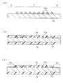
上記の半導体装置の製造方法においては、例えば図4に示すような回路パターンと、各パターンに接続するバンプ12を有し、各回路パターンの間の領域が切断ライン16となる半導体ウェーハ10に対して、樹脂被膜15を形成するが、図5(a)あるいは図5(b)に示すように、半導体ウェーハ10上の完全な回路パターンを有していない不要な部分となる領域中の切断ラインの一部を含む領域(例えば図5(a)および(b)に示すように、半導体ウェーハ上から4か所選択する)において、切断ラインの一部の位置を確認できる膜厚となるまで樹脂被膜15を薄膜化して形成することにより、この薄膜領域16aにおいては、樹脂被膜の下層のパターンが透けて見えるため、切断ライン16の位置を確認することができ、X1 〜X6 およびY1 〜Y6 の各切断ラインに沿って半導体ウェーハ10を切断するときに、半導体ウェーハ10上の切り代となる切断ライン16に正確に位置を合わせて半導体ウェーハ10を切断することができる。
【0037】
第2実施形態
本実施形態にかかる半導体装置は、第1実施形態にかかる半導体装置と実質的に同一であり、説明を省略する。
【0038】
本実施形態にかかる半導体装置の製造方法について図面を参照して説明する。まず、図6(a)に示すように、半導体ウェーハ10上に半導体チップの回路パターン(不図示)と、半導体チップ間の切断ライン(不図示)を形成する。ここで、半導体チップの完全な回路パターンが形成されている半導体ウェーハ10の中央部の領域を第1領域Aとし、完全な回路パターンを有しておらず、不要な領域となる半導体ウェーハ10の外周側の領域を第2領域Bとする。半導体チップ間の切断ラインは、第1領域Aから第2領域Bにわたって形成する。次に、少なくとも第1領域Aにおいて、半導体チップの回路パターンに接続するように、蒸着法あるいは転写法などにより、はんだあるいは金などからなるバンプ12aを形成する。
【0039】
次に、図6(b)に示すように、第1金型30の上に上記の半導体ウェーハを戴置し、その上に樹脂タブレット15aを戴置する。その上方から第2金型31を押しつけ、タブレット状の樹脂を溶融し、第1領域Aにおいてバンプ12aの間隙部を封止しながら再固化させ、半導体ウェーハ10のバンプ12a形成面上に樹脂被膜15を形成する。ここで、上記の半導体ウェーハ10の第1領域Aにおいてはバンプ12aを完全に埋める膜厚で、第2領域Bの少なくとも切断ラインの一部を含む領域においては、切断ラインの一部の位置を確認できる膜厚となるような第1金型30および第2金型31の対を用いることで、図6(c)に示すように、第2領域Bの一部である薄膜領域16aにおける樹脂被膜15の膜厚を20〜30μmとすることができ、樹脂被膜の下層のパターンが透けて見えるために、切断ラインの一部の位置を確認することができる。
【0040】
次に、図7(d)に示すように、第1領域Aにおいて、少なくともバンプ12aの一部を露出させるまで樹脂被膜15を研削して薄膜化する.
【0041】
次に、図7(e)に示すように、第1領域Aにおいて、バンプ12aに接続させてはんだボール12bを転写する。バンプ12aとはんだボール12bとから、バンプ12が構成されている。
【0042】
次に、図7(f)に示すように、第1領域Aおよび第2領域Bにおいて半導体ウェーハ10上に形成された半導体チップの回路パターンの間の領域であり、半導体ウェーハ10の切り代となる領域である切断ラインに沿って、半導体ウェーハ10を切断し(ダイシング工程)、個々に切断された半導体チップ10aを有するCSP形態の各半導体装置1と、半導体ウェーハ10の外周部分であり、完全な回路パターンを有していない不要な部分3とに分割する。ここで、切断ラインに沿って半導体ウェーハ10を切断するにあたっては、第2領域B中に形成された薄膜領域16aにおいて、薄い樹脂被膜15を通して透けて見える下層のパターンから切断ラインの位置を確認し、あるいは、半導体ウェーハ10の画像をCCDカメラなどで撮影し、得られた画像をコンピュータ上で画像処理して、確認された切断ラインを基準位置として切断ラインに沿って半導体ウェーハ10を切断する。
【0043】
上記の半導体装置の製造方法においては、第1実施形態と同様に、上記の薄膜領域16aにおいて、樹脂被膜の下層のパターンが透けて見えるため、切断ライン16の位置を確認することができ、X1 〜X6 およびY1 〜Y6 の各切断ラインに沿って半導体ウェーハ10を切断するときに、半導体ウェーハ10上の切り代となる切断ライン16に正確に位置を合わせて半導体ウェーハ10を切断することができる。金型を用いて形成する薄膜領域としては、図5(a)あるいは図5(b)に示すようなパターンとすることができる。
【0044】
本発明の半導体装置としては、MOSトランジスタ系半導体装置、バイポーラ系半導体装置、BiCMOS系半導体装置、ロジックとメモリを搭載した半導体装置など、半導体装置であれば何にでも適用可能である。
【0045】
本発明の半導体装置は上記の実施の形態に限定されない。例えば、第2領域において、切断ラインが確認できるように樹脂被膜を薄膜化する際に、薄膜領域においては樹脂被膜を完全に除去してしまってもかまわない。樹脂被膜は最初からバンプの一部が露出する膜厚で形成することも可能である。その他、本発明の要旨を逸脱しない範囲で種々の変更が可能である。
【0046】
【発明の効果】
上記のように、本発明の半導体装置の製造方法によれば、第1領域においてはバンプの間隙部を封止しながら所定の膜厚で、第2領域の少なくとも切断ラインの一部を含む領域においては切断ラインの一部の位置を確認できる膜厚で、半導体ウェーハのバンプ形成面上に樹脂被膜を形成するので、後工程で半導体ウェーハを切断するときに、第2領域の少なくとも切断ラインの一部を含む領域において切断ラインの位置を確認することが可能であり、半導体ウェーハ上の切り代となる切断ラインに正確に位置を合わせて半導体ウェーハを切断することができる。
【図面の簡単な説明】
【図1】図1は第1実施形態にかかる半導体装置と、その実装基板への実装方法を説明する断面図であり、(a)は実装基板への半導体装置のマウント工程まで、(b)はリフロー工程までをそれぞれ示す。
【図2】図2は第1実施形態にかかる半導体装置の製造方法の製造工程を示す断面図であり、(a)はバンプの形成工程まで、(b)は樹脂被膜の形成工程まで、(c)は第2領域の一部における樹脂被膜の薄膜化工程までを示す。
【図3】図3は図2の続きの工程を示し、(d)は第1領域における樹脂被膜の薄膜化工程まで、(e)はバンプへのはんだボールの転写工程まで、(f)は切断ラインに沿って半導体ウェーハを切断する工程までを示す。
【図4】図4は第1実施形態にかかる半導体装置の製造方法の製造工程のバンプの形成工程後の半導体ウェーハの斜視図である。
【図5】図5は第1実施形態にかかる半導体装置の製造方法の製造工程の第2領域の一部に薄膜領域を形成する工程後の半導体ウェーハの斜視図である。
【図6】図6は第2実施形態にかかる半導体装置の製造方法の製造工程を示す断面図であり、(a)はバンプの形成工程まで、(b)は金型への半導体ウェーハの戴置工程まで、(c)は樹脂被膜の形成工程までを示す。
【図7】図7は図6の続きの工程を示し、(d)は第1領域における樹脂被膜の薄膜化工程まで、(e)はバンプへのはんだボールの転写工程まで、(f)は切断ラインに沿って半導体ウェーハを切断する工程までを示す。
【図8】図8は第1従来例にかかる半導体装置と、その実装基板への実装方法を説明する断面図であり、(a)は実装基板への半導体装置のマウント工程まで、(b)はリフロー工程までをそれぞれ示す。
【図9】図9は第2従来例にかかる半導体装置と、その実装基板への実装方法を説明する断面図であり、(a)は実装基板への半導体装置のマウント工程まで、(b)はリフロー工程までをそれぞれ示す。
【図10】図10は第2従来例にかかる半導体装置の製造方法の製造工程を示す断面図であり、(a)はバンプの形成工程まで、(b)は樹脂被膜の形成工程までを示す。
【図11】図11は図10の続きの工程を示し、(c)は樹脂被膜の薄膜化工程まで、(d)はバンプへのはんだボールの転写工程まで、(e)は切断ラインに沿って半導体ウェーハを切断する工程までを示す。
【図12】図12は第2従来例にかかる半導体装置の製造方法の製造工程における(a)はバンプの形成工程後、(b)は樹脂被膜形成後の半導体ウェーハの斜視図である。
【符号の説明】
1,100…半導体装置、2…実装基板、3…不要な部分、10…半導体ウェーハ、10a…半導体チップ、11…ベースボード(インタポーザ)、12,12a…バンプ、12b…はんだボール、13…封止樹脂、14…バンプ、15…樹脂被膜、15a…樹脂タブレット、16…切断ライン、16a…薄膜領域、20…基板、21…ランド(電極)、30…第1金型、31…第2金型。[0001]
BACKGROUND OF THE INVENTION
The present invention relates to a method for manufacturing a semiconductor device, and more particularly, to a method for manufacturing a semiconductor device having a package form reduced in size and density.
[0002]
[Prior art]
In recent years, semiconductor devices such as VLSI have been reduced by 70% in three years to achieve higher integration and higher performance. Accordingly, the package form of the semiconductor device has been reduced in size and density.
[0003]
Conventionally, as a package form of a semiconductor device, a lead insertion type (THD: Through Hall Mount) in which a lead wire is inserted into a through hole provided in a printed circuit board such as DIP (Dual Inline Package) or PGA (Pin Grid Array). Device), QFP (Quad Flat (L-Leaded) Package) or TCP (Tape Carrier Package), etc., surface mount type (SMD: Surface Mount Device) that is mounted by soldering to the surface of the board is used. I came. Furthermore, a package form represented by a BGA (Ball Grid Array) package in which output terminals are areaized has been shifted.
[0004]
On the other hand, the demand for further downsizing and higher density of the semiconductor device is increasing, and the package form such as the above-mentioned QFP cannot cope with it. For this reason, a package form called a chip size package (CSP: also called FBGA (Fine-Pitch BGA)) that realizes further miniaturization and higher density by bringing the package size as close as possible to the semiconductor chip attracts attention. A lot of proposals are being presented.
[0005]
A semiconductor device of the above CSP type and a method for mounting the same will be described. For example, as shown in the sectional view of FIG. 8A, a pad electrode (not shown) of the
[0006]
The
[0007]
The
[0008]
A CSP type semiconductor device that does not use the above base board (interposer) and a method of mounting the same will be described. For example, as shown in the sectional view of FIG. 9A,
[0009]
A method for manufacturing the semiconductor device 1 of the above CSP type will be described with reference to the drawings. First, as shown in FIG. 10A,
[0010]
Next, as shown in FIG. 10B, the
[0011]
Next, as shown in FIG. 11C, the
[0012]
Next, as shown in FIG. 11D, the
[0013]
Next, as shown in FIG. 11 (e), along a cutting line that is a region between the circuit patterns of the semiconductor chips formed on the
[0014]
The semiconductor device 1 manufactured by the above manufacturing method can be diced on the
[0015]
[Problems to be solved by the invention]
However, in the above-described semiconductor device manufacturing method, it is difficult to accurately cut the semiconductor wafer along the cutting line serving as a cutting allowance on the semiconductor wafer. For example, a resin film is formed on the
[0016]
The present invention has been made in view of the above problems, and the present invention manufactures a semiconductor device in a package form in which a gap between bumps on a bump forming surface of a semiconductor chip having bumps on the surface is sealed with a resin. An object of the present invention is to provide a method of manufacturing a semiconductor device capable of cutting a semiconductor wafer by accurately aligning a cutting line as a cutting allowance on the semiconductor wafer in a dicing process for cutting the semiconductor wafer.
[0017]
[Means for Solving the Problems]
In order to achieve the above object, a semiconductor device manufacturing method according to the present invention provides a packaged semiconductor device in which a gap between bumps is sealed with a resin on a bump forming surface of a semiconductor chip having bumps on the surface. A manufacturing method comprising:A circuit pattern of a plurality of the semiconductor chips is formed at least in the first region, with a central region of the semiconductor wafer as a first region and an outer peripheral region of the semiconductor wafer as a second region. Forming a cutting line between the semiconductor chips over the second region, andForming a bump on the semiconductor wafer so as to be connected to the circuit pattern of the semiconductor chip at least in the first region; and sealing the gap between the bumps in the first region with a predetermined film thickness. And a step of forming a resin film on the bump forming surface of the semiconductor wafer with a film thickness capable of confirming the position of a part of the cutting line in a region including at least a part of the cutting line in the second region. And a step of cutting the semiconductor wafer along the cutting line with a cutting line confirmed in a region of the second region including a part of the cutting line as a reference position.
[0018]
The manufacturing method of the semiconductor device of the present invention described above,A circuit pattern of a plurality of semiconductor chips is formed in at least the first region, with the central region of the semiconductor wafer being the first region, the outer peripheral region of the semiconductor wafer being the second region, and the first region and the second region. Forming a cutting line between the semiconductor chips, and thenAt least in the first region, bumps are formed so as to be connected to the circuit pattern of the semiconductor chip. Next, the first region has a predetermined film thickness while sealing the gap between the bumps, and the second region has a film thickness at which a part of the cutting line can be confirmed in the region including at least a part of the cutting line. Then, a resin film is formed on the bump forming surface of the semiconductor wafer. Next, the semiconductor wafer is cut along the cutting line with a cutting line confirmed in a region including a part of the cutting line in the second region as a reference position.
[0019]
According to the method of manufacturing a semiconductor device of the present invention, the first region has a predetermined film thickness while sealing the gap between the bumps, and the second region is cut in a region including at least a part of the cutting line. Since the resin film is formed on the bump forming surface of the semiconductor wafer with a film thickness that allows confirmation of the position of a part of the line, when cutting the semiconductor wafer in a subsequent process, at least a part of the cutting line in the second region is The position of the cutting line can be confirmed in the included region, and the semiconductor wafer can be cut by accurately aligning the position with the cutting line serving as a cutting allowance on the semiconductor wafer.
[0020]
The manufacturing method of the semiconductor device of the present invention described above,A circuit pattern of a plurality of semiconductor chips is formed in at least the first region, with the central region of the semiconductor wafer being the first region, the outer peripheral region of the semiconductor wafer being the second region, and the first region and the second region. A cutting line between the semiconductor chips is formed.
Since the resin film is thinly formed on at least a part of the second region, it becomes a region that cannot be used as a semiconductor device, but the region on the outer peripheral side of the semiconductor wafer originally has a complete circuit pattern. Since this is an unnecessary portion that has not been performed, this region can be used as the second region.
[0021]
In the method of manufacturing a semiconductor device according to the present invention, preferably, the step of forming a resin film on the bump forming surface of the semiconductor wafer includes a resin film having a predetermined film thickness in the first region and the second region. And a step of thinning the resin film until the film thickness is such that the position of a part of the cutting line can be confirmed in a region including at least a part of the cutting line in the second region. Even if a thick film is formed in the second region, the position of a part of the cutting line can be confirmed by reducing the thickness.
[0022]
In the method of manufacturing a semiconductor device according to the present invention, preferably, in the step of forming a resin film with a predetermined film thickness in the first region and the second region, the semiconductor wafer is immersed in a molten resin. To form the resin film. Thereby, a resin film can be formed with a predetermined film thickness in the first region and the second region.
[0023]
In the method of manufacturing a semiconductor device according to the present invention, preferably, in the step of forming a resin film on the bump forming surface of the semiconductor wafer, the first region has a predetermined thickness, and the second region In the region including at least a part of the cutting line, the resin film is formed using a mold having a film thickness that allows confirmation of the position of a part of the cutting line. Thereby, it can form in a thin film so that the position of a part of cutting line can be confirmed in the 2nd field.
[0024]
In the method of manufacturing a semiconductor device according to the present invention, preferably, in the step of forming a resin film on the bump forming surface of the semiconductor wafer, in the region including at least a part of the cutting line in the second region. The resin film is formed so that the film thickness is 30 μm or less. Thereby, it can be set as the film thickness which can confirm the position of a part of cutting line.
[0025]
In the method of manufacturing a semiconductor device according to the present invention, preferably, in the step of forming a resin film on the bump forming surface of the semiconductor wafer, the resin has a film thickness that completely fills the bumps in the first region. Before the step of forming a coating and cutting the semiconductor wafer, the method further includes the step of thinning the resin coating until at least a part of the bump is exposed in the first region. As a result, a part of the bump is exposed and can be electrically connected when mounted on the mounting substrate.
[0026]
In the method of manufacturing a semiconductor device according to the present invention, preferably, in the step of cutting the semiconductor wafer, an image of the semiconductor wafer is taken and image processing is performed on a computer to confirm the position of the cutting line. . As the design rules of semiconductor devices are further miniaturized, for example, from 0.35 μm to 0.25 μm or 0.18 μm, the width of the cutting line between the semiconductor chips is narrowed and can be visually confirmed. Even if it becomes difficult, the position of the cutting line can be reliably confirmed by performing image processing on a computer.
[0027]
DETAILED DESCRIPTION OF THE INVENTION
Embodiments of a method for manufacturing a semiconductor device according to the present invention will be described below with reference to the drawings.
[0028]
First embodiment
In the semiconductor device according to the present embodiment, as shown in the cross-sectional view of FIG. 1A, bumps 12 such as solder are formed by connecting to pad electrodes (not shown) of the
[0029]
As the mounting
[0030]
A method for manufacturing the semiconductor device 1 of the above CSP type will be described with reference to the drawings. First, as shown in FIG. 2A, a semiconductor chip circuit pattern (not shown) and a cutting line (not shown) between the semiconductor chips are formed on the
[0031]
Next, as shown in FIG. 2B, the
[0032]
Next, as shown in FIG. 2C, the
[0033]
Next, as shown in FIG. 3 (d), in the first region A, the
[0034]
Next, as shown in FIG. 3E, in the first region A, the
[0035]
Next, as shown in FIG. 3 (f), the first region A and the second region B are regions between the circuit patterns of the semiconductor chips formed on the
[0036]
In the above semiconductor device manufacturing method, for example, with respect to the
[0037]
Second embodiment
The semiconductor device according to the present embodiment is substantially the same as the semiconductor device according to the first embodiment, and a description thereof will be omitted.
[0038]
A method for manufacturing a semiconductor device according to the present embodiment will be described with reference to the drawings. First, as shown in FIG. 6A, a circuit pattern (not shown) of semiconductor chips and a cutting line (not shown) between the semiconductor chips are formed on the
[0039]
Next, as shown in FIG.6 (b), said semiconductor wafer is mounted on the 1st metal mold | die 30, and the
[0040]
Next, as shown in FIG. 7 (d), in the first region A, the
[0041]
Next, as shown in FIG. 7E, in the first region A, the
[0042]
Next, as shown in FIG. 7 (f), the first region A and the second region B are regions between the circuit patterns of the semiconductor chips formed on the
[0043]
In the manufacturing method of the semiconductor device, as in the first embodiment, the pattern of the lower layer of the resin film can be seen through the
[0044]
The semiconductor device of the present invention is applicable to any semiconductor device such as a MOS transistor semiconductor device, a bipolar semiconductor device, a BiCMOS semiconductor device, and a semiconductor device having a logic and a memory.
[0045]
The semiconductor device of the present invention is not limited to the above embodiment. For example, when the resin film is thinned so that the cutting line can be confirmed in the second region, the resin film may be completely removed in the thin film region. The resin film can also be formed from the beginning with a film thickness at which a part of the bump is exposed. In addition, various modifications can be made without departing from the scope of the present invention.
[0046]
【The invention's effect】
As described above, according to the method for manufacturing a semiconductor device of the present invention, in the first region, the region including at least a part of the cutting line in the second region is formed with a predetermined film thickness while sealing the gap between the bumps. Since a resin film is formed on the bump forming surface of the semiconductor wafer with a film thickness that allows confirmation of the position of a part of the cutting line, at least the cutting line in the second region is cut when the semiconductor wafer is cut in a subsequent process. The position of the cutting line can be confirmed in a region including a part, and the semiconductor wafer can be cut by accurately aligning the position with the cutting line serving as a cutting allowance on the semiconductor wafer.
[Brief description of the drawings]
FIG. 1 is a cross-sectional view for explaining a semiconductor device according to a first embodiment and a method for mounting the semiconductor device on a mounting substrate; FIG. 1 (a) shows a mounting process of the semiconductor device on the mounting substrate; Indicates the reflow process.
FIG. 2 is a cross-sectional view showing a manufacturing process of the semiconductor device manufacturing method according to the first embodiment, wherein (a) shows a bump forming process, (b) shows a resin film forming process, c) shows the resin film thinning process in a part of the second region.
3 is a continuation process of FIG. 2; FIG. 3D is a process until the resin film is thinned in the first region; FIG. 3E is a process of transferring the solder ball to the bump; The process up to the step of cutting the semiconductor wafer along the cutting line is shown.
FIG. 4 is a perspective view of the semiconductor wafer after a bump forming step in the manufacturing process of the semiconductor device manufacturing method according to the first embodiment;
FIG. 5 is a perspective view of the semiconductor wafer after a step of forming a thin film region in a part of a second region of the manufacturing process of the semiconductor device manufacturing method according to the first embodiment;
FIGS. 6A and 6B are cross-sectional views showing the manufacturing process of the semiconductor device manufacturing method according to the second embodiment, wherein FIG. 6A shows the bump forming process, and FIG. 6B shows the semiconductor wafer applied to the mold; Up to the placing step, (c) shows up to the resin film forming step.
FIG. 7 shows a process subsequent to FIG. 6, wherein (d) is up to a resin film thinning process in the first region, (e) is a process of transferring a solder ball to a bump, and (f) is a process of FIG. The process up to the step of cutting the semiconductor wafer along the cutting line is shown.
FIG. 8 is a cross-sectional view for explaining a semiconductor device according to a first conventional example and a method for mounting the semiconductor device on a mounting substrate; FIG. 8A shows a process up to the mounting step of the semiconductor device on the mounting substrate; Indicates the reflow process.
FIG. 9 is a cross-sectional view for explaining a semiconductor device according to a second conventional example and a method for mounting the semiconductor device on a mounting substrate; FIG. 9A shows a process up to the mounting step of the semiconductor device on the mounting substrate; Indicates the reflow process.
FIGS. 10A and 10B are cross-sectional views showing a manufacturing process of a semiconductor device manufacturing method according to a second conventional example, where FIG. 10A shows a bump forming process, and FIG. 10B shows a resin film forming process. .
11 shows a process continued from FIG. 10, (c) up to the resin film thinning process, (d) up to the transfer process of the solder balls onto the bumps, and (e) along the cutting line. To the process of cutting the semiconductor wafer.
FIGS. 12A and 12B are perspective views of the semiconductor wafer after the bump forming step and FIG. 12B after the resin film formation in the manufacturing step of the semiconductor device manufacturing method according to the second conventional example.
[Explanation of symbols]
DESCRIPTION OF SYMBOLS 1,100 ... Semiconductor device, 2 ... Mounting board, 3 ... Unnecessary part, 10 ... Semiconductor wafer, 10a ... Semiconductor chip, 11 ... Base board (interposer), 12, 12a ... Bump, 12b ... Solder ball, 13 ... Sealing Stop resin, 14 ... Bump, 15 ... Resin coating, 15a ... Resin tablet, 16 ... Cutting line, 16a ... Thin film region, 20 ... Substrate, 21 ... Land (electrode), 30 ... First mold, 31 ... Second metal Type.
Claims (7)
半導体ウェーハの中央部の領域を第1領域とし、前記半導体ウェーハの外周側の領域を第2領域として、少なくとも前記第1領域において複数個の前記半導体チップの回路パターンを形成し、前記第1領域と前記第2領域にわたって前記半導体チップ間の切断ラインを形成する工程と、
前記半導体ウェーハ上に、少なくとも前記第1領域において、前記半導体チップの回路パターンに接続するようにバンプを形成する工程と、
前記第1領域においては前記バンプの間隙部を封止しながら所定の膜厚で、前記第2領域の少なくとも前記切断ラインの一部を含む領域においては前記切断ラインの一部の位置を確認できる膜厚で、前記半導体ウェーハのバンプ形成面上に樹脂被膜を形成する工程と、
前記第2領域の前記切断ラインの一部を含む領域において確認される切断ラインを基準位置とし、前記切断ラインに沿って前記半導体ウェーハを切断する工程と
を有する半導体装置の製造方法。On a bump forming surface of a semiconductor chip having bumps on the surface, a manufacturing method of a semiconductor device in a package form in which a gap between the bumps is sealed with a resin,
A circuit pattern of a plurality of the semiconductor chips is formed at least in the first region, with a central region of the semiconductor wafer as a first region and an outer peripheral region of the semiconductor wafer as a second region. Forming a cutting line between the semiconductor chips over the second region;
On the semiconductor wafer, and forming bumps as in at least said first region, is connected to the circuit pattern of the semiconductor chip,
In the first region, the gap between the bumps can be sealed to have a predetermined film thickness, and in the region of the second region including at least a part of the cutting line, the position of a part of the cutting line can be confirmed. Forming a resin film on the bump forming surface of the semiconductor wafer at a film thickness; and
And a step of cutting the semiconductor wafer along the cutting line with a cutting line confirmed in a region of the second region including a part of the cutting line as a reference position.
前記第1領域および前記第2領域において所定の膜厚で樹脂被膜を形成する工程と、
前記第2領域の少なくとも前記切断ラインの一部を含む領域において前記切断ラインの一部の位置を確認できる膜厚となるまで前記樹脂被膜を薄膜化する工程と
を含む請求項1記載の半導体装置の製造方法。The step of forming a resin film on the bump forming surface of the semiconductor wafer,
Forming a resin film with a predetermined film thickness in the first region and the second region;
2. The semiconductor device according to claim 1, further comprising: thinning the resin film until the film thickness is such that a position of a part of the cutting line can be confirmed in a region of the second area including at least a part of the cutting line. Manufacturing method.
請求項2記載の半導体装置の製造方法。The manufacturing method of a semiconductor device according to claim 2 , wherein in the step of forming a resin film with a predetermined film thickness in the first region and the second region, the resin film is formed by immersing the semiconductor wafer in a molten resin. Method.
請求項1記載の半導体装置の製造方法。In the step of forming a resin film on the bump forming surface of the semiconductor wafer, the first region has a predetermined film thickness, and the cutting line in the region including at least a part of the cutting line in the second region. The method for manufacturing a semiconductor device according to claim 1, wherein the resin film is formed by using a mold having a film thickness that allows confirmation of a part of the position.
請求項1記載の半導体装置の製造方法。In the step of forming a resin film on the bump forming surface of the semiconductor wafer, the resin film is formed so that the film thickness is 30 μm or less in a region including at least a part of the cutting line in the second region. Item 14. A method for manufacturing a semiconductor device according to Item 1.
前記半導体ウェーハを切断する工程の前に、前記第1領域において、少なくとも前記バンプの一部を露出させるまで前記樹脂被膜を薄膜化する工程をさらに有する
請求項1記載の半導体装置の製造方法。In the step of forming a resin film on the bump forming surface of the semiconductor wafer, the resin film is formed with a film thickness that completely fills the bump in the first region,
The method of manufacturing a semiconductor device according to claim 1, further comprising a step of thinning the resin film until at least a part of the bump is exposed in the first region before the step of cutting the semiconductor wafer.
請求項1記載の半導体装置の製造方法。The method of manufacturing a semiconductor device according to claim 1, wherein in the step of cutting the semiconductor wafer, an image of the semiconductor wafer is taken and image processing is performed on a computer to confirm the position of the cutting line.
Priority Applications (6)
| Application Number | Priority Date | Filing Date | Title |
|---|---|---|---|
| JP27409498A JP3982082B2 (en) | 1998-09-28 | 1998-09-28 | Manufacturing method of semiconductor device |
| US09/398,767 US6291270B1 (en) | 1998-09-28 | 1999-09-17 | Revealing localized cutting line patterns in a semiconductor device |
| TW088116128A TW417214B (en) | 1998-09-28 | 1999-09-17 | Method of production of semiconductor device |
| SG9904819A SG80072A1 (en) | 1998-09-28 | 1999-09-23 | Method of production of semiconductor device |
| KR1019990041438A KR100649036B1 (en) | 1998-09-28 | 1999-09-28 | Method of production of semiconductor device |
| CNB991207750A CN1155067C (en) | 1998-09-28 | 1999-09-28 | Method for producing semiconductor apparatus |
Applications Claiming Priority (1)
| Application Number | Priority Date | Filing Date | Title |
|---|---|---|---|
| JP27409498A JP3982082B2 (en) | 1998-09-28 | 1998-09-28 | Manufacturing method of semiconductor device |
Publications (2)
| Publication Number | Publication Date |
|---|---|
| JP2000106382A JP2000106382A (en) | 2000-04-11 |
| JP3982082B2 true JP3982082B2 (en) | 2007-09-26 |
Family
ID=17536912
Family Applications (1)
| Application Number | Title | Priority Date | Filing Date |
|---|---|---|---|
| JP27409498A Expired - Lifetime JP3982082B2 (en) | 1998-09-28 | 1998-09-28 | Manufacturing method of semiconductor device |
Country Status (6)
| Country | Link |
|---|---|
| US (1) | US6291270B1 (en) |
| JP (1) | JP3982082B2 (en) |
| KR (1) | KR100649036B1 (en) |
| CN (1) | CN1155067C (en) |
| SG (1) | SG80072A1 (en) |
| TW (1) | TW417214B (en) |
Families Citing this family (21)
| Publication number | Priority date | Publication date | Assignee | Title |
|---|---|---|---|---|
| KR20010110436A (en) * | 1999-02-15 | 2001-12-13 | 가나이 쓰토무 | Semiconductor device, method of manufacture thereof, electronic device |
| JP2001094005A (en) * | 1999-09-22 | 2001-04-06 | Oki Electric Ind Co Ltd | Semiconductor device and method for producing it |
| JP3973340B2 (en) * | 1999-10-05 | 2007-09-12 | Necエレクトロニクス株式会社 | Semiconductor device, wiring board, and manufacturing method thereof |
| JP3784597B2 (en) * | 1999-12-27 | 2006-06-14 | 沖電気工業株式会社 | Sealing resin and resin-sealed semiconductor device |
| FR2806189B1 (en) * | 2000-03-10 | 2002-05-31 | Schlumberger Systems & Service | REINFORCED INTEGRATED CIRCUIT AND METHOD FOR REINFORCING INTEGRATED CIRCUITS |
| JP4120133B2 (en) * | 2000-04-28 | 2008-07-16 | 沖電気工業株式会社 | Semiconductor device and manufacturing method thereof |
| JP2003168700A (en) * | 2001-09-18 | 2003-06-13 | Seiko Epson Corp | Semiconductor wafer, semiconductor device and manufacturing method thereof, circuit board, and electronic apparatus |
| US6940181B2 (en) * | 2003-10-21 | 2005-09-06 | Micron Technology, Inc. | Thinned, strengthened semiconductor substrates and packages including same |
| US7273768B2 (en) * | 2005-08-30 | 2007-09-25 | Mutual-Pak Technology Co. Ltd. | Wafer-level package and IC module assembly method for the wafer-level package |
| US8426960B2 (en) * | 2007-12-21 | 2013-04-23 | Alpha & Omega Semiconductor, Inc. | Wafer level chip scale packaging |
| CN101644934B (en) * | 2009-09-09 | 2013-09-18 | 中国电子科技集团公司第四十五研究所 | Cutting line constant tension closed-loop control method of single-line cutting machine |
| JP5948034B2 (en) * | 2011-09-27 | 2016-07-06 | 株式会社ディスコ | Alignment method |
| US9875913B2 (en) * | 2013-10-30 | 2018-01-23 | Taiwan Semiconductor Manufacturing Company, Ltd. | Method for singulating packaged integrated circuits and resulting structures |
| JP6339828B2 (en) * | 2014-03-13 | 2018-06-06 | 株式会社ディスコ | Wafer processing method |
| JP2016025224A (en) * | 2014-07-22 | 2016-02-08 | 株式会社ディスコ | Processing method of package wafer |
| KR102458034B1 (en) | 2015-10-16 | 2022-10-25 | 삼성전자주식회사 | Semiconductor package, Method of fabricating the Semiconductor package, And Semiconductor module |
| JP6608694B2 (en) * | 2015-12-25 | 2019-11-20 | 株式会社ディスコ | Wafer processing method |
| JP6576261B2 (en) * | 2016-02-09 | 2019-09-18 | 株式会社ディスコ | Package wafer alignment method |
| JP6598723B2 (en) * | 2016-04-06 | 2019-10-30 | 株式会社ディスコ | Package wafer manufacturing method |
| JP6961289B2 (en) * | 2016-11-08 | 2021-11-05 | 株式会社ディスコ | Wafer processing method |
| CN108214955B (en) * | 2018-01-03 | 2019-08-20 | 中国科学院上海硅酸盐研究所 | A directional cutting device and processing method for gallium nitride crystal |
Family Cites Families (6)
| Publication number | Priority date | Publication date | Assignee | Title |
|---|---|---|---|---|
| JPS60147140A (en) * | 1984-01-11 | 1985-08-03 | Hitachi Ltd | Mounting method of semiconductor chip |
| US5550408A (en) | 1992-11-18 | 1996-08-27 | Matsushita Electronics Corporation | Semiconductor device |
| US5436503A (en) | 1992-11-18 | 1995-07-25 | Matsushita Electronics Corporation | Semiconductor device and method of manufacturing the same |
| JPH09261555A (en) * | 1996-03-19 | 1997-10-03 | Olympus Optical Co Ltd | Image display device |
| US5956605A (en) * | 1996-09-20 | 1999-09-21 | Micron Technology, Inc. | Use of nitrides for flip-chip encapsulation |
| JP3526731B2 (en) * | 1997-10-08 | 2004-05-17 | 沖電気工業株式会社 | Semiconductor device and manufacturing method thereof |
-
1998
- 1998-09-28 JP JP27409498A patent/JP3982082B2/en not_active Expired - Lifetime
-
1999
- 1999-09-17 US US09/398,767 patent/US6291270B1/en not_active Expired - Fee Related
- 1999-09-17 TW TW088116128A patent/TW417214B/en not_active IP Right Cessation
- 1999-09-23 SG SG9904819A patent/SG80072A1/en unknown
- 1999-09-28 KR KR1019990041438A patent/KR100649036B1/en not_active IP Right Cessation
- 1999-09-28 CN CNB991207750A patent/CN1155067C/en not_active Expired - Fee Related
Also Published As
| Publication number | Publication date |
|---|---|
| JP2000106382A (en) | 2000-04-11 |
| TW417214B (en) | 2001-01-01 |
| KR100649036B1 (en) | 2006-11-24 |
| SG80072A1 (en) | 2001-04-17 |
| KR20000023475A (en) | 2000-04-25 |
| CN1250225A (en) | 2000-04-12 |
| CN1155067C (en) | 2004-06-23 |
| US6291270B1 (en) | 2001-09-18 |
Similar Documents
| Publication | Publication Date | Title |
|---|---|---|
| JP3982082B2 (en) | Manufacturing method of semiconductor device | |
| US6546620B1 (en) | Flip chip integrated circuit and passive chip component package fabrication method | |
| US6356453B1 (en) | Electronic package having flip chip integrated circuit and passive chip component | |
| US8058100B2 (en) | Method for fabricating chip scale package structure with metal pads exposed from an encapsulant | |
| JP3798597B2 (en) | Semiconductor device | |
| US6667190B2 (en) | Method for high layout density integrated circuit package substrate | |
| US7531441B2 (en) | Method of manufacturing semiconductor device | |
| US20070111398A1 (en) | Micro-electronic package structure and method for fabricating the same | |
| US20050026323A1 (en) | Method of manufacturing a semiconductor device | |
| US6849955B2 (en) | High density integrated circuit packages and method for the same | |
| TW200428627A (en) | Semiconductor package having conductive bumps on chip and method for fabricating the same | |
| US20120135568A1 (en) | Semiconductor device and manufacturing method of a semiconductor device | |
| US20090189281A1 (en) | semiconductor package and a method for manufacturing the same | |
| US7427558B2 (en) | Method of forming solder ball, and fabricating method and structure of semiconductor package using the same | |
| JP2000040676A (en) | Manufacture of semiconductor device | |
| JP3850967B2 (en) | Semiconductor package substrate and manufacturing method thereof | |
| US6455941B1 (en) | Chip scale package | |
| WO1999009592A1 (en) | Flip-chip semiconductor package and method for manufacturing the same | |
| JP3522403B2 (en) | Semiconductor device | |
| US20040259345A1 (en) | Formation method of conductive bump | |
| KR100691000B1 (en) | Manufacturing Method of Wafer Level Package | |
| US20030184979A1 (en) | Circuit board free of photo-sensitive material and fabrication method of the same | |
| CN101211793A (en) | Chip Scale Package Structure and Its Manufacturing Method | |
| JP3602052B2 (en) | Heat sink and method of manufacturing the same, semiconductor package and method of manufacturing the same | |
| JPH11345831A (en) | Semiconductor device, mounting board, and mounting method |
Legal Events
| Date | Code | Title | Description |
|---|---|---|---|
| A621 | Written request for application examination |
Free format text: JAPANESE INTERMEDIATE CODE: A621 Effective date: 20050622 |
|
| A977 | Report on retrieval |
Free format text: JAPANESE INTERMEDIATE CODE: A971007 Effective date: 20060105 |
|
| A131 | Notification of reasons for refusal |
Free format text: JAPANESE INTERMEDIATE CODE: A131 Effective date: 20070320 |
|
| A521 | Written amendment |
Free format text: JAPANESE INTERMEDIATE CODE: A523 Effective date: 20070518 |
|
| TRDD | Decision of grant or rejection written | ||
| A01 | Written decision to grant a patent or to grant a registration (utility model) |
Free format text: JAPANESE INTERMEDIATE CODE: A01 Effective date: 20070612 |
|
| A61 | First payment of annual fees (during grant procedure) |
Free format text: JAPANESE INTERMEDIATE CODE: A61 Effective date: 20070625 |
|
| FPAY | Renewal fee payment (event date is renewal date of database) |
Free format text: PAYMENT UNTIL: 20100713 Year of fee payment: 3 |
|
| FPAY | Renewal fee payment (event date is renewal date of database) |
Free format text: PAYMENT UNTIL: 20100713 Year of fee payment: 3 |