CN1433068A - Semiconductor device - Google Patents
Semiconductor device Download PDFInfo
- Publication number
- CN1433068A CN1433068A CN02142701A CN02142701A CN1433068A CN 1433068 A CN1433068 A CN 1433068A CN 02142701 A CN02142701 A CN 02142701A CN 02142701 A CN02142701 A CN 02142701A CN 1433068 A CN1433068 A CN 1433068A
- Authority
- CN
- China
- Prior art keywords
- radiator
- tape carrier
- semiconductor device
- semiconductor chip
- support ring
- Prior art date
- Legal status (The legal status is an assumption and is not a legal conclusion. Google has not performed a legal analysis and makes no representation as to the accuracy of the status listed.)
- Pending
Links
Images


Classifications
-
- H—ELECTRICITY
- H01—ELECTRIC ELEMENTS
- H01L—SEMICONDUCTOR DEVICES NOT COVERED BY CLASS H10
- H01L23/00—Details of semiconductor or other solid state devices
- H01L23/48—Arrangements for conducting electric current to or from the solid state body in operation, e.g. leads, terminal arrangements ; Selection of materials therefor
- H01L23/488—Arrangements for conducting electric current to or from the solid state body in operation, e.g. leads, terminal arrangements ; Selection of materials therefor consisting of soldered or bonded constructions
- H01L23/495—Lead-frames or other flat leads
- H01L23/49572—Lead-frames or other flat leads consisting of thin flexible metallic tape with or without a film carrier
-
- H—ELECTRICITY
- H01—ELECTRIC ELEMENTS
- H01L—SEMICONDUCTOR DEVICES NOT COVERED BY CLASS H10
- H01L23/00—Details of semiconductor or other solid state devices
- H01L23/34—Arrangements for cooling, heating, ventilating or temperature compensation ; Temperature sensing arrangements
- H01L23/36—Selection of materials, or shaping, to facilitate cooling or heating, e.g. heatsinks
-
- H—ELECTRICITY
- H01—ELECTRIC ELEMENTS
- H01L—SEMICONDUCTOR DEVICES NOT COVERED BY CLASS H10
- H01L23/00—Details of semiconductor or other solid state devices
- H01L23/48—Arrangements for conducting electric current to or from the solid state body in operation, e.g. leads, terminal arrangements ; Selection of materials therefor
- H01L23/488—Arrangements for conducting electric current to or from the solid state body in operation, e.g. leads, terminal arrangements ; Selection of materials therefor consisting of soldered or bonded constructions
- H01L23/498—Leads, i.e. metallisations or lead-frames on insulating substrates, e.g. chip carriers
- H01L23/49811—Additional leads joined to the metallisation on the insulating substrate, e.g. pins, bumps, wires, flat leads
- H01L23/49816—Spherical bumps on the substrate for external connection, e.g. ball grid arrays [BGA]
-
- H—ELECTRICITY
- H01—ELECTRIC ELEMENTS
- H01L—SEMICONDUCTOR DEVICES NOT COVERED BY CLASS H10
- H01L23/00—Details of semiconductor or other solid state devices
- H01L23/48—Arrangements for conducting electric current to or from the solid state body in operation, e.g. leads, terminal arrangements ; Selection of materials therefor
- H01L23/50—Arrangements for conducting electric current to or from the solid state body in operation, e.g. leads, terminal arrangements ; Selection of materials therefor for integrated circuit devices, e.g. power bus, number of leads
-
- H—ELECTRICITY
- H01—ELECTRIC ELEMENTS
- H01L—SEMICONDUCTOR DEVICES NOT COVERED BY CLASS H10
- H01L2224/00—Indexing scheme for arrangements for connecting or disconnecting semiconductor or solid-state bodies and methods related thereto as covered by H01L24/00
- H01L2224/01—Means for bonding being attached to, or being formed on, the surface to be connected, e.g. chip-to-package, die-attach, "first-level" interconnects; Manufacturing methods related thereto
- H01L2224/26—Layer connectors, e.g. plate connectors, solder or adhesive layers; Manufacturing methods related thereto
- H01L2224/31—Structure, shape, material or disposition of the layer connectors after the connecting process
- H01L2224/32—Structure, shape, material or disposition of the layer connectors after the connecting process of an individual layer connector
- H01L2224/321—Disposition
- H01L2224/32151—Disposition the layer connector connecting between a semiconductor or solid-state body and an item not being a semiconductor or solid-state body, e.g. chip-to-substrate, chip-to-passive
- H01L2224/32221—Disposition the layer connector connecting between a semiconductor or solid-state body and an item not being a semiconductor or solid-state body, e.g. chip-to-substrate, chip-to-passive the body and the item being stacked
- H01L2224/32245—Disposition the layer connector connecting between a semiconductor or solid-state body and an item not being a semiconductor or solid-state body, e.g. chip-to-substrate, chip-to-passive the body and the item being stacked the item being metallic
-
- H—ELECTRICITY
- H01—ELECTRIC ELEMENTS
- H01L—SEMICONDUCTOR DEVICES NOT COVERED BY CLASS H10
- H01L2224/00—Indexing scheme for arrangements for connecting or disconnecting semiconductor or solid-state bodies and methods related thereto as covered by H01L24/00
- H01L2224/73—Means for bonding being of different types provided for in two or more of groups H01L2224/10, H01L2224/18, H01L2224/26, H01L2224/34, H01L2224/42, H01L2224/50, H01L2224/63, H01L2224/71
- H01L2224/732—Location after the connecting process
- H01L2224/73251—Location after the connecting process on different surfaces
- H01L2224/73269—Layer and TAB connectors
-
- H—ELECTRICITY
- H01—ELECTRIC ELEMENTS
- H01L—SEMICONDUCTOR DEVICES NOT COVERED BY CLASS H10
- H01L2924/00—Indexing scheme for arrangements or methods for connecting or disconnecting semiconductor or solid-state bodies as covered by H01L24/00
- H01L2924/15—Details of package parts other than the semiconductor or other solid state devices to be connected
- H01L2924/151—Die mounting substrate
- H01L2924/153—Connection portion
- H01L2924/1531—Connection portion the connection portion being formed only on the surface of the substrate opposite to the die mounting surface
- H01L2924/15311—Connection portion the connection portion being formed only on the surface of the substrate opposite to the die mounting surface being a ball array, e.g. BGA
-
- H—ELECTRICITY
- H01—ELECTRIC ELEMENTS
- H01L—SEMICONDUCTOR DEVICES NOT COVERED BY CLASS H10
- H01L2924/00—Indexing scheme for arrangements or methods for connecting or disconnecting semiconductor or solid-state bodies as covered by H01L24/00
- H01L2924/15—Details of package parts other than the semiconductor or other solid state devices to be connected
- H01L2924/151—Die mounting substrate
- H01L2924/153—Connection portion
- H01L2924/1532—Connection portion the connection portion being formed on the die mounting surface of the substrate
Landscapes
- Engineering & Computer Science (AREA)
- Physics & Mathematics (AREA)
- Condensed Matter Physics & Semiconductors (AREA)
- General Physics & Mathematics (AREA)
- Computer Hardware Design (AREA)
- Microelectronics & Electronic Packaging (AREA)
- Power Engineering (AREA)
- Chemical & Material Sciences (AREA)
- Materials Engineering (AREA)
- Cooling Or The Like Of Semiconductors Or Solid State Devices (AREA)
- Wire Bonding (AREA)
Abstract
The present invention relates to a semiconductor device. The tape carrier includes a TAB tape. The semiconductor chip is mounted on the tape carrier. The metal heat spreader is fixed to a surface of the semiconductor chip opposite to the tape carrier to dissipate heat generated in the semiconductor chip. The heat spreader has a shape larger than that of the semiconductor chip. The support ring is arranged between the heat spreader and tape carrier and is adhered to the tape carrier. The support ring serves to ensure a predetermined gap between the heat spreader and the tape carrier and to prevent warp of the tape carrier.
Description
Technical field
The present invention relates to a kind of semiconductor device, particularly have the radiator (heat spearder) that is used for being dissipated in the heat that semiconductor chip produces and be used to prevent the semiconductor device of the reinforcement feature of tape carrier bending.
Background technology
Generally, the method as the high-density installation that is used to realize semiconductor chip has adopted the encapsulation that is referred to as belt BGA (ball grid array), and wherein semiconductor chip is installed on the tape carrier and has projection (bump) electrode.
Figure 17 represents conventional semiconductor device.As shown in figure 17, semiconductor chip 1 links to each other with 3 Copper Foil 3a by lead 2 and TAB (tape automated bonding).Each TAB is made of to form required interconnection graph pi 3b and the Copper Foil 3a that is formed on the band 3b with 3.TAB be with 3 and lead 2 and outer electrode 4 constitute tape carrier together, be used for installing semiconductor chip 1 thereon.
Various types of terminal (not shown) of semiconductor chip 1 are electrically connected with projected electrode 5 by lead 2, Copper Foil 3a and outer electrode 4.
Radiator 7 is fixed on the surface with the semiconductor chip 1 of the surface opposite that will be connected lead 2 by copper cream 6.Radiator 7 can loose the heat that produces and go to the outside in semiconductor chip 1 course of work.Around semiconductor chip 1, between being with 3, radiator 7 and TAB insert support ring 8 as reinforcement feature, be with 3 bendings to prevent TAB, the thickness of ring 8 is greater than the thickness of semiconductor chip 1.Two surfaces of support ring 8 bond to radiator 7 by stick portion 9 and 10 and TAB is with on 3.
Be exposed to projected electrode 5 outer electrode 4 usefulness on every side and cover resist 11 coatings.Semiconductor chip 1 and 12 sealings of lead 2 usefulness potting resins.Potting resin 12 keeps electric insulation and protects semiconductor chip 1 to avoid external stress, humidity etc.
In this way, in conventional semiconductor device, stick portion 9 and 10 is used for radiator 7 and support ring 8 are bonded together each other.
But, when in the manufacturing of encapsulation, using a large amount of adhesives, in processes such as installation, can cause that adhesion descends, thereby peel off owing to heat refluxes.This is because adhesive is caused by water sublimate expansion hot or that be contained in the adhesive.If the use adhesive is difficult to avoid these problems.
Summary of the invention
The purpose of this invention is to provide a kind of semiconductor device, in this semiconductor device, use adhesive as few as possible, thereby also be not easy to peel off even be heated thereon.
For achieving the above object,, provide a kind of semiconductor device, it is characterized in that comprising: by the tape carrier of TAB (tape automated bonding) band formation according to the present invention; Be installed in the semiconductor chip on the described tape carrier; Metal heat sink is fixed on the surface of the described semiconductor chip relative with described tape carrier, the heat that the described semiconductor chip that is used for leaving produces, and the shape of described radiator is greater than the shape of described semiconductor chip; By the footing that the peripheral part towards the described radiator of described tape carrier bending constitutes, described footing is used to guarantee the predetermined gap between described radiator and the described tape carrier and prevents described tape carrier bending.
Description of drawings
Fig. 1 is the sectional view according to the semiconductor device of first embodiment of the invention;
Fig. 2 is the radiator among Fig. 1 and the perspective view of support ring;
Fig. 3 A-3C is the schematic diagram of the step of radiator shown in the expression bond graph 1 and support ring;
Fig. 4 is the schematic diagram of the remodeling of the semiconductor device shown in the presentation graphs 1;
Fig. 5 is the sectional view of another remodeling of the semiconductor device shown in the presentation graphs 1;
Fig. 6 is the sectional view of the another remodeling of the semiconductor device shown in the presentation graphs 1;
Fig. 7 is the sectional view of semiconductor device according to a second embodiment of the present invention;
Fig. 8 A-8C is the schematic diagram of the step of radiator shown in the bond graph 7 and support ring;
Fig. 9 is the sectional view according to the semiconductor device of third embodiment of the invention;
Figure 10 is the sectional view of the semiconductor device of a fourth embodiment in accordance with the invention;
Figure 11 A-11B is the schematic diagram that the step in the method for the radiator shown in Figure 10 is made in expression;
Figure 12 is the improved plane graph of the radiator shown in expression Figure 10;
Figure 13 is the sectional view of another remodeling of the semiconductor device shown in expression Figure 10;
Figure 14 is the sectional view of another remodeling of the semiconductor device shown in expression Figure 10;
Figure 15 is the sectional view of another remodeling of the semiconductor device shown in expression Figure 10;
Figure 16 is the sectional view of another remodeling of the semiconductor device shown in expression Figure 10; With
Figure 17 is the sectional view of conventional semiconductor device.
Embodiment
The present invention is described with reference to the accompanying drawings.
Fig. 1 represents the first embodiment of the present invention.Referring to Fig. 1, semiconductor chip 101 is connected with 103 Copper Foil 103a by lead 102 and TAB.Each TAB is made of pi band 103b and the Copper Foil 103a that is formed on the band 103b with 103, to form required interconnection graph.TAB is with 103, constitutes tape carrier with lead 102 and outer electrode 104, is used for installing semiconductor chip 101 thereon.
Various types of terminal (not shown) of semiconductor chip 101 are electrically connected with projected electrode 105 by lead 102, Copper Foil 103a and outer electrode 104.
Be exposed to projected electrode 105 outer electrode 104 usefulness on every side and cover resist 111 coatings.Semiconductor chip 101 and 112 sealings of lead 102 usefulness potting resins.Potting resin 112 keeps electric insulation and protects semiconductor chip 101 and avoid external stress, humidity etc.
Present embodiment is characterised in that, radiator 107 and support ring 108 are connected to each other by interstitial system and are in the same place.Fig. 2 represents radiator 107 and the support ring 108 before the bonding.
As shown in Figure 2, require on the position to form a plurality of projections 114 in the institute of support ring 108 in advance.On position, in radiator 107, form the groove 116 that is slightly smaller than projection 114 corresponding to projection 114.
Step below with reference to Fig. 3 A-3C explanation bonding radiator 107 and support ring 108.
As shown in Fig. 3 A, the groove 116 of radiator 107 and the projection 114 of support ring 108 are aligned with each other.Shown in Fig. 3 B, projection 114 meshes in groove 116 and is compacted on one side from radiator 107.Therefore, shown in Fig. 3 C, projection 114 and groove 116 are fitted to each other, metal by the plasticity fluidisation at mating part so that radiator 107 and support ring 108 are bonded together each other.
As shown in Figure 4, can form projection 114 ', can be extruded with bonding radiator 107 from the end of the outstanding projection 114 ' of radiator 107 with the length that can extend by radiator 107.
Shown in Fig. 5 or 6, can on radiator 107, form projection 115 or 115 '.In Fig. 5, be formed on the thickness of the length of the projection 115 on the radiator 107 less than support ring 108.In Fig. 6, projection 115 ' has can be by the length of support ring 108 extensions.
Projection 114,114 ', 115 and 115 ' and the quantity and the position of groove 116 can select arbitrarily to obtain desirable strength.
The following describes second embodiment that uses adhesive that radiator 107 and support ring 108 are bonded together each other.
Fig. 7 represents semiconductor device according to a second embodiment of the present invention.Referring to Fig. 7, used the reference marker identical to represent with components identical among Fig. 1, and omitted their detailed description with Fig. 1.The difference of Fig. 7 and Fig. 1 is that in Fig. 7, the bonding (by melting welding) of radiator 207 and support ring 208 has adopted spot welding.Reference marker 217 expression spot welding parts.
Below with reference to Fig. 8 A-8C radiator 207 and support ring 208 step of bonding each other is described.
At first, shown in Fig. 8 A, radiator 207 and support ring 208 are aligned with each other.Shown in Fig. 8 B, radiator 207 is placed on the support ring 208.Shown in Fig. 8 C, the matching surface of radiator 207 and support ring 208 is in required part spot welding, to obtain sufficiently high intensity.In more detail, apply voltage, exert pressure from radiator 207 simultaneously, thereby on each limit, form two spot welding parts 217, radiator 207 and support ring 208 are bonded together each other.
The following describes the situation of using resin to form support ring 308, it is different with the situation that adopts metal.
Fig. 9 represents the semiconductor device according to third embodiment of the invention.Referring to Fig. 9, use the reference marker identical to represent with components identical among Fig. 1, and omitted their detailed description with Fig. 1.Fig. 9 and 1 difference are that in Fig. 9, support ring 308 usefulness heat stable resins are made, for example: contain the epoxy resin of silica, aluminium oxide etc.Reference marker 308 expression support rings; The a plurality of projections of 318 expressions.
The following describes radiator 307 and support ring 308 step of bonding each other.
In order to improve adhesion, on radiator 307, be pre-formed a plurality of projections 318.Pack in the mould having mobile fusing epoxy resin, radiator 307 is placed on the epoxy resin, buries projection 318 simultaneously in epoxy resin.Then, by cooling curing epoxy resin, be fixed to support ring 308 on the radiator 307 with formation.
According to this example, adopted bed knife by the curing generation of epoxy resin.Support ring 308 can be bonded to without adhesive on the radiator 307.
Other resin except epoxy resin also can use, as long as it can reach enough intensity and have sufficiently high temperature capacity as support ring.The quantity of projection 318 and shape can be provided with arbitrarily to obtain required bonding force.
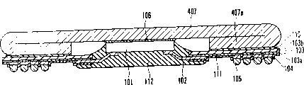
Figure 10 represents the semiconductor device according to fourth embodiment of the invention.Referring to Figure 10, represent with reference marker identical among components identical use and Fig. 1 among Fig. 1, and omitted their detailed description.Figure 10 and 1 difference are that in Figure 10, the peripheral part 407a of radiator 407 bent 180 °, and use crooked peripheral part 407a to form support ring.
Thereby, needn't form special-purpose support ring, and the quantity of element reduced, thereby can provide semiconductor device with low cost.
Manufacturing step below with reference to Figure 11 A and 11B explanation radiator 407.
Shown in Figure 11 A, will be used to form the copper coin (thickness: about 0.2-0.4m) cut into octagon of radiator in advance.Peripheral part 407a bent 180 °, to make square radiator 407, shown in Figure 11 B.
When adopting this example, needn't prepare the element of the special use that is used to form support ring, the quantity of element can correspondingly reduce, with less than the quantity in the conventional example.Because can be only by being bent to form the support ring parts, so manufacturing process is very simple.When the area of the peripheral part 407a of bending was set to be equal to or greater than the area in the zone that will form projected electrode 105, peripheral part 407a can be as supporting when forming projected electrode 105.
When radiator is installed on semiconductor chip 101 and the air that seal together of semiconductor chip 101 expand sometimes, make to encapsulate and break.This problem can solve by following measure.
Figure 12 represents the radiator 407 shown in Figure 10.As shown in figure 12, when forming gap 413 among the peripheral part 407a in bending, sealed air and extraneous air communicate, thereby the air that expands can be released to the outside.
The remodeling of semiconductor device shown in Figure 13-16 expression Figure 10.
In Figure 13, the peripheral part 407a of radiator 407 is bent to such an extent that make their edge surface be with 103 facing to TAB, thereby they have S shape/shape of falling S (becoming digital 5 or 5 shape) cross section.
In Figure 14, the peripheral part 407a of radiator 407 from the state of Figure 11 further to semiconductor chip 101 bendings, thereby they have numeral 9 or fall the cross section of 9 shapes.
In Figure 15, the peripheral part 407a of radiator 407 be bent make their edge surface be in TAB with in the 103 opposite directions, thereby they have the O tee section.
In Figure 16, the peripheral part 407a of radiator 407 is bent to such an extent that make their edge surface sensing TAB be with 103, thereby they have L shaped cross section.At this moment, radiator 407 and TAB fill with potting resin 112 with the interval between 103.
As mentioned above, according to the present invention, radiator and support ring just can be bonded together each other without adhesive.Therefore, can prevent that As time goes on radiator from separating from support ring.
Claims (6)
1. semiconductor device is characterized in that comprising:
Tape carrier (103) by TAB (tape automated bonding) band formation;
Be installed in the semiconductor chip (101) on the described tape carrier;
Metal heat sink (107,207,307) is fixed on the surface of the described semiconductor chip relative with described tape carrier, the heat that the described semiconductor chip that is used for leaving produces, and the shape of described radiator is greater than the shape of described semiconductor chip;
By the footing (407a) that the peripheral part towards the described radiator of described tape carrier bending constitutes, described footing is used to guarantee the predetermined gap between described radiator and the described tape carrier and prevents described tape carrier bending.
2. semiconductor device according to claim 1, wherein said footing is by constituting to the peripheral part of the about 180 ° described radiator of described semiconductor core bending tablet on one side from tape carrier.
3. semiconductor device according to claim 1, wherein said footing is by constituting towards the described peripheral part of described tape carrier bending with described radiator with S shape/tee section of falling S.
4. semiconductor device according to claim 1, wherein said footing is by falling the described peripheral part of described radiator in cross section of 9 shapes and constitute to have numeral 9/ towards described tape carrier bending.
5. semiconductor device according to claim 1, wherein said footing is by constituting towards the described peripheral part of described tape carrier bending with described radiator with O tee section.
6. semiconductor device according to claim 1, wherein said footing is made of a plurality of sweeps that form by the described peripheral part at described radiator, and described adjacent sweep forms gap (413).
Applications Claiming Priority (2)
| Application Number | Priority Date | Filing Date | Title |
|---|---|---|---|
| JP09337510A JP3087709B2 (en) | 1997-12-08 | 1997-12-08 | Semiconductor device and manufacturing method thereof |
| JP337510/1997 | 1997-12-08 |
Related Parent Applications (1)
| Application Number | Title | Priority Date | Filing Date |
|---|---|---|---|
| CN98123317A Division CN1118097C (en) | 1997-12-08 | 1998-12-08 | Semiconductor device and method of manufacturing the same |
Publications (1)
| Publication Number | Publication Date |
|---|---|
| CN1433068A true CN1433068A (en) | 2003-07-30 |
Family
ID=18309342
Family Applications (2)
| Application Number | Title | Priority Date | Filing Date |
|---|---|---|---|
| CN98123317A Expired - Fee Related CN1118097C (en) | 1997-12-08 | 1998-12-08 | Semiconductor device and method of manufacturing the same |
| CN02142701A Pending CN1433068A (en) | 1997-12-08 | 2002-09-18 | Semiconductor device |
Family Applications Before (1)
| Application Number | Title | Priority Date | Filing Date |
|---|---|---|---|
| CN98123317A Expired - Fee Related CN1118097C (en) | 1997-12-08 | 1998-12-08 | Semiconductor device and method of manufacturing the same |
Country Status (5)
| Country | Link |
|---|---|
| US (1) | US5998241A (en) |
| JP (1) | JP3087709B2 (en) |
| KR (1) | KR100342455B1 (en) |
| CN (2) | CN1118097C (en) |
| TW (1) | TW409371B (en) |
Families Citing this family (48)
| Publication number | Priority date | Publication date | Assignee | Title |
|---|---|---|---|---|
| US6323065B1 (en) * | 1997-05-07 | 2001-11-27 | Signetics | Methods for manufacturing ball grid array assembly semiconductor packages |
| US6395582B1 (en) * | 1997-07-14 | 2002-05-28 | Signetics | Methods for forming ground vias in semiconductor packages |
| JPH11204699A (en) * | 1998-01-09 | 1999-07-30 | Sony Corp | Semiconductor device, manufacture thereof and electronic apparatus |
| US6856013B1 (en) * | 1999-02-19 | 2005-02-15 | Micron Technology, Inc. | Integrated circuit packages, ball-grid array integrated circuit packages and methods of packaging an integrated circuit |
| US6160311A (en) * | 1999-06-14 | 2000-12-12 | First International Computer Inc. | Enhanced heat dissipating chip scale package method and devices |
| US6188579B1 (en) * | 1999-07-12 | 2001-02-13 | Lucent Technologies Inc. | Apparatus and methods for forming a printed wiring board assembly to reduce pallet warpage |
| US6825550B2 (en) * | 1999-09-02 | 2004-11-30 | Micron Technology, Inc. | Board-on-chip packages with conductive foil on the chip surface |
| US6329220B1 (en) * | 1999-11-23 | 2001-12-11 | Micron Technology, Inc. | Packages for semiconductor die |
| JP2002033411A (en) * | 2000-07-13 | 2002-01-31 | Nec Corp | Semiconductor device with heat spreader and its manufacturing method |
| US6559537B1 (en) * | 2000-08-31 | 2003-05-06 | Micron Technology, Inc. | Ball grid array packages with thermally conductive containers |
| US7190585B2 (en) * | 2000-09-29 | 2007-03-13 | Intel Corporation | Thermal heat spreaders designed for lower cost manufacturability, lower mass and increased thermal performance |
| WO2002045164A2 (en) * | 2000-12-01 | 2002-06-06 | Broadcom Corporation | Thermally and electrically enhanced ball grid array packaging |
| US20020079572A1 (en) | 2000-12-22 | 2002-06-27 | Khan Reza-Ur Rahman | Enhanced die-up ball grid array and method for making the same |
| US7161239B2 (en) | 2000-12-22 | 2007-01-09 | Broadcom Corporation | Ball grid array package enhanced with a thermal and electrical connector |
| US6906414B2 (en) | 2000-12-22 | 2005-06-14 | Broadcom Corporation | Ball grid array package with patterned stiffener layer |
| US7132744B2 (en) | 2000-12-22 | 2006-11-07 | Broadcom Corporation | Enhanced die-up ball grid array packages and method for making the same |
| US6853070B2 (en) | 2001-02-15 | 2005-02-08 | Broadcom Corporation | Die-down ball grid array package with die-attached heat spreader and method for making the same |
| TW579581B (en) * | 2001-03-21 | 2004-03-11 | Ultratera Corp | Semiconductor device with chip separated from substrate and its manufacturing method |
| US7259448B2 (en) | 2001-05-07 | 2007-08-21 | Broadcom Corporation | Die-up ball grid array package with a heat spreader and method for making the same |
| US6664618B2 (en) * | 2001-05-16 | 2003-12-16 | Oki Electric Industry Co., Ltd. | Tape carrier package having stacked semiconductor elements, and short and long leads |
| JP3651413B2 (en) * | 2001-05-21 | 2005-05-25 | 日立電線株式会社 | Semiconductor device tape carrier, semiconductor device using the same, semiconductor device tape carrier manufacturing method, and semiconductor device manufacturing method |
| US6537848B2 (en) * | 2001-05-30 | 2003-03-25 | St. Assembly Test Services Ltd. | Super thin/super thermal ball grid array package |
| US20030064542A1 (en) * | 2001-10-02 | 2003-04-03 | Corisis David J. | Methods of packaging an integrated circuit |
| US6614658B2 (en) * | 2001-11-05 | 2003-09-02 | International Business Machines Corporation | Flexible cable stiffener for an optical transceiver |
| US6879039B2 (en) * | 2001-12-18 | 2005-04-12 | Broadcom Corporation | Ball grid array package substrates and method of making the same |
| US6861750B2 (en) | 2002-02-01 | 2005-03-01 | Broadcom Corporation | Ball grid array package with multiple interposers |
| US6825108B2 (en) | 2002-02-01 | 2004-11-30 | Broadcom Corporation | Ball grid array package fabrication with IC die support structures |
| US7550845B2 (en) | 2002-02-01 | 2009-06-23 | Broadcom Corporation | Ball grid array package with separated stiffener layer |
| US7245500B2 (en) * | 2002-02-01 | 2007-07-17 | Broadcom Corporation | Ball grid array package with stepped stiffener layer |
| US6876553B2 (en) | 2002-03-21 | 2005-04-05 | Broadcom Corporation | Enhanced die-up ball grid array package with two substrates |
| US7196415B2 (en) | 2002-03-22 | 2007-03-27 | Broadcom Corporation | Low voltage drop and high thermal performance ball grid array package |
| US7482686B2 (en) | 2004-06-21 | 2009-01-27 | Braodcom Corporation | Multipiece apparatus for thermal and electromagnetic interference (EMI) shielding enhancement in die-up array packages and method of making the same |
| US7432586B2 (en) | 2004-06-21 | 2008-10-07 | Broadcom Corporation | Apparatus and method for thermal and electromagnetic interference (EMI) shielding enhancement in die-up array packages |
| US7411281B2 (en) | 2004-06-21 | 2008-08-12 | Broadcom Corporation | Integrated circuit device package having both wire bond and flip-chip interconnections and method of making the same |
| US7786591B2 (en) | 2004-09-29 | 2010-08-31 | Broadcom Corporation | Die down ball grid array package |
| US20070001291A1 (en) * | 2005-06-30 | 2007-01-04 | Infineon Technologies Ag | Anti-warp heat spreader for semiconductor devices |
| CN101546735B (en) * | 2005-08-17 | 2011-08-17 | 南茂科技股份有限公司 | Packaging structure of bug-hole downwards wafer and manufacturing method thereof |
| CN100559561C (en) * | 2005-08-17 | 2009-11-11 | 南茂科技股份有限公司 | Cavity-down chip package and method for manufacturing the same |
| TWI292612B (en) * | 2006-02-27 | 2008-01-11 | Siliconware Precision Industries Co Ltd | Semiconductor package and fabrication method thereof |
| US8183680B2 (en) | 2006-05-16 | 2012-05-22 | Broadcom Corporation | No-lead IC packages having integrated heat spreader for electromagnetic interference (EMI) shielding and thermal enhancement |
| US8575746B2 (en) | 2006-07-20 | 2013-11-05 | Samsung Electronics Co., Ltd. | Chip on flexible printed circuit type semiconductor package |
| CN101221929B (en) * | 2007-01-12 | 2010-05-19 | 日月光半导体制造股份有限公司 | Packaging structure and heat dissipation module thereof |
| US7915727B2 (en) | 2007-07-20 | 2011-03-29 | Samsung Electronics Co., Ltd. | Tape for heat dissipating member, chip on film type semiconductor package including heat dissipating member, and electronic apparatus including the same |
| CN102683299B (en) * | 2011-01-07 | 2015-01-07 | 新电元工业株式会社 | Resin sealing semiconductor device and resin sealing mould |
| US20120188721A1 (en) * | 2011-01-21 | 2012-07-26 | Nxp B.V. | Non-metal stiffener ring for fcbga |
| KR102487563B1 (en) * | 2015-12-31 | 2023-01-13 | 삼성전자주식회사 | Semiconductor package and methods for fabricating the same |
| CN113316842B (en) * | 2019-05-23 | 2023-12-29 | 华为技术有限公司 | Circuit board assembly and electronic equipment |
| US12002795B2 (en) | 2022-04-13 | 2024-06-04 | Google Llc | Pluggable CPU modules with vertical power |
Family Cites Families (15)
| Publication number | Priority date | Publication date | Assignee | Title |
|---|---|---|---|---|
| JPS6333856A (en) * | 1986-07-28 | 1988-02-13 | Furukawa Electric Co Ltd:The | Lead frame for electronic component |
| DE3712654A1 (en) * | 1987-04-14 | 1988-10-27 | Schlafhorst & Co W | METHOD FOR MONITORING THE QUALITY OF PRODUCTION POINTS, YARNS AND SPOOLS ON A MACHINE COMPOSITION FROM AT LEAST A RING SPINDING MACHINE AND AT LEAST A WINDING MACHINE |
| JPH0277148A (en) * | 1988-09-13 | 1990-03-16 | Mitsubishi Electric Corp | Semiconductor device |
| JPH02155256A (en) * | 1988-12-08 | 1990-06-14 | Mitsubishi Electric Corp | Semiconductor device |
| IT1247649B (en) * | 1990-10-31 | 1994-12-28 | Sgs Thomson Microelectronics | RESIN ENCAPSULATION PROCEDURE OF A POWER SEMICONDUCTOR DEVICE MOUNTED ON A HEAT SINK REMOVING THE WIRES FROM THE HEAT SINK THROUGH THE ACTION OF THE COUNTER-MOLD WHEN THE MOLD IS CLOSED |
| KR970005713B1 (en) * | 1992-07-31 | 1997-04-19 | Nec Kk | Process for correcting warped surface of plastic encapsulated semiconductor device |
| US5474957A (en) * | 1994-05-09 | 1995-12-12 | Nec Corporation | Process of mounting tape automated bonded semiconductor chip on printed circuit board through bumps |
| JP2531382B2 (en) * | 1994-05-26 | 1996-09-04 | 日本電気株式会社 | Ball grid array semiconductor device and manufacturing method thereof |
| JPH08274214A (en) * | 1995-03-30 | 1996-10-18 | Seiko Epson Corp | Semiconductor device |
| JP2894254B2 (en) * | 1995-09-20 | 1999-05-24 | ソニー株式会社 | Semiconductor package manufacturing method |
| JP2814966B2 (en) * | 1995-09-29 | 1998-10-27 | 日本電気株式会社 | Semiconductor device |
| JPH09199631A (en) * | 1996-01-23 | 1997-07-31 | Seiko Epson Corp | Structure and manufacturing method of semiconductor device |
| JPH09266265A (en) * | 1996-03-28 | 1997-10-07 | Toshiba Corp | Semiconductor package |
| US5877042A (en) * | 1996-08-28 | 1999-03-02 | Motorola, Inc. | Glass/Metal package and method for producing the same |
| US5909056A (en) * | 1997-06-03 | 1999-06-01 | Lsi Logic Corporation | High performance heat spreader for flip chip packages |
-
1997
- 1997-12-08 JP JP09337510A patent/JP3087709B2/en not_active Expired - Fee Related
-
1998
- 1998-12-07 KR KR1019980053428A patent/KR100342455B1/en not_active IP Right Cessation
- 1998-12-08 US US09/207,557 patent/US5998241A/en not_active Expired - Fee Related
- 1998-12-08 CN CN98123317A patent/CN1118097C/en not_active Expired - Fee Related
- 1998-12-08 TW TW087120404A patent/TW409371B/en not_active IP Right Cessation
-
2002
- 2002-09-18 CN CN02142701A patent/CN1433068A/en active Pending
Also Published As
| Publication number | Publication date |
|---|---|
| CN1219766A (en) | 1999-06-16 |
| KR19990062861A (en) | 1999-07-26 |
| CN1118097C (en) | 2003-08-13 |
| KR100342455B1 (en) | 2002-08-22 |
| JPH11176887A (en) | 1999-07-02 |
| TW409371B (en) | 2000-10-21 |
| US5998241A (en) | 1999-12-07 |
| JP3087709B2 (en) | 2000-09-11 |
Similar Documents
| Publication | Publication Date | Title |
|---|---|---|
| CN1433068A (en) | Semiconductor device | |
| US8021925B2 (en) | Thermal paste containment for semiconductor modules | |
| CN100463125C (en) | Lead frame routed chip pads for semiconductor packages | |
| CN1192041A (en) | Method of manufacturing semiconductor device | |
| CN1647277A (en) | Stacked die half-lead device | |
| CN1215921A (en) | Molded ball grid array type semiconductor device and manufacturing method thereof | |
| CN1550044A (en) | Surface Mountable Optocoupler Preassemblies | |
| CN1160932A (en) | Semiconductor device | |
| CN1320965A (en) | Semiconductor package and mfg. method thereof | |
| JPH06268102A (en) | Resin-sealed semiconductor device | |
| US20140004633A1 (en) | Method for manufacturing led package | |
| KR20120094280A (en) | Light emitting device package and method of fabricating the same | |
| CN1197290A (en) | Semiconductor device | |
| JP2904141B2 (en) | Semiconductor device | |
| CN1220777A (en) | Semiconductor device and method of manufacturing same | |
| EP1560270A2 (en) | Optical device | |
| CN1591850A (en) | Semiconductor package with heat sink | |
| CN1577824A (en) | Method for making a direct chip attach device and structure | |
| CN1868058A (en) | System and method for reducing or eliminating semiconductor device wire sweep | |
| JPS62241355A (en) | semiconductor equipment | |
| CN1256515A (en) | Semiconductor device with grid ball bonded array structure and its manufacturing method | |
| CN220753419U (en) | Integrated circuit package | |
| US20230275008A1 (en) | Semiconductor package with overlapping leads and die pad | |
| US6246109B1 (en) | Semiconductor device and method for fabricating the same | |
| CN1198005A (en) | Semiconductor package and method of manufacturing the same |
Legal Events
| Date | Code | Title | Description |
|---|---|---|---|
| C06 | Publication | ||
| PB01 | Publication | ||
| C10 | Entry into substantive examination | ||
| SE01 | Entry into force of request for substantive examination | ||
| C02 | Deemed withdrawal of patent application after publication (patent law 2001) | ||
| WD01 | Invention patent application deemed withdrawn after publication |