KR102487563B1 - Semiconductor package and methods for fabricating the same - Google Patents
Semiconductor package and methods for fabricating the same Download PDFInfo
- Publication number
- KR102487563B1 KR102487563B1 KR1020150191285A KR20150191285A KR102487563B1 KR 102487563 B1 KR102487563 B1 KR 102487563B1 KR 1020150191285 A KR1020150191285 A KR 1020150191285A KR 20150191285 A KR20150191285 A KR 20150191285A KR 102487563 B1 KR102487563 B1 KR 102487563B1
- Authority
- KR
- South Korea
- Prior art keywords
- semiconductor chip
- dummy substrate
- semiconductor
- mold
- film
- Prior art date
- Legal status (The legal status is an assumption and is not a legal conclusion. Google has not performed a legal analysis and makes no representation as to the accuracy of the status listed.)
- Active
Links
Images


Classifications
-
- H10W70/68—
-
- H10W42/121—
-
- H—ELECTRICITY
- H01—ELECTRIC ELEMENTS
- H01L—SEMICONDUCTOR DEVICES NOT COVERED BY CLASS H10
- H01L23/00—Details of semiconductor or other solid state devices
- H01L23/12—Mountings, e.g. non-detachable insulating substrates
- H01L23/13—Mountings, e.g. non-detachable insulating substrates characterised by the shape
-
- H—ELECTRICITY
- H01—ELECTRIC ELEMENTS
- H01L—SEMICONDUCTOR DEVICES NOT COVERED BY CLASS H10
- H01L21/00—Processes or apparatus adapted for the manufacture or treatment of semiconductor or solid state devices or of parts thereof
- H01L21/02—Manufacture or treatment of semiconductor devices or of parts thereof
- H01L21/04—Manufacture or treatment of semiconductor devices or of parts thereof the devices having potential barriers, e.g. a PN junction, depletion layer or carrier concentration layer
- H01L21/18—Manufacture or treatment of semiconductor devices or of parts thereof the devices having potential barriers, e.g. a PN junction, depletion layer or carrier concentration layer the devices having semiconductor bodies comprising elements of Group IV of the Periodic Table or AIIIBV compounds with or without impurities, e.g. doping materials
- H01L21/30—Treatment of semiconductor bodies using processes or apparatus not provided for in groups H01L21/20 - H01L21/26
- H01L21/302—Treatment of semiconductor bodies using processes or apparatus not provided for in groups H01L21/20 - H01L21/26 to change their surface-physical characteristics or shape, e.g. etching, polishing, cutting
- H01L21/304—Mechanical treatment, e.g. grinding, polishing, cutting
-
- H—ELECTRICITY
- H01—ELECTRIC ELEMENTS
- H01L—SEMICONDUCTOR DEVICES NOT COVERED BY CLASS H10
- H01L21/00—Processes or apparatus adapted for the manufacture or treatment of semiconductor or solid state devices or of parts thereof
- H01L21/02—Manufacture or treatment of semiconductor devices or of parts thereof
- H01L21/04—Manufacture or treatment of semiconductor devices or of parts thereof the devices having potential barriers, e.g. a PN junction, depletion layer or carrier concentration layer
- H01L21/50—Assembly of semiconductor devices using processes or apparatus not provided for in a single one of the groups H01L21/18 - H01L21/326 or H10D48/04 - H10D48/07 e.g. sealing of a cap to a base of a container
- H01L21/56—Encapsulations, e.g. encapsulation layers, coatings
- H01L21/565—Moulds
-
- H—ELECTRICITY
- H01—ELECTRIC ELEMENTS
- H01L—SEMICONDUCTOR DEVICES NOT COVERED BY CLASS H10
- H01L21/00—Processes or apparatus adapted for the manufacture or treatment of semiconductor or solid state devices or of parts thereof
- H01L21/70—Manufacture or treatment of devices consisting of a plurality of solid state components formed in or on a common substrate or of parts thereof; Manufacture of integrated circuit devices or of parts thereof
- H01L21/77—Manufacture or treatment of devices consisting of a plurality of solid state components or integrated circuits formed in, or on, a common substrate
- H01L21/78—Manufacture or treatment of devices consisting of a plurality of solid state components or integrated circuits formed in, or on, a common substrate with subsequent division of the substrate into plural individual devices
-
- H—ELECTRICITY
- H01—ELECTRIC ELEMENTS
- H01L—SEMICONDUCTOR DEVICES NOT COVERED BY CLASS H10
- H01L23/00—Details of semiconductor or other solid state devices
- H01L23/28—Encapsulations, e.g. encapsulating layers, coatings, e.g. for protection
- H01L23/31—Encapsulations, e.g. encapsulating layers, coatings, e.g. for protection characterised by the arrangement or shape
- H01L23/3107—Encapsulations, e.g. encapsulating layers, coatings, e.g. for protection characterised by the arrangement or shape the device being completely enclosed
- H01L23/3135—Double encapsulation or coating and encapsulation
-
- H—ELECTRICITY
- H01—ELECTRIC ELEMENTS
- H01L—SEMICONDUCTOR DEVICES NOT COVERED BY CLASS H10
- H01L23/00—Details of semiconductor or other solid state devices
- H01L23/28—Encapsulations, e.g. encapsulating layers, coatings, e.g. for protection
- H01L23/31—Encapsulations, e.g. encapsulating layers, coatings, e.g. for protection characterised by the arrangement or shape
- H01L23/3157—Partial encapsulation or coating
- H01L23/3164—Partial encapsulation or coating the coating being a foil
-
- H—ELECTRICITY
- H01—ELECTRIC ELEMENTS
- H01L—SEMICONDUCTOR DEVICES NOT COVERED BY CLASS H10
- H01L23/00—Details of semiconductor or other solid state devices
- H01L23/48—Arrangements for conducting electric current to or from the solid state body in operation, e.g. leads, terminal arrangements ; Selection of materials therefor
- H01L23/482—Arrangements for conducting electric current to or from the solid state body in operation, e.g. leads, terminal arrangements ; Selection of materials therefor consisting of lead-in layers inseparably applied to the semiconductor body (electrodes)
- H01L23/4827—Materials
- H01L23/4828—Conductive organic material or pastes, e.g. conductive adhesives, inks
-
- H—ELECTRICITY
- H01—ELECTRIC ELEMENTS
- H01L—SEMICONDUCTOR DEVICES NOT COVERED BY CLASS H10
- H01L23/00—Details of semiconductor or other solid state devices
- H01L23/52—Arrangements for conducting electric current within the device in operation from one component to another, i.e. interconnections, e.g. wires, lead frames
- H01L23/522—Arrangements for conducting electric current within the device in operation from one component to another, i.e. interconnections, e.g. wires, lead frames including external interconnections consisting of a multilayer structure of conductive and insulating layers inseparably formed on the semiconductor body
- H01L23/5221—Crossover interconnections
-
- H—ELECTRICITY
- H01—ELECTRIC ELEMENTS
- H01L—SEMICONDUCTOR DEVICES NOT COVERED BY CLASS H10
- H01L23/00—Details of semiconductor or other solid state devices
- H01L23/52—Arrangements for conducting electric current within the device in operation from one component to another, i.e. interconnections, e.g. wires, lead frames
- H01L23/535—Arrangements for conducting electric current within the device in operation from one component to another, i.e. interconnections, e.g. wires, lead frames including internal interconnections, e.g. cross-under constructions
-
- H—ELECTRICITY
- H01—ELECTRIC ELEMENTS
- H01L—SEMICONDUCTOR DEVICES NOT COVERED BY CLASS H10
- H01L24/00—Arrangements for connecting or disconnecting semiconductor or solid-state bodies; Methods or apparatus related thereto
- H01L24/98—Methods for disconnecting semiconductor or solid-state bodies
-
- H10P95/08—
-
- H10W70/09—
-
- H10W70/60—
-
- H10W70/611—
-
- H10W70/614—
-
- H10W70/65—
-
- H10W72/0198—
-
- H10W74/01—
-
- H10W74/016—
-
- H10W74/10—
-
- H10W74/114—
-
- H10W70/099—
-
- H10W72/073—
-
- H10W72/241—
-
- H10W72/352—
-
- H10W72/874—
-
- H10W72/9413—
-
- H10W74/019—
-
- H10W74/142—
-
- H10W90/734—
-
- H10W90/736—
Landscapes
- Engineering & Computer Science (AREA)
- Microelectronics & Electronic Packaging (AREA)
- Computer Hardware Design (AREA)
- Power Engineering (AREA)
- Physics & Mathematics (AREA)
- Condensed Matter Physics & Semiconductors (AREA)
- General Physics & Mathematics (AREA)
- Manufacturing & Machinery (AREA)
- Structures Or Materials For Encapsulating Or Coating Semiconductor Devices Or Solid State Devices (AREA)
- Internal Circuitry In Semiconductor Integrated Circuit Devices (AREA)
- Geometry (AREA)
- Chemical & Material Sciences (AREA)
- Materials Engineering (AREA)
- Production Of Multi-Layered Print Wiring Board (AREA)
- Dicing (AREA)
Abstract
본 발명은 반도체 패키지 및 그 제조방법에 관한 것으로, 적층체, 상기 적층체의 측면을 둘러싸는 몰드막, 상기 적층체에 전기적으로 연결된 재배선, 그리고 상기 재배선에 전기적으로 연결된 외부단자를 포함한다. 상기 적층체는 활성면과 그 반대면인 비활성면을 갖는 반도체 칩, 상기 반도체 칩의 비활성면 상에 제공된 더미 기판, 그리고 상기 더미 기판과 상기 반도체 칩 사이에 제공되고 상기 더미 기판을 상기 반도체 칩의 비활성면에 접착시키는 접착막을 포함한다. 상기 몰드막은 상기 재배선에 인접한 상면과 그 반대면인 하면을 포함한다. 상기 더미 기판은 상기 몰드막의 하면을 통해 노출된다.The present invention relates to a semiconductor package and a manufacturing method thereof, and includes a laminate, a mold film surrounding a side surface of the laminate, a redistribution electrically connected to the laminate, and an external terminal electrically connected to the redistribution. . The laminate includes a semiconductor chip having an active surface and an inactive surface opposite to the active surface, a dummy substrate provided on the inactive surface of the semiconductor chip, and a dummy substrate provided between the dummy substrate and the semiconductor chip. It includes an adhesive film that adheres to the inactive surface. The mold layer includes an upper surface adjacent to the redistribution and a lower surface opposite to the upper surface. The dummy substrate is exposed through a lower surface of the mold layer.
Description
본 발명은 반도체에 관한 것으로, 보다 구체적으로는 반도체 패키지 및 그 제조방법에 관한 것이다.The present invention relates to a semiconductor, and more particularly, to a semiconductor package and a manufacturing method thereof.
반도체 칩이나 반도체 패키지를 제작하는데 있어서 반도체 칩을 그라인딩하는 공정이 필요할 수 있다. 그라인딩시 반도체 칩에 스크랫치나 크랙이 발생하거나 오염물에 의해 반도체 칩이 오염되면 수율이 하락하게 된다. In manufacturing a semiconductor chip or a semiconductor package, a process of grinding the semiconductor chip may be required. If scratches or cracks are generated in the semiconductor chip during grinding or if the semiconductor chip is contaminated by contaminants, the yield decreases.
본 발명의 목적은 반도체 칩의 손상이나 오염없는 반도체 패키지 및 그 제조방법을 제공함에 있다.An object of the present invention is to provide a semiconductor package without damage or contamination of a semiconductor chip and a manufacturing method thereof.
본 발명의 다른 목적은 수율이 향상된 반도체 패키지 및 그 제조방법을 제공함에 있다.Another object of the present invention is to provide a semiconductor package with improved yield and a manufacturing method thereof.
본 발명의 또 다른 목적은 전기적 내지 기계적 특성이 향상된 반도체 패키지 및 그 제조방법을 제공함에 있다.Another object of the present invention is to provide a semiconductor package with improved electrical or mechanical properties and a manufacturing method thereof.
상기 목적을 달성하기 위한 본 발명에 따른 반도체 패키지 및 그 제조방법은 반도체 칩에 더미 기판을 부착하는 것을 일 특징으로 한다.A semiconductor package and a manufacturing method thereof according to the present invention for achieving the above object are characterized in that a dummy substrate is attached to a semiconductor chip.
상기 특징을 구현할 수 있는 본 발명의 일 실시예에 따른 반도체 패키지는: 적층체; 상기 적층체의 측면을 둘러싸는 몰드막; 상기 적층체에 전기적으로 연결된 재배선; 그리고 상기 재배선에 전기적으로 연결된 외부단자를 포함할 수 있다. 상기 적층체는: 활성면과 그 반대면인 비활성면을 갖는 반도체 칩; 상기 반도체 칩의 비활성면 상에 제공된 더미 기판; 그리고 상기 더미 기판과 상기 반도체 칩 사이에 제공되고, 상기 더미 기판을 상기 반도체 칩의 비활성면에 접착시키는 접착막을 포함할 수 있다. 상기 몰드막은 상기 재배선에 인접한 상면과 그 반대면인 하면을 포함할 수 있다. 상기 더미 기판은 상기 몰드막의 하면을 통해 노출될 수 있다.A semiconductor package according to an embodiment of the present invention capable of implementing the above features includes: a laminate; a mold film surrounding a side surface of the laminate; redistribution electrically connected to the laminate; And it may include an external terminal electrically connected to the redistribution. The laminate includes: a semiconductor chip having an active surface and an inactive surface opposite to the active surface; a dummy substrate provided on an inactive surface of the semiconductor chip; and an adhesive film provided between the dummy substrate and the semiconductor chip and adhering the dummy substrate to an inactive surface of the semiconductor chip. The mold layer may include an upper surface adjacent to the redistribution and a lower surface opposite to the upper surface. The dummy substrate may be exposed through a lower surface of the mold layer.
일 실시예의 반도체 패키지에 있어서, 상기 접착막은 금속 페이스트를 포함할 수 있다.In the semiconductor package of one embodiment, the adhesive layer may include a metal paste.
일 실시예의 반도체 패키지에 있어서, 상기 재배선은 상기 반도체 칩의 활성면 상에 제공되고 그리고 상기 반도체 칩의 측면을 넘어 상기 몰드막 위로 연장될 수 있다.In the semiconductor package of one embodiment, the redistribution may be provided on an active surface of the semiconductor chip and may extend over the mold layer beyond a side surface of the semiconductor chip.
일 실시예의 반도체 패키지에 있어서, 상기 몰드막은 상기 반도체 칩의 측면을 둘러쌀 수 있다. 상기 외부단자는 상기 반도체 칩의 측면을 둘러싸는 상기 몰드막의 상면 상에 제공될 수 있다.In the semiconductor package of one embodiment, the mold layer may surround a side surface of the semiconductor chip. The external terminal may be provided on an upper surface of the mold layer surrounding a side surface of the semiconductor chip.
일 실시예의 반도체 패키지에 있어서, 상기 재배선을 감싸고 그리고 상기 반도체 칩의 활성면과 상기 몰드막의 상면을 덮는 보호막을 더 포함할 수 있다.The semiconductor package of one embodiment may further include a protective layer covering the redistribution and covering an active surface of the semiconductor chip and an upper surface of the mold layer.
일 실시예의 반도체 패키지에 있어서, 상기 더미 기판은 상기 반도체 칩과 동일한 크기를 가질 수 있다.In the semiconductor package of one embodiment, the dummy substrate may have the same size as the semiconductor chip.
일 실시예의 반도체 패키지에 있어서, 상기 더미 기판은 상기 반도체 칩에 비해 크거나 작은 크기를 가질 수 있다.In the semiconductor package of one embodiment, the dummy substrate may have a size larger or smaller than that of the semiconductor chip.
일 실시예의 반도체 패키지에 있어서, 상기 반도체 칩의 활성면은 상기 몰드막의 상면과 공면을 이룰 수 있다.In the semiconductor package according to an exemplary embodiment, an active surface of the semiconductor chip may be coplanar with an upper surface of the mold layer.
상기 특징을 구현할 수 있는 본 발명의 일 실시예에 따른 반도체 패키지는: 반도체 칩과 더미 기판이 금속성 접착막에 의해 접착된 적층체; 상기 적층체의 측면을 감싸고 상면과 그 반대면인 하면을 갖는 몰드막; 및 상기 반도체 칩에 전기적으로 연결되고 상기 몰드막의 상면 상에 제공된 외부단자를 포함할 수 있다. 상기 반도체 칩은 상기 외부단자와 전기적으로 연결되는 회로층이 제공된 활성면과 그 반대면인 비활성면을 포함할 수 있다. 상기 더미 기판은 상기 반도체 칩의 비활성면 상에 제공되고 상기 몰드막의 하면을 통해 노출될 수 있다.A semiconductor package according to an embodiment of the present invention capable of implementing the above characteristics includes: a laminated body in which a semiconductor chip and a dummy substrate are bonded by a metallic adhesive film; a mold film covering a side surface of the laminate and having an upper surface and a lower surface opposite to the upper surface; and an external terminal electrically connected to the semiconductor chip and provided on an upper surface of the mold layer. The semiconductor chip may include an active surface provided with a circuit layer electrically connected to the external terminal and an inactive surface opposite to the active surface. The dummy substrate may be provided on an inactive surface of the semiconductor chip and may be exposed through a lower surface of the mold layer.
일 실시예의 반도체 패키지에 있어서, 상기 반도체 칩의 활성면과 상기 몰드막의 상면을 덮는 보호막을 더 포함할 수 있다.The semiconductor package of one embodiment may further include a protective layer covering an active surface of the semiconductor chip and an upper surface of the mold layer.
일 실시예의 반도체 패키지에 있어서, 상기 외부단자를 상기 반도체 칩의 회로층에 전기적으로 연결하는 재배선을 더 포함할 수 있다. 상기 보호막은 상기 재배선을 감쌀 수 있다.The semiconductor package of one embodiment may further include a redistribution electrically connecting the external terminal to a circuit layer of the semiconductor chip. The passivation layer may cover the redistribution.
일 실시예의 반도체 패키지에 있어서, 상기 반도체 칩은 상기 회로층과 전기적으로 연결된 칩 패드를 더 포함할 수 있다. 상기 재배선은 상기 칩 패드에 접속될 수 있다.In the semiconductor package of one embodiment, the semiconductor chip may further include a chip pad electrically connected to the circuit layer. The redistribution may be connected to the chip pad.
일 실시예의 반도체 패키지에 있어서, 상기 적층체는 상기 몰드막의 두께와 동일한 두께를 가질 수 있다.In the semiconductor package of one embodiment, the laminate may have the same thickness as the mold layer.
일 실시예의 반도체 패키지에 있어서, 상기 금속성 접착막은 구리 페이스트를 포함할 수 있다.In the semiconductor package of one embodiment, the metallic adhesive layer may include copper paste.
상기 특징을 구현할 수 있는 본 발명의 일 실시예에 따른 반도체 패키지의 제조방법은: 더미 기판과 반도체 칩이 접착된 복수개의 적층체들을 제공하고; 상기 적층체들의 측면들을 둘러싸며 상기 더미 기판들을 덮고 그리고 상기 반도체 칩들을 덮지 않는 몰드막을 형성하고; 상기 반도체 칩들에 전기적으로 연결되는 복수개의 재배선들을 형성하고; 상기 재배선들에 전기적으로 연결되고 상기 적층체들의 측면들을 둘러싸는 상기 몰드막 상에 제공되는 복수개의 외부단자들을 형성하고; 상기 몰드막을 그라인딩하여 상기 더미 기판들을 노출시키고; 그리고 상기 그라인딩된 몰드막을 다이싱하여, 상기 적층체가 상기 다이싱된 몰드막으로 둘러싸이고 상기 외부단자가 상기 다이싱된 몰드막 상에 제공된 패키지를 형성하는 것을 포함할 수 있다.A method of manufacturing a semiconductor package according to an embodiment of the present invention capable of implementing the above features includes: providing a plurality of laminates to which a dummy substrate and a semiconductor chip are bonded; forming a mold film surrounding side surfaces of the stacked bodies and covering the dummy substrates and not covering the semiconductor chips; forming a plurality of redistribution wires electrically connected to the semiconductor chips; forming a plurality of external terminals electrically connected to the redistribution lines and provided on the mold film surrounding side surfaces of the stacked bodies; exposing the dummy substrates by grinding the mold layer; and dicing the ground mold film to form a package in which the laminate is surrounded by the diced mold film and the external terminal is provided on the diced mold film.
일 실시예의 제조방법에 있어서, 상기 적층체들을 제공하는 것은: 회로층이 제공된 활성면과 그 반대면인 비활성면을 갖는 반도체 웨이퍼를 제공하고; 상기 반도체 웨이퍼의 비활성면 상에 더미 웨이퍼를 부착하고; 그리고 상기 더미 웨이퍼가 부착된 상기 웨이퍼를 다이싱하여 상기 복수개의 적층체들을 형성하는 것을 포함할 수 있다.In the manufacturing method of an embodiment, providing the stacked bodies includes: providing a semiconductor wafer having an active surface provided with a circuit layer and an inactive surface opposite to the active surface; attaching a dummy wafer on the inactive side of the semiconductor wafer; The method may further include forming the plurality of stacked bodies by dicing the wafer to which the dummy wafer is attached.
일 실시예의 제조방법에 있어서, 상기 더미 웨이퍼를 부착하는 것은: 금속성 접착막을 상기 반도체 웨이퍼의 비활성면과 상기 더미 웨이퍼 사이에 제공하는 것을 포함할 수 있다.In the manufacturing method of an embodiment, attaching the dummy wafer may include providing a metallic adhesive film between the non-active surface of the semiconductor wafer and the dummy wafer.
일 실시예의 제조방법에 있어서, 상기 더미 웨이퍼를 부착하기 이전에, 상기 반도체 웨이퍼의 비활성면을 그라인딩하는 것을 더 포함할 수 있다.The manufacturing method according to an exemplary embodiment may further include grinding an inactive surface of the semiconductor wafer before attaching the dummy wafer.
일 실시예의 제조방법에 있어서, 상기 몰드막을 형성하는 것은: 지지 기판 상에 상기 적층체들을 서로 이격되도록 그리고 상기 반도체 칩들이 상기 지지 기판을 바라보도록 제공하고; 그리고 상기 지지 기판 상에 상기 적층체들을 몰딩하는 상기 몰드막을 형성하는 것을 포함할 수 있다.In the manufacturing method of an embodiment, forming the mold layer may include: providing the stacked bodies on a support substrate to be spaced apart from each other and the semiconductor chips to face the support substrate; The method may further include forming the mold film for molding the laminates on the support substrate.
일 실시예의 제조방법에 있어서, 상기 적층체들을 제공하는 것은: 회로층이 제공된 활성면과 그 반대면인 비활성면을 갖는 반도체 웨이퍼를 제공하고; 상기 웨이퍼를 다이싱하여 복수개의 반도체 칩들로 분리하고; 지지 기판 상에 상기 반도체 칩들을 서로 이격되도록 그리고 상기 반도체 칩들이 상기 지지 기판을 바라보도록 제공하고; 그리고 상기 반도체 칩들 상에 더미 기판들을 부착하는 것을 포함할 수 있다.In the manufacturing method of an embodiment, providing the stacked bodies includes: providing a semiconductor wafer having an active surface provided with a circuit layer and an inactive surface opposite to the active surface; dicing the wafer to separate it into a plurality of semiconductor chips; providing the semiconductor chips on a supporting substrate spaced apart from each other and facing the supporting substrate; And it may include attaching dummy substrates on the semiconductor chips.
일 실시예의 제조방법에 있어서, 상기 웨이퍼를 다이싱하기 이전에, 상기 반도체 웨이퍼의 비활성면을 그라인딩하는 것을 더 포함할 수 있다.The manufacturing method of one embodiment may further include grinding an inactive surface of the semiconductor wafer before dicing the wafer.
일 실시예의 제조방법에 있어서, 상기 더미 기판을 부착하는 것은: 금속성 접착막을 상기 반도체 칩의 비활성면과 상기 더미 기판 사이에 제공하는 것을 포함할 수 있다.In the manufacturing method of an embodiment, attaching the dummy substrate may include providing a metallic adhesive layer between the inactive surface of the semiconductor chip and the dummy substrate.
일 실시예의 제조방법에 있어서, 상기 외부단자를 형성하기 이전에, 상기 반도체 칩과 상기 몰드막 상에 상기 재배선을 감싸는 보호막을 형성하는 것을 더 포함할 수 있다.The manufacturing method of an embodiment may further include forming a protective layer on the semiconductor chip and the mold layer to surround the redistribution before forming the external terminal.
상기 특징을 구현할 수 있는 본 발명의 일 실시예에 따른 반도체 패키지는: 회로층이 제공된 상면 및 그 반대면인 하면을 갖는 반도체 칩; 상기 반도체 칩의 하면을 덮는 보호막: 상기 반도체 칩과 상기 보호막의 측면들을 둘러싸는 몰드막; 상기 반도체 칩의 회로층에 전기적으로 연결되고, 상기 반도체 칩의 상면 상에 제공되고 상기 몰드막 위로 연장된 재배선; 그리고 상기 재배선에 전기적으로 연결되고 상기 반도체 칩의 외곽에 제공된 외부단자를 포함할 수 있다.A semiconductor package according to an embodiment of the present invention capable of implementing the above characteristics includes: a semiconductor chip having an upper surface provided with a circuit layer and a lower surface opposite to the upper surface; A protective film covering the lower surface of the semiconductor chip: a mold film surrounding side surfaces of the semiconductor chip and the protective film; a redistribution electrically connected to a circuit layer of the semiconductor chip, provided on an upper surface of the semiconductor chip, and extending over the mold layer; and an external terminal electrically connected to the redistribution and provided outside the semiconductor chip.
일 실시예의 반도체 패키지에 있어서, 상기 보호막은 상기 반도체 칩의 하면에 접착된 금속 페이스트를 포함할 수 있다.In the semiconductor package of one embodiment, the passivation layer may include a metal paste adhered to a lower surface of the semiconductor chip.
일 실시예의 반도체 패키지에 있어서, 상기 보호막은 상기 금속 페이스트 상에 제공된 더미 기판을 더 포함할 수 있다.In the semiconductor package of one embodiment, the passivation layer may further include a dummy substrate provided on the metal paste.
일 실시예의 반도체 패키지에 있어서, 상기 더미 기판은 상기 반도체 칩과 동일한 크기를 가질 수 있다.In the semiconductor package of one embodiment, the dummy substrate may have the same size as the semiconductor chip.
일 실시예의 반도체 패키지에 있어서, 상기 더미 기판은 상기 반도체 칩에 비해 큰 크기를 가지고, 상기 더미 기판의 측면은 상기 몰드막의 측면에 이르지 않을 수 있다.In the semiconductor package of one embodiment, the dummy substrate may have a larger size than the semiconductor chip, and a side surface of the dummy substrate may not reach a side surface of the mold layer.
일 실시예의 반도체 패키지에 있어서, 상기 더미 기판은 상기 반도체 칩에 비해 작은 크기를 가질 수 있다.In the semiconductor package of one embodiment, the dummy substrate may have a size smaller than that of the semiconductor chip.
본 발명에 의하면, 반도체 칩에 더미 기판을 부착하므로써 반도체 칩의 스크랫치나 크랙 발생을 억제하거나 최소화할 수 있다. 아울러 더미 기판이 반도체 패키지의 휨을 억제하거나 최소화할 수 있다. According to the present invention, by attaching the dummy substrate to the semiconductor chip, it is possible to suppress or minimize the occurrence of scratches or cracks in the semiconductor chip. In addition, the dummy substrate may suppress or minimize warpage of the semiconductor package.
도 1a는 본 발명의 일 실시예에 따른 반도체 패키지를 도시한 단면도이다.
도 1b는 도 1a의 다른 예를 도시한 단면도이다.
도 1c는 도 1a의 또 다른 예를 도시한 단면도이다.
도 1d는 도 1a의 또 다른 예를 도시한 단면도이다.
도 2a 내지 도 2j는 본 발명의 일 실시예에 따른 반도체 패키지의 제조방법을 도시한 단면도들이다.
도 2b는 도 2a의 다른 예를 도시한 단면도이다.
도 2k는 도 2j의 다른 예를 도시한 단면도이다.
도 3a 내지 3f는 본 발명의 일 실시예에 따른 반도체 패키지의 제조방법을 도시한 단면도들이다.
도 3g는 도 3f의 다른 예를 도시한 단면도이다.1A is a cross-sectional view illustrating a semiconductor package according to an exemplary embodiment of the present invention.
Figure 1b is a cross-sectional view showing another example of Figure 1a.
Figure 1c is a cross-sectional view showing another example of Figure 1a.
Figure 1d is a cross-sectional view showing another example of Figure 1a.
2A to 2J are cross-sectional views illustrating a method of manufacturing a semiconductor package according to an embodiment of the present invention.
Figure 2b is a cross-sectional view showing another example of Figure 2a.
Figure 2k is a cross-sectional view showing another example of Figure 2j.
3A to 3F are cross-sectional views illustrating a method of manufacturing a semiconductor package according to an embodiment of the present invention.
Figure 3g is a cross-sectional view showing another example of Figure 3f.
이하, 본 발명에 따른 반도체 패키지 및 그 제조방법을 첨부한 도면을 참조하여 상세히 설명한다.Hereinafter, a semiconductor package and a manufacturing method thereof according to the present invention will be described in detail with reference to the accompanying drawings.
본 발명과 종래 기술과 비교한 이점은 첨부된 도면을 참조한 상세한 설명과 특허청구범위를 통하여 명백하게 될 것이다. 특히, 본 발명은 특허청구범위에서 잘 지적되고 명백하게 청구된다. 그러나, 본 발명은 첨부된 도면과 관련해서 다음의 상세한 설명을 참조함으로써 가장 잘 이해될 수 있다. 도면에 있어서 동일한 참조부호는 다양한 도면을 통해서 동일한 구성요소를 나타낸다.Advantages of the present invention compared to the prior art will become apparent through the detailed description and claims taken with reference to the accompanying drawings. Particularly, the invention is well pointed out and distinctly claimed in the claims. However, the present invention can be best understood by referring to the following detailed description in conjunction with the accompanying drawings. Like reference numerals in the drawings indicate like elements throughout the various drawings.
<반도체 패키지의 일례><An example of a semiconductor package>
도 1a는 본 발명의 일 실시예에 따른 반도체 패키지를 도시한 단면도이다.1A is a cross-sectional view illustrating a semiconductor package according to an exemplary embodiment of the present invention.
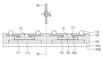
도 1a를 참조하면, 반도체 패키지(1)는 반도체 칩(101)을 포함하는 적층체(10), 반도체 칩(101)과 전기적으로 연결된 재배선(121), 재배선(121)에 전기적으로 연결된 외부단자(125), 그리고 적층체(10)의 측면을 둘러싸는 몰드막(105)을 포함할 수 있다. 일례에 따르면, 반도체 패키지(1)는 인쇄회로기판(PCB)과 같은 패키지 기판을 포함하지 않을 수 있다. Referring to FIG. 1A , a
반도체 칩(101)은 회로층(104)이 형성된 활성면(101a)과 그 반대면인 비활성면(101b)을 가질 수 있다. 활성면(101a)은 회로층(104)과 전기적으로 연결된 하나 혹은 그 이상의 칩 패드들(103)을 포함할 수 있다. 칩 패드들(103)은ㅇ 반도체 칩(101)의 활성면(101a)의 에지에 제공될 수 있댜. 다른 예로, 칩 패드들(103)은 반도체 칩(101)의 활성면(101a)의 센터에 제공될 수 있다. 또 다른 예로, 칩 패드들(103)은 반도체 칩(101)의 활성면(101a)의 전체에 제공될 수 있다. 반도체 칩(101)의 활성면(101a)은 몰드막(105)의 상면(105a)과 공면을 이룰 수 있다. 반도체 칩(101)은 가령 메모리 칩, 로직 칩, 혹은 이들의 조합일 수 있다.The
적층체(10)는 반도체 칩(101)의 비활성면(101c)에 접착막(111)에 의해 부착된 더미 기판(113)을 포함할 수 있다. 접착막(111)과 더미 기판(113) 중 적어도 어느 하나는 전도성 혹은 비전도성 물질을 포함할 수 있다. 일례에 따르면, 접착막(111)은 금속 페이스트(예: 구리 페이스트)를 포함할 수 있고, 더미 기판(113)은 실리콘 기판을 포함할 수 있다. 더미 기판(113)은 몰드막(105)의 하면(105c)을 통해 노출될 수 있다. 적층체(10)의 두께(T2)는 몰드막(105)의 두께(T3)와 동일하거나 유사할 수 있다.The laminate 10 may include a
금속성 접착막(111)은 방열막 역할을 할 수 있으므로, 반도체 칩(101)으로부터의 방열이 효과적일 수 있다. 더미 기판(113)은 도 2i를 참조하여 후술한 바와 같이 제조 공정상 반도체 칩(101)의 스크랫치나 크랙을 방지할 수 있다. 게다가, 더미 기판(113)은 반도체 패키지(1)의 휨(warpage)을 없애거나 최소화할 수 있다. 더미 기판(113)과 반도체 칩(101)은 동일하거나 혹은 서로 다른 크기를 가질 수 있다. 일례로, 더미 기판(113)의 크기(S1)는 반도체 칩(101)의 크기(S2)와 동일하거나 유사할 수 있다. 더미 기판(113)의 두께(X1)와 반도체 칩(101)의 두께(X2)는 동일하거나 다를 수 있다. Since the metallic
재배선(121)은 칩 패드(103)에 전기적으로 연결될 수 있다. 재배선(121)은 반도체 칩(101)의 측면을 넘어 몰드막(105)으로 연장될 수 있다. 외부단자(125)는 재배선(121)의 끝단에 연결될 수 있다. 반도체 패키지(1)는 외부단자(125)가 반도체 칩(101)의 외곽에 제공된 팬-아웃 구조를 가질 수 있다. 보호막(123)은 재배선(121)을 덮으며 반도체 칩(101)의 활성면(101a) 및 몰드막(105)의 상면(105a)을 덮을 수 있다.The
<반도체 패키지의 다른 예들><Other examples of semiconductor packages>
도 1b, 1c 및 1d는 도 1a의 다른 예들을 도시한 단면도들이다. 이하에선 도 1a과 상이한 점에 대해서 상세히 설명하고 동일한 점에 대해선 생략하거나 개략적으로 설명한다.1b, 1c and 1d are cross-sectional views illustrating other examples of FIG. 1a. Hereinafter, different points from those of FIG. 1A will be described in detail, and the same points will be omitted or briefly described.
도 1b를 참조하면, 반도체 패키지(2)는 반도체 칩(101)과 접착막(111)으로 구성된 적층체(10)를 포함할 수 있다. 예컨대, 반도체 패키지(2)는 도 1a의 더미 기판(113)을 포함하지 않을 수 있다. 접착막(111)은 몰드막(105)의 하면(105d)을 통해 노출될 수 있다. 접착막(111)이 금속성인 경우, 접착막(111)은 방열막 역할을 할 수 있고 또한 반도체 패키지(2)의 휨을 억제하는 기판 역할을 할 수 있다.Referring to FIG. 1B , the
도 1c를 참조하면, 반도체 패키지(3)는 반도체 칩(101)의 크기(S2)보다 큰 크기(S1)를 갖는 더미 기판(113)을 포함할 수 있다. 더미 기판(113)은 몰드막(105)의 하면(105c)을 통해 노출될 수 있다. 더미 기판(113)의 측면은 몰드막(105)의 측면에 이르지 않을 수 있다. Referring to FIG. 1C , the
도 1d를 참조하면, 반도체 패키지(4)는 반도체 칩(101)의 크기(S2)보다 작은 크기(S1)를 갖는 더미 기판(113)을 포함할 수 있다. 예컨대, 반도체 패키지(4)의 휨을 억제하거나 최소화하기 위해 더미 기판(113)의 크기(S1)를 반도체 칩(101)의 크기(S1)보다 작게 할 수 있다.Referring to FIG. 1D , the
<반도체 패키지의 제조방법의 일례><An example of a method for manufacturing a semiconductor package>
도 2a 내지 도 2j는 본 발명의 일 실시예에 따른 반도체 패키지의 제조방법을 도시한 단면도들이다. 도 2b는 도 2a의 다른 예를 도시한 단면도이다. 도 2k는 도 2j의 다른 예를 도시한 단면도이다.2A to 2J are cross-sectional views illustrating a method of manufacturing a semiconductor package according to an embodiment of the present invention. Figure 2b is a cross-sectional view showing another example of Figure 2a. Figure 2k is a cross-sectional view showing another example of Figure 2j.
도 2a를 참조하면, 제1 면(102a)과 그 반대면인 제2 면(102b)을 갖는 웨이퍼(102)를 박형화할 수 있다. 웨이퍼(102)는 회로층(104) 그리고 회로층(104)과 전기적으로 연결된 칩 패드들(103)을 포함하는 가령 실리콘 웨이퍼일 수 있다. 웨이퍼(102)의 제2 면(102b)에 대한 그라인딩, 화학기계적 연마, 혹은 에칭 공정으로 웨이퍼(102)를 박형화할 수 있다. 박형화에 의해 제2 면(102b)에 비해 제1 면(102a)에 더 인접한 제3 면(102c)이 드러날 수 있다. Referring to FIG. 2A , a
박형화 공정시 웨이퍼(102)의 용이한 핸들링과 회로층(104)의 보호를 위해 웨이퍼(102)의 제1 면(102a) 상에 가령 DAF(die attach film)와 같은 접착막(72)을 이용하여 지지 기판(70)을 부착할 수 있다. 지지 기판(70)은 웨이퍼(102)와 동일하거나 유사한 크기를 갖는 가령 실리콘 웨이퍼 혹은 유리 기판일 수 있다. 다른 예로, 도 2b에 도시된 것처럼, 웨이퍼(102)의 제1 면(102a)에 보호필름(74)을 부착하여 박형화 공정시 발생할 수 있는 손상이나 오염으로부터 회로층(104)을 보호할 수 있다.For easy handling of the
도 2c를 참조하면, 웨이퍼(102)의 제3 면(102c) 상에 접착막(111)을 이용하여 더미 기판(113)을 부착할 수 있다. 접착막(111)과 더미 기판(113) 중 적어도 어느 하나는 전도성, 비전도성, 혹은 반도체성 물질을 포함할 수 있다. 일례에 따르면, 접착막(111)은 금속 페이스트(예: 구리 페이스트)를 포함할 수 있고, 더미 기판(113)은 실리콘 웨이퍼를 포함할 수 있다. 더미 기판(113)은 웨이퍼(102)와 동일하거나 유사한 크기(예: 직경)를 가질 수 있다. 더미 기판(113)을 부착한 후 웨이퍼(102)로부터 지지 기판(70)과 접착막(72)을 제거할 수 있다.Referring to FIG. 2C , a
도 2d를 참조하면, 스크라이브 레인(90)을 따라 더미 기판(113)이 부착된 웨이퍼(102)를 다이싱할 수 있다. 선택적으로 다이싱 공정시 웨이퍼(102)의 제1 면(102a)에 보호필름(76)을 부착하여 다이싱 공정시 발생할 수 있는 손상이나 오염으로부터 회로층(104)을 보호할 수 있다. 다이싱 공정은 컷팅 장치, 가령 블레이드(95)를 이용할 수 있다. 다른 예로, 레이저 컷팅으로 웨이퍼(102)를 다이싱할 수 있다.Referring to FIG. 2D , the
도 2e를 참조하면, 상기 다이싱에 의해 웨이퍼(102)는 복수개의 적층체들(10)로 분리될 수 있다. 적층체들(10) 각각은 접착막(111)에 의해 더미 기판(113)이 부착된 반도체 칩(101)을 포함할 수 있다. 더미 기판(113)의 크기(S1)는 반도체 칩(101)의 크기(S2)와 동일하거나 유사할 수 있다. 더미 기판(113)의 두께(X1)와 반도체 칩(101)의 두께(X2)는 동일하거나 다를 수 있다. Referring to FIG. 2E , the
반도체 칩(101)은 웨이퍼(102)의 제1 면(102a)에 상당하는 활성면(101a)과 제3 면(102c)에 상당하는 비활성면(101c)을 포함할 수 있다. 반도체 칩(101)은 메모리 칩, 로직 칩, 혹은 이들의 조합일 수 있다.The
도 2f를 참조하면, 지지 기판(80) 상에 가령 DAF(die attach film)과 같은 접착막(82)을 이용하여 복수개의 적층체들(10)을 부착할 수 있다. 지지 기판(80)은 실리콘 웨이퍼 혹은 유리 기판을 포함할 수 있다. 적층체들(10)은 지지 기판(80)의 상면(80a)을 따라 배치될 수 있고 서로 이격될 수 있다. 적층체(10)는 반도체 칩(101)의 활성면(101a)이 지지 기판(80)을 바라보는 상태로 지지 기판(80) 상에 제공될 수 있다. 적층체들(10)의 부착 이후에 지지 기판(80) 상에 적층체들(10)을 덮는 몰드막(105)을 형성할 수 있다. 몰드막(105)은 가령 에폭시 몰딩 컴파운드(EMC)를 포함할 수 있다. Referring to FIG. 2F , a plurality of
도 2g를 참조하면, 적층체들(10)을 몰딩하는 몰드막(105)으로부터 지지 기판(80)과 접착막(82)을 제거할 수 있다. 이에 따라, 적층체들(10)이 노출될 수 있다. 예컨대, 반도체 칩(101)의 활성면(101a)이 드러나게 되어 회로층(104)과 칩 패드(103)가 노출될 수 있다. 반도체 칩(101)의 활성면(101a)은 몰드막(105)의 상면(105a)과 공면을 이룰 수 있다. 몰드막(105)의 두께(T1)는 적층체(10)의 두께(T2)보다 클 수 있다. Referring to FIG. 2G , the
도 2h를 참조하면, 칩 패드(103)에 접속되는 재배선(121)을 형성할 수 있다. 재배선(121)은 반도체 칩(101)의 활성면(101a) 그리고 몰드막(105)을 덮는 보호막(123)으로 덮여질 수 있다. 보호막(123)은 가령 폴리이미드(PI: polyimide), 폴리벤조옥사졸(PBO: polybenzoxazole), 벤조시클로부텐(BCB: benzocyclobutene)과 같은 폴리머를 포함할 수 있다. 다른 예로, 보호막(123)은 실리콘산화막이나 실리콘질화막을 포함할 수 있다. 보호막(123)은 다중막 혹은 단일막일 수 있다. 재배선(121)에 전기적으로 연결되는 솔더볼과 같은 외부단자(125)를 형성할 수 있다. 재배선(121)은 반도체 칩(101)의 측면을 넘어 연장될 수 있다. 외부단자(125)는 반도체 칩(101)의 측면을 넘어 연장된 재배선(121)의 끝단에 인접할 수 있다. 다시 말해, 외부단자(125)는 반도체 칩(101)의 외곽에 배치될 수 있다. Referring to FIG. 2H , a
도 2i를 참조하면, 몰드막(105)의 하면(105b)에 대한 백 그라인딩 공정을 진행할 수 있다. 선택적으로 외부단자(125)를 보호할 수 있는 보호필름(78)이 보호막(123) 상에 부착될 수 있다. 상기 백 그라인딩에 의해 몰드막(105)의 리세스된 하면(105c)을 통해 더미 기판(113)이 드러날 수 있다. 백 그라인딩시 몰드막(105)에 포함된 필러(filler)에 의해 더미 기판(113)에 스크랫치나 크랙이 발생할 수 있다. 반도체 칩(101)은 노출되지 않으므로, 반도체 칩(101)에 스크랫치나 크랙이 발생할 여지가 없을 수 있다. 설령, 더미 기판(113)의 스크랫치나 크랙에 따른 오염물이 발생하더라도, 반도체 칩(101)은 오염물의 침투나 손상으로부터 보호될 수 있다. 그라인딩된 몰드막(105)의 두께(T3)는 적층체(10)의 두께(T2)와 동일하거나 유사할 수 있다.Referring to FIG. 2I , a back grinding process may be performed on the
도 2j를 참조하면, 스크라이브 레인(92)을 따라 몰드막(105)을 다이싱할 수 있다. 다이싱 공정은 컷팅 장치, 가령 블레이드(95)를 이용할 수 있다. 다른 예로, 레이저 컷팅으로 몰드막(105)을 다이싱할 수 있다. 선택적으로 다이싱 공정시 보호막(123)에 보호필름(79)을 부착하여 다이싱 공정시 발생할 수 있는 손상이나 오염으로부터 반도체 칩(101) 내지 외부단자(125)를 보호할 수 있다. 혹은 도 2i의 백 그라인딩 공정시 부착되었던 보호필름(78)을 제거하지 아니하고 다이싱 공정을 진행할 수 있다. 상기 다이싱에 의해 도 1a의 반도체 패키지(1)가 제조될 수 있다.Referring to FIG. 2J , the
도 2k를 참조하면, 몰드막(105)의 하면(105b)에 대한 백 그라인딩 공정시 오버 그라인딩에 의해 더미 기판(113)의 적어도 일부가 제거될 수 있다. 일례로, 오버 그라인딩에 의해 더미 기판(113)이 전부 제거되어 몰드막(105)의 리세스된 하면(105d)을 통해 접착막(111)이 노출될 수 있다. 오버 그라인딩이 발생하더라도, 금속성의 접착막(111)이 크랙 스톱퍼(crack stopper) 내지 그라인딩 스톱퍼(grinding stopper) 역할을 할 수 있다. 이후 몰드막(105)을 다이싱하여 도 1b의 반도체 패키지(2)를 제조할 수 있다.Referring to FIG. 2K , during a back grinding process for the
<반도체 패키지의 제조방법의 일례><An example of a method for manufacturing a semiconductor package>
도 3a 내지 3f는 본 발명의 일 실시예에 따른 반도체 패키지의 제조방법을 도시한 단면도들이다. 도 3g는 도 3f의 다른 예를 도시한 단면도이다.3A to 3F are cross-sectional views illustrating a method of manufacturing a semiconductor package according to an embodiment of the present invention. Figure 3g is a cross-sectional view showing another example of Figure 3f.
도 3a를 참조하면, 제1 면(102a)과 그 반대면인 제2 면(102b) 그리고 회로층(104)과 칩 패드들(103)이 형성된 웨이퍼(102)를 제공할 수 있다. 제2 면(102b)에 대한 그라인딩이나 화학기계적 연마 혹은 에칭 공정으로 웨이퍼(102)를 박형화할 수 있다. 그리고 스크라이브 레인(90)을 따라 웨이퍼(102)를 다이싱할 수 있다. 웨이퍼(102)의 다이싱은 블레이드(95)와 같은 컷팅 장치를 이용할 수 있다. 웨이퍼(102)의 박형화는 도 2a에서와 같이 웨이퍼(102)의 제1 면(102a)에 접착막(72)을 이용하여 지지 기판(70)을 부착하거나, 혹은 도 2b에서와 같이 보호 필름(74)을 부착하여 진행할 수 있다. 웨이퍼(102)의 박형화에 의해 제2 면(102b)에 비해 제1 면(102a)에 더 인접하는 제3 면(102c)이 드러날 수 있다. 웨이퍼(102)의 다이싱은 도 2d에서와 같이 회로층(104)을 보호할 수 있는 보호필름(76)을 부착하여 진행할 수 있다.Referring to FIG. 3A , a
도 3b를 참조하면, 상기 다이싱에 의해 웨이퍼(102)는 복수개의 반도체 칩들(101)로 분리될 수 있다. 반도체 칩(101)은 활성면(101a)과 그 반대면인 비활성면(101c)을 포함할 수 있다. 반도체 칩(101)은 메모리 칩, 로직 칩, 혹은 이들의 조합일 수 있다.Referring to FIG. 3B , the
도 3c를 참조하면, 실리콘 웨이퍼나 유리 기판과 같은 지지 기판(80) 상에 DAF(die attach film)과 같은 접착막(82)을 이용하여 복수개의 반도체 칩들(101)을 부착할 수 있다. 반도체 칩(101)은 그 활성면(101a)이 지지 기판(80)을 바라보는 상태로 지지 기판(80) 상에 제공될 수 있다. 반도체 칩(101)의 비활성면(101c) 상에 접착막(111)을 이용하여 더미 기판(113)을 부착할 수 있다. 이에 따라, 지지 기판(80)의 상면(80a) 상에 서로 이격된 복수개의 적층체들(10)이 제공될 수 있다. 지지 기판(80) 상에 가령 에폭시 몰딩 컴파운드(EMC)를 제공하여 적층체들(10)을 몰딩하는 몰드막(105)을 형성할 수 있다. 일례에 따르면, 접착막(111)은 금속 페이스트(예: 구리 페이스트)를 포함할 수 있고, 더미 기판(113)은 실리콘 웨이퍼를 포함할 수 있다. 더미 기판(113)의 크기(S1)는 반도체 칩(101)의 크기(S2)에 비해 클 수 있다.Referring to FIG. 3C , a plurality of
도 3d를 참조하면, 적층체들(10)을 몰딩하는 몰드막(105)으로부터 지지 기판(80)과 접착막(82)을 제거할 수 있다. 상기 제거에 의해 적층체들(10)이 노출될 수 있다. 가령, 반도체 칩(101)의 활성면(101a)이 드러나게 되어 회로층(104)과 칩 패드(103)가 노출될 수 있다. 반도체 칩(101)의 활성면(101a)은 몰드막(105)의 상면(105a)과 공면을 이룰 수 있다. 몰드막(105)의 두께(T1)는 적층체(10)의 두께(T2)와 동일하거나 더 클 수 있다. 더미 기판(113)의 두께(X1)와 반도체 칩(101)의 두께(X2)는 동일하거나 다를 수 있다. Referring to FIG. 3D , the
도 3e를 참조하면, 칩 패드(103)에 접속되는 재배선(121)을 형성할 수 있고 재배선(121)과 재배선(121)을 덮는 보호막(123)을 형성할 수 있다. 그리고 재배선(121)에 전기적으로 연결되는 솔더볼과 같은 외부단자(125)를 형성할 수 있다. 외부단자(125)는 반도체 칩(101)의 외곽에 배치될 수 있다. Referring to FIG. 3E , a
도 3f를 참조하면, 몰드막(105)의 하면(105b)에 대한 백 그라인딩 공정을 진행할 수 있고, 스크라이브 레인(92)을 따라 몰드막(105)을 다이싱할 수 있다. 백 그라인딩과 다이싱 공정에 의해 도 1c의 반도체 패키지(3)가 제조될 수 있다. 백 그라인딩 공정과 다이싱 중 적어도 어느 하나의 공정을 진행하는 경우, 도 2i에서와 같이 보호필름(78)을 보호막(123) 상에 부착될 수 있다. Referring to FIG. 3F , a back grinding process may be performed on the
도 3g를 참조하면, 더미 기판(113)의 크기(S1)가 반도체 칩(101)의 크기(S2)에 비해 작은 적층체(10)를 형성할 수 있다. 그리고 도 3f에서 전술한 백 그라인딩과 다이싱 공정으로 도 1d의 반도체 패키지(4)를 제조할 수 있다.Referring to FIG. 3G , the
이상의 발명의 상세한 설명은 개시된 실시 상태로 본 발명을 제한하려는 의도가 아니며, 본 발명의 요지를 벗어나지 않는 범위 내에서 다양한 다른 조합, 변경 및 환경에서 사용할 수 있다. 첨부된 청구범위는 다른 실시 상태도 포함하는 것으로 해석되어야 할 것이다.The above detailed description of the invention is not intended to limit the invention to the disclosed embodiments, and can be used in various other combinations, modifications, and environments without departing from the gist of the invention. The appended claims should be construed to cover other embodiments as well.
Claims (20)
상기 적층체의 측면을 둘러싸는 몰드막;
상기 적층체에 전기적으로 연결된 재배선; 그리고
상기 재배선에 전기적으로 연결된 외부단자를 포함하고,
상기 적층체는:
활성면과 그 반대면인 비활성면을 갖는 반도체 칩;
상기 반도체 칩의 비활성면 상에 제공된 더미 기판; 그리고
상기 더미 기판과 상기 반도체 칩 사이에 제공되고, 상기 더미 기판을 상기 반도체 칩의 비활성면에 접착시키는 금속성 접착막을 포함하고,
상기 몰드막은 상기 재배선에 인접한 상면과 그 반대면인 하면을 포함하고,
상기 몰드막은 상기 더미 기판의 일 측면과 직접 접촉하고,
상기 더미 기판은 상기 몰드막의 하면을 통해 노출되고,
상기 더미 기판은 실리콘 웨이퍼를 포함하고,
상기 반도체 칩의 활성면은 상기 몰드막의 상면과 동일한 평면 상에 제공된 반도체 패키지.
laminate;
a mold film surrounding a side surface of the laminate;
redistribution electrically connected to the laminate; And
Including an external terminal electrically connected to the redistribution,
The laminate is:
A semiconductor chip having an active surface and an inactive surface opposite to the active surface;
a dummy substrate provided on an inactive surface of the semiconductor chip; And
a metallic adhesive film provided between the dummy substrate and the semiconductor chip and adhering the dummy substrate to an inactive surface of the semiconductor chip;
The mold film includes an upper surface adjacent to the redistribution and a lower surface opposite to the upper surface,
The mold layer directly contacts one side surface of the dummy substrate;
The dummy substrate is exposed through a lower surface of the mold layer,
The dummy substrate includes a silicon wafer,
An active surface of the semiconductor chip is provided on the same plane as an upper surface of the mold layer.
상기 금속성 접착막은 금속 페이스트를 포함하고,
상기 재배선은 상기 반도체 칩의 활성면 상에 제공되고 그리고 상기 반도체 칩의 측면을 넘어 상기 몰드막 위로 연장된 반도체 패키지.
According to claim 1,
The metallic adhesive film includes a metal paste,
The redistribution is provided on the active surface of the semiconductor chip and extends over the mold layer beyond the side surface of the semiconductor chip.
상기 재배선을 감싸고 그리고 상기 반도체 칩의 활성면과 상기 몰드막의 상면을 덮는 보호막을 더 포함하고,
상기 몰드막은 상기 반도체 칩의 측면을 둘러싸고,
상기 외부단자는 상기 반도체 칩의 측면을 둘러싸는 상기 몰드막의 상면 상에 제공된 반도체 패키지.According to claim 1,
A protective film surrounding the redistribution and covering an active surface of the semiconductor chip and an upper surface of the mold film;
The mold film surrounds a side surface of the semiconductor chip,
The external terminal is provided on the upper surface of the mold layer surrounding the side surface of the semiconductor chip.
상기 더미 기판은 상기 반도체 칩과 동일한 크기를 갖는 반도체 패키지.According to claim 1,
The dummy substrate has the same size as the semiconductor chip semiconductor package.
상기 더미 기판은 상기 반도체 칩에 비해 크거나 작은 크기를 갖는 반도체 패키지.According to claim 1,
The dummy substrate has a size larger or smaller than that of the semiconductor chip.
상기 적층체들의 측면들을 둘러싸며 상기 더미 기판을 덮고 그리고 상기 반도체 칩들을 덮지 않는 몰드막을 형성하고;
상기 반도체 칩들에 전기적으로 연결되는 복수개의 재배선들을 형성하고;
상기 재배선들에 전기적으로 연결되고 상기 적층체들의 측면들을 둘러싸는 상기 몰드막 상에 제공되는 복수개의 외부단자들을 형성하고;
상기 몰드막을 그라인딩하고; 그리고
상기 그라인딩된 몰드막을 다이싱하여, 상기 적층체가 상기 다이싱된 몰드막으로 둘러싸이고 상기 외부단자가 상기 다이싱된 몰드막 상에 제공된 패키지를 형성하는 것을;
포함하고,
상기 더미 기판은 실리콘 웨이퍼를 포함하고,
상기 적층체들을 제공하는 것은 상기 더미 기판 및 상기 반도체 칩 사이에 금속성 접착막을 형성하여, 상기 더미 기판을 상기 금속성 접착막을 통해 상기 반도체 칩에 부착하는 것을 포함하고,
상기 몰드막을 그라인딩하는 것은 상기 더미 기판을 제거하고, 상기 금속성 접착막을 노출시키는 반도체 패키지의 제조방법.
providing a plurality of stacked bodies to which a dummy substrate and a semiconductor chip are bonded;
forming a mold film surrounding side surfaces of the stacked bodies and covering the dummy substrate and not covering the semiconductor chips;
forming a plurality of redistribution wires electrically connected to the semiconductor chips;
forming a plurality of external terminals electrically connected to the redistribution lines and provided on the mold film surrounding side surfaces of the stacked bodies;
grinding the mold film; And
dicing the ground mold film to form a package in which the laminate is surrounded by the diced mold film and the external terminal is provided on the diced mold film;
include,
The dummy substrate includes a silicon wafer,
The providing of the laminates includes forming a metallic adhesive film between the dummy substrate and the semiconductor chip to attach the dummy substrate to the semiconductor chip through the metallic adhesive film;
Grinding the mold film removes the dummy substrate and exposes the metallic adhesive film.
상기 외부단자를 형성하기 이전에, 상기 반도체 칩들과 상기 몰드막 상에 상기 재배선들을 감싸는 보호막을 형성하는 것을 더 포함하고,
상기 적층체들을 제공하는 것은:
회로층이 제공된 활성면과 그 반대면인 비활성면을 갖는 반도체 웨이퍼를 제공하고;
상기 반도체 웨이퍼의 비활성면 상에 더미 웨이퍼를 부착하고; 그리고
상기 더미 웨이퍼가 부착된 상기 웨이퍼를 다이싱하여 상기 복수개의 적층체들을 형성하는 것을 더 포함하고,
상기 몰드막을 형성하는 것은:
지지 기판 상에 상기 적층체들을 서로 이격되도록 그리고 상기 반도체 칩들이 상기 지지 기판을 바라보도록 제공하고; 그리고
상기 지지 기판 상에 상기 적층체들을 몰딩하는 상기 몰드막을 형성하는 것을; 포함하는 반도체 패키지의 제조방법.
According to claim 9,
before forming the external terminal, further comprising forming a protective film on the semiconductor chips and the mold film to surround the redistribution lines;
Providing the laminates are:
providing a semiconductor wafer having an active side provided with a circuit layer and an inactive side opposite to the active side;
attaching a dummy wafer on the inactive side of the semiconductor wafer; And
Further comprising forming the plurality of stacked bodies by dicing the wafer to which the dummy wafer is attached,
Forming the mold film is:
providing the laminates on a support substrate spaced apart from each other and the semiconductor chips facing the support substrate; And
forming the mold film for molding the laminates on the support substrate; A method for manufacturing a semiconductor package comprising:
상기 적층체들을 제공하는 것은:
회로층이 제공된 활성면과 그 반대면인 비활성면을 갖는 반도체 웨이퍼를 제공하고;
상기 반도체 웨이퍼를 다이싱하여 복수개의 반도체 칩들로 분리하고;
지지 기판 상에 상기 반도체 칩들을 서로 이격되도록 그리고 상기 반도체 칩들이 상기 지지 기판을 바라보도록 제공하고; 그리고
상기 반도체 칩들 중 어느 하나 상에 상기 더미 기판을 부착하는 것을;포함하고,
상기 반도체 웨이퍼를 다이싱하기 이전에, 상기 반도체 웨이퍼의 비활성면을 그라인딩하는 것을 더 포함하고,
상기 더미 기판을 부착하는 것은 상기 금속성 접착막을 상기 반도체 칩의 각각의 비활성면과 상기 더미 기판의 사이에 제공하는 것을 포함하는 반도체 패키지의 제조방법.
According to claim 9,
Providing the laminates are:
providing a semiconductor wafer having an active side provided with a circuit layer and an inactive side opposite to the active side;
dicing the semiconductor wafer to separate it into a plurality of semiconductor chips;
providing the semiconductor chips on a supporting substrate spaced apart from each other and facing the supporting substrate; And
attaching the dummy substrate on one of the semiconductor chips;
Further comprising grinding an inactive surface of the semiconductor wafer prior to dicing the semiconductor wafer;
Attaching the dummy substrate includes providing the metallic adhesive film between each inactive surface of the semiconductor chip and the dummy substrate.
상기 반도체 칩의 하면을 덮는 금속성 접착막:
상기 금속성 접착막의 하면 상에 배치된 더미 기판;
상기 반도체 칩과 상기 금속성 접착막의 측면들을 둘러싸는 몰드막;
상기 반도체 칩의 회로층에 전기적으로 연결되고, 상기 반도체 칩의 상면 상에 제공되고 상기 몰드막 위로 연장된 재배선; 그리고
상기 재배선에 전기적으로 연결되고 상기 반도체 칩의 외곽에 제공된 외부단자를;포함하고,
상기 반도체 칩의 측벽은 상기 더미 기판의 제1 측벽과 정렬되고,
상기 몰드막은 상기 더미 기판의 상기 제1 측벽 상에 배치되고,
상기 더미 기판은 실리콘 웨이퍼를 포함하고,
상기 더미 기판은 상기 금속성 접착막을 통해 상기 반도체 칩에 접착되고,
상기 반도체 칩의 상면은 상기 몰드막의 상면과 동일한 평면 상에 제공된 반도체 패키지.
a semiconductor chip having an upper surface provided with a circuit layer and a lower surface opposite to the upper surface;
A metallic adhesive film covering the lower surface of the semiconductor chip:
a dummy substrate disposed on a lower surface of the metallic adhesive film;
a mold layer surrounding side surfaces of the semiconductor chip and the metallic adhesive layer;
a redistribution electrically connected to a circuit layer of the semiconductor chip, provided on an upper surface of the semiconductor chip, and extending over the mold layer; And
An external terminal electrically connected to the redistribution and provided outside the semiconductor chip;
A sidewall of the semiconductor chip is aligned with a first sidewall of the dummy substrate;
the mold layer is disposed on the first sidewall of the dummy substrate;
The dummy substrate includes a silicon wafer,
The dummy substrate is bonded to the semiconductor chip through the metallic adhesive film;
An upper surface of the semiconductor chip is provided on the same plane as an upper surface of the mold layer.
상기 금속성 접착막은 상기 반도체 칩의 하면에 접착된 금속 페이스트를 포함하는 반도체 패키지.According to claim 18,
The metallic adhesive film includes a metal paste adhered to a lower surface of the semiconductor chip.
Priority Applications (3)
| Application Number | Priority Date | Filing Date | Title |
|---|---|---|---|
| KR1020150191285A KR102487563B1 (en) | 2015-12-31 | 2015-12-31 | Semiconductor package and methods for fabricating the same |
| US15/345,779 US9972580B2 (en) | 2015-12-31 | 2016-11-08 | Semiconductor package and method for fabricating the same |
| CN201611144425.5A CN106935556A (en) | 2015-12-31 | 2016-12-13 | Semiconductor package assembly and a manufacturing method thereof |
Applications Claiming Priority (1)
| Application Number | Priority Date | Filing Date | Title |
|---|---|---|---|
| KR1020150191285A KR102487563B1 (en) | 2015-12-31 | 2015-12-31 | Semiconductor package and methods for fabricating the same |
Publications (2)
| Publication Number | Publication Date |
|---|---|
| KR20170080984A KR20170080984A (en) | 2017-07-11 |
| KR102487563B1 true KR102487563B1 (en) | 2023-01-13 |
Family
ID=59235845
Family Applications (1)
| Application Number | Title | Priority Date | Filing Date |
|---|---|---|---|
| KR1020150191285A Active KR102487563B1 (en) | 2015-12-31 | 2015-12-31 | Semiconductor package and methods for fabricating the same |
Country Status (3)
| Country | Link |
|---|---|
| US (1) | US9972580B2 (en) |
| KR (1) | KR102487563B1 (en) |
| CN (1) | CN106935556A (en) |
Families Citing this family (11)
| Publication number | Priority date | Publication date | Assignee | Title |
|---|---|---|---|---|
| WO2018125162A1 (en) * | 2016-12-29 | 2018-07-05 | Intel Corporation | Semiconductor package having passive support wafer |
| KR101963293B1 (en) * | 2017-11-01 | 2019-03-28 | 삼성전기주식회사 | Fan-out semiconductor package |
| US10566261B2 (en) | 2017-11-15 | 2020-02-18 | Taiwan Semiconductor Manufacturing Company, Ltd. | Integrated fan-out packages with embedded heat dissipation structure |
| WO2020000179A1 (en) * | 2018-06-26 | 2020-01-02 | 华为技术有限公司 | Chip packaging structure and chip packaging method |
| KR102536269B1 (en) | 2018-09-14 | 2023-05-25 | 삼성전자주식회사 | semiconductor package and method for manufacturing the same |
| KR102540829B1 (en) * | 2018-10-05 | 2023-06-08 | 삼성전자주식회사 | Semiconductor package, method for semiconductor package and method for re-distribution layer structure |
| US11410902B2 (en) * | 2019-09-16 | 2022-08-09 | Advanced Semiconductor Engineering, Inc. | Semiconductor device package and method of manufacturing the same |
| KR102840201B1 (en) | 2020-03-02 | 2025-07-31 | 삼성전자주식회사 | Semiconductor package |
| KR102635853B1 (en) * | 2020-04-29 | 2024-02-13 | 주식회사 네패스라웨 | Semiconductor package and manufacturing method thereof |
| KR20230025595A (en) * | 2021-08-13 | 2023-02-22 | 삼성전자주식회사 | Semiconductor devices and data storage systems including the same |
| US20240006376A1 (en) * | 2022-07-04 | 2024-01-04 | Intel Corporation | Semiconductor packages for alternate stacked memory and methods of manufacturing the same |
Citations (3)
| Publication number | Priority date | Publication date | Assignee | Title |
|---|---|---|---|---|
| US20140091454A1 (en) | 2012-09-28 | 2014-04-03 | Stats Chippac, Ltd. | Semiconductor Device and Method of Forming Supporting Layer Over Semiconductor Die in Thin Fan-Out Wafer Level Chip Scale Package |
| JP2014192209A (en) * | 2013-03-26 | 2014-10-06 | Tanaka Kikinzoku Kogyo Kk | Semiconductor device and heat dissipation mechanism |
| CN105097726A (en) | 2015-06-16 | 2015-11-25 | 矽力杰半导体技术(杭州)有限公司 | Packaging structure and packaging method |
Family Cites Families (17)
| Publication number | Priority date | Publication date | Assignee | Title |
|---|---|---|---|---|
| JP3087709B2 (en) * | 1997-12-08 | 2000-09-11 | 日本電気株式会社 | Semiconductor device and manufacturing method thereof |
| JP3888302B2 (en) * | 2002-12-24 | 2007-02-28 | カシオ計算機株式会社 | Semiconductor device |
| KR20090061996A (en) | 2007-12-12 | 2009-06-17 | 삼성전자주식회사 | Chip back protection film, manufacturing method thereof and semiconductor package manufacturing method using same |
| KR101055453B1 (en) | 2009-04-10 | 2011-08-08 | 삼성전기주식회사 | Semiconductor package having heat sink and manufacturing method thereof |
| KR101199487B1 (en) | 2009-08-11 | 2012-11-09 | 도레이첨단소재 주식회사 | Thin film process using wafer support adhesive film for processing in semiconductor thin film wafer fabrication |
| KR101159807B1 (en) | 2010-05-07 | 2012-06-26 | (주) 엔지온 | Chip Scale Package of Image Sensor and Manufacturing Method Thereof |
| US8258012B2 (en) * | 2010-05-14 | 2012-09-04 | Stats Chippac, Ltd. | Semiconductor device and method of forming discontinuous ESD protection layers between semiconductor die |
| CN102376590B (en) * | 2010-08-05 | 2013-11-27 | 矽品精密工业股份有限公司 | Chip size package and method for making the same |
| US20120306067A1 (en) * | 2011-06-02 | 2012-12-06 | Taiwan Semiconductor Manufacturing Company, Ltd. | Thermally Enhanced Integrated Circuit Package |
| CN103035578B (en) * | 2011-10-06 | 2017-08-18 | 新科金朋有限公司 | Form the semiconductor devices and method of the reconstructed wafer with compared with larger vector |
| KR101343343B1 (en) * | 2012-01-02 | 2013-12-19 | 한국과학기술원 | 3d stack package of semi-conductor chip and manufacturing method thereof |
| US9000581B2 (en) * | 2012-05-24 | 2015-04-07 | Mediatek Inc. | Semiconductor package |
| US9305854B2 (en) * | 2012-08-21 | 2016-04-05 | Stats Chippac, Ltd. | Semiconductor device and method of forming RDL using UV-cured conductive ink over wafer level package |
| US9559039B2 (en) * | 2012-09-17 | 2017-01-31 | STATS ChipPAC Pte. Ltd. | Semiconductor device and method of using substrate having base and conductive posts to form vertical interconnect structure in embedded die package |
| TWI483365B (en) * | 2012-09-26 | 2015-05-01 | 財團法人工業技術研究院 | Package substrate and its preparation method |
| US9123673B2 (en) | 2013-03-12 | 2015-09-01 | Taiwan Semiconductor Manufacturing Company, Ltd. | Wafer back side processing structure and apparatus |
| KR20150093878A (en) | 2014-02-07 | 2015-08-19 | 앰코 테크놀로지 코리아 주식회사 | Semiconductor package and manufacturing method thereof |
-
2015
- 2015-12-31 KR KR1020150191285A patent/KR102487563B1/en active Active
-
2016
- 2016-11-08 US US15/345,779 patent/US9972580B2/en active Active
- 2016-12-13 CN CN201611144425.5A patent/CN106935556A/en active Pending
Patent Citations (3)
| Publication number | Priority date | Publication date | Assignee | Title |
|---|---|---|---|---|
| US20140091454A1 (en) | 2012-09-28 | 2014-04-03 | Stats Chippac, Ltd. | Semiconductor Device and Method of Forming Supporting Layer Over Semiconductor Die in Thin Fan-Out Wafer Level Chip Scale Package |
| JP2014192209A (en) * | 2013-03-26 | 2014-10-06 | Tanaka Kikinzoku Kogyo Kk | Semiconductor device and heat dissipation mechanism |
| CN105097726A (en) | 2015-06-16 | 2015-11-25 | 矽力杰半导体技术(杭州)有限公司 | Packaging structure and packaging method |
Also Published As
| Publication number | Publication date |
|---|---|
| US9972580B2 (en) | 2018-05-15 |
| CN106935556A (en) | 2017-07-07 |
| KR20170080984A (en) | 2017-07-11 |
| US20170194266A1 (en) | 2017-07-06 |
Similar Documents
| Publication | Publication Date | Title |
|---|---|---|
| KR102487563B1 (en) | Semiconductor package and methods for fabricating the same | |
| US20220384332A1 (en) | Semiconductor structure, package structure, and manufacturing method thereof | |
| US9716080B1 (en) | Thin fan-out multi-chip stacked package structure and manufacturing method thereof | |
| US10090185B2 (en) | Semiconductor device and manufacturing method thereof | |
| US8536672B2 (en) | Image sensor package and fabrication method thereof | |
| US9570314B2 (en) | Methods for singulating semiconductor wafer | |
| US9627368B2 (en) | Semiconductor device using EMC wafer support system and fabricating method thereof | |
| EP3610501B1 (en) | Method of die to wafer bonding of dissimilar thickness die | |
| US9449946B2 (en) | Semiconductor device and manufacturing method thereof | |
| US10332844B2 (en) | Manufacturing method of package structure | |
| US8652939B2 (en) | Method and apparatus for die assembly | |
| US20160322273A1 (en) | Six-sided protection of a wafer-level chip scale package (wlcsp) | |
| KR20180022394A (en) | Method for manufacturing semiconductor package | |
| US10461002B2 (en) | Fabrication method of electronic module | |
| US20180197809A1 (en) | Semiconductor device with frame having arms and related methods | |
| US9449897B2 (en) | Chip package and method for forming the same | |
| KR20150019874A (en) | Semiconductor device and method for manufacturing the same | |
| TWI738923B (en) | Semiconductor structure and manufacturing method thereof | |
| US20160141217A1 (en) | Electronic package and fabrication method thereof | |
| CN100380646C (en) | Semiconductor device and manufacturing method thereof | |
| US9570419B2 (en) | Method of thinning and packaging a semiconductor chip | |
| US20160005653A1 (en) | Flexible wafer-level chip-scale packages with improved board-level reliability | |
| US12266583B2 (en) | Flip chip package unit and associated packaging method | |
| CN106548950A (en) | Method for fabricating IC with stepped sidewalls and related IC device | |
| KR101612220B1 (en) | Method for fabricating semiconductor package and semiconductor package using the same |
Legal Events
| Date | Code | Title | Description |
|---|---|---|---|
| PA0109 | Patent application |
St.27 status event code: A-0-1-A10-A12-nap-PA0109 |
|
| PG1501 | Laying open of application |
St.27 status event code: A-1-1-Q10-Q12-nap-PG1501 |
|
| P22-X000 | Classification modified |
St.27 status event code: A-2-2-P10-P22-nap-X000 |
|
| A201 | Request for examination | ||
| E13-X000 | Pre-grant limitation requested |
St.27 status event code: A-2-3-E10-E13-lim-X000 |
|
| P11-X000 | Amendment of application requested |
St.27 status event code: A-2-2-P10-P11-nap-X000 |
|
| P13-X000 | Application amended |
St.27 status event code: A-2-2-P10-P13-nap-X000 |
|
| PA0201 | Request for examination |
St.27 status event code: A-1-2-D10-D11-exm-PA0201 |
|
| E902 | Notification of reason for refusal | ||
| PE0902 | Notice of grounds for rejection |
St.27 status event code: A-1-2-D10-D21-exm-PE0902 |
|
| P11-X000 | Amendment of application requested |
St.27 status event code: A-2-2-P10-P11-nap-X000 |
|
| P13-X000 | Application amended |
St.27 status event code: A-2-2-P10-P13-nap-X000 |
|
| E90F | Notification of reason for final refusal | ||
| PE0902 | Notice of grounds for rejection |
St.27 status event code: A-1-2-D10-D21-exm-PE0902 |
|
| P11-X000 | Amendment of application requested |
St.27 status event code: A-2-2-P10-P11-nap-X000 |
|
| P13-X000 | Application amended |
St.27 status event code: A-2-2-P10-P13-nap-X000 |
|
| E701 | Decision to grant or registration of patent right | ||
| PE0701 | Decision of registration |
St.27 status event code: A-1-2-D10-D22-exm-PE0701 |
|
| PR0701 | Registration of establishment |
St.27 status event code: A-2-4-F10-F11-exm-PR0701 |
|
| PR1002 | Payment of registration fee |
St.27 status event code: A-2-2-U10-U11-oth-PR1002 Fee payment year number: 1 |
|
| PG1601 | Publication of registration |
St.27 status event code: A-4-4-Q10-Q13-nap-PG1601 |
|
| PR1001 | Payment of annual fee |
St.27 status event code: A-4-4-U10-U11-oth-PR1001 Fee payment year number: 4 |
|
| U11 | Full renewal or maintenance fee paid |
Free format text: ST27 STATUS EVENT CODE: A-4-4-U10-U11-OTH-PR1001 (AS PROVIDED BY THE NATIONAL OFFICE) Year of fee payment: 4 |
|
| P22-X000 | Classification modified |
St.27 status event code: A-4-4-P10-P22-nap-X000 |