CN1178240C - Stached ceramic capacitor and making method thereof - Google Patents
Stached ceramic capacitor and making method thereof Download PDFInfo
- Publication number
- CN1178240C CN1178240C CNB011033355A CN01103335A CN1178240C CN 1178240 C CN1178240 C CN 1178240C CN B011033355 A CNB011033355 A CN B011033355A CN 01103335 A CN01103335 A CN 01103335A CN 1178240 C CN1178240 C CN 1178240C
- Authority
- CN
- China
- Prior art keywords
- ceramic
- layer
- particle
- dielectric matter
- shell structure
- Prior art date
- Legal status (The legal status is an assumption and is not a legal conclusion. Google has not performed a legal analysis and makes no representation as to the accuracy of the status listed.)
- Expired - Lifetime
Links
- 239000003985 ceramic capacitor Substances 0.000 title claims abstract description 34
- 238000000034 method Methods 0.000 title claims description 21
- 239000000919 ceramic Substances 0.000 claims abstract description 111
- 239000002245 particle Substances 0.000 claims abstract description 50
- 239000011258 core-shell material Substances 0.000 claims abstract description 23
- 239000004020 conductor Substances 0.000 claims description 36
- 239000000654 additive Substances 0.000 claims description 21
- 230000000996 additive effect Effects 0.000 claims description 20
- 239000000843 powder Substances 0.000 claims description 19
- 238000004519 manufacturing process Methods 0.000 claims description 11
- 238000005245 sintering Methods 0.000 claims description 11
- 239000000203 mixture Substances 0.000 claims description 10
- 239000000853 adhesive Substances 0.000 claims description 5
- 230000001070 adhesive effect Effects 0.000 claims description 5
- 238000003475 lamination Methods 0.000 claims description 5
- 239000010410 layer Substances 0.000 description 89
- 239000000463 material Substances 0.000 description 6
- 239000000126 substance Substances 0.000 description 4
- 239000007769 metal material Substances 0.000 description 3
- 229910052759 nickel Inorganic materials 0.000 description 3
- 229910052709 silver Inorganic materials 0.000 description 3
- 239000010953 base metal Substances 0.000 description 2
- 230000008602 contraction Effects 0.000 description 2
- 238000002788 crimping Methods 0.000 description 2
- 230000000694 effects Effects 0.000 description 2
- 238000005516 engineering process Methods 0.000 description 2
- 238000010304 firing Methods 0.000 description 2
- 239000011812 mixed powder Substances 0.000 description 2
- 229910052763 palladium Inorganic materials 0.000 description 2
- 208000037656 Respiratory Sounds Diseases 0.000 description 1
- 230000001133 acceleration Effects 0.000 description 1
- 239000002671 adjuvant Substances 0.000 description 1
- 230000003321 amplification Effects 0.000 description 1
- 210000002469 basement membrane Anatomy 0.000 description 1
- 239000003990 capacitor Substances 0.000 description 1
- 210000004027 cell Anatomy 0.000 description 1
- 230000009194 climbing Effects 0.000 description 1
- 239000011248 coating agent Substances 0.000 description 1
- 239000011247 coating layer Substances 0.000 description 1
- 238000000576 coating method Methods 0.000 description 1
- 238000009792 diffusion process Methods 0.000 description 1
- 230000008595 infiltration Effects 0.000 description 1
- 238000001764 infiltration Methods 0.000 description 1
- 229910000510 noble metal Inorganic materials 0.000 description 1
- 238000003199 nucleic acid amplification method Methods 0.000 description 1
- 210000002706 plastid Anatomy 0.000 description 1
- 239000010970 precious metal Substances 0.000 description 1
- 238000007639 printing Methods 0.000 description 1
- 230000001737 promoting effect Effects 0.000 description 1
- 229910052761 rare earth metal Inorganic materials 0.000 description 1
- 238000003756 stirring Methods 0.000 description 1
Images
Classifications
-
- B—PERFORMING OPERATIONS; TRANSPORTING
- B32—LAYERED PRODUCTS
- B32B—LAYERED PRODUCTS, i.e. PRODUCTS BUILT-UP OF STRATA OF FLAT OR NON-FLAT, e.g. CELLULAR OR HONEYCOMB, FORM
- B32B19/00—Layered products comprising a layer of natural mineral fibres or particles, e.g. asbestos, mica
- B32B19/04—Layered products comprising a layer of natural mineral fibres or particles, e.g. asbestos, mica next to another layer of the same or of a different material
-
- H—ELECTRICITY
- H01—ELECTRIC ELEMENTS
- H01G—CAPACITORS; CAPACITORS, RECTIFIERS, DETECTORS, SWITCHING DEVICES, LIGHT-SENSITIVE OR TEMPERATURE-SENSITIVE DEVICES OF THE ELECTROLYTIC TYPE
- H01G4/00—Fixed capacitors; Processes of their manufacture
- H01G4/30—Stacked capacitors
-
- H—ELECTRICITY
- H01—ELECTRIC ELEMENTS
- H01G—CAPACITORS; CAPACITORS, RECTIFIERS, DETECTORS, SWITCHING DEVICES, LIGHT-SENSITIVE OR TEMPERATURE-SENSITIVE DEVICES OF THE ELECTROLYTIC TYPE
- H01G4/00—Fixed capacitors; Processes of their manufacture
- H01G4/002—Details
- H01G4/018—Dielectrics
- H01G4/06—Solid dielectrics
- H01G4/08—Inorganic dielectrics
- H01G4/12—Ceramic dielectrics
- H01G4/1209—Ceramic dielectrics characterised by the ceramic dielectric material
-
- B—PERFORMING OPERATIONS; TRANSPORTING
- B32—LAYERED PRODUCTS
- B32B—LAYERED PRODUCTS, i.e. PRODUCTS BUILT-UP OF STRATA OF FLAT OR NON-FLAT, e.g. CELLULAR OR HONEYCOMB, FORM
- B32B2250/00—Layers arrangement
- B32B2250/03—3 layers
-
- B—PERFORMING OPERATIONS; TRANSPORTING
- B32—LAYERED PRODUCTS
- B32B—LAYERED PRODUCTS, i.e. PRODUCTS BUILT-UP OF STRATA OF FLAT OR NON-FLAT, e.g. CELLULAR OR HONEYCOMB, FORM
- B32B2264/00—Composition or properties of particles which form a particulate layer or are present as additives
- B32B2264/10—Inorganic particles
- B32B2264/107—Ceramic
-
- B—PERFORMING OPERATIONS; TRANSPORTING
- B32—LAYERED PRODUCTS
- B32B—LAYERED PRODUCTS, i.e. PRODUCTS BUILT-UP OF STRATA OF FLAT OR NON-FLAT, e.g. CELLULAR OR HONEYCOMB, FORM
- B32B2311/00—Metals, their alloys or their compounds
- B32B2311/02—Noble metals
- B32B2311/04—Gold
-
- B—PERFORMING OPERATIONS; TRANSPORTING
- B32—LAYERED PRODUCTS
- B32B—LAYERED PRODUCTS, i.e. PRODUCTS BUILT-UP OF STRATA OF FLAT OR NON-FLAT, e.g. CELLULAR OR HONEYCOMB, FORM
- B32B2311/00—Metals, their alloys or their compounds
- B32B2311/02—Noble metals
- B32B2311/09—Palladium
-
- B—PERFORMING OPERATIONS; TRANSPORTING
- B32—LAYERED PRODUCTS
- B32B—LAYERED PRODUCTS, i.e. PRODUCTS BUILT-UP OF STRATA OF FLAT OR NON-FLAT, e.g. CELLULAR OR HONEYCOMB, FORM
- B32B2311/00—Metals, their alloys or their compounds
- B32B2311/22—Nickel or cobalt
-
- B—PERFORMING OPERATIONS; TRANSPORTING
- B32—LAYERED PRODUCTS
- B32B—LAYERED PRODUCTS, i.e. PRODUCTS BUILT-UP OF STRATA OF FLAT OR NON-FLAT, e.g. CELLULAR OR HONEYCOMB, FORM
- B32B2315/00—Other materials containing non-metallic inorganic compounds not provided for in groups B32B2311/00 - B32B2313/04
- B32B2315/02—Ceramics
-
- B—PERFORMING OPERATIONS; TRANSPORTING
- B32—LAYERED PRODUCTS
- B32B—LAYERED PRODUCTS, i.e. PRODUCTS BUILT-UP OF STRATA OF FLAT OR NON-FLAT, e.g. CELLULAR OR HONEYCOMB, FORM
- B32B2457/00—Electrical equipment
- B32B2457/16—Capacitors
-
- Y—GENERAL TAGGING OF NEW TECHNOLOGICAL DEVELOPMENTS; GENERAL TAGGING OF CROSS-SECTIONAL TECHNOLOGIES SPANNING OVER SEVERAL SECTIONS OF THE IPC; TECHNICAL SUBJECTS COVERED BY FORMER USPC CROSS-REFERENCE ART COLLECTIONS [XRACs] AND DIGESTS
- Y10—TECHNICAL SUBJECTS COVERED BY FORMER USPC
- Y10T—TECHNICAL SUBJECTS COVERED BY FORMER US CLASSIFICATION
- Y10T428/00—Stock material or miscellaneous articles
- Y10T428/24—Structurally defined web or sheet [e.g., overall dimension, etc.]
- Y10T428/24942—Structurally defined web or sheet [e.g., overall dimension, etc.] including components having same physical characteristic in differing degree
- Y10T428/2495—Thickness [relative or absolute]
-
- Y—GENERAL TAGGING OF NEW TECHNOLOGICAL DEVELOPMENTS; GENERAL TAGGING OF CROSS-SECTIONAL TECHNOLOGIES SPANNING OVER SEVERAL SECTIONS OF THE IPC; TECHNICAL SUBJECTS COVERED BY FORMER USPC CROSS-REFERENCE ART COLLECTIONS [XRACs] AND DIGESTS
- Y10—TECHNICAL SUBJECTS COVERED BY FORMER USPC
- Y10T—TECHNICAL SUBJECTS COVERED BY FORMER US CLASSIFICATION
- Y10T428/00—Stock material or miscellaneous articles
- Y10T428/25—Web or sheet containing structurally defined element or component and including a second component containing structurally defined particles
- Y10T428/252—Glass or ceramic [i.e., fired or glazed clay, cement, etc.] [porcelain, quartz, etc.]
-
- Y—GENERAL TAGGING OF NEW TECHNOLOGICAL DEVELOPMENTS; GENERAL TAGGING OF CROSS-SECTIONAL TECHNOLOGIES SPANNING OVER SEVERAL SECTIONS OF THE IPC; TECHNICAL SUBJECTS COVERED BY FORMER USPC CROSS-REFERENCE ART COLLECTIONS [XRACs] AND DIGESTS
- Y10—TECHNICAL SUBJECTS COVERED BY FORMER USPC
- Y10T—TECHNICAL SUBJECTS COVERED BY FORMER US CLASSIFICATION
- Y10T428/00—Stock material or miscellaneous articles
- Y10T428/25—Web or sheet containing structurally defined element or component and including a second component containing structurally defined particles
- Y10T428/258—Alkali metal or alkaline earth metal or compound thereof
-
- Y—GENERAL TAGGING OF NEW TECHNOLOGICAL DEVELOPMENTS; GENERAL TAGGING OF CROSS-SECTIONAL TECHNOLOGIES SPANNING OVER SEVERAL SECTIONS OF THE IPC; TECHNICAL SUBJECTS COVERED BY FORMER USPC CROSS-REFERENCE ART COLLECTIONS [XRACs] AND DIGESTS
- Y10—TECHNICAL SUBJECTS COVERED BY FORMER USPC
- Y10T—TECHNICAL SUBJECTS COVERED BY FORMER US CLASSIFICATION
- Y10T428/00—Stock material or miscellaneous articles
- Y10T428/26—Web or sheet containing structurally defined element or component, the element or component having a specified physical dimension
- Y10T428/268—Monolayer with structurally defined element
-
- Y—GENERAL TAGGING OF NEW TECHNOLOGICAL DEVELOPMENTS; GENERAL TAGGING OF CROSS-SECTIONAL TECHNOLOGIES SPANNING OVER SEVERAL SECTIONS OF THE IPC; TECHNICAL SUBJECTS COVERED BY FORMER USPC CROSS-REFERENCE ART COLLECTIONS [XRACs] AND DIGESTS
- Y10—TECHNICAL SUBJECTS COVERED BY FORMER USPC
- Y10T—TECHNICAL SUBJECTS COVERED BY FORMER US CLASSIFICATION
- Y10T428/00—Stock material or miscellaneous articles
- Y10T428/29—Coated or structually defined flake, particle, cell, strand, strand portion, rod, filament, macroscopic fiber or mass thereof
- Y10T428/2982—Particulate matter [e.g., sphere, flake, etc.]
- Y10T428/2991—Coated
- Y10T428/2993—Silicic or refractory material containing [e.g., tungsten oxide, glass, cement, etc.]
- Y10T428/2996—Glass particles or spheres
Landscapes
- Engineering & Computer Science (AREA)
- Power Engineering (AREA)
- Ceramic Engineering (AREA)
- Chemical & Material Sciences (AREA)
- Manufacturing & Machinery (AREA)
- Microelectronics & Electronic Packaging (AREA)
- Inorganic Chemistry (AREA)
- Ceramic Capacitors (AREA)
- Fixed Capacitors And Capacitor Manufacturing Machines (AREA)
Abstract
A multilayer ceramic capacitor comprises dielectric ceramic layers and conductive layers, the dielectric ceramic layers including core-shell structured ceramic particles. The ceramic particles disposed nearer to the conductive layers have shell portions having thickness larger than those of the ceramic particles disposed farther from the conductive layers.
Description
Technical field
The present invention relates to multi-layer ceramic capacitor, particularly the structure of this dielectric substance layer with dielectric substance layer and conductor layer alternative stacked.
Background technology
Multi-layer ceramic capacitor is by following operation manufacturing.At first, make mud.Specifically: at BaTiO
3Deng ceramic dielectric matter powder in add additive and adhesive, by with it with stirrings such as ball mill, mixed number hour, make the suitable mud of viscosity.
Secondly, with for example doctor method, make ceramic green sheet by mud.With this doctor method mud is flowed on basement membrane,, after this, be dried the ceramic green sheet that promptly obtains predetermined thickness by adjusting its thickness with the gap of doctor.
Secondly, on ceramic green sheet, with predetermined pattern coating conductive paste.Then, the sheet that these ceramic green sheets need be used is counted lamination, crimping, make the sheet laminate.After this, the sheet laminate is cut into each assembly of elements size, it is burnt till, make sintered body.Through this firing process, ceramic green sheet burns till and is ceramic dielectric matter layer; Conductive paste burns till and is conductor layer.At last, coating layer is electrically stuck with paste and is burnt till it on this sintered body, forms outer electrode.Use above operation, make multi-layer ceramic capacitor.
There is such problem in such multi-layer ceramic capacitor: promptly prevent the generation of leafing and crackle.Have as one of generation essential factors such as absciss layer: conductive paste and ceramic green sheet shrink the difference of behavior when burning till.For solving this problem, the general technology (just at universalness) of in the conductive paste that forms conductor layer, sneaking into the ceramic dielectric matter that is used to make mud that adopts.Moreover under such purpose, this material of sneaking into conductive paste is called as " material altogether ".
Yet owing to be accompanied by the amount of climbing over a wall greatly and the miniaturization of multi-layer ceramic capacitor in recent years, ceramic dielectric matter layer can not be ignored by the rerum natura variation of ceramic dielectric matter layer due to the diffusion reaction of above-mentioned material altogether to the thin layer development.In addition, also have such problem: when with ceramic dielectric matter layer thin layer, anti-current characteristics worsens.
Summary of the invention
The present invention finishes in view of above purpose, and the object of the invention is to provide the multi-layer ceramic capacitor and the method for making thereof of good and possible big capacity of voltage-resistent characteristic and miniaturization.
In order to reach above-mentioned purpose, the multi-layer ceramic capacitor that is made of ceramic dielectric matter layer and conductor layer alternative stacked has been proposed in the 1st invention, it is characterized in that described ceramic dielectric matter layer contains the ceramic particle of tool core shell structure; Simultaneously, this ceramic particle is from the near more person of conductor layer, and then its housing department is thick more.
According to the present invention, because ceramic dielectric matter layer has following core shell structure, it is bigger than the thickness of its shell portion of the ceramic particle that leaves conductor layer promptly to be in conductor layer ceramic particle nearby, so voltage-resistent characteristic improves.Therefore, the thin layerization by ceramic dielectric matter layer realizes high capacity and miniaturization easily.
Here the core shell structure of so-called ceramic particle be meant as the core of the central part of ceramic particle form physically with shell portion as housing department, chemically different phase structure.
In addition, the whole ceramic particle in the ceramic dielectric matter layer does not just have core shell structure.The scheme that proposes in the 2nd invention of the present invention is characterised in that, when observing with TEM (infiltration type electron microscope), the ratio with the ceramic particle of core shell structure and number of the ceramic particle that does not have core shell structure is 9/1~7/3.
According to the present invention, when improving voltage-resistent characteristic, can also improve dielectric constant.In addition, in the ceramic particle that does not have core shell structure, there are the just particle and the particle that is the shell part of core segment.The just effect of the ceramic particle of core segment performance raising dielectric constant is the effect that shell ceramic particle performance partly improves voltage-resistent characteristic.
The scheme that proposes in the 3rd invention of the present invention is characterised in that do not have the ceramic particle of core shell structure, is present near the interface or conductor layer with conductor layer.
According to the present invention because acceleration of sintering and the ceramic particle that only becomes shell part have good voltage-resistent characteristic, so, since it be present in conductor layer near, thereby can improve all voltage-resistent characteristic of ceramic dielectric matter layer.
In addition, in the 4th invention that the present invention relates to, proposed the manufacture method of multi-layer ceramic capacitor, it is characterized in that it makes the operation of mud by sneak into first additive and adhesive in the first ceramic dielectric matter powder; This mud is processed into sheet, makes the operation of base sheet; Second additive and the second ceramic dielectric matter powder that will contain at least one composition in above-mentioned first additive are mixed into conductive paste, and this conductive paste is coated operation on the base sheet; With a plurality of base sheet laminations, make the operation of laminate and the operation that this laminate is burnt till is formed.
According to the present invention, in sintering process, above-mentioned second additive spreads to the base sheet from conductive paste.This second additive contains at least one composition in the element that forms ceramic dielectric matter layer, in above-mentioned first additive, promotes the growth in conductor layer ceramic particle shell portion nearby.Therefore, have following core shell structure, that is, bigger than the thickness of its shell portion of the ceramic particle that leaves conductor layer at conductor layer ceramic particle nearby.Because its voltage-resistent characteristic of stacked capacitor by manufacturing of the present invention improves, therefore, because the thin layerization of ceramic dielectric matter layer then realizes high capacity and miniaturization easily.
Example as preferred version of the present invention, the scheme that proposes in invention 5 is characterised in that, in the manufacture method of the multi-layer ceramic capacitor described in the invention 4, above-mentioned the 1st dielectric medium powder and the 2nd ceramic dielectric matter powder are same compositions, in addition, in invention 6, the particle diameter of above-mentioned the 2nd ceramic dielectric matter powder is below half of above-mentioned the 1st dielectric medium diameter of particle.
As another preferred version of the present invention, in invention 7, in above-mentioned the 2nd additive, contain the composition of the sintering that promotes the ceramic dielectric layer.
Example as the suitable form of the present invention, propose in invention 3: by the manufacture method of the multi-layer ceramic capacitor of inventing 2 described records, it is characterized in that: the particle diameter of the described second ceramic dielectric matter powder is below half of the described first ceramic dielectric matter diameter of particle.
Description of drawings
Accompanying drawing 1 is the portions cut oblique view of multi-layer ceramic capacitor.
Accompanying drawing 2 is expansion cutaway views of multi-layer ceramic capacitor.
Accompanying drawing 3 is process charts of multi-layer ceramic capacitor.
Being described as follows of symbol:
10... multi-layer ceramic capacitor,
11... the ceramic dielectric layer,
12... conductor layer,
13... laminated body,
14... outer electrode 20,
30... ceramic particle,
21... core,
22... housing department
Embodiment
Describe with reference to the multi-layer ceramic capacitor of accompanying drawing an example involved in the present invention.Accompanying drawing 1 is the portions cut oblique view of multi-layer ceramic capacitor; Accompanying drawing 2 is amplification views of multi-layer ceramic capacitor.
As shown in Figure 1, this multi-layer ceramic capacitor 10 has by ceramic dielectric matter layer 11 and conductor layer 12 alternative stacked to become slightly to be the laminated body 13 of rectangular shape and formed the outer electrode 14 that is connected in described conductor layer 12 at laminated body 13 two ends.Here, the outer electrode 14 at 12 pairs of two ends of conductor layer alternately connects.That is, an end outer electrode 14 alternating floors are connected with conductor layer 12, and other end outer electrode 14 then connects with the conductor layer 12 that different above-mentioned end outer electrodes 14 connect.
Ceramic dielectric matter layer 11 is by for example having BaTiO
3The ceramic sintered bodies that is strong dielectricity constitutes.Conductor layer 12 is made of for example base metal materials such as precious metal material such as Pd, Ag and Ni.Laminated body 13 is with a plurality of laminations of the ceramic green sheet that printed conductive paste, its sintering is formed again.Thus, sintered ceramic base sheet forms ceramic dielectric matter layer 11; The sintering conductive paste forms conductor layer 12.Outer electrode 14 is made of for example metal material such as Ni, Ag.
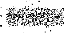
Such as shown in Figure 2, ceramic dielectric matter layer 11 contains the ceramic particle 20 of tool core shell structure and the ceramic particle 30 of no core shell structure.Both compositions are the ceramic particles 20 with core shell structure: the ceramic particle 30 of no core shell structure is about 9: 1~7: 3, in this example about 8: 2.The core shell structure of so-called ceramic particle is such structure: as the core 21 of the central part of ceramic particle be formed on chemically with shell portion 22 as housing department, physically mutually inequality.Again, the ceramic particle 20 with core shell structure is just thick more the closer to 12 its shell portions of conductor layer 22.
Manufacture method with reference to 3 pairs of these multi-layer ceramic capacitors of accompanying drawing is illustrated.Accompanying drawing 3 is process charts of multi-layer ceramic capacitor.
At first, in the first ceramic dielectric plastid powder, sneak into first additive and adhesive, make mud (step S1).Here, use the BaTiO of average grain diameter 0.35 μ m as the first ceramic dielectric matter powder
3Powder.Mainly use the oxide of rare earth element as first additive, specifically use MgO, Ho
2O
3, Sm
2O
3And as the BaSiO of sintering adjuvant
3Mixed powder.Secondly, this mud is made sheet with doctor method etc., obtain ceramic green sheet (step S2).
On the other hand, be made for the conductive paste (step S3) that forms conductor layer.This conductive paste is to be mixed by the metal material powder that base metal constituted, the second ceramic dielectric matter powder and second additives such as noble metals such as Pd, Ag and Ni and adhesive.Here, the metal material powder is the main material that forms conductor layer, and this example uses Ni.
The above-mentioned second ceramic dielectric matter is in order to make the consistent and person of sneaking into of its contraction behavior with ceramic green sheet in sintering process, therefore, and to be advisable with the contraction behavior approximator of the above-mentioned first ceramic dielectric matter.In this example, used with the first ceramic dielectric matter powder and formed and its average grain diameter is half following person by identical.
Above-mentioned second additive is to be used for promoting shell portion to grow up at the ceramic particle of ceramic green sheet.This second additive contains at least one composition in above-mentioned first additive.In this example, MgO, Sm have been used as second additive
2O
3And BaSiO
3Mixed powder.
Secondly, on above-mentioned ceramic green sheet, press predetermined pattern printing conductive paste (step S4), subsequently,, obtain sheet laminate (step S5) this ceramic green sheet lamination, crimping.Secondly, this sheet laminate is cut off by cell size, obtain stacked die (step S6).Once more, the conductive paste of using with outer electrode is coated (step S7) on this stacked die.
Subsequently, under predetermined condition, this stacked die is burnt till (step S8).Here, firing condition is decided according to the composition of ceramic dielectric matter and conductor layer etc.Under this example, in reducing atmosphere gas 1320 ℃ burn till after, change 1000 ℃ N again into
2-O
2Weak oxide atmosphere gas burns till.
At last, outer electrode is electroplated, obtained multi-layer ceramic capacitor 10 (step S9).
According to above step, in the sintering process in above-mentioned steps S8, Low fire ceramic base sheet also forms dielectric substance layer 11; Burn till and form conductor layer 12 being printed in conductive paste on the ceramic green sheet.In this sintering process, second additive that is contained in the conductive paste spreads to ceramic green sheet, and second additive promotes the growth of the ceramic particle housing department on the ceramic green sheet thus.Therefore, nearby there is the thick ceramic particle of housing department 22 in ceramic dielectric matter layer 11 more the closer to conductor layer 12.
Like this, according to the present invention, the ceramic dielectric matter layer 11 of multi-layer ceramic capacitor 10 has such structure: bigger at conductor layer 12 ceramic particle 20 nearby than the thickness of its shell portion 22 of the ceramic particle that leaves conductor layer 12, so voltage-resistent characteristic improves.So can keep good voltage-resistent characteristic, can make ceramic dielectric matter layer 12 thin layerization again, therefore, realize high capacity and miniaturization easily by ceramic dielectric matter layer 12 thin layerization.
Moreover in this example, ceramic dielectric matter layer 11 and conductor layer 12 are to form with 14 while of outer electrode sintering, but the present invention is not so limited.Also promptly, also gained stacked die among the above-mentioned steps S6 can be burnt till.After obtaining sintered body, conductive paste is coated on this sintered body, again it is burnt till, thereby form outer electrode.
Such as previously discussed, according to the present invention, because the ceramic dielectric matter layer of multi-layer ceramic capacitor has such core shell structure, promptly, bigger than its housing department thickness of the ceramic particle that leaves conductor layer at conductor layer ceramic particle nearby, therefore, voltage-resistent characteristic improves.Good voltage-resistent characteristic can be kept, the dielectric substance layer thin layerization can be made again.Therefore, pass through the thin layer realization high capacity and the miniaturization of ceramic dielectric matter layer easily.
Claims (7)
1. multi-layer ceramic capacitor, it is the multi-layer ceramic capacitor that is made of ceramic dielectric matter layer and conductor layer alternative stacked, it is characterized in that: described ceramic dielectric matter layer contains the ceramic particle with core shell structure; Simultaneously, this ceramic particle is from the near more person of conductor layer, and then its housing department is thick more.
2. by the described multi-layer ceramic capacitor of claim 1, it is characterized in that, described ceramic dielectric matter contains ceramic particle with core shell structure and the ceramic particle that does not have core shell structure, with tem observation to the ceramic particle with core shell structure and the number ratio that does not have a ceramic particle of core shell structure be 9/1~7/3.
3. by the described multi-layer ceramic capacitor of claim 2, it is characterized in that, the above-mentioned ceramic particle that does not have core shell structure be present in the interface of conductor layer or conductor layer near.
4. the manufacture method of multi-layer ceramic capacitor is characterized in that having following operation: sneak into the operation that first additive and adhesive are made mud in the first ceramic dielectric matter powder; This mud is processed into sheet, makes the operation of base sheet; Second additive and the second ceramic dielectric matter powder that will contain at least one composition in above-mentioned first additive are mixed into conductive paste, and this conductive paste is coated operation on the base sheet; With a plurality of base sheet laminations, make the operation of laminate and the operation that this laminate is burnt till.
5. by the manufacture method of the described multi-layer ceramic capacitor of claim 4, it is characterized in that above-mentioned first ceramic dielectric matter powder and the above-mentioned second ceramic dielectric matter powder are same compositions.
6. according to the manufacture method of claim 4 or 5 described multi-layer ceramic capacitors, it is characterized in that: the particle diameter of the described second ceramic dielectric matter powder is below half of the described first dielectric medium diameter of particle.
7. by the manufacture method of the described multi-layer ceramic capacitor of claim 4, it is characterized in that above-mentioned second additive contains the composition of the sintering that promotes ceramic dielectric matter layer.
Applications Claiming Priority (2)
| Application Number | Priority Date | Filing Date | Title |
|---|---|---|---|
| JP2000026461 | 2000-02-03 | ||
| JP26461/2000 | 2000-02-03 |
Publications (2)
| Publication Number | Publication Date |
|---|---|
| CN1316752A CN1316752A (en) | 2001-10-10 |
| CN1178240C true CN1178240C (en) | 2004-12-01 |
Family
ID=18552191
Family Applications (1)
| Application Number | Title | Priority Date | Filing Date |
|---|---|---|---|
| CNB011033355A Expired - Lifetime CN1178240C (en) | 2000-02-03 | 2001-01-31 | Stached ceramic capacitor and making method thereof |
Country Status (5)
| Country | Link |
|---|---|
| US (1) | US6514603B2 (en) |
| KR (1) | KR100771757B1 (en) |
| CN (1) | CN1178240C (en) |
| HK (1) | HK1039210A1 (en) |
| MY (1) | MY122833A (en) |
Families Citing this family (17)
| Publication number | Priority date | Publication date | Assignee | Title |
|---|---|---|---|---|
| US6780494B2 (en) * | 2002-03-07 | 2004-08-24 | Tdk Corporation | Ceramic electronic device and method of production of same |
| JP2005159224A (en) * | 2003-11-28 | 2005-06-16 | Tdk Corp | Laminated ceramic capacitor |
| KR100649580B1 (en) * | 2003-12-15 | 2006-11-28 | 삼성전기주식회사 | Method for Manufacturing Multilayered Ceramic Capacitor by Spin Coating and Multilayered Ceramic Capacitor |
| KR100755685B1 (en) * | 2004-12-16 | 2007-09-05 | 삼성전자주식회사 | Thin Film Capacitor and Manufacturing Method of Thin Film Capacitor |
| JP2006319205A (en) * | 2005-05-13 | 2006-11-24 | Taiyo Yuden Co Ltd | Laminated ceramic capacitor and its manufacturing method |
| WO2010023575A1 (en) * | 2008-08-26 | 2010-03-04 | Nxp B.V. | A capacitor and a method of manufacturing the same |
| JP5321001B2 (en) * | 2008-11-17 | 2013-10-23 | 富士通株式会社 | Structure, capacitor, and method of manufacturing capacitor |
| JP4992918B2 (en) * | 2009-01-30 | 2012-08-08 | 株式会社村田製作所 | Dielectric ceramic and multilayer ceramic capacitors |
| US8561271B2 (en) | 2009-12-16 | 2013-10-22 | Liang Chai | Methods for manufacture a capacitor with three-dimensional high surface area electrodes |
| DE102010035488B4 (en) * | 2010-08-26 | 2018-11-15 | Snaptrack, Inc. | Production of ceramic green films and their use for the production of ceramics |
| KR20140001896A (en) | 2010-10-12 | 2014-01-07 | 애프리콧 머티어리얼즈 테크놀로지스, 엘엘씨 | Ceramic capacitor and methods of manufacture |
| KR101872520B1 (en) * | 2011-07-28 | 2018-06-29 | 삼성전기주식회사 | Laminated ceramic electronic parts |
| JP5189705B1 (en) * | 2012-09-25 | 2013-04-24 | 田中貴金属工業株式会社 | Sensor electrode, manufacturing method thereof, and metal paste for electrode formation |
| CN106032326B (en) * | 2015-03-20 | 2020-12-01 | 深圳光启高等理工研究院 | Multilayer composite ceramic plate and preparation method thereof |
| US10332684B2 (en) * | 2015-07-19 | 2019-06-25 | Vq Research, Inc. | Methods and systems for material cladding of multilayer ceramic capacitors |
| US10431508B2 (en) | 2015-07-19 | 2019-10-01 | Vq Research, Inc. | Methods and systems to improve printed electrical components and for integration in circuits |
| WO2021171920A1 (en) * | 2020-02-27 | 2021-09-02 | 京セラ株式会社 | Capacitor |
Family Cites Families (12)
| Publication number | Priority date | Publication date | Assignee | Title |
|---|---|---|---|---|
| JPH02251122A (en) * | 1989-03-24 | 1990-10-08 | Taiyo Yuden Co Ltd | Conductive paste for electrode of ceramic capacitor |
| JPH07118431B2 (en) * | 1991-03-16 | 1995-12-18 | 太陽誘電株式会社 | Porcelain capacitor and method of manufacturing the same |
| US6160472A (en) * | 1995-03-24 | 2000-12-12 | Tdk Corporation | Multilayer varistor |
| JP3391269B2 (en) * | 1998-01-20 | 2003-03-31 | 株式会社村田製作所 | Dielectric ceramic and its manufacturing method, and multilayer ceramic electronic component and its manufacturing method |
| JP3391268B2 (en) * | 1998-01-20 | 2003-03-31 | 株式会社村田製作所 | Dielectric ceramic and its manufacturing method, and multilayer ceramic electronic component and its manufacturing method |
| JP3514117B2 (en) * | 1998-06-03 | 2004-03-31 | 株式会社村田製作所 | Multilayer ceramic electronic component, method of manufacturing multilayer ceramic electronic component, and conductive paste for forming internal electrode |
| US6243254B1 (en) * | 1998-08-11 | 2001-06-05 | Murata Manufacturing Co., Ltd. | Dielectric ceramic composition and laminated ceramic capacitor using the same |
| JP2000223351A (en) * | 1999-01-28 | 2000-08-11 | Murata Mfg Co Ltd | Multilayer ceramic capable |
| JP3376963B2 (en) * | 1999-06-30 | 2003-02-17 | 株式会社村田製作所 | Multilayer ceramic capacitor and method of manufacturing the same |
| JP3827901B2 (en) * | 1999-12-24 | 2006-09-27 | 太陽誘電株式会社 | Multilayer ceramic capacitor |
| JP2001185437A (en) * | 1999-12-24 | 2001-07-06 | Taiyo Yuden Co Ltd | Laminated ceramic capacitor |
| JP2001240466A (en) * | 2000-02-28 | 2001-09-04 | Taiyo Yuden Co Ltd | Porcelain of dielectrics and electronic parts of laminated ceramics |
-
2001
- 2001-01-31 CN CNB011033355A patent/CN1178240C/en not_active Expired - Lifetime
- 2001-02-01 KR KR1020010004880A patent/KR100771757B1/en active IP Right Grant
- 2001-02-02 MY MYPI20010461A patent/MY122833A/en unknown
- 2001-02-02 US US09/775,696 patent/US6514603B2/en not_active Expired - Lifetime
-
2002
- 2002-01-28 HK HK02100644A patent/HK1039210A1/en not_active IP Right Cessation
Also Published As
| Publication number | Publication date |
|---|---|
| CN1316752A (en) | 2001-10-10 |
| HK1039210A1 (en) | 2002-04-12 |
| KR100771757B1 (en) | 2007-10-30 |
| US6514603B2 (en) | 2003-02-04 |
| US20010012561A1 (en) | 2001-08-09 |
| KR20010078253A (en) | 2001-08-20 |
| MY122833A (en) | 2006-05-31 |
Similar Documents
| Publication | Publication Date | Title |
|---|---|---|
| CN1178240C (en) | Stached ceramic capacitor and making method thereof | |
| KR101771728B1 (en) | Laminated ceramic electronic parts and fabricating method thereof | |
| CN1183561C (en) | Stacked ceramic capacitor and mfg. method thereof | |
| KR20010051240A (en) | Monolithic ceramic electronic component and method for making the same | |
| JP5904305B2 (en) | Multilayer ceramic capacitor and manufacturing method thereof | |
| KR20060105585A (en) | Laminated Ceramic Electronic Components and Manufacturing Method Thereof | |
| CN1090375C (en) | Monolithic ceramic capacitor and production method thereof | |
| JP3350949B2 (en) | Conductive paste | |
| JP2004345927A (en) | Method for manufacturing irreducible dielectric ceramic, irreducible dielectric ceramic, and laminated ceramic capacitor | |
| JP5452244B2 (en) | Multilayer ceramic electronic component and manufacturing method thereof | |
| JP5925628B2 (en) | Multilayer ceramic electronic component and manufacturing method thereof | |
| JP2012182355A (en) | Multilayer ceramic capacitor and manufacturing method of multilayer ceramic capacitor | |
| JP2000340450A (en) | Laminated ceramic capacitor and manufacture thereof | |
| JP3514117B2 (en) | Multilayer ceramic electronic component, method of manufacturing multilayer ceramic electronic component, and conductive paste for forming internal electrode | |
| JP2012195557A (en) | Electrode sintered body, laminated electronic component, internal electrode paste, manufacturing method of electrode sintered body, and manufacturing method of laminated electronic component | |
| JP4048887B2 (en) | Multilayer ceramic electronic components | |
| JP4816202B2 (en) | Conductive paste and method for manufacturing ceramic electronic component | |
| JP3793697B2 (en) | Multilayer ceramic capacitor and manufacturing method thereof | |
| CN110808165B (en) | Multilayer ceramic electronic component and method for manufacturing the same | |
| JP2010212503A (en) | Laminated ceramic capacitor | |
| CN1211316C (en) | Dielectric ceramic material, preparation method thereof and method for producing ceramic capacitor | |
| US20010056028A1 (en) | Dielectric ceramic composition, ceramic capacitor using the composition and method of producing thereof | |
| CN116417255A (en) | Multilayer electronic component | |
| JP4076393B2 (en) | Conductive paste and electronic components | |
| JPH1092226A (en) | Conductive composition |
Legal Events
| Date | Code | Title | Description |
|---|---|---|---|
| C06 | Publication | ||
| PB01 | Publication | ||
| C10 | Entry into substantive examination | ||
| SE01 | Entry into force of request for substantive examination | ||
| C10 | Entry into substantive examination | ||
| SE01 | Entry into force of request for substantive examination | ||
| C14 | Grant of patent or utility model | ||
| GR01 | Patent grant | ||
| CX01 | Expiry of patent term |
Granted publication date: 20041201 |
|
| CX01 | Expiry of patent term |