[go: up one dir, main page]

CN113169151A - Interconnect structure - Google Patents

Interconnect structure Download PDF

Info

Publication number
CN113169151A
CN113169151A CN201980077502.5A CN201980077502A CN113169151A CN 113169151 A CN113169151 A CN 113169151A CN 201980077502 A CN201980077502 A CN 201980077502A CN 113169151 A CN113169151 A CN 113169151A
Authority
CN
China
Prior art keywords
conductive interconnect
substrate
interconnect structure
microelectronic assembly
conductive
Prior art date
Legal status (The legal status is an assumption and is not a legal conclusion. Google has not performed a legal analysis and makes no representation as to the accuracy of the status listed.)
Granted
Application number
CN201980077502.5A
Other languages
Chinese (zh)
Other versions
CN113169151B (en
Inventor
C·E·尤佐
G·G·小方丹
J·A·泰尔
Current Assignee (The listed assignees may be inaccurate. Google has not performed a legal analysis and makes no representation or warranty as to the accuracy of the list.)
Insulation Semiconductor Bonding Technology Co
Original Assignee
Evanss Adhesive Technologies
Priority date (The priority date is an assumption and is not a legal conclusion. Google has not performed a legal analysis and makes no representation as to the accuracy of the date listed.)
Filing date
Publication date
Application filed by Evanss Adhesive Technologies filed Critical Evanss Adhesive Technologies
Publication of CN113169151A publication Critical patent/CN113169151A/en
Application granted granted Critical
Publication of CN113169151B publication Critical patent/CN113169151B/en
Active legal-status Critical Current
Anticipated expiration legal-status Critical

Links

Images

Classifications

    • H10W20/062
    • H10W20/42
    • H10W20/40
    • H10P95/90
    • H10W20/023
    • H10W20/0245
    • H10W20/0261
    • H10W20/056
    • H10W20/0698
    • H10W20/074
    • H10W20/077
    • H10W20/20
    • H10W20/2125
    • H10W20/216
    • H10W20/43
    • H10W70/60
    • H10W72/013
    • H10W72/30
    • H10W74/134
    • H10W74/481
    • H10W72/019
    • H10W72/01935
    • H10W72/01951
    • H10W72/0198
    • H10W72/90
    • H10W72/921
    • H10W72/923
    • H10W72/926
    • H10W72/931
    • H10W72/934
    • H10W72/941
    • H10W72/951
    • H10W72/952
    • H10W72/953
    • H10W80/037
    • H10W80/312
    • H10W80/327
    • H10W80/732
    • H10W90/792

Landscapes

  • Engineering & Computer Science (AREA)
  • Computer Hardware Design (AREA)
  • Microelectronics & Electronic Packaging (AREA)
  • Power Engineering (AREA)
  • Physics & Mathematics (AREA)
  • Condensed Matter Physics & Semiconductors (AREA)
  • General Physics & Mathematics (AREA)
  • Internal Circuitry In Semiconductor Integrated Circuit Devices (AREA)
  • Manufacturing & Machinery (AREA)
  • Geometry (AREA)

Abstract

包括工艺步骤的代表性技术和设备可以被采用,以减轻导电互连结构中的不期望的凹陷和电介质键合表面的腐蚀。例如,嵌入层可以被添加到凹陷或腐蚀的表面上,以消除不需要的凹陷或空隙并且形成平坦的键合表面。包括工艺步骤的附加技术和设备可以被采用,以在导电互连结构中形成期望的开口,其中开口相对于互连结构的导电材料的体积可以具有预先确定的或期望的体积。这些技术、设备和工艺中的每个可以在经键合的裸片和晶片的键合表面处提供对更大直径、更大体积或混合尺寸的导电互连结构的使用。

Figure 201980077502

Representative techniques and equipment, including process steps, may be employed to mitigate undesired recesses in conductive interconnect structures and corrosion of dielectric bonding surfaces. For example, an inlay layer can be added to a recessed or etched surface to eliminate unwanted recesses or voids and create a flat bonding surface. Additional techniques and equipment, including process steps, may be employed to form desired openings in the conductive interconnect structure, wherein the opening may have a predetermined or desired volume relative to the volume of conductive material of the interconnect structure. Each of these techniques, apparatus, and processes may provide for the use of larger diameter, larger volume, or mixed size conductive interconnect structures at the bonding surfaces of bonded dies and wafers.

Figure 201980077502

Description

Interconnect structure
Cross reference to priority claims and related applications
This application claims benefit of U.S. non-provisional application No. 16/657,696 filed on day 10/18 in 2019, and is also entitled to priority from 35 u.s.c. § 119(e) (1) U.S. provisional application No. 62/748,653 filed on day 10/22 in 2018, and U.S. provisional application No. 62/902,207 filed on day 09/18 in 2019, both of which are incorporated herein by reference in their entireties.
Technical Field
The following description relates to integrated circuits ("ICs"). More particularly, the following description relates to the fabrication of IC dies and wafers.
Background
Microelectronic elements typically include thin plates of semiconductor materials, such as silicon or gallium arsenide, which are commonly referred to as semiconductor wafers. The wafer may be formed to include a plurality of integrated chips or dies on the wafer surface and/or partially embedded within the wafer. The die, which is separate from the wafer, is typically provided as a separate pre-packaged unit. In some package designs, the die is mounted to a substrate or chip carrier, which in turn is mounted on a circuit panel such as a Printed Circuit Board (PCB). For example, many die are provided in packages suitable for surface mounting.
The packaged semiconductor dies may also be provided in a "stacked" arrangement, where one package is provided, for example, on a circuit board or other carrier, and the other package is mounted over the first package. These arrangements may allow multiple different dies and devices to be mounted within a single footprint on a circuit board, and may further facilitate high speed operation by providing short interconnections between packages. Typically, the interconnect distance may be only slightly greater than the thickness of the die itself. To achieve interconnections within the stack of die packages, interconnect structures for mechanical and electrical connections may be provided on both sides (e.g., faces) of each die package (except for the topmost package).
Further, the die or wafers may be stacked in a three-dimensional arrangement as part of various microelectronic packaging schemes. This may include stacking layers of one or more dies, devices, and/or wafers on a larger base die, device, wafer, substrate, etc., stacking multiple dies or wafers in a vertical or horizontal arrangement, and various combinations of the two.
The die or wafer may be bonded in a stacked arrangement using a variety of bonding techniques, including direct dielectric bonding, non-adhesive techniques (such as,
Figure BDA0003082427780000021
) Or a hybrid bonding technique (such as,
Figure BDA0003082427780000022
) Both are available from Invensas binding Technologies, Inc. (formerly Ziptronix, Inc.) of Xperi corporation. Bonding includes spontaneous processes that occur under ambient conditions when two prepared surfaces are brought together (see, e.g., U.S. patent nos. 6864585 and 7485968, incorporated herein in their entireties).
When bonding stacked dies using direct bonding techniques, it is often desirable that the surface of the die to be bonded be extremely flat and smooth. For example, in general, these surfaces should have very low variation in surface topography (i.e., nanoscale variation) so that the surfaces can be mated to form a durable bond. One or more of the bonding surfaces of the die or wafer are typically planarized using Chemical Mechanical Polishing (CMP) or the like to achieve the extremely flat and smooth surface required for bonding.
The respective mating surfaces of the dies or wafers to be bonded (which may comprise silicon or another suitable material) typically include conductive interconnect structures (which may be metal) embedded within an inorganic dielectric layer (e.g., such as an oxide, nitride, oxynitride, oxycarbide, carbide, carbonitride, diamond-like material, glass, ceramic, glass-ceramic, etc.) at the bonding surfaces.
The conductive interconnect structures may be formed by, for example, damascene techniques and may include structures having varying widths and dimensions. The conductive interconnect structures may be arranged and aligned at the bonding surface such that the conductive interconnect structures from the respective die surfaces are bonded during bonding. The bonded interconnect structure forms a continuous conductive interconnect (for signal, power, thermal transfer, mechanical stability, etc.) between the stacked dies or wafers.
The exposed surface of the embedded conductive interconnect structure may also be planarized alone or in conjunction with the bonding surface of the die or wafer. The profile and/or topography of the exposed surfaces of the conductive interconnect structures is important for forming reliable continuous conductive interconnects between die or wafers, and for forming reliable dielectric-dielectric bonds between die or wafers.
Drawings
The detailed description is set forth with reference to the accompanying drawings. In the figures, the left-most digit(s) of a reference number identifies the figure in which the reference number first appears. The use of the same reference symbols in different drawings indicates similar or identical items.
For purposes of this discussion, the devices and systems shown in the figures are illustrated as having a number of components. As described herein, various embodiments of devices and/or systems may include fewer components and still be within the scope of the present disclosure. Alternatively, other embodiments of the devices and/or systems may include additional components or various combinations of the described components and still be within the scope of the present disclosure.
Fig. 1A-1D illustrate cross-sections of an example substrate with an embedded conductive interconnect structure.
Fig. 2 shows a prior art solution for dishing of a conductive interconnect structure.
Fig. 3A-3G illustrate cross-sections of an example substrate with embedded conductive interconnect structures, including example techniques for mitigating undesired dishing of the conductive interconnect structures, according to embodiments.
Fig. 4A-4C illustrate cross-sections of an example substrate with embedded conductive interconnect structures, including example techniques for mitigating undesired dishing of the conductive interconnect structures and erosion of the substrate, according to embodiments.
Fig. 5A-5D illustrate cross-sections of an example substrate with embedded conductive interconnect structures, including another example technique for mitigating undesired dishing of the conductive interconnect structures and erosion of the substrate, according to an embodiment.
Fig. 6 illustrates an example top-level process technique for forming a bonding layer on a substrate with an embedded conductive interconnect structure, in accordance with embodiments.
Fig. 7A-7D illustrate cross-sections of an example substrate with embedded conductive interconnect structures, including example techniques for forming openings in the conductive interconnect structures, according to embodiments.
Fig. 8A-8D illustrate cross-sections of an example substrate with an embedded conductive interconnect structure, including another example technique for forming an opening in the conductive interconnect structure, according to an embodiment.
Fig. 9A-9C illustrate cross-sections of an example substrate having an embedded conductive interconnect structure with openings, including bonding solutions using the substrate, in accordance with various embodiments.
Fig. 10A-10D illustrate cross-sections of an example substrate having an embedded conductive interconnect structure with openings, including additional bonding solutions using the substrate, in accordance with various embodiments.
Fig. 11A-11D illustrate cross-sections of an example substrate having an embedded conductive interconnect structure with openings, including another example technique for forming openings and a bonding solution using the substrate, in accordance with various embodiments.
Fig. 12 shows a cross-section of a substrate having an embedded conductive interconnect structure with an opening, which is used as an optical device, according to an embodiment.
Fig. 13 is a text flow diagram illustrating an example process of forming a substrate having an embedded conductive interconnect structure with openings in accordance with an embodiment.
Detailed Description
SUMMARY
Representative techniques and equipment including process steps may be employed to mitigate undesired dishing in conductive interconnect structures and erosion of dielectric bonding surfaces. For example, an embedding layer may be added to the recessed or etched surface to eliminate unwanted recesses or voids and to form a flat bonding surface. Additional techniques and equipment including process steps may be employed to form the desired opening in the conductive interconnect structure, wherein the opening may have a predetermined or desired volume relative to the volume of the conductive material of the interconnect structure. Each of these techniques, apparatuses, and processes may provide for the use of larger diameter, larger volume, or mixed-size conductive interconnect structures at the bonding surfaces of the bonded die and wafer.
In some embodiments, one or more protective layers may also be deposited within the unintentionally or intentionally recessed portions of the conductive interconnect structure to prevent or eliminate atomic migration (e.g., inhibit surface movement) within the recessed portions. In various embodiments, the protective layer may comprise a conductive or non-conductive material.
Various embodiments and arrangements are discussed with reference to electrical and electronic components and various carriers. Although specific components (i.e., die, wafer, Integrated Circuit (IC) chip die, substrate, etc.) are mentioned, this is not intended to be limiting and is for ease of discussion and illustration. The techniques and apparatus discussed with reference to wafers, dies, substrates, etc., may be applied to any type or number of electronic components, circuits (e.g., Integrated Circuits (ICs), hybrids, ASICs, memory devices, processors, etc.), groups of components, packaged components, structures (e.g., wafers, panels, boards, PCBs, etc.), etc., that may be coupled to interface with each other, with external circuits, systems, carriers, etc. Each of these various components, circuits, groups, packages, structures, etc. may be collectively referred to as a "microelectronic component". For simplicity, a component that is bonded to another component is referred to herein as a "die" unless otherwise noted.
Referring to fig. 1A and 1B, in some examples, a damascene technique or the like may be used to form embedded conductive structures in an insulating layer 102 of a die or wafer. Barrier layer 106 may be deposited over one or more cavities 104 within insulating layer 102, followed by seed layer 108. The cavities 104 may be of different sizes (i.e., volumes and widths), have different areas, and be positioned relative to each other at various intervals, as desired and/or by design.
As shown at fig. 1B, the cavity 104 may be filled with a conductive material 110 (such as copper), for example, using an electroplating bath or other technique. Conductive material 110 can comprise the same material as seed layer 108, or in some cases can comprise a different material. As shown in fig. 1C, excess plating of the conductive material 110 is removed from the bonding surface 112. The conductive material 110 remaining within the damascene cavity 104 forms a conductive interconnect structure 114.
Referring to fig. 1C, preparing the bonding surface 112 of the die or wafer for direct bonding may include: the exposed surfaces of the embedded conductive interconnect structures 114 and the insulating (e.g., dielectric, etc.) layer 102 of the die or wafer are planarized. This may provide a desired profile and topography of the exposed surfaces of the conductive interconnect structure 114 and the top insulating layer 102. Due to the discontinuity in the properties (differences in mechanical properties, polishing rates, etc.) of the conductive material 110 (e.g., metal, such as copper) of the interconnect structure 114 and the insulator material 102 (e.g., silicon dioxide, etc.) of the die or wafer surface, and their interaction with the polishing pad, polishing slurry, and other process parameters, planarization may produce dielectric erosion (see, e.g., erosion 404 at fig. 4A) in high metal pattern density areas and depressions 116 in the exposed surfaces of the interconnect structure 114.
Generally, the higher the metal pattern density, the greater the corrosion. Similarly, the larger the area of the exposed surface of the conductive interconnect 114, the deeper the recessed defect 116. Both result in significant variations in the overall surface topography of the die or wafer. The variation may be sufficient to weaken the direct bond or reduce the reliability of the bond at the location of the surface variation (including reducing the reliability of the metal-metal bond).
Although some recessing may be required, as discussed further below, the result of undesired recessing on the exposed surface of the conductive interconnect structure 114 may include requiring a higher than desired temperature to bond the prepared device 118. This may limit the types of devices that may be bonded or limit the size of the interconnect 114 used. Furthermore, some interconnect structures 114 having large surface areas may experience a recess 116 that may be too deep to form a reliable diffusion bond. For example, the metal of structure 114 may not expand sufficiently at the annealing temperature to form a bond. If a key is formed, it may be defective and unreliable.
For example, in some cases as shown at fig. 1D, excessive dishing 116 of the structure 114 with a larger surface area may result in voids 120 within the bonded structure 114, including after annealing or a high temperature heat treatment step after bonding. Voids 120 may cause reliability issues because they may allow migration of voids or vacancy dislocation defects emanating from voids 120 (due to surface movement in metal atoms (such as copper, for example)) that cause device failure and limit the current carrying capability of interconnect structure 114.
An example of an attempt to mitigate the effects of excessive dishing 116 is illustrated by process 200 at fig. 2. For example, a device 118 having a conductive interconnect structure 114 is shown at block a, the conductive interconnect structure 114 having an over-recess 116. At block B, the process includes adding an insulating layer 202, such as a dielectric layer for example, on the non-planar bonding surface 112, and then re-surface processing the added bonding layer 202 (via CMP planarization, etc.) at block C.
As shown at block D, an interconnect structure 204 may be formed in the added layer 202 (using a single or dual damascene process), the interconnect structure 204 having a width (L2) and a small exposed surface area that are less than the larger width (L1) and the larger surface area of the interconnect structure 114. The new interconnect structure 204 extends through the added bonding layer 202 and makes electrical contact with the underlying recessed conductive structure 114. The objective is to reduce the exposed metal area on the new bonding layer 202 to reduce surface variations for more reliable direct bonding with the stacked substrate 206 (see block E). However, the process of adding the additional bonding layer 202 may add more than 10 manufacturing steps, which greatly increases the cost of the produced device 118. Furthermore, the new interconnect structure 204 (e.g., having a width of L2) tends to be much smaller in area than the underlying original structure 114 (e.g., having a width of L1), which generally negatively impacts electrical connection properties and limits the freedom of wiring design.
Example embodiments
In various embodiments, innovative techniques and apparatus are used to mitigate the effects of the recesses and indents 116 in the surface of the interconnect structure 114 of various sizes (including large area structures, e.g., having a width or diameter of 10 microns or more) to form reliable low temperature metal bonds. Techniques and apparatus are effective to fabricate direct bonding surfaces 112 on dies and wafers having embedded conductive interconnect structures 114, the conductive interconnect structures 114 having varying widths (e.g., diameters), sizes, and dimensions, including mixed dimensions on a single die surface 112, such as structures having widths or diameters from 1 micron to over 1000 microns. Furthermore, these techniques and apparatus allow for surface 112 preparation on such varying dies and wafers using standard fabrication techniques. In this embodiment, an embedding layer 304 (see fig. 3D) is added to the recessed surface of the interconnect structure 114 to reduce or eliminate recesses and/or voids. In an embodiment, the embedding layer 304 may comprise a dielectric material, such as SiC, SiC/SiCH, SiN/SiO2And the like. For example, the embedding layer 304 may include the same or different dielectric as the die or wafer surface 102. In other embodiments, the embedding layer304 may comprise a conductive material such as tungsten, alloys of tungsten, nickel alloys, and the like. Alternatively, the embedding layer 304 may comprise a low CTE material, a silicon-containing material, such as doped or undoped polysilicon (which may form a silicide), or other suitable material. Still further, multiple coatings or layers of insulating and/or conductive materials may be used.
Referring to fig. 3A and 3B (cross-sectional profile views are shown), the patterned metal and oxide layers often act as hybrid bonds or
Figure BDA0003082427780000071
The surface layer is provided on a die, wafer, or other microelectronic substrate (hereinafter, "die 302"). Various techniques may be used to form the representative device die 302 to include a base substrate (see fig. 6) and one or more insulating or dielectric layers 102. The base substrate may comprise silicon, germanium, glass, quartz, a dielectric surface, a direct or indirect bandgap semiconductor material or layer, or other suitable material. The insulating layer 102 is deposited or formed on a substrate and may include a layer of inorganic dielectric material such as an oxide, nitride, oxynitride, oxycarbide, carbide, carbonitride, diamond-like material, glass, ceramic, glass-ceramic, or the like.
As described above, in some examples, the embedded conductive structures 114 may be formed in the insulating layer 102 of a die or wafer using damascene techniques or the like. Prior to depositing the material of conductive interconnect structure 114, barrier layer 106, and then seed layer 108, may be deposited over one or more cavities 104 within insulating layer 102 such that barrier layer 106 is disposed between conductive interconnect structure 114 and insulating layer 102. The cavities 104 may be of different sizes (i.e., volumes and widths), of different areas, and positioned relative to each other at various intervals, as desired and/or by design. The barrier layer 106 may comprise a material, for example comprising tantalum or titanium or cobalt, or other conductive material to prevent or reduce diffusion of the material of the conductive interconnect structure 114 into the insulating layer 102.
As shown at fig. 3B, the cavity 104 may be filled with a conductive material 110 (such as copper or a copper alloy), for example, using an electroplating bath or other technique. Conductive material 110 can comprise the same material as seed layer 108, or in some cases can comprise a different material. As shown in fig. 3C, excess plating of the conductive material 110 is removed from the bonding surface 112. The conductive material 110 remaining within the damascene cavity 104 forms a conductive interconnect structure 114.
Forming bonding surface 112 includes machining surface 112 of insulating layer 102 to meet dielectric roughness specifications and machining any metal layers (e.g., copper traces, structures, pads, etc.) to meet recess specifications to prepare surface 112 for direct bonding. In other words, the bonding surface 112 is formed as flat and smooth as possible with very little surface topography variation.
Referring to fig. 3C, preparing the bonding surface 112 of the die 302 or wafer for direct bonding may include: the exposed surfaces of the embedded conductive interconnect structures 114 and the insulating (e.g., dielectric, etc.) layer 102 of the die 302 or wafer are planarized. This may provide a desired profile and topography of the exposed surfaces of the conductive interconnect structure 114 and the top insulating layer 102. Various conventional processes, such as Chemical Mechanical Polishing (CMP), may be used to achieve low surface roughness. This process provides a flat, smooth surface 112 that can result in a reliable bond.
However, as described above, planarization creates dielectric erosion 402 (see fig. 4A) in the dielectric portions adjacent to the interconnect structure 114 and depressions 116 in the exposed surface of the larger interconnect structure 114 due to the discontinuity in the properties (differences in mechanical properties, polishing rate, etc.) of the conductive material 110 (e.g., metal, such as copper, aluminum, etc.) and the insulator material 102 (e.g., silicon dioxide, etc.) of the die or wafer surface, and their interaction with the polishing pad, polishing slurry, and other process parameters.
In various embodiments, as shown at fig. 3D, an embedding layer 304 is formed (e.g., deposited, coated, etc.) over the previously prepared surface 112 of the die 302, the die 302 including the surface of the embedded structure 114 having the recess 116. The embedding layer 304 is planarized with a hard CMP pad. As shown at fig. 3E, the embedding layer 304 may be planarized to the point where the uppermost surface of the embedded interconnect structure 114 is exposed, the embedded interconnect structure 114 now including the embedding layer 304 within the perimeter of the exposed portion of the structure 114, the embedding layer 304 partially or completely filling the undesired recess 116 and covering the surface of the recess 116. The prepared bonding surface 306, including the conductive interconnect structure 114 and the embedding layer 304 and the planarized insulating layer 102, now has minimal surface topography variation and can be reliably bonded to the bonding surface of another die 302, wafer, etc. using direct bonding techniques.
For example, as shown at fig. 3F and 3G, a similar die 302 (or wafer, etc.) that may have a similarly prepared bonding surface may be bonded to the bonding surface 306 to form a bonding apparatus 312. In one embodiment, the bonded conductive interconnect structure 114 may be diffusion bonded at a lower temperature to form a unified conductive structure 310, and the embedding layer 304 may be included within the unified conductive structure 310. This allows the use of conductive interconnect structures 114A having a larger width or surface area, conductive interconnect structures 114 of mixed sizes, and enables a finer pitch of conductive interconnect structures 114B and 114C on bonding surface 306.
In some cases, as shown at fig. 3C, where the embedding layer 304 includes an insulating material, the embedding layer 304 fills the voids 120 that would otherwise be present, effectively inhibiting surface movement of atoms of the metal layer at the bonding region or interface between the embedding layer 304 and the conductive interconnect structure 114. The embedding layer 304 is located within the perimeter, thus allowing the outer perimeter of the bonded conductive structure 114 to diffuse the bond and function electrically. In some cases, the outer periphery is maintained to have a predetermined thickness (or width) for the desired conductivity. In addition, the material of the embedding layer 304 may be selected to achieve high bonding capabilities (e.g., SiC/SiCk, SiN/SiCk, etc.).
In other cases, where the embedding layer 304 includes a conductive material, the embedding layer 304 has the qualities previously discussed (e.g., inhibits surface movement within the recess, forms a desired bonding surface with low surface topography variations, etc.) and also helps to conduct signals, power, etc. at the unified conductive structure 310. The conductive material of the embedding layer 304 (e.g., tungsten, alloys of tungsten, nickel alloys, etc.) may be selected to have a predetermined low surface mobility tendency to reduce or avoid atom migration. In some cases, it may be preferable that the melting point of the embedding layer 304 is higher than the melting point of the material 110 of the conductive interconnect structure 114. In some cases, the embedding layer 304 may include multiple metals or similar materials.
As described in US patent 8809123 to Liu et al, the embedding layer 304 disclosed herein is distinct from the sealing layer, which has properties such that when the sealing layer (such as germanium, tin, etc.) is combined with the material of the conductive pad (e.g., copper) and heated to a predetermined temperature, a eutectic phase of metal is formed. In contrast, the embedding layer 304 of the present disclosure lines or coats a portion of the exposed surface of the conductive interconnect structure 114 (e.g., the recess 116), thereby reducing the gap of the recess 116 to form a flatter bonding surface and covering the exposed metal of the interconnect structure 114 to inhibit atomic migration at the recess 116.
Referring to fig. 3G, in an alternative embodiment, where the area of the interconnect 114 surface is particularly large, e.g., having a width or diameter of, for example, 100 microns or more, the embedding layer 304 may also experience some dishing during planarization. In this embodiment, the depressions may create voids 308 (or air gaps) in the embedding layer 304 within the unified conductive structure 310. However, the voids 308 in the embedding layer 304 may be insignificant because the embedding layer 304 still covers the metal of the interconnect structure 114, reducing surface movement of the material 110 of the conductive interconnect structure 114. In one embodiment, the width of the enclosed voids 308 or cavities within the embedding layer 304 is less than 50% of the width of the interconnect structure 114.
In various embodiments, the thickness of the embedding layer 304 is greater than the thickness of the barrier layer 106 deposited during the damascene process. For example, the embedding layer 304 may have a thickness of about 15 nanometers to 30 nanometers over the surface of the recess 116. In other embodiments, the embedding layer 304 may be thicker than 30 nanometers for some of the recesses 116. For example, in some examples, the depth of the recess 116 may be about 1 to 5 microns. In some embodiments, the thickness of the embedding layer 304 is less than the width (or diameter) of the recess 116.
In various embodiments, the width (or diameter) of the surface area of the embedding layer 304 is less than the width (or diameter) of the otherwise exposed surface of the conductive interconnect structure 114. For example, in various examples, the width or diameter of the embedding layer 304 may be less than 50%, 20%, 10%, 5%, or 2% of the width or diameter of the surface of the conductive interconnect structure 114.
In some embodiments, the spacing of the interconnect structures 114 may be reduced for greater wiring design freedom. For example, as interconnect 114 dishing and dielectric 102 erosion increase at a closer rate, the previous pad pitch to pad width (or diameter) ratio is kept large, on the order of 2: 1 and 3: 1. in this embodiment, the pitch of the interconnect 114 pads may be reduced to less than 2. In this embodiment, the distance between two adjacent interconnect pads 114 is less than the width of the interconnect 114 pad when using the disclosed techniques and apparatus. For one example, a set of adjacent 20 micron interconnect 114 pads may now have a pitch of about 25 microns when applying the disclosed techniques and apparatus.
Referring to fig. 4A-4C, in another embodiment, an embedding layer 304 may also be used outside of the recess 116 of the conductive structure 114, including inside or outside of the barrier layer 106 of the conductive structure 114. In one example, as shown at fig. 4A, the conductive structure 114 may have one or more metal-deficient cavities 402 at the perimeter of the structure 114. For example, the processing step may cause some of the conductive structures 114 to etch away, etc., leaving the cavities 402.
In one embodiment, as shown at fig. 4B, the deposited embedding layer 304 may fill the cavity 402 that lacks the metal of the structure 114. As shown at fig. 4C, the embedding layer 304 filling the cavity 402 may smooth the surface of the bonding layer 306 when the embedding layer 304 is planarized. In some embodiments, polishing the embedding layer 304 traps the material of the embedding layer 304 in the cavity 402 between the barrier layer 106 and the conductive structure 114.
In another example (as also shown at fig. 4A-4C), during the planarization step, the dielectric material 102 at the surface adjacent to the conductive structures 114 may be etched (or "rounded," see 404) at the outer edges of the conductive structures 114 or at the barrier layer 106. For example, in areas with high metal density, corrosion 404 may be more pronounced. As shown at fig. 4A, the dielectric etch 404 may include one or more cavities or recesses in the dielectric 102 beyond the edges of the conductive structures 114 or the barrier layer 106. As shown at fig. 4B, the deposited embedding layer 304 may also fill the cavity 404 that lacks the dielectric 102. As shown at fig. 4C, the embedding layer 304 filling the cavity 404 may smooth the surface 306 of the bonding layer 102 when the embedding layer 304 is planarized. In some embodiments, polishing the embedding layer 304 traps material of the embedding layer 304 in the cavity 404 or recess. Although the cavities 402 and 404 may be inadvertently formed as part of a process, such cavities or recesses may be intentionally provided at these or other locations on the bonding surface and may have any suitable shape, profile or configuration as needed or desired.
In further embodiments, referring to fig. 5A, another technique may be employed to mitigate the effects of the absence of metal portions of conductive interconnect structure 114, etc., while remediating recess 116 of structure 114. In this embodiment, selected portions 502 of the dielectric layer 102 may be removed such that portions of the sidewalls 504 of the conductive interconnect structures 114 protrude above the surface of the dielectric layer 102 (fig. 5B).
As shown at fig. 5C, an embedding layer 304 may be deposited over the surface of insulating layer 102 including interconnect structure 114. The embedding layer 304 may establish the surface of the insulating layer 102, thereby providing a new layer 506 ready for bonding. The embedding layer 304 may now contact at least a portion of the metal sidewall 504 of the barrier layer 106 and/or the interconnect structure 114. As shown at fig. 5D, the embedding layer 304 may be planarized to a point that exposes the highest point of the interconnect structure 114, while maintaining a planar surface with minimal surface topography variation. The interconnect structure 114 may now include an embedded layer 304 (filling the recess 116) within the perimeter of the exposed portion of the structure 114. Any other cavities (e.g., 402, 404) in the interconnect structure 114 and/or the insulating layer 102 are also covered by the embedding layer 304.
Referring to fig. 6, in various embodiments, the disclosed techniques (shown as process 600) may also be performed to provide a passivation layer 606 over the insulating layer 102 as a functional layer, a protective layer, or preferably a bonding layer. Block a shows a cavity 602 in the insulating layer 102 over a base layer 604, which is filled with a conductive material 110 (e.g., copper, etc.) using damascene techniques or the like (as described above). The overfill of conductive material from the damascene process is removed by planarization, etching, etc., to form conductive interconnect structures 114 in the cavities 602, as shown at block B. In some cases, it may be advantageous to make the surface of insulating layer 102 as flat and smooth as possible (e.g., if used for direct bonding).
At block C, a selective wet etch may be used, for example, to selectively remove portions 502 (e.g., approximately 30nm to 100nm) of dielectric 102 as needed to protrude conductive structures 114 from insulating layer 102. At block D, an embedding layer 304 is deposited over the surface of the insulating layer 102 including the interconnect structure 114. The embedding layer 304 may contact at least a portion of the metal sidewall 504 of the barrier layer 106 and/or the interconnect structure 114. The embedding layer 304 may be planarized (e.g., CMP) to a point that exposes the highest points of the interconnect structures 114 while maintaining a planar surface with minimal topographical variations, as discussed above and shown at block E. The passivation layer 606, which may constitute a preferred bonding layer, protective layer and/or functional layer for the die 302, includes the planarized embedded layer 304 remaining on the insulating layer 102.
Additional embodiments
Generally, when directly bonding a die or wafer having a bonding surface (comprising a combination of the dielectric layer 102 and one or more metal features, such as the embedded conductive interconnect structure 114), the dielectric surface 102 is bonded first, and the metal 110 of the features 114 subsequently expands (when the metal 110 is heated during annealing). The expansion of the metal 110 may cause the metal 110 from the two dies 302 to combine into a unified conductive structure 310 (metal-to-metal bonding). Although both insulating layer 102 and metal 110 are heated during the anneal, the Coefficient of Thermal Expansion (CTE) of metal 110 relative to the CTE of insulating layer 102 generally indicates: at a particular temperature (e.g., -300C), the metal 110 expands much more than the insulating layer 102. For example, copper has a CTE of 16.7, while fused silica has a CTE of 0.55, and silicon (e.g., substrate 604) has a CTE of 2.56. In some cases, greater expansion of metal 110 relative to insulating layer 102 may be problematic for directly bonding stacked die 302.
Some of the embedded conductive interconnect structures 114 may extend partially into the insulating layer 102 below the prepared bonding surface 112. For example, some patterned metal features may be about 0.5 to 3 microns thick. Other conductive interconnect structures 114 may include thicker (e.g., deeper) structures, including metal Through Silicon Vias (TSVs), etc., which may extend through a portion or all of insulating layer 102 and include a larger volume of metal 110. For example, the TSVs may extend approximately 100 microns or more, depending on the thickness of the substrate. In some applications, it may be desirable to form a large diameter metal structure 114, for example having a width or diameter of 10 microns to over 100 microns, which will also include a larger volume of metal 110. As described above, the metal of these structures 114 expands when heated. In some cases, the expansion of the metal 110 may cause undesirable local stresses, including potential delamination of the bonding surface at the location of the structure 114. In the worst case, the stress of the expanded metal 110 may separate the bonded dielectric surfaces 112 of the stacked die 302.
Also, forming a large cavity 104 that is completely filled with a metal or other conductive material 110 may be relatively expensive. For example, filling a TSV array having a diameter of 5 microns and a depth of 100 microns by an electroplating process may require a metal plating time of 10 to 20 minutes. However, filling TSV arrays with 20 micron diameters and similar depths may require between 120 minutes and 400 minutes, or even longer plating times. Longer plating times reduce the throughput of the plating tool used to fill the larger cavities 104. Similarly, it may take more to planarize the larger metal-filled cavities 104 to remove unwanted metal on the bonding surface. In fact, the larger the metal-filled cavity 104, the greater the mismatch stress due to the difference in Coefficient of Thermal Expansion (CTE) between the metallization 110 and the insulating layer 102. In the case of larger metal TSVs, the larger the diameter of the via, the larger the exclusion zone for the device in the device portion of the substrate.
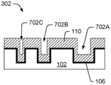
Referring to fig. 7A-7D, in various embodiments, equipment, techniques, and processes may be employed to mitigate the effects of undesirably high stresses (including the possibility of delamination due to expansion of the metal 110), improve yield, and reduce the cost of ownership of forming a flat metal in a large cavity 104. This may allow for the use of larger diameter structures 114, larger volume structures 114, or mixed size structures 114. Illustratively, the diameter of 114A is greater than the diameter of 114B, which in turn is greater than the diameter of 114C.
For example, in various embodiments, the opening 702 may be intentionally formed in the conductive interconnect structure 114. The opening 702 may extend a predetermined depth below the surface of the conductive interconnect 114. For a given metal coating time, the volume of the opening of 702A may be greater than the volume of the opening of 702B, and the volume of the opening 702B may be greater than the volume of 702C. The volume of the opening 702 may be selected based on the material 110 of the conductive interconnect 114, the thickness or volume of its material 110, and its expected expansion during annealing. In various embodiments, the opening 702 may include any recess, gap, cavity, void, etc. in the conductive interconnect structure 114 that provides expanded space for the material 110 of the interconnect structure 114. The appropriately sized openings 702 may reduce or eliminate stress of the expansion material 110 on the bond contacts 306 of the stacked die 302 or wafer, as the metal 110 may expand into the openings 702. The width of the opening 702 may range, for example, between less than 100nm and greater than 20 microns. With the opening 702 of a predetermined size, it may still allow the material 110 of the respective interconnect structure 114 to reliably bond and form a continuous conductive interconnect 310 between the stacked dies 302 or wafers.
In various embodiments, the openings 702 may be intentionally formed to have a desired preselected volume (e.g., to accommodate excessive stress due to thermal expansion mismatch of the coating metal 110 in the cavity 104 and the surrounding insulator 102 material). In other embodiments, the opening 702 may be allowed to be formed as part of the bonding surface 306 of the processing die 302 or wafer. In this case, the volume of the opening 702 may be predictable based on the process and materials involved.
For example, in some embodiments, the opening 702 may be intentionally formed when forming the conductive interconnect structure 114. For example, as shown at fig. 7A-7C, the conductive interconnect structure 114 may be formed using damascene techniques and may include a cavity 104 and a structure 114 having a mixed width (104A, 104B, and 104C) and depth. As shown at fig. 7A, one or more damascene cavities 104 may be formed in the surface of the dielectric layer 102 of the die 302 or wafer or substrate of interest to extend partially or fully through the dielectric layer 102. In one example, the cavity 104 may have a width or diameter of at least 10 microns, a depth of at least 5 microns or even 10 microns. Alternatively, the cavity 104 may be formed to extend into a base substrate (not shown, see, e.g., base 604 at fig. 6) of the die 302 or wafer. Barrier layer 106 and seed layer 108 are deposited over the exposed surfaces of cavity 104.
As shown at fig. 7B, the cavity 104 is partially filled with a conductive material 110 (e.g., copper alloy, etc.) using an superfill electroplating bath, or using a conformal electroplating or electroless plating bath, etc. In some embodiments, conductive layer 110 may be applied into chamber 104 by Physical Vapor Deposition (PVD) or by atomic layer deposition, chemical vapor deposition, or spin coating conductive layer 110 into chamber 104. The partial filling of the conductive layer 110 in the cavity 104 creates a conductive interconnect structure 114 having intentional openings 702 (e.g., 702A, 702B, and 702C) within the damascene cavity 104 (e.g., 104A, 104B, and 104C, respectively).
The bonding surface 306 of the die 302 or wafer or substrate of interest is planarized (using Chemical Mechanical Polishing (CMP) or the like) to prepare the dielectric surface 102 and conductive interconnect structure 114 for bonding. This includes removing unwanted plating 110 and other conductive barrier layers 106 from the damascene process from the dielectric bonding surface 306 as shown in fig. 7C. The remaining openings 702 '(e.g., 702A', 702B ', and 702C') are confined in the interconnect structure 114 and may have a predetermined volume. In one embodiment, the width ("w") of the remaining opening 702' at the bonding surface 306 of the die 302 or wafer is greater than the thickness of the barrier layer 106 between the conductive layer 110 and the dielectric layer 102. Thus, the width of the remaining opening 702A 'is greater than the width of the remaining opening 702B', and the width of the remaining opening 702B 'is greater than the width of the remaining opening 702C'. In other applications, the width ("w") of the remaining opening 702' at the bonding surface 306 is greater than the thickness of the conductive layer 110 within the corresponding cavity 104. In some applications, the depth ("d") of the remaining openings 702' may be less than 50nm, and preferably less than 100 microns.
The bonding surface 306 of the die 302 or wafer may be prepared for bonding with another similar die 302 or wafer, or with other prepared substrates 704, to form a bonding apparatus 312. In various embodiments, the substrate 704 may include the same or dissimilar or different material as the die 302. For example, the substrate 704 may include a dielectric, glass, semiconductor, or other material. After the bonding operation, in which one or more planar portions of the conductive interconnect structures 114(114A, 114B, and 114C) on the bonding surface 306 are bonded directly to the prepared surface of the opposing substrate 704, the remaining openings 702' are enclosed within the conductive interconnect structures 114, as shown in fig. 7D.
In an alternative process, as shown at fig. 8A-8D, after partially filling damascene cavity 104 with conductive material 110, a protective layer 802 (see fig. 8C and 8D) may be formed (e.g., deposited, coated, etc.) over the surface of conductive material 110, including within opening 702 of the surface of conductive interconnect structure 114.
In various embodiments, protective layer 802 may comprise a dielectric material, such as SiO2、SiC、SiN、SiC/SiO2、SiN/SiO2SiN/polysilicon, inorganic/organic dielectrics, etc. For example, the protective layer 802 may include the same or different dielectric as the die 302 or the insulating layer 102 of the wafer surface. In other embodiments, the protective layer 802 may comprise a conductive material such as tungsten, alloys of tungsten, nickel alloys, tantalum or titanium, and various alloys, such as TaN/Ta or Ta/TaN, Ti/TiN, cobalt, CoP, NiP, CoWP, CoP/NiP, and the like. Still further, the protective layer 802 may include a low CTEA material, a silicon-containing material such as doped or undoped polysilicon (which may form a silicide), or other suitable material. Still further, multiple coatings or layers of insulating and/or conductive materials may be used.
The protective layer may be deposited by PVD methods or by electrolytic or non-electrolytic plating baths or other techniques. Alternatively, protective layer 802 may include multiple coatings or layers of insulating and/or conductive materials. In some applications, protective layer 802 may include a conformal coating of one or more materials. One of the benefits of the protective layer 802 is to inhibit surface movement of metal atoms on the surface of the conductive layer 110 adjacent to the protective layer 802 within the opening 702, thereby improving the reliability of the bonded interconnect 114. Thus, the protective layer 802 may serve as a bonding surface for a portion of the conductive interconnect 114.
In one embodiment, the thickness of the protective layer 802 is less than the thickness of the conductive layer 110 within the respective cavity 104 bounded by the protective layer 802 and the barrier layer 106. In other embodiments, the protective layer 802 may be thicker than the conductive layer 110. After planarizing the bonding surface 306 (including removing unwanted material from the bonding surface 306), the remaining openings 702 ' (702A ', 702B ', and 702C ') in the surface of the interconnect structure 114 remain as the protective layer 802 on the inner surfaces of the remaining openings 702 ' (which may have a predetermined volume).
The die 302 or wafer may be prepared for bonding to another similar die 302 or wafer (as shown at fig. 3F, 3G, 9B, and 9C), and/or to some other prepared substrate 704 (as shown at fig. 7D, 9A, and 9C) to form the bonding apparatus 312. In one embodiment, the planarized wafer of FIG. 8D can be singulated by known methods, the singulated wafer cleaned and prepared for bonding operations. For example, a die 302 or wafer from a singulated wafer may be bonded to a flat substrate 704 or other carrier to form a bonding apparatus 312. In one embodiment, the planar carrier 704 or die 302 may include a single-level or multi-level BEOL interconnect structure 114 or a dielectric including one or more RDL layers. During the bonding operation, the conductive interconnect structures 114 of the die 302 align and mate with the receiving conductive interconnect structures 114 on the surface of a similar die 302 or wafer and/or prepared substrate 704 to form the unified conductive structure 310.
In various instances, as shown at fig. 9A-9C, the die 302 or wafer may be bonded front-to-front (fig. 9B) or back-to-front (fig. 9C) and/or bonded to a planar substrate 704 (fig. 9A and 9C) to form the bonding apparatus 312. After bonding, the conductive interconnect structure 114 has an enclosed cavity 702 ', with the protective layer 802 lining the inner surface of the cavity 702'. The profile of the one or more enclosed cavities 702' can be geometrically regular or irregular in shape as viewed in cross-section of the die 302. In various embodiments, the receiving substrate 704 may include a conductive layer that encloses one or more cavities 702', as shown at fig. 9A and 9C.
In other words, in an example embodiment, as shown at fig. 7D, the bonding apparatus 312 may include a portion of a conductive layer that is directly bonded to the substrate 704 (e.g., a portion of the conductive interconnect 114 at the bonding surface of the die 302) and may include another portion of the conductive layer that is not bonded to the same substrate 704 (e.g., an interior portion of the closed cavity 702' within the conductive interconnect 114). And in another embodiment, as shown at fig. 9A, the bonding apparatus 312 may include a portion of the conductive layer directly bonded to the substrate 704 (e.g., a portion of the conductive interconnect 114 at the bonding surface of the die 302) and may include another portion of the conductive layer directly coated with the protective layer 802 that is not bonded to the same substrate 704 (e.g., an interior portion of the closed cavity 702' within the conductive interconnect 114).
In some applications, where the wafer or die 302 includes TSVs or through-electrodes, after the bonding operation as shown in fig. 9B, the back side of the bonded wafer of die 302 may be thinned and formed to expose the back side of the conductive structures (TSVs or through-electrodes). Additional prepared dies 302 or wafers may be electrically coupled to the exposed TSVs on the back side of the bonded die 302 or wafer. The electrical coupling of the die 302 or wafer may include, among other things, using a DBI method or a flip chip method.
Further embodiments
Further embodiments are shown at fig. 10A to 12. In one embodiment, as shown at fig. 10A-10D, the partial fill of conductive material 110 discussed above is applied thinner and corresponds to a conformal or non-conformal metal coating 1002 within damascene cavity 104. Depending on the thickness of the conductive layer 1002, this thinner coating 1002 may result in an opening 702' that has a very large volume relative to the conductive interconnect structure 114.
In addition, as shown at fig. 10B, the coating 1002 may be thicker in some cases, or of varying thickness for different devices 312 or within a single device 312. For example, in some embodiments, the cross-sectional width ("w") of the opening 702' is greater than 3 times the thickness ("t") of the conductive layer 1002 (e.g., on the sidewalls of the cavity 104). Further, in some embodiments, the depth ("d") of the opening 702 'may be greater than the cross-sectional width ("w") of the opening 702'.
In one embodiment, as shown at fig. 10C, the inner surface of opening 702' (i.e., the exposed surface of conductive layer 1002) may be coated with protective coating 802 as described above. In another embodiment, as shown at fig. 10D, a compliant material 1004 (e.g., such as a fill material or an encapsulation material) may be deposited within the opening 702' of the conductive interconnect structure 114 (with or without the protective layer 802). The compliant material 1004 may partially or completely fill the opening 702.
Referring to fig. 11A-12, in some embodiments, the described techniques and processes may be used to form through silicon vias 1102 (TSVs), etc. for the device 312. In the case of TSV 1102, multiple layers may line the inner sidewalls of opening 702 within TSV 1102. In some embodiments, the TSVs 1102 may be formed by an intermediate via or last via approach. In the case of an intermediate via process, a backside exposure process may be applied to expose a portion of conductive interconnect structure 114 from the backside, regardless of how TSV 1102 or through-substrate via or through-glass via (TGV) or through-substrate electrode (TSE) or through-board via is formed.
For example, as shown at fig. 11A and 11B, after partially filling the cavity 104, one or more additional layers 1104 may be applied over the conductive layer 110, with or without the protective layer 802 (depending on the embodiment). In various examples, the one or more additional layers 1104 may include one or more dielectric layers or the like.
As shown at fig. 11B, planarizing the bonding surface 306 forms a conductive interconnect 114 with one or more additional layers 1104. Referring to fig. 11C, the backside of die 302 may be thinned and the backside of conductive interconnect 114 exposed by grinding, polishing, reactive ion etching methods, and other known methods to expose the interior of conductive interconnect structure 114, which forms TSV 1102. The TSV 1102 provides a hollow or through conductive opening 702 through the die 302, as shown at fig. 11C and 11D. In some embodiments, as shown, the inner conductive surface of the through opening 702 is lined with a dielectric layer 1104. The prepared backside may then be bonded directly to another die 302, a wafer, or a prepared substrate 704.
As shown at fig. 11D, one or more components 1106 (such as optical devices or other microelectronic components) may be bonded to the front bonding surface 306 of the die 302. In some cases, the TSVs 1102 provide electrical or optical signal transmission from one or more components 1106 to other dies 302, wafers, or prepared substrates 704 (bonded to the back side of the dies 302). For example, as shown at fig. 12, an optical device 312 is shown. In this example, the substrate 704 may include one or more layers of glass 1202 and include a reflector 1204 and optionally a cavity 1206 as required by the application. In this case, the TSVs 1102 may transmit optical signals, and in some cases, electrical signals as well.
In various other embodiments, other techniques may be used to modify the surface of the conductive interconnect structure 114 to mitigate the effects of metal expansion. For example, in some examples, the surface of the conductive interconnect structure 114 may be selectively etched (via acid etching, plasma oxidation, etc.) to provide a desired opening 702 depth. In further embodiments, the conductive interconnect structure 114 may be selected, formed, or processed to have a top surface that is not flat. For example, the top surface of the conductive interconnect structure may be rounded, domed, convex, concave, irregular, or otherwise non-planar.
Example procedure
Fig. 13 and 14 include text-based process flows for the above-described processes and techniques. Application of the described process flow provides for the use of conductive interconnect structures of greater width or diameter (e.g., 10-1000 microns, for example) at the bonding surface of a directly bonded die, wafer, substrate, or the like.
The order in which the processes are described is not intended to be construed as a limitation, and any number of the described process blocks in a process can be combined in any order to implement a process, or an alternative process. Moreover, individual blocks may be deleted from the processes without departing from the spirit and scope of the subject matter described herein. Further, the processes may be implemented in any suitable hardware, software, firmware, or combination thereof, without departing from the scope of the subject matter described herein. In alternative embodiments, other techniques may be included in the process in various combinations and still be within the scope of the present disclosure.
Fig. 13 illustrates a representative process 1300 of mitigating undesired recesses (e.g., such as recess 116) in a surface of a conductive interconnect structure (e.g., such as conductive interconnect structure 114) at a bonding surface of a die of interest (e.g., such as die 302), a wafer, or other substrate, in accordance with various embodiments. For example, an embedding layer (e.g., such as embedding layer 304) may be formed in the recess, filling the recess to provide a flat and smooth bonding surface suitable for direct bonding. Process 1300 refers to fig. 1A-6.
In one embodiment, at block 1302, process 1300 includes: one or more first embedded conductive interconnect structures (e.g., such as conductive interconnect structure 114) are formed in a first substrate (e.g., such as die 302).
At block 1304, the process includes planarizing a first surface of the first substrate to form a planar topography including the first surface and a surface of the one or more first embedded conductive interconnect structures. At block 1306, the process includes depositing a first embedding layer (e.g., such as embedding layer 304) over the first surface of the first substrate and the one or more first embedded conductive interconnect structures.
At block 1308, the process includes: planarizing the first embedding layer until a surface of the one or more first embedded conductive interconnect structures is exposed, and forming a bonding surface of the first embedding layer, the first recessed portions of the one or more first embedded conductive interconnect structures at least partially filling with a portion of the first embedding layer that covers the surface of the first recessed portions of the one or more first embedded conductive interconnect structures.
In one embodiment, a process comprises: by covering the surface of the first concave portion with the first embedding layer, surface movement of atoms of the material of the first concave portion is suppressed.
In one embodiment, a process comprises: forming one or more second embedded conductive interconnect structures in a second substrate; planarizing the first surface of the second substrate to form a planar topography comprising the first surface of the second substrate and surfaces of the one or more second embedded conductive interconnect structures; bonding the first surface of the second substrate to the bonding surface of the first substrate via direct bonding without an adhesive; and directly bonding the one or more second embedded conductive interconnect structures to the one or more first embedded conductive interconnect structures.
In another embodiment, a process comprises: depositing a second embedded layer over the first surface of the second substrate and the one or more second embedded conductive interconnect structures; and planarizing the second embedding layer until a surface of the one or more second embedded conductive interconnect structures is exposed and a second bonding surface of the second bonding layer is formed, the first recessed portions of the one or more second embedded conductive interconnect structures being at least partially filled with a portion of the second embedding layer that covers the surface of the first recessed portions of the one or more second embedded conductive interconnect structures.
In one embodiment, the process further comprises: a portion of the second embedding layer is bonded to a portion of the first embedding layer via direct bonding without an adhesive.
As an alternative embodiment, the process comprises: forming one or more first embedded conductive interconnect structures in a first substrate; planarizing a first surface of a first substrate to form a planarized topography comprising the first surface and a surface of one or more first embedded conductive interconnect structures; selectively removing a portion of the first surface to cause the one or more first embedded conductive interconnect structures to protrude above the first surface of the first substrate; depositing a first embedded layer over the first surface of the first substrate and the one or more first embedded conductive interconnect structures, the first embedded layer contacting a portion of the sidewalls of the one or more first embedded conductive interconnect structures; and planarizing the first embedding layer until a surface of the one or more first embedded conductive interconnect structures is exposed, and forming a bonding surface of the first embedding layer and a surface of the one or more first embedded conductive interconnect structures.
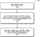
Fig. 14 illustrates a representative process 1400 of forming an opening (e.g., such as opening 702) in a surface of a conductive interconnect structure (e.g., such as conductive interconnect structure 114) at a bonding surface of a die of interest (e.g., such as die 302), a wafer, or other substrate, in accordance with various embodiments. For example, the opening may be formed in the conductive interconnect structure. Process 1400 refers to fig. 7A-12.
In one embodiment, at block 1402, the process 1400 includes forming one or more first cavities in a first surface of a first substrate.
At block 1404, the process includes forming one or more first embedded conductive interconnect structures within the one or more first cavities, including forming one or more of the first embedded conductive interconnect structures to have a first recessed portion in an exposed surface of the one or more first embedded conductive interconnect structures.
In one embodiment, a process comprises: one or more first embedded conductive interconnect structures and first recesses are formed by partially filling the one or more first cavities using a damascene process. In one embodiment, the one or more first embedded conductive interconnect structures include a conformal metal coating over one or more interior surfaces of the one or more first cavities.
In one embodiment, the process includes depositing a protective layer over the first recessed portion of the one or more first embedded conductive interconnect structures. In further embodiments, the process includes depositing one or more additional layers over the protective layer, at least one of the one or more additional layers including a dielectric material.
At block 1406, the process includes: the first surface of the first substrate is planarized to form a first planar bonding surface comprising the first surface and exposed surfaces of the one or more first embedded conductive interconnect structures.
In one embodiment, the process includes forming one or more second embedded conductive interconnect structures in a second substrate, including forming the one or more second embedded conductive interconnect structures in the second embedded conductive interconnect structures to have second recessed portions in exposed surfaces of the one or more second embedded conductive interconnect structures; planarizing the first surface of the second substrate to form a second planar bonding surface comprising the first surface of the second substrate and exposed surfaces of the one or more second embedded conductive interconnect structures; bonding the second planar bonding surface of the second substrate to the first planar bonding surface of the first substrate via direct bonding without an adhesive; and directly bonding the one or more second embedded conductive interconnect structures to the one or more first embedded conductive interconnect structures.
In further embodiments, the process includes depositing a protective layer over the second recessed portion of the one or more second embedded conductive interconnect structures. In an example, a process includes: by covering the surface of the second recessed portion with the protective layer, surface movement of atoms of the material of the second recessed portion is suppressed. In another example, the process includes: the direction of expansion of the material of the one or more second embedded conductive interconnect structures is controlled by covering the surface of the second recess with a protective layer.
As an alternative embodiment, the process comprises: forming one or more first cavities in a first surface of a first substrate; forming one or more first embedded conductive interconnect structures having one or more openings within one or more first cavities; and forming a planar surface comprising one or more of the first embedded conductive interconnect structures having one or more openings.
As another alternative embodiment, the process comprises: forming one or more first cavities in a first surface of a first substrate; forming one or more first embedded conductive interconnect structures having one or more openings within one or more first cavities; forming a planar surface comprising one or more first embedded conductive interconnect structures in a first embedded conductive interconnect structure having one or more openings; and directly bonding the planar surface of the interconnect structure having the opening to the prepared surface of the second substrate.
In various embodiments, some process steps may be modified or eliminated as compared to those described herein.
The techniques, components, and apparatus described herein are not limited to the illustrations of fig. 1A-15, and may be applied to other designs, types, arrangements, and configurations, including with other electrical components, without departing from the scope of the present disclosure. In some cases, the techniques described herein may be implemented using additional or alternative components, techniques, sequences, or processes. Further, the components and/or techniques may be arranged and/or combined in various combinations while producing similar or nearly identical results.
Conclusion
Although embodiments of the disclosure have been described in language specific to structural features and/or methodological acts, it is to be understood that the embodiments are not necessarily limited to the specific features or acts described. Rather, the specific features and acts are disclosed as representative forms of implementing example devices and techniques.

Claims (26)

1. A microelectronic assembly, comprising:
a first substrate having a bonding surface, the bonding surface of the first substrate having a flat topography;
a first conductive interconnect structure and a second conductive interconnect structure embedded in the first substrate and exposed at the bonding surface of the first substrate, the second conductive interconnect structure having a larger surface area at the bonding surface than the first conductive interconnect structure;
a first recess portion disposed in a surface of the first conductive interconnect structure; and
a second recess disposed in a surface of the second conductive interconnect structure, the second recess having a larger volume than the first recess, the first and second recesses being at least partially filled with a first embedding layer.
2. The microelectronic assembly of claim 1, further comprising: a second substrate having a bonding surface, the bonding surface of the second substrate having a planar topography and being bonded directly to the bonding surface of the first substrate without an adhesive; and
a first conductive interconnect structure and a second conductive interconnect structure embedded in the second substrate and exposed at the bonding surface of the second substrate, the second conductive interconnect structure of the second substrate having a larger surface area at the bonding surface than the first conductive interconnect structure of the second substrate, the first conductive interconnect structure of the second substrate being directly bonded to the first conductive interconnect structure of the first substrate, and the second conductive interconnect structure of the second substrate being directly bonded to the second conductive interconnect structure of the first substrate.
3. The microelectronic assembly of claim 2, further comprising: a first recess portion disposed in a surface of the first conductive interconnect structure of the second substrate; and a second recess disposed in a surface of the second conductive interconnect structure of the second substrate, the first and second recesses of the second substrate being at least partially filled with a second embedding layer, the second embedding layer being bonded directly to the first embedding layer without an adhesive.
4. The microelectronic assembly of claim 3, wherein the first conductive interconnect structures of the first and second substrates form a first conductive interconnect and the second conductive interconnect structures of the first and second substrates form a second conductive interconnect, and wherein the first recessed portions of the first and second substrates form a first cavity within the first conductive interconnect and the second recessed portions of the first and second substrates form a second cavity within the second conductive interconnect, the first and second cavities being completely lined with the second and first embedding layers.
5. The microelectronic assembly of claim 4, wherein a volume of the second cavity is greater than a volume of the first cavity.
6. The microelectronic assembly as claimed in claim 1, further comprising one or more cavities in the surface of the first and/or second conductive interconnect structures of the first substrate within a perimeter of the first and/or second conductive interconnect structures of the first substrate, the one or more cavities being filled with the first embedding layer.
7. The microelectronic assembly as claimed in claim 2, wherein the second conductive interconnect structures of the first and second substrates have a surface width dimension greater than 5 microns.
8. The microelectronic assembly of claim 1, wherein the first embedded layer comprises a silicon-containing material.
9. The microelectronic assembly of claim 8, wherein the silicon-containing material comprises SiC, SiC/SiCh, SiN/SiCh, or a silicide.
10. The microelectronic assembly of claim 1, wherein the conductive material of the first embedding layer is different from the material of the first and second conductive interconnect structures.
11. The microelectronic assembly of claim 1, wherein a melting point or Coefficient of Thermal Expansion (CTE) of a material of the first embedding layer is greater than a melting point or CTE of a material of the first conductive interconnect structure.
12. A microelectronic assembly, comprising:
a first substrate having a bonding surface, the bonding surface of the first substrate having a planar topography, a first conductive interconnect structure embedded in the first substrate, a first embedding layer on a portion of the surface of the first conductive interconnect structure;
a second substrate having a bonding surface, the bonding surface of the second substrate having a planar topography, a second conductive interconnect structure embedded in the second substrate, a second embedding layer on a portion of the surface of the second conductive interconnect structure;
a bonding interface at which the bonding surface of the first substrate is bonded to the bonding surface of the second substrate, the first and second embedded layers of the first and second substrates contacting and forming an enclosed cavity.
13. The microelectronic assembly of claim 12, wherein the first and second embedding layers conform to the first and second conductive interconnect structures, respectively.
14. The microelectronic assembly of claim 12, wherein the cavity extends more than 100nm below the bonding interface.
15. A microelectronic assembly, comprising:
a first substrate having a bonding surface, the bonding surface of the first substrate having a flat topography;
one or more first conductive interconnect structures embedded in the first substrate and exposed at the bonding surface of the first substrate; and
a first recess disposed in a surface of at least one of the one or more first conductive interconnect structures, wherein a depth of the first recess is greater than 20 nm.
16. The microelectronic assembly of claim 15, further comprising: a second substrate having a bonding surface, the bonding surface of the second substrate having a planar topography and being bonded directly to the bonding surface of the first substrate without an adhesive; and
one or more second conductive interconnect structures embedded in the second substrate and exposed at the bonding surface of the second substrate, the one or more second conductive interconnect structures being directly bonded to the one or more first conductive interconnect structures.
17. The microelectronic assembly of claim 16, further comprising a second recess disposed in a surface of at least one of the one or more second conductive interconnect structures, a volume of the second recess corresponding to an expansion of a material of the one or more second conductive interconnect structures when heated to a predetermined temperature.
18. The microelectronic assembly of claim 17, wherein the one or more second conductive interconnect structures and the one or more first conductive interconnect structures form one or more conductive interconnects, and wherein the first and second recessed portions form a cavity within at least one of the one or more conductive interconnects.
19. The microelectronic assembly of claim 18, wherein the cavity is partially or fully lined with a protective layer.
20. The microelectronic assembly of claim 19, wherein the protective layer comprises silicon.
21. The microelectronic assembly of claim 20, wherein the protective layer comprises SiC, SiC/SiOi, or SiN/SiO2
22. The microelectronic assembly of claim 19, wherein the protective layer comprises tungsten, an alloy of tungsten, nickel, an alloy of nickel, cobalt, an alloy of cobalt, tantalum, an alloy of tantalum, titanium, or an alloy of titanium.
23. The microelectronic assembly of claim 19, further comprising a dielectric layer disposed over the protective layer.
24. The microelectronic assembly of claim 15, wherein the first recessed portion is disposed within a perimeter of the one or more first conductive interconnect structures.
25. The microelectronic assembly of claim 15, wherein the one or more first conductive interconnect structures comprise a plurality of conductive interconnect structures having different widths and/or surface areas at the bonding surface.
26. The microelectronic assembly of claim 21, wherein the one or more first conductive interconnect structures have a surface width dimension greater than 10 microns.
CN201980077502.5A 2018-10-22 2019-10-21 Interconnect structure Active CN113169151B (en)

Applications Claiming Priority (7)

Application Number Priority Date Filing Date Title
US201862748653P 2018-10-22 2018-10-22
US62/748,653 2018-10-22
US201962902207P 2019-09-18 2019-09-18
US62/902,207 2019-09-18
US16/657,696 US11158573B2 (en) 2018-10-22 2019-10-18 Interconnect structures
US16/657,696 2019-10-18
PCT/US2019/057252 WO2020086477A1 (en) 2018-10-22 2019-10-21 Interconnect structures

Publications (2)

Publication Number Publication Date
CN113169151A true CN113169151A (en) 2021-07-23
CN113169151B CN113169151B (en) 2022-05-03

Family

ID=70279934

Family Applications (1)

Application Number Title Priority Date Filing Date
CN201980077502.5A Active CN113169151B (en) 2018-10-22 2019-10-21 Interconnect structure

Country Status (4)

Country Link
US (4) US11158573B2 (en)
KR (1) KR20210064388A (en)
CN (1) CN113169151B (en)
WO (1) WO2020086477A1 (en)

Cited By (3)

* Cited by examiner, † Cited by third party
Publication number Priority date Publication date Assignee Title
WO2023015492A1 (en) * 2021-08-11 2023-02-16 华为技术有限公司 Chip packaging structure and preparation method for chip packaging structure
CN115910817A (en) * 2022-12-05 2023-04-04 青岛物元技术有限公司 Wafer bonding method and semiconductor device
CN116613157A (en) * 2023-07-21 2023-08-18 荣耀终端有限公司 Chip stacking structure, manufacturing method thereof and electronic equipment

Families Citing this family (109)

* Cited by examiner, † Cited by third party
Publication number Priority date Publication date Assignee Title
US7109092B2 (en) 2003-05-19 2006-09-19 Ziptronix, Inc. Method of room temperature covalent bonding
US7485968B2 (en) 2005-08-11 2009-02-03 Ziptronix, Inc. 3D IC method and device
US8735219B2 (en) 2012-08-30 2014-05-27 Ziptronix, Inc. Heterogeneous annealing method and device
US20150262902A1 (en) 2014-03-12 2015-09-17 Invensas Corporation Integrated circuits protected by substrates with cavities, and methods of manufacture
US11069734B2 (en) 2014-12-11 2021-07-20 Invensas Corporation Image sensor device
US9741620B2 (en) 2015-06-24 2017-08-22 Invensas Corporation Structures and methods for reliable packages
US10886250B2 (en) 2015-07-10 2021-01-05 Invensas Corporation Structures and methods for low temperature bonding using nanoparticles
US9953941B2 (en) 2015-08-25 2018-04-24 Invensas Bonding Technologies, Inc. Conductive barrier direct hybrid bonding
US10204893B2 (en) 2016-05-19 2019-02-12 Invensas Bonding Technologies, Inc. Stacked dies and methods for forming bonded structures
US10672663B2 (en) 2016-10-07 2020-06-02 Xcelsis Corporation 3D chip sharing power circuit
US11176450B2 (en) 2017-08-03 2021-11-16 Xcelsis Corporation Three dimensional circuit implementing machine trained network
US10580735B2 (en) 2016-10-07 2020-03-03 Xcelsis Corporation Stacked IC structure with system level wiring on multiple sides of the IC die
TWI822659B (en) 2016-10-27 2023-11-21 美商艾德亞半導體科技有限責任公司 Structures and methods for low temperature bonding
US10002844B1 (en) 2016-12-21 2018-06-19 Invensas Bonding Technologies, Inc. Bonded structures
CN117878055A (en) 2016-12-28 2024-04-12 艾德亚半导体接合科技有限公司 Stacking substrate processing
US20180182665A1 (en) 2016-12-28 2018-06-28 Invensas Bonding Technologies, Inc. Processed Substrate
TW202431592A (en) 2016-12-29 2024-08-01 美商艾德亞半導體接合科技有限公司 Bonded structures with integrated passive component
WO2018169968A1 (en) 2017-03-16 2018-09-20 Invensas Corporation Direct-bonded led arrays and applications
US10515913B2 (en) 2017-03-17 2019-12-24 Invensas Bonding Technologies, Inc. Multi-metal contact structure
US10508030B2 (en) 2017-03-21 2019-12-17 Invensas Bonding Technologies, Inc. Seal for microelectronic assembly
US10269756B2 (en) 2017-04-21 2019-04-23 Invensas Bonding Technologies, Inc. Die processing
US10879212B2 (en) 2017-05-11 2020-12-29 Invensas Bonding Technologies, Inc. Processed stacked dies
US10446441B2 (en) 2017-06-05 2019-10-15 Invensas Corporation Flat metal features for microelectronics applications
US10217720B2 (en) 2017-06-15 2019-02-26 Invensas Corporation Multi-chip modules formed using wafer-level processing of a reconstitute wafer
CN109285825B (en) * 2017-07-21 2021-02-05 联华电子股份有限公司 Chip stacking structure and manufacturing method of tube core stacking structure
US10840205B2 (en) 2017-09-24 2020-11-17 Invensas Bonding Technologies, Inc. Chemical mechanical polishing for hybrid bonding
US11195748B2 (en) 2017-09-27 2021-12-07 Invensas Corporation Interconnect structures and methods for forming same
US11031285B2 (en) 2017-10-06 2021-06-08 Invensas Bonding Technologies, Inc. Diffusion barrier collar for interconnects
US11380597B2 (en) 2017-12-22 2022-07-05 Invensas Bonding Technologies, Inc. Bonded structures
US10923408B2 (en) 2017-12-22 2021-02-16 Invensas Bonding Technologies, Inc. Cavity packages
US10727219B2 (en) 2018-02-15 2020-07-28 Invensas Bonding Technologies, Inc. Techniques for processing devices
US11169326B2 (en) 2018-02-26 2021-11-09 Invensas Bonding Technologies, Inc. Integrated optical waveguides, direct-bonded waveguide interface joints, optical routing and interconnects
US11256004B2 (en) 2018-03-20 2022-02-22 Invensas Bonding Technologies, Inc. Direct-bonded lamination for improved image clarity in optical devices
US10991804B2 (en) 2018-03-29 2021-04-27 Xcelsis Corporation Transistor level interconnection methodologies utilizing 3D interconnects
US11056348B2 (en) 2018-04-05 2021-07-06 Invensas Bonding Technologies, Inc. Bonding surfaces for microelectronics
US10790262B2 (en) 2018-04-11 2020-09-29 Invensas Bonding Technologies, Inc. Low temperature bonded structures
US11244916B2 (en) 2018-04-11 2022-02-08 Invensas Bonding Technologies, Inc. Low temperature bonded structures
US10964664B2 (en) 2018-04-20 2021-03-30 Invensas Bonding Technologies, Inc. DBI to Si bonding for simplified handle wafer
US11004757B2 (en) 2018-05-14 2021-05-11 Invensas Bonding Technologies, Inc. Bonded structures
US11276676B2 (en) 2018-05-15 2022-03-15 Invensas Bonding Technologies, Inc. Stacked devices and methods of fabrication
US10923413B2 (en) 2018-05-30 2021-02-16 Xcelsis Corporation Hard IP blocks with physically bidirectional passageways
CN112585740B (en) 2018-06-13 2025-05-13 隔热半导体粘合技术公司 TSV as a pad
US11393779B2 (en) 2018-06-13 2022-07-19 Invensas Bonding Technologies, Inc. Large metal pads over TSV
US10910344B2 (en) 2018-06-22 2021-02-02 Xcelsis Corporation Systems and methods for releveled bump planes for chiplets
WO2020010056A1 (en) 2018-07-03 2020-01-09 Invensas Bonding Technologies, Inc. Techniques for joining dissimilar materials in microelectronics
US11462419B2 (en) 2018-07-06 2022-10-04 Invensas Bonding Technologies, Inc. Microelectronic assemblies
US11158606B2 (en) 2018-07-06 2021-10-26 Invensas Bonding Technologies, Inc. Molded direct bonded and interconnected stack
US12406959B2 (en) 2018-07-26 2025-09-02 Adeia Semiconductor Bonding Technologies Inc. Post CMP processing for hybrid bonding
US11515291B2 (en) 2018-08-28 2022-11-29 Adeia Semiconductor Inc. Integrated voltage regulator and passive components
US11296044B2 (en) 2018-08-29 2022-04-05 Invensas Bonding Technologies, Inc. Bond enhancement structure in microelectronics for trapping contaminants during direct-bonding processes
US11011494B2 (en) 2018-08-31 2021-05-18 Invensas Bonding Technologies, Inc. Layer structures for making direct metal-to-metal bonds at low temperatures in microelectronics
US11158573B2 (en) 2018-10-22 2021-10-26 Invensas Bonding Technologies, Inc. Interconnect structures
US11244920B2 (en) 2018-12-18 2022-02-08 Invensas Bonding Technologies, Inc. Method and structures for low temperature device bonding
US11476213B2 (en) 2019-01-14 2022-10-18 Invensas Bonding Technologies, Inc. Bonded structures without intervening adhesive
US11387202B2 (en) 2019-03-01 2022-07-12 Invensas Llc Nanowire bonding interconnect for fine-pitch microelectronics
US11901281B2 (en) 2019-03-11 2024-02-13 Adeia Semiconductor Bonding Technologies Inc. Bonded structures with integrated passive component
US10854578B2 (en) 2019-03-29 2020-12-01 Invensas Corporation Diffused bitline replacement in stacked wafer memory
US11373963B2 (en) 2019-04-12 2022-06-28 Invensas Bonding Technologies, Inc. Protective elements for bonded structures
US11610846B2 (en) 2019-04-12 2023-03-21 Adeia Semiconductor Bonding Technologies Inc. Protective elements for bonded structures including an obstructive element
US11205625B2 (en) 2019-04-12 2021-12-21 Invensas Bonding Technologies, Inc. Wafer-level bonding of obstructive elements
US11355404B2 (en) 2019-04-22 2022-06-07 Invensas Bonding Technologies, Inc. Mitigating surface damage of probe pads in preparation for direct bonding of a substrate
US11385278B2 (en) 2019-05-23 2022-07-12 Invensas Bonding Technologies, Inc. Security circuitry for bonded structures
US12374641B2 (en) 2019-06-12 2025-07-29 Adeia Semiconductor Bonding Technologies Inc. Sealed bonded structures and methods for forming the same
US11296053B2 (en) 2019-06-26 2022-04-05 Invensas Bonding Technologies, Inc. Direct bonded stack structures for increased reliability and improved yield in microelectronics
US12080672B2 (en) 2019-09-26 2024-09-03 Adeia Semiconductor Bonding Technologies Inc. Direct gang bonding methods including directly bonding first element to second element to form bonded structure without adhesive
US12113054B2 (en) 2019-10-21 2024-10-08 Adeia Semiconductor Technologies Llc Non-volatile dynamic random access memory
US11862602B2 (en) 2019-11-07 2024-01-02 Adeia Semiconductor Technologies Llc Scalable architecture for reduced cycles across SOC
US11762200B2 (en) 2019-12-17 2023-09-19 Adeia Semiconductor Bonding Technologies Inc. Bonded optical devices
US11876076B2 (en) 2019-12-20 2024-01-16 Adeia Semiconductor Technologies Llc Apparatus for non-volatile random access memory stacks
US11721653B2 (en) 2019-12-23 2023-08-08 Adeia Semiconductor Bonding Technologies Inc. Circuitry for electrical redundancy in bonded structures
US11842894B2 (en) 2019-12-23 2023-12-12 Adeia Semiconductor Bonding Technologies Inc. Electrical redundancy for bonded structures
WO2021188846A1 (en) 2020-03-19 2021-09-23 Invensas Bonding Technologies, Inc. Dimension compensation control for directly bonded structures
US11742314B2 (en) 2020-03-31 2023-08-29 Adeia Semiconductor Bonding Technologies Inc. Reliable hybrid bonded apparatus
US11735523B2 (en) * 2020-05-19 2023-08-22 Adeia Semiconductor Bonding Technologies Inc. Laterally unconfined structure
US11631647B2 (en) 2020-06-30 2023-04-18 Adeia Semiconductor Bonding Technologies Inc. Integrated device packages with integrated device die and dummy element
US11430753B2 (en) * 2020-07-08 2022-08-30 Raytheon Company Iterative formation of damascene interconnects
KR102803130B1 (en) 2020-08-14 2025-05-07 삼성전자주식회사 Semiconductor package and method of manufacturing the semiconductor package
US11764177B2 (en) 2020-09-04 2023-09-19 Adeia Semiconductor Bonding Technologies Inc. Bonded structure with interconnect structure
US11728273B2 (en) 2020-09-04 2023-08-15 Adeia Semiconductor Bonding Technologies Inc. Bonded structure with interconnect structure
US11990448B2 (en) 2020-09-18 2024-05-21 Intel Corporation Direct bonding in microelectronic assemblies
US12199018B2 (en) * 2020-09-18 2025-01-14 Intel Corporation Direct bonding in microelectronic assemblies
US11264357B1 (en) 2020-10-20 2022-03-01 Invensas Corporation Mixed exposure for large die
KR20230097121A (en) 2020-10-29 2023-06-30 아데이아 세미컨덕터 본딩 테크놀로지스 인코포레이티드 Direct bonding method and structure
US11527501B1 (en) * 2020-12-15 2022-12-13 Intel Corporation Sacrificial redistribution layer in microelectronic assemblies having direct bonding
KR20230125309A (en) 2020-12-28 2023-08-29 아데이아 세미컨덕터 본딩 테크놀로지스 인코포레이티드 Structures having through-substrate vias and methods for forming the same
EP4268274A4 (en) 2020-12-28 2024-10-30 Adeia Semiconductor Bonding Technologies Inc. STRUCTURES WITH SUBSTRATE PASSAGES AND METHODS FOR FORMING THE SAME
KR20230126736A (en) 2020-12-30 2023-08-30 아데이아 세미컨덕터 본딩 테크놀로지스 인코포레이티드 Structures with Conductive Features and Methods of Forming The Same
US11562974B2 (en) * 2021-01-07 2023-01-24 United Microelectronics Corp. Hybrid bonding structure and method of fabricating the same
EP4315398A4 (en) 2021-03-31 2025-03-05 Adeia Semiconductor Bonding Technologies Inc. Direct bonding and debonding of carrier
CN115274595B (en) * 2021-04-30 2024-12-06 长鑫存储技术有限公司 Semiconductor structure and its manufacturing method and wafer bonding method
EP4181187B1 (en) * 2021-07-01 2025-05-21 Changxin Memory Technologies, Inc. Semiconductor structure and manufacturing method thereof
KR20240036698A (en) 2021-08-02 2024-03-20 아데이아 세미컨덕터 본딩 테크놀로지스 인코포레이티드 Protective semiconductor elements for combined structures
JP2023034974A (en) * 2021-08-31 2023-03-13 キオクシア株式会社 Semiconductor device and substrate
EP4406020A4 (en) 2021-09-24 2026-01-21 Adeia Semiconductor Bonding Technologies Inc STRUCTURE LINKED WITH ACTIVE INTERPOSER
WO2023122509A1 (en) 2021-12-20 2023-06-29 Adeia Semiconductor Bonding Technologies Inc. Thermoelectric cooling for die packages
US20230197618A1 (en) * 2021-12-21 2023-06-22 Intel Corporation Multilayer glass substrate
US20230197655A1 (en) * 2021-12-22 2023-06-22 Adeia Semiconductor Bonding Technologies Inc. Low stress direct hybrid bonding
EP4515594A1 (en) 2022-04-25 2025-03-05 Adeia Semiconductor Bonding Technologies Inc. Expansion controlled structure for direct bonding and method of forming same
CN117747573A (en) * 2022-09-13 2024-03-22 华为技术有限公司 Chip packaging structure, manufacturing method thereof and electronic equipment
US12444672B2 (en) * 2022-09-30 2025-10-14 Intel Corporation Hybrid bonding technologies with thermal expansion compensation structures
KR20240094883A (en) * 2022-12-16 2024-06-25 삼성전자주식회사 Wafer-to-wafer bonding structure and image sensor using the same
US12506114B2 (en) 2022-12-29 2025-12-23 Adeia Semiconductor Bonding Technologies Inc. Directly bonded metal structures having aluminum features and methods of preparing same
US12341083B2 (en) 2023-02-08 2025-06-24 Adeia Semiconductor Bonding Technologies Inc. Electronic device cooling structures bonded to semiconductor elements
KR20240139871A (en) * 2023-03-15 2024-09-24 삼성전자주식회사 Bonding semiconductor device, and chip for bonding semiconductor device and method of manufacturing the same
US20250006677A1 (en) * 2023-06-27 2025-01-02 Taiwan Semiconductor Manufacturing Co., Ltd. Bond Features For Reducing Non-Bond and Methods of Forming the Same
US20250079364A1 (en) * 2023-09-06 2025-03-06 Adeia Semiconductor Bonding Technologies Inc. Methods and structures employing metal oxide for direct metal bonding
WO2025178884A1 (en) * 2024-02-23 2025-08-28 Tokyo Electron Limited Method for die-to-die hybrid bonding using an advanced distribution model
US20250372554A1 (en) * 2024-05-29 2025-12-04 Adeia Semiconductor Bonding Technologies Inc. Pad-less hybrid bonding
US20250391794A1 (en) * 2024-06-21 2025-12-25 Adeia Semiconductor Bonding Technologies Inc. Composite hybrid structures

Citations (7)

* Cited by examiner, † Cited by third party
Publication number Priority date Publication date Assignee Title
TW442909B (en) * 1999-07-07 2001-06-23 Taiwan Semiconductor Mfg Manufacturing method of copper dual damascene interconnect
CN1926680A (en) * 2004-02-26 2007-03-07 国际商业机器公司 Integrated circuit chip utilizing carbon nanotube composite interconnection vias
US20070296073A1 (en) * 2006-06-27 2007-12-27 Taiwan Semiconductor Manufacturing Co., Ltd. Three dimensional integrated circuit and method of making the same
CN101154616A (en) * 2006-09-30 2008-04-02 中芯国际集成电路制造(上海)有限公司 Method for forming shallow trench isolation structure
US20130020704A1 (en) * 2011-07-18 2013-01-24 S.O.I.Tec Silicon On Insulator Technologies Bonding surfaces for direct bonding of semiconductor structures
US20130320556A1 (en) * 2012-06-05 2013-12-05 Taiwan Semiconductor Manufacturing Company, Ltd. Three Dimensional Integrated Circuit Structures and Hybrid Bonding Methods for Semiconductor Wafers
US20140117546A1 (en) * 2012-06-05 2014-05-01 Taiwan Semiconductor Manufacturing Company, Ltd. Hybrid bonding mechanisms for semiconductor wafers

Family Cites Families (410)

* Cited by examiner, † Cited by third party
Publication number Priority date Publication date Assignee Title
JPS6130059A (en) 1984-07-20 1986-02-12 Nec Corp Manufacture of semiconductor device
KR900008647B1 (en) 1986-03-20 1990-11-26 후지쓰 가부시끼가이샤 A method for manufacturing three demensional i.c.
JPH07112041B2 (en) 1986-12-03 1995-11-29 シャープ株式会社 Method for manufacturing semiconductor device
US4904328A (en) 1987-09-08 1990-02-27 Gencorp Inc. Bonding of FRP parts
US4784970A (en) 1987-11-18 1988-11-15 Grumman Aerospace Corporation Process for making a double wafer moated signal processor
JPH0272642A (en) 1988-09-07 1990-03-12 Nec Corp Structure and method for connecting substrates
JPH0344067A (en) 1989-07-11 1991-02-25 Nec Corp Laminating method of semiconductor substrate
US5489804A (en) 1989-08-28 1996-02-06 Lsi Logic Corporation Flexible preformed planar structures for interposing between a chip and a substrate
JP3190057B2 (en) 1990-07-02 2001-07-16 株式会社東芝 Composite integrated circuit device
JP2729413B2 (en) 1991-02-14 1998-03-18 三菱電機株式会社 Semiconductor device
JP2910334B2 (en) 1991-07-22 1999-06-23 富士電機株式会社 Joining method
JPH05198739A (en) 1991-09-10 1993-08-06 Mitsubishi Electric Corp Stacked semiconductor device and manufacturing method thereof
CA2083072C (en) 1991-11-21 1998-02-03 Shinichi Hasegawa Method for manufacturing polyimide multilayer wiring substrate
US6008126A (en) 1992-04-08 1999-12-28 Elm Technology Corporation Membrane dielectric isolation IC fabrication
US5236118A (en) 1992-05-12 1993-08-17 The Regents Of The University Of California Aligned wafer bonding
JPH0682753B2 (en) 1992-09-28 1994-10-19 株式会社東芝 Method for manufacturing semiconductor device
US5503704A (en) 1993-01-06 1996-04-02 The Regents Of The University Of California Nitrogen based low temperature direct bonding
DE59406156D1 (en) 1993-02-11 1998-07-16 Siemens Ag Method for producing a three-dimensional circuit arrangement
US5516727A (en) 1993-04-19 1996-05-14 International Business Machines Corporation Method for encapsulating light emitting diodes
JPH0766093A (en) 1993-08-23 1995-03-10 Sumitomo Sitix Corp Method and device for bonding semiconductor wafers
JP2560625B2 (en) 1993-10-29 1996-12-04 日本電気株式会社 Semiconductor device and manufacturing method thereof
EP0651449B1 (en) 1993-11-01 2002-02-13 Matsushita Electric Industrial Co., Ltd. Electronic component and method for producing the same
US5501003A (en) 1993-12-15 1996-03-26 Bel Fuse Inc. Method of assembling electronic packages for surface mount applications
US5442235A (en) 1993-12-23 1995-08-15 Motorola Inc. Semiconductor device having an improved metal interconnect structure
US5413952A (en) 1994-02-02 1995-05-09 Motorola, Inc. Direct wafer bonded structure method of making
JP3294934B2 (en) 1994-03-11 2002-06-24 キヤノン株式会社 Method for manufacturing semiconductor substrate and semiconductor substrate
JPH07283382A (en) 1994-04-12 1995-10-27 Sony Corp Silicon substrate bonding method
KR960009074A (en) 1994-08-29 1996-03-22 모리시다 요이치 Semiconductor device and manufacturing method thereof
JPH08125121A (en) 1994-08-29 1996-05-17 Matsushita Electric Ind Co Ltd Semiconductor device and manufacturing method thereof
JP3171366B2 (en) 1994-09-05 2001-05-28 三菱マテリアル株式会社 Silicon semiconductor wafer and method for manufacturing the same
DE4433330C2 (en) 1994-09-19 1997-01-30 Fraunhofer Ges Forschung Method for producing semiconductor structures with advantageous high-frequency properties and a semiconductor wafer structure
DE4433845A1 (en) 1994-09-22 1996-03-28 Fraunhofer Ges Forschung Method of manufacturing a three-dimensional integrated circuit
JPH08186235A (en) 1994-12-16 1996-07-16 Texas Instr Inc <Ti> Manufacture of semiconductor device
JP2679681B2 (en) 1995-04-28 1997-11-19 日本電気株式会社 Semiconductor device, package for semiconductor device, and manufacturing method thereof
US5610431A (en) 1995-05-12 1997-03-11 The Charles Stark Draper Laboratory, Inc. Covers for micromechanical sensors and other semiconductor devices
US5872051A (en) 1995-08-02 1999-02-16 International Business Machines Corporation Process for transferring material to semiconductor chip conductive pads using a transfer substrate
JP3490198B2 (en) 1995-10-25 2004-01-26 松下電器産業株式会社 Semiconductor device and manufacturing method thereof
JP3979687B2 (en) 1995-10-26 2007-09-19 アプライド マテリアルズ インコーポレイテッド Method for improving film stability of halogen-doped silicon oxide films
KR100438256B1 (en) 1995-12-18 2004-08-25 마츠시타 덴끼 산교 가부시키가이샤 Semiconductor device and manufacturing method
ATE204251T1 (en) 1996-05-14 2001-09-15 Degussa METHOD FOR PRODUCING TRIMETHYLHYDROQUINONE
US5956605A (en) 1996-09-20 1999-09-21 Micron Technology, Inc. Use of nitrides for flip-chip encapsulation
JP3383811B2 (en) 1996-10-28 2003-03-10 松下電器産業株式会社 Semiconductor chip module and method of manufacturing the same
US5888631A (en) 1996-11-08 1999-03-30 W. L. Gore & Associates, Inc. Method for minimizing warp in the production of electronic assemblies
US6054363A (en) 1996-11-15 2000-04-25 Canon Kabushiki Kaisha Method of manufacturing semiconductor article
US5821692A (en) 1996-11-26 1998-10-13 Motorola, Inc. Organic electroluminescent device hermetic encapsulation package
US6333206B1 (en) 1996-12-24 2001-12-25 Nitto Denko Corporation Process for the production of semiconductor device
US6221753B1 (en) 1997-01-24 2001-04-24 Micron Technology, Inc. Flip chip technique for chip assembly
JPH10223636A (en) 1997-02-12 1998-08-21 Nec Yamagata Ltd Manufacture of semiconductor integrated circuit device
JP4026882B2 (en) 1997-02-24 2007-12-26 三洋電機株式会社 Semiconductor device
US5929512A (en) 1997-03-18 1999-07-27 Jacobs; Richard L. Urethane encapsulated integrated circuits and compositions therefor
US5915167A (en) 1997-04-04 1999-06-22 Elm Technology Corporation Three dimensional structure memory
AU7147798A (en) 1997-04-23 1998-11-13 Advanced Chemical Systems International, Inc. Planarization compositions for cmp of interlayer dielectrics
JP4032454B2 (en) 1997-06-27 2008-01-16 ソニー株式会社 Manufacturing method of three-dimensional circuit element
US6097096A (en) 1997-07-11 2000-08-01 Advanced Micro Devices Metal attachment method and structure for attaching substrates at low temperatures
JPH11186120A (en) 1997-12-24 1999-07-09 Canon Inc Adhesion bonding between substrates of the same or different materials
US6137063A (en) 1998-02-27 2000-10-24 Micron Technology, Inc. Electrical interconnections
EP0951068A1 (en) 1998-04-17 1999-10-20 Interuniversitair Micro-Elektronica Centrum Vzw Method of fabrication of a microstructure having an inside cavity
US6147000A (en) 1998-08-11 2000-11-14 Advanced Micro Devices, Inc. Method for forming low dielectric passivation of copper interconnects
US6316786B1 (en) 1998-08-29 2001-11-13 International Business Machines Corporation Organic opto-electronic devices
JP2000100679A (en) 1998-09-22 2000-04-07 Canon Inc Micro-region solid-state bonding method between substrates by thinning and device structure
SG99289A1 (en) 1998-10-23 2003-10-27 Ibm Chemical-mechanical planarization of metallurgy
US6515343B1 (en) 1998-11-19 2003-02-04 Quicklogic Corporation Metal-to-metal antifuse with non-conductive diffusion barrier
US6409904B1 (en) 1998-12-01 2002-06-25 Nutool, Inc. Method and apparatus for depositing and controlling the texture of a thin film
US6123825A (en) 1998-12-02 2000-09-26 International Business Machines Corporation Electromigration-resistant copper microstructure and process of making
US6232150B1 (en) 1998-12-03 2001-05-15 The Regents Of The University Of Michigan Process for making microstructures and microstructures made thereby
JP3918350B2 (en) 1999-03-05 2007-05-23 セイコーエプソン株式会社 Manufacturing method of semiconductor device
US6348709B1 (en) 1999-03-15 2002-02-19 Micron Technology, Inc. Electrical contact for high dielectric constant capacitors and method for fabricating the same
JP3532788B2 (en) 1999-04-13 2004-05-31 唯知 須賀 Semiconductor device and manufacturing method thereof
US6259160B1 (en) 1999-04-21 2001-07-10 Advanced Micro Devices, Inc. Apparatus and method of encapsulated copper (Cu) Interconnect formation
JP2000311982A (en) 1999-04-26 2000-11-07 Toshiba Corp Semiconductor device, semiconductor module, and manufacturing method thereof
US6258625B1 (en) 1999-05-18 2001-07-10 International Business Machines Corporation Method of interconnecting electronic components using a plurality of conductive studs
KR100333384B1 (en) 1999-06-28 2002-04-18 박종섭 chip size stack package and method of fabricating the same
US6218203B1 (en) 1999-06-28 2001-04-17 Advantest Corp. Method of producing a contact structure
JP3619395B2 (en) 1999-07-30 2005-02-09 京セラ株式会社 Semiconductor device built-in wiring board and manufacturing method thereof
US6756253B1 (en) 1999-08-27 2004-06-29 Micron Technology, Inc. Method for fabricating a semiconductor component with external contact polymer support layer
US6583515B1 (en) 1999-09-03 2003-06-24 Texas Instruments Incorporated Ball grid array package for enhanced stress tolerance
US6593645B2 (en) 1999-09-24 2003-07-15 United Microelectronics Corp. Three-dimensional system-on-chip structure
JP2001102479A (en) 1999-09-27 2001-04-13 Toshiba Corp Semiconductor integrated circuit device and method of manufacturing the same
US6984571B1 (en) 1999-10-01 2006-01-10 Ziptronix, Inc. Three dimensional device integration method and integrated device
US6500694B1 (en) 2000-03-22 2002-12-31 Ziptronix, Inc. Three dimensional device integration method and integrated device
US6333120B1 (en) 1999-10-27 2001-12-25 International Business Machines Corporation Method for controlling the texture and microstructure of plated copper and plated structure
US6902987B1 (en) 2000-02-16 2005-06-07 Ziptronix, Inc. Method for low temperature bonding and bonded structure
WO2001084617A1 (en) 2000-04-27 2001-11-08 Nu Tool Inc. Conductive structure for use in multi-level metallization and process
JP4123682B2 (en) 2000-05-16 2008-07-23 セイコーエプソン株式会社 Semiconductor device and manufacturing method thereof
US6326698B1 (en) 2000-06-08 2001-12-04 Micron Technology, Inc. Semiconductor devices having protective layers thereon through which contact pads are exposed and stereolithographic methods of fabricating such semiconductor devices
JP4322402B2 (en) 2000-06-22 2009-09-02 大日本印刷株式会社 Printed wiring board and manufacturing method thereof
JP3440057B2 (en) 2000-07-05 2003-08-25 唯知 須賀 Semiconductor device and manufacturing method thereof
WO2002009478A1 (en) 2000-07-24 2002-01-31 Tdk Corporation Luminescent device
US6423640B1 (en) 2000-08-09 2002-07-23 Taiwan Semiconductor Manufacturing Co., Ltd. Headless CMP process for oxide planarization
US6483044B1 (en) 2000-08-23 2002-11-19 Micron Technology, Inc. Interconnecting substrates for electrical coupling of microelectronic components
US6583460B1 (en) 2000-08-29 2003-06-24 Micron Technology, Inc. Method of forming a metal to polysilicon contact in oxygen environment
JP2002110799A (en) 2000-09-27 2002-04-12 Toshiba Corp Semiconductor device and manufacturing method thereof
US6600224B1 (en) 2000-10-31 2003-07-29 International Business Machines Corporation Thin film attachment to laminate using a dendritic interconnection
US6552436B2 (en) 2000-12-08 2003-04-22 Motorola, Inc. Semiconductor device having a ball grid array and method therefor
JP2002353416A (en) 2001-05-25 2002-12-06 Sony Corp Semiconductor storage device and method of manufacturing the same
JP3705159B2 (en) 2001-06-11 2005-10-12 株式会社デンソー Manufacturing method of semiconductor device
DE10131627B4 (en) 2001-06-29 2006-08-10 Infineon Technologies Ag Method for producing a semiconductor memory device
JP2003023071A (en) 2001-07-05 2003-01-24 Sony Corp Semiconductor device manufacturing method and semiconductor device
US6847527B2 (en) 2001-08-24 2005-01-25 3M Innovative Properties Company Interconnect module with reduced power distribution impedance
US6555917B1 (en) 2001-10-09 2003-04-29 Amkor Technology, Inc. Semiconductor package having stacked semiconductor chips and method of making the same
US6667225B2 (en) 2001-12-17 2003-12-23 Intel Corporation Wafer-bonding using solder and method of making the same
US20030113947A1 (en) 2001-12-19 2003-06-19 Vandentop Gilroy J. Electrical/optical integration scheme using direct copper bonding
US6660564B2 (en) 2002-01-25 2003-12-09 Sony Corporation Wafer-level through-wafer packaging process for MEMS and MEMS package produced thereby
US6624003B1 (en) 2002-02-06 2003-09-23 Teravicta Technologies, Inc. Integrated MEMS device and package
US6887769B2 (en) 2002-02-06 2005-05-03 Intel Corporation Dielectric recess for wafer-to-wafer and die-to-die metal bonding and method of fabricating the same
US6762076B2 (en) 2002-02-20 2004-07-13 Intel Corporation Process of vertically stacking multiple wafers supporting different active integrated circuit (IC) devices
US6720212B2 (en) 2002-03-14 2004-04-13 Infineon Technologies Ag Method of eliminating back-end rerouting in ball grid array packaging
US6627814B1 (en) 2002-03-22 2003-09-30 David H. Stark Hermetically sealed micro-device package with window
US6642081B1 (en) 2002-04-11 2003-11-04 Robert Patti Interlocking conductor method for bonding wafers to produce stacked integrated circuits
US7105980B2 (en) 2002-07-03 2006-09-12 Sawtek, Inc. Saw filter device and method employing normal temperature bonding for producing desirable filter production and performance characteristics
JP4083502B2 (en) 2002-08-19 2008-04-30 株式会社フジミインコーポレーテッド Polishing method and polishing composition used therefor
US7023093B2 (en) 2002-10-24 2006-04-04 International Business Machines Corporation Very low effective dielectric constant interconnect Structures and methods for fabricating the same
JP3918935B2 (en) 2002-12-20 2007-05-23 セイコーエプソン株式会社 Manufacturing method of semiconductor device
US7354798B2 (en) 2002-12-20 2008-04-08 International Business Machines Corporation Three-dimensional device fabrication method
JP3981026B2 (en) 2003-01-30 2007-09-26 株式会社東芝 Semiconductor device having multilayer wiring layer and method for manufacturing the same
US6962835B2 (en) 2003-02-07 2005-11-08 Ziptronix, Inc. Method for room temperature metal direct bonding
US7135780B2 (en) 2003-02-12 2006-11-14 Micron Technology, Inc. Semiconductor substrate for build-up packages
US6908027B2 (en) 2003-03-31 2005-06-21 Intel Corporation Complete device layer transfer without edge exclusion via direct wafer bonding and constrained bond-strengthening process
DE10319538B4 (en) 2003-04-30 2008-01-17 Qimonda Ag Semiconductor device and method for producing a semiconductor device
US7109092B2 (en) 2003-05-19 2006-09-19 Ziptronix, Inc. Method of room temperature covalent bonding
TWI275168B (en) 2003-06-06 2007-03-01 Sanyo Electric Co Semiconductor device and method for making the same
US20040262772A1 (en) 2003-06-30 2004-12-30 Shriram Ramanathan Methods for bonding wafers using a metal interlayer
JP4069028B2 (en) 2003-07-16 2008-03-26 株式会社フジクラ Substrate with through electrode, method for manufacturing the same, and electronic device
JP2005086089A (en) 2003-09-10 2005-03-31 Seiko Epson Corp Manufacturing method of three-dimensional device
JP2005093486A (en) 2003-09-12 2005-04-07 Seiko Epson Corp Semiconductor device manufacturing method and semiconductor device
JP4285604B2 (en) 2003-09-19 2009-06-24 株式会社フジクラ Substrate with through electrode, method for manufacturing the same, and electronic device
US6867073B1 (en) 2003-10-21 2005-03-15 Ziptronix, Inc. Single mask via method and device
JP2005135988A (en) 2003-10-28 2005-05-26 Toshiba Corp Manufacturing method of semiconductor device
US8026128B2 (en) 2004-11-10 2011-09-27 Stats Chippac, Ltd. Semiconductor device and method of self-confinement of conductive bump material during reflow without solder mask
US6927498B2 (en) 2003-11-19 2005-08-09 Taiwan Semiconductor Manufacturing Co., Ltd. Bond pad for flip chip package
US7842948B2 (en) 2004-02-27 2010-11-30 Nvidia Corporation Flip chip semiconductor die internal signal access system and method
KR100618855B1 (en) 2004-08-02 2006-09-01 삼성전자주식회사 Metal contact structure formation method and phase change memory manufacturing method using the same
US20060057945A1 (en) 2004-09-16 2006-03-16 Chia-Lin Hsu Chemical mechanical polishing process
US20060076634A1 (en) 2004-09-27 2006-04-13 Lauren Palmateer Method and system for packaging MEMS devices with incorporated getter
GB0505680D0 (en) 2005-03-22 2005-04-27 Cambridge Display Tech Ltd Apparatus and method for increased device lifetime in an organic electro-luminescent device
US7998335B2 (en) 2005-06-13 2011-08-16 Cabot Microelectronics Corporation Controlled electrochemical polishing method
US7485968B2 (en) 2005-08-11 2009-02-03 Ziptronix, Inc. 3D IC method and device
US7772116B2 (en) * 2005-09-01 2010-08-10 Micron Technology, Inc. Methods of forming blind wafer interconnects
US7193423B1 (en) 2005-12-12 2007-03-20 International Business Machines Corporation Wafer-to-wafer alignments
US20070145367A1 (en) * 2005-12-27 2007-06-28 Taiwan Semiconductor Manufacturing Company, Ltd. Three-dimensional integrated circuit structure
US7348648B2 (en) 2006-03-13 2008-03-25 International Business Machines Corporation Interconnect structure with a barrier-redundancy feature
TWI299552B (en) 2006-03-24 2008-08-01 Advanced Semiconductor Eng Package structure
US7972683B2 (en) 2006-03-28 2011-07-05 Innovative Micro Technology Wafer bonding material with embedded conductive particles
US7750488B2 (en) 2006-07-10 2010-07-06 Tezzaron Semiconductor, Inc. Method for bonding wafers to produce stacked integrated circuits
US20080073795A1 (en) 2006-09-24 2008-03-27 Georgia Tech Research Corporation Integrated circuit interconnection devices and methods
US20080124835A1 (en) * 2006-11-03 2008-05-29 International Business Machines Corporation Hermetic seal and reliable bonding structures for 3d applications
KR100825648B1 (en) 2006-11-29 2008-04-25 동부일렉트로닉스 주식회사 Semiconductor device and manufacturing method thereof
US9343330B2 (en) 2006-12-06 2016-05-17 Cabot Microelectronics Corporation Compositions for polishing aluminum/copper and titanium in damascene structures
US7803693B2 (en) 2007-02-15 2010-09-28 John Trezza Bowed wafer hybridization compensation
KR100893182B1 (en) * 2007-06-01 2009-04-15 주식회사 엘트린 Wafer Cleaning Method
US8435421B2 (en) 2007-11-27 2013-05-07 Cabot Microelectronics Corporation Metal-passivating CMP compositions and methods
DE102008007001B4 (en) 2008-01-31 2016-09-22 Globalfoundries Dresden Module One Limited Liability Company & Co. Kg Increasing the resistance to electromigration in a connection structure of a semiconductor device by forming an alloy
US20090200668A1 (en) 2008-02-07 2009-08-13 International Business Machines Corporation Interconnect structure with high leakage resistance
US8349721B2 (en) 2008-03-19 2013-01-08 Stats Chippac, Ltd. Semiconductor device and method of forming insulating layer on conductive traces for electrical isolation in fine pitch bonding
US8349635B1 (en) 2008-05-20 2013-01-08 Silicon Laboratories Inc. Encapsulated MEMS device and method to form the same
US7772123B2 (en) * 2008-06-06 2010-08-10 Infineon Technologies Ag Through substrate via semiconductor components
US9893004B2 (en) 2011-07-27 2018-02-13 Broadpak Corporation Semiconductor interposer integration
US8344503B2 (en) 2008-11-25 2013-01-01 Freescale Semiconductor, Inc. 3-D circuits with integrated passive devices
KR100945800B1 (en) 2008-12-09 2010-03-05 김영혜 Method for manufacturing heterogeneous bonded wafer
IT1392793B1 (en) 2008-12-30 2012-03-23 St Microelectronics Srl INTEGRATED CONDENSER WITH NON-UNIFORM THICKNESS PLATE
US8476165B2 (en) 2009-04-01 2013-07-02 Tokyo Electron Limited Method for thinning a bonding wafer
JP2010258083A (en) 2009-04-22 2010-11-11 Panasonic Corp SOI wafer, method for manufacturing the same, and method for manufacturing a semiconductor device
WO2010138480A2 (en) 2009-05-26 2010-12-02 Rambus Inc. Stacked semiconductor device assembly
US8101517B2 (en) 2009-09-29 2012-01-24 Infineon Technologies Ag Semiconductor device and method for making same
US8482132B2 (en) 2009-10-08 2013-07-09 International Business Machines Corporation Pad bonding employing a self-aligned plated liner for adhesion enhancement
FR2954585B1 (en) 2009-12-23 2012-03-02 Soitec Silicon Insulator Technologies METHOD FOR MAKING A HETEROSTRUCTURE WITH MINIMIZATION OF STRESS
KR101710714B1 (en) 2009-12-31 2017-02-27 삼성전자주식회사 Microelectromechanical System Device for Terahertz Oscillator and Manufacturing Method of the Same
US8772942B2 (en) * 2010-01-26 2014-07-08 International Business Machines Corporation Interconnect structure employing a Mn-group VIIIB alloy liner
US9217192B2 (en) 2010-03-01 2015-12-22 Osaka University Semiconductor device and bonding material for semiconductor device
JP5517800B2 (en) 2010-07-09 2014-06-11 キヤノン株式会社 Member for solid-state imaging device and method for manufacturing solid-state imaging device
US8461017B2 (en) 2010-07-19 2013-06-11 Soitec Methods of forming bonded semiconductor structures using a temporary carrier having a weakened ion implant region for subsequent separation along the weakened region
US8796135B2 (en) 2010-07-23 2014-08-05 Tessera, Inc. Microelectronic elements with rear contacts connected with via first or via middle structures
WO2012013162A1 (en) 2010-07-30 2012-02-02 昆山智拓达电子科技有限公司 Tsv interconnect structure and manufacturing method thereof
US8847380B2 (en) 2010-09-17 2014-09-30 Tessera, Inc. Staged via formation from both sides of chip
JP5183708B2 (en) * 2010-09-21 2013-04-17 株式会社日立製作所 Semiconductor device and manufacturing method thereof
FR2966283B1 (en) 2010-10-14 2012-11-30 Soi Tec Silicon On Insulator Tech Sa METHOD FOR PRODUCING A COLLAGE STRUCTURE
US8377798B2 (en) 2010-11-10 2013-02-19 Taiwan Semiconductor Manufacturing Co., Ltd Method and structure for wafer to wafer bonding in semiconductor packaging
US8772155B2 (en) * 2010-11-18 2014-07-08 Micron Technology, Inc. Filling cavities in semiconductor structures having adhesion promoting layer in the cavities
US8476146B2 (en) 2010-12-03 2013-07-02 Taiwan Semiconductor Manufacturing Company, Ltd. Reducing wafer distortion through a low CTE layer
US8987137B2 (en) 2010-12-16 2015-03-24 Lsi Corporation Method of fabrication of through-substrate vias
US8620164B2 (en) 2011-01-20 2013-12-31 Intel Corporation Hybrid III-V silicon laser formed by direct bonding
US8988299B2 (en) 2011-02-17 2015-03-24 International Business Machines Corporation Integrated antenna for RFIC package applications
JP2012174988A (en) 2011-02-23 2012-09-10 Sony Corp Junction electrode, manufacturing method of the junction electrode, semiconductor device, and manufacturing method of the semiconductor device
KR101780423B1 (en) 2011-03-18 2017-09-22 삼성전자주식회사 Semiconductor device and method of forming the same
US8716105B2 (en) 2011-03-31 2014-05-06 Soitec Methods for bonding semiconductor structures involving annealing processes, and bonded semiconductor structures and intermediate structures formed using such methods
US8501537B2 (en) 2011-03-31 2013-08-06 Soitec Methods for bonding semiconductor structures involving annealing processes, and bonded semiconductor structures formed using such methods
EP3534399A1 (en) 2011-05-24 2019-09-04 Sony Corporation Semiconductor device
JP5982748B2 (en) 2011-08-01 2016-08-31 ソニー株式会社 SEMICONDUCTOR DEVICE, SEMICONDUCTOR DEVICE MANUFACTURING METHOD, AND ELECTRONIC DEVICE
JP6031765B2 (en) 2011-07-05 2016-11-24 ソニー株式会社 SEMICONDUCTOR DEVICE, ELECTRONIC DEVICE, AND METHOD FOR MANUFACTURING SEMICONDUCTOR DEVICE
US8441131B2 (en) 2011-09-12 2013-05-14 Globalfoundries Inc. Strain-compensating fill patterns for controlling semiconductor chip package interactions
JP5857615B2 (en) * 2011-10-17 2016-02-10 富士通株式会社 Electronic device and manufacturing method thereof
KR20130053338A (en) 2011-11-15 2013-05-23 삼성전자주식회사 Integrated circuit device having through silicon via structure
US20130119543A1 (en) 2011-11-16 2013-05-16 Globalfoundries Singapore Pte. Ltd. Through silicon via for stacked wafer connections
US8796853B2 (en) 2012-02-24 2014-08-05 International Business Machines Corporation Metallic capped interconnect structure with high electromigration resistance and low resistivity
US20130256913A1 (en) 2012-03-30 2013-10-03 Bryan Black Die stacking with coupled electrical interconnects to align proximity interconnects
CN103377911B (en) 2012-04-16 2016-09-21 中国科学院微电子研究所 Method for Improving Uniformity of Chemical Mechanical Planarization Process
CN103426732B (en) 2012-05-18 2015-12-02 上海丽恒光微电子科技有限公司 The method of low-temperature wafer bonding and the structure formed by the method
US9048283B2 (en) 2012-06-05 2015-06-02 Taiwan Semiconductor Manufacturing Company, Ltd. Hybrid bonding systems and methods for semiconductor wafers
US8772946B2 (en) 2012-06-08 2014-07-08 Invensas Corporation Reduced stress TSV and interposer structures
US8735219B2 (en) 2012-08-30 2014-05-27 Ziptronix, Inc. Heterogeneous annealing method and device
US10319630B2 (en) * 2012-09-27 2019-06-11 Stmicroelectronics, Inc. Encapsulated damascene interconnect structure for integrated circuits
US8859425B2 (en) 2012-10-15 2014-10-14 Micron Technology, Inc. Devices, systems, and methods related to forming through-substrate vias with sacrificial plugs
US9076785B2 (en) 2012-12-11 2015-07-07 Invensas Corporation Method and structures for via substrate repair and assembly
DE102012224310A1 (en) 2012-12-21 2014-06-26 Tesa Se Gettermaterial containing adhesive tape
US20140175655A1 (en) 2012-12-22 2014-06-26 Industrial Technology Research Institute Chip bonding structure and manufacturing method thereof
US8916448B2 (en) 2013-01-09 2014-12-23 International Business Machines Corporation Metal to metal bonding for stacked (3D) integrated circuits
TWI518991B (en) 2013-02-08 2016-01-21 巽晨國際股份有限公司 Integrated antenna and integrated circuit components of the shielding module
US8946784B2 (en) 2013-02-18 2015-02-03 Taiwan Semiconductor Manufacturing Company, Ltd. Method and apparatus for image sensor packaging
US9230942B2 (en) 2013-02-26 2016-01-05 Sandisk Information Technology (Shanghai) Co., Ltd. Semiconductor device including alternating stepped semiconductor die stacks
US9331032B2 (en) 2013-03-06 2016-05-03 Taiwan Semiconductor Manufacturing Company, Ltd. Hybrid bonding and apparatus for performing the same
US9252049B2 (en) * 2013-03-06 2016-02-02 Taiwan Semiconductor Manufacturing Company, Ltd. Method for forming interconnect structure that avoids via recess
US9105485B2 (en) 2013-03-08 2015-08-11 Taiwan Semiconductor Manufacturing Company, Ltd. Bonding structures and methods of forming the same
US9443796B2 (en) 2013-03-15 2016-09-13 Taiwan Semiconductor Manufacturing Company, Ltd. Air trench in packages incorporating hybrid bonding
US8802538B1 (en) 2013-03-15 2014-08-12 Taiwan Semiconductor Manufacturing Company, Ltd. Methods for hybrid wafer bonding
US9064937B2 (en) 2013-05-30 2015-06-23 International Business Machines Corporation Substrate bonding with diffusion barrier structures
US9929050B2 (en) 2013-07-16 2018-03-27 Taiwan Semiconductor Manufacturing Company, Ltd. Mechanisms for forming three-dimensional integrated circuit (3DIC) stacking structure
US9040385B2 (en) 2013-07-24 2015-05-26 Taiwan Semiconductor Manufacturing Co., Ltd. Mechanisms for cleaning substrate surface for hybrid bonding
US9723716B2 (en) 2013-09-27 2017-08-01 Infineon Technologies Ag Contact pad structure, an electronic component, and a method for manufacturing a contact pad structure
WO2015047320A1 (en) * 2013-09-27 2015-04-02 Intel Corporation Self-aligned via and plug patterning for back end of line (beol) interconnects
FR3011679B1 (en) 2013-10-03 2017-01-27 Commissariat Energie Atomique IMPROVED METHOD FOR DIRECT COLLAR ASSEMBLY BETWEEN TWO ELEMENTS, EACH ELEMENT COMPRISING METAL PORTIONS AND DIELECTRIC MATERIALS
US9257399B2 (en) 2013-10-17 2016-02-09 Taiwan Semiconductor Manufacturing Company, Ltd. 3D integrated circuit and methods of forming the same
US9059333B1 (en) 2013-12-04 2015-06-16 International Business Machines Corporation Facilitating chip dicing for metal-metal bonding and hybrid wafer bonding
JP2015115446A (en) 2013-12-11 2015-06-22 株式会社東芝 Manufacturing method of semiconductor device
US9437572B2 (en) 2013-12-18 2016-09-06 Taiwan Semiconductor Manufacturing Company, Ltd. Conductive pad structure for hybrid bonding and methods of forming same
US9865523B2 (en) 2014-01-17 2018-01-09 Taiwan Semiconductor Manufacturing Company, Ltd. Robust through-silicon-via structure
US9343433B2 (en) 2014-01-28 2016-05-17 Taiwan Semiconductor Manufacturing Company, Ltd. Packages with stacked dies and methods of forming the same
US9425155B2 (en) 2014-02-25 2016-08-23 Taiwan Semiconductor Manufacturing Company, Ltd. Wafer bonding process and structure
US20150262902A1 (en) 2014-03-12 2015-09-17 Invensas Corporation Integrated circuits protected by substrates with cavities, and methods of manufacture
US9299736B2 (en) 2014-03-28 2016-03-29 Taiwan Semiconductor Manufacturing Company, Ltd. Hybrid bonding with uniform pattern density
US9230941B2 (en) 2014-03-28 2016-01-05 Taiwan Semiconductor Manufacturing Company, Ltd. Bonding structure for stacked semiconductor devices
US9343369B2 (en) 2014-05-19 2016-05-17 Qualcomm Incorporated Three dimensional (3D) integrated circuits (ICs) (3DICs) and related systems
US9472458B2 (en) 2014-06-04 2016-10-18 Semiconductor Components Industries, Llc Method of reducing residual contamination in singulated semiconductor die
KR102275705B1 (en) 2014-07-11 2021-07-09 삼성전자주식회사 Wafer-to-wafer bonding structure
US9793243B2 (en) 2014-08-13 2017-10-17 Taiwan Semiconductor Manufacturing Company, Ltd. Buffer layer(s) on a stacked structure having a via
US9496154B2 (en) * 2014-09-16 2016-11-15 Invensas Corporation Use of underfill tape in microelectronic components, and microelectronic components with cavities coupled to through-substrate vias
US9613864B2 (en) 2014-10-15 2017-04-04 Micron Technology, Inc. Low capacitance interconnect structures and associated systems and methods
US9536848B2 (en) 2014-10-16 2017-01-03 Globalfoundries Inc. Bond pad structure for low temperature flip chip bonding
JP6335099B2 (en) * 2014-11-04 2018-05-30 東芝メモリ株式会社 Semiconductor device and manufacturing method of semiconductor device
KR102274775B1 (en) 2014-11-13 2021-07-08 삼성전자주식회사 Semiconductor device and method of manufacturing the same
US9394161B2 (en) 2014-11-14 2016-07-19 Taiwan Semiconductor Manufacturing Co., Ltd. MEMS and CMOS integration with low-temperature bonding
US9899442B2 (en) 2014-12-11 2018-02-20 Invensas Corporation Image sensor device
CN111883501B (en) 2015-05-18 2024-10-18 索尼公司 Light detection device and imaging device
US9741620B2 (en) 2015-06-24 2017-08-22 Invensas Corporation Structures and methods for reliable packages
US9656852B2 (en) 2015-07-06 2017-05-23 Taiwan Semiconductor Manufacturing Company Ltd. CMOS-MEMS device structure, bonding mesa structure and associated method
US10886250B2 (en) 2015-07-10 2021-01-05 Invensas Corporation Structures and methods for low temperature bonding using nanoparticles
US10075657B2 (en) 2015-07-21 2018-09-11 Fermi Research Alliance, Llc Edgeless large area camera system
US9728521B2 (en) 2015-07-23 2017-08-08 Taiwan Semiconductor Manufacturing Co., Ltd. Hybrid bond using a copper alloy for yield improvement
US9559081B1 (en) 2015-08-21 2017-01-31 Apple Inc. Independent 3D stacking
US9953941B2 (en) 2015-08-25 2018-04-24 Invensas Bonding Technologies, Inc. Conductive barrier direct hybrid bonding
CN105140144A (en) 2015-09-02 2015-12-09 武汉新芯集成电路制造有限公司 Medium pressurized thermal annealing mixed bonding method
US9865565B2 (en) 2015-12-08 2018-01-09 Amkor Technology, Inc. Transient interface gradient bonding for metal bonds
US9496239B1 (en) 2015-12-11 2016-11-15 International Business Machines Corporation Nitride-enriched oxide-to-oxide 3D wafer bonding
US9852988B2 (en) 2015-12-18 2017-12-26 Invensas Bonding Technologies, Inc. Increased contact alignment tolerance for direct bonding
US9881882B2 (en) 2016-01-06 2018-01-30 Mediatek Inc. Semiconductor package with three-dimensional antenna
US9559075B1 (en) 2016-01-06 2017-01-31 Amkor Technology, Inc. Semiconductor product with interlocking metal-to-metal bonds and method for manufacturing thereof
US9923011B2 (en) 2016-01-12 2018-03-20 Taiwan Semiconductor Manufacturing Co., Ltd. Semiconductor device structure with stacked semiconductor dies
US10446532B2 (en) 2016-01-13 2019-10-15 Invensas Bonding Technologies, Inc. Systems and methods for efficient transfer of semiconductor elements
US10636767B2 (en) 2016-02-29 2020-04-28 Invensas Corporation Correction die for wafer/die stack
JP6448848B2 (en) 2016-03-11 2019-01-09 ボンドテック株式会社 Substrate bonding method
US10026716B2 (en) 2016-04-15 2018-07-17 Taiwan Semiconductor Manufacturing Company, Ltd. 3DIC formation with dies bonded to formed RDLs
US10204893B2 (en) 2016-05-19 2019-02-12 Invensas Bonding Technologies, Inc. Stacked dies and methods for forming bonded structures
KR102505856B1 (en) 2016-06-09 2023-03-03 삼성전자 주식회사 wafer-to-wafer bonding structure
US9941241B2 (en) 2016-06-30 2018-04-10 International Business Machines Corporation Method for wafer-wafer bonding
US9859254B1 (en) 2016-06-30 2018-01-02 Taiwan Semiconductor Manufacturing Company Ltd. Semiconductor structure and a manufacturing method thereof
US9892961B1 (en) 2016-08-09 2018-02-13 International Business Machines Corporation Air gap spacer formation for nano-scale semiconductor devices
US10446487B2 (en) 2016-09-30 2019-10-15 Invensas Bonding Technologies, Inc. Interface structures and methods for forming same
US10672663B2 (en) 2016-10-07 2020-06-02 Xcelsis Corporation 3D chip sharing power circuit
US10580735B2 (en) 2016-10-07 2020-03-03 Xcelsis Corporation Stacked IC structure with system level wiring on multiple sides of the IC die
US11176450B2 (en) 2017-08-03 2021-11-16 Xcelsis Corporation Three dimensional circuit implementing machine trained network
JP2018064758A (en) 2016-10-19 2018-04-26 ソニーセミコンダクタソリューションズ株式会社 Semiconductor device, production method, and electronic apparatus
US10163750B2 (en) 2016-12-05 2018-12-25 Taiwan Semiconductor Manufacturing Company, Ltd. Package structure for heat dissipation
US10453832B2 (en) 2016-12-15 2019-10-22 Taiwan Semiconductor Manufacturing Co., Ltd. Seal ring structures and methods of forming same
US10002844B1 (en) 2016-12-21 2018-06-19 Invensas Bonding Technologies, Inc. Bonded structures
US20180182665A1 (en) 2016-12-28 2018-06-28 Invensas Bonding Technologies, Inc. Processed Substrate
CN117878055A (en) 2016-12-28 2024-04-12 艾德亚半导体接合科技有限公司 Stacking substrate processing
US20180190583A1 (en) 2016-12-29 2018-07-05 Invensas Bonding Technologies, Inc. Bonded structures with integrated passive component
TW202431592A (en) 2016-12-29 2024-08-01 美商艾德亞半導體接合科技有限公司 Bonded structures with integrated passive component
CN106653720A (en) 2016-12-30 2017-05-10 武汉新芯集成电路制造有限公司 Mixed bonding structure and mixed bonding method
US10276909B2 (en) 2016-12-30 2019-04-30 Invensas Bonding Technologies, Inc. Structure comprising at least a first element bonded to a carrier having a closed metallic channel waveguide formed therein
US10431614B2 (en) 2017-02-01 2019-10-01 Semiconductor Components Industries, Llc Edge seals for semiconductor packages
US10522499B2 (en) 2017-02-09 2019-12-31 Invensas Bonding Technologies, Inc. Bonded structures
US10141392B2 (en) 2017-02-23 2018-11-27 International Business Machines Corporation Microstructure modulation for 3D bonded semiconductor structure with an embedded capacitor
CN106920797B (en) 2017-03-08 2018-10-12 长江存储科技有限责任公司 Memory construction and preparation method thereof, the test method of memory
CN106920795B (en) 2017-03-08 2019-03-12 长江存储科技有限责任公司 Memory structure and preparation method thereof, and memory testing method
WO2018169968A1 (en) 2017-03-16 2018-09-20 Invensas Corporation Direct-bonded led arrays and applications
US10515913B2 (en) 2017-03-17 2019-12-24 Invensas Bonding Technologies, Inc. Multi-metal contact structure
US10508030B2 (en) 2017-03-21 2019-12-17 Invensas Bonding Technologies, Inc. Seal for microelectronic assembly
JP6640780B2 (en) 2017-03-22 2020-02-05 キオクシア株式会社 Semiconductor device manufacturing method and semiconductor device
JP2018163970A (en) 2017-03-24 2018-10-18 東芝メモリ株式会社 Semiconductor device and method for manufacturing the same
US10784191B2 (en) 2017-03-31 2020-09-22 Invensas Bonding Technologies, Inc. Interface structures and methods for forming same
US10269756B2 (en) 2017-04-21 2019-04-23 Invensas Bonding Technologies, Inc. Die processing
US10312275B2 (en) 2017-04-25 2019-06-04 Semiconductor Components Industries, Llc Single-photon avalanche diode image sensor with photon counting and time-of-flight detection capabilities
US10580823B2 (en) 2017-05-03 2020-03-03 United Microelectronics Corp. Wafer level packaging method
US10879212B2 (en) 2017-05-11 2020-12-29 Invensas Bonding Technologies, Inc. Processed stacked dies
US10446441B2 (en) 2017-06-05 2019-10-15 Invensas Corporation Flat metal features for microelectronics applications
US10217720B2 (en) 2017-06-15 2019-02-26 Invensas Corporation Multi-chip modules formed using wafer-level processing of a reconstitute wafer
CN107665829B (en) 2017-08-24 2019-12-17 长江存储科技有限责任公司 Method for improving metal lead process safety in wafer hybrid bonding
CN107731668B (en) 2017-08-31 2018-11-13 长江存储科技有限责任公司 The method that wafer stress is compensated in the hybrid bonded techniques of 3D NAND
US10840205B2 (en) 2017-09-24 2020-11-17 Invensas Bonding Technologies, Inc. Chemical mechanical polishing for hybrid bonding
US11195748B2 (en) 2017-09-27 2021-12-07 Invensas Corporation Interconnect structures and methods for forming same
US11031285B2 (en) 2017-10-06 2021-06-08 Invensas Bonding Technologies, Inc. Diffusion barrier collar for interconnects
US11251157B2 (en) 2017-11-01 2022-02-15 Taiwan Semiconductor Manufacturing Company, Ltd. Die stack structure with hybrid bonding structure and method of fabricating the same and package
CN107993927A (en) 2017-11-20 2018-05-04 长江存储科技有限责任公司 The method for improving the hybrid bonded intensity of wafer
CN107993928B (en) 2017-11-20 2020-05-12 长江存储科技有限责任公司 A method for suppressing copper electromigration in wafer hybrid bonding
US11152417B2 (en) 2017-11-21 2021-10-19 Taiwan Semiconductor Manufacturing Co., Ltd. Anchor structures and methods for uniform wafer planarization and bonding
US11011503B2 (en) 2017-12-15 2021-05-18 Invensas Bonding Technologies, Inc. Direct-bonded optoelectronic interconnect for high-density integrated photonics
US10923408B2 (en) 2017-12-22 2021-02-16 Invensas Bonding Technologies, Inc. Cavity packages
US11380597B2 (en) 2017-12-22 2022-07-05 Invensas Bonding Technologies, Inc. Bonded structures
JP6967980B2 (en) 2018-01-23 2021-11-17 東京エレクトロン株式会社 Joining method and joining device
TWI782169B (en) 2018-01-23 2022-11-01 日商東京威力科創股份有限公司 Joining system and joining method
US11127738B2 (en) 2018-02-09 2021-09-21 Xcelsis Corporation Back biasing of FD-SOI circuit blocks
US10727219B2 (en) 2018-02-15 2020-07-28 Invensas Bonding Technologies, Inc. Techniques for processing devices
US11169326B2 (en) 2018-02-26 2021-11-09 Invensas Bonding Technologies, Inc. Integrated optical waveguides, direct-bonded waveguide interface joints, optical routing and interconnects
US11256004B2 (en) 2018-03-20 2022-02-22 Invensas Bonding Technologies, Inc. Direct-bonded lamination for improved image clarity in optical devices
US10991804B2 (en) 2018-03-29 2021-04-27 Xcelsis Corporation Transistor level interconnection methodologies utilizing 3D interconnects
US11056348B2 (en) 2018-04-05 2021-07-06 Invensas Bonding Technologies, Inc. Bonding surfaces for microelectronics
US10790262B2 (en) * 2018-04-11 2020-09-29 Invensas Bonding Technologies, Inc. Low temperature bonded structures
US10964664B2 (en) 2018-04-20 2021-03-30 Invensas Bonding Technologies, Inc. DBI to Si bonding for simplified handle wafer
US11398258B2 (en) 2018-04-30 2022-07-26 Invensas Llc Multi-die module with low power operation
US10403577B1 (en) 2018-05-03 2019-09-03 Invensas Corporation Dielets on flexible and stretchable packaging for microelectronics
US11004757B2 (en) 2018-05-14 2021-05-11 Invensas Bonding Technologies, Inc. Bonded structures
US11276676B2 (en) 2018-05-15 2022-03-15 Invensas Bonding Technologies, Inc. Stacked devices and methods of fabrication
US10923413B2 (en) 2018-05-30 2021-02-16 Xcelsis Corporation Hard IP blocks with physically bidirectional passageways
US11171117B2 (en) 2018-06-12 2021-11-09 Invensas Bonding Technologies, Inc. Interlayer connection of stacked microelectronic components
CN112585740B (en) 2018-06-13 2025-05-13 隔热半导体粘合技术公司 TSV as a pad
US11393779B2 (en) 2018-06-13 2022-07-19 Invensas Bonding Technologies, Inc. Large metal pads over TSV
US10910344B2 (en) 2018-06-22 2021-02-02 Xcelsis Corporation Systems and methods for releveled bump planes for chiplets
US10937755B2 (en) 2018-06-29 2021-03-02 Advanced Micro Devices, Inc. Bond pads for low temperature hybrid bonding
WO2020010056A1 (en) 2018-07-03 2020-01-09 Invensas Bonding Technologies, Inc. Techniques for joining dissimilar materials in microelectronics
US11462419B2 (en) 2018-07-06 2022-10-04 Invensas Bonding Technologies, Inc. Microelectronic assemblies
US11158606B2 (en) 2018-07-06 2021-10-26 Invensas Bonding Technologies, Inc. Molded direct bonded and interconnected stack
US12406959B2 (en) 2018-07-26 2025-09-02 Adeia Semiconductor Bonding Technologies Inc. Post CMP processing for hybrid bonding
WO2020034063A1 (en) 2018-08-13 2020-02-20 Yangtze Memory Technologies Co., Ltd. Bonding contacts having capping layer and method for forming the same
US11515291B2 (en) 2018-08-28 2022-11-29 Adeia Semiconductor Inc. Integrated voltage regulator and passive components
US11296044B2 (en) 2018-08-29 2022-04-05 Invensas Bonding Technologies, Inc. Bond enhancement structure in microelectronics for trapping contaminants during direct-bonding processes
US11011494B2 (en) 2018-08-31 2021-05-18 Invensas Bonding Technologies, Inc. Layer structures for making direct metal-to-metal bonds at low temperatures in microelectronics
WO2020051737A1 (en) 2018-09-10 2020-03-19 Yangtze Memory Technologies Co., Ltd. Memory device using comb-like routing structure for reduced metal line loading
CN111211133B (en) 2018-09-10 2021-03-30 长江存储科技有限责任公司 Memory device using comb routing structure to reduce metal line loading
WO2020056664A1 (en) 2018-09-20 2020-03-26 Yangtze Memory Technologies Co., Ltd. Multi-stack three-dimensional memory devices
US11158573B2 (en) 2018-10-22 2021-10-26 Invensas Bonding Technologies, Inc. Interconnect structures
EP3844810A4 (en) 2018-11-30 2022-06-01 Yangtze Memory Technologies Co., Ltd. LINKED MEMORY DEVICE AND METHOD OF MAKING IT
US11244920B2 (en) 2018-12-18 2022-02-08 Invensas Bonding Technologies, Inc. Method and structures for low temperature device bonding
CN109844915A (en) 2019-01-02 2019-06-04 长江存储科技有限责任公司 Plasma-activated processing for wafer bonding
US11476213B2 (en) 2019-01-14 2022-10-18 Invensas Bonding Technologies, Inc. Bonded structures without intervening adhesive
US11387202B2 (en) 2019-03-01 2022-07-12 Invensas Llc Nanowire bonding interconnect for fine-pitch microelectronics
US11901281B2 (en) 2019-03-11 2024-02-13 Adeia Semiconductor Bonding Technologies Inc. Bonded structures with integrated passive component
US10854578B2 (en) 2019-03-29 2020-12-01 Invensas Corporation Diffused bitline replacement in stacked wafer memory
US11610846B2 (en) 2019-04-12 2023-03-21 Adeia Semiconductor Bonding Technologies Inc. Protective elements for bonded structures including an obstructive element
US11205625B2 (en) 2019-04-12 2021-12-21 Invensas Bonding Technologies, Inc. Wafer-level bonding of obstructive elements
US11373963B2 (en) 2019-04-12 2022-06-28 Invensas Bonding Technologies, Inc. Protective elements for bonded structures
US11355404B2 (en) 2019-04-22 2022-06-07 Invensas Bonding Technologies, Inc. Mitigating surface damage of probe pads in preparation for direct bonding of a substrate
US11385278B2 (en) 2019-05-23 2022-07-12 Invensas Bonding Technologies, Inc. Security circuitry for bonded structures
US12374641B2 (en) 2019-06-12 2025-07-29 Adeia Semiconductor Bonding Technologies Inc. Sealed bonded structures and methods for forming the same
US11296053B2 (en) 2019-06-26 2022-04-05 Invensas Bonding Technologies, Inc. Direct bonded stack structures for increased reliability and improved yield in microelectronics
US12080672B2 (en) 2019-09-26 2024-09-03 Adeia Semiconductor Bonding Technologies Inc. Direct gang bonding methods including directly bonding first element to second element to form bonded structure without adhesive
US12113054B2 (en) 2019-10-21 2024-10-08 Adeia Semiconductor Technologies Llc Non-volatile dynamic random access memory
US11862602B2 (en) 2019-11-07 2024-01-02 Adeia Semiconductor Technologies Llc Scalable architecture for reduced cycles across SOC
US11762200B2 (en) 2019-12-17 2023-09-19 Adeia Semiconductor Bonding Technologies Inc. Bonded optical devices
US11876076B2 (en) 2019-12-20 2024-01-16 Adeia Semiconductor Technologies Llc Apparatus for non-volatile random access memory stacks
US11721653B2 (en) 2019-12-23 2023-08-08 Adeia Semiconductor Bonding Technologies Inc. Circuitry for electrical redundancy in bonded structures
US11842894B2 (en) 2019-12-23 2023-12-12 Adeia Semiconductor Bonding Technologies Inc. Electrical redundancy for bonded structures
US20210242152A1 (en) 2020-02-05 2021-08-05 Invensas Bonding Technologies, Inc. Selective alteration of interconnect pads for direct bonding
WO2021188846A1 (en) 2020-03-19 2021-09-23 Invensas Bonding Technologies, Inc. Dimension compensation control for directly bonded structures
US11742314B2 (en) 2020-03-31 2023-08-29 Adeia Semiconductor Bonding Technologies Inc. Reliable hybrid bonded apparatus
US11735523B2 (en) 2020-05-19 2023-08-22 Adeia Semiconductor Bonding Technologies Inc. Laterally unconfined structure
US11631647B2 (en) 2020-06-30 2023-04-18 Adeia Semiconductor Bonding Technologies Inc. Integrated device packages with integrated device die and dummy element
US11728273B2 (en) 2020-09-04 2023-08-15 Adeia Semiconductor Bonding Technologies Inc. Bonded structure with interconnect structure
US11764177B2 (en) 2020-09-04 2023-09-19 Adeia Semiconductor Bonding Technologies Inc. Bonded structure with interconnect structure
US11264357B1 (en) 2020-10-20 2022-03-01 Invensas Corporation Mixed exposure for large die
KR20230097121A (en) 2020-10-29 2023-06-30 아데이아 세미컨덕터 본딩 테크놀로지스 인코포레이티드 Direct bonding method and structure
CN116635998A (en) 2020-10-29 2023-08-22 美商艾德亚半导体接合科技有限公司 Direct Bonding Methods and Structures
EP4268274A4 (en) 2020-12-28 2024-10-30 Adeia Semiconductor Bonding Technologies Inc. STRUCTURES WITH SUBSTRATE PASSAGES AND METHODS FOR FORMING THE SAME
KR20230125309A (en) 2020-12-28 2023-08-29 아데이아 세미컨덕터 본딩 테크놀로지스 인코포레이티드 Structures having through-substrate vias and methods for forming the same
KR20230126736A (en) 2020-12-30 2023-08-30 아데이아 세미컨덕터 본딩 테크놀로지스 인코포레이티드 Structures with Conductive Features and Methods of Forming The Same
KR20230128062A (en) 2020-12-30 2023-09-01 아데이아 세미컨덕터 본딩 테크놀로지스 인코포레이티드 direct junction structure
WO2022187402A1 (en) 2021-03-03 2022-09-09 Invensas Bonding Technologies, Inc. Contact structures for direct bonding
EP4315399A4 (en) 2021-03-31 2025-02-26 Adeia Semiconductor Bonding Technologies Inc. Direct bonding and debonding of carrier
EP4315398A4 (en) 2021-03-31 2025-03-05 Adeia Semiconductor Bonding Technologies Inc. Direct bonding and debonding of carrier
CN117716488A (en) 2021-06-30 2024-03-15 美商艾德亚半导体接合科技有限公司 Element having wiring structure in bonding layer
EP4371153A4 (en) 2021-07-16 2025-05-21 Adeia Semiconductor Bonding Technologies Inc. Optically obstructive protective element for bonded structures
KR20240036698A (en) 2021-08-02 2024-03-20 아데이아 세미컨덕터 본딩 테크놀로지스 인코포레이티드 Protective semiconductor elements for combined structures
JP2024532903A (en) 2021-09-01 2024-09-10 アデイア セミコンダクター テクノロジーズ リミテッド ライアビリティ カンパニー Stacked structure with interposer
US20230067677A1 (en) 2021-09-01 2023-03-02 Invensas Bonding Technologies, Inc. Sequences and equipment for direct bonding
EP4402717A4 (en) 2021-09-14 2025-10-22 Adeia Semiconductor Bonding Technologies Inc METHOD FOR BONDING THIN SUBSTRATES
EP4406020A4 (en) 2021-09-24 2026-01-21 Adeia Semiconductor Bonding Technologies Inc STRUCTURE LINKED WITH ACTIVE INTERPOSER
WO2023069323A1 (en) 2021-10-18 2023-04-27 Adeia Semiconductor Technologies Llc Reduced parasitic capacitance in bonded structures
EP4420165A4 (en) 2021-10-19 2025-08-13 Adeia Semiconductor Bonding Technologies Inc Stacked inductors in multi-chip stacking
WO2023070033A1 (en) 2021-10-22 2023-04-27 Adeia Semiconductor Technologies Llc Radio frequency device packages
JP2024541923A (en) 2021-10-25 2024-11-13 アデイア セミコンダクター ボンディング テクノロジーズ インコーポレイテッド Power distribution for stacked electronic devices
US20230125395A1 (en) 2021-10-27 2023-04-27 Adeia Semiconductor Bonding Technologies Inc. Stacked structures with capacitive coupling connections
US20230142680A1 (en) 2021-10-28 2023-05-11 Adeia Semiconductor Bonding Technologies Inc. Stacked electronic devices
US20230140107A1 (en) 2021-10-28 2023-05-04 Adeia Semiconductor Bonding Technologies Inc. Direct bonding methods and structures
CN118435345A (en) 2021-10-28 2024-08-02 美商艾德亚半导体接合科技有限公司 Diffusion barrier and its formation method
WO2023081273A1 (en) 2021-11-05 2023-05-11 Adeia Semiconductor Bonding Technologies Inc. Multi-channel device stacking
JP2024540486A (en) 2021-11-17 2024-10-31 アデイア セミコンダクター ボンディング テクノロジーズ インコーポレイテッド Thermal Bypass for Stacked Dies
US20230154828A1 (en) 2021-11-18 2023-05-18 Adeia Semiconductor Bonding Technologies Inc. Fluid cooling for die stacks
KR20240122826A (en) 2021-12-13 2024-08-13 아데이아 세미컨덕터 본딩 테크놀로지스 인코포레이티드 Interconnected structure
US20230187264A1 (en) 2021-12-13 2023-06-15 Adeia Semiconductor Technologies Llc Methods for bonding semiconductor elements
JP2024543728A (en) 2021-12-17 2024-11-22 アデイア セミコンダクター ボンディング テクノロジーズ インコーポレイテッド Structures with conductive features for direct bonding and methods of forming same - Patents.com
WO2023122509A1 (en) 2021-12-20 2023-06-29 Adeia Semiconductor Bonding Technologies Inc. Thermoelectric cooling for die packages
CN118614163A (en) 2021-12-20 2024-09-06 美商艾德亚半导体接合科技有限公司 Thermoelectric Cooling in Microelectronics
WO2023122513A1 (en) 2021-12-20 2023-06-29 Adeia Semiconductor Bonding Technologies Inc. Direct bonding and debonding of elements
US20230197655A1 (en) 2021-12-22 2023-06-22 Adeia Semiconductor Bonding Technologies Inc. Low stress direct hybrid bonding
US20230215836A1 (en) 2021-12-23 2023-07-06 Adeia Semiconductor Bonding Technologies Inc. Direct bonding on package substrates
US20230207514A1 (en) 2021-12-23 2023-06-29 Adeia Semiconductor Bonding Technologies Inc. Apparatuses and methods for die bond control
US20230207474A1 (en) 2021-12-23 2023-06-29 Adeia Semiconductor Bonding Technologies Inc. Bonded structures with interconnect assemblies
JP2024545355A (en) 2021-12-27 2024-12-05 アデイア セミコンダクター ボンディング テクノロジーズ インコーポレイテッド Directly bonded frame wafer
WO2023147502A1 (en) 2022-01-31 2023-08-03 Adeia Semiconductor Bonding Technologies Inc. Heat dissipating system for electronic devices
EP4483406A1 (en) 2022-02-24 2025-01-01 Adeia Semiconductor Bonding Technologies Inc. Bonded structures
EP4515594A1 (en) 2022-04-25 2025-03-05 Adeia Semiconductor Bonding Technologies Inc. Expansion controlled structure for direct bonding and method of forming same

Patent Citations (7)

* Cited by examiner, † Cited by third party
Publication number Priority date Publication date Assignee Title
TW442909B (en) * 1999-07-07 2001-06-23 Taiwan Semiconductor Mfg Manufacturing method of copper dual damascene interconnect
CN1926680A (en) * 2004-02-26 2007-03-07 国际商业机器公司 Integrated circuit chip utilizing carbon nanotube composite interconnection vias
US20070296073A1 (en) * 2006-06-27 2007-12-27 Taiwan Semiconductor Manufacturing Co., Ltd. Three dimensional integrated circuit and method of making the same
CN101154616A (en) * 2006-09-30 2008-04-02 中芯国际集成电路制造(上海)有限公司 Method for forming shallow trench isolation structure
US20130020704A1 (en) * 2011-07-18 2013-01-24 S.O.I.Tec Silicon On Insulator Technologies Bonding surfaces for direct bonding of semiconductor structures
US20130320556A1 (en) * 2012-06-05 2013-12-05 Taiwan Semiconductor Manufacturing Company, Ltd. Three Dimensional Integrated Circuit Structures and Hybrid Bonding Methods for Semiconductor Wafers
US20140117546A1 (en) * 2012-06-05 2014-05-01 Taiwan Semiconductor Manufacturing Company, Ltd. Hybrid bonding mechanisms for semiconductor wafers

Cited By (4)

* Cited by examiner, † Cited by third party
Publication number Priority date Publication date Assignee Title
WO2023015492A1 (en) * 2021-08-11 2023-02-16 华为技术有限公司 Chip packaging structure and preparation method for chip packaging structure
CN115910817A (en) * 2022-12-05 2023-04-04 青岛物元技术有限公司 Wafer bonding method and semiconductor device
CN116613157A (en) * 2023-07-21 2023-08-18 荣耀终端有限公司 Chip stacking structure, manufacturing method thereof and electronic equipment
CN116613157B (en) * 2023-07-21 2024-03-19 荣耀终端有限公司 Chip stack structure and manufacturing method thereof, electronic equipment

Also Published As

Publication number Publication date
KR20210064388A (en) 2021-06-02
US20220013456A1 (en) 2022-01-13
WO2020086477A1 (en) 2020-04-30
US20240047344A1 (en) 2024-02-08
CN113169151B (en) 2022-05-03
US11756880B2 (en) 2023-09-12
US11158573B2 (en) 2021-10-26
US20200126906A1 (en) 2020-04-23
US12125784B2 (en) 2024-10-22
US20240379539A1 (en) 2024-11-14

Similar Documents

Publication Publication Date Title
CN113169151B (en) Interconnect structure
US11244916B2 (en) Low temperature bonded structures
US12482776B2 (en) Metal pads over TSV
US12046571B2 (en) Low temperature bonded structures
US11735523B2 (en) Laterally unconfined structure
CN112585740B (en) TSV as a pad
US20190393086A1 (en) Flat metal features for microelectronics applications
US9607895B2 (en) Silicon via with amorphous silicon layer and fabrication method thereof
TWI436466B (en) Straight through twinned structure and its process
US7884016B2 (en) Liner materials and related processes for 3-D integration
TW201715620A (en) Conductive barrier direct hybrid bonding
US7855438B2 (en) Deep via construction for a semiconductor device
US20250167046A1 (en) Vias with selected grain distribution
US20260011665A1 (en) Build up bonding layer process and structure for low temperature copper bonding

Legal Events

Date Code Title Description
PB01 Publication
PB01 Publication
SE01 Entry into force of request for substantive examination
GR01 Patent grant
GR01 Patent grant
CP01 Change in the name or title of a patent holder

Address after: California, USA

Patentee after: Insulation Semiconductor Bonding Technology Co.

Address before: California, USA

Patentee before: Evanss Adhesive Technologies

CP01 Change in the name or title of a patent holder