JP2024543728A - Structures with conductive features for direct bonding and methods of forming same - Patents.com - Google Patents
Structures with conductive features for direct bonding and methods of forming same - Patents.com Download PDFInfo
- Publication number
- JP2024543728A JP2024543728A JP2024535512A JP2024535512A JP2024543728A JP 2024543728 A JP2024543728 A JP 2024543728A JP 2024535512 A JP2024535512 A JP 2024535512A JP 2024535512 A JP2024535512 A JP 2024535512A JP 2024543728 A JP2024543728 A JP 2024543728A
- Authority
- JP
- Japan
- Prior art keywords
- conductive material
- conductive
- less
- bonding
- feature
- Prior art date
- Legal status (The legal status is an assumption and is not a legal conclusion. Google has not performed a legal analysis and makes no representation as to the accuracy of the status listed.)
- Pending
Links
Images


Classifications
-
- H10W99/00—
-
- H10P10/128—
-
- H10P14/418—
-
- H10P14/43—
-
- H10P14/47—
-
- H10W72/01935—
-
- H10W72/01938—
-
- H10W72/01951—
-
- H10W80/312—
-
- H10W80/327—
-
- H10W90/792—
Landscapes
- Engineering & Computer Science (AREA)
- Computer Hardware Design (AREA)
- Microelectronics & Electronic Packaging (AREA)
- Power Engineering (AREA)
- Manufacturing & Machinery (AREA)
- Internal Circuitry In Semiconductor Integrated Circuit Devices (AREA)
- Physics & Mathematics (AREA)
- Condensed Matter Physics & Semiconductors (AREA)
- General Physics & Mathematics (AREA)
- Wire Bonding (AREA)
- Chemical & Material Sciences (AREA)
- Chemical Kinetics & Catalysis (AREA)
- General Chemical & Material Sciences (AREA)
- Crystallography & Structural Chemistry (AREA)
Abstract
ダイレクトボンディングのための構造及び方法を開示する。結合構造が、第1の素子及び第2の素子を含むことができる。第1の素子は、非導電性結合面を有する第1の非導電性構造と、非導電性結合面から非導電性構造の厚みを少なくとも部分的に貫通するキャビティと、キャビティ内に配置された第1の導電材料及びその上の第2の導電材料を有する第1の導電性フィーチャとを含むことができる。第2の導電材料の直線横寸法での最大粒径は、導電性フィーチャの直線横寸法の20%よりも小さいことができる。第2の導電材料の結晶粒界には、20パーツパーミリオン(ppm)未満の不純物が存在することができる。
【選択図】 図4F
A structure and method for direct bonding are disclosed. The bonded structure can include a first element and a second element. The first element can include a first non-conductive structure having a non-conductive bonding surface, a cavity extending at least partially through a thickness of the non-conductive structure from the non-conductive bonding surface, and a first conductive feature having a first conductive material disposed in the cavity and a second conductive material thereon. The second conductive material can have a maximum grain size in a linear lateral dimension that is less than 20% of the linear lateral dimension of the conductive feature. The second conductive material can have less than 20 parts per million (ppm) of impurities at its grain boundaries.
[Selected Figure] Figure 4F
Description
〔関連出願との相互参照〕
本出願は、2021年12月17日に出願された「ダイレクトボンディングのための導電性フィーチャを有する構造及びその形成方法(STRUCTURE WITH CONDUCTIVE FEATURE FOR DIRECT BONDING AND METHOD OF FORMING SAME)」という名称の米国仮特許出願第63/291,285号に対する優先権を主張するものであり、この文献の内容はその全体が引用により本明細書に組み入れられる。
CROSS-REFERENCE TO RELATED APPLICATIONS
This application claims priority to U.S. Provisional Patent Application No. 63/291,285, filed December 17, 2021, and entitled "STRUCTURE WITH CONDUCTIVE FEATURE FOR DIRECT BONDING AND METHOD OF FORMING SAME," the contents of which are incorporated herein by reference in their entirety.
本分野は、ダイレクトボンディングのための構造及び方法に関し、具体的には導電性フィーチャ及び非導電性フィーチャの両方のハイブリッドダイレクトボンディングに関する。 This field relates to structures and methods for direct bonding, and more specifically to hybrid direct bonding of both conductive and non-conductive features.
集積デバイスダイ又はチップなどの半導体素子は、他の素子上に実装又は積層することができる。例えば、半導体素子は、インターポーザ、再構成ウェハ又は素子などのキャリアに実装することができる。別の例として、半導体素子を別の半導体素子上に積層することもでき、例えば第1の集積デバイスダイを第2の集積デバイスダイ上に積層することができる。各半導体素子は、半導体素子を互いに機械的及び電気的に結合するための導電パッドを有することができる。 Semiconductor elements, such as integrated device dies or chips, can be mounted or stacked on other elements. For example, a semiconductor element can be mounted on a carrier, such as an interposer, a reconstituted wafer, or an element. As another example, a semiconductor element can be stacked on another semiconductor element, such as a first integrated device die on a second integrated device die. Each semiconductor element can have conductive pads for mechanically and electrically coupling the semiconductor elements to one another.
はんだなどの介在接着剤を使用せずに素子を互いに直接結合することには多くの利点がある。しかしながら、導電性領域及び非導電性領域の両方のダイレクトハイブリッドボンディングは困難である。従って、ダイレクトボンディングにおいて使用される導電パッドなどの導電性フィーチャを形成するための改善された方法が継続的に必要とされている。 There are many advantages to directly bonding elements to one another without the use of an intervening adhesive such as solder. However, direct hybrid bonding of both conductive and non-conductive areas is difficult. Thus, there is a continuing need for improved methods for forming conductive features such as conductive pads used in direct bonding.
以下、限定ではなく一例として示す下記図面を参照しながら具体的な実装について説明する。 Specific implementations are described below with reference to the following drawings, which are given as examples and not as limitations.
本開示では、結合面又はその付近に小型の結晶粒(grains)を有し、小型の結晶粒の下に大型の結晶粒を有する導電性フィーチャの形成方法について説明する。異なるサイズの結晶粒を有するこのような導電性フィーチャは、ダイレクトハイブリッドボンディングなどの直接金属結合に有利であることができる。例えば、2又は3以上の(集積デバイスダイ、ウェハなどの)半導体素子を互いに積層又は結合して結合構造を形成することができる。1つの素子の導電性コンタクトパッドは、別の素子の対応する導電性コンタクトパッドに電気的に接続することができる。結合構造では、いずれかの好適な数の素子を積層することができる。本明細書で説明する方法及びボンドパッド構造は、他の文脈でも同様に有用であることができる。 This disclosure describes methods for forming conductive features having small grains at or near a bonding surface and large grains below the small grains. Such conductive features with different sized grains can be advantageous for direct metallurgical bonding, such as direct hybrid bonding. For example, two or more semiconductor elements (such as integrated device dies, wafers, etc.) can be stacked or bonded together to form a bonded structure. The conductive contact pads of one element can be electrically connected to corresponding conductive contact pads of another element. Any suitable number of elements can be stacked in the bonded structure. The methods and bond pad structures described herein can be useful in other contexts as well.
本明細書に開示する様々な実施形態は、介在接着剤を使用せずに2又は3以上の素子を互いに直接結合できる直接結合構造に関する。図1A及び図1Bに、いくつかの実施形態による、介在接着剤を使用せずに直接的にハイブリッド結合された構造を形成するプロセスを概略的に示す。図1A及び図1Bでは、結合構造100が、介在接着剤を使用せずに結合界面118において互いに直接結合できる2つの素子102及び104を含む。結合構造100を形成するには、2又は3以上の(例えば、集積デバイスダイ、ウェハ、受動デバイス、電力スイッチなどの個々の能動デバイスなどを含む半導体素子などの)マイクロ電子素子102及び104を互いに積層又は結合することができる。第1の素子102の導電性フィーチャ106a(例えば、コンタクトパッド、ビア(例えば、TSV)の露出端、又は基板貫通電極)は、第2の素子104の対応する導電性フィーチャ106bに電気的に接続することができる。結合構造100では、いずれかの好適な数の素子を積層することができる。例えば、第2の素子104上に第3の素子(図示せず)を積層し、第3の素子上に第4の素子(図示せず)を積層することなどができる。これに加えて又は代えて、第1の素子102に沿って1又は2以上のさらなる素子(図示せず)を互いに横方向に隣接して積層することもできる。いくつかの実施形態では、横方向に積層されるさらなる素子が第2の素子よりも小さいことができる。いくつかの実施形態では、横方向に積層されるさらなる素子が第2の素子よりも2倍小さいことができる。
Various embodiments disclosed herein relate to direct bond structures that can bond two or more elements directly to each other without the use of an intervening adhesive. FIGS. 1A and 1B are schematic diagrams illustrating a process for forming a direct hybrid bonded structure without the use of an intervening adhesive, according to some embodiments. In FIGS. 1A and 1B, a
いくつかの実施形態では、素子102及び104が、接着剤を使用せずに互いに直接結合される。様々な実施形態では、非導電材料又は誘電材料を含む非導電場領域が第1の素子102の第1の結合層108aとして機能することができ、この第1の結合層108aを、第2の素子104の第2の結合層108bとして機能する非導電材料又は誘電材料を含む対応する非導電場領域に、接着剤を使用せずに直接結合することができる。非導電性結合層108a及び108bは、素子102、103の半導体(例えば、シリコン)部分などのデバイス部分110a及び110bのそれぞれの表側114a及び114bに配置することができる。能動デバイス及び/又は回路は、デバイス部分110a及び110b内又はデバイス部分110a及び110b上にパターン化し、及び/又は別様に配置することができる。能動デバイス及び/又は回路は、デバイス部分110a、110bの表側114a、114b又はその付近、及び/又はデバイス部分110a、110bの反対の裏側116a、116b又はその付近に配置することができる。結合層は、素子の表側及び/又は裏側に施すことができる。非導電材料は、第1の素子102の非導電性結合領域又は結合層108aと呼ぶことができる。いくつかの実施形態では、誘電体-誘電体ボンディング技術を使用して、第1の素子102の非導電性結合層108aを第2の素子104の対応する非導電性結合層108bに直接結合することができる。例えば、少なくとも米国特許第9、564,414号、第9、391,143号及び第10,434,749号に開示されているダイレクトボンディング技術を使用して、接着剤を使用せずに非導電性結合又は誘電体-誘電体結合を形成することができる。なお、様々な実施形態では、結合層108a及び/又は108bが、酸化シリコンなどの誘電材料又はアンドープ型シリコンなどのアンドープ型半導体材料などの非導電材料を含むことができると理解されたい。ダイレクトボンディングのための好適な誘電結合面又は材料としては、以下に限定するわけではないが、酸化シリコン、窒化シリコン、又は酸窒化シリコンなどの無機誘電体、或いは炭化シリコン、酸窒化シリコン、低K誘電材料、SiCOH誘電体、炭窒化シリコン、又はダイヤモンド状炭素などの炭素、或いはダイヤモンド表面を含む材料を挙げることができる。このような炭素含有セラミック材料は、炭素を含んでいるにもかかわらず無機物とみなすことができる。いくつかの実施形態では、誘電材料が、エポキシ、樹脂又は成形材料などのポリマー材料を含まない。
In some embodiments, the
いくつかの実施形態では、デバイス部分110a及び110bが、異種構造を定める有意に異なる熱膨張係数(thermal expansion:CTE)を有することができる。デバイス部分110a及び110b間の、とりわけ典型的にはデバイス部分110a、110bの単結晶部分であるバルク半導体間のCTE差は、5ppm又は10ppmよりも大きいことができる。例えば、デバイス部分110a及び110b間のCTE差は、5ppm~100ppm、5ppm~40ppm、10ppm~100ppm、又は10ppm~40ppmの範囲内であることができる。いくつかの実施形態では、デバイス部分110a及び110bの一方が、光圧電用途又は焦電用途に有用なペロブスカイト材料(perovskite materials)を含む光電子単結晶材料を含み、デバイス部分110a、110bの他方が、より従来の基板材料を含むことができる。例えば、デバイス部分110a、110bの一方は、タンタル酸リチウム(LiTaO3)又はニオブ酸リチウム(LiNbO3)を含み、デバイス部分110a、110bの他方は、シリコン(Si)、石英、石英ガラス、サファイア、又はガラスを含む。他の実施形態では、デバイス部分110a、110bの一方が、ガリウムヒ素(GaAs)又は窒化ガリウム(GaN)などのIII-V族単一半導体材料を含み、デバイス部分110a、110bの他方が、シリコン(Si)などの非III-V族半導体材料、或いは石英、石英ガラス、サファイア又はガラスなどの、同様のCTEを有する他の材料を含むことができる。
In some embodiments, the
様々な実施形態では、介在接着剤を使用せずにダイレクトハイブリッドボンドを形成することができる。例えば、非導電性結合面112a及び112bを高度に滑らかに研磨することができる。結合面112a及び112bを洗浄し、プラズマ及び/又はエッチャントに曝して表面112a及び112bを活性化することができる。いくつかの実施形態では、活性化後又は活性化中(例えば、プラズマ及び/又はエッチングプロセス中)に表面112a及び112bを化学種で終端させることができる。理論によって制限されるわけではないが、いくつかの実施形態では、結合面112a及び112bにおける化学結合を切断するために活性化プロセスを実行することができ、終端プロセスは、ダイレクトボンディング中の結合エネルギーを高めるさらなる化学種を結合面112a及び112bにおいて提供することができる。いくつかの実施形態では、活性化及び終端化が、例えばプラズマで表面112a及び112bを活性化して終端化することなどの同じステップで行われる。他の実施形態では、ダイレクトボンディングのためのさらなる化学種をもたらすように結合面112a及び112bを別の処理で終端させることもできる。様々な実施形態では、終端化化学種(terminating species)が窒素を含むことができる。例えば、いくつかの実施形態では、(単複の)結合面112a、112bを窒素含有プラズマに曝すことができる。さらに、いくつかの実施形態では、結合面112a、112bをフッ素に曝すことができる。例えば、第1及び第2の素子102、104間の結合界面118又はその付近には、1又は2以上のフッ素ピークが存在することができる。従って、ダイレクトボンディング構造100では、2つの非導電材料(例えば、結合層108a及び108b)間の結合界面118が、結合界面118における窒素含有量及び/又はフッ素ピークが高い非常に滑らかな界面を含むことができる。活性化処理及び/又は終端化処理のさらなる例は、米国特許第9,564,414号、第9,391,143号、及び第10,434,749号に記載されており、これらの各文献の内容はその全体が全ての目的で引用により本明細書に組み入れられる。
In various embodiments, a direct hybrid bond can be formed without the use of an intervening adhesive. For example, the
様々な実施形態では、第1の素子102の導電性フィーチャ106aを、第2の素子104の対応する導電性フィーチャ106bに直接結合することもできる。例えば、ダイレクトハイブリッドボンディング技術を使用して、上述したように調製された共有結合的に直接結合された非導電体-非導電体(例えば、誘電体-誘電体)表面を含む結合界面118に沿って導体-導体ダイレクトボンディングを提供することができる。様々な実施形態では、導体-導体(例えば、導電性フィーチャ106a-導電性フィーチャ106b)ダイレクトボンド及び誘電体-誘電体ハイブリッドボンドを、少なくとも米国特許第9,716,033号及び第9,852,988号に開示されているダイレクトボンディング技術を使用して形成することができ、これらの各文献の内容はその全体が全ての目的で引用により本明細書に組み入れられる。本明細書で説明するダイレクトハイブリッドボンディングの実施形態では、導電性フィーチャが非導電結合層内に設けられ、導電性フィーチャ及び非導電性フィーチャの両方が上述した平坦化処理、活性化処理及び/又は終端化処理などによってダイレクトボンディングのために調製される。従って、ダイレクトボンディングのために調製される結合面は、導電性フィーチャ及び非導電性フィーチャの両方を含む。
In various embodiments, the
例えば、非導電性(例えば、誘電性)結合面112a、112b(例えば、無機誘電体表面)は、上述したように調製して、介在接着剤を使用せずに互いに直接結合することができる。導電性接触フィーチャ(例えば、結合層108a、108b内の非導電性誘電場領域によって少なくとも部分的に取り囲むことができる導電性フィーチャ106a、106b)も、介在接着剤を使用せずに互いに直接結合することができる。様々な実施形態では、導電性フィーチャ106a、106bが、非導電場領域に少なくとも部分的に埋め込まれた離散パッド又はトレースを含むことができる。いくつかの実施形態では、導電性接触フィーチャが、基板貫通ビア(例えば、シリコン貫通ビア(TSV))の露出した接触面を含むことができる。いくつかの実施形態では、それぞれの導電性フィーチャ106a及び106bを、誘電場領域又は非導電性結合層108a及び108bの外面(例えば、上面)(非導電性結合面112a及び112b)から下方に、例えば30nm未満、20nm未満、15nm未満、又は10nm未満だけ、例えば2nm~20nmの範囲内、又は4nm~10nmの範囲内で凹ませることができる。様々な実施形態では、ダイレクトボンディングの前に、対向する素子の凹部を、対向するコンタクトパッド間の総間隙が15nm未満又は10nm未満になるようにサイズ決めすることができる。いくつかの実施形態では、非導電性結合層108a及び108bを室温で接着剤を使用せずに互いに直接結合し、その後に結合構造100をアニール処理することができる。導電性フィーチャ106a及び106bは、アニール処理すると膨張して互いに接触し、金属-金属ダイレクトボンディングを形成することができる。カリフォルニア州サンノゼのAdeia社から市販されているDirect Bond Interconnect又はDBI(登録商標)技術を使用することで、ダイレクトボンド界面118を横切る高密度の導電性フィーチャ106a及び106bの接続(例えば、規則的アレイのための小さな又は微細なピッチ)を有利に可能にすることができる。いくつかの実施形態では、結合された素子の一方の結合面に埋め込まれた導電性トレースなどの導電性フィーチャ106a及び106bのピッチが、100ミクロン未満、又は10ミクロン未満、或いは2ミクロン未満であることができる。いくつかの用途では、ボンディングパッドの寸法のうちの1つ(例えば、直径)に対する導電性フィーチャ106a及び106bのピッチの比率が20未満、又は10未満、又は5未満、又は3未満であり、場合によっては2未満であることが望ましい。他の用途では、結合された素子のうちの1つの素子の結合面に埋め込まれた導電性トレースの幅が、例えば0.3~3ミクロンなど、0.3~20ミクロンに及ぶことができる。様々な実施形態では、導電性フィーチャ106a及び106b及び/又はトレースが銅又は銅合金を含むことができるが、他の金属が適することもある。例えば、導電性フィーチャ106a及び106bなどの本明細書に開示する導電性フィーチャは、微細粒金属(fine-grain metal)(例えば、微細粒銅)を含むことができる。
For example, non-conductive (e.g., dielectric)
このように、ダイレクトボンディングプロセスでは、介在接着剤を使用せずに第1の素子102を第2の素子104に直接結合することができる。いくつかの構成では、第1の素子102が、シンギュレートされた集積デバイスダイなどのシンギュレートされた素子を含むことができる。他の構成では、第1の素子102が、シンギュレーション時に複数の集積デバイスダイを形成する複数(例えば、数十、数百、又はそれよりも多く)の素子領域を含むキャリア又は基板(例えば、ウェハ)を含むことができる。同様に、第2の素子104も、シンギュレートされた集積デバイスダイなどのシンギュレートされた素子を含むことができる。他の構成では、第2の素子104がキャリア又は基板(例えば、ウェハ)を含むことができる。従って、本明細書に開示する実施形態は、ウェハ-ウェハ(W2W)、ダイ-ダイ(D2D)、又はダイ-ウェハ(D2W)ボンディングプロセスに適用することができる。ウェハ-ウェハ(W2W)プロセスでは、2又は3以上のウェハを互いに直接結合(例えば、ダイレクトハイブリッドボンディング)し、好適なシンギュレーションプロセスを使用してシンギュレートすることができる。シンギュレーション後には、シンギュレートされた構造の側縁部(例えば、2つの結合された素子の側縁部)が実質的に同一平面上に存在し、結合構造の共通シンギュレーションプロセスを示すマーキング(例えば、鋸シンギュレーションプロセス(saw singulation process)が使用される場合には鋸マーキング)を含むことができる。
Thus, in a direct bonding process, the
本明細書で説明したように、第1及び第2の素子102、104は接着剤を使用せずに互いに直接結合することができ、これは堆積プロセスとは異なり、堆積と比べて構造的に異なる界面をもたらす。1つの用途では、結合構造における第1の素子102の幅が第2の素子104の幅と同様である。他のいくつかの実施形態では、結合構造100における第1の素子102の幅が第2の素子104の幅と異なる。同様に、結合構造における大きい方の素子の幅又は面積は、小さい方の素子の幅又は面積よりも少なくとも10%大きいことができる。従って、第1及び第2の素子102及び104は非堆積素子を含むことができる。さらに、直接結合構造100は、堆積層とは異なり、ナノメートルスケールの空隙(ナノボイド)が存在する欠陥領域を結合界面118に沿って含むことがある。ナノボイドは、結合面112a及び112bの活性化(例えば、プラズマへの曝露)に起因して形成されることがある。上述したように、結合界面118は、活性化及び/又は最後の化学処理プロセスからの材料の濃度を含むことができる。例えば、活性化に窒素プラズマを利用する実施形態では、結合界面118に窒素ピークが形成されることがある。窒素ピークは、二次イオン質量分析(SIMS)技術を使用して検出することができる。様々な実施形態では、例えば(例えば、結合面を窒素含有プラズマに曝す)窒素終端化処理が、加水分解(OH終端)面のOH基をNH2分子に置換して窒素終端面をもたらすことができる。活性化に酸素プラズマを利用する実施形態では、結合界面118に酸素ピークが形成されることがある。いくつかの実施形態では、結合界面118が酸窒化シリコン、酸炭窒化シリコン、又は炭窒化シリコンを含むことができる。本明細書で説明するように、直接結合は、ファンデルワールス結合(van Der Waals bonds)よりも強い共有結合を含むことができる。結合層108a及び108bは、高度に滑らかに平坦化された研磨表面を含むこともできる。
As described herein, the first and
様々な実施形態では、導電性フィーチャ106a及び106b間の金属-金属結合を、金属粒が結合界面118を横切って互いに成長するように接合することができる。いくつかの実施形態では、金属が銅であり又は銅を含み、結合界面118を横切る銅の拡散を向上させるように大部分が111結晶面に沿って配向された結晶粒を有することができる。いくつかの実施形態では、導電性フィーチャ106a及び106bが、アニール処理中に導電性フィーチャの融合を支援できるナノ双晶銅粒構造(nanotwinned copper grain structure)を含むことができる。結合界面118は、結合された導電性フィーチャ106a及び106b又はその付近の非導電性結合層108a及び108b間に実質的に間隙が存在しないように、結合された導電性フィーチャ106a及び106bの少なくとも一部まで実質的に完全に延びることができる。いくつかの実施形態では、導電性フィーチャ106a及び106bの下方に、及び/又はこれらを横方向に取り囲む(例えば、銅を含むことができる)バリア層を施すことができる。しかしながら、他の実施形態では、例えば米国特許第11,195,748号に記載されるように、導電性フィーチャ106a及び106bの下方にバリア層が存在しないこともでき、この文献はその全体が全ての目的で引用により本明細書に組み入れられる。
In various embodiments, the metal-metal bond between the
本明細書で説明するハイブリッドボンディング技術の使用は、隣接する導電性フィーチャ106a及び106b間の極めて微細なピッチ、及び/又は小さなパッドサイズを可能にできるという利点を有する。例えば、様々な実施形態では、隣接する導電性フィーチャ106a(又は106b)間のピッチp(すなわち、図1Aに示すような端部間又は中心間距離)が、0.5ミクロン~50ミクロン、0.75ミクロン~25ミクロン、1ミクロン~25ミクロン、1ミクロン~10ミクロン、又は1ミクロン~5ミクロンの範囲内であることができる。さらに、主要横寸法(例えば、パッド直径)も、例えば0.25ミクロン~30ミクロン、0.25ミクロン~5ミクロン、又は0.5ミクロン~5ミクロンの範囲内のように小さくすることができる。
The use of the hybrid bonding techniques described herein has the advantage that it can enable very fine pitches between adjacent
上述したように、非導電性結合層108a、108bは、接着剤を使用せずに互いに直接結合することができ、その後に結合構造100をアニール処理することができる。導電性フィーチャ106a、106bは、アニール処理すると膨張して互いに接触し、金属-金属ダイレクトボンディングを形成することができる。いくつかの実施形態では、導電性フィーチャ106a、106bの材料がアニールプロセス中に相互拡散(interdiffuse)することができる。
As discussed above, the
導電性フィーチャの粒径は、導電性フィーチャと別の導電性フィーチャ(例えば、導電性フィーチャ106a、106b)との間の結合強度に影響を与えることができる。いくつかの実施形態では、導電性フィーチャが、銅コンタクトパッド又はラインなどの金属フィーチャを含むことができる。比較的小型の結晶粒を有する導電性フィーチャはエネルギー的に不安定な場合があり、結晶粒は時間と共に平衡に向かうことができる。従って、比較的小型の粒径を有する導電性フィーチャは、最低限の熱の付与でも比較的高い結合強度で互いに結合することができ、比較的小型の粒径との直接結合ではより低いアニール温度を達成することができる。所与のアニール温度では、このような比較的小型の粒径を有する導電性フィーチャ間の結合強度が、単結晶粒又は大型結晶粒の導電性フィーチャ間の結合強度よりも大きい。実際には、図2Bの右側のフィーチャに示すように、金属フィーチャの表面を横切る単結晶粒が完全に結合を防ぐ場合がある。いくつかの実施形態では、結合される導電性フィーチャが、いずれも比較的小型の結晶粒の導電性フィーチャを含むことができる。他のいくつかの実施形態では、導電性フィーチャの一方が比較的小型の結晶粒の導電性フィーチャを含み、導電性フィーチャの他方が、結合面に複数の結晶粒界(grain boundaries)を有する大型の結晶粒の導電性フィーチャを有することができる。相互拡散による小型結晶粒の導電性フィーチャ間の結合は、十分に信頼できる金属-金属結合をもたらすことができるのに対し、所与のアニール温度での相互拡散による単結晶粒又は大型結晶粒の導電性フィーチャ間の結合は、信頼できる導体-導体(例えば、金属-金属)結合をもたらさないことがある。結晶粒界における不純物は、結晶粒の移動及び結合を抑制又は阻害することがある。従って、結合界面付近では最低限の不純物が好ましいと考えられる。例えば、本明細書に開示する様々な実施形態では、結合界面又はその付近における導電材料の結晶粒界が、1ppm又は3ppmの不純物などの20パーツパーミリオン(ppm)未満の不純物を有することができる。いくつかの実施形態では、結合界面又はその付近における導電材料の結晶粒界が、1ppm~20ppm、5ppm~20ppm、1ppm~15ppm、又は5ppm~15ppmの不純物を有することができる。不純物は、例えば二次イオン質量分析(SIMS)スキャニング技術を使用して測定することができる。例えば、飛行時間型SIMS(TOF-SIMS)を使用して、様々な元素の濃度を、境界を含む結晶粒構造に対してマッピングすることができる。導電材料の結晶方位は、例えば電子後方散乱回折(EBSD)法を使用して決定することができる。導電材料の結晶粒界構造は、例えば高分解能透過型電子顕微鏡(HRTEM)法などの電子顕微鏡(EM)法を使用して決定することができる。決定された導電材料の構造に基づいて、特定の不純物を含むサイト数を推定することができる。
The grain size of a conductive feature can affect the bond strength between the conductive feature and another conductive feature (e.g.,
一般に、結合界面付近の粒径は、(結合前の)導電性フィーチャの表面又は導電性フィーチャの断面図で観察することができる。1つの目的は、対向する素子上の導電性フィーチャの結晶粒界が互いに交わることを可能にして、可動性、従ってダイレクトボンディングを促すことであるため、粒径は、結合すべき導電性フィーチャの横方向サイズに関して測定することができる。従来通りに処理された基板では、ピッチ及び導電性フィーチャ(例えば、ボンディングパッド、ビア、トレース、又はTSV)の横寸法が代々の集積回路(IC)において小さくなるにつれて、フィーチャの割合としての粒径が(例えば、竹粒構造(bamboo grain structures)のように)大きくなり、ハイブリッドダイレクトボンディング時に粒界が互いに交わる可能性が低くなる。小型の結晶粒は、従来の処理、及び/又は直接結合界面における複数の結晶粒又は亜結晶粒で構成された導電性フィーチャの横寸法と比較して、導電性フィーチャのダイレクトボンディングを促す移動度にとって有利となり得る。結合界面に複数の結晶粒を提示することで、たとえ今日のICで採用される比較的小型の導電性フィーチャサイズ、及びさらに小型になると予想される将来の導電性フィーチャサイズであっても、対向する素子からの結晶粒界が交わる見込み又は確率が高まる。従って、結合界面に小型の結晶粒を有することで、結合界面に存在する結晶粒の数が多くなり、結合界面にもたらす結晶粒界の数が少ない(例えば、単結晶粒)大型の結晶粒を結合界面に有する場合と比べて結合を形成する見込み又は確率が高まる。本明細書で説明する実施形態のボンディングパッド、ビア(例えば、TSV)、トレース又は貫通基板電極などの導電性フィーチャは、約0.01μm~15μm、約0.1μm~10μm、約0.5μm~8μm、約2μm~5μm、約1μm~3μm、又は約0.01μm~1μmの範囲内の最大横寸法を有することができる。比較的小型の高ピッチボンドパッドの例は、例えば約7μm2よりも狭い結合界面に導電性フィーチャの露出面積全体を有することができる。 Generally, the grain size near the bonding interface can be observed on the surface of the conductive feature (before bonding) or on the cross-section of the conductive feature. The grain size can be measured with respect to the lateral size of the conductive feature to be bonded, since one objective is to allow the grain boundaries of the conductive features on the opposing elements to cross each other to facilitate mobility and therefore direct bonding. In conventionally processed substrates, as the pitch and lateral dimensions of the conductive features (e.g., bonding pads, vias, traces, or TSVs) become smaller in successive integrated circuits (ICs), the grain size as a percentage of the feature becomes larger (e.g., bamboo grain structures), making it less likely that the grain boundaries will cross each other during hybrid direct bonding. Small grains can be advantageous for mobility that facilitates direct bonding of the conductive features, compared to conventional processing and/or the lateral dimensions of the conductive features composed of multiple grains or subgrains at the direct bonding interface. Presenting multiple grains at the bond interface increases the likelihood or probability that grain boundaries from opposing elements will intersect, even with the relatively small conductive feature sizes employed in today's ICs, and future conductive feature sizes expected to be even smaller. Thus, having small grains at the bond interface increases the likelihood or probability of forming a bond compared to having a larger grain at the bond interface that has a larger number of grains present at the bond interface and brings fewer grain boundaries (e.g., a single grain) to the bond interface. Conductive features such as bond pads, vias (e.g., TSVs), traces, or through-substrate electrodes of the embodiments described herein can have a maximum lateral dimension in the range of about 0.01 μm to 15 μm, about 0.1 μm to 10 μm, about 0.5 μm to 8 μm, about 2 μm to 5 μm, about 1 μm to 3 μm, or about 0.01 μm to 1 μm . Examples of relatively small high pitch bond pads can have an exposed conductive feature total area at the bond interface that is, for example, less than about 7 μm2.
結合前のハイブリッドダイレクトボンド界面の一部を形成する導電性フィーチャの上面における粒径について説明する。従って、ハイブリッドダイレクトボンド界面の一部を形成する導電性フィーチャの上面における粒径は、結合前に別の素子の対応する接触面に接触するように構成される導電性フィーチャの接触面の20%未満、10%未満、5%未満、又は2%未満であることができる。これらの割合は、平均粒径又は最大粒径を導電性フィーチャサイズで除算することによって計算することができ、粒径及びフィーチャサイズは、いずれも例えば垂直断面などの横(例えば、x又はy)寸法(直線横寸法(linear lateral dimension))において直線的に測定される。面積に関して言えば、結合前の(結合界面において横方向に測定される)界面結晶粒は、2000nm2未満、1000nm2未満、500nm2未満、300nm2未満、又は180nm2未満であることができる。このような比較的小型の結晶粒によってもたらされる導電性フィーチャは、結合面において3~20個、3~15個、又は4~8個の結晶粒を露出させ、2つの直接結合された導電性フィーチャ間の結合界面において結晶粒界が交わる可能性を最大化することができる。結合界面における結晶粒の結合前の最大横寸法は、200nm未満、100nm未満、50nm未満、25nm未満、20nm未満、又は15nm未満であることができる。 The grain size at the top surface of the conductive feature forming part of the hybrid direct bond interface before bonding is described. Thus, the grain size at the top surface of the conductive feature forming part of the hybrid direct bond interface can be less than 20%, less than 10%, less than 5%, or less than 2% of the contact surface of the conductive feature that is configured to contact the corresponding contact surface of another element before bonding. These percentages can be calculated by dividing the average grain size or the maximum grain size by the conductive feature size, both of which are measured linearly in a lateral (e.g., x or y) dimension (linear lateral dimension), such as a vertical cross section. In terms of area, the interface grain (measured laterally at the bond interface) before bonding can be less than 2000 nm 2 , less than 1000 nm 2 , less than 500 nm 2 , less than 300 nm 2 , or less than 180 nm 2 . A conductive feature resulting from such relatively small grains may expose 3-20, 3-15, or 4-8 grains at a bonding surface to maximize the likelihood of grain boundaries meeting at a bonding interface between two directly bonded conductive features. The maximum pre-bonding lateral dimension of the grains at the bonding interface may be less than 200 nm, less than 100 nm, less than 50 nm, less than 25 nm, less than 20 nm, or less than 15 nm.
結合後のハイブリッドダイレクトボンド界面の一部を形成する導電性フィーチャの上面における粒径について説明する。界面粒径は、結合後の導電性フィーチャの接触面の30%未満、20%未満、又は15%未満であることができ、この割合は導電性フィーチャを拡大して接触させるアニールを含むことができ、結合前の粒径と比べると粒径を増大させる傾向にあるが、後述するように従来の大量製造によって生じるアニール後の粒径と比べると小さなままである。結合前の比較と同様に、これらの割合は、平均粒径又は最大粒径を導電性フィーチャサイズで除算することによって計算することができ、粒径及びフィーチャサイズは、いずれも例えば垂直断面などの横(例えば、x又はy)寸法において直線的に測定される。(垂直断面図で横方向に測定される)界面粒径は、例えば結晶粒のサイズが結合後に71000nm2未満、50000nm2未満、20000nm2未満、10000nm2未満、又は8000nm2未満であることを意味することができる。 The grain size at the top surface of the conductive feature that forms part of the hybrid direct bond interface after bonding is described. The interfacial grain size can be less than 30%, less than 20%, or less than 15% of the contact surface of the conductive feature after bonding, which can include annealing to expand the conductive features into contact, which tends to increase the grain size compared to the grain size before bonding, but remains small compared to the grain size after annealing resulting from conventional mass manufacturing, as described below. As with the comparison before bonding, these percentages can be calculated by dividing the average or maximum grain size by the conductive feature size, both of which are measured linearly in a lateral (e.g., x or y) dimension, such as a vertical cross section. The interfacial grain size (measured laterally in a vertical cross section) can mean, for example, that the grain size after bonding is less than 71,000 nm 2 , less than 50,000 nm 2 , less than 20,000 nm 2 , less than 10,000 nm 2 , or less than 8,000 nm 2 .
従来の大量製造プロセス(例えば、ボトムアップめっき)を使用して製造された導電性フィーチャの粒径は比較的大きくなり得る。導電性フィーチャの大部分がこのような大型の粒径を有することは、このような粒径が小型の粒径よりも安定しており、より良好な導電度及び信号速度を示すことができ、電子移動が少ないため有利となり得る。しかしながら、上述したように、このような大型の結晶粒はダイレクトボンド界面では不利な場合がある。小型の結晶粒界を達成する1つの方法は、めっきプロセス中に結晶粒成長を抑制する不純物を採用することである。しかしながら、このようなプロセスは、とりわけ結晶粒界に高濃度の不純物を取り込んでしまい、結合界面における導電材料の移動度に別の障害が生じる恐れがある。このような従来のプロセスを使用して、不純物を含まない比較的小型の粒径の導電性フィーチャを形成することは困難である。また、小型の結晶粒のみを含む比較的大型の導電性フィーチャを形成するには時間がかかり、経済的に非効率的であり、安定性及び導電性に悪影響を及ぼす恐れもある。さらに、小型の結晶粒のみを含む比較的大型の導電性フィーチャを形成すると、導電性フィーチャ内に望ましくない空隙が形成される恐れもある。 Conductive features produced using conventional bulk manufacturing processes (e.g., bottom-up plating) may have relatively large grain sizes. Having a large proportion of conductive features with such large grain sizes may be advantageous because such grain sizes are more stable than smaller grain sizes, may exhibit better electrical conductivity and signal speed, and may have less electron migration. However, as discussed above, such large grains may be disadvantageous at direct bond interfaces. One way to achieve small grain sizes is to employ impurities that inhibit grain growth during the plating process. However, such processes may introduce high concentrations of impurities, particularly at the grain boundaries, which may create another barrier to the mobility of the conductive material at the bond interface. It is difficult to form conductive features with relatively small grain sizes that are free of impurities using such conventional processes. Also, forming relatively large conductive features that contain only small grains is time-consuming, economically inefficient, and may adversely affect stability and electrical conductivity. Furthermore, forming relatively large conductive features that contain only small grains may also result in the formation of undesirable voids within the conductive features.
一般に、めっきされた導電材料(例えば、銅)内の不純物は、例えば炭素、酸素、窒素、硫黄を含むことができる。不純物は、例えば、コンタクトパッドの導電材料(例えば、銅)と共に合金を形成しない非合金不純物を含むことができる。他の例では、不純物が酸化シリコン粒子又は炭化シリコンを含むことができる。 In general, impurities in the plated conductive material (e.g., copper) can include, for example, carbon, oxygen, nitrogen, and sulfur. The impurities can include, for example, non-alloying impurities that do not form an alloy with the conductive material (e.g., copper) of the contact pad. In other examples, the impurities can include silicon oxide particles or silicon carbide.
図2Aは、互いに結合された2つの導電性フィーチャ(第1の導電性フィーチャ10及び第2の導電性フィーチャ12)の断面画像である。図2Aの画像における第1及び第2の導電性フィーチャ10、12は、結合界面に複数の重なり合った結晶粒界を有する微細粒銅(Cu)を含む。微細粒金属は、15nm未満、20nm未満、50nm未満、100nm未満、200nm未満、300nm未満、又は500nm未満の平均粒幅を有する金属として定義することができる。例えば、微細粒金属中の結晶粒の最大幅は、10nm~500nm、10nm~300nm、15nm~500nm、15nm~300nm、15nm~100nm、15nm~50nm、50nm~500nm、50nm~300nm、又は100nm~300nmの範囲内であることができる。いくつかの実施形態では、微細粒金属中のほとんどの結晶粒が、10nm~500nm、10nm~300nm、15nm~500nm、15nm~300nm、15nm~100nm、15nm~50nm、50nm~500nm、50nm~300nm、又は100nm~300nmの範囲の幅を有することができる。あるプロセス例では、微細粒銅が、毎分約0.28μmのめっき速度でめっきしたものである。図2Aには、第1及び第2の導電性フィーチャ10、12の数多くの結晶粒が第1及び第2の導電性フィーチャ10、12間の結合界面と交わっていることを示しており、このことは、第1及び第2の導電性フィーチャ10、12間の信頼できるダイレクトボンディングの提供に寄与することができる。
FIG. 2A is a cross-sectional image of two conductive features (first
図2Bは、互いに結合された導電性フィーチャ14a、16a、及び互いに結合されていない導電性フィーチャ14b、16bの断面画像である。導電性フィーチャ14a、14b、16a、16bの結晶粒は、全体的なフィーチャサイズに比べて比較的大型である(例えば、フィーチャの表面における結晶粒界の数が限られている)。図2Bには、導電性フィーチャ14b、16bが互いに結合するように調製されていたことを示す。しかしながら、導電性フィーチャ14b、16bは互いに結合しなかった。図2Bに示す構造は、導電性フィーチャ14bの結合界面のほぼ全体にわたって延びる又は広がる導電性フィーチャ14bの結晶粒が金属-金属結合の形成を妨げていることを示すことができる。従って、導電性フィーチャ14b、16b間には、結合するのに十分な結晶粒界の重なりが存在しない。このことは、導電性フィーチャのフィーチャサイズ又は結合界面に比べて粒径が大きなフィーチャでは、金属フィーチャが結合しない確率が高くなり得ることを示す。従って、比較的多くの数の結合フィーチャのアレイではこれらのうちのいくつかが結合せず、従って歩留まりが低下する。
2B is a cross-sectional image of
図2Cは、狭い点領域のみにおいて互いに結合された大量の不純物を含む微細銅パッド18、20の断面画像である。本明細書で説明したように、比較的小型の結晶粒(例えば、微細粒)をもたらす1つの方法は、めっきプロセス中に結晶粒の成長を抑制する不純物を導入することである。図2Cは、図2Aの第1及び第2の導電性フィーチャ10、12よりも微細な銅パッド18、20間の結合の信頼度が低いことを示す。
Figure 2C is a cross-sectional image of
本明細書に開示する様々な実施形態は、過度の不純物又は空隙を伴わずに結合面又はその付近に比較的小型の結晶粒を含む導電性フィーチャを形成する方法に関する。様々な実施形態によれば、導電性フィーチャは、2又は3以上の異なるプロセスを使用して形成することができる。1つの例では、めっきプロセス及び蒸着プロセスを使用して導電性フィーチャを形成することができる。別の例では、第1の速度での第1のめっきプロセス、及び(例えば、より高い電流密度を使用する)第2の速度での第2のめっきプロセスを使用して導電性フィーチャを形成することができる。さらに別の例では、第1の導体形成プロセスによって導電性フィーチャの大部分がもたらされ、アニール処理によってさらに大型で安定した結晶粒が形成され、第2の導体形成プロセスによって導電性フィーチャの表面がもたらされ、形成プロセスと結合プロセスとの間にアニール処理は行われない。本明細書で教示する方法は、結合界面付近に小型の結晶粒を形成し、界面からさらに離れた場所に大型の結晶粒を形成することができるが、界面付近の結晶粒界に過剰な添加剤を伴わない。 Various embodiments disclosed herein relate to methods of forming conductive features that include relatively small grains at or near the bonding surface without excessive impurities or voids. According to various embodiments, the conductive features can be formed using two or more different processes. In one example, a plating process and a deposition process can be used to form the conductive features. In another example, a first plating process at a first rate and a second plating process at a second rate (e.g., using a higher current density) can be used to form the conductive features. In yet another example, a first conductor formation process provides the bulk of the conductive features, an annealing process provides larger, more stable grains, and a second conductor formation process provides the surface of the conductive features, with no annealing between the formation and bonding processes. The methods taught herein can form small grains near the bonding interface and larger grains further away from the interface, but without excessive additives at the grain boundaries near the interface.
比較的小型の結晶粒は時間と共に成長し得るので、導電性フィーチャ(第1の導電性フィーチャ)を他の導電性フィーチャ(第2の導電性フィーチャ)に比較的素早く結合することが有利となり得る。例えば、第1の導電性フィーチャ及び第2の導電性フィーチャを形成してから1~2週間以内に第1の導電性フィーチャ及び第2の導電性フィーチャを結合すれば、金属-金属ダイレクトボンドの成功可能性を最大化することができる。製造後のチップ又はウェハを長期(例えば、6ヶ月又は1年)にわたって保存すると、恐らくは大型の粒径のクリープ速度が低下し、又は導電性フィーチャにおいて交わる結晶粒界が減少することに起因して、大型の結晶粒が成長して大型の粒径が金属-金属結合を阻害する傾向にある。 Since the relatively small grains can grow over time, it can be advantageous to bond a conductive feature (a first conductive feature) to another conductive feature (a second conductive feature) relatively quickly. For example, bonding the first and second conductive features within 1-2 weeks of forming the first and second conductive features can maximize the chances of successful metal-metal direct bonding. When a chip or wafer is stored after fabrication for an extended period (e.g., 6 months or a year), the large grains tend to grow and inhibit the metal-metal bond, possibly due to a slower creep rate of the large grains or a reduction in the intersecting grain boundaries in the conductive features.
図3A~図3Eに、ある実施形態による結合構造30を製造する製造工程の様々なステップを示す。図3Aにおいて、非導電性構造34にキャビティ32を形成することができる。いくつかの実施形態では、非導電性構造34をデバイス部分35上に配置することができる。図3Bにおいて、第1の堆積プロセスを使用してキャビティ32を第1の導電材料36で少なくとも部分的に満たすことができる。第1の導電材料36は銅を含むことができる。いくつかの実施形態では、第1の導電材料36を、(例えば、1cm2当たり30mA未満の、さらに詳細には1cm2当たり15mA未満の)比較的低い電流密度及び比較的低い堆積速度を使用するボトムアップ充填プロセスによってキャビティ32内にめっきすることができる。キャビティ32の側壁32は、第1の導電材料36によって完全に覆うことができる。いくつかの実施形態では、第2の導電材料38の堆積前に第1の導電材料36をアニール処理して、第1の導電材料36の結晶粒を成長させて安定化することができる。図示のように、キャビティ32を完全に満たす前に第1の堆積プロセスを停止することにより、キャビティ32に開口部40を残すことができる。
3A-3E illustrate various steps of a manufacturing process for producing a
図3Cにおいて、第2の堆積プロセスを使用して、キャビティ32内の第1の導電材料36上の開口部40に第2の導電材料38を提供することができる。第2の導電材料38は銅を含むことができる。いくつかの実施形態では、第2の導電材料38を、比較的低い添加剤濃度を使用して第1の堆積プロセスよりも高い堆積速度(高い電流密度)でめっきすることによって提供することができる。例えば、平方デシメートル(ASD)当たり約2アンペア又はamps/dm2以上などの比較的高い電流密度を採用して比較的微細な結晶粒を形成することができる。しかしながら、粗い又は多孔質の金属被覆を最小化するために、7ASD又はめっき浴の物質移動限界(mass transfer limit)よりも高いような非常に高い電流密度は避けるべきである。いくつかの実施形態では、第1の堆積プロセスがめっきを含み、第2の堆積プロセスが化学蒸着(CVD)又は物理蒸着(PVD)などの蒸着を含む。異なるめっきプロセス又は蒸着プロセスのどちらによって形成されるかにかかわらず、第2の導電材料38の粒径は平均的に第1の導電材料36の粒径よりも観察可能なほど小さく、及び/又は第2の導電材料38では、結晶粒制御のためのめっき添加剤から存在するような不純物が第1の導電材料36と比べて観察可能なほど少ない。いくつかの実施形態では、第1の導電材料36が第2の導電材料38よりも多くの不純物を含むことができる。
In FIG. 3C, a second deposition process can be used to provide a second
非導電性構造34の少なくとも一部及び第2の導電材料38の少なくとも一部を含む表面を研磨し、表面を処理して(例えば、活性化及び終端化して)素子(例えば、第1の素子30a)の結合面を定めることができる。いくつかの実施形態では、第2の導電材料38の表面が、非導電性構造34の表面と同一平面又は概ね同一平面であることができる。他のいくつかの実施形態では、上述したように、第2の導電材料38の表面を非導電性構造34の表面に対して凹ませることができる。第2の導電材料38の厚みは、導電性フィーチャ42(第1の導電材料36と第2の導電材料38との組み合わせ)の厚みの70%未満、30%未満、又は20%未満であることができる。いくつかの実施形態では、第2の導電材料38の厚みが30nm~600nmであることができ、第1の導電材料36の厚みが400nm~5000nmであることができる。
The surface including at least a portion of the
図3Dにおいて、図3Cで形成された素子(第1の素子30a)を別の素子(第2の素子30b)に接触させることができる。第2の素子30bは、第1の素子30aと同一又は概ね同様の構造を有することができる。第1の導電材料36は、第2の導電材料38の形成前にアニール処理することができるが、第2の導電材料38は、結合前にアニール処理せず、或いは上述したような結合面に大型の結晶粒を有する第1の導電材料のアニール処理と比べて低い温度で及び/又は短い期間にわたってアニール処理することができる。第1の素子30aを室温で第2の素子30bに接触させると、第1の素子30aの非導電性構造34及び第2の素子30bの非導電性構造44が結合界面47に沿って互いに結合することができる。いくつかの実施形態では、非導電性構造44をデバイス部分45上に配置することができる。いくつかの実施形態では、第1の素子30aを室温で第2の素子30bに接触させると、第1の素子30aの第2の導電材料38及び第2の素子30bの(第3の導電材料46及び第4の導電材料48を含むことができる)導電性フィーチャ52が結合界面47に沿って互いに結合することができる。図3Eにおいて、非導電性フィーチャ42、52の最初の室温での結合後に、接触した第1及び第2の素子30a、30bをアニール処理することができ、このような結合後のアニール処理によって導電性フィーチャが互いに膨張してハイブリッドボンディングが完了し、結合構造30を形成することができる。いくつかの実施形態では、結合構造30における第2の導電材料38の粒径が、第1の導電材料36の粒径よりも小さいままであることができる。
In FIG. 3D, the element formed in FIG. 3C (
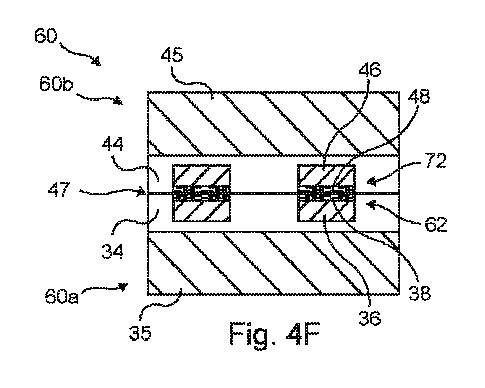
図4A~図4Fに、ある実施形態による、結合構造60を製造する製造工程の様々なステップを示す。図4Aにおいて、非導電性構造34にキャビティ32を形成することができる。図4Bにおいて、第1の堆積プロセスを使用してキャビティ32を第1の導電材料36で満たすことができる。第1の導電材料36は銅を含むことができる。いくつかの実施形態では、第1の導電材料36を、(例えば、2アンペア/平方デシメートル(ASD)未満の、さらに詳細には0.5ASD未満又は30mA/cm2未満の、さらに詳細には15mA/cm2未満の)比較的低い電流密度及び比較的低い堆積速度を使用するボトムアップ充填プロセスによってキャビティ32内にめっきすることができる。いくつかの実施形態では、キャビティ32を完全に第1の導電材料36で満たすことができる。通常は、キャビティ32を過度に満たし、CMPプロセスを採用して非導電材料34上から過度な導電材料を除去し、その後に過度な導電材料を除去又は平坦化して図4Bに示す構造を形成する。いくつかの実施形態では、第2の導電材料38の堆積前に第1の導電材料36の結晶粒を成長させて安定化させるために、第1の導電材料36をアニール処理することができる。
4A-4F illustrate various steps of a manufacturing process for producing a bonded
図4Cにおいて、第1の導電材料36の少なくとも一部を除去して開口部64を定めることができる。いくつかの実施形態では、エッチング(例えば、ウェットエッチング)によって第1の導電材料36を選択的に除去して、図2Cに示す第1の導電性フィーチャ36に凹部又は開口部64を形成することができる。いくつかの実施形態では、キャビティ32の表面上に少なくとも部分的にバリア層(図示せず)を設けることができる。バリア層の形成後に第1の導電材料36を提供して、キャビティ32の表面と第1の導電材料36との間にバリア層を介在させることができる。いくつかの実施形態では、バリア層を除去せずに第1の導電材料36の一部を選択的に除去することができる。非導電材料34のキャビティ32内に配置された第1の導電材料36の一部を除去することにより、凹部又は開口部64を形成することができる。凹部を有する第1の導電材料36は、結晶粒を拡大又は安定化させるためにアニール処理することができる。
4C, at least a portion of the first
図4Dにおいて、第2の堆積プロセスを使用して、キャビティ32内の第1の導電材料36上に第2の導電材料38を提供することができる。第2の導電材料38は銅を含むことができる。いくつかの実施形態では、第2の導電材料38を、低い添加剤濃度を使用して第1の堆積プロセスよりも高い堆積速度(高い電流密度)でめっきすることによって提供することができる。例えば、約2ASD以上などの比較的高い電流密度を採用して比較的微細な結晶粒を形成することができる。しかしながら、非常に高い電流密度での堆積は材料を粗く又は多孔質にする恐れがあるため、7ASD又は10ASDを上回るような非常に高い電流密度は好ましくない場合がある。いくつかの実施形態では、第1の堆積プロセスがめっきを含み、第2の堆積プロセスが化学蒸着(CVD)又は物理蒸着(PVD)などの蒸着を含む。異なるめっきプロセス又は蒸着プロセスのどちらによって形成されるかにかかわらず、第2の導電材料38の粒径は平均的に第1の導電材料36の粒径よりも観察可能なほど小さく、また第2の導電材料38では、結晶粒制御のためのめっき添加剤から存在するような不純物が第1の導電材料36と比べて観察可能なほど少ない。
In FIG. 4D, a second deposition process can be used to provide a second
非導電性構造34の少なくとも一部及び第2の導電材料38の少なくとも一部を含む表面を研磨し、処理して(例えば、活性化及び終端化して)素子(例えば、第1の素子60A)の結合面を定めることができる。いくつかの実施形態では、第2の導電材料38の表面が、非導電性構造34の表面と同一平面又は概ね同一平面であることができる。他のいくつかの実施形態では、上述したように、第2の導電材料38の表面を非導電性構造34の表面に対して凹ませることができる。
A surface including at least a portion of the
いくつかの実施形態では、この予備結合用の凹部が、非導電性結合面の下方75nm未満の、50nm未満の、好ましくは20nm未満の深さを有することができる。第2の導電材料38の厚みは、導電性フィーチャ62(第1の導電材料36と第2の導電材料38との組み合わせ)の厚みの70%未満、50%未満、30%未満、又は20%未満であることができる。いくつかの実施形態では、第2の導電材料38の厚みが30nm~600nmであることができ、第1の導電材料36の厚みが400nm~5000nmであることができる。いくつかの実施形態では、第2の導電材料38の厚みが50nmを上回ることができる。
In some embodiments, the pre-bonding recess can have a depth of less than 75 nm, less than 50 nm, and preferably less than 20 nm below the non-conductive bonding surface. The thickness of the second
図2Eにおいて、図2Dで形成された素子(第1の素子60a)を別の素子(第2の素子60b)に接触させることができる。第1の導電材料36は、第2の導電材料38の形成前にアニール処理することができるが、第2の導電材料38は、結合前にアニール処理せず、或いは上述したように第2の導電材料38の結晶粒が小さいままであるように、第1の導電材料のアニール処理と比べて低温及び/又は低時間でアニール処理することができる。第2の素子60bは、第1の素子60aと同一又は概ね同様の構造を有することができる。第1の素子60aを室温で第2の素子60bに接触させると、第1の素子60aの非導電性構造34及び第2の素子60bの非導電性構造44が結合界面47に沿って互いに結合することができる。いくつかの実施形態では、第1の素子60aを室温で第2の素子60bに接触させると、第1の素子60aの第2の導電材料38及び第2の素子60bの(第3の導電材料46及び第4の導電材料48を含むことができる)導電性フィーチャ72が結合界面47に沿って互いに結合することができる。図2Fにおいて、非導電性フィーチャ34、44の最初の室温での結合後に、接触した第1及び第2の素子60a、60bをアニール処理することができ、このような結合後のアニール処理によって導電性フィーチャ62、72が互いに膨張してハイブリッドボンディングが完了し、結合構造60を形成することができる。結合構造60では、第2の導電材料38の粒径が、第1の導電材料36の粒径よりも平均的に小さいままであることができる。
In FIG. 2E, the element formed in FIG. 2D (
図3A~図3E及び図4A~図4Fのコンポーネントは、例えば図1A及び図1Bのコンポーネントなどの本明細書に開示する同様のコンポーネントと同一又は概ね同様であることができる。例えば、非導電性フィーチャ42、52は、非導電性結合層108a、108bと同一又は概ね同様であることができ、デバイス部分35、45は、デバイス部分110a、110bと同一又は概ね同様であることができる。
The components of Figures 3A-3E and 4A-4F can be the same as or generally similar to similar components disclosed herein, such as the components of Figures 1A and 1B. For example, the non-conductive features 42, 52 can be the same as or generally similar to the
図3A~図3Eに示す実施形態及び図4A~図4Fに示す実施形態では、いずれも第2の導電材料38が小型の又は微細な結晶粒を含むことができる。第2の導電材料38の(垂直断面における横寸法で測定される)結合前の最大粒径は、導電性フィーチャ62の接触面の最大横寸法の20%未満、10%未満、5%未満、又は2%未満であることができる。結合界面における占有面積に関して言えば、結合前の結晶粒は、2000nm2未満、1000nm2未満、500nm2未満、300nm2未満、又は180nm2未満であることができる。横寸法において直線的に測定される第2の導電材料38の結合前の最大粒径は、500nm未満、200nm未満、100nm未満、50nm未満、25nm未満、20nm未満、又は15nm未満であることができる。例えば、第2の導電材料38における結晶粒の最大幅は、10nm~500nm、10nm~300nm、15nm~500nm、15nm~300nm、15nm~100nm、15nm~50nm、50nm~500nm、50nm~300nm、又は100nm~300nmの範囲内であることができる。
In both the embodiments shown in Figures 3A-3E and 4A-4F, the second
対照的に、下側の第1の導電材料36は、より大型の結晶粒を有することができる。例えば、側面積に関して言えば、第1の導電材料の結合前の結晶粒は、2000nm2超、4000nm2超、7000nm2超、又は10000nm2超であることができる。横寸法において直線的に測定される第1の導電材料の結合前の最大粒径は、50nm超、100nm超、300nm超、又は500nm超であることができる。結合前の第1の導電材料の平均サイズは、第2の導電材料の平均サイズよりも大きい。いくつかの実施形態では、第1の導電材料の平均サイズが、結合前及び結合後の両方において第2の導電材料の平均サイズよりも10%~200%大きいことができる。
In contrast, the lower first
上述したように、最初の結合後にアニール処理を行うことで、対向する素子30a、30b、60a、60bの導電性フィーチャ42、52、62、72を互いにさらに成長させてハイブリッドボンディングを完了することができる。このアニール処理は、第2の導電材料38の粒径も増大させるが、第2の導電材料38の第2の導電材料平均粒径は、下にある第1の導電材料36の平均導電材料粒径よりも小さいままである。第1及び第2の導電材料36、38は、いずれも大部分が同じ金属又は金属合金(例えば、銅)を含むことができるが、これらは、観察可能なほどに異なる平均及び最大粒径によって、またいくつかの実施形態では、第1の導電材料36における添加剤不純物が第2の導電材料38と比べて著しく多いことによって区別することができる。第2の導電材料38の粒径の結合前の最大横寸法は、200nm未満、150nm未満、100nm未満、50nm未満、又は20nm未満であることができる。第2の導電材料38の結合前の最大側断面積は、2000nm2未満、1000nm2未満、500nm2未満、300nm2未満、又は180nm2未満であることができる。第2の導電材料38の粒径の結合後の最大横寸法は、アニール処理中の結晶粒成長に起因して2μm未満、1μm未満、500nm未満、又は300nm未満であることができる。第2の導電材料38の結合後の最大側断面積は、4μm2未満、1μm2未満、250,000nm2未満であることができる。
As described above, an annealing process can be performed after the initial bonding to further grow the conductive features 42, 52, 62, 72 of the opposing
結晶粒はアニール処理中に成長するが、第2の導電材料38の結晶粒は導電性フィーチャ42、62に対して相対的に小さいままである。横寸法で直線的に測定される第2の導電材料38の最大粒径は、結合後の導電性フィーチャ42、62の幅の30%未満、20%未満、又は15%未満であることができ、ここでの粒径及びフィーチャサイズはいずれも横寸法で直線的に測定したものである。第2の導電材料38の小型の結晶粒は、結合界面47からの上位1~20の結晶粒層、さらに詳細には上位2~5の結晶粒層を表すことができるのに対し、結合界面47からさらに離れた結晶粒はより大型であり、より高い不純物濃度を含むことができる。結合後には、結合後の高温アニール処理の、例えば200℃以下の温度及び60分の結合時間という温度プロファイルに少なくとも部分的に依存して、第1の導電材料36の平均サイズが第2の導電材料38の平均サイズよりも大きいままであることができる。いくつかの実施形態では、結合後の第1の導電材料36の平均サイズが、第2の導電材料38の平均サイズよりも2~4倍大きいことができる。
Although the grains grow during the annealing process, the grains of the second
図5は、第1の導電材料36及び第2の導電材料38を含む導電性フィーチャ42がどのように見えるかを示すために生成した画像である。図6は、第1の導電材料36及び第2の導電材料38を含む導電性フィーチャ62がどのように見えるかを示すために生成した画像である。図5及び図6は、第1及び第2の導電材料36、38の粒径が目に見えて異なることを示す。当業者であれば、導電性フィーチャ42、62は、それぞれ大型の結晶粒を含む部分(例えば、第1の導電材料36)と、小型の結晶粒を含む目に見えて顕著な部分(例えば、第2の導電材料38)とを含むことが分かるであろう。
5 is an image generated to show how a
1つの態様では、素子の形成方法を開示する。方法は、非導電性構造を準備することと、非導電性構造にキャビティを形成することと、を含むことができる。キャビティは、非導電性構造の表面から非導電性構造の厚みを少なくとも部分的に貫通する。方法は、第1の導電材料と、第1の導電材料上の第2の導電材料とをキャビティ内に含む導電性フィーチャを提供することを含むことができる。第2の導電材料は素子の結合面に配置される。第2の導電材料の直線横寸法での最大粒径は、導電性フィーチャの直線横寸法の20%よりも小さい。方法は、素子の結合面をダイレクトボンディングのために調製することを含むことができる。 In one aspect, a method of forming an element is disclosed. The method can include providing a non-conductive structure and forming a cavity in the non-conductive structure. The cavity extends at least partially through a thickness of the non-conductive structure from a surface of the non-conductive structure. The method can include providing a conductive feature including a first conductive material in the cavity and a second conductive material on the first conductive material. The second conductive material is disposed on a bonding surface of the element. A maximum grain size in a linear lateral dimension of the second conductive material is less than 20% of a linear lateral dimension of the conductive feature. The method can include preparing the bonding surface of the element for direct bonding.
1つの実施形態では、第2の導電材料の結晶粒界に20パーツパーミリオン(ppm)未満の不純物が存在する。 In one embodiment, the second conductive material has less than 20 parts per million (ppm) of impurities at its grain boundaries.
1つの実施形態では、第2の導電材料の平均粒径が第1の導電材料の平均粒径よりも小さい。 In one embodiment, the average particle size of the second conductive material is smaller than the average particle size of the first conductive material.
1つの実施形態では、導電性のフィーチャを提供することが、第1の導電材料及び第2の導電材料を別々に提供することを含む。第1の導電材料を提供することは、キャビティを部分的に満たすことを含むことができる。第1の導電材料を提供することは、キャビティを第1の導電材料で満たし、第1の導電材料の一部を除去することを含むことができる。方法は、第2の導電材料を提供する前に第1の導電材料をアニール処理することをさらに含むことができる。導電材料を提供することは、第2の導電材料をプラズマ蒸着(PVD)によって第1の導電材料上に提供することを含むことができる。第2の導電材料は、第1の導電材料を提供する第1の堆積プロセスよりも高い電流密度でのめっきによって提供することができる。結合面を調製することは、非導電材料及び第2の導電材料の表面を研磨することを含むことができる。 In one embodiment, providing the conductive feature includes separately providing a first conductive material and a second conductive material. Providing the first conductive material can include partially filling the cavity. Providing the first conductive material can include filling the cavity with the first conductive material and removing a portion of the first conductive material. The method can further include annealing the first conductive material before providing the second conductive material. Providing the conductive material can include providing the second conductive material on the first conductive material by plasma vapor deposition (PVD). The second conductive material can be provided by plating at a higher current density than the first deposition process that provides the first conductive material. Preparing the bonding surface can include polishing the surfaces of the non-conductive material and the second conductive material.
1つの実施形態では、第2の導電材料の最大粒径が、導電性フィーチャの直線横寸法の10%よりも小さい。第2の導電材料の最大粒径は、導電性フィーチャの直線横寸法の5%よりも小さいことができる。第2の導電材料の最大粒径は、導電性フィーチャの直線横寸法の2%よりも小さいことができる。 In one embodiment, the maximum grain size of the second conductive material is less than 10% of the linear lateral dimension of the conductive feature. The maximum grain size of the second conductive material can be less than 5% of the linear lateral dimension of the conductive feature. The maximum grain size of the second conductive material can be less than 2% of the linear lateral dimension of the conductive feature.
1つの実施形態では、結合面における導電性フィーチャの面積が7μm2よりも小さい。 In one embodiment, the area of the conductive features on the bonding surface is less than 7 μm 2 .
1つの実施形態では、結合面における第2の導電材料の断面図での最大結晶粒側面積が2000nm2よりも小さい。 In one embodiment, the maximum grain lateral area in cross section of the second conductive material at the bonding surface is less than 2000 nm 2 .
つの実施形態では、結合面における第2の導電材料の最大直線横方向粒径が200nmよりも小さい。 In one embodiment, the maximum linear lateral grain size of the second conductive material at the bonding surface is less than 200 nm.
1つの実施形態では、第1の導電材料及び第2の導電材料が銅を含む。 In one embodiment, the first conductive material and the second conductive material include copper.
1つの実施形態では、方法が、第1の導電材料と第2の導電材料との間に介在層を設けることをさらに含む。 In one embodiment, the method further includes providing an intervening layer between the first conductive material and the second conductive material.
1つの実施形態では、第2の導電材料の厚みが導電性フィーチャの厚みの50%未満である。第2の導電材料の厚みは、導電性フィーチャの厚みの30%未満であることができる。 In one embodiment, the thickness of the second conductive material is less than 50% of the thickness of the conductive feature. The thickness of the second conductive material can be less than 30% of the thickness of the conductive feature.
1つの態様では、結合構造の形成方法を開示する。方法は、非導電性結合面を有する第1の非導電性構造と、非導電性結合面から非導電性構造の厚みを少なくとも部分的に貫通するキャビティと、キャビティ内に配置された第1の導電材料及び第1の導電材料上の第2の導電材料を有する第1の導電性フィーチャとを含む第1の素子を準備することを含むことができる。第2の導電材料は、素子の結合面において少なくとも部分的に露出する。第2の導電材料の平均粒径は、第1の導電材料の平均粒径よりも小さい。方法は、第2の非導電性構造と第2の導電性フィーチャとを含む第2の素子を準備することを含むことができる。方法は、第2の導電材料にアニールプロセスを行うことなく、第1の素子の結合面と第2の素子の結合面とを接触させることと、接触後に第1の素子と第2の素子とを直接結合することと、を含むことができる。 In one aspect, a method of forming a bonded structure is disclosed. The method can include providing a first element including a first non-conductive structure having a non-conductive bonding surface, a cavity extending at least partially through a thickness of the non-conductive structure from the non-conductive bonding surface, and a first conductive feature having a first conductive material disposed in the cavity and a second conductive material on the first conductive material. The second conductive material is at least partially exposed at the bonding surface of the element. The average grain size of the second conductive material is smaller than the average grain size of the first conductive material. The method can include providing a second element including a second non-conductive structure and a second conductive feature. The method can include contacting the bonding surface of the first element with the bonding surface of the second element without performing an annealing process on the second conductive material, and directly bonding the first element with the second element after contacting.
1つの実施形態では、第2の導電材料の結晶粒界に20パーツパーミリオン(ppm)未満の不純物が存在する。 In one embodiment, the second conductive material has less than 20 parts per million (ppm) of impurities at its grain boundaries.
1つの実施形態では、第1の素子と第2の素子とを直接結合することが、介在接着剤を使用せずに第1の非導電性構造と第2の非導電性構造とを直接結合し、介在接着剤を使用せずに第1の導電性フィーチャと第2の導電性フィーチャとを直接結合することを含む。 In one embodiment, directly bonding the first element to the second element includes directly bonding the first non-conductive structure to the second non-conductive structure without the use of an intervening adhesive, and directly bonding the first conductive feature to the second conductive feature without the use of an intervening adhesive.
1つの実施形態では、第1の素子を準備することが、第1の非導電性構造を準備することと、第1の非導電性構造にキャビティを形成することと、第1の導電材料を提供することと、第1の導電材料を提供した後に第2の導電材料を提供することと、を含む。方法は、第2の導電材料を提供する前に第1の導電材料をアニール処理することをさらに含むことができる。 In one embodiment, preparing the first element includes providing a first non-conductive structure, forming a cavity in the first non-conductive structure, providing a first conductive material, and providing a second conductive material after providing the first conductive material. The method may further include annealing the first conductive material before providing the second conductive material.
1つの実施形態では、方法が、結合された第1及び第2の素子をアニール処理することをさらに含む。 In one embodiment, the method further includes annealing the bonded first and second elements.
1つの実施形態では、方法が、素子の結合面をダイレクトボンディングのために調製することをさらに含む。結合面を調製することは、非導電材料及び第2の導電材料の表面を研磨することを含むことができる。 In one embodiment, the method further includes preparing a bonding surface of the element for direct bonding. Preparing the bonding surface may include polishing the surfaces of the non-conductive material and the second conductive material.
1つの実施形態では、第1の素子と第2の素子とを直接結合する前の第2の導電材料の直線横寸法での最大粒径が、導電性フィーチャの直線横寸法の20%よりも小さい。第1の素子と第2の素子とを直接結合する前の第2の導電材料の最大粒径は、導電性フィーチャの直線横寸法の10%よりも小さいことができる。第1の素子と第2の素子とを直接結合する前の第2の導電材料の最大粒径は、導電性フィーチャの直線横寸法の5%よりも小さいことができる。 In one embodiment, the maximum grain size in a linear lateral dimension of the second conductive material prior to directly bonding the first element and the second element is less than 20% of the linear lateral dimension of the conductive feature. The maximum grain size of the second conductive material prior to directly bonding the first element and the second element can be less than 10% of the linear lateral dimension of the conductive feature. The maximum grain size of the second conductive material prior to directly bonding the first element and the second element can be less than 5% of the linear lateral dimension of the conductive feature.
1つの実施形態では、導電性フィーチャの露出した面積全体が7μm2よりも小さい。 In one embodiment, the total exposed area of the conductive features is less than 7 μm 2 .
1つの実施形態では、第1の素子と第2の素子とを直接結合する前の第2の導電材料の最大結晶粒側面積が2000nm2よりも小さい。 In one embodiment, the maximum grain lateral area of the second conductive material prior to direct bonding of the first element and the second element is less than 2000 nm 2 .
1つの実施形態では、第1の素子と第2の素子とを直接結合する前の第2の導電材料の最大線横方向粒径が200nmよりも小さい。 In one embodiment, the maximum linear lateral grain size of the second conductive material prior to direct bonding of the first element and the second element is less than 200 nm.
1つの実施形態では、第1の素子と第2の素子とを直接結合した後の第2の導電材料の直線横寸法での最大粒径が、導電性フィーチャの直線横寸法の30%よりも小さい。第1の素子と第2の素子とを直接結合した後の第2の導電材料の最大粒径は、導電性フィーチャの直線横寸法の20%よりも小さいことができる。第1の素子と第2の素子とを直接結合した後の第2の導電材料の最大粒径は、導電性フィーチャの直線横寸法の15%よりも小さいことができる。 In one embodiment, the maximum grain size in a linear lateral dimension of the second conductive material after directly bonding the first element and the second element is less than 30% of the linear lateral dimension of the conductive feature. The maximum grain size of the second conductive material after directly bonding the first element and the second element can be less than 20% of the linear lateral dimension of the conductive feature. The maximum grain size of the second conductive material after directly bonding the first element and the second element can be less than 15% of the linear lateral dimension of the conductive feature.
1つの実施形態では、第1の素子と第2の素子とを直接結合した後の結合面における第2の導電材料の最大結晶粒側面積が71000nm2よりも小さい。 In one embodiment, the maximum grain lateral area of the second conductive material at the bonding surface after direct bonding of the first element and the second element is less than 71000 nm2 .
1つの実施形態では、第1の素子と第2の素子とを直接結合した後の結合面における第2の導電材料の最大直線横方向粒径が2μmよりも小さい。 In one embodiment, the maximum linear lateral grain size of the second conductive material at the bonding surface after direct bonding of the first element and the second element is less than 2 μm.
1つの実施形態では、第1の導電材料及び第2の導電材料が銅を含む。 In one embodiment, the first conductive material and the second conductive material include copper.
1つの実施形態では、方法が、第1の導電材料と第2の導電材料との間に介在層を設けることをさらに含む。 In one embodiment, the method further includes providing an intervening layer between the first conductive material and the second conductive material.
1つの態様では、素子を開示する。素子は、非導電性構造と、非導電性構造内のキャビティとを含むことができる。キャビティは、非導電性構造の表面から非導電性構造の厚みを少なくとも部分的に貫通する。素子は、第1の導電材料と、第1の導電材料上の第2の導電材料とを含む導電性フィーチャをキャビティ内に含むことができる。第2の導電材料は素子の結合面に配置される。第2の導電材料の直線横寸法での最大粒径は、導電性フィーチャの直線横寸法の20%よりも小さい。 In one aspect, an element is disclosed. The element can include a non-conductive structure and a cavity in the non-conductive structure. The cavity extends at least partially through a thickness of the non-conductive structure from a surface of the non-conductive structure. The element can include a conductive feature in the cavity including a first conductive material and a second conductive material on the first conductive material. The second conductive material is disposed on a bonding surface of the element. The second conductive material has a maximum grain size in a linear lateral dimension that is less than 20% of the linear lateral dimension of the conductive feature.
1つの実施形態では、第2の導電材料の結晶粒界に20パーツパーミリオン(ppm)未満の不純物が存在する。 In one embodiment, the second conductive material has less than 20 parts per million (ppm) of impurities at its grain boundaries.
1つの実施形態では、第2の導電材料の直線横寸法での平均粒径は、第1の導電材料の直線横寸法での平均粒径よりも小さい。 In one embodiment, the average particle size in a linear lateral dimension of the second conductive material is smaller than the average particle size in a linear lateral dimension of the first conductive material.
1つの実施形態では、第2の導電材料の厚みが導電性フィーチャの厚みの50%未満である。第2の導電材料の厚みは、導電性フィーチャの厚みの30%未満であることができる。 In one embodiment, the thickness of the second conductive material is less than 50% of the thickness of the conductive feature. The thickness of the second conductive material can be less than 30% of the thickness of the conductive feature.
1つの実施形態では、素子の結合面がダイレクトボンディングのために調製される。結合面は、2nm未満の二乗平均平方根(rms)表面粗さを有することができる。 In one embodiment, the bonding surface of the component is prepared for direct bonding. The bonding surface can have a root mean square (rms) surface roughness of less than 2 nm.
1つの実施形態では、第2の導電材料の最大粒径が、導電性フィーチャの直線横寸法の10%よりも小さい。第2の導電材料の最大粒径は、導電性フィーチャの直線横寸法の5%よりも小さいことができる。第2の導電材料の最大粒径は、導電性フィーチャの直線横寸法の2%よりも小さいことができる。 In one embodiment, the maximum grain size of the second conductive material is less than 10% of the linear lateral dimension of the conductive feature. The maximum grain size of the second conductive material can be less than 5% of the linear lateral dimension of the conductive feature. The maximum grain size of the second conductive material can be less than 2% of the linear lateral dimension of the conductive feature.
1つの実施形態では、結合面における導電性フィーチャの直線横寸法が7μm2よりも小さい。 In one embodiment, the conductive features have a linear lateral dimension at the bonding surface that is less than 7 μm 2 .
1つの実施形態では、結合面における第2の導電材料の最大結晶粒側面積が2000nm2よりも小さい。 In one embodiment, the maximum grain lateral area of the second conductive material at the bonding surface is less than 2000 nm2 .
1つの実施形態では、結合面における第2の導電材料の最大粒径が200nmよりも小さい。 In one embodiment, the maximum particle size of the second conductive material at the bonding surface is less than 200 nm.
1つの実施形態では、第1の導電材料及び第2の導電材料が銅を含む。 In one embodiment, the first conductive material and the second conductive material include copper.
1つの実施形態では、素子が、第1の導電材料と第2の導電材料との間に介在層をさらに含む。 In one embodiment, the element further includes an intervening layer between the first conductive material and the second conductive material.
1つの態様では、結合構造を開示する。結合構造は、非導電性結合面を有する第1の非導電性構造と、非導電性結合面から非導電性構造の厚みを少なくとも部分的に貫通するキャビティと、キャビティ内に配置された第1の導電材料及び第1の導電材料上の第2の導電材料を有する第1の導電性フィーチャとを含む第1の素子を含むことができる。第2の導電材料の平均粒径は、第1の導電材料の平均粒径よりも小さい。第2の導電材料の結晶粒界に20パーツパーミリオン(ppm)未満の不純物が存在する。結合構造は、第2の非導電性構造と第2の導電性フィーチャとを含む第2の素子を含むことができる。第1の素子及び第2の素子は、第1の非導電性構造と第2の非導電性構造とが介在接着剤を使用せずに直接結合されるように互いに結合される。第2の導電材料及び第2の導電性フィーチャは、介在接着剤を使用せずに互いに直接結合される。 In one aspect, a bonded structure is disclosed. The bonded structure can include a first element including a first non-conductive structure having a non-conductive bonding surface, a cavity extending at least partially through a thickness of the non-conductive structure from the non-conductive bonding surface, and a first conductive feature having a first conductive material disposed in the cavity and a second conductive material on the first conductive material. The average grain size of the second conductive material is smaller than the average grain size of the first conductive material. The second conductive material has less than 20 parts per million (ppm) of impurities at its grain boundaries. The bonded structure can include a second element including a second non-conductive structure and a second conductive feature. The first element and the second element are bonded together such that the first non-conductive structure and the second non-conductive structure are directly bonded together without the use of an intervening adhesive. The second conductive material and the second conductive feature are directly bonded together without the use of an intervening adhesive.
1つの実施形態では、第2の導電材料の厚みが導電性フィーチャの厚みの50%未満である。第2の導電材料の厚みは、導電性フィーチャの厚みの30%未満である。 In one embodiment, the thickness of the second conductive material is less than 50% of the thickness of the conductive feature. The thickness of the second conductive material is less than 30% of the thickness of the conductive feature.
1つの実施形態では、第1の導電材料及び第2の導電材料が銅を含む。 In one embodiment, the first conductive material and the second conductive material include copper.
1つの実施形態では、結合構造が、第1の導電材料と第2の導電材料との間に介在層をさらに含む。 In one embodiment, the bond structure further includes an intervening layer between the first conductive material and the second conductive material.
1つの実施形態では、第1の素子と第2の素子とを直接結合した後の第2の導電材料の直線横寸法での最大粒径が、導電性フィーチャの直線横寸法の30%よりも小さい。第1の素子と第2の素子とを直接結合した後の第2の導電材料の最大粒径は、導電性フィーチャの直線横寸法の20%よりも小さいことができる。第1の素子と第2の素子とを直接結合した後の第2の導電材料の最大粒径は、導電性フィーチャの直線横寸法の15%よりも小さいことができる。 In one embodiment, the maximum grain size in a linear lateral dimension of the second conductive material after directly bonding the first element and the second element is less than 30% of the linear lateral dimension of the conductive feature. The maximum grain size of the second conductive material after directly bonding the first element and the second element can be less than 20% of the linear lateral dimension of the conductive feature. The maximum grain size of the second conductive material after directly bonding the first element and the second element can be less than 15% of the linear lateral dimension of the conductive feature.
1つの実施形態では、第1の素子と第2の素子とを直接結合した後の結合面における第2の導電材料の最大結晶粒側面積が71000nm2よりも小さい。 In one embodiment, the maximum grain lateral area of the second conductive material at the bonding surface after direct bonding of the first element and the second element is less than 71000 nm2 .
1つの実施形態では、第1の素子と第2の素子とを直接結合した後の第2の導電材料の最大直線横方向粒径が2μmよりも小さい。 In one embodiment, the maximum linear lateral grain size of the second conductive material after direct bonding of the first element and the second element is less than 2 μm.
1つの態様では、素子の形成方法を開示する。方法は、非導電性構造を提供することと、非導電性構造にキャビティを形成することと、第1の導電材料及び第1の導電材料上の第2の導電材料をキャビティ内に含む導電性フィーチャを、第2の導電材料が素子の結合面において少なくとも部分的に露出するように提供することと、を含むことができる。第2の導電材料の結晶粒界には20パーツパーミリオン(ppm)未満の不純物が存在し、第2の導電材料の直線横寸法での最大粒径は、導電性フィーチャの直線横寸法の20%よりも小さい。 In one aspect, a method of forming an element is disclosed. The method can include providing a non-conductive structure, forming a cavity in the non-conductive structure, and providing a conductive feature including a first conductive material and a second conductive material on the first conductive material in the cavity such that the second conductive material is at least partially exposed at a bonding surface of the element. The second conductive material has less than 20 parts per million (ppm) of impurities at grain boundaries, and the second conductive material has a maximum grain size in a linear lateral dimension that is less than 20% of the linear lateral dimension of the conductive feature.
1つの実施形態では、導電性フィーチャを提供することが、第1の導電材料及び第2の導電材料を別々に提供することを含む。第1の導電材料を提供することは、キャビティを部分的に満たすことを含むことができる。第1の導電材料を提供することは、キャビティを第1の導電材料で満たし、第1の導電材料の一部を除去することを含むことができる。方法は、第2の導電材料を提供する前に第1の導電材料をアニール処理することをさらに含むことができる。導電材料を提供することは、蒸着によって第1の導電材料上に第2の導電材料を提供することを含むことができる。蒸着は、物理蒸着又は化学蒸着であることができる。第2の導電材料は、第1の導電材料を提供する第1の堆積プロセスよりも高い電流密度でのめっきによって提供することができる。 In one embodiment, providing the conductive feature includes separately providing a first conductive material and a second conductive material. Providing the first conductive material can include partially filling the cavity. Providing the first conductive material can include filling the cavity with the first conductive material and removing a portion of the first conductive material. The method can further include annealing the first conductive material before providing the second conductive material. Providing the conductive material can include providing the second conductive material on the first conductive material by vapor deposition. The vapor deposition can be physical vapor deposition or chemical vapor deposition. The second conductive material can be provided by plating at a higher current density than the first deposition process that provides the first conductive material.
1つの実施形態では、方法が、素子の結合面をダイレクトボンディングのために調製することをさらに含む。結合面を調製することは、非導電材料及び第2の導電材料の表面を研磨することを含むことができる。第2の導電材料の最大粒径は、導電性フィーチャの直線横寸法の5%よりも小さいことができる。第2の導電材料の最大粒径は、導電性フィーチャの直線横寸法の2%よりも小さいことができる。 In one embodiment, the method further includes preparing a bonding surface of the element for direct bonding. Preparing the bonding surface can include polishing the surfaces of the non-conductive material and the second conductive material. The maximum grain size of the second conductive material can be less than 5% of a linear lateral dimension of the conductive feature. The maximum grain size of the second conductive material can be less than 2% of a linear lateral dimension of the conductive feature.
1つの実施形態では、導電性フィーチャの露出した面積全体が7μm2よりも小さい。 In one embodiment, the total exposed area of the conductive features is less than 7 μm 2 .
1つの実施形態では、結合面における第2の導電材料の最大結晶粒側面積が2000nm2よりも小さい。 In one embodiment, the maximum grain lateral area of the second conductive material at the bonding surface is less than 2000 nm2 .
1つの実施形態では、第2の導電材料の最大粒径が200nmよりも小さい。 In one embodiment, the maximum particle size of the second conductive material is less than 200 nm.
1つの実施形態では、第1の導電材料及び第2の導電材料が銅を含む。 In one embodiment, the first conductive material and the second conductive material include copper.
1つの実施形態では、方法が、第1の導電材料と第2の導電材料との間に介在層を設けることをさらに含む。 In one embodiment, the method further includes providing an intervening layer between the first conductive material and the second conductive material.
1つの実施形態では、第2の導電材料の厚みが、導電性フィーチャの厚みの50%未満である。第2の導電材料の厚みは、導電性フィーチャの厚みの30%未満である。 In one embodiment, the thickness of the second conductive material is less than 50% of the thickness of the conductive feature. The thickness of the second conductive material is less than 30% of the thickness of the conductive feature.
1つの態様では、結合構造の形成方法を開示する。方法は、非導電性結合面を有する第1の非導電性構造と、非導電性構造内のキャビティと、キャビティ内に配置された第1の導電材料及び第1の導電材料上の第2の導電材料を有する第1の導電性フィーチャとを含む第1の素子を準備することを含むことができる。第2の導電材料は、素子の結合面において少なくとも部分的に露出する。第2の導電材料の結晶粒界には20パーツパーミリオン(ppm)未満の不純物が存在する。第2の導電材料の直線横寸法での最大粒径は、導電性フィーチャの直線横寸法の20%よりも小さい。方法は、第2の非導電性構造と第2の導電性フィーチャとを含む第2の素子を準備することを含むことができる。方法は、第2の導電材料にアニールプロセスを行うことなく第1の素子の結合面と第2の素子の結合面とを接触させ、接触後に第1の素子と第2の素子とを直接結合することを含むことができる。 In one aspect, a method of forming a bonded structure is disclosed. The method can include providing a first element including a first non-conductive structure having a non-conductive bonding surface, a cavity in the non-conductive structure, and a first conductive feature having a first conductive material disposed in the cavity and a second conductive material on the first conductive material. The second conductive material is at least partially exposed at the bonding surface of the element. The second conductive material has less than 20 parts per million (ppm) of impurities at grain boundaries. The second conductive material has a maximum grain size in a linear lateral dimension that is less than 20% of the linear lateral dimension of the conductive feature. The method can include providing a second element including a second non-conductive structure and a second conductive feature. The method can include contacting the bonding surface of the first element with the bonding surface of the second element without performing an annealing process on the second conductive material, and directly bonding the first element with the second element after contacting.
1つの実施形態では、第1の素子と第2の素子とを直接結合することが、介在接着剤を使用せずに第1の非導電性構造と第2の非導電性構造とを直接結合し、介在接着剤を使用せずに第1の導電性フィーチャと第2の導電性フィーチャとを直接結合することを含む。 In one embodiment, directly bonding the first element to the second element includes directly bonding the first non-conductive structure to the second non-conductive structure without the use of an intervening adhesive, and directly bonding the first conductive feature to the second conductive feature without the use of an intervening adhesive.
1つの実施形態では、第1の素子を準備することが、第1の非導電性構造を準備することと、第1の非導電性構造にキャビティを形成することと、第1の導電材料を提供することと、第1の導電材料を提供した後に第2の導電材料を提供することと、を含む。方法は、第2の導電材料を提供する前に第1の導電材料をアニール処理することをさらに含むことができる。 In one embodiment, preparing the first element includes providing a first non-conductive structure, forming a cavity in the first non-conductive structure, providing a first conductive material, and providing a second conductive material after providing the first conductive material. The method may further include annealing the first conductive material before providing the second conductive material.
1つの実施形態では、方法が、結合された第1及び第2の素子をアニール処理することをさらに含む。 In one embodiment, the method further includes annealing the bonded first and second elements.
1つの実施形態では、方法は、素子の結合面をダイレクトボンディングのために調製することをさらに含む。結合面を調製することは、非導電材料及び第2の導電材料の表面を研磨することを含むことができる。 In one embodiment, the method further includes preparing a bonding surface of the element for direct bonding. Preparing the bonding surface may include polishing the surfaces of the non-conductive material and the second conductive material.
1つの実施形態では、第1の素子と第2の素子とを直接結合する前の第2の導電材料の最大粒径が、導電性フィーチャの直線横寸法の5%よりも小さい。第1の素子と第2の素子とを直接結合する前の第2の導電材料の最大粒径は、導電性フィーチャの直線横寸法の2%よりも小さいことができる。 In one embodiment, the maximum grain size of the second conductive material prior to directly bonding the first and second elements is less than 5% of the linear lateral dimension of the conductive feature. The maximum grain size of the second conductive material prior to directly bonding the first and second elements can be less than 2% of the linear lateral dimension of the conductive feature.
1つの実施形態では、導電性フィーチャの露出した面積全体が7μm2よりも小さい。 In one embodiment, the total exposed area of the conductive features is less than 7 μm 2 .
1つの実施形態では、第1の素子と第2の素子とを直接結合する前の結合面における第2の導電材料の最大結晶粒側面積が2000nm2よりも小さい。 In one embodiment, the maximum grain lateral area of the second conductive material at the bonding surface prior to direct bonding of the first element and the second element is less than 2000 nm 2 .
1つの実施形態では、第1の素子と第2の素子とを直接結合する前の第2の導電材料の最大粒径が200nmよりも小さい。 In one embodiment, the maximum particle size of the second conductive material prior to direct bonding of the first element and the second element is less than 200 nm.
1つの実施形態では、第1の素子と第2の素子とを直接結合した後の第2の導電材料の最大粒径が、導電性フィーチャの直線横寸法の30%よりも小さい。第1の素子と第2の素子とを直接結合した後の第2の導電材料の最大粒径は、導電性フィーチャの直線横寸法の20%よりも小さいことができる。第1の素子と第2の素子とを直接結合した後の第2の導電材料の最大粒径は、導電性フィーチャの直線横寸法の15%よりも小さいことができる。 In one embodiment, the maximum grain size of the second conductive material after directly bonding the first element and the second element is less than 30% of the linear lateral dimension of the conductive feature. The maximum grain size of the second conductive material after directly bonding the first element and the second element can be less than 20% of the linear lateral dimension of the conductive feature. The maximum grain size of the second conductive material after directly bonding the first element and the second element can be less than 15% of the linear lateral dimension of the conductive feature.
1つの実施形態では、第1の素子と第2の素子とを直接結合した後の結合面における第2の導電材料の最大結晶粒側面積が71000nm2よりも小さい。 In one embodiment, the maximum grain lateral area of the second conductive material at the bonding surface after direct bonding of the first element and the second element is less than 71000 nm2 .
1つの実施形態では、第1の素子と第2の素子とを直接結合した後の第2の導電材料の最大粒径が2μmよりも小さい。 In one embodiment, the maximum particle size of the second conductive material after directly bonding the first element and the second element is less than 2 μm.
1つの実施形態では、第1の導電材料及び第2の導電材料が銅を含む。 In one embodiment, the first conductive material and the second conductive material include copper.
1つの実施形態では、方法が、第1の導電材料と第2の導電材料との間に介在層を設けることをさらに含む。 In one embodiment, the method further includes providing an intervening layer between the first conductive material and the second conductive material.
1つの態様では、素子を開示する。素子は、非導電性構造と、非導電性構造内のキャビティとを含むことができる。キャビティは、非導電性構造の表面から非導電性構造の厚みを少なくとも部分的に貫通する。素子は、第1の導電材料と、第1の導電材料上の第2の導電材料とをキャビティ内に含む導電性フィーチャを含むことができる。第2の導電材料は、素子の結合面に配置される。第2の導電材料の直線横寸法での最大粒径は、導電性フィーチャの直線横寸法の20%よりも小さい。第2の導電材料の結晶粒界には20パーツパーミリオン(ppm)未満の不純物が存在する。 In one aspect, an element is disclosed. The element can include a non-conductive structure and a cavity in the non-conductive structure. The cavity extends at least partially through a thickness of the non-conductive structure from a surface of the non-conductive structure. The element can include a conductive feature including a first conductive material in the cavity and a second conductive material on the first conductive material. The second conductive material is disposed on a bonding surface of the element. The second conductive material has a maximum grain size in a linear lateral dimension that is less than 20% of the linear lateral dimension of the conductive feature. The second conductive material has less than 20 parts per million (ppm) of impurities at grain boundaries.
1つの実施形態では、第2の導電材料の厚みが、導電性フィーチャの厚みの50%未満である。第2の導電材料の厚みは、導電性フィーチャの厚みの30%未満であることができる。 In one embodiment, the thickness of the second conductive material is less than 50% of the thickness of the conductive feature. The thickness of the second conductive material can be less than 30% of the thickness of the conductive feature.
1つの実施形態では、素子の結合面がダイレクトボンディングのために調製される。結合面は、2nm未満の二乗平均平方根(rms)表面粗さを有することができる。 In one embodiment, the bonding surface of the component is prepared for direct bonding. The bonding surface can have a root mean square (rms) surface roughness of less than 2 nm.
1つの実施形態では、第2の導電材料の最大粒径が、導電性フィーチャの直線横寸法の5%よりも小さい。第2の導電材料の最大粒径は、導電性フィーチャの直線横寸法の2%よりも小さいことができる。 In one embodiment, the maximum grain size of the second conductive material is less than 5% of the linear lateral dimension of the conductive feature. The maximum grain size of the second conductive material can be less than 2% of the linear lateral dimension of the conductive feature.
1つの実施形態では、結合面における導電性フィーチャの面積が7μm2よりも小さい。 In one embodiment, the area of the conductive features on the bonding surface is less than 7 μm 2 .
1つの実施形態では、結合面における第2の導電材料の最大結晶粒側面積が2000nm2よりも小さい。 In one embodiment, the maximum grain lateral area of the second conductive material at the bonding surface is less than 2000 nm2 .
1つの実施形態では、第2の導電材料の最大粒径が200nmよりも小さい。 In one embodiment, the maximum particle size of the second conductive material is less than 200 nm.
1つの実施形態では、第1の導電材料及び第2の導電材料が銅を含む。 In one embodiment, the first conductive material and the second conductive material include copper.
1つの実施形態では、素子が、第1の導電材料と第2の導電材料との間に介在層をさらに含む。 In one embodiment, the element further includes an intervening layer between the first conductive material and the second conductive material.
1つの態様では、結合構造を開示する。結合構造は、非導電性結合面を有する第1の非導電性構造と、非導電性結合面から非導電性構造の厚みを少なくとも部分的に貫通するキャビティと、キャビティ内に配置された第1の導電材料及び第1の導電材料上の第2の導電材料を有する第1の導電性フィーチャとを含む第1の素子を含むことができる。結合構造は、第2の非導電性構造と第2の導電性フィーチャとを含む第2の素子を含むことができる。第1の素子及び第2の素子は、第1の非導電性構造と第2の非導電性構造とが介在接着剤を使用せずに互いに直接結合され、第2の導電材料と第2の導電性フィーチャとが介在接着剤を使用せずに互いに直接結合されるように互いに結合される。第1の素子と第2の素子とを直接結合した後の第2の導電材料の直線横寸法での最大粒径は、導電性フィーチャの直線横寸法の30%よりも小さい。 In one aspect, a bonded structure is disclosed. The bonded structure can include a first element including a first non-conductive structure having a non-conductive bonding surface, a cavity extending at least partially through a thickness of the non-conductive structure from the non-conductive bonding surface, and a first conductive feature having a first conductive material disposed in the cavity and a second conductive material on the first conductive material. The bonded structure can include a second element including a second non-conductive structure and a second conductive feature. The first element and the second element are bonded together such that the first non-conductive structure and the second non-conductive structure are directly bonded together without the use of an intervening adhesive, and the second conductive material and the second conductive feature are directly bonded together without the use of an intervening adhesive. The second conductive material has a maximum grain size in a linear lateral dimension after directly bonding the first element and the second element is less than 30% of the linear lateral dimension of the conductive feature.
1つの実施形態では、第2の導電材料の結晶粒界に20パーツパーミリオン(ppm)未満の不純物が存在する。 In one embodiment, the second conductive material has less than 20 parts per million (ppm) of impurities at its grain boundaries.
1つの実施形態では、第2の導電材料の厚みが、導電性フィーチャの厚みの50%未満である。第2の導電材料の厚みは、導電性フィーチャの厚みの30%未満である。 In one embodiment, the thickness of the second conductive material is less than 50% of the thickness of the conductive feature. The thickness of the second conductive material is less than 30% of the thickness of the conductive feature.
1つの実施形態では、第1の導電材料及び第2の導電材料が銅を含む。 In one embodiment, the first conductive material and the second conductive material include copper.
1つの実施形態では、結合構造が、第1の導電材料と第2の導電材料との間に介在層をさらに含む。 In one embodiment, the bond structure further includes an intervening layer between the first conductive material and the second conductive material.
1つの実施形態では、第1の素子と第2の素子とを直接結合した後の第2の導電材料の最大粒径が、導電性フィーチャの直線横寸法の20%よりも小さい。第1の素子と第2の素子とを直接結合した後の第2の導電材料の最大粒径は、導電性フィーチャの直線横寸法の15%よりも小さいことができる。 In one embodiment, the maximum grain size of the second conductive material after directly bonding the first element and the second element is less than 20% of the linear lateral dimension of the conductive feature. The maximum grain size of the second conductive material after directly bonding the first element and the second element can be less than 15% of the linear lateral dimension of the conductive feature.
1つの実施形態では、第1の素子と第2の素子とを直接結合した後の結合面における第2の導電材料の最大結晶粒側面積が71000nm2よりも小さい。 In one embodiment, the maximum grain lateral area of the second conductive material at the bonding surface after direct bonding of the first element and the second element is less than 71000 nm2 .
1つの実施形態では、第1の素子と第2の素子とを直接結合した後の第2の導電材料の最大粒径が2μmよりも小さい。 In one embodiment, the maximum particle size of the second conductive material after directly bonding the first element and the second element is less than 2 μm.
1つの実施形態では、導電性フィーチャの露出した面積全体が7μm2よりも小さい。 In one embodiment, the total exposed area of the conductive features is less than 7 μm 2 .
1つの態様では、ダイレクトハイブリッドボンディングのための導電性フィーチャを基板内に形成する方法を開示する。方法は、第1の平均粒径を形成するための条件下で、めっきを含む第1の堆積プロセスによって第1の導電材料を堆積させることを含むことができる。方法は、第1の堆積プロセスとは異なる第2の堆積プロセスによって、第1の堆積プロセスに対して不純物レベルを高めることなく第2の導電材料を堆積させることを含むことができる。第2の堆積プロセスは、第1の堆積プロセスよりも小さな第2の平均粒径を形成する。方法は、第2の導電材料及び非導電性表面を含む結合面をダイレクトハイブリッドボンディングのために調製することを含むことができる。 In one aspect, a method of forming conductive features in a substrate for direct hybrid bonding is disclosed. The method can include depositing a first conductive material by a first deposition process including plating under conditions to form a first average grain size. The method can include depositing a second conductive material by a second deposition process different from the first deposition process without increasing the impurity level relative to the first deposition process. The second deposition process forms a second average grain size smaller than the first deposition process. The method can include preparing a bonding surface for direct hybrid bonding including a second conductive material and a non-conductive surface.
1つの実施形態では、第1の導電材料の不純物レベルが、第2の導電材料以上である。 In one embodiment, the impurity level of the first conductive material is equal to or greater than that of the second conductive material.
1つの実施形態では、第2の堆積プロセスが、第2の導電材料の結晶粒界に20パーツパーミリオン(ppm)未満の不純物を導入することなく結晶粒成長を抑制するプロセスである。 In one embodiment, the second deposition process is a process that inhibits grain growth without introducing less than 20 parts per million (ppm) of impurities into the grain boundaries of the second conductive material.
1つの実施形態では、第1の堆積プロセスがめっきプロセスを含み、第2の堆積プロセスが蒸着プロセスを含む。めっきプロセスは、2amp/dm2を上回る電流密度を使用することができる。 In one embodiment, the first deposition process comprises a plating process and the second deposition process comprises an evaporation process. The plating process can use a current density greater than 2 amp/ dm2 .
1つの実施形態では、第1の堆積プロセスが、第1の電流密度を用いためっきを含み、第2の堆積プロセスが、第1の電流密度よりも高い第2の電流密度を用いためっきを含む。 In one embodiment, the first deposition process includes plating with a first current density and the second deposition process includes plating with a second current density that is higher than the first current density.
1つの実施形態では、第1の堆積プロセスがめっきを含み、第2の堆積プロセスが蒸着を含む。 In one embodiment, the first deposition process includes plating and the second deposition process includes evaporation.
1つの実施形態では、第1の導電材料及び第2の導電材料が主に銅を含む。 In one embodiment, the first conductive material and the second conductive material primarily comprise copper.
文脈において別途明確に必要としていない限り、本明細書及び特許請求の範囲全体を通じて、「含む、備える(comprise、comprising、include、including)」などの単語は、排他的又は網羅的な意味ではなく包含的な意味で、すなわち「含むけれどもそれに限定されない(including,but not limited to)」という意味で解釈すべきである。本明細書で一般的に使用される「結合された(coupled)」という単語は、直接、或いは1又は2以上の中間要素を介して接続できる2又は3以上の要素を意味する。同様に、本明細書で一般的に使用される「接続された(connected)」という単語も、直接、或いは1又は2以上の中間要素を介して接続できる2又は3以上の要素を意味する。また、本出願において、「本明細書で(herein)」「上記で(above)」「下記で(below)」及び同様の趣旨の単語を使用している場合、これらの単語は本出願全体を示すものであり、本出願のいずれか特定の部分を示すものではない。さらに、本明細書において、第1の要素を第2の要素「上に(on)」又は第2の要素を「覆って(over)」存在するものとして説明する場合、第1の要素は、第1及び第2の要素が直接接触するように第2の要素上に又は第2の要素を覆って直接存在することも、或いは第1及び第2の要素間に1又は2以上の要素が介在するように第2の要素上に又は第2の要素を覆って間接的に存在することもできる。上記の詳細な説明における単数又は複数を用いた単語は、文脈上可能な場合にはそれぞれ複数又は単数を含むこともできる。2又は3以上の項目のリストを参照する際の「又は(or)」という単語は、リスト内の項目のいずれか、リスト内の項目全て、及びリスト内の項目のいずれかの組み合わせ、といった単語の解釈を全て網羅する。 Unless the context clearly requires otherwise, words such as "comprise, comprising, include, including" and the like are to be construed throughout this specification and claims in an inclusive, rather than exclusive or exhaustive, sense, i.e., "including, but not limited to." The word "coupled," as generally used herein, means two or more elements that can be connected directly or through one or more intermediate elements. Similarly, the word "connected," as generally used herein, means two or more elements that can be connected directly or through one or more intermediate elements. Also, when the application uses words such as "herein," "above," "below," and words of similar import, these words refer to the application as a whole and not to any particular portion of the application. Furthermore, when the application describes a first element as being "on" or "over" a second element, the first element can be directly on or over the second element such that the first and second elements are in direct contact, or indirectly on or over the second element such that there are one or more intervening elements between the first and second elements. Words using the singular or plural in the above detailed description can also include the plural or singular, respectively, where the context allows. The word "or" when referring to a list of two or more items covers all interpretations of the word, such as any of the items in the list, all of the items in the list, and any combination of the items in the list.
さらに、本明細書で使用する、とりわけ「~できる(can、could、might、may)」、及び「例えば(e.g.、for example、such as)」などの条件語は、別途明確に言及していない限り、又は使用する文脈内で別様に理解されない限り、一般に特定の特徴、要素及び/又は状態を含む実施形態もあれば、それらを含まない実施形態もあることを伝えるように意図される。従って、このような条件語は、一般に特徴、要素及び/又は状態が1又は2以上の実施形態に何としても必要であることを意味するように意図するものではない。 Additionally, as used herein, inter alia, conditional terms such as "can, could, might, may" and "e.g., for example, such as" are generally intended to convey that some embodiments include certain features, elements, and/or conditions and other embodiments do not include them, unless expressly stated otherwise or understood otherwise within the context of use. Thus, such conditional terms are generally not intended to imply that a feature, element, and/or condition is in any way required for one or more embodiments.
いくつかの実施形態を説明したが、これらの実施形態は一例として提示したものにすぎず、本開示の範囲を限定するように意図するものではない。実際に、本明細書で説明した新規の装置、方法及びシステムは他の様々な形態で具現化することもでき、さらに、本開示の趣旨から逸脱することなく、本明細書で説明した方法及びシステムの形態の様々な省略、置換及び変更を行うこともできる。例えば、ブロックについては所与の配置で示しているが、別の実施形態は、異なるコンポーネント及び/又は回路トポロジーを使用して同様の機能を実行することもでき、いくつかのブロックを削除、移動、追加、細分化、結合及び/又は変更することもできる。これらのブロックの各々は、様々な異なる方法で実装することができる。上述した様々な実施形態の要素及び行為のいずれかの好適な組み合わせを組み合わせてさらなる実施形態を提供することもできる。添付の特許請求の範囲及びその同等物は、本開示の範囲及び趣旨に含まれるような形態又は修正も対象とするように意図される。 Although several embodiments have been described, these embodiments are presented by way of example only and are not intended to limit the scope of the present disclosure. Indeed, the novel apparatus, method and system described herein may be embodied in various other forms, and various omissions, substitutions and modifications of the forms of the methods and systems described herein may be made without departing from the spirit of the present disclosure. For example, although blocks are shown in a given arrangement, another embodiment may perform similar functions using different components and/or circuit topologies, and some blocks may be deleted, moved, added, subdivided, combined and/or modified. Each of these blocks may be implemented in a variety of different ways. Any suitable combination of elements and acts of the various embodiments described above may be combined to provide further embodiments. The appended claims and their equivalents are intended to cover such forms or modifications as fall within the scope and spirit of the present disclosure.
Claims (135)
非導電性構造を準備することと、
前記非導電性構造に、前記非導電性構造の表面から前記非導電性構造の厚みを少なくとも部分的に貫通するキャビティを形成することと、
第1の導電材料と、前記第1の導電材料上の第2の導電材料とを前記キャビティ内に含む導電性フィーチャを提供することであって、前記第2の導電材料は前記素子の結合面に配置され、前記第2の導電材料の直線横寸法での最大粒径は、前記導電性フィーチャの直線横寸法の20%よりも小さい、ことと、
前記素子の前記結合面をダイレクトボンディングのために調製することと、
を含む方法。 1. A method of forming a device, comprising:
Providing a non-conductive structure;
forming a cavity in the non-conductive structure extending from a surface of the non-conductive structure through at least a partial thickness of the non-conductive structure;
providing a conductive feature including a first conductive material in the cavity and a second conductive material on the first conductive material, the second conductive material being disposed on a bonding surface of the element, the second conductive material having a maximum grain size in a linear lateral dimension that is less than 20% of a linear lateral dimension of the conductive feature;
preparing the bonding surface of the component for direct bonding;
The method includes:
請求項1に記載の方法。 impurities present at grain boundaries of the second conductive material at less than 20 parts per million (ppm);
The method of claim 1.
請求項1に記載の方法。 The average particle size of the second conductive material is smaller than the average particle size of the first conductive material.
The method of claim 1.
請求項1に記載の方法。 providing the conductive feature includes separately providing the first conductive material and the second conductive material.
The method of claim 1.
請求項4に記載の方法。 providing the first conductive material includes partially filling the cavity.
The method according to claim 4.
請求項4に記載の方法。 providing the first conductive material includes filling the cavity with the first conductive material and removing a portion of the first conductive material.
The method according to claim 4.
請求項4に記載の方法。 further comprising annealing the first conductive material prior to providing the second conductive material.
The method according to claim 4.
請求項4に記載の方法。 providing the conductive material includes providing the second conductive material on the first conductive material by plasma vapor deposition (PVD);
The method according to claim 4.
請求項4に記載の方法。 the second conductive material is provided by plating at a higher current density than the first deposition process providing the first conductive material;
The method according to claim 4.
請求項1に記載の方法。 preparing the bonding surface includes polishing a surface of the non-conductive material and the second conductive material.
The method of claim 1.
請求項1に記載の方法。 the maximum grain size of the second conductive material is less than 10% of the linear lateral dimension of the conductive feature;
The method of claim 1.
請求項11に記載の方法。 the maximum grain size of the second conductive material is less than 5% of the linear lateral dimension of the conductive feature;
The method of claim 11.
請求項12に記載の方法。 the maximum grain size of the second conductive material is less than 2% of the linear lateral dimension of the conductive feature;
The method of claim 12.
請求項1に記載の方法。 the area of the conductive features on the bonding surface is less than 7 μm 2 ;
The method of claim 1.
請求項1に記載の方法。 The maximum grain lateral area in a cross-section of the second conductive material at the bonding surface is less than 2000 nm2 ;
The method of claim 1.
請求項1に記載の方法。 a maximum linear lateral grain size of the second conductive material at the bonding surface is less than 200 nm;
The method of claim 1.
請求項1に記載の方法。 the first conductive material and the second conductive material include copper;
The method of claim 1.
請求項1に記載の方法。 further comprising providing an intervening layer between the first conductive material and the second conductive material.
The method of claim 1.
請求項1に記載の方法。 the thickness of the second conductive material is less than 50% of the thickness of the conductive feature;
The method of claim 1.
請求項19に記載の方法。 the thickness of the second conductive material is less than 30% of the thickness of the conductive feature;
20. The method of claim 19.
非導電性結合面を有する第1の非導電性構造と、
前記非導電性結合面から前記非導電性構造の厚みを少なくとも部分的に貫通するキャビティと、
前記キャビティ内に配置された第1の導電材料と、前記第1の導電材料上の第2の導電材料とを有する第1の導電性フィーチャと、
を含む第1の素子を準備することであって、前記第2の導電材料は、前記素子の結合面において少なくとも部分的に露出しており、前記第2の導電材料の平均粒径は、前記第1の導電材料の平均粒径よりも小さい、ことと、
第2の非導電性構造と、
第2の導電性フィーチャと、
を含む第2の素子を準備することと、
前記第2の導電材料にアニールプロセスを行うことなく、前記第1の素子の前記結合面と前記第2の素子の結合面とを接触させることと、
前記接触後に前記第1の素子と前記第2の素子とを直接結合することと、
を含む方法。 A method for forming a bonded structure, comprising the steps of:
a first non-conductive structure having a non-conductive bonding surface;
a cavity extending at least partially through a thickness of the non-conductive structure from the non-conductive bonding surface;
a first conductive feature having a first conductive material disposed in the cavity and a second conductive material on the first conductive material;
providing a first element comprising: the second conductive material being at least partially exposed at a bonding surface of the element, the second conductive material having an average grain size smaller than an average grain size of the first conductive material;
a second non-conductive structure; and
a second conductive feature; and
providing a second element comprising:
contacting the bonding surface of the first element with a bonding surface of the second element without performing an annealing process on the second conductive material;
directly bonding the first element and the second element after said contacting;
The method includes:
請求項21に記載の方法。 impurities present at grain boundaries of the second conductive material at less than 20 parts per million (ppm);
22. The method of claim 21.
請求項21に記載の方法。 directly bonding the first element and the second element includes directly bonding the first non-conductive structure and the second non-conductive structure without an intervening adhesive, and directly bonding the first conductive feature and the second conductive feature without an intervening adhesive.
22. The method of claim 21.
前記第1の非導電性構造を準備することと、
前記第1の非導電性構造にキャビティを形成することと、
第1の導電材料を提供することと、
前記第1の導電材料を提供した後に第2の導電材料を提供することと、
を含む、請求項21に記載の方法。 Providing the first element includes:
Providing the first non-conductive structure;
forming a cavity in the first non-conductive structure;
Providing a first conductive material;
providing a second conductive material after providing the first conductive material;
22. The method of claim 21 , comprising:
請求項24に記載の方法。 further comprising annealing the first conductive material prior to providing the second conductive material.
25. The method of claim 24.
請求項21に記載の方法。 further comprising annealing the bonded first and second elements.
22. The method of claim 21.
請求項21に記載の方法。 preparing the bonding surface of the component for direct bonding.
22. The method of claim 21.
請求項27に記載の方法。 preparing the bonding surface includes polishing a surface of the non-conductive material and the second conductive material.
28. The method of claim 27.
請求項21に記載の方法。 a maximum grain size in a linear lateral dimension of the second conductive material prior to directly bonding the first element and the second element is less than 20% of a linear lateral dimension of the conductive feature;
22. The method of claim 21.
請求項29に記載の方法。 a maximum grain size of the second conductive material prior to directly bonding the first element and the second element is less than 10% of a linear lateral dimension of the conductive feature;
30. The method of claim 29.
請求項30に記載の方法。 a maximum grain size of the second conductive material prior to directly bonding the first element and the second element is less than 5% of a linear lateral dimension of the conductive feature;
31. The method of claim 30.
請求項21に記載の方法。 the total exposed area of the conductive features is less than 7 μm2 ;
22. The method of claim 21.
請求項21に記載の方法。 The maximum grain lateral area of the second conductive material before directly bonding the first element and the second element is less than 2000 nm2 ;
22. The method of claim 21.
請求項21に記載の方法。 a maximum linear lateral grain size of the second conductive material prior to direct bonding of the first element and the second element is less than 200 nm;
22. The method of claim 21.
請求項21に記載の方法。 a maximum grain size in a linear lateral dimension of the second conductive material after directly bonding the first element and the second element is less than 30% of a linear lateral dimension of the conductive feature;
22. The method of claim 21.
請求項35に記載の方法。 a maximum grain size of the second conductive material after directly bonding the first element and the second element is less than 20% of a linear lateral dimension of the conductive feature;
36. The method of claim 35.
請求項36に記載の方法。 a maximum grain size of the second conductive material after directly bonding the first element and the second element is less than 15% of a linear lateral dimension of the conductive feature;
37. The method of claim 36.
請求項21に記載の方法。 the maximum grain lateral area of the second conductive material at the bonding surface after the first element and the second element are directly bonded is less than 71000 nm2 ;
22. The method of claim 21.
請求項21に記載の方法。 a maximum linear lateral grain size of the second conductive material at the bonding surface after direct bonding of the first element and the second element is less than 2 μm;
22. The method of claim 21.
請求項21に記載の方法。 the first conductive material and the second conductive material include copper;
22. The method of claim 21.
請求項21に記載の方法。 further comprising providing an intervening layer between the first conductive material and the second conductive material.
22. The method of claim 21.
前記非導電性構造内のキャビティと、
導電性フィーチャと、
を備えた素子であって、
前記キャビティは、前記非導電性構造の表面から前記非導電性構造の厚みを少なくとも部分的に貫通し、
前記導電性フィーチャは、第1の導電材料と、前記第1の導電材料上の第2の導電材料とを前記キャビティ内に含み、前記第2の導電材料は前記素子の結合面に配置され、前記第2の導電材料の直線横寸法での最大粒径は、前記導電性フィーチャの直線横寸法の20%よりも小さい、
素子。 a non-conductive structure;
a cavity within the non-conductive structure; and
A conductive feature;
An element comprising:
the cavity extends from a surface of the non-conductive structure at least partially through a thickness of the non-conductive structure;
the conductive feature includes a first conductive material and a second conductive material on the first conductive material within the cavity, the second conductive material being disposed on a bonding surface of the element, the second conductive material having a maximum grain size in a linear lateral dimension that is less than 20% of a linear lateral dimension of the conductive feature;
element.
請求項42に記載の素子。 impurities present at grain boundaries of the second conductive material at less than 20 parts per million (ppm);
43. The element of claim 42.
請求項42に記載の素子。 the second conductive material has an average particle size in the linear lateral dimension that is smaller than the average particle size in the linear lateral dimension of the first conductive material;
43. The element of claim 42.
請求項42に記載の素子。 the thickness of the second conductive material is less than 50% of the thickness of the conductive feature;
43. The element of claim 42.
請求項45に記載の素子。 the thickness of the second conductive material is less than 30% of the thickness of the conductive feature;
46. The element of claim 45.
請求項42に記載の素子。 the bonding surface of the component is prepared for direct bonding;
43. The element of claim 42.
請求項47に記載の素子。 The bonding surface has a root mean square (rms) surface roughness of less than 2 nm.
48. The element of claim 47.
請求項42に記載の素子。 the maximum grain size of the second conductive material is less than 10% of the linear lateral dimension of the conductive feature;
43. The element of claim 42.
請求項49に記載の素子。 the maximum grain size of the second conductive material is less than 5% of the linear lateral dimension of the conductive feature;
50. The device of claim 49.
請求項50に記載の素子。 the maximum grain size of the second conductive material is less than 2% of the linear lateral dimension of the conductive feature;
51. The device of claim 50.
請求項42に記載の素子。 the linear lateral dimension of the conductive features at the bonding surface is less than 7 μm 2 ;
43. The element of claim 42.
請求項42に記載の素子。 The maximum grain lateral area of the second conductive material at the bonding surface is less than 2000 nm2 ;
43. The element of claim 42.
請求項42に記載の素子。 the maximum particle size of the second conductive material at the bonding surface is less than 200 nm;
43. The element of claim 42.
請求項42に記載の素子。 the first conductive material and the second conductive material include copper;
43. The element of claim 42.
請求項42に記載の素子。 further comprising an intervening layer between the first conductive material and the second conductive material.
43. The element of claim 42.
第2の素子と、
を備えた結合構造であって、前記第1の素子は、
非導電性結合面を有する第1の非導電性構造と、
前記非導電性結合面から前記非導電性構造の厚みを少なくとも部分的に貫通するキャビティと、
前記キャビティ内に配置された第1の導電材料と、前記第1の導電材料上の第2の導電材料とを有する第1の導電性フィーチャと、
を含み、前記第2の導電材料の平均粒径は、前記第1の導電材料の平均粒径よりも小さく、前記第2の導電材料の結晶粒界に20パーツパーミリオン(ppm)未満の不純物が存在し、前記第2の素子は、
第2の非導電性構造と、
第2の導電性フィーチャと、
を含み、前記第1の素子及び前記第2の素子は、前記第1の非導電性構造と前記第2の非導電性構造とが介在接着剤を使用せずに互いに直接結合され、前記第2の導電材料と前記第2の導電性フィーチャとが介在接着剤を使用せずに互いに直接結合されるように互いに結合される、
結合構造。 A first element; and
A second element; and
wherein the first element comprises:
a first non-conductive structure having a non-conductive bonding surface;
a cavity extending at least partially through a thickness of the non-conductive structure from the non-conductive bonding surface;
a first conductive feature having a first conductive material disposed in the cavity and a second conductive material on the first conductive material;
wherein the second conductive material has an average grain size smaller than the average grain size of the first conductive material, and the second conductive material has less than 20 parts per million (ppm) of impurities at its grain boundaries, and the second element is
a second non-conductive structure; and
a second conductive feature; and
wherein the first element and the second element are bonded to one another such that the first non-conductive structure and the second non-conductive structure are bonded directly to one another without the use of an intervening adhesive, and the second conductive material and the second conductive feature are bonded directly to one another without the use of an intervening adhesive.
Bonding structure.
請求項57に記載の結合構造。 the thickness of the second conductive material is less than 50% of the thickness of the conductive feature;
58. The bond structure of claim 57.
請求項58に記載の結合構造。 the thickness of the second conductive material is less than 30% of the thickness of the conductive feature;
60. The bond structure of claim 58.
請求項57に記載の結合構造。 the first conductive material and the second conductive material include copper;
58. The bond structure of claim 57.
請求項57に記載の結合構造。 further comprising an intervening layer between the first conductive material and the second conductive material.
58. The bond structure of claim 57.
請求項57に記載の結合構造。 a maximum grain size in a linear lateral dimension of the second conductive material after directly bonding the first element and the second element is less than 30% of a linear lateral dimension of the conductive feature;
58. The bond structure of claim 57.
請求項62に記載の結合構造。 a maximum grain size of the second conductive material after directly bonding the first element and the second element is less than 20% of a linear lateral dimension of the conductive feature;
63. The bond structure of claim 62.
請求項63に記載の結合構造。 a maximum grain size of the second conductive material after directly bonding the first element and the second element is less than 15% of a linear lateral dimension of the conductive feature;
64. The bond structure of claim 63.
請求項57に記載の結合構造。 The maximum grain lateral area of the second conductive material at the bonding surface after the first element and the second element are directly bonded is less than 71000 nm2 ;
58. The bond structure of claim 57.
請求項57に記載の結合構造。 the maximum linear lateral grain size of the second conductive material after directly bonding the first element and the second element is less than 2 μm;
58. The bond structure of claim 57.
非導電性構造を準備することと、
前記非導電性構造にキャビティを形成することと、
第1の導電材料と、前記第1の導電材料上の第2の導電材料とを前記キャビティ内に含む導電性フィーチャを、前記第2の導電材料が前記素子の結合面において少なくとも部分的に露出し、前記第2の導電材料の結晶粒界に20パーツパーミリオン(ppm)未満の不純物が存在し、前記第2の導電材料の直線横寸法での最大粒径が前記導電性フィーチャの直線横寸法の20%よりも小さくなるように提供することと、
を含む方法。 1. A method of forming a device, comprising:
Providing a non-conductive structure;
forming a cavity in the non-conductive structure;
providing a conductive feature comprising a first conductive material and a second conductive material on the first conductive material within the cavity, the second conductive material being at least partially exposed at a bonding surface of the element, the second conductive material having less than 20 parts per million (ppm) of impurities at grain boundaries, and a maximum grain size in a linear lateral dimension of the second conductive material being less than 20% of a linear lateral dimension of the conductive feature;
The method includes:
請求項67に記載の方法。 providing the conductive feature includes separately providing the first conductive material and the second conductive material.
68. The method of claim 67.
請求項68に記載の方法。 providing the first conductive material includes partially filling the cavity.
69. The method of claim 68.
請求項68に記載の方法。 providing the first conductive material includes filling the cavity with the first conductive material and removing a portion of the first conductive material.
69. The method of claim 68.
請求項68に記載の方法。 further comprising annealing the first conductive material prior to providing the second conductive material.
69. The method of claim 68.
請求項68に記載の方法。 providing the conductive material includes providing the second conductive material on the first conductive material by vapor deposition.
69. The method of claim 68.
請求項72に記載の方法。 The vapor deposition is physical vapor deposition or chemical vapor deposition;
73. The method of claim 72.
請求項68に記載の方法。 the second conductive material is provided by plating at a higher current density than the first deposition process providing the first conductive material;
69. The method of claim 68.
請求項67に記載の方法。 preparing the bonding surface of the component for direct bonding.
68. The method of claim 67.
請求項75に記載の方法。 preparing the bonding surface includes polishing a surface of the non-conductive material and the second conductive material.
76. The method of claim 75.
請求項67に記載の方法。 the maximum grain size of the second conductive material is less than 5% of the linear lateral dimension of the conductive feature;
68. The method of claim 67.
請求項77に記載の方法。 the maximum grain size of the second conductive material is less than 2% of the linear lateral dimension of the conductive feature;
78. The method of claim 77.
請求項67に記載の方法。 the total exposed area of the conductive features is less than 7 μm2 ;
68. The method of claim 67.
請求項67に記載の方法。 The maximum grain lateral area of the second conductive material at the bonding surface is less than 2000 nm2 ;
68. The method of claim 67.
請求項67に記載の方法。 The maximum particle size of the second conductive material is less than 200 nm.
68. The method of claim 67.
請求項67に記載の方法。 the first conductive material and the second conductive material include copper;
68. The method of claim 67.
請求項67に記載の方法。 further comprising providing an intervening layer between the first conductive material and the second conductive material.
68. The method of claim 67.
請求項67に記載の方法。 the thickness of the second conductive material is less than 50% of the thickness of the conductive feature;
68. The method of claim 67.
請求項84に記載の方法。 the thickness of the second conductive material is less than 30% of the thickness of the conductive feature;
85. The method of claim 84.
非導電性結合面を有する第1の非導電性構造と、
前記非導電性構造内のキャビティと、
前記キャビティ内に配置された第1の導電材料と、前記第1の導電材料上の第2の導電材料とを有する第1の導電性フィーチャと、
を含む第1の素子を準備することであって、前記第2の導電材料は、前記素子の結合面において少なくとも部分的に露出しており、前記第2の導電材料の結晶粒界に20パーツパーミリオン(ppm)未満の不純物が存在し、前記第2の導電材料の直線横寸法での最大粒径が前記導電性フィーチャの直線横寸法の20%よりも小さい、ことと、
第2の非導電性構造と、
第2の導電性フィーチャと、
を含む第2の素子を準備することと、
前記第2の導電材料にアニールプロセスを行うことなく、前記第1の素子の前記結合面と前記第2の素子の結合面とを接触させることと、
前記接触後に前記第1の素子と前記第2の素子とを直接結合することと、
を含む方法。 A method for forming a bonded structure, comprising the steps of:
a first non-conductive structure having a non-conductive bonding surface;
a cavity within the non-conductive structure; and
a first conductive feature having a first conductive material disposed in the cavity and a second conductive material on the first conductive material;
providing a first element comprising: the second conductive material being at least partially exposed at a bonding surface of the element, the second conductive material having less than 20 parts per million (ppm) of impurities at grain boundaries, and the second conductive material having a maximum grain size in a linear lateral dimension that is less than 20% of a linear lateral dimension of the conductive feature;
a second non-conductive structure; and
a second conductive feature; and
providing a second element comprising:
contacting the bonding surface of the first element with a bonding surface of the second element without performing an annealing process on the second conductive material;
directly bonding the first element and the second element after said contacting;
The method includes:
請求項86に記載の方法。 directly bonding the first element and the second element includes directly bonding the first non-conductive structure and the second non-conductive structure without an intervening adhesive, and directly bonding the first conductive feature and the second conductive feature without an intervening adhesive.
87. The method of claim 86.
前記第1の非導電性構造を準備することと、
前記第1の非導電性構造にキャビティを形成することと、
第1の導電材料を提供することと、
前記第1の導電材料を提供した後に第2の導電材料を提供することと、
を含む、請求項86に記載の方法。 Providing the first element includes:
Providing the first non-conductive structure;
forming a cavity in the first non-conductive structure;
Providing a first conductive material;
providing a second conductive material after providing the first conductive material;
87. The method of claim 86, comprising:
請求項88に記載の方法。 further comprising annealing the first conductive material prior to providing the second conductive material.
89. The method of claim 88.
請求項86に記載の方法。 further comprising annealing the bonded first and second elements.
87. The method of claim 86.
請求項86に記載の方法。 preparing the bonding surface of the component for direct bonding.
87. The method of claim 86.
請求項91に記載の方法。 preparing the bonding surface includes polishing a surface of the non-conductive material and the second conductive material.
92. The method of claim 91.
請求項86に記載の方法。 a maximum grain size of the second conductive material prior to directly bonding the first element and the second element is less than 5% of a linear lateral dimension of the conductive feature;
87. The method of claim 86.
請求項93に記載の方法。 a maximum grain size of the second conductive material prior to directly bonding the first element and the second element is less than 2% of the linear lateral dimension of the conductive feature;
94. The method of claim 93.
請求項86に記載の方法。 the total exposed area of the conductive features is less than 7 μm2 ;
87. The method of claim 86.
請求項86に記載の方法。 The maximum grain lateral area of the second conductive material at the bonding surface before the first element and the second element are directly bonded is less than 2000 nm2 ;
87. The method of claim 86.
請求項86に記載の方法。 the maximum particle size of the second conductive material before directly bonding the first element and the second element is less than 200 nm;
87. The method of claim 86.
請求項86に記載の方法。 a maximum grain size of the second conductive material after directly bonding the first element and the second element is less than 30% of a linear lateral dimension of the conductive feature;
87. The method of claim 86.
請求項98に記載の方法。 a maximum grain size of the second conductive material after directly bonding the first element and the second element is less than 20% of a linear lateral dimension of the conductive feature;
99. The method of claim 98.
請求項99に記載の方法。 a maximum grain size of the second conductive material after directly bonding the first element and the second element is less than 15% of a linear lateral dimension of the conductive feature;
100. The method of claim 99.
請求項86に記載の方法。 the maximum grain lateral area of the second conductive material at the bonding surface after the first element and the second element are directly bonded is less than 71000 nm2 ;
87. The method of claim 86.
請求項86に記載の方法。 the maximum grain size of the second conductive material after directly bonding the first element and the second element is less than 2 μm;
87. The method of claim 86.
請求項86に記載の方法。 the first conductive material and the second conductive material include copper;
87. The method of claim 86.
請求項86に記載の方法。 further comprising providing an intervening layer between the first conductive material and the second conductive material.
87. The method of claim 86.
前記非導電性構造内のキャビティと、
導電性フィーチャと、
を備えた素子であって、
前記キャビティは、前記非導電性構造の表面から前記非導電性構造の厚みを少なくとも部分的に貫通し、
前記導電性フィーチャは、第1の導電材料と、前記第1の導電材料上の第2の導電材料とを前記キャビティ内に含み、前記第2の導電材料は前記素子の結合面に配置され、前記第2の導電材料の直線横寸法での最大粒径は、前記導電性フィーチャの直線横寸法の20%よりも小さく、前記第2の導電材料の結晶粒界に20パーツパーミリオン(ppm)未満の不純物が存在する、
素子。 a non-conductive structure;
a cavity within the non-conductive structure; and
A conductive feature;
An element comprising:
the cavity extends from a surface of the non-conductive structure at least partially through a thickness of the non-conductive structure;
the conductive feature includes a first conductive material and a second conductive material on the first conductive material within the cavity, the second conductive material being disposed on a bonding surface of the element, the second conductive material having a maximum grain size in a linear lateral dimension that is less than 20% of a linear lateral dimension of the conductive feature, and the second conductive material having less than 20 parts per million (ppm) of impurities at grain boundaries.
element.
請求項105に記載の素子。 the thickness of the second conductive material is less than 50% of the thickness of the conductive feature;
The element of claim 105.
請求項106に記載の素子。 the thickness of the second conductive material is less than 30% of the thickness of the conductive feature;
The element of claim 106.
請求項105に記載の素子。 the bonding surface of the component is prepared for direct bonding;
The element of claim 105.
請求項108に記載の素子。 The bonding surface has a root mean square (rms) surface roughness of less than 2 nm.
The element of claim 108.
請求項105に記載の素子。 the maximum grain size of the second conductive material is less than 5% of the linear lateral dimension of the conductive feature;
The element of claim 105.
請求項110に記載の素子。 the maximum grain size of the second conductive material is less than 2% of the linear lateral dimension of the conductive feature;
111. The element of claim 110.
請求項105に記載の素子。 the area of the conductive features on the bonding surface is less than 7 μm 2 ;
The element of claim 105.
請求項105に記載の素子。 The maximum grain lateral area of the second conductive material at the bonding surface is less than 2000 nm2 ;
The element of claim 105.
請求項105に記載の素子。 the maximum particle size of the second conductive material at the bonding surface is less than 200 nm;
The element of claim 105.
請求項105に記載の素子。 the first conductive material and the second conductive material include copper;
The element of claim 105.
請求項105に記載の素子。 further comprising an intervening layer between the first conductive material and the second conductive material.
The element of claim 105.
第2の素子と、
を備えた結合構造であって、前記第1の素子は、
非導電性結合面を有する第1の非導電性構造と、
前記非導電性結合面から前記非導電性構造の厚みを少なくとも部分的に貫通するキャビティと、
前記キャビティ内に配置された第1の導電材料と、前記第1の導電材料上の第2の導電材料とを有する第1の導電性フィーチャと、
を含み、前記第2の素子は、
第2の非導電性構造と、
第2の導電性フィーチャと、
を含み、前記第1の素子及び前記第2の素子は、前記第1の非導電性構造と前記第2の非導電性構造とが介在接着剤を使用せずに互いに直接結合され、前記第2の導電材料と前記第2の導電性フィーチャとが介在接着剤を使用せずに互いに直接結合されるように互いに結合され、
前記第1の素子と前記第2の素子とを直接結合した後の前記第2の導電材料の直線横寸法での最大粒径は、前記導電性フィーチャの直線横寸法の30%よりも小さい、
結合構造。 A first element; and
A second element; and
wherein the first element comprises:
a first non-conductive structure having a non-conductive bonding surface;
a cavity extending at least partially through a thickness of the non-conductive structure from the non-conductive bonding surface;
a first conductive feature having a first conductive material disposed in the cavity and a second conductive material on the first conductive material;
and the second element comprises:
a second non-conductive structure; and
a second conductive feature; and
the first element and the second element are bonded to one another such that the first non-conductive structure and the second non-conductive structure are bonded directly to one another without the use of an intervening adhesive, and the second conductive material and the second conductive feature are bonded directly to one another without the use of an intervening adhesive;
a maximum grain size in a linear lateral dimension of the second conductive material after directly bonding the first element and the second element is less than 30% of a linear lateral dimension of the conductive feature;
Bonding structure.
請求項117に記載の結合構造。 impurities present at grain boundaries of the second conductive material at less than 20 parts per million (ppm);
The bond structure of claim 117.
請求項117に記載の結合構造。 the thickness of the second conductive material is less than 50% of the thickness of the conductive feature;
The bond structure of claim 117.
請求項118に記載の結合構造。 the thickness of the second conductive material is less than 30% of the thickness of the conductive feature;
The bond structure of claim 118.
請求項117に記載の結合構造。 the first conductive material and the second conductive material include copper;
The bond structure of claim 117.
請求項117に記載の結合構造。 further comprising an intervening layer between the first conductive material and the second conductive material.
The bond structure of claim 117.
請求項117に記載の結合構造。 a maximum grain size of the second conductive material after directly bonding the first element and the second element is less than 20% of a linear lateral dimension of the conductive feature;
The bond structure of claim 117.
請求項123に記載の結合構造。 a maximum grain size of the second conductive material after directly bonding the first element and the second element is less than 15% of a linear lateral dimension of the conductive feature;
The bond structure of claim 123.
請求項117に記載の結合構造。 the maximum grain lateral area of the second conductive material at the bonding surface after the first element and the second element are directly bonded is less than 71000 nm2 ;
The bond structure of claim 117.
請求項117に記載の結合構造。 the maximum grain size of the second conductive material after directly bonding the first element and the second element is less than 2 μm;
The bond structure of claim 117.
請求項117に記載の結合構造。 the total exposed area of the conductive features is less than 7 μm2 ;
The bond structure of claim 117.
第1の平均粒径を形成するための条件下で、めっきを含む第1の堆積プロセスによって第1の導電材料を堆積させることと、
前記第1の堆積プロセスとは異なる、前記第1の堆積プロセスよりも小さな第2の平均粒径を形成する第2の堆積プロセスによって、前記第1の堆積プロセスに対して不純物レベルを高めることなく第2の導電材料を堆積させることと、
前記第2の導電材料及び非導電性表面を含む結合面をダイレクトハイブリッドボンディングのために調製することと、
を含む方法。 1. A method of forming conductive features in a substrate for direct hybrid bonding, comprising:
depositing a first conductive material by a first deposition process including plating under conditions to form a first average grain size;
depositing a second conductive material by a second deposition process different from the first deposition process, the second deposition process forming a second average grain size smaller than the first deposition process, without increasing impurity levels relative to the first deposition process;
preparing a bonding surface comprising the second conductive material and a non-conductive surface for direct hybrid bonding;
The method includes:
請求項128に記載の方法。 the impurity level of the first conductive material is equal to or greater than the impurity level of the second conductive material;
The method of claim 128.
請求項128に記載の方法。 the second deposition process being a process that inhibits grain growth without introducing less than 20 parts per million (ppm) of impurities into grain boundaries of the second conductive material;
The method of claim 128.
請求項128に記載の方法。 the first deposition process comprises a plating process and the second deposition process comprises an evaporation process;
The method of claim 128.
請求項131に記載の方法。 The plating process uses a current density greater than 2 amp/ dm2 .
The method of claim 131.
請求項128に記載の方法。 the first deposition process includes plating with a first current density and the second deposition process includes plating with a second current density that is greater than the first current density;
The method of claim 128.
請求項128に記載の方法。 the first deposition process comprises plating and the second deposition process comprises evaporation;
The method of claim 128.
請求項128に記載の方法。 the first conductive material and the second conductive material primarily comprise copper;
The method of claim 128.
Applications Claiming Priority (3)
| Application Number | Priority Date | Filing Date | Title |
|---|---|---|---|
| US202163291285P | 2021-12-17 | 2021-12-17 | |
| US63/291,285 | 2021-12-17 | ||
| PCT/US2022/081601 WO2023114878A1 (en) | 2021-12-17 | 2022-12-14 | Structure with conductive feature for direct bonding and method of forming same |
Publications (2)
| Publication Number | Publication Date |
|---|---|
| JP2024543728A true JP2024543728A (en) | 2024-11-22 |
| JPWO2023114878A5 JPWO2023114878A5 (en) | 2026-01-06 |
Family
ID=86768861
Family Applications (1)
| Application Number | Title | Priority Date | Filing Date |
|---|---|---|---|
| JP2024535512A Pending JP2024543728A (en) | 2021-12-17 | 2022-12-14 | Structures with conductive features for direct bonding and methods of forming same - Patents.com |
Country Status (7)
| Country | Link |
|---|---|
| US (1) | US20230197453A1 (en) |
| EP (1) | EP4449492A4 (en) |
| JP (1) | JP2024543728A (en) |
| KR (1) | KR20240118874A (en) |
| CN (1) | CN118382923A (en) |
| TW (1) | TW202335054A (en) |
| WO (1) | WO2023114878A1 (en) |
Families Citing this family (79)
| Publication number | Priority date | Publication date | Assignee | Title |
|---|---|---|---|---|
| US7109092B2 (en) | 2003-05-19 | 2006-09-19 | Ziptronix, Inc. | Method of room temperature covalent bonding |
| US8735219B2 (en) | 2012-08-30 | 2014-05-27 | Ziptronix, Inc. | Heterogeneous annealing method and device |
| US9953941B2 (en) | 2015-08-25 | 2018-04-24 | Invensas Bonding Technologies, Inc. | Conductive barrier direct hybrid bonding |
| US10204893B2 (en) | 2016-05-19 | 2019-02-12 | Invensas Bonding Technologies, Inc. | Stacked dies and methods for forming bonded structures |
| US10580735B2 (en) | 2016-10-07 | 2020-03-03 | Xcelsis Corporation | Stacked IC structure with system level wiring on multiple sides of the IC die |
| US10672663B2 (en) | 2016-10-07 | 2020-06-02 | Xcelsis Corporation | 3D chip sharing power circuit |
| US11176450B2 (en) | 2017-08-03 | 2021-11-16 | Xcelsis Corporation | Three dimensional circuit implementing machine trained network |
| TWI822659B (en) | 2016-10-27 | 2023-11-21 | 美商艾德亞半導體科技有限責任公司 | Structures and methods for low temperature bonding |
| US10002844B1 (en) | 2016-12-21 | 2018-06-19 | Invensas Bonding Technologies, Inc. | Bonded structures |
| US20180182665A1 (en) | 2016-12-28 | 2018-06-28 | Invensas Bonding Technologies, Inc. | Processed Substrate |
| CN117878055A (en) | 2016-12-28 | 2024-04-12 | 艾德亚半导体接合科技有限公司 | Stacking substrate processing |
| TW202431592A (en) | 2016-12-29 | 2024-08-01 | 美商艾德亞半導體接合科技有限公司 | Bonded structures with integrated passive component |
| WO2018169968A1 (en) | 2017-03-16 | 2018-09-20 | Invensas Corporation | Direct-bonded led arrays and applications |
| US10515913B2 (en) | 2017-03-17 | 2019-12-24 | Invensas Bonding Technologies, Inc. | Multi-metal contact structure |
| US10508030B2 (en) | 2017-03-21 | 2019-12-17 | Invensas Bonding Technologies, Inc. | Seal for microelectronic assembly |
| US10269756B2 (en) | 2017-04-21 | 2019-04-23 | Invensas Bonding Technologies, Inc. | Die processing |
| US10879212B2 (en) | 2017-05-11 | 2020-12-29 | Invensas Bonding Technologies, Inc. | Processed stacked dies |
| US10446441B2 (en) | 2017-06-05 | 2019-10-15 | Invensas Corporation | Flat metal features for microelectronics applications |
| US10217720B2 (en) | 2017-06-15 | 2019-02-26 | Invensas Corporation | Multi-chip modules formed using wafer-level processing of a reconstitute wafer |
| US10840205B2 (en) | 2017-09-24 | 2020-11-17 | Invensas Bonding Technologies, Inc. | Chemical mechanical polishing for hybrid bonding |
| US11031285B2 (en) | 2017-10-06 | 2021-06-08 | Invensas Bonding Technologies, Inc. | Diffusion barrier collar for interconnects |
| US11380597B2 (en) | 2017-12-22 | 2022-07-05 | Invensas Bonding Technologies, Inc. | Bonded structures |
| US10727219B2 (en) | 2018-02-15 | 2020-07-28 | Invensas Bonding Technologies, Inc. | Techniques for processing devices |
| US11169326B2 (en) | 2018-02-26 | 2021-11-09 | Invensas Bonding Technologies, Inc. | Integrated optical waveguides, direct-bonded waveguide interface joints, optical routing and interconnects |
| US11256004B2 (en) | 2018-03-20 | 2022-02-22 | Invensas Bonding Technologies, Inc. | Direct-bonded lamination for improved image clarity in optical devices |
| US10991804B2 (en) | 2018-03-29 | 2021-04-27 | Xcelsis Corporation | Transistor level interconnection methodologies utilizing 3D interconnects |
| US11056348B2 (en) | 2018-04-05 | 2021-07-06 | Invensas Bonding Technologies, Inc. | Bonding surfaces for microelectronics |
| US11244916B2 (en) | 2018-04-11 | 2022-02-08 | Invensas Bonding Technologies, Inc. | Low temperature bonded structures |
| US10964664B2 (en) | 2018-04-20 | 2021-03-30 | Invensas Bonding Technologies, Inc. | DBI to Si bonding for simplified handle wafer |
| US11004757B2 (en) | 2018-05-14 | 2021-05-11 | Invensas Bonding Technologies, Inc. | Bonded structures |
| US11276676B2 (en) | 2018-05-15 | 2022-03-15 | Invensas Bonding Technologies, Inc. | Stacked devices and methods of fabrication |
| US10923413B2 (en) | 2018-05-30 | 2021-02-16 | Xcelsis Corporation | Hard IP blocks with physically bidirectional passageways |
| US11393779B2 (en) | 2018-06-13 | 2022-07-19 | Invensas Bonding Technologies, Inc. | Large metal pads over TSV |
| CN112585740B (en) | 2018-06-13 | 2025-05-13 | 隔热半导体粘合技术公司 | TSV as a pad |
| US11462419B2 (en) | 2018-07-06 | 2022-10-04 | Invensas Bonding Technologies, Inc. | Microelectronic assemblies |
| US11158606B2 (en) | 2018-07-06 | 2021-10-26 | Invensas Bonding Technologies, Inc. | Molded direct bonded and interconnected stack |
| US12406959B2 (en) | 2018-07-26 | 2025-09-02 | Adeia Semiconductor Bonding Technologies Inc. | Post CMP processing for hybrid bonding |
| US11515291B2 (en) | 2018-08-28 | 2022-11-29 | Adeia Semiconductor Inc. | Integrated voltage regulator and passive components |
| US11296044B2 (en) | 2018-08-29 | 2022-04-05 | Invensas Bonding Technologies, Inc. | Bond enhancement structure in microelectronics for trapping contaminants during direct-bonding processes |
| US11011494B2 (en) | 2018-08-31 | 2021-05-18 | Invensas Bonding Technologies, Inc. | Layer structures for making direct metal-to-metal bonds at low temperatures in microelectronics |
| US11158573B2 (en) | 2018-10-22 | 2021-10-26 | Invensas Bonding Technologies, Inc. | Interconnect structures |
| US11244920B2 (en) | 2018-12-18 | 2022-02-08 | Invensas Bonding Technologies, Inc. | Method and structures for low temperature device bonding |
| US11387202B2 (en) | 2019-03-01 | 2022-07-12 | Invensas Llc | Nanowire bonding interconnect for fine-pitch microelectronics |
| US11901281B2 (en) | 2019-03-11 | 2024-02-13 | Adeia Semiconductor Bonding Technologies Inc. | Bonded structures with integrated passive component |
| US10854578B2 (en) | 2019-03-29 | 2020-12-01 | Invensas Corporation | Diffused bitline replacement in stacked wafer memory |
| US11373963B2 (en) | 2019-04-12 | 2022-06-28 | Invensas Bonding Technologies, Inc. | Protective elements for bonded structures |
| US11610846B2 (en) | 2019-04-12 | 2023-03-21 | Adeia Semiconductor Bonding Technologies Inc. | Protective elements for bonded structures including an obstructive element |
| US11205625B2 (en) | 2019-04-12 | 2021-12-21 | Invensas Bonding Technologies, Inc. | Wafer-level bonding of obstructive elements |
| US11355404B2 (en) | 2019-04-22 | 2022-06-07 | Invensas Bonding Technologies, Inc. | Mitigating surface damage of probe pads in preparation for direct bonding of a substrate |
| US11385278B2 (en) | 2019-05-23 | 2022-07-12 | Invensas Bonding Technologies, Inc. | Security circuitry for bonded structures |
| US12374641B2 (en) | 2019-06-12 | 2025-07-29 | Adeia Semiconductor Bonding Technologies Inc. | Sealed bonded structures and methods for forming the same |
| US11296053B2 (en) | 2019-06-26 | 2022-04-05 | Invensas Bonding Technologies, Inc. | Direct bonded stack structures for increased reliability and improved yield in microelectronics |
| US12080672B2 (en) | 2019-09-26 | 2024-09-03 | Adeia Semiconductor Bonding Technologies Inc. | Direct gang bonding methods including directly bonding first element to second element to form bonded structure without adhesive |
| US12113054B2 (en) | 2019-10-21 | 2024-10-08 | Adeia Semiconductor Technologies Llc | Non-volatile dynamic random access memory |
| US11862602B2 (en) | 2019-11-07 | 2024-01-02 | Adeia Semiconductor Technologies Llc | Scalable architecture for reduced cycles across SOC |
| US11762200B2 (en) | 2019-12-17 | 2023-09-19 | Adeia Semiconductor Bonding Technologies Inc. | Bonded optical devices |
| US11876076B2 (en) | 2019-12-20 | 2024-01-16 | Adeia Semiconductor Technologies Llc | Apparatus for non-volatile random access memory stacks |
| US11721653B2 (en) | 2019-12-23 | 2023-08-08 | Adeia Semiconductor Bonding Technologies Inc. | Circuitry for electrical redundancy in bonded structures |
| US11842894B2 (en) | 2019-12-23 | 2023-12-12 | Adeia Semiconductor Bonding Technologies Inc. | Electrical redundancy for bonded structures |
| WO2021188846A1 (en) | 2020-03-19 | 2021-09-23 | Invensas Bonding Technologies, Inc. | Dimension compensation control for directly bonded structures |
| US11742314B2 (en) | 2020-03-31 | 2023-08-29 | Adeia Semiconductor Bonding Technologies Inc. | Reliable hybrid bonded apparatus |
| US11735523B2 (en) | 2020-05-19 | 2023-08-22 | Adeia Semiconductor Bonding Technologies Inc. | Laterally unconfined structure |
| US11631647B2 (en) | 2020-06-30 | 2023-04-18 | Adeia Semiconductor Bonding Technologies Inc. | Integrated device packages with integrated device die and dummy element |
| US11764177B2 (en) | 2020-09-04 | 2023-09-19 | Adeia Semiconductor Bonding Technologies Inc. | Bonded structure with interconnect structure |
| US11728273B2 (en) | 2020-09-04 | 2023-08-15 | Adeia Semiconductor Bonding Technologies Inc. | Bonded structure with interconnect structure |
| US11264357B1 (en) | 2020-10-20 | 2022-03-01 | Invensas Corporation | Mixed exposure for large die |
| KR20230097121A (en) | 2020-10-29 | 2023-06-30 | 아데이아 세미컨덕터 본딩 테크놀로지스 인코포레이티드 | Direct bonding method and structure |
| KR20230125309A (en) | 2020-12-28 | 2023-08-29 | 아데이아 세미컨덕터 본딩 테크놀로지스 인코포레이티드 | Structures having through-substrate vias and methods for forming the same |
| EP4268274A4 (en) | 2020-12-28 | 2024-10-30 | Adeia Semiconductor Bonding Technologies Inc. | STRUCTURES WITH SUBSTRATE PASSAGES AND METHODS FOR FORMING THE SAME |
| KR20230126736A (en) | 2020-12-30 | 2023-08-30 | 아데이아 세미컨덕터 본딩 테크놀로지스 인코포레이티드 | Structures with Conductive Features and Methods of Forming The Same |
| EP4315398A4 (en) | 2021-03-31 | 2025-03-05 | Adeia Semiconductor Bonding Technologies Inc. | Direct bonding and debonding of carrier |
| KR20240036698A (en) | 2021-08-02 | 2024-03-20 | 아데이아 세미컨덕터 본딩 테크놀로지스 인코포레이티드 | Protective semiconductor elements for combined structures |
| EP4406020A4 (en) | 2021-09-24 | 2026-01-21 | Adeia Semiconductor Bonding Technologies Inc | STRUCTURE LINKED WITH ACTIVE INTERPOSER |
| WO2023122509A1 (en) | 2021-12-20 | 2023-06-29 | Adeia Semiconductor Bonding Technologies Inc. | Thermoelectric cooling for die packages |
| EP4515594A1 (en) | 2022-04-25 | 2025-03-05 | Adeia Semiconductor Bonding Technologies Inc. | Expansion controlled structure for direct bonding and method of forming same |
| US12506114B2 (en) | 2022-12-29 | 2025-12-23 | Adeia Semiconductor Bonding Technologies Inc. | Directly bonded metal structures having aluminum features and methods of preparing same |
| US12341083B2 (en) | 2023-02-08 | 2025-06-24 | Adeia Semiconductor Bonding Technologies Inc. | Electronic device cooling structures bonded to semiconductor elements |
| KR20250020205A (en) * | 2023-08-03 | 2025-02-11 | 삼성전자주식회사 | Semiconductor chip structure |
| US20250372554A1 (en) * | 2024-05-29 | 2025-12-04 | Adeia Semiconductor Bonding Technologies Inc. | Pad-less hybrid bonding |
Family Cites Families (7)
| Publication number | Priority date | Publication date | Assignee | Title |
|---|---|---|---|---|
| US9331038B2 (en) * | 2013-08-29 | 2016-05-03 | Taiwan Semiconductor Manufacturing Company Ltd. | Semiconductor interconnect structure |
| US9728521B2 (en) * | 2015-07-23 | 2017-08-08 | Taiwan Semiconductor Manufacturing Co., Ltd. | Hybrid bond using a copper alloy for yield improvement |
| US10790262B2 (en) * | 2018-04-11 | 2020-09-29 | Invensas Bonding Technologies, Inc. | Low temperature bonded structures |
| US11011494B2 (en) * | 2018-08-31 | 2021-05-18 | Invensas Bonding Technologies, Inc. | Layer structures for making direct metal-to-metal bonds at low temperatures in microelectronics |
| US11244920B2 (en) * | 2018-12-18 | 2022-02-08 | Invensas Bonding Technologies, Inc. | Method and structures for low temperature device bonding |
| US11289421B2 (en) * | 2019-09-26 | 2022-03-29 | Intel Corporation | Methods and structures for improved electrical contact between bonded integrated circuit interfaces |
| US11837296B2 (en) * | 2021-10-19 | 2023-12-05 | Sandisk Technologies Llc | Non-volatile memory with adjusted bit line voltage during verify |
-
2022
- 2022-12-14 JP JP2024535512A patent/JP2024543728A/en active Pending
- 2022-12-14 CN CN202280082655.0A patent/CN118382923A/en active Pending
- 2022-12-14 WO PCT/US2022/081601 patent/WO2023114878A1/en not_active Ceased
- 2022-12-14 US US18/066,159 patent/US20230197453A1/en active Pending
- 2022-12-14 EP EP22908683.0A patent/EP4449492A4/en active Pending
- 2022-12-14 KR KR1020247023791A patent/KR20240118874A/en active Pending
- 2022-12-16 TW TW111148538A patent/TW202335054A/en unknown
Also Published As
| Publication number | Publication date |
|---|---|
| KR20240118874A (en) | 2024-08-05 |
| EP4449492A4 (en) | 2025-12-03 |
| US20230197453A1 (en) | 2023-06-22 |
| TW202335054A (en) | 2023-09-01 |
| WO2023114878A1 (en) | 2023-06-22 |
| EP4449492A1 (en) | 2024-10-23 |
| CN118382923A (en) | 2024-07-23 |
Similar Documents
| Publication | Publication Date | Title |
|---|---|---|
| JP2024543728A (en) | Structures with conductive features for direct bonding and methods of forming same - Patents.com | |
| US20230132632A1 (en) | Diffusion barriers and method of forming same | |
| US12512425B2 (en) | Expansion controlled structure for direct bonding and method of forming same | |
| US12456662B2 (en) | Structures with through-substrate vias and methods for forming the same | |
| JP2025542482A (en) | Direct bonded metal structure with aluminum features and method of making same | |
| US12381128B2 (en) | Structures with through-substrate vias and methods for forming the same | |
| US11894326B2 (en) | Multi-metal contact structure | |
| US20220285303A1 (en) | Contact structures for direct bonding | |
| US20250112123A1 (en) | Through substrate via structures and processes | |
| TW202341359A (en) | Controlled grain growth for bonding and bonded structure with controlled grain growth | |
| TW201733009A (en) | Improve contact alignment tolerance for direct bonding | |
| US20250210585A1 (en) | Direct bonding of semiconductor elements | |
| TW202545028A (en) | Via reveal processing and structures | |
| TW202427749A (en) | Directly bonded metal structures having aluminum features and methods of preparing same | |
| CN116830256A (en) | Structure with through-substrate via hole and method of forming same | |
| US20260011665A1 (en) | Build up bonding layer process and structure for low temperature copper bonding | |
| US12545010B2 (en) | Directly bonded metal structures having oxide layers therein | |
| US20260047416A1 (en) | Structures with through-substrate vias and methods for forming the same | |
| US20260040922A1 (en) | Structures with through-substrate vias and methods for forming the same | |
| US20260047415A1 (en) | Structures with through-substrate vias and methods for forming the same | |
| TW202537105A (en) | Vias, semiconductor devices and method of forming thereof |
Legal Events
| Date | Code | Title | Description |
|---|---|---|---|
| A521 | Request for written amendment filed |
Free format text: JAPANESE INTERMEDIATE CODE: A523 Effective date: 20251212 |
|
| A621 | Written request for application examination |
Free format text: JAPANESE INTERMEDIATE CODE: A621 Effective date: 20251212 |